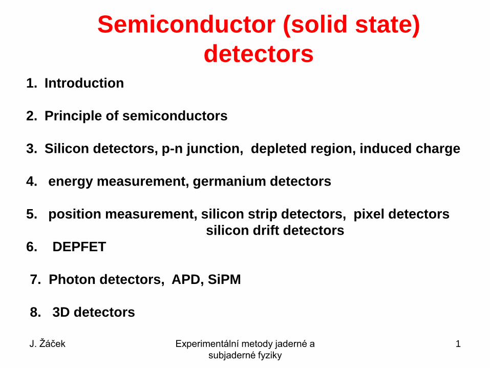
Semiconductor (solid state) detectors 1. Introduction 2. Principle of semiconductors 3. Silicon detectors, p-n junction, depleted region, induced charge 4. energy measurement, germanium detectors 5. position measurement, silicon strip detectors, pixel detectors silicon drift detectors 6. DEPFET 7. Photon detectors, APD, SiPM 8. 3D detectors J. Žáček Experimentální metody jaderné a subjaderné fyziky 1

Welcome message from author
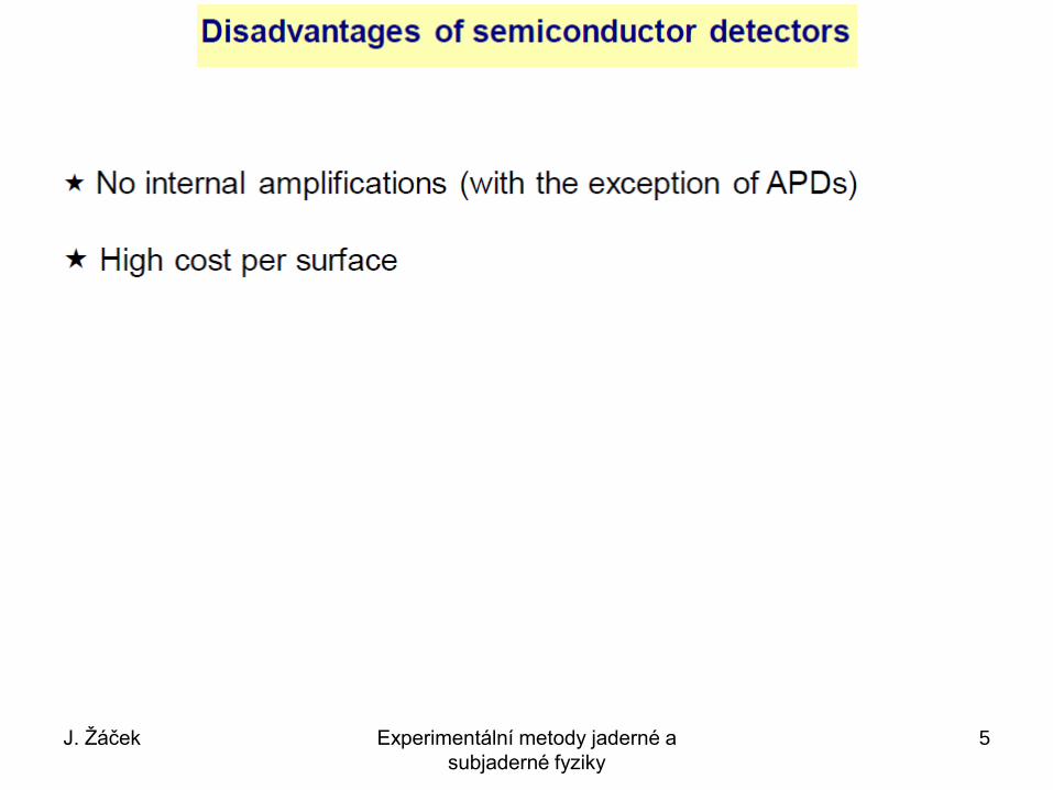
This document is posted to help you gain knowledge. Please leave a comment to let me know what you think about it! Share it to your friends and learn new things together.
Transcript
Semiconductor (solid state)
detectors 1. Introduction
2. Principle of semiconductors
3. Silicon detectors, p-n junction, depleted region, induced charge
4. energy measurement, germanium detectors
5. position measurement, silicon strip detectors, pixel detectors
silicon drift detectors
6. DEPFET
7. Photon detectors, APD, SiPM
8. 3D detectors
J. Žáček Experimentální metody jaderné a
subjaderné fyziky
1

1. Introduction
J. Žáček Experimentální metody jaderné a
subjaderné fyziky
2

J. Žáček Experimentální metody jaderné a
subjaderné fyziky
3

J. Žáček Experimentální metody jaderné a
subjaderné fyziky
4
J. Žáček Experimentální metody jaderné a
subjaderné fyziky
5
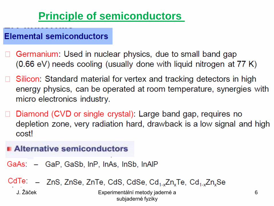
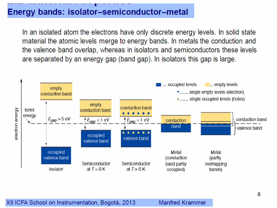
Principle of semiconductors
J. Žáček Experimentální metody jaderné a
subjaderné fyziky
6

hole conduction
J. Žáček Experimentální metody jaderné a
subjaderné fyziky
7
8
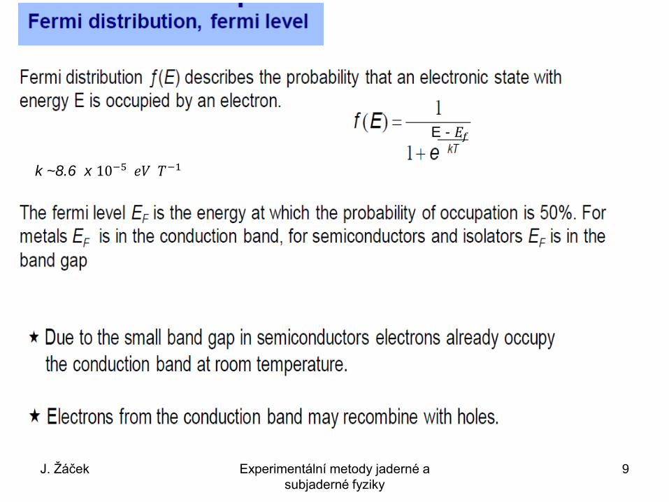
- E - 𝐸𝑓
J. Žáček Experimentální metody jaderné a
subjaderné fyziky
9
k ~8.6 x 10⁻⁵ 𝑒𝑉 𝑇−1

electron concentration
g(E) - density of electron state in the conduction band
f(E) ⦁ g( E) – electron concentration
𝑬𝒄 lowest energy level in the conduction band
g(𝑬𝒄 ) ≡ 𝑵𝒄 density of electron states in the lowest energy level
approximation : f ≈ 𝒆− ( 𝑬−𝑬𝒇)/𝒌𝑻
electron concentration in the lowest energy level 𝒏𝒆 = 𝑵𝒄 𝒆−
𝑬𝒄 −𝑬𝒇
𝒌𝑻
hole concentration
𝑬𝑽 − 𝐡𝐢𝐠𝐡𝐞𝐬𝐭 𝐞𝐧𝐞𝐫𝐠𝐲 𝐥𝐞𝐯𝐞𝐥 𝐢𝐧 𝐭𝐡𝐞 𝐯𝐚𝐥𝐞𝐧𝐜𝐞 𝐛𝐚𝐧𝐝
𝑵𝑽 - density of hole state in the highest energy level of the valence band
hole concentration in the highest energy level 𝒏𝒉 = 𝑵𝑽 𝒆−
𝑬𝒇 −𝑬𝒗
𝒌𝑻
J. Žáček Experimentální metody jaderné a
subjaderné fyziky
10
Boltzmann constant k ≈ 8.6 ⦁ 10−5 eV ⦁ 𝐾−1
E-𝐸𝑓 ≈ 1 𝑒𝑉
𝐸𝑔 = 𝐸𝑐 - 𝐸𝑉
J. Žáček Experimentální metody jaderné a
subjaderné fyziky
11
J. Žáček Experimentální metody jaderné a
subjaderné fyziky
12
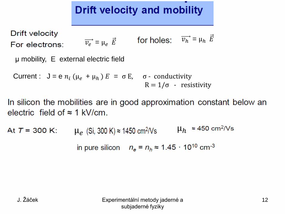
𝑣𝑒 = μ𝑒 𝐸 𝑣ℎ = μℎ 𝐸
μ mobility, E external electric field
Current : J = e 𝑛𝑖 (μ𝑒 + μℎ ) 𝐸 = σ E, σ - conductivity R = 1/σ - resistivity
μ𝑒 μℎ
13
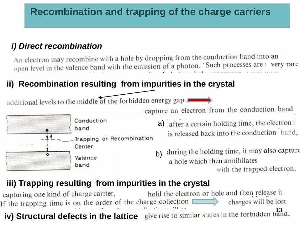
i) Direct recombination
Recombination and trapping of the charge carriers
ii) Recombination resulting from impurities in the crystal
a)
b)
iii) Trapping resulting from impurities in the crystal
iv) Structural defects in the lattice

J. Žáček Experimentální metody jaderné a
subjaderné fyziky
14
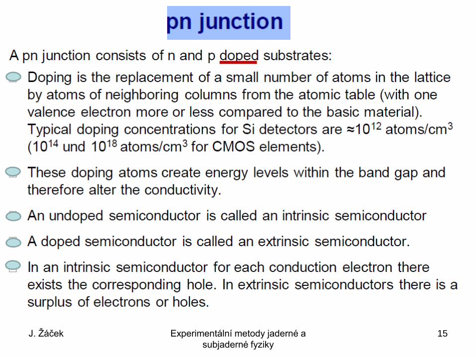
3. Silicon semiconductors, p – n junction
Si:
J. Žáček Experimentální metody jaderné a
subjaderné fyziky
15

J. Žáček Experimentální metody jaderné a
subjaderné fyziky
16
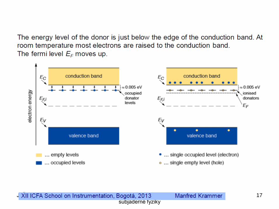
n- type semiconductor
J. Žáček Experimentální metody jaderné a
subjaderné fyziky
17

J. Žáček Experimentální metody jaderné a
subjaderné fyziky
18
p- type semiconductor

J. Žáček Experimentální metody jaderné a
subjaderné fyziky
19

J. Žáček Experimentální metody jaderné a
subjaderné fyziky
20

J. Žáček Experimentální metody jaderné a
subjaderné fyziky
21

J. Žáček Experimentální metody jaderné a
subjaderné fyziky
22

J. Žáček Experimentální metody jaderné a
subjaderné fyziky
23

24
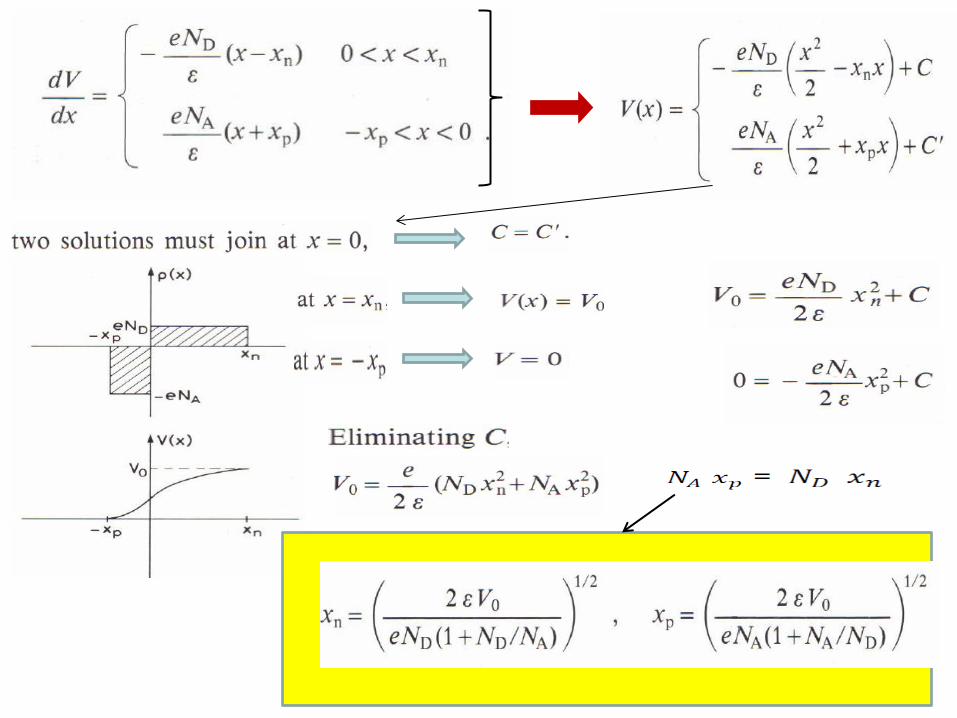
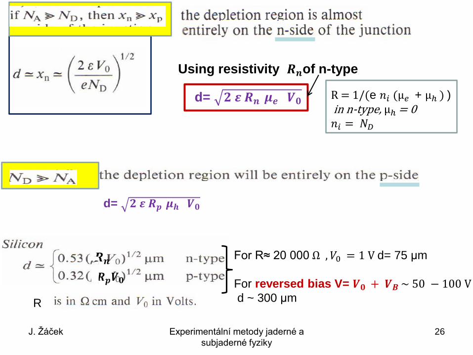
Approximation of charge densities
Concentration
of acceptors 𝑵𝑨 Concentration
of donors 𝑵𝑫
Maxwell equations:
25
J. Žáček Experimentální metody jaderné a
subjaderné fyziky
26
Using resistivity 𝑹𝒏of n-type
d= 𝟐 𝜺 𝑹𝒏 𝝁𝒆 𝑽𝟎
d= 𝟐 𝜺 𝑹𝒑 𝝁𝒉 𝑽𝟎
𝑹𝒏
𝑹𝒑𝑽𝟎
R
For R≈ 20 000 Ω , 𝑉0 = 1 V d= 75 μm
For reversed bias V= 𝑽𝟎 + 𝑽𝑩 ~ 50 − 100 V
d ~ 300 μm
R = 1/(e 𝑛𝑖 (μ𝑒 + μℎ ) ) in n-type, μℎ = 0 𝑛𝑖 = 𝑁𝐷

J. Žáček Experimentální metody jaderné a
subjaderné fyziky
27
𝑝+ over-dopped p-type
d
d
d
d

J. Žáček Experimentální metody jaderné a
subjaderné fyziky
28
J. Žáček Experimentální metody jaderné a
subjaderné fyziky
29
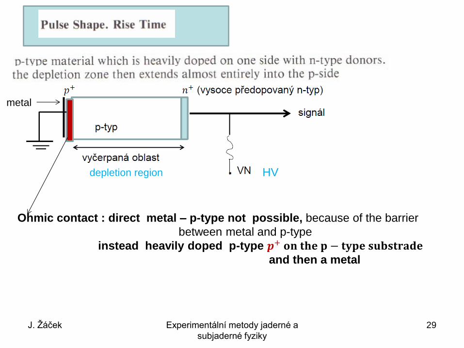
depletion region HV
Ohmic contact : direct metal – p-type not possible, because of the barrier
between metal and p-type
instead heavily doped p-type 𝒑+ 𝐨𝐧 𝐭𝐡𝐞 𝐩 − 𝐭𝐲𝐩𝐞 𝐬𝐮𝐛𝐬𝐭𝐫𝐚𝐝𝐞
and then a metal
metal

30
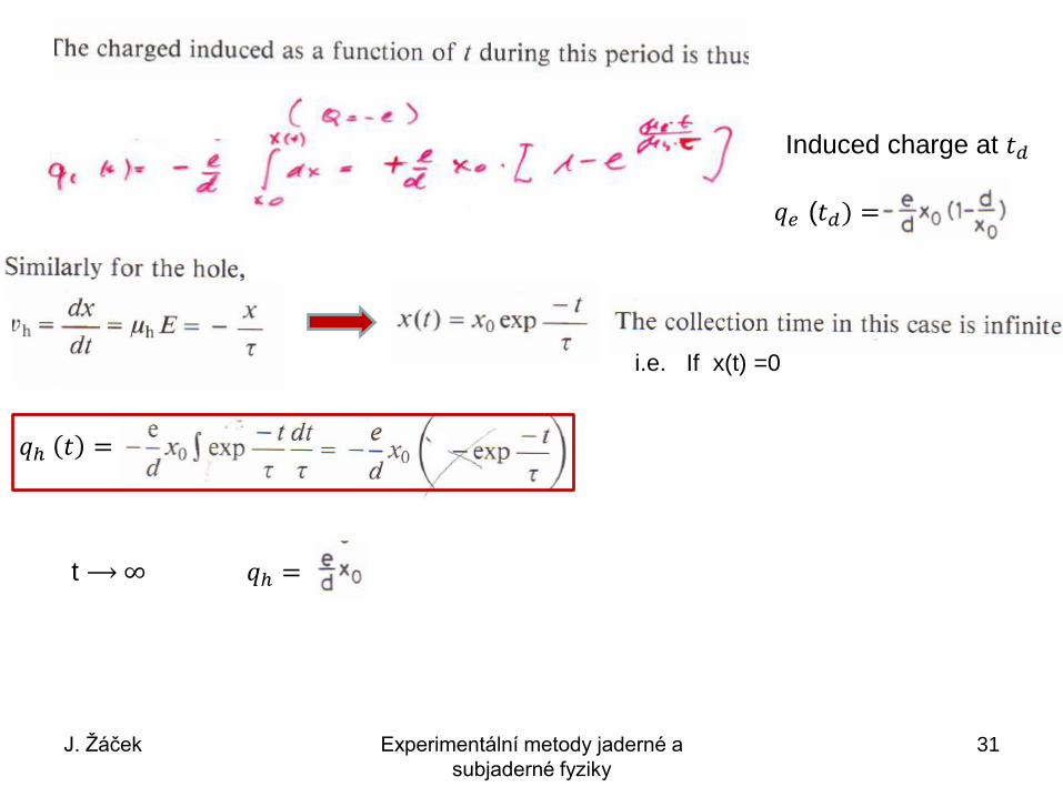
Induced charge
Q - charge in the depletion region
page 25:
but different coordinate frame,
zero at the junction
x ⟶ x - 𝑥𝑝 , 𝑥𝑝 ≡ d, E=-dV/dx
d - thickness of the depletion region
,resistivity R=1/( )
𝜏 = ε ⦁R
𝑡𝑑
J. Žáček Experimentální metody jaderné a
subjaderné fyziky
31
𝑞ℎ 𝑡 =
t ⟶ ∞ 𝑞ℎ =
𝑞𝑒 (𝑡𝑑) =
Induced charge at 𝑡𝑑
i.e. If x(t) =0

32
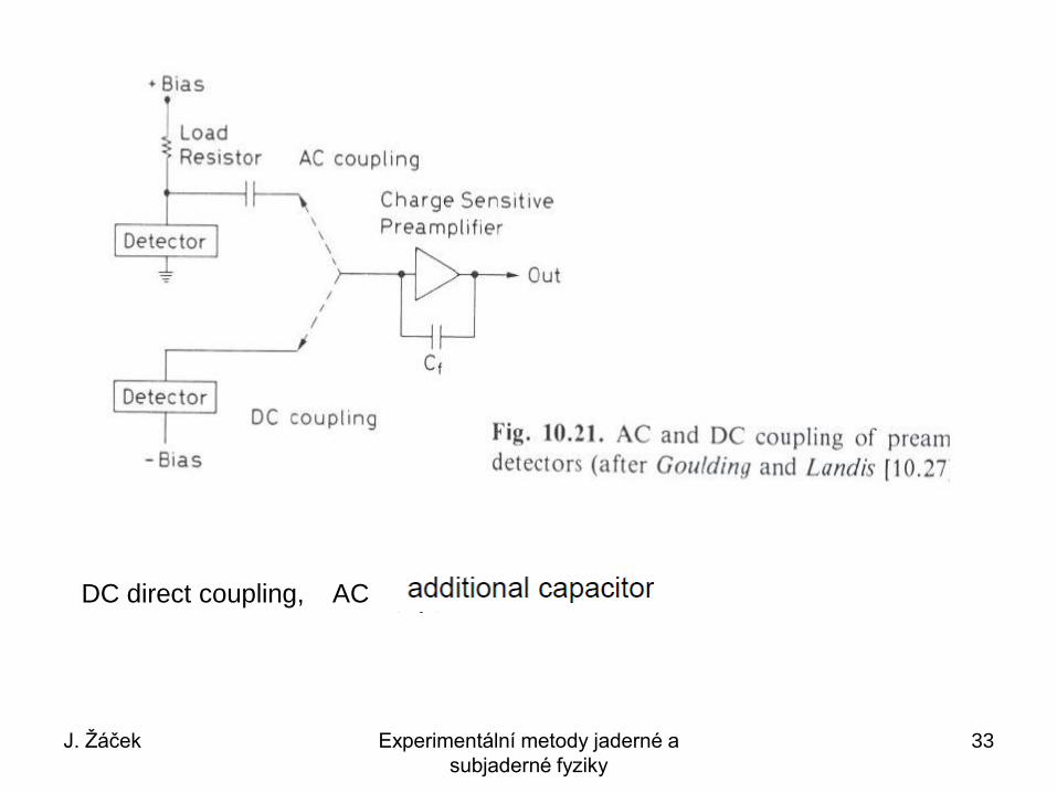
Ex. /pair
a good preamplifier needed, low noice
J. Žáček Experimentální metody jaderné a
subjaderné fyziky
33
DC direct coupling, AC

J. Žáček Experimentální metody jaderné a
subjaderné fyziky
34
4. Energy measurement
Construction of p-n junctions
• Diffused junction diode: diffusion of donors to p-type at the temperature
1000 C
• Surface barrier junction: junction between a semiconductor and a
metal
n-type Si with Au, p-type Si with Al
sensitive to light
• Ion-implanted junctions: a substrate is bombarded by ions from an
accelerator
Depleted region small ⟹ energy measurement for low energies

J. Žáček Experimentální metody jaderné a
subjaderné fyziky
35
Guard ring
J. Žáček Experimentální metody jaderné a
subjaderné fyziky
36
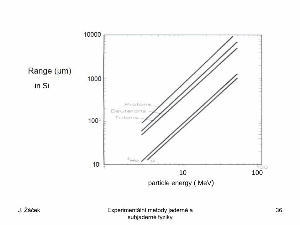
in Si
particle energy ( MeV)
10 100

J. Žáček Experimentální metody jaderné a
subjaderné fyziky
37
Compensating materials developed to increase the depletion region
by lithium drifting process
known as p-i-n junction
Li diffused to p-type, a narrow n-type is created
electrons drifted to p-type, negative space charge
application of HV ⟶ positive Li ions drifted to p-type
for sufficient time to create
⟹ the same concentration of positive ions and electrons t ⟹ no space charge, i.e. compensated region
resistivity up to 100 000 Ω width of compensating region 10-15 mm Si(Li) , the noise is much greater then in normal Si cooling is needed

J. Žáček Experimentální metody jaderné a
subjaderné fyziky
38
Energy resolution
Fluctuation of energy losses in the depleted region
Landau fluctuation
, Δ𝐸𝑚.𝑝. most probable energy loss

J. Žáček Experimentální metody jaderné a
subjaderné fyziky
39
Germanium detectors suitable for γ detection,
Resolution at 1.33 Mev Ge detector 0.15 %
NaI 8 %
-
- High purity germanium (PHGe), depletion region~ cm, low temperature during
- measurement only
J. Žáček Experimentální metody jaderné a
subjaderné fyziky
40
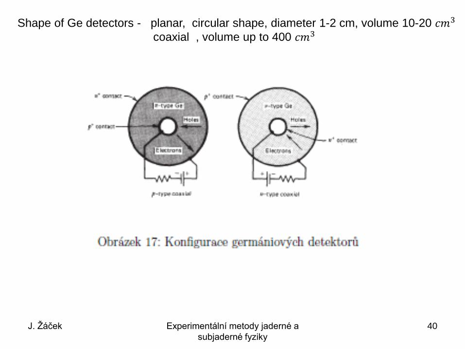
Shape of Ge detectors - planar, circular shape, diameter 1-2 cm, volume 10-20 𝑐𝑚3
coaxial , volume up to 400 𝑐𝑚3
J. Žáček Experimentální metody jaderné a
subjaderné fyziky
41
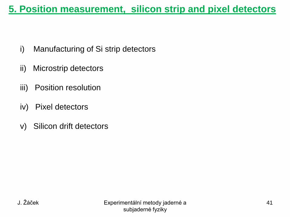
5. Position measurement, silicon strip and pixel detectors
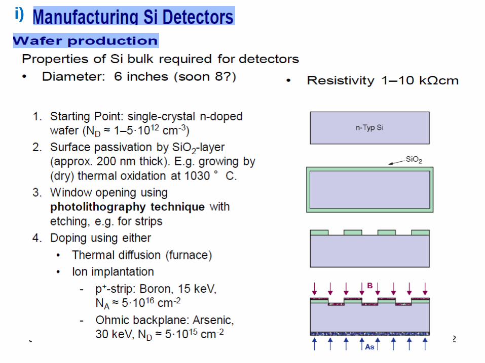
i) Manufacturing of Si strip detectors
ii) Microstrip detectors
iii) Position resolution
iv) Pixel detectors
v) Silicon drift detectors
J. Žáček Experimentální metody jaderné a
subjaderné fyziky
42
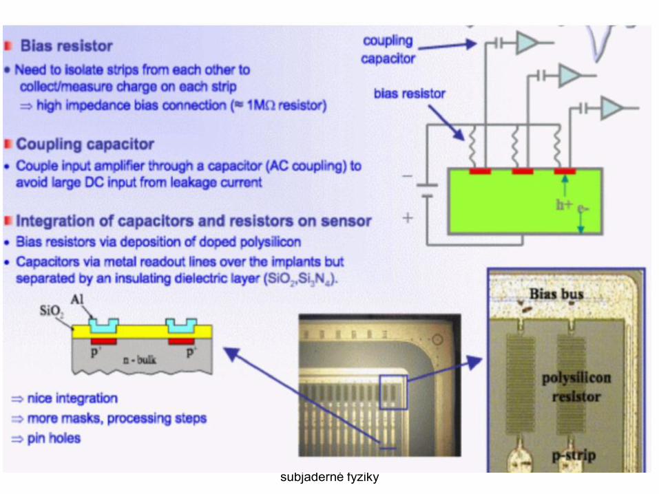
i)

J. Žáček Experimentální metody jaderné a
subjaderné fyziky
43

J. Žáček Experimentální metody jaderné a
subjaderné fyziky
44

J. Žáček Experimentální metody jaderné a
subjaderné fyziky
45
R
ii)
J. Žáček Experimentální metody jaderné a
subjaderné fyziky
46

J. Žáček Experimentální metody jaderné a
subjaderné fyziky
47

J. Žáček Experimentální metody jaderné a
subjaderné fyziky
48

J. Žáček Experimentální metody jaderné a
subjaderné fyziky
49
iii)

J. Žáček Experimentální metody jaderné a
subjaderné fyziky
50

J. Žáček Experimentální metody jaderné a
subjaderné fyziky
51

J. Žáček Experimentální metody jaderné a
subjaderné fyziky
52
analog readout

J. Žáček Experimentální metody jaderné a
subjaderné fyziky
53
iv)
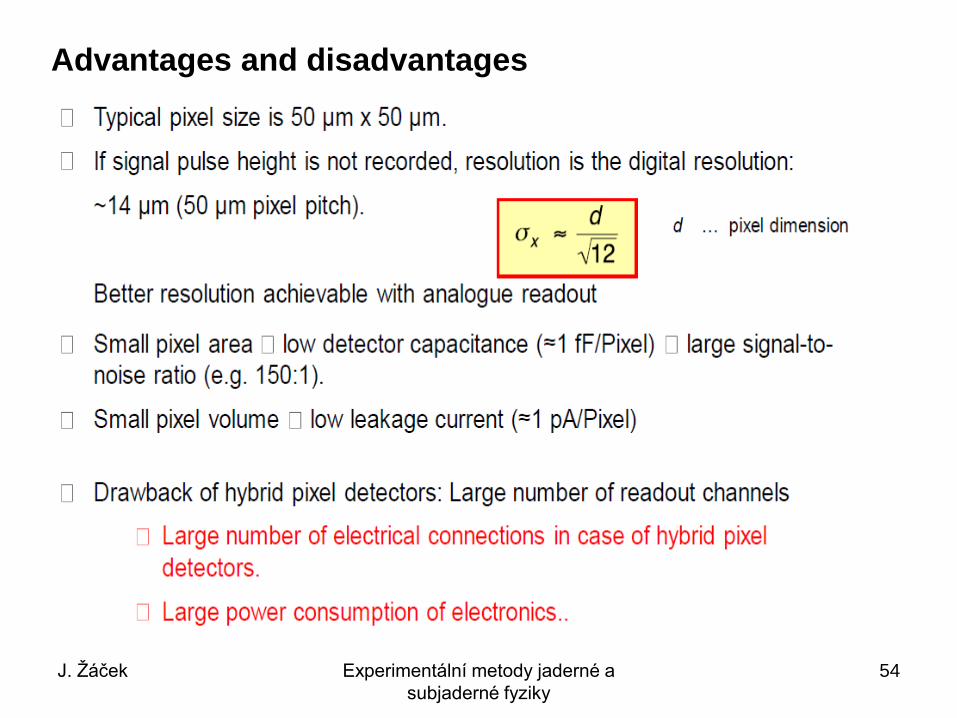
J. Žáček Experimentální metody jaderné a
subjaderné fyziky
54
Advantages and disadvantages

J. Žáček Experimentální metody jaderné a
subjaderné fyziky
55
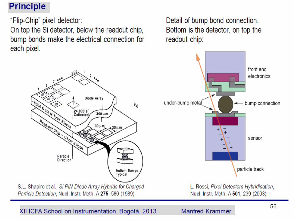
56
J. Žáček Experimentální metody jaderné a
subjaderné fyziky
57
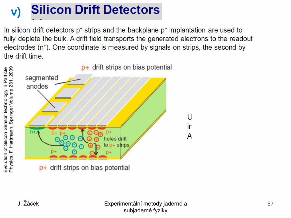
v)

J. Žáček Experimentální metody jaderné a
subjaderné fyziky
58
J. Žáček Experimentální metody jaderné a
subjaderné fyziky
59

J. Žáček Experimentální metody jaderné a
subjaderné fyziky
60
Application of strip, pixel and pad detectors
Trackers: precise determination of particle tracks (strips or pixels)
Vertex detectors: in collider experiments, detectors situated around
the interaction vertex
Topology: sensors mounted on a planar carbon frames or cylindrical carbon frames
Calorimeters: as active layers in sampling calorimeters

J. Žáček Experimentální metody jaderné a
subjaderné fyziky
61
forward and backward silicon tracker of the H1 experiment
Collider HERA, DESY Hamburg, electrons (~26 GeV) vs protons (920 GeV)
several layers of circular planes equipted with strip sensors
Interaction vertex
Beam pipe
electrons
protons
Emitted particle
electronics
Si sensors
sensor
particle

62
Pad silicon detectors for the readout of the
electromagnetic calorimeter CALICE
Si Si wafers 6 x 6 cm, 1 pad 1x1 cm, depletion
region 500 μm
calorimeter: absorber tungsten, active layers from Si wafers
electronic layer above active layer
(calorimeter for linear collider)
W - layer
Si wafers
readout board
63
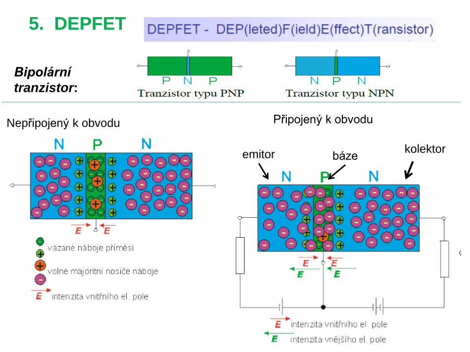
5. DEPFET
Bipolární
tranzistor:
Nepřipojený k obvodu Připojený k obvodu
emitor báze kolektor

J. Žáček Experimentální metody jaderné a
subjaderné fyziky
64
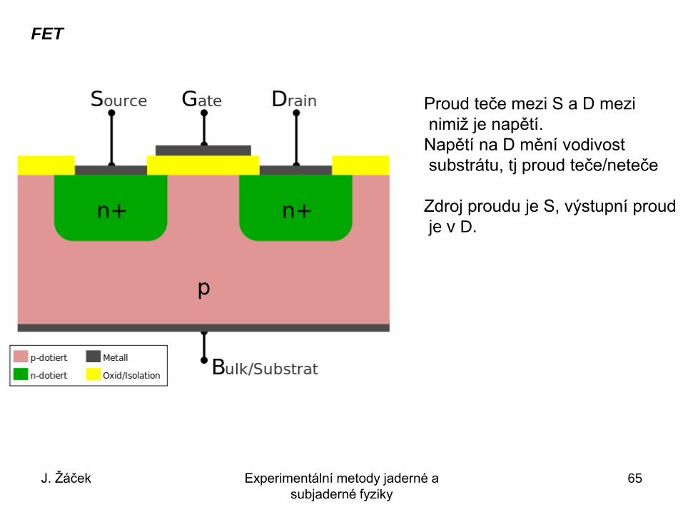
FET tranzistor
Polem řízené (neboli unipolární či FET) tranzistory spínají/omezují protékající proud
na základě toho, jaké napětí je na „drain“
řídicí se nazývá gate a značí se "G",
spínaný proud vstupuje do drainu "D" a
vystupuje z source "S". Tři jednotky FETu:
drain je zde jako kolektor, source jako emitor a gate jako báze
J. Žáček Experimentální metody jaderné a
subjaderné fyziky
65
FET
Proud teče mezi S a D mezi
nimiž je napětí.
Napětí na D mění vodivost
substrátu, tj proud teče/neteče
Zdroj proudu je S, výstupní proud
je v D.

J. Žáček Experimentální metody jaderné a
subjaderné fyziky
66
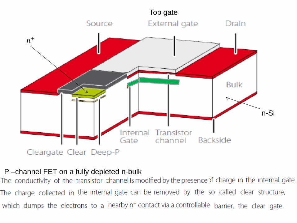
DEPFET je FET vytvořený na plně vyčerpanén substrátu. Působí současně jako
senzor a zesilovač
67
Top gate
P –channel FET on a fully depleted n-bulk
𝑛+
n-Si
J. Žáček Experimentální metody jaderné a
subjaderné fyziky
68
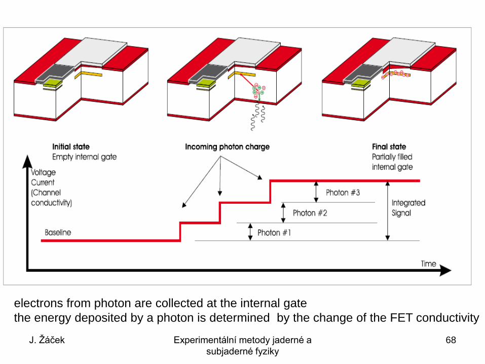
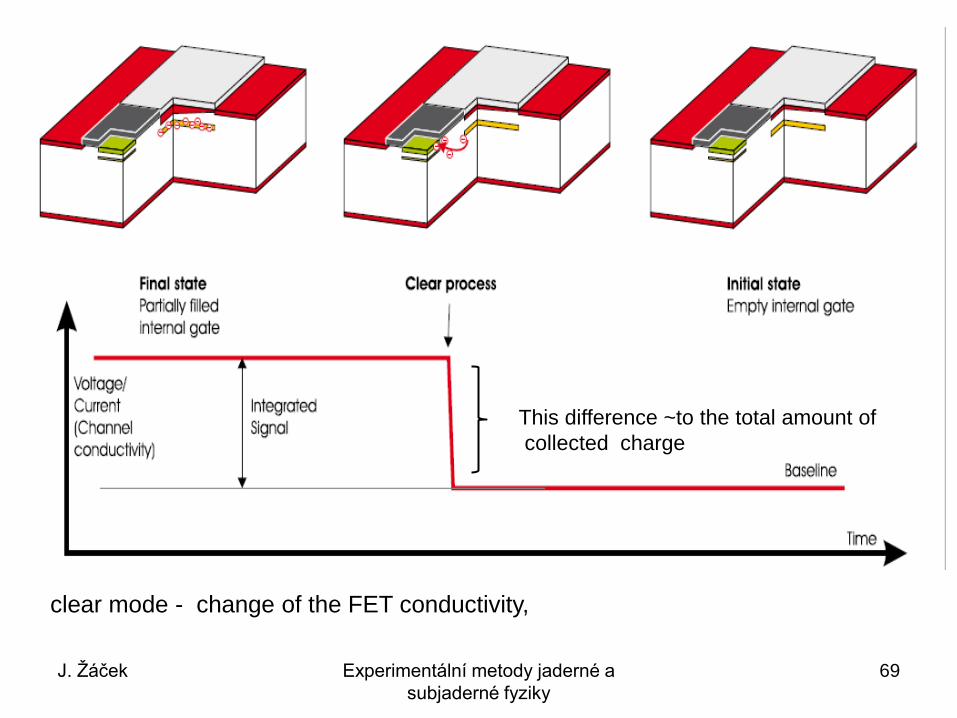
electrons from photon are collected at the internal gate
the energy deposited by a photon is determined by the change of the FET conductivity
J. Žáček Experimentální metody jaderné a
subjaderné fyziky
69
clear mode - change of the FET conductivity,
This difference ~to the total amount of
collected charge

J. Žáček Experimentální metody jaderné a
subjaderné fyziky
70
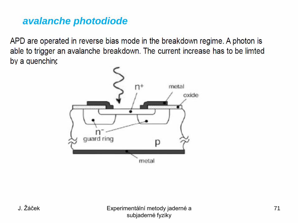
7. Semiconductor photon detectors
APD - avalanche photodiode replace e.g. photomultipliers in calorimeters, very small devices,
can be connected with fibers
Usual photodiode PD
J. Žáček Experimentální metody jaderné a
subjaderné fyziky
71
avalanche photodiode

J. Žáček Experimentální metody jaderné a
subjaderné fyziky
72

J. Žáček Experimentální metody jaderné a
subjaderné fyziky
73
HAPD - hybrid APD

J. Žáček Experimentální metody jaderné a
subjaderné fyziky
74
SiPM Silicon Photon Multipliers
1156 photodiodes on the area 1.1 x 1.1 𝑚𝑚2
depletion region

J. Žáček Experimentální metody jaderné a
subjaderné fyziky
75
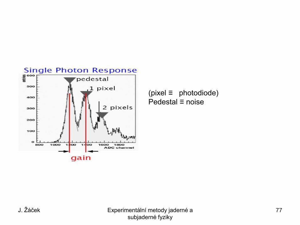
SiPM detects individual photons, current ~ to the number of fired pixels

76
Hadron calorimeter
Scintillation light from the tile is collected by a WLS fiber which is directly
connected to a SIPM.
WLS fibre
SiPM were first developed for the readout of scintillation light of the hadron
calorimeter within CALICE collaboration
J. Žáček Experimentální metody jaderné a
subjaderné fyziky
77
(pixel ≡ photodiode)
Pedestal ≡ noise
J. Žáček Experimentální metody jaderné a
subjaderné fyziky
78
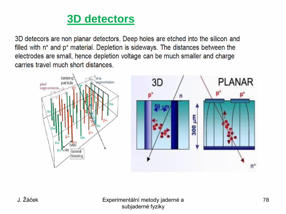
3D detectors
Related Documents


![[doi 10.1007%2F978-1-4020-2103-9_6] Shur, Michael S.; Žukauskas, Artūras -- UV Solid-State Light Emitters and Detectors __ UV Metal Semiconductor Metal Detectors (1).pdf](https://static.cupdf.com/doc/110x72/577c7d3a1a28abe0549de5a7/doi-1010072f978-1-4020-2103-96-shur-michael-s-zukauskas-arturas.jpg)


