Top Banner
1μm Semiconductor Processing: Thermal Oxides, Defects, impurities, and diffusion Professor Benjamín Alemán Department of Physics University of Oregon N C C Vacancy C
9

Semiconductor Processing: Thermal Oxides, Defects ... · Planar Processing with Semiconductors (Silicon): Course Map • Crystal growth ... Wet oxidation - (111) (100) 1.0 0.1 0.1

Jul 20, 2018

Download

Documents

trinhkiet
Welcome message from author
This document is posted to help you gain knowledge. Please leave a comment to let me know what you think about it! Share it to your friends and learn new things together.
Transcript
Page 1: Semiconductor Processing: Thermal Oxides, Defects ... · Planar Processing with Semiconductors (Silicon): Course Map • Crystal growth ... Wet oxidation - (111) (100) 1.0 0.1 0.1

1µm

Semiconductor Processing:

Thermal Oxides, Defects, impurities, and diffusion

Professor Benjamín AlemánDepartment of PhysicsUniversity of Oregon

N

CC

VacancyC

Page 2: Semiconductor Processing: Thermal Oxides, Defects ... · Planar Processing with Semiconductors (Silicon): Course Map • Crystal growth ... Wet oxidation - (111) (100) 1.0 0.1 0.1

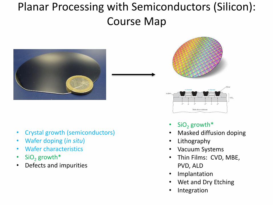
Planar Processing with Semiconductors (Silicon):Course Map

• Crystal growth (semiconductors)• Wafer doping (in situ)• Wafer characteristics• SiO2 growth*• Defects and impurities

• SiO2 growth*• Masked diffusion doping• Lithography• Vacuum Systems• Thin Films: CVD, MBE,

PVD, ALD• Implantation• Wet and Dry Etching• Integration
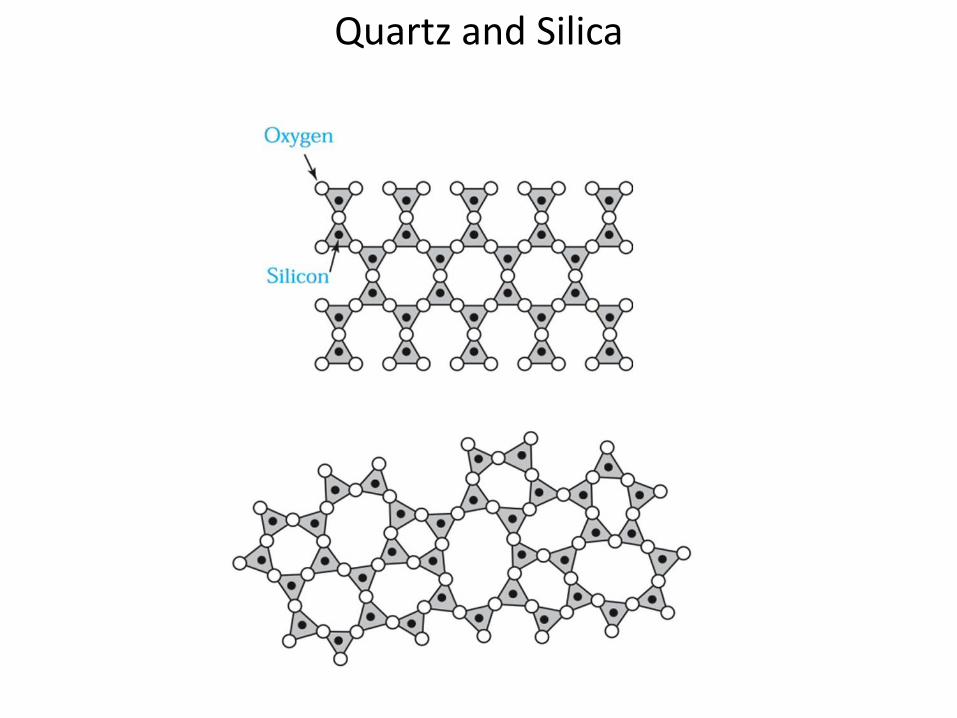
Page 3: Semiconductor Processing: Thermal Oxides, Defects ... · Planar Processing with Semiconductors (Silicon): Course Map • Crystal growth ... Wet oxidation - (111) (100) 1.0 0.1 0.1

Quartz and Silica

Page 4: Semiconductor Processing: Thermal Oxides, Defects ... · Planar Processing with Semiconductors (Silicon): Course Map • Crystal growth ... Wet oxidation - (111) (100) 1.0 0.1 0.1

Linear rate constant vs. Temperature

Factor of 10X

Page 5: Semiconductor Processing: Thermal Oxides, Defects ... · Planar Processing with Semiconductors (Silicon): Course Map • Crystal growth ... Wet oxidation - (111) (100) 1.0 0.1 0.1

Density of available bonds in (111) and (100) faces

6.78 × 10¹⁴ atoms/cm2 7.83 × 10¹⁴ atoms/cm2

Page 6: Semiconductor Processing: Thermal Oxides, Defects ... · Planar Processing with Semiconductors (Silicon): Course Map • Crystal growth ... Wet oxidation - (111) (100) 1.0 0.1 0.1

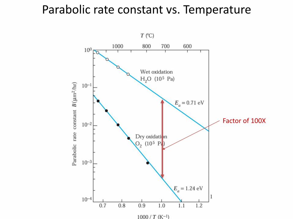
Parabolic rate constant vs. Temperature

Factor of 100X

Page 7: Semiconductor Processing: Thermal Oxides, Defects ... · Planar Processing with Semiconductors (Silicon): Course Map • Crystal growth ... Wet oxidation - (111) (100) 1.0 0.1 0.1

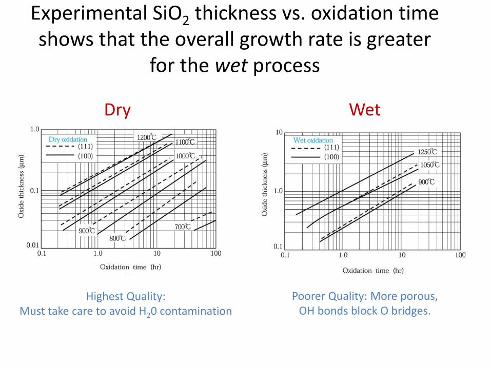
Experimental SiO2 thickness vs. oxidation time shows that the overall growth rate is greater

for the wet process

Dry Wet

Poorer Quality: More porous, OH bonds block O bridges.

Highest Quality:Must take care to avoid H20 contamination

Page 8: Semiconductor Processing: Thermal Oxides, Defects ... · Planar Processing with Semiconductors (Silicon): Course Map • Crystal growth ... Wet oxidation - (111) (100) 1.0 0.1 0.1

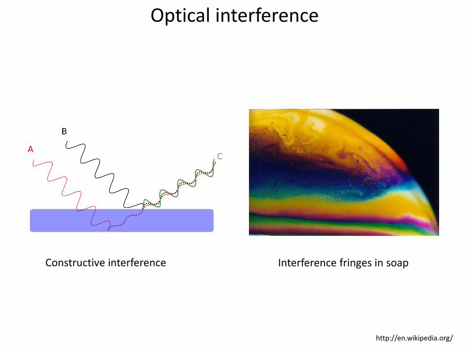
Optical interference

Constructive interference Interference fringes in soap

http://en.wikipedia.org/
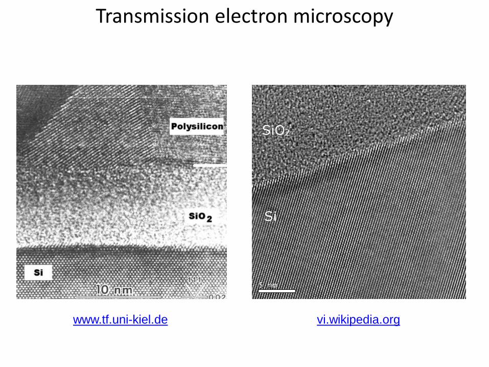