August 2012 SEMICONDUCTOR GENERAL CATALOG Transistors Bipolar Small-Signal Transistors Bipolar Power Transistors Junction FETs Combination Products of Different Type Devices MOSFETs Radio-Frequency Bipolar Small-Signal Transistors Radio-Frequency Small-Signal FETs Radio-Frequency Power MOSFETs IGBTs 1 2012/8 SCE0004M

Welcome message from author
This document is posted to help you gain knowledge. Please leave a comment to let me know what you think about it! Share it to your friends and learn new things together.
Transcript

August 2012
SEMICONDUCTOR GENERAL CATALOG
Transistors
Bipolar Small-Signal Transistors Bipolar Power Transistors
Junction FETs Combination Products of Different Type Devices
MOSFETs Radio-Frequency Bipolar Small-Signal Transistors
Radio-Frequency Small-Signal FETs Radio-Frequency Power MOSFETs
IGBTs
1 2012/8 SCE0004M

Bipolar Small-Signal Transistors
General-Purpose Transistor(Single)
ClassificationVCEO
(V)Max
IC(mA)Max
(Surface-Mount Type)
CST3 VESM SSM USM UFM
0.6
0.350.38
1.0
1.2
1.2
0.8
1.6
1.6
0.8
2.0
2.1
1.25
2.0
2.1
1.7
(mm) (mm) (mm) (mm) (mm)
NPN PNP NPN PNP NPN PNP NPN PNP NPN PNP
General-purpose
50100 2SC6026CT 2SA2154CT150 2SC6026MFV 2SA2154MFV 2SC4738 2SA1832 TTC4116* TTA1586*
30 500 2SC4118 2SA158850 500
Low noise 120 1002SC4117 2SA1587
Low saturation
voltage
12 400 2SC5376CT 2SC5376FV 2SA1955FV 2SC5376 2SA195512 500 2SC5233 2SA195415 800
High current
25 800
30 800
10 2000
20 2000
20 1500
20 2500 2SC6133 2SA221430 3000 2SA221550 1000 2SC613450 1700 2SC613550 2500 2SA2195
Strobe 10 5000(3000)
2SC6100
High breakdown
voltage80 300
High hFE 50 150
Muting 20 300 2SC4213High-speed switching 15 200
High-voltage switching 200 50
High breakdown
voltage
250 50
300 100
Darlington 40 300
x For the PNP transistors, the minus sign (–) indicating a negative voltage is omitted.
x Contact the Toshiba sales representative for information about RoHS compliance before you purchase any components.
2 2012/8 SCE0004M
Bipolar Small-Signal Transistors
General-Purpose Transistor(Single)
ClassificationVCEO
(V)Max
IC(mA)Max
(Surface-Mount Type)
CST3 VESM SSM USM UFM
0.6
0.350.38
1.0
1.2
1.2
0.8
1.6
1.6
0.8
2.0
2.1
1.25
2.0
2.1
1.7
(mm) (mm) (mm) (mm) (mm)
NPN PNP NPN PNP NPN PNP NPN PNP NPN PNP
General-purpose
50100 2SC6026CT 2SA2154CT150 2SC6026MFV 2SA2154MFV 2SC4738 2SA1832 TTC4116* TTA1586*
30 500 2SC4118 2SA158850 500
Low noise 120 1002SC4117 2SA1587
Low saturation
voltage
12 400 2SC5376CT 2SC5376FV 2SA1955FV 2SC5376 2SA195512 500 2SC5233 2SA195415 800
High current
25 800
30 800
10 2000
20 2000
20 1500
20 2500 2SC6133 2SA221430 3000 2SA221550 1000 2SC613450 1700 2SC613550 2500 2SA2195
Strobe 10 5000(3000)
2SC6100
High breakdown
voltage80 300
High hFE 50 150
Muting 20 300 2SC4213High-speed switching 15 200
High-voltage switching 200 50
High breakdown
voltage
250 50
300 100
Darlington 40 300
x For the PNP transistors, the minus sign (–) indicating a negative voltage is omitted.
x Contact the Toshiba sales representative for information about RoHS compliance before you purchase any components.
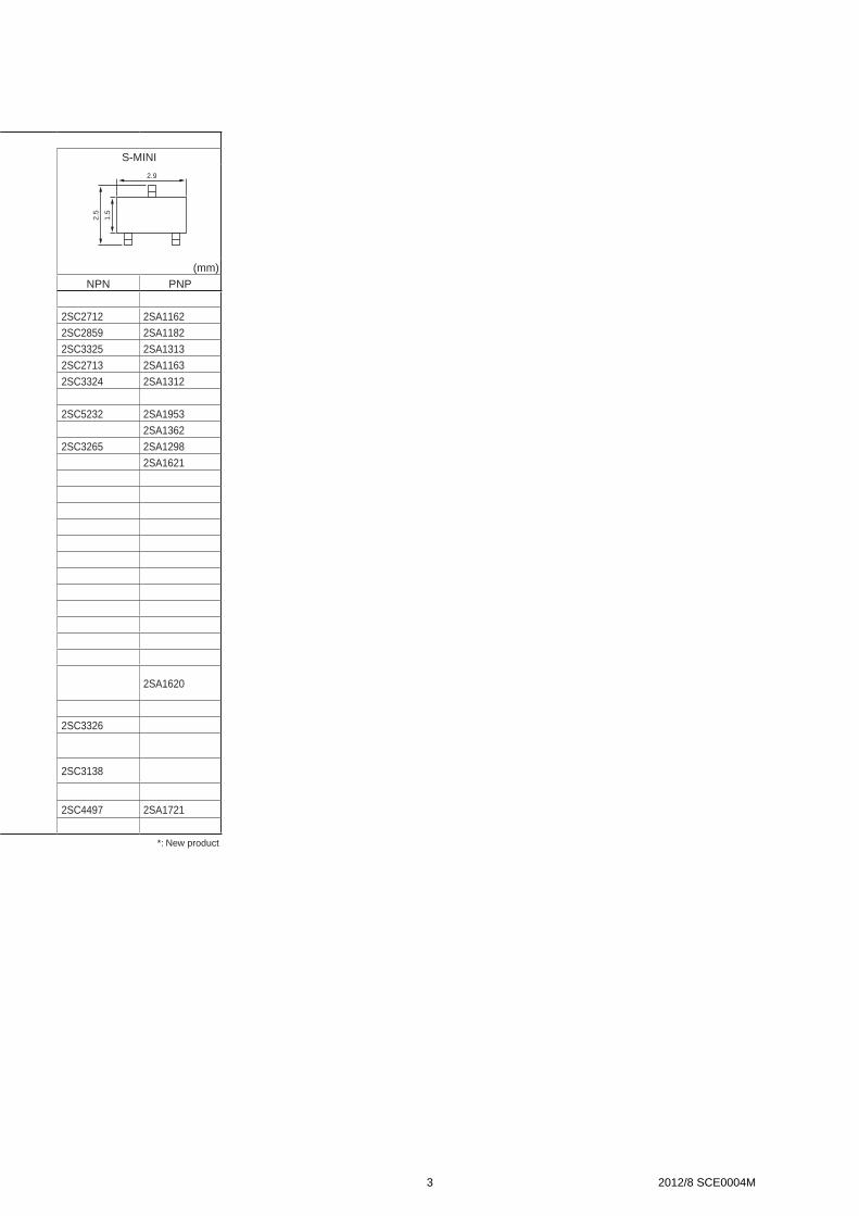
S-MINI
2.9
2.5
1.5
(mm)
NPN PNP
2SC2712 2SA1162
2SC2859 2SA1182
2SC3325 2SA1313
2SC2713 2SA1163
2SC3324 2SA1312
2SC5232 2SA1953
2SA1362
2SC3265 2SA1298
2SA1621
2SA1620
2SC3326
2SC3138
2SC4497 2SA1721
*: New product
3 2012/8 SCE0004M

(Dual)
ClassificationVCEO
(V)Max
IC(mA)Max
Dual Type
CST6 fS6 ESV USV SMV1.0
0.9
1.0
1.0
0.8
1.6
1.6
1.2
2.0
2.1
1.25
2.9
2.8
1.6
(mm) (mm) (mm) (mm) (mm)
NPN + PNP NPN PNP NPN + PNP PNP + NPN NPN PNP NPN PNP PNP + NPN
General-purpose
50 150(100)
(HN2B26CT) (HN1C26FS) (HN1A26FS) 2SA1873
(p18) (p10) (p7) (HN1B26FS) HN4B01JE 2SC4944 (p1) 2SC4207 2SA1618
(HN2C26FS) (HN2A26FS) (p9) (p6) (p2) HN4A56JU (p2) (p1)
(p12) (p11) (p4)
30 500HN4B04J
(p3) *
50 500
Low noise 120 100
HN4C06J HN4A06J
(p2) (p1) HN4B06J
HN4C51J HN4A51J (p3)
(p5) (p4)
High current
12 400HN4C05JU
(p2)12 500
15 800
30 800
10 2000
20 2000
Strobe 10 5000
High breakdown voltage 80 300
High hFE 50 150
Muting 20 300
High-speed switching 15 200
High-voltage switching 200 50
High breakdown voltage
250 50
300 100
Darlington 40 300
x For the PNP transistors, the minus sign (–) indicating a negative voltage is omitted.
x The ratings enclosed in parenthesis are for those devices whose part numbers are enclosed in parentheses.
x Contact the Toshiba sales representative for information about RoHS compliance before you purchase any components.
Internal ConnectionsNumber of Pins p1 p2 p3 p4 p5 p6
5 Q1 Q2 Q1 Q2 Q1 Q2 Q1 Q2 Q1 Q2 Q1 Q2
6
p7 p8 p9 p10 p11 p12
Q1 Q2 Q1 Q2 Q1 Q2 Q1 Q2 Q1 Q2 Q1 Q2
6
p13 p14 p15 p16 p17 p18
Q1
Q2
Q2
Q1 Q2
Q1
Q2
Q1
Q2
Q1 Q1 Q2
The internal connection diagrams only show the general configurations of the circuits.
4 2012/8 SCE0004M

(Dual)
ClassificationVCEO
(V)Max
IC(mA)Max
Dual Type
CST6 fS6 ESV USV SMV1.0
0.9
1.0
1.0
0.8
1.6
1.6
1.2
2.0
2.1
1.25
2.9
2.8
1.6
(mm) (mm) (mm) (mm) (mm)
NPN + PNP NPN PNP NPN + PNP PNP + NPN NPN PNP NPN PNP PNP + NPN
General-purpose
50 150(100)
(HN2B26CT) (HN1C26FS) (HN1A26FS) 2SA1873
(p18) (p10) (p7) (HN1B26FS) HN4B01JE 2SC4944 (p1) 2SC4207 2SA1618
(HN2C26FS) (HN2A26FS) (p9) (p6) (p2) HN4A56JU (p2) (p1)
(p12) (p11) (p4)
30 500HN4B04J
(p3) *
50 500
Low noise 120 100
HN4C06J HN4A06J
(p2) (p1) HN4B06J
HN4C51J HN4A51J (p3)
(p5) (p4)
High current
12 400HN4C05JU
(p2)12 500
15 800
30 800
10 2000
20 2000
Strobe 10 5000
High breakdown voltage 80 300
High hFE 50 150
Muting 20 300
High-speed switching 15 200
High-voltage switching 200 50
High breakdown voltage
250 50
300 100
Darlington 40 300
x For the PNP transistors, the minus sign (–) indicating a negative voltage is omitted.
x The ratings enclosed in parenthesis are for those devices whose part numbers are enclosed in parentheses.
x Contact the Toshiba sales representative for information about RoHS compliance before you purchase any components.
Internal ConnectionsNumber of Pins p1 p2 p3 p4 p5 p6
5 Q1 Q2 Q1 Q2 Q1 Q2 Q1 Q2 Q1 Q2 Q1 Q2
6
p7 p8 p9 p10 p11 p12
Q1 Q2 Q1 Q2 Q1 Q2 Q1 Q2 Q1 Q2 Q1 Q2
6
p13 p14 p15 p16 p17 p18
Q1
Q2
Q2
Q1 Q2
Q1
Q2
Q1
Q2
Q1 Q1 Q2
ES6 US6 SM61.6
1.6
1.2
2.0
2.1
1.25
2.9
2.8
1.6
(mm) (mm) (mm)
NPN PNP PNP + NPN NPN PNP PNP + NPN NPN PNP PNP + NPN
HN1C01FE HN1C01FU HN1B01FU
(p10) HN1A01FE (p10) HN1A01FU (p8) HN1A01F HN1B01F
HN2C01FE (p7) HN1B04FE HN2C01FU (p7) HN1B04FU HN1C01F (p7) (p8)
(p12) HN2A01FE (p9) (p12) HN2A01FU (p9) (p10) HN3A56F HN3B01F
HN3C67FE (p11) HN3C56FU (p11) HN3B02FU (p16) (p13)
(p17) (p15) (p14)
HN1B04F
(p8)
HN1C07F HN1A07F
(p10) (p7)
HN3C51F HN3A51F
(p15) (p16)
HN1C05FE
(p10)
HN1A02F
(p7)
HN1C03FU HN1C03F
(p10) (p10)
*: New product
5 2012/8 SCE0004M
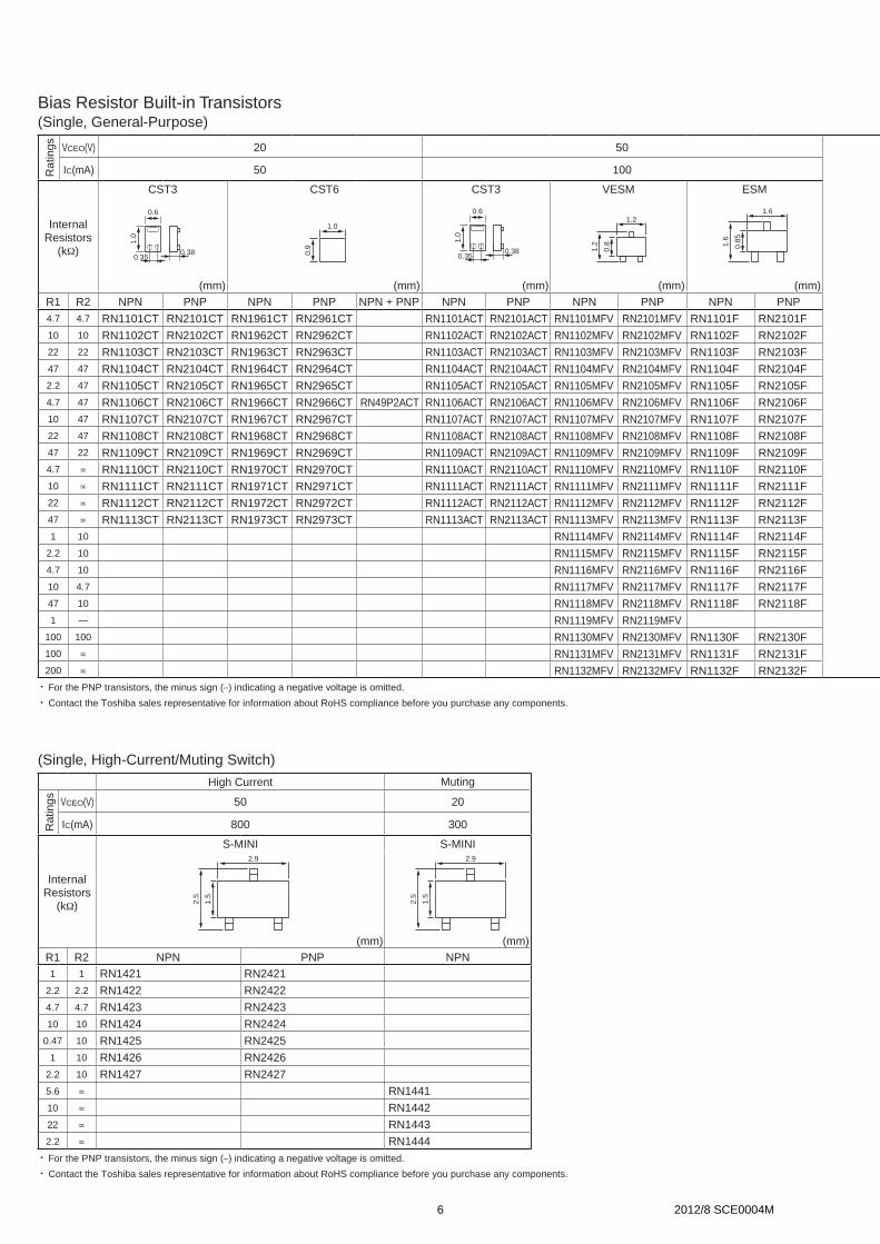
Bias Resistor Built-in Transistors(Single, General-Purpose)
Rat
ings VCEO(V) 20 50
IC(mA) 50 100
Internal Resistors
(kΩ)
CST3 CST6 CST3 VESM ESM
0.6
0.350.38
1.0
(mm)
1.0
0.9
(mm)
0.6
0.350.38
1.0
(mm)
1.2
1.2
0.8
(mm)
1.6
1.6
0.85
(mm)R1 R2 NPN PNP NPN PNP NPN + PNP NPN PNP NPN PNP NPN PNP4.7 4.7 RN1101CT RN2101CT RN1961CT RN2961CT RN1101ACT RN2101ACT RN1101MFV RN2101MFV RN1101F RN2101F10 10 RN1102CT RN2102CT RN1962CT RN2962CT RN1102ACT RN2102ACT RN1102MFV RN2102MFV RN1102F RN2102F22 22 RN1103CT RN2103CT RN1963CT RN2963CT RN1103ACT RN2103ACT RN1103MFV RN2103MFV RN1103F RN2103F47 47 RN1104CT RN2104CT RN1964CT RN2964CT RN1104ACT RN2104ACT RN1104MFV RN2104MFV RN1104F RN2104F2.2 47 RN1105CT RN2105CT RN1965CT RN2965CT RN1105ACT RN2105ACT RN1105MFV RN2105MFV RN1105F RN2105F4.7 47 RN1106CT RN2106CT RN1966CT RN2966CT RN49P2ACT RN1106ACT RN2106ACT RN1106MFV RN2106MFV RN1106F RN2106F10 47 RN1107CT RN2107CT RN1967CT RN2967CT RN1107ACT RN2107ACT RN1107MFV RN2107MFV RN1107F RN2107F22 47 RN1108CT RN2108CT RN1968CT RN2968CT RN1108ACT RN2108ACT RN1108MFV RN2108MFV RN1108F RN2108F47 22 RN1109CT RN2109CT RN1969CT RN2969CT RN1109ACT RN2109ACT RN1109MFV RN2109MFV RN1109F RN2109F4.7 ∞ RN1110CT RN2110CT RN1970CT RN2970CT RN1110ACT RN2110ACT RN1110MFV RN2110MFV RN1110F RN2110F10 ∞ RN1111CT RN2111CT RN1971CT RN2971CT RN1111ACT RN2111ACT RN1111MFV RN2111MFV RN1111F RN2111F22 ∞ RN1112CT RN2112CT RN1972CT RN2972CT RN1112ACT RN2112ACT RN1112MFV RN2112MFV RN1112F RN2112F47 ∞ RN1113CT RN2113CT RN1973CT RN2973CT RN1113ACT RN2113ACT RN1113MFV RN2113MFV RN1113F RN2113F1 10 RN1114MFV RN2114MFV RN1114F RN2114F
2.2 10 RN1115MFV RN2115MFV RN1115F RN2115F4.7 10 RN1116MFV RN2116MFV RN1116F RN2116F10 4.7 RN1117MFV RN2117MFV RN1117F RN2117F47 10 RN1118MFV RN2118MFV RN1118F RN2118F1 — RN1119MFV RN2119MFV
100 100 RN1130MFV RN2130MFV RN1130F RN2130F100 ∞ RN1131MFV RN2131MFV RN1131F RN2131F200 ∞ RN1132MFV RN2132MFV RN1132F RN2132F x For the PNP transistors, the minus sign (–) indicating a negative voltage is omitted.
x Contact the Toshiba sales representative for information about RoHS compliance before you purchase any components.
(Single, High-Current/Muting Switch)
High Current Muting
Rat
ings VCEO(V) 50 20
IC(mA) 800 300
Internal Resistors
(kΩ)
S-MINI S-MINI2.9
2.5
1.5
(mm)
2.9
2.5
1.5
(mm)R1 R2 NPN PNP NPN1 1 RN1421 RN2421
2.2 2.2 RN1422 RN24224.7 4.7 RN1423 RN242310 10 RN1424 RN2424
0.47 10 RN1425 RN24251 10 RN1426 RN2426
2.2 10 RN1427 RN24275.6 ∞ RN144110 ∞ RN144222 ∞ RN14432.2 ∞ RN1444 x For the PNP transistors, the minus sign (–) indicating a negative voltage is omitted.
x Contact the Toshiba sales representative for information about RoHS compliance before you purchase any components.
6 2012/8 SCE0004M

Bias Resistor Built-in Transistors(Single, General-Purpose)
Rat
ings VCEO(V) 20 50
IC(mA) 50 100
Internal Resistors
(kΩ)
CST3 CST6 CST3 VESM ESM
0.6
0.350.38
1.0
(mm)
1.0
0.9
(mm)
0.6
0.350.38
1.0
(mm)
1.2
1.2
0.8
(mm)
1.6
1.6
0.85
(mm)R1 R2 NPN PNP NPN PNP NPN + PNP NPN PNP NPN PNP NPN PNP4.7 4.7 RN1101CT RN2101CT RN1961CT RN2961CT RN1101ACT RN2101ACT RN1101MFV RN2101MFV RN1101F RN2101F10 10 RN1102CT RN2102CT RN1962CT RN2962CT RN1102ACT RN2102ACT RN1102MFV RN2102MFV RN1102F RN2102F22 22 RN1103CT RN2103CT RN1963CT RN2963CT RN1103ACT RN2103ACT RN1103MFV RN2103MFV RN1103F RN2103F47 47 RN1104CT RN2104CT RN1964CT RN2964CT RN1104ACT RN2104ACT RN1104MFV RN2104MFV RN1104F RN2104F2.2 47 RN1105CT RN2105CT RN1965CT RN2965CT RN1105ACT RN2105ACT RN1105MFV RN2105MFV RN1105F RN2105F4.7 47 RN1106CT RN2106CT RN1966CT RN2966CT RN49P2ACT RN1106ACT RN2106ACT RN1106MFV RN2106MFV RN1106F RN2106F10 47 RN1107CT RN2107CT RN1967CT RN2967CT RN1107ACT RN2107ACT RN1107MFV RN2107MFV RN1107F RN2107F22 47 RN1108CT RN2108CT RN1968CT RN2968CT RN1108ACT RN2108ACT RN1108MFV RN2108MFV RN1108F RN2108F47 22 RN1109CT RN2109CT RN1969CT RN2969CT RN1109ACT RN2109ACT RN1109MFV RN2109MFV RN1109F RN2109F4.7 ∞ RN1110CT RN2110CT RN1970CT RN2970CT RN1110ACT RN2110ACT RN1110MFV RN2110MFV RN1110F RN2110F10 ∞ RN1111CT RN2111CT RN1971CT RN2971CT RN1111ACT RN2111ACT RN1111MFV RN2111MFV RN1111F RN2111F22 ∞ RN1112CT RN2112CT RN1972CT RN2972CT RN1112ACT RN2112ACT RN1112MFV RN2112MFV RN1112F RN2112F47 ∞ RN1113CT RN2113CT RN1973CT RN2973CT RN1113ACT RN2113ACT RN1113MFV RN2113MFV RN1113F RN2113F1 10 RN1114MFV RN2114MFV RN1114F RN2114F
2.2 10 RN1115MFV RN2115MFV RN1115F RN2115F4.7 10 RN1116MFV RN2116MFV RN1116F RN2116F10 4.7 RN1117MFV RN2117MFV RN1117F RN2117F47 10 RN1118MFV RN2118MFV RN1118F RN2118F1 — RN1119MFV RN2119MFV
100 100 RN1130MFV RN2130MFV RN1130F RN2130F100 ∞ RN1131MFV RN2131MFV RN1131F RN2131F200 ∞ RN1132MFV RN2132MFV RN1132F RN2132F x For the PNP transistors, the minus sign (–) indicating a negative voltage is omitted.
x Contact the Toshiba sales representative for information about RoHS compliance before you purchase any components.
(Single, High-Current/Muting Switch)
High Current Muting
Rat
ings VCEO(V) 50 20
IC(mA) 800 300
Internal Resistors
(kΩ)
S-MINI S-MINI2.9
2.5
1.5
(mm)
2.9
2.5
1.5
(mm)R1 R2 NPN PNP NPN1 1 RN1421 RN2421
2.2 2.2 RN1422 RN24224.7 4.7 RN1423 RN242310 10 RN1424 RN2424
0.47 10 RN1425 RN24251 10 RN1426 RN2426
2.2 10 RN1427 RN24275.6 ∞ RN144110 ∞ RN144222 ∞ RN14432.2 ∞ RN1444 x For the PNP transistors, the minus sign (–) indicating a negative voltage is omitted.
x Contact the Toshiba sales representative for information about RoHS compliance before you purchase any components.
50
100
SSM USM S-MINI
1.6
1.6
0.8
(mm)
2.0
2.1
1.25
(mm)
2.9
2.5
1.5
(mm)NPN PNP NPN PNP NPN PNP
RN1101 RN2101 RN1301 RN2301 RN1401 RN2401
RN1102 RN2102 RN1302 RN2302 RN1402 RN2402
RN1103 RN2103 RN1303 RN2303 RN1403 RN2403
RN1104 RN2104 RN1304 RN2304 RN1404 RN2404
RN1105 RN2105 RN1305 RN2305 RN1405 RN2405
RN1106 RN2106 RN1306 RN2306 RN1406 RN2406
RN1107 RN2107 RN1307 RN2307 RN1407 RN2407
RN1108 RN2108 RN1308 RN2308 RN1408 RN2408
RN1109 RN2109 RN1309 RN2309 RN1409 RN2409
RN1110 RN2110 RN1310 RN2310 RN1410 RN2410
RN1111 RN2111 RN1311 RN2311 RN1411 RN2411
RN1112 RN2112 RN1312 RN2312 RN1412 RN2412
RN1113 RN2113 RN1313 RN2313 RN1413 RN2413
RN1114 RN2114 RN1314 RN2314 RN1414 RN2414
RN1115 RN2115 RN1315 RN2315 RN1415 RN2415
RN1116 RN2116 RN1316 RN2316 RN1416 RN2416
RN1117 RN2117 RN1317 RN2317 RN1417 RN2417
RN1118 RN2118 RN1318 RN2318 RN1418 RN2418
7 2012/8 SCE0004M

Bias Resistor Built-in Transistors(Dual, General-Purpose)
Classification
Absolute Maximum Ratings
Internal Resistors ESV USV
VCEO IC Q1 Q21.6
1.6
1.2
(mm)
2.0
2.1
1.25
(mm)NPN x 2 PNP x 2 NPN + PNP NPN x 2 PNP x 2 NPN + PNP
Q1
R1 R1
R2 R2
Q2 Q1
R1 R1
R2 R2
Q2
R1
R1
Q1
Q2
R2
R2
Q1
R1 R1
R2 R2
Q2 Q1
R1 R1
R2 R2
Q2
R1
R1
Q1
Q2
R2
R2
(kΩ) (kΩ)R1 R2 R1 R2
(V) (mA) Common emitter Common emitterCollector-base
connectionCommon emitter Common emitter
Collector-base connection
General-purpose
50 100
4.7 4.7 4.7 4.7 RN1701JE RN2701JE RN1701 RN270110 10 10 10 RN1702JE RN2702JE RN47A3JE RN1702 RN2702 RN47A322 22 22 22 RN1703JE RN2703JE RN47A2JE RN1703 RN2703 RN47A247 47 47 47 RN1704JE RN2704JE RN1704 RN27042.2 47 2.2 47 RN1705JE RN2705JE RN1705 RN27054.7 47 4.7 47 RN1706JE RN2706JE RN1706 RN270610 47 10 47 RN1707JE RN2707JE RN1707 RN270722 47 22 47 RN1708JE RN2708JE RN1708 RN270847 22 47 22 RN1709JE RN2709JE RN1709 RN27094.7 — 4.7 — RN1710JE RN2710JE RN47A1JE RN1710 RN2710 RN47A110 — 10 — RN1711JE RN2711JE RN1711 RN271122 — 22 — RN2712JE47 — 47 — RN2713JE1 10 1 10 RN2714
2.2 10 2.2 10
4.7 10 4.7 10
10 4.7 10 4.7
47 10 47 10
47 47 10 47 RN47A4JE RN47A447 47 4.7 10 RN47A5JE RN47A5100 100 100 100 RN47A610 10 47 10 RN47A7
Q1: 50 Q1: 100
10 10 4.7 10 RN47A7JEQ2: 12 Q2: 100
(Lowsat)
Q1: 50 Q1: 100
10 10 10 47 RN47A8JEQ2: 30 Q2: 100
(High hFE)
Muting 20 300 2.2 — 2.2 —
x For the PNP transistors, the minus sign (–) indicating a negative voltage is omitted.
x Contact the Toshiba sales representative for information about RoHS compliance before you purchase any components.
8 2012/8 SCE0004M

Bias Resistor Built-in Transistors(Dual, General-Purpose)
Classification
Absolute Maximum Ratings
Internal Resistors ESV USV
VCEO IC Q1 Q21.6
1.6
1.2
(mm)
2.0
2.1
1.25
(mm)NPN x 2 PNP x 2 NPN + PNP NPN x 2 PNP x 2 NPN + PNP
Q1
R1 R1
R2 R2
Q2 Q1
R1 R1
R2 R2
Q2
R1
R1
Q1
Q2
R2
R2
Q1
R1 R1
R2 R2
Q2 Q1
R1 R1
R2 R2
Q2
R1
R1
Q1
Q2
R2
R2
(kΩ) (kΩ)R1 R2 R1 R2
(V) (mA) Common emitter Common emitterCollector-base
connectionCommon emitter Common emitter
Collector-base connection
General-purpose
50 100
4.7 4.7 4.7 4.7 RN1701JE RN2701JE RN1701 RN270110 10 10 10 RN1702JE RN2702JE RN47A3JE RN1702 RN2702 RN47A322 22 22 22 RN1703JE RN2703JE RN47A2JE RN1703 RN2703 RN47A247 47 47 47 RN1704JE RN2704JE RN1704 RN27042.2 47 2.2 47 RN1705JE RN2705JE RN1705 RN27054.7 47 4.7 47 RN1706JE RN2706JE RN1706 RN270610 47 10 47 RN1707JE RN2707JE RN1707 RN270722 47 22 47 RN1708JE RN2708JE RN1708 RN270847 22 47 22 RN1709JE RN2709JE RN1709 RN27094.7 — 4.7 — RN1710JE RN2710JE RN47A1JE RN1710 RN2710 RN47A110 — 10 — RN1711JE RN2711JE RN1711 RN271122 — 22 — RN2712JE47 — 47 — RN2713JE1 10 1 10 RN2714
2.2 10 2.2 10
4.7 10 4.7 10
10 4.7 10 4.7
47 10 47 10
47 47 10 47 RN47A4JE RN47A447 47 4.7 10 RN47A5JE RN47A5100 100 100 100 RN47A610 10 47 10 RN47A7
Q1: 50 Q1: 100
10 10 4.7 10 RN47A7JEQ2: 12 Q2: 100
(Lowsat)
Q1: 50 Q1: 100
10 10 10 47 RN47A8JEQ2: 30 Q2: 100
(High hFE)
Muting 20 300 2.2 — 2.2 —
x For the PNP transistors, the minus sign (–) indicating a negative voltage is omitted.
x Contact the Toshiba sales representative for information about RoHS compliance before you purchase any components.
SMV
2.9
2.8
1.6
(mm)NPN x 2 PNP x 2 NPN + PNP
Q1
R1 R1
R2 R2
Q2 Q1
R1 R1
R2 R2
Q2
R1
R1
Q1
Q2
R2
R2
Common emitter Common emitterCollector-base
connection
RN1501 RN2501
RN1502 RN2502
RN1503 RN2503
RN1504 RN2504
RN1505 RN2505
RN1506 RN2506
RN1507 RN2507
RN1508 RN2508
RN1509 RN2509
RN1510 RN2510
RN1511 RN2511
RN1544The internal connection diagrams only show the general configurations of the circuits.
9 2012/8 SCE0004M
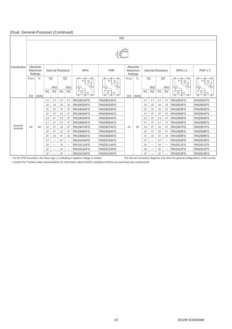
(Dual, General-Purpose) (Continued)
Classification
fS6
1.0
1.0
0.8
Absolute Maximum Ratings
Internal Resistors NPN PNPAbsolute Maximum Ratings
Internal Resistors NPN x 2 PNP x 2
VCEO IC Q1 Q2
Q1 Q2
R2
R2
R1
R1
Q1 Q2
R2
R2
R1
R1VCEO IC Q1 Q2
Q1 Q2
R2
R2
R1
R1
Q1 Q2
R2
R2
R1
R1
(kΩ) (kΩ) (kΩ) (kΩ)R1 R2 R1 R2 R1 R2 R1 R2
(V) (mA) (V) (mA)
General-purpose 50 80
4.7 4.7 4.7 4.7 RN1901AFS RN2901AFS
20 50
4.7 4.7 4.7 4.7 RN1901FS RN2901FS10 10 10 10 RN1902AFS RN2902AFS 10 10 10 10 RN1902FS RN2902FS22 22 22 22 RN1903AFS RN2903AFS 22 22 22 22 RN1903FS RN2903FS47 47 47 47 RN1904AFS RN2904AFS 47 47 47 47 RN1904FS RN2904FS2.2 47 2.2 47 RN1905AFS RN2905AFS 2.2 47 2.2 47 RN1905FS RN2905FS4.7 47 4.7 47 RN1906AFS RN2906AFS 4.7 47 4.7 47 RN1906FS RN2906FS10 47 10 47 RN1907AFS RN2907AFS 10 47 10 47 RN1907FS RN2907FS22 47 22 47 RN1908AFS RN2908AFS 22 47 22 47 RN1908FS RN2908FS47 22 47 22 RN1909AFS RN2909AFS 47 22 47 22 RN1909FS RN2909FS4.7 — 4.7 — RN1910AFS RN2910AFS 4.7 — 4.7 — RN1910FS RN2910FS10 — 10 — RN1911AFS RN2911AFS 10 — 10 — RN1911FS RN2911FS22 — 22 — RN1912AFS RN2912AFS 22 — 22 — RN1912FS RN2912FS47 — 47 — RN1913AFS RN2913AFS 47 — 47 — RN1913FS RN2913FS
x For the PNP transistors, the minus sign (–) indicating a negative voltage is omitted. The internal connection diagrams only show the general configurations of the circuits.
x Contact the Toshiba sales representative for information about RoHS compliance before you purchase any components.
10 2012/8 SCE0004M

(Dual, General-Purpose) (Continued)
Classification
fS6
1.0
1.0
0.8
Absolute Maximum Ratings
Internal Resistors NPN PNPAbsolute Maximum Ratings
Internal Resistors NPN x 2 PNP x 2
VCEO IC Q1 Q2
Q1 Q2
R2
R2
R1
R1
Q1 Q2
R2
R2
R1
R1VCEO IC Q1 Q2
Q1 Q2
R2
R2
R1
R1
Q1 Q2
R2
R2
R1
R1
(kΩ) (kΩ) (kΩ) (kΩ)R1 R2 R1 R2 R1 R2 R1 R2
(V) (mA) (V) (mA)
General-purpose 50 80
4.7 4.7 4.7 4.7 RN1901AFS RN2901AFS
20 50
4.7 4.7 4.7 4.7 RN1901FS RN2901FS10 10 10 10 RN1902AFS RN2902AFS 10 10 10 10 RN1902FS RN2902FS22 22 22 22 RN1903AFS RN2903AFS 22 22 22 22 RN1903FS RN2903FS47 47 47 47 RN1904AFS RN2904AFS 47 47 47 47 RN1904FS RN2904FS2.2 47 2.2 47 RN1905AFS RN2905AFS 2.2 47 2.2 47 RN1905FS RN2905FS4.7 47 4.7 47 RN1906AFS RN2906AFS 4.7 47 4.7 47 RN1906FS RN2906FS10 47 10 47 RN1907AFS RN2907AFS 10 47 10 47 RN1907FS RN2907FS22 47 22 47 RN1908AFS RN2908AFS 22 47 22 47 RN1908FS RN2908FS47 22 47 22 RN1909AFS RN2909AFS 47 22 47 22 RN1909FS RN2909FS4.7 — 4.7 — RN1910AFS RN2910AFS 4.7 — 4.7 — RN1910FS RN2910FS10 — 10 — RN1911AFS RN2911AFS 10 — 10 — RN1911FS RN2911FS22 — 22 — RN1912AFS RN2912AFS 22 — 22 — RN1912FS RN2912FS47 — 47 — RN1913AFS RN2913AFS 47 — 47 — RN1913FS RN2913FS
x For the PNP transistors, the minus sign (–) indicating a negative voltage is omitted. The internal connection diagrams only show the general configurations of the circuits.
x Contact the Toshiba sales representative for information about RoHS compliance before you purchase any components.
Classification
Absolute Maximum Ratings
Internal Resistors
ES6
VCEO IC Q1 Q21.6
1.6
1.2
(mm)NPN x 2 PNP x 2 NPN x 2 PNP x 2 PNP + NPN NPN + PNP NPN + PNP
Q1 Q2
R2
R2
R1
R1
Q1 Q2
R2
R2
R1
R1
R2
Q2Q1
R1
R2
R1R2
Q2Q1
R1
R2
R1
R1
R1
Q1
Q2
R2
R2
R1
R1
Q1
Q2
R2
R2
R2
Q2Q1
R1
R2
R1
(kΩ) (kΩ)
R1 R2 R1 R2
(V) (mA)
General-purpose 50 100
4.7 4.7 4.7 4.7 RN1901FE RN2901FE RN1961FE RN2961FE RN4901FE RN4981FE10 10 10 10 RN1902FE RN2902FE RN1962FE RN2962FE RN4902FE RN4982FE RN4962FE22 22 22 22 RN1903FE RN2903FE RN1963FE RN2963FE RN4903FE RN4983FE47 47 47 47 RN1904FE RN2904FE RN1964FE RN2964FE RN4904FE RN4984FE2.2 47 2.2 47 RN1905FE RN2905FE RN1965FE RN2965FE RN4905FE RN4985FE4.7 47 4.7 47 RN1906FE RN2906FE RN1966FE RN2966FE RN4906FE RN4986FE10 47 10 47 RN1907FE RN2907FE RN1967FE RN2967FE RN4907FE RN4987FE22 47 22 47 RN1908FE RN2908FE RN1968FE RN2968FE RN4908FE RN4988FE47 22 47 22 RN1909FE RN2909FE RN1969FE RN2969FE RN4909FE RN4989FE4.7 — 4.7 — RN1910FE RN2910FE RN1970FE RN2970FE RN4910FE RN4990FE10 — 10 — RN1911FE RN2911FE RN1971FE RN2971FE RN4911FE RN4991FE
x For the PNP transistors, the minus sign (–) indicating a negative voltage is omitted. The internal connection diagrams only show the general configurations of the circuits.
x Contact the Toshiba sales representative for information about RoHS compliance before you purchase any components.
11 2012/8 SCE0004M

(Dual, General-Purpose) (Continued)
Classification
Absolute Maximum Ratings
Internal Resistors
US6
VCEO IC Q1 Q22.0
2.1
1.25
(mm)NPN x 2 PNP x 2 NPN x 2 PNP x 2 PNP + NPN NPN + PNP
Q1 Q2
R2
R2
R1
R1
Q1 Q2
R2
R2
R1
R1
R2
Q2Q1
R1
R2
R1R2
Q2Q1
R1
R2
R1
R1
R1
Q1
Q2
R2
R2
R1
R1
Q1
Q2
R2
R2
(kΩ) (kΩ)R1 R2 R1 R2
(V) (mA)
General-purpose 50 100
4.7 4.7 4.7 4.7 RN1901 RN2901 RN1961 RN2961 RN4901 RN498110 10 10 10 RN1902 RN2902 RN1962 RN2962 RN4902 RN498222 22 22 22 RN1903 RN2903 RN1963 RN2963 RN4903 RN498347 47 47 47 RN1904 RN2904 RN1964 RN2964 RN4904 RN49842.2 47 2.2 47 RN1905 RN2905 RN1965 RN2965 RN4905 RN49854.7 47 4.7 47 RN1906 RN2906 RN1966 RN2966 RN4906 RN498610 47 10 47 RN1907 RN2907 RN1967 RN2967 RN4907 RN498722 47 22 47 RN1908 RN2908 RN1968 RN2968 RN4908 RN498847 22 47 22 RN1909 RN2909 RN1969 RN2969 RN4909 RN49894.7 — 4.7 — RN1910 RN2910 RN1970 RN2970 RN4910 RN499010 — 10 — RN1911 RN2911 RN1971 RN2971 RN4911 RN4991
x For the PNP transistors, the minus sign (–) indicating a negative voltage is omitted. The internal connection diagrams only show the general configurations of the circuits.
x Contact the Toshiba sales representative for information about RoHS compliance before you purchase any components.
12 2012/8 SCE0004M

(Dual, General-Purpose) (Continued)
Classification
Absolute Maximum Ratings
Internal Resistors
US6
VCEO IC Q1 Q22.0
2.1
1.25
(mm)NPN x 2 PNP x 2 NPN x 2 PNP x 2 PNP + NPN NPN + PNP
Q1 Q2
R2
R2
R1
R1
Q1 Q2
R2
R2
R1
R1
R2
Q2Q1
R1
R2
R1R2
Q2Q1
R1
R2
R1
R1
R1
Q1
Q2
R2
R2
R1
R1
Q1
Q2
R2
R2
(kΩ) (kΩ)R1 R2 R1 R2
(V) (mA)
General-purpose 50 100
4.7 4.7 4.7 4.7 RN1901 RN2901 RN1961 RN2961 RN4901 RN498110 10 10 10 RN1902 RN2902 RN1962 RN2962 RN4902 RN498222 22 22 22 RN1903 RN2903 RN1963 RN2963 RN4903 RN498347 47 47 47 RN1904 RN2904 RN1964 RN2964 RN4904 RN49842.2 47 2.2 47 RN1905 RN2905 RN1965 RN2965 RN4905 RN49854.7 47 4.7 47 RN1906 RN2906 RN1966 RN2966 RN4906 RN498610 47 10 47 RN1907 RN2907 RN1967 RN2967 RN4907 RN498722 47 22 47 RN1908 RN2908 RN1968 RN2968 RN4908 RN498847 22 47 22 RN1909 RN2909 RN1969 RN2969 RN4909 RN49894.7 — 4.7 — RN1910 RN2910 RN1970 RN2970 RN4910 RN499010 — 10 — RN1911 RN2911 RN1971 RN2971 RN4911 RN4991
x For the PNP transistors, the minus sign (–) indicating a negative voltage is omitted. The internal connection diagrams only show the general configurations of the circuits.
x Contact the Toshiba sales representative for information about RoHS compliance before you purchase any components.
Classification
Absolute Maximum Ratings
Internal Resistors
SM6
VCEO IC Q1 Q2 2.9
2.8
1.6
(mm)NPN x 2 PNP x 2 NPN x 2 PNP + NPN
Q1 Q2
R2
R2
R1
R1
Q1 Q2
R2
R2
R1
R1
R2
Q2Q1
R1
R2
R1
R1
R1
Q1
Q2
R2
R2
(kΩ) (kΩ)R1 R2 R1 R2
(V) (mA)
General-purpose 50 100
4.7 4.7 4.7 4.7 RN1601 RN2601 RN460110 10 10 10 RN1602 RN2602 RN460222 22 22 22 RN1603 RN2603 RN460347 47 47 47 RN1604 RN2604 RN46042.2 47 2.2 47 RN1605 RN2605 RN46054.7 47 4.7 47 RN1606 RN2606 RN460610 47 10 47 RN1607 RN2607 RN460722 47 22 47 RN1608 RN2608 RN460847 22 47 22 RN1609 RN2609 RN46094.7 — 4.7 — RN1610 RN2610 RN461010 — 10 — RN1611 RN2611 RN4611
x For the PNP transistors, the minus sign (–) indicating a negative voltage is omitted.
x Contact the Toshiba sales representative for information about RoHS compliance before you purchase any components.
The internal connection diagrams only show the general configurations of the circuits.
13 2012/8 SCE0004M
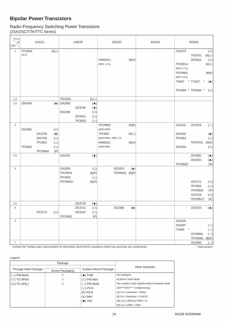
Bipolar Power Transistors
Radio-Frequency Switching Power Transistors(2SA/2SC/TTA/TTC Series)
VCEO
(V)IC(A)
10/(15) (18)/20 (25)/30 40/(45) 50/(60)
1 TPC6D02 (&)(r) 2SA2070 (7)(15 V) TPC6701 (W)(r)
HN4B101J (M)(V) 2SC5810 (7)(NPN: 1.2 A) TPC6901A (M)(r)
(PNP: 0.7 A)
TPCP8901 (M)(P)(PNP: 0.8 A)
TTA007 * TTC007 * (a)
TPC6604 * TPC6504 * (r)
1.2 TPC6D03 (&)(r)1.5 2SA2058 (a) 2SA2065 (a)
2SC5784 (a)
2SA2069 (7)
2SC5819 (7)
TPC6503 (r)2 TPCP8902 (M)(P) 2SA1241 2SC3076 (F)
2SA2066 (7) (NPN+PNP)
2SC5755 (a) TPC6902 (M)(r) 2SA2056 (a)
2SC5785 (7) (NPN+PNP) : PNP-1.7A TPC6601 (r)
TPC6501 (r) HN4B102J (M)(V) TPCP8701 (W)(P)
TPC6602 (r) (NPN+PNP) 2SA2060 (7)
TPCP8504 (P)2.5 2SA2061 (a) 2SC5692 (a)
2SC6033 (a)
TPCP8602 (P)3 2SA2059 (7) 2SC5976 (a)
TPCP8F01 ($)(P) TPCP8H02 ($)(P)
TPC6603 (r)
TPCP8G01* ($)(P) 2SC5712 (7)
TPC6502 (r)
TPCP8505 (P)
2SC6126 (7)
TPCP8511* (P)3.5 2SC5738 (a)4 2SC5714 (7) 2SC5906 (a) 2SC5703 (a)
2SC5713 (7) 2SC6125 (7)
TPCP8601 (P)5 2SA1244
2SA2097 (F)
TTA005 * (F)
2SC5886A (F)
TPCP8H01 ($)(P)7 2SC6000 (F)
x Contact the Toshiba sales representative for information about RoHS compliance before you purchase any components. *: New product
Legend
PackageOther Remarks
Through-Hole Package Surface-Mount PackageAmmo Packaging
(F) PW-Mold # (a) TSM (%) Darlington
(s) TO-3P(N) # (7) PW-Mini (#) Built-in zener diode
( ) TO-3P(L) # (F) PW-Mold Part number in italic signifies built in Freewheel diode.
(r) VS-6 2SA****/2SC****: Complementary
(P) PS-8 (&) 2-in-1 (transistor + diode)
(V) SMV ($) 2-in-1 (transistor + S-MOS)
(s) TFP (W) 2-in-1 (NPN (or PNP) × 2)
(M) 2-in-1 (NPN + PNP)
14 2012/8 SCE0004M

VCEO
(V)IC(A)
80 120 (140)/150 160 (180)/200
1 TPCP8507 (P)
TPCP8510 * (P)
2SC6061 (a)1.5 2SA1225 (F)2 2SA2206 2SC6124 (7)3 TTA003 (F)
2SC6076 (F)5 2SC3303 (F)
10 2SA1941 2SC5198 (s)
(140 V)
12 2SA1942 2SC5199 ( )
2SA2120 2SC5948 (s)
15 2SA2121 2SC5949 ( )18 TTA0001 * TTC0001 * (s)
TTA0002 * TTC0002 * ( )
VCEO
(V)IC(A)
230 300 (370)/400 (550)/600 800
0.05 2SC6127 (F)0.3 TPCP8604 (P)0.5 TTC013 * (7)
(350 V)
2SA1971 (7)2SA2142 (F)
0.8 2SC5458 (F)1 TTC011 * (@)
TTC005 * (7)(285 V)
2SA2184 (F)(550 V)
1.5 TTC008 * (F) 2SC6142 (F)(285 V) (375 V)
2 2SC5548A (F)2SA2034
TTC012 * (F)(375 V)
5 2SC5354 (s)12
15 2SA1943 2SC5200 ( )2SA1962 2SC5242 (s)
2SA1986 2SC5358 (s)
2SA1987 2SC5359 ( )TTA1943 * TTC5200 * ( )
x The products shown in bold are also manufactured in offshore fabs. *: New product
x Contact the Toshiba sales representative for information about RoHS compliance before you purchase any components.
Legend
PackageOther Remarks
Through-Hole Package Surface-Mount PackageAmmo Packaging
(F) PW-Mold # (a) TSM (%) Darlington
(s) TO-3P(N) # (7) PW-Mini (#) Built-in zener diode
( ) TO-3P(L) # (F) PW-Mold Part number in italic signifies built in Freewheel diode.
(r) VS-6 2SA****/2SC****: Complementary
(P) PS-8 (&) 2-in-1 (transistor + diode)
(V) SMV ($) 2-in-1 (transistor + S-MOS)
(s) TFP (W) 2-in-1 (NPN (or PNP) × 2)
(M) 2-in-1 (NPN + PNP)
15 2012/8 SCE0004M

Low-Frequency Power Transistors(2SB/2SD/TTB/TTD Series)
VCEO
(V)IC(A)
60/(65) 120
0.8 2SD2719 (#)(%)(a)0.9 TPCP8L01(1) (&)(P)
1 2SD2686 (#)(%)(7)3 2SB906 (F)
TTB001 * (s)
TTB002 * (F)
(1) NPN + HED (200 V/1 A) *: New product
x The products shown in bold are also manufactured in offshore fabs.
x Contact the Toshiba sales representative for information about RoHS compliance before you purchase any components.
Legend
PackageOther Remarks
Through-Hole Package Surface-Mount PackageAmmo Packaging
(F) PW-Mold # (a) TSM (%) Darlington
(s) TO-3P(N) # (7) PW-Mini (#) Built-in zener diode
( ) TO-3P(L) # (F) PW-Mold Part number in italic signifies built in Freewheel diode.
(r) VS-6 2SA****/2SC****: Complementary
(P) PS-8 (&) 2-in-1 (transistor + diode)
(V) SMV ($) 2-in-1 (transistor + S-MOS)
(s) TFP (W) 2-in-1 (NPN (or PNP) × 2)
(M) 2-in-1 (NPN + PNP)
16 2012/8 SCE0004M
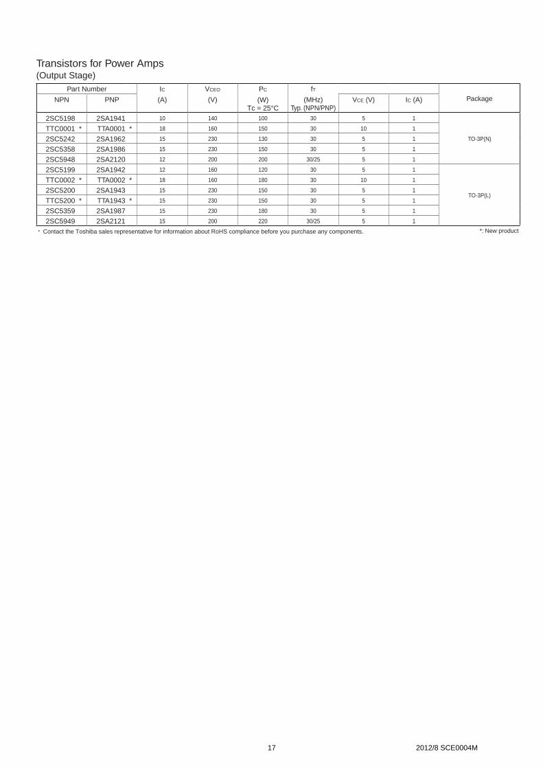
Transistors for Power Amps(Output Stage)
Part Number IC VCEO PC fTPackageNPN PNP (A) (V) (W)
Tc = 25°C(MHz)
Typ. (NPN/PNP)VCE (V) IC (A)
2SC5198 2SA1941 10 140 100 30 5 1
TO-3P(N)
TTC0001 * TTA0001 * 18 160 150 30 10 1
2SC5242 2SA1962 15 230 130 30 5 1
2SC5358 2SA1986 15 230 150 30 5 1
2SC5948 2SA2120 12 200 200 30/25 5 1
2SC5199 2SA1942 12 160 120 30 5 1
TO-3P(L)
TTC0002 * TTA0002 * 18 160 180 30 10 1
2SC5200 2SA1943 15 230 150 30 5 1
TTC5200 * TTA1943 * 15 230 150 30 5 1
2SC5359 2SA1987 15 230 180 30 5 1
2SC5949 2SA2121 15 200 220 30/25 5 1
x Contact the Toshiba sales representative for information about RoHS compliance before you purchase any components. *: New product
17 2012/8 SCE0004M
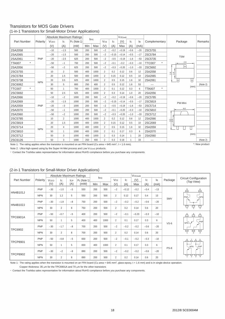
Transistors for MOS Gate Drivers(1-in-1 Transistors for Small-Motor Driver Applications)
Part Number Polarity
Absolute Maximum RatingshFE
VCE(sat)
Complementary Package RemarksVCEO IC PC (Note 1) VCE IC (V) IC IB
(V) (A) (mW) Min Max (V) (A) Max (A) (mA)
2SA2058
PNP
–10 –1.5 500 200 500 –2 –0.2 –0.19 –0.6 –20 2SC5755
TSM
2.9
2.8
1.6
(mm)
2SA2065 –20 –1.5 500 200 500 –2 –0.15 –0.14 –0.5 –17 2SC5784
2SA2061 –20 –2.5 625 200 500 –2 –0.5 –0.19 –1.6 –53 2SC5735
TTA007 * –50 –1 700 200 500 –2 –0.1 –0.2 –0.3 –10 TTC007 *
2SA2056 –50 –2 625 200 500 –2 –0.3 –0.20 –1.0 –33 2SC5692
2SC5755
NPN
10 2 500 400 1000 2 0.2 0.12 0.6 12 2SA2058
2SC5784 20 1.5 500 400 1000 2 0.15 0.12 0.5 10 2SA2065
2SC5738 20 3.5 625 400 1000 2 0.5 0.15 1.6 32 2SA2061
2SC6062 30 5 800 250 400 2 0.5 0.12 1.6 53 — (Note 2)
TTC007 * 50 1 700 400 1000 2 0.1 0.12 0.3 6 TTA007 *
2SC5692 50 2.5 625 400 1000 2 0.3 0.14 1.0 20 2SA2056
2SA2066
PNP
–10 –2 1000 200 500 –2 –0.2 –0.19 –0.6 –20 2SC5785
PW-Mini
4.6
4.2
2.5
(mm)
2SA2069 –20 –1.5 1000 200 500 –2 –0.15 –0.14 –0.5 –17 2SC5819
2SA2059 –20 –3 1000 200 500 –2 –0.5 –0.19 –1.6 –53 2SC5714
2SA2070 –50 –1 1000 200 500 –2 –0.1 –0.20 –0.3 –10 2SC5810
2SA2060 –50 –2 1000 200 500 –2 –0.3 –0.20 –1.0 –33 2SC5712
2SC5785
NPN
10 2 1000 400 1000 2 0.2 0.12 0.6 12 2SA2066
2SC5819 20 1.5 1000 400 1000 2 0.15 0.12 0.5 10 2SC2069
2SC5714 20 4 1000 400 1000 2 0.5 0.15 1.6 32 2SA2059
2SC5810 50 1 1000 400 1000 2 0.1 0.17 0.3 6 2SA2070
2SC5712 50 3 1000 400 1000 2 0.3 0.14 1 20 2SA2060
2SC6126 50 3 1000 250 400 2 0.3 0.18 1 33 — (Note 2)
Note 1: The rating applies when the transistor is mounted on an FR4 board (Cu area = 645 mm2, t = 1.6 mm). *: New product
Note 2: Ultra-high-speed using by the Super Hi-Met process and Low VCE(sat) products.
x Contact the Toshiba sales representative for information about RoHS compliance before you purchase any components.
(2-in-1 Transistors for Small-Motor Driver Applications)
Part Number Polarity
Absolute Maximum RatingshFE
VCE(sat)
PackageCircuit Configuration
(Top View)VCEO
(V)IC(A)
ICP
(A)PC (Note 1)
(mW)VCE IC (V) IC IB
Min Max (V) (A) Max (A) (mA)
HN4B101JPNP –30 –1.0 –5 550 200 500 –2 –0.12 –0.2 –0.4 –13
SMVPNP NPN
1
45
2 3
NPN 30 1.2 5 550 200 500 2 0.12 0.17 0.4 13
HN4B102JPNP –30 –1.8 –8 750 200 500 –2 –0.2 –0.2 –0.6 –20
NPN 30 2 8 750 200 500 2 0.2 0.14 0.6 20
TPC6901APNP –50 –0.7 –5 400 200 500 –2 –0.1 –0.23 –0.3 –10
VS-6PNP
NPN
1
456
2 3
NPN 50 1 5 400 400 1000 2 0.1 0.17 0.3 6
TPC6902PNP –30 –1.7 –8 700 200 500 –2 –0.2 –0.2 –0.6 –20
NPN 30 2 8 700 200 500 2 0.2 0.14 0.6 20
TPCP8901PNP –50 –0.8 –5 830 200 500 –2 –0.1 –0.2 –0.3 –10
PS-8PNPNPN
1
5678
2 3 4
NPN 50 1 5 830 400 1000 2 0.1 0.17 0.3 6
TPCP8902PNP –30 –2 –8 890 200 500 –2 –0.2 –0.2 –0.6 –20
NPN 30 2 8 890 200 500 2 0.2 0.14 0.6 20
Note 1: The rating applies when the transistor is mounted on an FR4 board (Cu area = 645 mm2, glass-epoxy, t = 1.6 mm) and is in single-device operation.
Copper thickness: 35 mm for the TPC6901A and 70 mm for the other transistors
x Contact the Toshiba sales representative for information about RoHS compliance before you purchase any components.
18 2012/8 SCE0004M
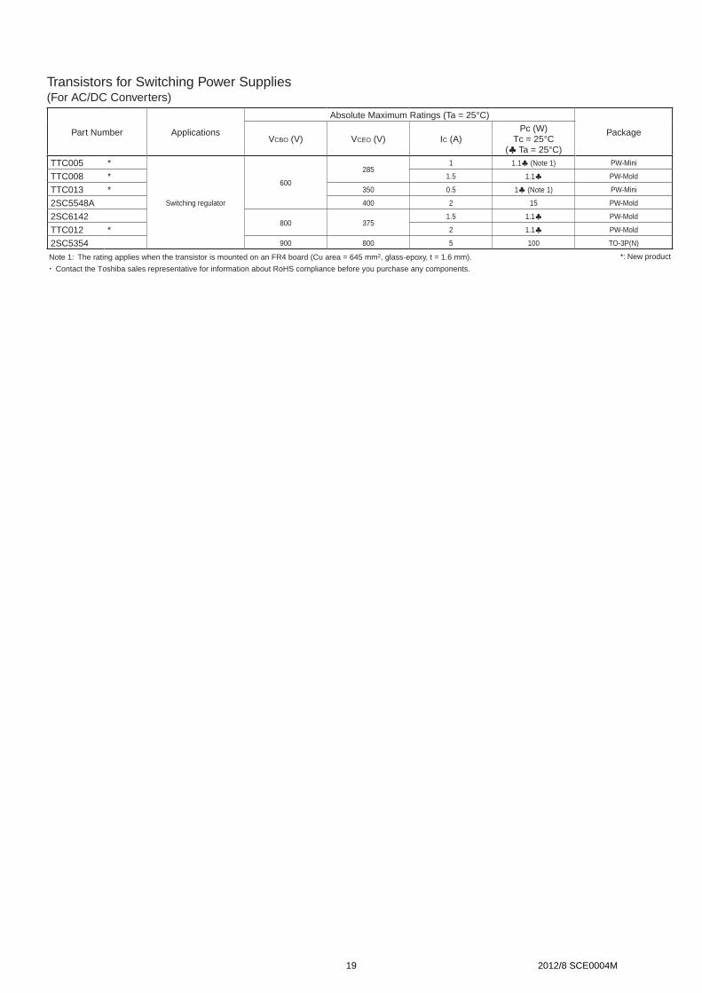
Transistors for Switching Power Supplies(For AC/DC Converters)
Part Number Applications
Absolute Maximum Ratings (Ta = 25°C)
PackageVCBO (V) VCEO (V) IC (A)
Pc (W)Tc = 25°C
(d Ta = 25°C)
TTC005 *
Switching regulator
600
2851 1.1d (Note 1) PW-Mini
TTC008 * 1.5 1.1d PW-Mold
TTC013 * 350 0.5 1d (Note 1) PW-Mini
2SC5548A 400 2 15 PW-Mold
2SC6142800 375
1.5 1.1d PW-Mold
TTC012 * 2 1.1d PW-Mold
2SC5354 900 800 5 100 TO-3P(N)
Note 1: The rating applies when the transistor is mounted on an FR4 board (Cu area = 645 mm2, glass-epoxy, t = 1.6 mm). *: New product
x Contact the Toshiba sales representative for information about RoHS compliance before you purchase any components.
19 2012/8 SCE0004M

Transistors for High-Voltage Power Supplies(For DC/DC Converters)
Part Number
Absolute Maximum Ratings hFE VCE(sat) (V)
PackageVCEX(V) VCEO(V) IC(A) PC (W) VCE(V) IC(A) IC(A) IB(mA)
Min Max Max
2SC6061 150 120 1 0.625 (Note 1) 120 300 2 0.1 0.14 0.3 10 TSM
TPCP8510 * 150 120 1 1.1 (Note 1) 120 300 2 0.1 0.14 0.3 10 PS-8
TPCP8507 150 120 1 1.25 (Note 1) 120 300 2 0.1 0.14 0.3 10 PS-8
2SC6076 160 80 3 10 (Note 2) 180 450 2 0.5 0.5 1 100 PW-Mold
2SC6124 160 80 2 1 (Note 1) 100 200 2 0.5 0.5 1 100 PW-Mini
Note 1: The rating applies when the transistor is mounted on an FR4 board (Cu area = 645 mm2, glass-epoxy, t = 1.6 mm). *: New product
Note 2: Tc = 25°C
x Contact the Toshiba sales representative for information about RoHS compliance before you purchase any components.
(Transistors for Droppers)
Part Number
Absolute Maximum Ratings hFE VCE(sat)(V)
PackageVCEO(V) IC(A)
PC (W) Tc = 25°C
VCE(V) IC(A) IC(A) IB(mA)Min Max Max
2SB906 –60 –3 20 60 200 –5 –0.5 –1.7 –3 –300 PW-Mold
TTB001 * –60 –3 36 100 250 –5 –0.5 –1.7 –3 –300 TFP
TTB002 * –60 –3 30 100 250 –5 –0.5 –1.7 –3 –300 PW-Mold
TTA005 * –50 –5 24 200 500 –2 –0.5 –0.27 –1.6 –53 PW-Mold
x Contact the Toshiba sales representative for information about RoHS compliance before you purchase any components. *: New product
(High-Voltage Transistors)
Part NumberAbsolute Maximum Ratings
PackageCircuit Configuration
(Top View)Remarks
VCEO(V) IC(A) PC(W)
2SA1971 –400 –0.5 1 PW-Mini TPCP8604
PNP
1
5678
2 3 4
TPCP8604 –400 –0.3 1 PS-8 SMD
2SA2184 –550 –1 1 PW-Mold SMD only
2SA2142 –600 –0.5 10 PW-Mold SMD only
2SC6127 800 0.05 10 PW-Mold SMD only
x The circuit configuration diagrams only show the general configurations of the circuits.
x Contact the Toshiba sales representative for information about RoHS compliance before you purchase any components.
20 2012/8 SCE0004M

Low Saturation Voltage Transistors(Small Surface-Mount Packages for Personal Equipments)
Part Number ConfigurationAbsolute Maximum Ratings hFE VCE(sat) (V)
Marking PackageVCEO(V) IC(A) ICP(A)
Pc(mW) (Note 1)
Pc(mW) (Note 1)t = 10 s
VCE(V) IC(A) IC(A) IB(mA)Min Max Max
2SA2058
PNP single
–10 –1.5 –2.5 500 750 200 500 –2 –0.2 –0.19 –0.6 –20 WM
TSM
equivalent to
SC-59SOT-23
2SA2065 –20 –1.5 –2.5 500 750 200 500 –2 –0.15 –0.14 –0.5 –17 WK
2SA2061 –20 –2.5 –4 625 1000 200 500 –2 –0.5 –0.19 –1.6 –53 WE
TTA007 * –50 –1 –2 700 1100 200 500 –2 –0.1 –0.2 –0.3 –10 WH
2SA2056 –50 –2 –3.5 625 1000 200 500 –2 –0.3 –0.20 –1.0 –33 WF
2SC5755
NPN single
10 2 3.5 500 750 400 1000 2 0.2 0.12 0.6 12 WL
2SC5784 20 1.5 2.5 500 750 400 1000 2 0.15 0.12 0.5 10 WJ
2SC5738 20 3.5 6 625 1000 400 1000 2 0.5 0.15 1.6 32 WD
2SC5976 30 3 5 625 1000 250 400 2 0.3 0.14 1.0 33 WW
2SC5906 30 4 7 800 1250 200 500 2 0.5 0.2 1.6 53 WP
TTC007 * 50 1 2 700 1100 400 1000 2 0.1 0.12 0.3 6 WG
2SC5692 50 2.5 4 625 1000 400 1000 2 0.3 0.14 1.0 20 WB
2SC6033 50 2.5 5 625 1000 250 400 2 0.3 0.18 1.0 33 WX
2SC5703 50 4 7 800 1250 400 1000 2 0.5 0.12 1.6 32 WA
2SC6061 120 1 2 625 1000 120 300 2 0.1 0.14 0.3 10 WN
HN4B101JPNP + NPN
±30 –1/1.2 ±5 550 850 200 500 ±2 ±0.12 –0.2/0.17 ±0.4 ±13 5KSMV
HN4B102J ±30 –1.8/2 ±8 750 750 200 500 ±2 ±0.2 –0.2/0.14 ±0.6 ±20 5L
2SA2066
PNP single
–10 –2 –3.5 1000 2000 200 500 –2 –0.2 –0.19 –0.6 –20 4E
2SA2069 –20 –1.5 –2.5 1000 2000 200 500 –2 –0.15 –0.14 –0.5 –17 4D
2SA2059 –20 –3 –5 1000 2500 200 500 –2 –0.5 –0.19 –1.6 –53 4F
2SA2070 –50 –1 –2 1000 2000 200 500 –2 –0.1 –0.2 –0.3 –10 4C
2SA2060 –50 –2 –3.5 1000 2500 200 500 –2 –0.3 –0.20 –1.0 –33 4G
2SA2206 –80 –2 –4 1000 2500 100 200 –2 –0.5 –0.5 –1.0 –100 4K PW-Mini
2SC5785
NPN single
10 2 3.5 1000 2000 400 1000 2 0.2 0.12 0.6 12 3E equivalent to
SC-62SOP-89
2SC5713 10 4 7 1000 2500 400 1000 2 0.5 0.15 1.6 32 2C
2SC5819 20 1.5 2.5 1000 2000 400 1000 2 0.15 0.12 0.5 10 3D
2SC6125 20 4 8 1000 2500 180 390 2 0.5 0.2 1.6 53 4L
2SC5714 20 4 7 1000 2500 400 1000 2 0.5 0.15 1.6 32 2E
2SC5810 50 1 2 1000 2000 400 1000 2 0.1 0.17 0.3 6 3C
2SC6126 50 3 6 1000 2500 250 400 2 0.3 0.18 1.0 33 4M
2SC5712 50 3 5 1000 2500 400 1000 2 0.3 0.14 1 20 2A
2SC6124 80 2 4 1000 2500 100 200 2 0.5 0.5 1.0 100 4J
TPC6501
NPN single
10 2 3.5 800 1600 400 1000 2 0.2 0.12 0.6 12 H2A
VS-6(equivalent to
TSOP-6)
TPC6502 50 3 5 800 1600 400 1000 2 0.3 0.14 1 20 H2B
TPC6503 20 1.5 2.5 800 1600 400 1000 2 0.15 0.12 0.5 10 H2C
TPC6504 * 50 1 2 800 1600 400 1000 2 0.1 0.17 0.3 6 H2D
TPC6601
PNP single
–50 –2 –3.5 800 1600 200 500 –2 –0.3 –0.20 –1.0 –33 H3A
TPC6602 –10 –2 –3.5 800 1600 200 500 –2 –0.2 –0.19 –0.6 –20 H3B
TPC6603 –20 –3 –5 800 1600 200 500 –2 –0.5 –0.19 –1.6 –53 H3C
TPC6604 * –50 –1 –2 800 1600 200 500 –2 –0.1 –0.23 –0.3 –10 H3D
TPC6701 NPN/dual 50 1 2 660 (Note 2) — 400 1000 2 0.1 0.17 0.3 6 H4A
TPC6901APNP + NPN
±50 –0.7/1.0 ±5 400 500 200/400 500/1000 ±2 ±0.1 –0.23/0.17 ±0.3 –10/6 H6B
TPC6902 ±30 –1.7/2 ±8 700 1000 200 500 ±2 ±0.2 –0.2/0.14 ±0.6 ±20 H6C
Note 1: The rating applies when the transistor is mounted on an FR4 board (Cu area = 645 mm2, glass-epoxy, t = 1.6 mm). *: New product
Note 2: Total loss of dual-device operation
x Contact the Toshiba sales representative for information about RoHS compliance before you purchase any components.
21 2012/8 SCE0004M

Low Saturation Voltage Transistors(Small Surface-Mount Packages for Personal Equipments) (Continued)
Part Number ConfigurationAbsolute Maximum Ratings hFE VCE(sat) (V)
Marking PackageVCEO(V) IC(A) ICP(A)
PC(mW) (Note 1)
PC(mW) (Note 1)t = 10 s
VCE(V) IC(A) IC(A) IB(mA)Min Max Max
2SA2097
PNP single
–50 –5 –10 20 (Note 3) — 200 500 –2 –0.5 –0.27 –1.6 –53 A2097
PW-MoldSC-63
TTA005 * –50 –5 –10 24 (Note 3) — 200 500 –2 –0.5 –0.27 –1.6 –53 A005
2SA1241 –50 –2 –3 10 (Note 3) — 70 240 –2 –0.5 –0.5 –1 –50 A1241
2SA1244 –50 –5 –8 20 (Note 3) — 70 240 –1 –1 –0.4 –3 –150 A1244
TTA003 * –80 –3 –5 10 (Note 3) — 100 200 –2 –0.5 –0.5 –1 –100 A003
2SC6076
NPN single
80 3 5 10 (Note 3) — 180 450 2 0.5 0.5 1 100 C6076
2SC5886A 50 5 10 20 (Note 3) — 400 1000 2 0.5 0.22 1.6 32 C5886A
2SC3076 50 2 3 10 (Note 3) — 70 240 2 0.5 0.5 1 50 C3076
2SC3303 80 5 8 20 (Note 3) — 70 240 1 1 0.4 3 150 C3303
2SC6000 50 7 10 20 (Note 3) — 250 400 2 2.5 0.18 2.5 83 C6000
TPCP8507
NPN single
120 1 2 1250 3000 120 300 2 0.1 0.14 0.3 10 8507
PS-8
TPCP8510 * 120 1 2 1100 2250 120 300 2 0.1 0.14 0.3 10 8510
TPCP8511 * 50 3 5 1250 3000 250 400 2 0.3 0.18 1 33 8511
TPCP8505 50 3 5 1250 3000 400 1000 2 0.3 0.14 1 20 8505
TPCP8504 10 2 3.5 1200 2800 400 1000 2 0.2 0.12 0.6 12 8504
TPCP8601PNP single
–20 –4 –7 1300 3300 200 500 –2 –0.6 –0.19 –2 –67 8601
TPCP8602 –50 –2.5 –4 1250 3000 200 500 –2 –0.3 –0.2 –1 –33 8602
TPCP8701 NPN/dual 50 3 5 940 1770 400 1000 2 0.3 0.14 1 20 8701
TPCP8H01 (Note 2) NPN+S-MOS
50 5 7 1000 2000 250 400 2 0.5 0.13 1.6 53 8H01
TPCP8H02 (Note 2) 30 3 5 1000 2000 250 400 2 0.3 0.14 1 33 8H02
TPCP8F01 (Note 2) PNP+S-MOS –20 –3 –5 1000 — 200 500 –2 –0.5 –0.19 –1.6 –53 8F01
TPCP8901PNP + NPN
±50 –0.8/1.0 ±5 830 1480 200/400 500/1000 ±2 ±0.1 –0.2/0.17 ±0.3 –10/6 8901
TPCP8902 ±30 ±2 ±8 890 1670 200 500 ±2 ±0.2 –0.2/0.14 ±0.6 ±20 8902
TPCP8L01 (Note 4)NPN
Darlington + HED
120 0.9 2 900 — 2000 9000 2 1 1.5 1 1 8L01
TPCP8G01 (Note 5) * PNP + Pch –20 –3 –5 940 1770 200 500 –2 –0.5 –0.19 –1.6 –53 8G01
Note 1: The rating applies when the transistor is mounted on an FR4 board (Cu area = 645 mm2, glass-epoxy, t = 1.6 mm). *: New product
Note 2: Built-in SBD, VRRM = 30 V, IO = 0.7 A, VF = 0.4 V (MAX)@IF = 0.5 A, IR = 100 mA (MAX)@VR = 10 V
Note 3: Tc = 25°C
Note 4: Built-in HED, VRRM = 200 V, IF(AV) = 1 A
Note 5: Pch MOS VDSS = –20 V, ID = –2 A, RON = 130 mΩ Max
x Contact the Toshiba sales representative for information about RoHS compliance before you purchase any components.
22 2012/8 SCE0004M
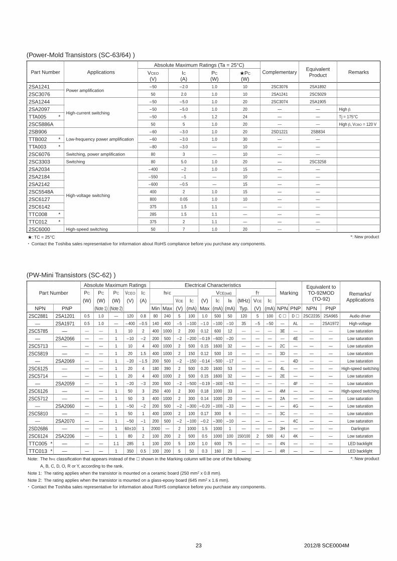
(Power-Mold Transistors (SC-63/64) )
Part Number ApplicationsAbsolute Maximum Ratings (Ta = 25°C)
ComplementaryEquivalent
ProductRemarksVCEO
(V)IC(A)
PC
(W)zPC
(W)
2SA1241Power amplification
–50 –2.0 1.0 10 2SC3076 2SA1892
2SC3076 50 2.0 1.0 10 2SA1241 2SC5029
2SA1244
High-current switching
–50 –5.0 1.0 20 2SC3074 2SA1905
2SA2097 –50 –5.0 1.0 20 — — High b
TTA005 * –50 –5 1.2 24 — — Tj = 175°C
2SC5886A 50 5 1.0 20 — — High b, VCBO = 120 V
2SB906Low-frequency power amplification
–60 –3.0 1.0 20 2SD1221 2SB834
TTB002 * –60 –3.0 1.0 30 — —
TTA003 * –80 –3.0 — 10 — —
2SC6076 Switching, power amplification 80 3 — 10 — —
2SC3303 Switching 80 5.0 1.0 20 — 2SC3258
2SA2034
High-voltage switching
–400 –2 1.0 15 — —
2SA2184 –550 –1 — 10 — —
2SA2142 –600 –0.5 — 15 — —
2SC5548A 400 2 1.0 15 — —
2SC6127 800 0.05 1.0 10 — —
2SC6142 375 1.5 1.1 — — —
TTC008 * 285 1.5 1.1 — — —
TTC012 * 375 2 1.1 — — —
2SC6000 High-speed switching 50 7 1.0 20 — —
z: TC = 25°C *: New product
x Contact the Toshiba sales representative for information about RoHS compliance before you purchase any components.
(PW-Mini Transistors (SC-62) )
Part Number
Absolute Maximum Ratings Electrical Characteristics
MarkingEquivalent to TO-92MOD
(TO-92)Remarks/
ApplicationsPC PC PC VCEO IC hFE VCE(sat) fT
(W) (W) (W) (V) (A) VCE IC (V) IC IB (MHz) VCE IC
NPN PNP (Note 1) (Note 2) Min Max (V) (mA) Max (mA) (mA) Typ. (V) (mA) NPN PNP NPN PNP
2SC2881 2SA1201 0.5 1.0 — 120 0.8 80 240 5 100 1.0 500 50 120 5 100 C D 2SC2235 2SA965 Audio driver
— 2SA1971 0.5 1.0 — –400 –0.5 140 400 –5 –100 –1.0 –100 –10 35 –5 –50 — AL — 2SA1972 High-voltage
2SC5785 — — — 1 10 2 400 1000 2 200 0.12 600 12 — — — 3E — — — Low saturation
— 2SA2066 — — 1 –10 –2 200 500 –2 –200 –0.19 –600 –20 — — — — 4E — — Low saturation
2SC5713 — — — 1 10 4 400 1000 2 500 0.15 1600 32 — — — 2C — — — Low saturation
2SC5819 — — — 1 20 1.5 400 1000 2 150 0.12 500 10 — — — 3D — — — Low saturation
— 2SA2069 — — 1 –20 –1.5 200 500 –2 –150 –0.14 –500 –17 — — — — 4D — — Low saturation
2SC6125 — — — 1 20 4 180 390 2 500 0.20 1600 53 — — — 4L — — — High-speed switching
2SC5714 — — — 1 20 4 400 1000 2 500 0.15 1600 32 — — — 2E — — — Low saturation
— 2SA2059 — — 1 –20 –3 200 500 –2 –500 –0.19 –1600 –53 — — — — 4F — — Low saturation
2SC6126 — — — 1 50 3 250 400 2 300 0.18 1000 33 — — — 4M — — — High-speed switching
2SC5712 — — — 1 50 3 400 1000 2 300 0.14 1000 20 — — — 2A — — — Low saturation
— 2SA2060 — — 1 –50 –2 200 500 –2 –300 –0.20 –1000 –33 — — — — 4G — — Low saturation
2SC5810 — — — 1 50 1 400 1000 2 100 0.17 300 6 — — — 3C — — — Low saturation
— 2SA2070 — — 1 –50 –1 200 500 –2 –100 –0.2 –300 –10 — — — — 4C — — Low saturation
2SD2686 — — — 1 60±10 1 2000 — 2 1000 1.5 1000 1 — — — 3H — — — Darlington
2SC6124 2SA2206 — — 1 80 2 100 200 2 500 0.5 1000 100 150/100 2 500 4J 4K — — Low saturation
TTC005 * — — — 1.1 285 1 100 200 5 100 1.0 600 75 — — — 4N — — — LED backlight
TTC013 * — — — 1 350 0.5 100 200 5 50 0.3 160 20 — — — 4R — — — LED backlight
Note: The hFE classification that appears instead of the shown in the Marking column will be one of the following: *: New product
A, B, C, D, O, R or Y, according to the rank.
Note 1: The rating applies when the transistor is mounted on a ceramic board (250 mm2 x 0.8 mm).
Note 2: The rating applies when the transistor is mounted on a glass-epoxy board (645 mm2 x 1.6 mm).
x Contact the Toshiba sales representative for information about RoHS compliance before you purchase any components.
23 2012/8 SCE0004M

Low Saturation Voltage Transistors(TSM Transistors)
Part Number Absolute Maximum Ratings hFE VCE(sat)(V)
MarkingRemarks/
ApplicationsNPN VCEO(V) IC(A) ICP(A)PC(mW) (Note 1)
PC(mW) (Note 1) t=10s
VCE(V) IC(A) IC(A) IB(mA)Min Max Max
2SA2058 –10 –1.5 –2.5 500 750 200 500 –2 –0.2 –0.19 –0.6 –20 WM Low saturation
2SA2065 –20 –1.5 –2.5 500 750 200 500 –2 –0.15 –0.14 –0.5 –17 WK Low saturation
2SA2061 –20 –2.5 –4 625 1000 200 500 –2 –0.5 –0.19 –1.6 –53 WE Low saturation
TTA007 * –50 –1 –2 700 1100 200 500 –2 –0.1 –0.2 –0.3 –10 WH Low saturation
2SA2056 –50 –2 –3.5 625 1000 200 500 –2 –0.3 –0.20 –1.0 –33 WF Low saturation
2SC5755 10 2 3.5 500 750 400 1000 2 0.2 0.12 0.6 12 WL Low saturation
2SC5784 20 1.5 2.5 500 750 400 1000 2 0.15 0.12 0.5 10 WJ Low saturation
2SC5738 20 3.5 6 625 1000 400 1000 2 0.5 0.15 1.6 32 WD Low saturation
2SC5976 30 3 5 625 1000 250 400 2 0.3 0.14 1.0 33 WW
Ultra-high-speed switching
Low saturation voltage
2SC5906 30 4 7 800 1250 200 500 2 0.5 0.2 1.6 53 WP
Ultra-high-speed switching
Low saturation voltage
TTC007 * 50 1 2 700 1100 400 1000 2 0.1 0.12 0.3 6 WG Low saturation
2SC5692 50 2.5 4 625 1000 400 1000 2 0.3 0.14 1.0 20 WB Low saturation
2SC6033 50 2.5 5 625 1000 250 400 2 0.3 0.18 1.0 33 WX
Ultra-high-speed switching
Low saturation voltage
2SC5703 50 4 7 800 1250 400 1000 2 0.5 0.12 1.6 32 WA Low saturation
2SD2719 60±10 0.8 3 800 1250 2000 — 2 1.0 1.5 1 1 WV Darlington
2SC6061 120 1 2 625 1000 120 300 2 0.1 0.14 0.3 10 WN Low saturation
Note 1: The rating applies when the transistor is mounted on an FR4 board (Cu area = 645 mm2, glass-epoxy, t = 1.6 mm). *: New product
x Contact the Toshiba sales representative for information about RoHS compliance before you purchase any components.
24 2012/8 SCE0004M

Junction FETs
Junction FETs(Surface-Mount Type)
ClassificationVGDS(V)
MaxIG(mA)Max
IDSS(mA) | Yfs | (mS) Min
S-MINI (SC-59) USM (SC-70)
Nch Pch Nch Pch
General-purpose
–50 10 0.3 to 6.5 1.2 2SK208 2SK879
50 –10 –1.2 to –14 1 2SJ106 2SJ144
–50 10 1.2 to 14 4 2SK209 — 2SK880 — x Contact the Toshiba sales representative for information about RoHS compliance before you purchase any components.
(Surface-Mount Type) (Electret Condense Microphone)
CharacteristicsVGDS(V)
MaxIG(mA)Max
IDSS Rank(mA)
| Yfs | (mS) Min
Ciss (pF)Typ.
VESM
Very Low NoiseSmall Ciss –20 10
A = 140 to 2400.9 1.8 TTK101MFV
B = 210 to 350
High gain –20 10A = 140 to 280
1.0 4.0 TTK501MFVB = 240 to 450
x Contact the Toshiba sales representative for information about RoHS compliance before you purchase any components.
Junction FETs (Dual)(Surface-Mount Type)
Classification VGDS(V) IG(mA) IDSS(mA) | Yfs | (mS) Min
SMV USVInternal Connections
Nch x 2 Pch x 2 Nch x 2 Pch x 2
General-purpose –50 10 1.2 to 14 4 2SK2145 — 2SK3320 — Q2Q1
x Contact the Toshiba sales representative for information about RoHS compliance before you purchase any components.
The internal connection diagrams only show the general configurations of the circuits.
Combination Products of Different Type Devices
Combination Products of Different Type Devices
FeaturesComponent
DevicesRatings
SM6 Internal ConnectionsBreakdown Voltage (V) Current (mA)
High breakdown voltage PNP Q1 2SA1587 VCEO –120 IC –100
HN2E04F
IndependentPNP + small-signal diode
Q1 Q2
Standard high-speed switching Q2 1SS352 VR 80 IO 100
The internal connection diagrams only show the general configurations of the circuits.
Package Lineup
S-MINI (SC-59)2.9
2.5
1.5
(mm)
USM (SC-70)2.0
2.1
1.25
(mm)
VESM
1.2
1.2
0.8
(mm)
SMV2.9
2.8
1.6
(mm)
USV
2.0
2.1
1.25
(mm)
SM62.9
2.8
1.6
(mm)
25 2012/8 SCE0004M

MOSFETs
Small-Signal MOSFETs (Single-Type)
Pol
arity
Absolute Maximum Ratings
Package
VDSS
(V)VGSS
(V)ID
(mA)
CST3 VESM SSM USM (SC-70) UFM S-MINI (SC-59)
0.6
0.350.38
1.0
1.2
1.2
0.8
1.6
1.6
0.8
2.0
2.1
1.25
2.0
2.1
1.7
2.9
2.5
1.5
(mm) (mm) (mm) (mm) (mm) (mm)
Nch
20 ±10 200 SSM3K37CT * SSM3K37FS *
20 ±10 250 SSM3K37MFV *
20 ±10 100 SSM3K16FU
20 ±10 180 SSM3K35CT SSM3K35MFV SSM3K35FS
20 ±10 500 SSM3K36MFV SSM3K36FS SSM3K36TU
20 ±10 500 SSM3K43FS # *
30 ±20 100 SSM3K15F
30 ±20 100 SSM3K15ACT * SSM3K15AMFV * SSM3K15AFS * SSM3K15AFU *
30 ±20 100 SSM3K44MFV # * SSM3K44FS # *
30 ±20 200 2SK2009
30 ±20 400 SSM3K09FU
50 ±7 100 SSM3K17FU
60 ±20 200 SSM3K7002BFS * SSM3K7002BFU * SSM3K7002BF *
60 ±20 200 2SK1062
Pch
–20 ±8 –330 SSM3J36MFV SSM3J36FS SSM3J36TU
–20 ±10 –100 SSM3J16CT SSM3J16FV SSM3J16FS SSM3J16FU
–20 ±10 –100 SSM3J35CT SSM3J35MFV SSM3J35FS
–30 ±20 –100 SSM3J15CT SSM3J15FV SSM3J15FS SSM3J15FU SSM3J15F
–30 ±20 –200 2SJ305
–30 ±20 –200 SSM3J09FU
–50 –7 –50 2SJ344 2SJ343
–60 ±20 –200 2SJ168
#: High ESD protection
x Contact the Toshiba sales representative for information about RoHS compliance before you purchase any components.
26 2012/8 SCE0004M

MOSFETs
Small-Signal MOSFETs (Single-Type)
Pol
arity
Absolute Maximum Ratings
Package
VDSS
(V)VGSS
(V)ID
(mA)
CST3 VESM SSM USM (SC-70) UFM S-MINI (SC-59)
0.6
0.350.38
1.0
1.2
1.2
0.8
1.6
1.6
0.8
2.0
2.1
1.25
2.0
2.1
1.7
2.9
2.5
1.5
(mm) (mm) (mm) (mm) (mm) (mm)
Nch
20 ±10 200 SSM3K37CT * SSM3K37FS *
20 ±10 250 SSM3K37MFV *
20 ±10 100 SSM3K16FU
20 ±10 180 SSM3K35CT SSM3K35MFV SSM3K35FS
20 ±10 500 SSM3K36MFV SSM3K36FS SSM3K36TU
20 ±10 500 SSM3K43FS # *
30 ±20 100 SSM3K15F
30 ±20 100 SSM3K15ACT * SSM3K15AMFV * SSM3K15AFS * SSM3K15AFU *
30 ±20 100 SSM3K44MFV # * SSM3K44FS # *
30 ±20 200 2SK2009
30 ±20 400 SSM3K09FU
50 ±7 100 SSM3K17FU
60 ±20 200 SSM3K7002BFS * SSM3K7002BFU * SSM3K7002BF *
60 ±20 200 2SK1062
Pch
–20 ±8 –330 SSM3J36MFV SSM3J36FS SSM3J36TU
–20 ±10 –100 SSM3J16CT SSM3J16FV SSM3J16FS SSM3J16FU
–20 ±10 –100 SSM3J35CT SSM3J35MFV SSM3J35FS
–30 ±20 –100 SSM3J15CT SSM3J15FV SSM3J15FS SSM3J15FU SSM3J15F
–30 ±20 –200 2SJ305
–30 ±20 –200 SSM3J09FU
–50 –7 –50 2SJ344 2SJ343
–60 ±20 –200 2SJ168
#: High ESD protection
x Contact the Toshiba sales representative for information about RoHS compliance before you purchase any components.
Vth
(V)Ron
(Ω)
ton(ns)Typ.
toff(ns)Typ.@VGS
(V)Min Max Typ. Max
0.35 1.0 3.07 5.6 1.5 18 36
0.35 1.0 3.07 5.6 1.5 18 36
0.6 1.1 5.2 15 1.5 70 125
0.4 1.0 5 20 1.2 115 300
0.35 1.0 0.95 1.52 1.5 30 75
0.35 1.0 0.95 1.52 1.5 30 75
0.8 1.5 4 7 2.5 50 180
0.8 1.5 3.5 6.0 2.5 5.5 35
0.8 1.5 4.0 7.0 2.5 50 200
0.5 1.5 1.2 2.0 2.5 60 120
1.1 1.8 0.8 1.2 4 72 68
0.9 1.5 22 40 2.5 100 40
1.5 3.1 2.1 3.3 4.5 3.3 14.5
2.0 3.5 0.6 1.0 10 14 75
–0.3 –1.0 2.23 3.60 –1.5 90 200
–0.6 –1.1 18 45 –1.5 130 190
–0.4 –1.0 11 44 –1.2 175 251
–1.1 –1.7 14 32 –2.5 65 175
–0.5 –1.5 2.4 4.0 –2.5 60 150
–1.1 –1.8 3.3 4.2 –4 85 85
–0.8 –2.5 20 50 –4 150 130
–2.0 –3.5 1.3 2.0 –10 14 100
*: New product
27 2012/8 SCE0004M

Small-Signal MOSFETs(Dual Type)
Pol
arity
Absolute Maximum Ratings
Package
Internal FETs
Vth
(V)Ron
(Ω)
VDSS
(V)VGSS
(V)ID
(mA)
ESV ES6 USV US6 UF6
@V GS
(V)
1.6
1.6
1.2
1.6
1.6
1.2
2.0
2.1
1.25
2.0
2.1
1.25
2.0
2.1
1.7 Min Max Typ. Max
(mm) (mm) (mm) (mm) (mm)
Nchx 2
20 ±10 100 SSM5N16FE p1 SSM5N16FU p1 SSM3K16FU x 2 0.6 1.1 5.2 15 1.5
20 ±10 250 SSM6N37FE p1 SSM6N37FU p1 * SSM3K37MFV x 2 0.35 1.0 3.07 5.6 1.5
20 ±10 180 SSM6N35FE p1 SSM6N35FU p1 SSM3K35MFV x 2 0.4 1.0 5 20 1.2
20 ±10 500 SSM6N36FE p1 SSM6N36TU p1 SSM3K36TU x 2 0.35 1.0 0.95 1.52 1.5
20 ±10 500 SSM6N43FU p1 SSM3K43FS x 2 0.35 1.0 0.95 1.52 1.5
30 ±20 100 SSM5N15FE p1 SSM5N15FU p1 SSM3K15FU x 2 0.8 1.5 4 7 2.5
30 ±20 100 SSM6N15AFE p1 * SSM6N15AFU p1 * SSM3K15AMFV x 2 0.8 1.5 3.5 6.0 2.5
30 ±20 100 SSM6N44FE p1 SSM6N44FU p1 SSM3K44FS x 2 0.8 1.5 4.0 7.0 2.5
30 ±20 400 SSM6N09FU p1 SSM3K09FU x 2 1.1 1.8 0.8 1.2 4
50 ±7 100 SSM6N17FU p1 SSM3K17FU x 2 0.9 1.5 22 40 2.5
60 ±20 200 SSM6N7002BFE p1 * SSM6N7002BFU p1 * SSM3K7002BF x 2 1.5 3.1 2.1 3.3 4.5
Pchx 2
–20 ±10 –100 SSM5P16FE p2 SSM6P16FE p2 SSM5P16FU p2 SSM6P16FU p2 SSM3J16FU x 2 –0.6 –1.1 18 45 –1.5
–20 ±10 –100 SSM6P35FE p2 SSM6P35FU p2 SSM3J35FU x 2 –0.4 –1.0 11 44 –1.2
–20 ±8 –330 SSM6P36FE p2 * SSM6P36TU p2 * SSM3J36TU x 2 –0.3 –1.0 2.23 3.6 –1.5
–30 ±20 –200 SSM6P09FU p2 SSM3J09FU x 2 –1.1 –1.8 3.3 4.2 –4
–30 ±20 –100 SSM5P15FE p2 SSM6P15FE p2 SSM5P15FU p2 SSM6P15FU p2 SSM3J15FU x 2 –1.1 –1.7 14 32 –2.5
Nch+
Pch
20 ±10 180SSM6L35FE p3 SSM6L35FU p3 SSM3K35FU
+ SSM3J35FU0.4 1.0 5 20 1.2
–20 ±10 –100 –0.4 –1.0 11 4.4 –1.2
20 ±10 500SSM6L36FE p3 * SSM6L36TU p3 * SSM3K36TU
+ SSM3J36TU0.35 1.0 0.95 1.52 1.5
–20 ±8 –330 –0.3 –1.0 2.23 3.6 –1.5
30 ±20 400SSM6L09FU p3
SSM3K09FU 1.1 1.8 0.8 1.2 4
–30 ±20 –200 SSM3J09FU –1.1 –1.8 3.3 4.2 –4
x Contact the Toshiba sales representative for information about RoHS compliance before you purchase any components. *: New product
Internal ConnectionsNumber of Pins p1 p2 p3
5-pin ESV/USVQ1 Q2 Q1 Q2
6-pin ES6/US6/UF6Q1
Q2
Q1
Q2
Q1
Q2
The internal connection diagrams only show the general configurations of the circuits.
28 2012/8 SCE0004M

Low Voltage Power MOSFETs (|VDSS| ≤ 60 V)(Nch MOSFET)
Package Polarity Part NumberVDSS
(V)VGSS
(V)ID(A)
PD (W)
RDS(ON) Max (mΩ)Ciss(pF)
Qg(nc)(typ.)
Internal FETsInternal
ConnectionsVGS = 1.5 V
VGS = 1.8 V
VGS = 2.5 V
VGS = 4.0 V
CST4
Nch SSM4K27CT 20 ±12 0.5 0.4 — 390 260 205 174 — — (4)
1.2
0.75
0.80.5
Bottom View
0.38
(mm)
ES6
1.6 0.55
1.6
(mm)
Nch
SSM6K211FE 20 ±10 3.2 0.5 118 82 59 47(@4.5 V) 510 10.8 — (2)
SSM6K202FE 30 ±12 2.3 0.5 — 145 101 85 270 — — (2)
SSM6K204FE 20 ±10 2.0 0.5 307 214 164 126 195 3.4 — (2)
SSM6K208FE 30 ±12 1.9 0.5 — 296 177 133 123 1.9 — (2)
SSM6K210FE 30 ±20 1.4 0.5 — — — 371 57 2.8 — (2)
SSM6K30FE 20 ±20 1.2 0.5 — — — 420 60 — — (2)
Nch x 2 SSM6N42FE * 20 ±10 0.8 0.15 600 450 330 240 (@4.5 V) 90 2 — (1)
Nch
SSM3K123TU 20 ±10 4.2 0.5 66 43 32 28 1010 13.6 — (3)
SSM3K121TU 20 ±10 3.2 0.5 140 93 63 48 400 5.9 — (3)UFM
SSM3K119TU 30 ±12 2.5 0.5 — 134 90 74 270 — — (3)
2.0 0.7
2.1
SSM3K116TU 30 ±12 2.2 0.5 — — 135 100 (@4.5 V) 245 — — (3)
SSM3K122TU 20 ±10 2.0 0.5 304 211 161 123 195 3.4 — (3)
SSM3K127TU 30 ±12 2.0 0.5 — 286 167 123 123 1.5 — (3)
SSM3K131TU 30 ±20 6.0 0.5 — — — 41.5 (@4.5 V) 450 10.1 — (3)(mm)
SSM3K124TU 30 ±20 2.4 0.5 — — — 120 180 — — (3)
SSM3K106TU 20 ±20 1.2 0.5 — — — 530 36 — — (3)
UF6
2.0 0.7
2.1
(mm)
Nch
SSM6K403TU 20 ±10 4.2 0.5 66 43 32 28 1050 16.8 — (2)
SSM6K411TU * 20 ±12 10 0.5 — — 23.8 12(@4.5 V) 710 9.2 — (2)
SSM6K404TU 20 ±10 3.0 0.5 147 100 70 55 400 5.9 — (2)
SSM6K405TU 20 ±10 2.0 0.5 307 214 164 126 195 3.4 — (2)
SSM6K406TU 30 ±20 4.4 0.5 — — — 38.5 (@4.5 V) 490 12.4 — (2)
SSM6K407TU 60 ±20 2.0 0.5 — — — 440 150 6 — (2)
Nch x 2
SSM6N39TU 20 ±10 1.6 0.5 247 190 139 119 260 7.5 — (1)
SSM6N24TU 30 ±12 0.5 0.5 — — 180 145 (@4.5 V) 245 — SSM6K24FE x 2 (1)
SSM6N40TU 30 ±20 1.6 0.5 — — — 182 180 5.1 — (1)
x Contact the Toshiba sales representative for information about RoHS compliance before you purchase any components. *: New product
Internal Connections(1) (2) (3) (4)
Q1
Q2
1 2
3
Note: Some MOSFETs do not have a Zener diode between gate and source.
The internal connection diagrams only show the general configurations of the circuits.
29 2012/8 SCE0004M

Low Voltage Power MOSFETs (|VDSS| ≤ 60 V)(Nch MOSFET) (Continued)
Package Polarity Part NumberVDSS (V)
VGSS (V)
ID(A)PD (W)
RDS(ON) Max (mΩ)Ciss (pF)
Qg(nC)(typ.)
Internal ConnectionsVGS =
1.5 VVGS = 1.8 V
VGS = 2.0 V
VGS = 2.5 V
VGS = 4 V
VGS = 4.5 V
VGS =10 V
UDFN6
2.0 0.75
2.0
(mm)
Nch SSM6K504NU * 30 ±20 9 2 — — — — — 26 19.5 620 4.8 (3)
Nch x 2 SSM6N55NU * 30 ±20 4 2 — — — — — 64 43 270 2.5 (1)
TSM
Nch
SSM3K310T 20 ±10 5.0 0.7 66 43 — 32 28 — — 1120 14.8 (2)
2.8
2.9 0.7
SSM3K309T 20 ±12 4.7 0.7 — 47 — 35 31 — — 1020 — (2)
SSM3K301T 20 ±12 3.5 0.7 — 110 — 74 56 — — 320 4.8 (2)
SSM3K316T 30 ±12 4.0 1.25 — 131 — 87 — 65 53 270 4.3 (2)
SSM3K320T 30 ±20 4.2 1.4 — — — — — 77 50 190 4.6 (2)
(mm) SSM3K318T * 60 ±20 2.5 0.7 — — — — — 145 107 235 7 (2)
SOT-23F
Nch
SSM3K329R * 30 ±12 3.5 2 — 289 — 170 — 126 — 123 1.5 (2)
2.9 0.8
2.4 SSM3K333R * 30 ±20 6 2 — — — — — 42 28 436 3.4 (2)
SSM3K335R * 30 ±20 6 2 — — — — — 56 38 340 2.7 (2)
(mm) SSM3K336R * 30 ±20 3 2 — — — — — 140 95 126 1.7 (2)
Chip LGA
0.251.59
1.59
(mm)
Nch x 2
TPCL4201 20 ±12 6 1.65 — — — 52 33 31 — 720 11.5 (4)
TPCL4203 24 ±12 6 1.65 — — — 55 38 36 — 685 10 (4)
TPCL4202 30 ±12 6 1.65 — — — 64 42 40 — 780 10 (4)
VS-8
Nch
TPCF8003 20 ±12 7 2.5 — — — 34 — 18 — 500 9.5 (5)
2.9
1.5
1.9
0.8
TPCF8002 30 ±20 7 2.5 — — — — — 32 21 500 11.5 (5)
TPCF8004 30 ±20 7 2.5 — — — — — 30 24 610 9 (5)
(mm)Nch x 2 TPCF8201 20 ±12 3 1.35 — — 100 66 — 49 — 590 7.5 (6)
x Contact the Toshiba sales representative for information about RoHS compliance before you purchase any components. *: New product
Internal Connections(1) (2) (3) (4) (5) (6)
1 2
34
1
5678
2 3 4 1
5678
2 3 4
Note: Some MOSFETs do not have a Zener diode between gate and source.
The internal connection diagrams only show the general configurations of the circuits.
30 2012/8 SCE0004M

Package Polarity Part NumberVDSS
(V)VGSS
(V)ID(A)
PD
(W)
RDS(ON) Max (mΩ)Qg(nC)(typ.)
Internal ConnectionsVGS =
2.0 VVGS = 2.5 V
VGS = 4 V
VGS = 4.5 V
VGS = 10 V
VS-6
0.75
2.8
2.9
1.6
(mm)
Nch
TPC6012 20 ±12 6 2.2 — 38 — 20 — 9 (2)
TPC6008-H 30 ±20 5.9 2.2 — — — 74 60 4.8 (2)
TPC6067 30 ±20 6 2.2 — — — 29 23 8 (2)
TPC6011 30 ±20 6 2.2 — — — 32 20 14 (2)
TPC6009-H 40 ±20 5.3 2.2 — — — 98 81 4.7 (2)
TPC6010-H 60 ±20 6.1 2.2 — — — 63 59 12 (2)
PS-8
2.9
2.4
2.8
0.8
(mm)
Nch
TPCP8006 20 ±12 9.1 1.68 — 13.7 — 10 — 22 (3)
TPCP8008-H 30 ±20 8 1.68 — — — 23 20 14.7 (3)
TPCP8004 30 ±20 8.3 1.68 — — — 14 8.5 26 (3)
TPCP8005-H 30 ±20 11 1.68 — — — 15.7 12.9 20 (3)
TPCP8009 40 ±20 10 2.01 — — — — 11.9 25.1 (3)
TPCP8010 40 ±20 6 1.96 — — — — 24.8 13.1 (3)
TPCP8011 40 ±20 5 1.96 — — — — 33.2 11.8 (3)
TPCP8207 40 ±20 5 1.77 — — — — 37.8 11.8 (1)
TPCP8007-H 60 ±20 5 1.68 — — — 64 57 11 (3)
Nch x 2
TPCP8206 20 ±12 6 1.48 — 35 — 24 — 5.8 (1)
TPCP8204 30 ±20 4.2 1.48 — — — 77 50 4.6 (1)
TPCP8205-H 30 ±20 6.5 1.48 — — — 29 26 13.8 (1)
TSON Advance
3.1
3.3
3.3
3.1
0.85
(mm)
Nch
TPCC8093 20 ±12 21 30 — 9.5 — 5.8 — 16 (3)
TPCC8007 20 ±12 27 30 — 8.7 — 4.6 — 26 (3)
TPCC8061-H 30 ±20 8 15 — — — 29 26 11 (3)
TPCC8067-H 30 ±20 9 15 — — — 33 25 9.5 (3)
TPCC8066-H 30 ±20 11 17 — — — 19 15 15 (3)
TPCC8003-H 30 ±20 13 22 — — — 19.3 16.9 17 (3)
TPCC8065-H 30 ±20 13 18 — — — 14.5 11.4 20 (3)
TPCC8068-H 30 ±20 13 17 — — — 12 11.6 14 (3)
TPCC8064-H 30 ±20 19 30 — — — 10.6 8.2 23 (3)
TPN6R303NC 30 ±20 43 19 — — — 8.4 6.3 24 (3)
TPCC8074 30 ±20 20 30 — — — 8.5 6.3 25 (3)
TPCC8006-H 30 ±20 22 27 — — — 9.3 8 27 (3)
TPN4R203NC 30 ±20 54 22 — — — 6.4 4.2 24 (3)
TPCC8009 30 ±20 24 27 — — — — 7 26 (3)
TPCC8005-H 30 ±20 26 30 — — — 7.4 6.4 35 (3)
TPCC8062-H 30 ±20 27 39 — — — 7.1 5.6 34 (3)
TPCC8073 30 ±20 27 39 — — — 5.9 4.5 37 (3)
TPCC8008 30 ±25 25 30 — — — 13 6.8 30 (3)
TPCC8084 33 ±20 21 32 — — — 9 6.7 27 (3)
TPCC8076 33 ±20 27 39 — — — 6.2 4.6 34 (3)
TPN2R503NC 30 ±20 85 35 — — — 4.1 2.5 40 (3)
x Contact the Toshiba sales representative for information about RoHS compliance before you purchase any components.
Internal Connections(1) (2) (3)
1
5678
2 3 4 1
56
2 3
4
1
5678
2 3 4
Note: Some MOSFETs do not have a Zener diode between gate and source.
The internal connection diagrams only show the general configurations of the circuits.
31 2012/8 SCE0004M

Low Voltage Power MOSFETs (|VDSS| ≤ 60 V)(Nch MOSFET) (Continued)
Package Polarity Part Number VDSS(V) VGSS(V) ID(A) PD(W)RDS(ON) Max (mΩ)
Qg(nC)(typ.)
Internal ConnectionsVGS =
2.0 VVGS = 2.5 V
VGS = 4 V
VGS = 4.5 V
VGS = 10 V
SOP-8
4.4
6.0
5.5 max 1.6
(mm)
Nch
TPC8061-H 30 ±20 8 1.9 — — — 29 26 11 (1)
TPC8067-H 30 ±20 9 1.9 — — — 33 25 9.5 (1)
TPC8066-H 30 ±20 11 1.9 — — — 19 16 15 (1)
TPC8037-H 30 ±20 12 1.9 — — — 13.9 11.4 21 (1)
TPC8038-H 30 ±20 12 1.9 — — — 13.9 11.4 21 (1)
TPC8065-H 30 ±20 13 1.9 — — — 14.7 11.6 20 (1)
TPC8040-H 30 ±20 13 1.9 — — — 11.1 9.7 24 (1)
TPC8064-H 30 ±20 16 1.9 — — — 10.8 8.4 23 (1)
TPC8063-H 30 ±20 17 1.9 — — — 8.9 7 27 (1)
TPC8039-H 30 ±20 17 1.9 — — — 6.9 6 36 (1)
TPC8062-H 30 ±20 18 1.9 — — — 7.3 5.8 34 (1)
TPC8036-H 30 ±20 18 1.9 — — — 5.1 4.5 49 (1)
TPC8059-H 30 ±20 18 1.9 — — — 5 4 41 (1)
TPC8060-H 30 ±20 18 1.9 — — — 4.2 3.7 65 (1)
TPC8058-H 30 ±20 18 1.9 — — — 4 3.2 51 (1)
TPC8057-H 30 ±20 18 1.9 — — — 3.4 2.8 61 (1)
TPC8056-H 30 ±20 18 1.9 — — — 2.9 2.4 74 (1)
TPC8055-H 30 ±20 18 1.9 — — — 2.5 2.1 91 (1)
TPC8041 30 ±20 13 1.9 — — — 13.5 7 27 (1)
TPC8092 30 ±20 15 1.9 — — — 11.1 9 25 (1)
TPC8074 30 ±20 17 1.9 — — — 8.7 6.5 25 (1)
TPC8086 30 ±20 17 1.9 — — — 8.5 6.4 26 (1)
TPC8073 30 ±20 18 1.9 — — — 6.1 4.7 37 (1)
TPC8085 30 ±20 18 1.9 — — — 6.1 4.7 37 (1)
TPC8028 30 ±20 18 1.9 — — — 8 4.3 45 (1)
TPC8082 30 ±20 18 1.9 — — — 5 4 41 (1)
TPC8029 30 ±20 18 1.9 — — — 7 3.8 49 (1)
TPC8042 30 ±20 18 1.9 — — — 6.5 3.4 56 (1)
TPC8081 30 ±20 18 1.9 — — — 4 3.2 51 (1)
TPC8080 30 ±20 18 1.9 — — — 3.4 2.8 61 (1)
TPC8027 30 ±20 18 1.9 — — — 5.5 2.7 113 (1)
TPC8088 30 ±20 18 1.9 — — — 2.9 2.4 74 (1)
TPC8087 30 ±20 18 1.9 — — — 2.5 2.1 91 (1)
TPC8084 33 ±20 17 1.9 — — — 9.2 6.9 27 (1)
TPC8076 33 ±20 18 1.9 — — — 6.5 4.9 34 (1)
TPC8075 33 ±20 18 1.9 — — — 3.3 2.6 70 (1)
TPC8078 33 ±20 18 1.9 — — — 2.8 2.2 90 (1)
TPC8052-H 40 ±20 12 1.9 — — — 13.3 11.5 25 (1)
TPC8047-H 40 ±20 16 1.9 — — — 8.8 7.6 43 (1)
TPC8046-H 40 ±20 18 1.9 — — — 6.6 5.7 57 (1)
TPC8045-H 40 ±20 18 1.9 — — — 4.4 3.9 90 (1)
TPC8053-H 60 ±20 9 1.9 — — — 24.2 22.5 25 (1)
TPC8050-H 60 ±20 11 1.9 — — — 15.6 14.5 41 (1)
TPC8049-H 60 ±20 13 1.9 — — — 11.5 10.7 56 (1)
TPC8048-H 60 ±20 16 1.9 — — — 7.4 6.9 87 (1)
x Contact the Toshiba sales representative for information about RoHS compliance before you purchase any components.
Internal Connections(1)
1
5678
2 3 4
Note: Some MOSFETs do not have a Zener diode between gate and source.
The internal connection diagrams only show the general configurations of the circuits.
32 2012/8 SCE0004M
Package Polarity Part Number VDSS(V) VGSS(V) ID(A) PD(W)RDS(ON) Max (mΩ)
Qg(nC)(typ.)
Internal ConnectionsVGS =
2.0 VVGS = 2.5 V
VGS = 4 V
VGS = 4.5 V
VGS = 6.5 V
VGS = 10 V
SOP-8
Nch x 2
TPC8221-H 30 ±20 6 1.5 — — — 29 — 25 12 (1)
4.4
6.0
5.5 max 1.6
TPC8224-H 30 ±20 8 1.6 — — — 34 — 26 9.5 (1)
TPC8223-H 30 ±20 9 1.5 — — — 21 — 17 17 (1)(mm)
SOP Advance
5.0
5.0
6.0
5.30.95
(mm)
Nch
TPCA8068-H 30 ±20 15 21 — — — — 16 11.6 14 (2)
TPCA8065-H 30 ±20 16 25 — — — 14.5 — 11.4 20 (2)
TPCA8063-H 30 ±20 22 35 — — — 8.7 — 6.8 27 (2)
TPCA8040-H 30 ±20 23 30 — — — 10.8 — 9.4 23 (2)
TPCA8030-H 30 ±20 24 30 — — — 13.4 — 11 21 (2)
TPCA8031-H 30 ±20 24 30 — — — 13.4 — 11 21 (2)
TPCA8064-H 30 ±20 20 32 — — — 10.6 — 8.2 23 (2)
TPCA8062-H 30 ±20 28 42 — — — 7.1 — 5.6 34 (2)
TPCA8059-H 30 ±20 32 45 — — — 4.8 — 3.8 41 (2)
TPCA8039-H 30 ±20 34 45 — — — 6.6 — 5.7 36 (2)
TPCA8058-H 30 ±20 38 52 — — — 3.8 — 3 51 (2)
TPCA8036-H 30 ±20 38 45 — — — 4.8 — 4.2 50 (2)
TPCA8057-H 30 ±20 42 57 — — — 3.2 — 2.6 61 (2)
TPCA8060-H 30 ±20 45 45 — — — 3.9 — 3.4 66 (2)
TPCA8056-H 30 ±20 48 63 — — — 2.7 — 2.2 74 (2)
TPCA8028-H 30 ±20 50 45 — — — 3.2 — 2.8 88 (2)
TPCA8055-H 30 ±20 56 70 — — — 2.3 — 1.9 91 (2)
TPCA8082 30 ±20 32 45 — — — 4.8 — 3.8 41 (2)
TPCA8024 30 ±20 35 45 — — — 7.8 — 4.3 45 (2)
TPCA8081 30 ±20 38 52 — — — 3.8 — 3 51 (2)
TPCA8025 30 ±20 40 45 — — — 6 — 3.5 49 (2)
TPCA8080 30 ±20 42 57 — — — 3.2 — 2.6 61 (2)
TPCA8026 30 ±20 45 45 — — — 4.5 — 2.2 113 (2)
TPCA8042 30 ±20 45 45 — — — 5.7 — 3.3 56 (2)
TPCA8088 30 ±20 48 63 — — — 2.7 — 2.2 74 (2)
TPCA8087 30 ±20 56 70 — — — 2.3 — 1.9 91 (2)
TPCA8075 33 ±20 48 63 — — — 3.1 — 2.4 70 (2)
TPCA8078 33 ±20 54 70 — — — 2.6 — 2.1 90 (2)
TPCA8052-H 40 ±20 20 30 — — — 13.1 — 11.3 25 (2)
TPCA8047-H 40 ±20 32 45 — — — 8.5 — 7.3 43 (2)
TPCA8046-H 40 ±20 38 45 — — — 6.3 — 5.4 55 (2)
TPCA8045-H 40 ±20 46 45 — — — 4.1 — 3.6 90 (2)
TPH14006NH 60 ±20 34 32 — — — — 33 14 16 (2)
TPCA8053-H 60 ±20 15 30 — — — 24 — 22.3 25 (2)
TPH7R506NH 60 ±20 55 45 — — — — 19 7.5 31 (2)
TPCA8050-H 60 ±20 24 45 — — — 15.3 — 14.2 41 (2)
TPCA8049-H 60 ±20 28 45 — — — 11.2 — 10.4 55 (2)
TPH5R906NH 60 ±20 71 57 — — — — 14 5.9 38 (2)
TPH4R606NH 60 ±20 85 63 — — — — 11 4.6 49 (2)
TPCA8048-H 60 ±20 35 45 — — — 7.1 — 6.6 90 (2)
PW-Mini
Nch
2SK2615 60 — 2 1.5 — — 440 — — 300 6
4.6
4.2
2.5
1.6 2SK3658 60 — 2 1.5 — — 440 — — 300 5
(mm)
x Contact the Toshiba sales representative for information about RoHS compliance before you purchase any components.
Internal Connections(1) (2)
1
5678
2 3 4 1
5678
2 3 4
Note: Some MOSFETs do not have a Zener diode between gate and source.
The internal connection diagrams only show the general configurations of the circuits.
33 2012/8 SCE0004M

Low Voltage Power MOSFETs (|VDSS| ≤ 60 V)(Nch MOSFET) (Continued)
Package Polarity Part Number VDSS(V) VGSS(V) ID(A) PD(W)RDS(ON) Max (mΩ)
Qg(nC)(typ.)
Internal ConnectionsVGS =
2.0 VVGS = 2.5 V
VGS = 4 V
VGS = 4.5 V
VGS = 6 V
VGS = 10 V
New PW-Mold
9.5
2.4
5.5
6.5
(mm)
Nch 2SK2493 16 — 5 20 — 120 100 — — — 23
Nch
TK40P03M1 30 ±20 40 33 — — — 14.4 — 10.8 9.4
DPAK TK45P03M1 30 ±20 45 39 — — — 12 — 9.7 13
10.0
2.37
6.1
6.6
TK50P03M1 30 ±20 50 47 — — — 9.8 — 7.5 13.3
TK60P03M1 30 ±20 60 63 — — — 7.8 — 6.4 21
TK20P04M1 40 ±20 20 27 — — — 34 — 29 7.6
(mm) TK40P04M1 40 ±20 40 47 — — — 13.4 — 11 15
TK50P04M1 40 ±20 50 60 — — — 10.2 — 8.7 20
DPAK+
9.5
2.4
5.5
6.5
(mm)
Nch
TK10S04K3L 40 ±20 10 25 — — — — 54 28 10
TK20S04K3L 40 ±20 20 38 — — — — 26 14 18
TK35S04K3L 40 ±20 35 58 — — — — 15 10.3 28
TK50S04K3L 40 ±20 50 68 — — — — 10 5.4 42
TK65S04K3L 40 ±20 65 88 — — — — 7.9 4.5 63
TK80S04K3L 40 ±20 80 100 — — — — 4.8 3.1 87
TK8S06K3L 60 ±20 8 25 — — — — 80 54 10
TK20S06K3L 60 ±20 20 38 — — — — 40 29 18
TK30S06K3L 60 ±20 30 58 — — — — 30 18 28
TK45S06K3L 60 ±20 45 68 — — — — 16.4 10.5 41
TK60S06K3L 60 ±20 60 88 — — — — 12.3 8 60
TK80S06K3L 60 ±20 80 100 — — — — 7.8 5.5 85
TO-220SM
10.35
10.4
5
15.3
4.46
(mm)
Nch TK100G06N1 ** 60 ±20 (272) 250 — — — — — (2.0) (140)
TO-220 SM(W)
10.0
13.0
3.6
10.0
(mm)
Nch
TK80F04K3L 40 ±20 80 125 — — — — 5.7 4.5 75
TK100F04K3 40 ±20 100 200 — — — — — 3 102
TK100F04K3L 40 ±20 100 200 — — — — 4.5 3 105
TK150F04K3 40 ±20 150 300 — — — — — 2.1 166
TK150F04K3L 40 ±20 150 300 — — — — 3.2 2.1 190
TK80F06K3L 60 ±20 80 125 — — — — 9.3 7.8 74
TK100F06K3 60 ±20 100 200 — — — — — 5 98
TK130F06K3 60 ±20 130 300 — — — — — 3.4 170
x Contact the Toshiba sales representative for information about RoHS compliance before you purchase any components. **: Under development
34 2012/8 SCE0004M
Package Polarity Part Number VDSS(V) ID(A) PD(W)RDS(ON) Max (mΩ)
Qg(nC)(typ.)
Internal ConnectionsVGS =
2.0 VVGS = 2.5 V
VGS = 4 V
VGS = 4.5 V
VGS = 10 V
TO-220SIS
15.0
10.0
13.0
2.8
(mm)
Nch
TK50A04K3 40 50 42 — — — — 3.5 102
TK30A06N1 60 43 25 — — — — 15 16
TK40A06N1 60 60 30 — — — — 10.4 23
TK75A06K3 60 75 35 — — — — 5.5 85
TK58A06N1 60 105 35 — — — — 5.4 46
TK100A06N1 60 263 45 — — — — 2.7 140
TO-220
15.1
3.85
8.59
13.9
6.51
10.16
(mm)
Nch
TK25E06K3 60 25 60 — — — — 18 29
TK30E06N1 60 43 53 — — — — 15 16
TK50E06K3A 60 50 104 — — — — 8.5 54
TK40E06N1 60 60 67 — — — — 10.4 23
TK80E06K3A 60 80 125 — — — — 5.8 90
TK58E06N1 60 105 110 — — — — 5.4 46
TK100E06N1 60 263 255 — — — — 2.3 140
TO-3P(N)
Nch
TK70J04K3Z 40 70 125 — — — — 3.9 10015.9
20.5
20.0
3.3
TK75J04K3Z 40 75 150 — — — — 3.0 190
TK70J06K3 60 70 125 — — — — 6 98(mm)
TO-3P(L)
Nch 2SK2267 60 60 150 — — 15 — 11 170
20.5
20.0
26.0
2.5
(mm)
x Contact the Toshiba sales representative for information about RoHS compliance before you purchase any components.
35 2012/8 SCE0004M

Low Voltage Power MOSFETs (|VDSS| ≤ 60 V)(Pch MOSFET)
Package Polarity Part NumberVDSS
(V)VGSS
(V)ID(A)
RDS(ON) Max (mΩ)Ciss(pF)
Internal FETs
Internal ConnectionsVGS =
–1.2 VVGS = –1.5 V
VGS = –1.8 V
VGS = –2.5 V
VGS = –4.0 V
VGS = –4.5 V
CST3B
Pch SSM3J46CTB * –20 ±8 –2 — 250 178 133 — 103 290 — (4)
Bottom View
1.2
0.8
0.45 0.48
(mm)
VESM
Pch SSM3J56MFV * –20 ±8 –0.8 4000 900 660 480 — 390 100 — (3)
1.2
1.2
0.8
0.5
(mm)
ES6
Pch
SSM6J212FE * –20 ±8 –4.0 — 94 65.4 49 — 40.7 970 — (2)
SSM6J215FE * –20 ±8 –3.4 — 154 104 79 — 59 630 — (2)
1.6 0.55
1.6 SSM6J214FE * –30 ±12 –3.6 — — 149.6 77.6 — 57 560 — (2)
SSM6J213FE * –20 ±8 –2.6 — 250 178 133 — 103 290 — (2)
SSM6J207FE –30 ±20 –1.4 — — — — 491 — 137 — (2)(mm) Pch x 2 SSM6P41FE * –20 ±8 –0.72 — 1040 670 440 — 300 110 — (1)
Pch
SSM3J132TU * –12 ±6 –5.4 94 39 29 21 — 17 2700 — (3)
SSM3J130TU * –20 ±8 –4.4 — 63.2 41.1 31.0 — 25.8 1800 — (3)
UFM SSM3J129TU * –20 ±8 –4.6 — 137 88 62 — 46 640 — (3)
2.0 0.7
2.1
SSM3J113TU –20 ±12 –1.7 — — 449 (@–2.0 V) 249 169 — 370 — (3)
SSM3J133TU * –20 ±8 –5.5 — 88.4 56.0 39.7 — 29.8 840 — (3)
SSM3J134TU * –20 ±8 –3.2 — 240 168 123 — 93 290 — (3)
SSM3J135TU * –20 ±8 –3.0 — 260 180 132 — 103 270 — (3)
(mm) SSM3J117TU –30 ±20 –2.0 — — — — 225 — 280 — (3)
SSM3J118TU –30 ±20 –1.4 — — — — 480 — 137 — (3)
SSM3J112TU –30 ±20 –1.1 — — — — 790 — 86 — (3)
Pch
SSM6J414TU * –20 ±8 –6 — 54 36 26 — 22.5 1650 — (2)
SSM6J412TU * –20 ±8 –4.0 — 99.6 67.8 51.4 — 42.7 840 — (2)
UF6 SSM6J50TU –20 ±10 –2.5 — — 205 (@–2.0 V) 100 — 64 800 — (2)
2.0 0.7
2.1
SSM6J401TU –30 ±20 –2.5 — — — — 145 — 730 — (2)
SSM6J402TU –30 ±20 –2.0 — — — — 225 — 280 — (2)
SSM6J410TU * –30 ±20 –2.1 — — — — 393 — 120 — (2)
Pch x 2
SSM6P54TU –20 ±8 –1.2 — 555 350 228 — — 331 — (1)
(mm) SSM6P39TU –20 ±8 –1.5 — — 430 294 213 — 250 — (1)
SSM6P25TU –20 ±12 –0.5 — — — 430 260 — 218 SSM6J25FE x 2 (1)
SSM6P40TU –30 ±20 –1.4 — — — — 403 — 120 — (1)
x Contact the Toshiba sales representative for information about RoHS compliance before you purchase any components. *: New product
Internal Connections(1) (2) (3) (4)
Q1
Q2
The internal connection diagrams only show the general configurations of the circuits.
36 2012/8 SCE0004M
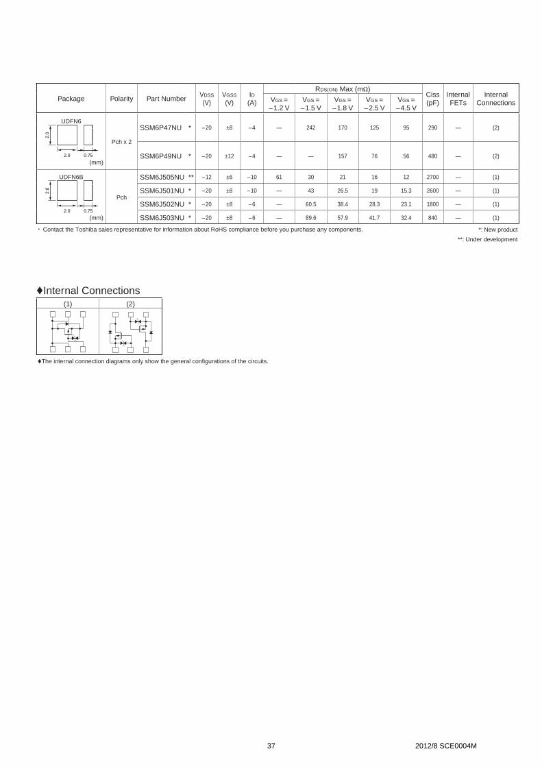
Package Polarity Part NumberVDSS
(V)VGSS
(V)ID(A)
RDS(ON) Max (mΩ)Ciss(pF)
Internal FETs
Internal ConnectionsVGS =
–1.2 VVGS = –1.5 V
VGS = –1.8 V
VGS = –2.5 V
VGS = –4.5 V
UDFN6
Pch x 2
SSM6P47NU * –20 ±8 –4 — 242 170 125 95 290 — (2)
2.0 0.75
2.0
SSM6P49NU * –20 ±12 –4 — — 157 76 56 480 — (2)(mm)
UDFN6B
Pch
SSM6J505NU ** –12 ±6 –10 61 30 21 16 12 2700 — (1)
2.0 0.75
2.0 SSM6J501NU * –20 ±8 –10 — 43 26.5 19 15.3 2600 — (1)
SSM6J502NU * –20 ±8 –6 — 60.5 38.4 28.3 23.1 1800 — (1)
(mm) SSM6J503NU * –20 ±8 –6 — 89.6 57.9 41.7 32.4 840 — (1)
x Contact the Toshiba sales representative for information about RoHS compliance before you purchase any components. *: New product
**: Under development
Internal Connections(1) (2)
The internal connection diagrams only show the general configurations of the circuits.
37 2012/8 SCE0004M

Low Voltage Power MOSFETs (|VDSS| ≤ 60 V)(Pch MOSFET) (Continued)
Package Polarity Part Number VDSS(V) VGSS(V) ID(A) PD(W)RDS(ON) Max (mΩ)
Ciss(pF)
Qg(nC) (typ.)
Internal ConnectionsVGS =
–1.5 VVGS = –1.8 V
VGS = –2.0 V
VGS = –2.5 V
VGS = –4 V
VGS = –4.5 V
VGS = –7 V
VGS = –10 V
TSM
Pch
SSM3J326T * –30 ±12 –5.6 1.25 — 115 — 62.5 — 45.7 — — 650 9.3 (6)
2.8
2.9 0.7
SSM3J314T –30 ±20 –3.5 0.7 — — — — 100 — — — 505 11.5 (6)
SSM3J306T –30 ±20 –2.4 0.7 — — — — 225 — — — 280 2.5 (6)
(mm) SSM3J305T –30 ±20 –1.7 0.7 — — — — 477 — — — 137 1.3 (6)
S-MINI
Pch SSM3J325F * –20 ±8 –2 1.2 311 231 — 179 — 150 — — 270 4.6 (6)
2.9
2.5
1.5
(mm)
SOT-23F
Pch
SSM3J328R * –20 ±8 –6 2 88.4 56 — 39.7 — 29.8 — — 840 12.8 (6)
2.9 0.8
2.4
SSM3J331R * –20 ±8 –4 2 150 100 — 75 — 55 — — 630 10.4 (6)
SSM3J327R * –20 ±8 –3.9 2 240 168 — 123 — 93 — — 290 4.6 (6)
SSM3J332R * –30 ±12 –6 2 — 144 — 72 — 50 — 47 560 8.2 (6)
(mm) SSM3J334R * –30 ±20 –4 2 — — — — — 105 — 71 280 5.9 (6)
Pch
TPCF8101 –12 ±8 –6 2.5 — 85 — 40 — 28 — — 1600 18 (2)
VS-8 TPCF8105 –20 ±12 –6 2.5 — 100 — 41 — 30 — — 1100 17 (2)
2.9
1.5
1.9
0.8
TPCF8108 –20 ±12 –7 2.5 — 95 — 37 — 26 — — 1320 19 (2)
TPCF8107 –30 –25/+20 –6 2.5 — — — — — 38 — 28 970 22 (2)
Pch x 2
TPCF8305 –20 ±12 –4 1.35 — 265 160 83 — 58 — — 680 9.2 (3)
(mm) TPCF8306 –30 –25/+20 –3.2 1.35 — — — — — 72 — 120 390 10 (3)
TPCF8304 –30 ±20 –3.2 1.35 — — — — — 105 — 72 600 14 (3)
VS-6
Pch
TPC6103 –12 ±8 –5.5 2.2 — 90 — 55 — 35 — — 1520 20 (1)
TPC6130 –20 ±12 –2.8 2.2 — — — 164 — 106 — — 360 5.1 (1)
0.75
2.8
2.9
1.6 TPC6113 –20 ±12 –5 2.2 — — — 85 — 55 — — 690 10 (1)
TPC6111 –20 ±8 –5.5 2.2 — 80 — 57 — 40 — — 700 10 (1)
TPC6110 –30 –25/+20 –4.5 2.2 — — — — — 77 — 56 510 14 (1)(mm) TPC6109-H –30 ±20 –5 2.2 — — — — — 83 — 59 490 12.3 (1)
Pch
TPCP8105 –20 ±12 –5.2 1.68 — 60 45 23 — 17 — — 2280 28 (4)PS-8 TPCP8102 –20 ±12 –7.2 1.68 — — 80 30 — 18 — — 2560 33 (4)
2.9
2.4
2.8
0.8
TPCP8106 –30 –25/+20 –7.2 1.68 — — — — — 44 — 33 870 19 (4)
TPCP8103-H –40 ±20 –4.8 1.68 — — — — — 54 — 40 800 19 (4)
Pch x 2
TPCP8303 –20 ±8 –3.8 1.48 144 90 — 60 — 46 — — 640 10 (3)
(mm) TPCP8306 –20 ±12 –4 1.48 — 265 160 83 — 58 — — 680 9.2 (3)
TPCP8305 –20 ±12 –6 1.48 — — — 42 — 30 — — 1500 21.5 (3)
x Contact the Toshiba sales representative for information about RoHS compliance before you purchase any components. *: New product
Internal Connections(1) (2) (3) (4) (6)
1
56
2 3
4
1
5678
2 3 4 1
5678
2 3 4 1
5678
2 3 4
Note: Some MOSFETs do not have a Zener diode between gate and source.
The internal connection diagrams only show the general configurations of the circuits.
38 2012/8 SCE0004M

Package Polarity Part Number VDSS(V) VGSS(V) ID(A) PD(W)RDS(ON) Max (mΩ)
Qg(nC)(typ.)
Internal ConnectionsVGS =
–1.8 VVGS = –2.0 V
VGS = –2.5 V
VGS = –4 V
VGS = –4.5 V
VGS = –7 V
VGS = –10 V
Pch
TPCC8136 –20 ±12 –9.4 18 60 37 22 — 16 — — 36 (1)
TSON Advance TPCC8137 –20 ±12 –13 30 52 30 16 — 10 — — 43 (1)
3.1
3.3
3.3
3.1
0.85
TPCC8138 –20 ±12 –18 39 42 21 11 — 7.5 — — 63 (1)
TPCC8131 –30 –25/+20 –10 20 — — — — 23 — 17.6 40 (1)
TPCC8102 –30 ±20 –15 26 — — — 33.2 — — 18.9 26 (1)
TPCC8103 –30 ±20 –18 27 — — — 25 — — 12 38 (1)
(mm) TPCC8104 –30 –25/+20 –20 27 — — — — 12.4 — 8.8 58 (1)
TPCC8105 –30 –25/+20 –23 30 — — — — 10.4 — 7.8 76 (1)
Pch
TPC8129 –30 –25/+20 –9 1.9 — — — — 22 — 28 39 (1)
TPC8119 –30 ±20 –10 1.9 — — — 28 — — 13 40 (1)
TPC8125 –30 –25/+20 –10 1.9 — — — — 17 — 13 64 (1)
TPC8121 –30 ±20 –10 1.9 — — — 24 — — 12 42 (1)
TPC8126 –30 –25/+20 –11 1.9 — — — — 14 — 10 56 (1)
SOP-8 TPC8123 –30 –25/+20 –11 1.9 — — — — 12.5 — 9 68 (1)
4.4
6.0
5.5 max 1.6
TPC8122 –30 ±20 –12 1.9 — — — 16.5 — — 8 62 (1)
TPC8118 –30 ±20 –13 1.9 — — — 15 — — 7 65 (1)
TPC8127 –30 –25/+20 –13 1.9 — — — — 8.9 — 6.5 92 (1)
TPC8128 –30 –25/+20 –16 1.9 — — — — 6.9 5 115 (1)
(mm) TPC8117 –30 ±20 –18 1.9 — — — 7.9 — — 3.9 130 (1)
TPC8120 –30 –25/+20 –18 1.9 — — — — 4.2 — 3.2 180 (1)
TPC8134 –40 –25/+20 –5 1.9 — — — — 66 — 52 20 (1)
TPC8132 –40 –25/+20 –7 1.9 — — — — 33 — 25 34 (1)
TPC8133 –40 –25/+20 –9 1.9 — — — — 18 — 15 64 (1)
TPC8124 –40 –25/+20 –12 1.9 — — — — 10 — 8 104 (1)
SOP Advance
Pch
TPCA8105 –12 ±8 –6 20 92 — 51 — 33 — — 18 (1)
5.0
5.0
6.0
5.30.95
TPCA8131 –30 –25/+20 –13 27 — — — — 22 — 17 40 (1)
TPCA8109 –30 –25/+20 –24 30 — — — — 13 — 9 56 (1)
TPCA8128 –30 –25/+20 –34 45 — — — — 6.7 — 4.8 115 (1)
TPCA8106 –30 ±20 –40 45 — — — 7.8 — — 3.7 130 (1)
(mm) TPCA8120 –30 –25/+20 –45 45 — — — — 4.0 — 3.0 190 (1)
PW-Mini
Pch 2SJ360 –60 — –1 1.5 — — — 1200 — — 730 6.5
4.6
4.2
2.5
1.6
(mm)
x Contact the Toshiba sales representative for information about RoHS compliance before you purchase any components.
Internal Connections(1)
1
5678
2 3 4
Note: Some MOSFETs do not have a Zener diode between gate and source.
The internal connection diagrams only show the general configurations of the circuits.
39 2012/8 SCE0004M
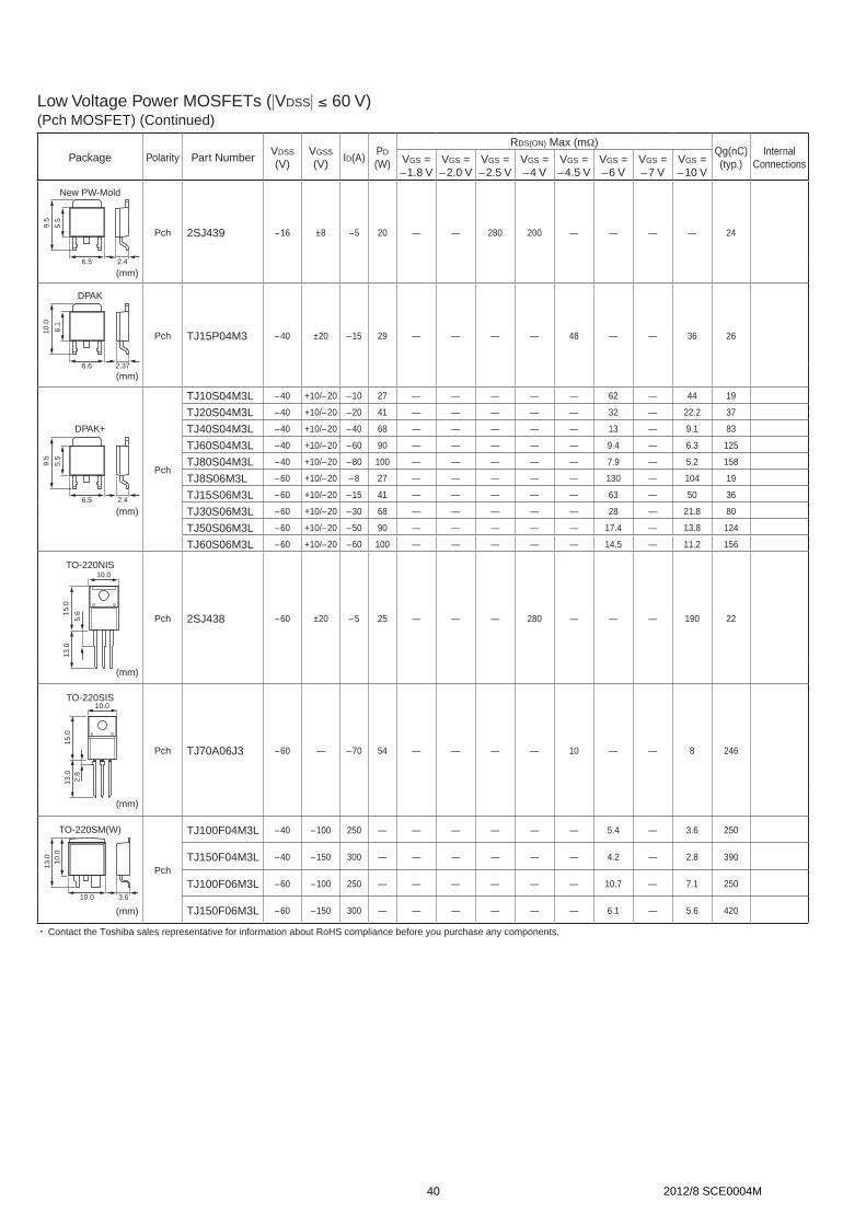
Low Voltage Power MOSFETs (|VDSS| ≤ 60 V)(Pch MOSFET) (Continued)
Package Polarity Part NumberVDSS
(V)VGSS
(V)ID(A)
PD
(W)
RDS(ON) Max (mΩ)Qg(nC)(typ.)
Internal ConnectionsVGS =
–1.8 VVGS = –2.0 V
VGS = –2.5 V
VGS = –4 V
VGS = –4.5 V
VGS = –6 V
VGS = –7 V
VGS = –10 V
New PW-Mold
Pch 2SJ439 –16 ±8 –5 20 — — 280 200 — — — — 24
9.5
2.4
5.5
6.5
(mm)
DPAK
Pch TJ15P04M3 –40 ±20 –15 29 — — — — 48 — — 36 2610.0
2.37
6.1
6.6
(mm)
Pch
TJ10S04M3L –40 +10/–20 –10 27 — — — — — 62 — 44 19
TJ20S04M3L –40 +10/–20 –20 41 — — — — — 32 — 22.2 37
DPAK+ TJ40S04M3L –40 +10/–20 –40 68 — — — — — 13 — 9.1 83
9.5
2.4
5.5
6.5
TJ60S04M3L –40 +10/–20 –60 90 — — — — — 9.4 — 6.3 125
TJ80S04M3L –40 +10/–20 –80 100 — — — — — 7.9 — 5.2 158
TJ8S06M3L –60 +10/–20 –8 27 — — — — — 130 — 104 19
TJ15S06M3L –60 +10/–20 –15 41 — — — — — 63 — 50 36
(mm) TJ30S06M3L –60 +10/–20 –30 68 — — — — — 28 — 21.8 80
TJ50S06M3L –60 +10/–20 –50 90 — — — — — 17.4 — 13.8 124
TJ60S06M3L –60 +10/–20 –60 100 — — — — — 14.5 — 11.2 156
TO-220NIS
Pch 2SJ438 –60 ±20 –5 25 — — — 280 — — — 190 22
15.0
10.0
13.0
5.6
(mm)
TO-220SIS
Pch TJ70A06J3 –60 — –70 54 — — — — 10 — — 8 246
15.0
10.0
13.0
2.8
(mm)
TO-220SM(W)
10.0
13.0
3.6
10.0
(mm)
Pch
TJ100F04M3L –40 –100 250 — — — — — — 5.4 — 3.6 250
TJ150F04M3L –40 –150 300 — — — — — — 4.2 — 2.8 390
TJ100F06M3L –60 –100 250 — — — — — — 10.7 — 7.1 250
TJ150F06M3L –60 –150 300 — — — — — — 6.1 — 5.6 420
x Contact the Toshiba sales representative for information about RoHS compliance before you purchase any components.
40 2012/8 SCE0004M

Low Voltage Power MOSFETs (|VDSS| ≤ 60 V)(Complementary MOSFETs)
Package Polarity Part NumberVDSS
(V)VGSS
(V)ID(A)
RDS(ON) Max (mΩ)Ciss(pF)
Qg(nC)(typ.)
Internal FETs
Internal Connections|VGS| =
1.5 V|VGS| = 1.8 V
|VGS| = 2.5 V
|VGS| = 4.0 V
|VGS| = 4.5 V
|VGS| = 10 V
ES6
Nch + Pch SSM6L14FE *
20 ±10 0.8 600 450 330 — 240 — 90 2.0 SSM6N42FE (1)
1.6 0.55
1.6
–20 ±8 –0.72 1040 670 440 — 300 — 110 1.76 SSM6P41FE (1)
(mm)
Nch + Pch
SSM6L39TU20 ±10 1.6 247 190 139 119 — — 265 — SSM6N39TU
+ SSM6P39TU (1)–20 ±8 –1.5 — 430 294 213 — — 250 —
UF6SSM6L12TU
30 ±12 0.5 — — 180 145 — — 245 — SSM6K24FE + SSM6J25FE (1)
2.0 0.7
2.1
–20 ±12 –0.5 — — 430 260 — — 218 —
SSM6L40TU30 ±20 1.6 — — — 182 — — 180 — SSM6N40TU
+ SSM6P40TU (1)–30 ±20 –1.4 — — — 403 — — 120 —
SSM6E03TU20 ±10 0.1 15 Ω — 4.0 Ω 3.0 Ω — — 9.3 — SSM3K16FU
(3)(mm) –20 ±8 –1.8 — 335 180 144 — — 335 — SSM3J109TU
SSM6E01TU20 ±10 0.05 — — 10 Ω — — — 11 — SSM3K04FE
(2)–12 ±12 –1 — — 240 160 — — 310 — —
VS-8
Nch + Pch TPCF8402
30 ±20 4 — — — 77 — 50 470 10 — (4)
2.9
1.5
1.9
0.8 –30 ±20 –3.2 — — — 105 — 72 600 14 — (4)(mm)
Nch + Pch
TPCP840430 ±20 4 — — — — 80 50 190 4.6 —
(4)PS-8 –30 ±20 –4 — — — — 80 50 510 13 —
2.9
2.4
2.8
0.8
TPCP840340 ±20 4.7 — — — — 60 40 770 16 —
(4)–40 ±20 –3.4 — — — — 105 70 680 15 —
TPCP840530 ±20 6.5 — — — — 29 26 830 13.8 —
(4)–30 ±20 –6 — — — — 42 31.3 1075 24.1 —
(mm)TPCP8406
40 ±20 6 — — — — 36 32 850 13.7 —(4)
–40 ±20 –5 — — — — 53.4 43.2 1105 24.2 —
SOP-8
Nch + Pch
TPC840730 ±20 9 — — — — 21 17 1190 17 —
(4)
4.4
6.0
5.5 max 1.6
–30 ±20 –7.4 — — — — 29 23 1650 39 —
TPC840840 ±20 6.1 — — — — 36 32 850 14 —
(4)(mm) –40 ±20 –5.3 — — — — 53 43 1105 24 —
x Contact the Toshiba sales representative for information about RoHS compliance before you purchase any components. *: New product
Internal Connections(1) (2) (3) (4)
Q1
Q2
Q1
Q2
Q1
Q2
1
5678
2 3 4
Note: Some MOSFETs do not have a Zener diode between gate and source.
The internal connection diagrams only show the general configurations of the circuits.
41 2012/8 SCE0004M

Low Voltage Power MOSFETs (|VDSS| ≤ 60 V)(Load SW)
Package Polarity Part NumberVDSS
(V)VGSS
(V)ID(A)
PD
(W)
RDS(ON) Max (mΩ)Ciss(pF)
Qg(nC)(typ.)
Internal Connections|VGS| =
1.5 V|VGS| = 1.8 V
|VGS| = 2.0 V
|VGS| = 2.5 V
|VGS| = 4 V
|VGS| = 4.5 V
|VGS| = 7 V
|VGS| = 10 V
PS-8
Load SW TPCP8401 –12 ±8 –5.5 1.96 — 103 — 58 — 38 — — 1520 20 (1)
2.9
2.4
2.8
0.8
(mm)
x Contact the Toshiba sales representative for information about RoHS compliance before you purchase any components.
(MOSFET + BipTr)
Package Polarity Part NumberVDSS
(V)VGSS
(V)ID(A)
PD
(W)
RDS(ON) Max (mΩ)Ciss(pF)
Qg(nC)(typ.)
Internal ConnectionsVGS =
–1.5 VVGS = –1.8V
VGS = –2.0 V
VGS = –2.5 V
VGS = –4 V
VGS = –4.5 V
VGS = –7 V
VGS = –10 V
PS-8
Pch + BipTr TPCP8J01 –32 ±20 –5.5 2.14 — — — — 49 — — 35 1760 34 (2)
2.9
2.4
2.8
0.8
(mm)
x Contact the Toshiba sales representative for information about RoHS compliance before you purchase any components.
Internal Connections(1) (2)
1
5678
2 3 4 1
5678
2 3 4
R1
R2
Note: Some MOSFETs do not have a Zener diode between gate and source.
The internal connection diagrams only show the general configurations of the circuits.
42 2012/8 SCE0004M

Low Voltage Power MOSFETs (|VDSS| ≤ 60 V)(MOSFET + SBD)
Package Polarity Part Number
MOSFET SBD
Qg(nC) (typ.)
Internal ConnectionsVDSS
(V)VGSS
(V)ID(A)
PD
(W)
RDS(ON) Max (mΩ)Ciss(pF)
VR
(V)IO(A)
VF Max (V)
|VGS| = 1.8 V
|VGS| = 2.0 V
|VGS| = 2.5 V
|VGS| = 4.0 V
|VGS| = 4.5 V
|VGS| = 10 V
IF = 1.0 A
IF = 0.5 A
IF = 0.3 A
IF = 0.1 A
UFV
Pch + SBD
SSM5G10TU –20 ±8 –1.5 — 430 — 294 213 — — 250 20 0.7 — 0.39 — — — (1)
2.0 0.7
2.1 SSM5G09TU –12 ±8 –1.5 — — — 200 130 — — 550 12 0.5 — 0.43 0.39 — — (1)
SSM5G02TU –12 ±12 –1 — — — 240 160 — — 310 12 0.5 — 0.43 0.39 — — (1)
(mm) SSM5G11TU –30 ±20 –1.4 — — — — 403 — 226 120 30 0.7 — 0.41 — — — (1)
UDFN6
SSM6G18NU * –20 ±8 –2 2 185 — 143 — 112 — 270 30 1 0.58 0.45 — — 4.6 (4)
2.0 0.75
2.0
(mm)
VS-8
TPCF8B01 –20 ±8 –2.7 1.35 300 — 160 — 110 — — 20 1 0.49 — — — 6 (3)
2.9
1.5
1.9
0.8
(mm)
UFV
Nch + SBD
SSM5H10TU 20 ±10 1.6 — 190 — 139 119 — — 260 20 0.7 — 0.39 — — — (2)
2.0 0.7
2.1
SSM5H08TU 20 ±12 1.5 — — — 220 160 — — 125 20 0.5 — — 0.45 — — (2)
SSM5H11TU 30 ±20 1.6 — — — — 182 — 122 180 30 0.7 — 0.41 — — — (2)
SSM5H16TU 30 ±12 1.9 — 296 — 177 133 — — 123 30 0.8 — 0.45 — 0.36 — (2)
SSM5H01TU 30 ±20 1.4 — — — — 450 — 200 106 20 0.5 — — 0.45 — — (2)
(mm) SSM5H07TU 20 ±20 1.2 — — — — 540 — 300 36 12 0.5 — 0.43 0.39 — — (2)
SMV
SSM5H14F 30 ±12 3 — 138 — 94 78 — — 270 45 0.1 — — — 0.6 — (2)
2.9
2.8
1.6
(mm)
x Contact the Toshiba sales representative for information about RoHS compliance before you purchase any components. *: New product
Internal Connections(1) (2) (3) (4)
1
5678
2 3 4
Note: Some MOSFETs do not have a Zener diode between gate and source.
The internal connection diagrams only show the general configurations of the circuits.
43 2012/8 SCE0004M

Low Voltage Power MOSFETs (|VDSS| ≤ 60 V)(MOSFET + SBD) (Continued)
Package Polarity Part Number
MOSFET SBD
Qg(nC) (typ.)
Internal ConnectionsVDSS
(V)VGSS
(V)ID(A)
PD
(W)
RDS(ON) Max (mΩ)Ciss(pF)
VR
(V)IO(A)
VF Max (V)
|VGS| = 1.8 V
|VGS| = 2.0 V
|VGS| = 2.5 V
|VGS| = 4.0 V
|VGS| = 4.5 V
|VGS| = 10 V
IF = 1.0 A
IF = 0.5 A
IF = 0.3 A
IF = 0.1 A
PS-8
Nch + SBD
TPCP8AA1 20 ±12 1.6 — — — 140 105 — — 306 25 0.7 — 0.41 — — — (2)
2.9
2.4
2.8
0.8 TPCP8A05-H F 30 ±20 8 1.68 — — — — 21.9 17.5 1300 — — — — — — 16 (1)(mm)
SOP-8 TPC8A05-H F 30 ±20 10 1.9 — — — — 17.6 13.3 — — — — — — — 15 (1)
4.4
6.0
5.5 max 1.6
TPC8A06-H F 30 ±20 12 1.9 — — — — 12.9 10.1 1400 — — — — — — 19 (1)
TPC8A03-H F 30 ±20 17 1.9 — — — — 7 5.6 — — — — — — — 36 (1)
(mm) TPC8A04-H F 30 ±20 18 1.9 — — — — 4.5 3.6 — — — — — — — 56 (1)
SOP Advance TPCA8A05-H F 30 ±20 20 30 — — — — 17.2 12.9 — — — — — — — 15 (1)
5.0
5.0
6.0
5.30.95
TPCA8A02-H F 30 ±20 34 45 — — — — 6.7 5.3 — — — — — — — 36 (1)
TPCA8A11-H F 30 ±20 35 52 — — — — 4.6 3.6 3200 — — — — — — 46 (1)
TPCA8A10-H F 30 ±20 40 58 — — — — 3.8 3 4000 — — — — — — 57 (1)
(mm) TPCA8A09-H F 30 ±20 51 70 — — — — 2.8 2.3 5900 — — — — — — 82 (1)
F: Monolithic
x Contact the Toshiba sales representative for information about RoHS compliance before you purchase any components.
Internal Connections(1) (2)
1
5678
2 3 4
The internal connection diagrams only show the general configurations of the circuits.
44 2012/8 SCE0004M
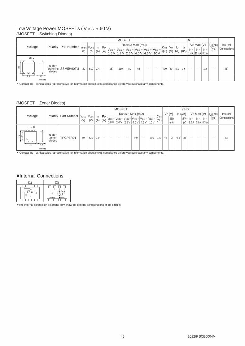
Low Voltage Power MOSFETs (|VDSS| ≤ 60 V)(MOSFET + Switching Diodes)
Package Polarity Part Number
MOSFET Di
Qg(nC) (typ.)
Internal ConnectionsVDSS
(V)VGSS
(V)ID(A)
PD
(W)
RDS(ON) Max (mΩ)Ciss(pF)
VR
(V)IO(A)
trr (ns)
VF Max (V)
VGS = 1.5 V
VGS = 1.8 V
VGS = 2.5 V
VGS = 4.0 V
VGS = 4.5 V
VGS = 10 V
IF = 1 mA
IF = 10 mA
IF = 0.1 A
UFV
N-ch + Switching
diodesSSM5H90TU 20 ±10 2.4 — 157 110 80 65 — — 400 80 0.1 1.6 — — 1.2 — (1)
2.0 0.7
2.1
(mm)
x Contact the Toshiba sales representative for information about RoHS compliance before you purchase any components.
(MOSFET + Zener Diodes)
Package Polarity Part Number
MOSFET Ze-Di
Qg(nC) (typ.)
Internal ConnectionsVDSS
(V)VGSS
(V)ID(A)
PD
(W)
RDS(ON) Max (mΩ)Ciss(pF)
VZ (V) IR (mA) VF Max (V)
VGS = 1.8 V
VGS = 2.0 V
VGS = 2.5 V
VGS = 4.0 V
VGS = 4.5 V
VGS = 10 V
@IZ (mA)
@VR (V)
IF = 1.0 A
IF = 0.5 A
IF = 0.3 A
PS-8
N-ch + Zener diodes
TPCP8R01 60 ±20 2.0 — — — — 440 — 300 140 43 2 0.5 33 — — — — (2)
2.9
2.4
2.8
0.8
(mm)
x Contact the Toshiba sales representative for information about RoHS compliance before you purchase any components.
Internal Connections(1) (2)
The internal connection diagrams only show the general configurations of the circuits.
45 2012/8 SCE0004M

Low Voltage Power MOSFETs (60 V < |VDSS| ≤ 300 V)(Nch MOSFET)
Package Polarity Part Number VDSS(V) VGSS(V) ID(A) PD(W)RDS(ON) Max (mΩ)
Qg(nC)(typ.)
Internal ConnectionsVGS =
1.8 VVGS = 2.0 V
VGS = 2.5 V
VGS = 4 V
VGS = 4.5 V
VGS = 7 V
VGS = 10 V
PS-8
Nch TPCP8003-H 100 ±20 2.2 1.68 — — — — 190 — 180 7.5 (1)
2.9
2.4
2.8
0.8
(mm)
SOP-8
Nch
TPC8051-H 80 ±20 13 1.9 — — — — 10.1 — 9.7 85 (1)
4.4
6.0
5.5 max 1.6 TPC8012-H 200 ±20 1.8 1.9 — — — — — — 400 11 (1)
(mm)
SOP Advance
Nch
TPCA8051-H 80 ±20 28 45 — — — — 9.8 — 9.4 91 (1)
5.0
5.0
6.0
5.30.95
TPCA8006-H 100 ±20 18 45 — — — — — — 67 12 (1)
TPCA8010-H 200 ±20 5.5 45 — — — — — — 450 10 (1)
(mm) TPCA8008-H 250 ±20 4 45 — — — — — — 580 10 (1)
PW-Mini
Nch
2SK2963 100 — 1 1.5 — — — 950 — — 700 6.3
4.6
4.2
2.5
1.6 2SK2992 200 — 1 1.5 — — — — — — 3500 3(mm)
x Contact the Toshiba sales representative for information about RoHS compliance before you purchase any components.
Internal Connections(1)
1
5678
2 3 4
Note: Some MOSFETs do not have a Zener diode between gate and source.
The internal connection diagrams only show the general configurations of the circuits.
46 2012/8 SCE0004M

Package Polarity Part Number VDSS(V) ID(A) PD(W)RDS(ON) Max (mΩ)
Qg(nC)(typ.)
Internal ConnectionsVGS =
1.8 VVGS = 2.0 V
VGS = 2.5 V
VGS = 4 V
VGS = 4.5 V
VGS = 6 V
VGS = 10 V
New PW-Mold
Nch
2SK2201 100 3 20 — — — 450 — — 350 13.5
2SK2399 100 5 20 — — — 300 — — 230 22
9.5
2.4
5.5
6.5
2SK3669 100 10 20 — — — — — — 125 8.0
2SK3205 150 5 20 — — — 750 — — 500 12
2SK2920 200 5 20 — — — — — — 800 10
2SK3462 250 3 20 — — — — — — 1700 12(mm)
2SK3342 250 4.5 20 — — — — — — 1000 10
New PW-Mold2
Nch
2SK4018 100 3 20 — — — 450 — — 350 13.5
5.5
5.7
6.5
7.0
1.6
2SK4019 100 5 20 — — — 300 — — 230 22
2SK4020 200 5 20 — — — — — — 800 10
2SK4022 250 3 20 — — — — — — 1700 12
(mm) 2SK4021 250 4.5 20 — — — — — — 1000 10
DPAK
Nch
TK8P25DA 250 7.5 55 — — — — — — 500 16
10.0
2.37
6.1
6.6 TK13P25D 250 13 96 — — — — — — 250 25
(mm)
DPAK+
Nch TK40S10K3Z 100 40 93 — — — — — — 18 61
9.5
2.4
5.5
6.5
(mm)
TO-220SM
10.35
10.4
5
15.3
4.46
(mm)
Nch
TK100G08N1 ** 80 (224) 250 — — — — — — (2.8) —
TK65G10N1 ** 100 (151) 192 — — — — — — (4.5) 81
TK100G10N1 ** 100 (212) 250 — — — — — — (3.1) —
TK100G12N1 ** 120 (181) 250 — — — — — — (4.1) —
TO-220SM(W)
10.0
13.0
3.6
10.0
(mm)
Nch
TK55F08K3L 75 55 125 — — — — — 12 10.2 67
TK60F08K3 75 60 150 — — — — — — 8.5 75
TK80F08K3 75 80 300 — — — — — — 4.3 175
x Contact the Toshiba sales representative for information about RoHS compliance before you purchase any components. **: Under development
47 2012/8 SCE0004M
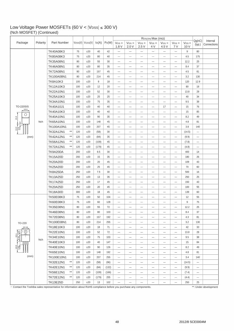
Low Voltage Power MOSFETs (60 V < |VDSS| ≤ 300 V)(Nch MOSFET) (Continued)
Package Polarity Part Number VDSS(V) VGSS(V) ID(A) PD(W)RDS(ON) Max (mΩ)
Qg(nC)(typ.)
Internal ConnectionsVGS =
1.8 VVGS = 2.0 V
VGS = 2.5 V
VGS = 4 V
VGS = 4.5 V
VGS = 7 V
VGS = 10 V
TO-220SIS
15.0
10.0
13.0
2.8
(mm)
Nch
TK40A08K3 75 ±20 40 42 — — — — — — 9 80
TK80A08K3 75 ±20 80 40 — — — — — — 4.5 175
TK35A08N1 80 ±20 55 30 — — — — — — 12.2 25
TK46A08N1 80 ±20 80 35 — — — — — — 8.4 37
TK72A08N1 80 ±20 157 45 — — — — — — 4.5 81
TK100A08N1 80 ±20 214 45 — — — — — — 3.2 130
TK8A10K3 100 ±20 8 18 — — — — — — 120 12.9
TK12A10K3 100 ±20 12 20 — — — — — — 80 18
TK22A10N1 100 ±20 52 30 — — — — — — 13.8 28
TK25A10K3 100 ±20 25 25 — — — — — — 40 34
TK34A10N1 100 ±20 75 35 — — — — — — 9.5 38
TK40A10J1 100 ±20 40 40 — — — — 17 — 15 76
TK40A10K3 100 ±20 40 40 — — — — — — 15 85
TK40A10N1 100 ±20 90 35 — — — — — — 8.2 49
TK65A10N1 100 ±20 148 45 — — — — — — 4.8 81
TK100A10N1 100 ±20 207 45 — — — — — — 3.8 140
TK32A12N1 ** 120 ±20 (58) 30 — — — — — — (14.5) —
TK42A12N1 ** 120 ±20 (84) 35 — — — — — — (9.9) —
TK56A12N1 ** 120 ±20 (109) 45 — — — — — — (7.8) —
TK72A12N1 ** 120 ±20 (179) 45 — — — — — — (4.8) —
TK9A20DA 200 ±20 8.5 30 — — — — — — 400 14
TK15A20D 200 ±20 15 35 — — — — — — 180 26
TK20A20D 200 ±20 20 45 — — — — — — 109 43
TK25A20D 200 ±20 25 45 — — — — — — 70 60
TK8A25DA 250 ±20 7.5 30 — — — — — — 500 16
TK13A25D 250 ±20 13 35 — — — — — — 250 25
TK17A25D 250 ±20 17 45 — — — — — — 150 43
TK20A25D 250 ±20 20 45 — — — — — — 100 55
TK18A30D 300 ±20 18 45 — — — — — — 139 60
TO-220
15.1
3.85
8.59
13.9
6.51
10.16
(mm)
Nch
TK50E08K3 75 ±20 50 104 — — — — — — 12 55
TK60E08K3 75 ±20 60 128 — — — — — — 9 75
TK35E08N1 80 ±20 55 72 — — — — — — 12.2 25
TK46E08N1 80 ±20 80 103 — — — — — — 8.4 37
TK72E08N1 80 ±20 157 192 — — — — — — 4.3 81
TK100E08N1 80 ±20 214 255 — — — — — — 3.2 130
TK18E10K3 100 ±20 18 71 — — — — — — 42 33
TK22E10N1 100 ±20 52 72 — — — — — — 13.8 28
TK34E10N1 100 ±20 75 103 — — — — — — 9.5 38
TK40E10K3 100 ±20 40 147 — — — — — — 15 84
TK40E10N1 100 ±20 90 126 — — — — — — 8.2 49
TK65E10N1 100 ±20 148 192 — — — — — — 4.8 81
TK100E10N1 100 ±20 207 255 — — — — — — 3.4 140
TK32E12N1 ** 120 ±20 (58) (96) — — — — — — (14.5) —
TK42E12N1 ** 120 ±20 (84) (132) — — — — — — (9.9) —
TK56E12N1 ** 120 ±20 (109) (166) — — — — — — (7.4) —
TK72E12N1 ** 120 ±20 (179) 255 — — — — — — (4.4) —
TK13E25D 250 ±20 13 102 — — — — — — 250 25
x Contact the Toshiba sales representative for information about RoHS compliance before you purchase any components. **: Under development
48 2012/8 SCE0004M

Package Polarity Part Number VDSS(V) VGSS(V) ID(A) PD(W)RDS(ON) Max (mΩ)
Qg(nC)(typ.)
Internal ConnectionsVGS =
1.8 VVGS = 2.0 V
VGS = 2.5 V
VGS = 4 V
VGS = 4.5 V
VGS = 7 V
VGS = 10 V
TO-3P(N)
Nch
2SK3940 75 — 70 150 — — — — — — 7 20015.9
20.5
20.0
3.3
TK40J20D 200 ±20 40 260 — — — — — — 44 100
TK70J20D 200 ±20 70 410 — — — — — — 27 160
TK30J25D 250 ±20 30 260 — — — — — — 60 100
TK60J25D 250 ±20 60 410 — — — — — — 38 160
(mm) TK50J30D 300 ±20 50 410 — — — — — — 52 160
TO-3P(N)IS
Nch 2SK2995 250 — 30 90 — — — — — — 68 132
15.8
21.0
19.4 3.6
(mm)
x Contact the Toshiba sales representative for information about RoHS compliance before you purchase any components.
49 2012/8 SCE0004M

Low Voltage Power MOSFETs (60 V < |VDSS| ≤ 300 V)(Pch MOSFET)
Package Polarity Part Number VDSS(V) VGSS(V) ID(A) PD(W)RDS(ON) Max (mΩ)
Qg(nC)(typ.)
Internal ConnectionsVGS =
–1.8 VVGS = –2.0 V
VGS = –2.5 V
VGS = –4 V
VGS = –4.5 V
VGS = –7 V
VGS = –10 V
New PW-Mold
Pch
2SJ567 –200 — –2.5 20 — — — — — — 2000 10
9.5
2.4
5.5
6.5 2SJ610 –250 — –2 20 — — — — — — 2550 24
(mm)
New PW-Mold2
Pch 2SJ680 –200 — –2.5 20 — — — — — — 2000 105.5
5.7
6.5
7.0
1.6
(mm)
TO-220SIS
Pch
TJ9A10M3 –100 ±20 –9 19 — — — — — — 170 47
15.0
10.0
13.0
2.8
TJ11A10M3 –100 ±20 –11 24 — — — — — — 130 69
TJ20A10M3 –100 ±20 –20 35 — — — — — — 90 120(mm)
x Contact the Toshiba sales representative for information about RoHS compliance before you purchase any components.
50 2012/8 SCE0004M

Middle-high Voltage Power MOSFETs (300 V < |VDSS| ≤ 700 V)(Nch MOSFET)
Package Polarity Part Number VDSS(V) ID(A) PD(W)RDS(ON) Max (Ω) Qg(nC)
(typ.)Internal
ConnectionsVGS = 10 V
PW-Mini
Nch 2SK3471 500 0.5 1.5 18 3.8
4.6
4.2
2.5
1.6
(mm)
New PW-Mold
Nch TK2P60D 600 2 60 4.3 7
9.5
2.4
5.5
6.5
(mm)
New PW-Mold2
5.5
5.7
6.5
7.0
1.6
(mm)
Nch
2SK4023 450 1 20 4.6 5
2SK4026 600 1 20 9.0 9
TK2Q60D 600 2 60 4.3 7
2SK4003 600 3 20 2.2 15
TK4Q60DA 600 3.5 80 2.2 11
Nch
TK3P50D 500 3 60 3.0 7
TK4P50D 500 4 80 2.0 9
TK5P50D 500 5 80 1.5 11
TK7P50D 500 7 100 1.22 12DPAK
10.0
2.37
6.1
6.6
TK5P53D 525 5 80 1.5 11
TK6P53D 525 6 100 1.3 12
(mm) TK4P55DA 550 3.5 80 2.45 9
TK4P55D 550 4 80 1.88 11
TK4P60DA 600 3.5 80 1.7 11
TK4P60DB 600 3.7 80 2.0 11
x Contact the Toshiba sales representative for information about RoHS compliance before you purchase any components.
51 2012/8 SCE0004M

Middle-high Voltage Power MOSFETs (300 V < |VDSS| ≤ 700 V)(Nch MOSFET) (Continued)
Package Polarity Part Number VDSS(V) ID(A) PD(W)RDS(ON) Max (Ω) Qg(nC)
(typ.)Internal
ConnectionsVGS = 10 V
TO-220
Nch
TK12E60U 600 12 144 0.4 14
15.1
3.85
8.59
13.9
6.51
10.16
TK15E60U 600 15 170 0.3 17
TK20E60U 600 20 190 0.19 27(mm)
Nch
TK5A45DA 450 4.5 30 1.75 9
TK6A45DA 450 5.5 35 1.35 11
TK7A45DA 450 6.5 35 1.2 11
TK8A45DA 450 7.5 35 1.1 12
TK8A45D 450 8 35 0.9 16
TK9A45D 450 9 40 0.77 16
TK11A45D 450 11 40 0.62 20
TK12A45D 450 12 45 0.52 24
TK13A45D 450 13 45 0.46 25
TK14A45DA 450 13.5 45 0.41 28
TK14A45D 450 14 45 0.34 38
TK16A45D 450 16 50 0.27 40
TK19A45D 450 19 50 0.25 45
TK4A50D 500 4 30 2.0 9
TK5A50D 500 5 35 1.5 11
TK6A50D 500 6 35 1.4 11
TK7A50D 500 7 35 1.22 12
TK8A50DA 500 7.5 35 1.04 16
TK8A50D 500 8 40 0.85 16
TO-220SIS TK10A50D 500 10 45 0.72 20
TK11A50D 500 11 45 0.6 38
15.0
10.0
13.0
2.8
TK12A50D 500 12 45 0.52 25
TK13A50DA 500 12.5 45 0.47 28
TK13A50D 500 13 45 0.4 32
TK15A50D 500 15 50 0.3 40
TK18A50D 500 18 50 0.27 45
TK4A53D 525 4 35 1.7 11(mm) TK5A53D 525 5 35 1.5 11
TK6A53D 525 6 35 1.3 12
TK12A53D 525 12 45 0.58 25
TK4A55DA 550 3.5 30 2.45 9
TK4A55D 550 4 35 1.88 11
TK5A55D 550 5 35 1.7 11
TK6A55DA 550 5.5 35 1.48 12
TK7A55D 550 7 35 1.25 16
TK8A55DA 550 7.5 40 1.07 16
TK9A55DA 550 8.5 40 0.86 20
TK10A55D 550 10 45 0.72 24
TK11A55D 550 11 45 0.63 25
TK12A55D 550 12 45 0.57 28
TK13A55DA 550 12.5 45 0.48 38
TK14A55D 550 14 50 0.37 40
TK16A55D 550 16 50 0.33 45
TK3A60DA 600 2.5 30 2.8 9
TK4A60DA 600 3.5 35 2.2 11
TK4A60DB 600 3.7 35 2 11
x Contact the Toshiba sales representative for information about RoHS compliance before you purchase any components.
52 2012/8 SCE0004M

Package Polarity Part Number VDSS(V) ID(A) PD(W)RDS(ON) Max (Ω) Qg(nC)
(typ.)Internal
ConnectionsVGS = 10 V
Nch
TK4A60D 600 4 35 1.7 12
TK5A60D 600 5 35 1.43 16
TK6A60D 600 6 40 1.25 16
TK6A60W ** 600 6.2 30 0.75 12
TK8A60DA 600 7.5 45 1.0 20
TK9A60D 600 9 45 0.83 24
TK10A60D 600 10 45 0.75 25
TK10A60W ** 600 9.7 30 0.38 20
TK11A60D 600 11 45 0.65 28
TK12A60D 600 12 45 0.55 38
TK12A60U 600 12 35 0.4 14
TK12A60W ** 600 11.5 35 0.3 25
TO-220SISTK13A60D 600 13 40 0.43 40
TK15A60D 600 15 50 0.37 45
15.0
10.0
13.0
2.8
TK15A60U 600 15 40 0.3 17
TK16A60W ** 600 15.8 40 0.19 38
TK18A60V 600 18 40 0.19 39
TK20A60U 600 20 45 0.19 27
TK2A65D 650 2 30 3.26 9
TK3A65DA 650 2.5 35 2.51 11(mm)
TK3A65D 650 3 35 2.25 11
TK4A65DA 650 3.5 35 1.9 12
TK5A65DA 650 4.5 35 1.67 16
TK5A65D 650 5 40 1.43 16
TK6A65D 650 6 45 1.11 20
TK7A65D 650 7 45 0.98 24
TK8A65D 650 8 45 0.84 25
TK11A65D 650 11 45 0.7 38
TK12A65D 650 12 50 0.54 40
TK13A65D 650 13 50 0.47 45
TK13A65U 650 13 40 0.38 17
TK17A65U 650 17 45 0.26 27
TK31A60W ** 600 30.8 45 0.088 87
Nch
TK15J50D 500 15 210 0.4 32
TK20J50D 500 20 280 0.27 45
TK12J55D 550 12 190 0.57 28
TO-3P(N)TK16J55D 550 16 250 0.37 40
TK19J55D 550 19 280 0.33 4515.9
20.5
20.0
3.3
TK12J60U 600 12 144 0.4 14
TK15J60U 600 15 170 0.3 17
TK20J60U 600 20 190 0.19 27
TK40J60U 600 40 320 0.08 55
TK50J60U 600 50 400 0.065 67
TK13J65U 650 13 170 0.38 17(mm)
TK17J65U 650 17 190 0.26 27
TK31J60W ** 600 30.8 230 0.088 87
TK39J60W ** 600 38.8 270 0.065 110
TK62J60W ** 600 61.8 400 0.04 178
TO-3P(N)IS
Nch
2SK2917 500 18 90 0.27 8015.8
21.0
19.4 3.6
TK40M60U 600 40 90 0.08 55
(mm)
x Contact the Toshiba sales representative for information about RoHS compliance before you purchase any components. **: Under development
53 2012/8 SCE0004M

High Voltage Power MOSFETs (700 V < |VDSS|)(Nch MOSFET)
Package Polarity Part Number VDSS(V) ID(A) PD(W)RDS(ON) Max (Ω) Qg(nC)
(typ.)Internal
ConnectionsVGS = 10 VNew PW-Mold
Nch TK1P90A 900 1 20 9.0 13
9.5
2.4
5.5
6.5
(mm)
New PW-Mold2
Nch TK1Q90A 900 1 20 9.0 135.5
5.7
6.5
7.0
1.6
(mm)
TO-220SIS
Nch
2SK4013 800 6 45 1.7 45
15.0
10.0
13.0
2.8
2SK3566 900 2.5 40 6.4 12
2SK3564 900 3 40 4.3 17
2SK3798 900 4 40 3.5 26
2SK3565 900 5 45 2.5 28
2SK3742 900 5 45 2.5 25
2SK4014 900 6 45 2.0 45
(mm) 2SK3799 900 8 50 1.3 62
TO-3P(N)
Nch
2SK3633 800 7 150 1.7 35
15.9
20.5
20.0
3.3
2SK2719 900 3 125 4.3 25
2SK3700 900 5 150 2.5 28
2SK4115 900 7 150 2.0 45
2SK3473 900 9 150 1.6 38
2SK3878 900 9 150 1.3 62
2SK2968 900 10 150 1.25 70
(mm) 2SK4207 900 13 150 0.95 45
TO-3P(N)IS
Nch
2SK3880 800 6.5 80 1.7 3515.8
21.0
19.4 3.6
2SK2847 900 8 85 1.4 58
2SK3017 900 8.5 90 1.25 70(mm)
x Contact the Toshiba sales representative for information about RoHS compliance before you purchase any components.
54 2012/8 SCE0004M
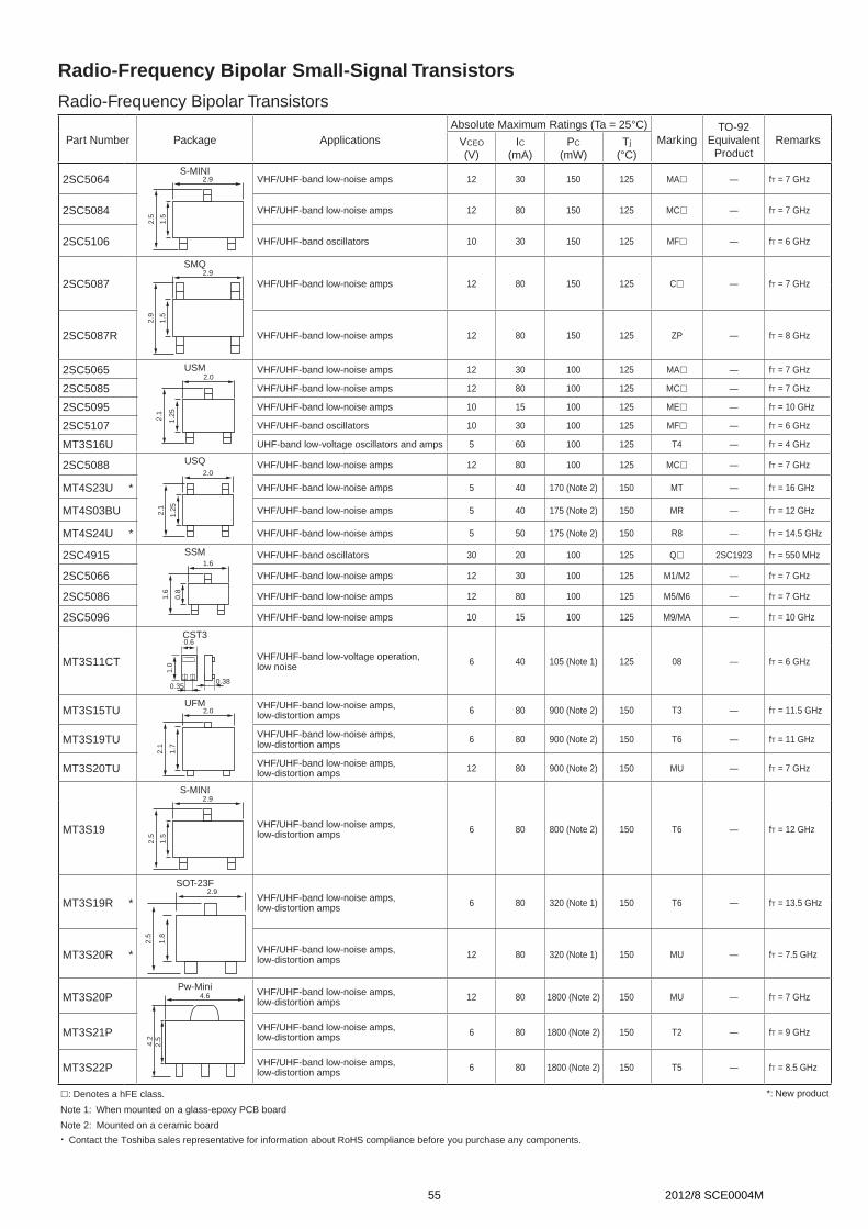
Radio-Frequency Bipolar Small-Signal Transistors
Radio-Frequency Bipolar Transistors
Part Number Package ApplicationsAbsolute Maximum Ratings (Ta = 25°C)
MarkingTO-92
EquivalentProduct
RemarksVCEO
(V)IC
(mA)PC
(mW)Tj
(°C)
2SC5064S-MINI
VHF/UHF-band low-noise amps 12 30 150 125 MA — fT = 7 GHz
2SC5084
2.9
2.5
1.5
VHF/UHF-band low-noise amps 12 80 150 125 MC — fT = 7 GHz
2SC5106 VHF/UHF-band oscillators 10 30 150 125 MF — fT = 6 GHz
2SC5087
SMQ
VHF/UHF-band low-noise amps 12 80 150 125 C — fT = 7 GHz2.9
2.9
1.5
2SC5087R VHF/UHF-band low-noise amps 12 80 150 125 ZP — fT = 8 GHz
2SC5065 USM VHF/UHF-band low-noise amps 12 30 100 125 MA — fT = 7 GHz
2SC50852.0
2.1
1.25
VHF/UHF-band low-noise amps 12 80 100 125 MC — fT = 7 GHz
2SC5095 VHF/UHF-band low-noise amps 10 15 100 125 ME — fT = 10 GHz
2SC5107 VHF/UHF-band oscillators 10 30 100 125 MF — fT = 6 GHz
MT3S16U UHF-band low-voltage oscillators and amps 5 60 100 125 T4 — fT = 4 GHz
2SC5088 USQ VHF/UHF-band low-noise amps 12 80 100 125 MC — fT = 7 GHz
MT4S23U *
2.0
2.1
1.25
VHF/UHF-band low-noise amps 5 40 170 (Note 2) 150 MT — fT = 16 GHz
MT4S03BU VHF/UHF-band low-noise amps 5 40 175 (Note 2) 150 MR — fT = 12 GHz
MT4S24U * VHF/UHF-band low-noise amps 5 50 175 (Note 2) 150 R8 — fT = 14.5 GHz
2SC4915 SSM VHF/UHF-band oscillators 30 20 100 125 Q 2SC1923 fT = 550 MHz
2SC50661.6
1.6
0.8
VHF/UHF-band low-noise amps 12 30 100 125 M1/M2 — fT = 7 GHz
2SC5086 VHF/UHF-band low-noise amps 12 80 100 125 M5/M6 — fT = 7 GHz
2SC5096 VHF/UHF-band low-noise amps 10 15 100 125 M9/MA — fT = 10 GHz
MT3S11CT
CST3
VHF/UHF-band low-voltage operation, low noise 6 40 105 (Note 1) 125 08 — fT = 6 GHz
0.6
0.350.38
1.0
MT3S15TUUFM VHF/UHF-band low-noise amps,
low-distortion amps 6 80 900 (Note 2) 150 T3 — fT = 11.5 GHz
MT3S19TU
2.0
2.1
1.7
VHF/UHF-band low-noise amps, low-distortion amps 6 80 900 (Note 2) 150 T6 — fT = 11 GHz
MT3S20TU VHF/UHF-band low-noise amps, low-distortion amps 12 80 900 (Note 2) 150 MU — fT = 7 GHz
MT3S19
S-MINI
VHF/UHF-band low-noise amps, low-distortion amps 6 80 800 (Note 2) 150 T6 — fT = 12 GHz
2.9
2.5
1.5
MT3S19R *
SOT-23F
VHF/UHF-band low-noise amps, low-distortion amps 6 80 320 (Note 1) 150 T6 — fT = 13.5 GHz
2.9
2.5
1.8
MT3S20R * VHF/UHF-band low-noise amps, low-distortion amps 12 80 320 (Note 1) 150 MU — fT = 7.5 GHz
MT3S20PPw-Mini VHF/UHF-band low-noise amps,
low-distortion amps 12 80 1800 (Note 2) 150 MU — fT = 7 GHz
MT3S21P
4.6
4.2
2.5
VHF/UHF-band low-noise amps, low-distortion amps 6 80 1800 (Note 2) 150 T2 — fT = 9 GHz
MT3S22P VHF/UHF-band low-noise amps, low-distortion amps 6 80 1800 (Note 2) 150 T5 — fT = 8.5 GHz
: Denotes a hFE class. *: New product
Note 1: When mounted on a glass-epoxy PCB board
Note 2: Mounted on a ceramic board
x Contact the Toshiba sales representative for information about RoHS compliance before you purchase any components.
55 2012/8 SCE0004M
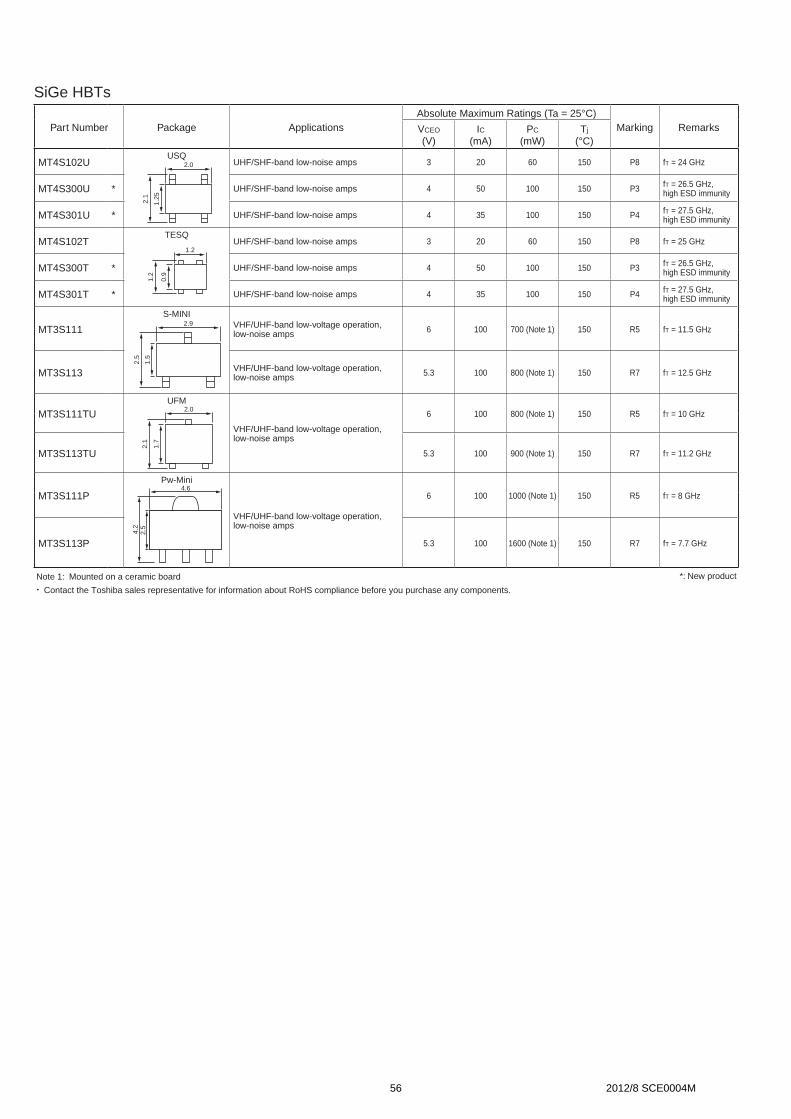
SiGe HBTs
Part Number Package ApplicationsAbsolute Maximum Ratings (Ta = 25°C)
Marking RemarksVCEO
(V)IC
(mA)PC
(mW)Tj
(°C)
MT4S102UUSQ
UHF/SHF-band low-noise amps 3 20 60 150 P8 fT = 24 GHz
MT4S300U *
2.0
2.1
1.25
UHF/SHF-band low-noise amps 4 50 100 150 P3 fT = 26.5 GHz, high ESD immunity
MT4S301U * UHF/SHF-band low-noise amps 4 35 100 150 P4 fT = 27.5 GHz, high ESD immunity
MT4S102TTESQ
UHF/SHF-band low-noise amps 3 20 60 150 P8 fT = 25 GHz
MT4S300T *
1.2
1.2
0.9
UHF/SHF-band low-noise amps 4 50 100 150 P3 fT = 26.5 GHz, high ESD immunity
MT4S301T * UHF/SHF-band low-noise amps 4 35 100 150 P4 fT = 27.5 GHz, high ESD immunity
MT3S111
S-MINIVHF/UHF-band low-voltage operation, low-noise amps 6 100 700 (Note 1) 150 R5 fT = 11.5 GHz
2.9
2.5
1.5
MT3S113 VHF/UHF-band low-voltage operation, low-noise amps 5.3 100 800 (Note 1) 150 R7 fT = 12.5 GHz
MT3S111TUUFM
VHF/UHF-band low-voltage operation, low-noise amps
6 100 800 (Note 1) 150 R5 fT = 10 GHz2.0
2.1
1.7
MT3S113TU 5.3 100 900 (Note 1) 150 R7 fT = 11.2 GHz
MT3S111P
Pw-Mini
VHF/UHF-band low-voltage operation, low-noise amps
6 100 1000 (Note 1) 150 R5 fT = 8 GHz4.6
4.2
2.5
MT3S113P 5.3 100 1600 (Note 1) 150 R7 fT = 7.7 GHz
Note 1: Mounted on a ceramic board *: New product
x Contact the Toshiba sales representative for information about RoHS compliance before you purchase any components.
56 2012/8 SCE0004M
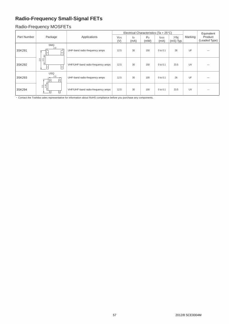
Radio-Frequency Small-Signal FETs
Radio-Frequency MOSFETs
Part Number Package ApplicationsElectrical Characteristics (Ta = 25°C)
MarkingEquivalent
Product(Leaded Type)
VDS
(V)ID
(mA)PD
(mW)IDSS
(mA)|Yfs|
(mS) Typ.
3SK291
SMQ
UHF-band radio-frequency amps 12.5 30 150 0 to 0.1 26 UF —2.9
2.9
1.5
3SK292 VHF/UHF-band radio-frequency amps 12.5 30 150 0 to 0.1 23.5 UV —
3SK293USQ
UHF-band radio-frequency amps 12.5 30 100 0 to 0.1 26 UF —2.0
2.1
1.25
3SK294 VHF/UHF-band radio-frequency amps 12.5 30 100 0 to 0.1 23.5 UV —
x Contact the Toshiba sales representative for information about RoHS compliance before you purchase any components.
57 2012/8 SCE0004M
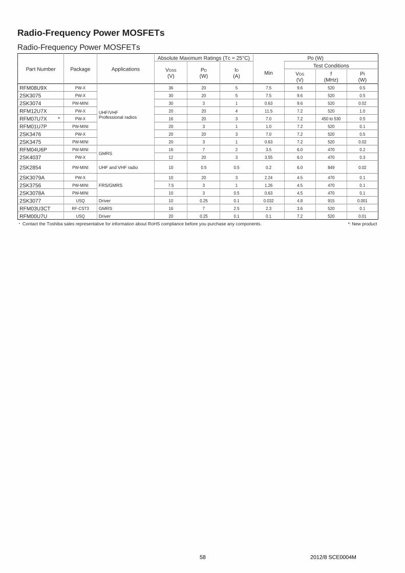
Radio-Frequency Power MOSFETs
Radio-Frequency Power MOSFETs
Part Number Package Applications
Absolute Maximum Ratings (Tc = 25°C) Po (W)
VDSS
(V)PD
(W)ID (A)
MinTest Conditions
VDS
(V)f
(MHz)Pi
(W)
RFM08U9X PW-X
UHF/VHFProfessional radios
36 20 5 7.5 9.6 520 0.5
2SK3075 PW-X 30 20 5 7.5 9.6 520 0.5
2SK3074 PW-MINI 30 3 1 0.63 9.6 520 0.02
RFM12U7X PW-X 20 20 4 11.5 7.2 520 1.0
RFM07U7X * PW-X 16 20 3 7.0 7.2 450 to 530 0.5
RFM01U7P PW-MINI 20 3 1 1.0 7.2 520 0.1
2SK3476 PW-X 20 20 3 7.0 7.2 520 0.5
2SK3475 PW-MINI 20 3 1 0.63 7.2 520 0.02
RFM04U6P PW-MINIGMRS
16 7 2 3.5 6.0 470 0.2
2SK4037 PW-X 12 20 3 3.55 6.0 470 0.3
2SK2854 PW-MINI UHF and VHF radio 10 0.5 0.5 0.2 6.0 849 0.02
2SK3079A PW-X
FRS/GMRS
10 20 3 2.24 4.5 470 0.1
2SK3756 PW-MINI 7.5 3 1 1.26 4.5 470 0.1
2SK3078A PW-MINI 10 3 0.5 0.63 4.5 470 0.1
2SK3077 USQ Driver 10 0.25 0.1 0.032 4.8 915 0.001
RFM03U3CT RF-CST3 GMRS 16 7 2.5 2.3 3.6 520 0.1
RFM00U7U USQ Driver 20 0.25 0.1 0.1 7.2 520 0.01
x Contact the Toshiba sales representative for information about RoHS compliance before you purchase any components. *: New product
58 2012/8 SCE0004M

IGBTs
IGBTs(Discrete IGBTs)
Part Number Applications Features
Absolute Maximum Ratings (Ta = 25°C)Package Circuit
Configuration(Note)
VCE(sat) Typ.@Ta = 25°C
tf Typ.@Ta = 25°C
RemarksVCES
(V)
Ic Pc
DC(A)
Pulsed(A)
Ta = 25°C (W)
Tc = 25°C (W)
Type
(V)Ic (A)
VGE (V)
(ms)
Test Conditions
GT15J341 *
Power supplies(and UPS/PFC/
Motor)
High-speedswitching
600
15 60 — 30 TO-220SIS Isolation, Through-hole (2) 1.5 15 15 0.08
Inductive load
6th generation
GT20J341 * 20 80 — 45 TO-220SIS Isolation, Through-hole (2) 1.5 20 15 0.05 6th generation
GT30J121 30 60 — 170 TO-3P(N) Through-hole (1) 2.0 30 15 0.05
GT30J126 30 60 — 90 TO-3P(N)IS Isolation, Through-hole (1) 1.95 30 15 0.05
GT30J341 * 59 120 — 230 TO-3P(N) Through-hole (2) 1.5 30 15 0.04 6th generation, Tj = 175°C
GT50J121 50 100 — 240 TO-3P(LH) Through-hole (1) 2.0 50 15 0.05
GT30J122Power factor
correction
Lowfrequency switching
30 100 — 75 TO-3P(N)IS Isolation, Through-hole (1) 2.1 50 15 0.25
Resistive load
Partial switching converter
GT30J122A 30 100 — 120 TO-3P(N) Through-hole (1) 1.7 50 15 0.2
GT40J121 40 100 — 80 TO-3P(N)IS Isolation, Through-hole (1) 1.45 40 15 0.2
GT30J322
IH rice cookers,IH cooktops,
Microwave ovens,Induction heating
equipmentAC200 V
Current resonance
30 100 — 75 TO-3P(N)IS Isolation, Through-hole (2) 2.1 50 15 0.25
GT35J321 37 100 — 75 TO-3P(N)IS Isolation, Through-hole (2) 1.9 50 15 0.19
GT40J324 * 40 100 — 200 TO-3P(N) Through-hole (2) 2.1 40 15 0.04 6th generation, Tj = 175°C
GT40J325 * 40 100 — 80 TO-3P(N)IS Isolation, Through-hole (2) 1.45 40 15 0.2 6th generation
GT50J341 * 50 100 — 200 TO-3P(N) Through-hole (2) 1.6 50 15 0.15 6th generation, Tj = 175°C
GT35MR21 *
IH rice cookers,IH cooktops,
Microwave ovens,Induction heating
equipment AC100 V
Voltage resonance
900
35 100 — 82 TO-3P(N)IS Isolation, Through-hole (2) 1.6 35 15 0.20 6.5th generation
GT50MR21 * 50 100 — 230 TO-3P(N) Through-hole (2) 1.7 50 15 0.18 6.5th generation, Tj = 175°C
GT60M324 60 120 — 254 TO-3P(N) Through-hole (2) 1.7 60 15 0.11 6th generation, Tj = 175°C
GT50N322A1000
50 120 — 156 TO-3P(N) Through-hole (2) 2.2 60 15 0.1 Fast switching
GT50N324 50 120 — 150 TO-3P(N) Through-hole (2) 1.9 60 15 0.11 6th generation
GT50NR21 * 1050 50 100 — 230 TO-3P(N) Through-hole (2) 1.8 50 15 0.2 6.5th generation, Tj = 175°C
GT60N321 1000 60 120 — 170 TO-3P(LH) Through-hole (2) 2.3 60 15 0.25
GT40QR21 *IH rice cookers,
IH cooktops,Microwave ovens,Induction heating
equipment AC200 V
1200 40 80 — 230 TO-3P(N) Through-hole (2) 1.9 40 15 0.2 6.5th generation, Tj = 175°C
GT40RR21 * 1350 40 80 — 230 TO-3P(N) Through-hole (2) 2.0 40 15 0.21 6.5th generation, Tj = 175°C
GT40T321 1500 40 80 — 230 TO-3P(N) Through-hole (2) 2.15 40 15 0.24 6th generation, Tj = 175°C
GT40WR21 * 1800 40 80 — 375 TO-3P(N) Through-hole (2) 2.9 40 15 0.15 6.5th generation, Tj = 175°C
GT10G131Digital still
cameras, single lens reflex cameras
Strobe flash(dimming control)
400 — 200 1.9 — SOP-8 SMD (3) 2.3 200 4.0 1.8ICP = 200 A @VGE = 4.0 V gate drive
GT30F124
PDP-TV
PDP sustain, energy
recovery and
separation circuits
300 — 200 — 25 TO-220SIS Isolation, Through-hole (1) 2.3 120 15 0.15 6th generation
GT30F126 * 330 — 200 — 18 TO-220SIS Isolation, Through-hole (1) 2.6 120 15 0.15 6th generation
GT30F131
360
— 200 — 140 TO-220SM(MXN) SMD (1) 1.9 120 15 0.17 6th generation
GT30F132 * — 250 — 140 TO-220SM(MXN) SMD (1) 1.8 120 15 0.15 7th generation
GT45F132 * — 200 — 140 TO-220SM(MXN) SMD (1) 1.6 120 15 0.22 7th generation
GT30G124 430 — 200 — 25 TO-220SIS Isolation, Through-hole (1) 2.5 120 15 0.23 6th generation
GT30J127 * 600 — 200 — 25 TO-220SIS Isolation, Through-hole (1) 2.6 120 15 0.3 6th generation
x Contact the Toshiba sales representative for information about RoHS compliance before you purchase any components. *: New product
Note)
(1) Typical (2) Built-in FRD (3) Built-in Zener diodeCollector
Gate
Emitter
Collector
Gate
Emitter
Collector
Gate
Emitter
59 2012/8 SCE0004M

Toshiba Corporation, and its subsidiaries and affiliates (collectively “TOSHIBA”), reserve the right to make changes to the information in this document, and related hardware, software and systems (collectively “Product”) without notice.
This document and any information herein may not be reproduced without prior written permission from TOSHIBA. Even with TOSHIBA’s written permission, reproduction is permissible only if reproduction is without alteration/omission.
Though TOSHIBA works continually to improve Product's quality and reliability, Product can malfunction or fail. Customers are responsible for complying with safety standards and for providing adequate designs and safeguards for their hardware, software and systems which minimize risk and avoid situations in which a malfunction or failure of Product could cause loss of human life, bodily injury or damage to property, including data loss or corruption. Before customers use the Product, create designs including the Product, or incorporate the Product into their own applications, customers must also refer to and comply with (a) the latest versions of all relevant TOSHIBA information, including without limitation, this document, the specifications, the data sheets and application notes for Product and the precautions and conditions set forth in the "TOSHIBA Semiconductor Reliability Handbook" and (b) the instructions for the application with which the Product will be used with or for. Customers are solely responsible for all aspects of their own product design or applications, including but not limited to (a) determining the appropriateness of the use of this Product in such design or applications; (b) evaluating and determining the applicability of any information contained in this document, or in charts, diagrams, programs, algorithms, sample application circuits, or any other referenced documents; and (c) validating all operating parameters for such designs and applications. TOSHIBA ASSUMES NO LIABILITY FOR CUSTOMERS' PRODUCT DESIGN OR APPLICATIONS.
PRODUCT IS NEITHER INTENDED NOR WARRANTED FOR USE IN EQUIPMENTS OR SYSTEMS THAT REQUIRE EXTRAORDINARILY HIGH LEVELS OF QUALITY AND/OR RELIABILITY, AND/OR A MALFUNCTION OR FAILURE OF WHICH MAY CAUSE LOSS OF HUMAN LIFE, BODILY INJURY, SERIOUS PROPERTY DAMAGE AND/OR SERIOUS PUBLIC IMPACT ("UNINTENDED USE"). Except for specific applications as expressly stated in this document, Unintended Use includes, without limitation, equipment used in nuclear facilities, equipment used in the aerospace industry, medical equipment, equipment used for automobiles, trains, ships and other transportation, traffic signaling equipment, equipment used to control combustions or explosions, safety devices, elevators and escalators, devices related to electric power, and equipment used in finance-related fields. IF YOU USE PRODUCT FOR UNINTENDED USE, TOSHIBA ASSUMES NO LIABILITY FOR PRODUCT. For details, please contact your TOSHIBA sales representative.
Do not disassemble, analyze, reverse-engineer, alter, modify, translate or copy Product, whether in whole or in part.
Product shall not be used for or incorporated into any products or systems whose manufacture, use, or sale is prohibited under any applicable laws or regulations.
The information contained herein is presented only as guidance for Product use. No responsibility is assumed by TOSHIBA for any infringement of patents or any other intellectual property rights of third parties that may result from the use of Product. No license to any intellectual property right is granted by this document, whether express or implied, by estoppel or otherwise.
ABSENT A WRITTEN SIGNED AGREEMENT, EXCEPT AS PROVIDED IN THE RELEVANT TERMS AND CONDITIONS OF SALE FOR PRODUCT, AND TO THE MAXIMUM EXTENT ALLOWABLE BY LAW, TOSHIBA (1) ASSUMES NO LIABILITY WHATSOEVER, INCLUDING WITHOUT LIMITATION, INDIRECT, CONSEQUENTIAL, SPECIAL, OR INCIDENTAL DAMAGES OR LOSS, INCLUDING WITHOUT LIMITATION, LOSS OF PROFITS, LOSS OF OPPORTUNITIES, BUSINESS INTERRUPTION AND LOSS OF DATA, AND (2) DISCLAIMS ANY AND ALL EXPRESS OR IMPLIED WARRANTIES AND CONDITIONS RELATED TO SALE, USE OF PRODUCT, OR INFORMATION, INCLUDING WARRANTIES OR CONDITIONS OF MERCHANTABILITY, FITNESS FOR A PARTICULAR PURPOSE, ACCURACY OF INFORMATION, OR NONINFRINGEMENT.
Product may include products using GaAs (Gallium Arsenide). GaAs is harmful to humans if consumed or absorbed, whether in the form of dust or vapor. Handle with care and do not break, cut, crush, grind, dissolve chemically or otherwise expose GaAs in Product.
Do not use or otherwise make available Product or related software or technology for any military purposes, including without limitation, for the design, development, use, stockpiling or manufacturing of nuclear, chemical, or biological weapons or missile technology products (mass destruction weapons). Product and related software and technology may be controlled under the applicable export laws and regulations including, without limitation, the Japanese Foreign Exchange and Foreign Trade Law and the U.S. Export Administration Regulations. Export and re-export of Product or related software or technology are strictly prohibited except in compliance with all applicable export laws and regulations.
Product may include products subject to foreign exchange and foreign trade control laws.
Please contact your TOSHIBA sales representative for details as to environmental matters such as the RoHS compatibility of Product. Please use Product in compliance with all applicable laws and regulations that regulate the inclusion or use of controlled substances, including without limitation, the EU RoHS Directive. TOSHIBA ASSUMES NO LIABILITY FOR DAMAGES OR LOSSES OCCURRING AS A RESULT OF NONCOMPLIANCE WITH APPLICABLE LAWS AND REGULATIONS.
In addition to the above, the following are applicable only to development tools.
Though TOSHIBA works continually to improve Product’s quality and reliability, Product can malfunction or fail. Use the Product in a way which minimizes risk and avoid situations in which a malfunction or failure of Product could cause loss of human life, bodily injury or damage to property, including data loss or corruption. For using the Product, customers must also refer to and comply with the latest versions of all relevant TOSHIBA information, including without limitation, this document, the instruction manual, the specifications, the data sheets for Product.
Product is provided solely for the purpose of performing the functional evaluation of a semiconductor product. Please do not use Product for any other purpose, including without limitation, evaluation in high or low temperature or humidity, and verification of reliability.
Do not incorporate Product into your products or system. Products are for your own use and not for sale, lease or other transfer.
2012
Website: http://www.semicon.toshiba.co.jp/eng
Semiconductor & Storage Products Company
Toshiba AmericaElectronic Components, Inc.• Irvine, Headquarters Tel: (949)623-2900 Fax: (949)474-1330
• Buffalo Grove (Chicago) Tel: (847)484-2400 Fax: (847)541-7287
• Duluth/Atlanta Tel: (770)931-3363 Fax: (770)931-7602
• El Paso Tel: (915)771-8156
• Marlborough Tel: (508)481-0034 Fax: (508)481-8828 Tel: (508)303-5041 Fax: (508)481-8890
• Parsippany Tel: (973)541-4715 Fax: (973)541-4716
• San Jose Tel: (408)526-2400 Fax: (408)526-2410
• Wixom (Detroit) Tel: (248)347-2607 Fax: (248)347-2602
Toshiba Electronics do Brasil Ltda.Tel: (011)2539-6681 Fax: (011)2539-6675
Toshiba India Private Ltd.• New Deli Office Tel: (0124)499-6600 Fax: (0124)499-6611
• Bangalore Office Tel: (080)251-90800 Fax: (080)490-91945
Toshiba Electronics Europe GmbH• Düsseldorf Head Office Tel: (0211)5296-0 Fax: (0211)5296-400
• France Branch Tel: (1)47282181
• Italy Branch Tel: (039)68701 Fax: (039)6870205
• Munich Office Tel: (089)20302030 Fax: (089)203020310
• Spain Branch Tel: (91)660-6798 Fax: (91)660-6799
• Sweden Branch Tel: (08)704-0900 Fax: (08)80-8459
• U.K. Branch Tel: (0870)060-2370 Fax: (01252)53-0250
Toshiba Vietnam Consumer Products Co.,Ltd.Tel: (043)776-5950 Fax: (043)776-5956
Toshiba Electronics Asia (Singapore) Pte. Ltd.Tel: (6278)5252 Fax: (6271)5155
Toshiba Electronics Service (Thailand) Co., Ltd.Tel: (02)501-1634 Fax: (02)501-1638
Toshiba Electronics Trading (Malaysia)Sdn. Bhd.• Kuala Lumpur Head Office Tel: (03)5631-6311 Fax: (03)5631-6307
• Penang Office Tel: (04)226-8523 Fax: (04)226-8515
Toshiba Electronics (Shanghai) Co., Ltd.• Shanghai Head Office Tel: (021)6139-3888 Fax: (021)6190-8288
• Beijing Branch Tel: (010)6590-8796 Fax: (010)6590-8791
• Chengdu Branch Tel: (028)8675-1773 Fax: (028)8675-1065
• Hangzhou Office Tel: (0571)8717-5004 Fax: (0571)8717-5013
• Nanjing Office Tel: (025)8689-0070 Fax: (025)8689-0125
• Qingdao Branch Tel: (532)8579-3328 Fax: (532)8579-3329
• Shenzhen Branch Tel: (0755)2399-6897 Fax: (0755)2399-5573
Toshiba Electronics Asia, Ltd. Tel: 2375-6111 Fax: 2375-0969
Toshiba Electronics (Dalian) Co., Ltd.Tel: (0411)8368-6882 Fax: (0411)8369-0822
Tsurong Xiamen Xiangyu Trading Co., Ltd.Tel: (0592)226-1398 Fax: (0592)226-1399
Toshiba Electronics Korea CorporationTel: (02)3484-4334 Fax: (02)3484-4302
Toshiba Electronics Taiwan CorporationTel: (02)2508-9988 Fax: (02)2508-9999
(As of April 1, 2012)OVERSEAS SUBSIDIARIES AND AFFILIATES
60 2012/8 SCE0004M
Related Documents