Tiva TM4C123 Launchpad Rectified Current Input MOSFET Shunt Regulator LDO 39 V AUX_DC_ Input Zener Regulator with Comparator Wide Input DC-DC Converter 12 V 3.3 V Current_Input_Sense PWM_Curr_Control Aux_Volt_Sense Rectified Current Inputs TI Designs Self/Dual-Powered (Current or Auxiliary DC) Supply for MCCB/ACB/Protection Relay TI Designs Design Features TI Designs provide the foundation that you need • Dual-Powered from Current Circuits and/or including methodology, testing and design files to Auxiliary DC Input Voltage quickly evaluate and customize the system. TI Designs • MOSFET Based Output DC Voltage Shunt help you accelerate your time to market. Regulator • Wide Input DC-DC Converter to Generate Supply Design Resources Rails Tool Folder Containing Design Files TIDA-00229 • Interface to Tiva Launchpad for Quick Evaluation LM5017 Product Folder • Sensing of Auxiliary and Current Inputs CSD18537NKCS Product Folder Featured Applications LM293 Product Folder Tiva™ C Series • MCCB and ACB Product Folder LaunchPad • Dual and Self-Powered Protection Relays • Electronic Overload Relay ASK Our Analog Experts WEBENCH® Calculator Tools An IMPORTANT NOTICE at the end of this TI reference design addresses authorized use, intellectual property matters and other important disclaimers and information. All trademarks are the property of their respective owners. 1 TIDU304 – June 2014 Self/Dual-Powered (Current or Auxiliary DC) Supply for MCCB/ACB/Protection Relay Submit Documentation Feedback Copyright © 2014, Texas Instruments Incorporated

Welcome message from author
This document is posted to help you gain knowledge. Please leave a comment to let me know what you think about it! Share it to your friends and learn new things together.
Transcript

Tiva TM4C123Launchpad
Rectified Current Input
MOSFET Shunt
RegulatorLDO
39 V
AUX_DC_Input
Zener Regulator
with Comparator
Wide Input DC-DC
Converter
12 V3.3 V
Current_Input_SensePWM_Curr_Control
Aux_Volt_Sense
Rectified Current Inputs
TI DesignsSelf/Dual-Powered (Current or Auxiliary DC) Supply forMCCB/ACB/Protection Relay
TI Designs Design FeaturesTI Designs provide the foundation that you need • Dual-Powered from Current Circuits and/orincluding methodology, testing and design files to Auxiliary DC Input Voltagequickly evaluate and customize the system. TI Designs • MOSFET Based Output DC Voltage Shunthelp you accelerate your time to market. Regulator
• Wide Input DC-DC Converter to Generate SupplyDesign ResourcesRails
Tool Folder Containing Design FilesTIDA-00229 • Interface to Tiva Launchpad for Quick EvaluationLM5017 Product Folder • Sensing of Auxiliary and Current InputsCSD18537NKCS Product Folder
Featured ApplicationsLM293 Product FolderTiva™ C Series • MCCB and ACBProduct FolderLaunchPad
• Dual and Self-Powered Protection Relays• Electronic Overload Relay
ASK Our Analog ExpertsWEBENCH® Calculator Tools
An IMPORTANT NOTICE at the end of this TI reference design addresses authorized use, intellectual property matters and otherimportant disclaimers and information.
All trademarks are the property of their respective owners.
1TIDU304–June 2014 Self/Dual-Powered (Current or Auxiliary DC) Supply forMCCB/ACB/Protection RelaySubmit Documentation Feedback
Copyright © 2014, Texas Instruments Incorporated

System Description www.ti.com
1 System DescriptionMolded Case Circuit Breaker (MCCB) with Electronic Trip Unit (ETU)Electronic trip units are true RMS sensing-over-current trip devices, requiring no external supply for theirbasic functioning. Each MCCB-ETU (microprocessor-based) consists of current sensors, a processingunit, and a trip unit. The trip unit uses microprocessor-based technology to provide the adjustable time-current protection functions.
True RMS sensing circuit protection is achieved by analyzing the secondary current signals received fromthe circuit breaker current sensors, and initiating trip signals to the circuit-breaker trip actuators withpredetermined trip levels and time delays.
Basic ETU Principles• The current flowing in each phase is monitored by Current Transformer (CT).• Each phase of the transformed current goes through full wave rectification in the rectifier circuit.• The largest current is selected for protection.• A delay circuit calculates the time delay based on the current measured.• A trigger circuit outputs a trip signal to the trip coil for protection.
Salient ETU Features• Error free and user friendly settings of current and time delay• True RMS sensing with immunity to system disturbances• Higher reliability and repetitive accuracy due to use of a microcontroller (MCU)• Self-powered by a built-in current transformer• Three-phase protection and Earth fault protection in the same unit• LED and LCD indication for all tripping faults
Why to Use MCCB-ETUs
Electronic trip circuit breakers provide the same basic functions as standard thermal magnetic circuitbreakers. However, electronic trip circuit breakers offer a variety of additional benefits:• Provide adjustability for enhanced coordination.• Provide integral ground fault protection or alarm.• Measure and report inherent ground-fault leakage.• Provide capacity for future growth using:
– Rating plugs.– 100% rated full-function trip system.
• Provide zone-selective interlocking to reduce fault stress on the electrical system.• Provide power monitoring communications.
Self-Powered (Current Transformer) Protection RelaySelf-powered (current transformer) protection relays are self-powered numerical relays, which do notrequire external auxiliary supply voltage. These self-powered numerical relays operate without auxiliaryvoltage via an integrated CT power supply. Self-powered numerical relays are an ideal choice forinstallation, even in remote locations where auxiliary supplies are not available. Self-powered numericalrelays derive operating power from current transformers. The standard current transformers secondaryoutputs are 1 A or 5 A.
These self-powered numerical relays have low power consumption typically, <1.4 VA at IN (of the relay).
The relay can be powered from these three analog phase measuring inputs as indicated in the followinglist:• CT input phase L1• CT input phase L2• CT input phase L3
2 Self/Dual-Powered (Current or Auxiliary DC) Supply for TIDU304–June 2014MCCB/ACB/Protection Relay Submit Documentation Feedback
Copyright © 2014, Texas Instruments Incorporated

www.ti.com System Description
Self-powered protection relays increase the availability of the network and are perfectly suited to mostapplications.
Self-Powered relays are:• Insensitive to voltage drop due to faults.• Not dependent on UPS systems, which are a weak point of electrical installations.• Less dependent on the external environment (due to electromagnetic compatibility [EMC] overvoltages
and low-voltage [LV] overvoltages) because self-power protection relays require no externalconnections.
Current TransformerCurrent Transformers (CTs) are instrument transformers that are used to supply a reduced value ofcurrent from the bus bar or cables to meters, protective relays, sensors, and other instruments. CTsprovide isolation from high current. CTs permit grounding of the secondary for safety. CTs step down themagnitude of the measured current to a value that can be safely handled by the instruments. CT ratios areexpressed as a ratio of the rated primary current to the rated secondary current. For example, a 300:5 CTwill produce 5 A of secondary current when 300 A flows through the primary. As the primary currentchanges, the secondary current will vary accordingly. With 150 A through the 300-A rated primary, thesecondary current will be 2.5 A (150: 300 = 2.5: 5).
Current sensors energize self-powered protection relays and breakers. Current sensor output is used togenerate the required power. MOSFET-based shunt regulators regulate output by shunting input currentwhen the output voltage exceeds a specified voltage amount. The startup delay of a self-powered relayvaries as a function of the current through the current transformers (CTs). With a load current above theminimum level required for power-up , there will be no start-up time delay. Then, the relays operate withintheir normal time settings. In cases where the start-up delay cannot be tolerated or higher output power isrequired, protection relays and breakers have a provision for power from an auxiliary DC voltage supply.This provision means protection relays and breakers can be up and running before a fault occurs.Standard auxiliary input voltage varies from 18 V to 35 V for a 24-V DC system.
Dual power input ensures faster operation in the following cases:• Auxiliary power supply is available at the time when a fault occurs.• Auxiliary power supply has failed, but the load current is above the required minimum value to power
the relay.
3TIDU304–June 2014 Self/Dual-Powered (Current or Auxiliary DC) Supply forMCCB/ACB/Protection RelaySubmit Documentation Feedback
Copyright © 2014, Texas Instruments Incorporated

0
10
20
30
40
50
60
70
80
90
100
0 10 20 30 40 50 60 70 80
[VA
]
Power Consumption per Phase
Breaker Current Flowing (I)/Lowest Operating Current
Design Features www.ti.com
With self-powered input, the system is energized by CTs and no auxiliary power is needed. With a self-powered system, the CT has to feed more power compared to a device being powered using auxiliaryvoltage. With reference to the entire measuring range of the protection devices, the input impedance ofthe individual phases is not linear.
To ensure that the system functions over a wide range of current input (approximately 0.4 times ratedcurrent to 10 times rated current), a shunt regulator (MOSFET and comparator) is used to clamp thevoltage above 12 V, 18 V, or 24 V. This results in power loss as shown in Figure 1.
Figure 1. Typical Power Consumption for Current/Lowest Operating Current
By using an LM5017 based power supply, the clamping voltage can be increased as the device input israted up to 100 V. A power supply with shunt clamping and LM5017 configured in nonisolated outputconfiguration is detailed in this design.
The following systems are generally current transformer powered systems:• Molded case circuit breakers (MCCBs) are current transformer power electronic trip units.• Protection relays are self-powered relays supplied by current sensors, requiring no auxiliary power
supply.
2 Design Features
Table 1. Design Features
DC-DC Converter >75-V DC input , <12-V DC outputZener Regulator >39-V DCLDO 3.3-V DCComparator Power Supply Regulated to 16-V DCDC-DC Converter Temperature -40 to 125°C
4 Self/Dual-Powered (Current or Auxiliary DC) Supply for TIDU304–June 2014MCCB/ACB/Protection Relay Submit Documentation Feedback
Copyright © 2014, Texas Instruments Incorporated

Tiva TM4C123Launchpad
Rectified Current Input
MOSFET Shunt
RegulatorLDO
39 V
AUX_DC_Input
Zener Regulator
with Comparator
Wide Input DC-DC
Converter
12 V3.3 V
Current_Input_SensePWM_Curr_Control
Aux_Volt_Sense
Rectified Current Inputs
www.ti.com Block Diagram
3 Block DiagramThe power supply is powered by two options:
Self-Power (Current Sensor)The input to the self-power supply input is full wave-rectified input. This rectified input charges thecapacitor to generate the output voltage. The regulated DC output voltage is set by a Zener Diode and aMOSFET shunt regulator. The output voltage minus the Zener voltage is compared against a set voltageby the comparator to regulate the output DC voltage. A DC-DC converter is used to generate Relay/FSDtrip voltage and electronic circuit control voltages.
Dual-Power (Auxiliary DC or Current Transformer)An auxiliary DC input voltage also can be applied to generate the required power supply along with theself-powered current inputs. The shunt regulation is bypassed when auxiliary voltage is applied.
The Block Diagram in Figure 2 shows the major blocks in the Self/Dual-Powered Power Supply.
Figure 2. Block Diagram
5TIDU304–June 2014 Self/Dual-Powered (Current or Auxiliary DC) Supply forMCCB/ACB/Protection RelaySubmit Documentation Feedback
Copyright © 2014, Texas Instruments Incorporated

Circuit Design and Component Selection www.ti.com
4 Circuit Design and Component Selection
4.1 LM5017 Wide Input DC-DC ConverterThe DC-DC converter is a buck type to generate Relay/FSD trip voltage and the electronic circuit controlvoltages. The input to the DC-DC converter is the external auxiliary DC input or the output of the shuntregulator.
The DC input to the DC-DC converter is provided by either rectified current input or auxiliary DC input.The DC output is regulated to 39 V. In case both outputs are applied, the current is drawn from the supplythat has higher output voltage. The regulated output is given as the input to the DC-DC converter. TheDC-DC converter used in this design is LM5017. LM5017 has the following specifications.
• Wide 7.5-V to 100-V Input Range• Integrated 100-V, High, and Low Side Switches• No Schottky Diode Required• Constant On-time Control• No Loop Compensation Required• Ultra-Fast Transient Response• Nearly Constant Operating Frequency• Intelligent Peak Current Limit• Adjustable Output Voltage from 1.225 V• Precision 2% Feedback• Frequency Adjustable to 1 MHz• Adjustable Under Voltage Lockout (UVLO)• Remote Shutdown• Thermal Shutdown
The wide input capability of LM5017 makes LM5017 the best suited DC-DC converter for this application.The output of the DC-DC converter is programmed for <12 V.
NOTE: The DC 39 V output can be increased up to >70 V based on application requirements.
4.2 CSD18537NKCS Zener Diode Plus MOSFET-Based Shunt RegulationThe combined circuit of Zener diode, comparator, and MOSFET works as a shunt regulator and regulatesthe output DC voltage to 39 V.
The rectified current sensor input is applied across terminals 3 and 2. The shunt regulator circuit isfunctional only when the power supply is working in current-sensor powered mode. When the DC outputvoltage is above the set regulation voltage (39 V), the comparator switches the MOSFET ON. The parallelMOSFET connected across the rectified current outputs shunts the current sensor. The shunt processensures that the output capacitor does not charge. When the output voltage falls below the regulatedvoltage (39 V), the comparator switches the MOSFET OFF, allowing the capacitor to charge.
The MOSFET-based shunt regulator is controlled by the following methods:• By a comparator that regulates the output DC voltage to 39 V.• By pulse width modulator (PWM) output from the microcontroller. The microcontroller senses the
output voltage. Based on the set regulation voltage, the microcontroller regulates the output voltage bycontrolling the PWM output to the MOSFET.
The PWM output width and frequency is dependent on the application and the power consumption.
6 Self/Dual-Powered (Current or Auxiliary DC) Supply for TIDU304–June 2014MCCB/ACB/Protection Relay Submit Documentation Feedback
Copyright © 2014, Texas Instruments Incorporated

www.ti.com Circuit Design and Component Selection
The MCCB-ETU uses the TI MOSFET to shunt the current above 39 V. Increased regulation voltagereduces power dissipation and facilitates usage of a lower VA current transformer. TI has a wide range ofMOSFETs that can be selected for current shunting, based on the application and the configuredregulation voltage, as shown in Table 2.
Table 2. TI MOSFETs with Current Shunting
Product Description Product Link60-V, N-Channel NexFET™ Power MOSFET CSD18537NKCS60-V, N-Channel NexFET Power MOSFET CSD18534KCS80-V, N-Channel NexFET Power MOSFET CSD19506KCS80-V, 7.6-mΩ, N-Channel TO-220 NexFET Power MOSFET CSD19503KCS100-V, N-Channel NexFET Power MOSFET CSD19535KCS100-V, 6.4-mΩ, TO-220 NexFET Power MOSFET CSD19531KCS
4.3 Auxiliary DC InputThe power supply also works with auxiliary DC input. The auxiliary input voltage range is 18-V to 35-V DC.
When no startup delay for fault sensing is required, auxiliary DC input is used. If the protection relay orbreaker has functions requiring power >1 W, auxiliary DC input is used. Auxiliary DC input is appliedacross terminals 1 and 2. Most ETUs with communication and metering functions have a provision forauxiliary DC input.
4.4 TPS7A6533QKVURQ1 Low-Dropout Regulator (LDO)A low dropout regulator is used to generate the 3.3-V power supply required for the microcontroller andanalog signal conditioning amplifiers. The LDO used in this design is TPS7A6533. TPS7A65xx-Q1 is afamily of low dropout linear voltage regulators designed for low power consumption and quiescent currentless than 25 µA in light-load applications. TPS7A65xx-Q1 devices feature integrated overcurrentprotection. TPS7A65xx-Q1 devices are designed to achieve stable operation even with low-ESR ceramicoutput capacitors. A low-voltage tracking feature allows for a smaller input capacitor.
4.5 DC Input SensingA voltage divider is used to sense input voltage to identify if the supply is working from the auxiliary DCinput or the current input. The voltage divider sensing is required to stop PWM generation, when theregulator is operated in auxiliary DC input mode.
The auxiliary voltage is given as input to the ADC of the MCU. The MCU measures the DC voltage andthe MCU senses that the auxiliary voltage is present. The MCU then switches OFF the PWM. The designof the power supply ensures that the shunt regulation has no effect when operated with auxiliary DC input.
4.6 Comparison of Self-Power Solutions
Table 3. Comparison of Self-Power Solutions
GENERAL IMPLEMENTATION PROPOSED IMPLEMENTATIONRegulation Voltage 15 V to 18 V >39 V and up to 70 VPower Dissipation Dissipate power during normal operation Reduced or no power dissipation during
normal operationCurrent Transformer Sizing Higher CT size Reduced CT sizeHeat Sink Design Larger SmallerLinearity Depends on input current Linear for nominal current range
7TIDU304–June 2014 Self/Dual-Powered (Current or Auxiliary DC) Supply for MCCB/ACB/ProtectionRelaySubmit Documentation Feedback
Copyright © 2014, Texas Instruments Incorporated

Test Data www.ti.com
5 Test Data
5.1 Functional Testing
Table 4. DC Output Voltage Regulation
EXPECTED – DC V MEASURED – DC V39 V 39.4 V
Table 5. LDO Output Voltage
EXPECTED MEASURED3.3 V 3.31 V
Table 6. DC-DC Output Voltage
INPUT VOLTAGE (DC-DC CONVERTER) MEASURED OUTPUT (DC-DC CONVERTER)15 11.8518 11.8520 11.8525 11.8530 11.8535 11.8539 11.85
Table 7. Comparator Supply Voltage
INPUT VOLTAGE POWER SUPPLY (COMPARATOR)15 10.718 11.720 15.525 1630 1635 1639 16
8 Self/Dual-Powered (Current or Auxiliary DC) Supply for MCCB/ACB/Protection TIDU304–June 2014Relay Submit Documentation Feedback
Copyright © 2014, Texas Instruments Incorporated

www.ti.com Test Data
Table 8. Voltage Sensing and Differentiating of Input Supplies
INPUT SUPPLY MICROCONTROLLER SENSINGCurrent Input OkAuxiliary Input Ok
Table 9. Load Regulation
Vin ( V ) Vout (V) Iout (mA)24 11.88 5024 11.88 7524 11.87 10024 11.86 12524 11.86 15024 11.85 17524 11.84 20024 11.83 22524 11.82 25024 11.81 27524 11.80 300
Table 10. Efficiency (Measured with Auxiliary Input)
Pin – (W) Pout (W) EFFICIENCY1.92 1.147 59.72.4 1.4325 59.72.64 1.719 65.13.12 2.00375 64.23.36 2.288 68.13.84 2.57175 674.32 2.855 66.14.56 3.13775 68.85.04 3.42 67.9
9TIDU304–June 2014 Self/Dual-Powered (Current or Auxiliary DC) Supply forMCCB/ACB/Protection RelaySubmit Documentation Feedback
Copyright © 2014, Texas Instruments Incorporated

1µFC6
300R4
1µFC7
4.7µFC11
1 2
FB1
1000 OHM
uC3.3V12V +3.3V powerplane
0.1µFC5
0.1µFC9
GreenD3
TP16
GND
GND
10.0kR27
12V
10.0kR25
10.0kR28
GND
39V 16V_C 12V
-6
+5
OUT7
U5B
LM293AD
C1
A2
D91N4745A-TP
IN1
GN
D2
OUT3
U1TPS7A6533QKVURQ1
RTN1
VIN2
UVLO3
RON4
FB5
VCC6
BST7
SW8
EP9
U3
LM5017MRE/NOPB
1µFC20
3.3uH
L3
10.0kR16
0.01µF
C18
220uHL2
TP22
63.4k
R12
3300pF
C19
0.1µFC21
GND GND
GND
GND
TP31
12V
22
µF
C8
TP18
1.00MegR40
10kR41
D16BAS21-7-F
GND
1
32
Q3CSD18537NKCS
510R48
0.1µFC34
D14
SB1100FSCT-ND
HS1
39V
16V_C
1
2
3
J19
TBLK_15A_3X5.1MM
10.0kR37
1.00kR46
1.00kR47
100µF
100V
C28
0.1µFC17
0.1µFC24
47kR82
53.6kR19
1µFC15
121kR14
0.1µF
C30
GND
1.00kR17
9.76kR18
+3
-2
OUT1
84
U5ALM293AD
C1
A2
D81N4754A-TP
1.00Meg
R73
10kR72
D12BAS21-7-F
1.00kR26
GND
10kR70
GND
12V
RE
G_O
UT
FE
T_C
TR
L
10k
R71
39V
20kR15
1.00kR13
GND
1
3
2
D11BAT54C-7-F
REG_OUT
FET_CTRL
CTRL_VOLTVOLTAGE_CTRL
AUX_IN
20kR42
1.00kR39
GND
AUX_V
AUX_IN
CT
RL_
VO
LT
VOLTAGE_CTRL
AU
X_V
0
R75
0
R78
400V
D15
1N4004
400V
D10
1N4004
Design Files www.ti.com
6 Design Files
6.1 SchematicsTo download the Schematics, see the design files at TIDA-00229.
Figure 3 and Figure 4 show some of the Schematics for this design.
Figure 3. Schematics Page 3
10 Self/Dual-Powered (Current or Auxiliary DC) Supply for MCCB/ACB/Protection TIDU304–June 2014Relay Submit Documentation Feedback
Copyright © 2014, Texas Instruments Incorporated

1
2
3
4
5
6
7
8
9
10
11
12
13
14
15
16
17
18
19
20
J3
HEADER_2X10
TP1
TP3
TP13
TP8
TP7
TP10
I_H_gainGND
UCA1RXD
UCA1TXD
TP12
TP6
TP5
TP2
TP11
3.3_REF
3.3_REF
CTRL_VOLT
AUX_V
CTRL_VOLT
AUX_V
1
2
3
4
5
6
7
8
9
10
11
12
13
14
15
16
17
18
19
20
J6
HEADER_2X10
TP30
TP27
TP28
GND
TP29
TP24TP23
RS485_RX_EN
RS485_TX_EN
RS485_CHIP_EN
Calib_LED
TP26
TP25
TP33
TP32
VOLTAGE_CTRLVOLTAGE_CTRL
SDI_T
CS_T
SCLK_T
CTS
RS485_TX_EN
CAN0_RX
CAN0_TX
SDO_T
CAN0_RXCAN0_TX
CTS
GND
uC3.3V
RS485_CHIP_EN
RS485_RX_EN
RS485_RX_EN
RS485_CHIP_EN
SDO_TSDI_TCS_TSCLK_T
UCA1RXD
UCA1RXD
UCA1TXD
UCA1TXD
uC3.3V
GND
TP23TP31TP22
TP23TP31TP22
TP32
TP34
MUX_S1
MUX_S0
Calib_LED
TP34
MUX_S2
RS485_TX_EN
1 2
3 4
5 6
7 8
9 10
J7
PEC05DAAN
1 2
3 4
5 6
7 8
9 10
J1
PEC05DAAN
V_ADC
TP14ADC_GP1
TP9ADC_GP2
I_L_gain
TP4
ZCDZCD
TP35
ACTIVE_LEDACTIVE_LED
www.ti.com Design Files
Figure 4. Schematics Page 6 MSP430/TIVA LAUNCH PAD
11TIDU304–June 2014 Self/Dual-Powered (Current or Auxiliary DC) Supply for MCCB/ACB/ProtectionRelaySubmit Documentation Feedback
Copyright © 2014, Texas Instruments Incorporated

Design Files www.ti.com
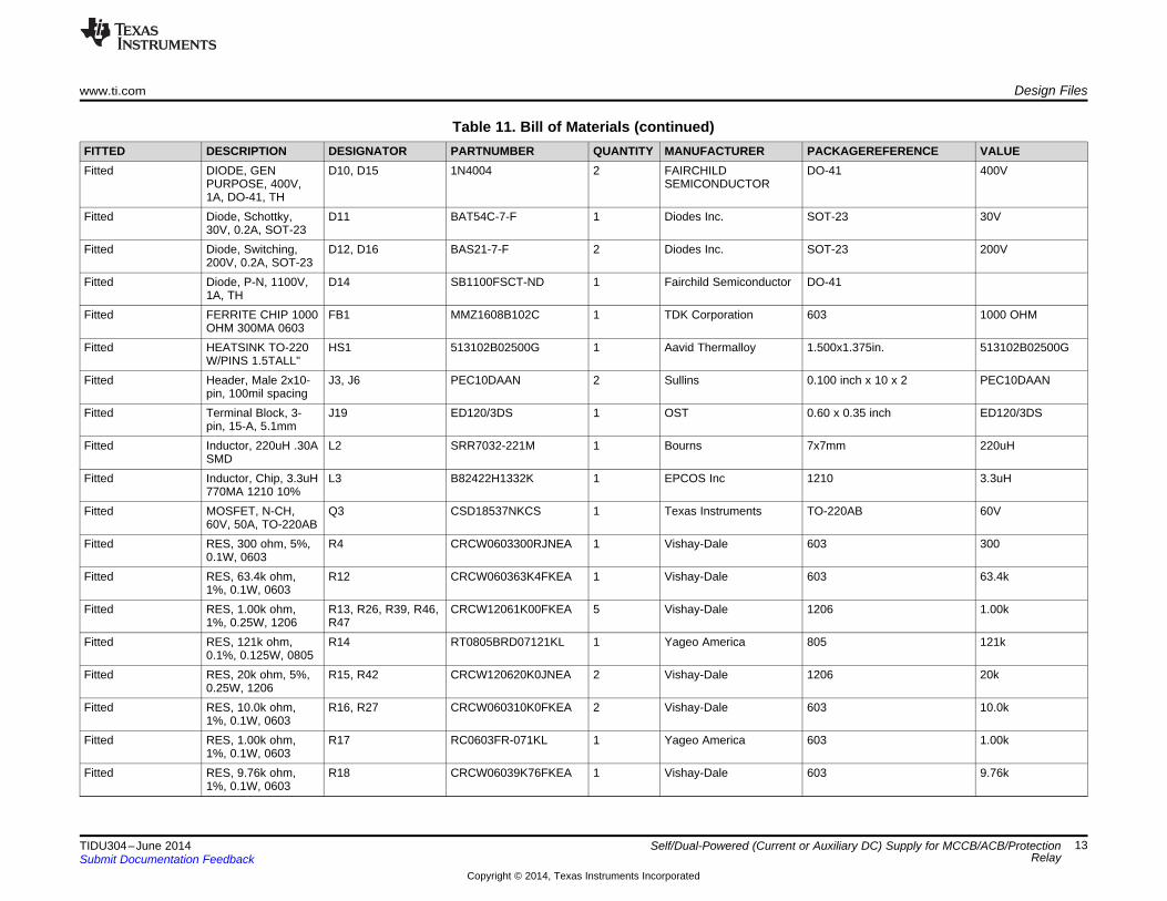
6.2 Bill of MaterialsTo download the bill of materials (BOM), see the design files at TIDA-00229. To see the BOM for the Fitted category, see Table 11.
Table 11. Bill of Materials
FITTED DESCRIPTION DESIGNATOR PARTNUMBER QUANTITY MANUFACTURER PACKAGEREFERENCE VALUEFitted CAP, CERM, 0.1uF, C5, C9, C30 C0603C104K5RACTU 3 Kemet 603 0.1uF
50V, +/-10%, X7R,0603
Fitted CAP, CERM, 1uF, C6, C7 C1608X7R1C105K 2 TDK 603 1uF16V, +/-10%, X7R,0603
Fitted CAP, CERM, 22uF, C8 GRM31CR61C226KE15 1 MuRata 1206 22uF16V, +/-10%, X5R, L1206
Fitted CAP, TA, 4.7uF, C11 293D475X9035C2TE3 1 Vishay-Sprague 6032-28 4.7uF35V, +/-10%, 1.9ohm, SMD
Fitted CAP, CERM, 1uF, C15 GRM31CR72A105KA01L 1 MuRata 1206 1uF100V, +/-10%, X7R,1206
Fitted CAP, CERM, 0.1uF, C17, C24 C0805C104K1RACTU 2 Kemet 805 0.1uF100V, +/-10%, X7R,0805
Fitted CAP, CERM, 0.01uF, C18 C1608C0G1E103J 1 TDK 603 0.01uF25V, +/-5%,C0G/NP0, 0603
Fitted CAP, CERM, C19 C0603C332K5RACTU 1 Kemet 603 3300pF3300pF, 50V, +/-10%, X7R, 0603
Fitted CAP, CERM, 1uF, C20 C1608X5R1E105K080A 1 TDK 603 1uF25V, +/-10%, X5R, C0603
Fitted CAP, CERM, 0.1uF, C21, C34 06033C104JAT2A 2 AVX 603 0.1uF25V, +/-5%, X7R,0603
Fitted CAP, AL, 100uF, C28 100YXJ100M10X20 1 Rubycon 10x20mm 100uF100V, +/-20%, 0.12ohm, TH
Fitted LED SmartLED D3 LG L29K-G2J1-24-Z 1 OSRAM 603 GreenGreen 570NM
Fitted Diode, Zener, 39V, D8 1N4754A-TP 1 Micro Commercial Co DO-41 1N4754A-TP1W, DO41
Fitted Diode, Zener, 16V, D9 1N4745A-TP 1 Micro Commercial Co DO-41 1N4745A-TP1W, DO41
12 Self/Dual-Powered (Current or Auxiliary DC) Supply for MCCB/ACB/Protection TIDU304–June 2014Relay Submit Documentation Feedback
Copyright © 2014, Texas Instruments Incorporated
www.ti.com Design Files
Table 11. Bill of Materials (continued)FITTED DESCRIPTION DESIGNATOR PARTNUMBER QUANTITY MANUFACTURER PACKAGEREFERENCE VALUEFitted DIODE, GEN D10, D15 1N4004 2 FAIRCHILD DO-41 400V
PURPOSE, 400V, SEMICONDUCTOR1A, DO-41, TH
Fitted Diode, Schottky, D11 BAT54C-7-F 1 Diodes Inc. SOT-23 30V30V, 0.2A, SOT-23
Fitted Diode, Switching, D12, D16 BAS21-7-F 2 Diodes Inc. SOT-23 200V200V, 0.2A, SOT-23
Fitted Diode, P-N, 1100V, D14 SB1100FSCT-ND 1 Fairchild Semiconductor DO-411A, TH
Fitted FERRITE CHIP 1000 FB1 MMZ1608B102C 1 TDK Corporation 603 1000 OHMOHM 300MA 0603
Fitted HEATSINK TO-220 HS1 513102B02500G 1 Aavid Thermalloy 1.500x1.375in. 513102B02500GW/PINS 1.5TALL"
Fitted Header, Male 2x10- J3, J6 PEC10DAAN 2 Sullins 0.100 inch x 10 x 2 PEC10DAANpin, 100mil spacing
Fitted Terminal Block, 3- J19 ED120/3DS 1 OST 0.60 x 0.35 inch ED120/3DSpin, 15-A, 5.1mm
Fitted Inductor, 220uH .30A L2 SRR7032-221M 1 Bourns 7x7mm 220uHSMD
Fitted Inductor, Chip, 3.3uH L3 B82422H1332K 1 EPCOS Inc 1210 3.3uH770MA 1210 10%
Fitted MOSFET, N-CH, Q3 CSD18537NKCS 1 Texas Instruments TO-220AB 60V60V, 50A, TO-220AB
Fitted RES, 300 ohm, 5%, R4 CRCW0603300RJNEA 1 Vishay-Dale 603 3000.1W, 0603
Fitted RES, 63.4k ohm, R12 CRCW060363K4FKEA 1 Vishay-Dale 603 63.4k1%, 0.1W, 0603
Fitted RES, 1.00k ohm, R13, R26, R39, R46, CRCW12061K00FKEA 5 Vishay-Dale 1206 1.00k1%, 0.25W, 1206 R47
Fitted RES, 121k ohm, R14 RT0805BRD07121KL 1 Yageo America 805 121k0.1%, 0.125W, 0805
Fitted RES, 20k ohm, 5%, R15, R42 CRCW120620K0JNEA 2 Vishay-Dale 1206 20k0.25W, 1206
Fitted RES, 10.0k ohm, R16, R27 CRCW060310K0FKEA 2 Vishay-Dale 603 10.0k1%, 0.1W, 0603
Fitted RES, 1.00k ohm, R17 RC0603FR-071KL 1 Yageo America 603 1.00k1%, 0.1W, 0603
Fitted RES, 9.76k ohm, R18 CRCW06039K76FKEA 1 Vishay-Dale 603 9.76k1%, 0.1W, 0603
13TIDU304–June 2014 Self/Dual-Powered (Current or Auxiliary DC) Supply for MCCB/ACB/ProtectionRelaySubmit Documentation Feedback
Copyright © 2014, Texas Instruments Incorporated

Design Files www.ti.com
Table 11. Bill of Materials (continued)FITTED DESCRIPTION DESIGNATOR PARTNUMBER QUANTITY MANUFACTURER PACKAGEREFERENCE VALUEFitted RES, 53.6k ohm, R19 RG2012P-5362-B-T5 1 Susumu Co Ltd 805 53.6k
0.1%, 0.125W, 0805Fitted RES, 10.0k ohm, R25, R28, R37 CRCW120610K0FKEA 3 Vishay-Dale 1206 10.0k
1%, 0.25W, 1206Fitted RES, 1.00Meg ohm, R40, R73 CRCW06031M00FKEA 2 Vishay-Dale 603 1.00Meg
1%, 0.1W, 0603Fitted RES, 10k ohm, R41, R70, R71, R72 RNCF0603TKY10K0 4 Stackpole Electronics Inc 603 10k
0.01%, 0.063W,0603
Fitted RES, 510 ohm, R48 RG1608P-511-B-T5 1 Susumu Co Ltd 603 5100.1%, 0.1W, 0603
Fitted RES, 0 ohm, 5%, R75, R78 CRCW06030000Z0EA 2 Vishay-Dale 603 00.1W, 0603
Fitted RES, 47k ohm, 5%, R82 ERJ-6GEYJ473V 1 Panasonic 805 47k0.125W, 0805
Fitted Test Point, O.040 TP16, TP18, TP22, STD 4 STD STDHole TP31
Fitted IC, 300-mA 40-V U1 TPS7A6533QKVURQ1 1 TI PFM TPS7A6533QKVULOW-DROPOUT RQ1REGULATOR WITH25-uA QUIESCENTCURRENT
Fitted 100V, 600mA U3 LM5017MRE/NOPB 1 Texas Instruments DDA0008BConstant On-TimeSynchronous BuckRegulator,DDA0008B
Fitted IC, Dual Differential U5 LM293AD 1 TI SO-8 LM293ADComparators, 2-36Vin
14 Self/Dual-Powered (Current or Auxiliary DC) Supply for MCCB/ACB/Protection TIDU304–June 2014Relay Submit Documentation Feedback
Copyright © 2014, Texas Instruments Incorporated

www.ti.com Design Files
6.3 Layer PlotsTo download the layer plots for this design, see the design files at TIDA-00229.
Figure 5 through Figure 10 show the layer plots for this design.
NOTE: All layer plots are viewed from the top side.
Figure 5. Solder Mask Top Figure 6. Solder Mask Bottom
Figure 7. Top Layer Figure 8. Bottom Layer
15TIDU304–June 2014 Self/Dual-Powered (Current or Auxiliary DC) Supply forMCCB/ACB/Protection RelaySubmit Documentation Feedback
Copyright © 2014, Texas Instruments Incorporated

Design Files www.ti.com
Figure 9. Top Overlay Figure 10. Bottom Overlay
6.4 Multilayer Composite PrintsTo download the Multilayer Composite Print files, see the design files at TIDA-00229.
Figure 11. Multilayer Composite Print
16 Self/Dual-Powered (Current or Auxiliary DC) Supply for TIDU304–June 2014MCCB/ACB/Protection Relay Submit Documentation Feedback
Copyright © 2014, Texas Instruments Incorporated

www.ti.com Design Files
6.5 Assembly DrawingsTo download the Assembly Drawings, see the design files at TIDA-00229.
Figure 12. Assembly Drawing 1 Figure 13. Assembly Drawing 2
Figure 14. Assembly Drawing 3 Figure 15. Assembly Drawing 4
17TIDU304–June 2014 Self/Dual-Powered (Current or Auxiliary DC) Supply forMCCB/ACB/Protection RelaySubmit Documentation Feedback
Copyright © 2014, Texas Instruments Incorporated

Design Files www.ti.com
Figure 16. Drill Drawing
6.6 Gerber FilesTo download the Gerber files, see the design files at TIDA-00229.
7 About the AuthorKALLIKUPPA MUNIYAPPA SREENIVASA is a Systems Architect at Texas Instruments, where he isresponsible for developing reference design solutions for the industrial segment. Sreenivasa brings to thisrole his experience in high-speed digital and analog systems design. Sreenivasa earned his Bachelor ofElectronics (BE) in Electronics and communication Engineering (BE-E&C) from VTU, Mysore, India.
18 Self/Dual-Powered (Current or Auxiliary DC) Supply for TIDU304–June 2014MCCB/ACB/Protection Relay Submit Documentation Feedback
Copyright © 2014, Texas Instruments Incorporated

IMPORTANT NOTICE FOR TI REFERENCE DESIGNS
Texas Instruments Incorporated ("TI") reference designs are solely intended to assist designers (“Buyers”) who are developing systems thatincorporate TI semiconductor products (also referred to herein as “components”). Buyer understands and agrees that Buyer remainsresponsible for using its independent analysis, evaluation and judgment in designing Buyer’s systems and products.TI reference designs have been created using standard laboratory conditions and engineering practices. TI has not conducted anytesting other than that specifically described in the published documentation for a particular reference design. TI may makecorrections, enhancements, improvements and other changes to its reference designs.Buyers are authorized to use TI reference designs with the TI component(s) identified in each particular reference design and to modify thereference design in the development of their end products. HOWEVER, NO OTHER LICENSE, EXPRESS OR IMPLIED, BY ESTOPPELOR OTHERWISE TO ANY OTHER TI INTELLECTUAL PROPERTY RIGHT, AND NO LICENSE TO ANY THIRD PARTY TECHNOLOGYOR INTELLECTUAL PROPERTY RIGHT, IS GRANTED HEREIN, including but not limited to any patent right, copyright, mask work right,or other intellectual property right relating to any combination, machine, or process in which TI components or services are used.Information published by TI regarding third-party products or services does not constitute a license to use such products or services, or awarranty or endorsement thereof. Use of such information may require a license from a third party under the patents or other intellectualproperty of the third party, or a license from TI under the patents or other intellectual property of TI.TI REFERENCE DESIGNS ARE PROVIDED "AS IS". TI MAKES NO WARRANTIES OR REPRESENTATIONS WITH REGARD TO THEREFERENCE DESIGNS OR USE OF THE REFERENCE DESIGNS, EXPRESS, IMPLIED OR STATUTORY, INCLUDING ACCURACY ORCOMPLETENESS. TI DISCLAIMS ANY WARRANTY OF TITLE AND ANY IMPLIED WARRANTIES OF MERCHANTABILITY, FITNESSFOR A PARTICULAR PURPOSE, QUIET ENJOYMENT, QUIET POSSESSION, AND NON-INFRINGEMENT OF ANY THIRD PARTYINTELLECTUAL PROPERTY RIGHTS WITH REGARD TO TI REFERENCE DESIGNS OR USE THEREOF. TI SHALL NOT BE LIABLEFOR AND SHALL NOT DEFEND OR INDEMNIFY BUYERS AGAINST ANY THIRD PARTY INFRINGEMENT CLAIM THAT RELATES TOOR IS BASED ON A COMBINATION OF COMPONENTS PROVIDED IN A TI REFERENCE DESIGN. IN NO EVENT SHALL TI BELIABLE FOR ANY ACTUAL, SPECIAL, INCIDENTAL, CONSEQUENTIAL OR INDIRECT DAMAGES, HOWEVER CAUSED, ON ANYTHEORY OF LIABILITY AND WHETHER OR NOT TI HAS BEEN ADVISED OF THE POSSIBILITY OF SUCH DAMAGES, ARISING INANY WAY OUT OF TI REFERENCE DESIGNS OR BUYER’S USE OF TI REFERENCE DESIGNS.TI reserves the right to make corrections, enhancements, improvements and other changes to its semiconductor products and services perJESD46, latest issue, and to discontinue any product or service per JESD48, latest issue. Buyers should obtain the latest relevantinformation before placing orders and should verify that such information is current and complete. All semiconductor products are soldsubject to TI’s terms and conditions of sale supplied at the time of order acknowledgment.TI warrants performance of its components to the specifications applicable at the time of sale, in accordance with the warranty in TI’s termsand conditions of sale of semiconductor products. Testing and other quality control techniques for TI components are used to the extent TIdeems necessary to support this warranty. Except where mandated by applicable law, testing of all parameters of each component is notnecessarily performed.TI assumes no liability for applications assistance or the design of Buyers’ products. Buyers are responsible for their products andapplications using TI components. To minimize the risks associated with Buyers’ products and applications, Buyers should provideadequate design and operating safeguards.Reproduction of significant portions of TI information in TI data books, data sheets or reference designs is permissible only if reproduction iswithout alteration and is accompanied by all associated warranties, conditions, limitations, and notices. TI is not responsible or liable forsuch altered documentation. Information of third parties may be subject to additional restrictions.Buyer acknowledges and agrees that it is solely responsible for compliance with all legal, regulatory and safety-related requirementsconcerning its products, and any use of TI components in its applications, notwithstanding any applications-related information or supportthat may be provided by TI. Buyer represents and agrees that it has all the necessary expertise to create and implement safeguards thatanticipate dangerous failures, monitor failures and their consequences, lessen the likelihood of dangerous failures and take appropriateremedial actions. Buyer will fully indemnify TI and its representatives against any damages arising out of the use of any TI components inBuyer’s safety-critical applications.In some cases, TI components may be promoted specifically to facilitate safety-related applications. With such components, TI’s goal is tohelp enable customers to design and create their own end-product solutions that meet applicable functional safety standards andrequirements. Nonetheless, such components are subject to these terms.No TI components are authorized for use in FDA Class III (or similar life-critical medical equipment) unless authorized officers of the partieshave executed an agreement specifically governing such use.Only those TI components that TI has specifically designated as military grade or “enhanced plastic” are designed and intended for use inmilitary/aerospace applications or environments. Buyer acknowledges and agrees that any military or aerospace use of TI components thathave not been so designated is solely at Buyer's risk, and Buyer is solely responsible for compliance with all legal and regulatoryrequirements in connection with such use.TI has specifically designated certain components as meeting ISO/TS16949 requirements, mainly for automotive use. In any case of use ofnon-designated products, TI will not be responsible for any failure to meet ISO/TS16949.
Mailing Address: Texas Instruments, Post Office Box 655303, Dallas, Texas 75265Copyright © 2014, Texas Instruments Incorporated
Related Documents