Submitted by Andreas Gebhard Submitted at Institute of Signal Processing Supervisor and First Examiner Univ.-Prof. Dr. Mario Huemer Second Examiner Prof. Dr.-Ing. Bin Yang Co-Supervisors - April 2019 JOHANNES KEPLER UNIVERSITY LINZ Altenbergerstraße 69 4040 Linz, ¨ Osterreich www.jku.at DVR 0093696 Self-Interference Cancellation and Rejection in FDD RF-Transceivers Doctoral Thesis to obtain the academic degree of Doktor der technischen Wissenschaften in the Doctoral Program Technische Wissenschaften

Welcome message from author
This document is posted to help you gain knowledge. Please leave a comment to let me know what you think about it! Share it to your friends and learn new things together.
Transcript
Submitted byAndreas Gebhard
Submitted atInstitute ofSignal Processing
Supervisor andFirst ExaminerUniv.-Prof. Dr.Mario Huemer
Second ExaminerProf. Dr.-Ing.Bin Yang
Co-Supervisors-
April 2019
JOHANNES KEPLERUNIVERSITY LINZAltenbergerstraße 694040 Linz, Osterreichwww.jku.atDVR 0093696
Self-Interference Cancellation andRejection in FDD RF-Transceivers
Doctoral Thesis
to obtain the academic degree of
Doktor der technischen Wissenschaften
in the Doctoral Program
Technische Wissenschaften

Abstract
Modern mobile communication devices offer a variety of data intensive services likevideo telephony or multimedia streaming. To support the high data rates needed forthese services, the 3rd Generation Partnership Project (3GPP) introduced Long TermEvolution-Advanced (LTE-A) which includes the carrier aggregation (CA) feature. WithCA, multiple parts of the spectrum which are scattered across the frequency bands maybe aggregated to increase the data throughput. LTE-A supports the frequency divisionduplex (FDD) operation for simultaneous transmission and reception in over 40 fre-quency bands. For each operating band a separate band-pass filter (duplexer) is neededto provide isolation between the transmitters and the receivers which is a driving costfactor within the analog front-end of the transceiver. Consequently, in cost effectivefront-ends duplexers with reduced isolation are used. The resulting transmitter leakagesignal into the CA receivers in combination with front-end non-idealities leads to a re-ceiver desensitization.
In this dissertation three major contributions are provided. As a first step, the transmitterleakage (TxL) signal caused receiver interferences are modeled in the radio frequency(RF) domain and the resulting baseband (BB) equivalent receiver interferences are de-termined. This includes the modeling of the modulated spur-, and the second-orderintermodulation distortion (IMD2) interference. The down-conversion of the TxL signalby spurs creates the modulated spur interference which may consist of a main and animage component. The second-order nonlinearity of the mixer creates an IMD2 interfer-ence which always falls around the zero-frequency. In case of direct-conversion receiverarchitectures, this leads to a BB interference which disturbs the wanted receive signal.Furthermore, the 25% duty-cycle current driven passive mixer which is preferably used indirect-conversion receivers is modeled. Due to the square-wave control signals, harmon-ics are produced within the mixer which may lead to the down-conversion of unwantedspectral components into the receiver BB. This down-conversion by the harmonic re-sponse of the mixer may degrade the receiver performance.
In a second step, the BB equivalent interference models are used to derive dedicatedadaptive filters to cancel the TxL signal caused self-interferences in the digital BB of thetransceiver. This dissertation provides solutions to cancel the modulated spur-, and theIMD2 interference by adaptive filtering. Simulation results show that a widely-linearadaptive filter structure is able to cancel the main-, and image modulated spur inter-ference. A major part of this thesis investigates solutions for the digital cancellationof the IMD2 interference. Nonlinear Wiener model least-mean-squares (LMS)-, andrecursive-least-squares (RLS) based adaptive filters are developed which outperform thetraditional Volterra kernel based adaptive filters in terms of performance and complex-ity. The functionality of the proposed nonlinear adaptive filters is demonstrated usingsimulated and measured IMD2 data.
I

The third contribution is the development of a harmonic rejection mixer concept for the25% duty-cycle current driven passive mixer. With this approach, the down-conversionof blocker signals by the harmonic response of the mixer can be suppressed. Circuitsimulations using a 28 nm technology package show a superior suppression of the mixerharmonic response.

Kurzfassung
Moderne mobile Kommunikationssysteme ermoglichen eine Vielzahl datenintensiverAnwendungen wie etwa die Videotelefonie oder das Streamen von Multimedia-Inhalten.Um die fur diese Anwendungen erforderlichen Datenraten bereitzustellen wurde vomStandardisierungsgremium 3GPP der LTE-A Standard eingefuhrt welcher u.a. das soge-nannte Carrier Aggregation (CA) ermoglicht. Mit Hilfe von CA konnen mehrere verteilteAnteile des Kommunikationsspektrums vereint werden um eine hohere Datenrate zuerreichen. LTE-A unterstutzt das Frequenzmultiplexverfahren welches das simultaneSenden und Empfangen von Daten in uber 40 Frequenzbandern ermoglicht. Fur jedesFrequenzband wird ein separates Bandpassfilter zur Isolation zwischen den Sendern undden Empfangern benotigt was ein treibender Kostenfaktor fur das analoge Front-End ist.Somit werden in kosteneffizienten Front-Ends Bandpassfilter mit reduzierter Dampfungeingesetzt um die Kosten zu senken. Daraus resultierend ergibt sich ein Lecksignal vomSender in jeden einzelnen CA Empfanger welches in Kombination mit Nichtidealitatendes Front-Ends zu einer Desensibilisierung der Empfanger fuhrt.
Diese Dissertation liefert drei wesentliche Beitrage. Der erste Beitrag besteht aus derModellierung der Storungen im Empfanger welche durch das Lecksignal und die Front-End Nichtidealitaten erzeugt werden. Dabei wird ausgehend von den Nichtidealitatenim Hochfrequenzbereich ein Basisband-aquivalentes Modell der Storungen hergeleitet.Zu den modellierten Storungen zahlen u.a. die Modulated Spur Interferenz und Inter-modulationsprodukte zweiter Ordnung. Die Modulated Spur Interferenz wird erzeugtindem das Lecksignal des Senders durch sogenannte Spurs in das Empfanger Basis-band heruntergemischt wird. Hierbei kommt es aufgrund der IQ Imbalance der Spursneben der Haupt-Interferenz auch zu einer zusatzlichen Bild-Interferenz. Die Nicht-linearitat zweiter Ordnung des Mischers erzeugt ein Intermodulationsprodukt welchesimmer um die Null-Frequenz fallt. Bei Verwendung eines Homodynempfangers fuhrtdies zu einer Storung des gewunschten Empfangssignals. Auch der in der Stromdomanebetriebene Mischer, der mit Rechtecksignalen und dem Tastverhaltnis von 25% arbeitetund vorzugsweise in Homodynempfangern zum Einsatz kommt, wird modelliert. Durchdie verwendeten Rechtecksignale, die zur Ansteuerung des Mischers verwendet werden,entstehen Harmonische welche unerwunschte Signalkomponenten ins Basisband mischenund somit die Empfangerempfindlichkeit reduzieren.
Im zweiten Beitrag werden die Basisband-aquivalenten Modelle der Storungen zur Her-leitung dedizierter adaptiver Filter verwendet mit deren Hilfe die Storungen vom Emp-fangssignal herausgerechnet werden konnen. In dieser Dissertation werden adaptiveFilter zur Unterdruckung der Modulated Spur Interferenz und von Intermodulation-sprodukten zweiter Ordnung entwickelt. In Simulationen wird gezeigt, dass durch eineErweiterung des adaptiven Filters beide Storkomponenten der Modulated Spur Inter-ferenz unterdruckt werden konnen. Ein großer Teil der Arbeit behandelt Methoden zurUnterdruckung von Intermodulationsprodukten zweiter Ordnung durch adaptive Fil-terung im Basisband des Transceivers. Hierfur wurden zwei nichtlineare Algorithmenentwickelt die auf dem LMS-, und dem RLS Algorithmus basieren. Diese Algorithmenverwenden das nichtlineare Wiener Modell, und sind in der Lage traditionelle Algorith-men, die auf dem Volterra Modell basieren in Bezug auf Konvergenzgeschwindigkeit
III

und geringerer Komplexitat zu ubertreffen. Die Funktion der entwickelten nichtlinearenadaptiven Algorithmen wurde mit Hilfe von Simulations-, und Messdaten evaluiert.
Im dritten Beitrag wird ein Konzept zur Unterdruckung von Harmonischen in Mischern,welche nach dem 25% Tastverhaltnis arbeiten, prasentiert. Damit kann das Herun-termischen von unerwunschten Storsignalen durch die Harmonischen des Mischer un-terdruckt werden. Das Konzept wird durch Schaltungssimulationen die ein 28 nm Tech-nologiepaket einbinden verifiziert, wobei eine sehr gute Unterdruckung der Harmonischennachgewiesen werden kann.

Statutory Declaration
I hereby declare that the thesis submitted is my own unaided work, that I have notused other than the sources indicated, and that all direct and indirect sources are ac-knowledged as references. This printed thesis is identical with the electronic versionsubmitted.
V


Acknowledgements
First, I would like to express my sincere gratitude to my supervisor Univ.-Prof. Dr.Mario Huemer for giving me the opportunity to write my PhD thesis at the Instituteof Signal Processing at the Johannes Kepler University Linz. I would like to thank himfor the fruitful technical discussions which increased the quality of our publications, mythesis and finally our research.
I wish to thank Thomas Buchegger who supported my wish of starting a PhD thesiswhile I was working in his team at the Linz Center of Mechatronics (LCM). My deepgratitude goes to my colleagues at the Institute of Signal Processing for their great teamspirit and the numerous technical discussions which we had.
I thank the self-interference cancellation (SIC) team of our Christian-Doppler Labo-ratory (CD-Lab) for the great collaboration, and particularly I would like to express mygratitude to Christian Motz for reviewing my draft version of the thesis. Furthermore, Iwould like to thank all members of the CD-Lab for their collaboration and the inspiringworking environment. A big thank you goes out to Matthias Wagner who establishedthe RF measurement station at the institute. I also want to thank Alexander Gruber forhis support in doing measurements at the RF transceiver chip of the industrial partner.
I want to thank Michael Lunglmayr for becoming a good friend and for his supportin even non-technical (mostly LaTex related) issues. I also would like to express my sin-cere gratitude to Ram Sunil Kanumalli and Silvester Sadjina for the great collaborationduring our PhD period and for becoming great friends.
I would like to thank my family and especially my father for supporting me in all myprojects. Finally, I want to thank my wife Nadine for her support during my PhD periodand for being a great mother for our son Noah.
VII

I wish to acknowledge DMCE GmbH & Co KG as part of Intel for supporting this workcarried out at the Christian Doppler Laboratory for Digitally Assisted RF Transceiversfor Future Mobile Communications. The financial support by the Austrian FederalMinistry for Digital and Economic Affairs and the National Foundation for Research,Technology and Development is gratefully acknowledged.

Engineers should be able to act nonlinearly and are expected to have good memory.This is just the opposite from what an engineer wants from a system.
- Myself
IX

Contents
1 Introduction 11.1 Mobile Communication Devices . . . . . . . . . . . . . . . . . . . . . . . . 1
1.2 Functionality of an FDD CA Transceiver . . . . . . . . . . . . . . . . . . . 2
1.3 Transmitter Leakage Induced Self-Interferences . . . . . . . . . . . . . . . 4
1.4 State of the Art . . . . . . . . . . . . . . . . . . . . . . . . . . . . . . . . . 6
1.5 Scope of this Work . . . . . . . . . . . . . . . . . . . . . . . . . . . . . . . 8
2 Interferences in FDD RF Transceivers 132.1 Interference Overview . . . . . . . . . . . . . . . . . . . . . . . . . . . . . 13
2.1.1 Non-Carrier Aggregation Related Interferences . . . . . . . . . . . 14
2.1.2 Rx Carrier Aggregation Related Interference Problems . . . . . . . 15
2.1.3 Tx Carrier Aggregation Related Interference Problems . . . . . . . 19
2.2 Operation of the 25% Duty-Cycle Current-Driven Passive Mixer . . . . . 20
2.3 Self-Interference Modelling . . . . . . . . . . . . . . . . . . . . . . . . . . . 26
2.3.1 Nonlinearity in the Transmitter . . . . . . . . . . . . . . . . . . . . 27
2.3.2 Nonlinearity in the Receiver . . . . . . . . . . . . . . . . . . . . . . 32
2.3.3 Spur IQ-Imbalance . . . . . . . . . . . . . . . . . . . . . . . . . . . 35
2.3.4 Modulated Spur Interference with Spur IQ-Imbalance . . . . . . . 35
2.3.5 Mixer Terminal Coupling Induced IMD2 . . . . . . . . . . . . . . . 37
2.3.6 Higher Even-Order Intermodulation Interferences . . . . . . . . . . 40
2.4 Quantification of the IMD2 Interference . . . . . . . . . . . . . . . . . . . 41
2.4.1 Two-Tone IIP2 Derivation . . . . . . . . . . . . . . . . . . . . . . . 41
2.4.2 Modulated IMD2 Distortion . . . . . . . . . . . . . . . . . . . . . . 43
2.4.3 IIP2 Characterization . . . . . . . . . . . . . . . . . . . . . . . . . 46
2.4.4 Severity of the IMD2 Interference . . . . . . . . . . . . . . . . . . . 46
2.5 Modulated Spurs in Split-LNA Configuration . . . . . . . . . . . . . . . . 47
2.5.1 Phase-Noise Model of the 25% Duty-Cycle Mixer . . . . . . . . . . 49
2.5.2 Spur Modeling . . . . . . . . . . . . . . . . . . . . . . . . . . . . . 49
2.5.3 Modulated Spur with IQ-Imbalance and Tx/Rx PN . . . . . . . . 50
3 Interference Rejection 533.1 Introduction . . . . . . . . . . . . . . . . . . . . . . . . . . . . . . . . . . . 53
3.2 State of the Art . . . . . . . . . . . . . . . . . . . . . . . . . . . . . . . . . 54
3.3 Proposed Harmonic Rejection Control Signals . . . . . . . . . . . . . . . . 55
3.3.1 Proposed Waveform A . . . . . . . . . . . . . . . . . . . . . . . . . 56
3.3.2 Proposed Waveform B . . . . . . . . . . . . . . . . . . . . . . . . . 58
3.4 Circuit Simulation Results . . . . . . . . . . . . . . . . . . . . . . . . . . . 60
4 Adaptive Interference Cancellation 634.1 Introduction . . . . . . . . . . . . . . . . . . . . . . . . . . . . . . . . . . . 63
4.2 Basic Adaptive Filter Structure . . . . . . . . . . . . . . . . . . . . . . . . 63
4.3 Complex Derivatives . . . . . . . . . . . . . . . . . . . . . . . . . . . . . . 65
4.3.1 The Cauchy-Riemann Equations . . . . . . . . . . . . . . . . . . . 65
4.3.2 Adaptive Learning Algorithms . . . . . . . . . . . . . . . . . . . . 65
XI

4.3.3 Wirtinger Derivatives . . . . . . . . . . . . . . . . . . . . . . . . . 66
4.3.4 Iterative Minimization of a Real Valued Cost Function . . . . . . . 67
4.4 The Least-Mean-Squares Algorithm . . . . . . . . . . . . . . . . . . . . . 68
4.5 The Recursive Least-Squares Algorithm . . . . . . . . . . . . . . . . . . . 71
4.6 Modulated Spur Cancellation . . . . . . . . . . . . . . . . . . . . . . . . . 73
4.6.1 Widely-Linear Modulated Spur Cancellation . . . . . . . . . . . . 75
4.6.2 Simulation Results . . . . . . . . . . . . . . . . . . . . . . . . . . . 77
4.6.3 Conclusion . . . . . . . . . . . . . . . . . . . . . . . . . . . . . . . 79
5 Adaptive IMD2 Cancellation 815.1 Introduction . . . . . . . . . . . . . . . . . . . . . . . . . . . . . . . . . . . 81
5.2 State of the Art . . . . . . . . . . . . . . . . . . . . . . . . . . . . . . . . . 82
5.3 Polynomial Filters . . . . . . . . . . . . . . . . . . . . . . . . . . . . . . . 82
5.3.1 Hammerstein Model . . . . . . . . . . . . . . . . . . . . . . . . . . 83
5.3.2 Truncated Volterra Model . . . . . . . . . . . . . . . . . . . . . . . 86
5.4 Wiener Model Based Cancellation . . . . . . . . . . . . . . . . . . . . . . 89
5.4.1 Interference Replica Model . . . . . . . . . . . . . . . . . . . . . . 89
5.4.2 The IMD2 Problem from an Optimization Point of View . . . . . . 91
5.4.3 Multiple Solutions . . . . . . . . . . . . . . . . . . . . . . . . . . . 94
5.4.4 Wiener-Model LMS Based IMD2 Cancellation (IM2LMS) . . . . . 95
5.4.5 Reduced Complexity IM2LMS Algorithm . . . . . . . . . . . . . . 98
5.4.6 Simplified Derivation of the IM2LMS Algorithm . . . . . . . . . . 101
5.4.7 Wiener-Model RLS Based IMD2 Cancellation (IM2RLS) . . . . . . 103
5.4.8 Incorporating the Estimation of the Q-Path IMD2 Interference . . 111
5.4.9 Complexity Comparison . . . . . . . . . . . . . . . . . . . . . . . . 111
5.5 Simulation Results . . . . . . . . . . . . . . . . . . . . . . . . . . . . . . . 114
5.5.1 LMS Based IMD2 Cancellation . . . . . . . . . . . . . . . . . . . . 114
5.5.2 RLS Based IMD2 Cancellation . . . . . . . . . . . . . . . . . . . . 117
5.6 Verification with Measured Data . . . . . . . . . . . . . . . . . . . . . . . 121
5.6.1 Measurements from the Transceiver Chip . . . . . . . . . . . . . . 121
5.6.2 Measurement Setup with Discrete RF Components . . . . . . . . . 124
5.7 Conclusion . . . . . . . . . . . . . . . . . . . . . . . . . . . . . . . . . . . 127
6 Conclusion and Outlook 129
A Appendix 131A.1 Power Spectral Density Plots . . . . . . . . . . . . . . . . . . . . . . . . . 131
A.2 Spur Generation in 25% Duty-Cycle Mixers with the Split-LNA Configu-ration . . . . . . . . . . . . . . . . . . . . . . . . . . . . . . . . . . . . . . 131
A.3 Receiver Noise Floor . . . . . . . . . . . . . . . . . . . . . . . . . . . . . . 134
A.4 Scaling of Complex Baseband Signals for a Desired Power Level, SNR andSINR . . . . . . . . . . . . . . . . . . . . . . . . . . . . . . . . . . . . . . . 135
A.4.1 Complex White Gaussian Noise . . . . . . . . . . . . . . . . . . . . 135
A.4.2 Generation of an Rx Signal with Desired Power Level . . . . . . . 135
A.4.3 Generation of an Rx Signal with Desired SNR . . . . . . . . . . . 136
A.4.4 Generation of an Rx Signal with Desired SINR . . . . . . . . . . . 136
A.5 Derivative of a Channel-Select Filtered Signal . . . . . . . . . . . . . . . . 137
XII

List of Abbreviations 141
Bibliography 143
Curriculum Vitae 151
XIII

1Introduction
1.1 Mobile Communication Devices
Modern mobile communication devices such as smartphones are enabling multiple ser-vices for the consumer. Starting from global positioning for navigation purposes, videostreaming, internet browsing, fitness tracking and social networks, the smartphone be-comes a device which is indispensable. However, the use of smartphones for traditionalvoice calls and text messages is faded into the background. This variety of services,especially the data intensive ones as multimedia streaming and video-telephony led toan enormous increase of data traffic. To satisfy this need for higher data rates LongTerm Evolution-Advanced (LTE-A) was introduced in the 3rd Generation PartnershipProject (3GPP) Release 10 [1], which offers the carrier aggregation (CA) feature. Thisenables the aggregation of multiple parts of the spectrum (component carriers (CC)) toincrease the effective data rate. This CCs may be scattered across the spectrum due tothe fact that the available bandwidth was distributed by auctions between the mobileoperators. Therefore, to offer the CA feature to the customers the mobile device hasto be prepared to receive/transmit data from a scattered spectral environment. LTE-Asupports the frequency division duplex (FDD) operation for simultaneous transmissionand reception of data at different frequencies. To increase the data rate the FDD oper-ation is combined with the CA feature. Also the time-division duplex (TDD) mode issupported where data is transmitted or received alternately at the same frequency.
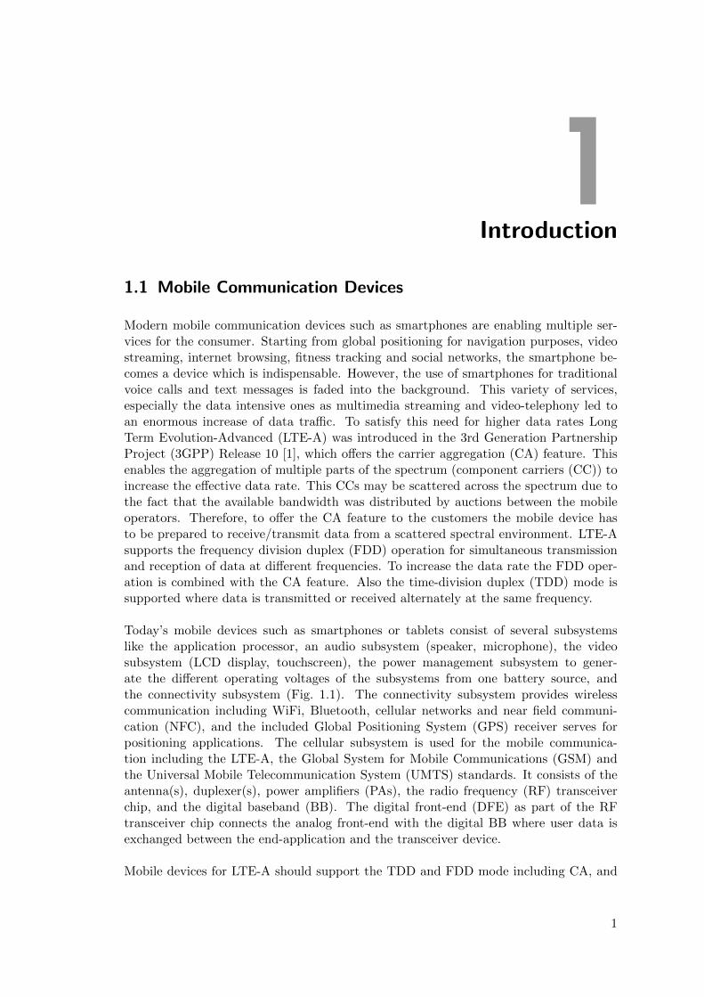
Today’s mobile devices such as smartphones or tablets consist of several subsystemslike the application processor, an audio subsystem (speaker, microphone), the videosubsystem (LCD display, touchscreen), the power management subsystem to gener-ate the different operating voltages of the subsystems from one battery source, andthe connectivity subsystem (Fig. 1.1). The connectivity subsystem provides wirelesscommunication including WiFi, Bluetooth, cellular networks and near field communi-cation (NFC), and the included Global Positioning System (GPS) receiver serves forpositioning applications. The cellular subsystem is used for the mobile communica-tion including the LTE-A, the Global System for Mobile Communications (GSM) andthe Universal Mobile Telecommunication System (UMTS) standards. It consists of theantenna(s), duplexer(s), power amplifiers (PAs), the radio frequency (RF) transceiverchip, and the digital baseband (BB). The digital front-end (DFE) as part of the RFtransceiver chip connects the analog front-end with the digital BB where user data isexchanged between the end-application and the transceiver device.
Mobile devices for LTE-A should support the TDD and FDD mode including CA, and
1
1 Introduction
Mobile DevicePower
Management
AudioSubsystem
ApplicationProcessor
DisplaySubsystem
ConnectivitySubsystem
Memory
WiFi
Bluetooth
GPS
Cellular (2G, 3G, 4G)
TransceiverBaseband
LNA
LNA
PA
CSF
CSF
AD
A
D
A
D
Antenna
Duplexer
DFE
fRx2
fRx1
fTx Transceiver chip
Tx
Rx1
Rx2
Figure 1.1: Block diagram of a typical mobile device.
the operation in multiple frequency bands to access the scattered spectrum. But restric-tions like power consumption and costs are driving design parameters for the transceiverchip architecture. The transceiver contains the transmitter(s) and the receiver(s), andtherefore enables the exchange of data between the base-stations and the mobile device.The direct-conversion receiver architecture (also known as zero-intermediate frequency(IF)-, or homodyne receiver) [2] is mainly used in modern transceivers due to the lowerpower consumption and the lower hardware complexity compared to e.g. low-IF re-ceivers. In this architecture, the wanted receive (Rx) signal is directly down-convertedfrom the RF to the BB (zero-frequency). In this way the required sampling frequency todigitize the signal is kept at the minimum which saves power. Also for the transmittersdirect conversion architectures are frequently used.
1.2 Functionality of an FDD CA Transceiver
The FDD operation mode which is used in Long Term Evolution (LTE) has the advan-tage that data can be simultaneously transmitted and received at different frequenciesover one common antenna. This is enabled by the frequency-selectivity of the analogfront-end (duplexers). In Fig. 1.1 an RF transceiver with two CA receivers and onetransmitter is depicted. The operating frequency fRx1 of receiver Rx1 (primary re-ceiver) is related to the transmitter operating frequency fTx via the duplexing distance.
2
1.2 Functionality of an FDD CA Transceiver
Component carrier with 1.4/3/5/15/20 MHz bandwidth
Allocated recource blocks
Non-allocated recource blocks
Intra-band CA withcontiguous CCs
Intra-band CA withnon-contiguous CCs
Inter-band CA
f
f
f
band A
band A
band A
band B
band B
band B
Figure 1.2: Different types of CA.
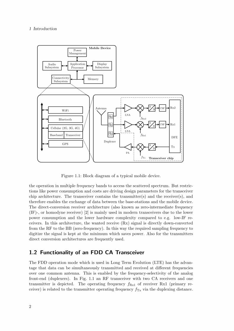
As an example, if LTE band 5 is used with fTx = 831 MHz, then fRx1 = 876 MHzwhich corresponds to the duplexing distance of 45 MHz. Usually in mobile user equip-ments (UEs) the transmit (Tx) frequency is lower than the Rx frequency because thegeneration of a transmit signal at a lower frequency consumes less power. The operatingfrequency of the secondary receiver Rx2 (in LTE-A up to five secondary receivers maybe aggregated using CA) is not coupled to the primary transmit frequency and maybe located at any different frequency depending on the intra/inter-band CA combina-tion [3]. In LTE-A three types of CA are defined which are visualized in Fig. 1.2. Inthe first CA scenario, the intra-band contiguous CA, the aggregated CCs are next toeach other and within the same LTE band. Both aggregated CCs may be received byone receiver if the receive center-frequency is set between the CCs and the samplingfrequency is increased according to the overall bandwidth. The second CA scenariois the intra-band non-contiguous CA where the aggregated CCs are within the sameLTE band but separated by a frequency gap. In this scenario, usually a split-low noiseamplifier (LNA) configuration is used where each receiver is configured to receive oneCC. As we will see later, this configuration using a split-LNA is prone to transmitterleakage self-interference (modulated-spur interference in split-LNA configuration) dueto the limited Tx-to-Rx (duplexer) isolation. In the third CA scenario, the inter-bandCA, the CCs are in different LTE bands. In this case each receiver uses its own LNA(no split-LNA is used) to amplify the received signal as depicted in Fig. 1.1. Also inthis configuration the mentioned modulated-spur interference may occur. However, it iscaused by a different mechanism as will be described in the next sections.
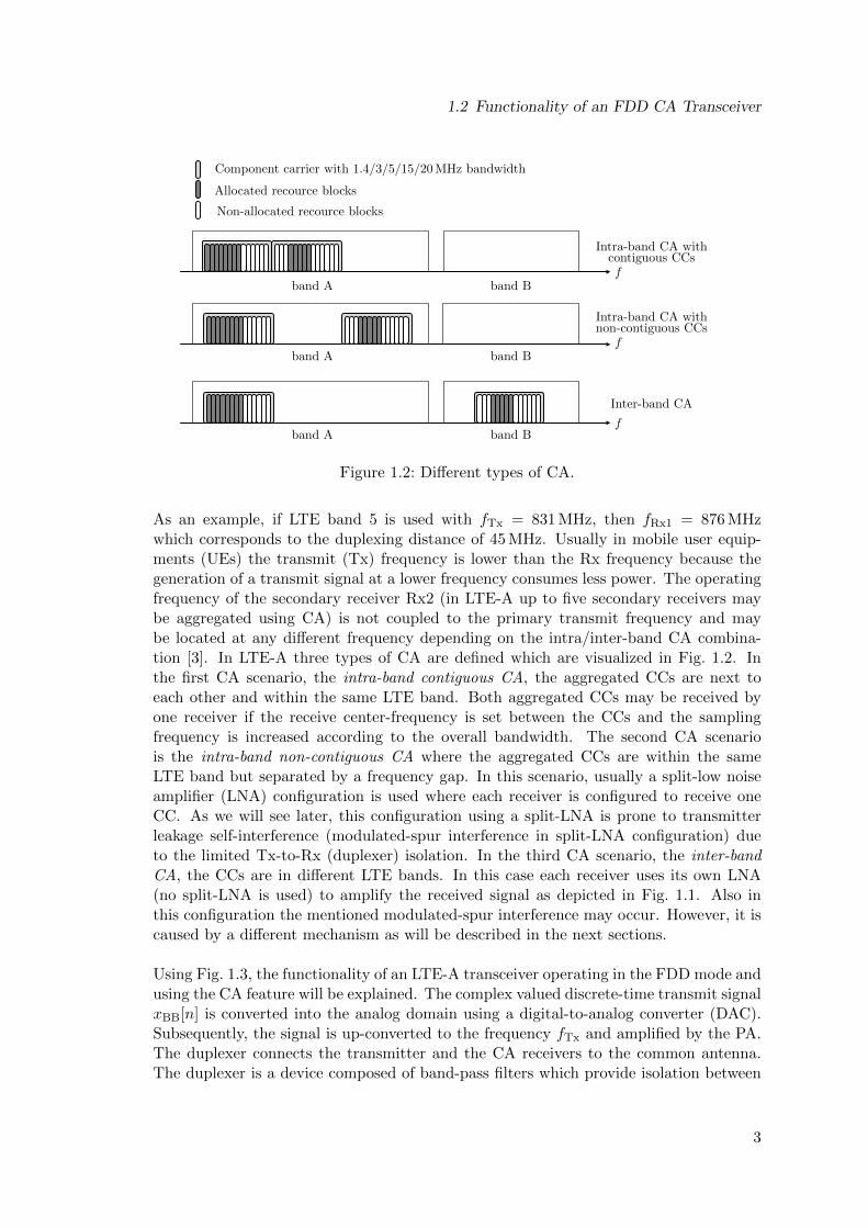
Using Fig. 1.3, the functionality of an LTE-A transceiver operating in the FDD mode andusing the CA feature will be explained. The complex valued discrete-time transmit signalxBB[n] is converted into the analog domain using a digital-to-analog converter (DAC).Subsequently, the signal is up-converted to the frequency fTx and amplified by the PA.The duplexer connects the transmitter and the CA receivers to the common antenna.The duplexer is a device composed of band-pass filters which provide isolation between
3
1 Introduction
xBB[n]
Rx2
Rx1
Tx
yTotBB[n]
A
D
A
D
A
D
f
f
f
f f
f0
0fRx2
fRx1
fRx2
hs[n]
hs[n]
CSF
CSF
LNA
LNA
fTx
yRxRF(t)
PA
fTx
fRx1
fTx
fTx
xRF(t)
Tx leakage
duplexing distance
Figure 1.3: The transmitter leakage signal into the own receivers.
the Tx and Rx paths. Thereby, the duplexer passes the transmit signal to the antennawhere it is radiated to the base-station. At the same time signals at the frequenciesfRx1 and fRx2 are received by the antenna and fed by the duplexer to the correspondingreceivers. RF switches are used to select the appropriate duplexer depending on thefrequency band. The received signals are amplified by the LNAs, and assuming direct-conversion receivers, the wanted receive signals are down-converted to the BB. This BBsignals are then digitized by the analog-to-digital converters (ADCs), and filtered by thechannel-select filters (CSFs). As indicated in Fig. 1.1, the DFE provides the connectionto the digital BB where the received data streams are demodulated, and the Tx data ismodulated for the transmission, respectively.
1.3 Transmitter Leakage Induced Self-Interferences
Due to the limited duplexer isolation between the transmitter and the receivers whichis in the range of 50 dB to 55 dB [4, 5], a transmitter leakage (TxL) signal occurs in thereceivers which may be stronger than the actual receive signal. Assuming a transmitterpower of 23 dBm at the antenna1, and an average Tx-to-Rx duplexer isolation of 50 dBaround the transmit frequency, the TxL signal power at the input of the receiver isPTxL
RF = 23 dBm− 50 dB = −27 dBm. On the other hand, in so called reference sensitiv-ity cases (where the mobile equipment is far away from the base-station), the wantedsignal power at the antenna can be as low as -97 dBm [3], which is 70 dB below the TxLsignal power. In an ideal transceiver this would not be an issue due to the fact that
1At the PA output the Tx power may be even higher due to the switch-, and duplexer insertion losses.
4
1.3 Transmitter Leakage Induced Self-Interferences
the signals are located at different frequencies. However, because of non-idealities in theanalog front-end this TxL signal can create a BB interference which disturbs the wantedreceive signal significantly.
The TxL signal is the root cause of several receiver interferences which degrade the re-ceiver performance. The actual type of receiver interference depends on the transceiveroperating conditions, e.g., enabled Rx/Tx CA. The following section gives an overviewabout the different types of interferences. A detailed explanation of each interferencefollows in Section 2.1.
Non-CA related Interferences:
Second-Order Intermodulation Distortion (IMD2) InterferenceThe leaking transmitter signal may cause a second-order intermodulation distor-tion (IMD2) interference in direct-conversion receivers [6], [7]. This second-ordernonlinear distortion always falls around zero-frequency and is caused by e.g. acoupling between the RF- and local oscillator (LO)-ports in the in-phase (I)-, andquadrature-phase (Q)-path of the Rx IQ-mixer [8].
Tx Noise in Rx BandThe TxL signal may have a spectral emission (skirt) due to the nonlinearity of thePA which may reach up to the Rx frequency range. As a consequence, this Txnoise spectral content may overlay the wanted receive signal leading to a receivesignal degradation.
Reciprocal MixingReciprocal mixing means that a blocker2 signal (e.g. the TxL signal) is down-converted into the BB due to the LO phase noise (PN) where it degrades thewanted signal quality.
Receiver CA related interferences:
Continuous-Wave SpurContinuous-Wave Spurs may be generated by device nonlinearities and couplingbetween the receive mixer harmonics of the square-wave mixers. Such a continuouswave (CW)-spur (cosine-like signal) may be down-converted by the Rx mixer andmay occur as spectral peak in the receive spectrum.
Modulated Spur Interference in Inter-Band CADue to multiple clock sources, which are needed to cover the different CA scenariosand band combinations, cross-talk between the LO lines of the receivers on the chiptogether with device nonlinearities may create spurs in the receiver front-end. Ifthe frequency of such a spur falls near the actual Tx frequency, the TxL signal maybe down-converted into the Rx BB. This so called modulated spur interferencecan disturb the wanted receive signal significantly [9, 10].
2A blocker signal is an unwanted signal at the input of the receiver which is either received by theantenna or created by the own transmitter leakage.
5
1 Introduction
Modulated Spur Interference in Intra-Band CA with Split-LNAIn intra-band CA where a split-LNA is used, the TxL signal may be mixed by theharmonics of the mixer in the first CA receiver. This mixed TxL signal is reflectedback to the input of the split-LNA where it reaches the input of the secondaryreceiver. The harmonics of the mixer in the secondary receiver may down-convertthe reflected signal to the BB where it disturbs the wanted signal.
Tx Harmonics in DownlinkThe potentially leaking transmitter harmonic distortions caused by the nonlinearPA may overlap the wanted receive signal of the secondary CA receiver which isnot coupled to the primary transmit frequency [11].
Tx Harmonics in Downlink Harmonic ResponseDue to the square-wave mixer implementation in the receiver, leaking transmitterharmonic distortions caused by the nonlinearity in the transmitter may be down-converted to the BB by the harmonics of the mixer.
Transmitter CA related Interferences:
Multiple Modulated SpursEach transmitter causes its own TxL signal which may cause multiple modulatedspurs.
Multiple Tx Harmonics in Downlink/Downlink Harmonic ResponseThe harmonics of each transmitter may fall on top of the wanted Rx signal or maybe down-converted into the BB by the mixer harmonics.
Intermodulation DistortionsWhen several transmitters are operated in parallel, each transmitter may createan IMD2 interference in the receiver(s). If the transmit signal is either created inan intra-band non-contiguous CA, or an inter-band CA scenario, nonlinearities inthe analog front-end may create a third-order intermodulation distortion (IMD3)which interferes with the wanted receive signal.
The severity of the TxL signal caused interferences could be reduced by increasing theduplexer isolation. However, besides the increasing costs, improving the Tx-to-Rx isola-tion of the duplexer would lead to a higher insertion loss of the wanted receive signal andthereby to a reduction of the Rx signal quality. Therefore, instead of using improved du-plexers, efficient ways to cancel the transmitter induced self-interferences are of specialinterest.
1.4 State of the Art
In the existing literature several approaches are discussed to mitigate the TxL signaland PA spurious emission caused receiver desensitization. A natural approach wouldbe to cancel the transmitter leakage signal in the RF domain before it enters the in-put of the LNA or mixer. This would significantly reduce the generation of nonlineardistortions due to receiver RF front-end nonlinearities. The authors in [12] propose anRF cancellation architecture using an auxiliary transmitter to generate a Tx leakage
6

1.4 State of the Art
signal replica (including nonlinear PA distortions) in the RF domain which is subtractedfrom the received signal before it enters the LNA. The replica signal is generated byan nonlinear adaptive decorrelation-based learning algorithm which uses the known Txsamples and the received signal in the digital BB. With this approach, the authors areable to increase the effective Tx-to-Rx isolation by 54 dB.
A different way to suppress the leakage signal may be achieved by using N-path fil-ters which act as a notch filter at the transmit frequency. In [5, 13] and [14], suchN-path filters are placed in front of the mixer input to reject the TxL signal.
To limit the computational complexity of a pure digital modulated spur interferencecancellation, the authors in [15] use an auxiliary receiver to sense the TxL signal at thereceiver input which is subsequently used as a reference signal for a digital cancellationalgorithm. With this mixed-signal approach, the auxiliary receiver senses the Tx signalincluding nearby out-of-band (OOB) emissions after it passed the duplexer Tx-to-Rxstop-band. This means, the duplexer stop-band frequency response including the TxOOB emissions are already included in the sensed TxL signal and do not need to beestimated by the digital algorithm. This heavily reduces the complexity of the digitalpart of the cancellation approach. The same auxiliary receiver could also be used tosense spurious emissions of the transmitter which desensitize the receiver. However,nonlinearities of the receiver are not covered and need to be estimated by the digitalcancellation algorithm. Using an auxiliary receiver with a serial-mixing concept to can-cel the modulated spur interference [9], [10] including the PN of the involved transmitterand receiver LOs is presented in [16].
An IMD2 interference in the receiver may also be generated by external blocker sig-nals received by the antenna. The author in [17, 18], extracts the blocker signal afterthe Rx mixer by a high-pass filter. The squared envelope of this signal is then used as areference for the subsequent adaptive filter which cancels the generated IMD2 interfer-ence.
Although, analog and mixed signal cancellation techniques offer good cancellation resultsas stated in [12], [15], [16], their additional hardware effort is not negligible. Especiallyin CA, where multiple receiver chains are operated in parallel, each receiver (possiblyincluding the diversity receivers) requires its own auxiliary transmitter (RF cancella-tion)/receiver (mixed signal cancellation) because of the different duplexer stop-bandresponses seen from the Tx to each receiver. A big challenge in designing analog ormixed-signal cancellation circuits is to limit the degradation of the wanted receive signalby connecting the auxiliary receiver [15], or transmitter [12] to the main receiver. Besidethis, pure digital approaches offer technology independence and scalability and do notneed any changes of the analog front-end circuit. However, the computational burdenin the digital BB is increased.
Several fully digital techniques to cancel Tx-induced self-interferences can be found inthe existing literature. The authors in [19] present the modeling and digital mitigationof transmitter self-interference in the presence of transmitter and receiver nonlinearities.In [20], the digital suppression of the nonlinear PA OOB emission (Tx noise in Rx band)
7
1 Introduction
which reaches up to the Rx band in case of low duplexing distances is presented. Thenonlinearity of the PA induces also spurious distortions (Tx harmonics) which may de-grade one of the CA receivers. The digital cancellation of such distortions in the presenceof transmitter IQ-imbalance is suggested in [11].
There is also existing literature for the pure digital cancellation of the transmitter in-duced IMD2 interference in direct-conversion receivers. In [21] a frequency flat duplexerstop-band in the region of the leaked Tx signal is assumed. The IMD2 interference is es-timated adaptively by a least-mean-squares (LMS) filter where only the coefficient withlargest magnitude is used for the cancellation. Similar assumptions are made in [22].However, the assumption of a frequency-flat duplexer response is not valid for LTE-Asignals due to the wider bandwidth. In [23] a Volterra kernel based least-squares (LS)approach for frequency-selective duplexers is introduced. The CSF in the receiver isequalized to obtain the unfiltered IMD2 interference with twice the Tx signal bandwidthfor the IMD2 LS estimation. Finally the authors in [6] present a compensation of theIMD2 interference in the presence of a static 3rd-order PA nonlinearity and Tx mixerIQ-imbalance. The estimation process consists of a two-step LS approach which has ahigh computational complexity. Further, [21] and [22] are assuming equal IMD2 inter-ferences in the I- and Q-branch of the Rx mixer, whereas in [23] they are assumed to bedifferent.
1.5 Scope of this Work
Although, the existing literature provides solutions for pure digital cancellation of TxLsignal caused receiver interferences, the computational complexity of most solutions isfar too high to be implemented in a real mobile transceiver. Additionally, no literatureregarding the pure digital cancellation of the modulated spur interference was availableat the time when this PhD work has started. The goal of this thesis is the developmentof specialized low-complexity adaptive filter algorithms which could be implemented intoday’s transceivers. Motivated by this, and by using the detailed interference modelswhich are derived in this thesis, low-complexity adaptive algorithms for a pure digitalcancellation of the modulated spur-, and the IMD2 interference are proposed.
This thesis resulted in the following achievements:
The derivation of a detailed baseband equivalent model of the modulated-spur-,Tx-harmonics-, IMD2-, and third-order nonlinear interferences.
The development of a normalized widely-linear variable step-size LMS adaptivefilter to cancel the main and image modulated spur interference in the digital BBof the CA transceiver.
The development of a low-complexity nonlinear LMS-type adaptive filter to cancelthe IMD2 interference generated by a Tx signal which traveled through a highlyfrequency-selective Tx-to-Rx leakage path.
The development of a robust nonlinear recursive-least-squares (RLS)-type adaptivefilter for the IMD2 cancellation which is suitable for highly frequency-selectiveduplexer stop-band responses and clustered-transmit signals.
8
1.5 Scope of this Work
The development of a harmonic rejection (HR) mixer concept to suppress specificharmonics in 25% duty-cycle mixers. With this approach, the down-conversion ofblocker signals by the harmonics of the mixer can be suppressed.
During the work on this thesis the following scientific contributions have been publishedin peer reviewed conference proceedings and journals or have been filed as patents. Someideas and figures presented in this thesis previously appeared in these publications andpatents:
Journal Publications
A. Gebhard, O. Lang, M. Lunglmayr, C. Motz, R. S. Kanumalli, C. Auer, T.Paireder, M. Wagner, H. Pretl and M. Huemer, ”A Robust Nonlinear RLS TypeAdaptive Filter for Second-Order-Intermodulation Distortion Cancellation in FDDLTE and 5G Direct Conversion Transceivers,” In IEEE Transactions on MicrowaveTheory and Techniques, 16 pages, Early Access, January 2019.
S. Sadjina, R. S. Kanumalli, A. Gebhard, K. Dufrene, M. Huemer and H. Pretl,”A Mixed-Signal Circuit Technique for Cancellation of Interferers Modulated byLO Phase-Noise in 4G/5G CA Transceivers,” In IEEE Transactions on Circuitsand Systems – I Regular Papers, Vol. 65, No. 11, pp. 3745-3755, Nov 2018.
R. S. Kanumalli, T. Buckel, C. Preissl, P. Preyler, A. Gebhard, C. Motz, J.Markovic, D. Hamidovic, E. Hager, H. Pretl, A. Springer and M. Huemer, ”Digitally-intensive Transceivers for Future Mobile Communications - Emerging Trends andChallenges,” In e&i Elektrotechnik und Informationstechnik, Vol. 135, No. 1, pp.30-39, January 2018.
Conference Publications
A. Gebhard and C. Motz and R. S. Kanumalli and H. Pretl and M. Huemer, ”Non-linear Least-Mean-Squares Type Algorithm for Second-Order Interference Can-cellation in LTE-A RF Transceivers,” In Proceedings of the 51st IEEE AsilomarConference on Signals, Systems, and Computers, Oct 2017, pp. 802-807.
A. Gebhard, M. Lunglmayr and M. Huemer, ”Investigations on Sparse SystemIdentification with l0-LMS, Zero-Attracting LMS and Linearized Bregman Itera-tions,” In Proceedings of the 16th International Conference on Computer AidedSystem Theory - EUROCAST, February 2018.
A. Gebhard and R. S. Kanumalli and B. Neurauter and M. Huemer, ”Adaptive Self-Interference Cancellation in LTE-A Carrier Aggregation FDD Direct-ConversionTransceivers,” In Proceedings of the IEEE Sensor Array and Multichannel SignalProcessing Workshop (SAM 2016), July 2016, 5 pages.
R. S. Kanumalli, A. Gebhard, A. Elmaghraby, A. Mayer, D. Schwartz and M.Huemer, ”Active Digital Cancellation of Transmitter Induced Modulated SpurInterference in 4G LTE Carrier Aggregation Transceivers,” In Proceedings of the83rd IEEE Vehicular Technology Conference (VTC Spring), May 2016, 5 pages.
9
1 Introduction
Scientific Talks
A. Gebhard, ”All Digital Interference Cancellation Architectures for RF Trans-ceivers,” Evaluation of the Christian Doppler Laboratory for Digitally Assisted RFTransceivers for Future Mobile Communications, Johannes Kepler University, Linz,Austria, November 2018.
A. Gebhard, ”Investigations on Sparse System Identification with l0-LMS, Zero-Attracting LMS and Linearized Bregman Iterations”, International Conference onComputer Aided Systems Theory (EUROCAST 2017), Las Palmas, Gran Canaria,February 2017.
A. Gebhard, ”Adaptive Self-Interference Cancelation in LTE-A Carrier Aggre-gation FDD Direct-Conversion Transceivers”, 62. Fachgruppentreffen der ITGFachgruppe ”Algorithmen fur die Signalverarbeitung”, Johannes Kepler University,Linz, Austria, October 2016.
A. Gebhard, ”Adaptive Self-Interference Cancelation in LTE-A Carrier Aggrega-tion FDD Direct-Conversion Transceivers”, IEEE Sensor Array and MultichannelSignal Processing Workshop (SAM 2016), Rio de Janeiro, Brazil, July 2016.
A. Gebhard, ”Self-Interference Cancellation in LTE Carrier Aggregation Trans-ceivers” PhD-Day at DMCE/Intel Austria, Linz, Austria, May 2016.
Poster Presentations
A. Gebhard, ”Nonlinear Least-Mean-Squares Type Algorithm for Second-OrderInterference Cancellation in LTE-A RF Transceivers”, ASILOMAR Conference onSignals, Systems, and Computers, Pacific Grove, USA, October 2017.
A. Gebhard, ”Modulated Spurs in LTE-A Carrier Aggregation Transceivers”, Mi-croelectronic Systems Symposium (MESS16), Vienna, Austria, April 2016.
Patents / Patent Applications
A. Gebhard, S. Sadjina, K. Dufrene and S. Tertinek, ”Harmonic Suppressing Lo-cal Oscillator Signal Generation,” U.S. Patent US 9,935,722 B2, filed June 2016,granted April 2018.
S. Tertinek, A. Gebhard, S. Sadjina and K. Dufrene, ”Pulse Generation UsingDigital-to-Time Converter,” U.S. Patent US 9,755,872 B1, filed August 2016,granted September 2017.
K. Dufrene, Ram S. Kanumalli, S. Sadjina and A. Gebhard, ”Multiple ModulatedSpur Cancellation Apparatus,” U.S. Patent Application US 2017/0359136 A1, filedJune 2016, published December 2017.
A. Gebhard, ”Second Order Intermodulation Cancellation for RF Transceivers,”U.S. Patent US 10,172,143 B2, filed June 2017, granted January 2019.
K. Dufrene, S. Sadjina, A. Gebhard and Ram S. Kanumalli, ”Interference De-tection Device, Interference Detection Apparatus, Interference Detection Method,Computer Program, Receiver, Mobile Terminal and Base Station,” U.S. Patent US10,097,220 B2, filed May 2017, granted October 2018.
10
1.5 Scope of this Work
The outline of the work presented in this thesis is:
Chapter 2 gives a detailed explanation of the most important TxL signal caused receiverself-interferences. Here, two mechanisms are explained which lead to the modulatedspur interference. The first mechanism is caused by LO-to-LO crosstalk in inter-bandCA scenarios, and the second mechanism occurs in intra-band CA where a split-LNA isused. Furthermore, baseband equivalent models for the modulated spur-, Tx harmonics-,IMD2-, and the third-order nonlinear interferences are derived considering nonlinearitiesin the transmitter- and in the receiver path. Finally, BB equivalent models for highereven-order intermodulation distortions which are caused by a combination of the LNA-,and the mixer nonlinearity are deduced.
In Chapter 3, the HR mixer concept is explained and a novel HR concept for 25% duty-cylce current-driven passive mixers is proposed. The rejection of a specific harmoniccontent of the Rx square-wave mixers is used to suppress specific receiver interferenceslike the modulated spur-, or the Tx harmonics interference.
In Chapter 4, linear adaptive filters like the complex-valued LMS-, and RLS algorithmare recapitulated using the Wirtinger Calculus [24]. These algorithms are subsequentlyused to demonstrate the digital cancellation of the modulated spur interference. Theresults and key findings of this chapter have been published in [9, 16].
Chapter 5 starts with an introduction of nonlinear adaptive filtering in the context of thepure digital IMD2 interference cancellation. Polynomial filters [25, 26] like the Volterrakernel based filter are investigated for the IMD2 cancellation. Subsequently, a novelWiener-model based nonlinear LMS-type algorithm (IM2LMS), and a novel nonlinearRLS-type algorithm (IM2RLS) are proposed to cancel the IMD2 interference in the dig-ital BB. The suggested IMD2 cancellation algorithms are evaluated using simulated andmeasured IMD2 data. The measured IMD2 data is obtained from two different mea-surement setups. The first setup includes a transceiver chip provided by the industrialpartner, whereas the second setup uses discrete RF components. The derivation and theperformance results of the IM2LMS-, and IM2RLS algorithms have been presented in[7] and [27], respectively.
Finally, Chapter 6 concludes the work and gives an outlook on potential future researchtopics in this field.
11

2Interferences in FDD RF Transceivers
2.1 Interference Overview
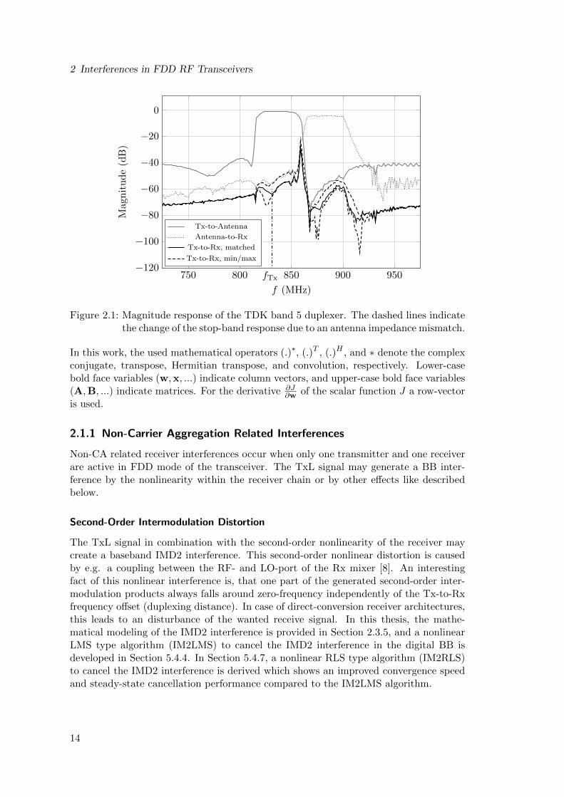
One of the main reasons of receiver desensitization in FDD transceivers is the lim-ited duplexer isolation between the transmitter(s) and the receiver(s) which is around50 dB to 55 dB [4, 5]. The resulting TxL signal into the receivers in combination withfront-end non-idealities may generate BB interferences which degrade the receiver per-formance. The Tx-to-Rx stop-band isolation versus frequency obtained by a 4-pole S-parameter measurement of a commercial band 5 duplexer [28] is depicted in Fig. 2.1. Thedashed lines indicate the change of the Tx-to-Rx isolation caused by a variation of theantenna impedance mismatch corresponding to a maximally allowed voltage-standing-wave-ratio (VSWR) of 2 [28]1. It can be observed, that the resulting TxL signal intothe receiver experiences a frequency-selective behavior of the duplexer in the stop-band.This TxL signal can be identified as the root cause of several receiver BB interferences.
In this chapter the TxL signal caused receiver interferences are modeled in the RFdomain, and the resulting BB equivalent receiver interferences are determined. Thisincludes the modeling of the modulated spur-, Tx harmonics-, IMD2-, and higher even-order intermodulation interferences. The down-conversion of the TxL signal by spurscreates the modulated spur interference which may consist of a main and an image com-ponent. This spurs may be generated through cross-talk between the LO lines of thereceivers on the chip together with device nonlinearities. The modulated spur interfer-ence may also be generated by the use of split-LNAs in intra-band CA scenarios. Thesecond-order nonlinearity of the mixer creates an IMD2 interference which always fallsaround the zero-frequency. In case of direct-conversion receiver architectures, this leadsto a BB interference which disturbs the wanted receive signal. Furthermore, the 25%duty-cycle current driven passive mixer [29] which is preferably used in direct-conversionreceivers is modeled. Due to the square-wave control signals, harmonics are producedwithin the mixer which may lead to the down-conversion of unwanted spectral compo-nents into the receiver BB. This down-conversion by the harmonic response of the mixermay degrade the receiver performance.The receiver interferences can be split into interferences which occur in a single Tx/RxFDD transceiver, and in Tx/Rx CA related interferences. The next sections will explainthe different TxL signal caused receiver interferences, and for each interference methodsfor the prevention are discussed briefly.
1A VSWR of 2 corresponds to a reflection coefficient with magnitude 0.333. To obtain the dashed linesin Fig. 2.1 the angle of the complex valued reflection coefficient is varied between 0 and 360 andthe min./max. value is plotted.
13
2 Interferences in FDD RF Transceivers
750 800 850 900 950−120
−100
−80
−60
−40
−20
0
f (MHz)
Mag
nit
ud
e(d
B)
Tx-to-Antenna
Antenna-to-Rx
Tx-to-Rx, matched
Tx-to-Rx, min/max
fTx
Figure 2.1: Magnitude response of the TDK band 5 duplexer. The dashed lines indicatethe change of the stop-band response due to an antenna impedance mismatch.
In this work, the used mathematical operators (.)∗, (.)T , (.)H , and ∗ denote the complexconjugate, transpose, Hermitian transpose, and convolution, respectively. Lower-casebold face variables (w,x, ...) indicate column vectors, and upper-case bold face variables(A,B, ...) indicate matrices. For the derivative ∂J
∂w of the scalar function J a row-vectoris used.
2.1.1 Non-Carrier Aggregation Related Interferences
Non-CA related receiver interferences occur when only one transmitter and one receiverare active in FDD mode of the transceiver. The TxL signal may generate a BB inter-ference by the nonlinearity within the receiver chain or by other effects like describedbelow.
Second-Order Intermodulation Distortion
The TxL signal in combination with the second-order nonlinearity of the receiver maycreate a baseband IMD2 interference. This second-order nonlinear distortion is causedby e.g. a coupling between the RF- and LO-port of the Rx mixer [8]. An interestingfact of this nonlinear interference is, that one part of the generated second-order inter-modulation products always falls around zero-frequency independently of the Tx-to-Rxfrequency offset (duplexing distance). In case of direct-conversion receiver architectures,this leads to an disturbance of the wanted receive signal. In this thesis, the mathe-matical modeling of the IMD2 interference is provided in Section 2.3.5, and a nonlinearLMS type algorithm (IM2LMS) to cancel the IMD2 interference in the digital BB isdeveloped in Section 5.4.4. In Section 5.4.7, a nonlinear RLS type algorithm (IM2RLS)to cancel the IMD2 interference is derived which shows an improved convergence speedand steady-state cancellation performance compared to the IM2LMS algorithm.
14
2.1 Interference Overview
Prevention/mitigation methods:The IMD2 interference may be minimized by using duplexers with higher Tx-to-Rx iso-lation to attenuate the TxL signal. However, this leads to higher costs for the duplexersand increased insertion losses. In this thesis, the IMD2 cancellation by adaptive sig-nal processing techniques is suggested. The IM2LMS, and the IM2RLS algorithm areproposed for this purpose.
Tx Noise in the Rx Band
The overall nonlinearity of the transmitter (including the nonlinear PA) which mayinclude a memory effect generates a spectral skirt around the Tx signal bandwidthwhich reaches up to the Rx frequency range. The residual skirt content after passingthrough the duplexer Tx-to-Rx stop-band together with the wanted receive signal isdown-converted by the receiver LO. This may lead to a receiver desensitization whenthe transceiver is operating in LTE bands with small duplexing distance. E.g. as de-scribed in [20, 30], for Tx intra-band CA scenarios, the duplexing distance can be assmall as 15 MHz.
Prevention/mitigation methods:The nonlinearity of the transmitter can be reduced by using a pre-distortion of the trans-mit signal. Another possibility to limit the OOB emission at the Rx band would be theuse of duplexers with higher isolation which generates additional costs.
Reciprocal Mixing
The Rx mixer is down-converting the wanted Rx signal to the BB. Similarly, also theTxL signal is down-converted by the mixer resulting in a strong blocker signal at theduplexing distance. Due to the LO PN, the spectral content of the down-convertedTxL blocker signal may reach the wanted signal frequency range. This effect is calledreciprocal mixing, where the spectral skirt caused by the down-conversion of the blockerdue to the LO PN disturbs the wanted signal. The cancellation of the reciprocal mixinginterference using an auxiliary receiver is presented in [31]. As the PN of the LO israndom, a pure digital cancellation is not feasible.
Prevention/mitigation methods:The reciprocal down-conversion of the TxL signal may be mitigated by using duplexerswith higher Tx-to-Rx isolation or employing LOs with high spectral purity.
2.1.2 Rx Carrier Aggregation Related Interference Problems
Continuous-Wave Spurs
Due to the square-wave mixer implementation, harmonics of the different LO frequen-cies are generated which may couple over the LO lines on the chip. If additional devicenonlinearities are present, new spur frequencies may occur through the nonlinear mixingprocess. The resulting CW spurs may either overly the wanted Rx signal, or directly fallinto the BB. Also other clock sources on the RF-transceiver chip like the ADC or thedigitally controlled oscillator (DCO) may lead to spurs. If such a CW spur is present in
15
2 Interferences in FDD RF Transceivers
︷ ︸︸ ︷
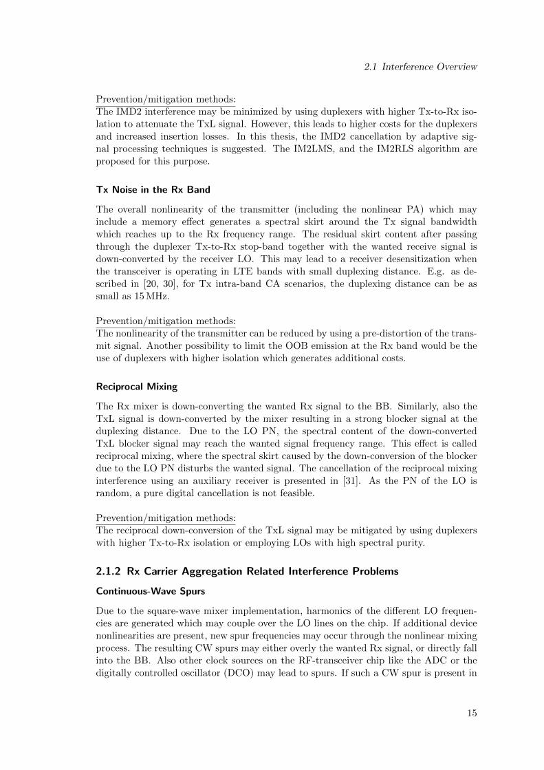
fsp = 6fRx1 − 6fRx2 = 828 MHz
738 MHz 831 MHz 876 MHz
band 12 DL729-746 MHz
band 5 UL824-849 MHz
band 5 DL869-894 MHz
4428 MHz 5256 MHz
fRx2 fTx fRx1 6fRx2 6fRx1
f
Figure 2.2: Device nonlinearities and the mixer harmonics on the transceiver chip leadto a spur which is 3 MHz below the transmit frequency fTx.
the Rx baseband it occurs there as spectral peak which disturbs the wanted signal.
Prevention/mitigation methods:In the transceiver layout, oscillators are placed on the chip die with largest possible dis-tance between them. This minimizes coupling effects. Decoupling of the supplies withlarge shunt capacitors may reduce the supply-crosstalk related spurs. From a signalprocessing point of view, a CW spur falling into the Rx BB may be mitigated by usingdigital interference cancellation in the BB e.g. by using a single tap LMS algorithm.
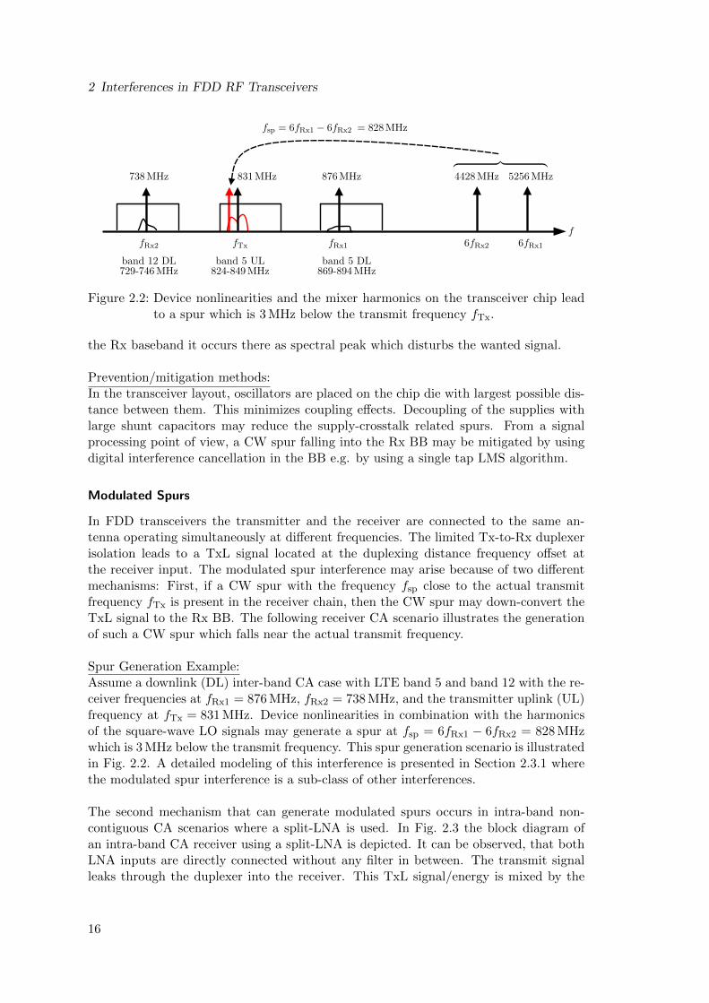
Modulated Spurs
In FDD transceivers the transmitter and the receiver are connected to the same an-tenna operating simultaneously at different frequencies. The limited Tx-to-Rx duplexerisolation leads to a TxL signal located at the duplexing distance frequency offset atthe receiver input. The modulated spur interference may arise because of two differentmechanisms: First, if a CW spur with the frequency fsp close to the actual transmitfrequency fTx is present in the receiver chain, then the CW spur may down-convert theTxL signal to the Rx BB. The following receiver CA scenario illustrates the generationof such a CW spur which falls near the actual transmit frequency.
Spur Generation Example:Assume a downlink (DL) inter-band CA case with LTE band 5 and band 12 with the re-ceiver frequencies at fRx1 = 876 MHz, fRx2 = 738 MHz, and the transmitter uplink (UL)frequency at fTx = 831 MHz. Device nonlinearities in combination with the harmonicsof the square-wave LO signals may generate a spur at fsp = 6fRx1 − 6fRx2 = 828 MHzwhich is 3 MHz below the transmit frequency. This spur generation scenario is illustratedin Fig. 2.2. A detailed modeling of this interference is presented in Section 2.3.1 wherethe modulated spur interference is a sub-class of other interferences.
The second mechanism that can generate modulated spurs occurs in intra-band non-contiguous CA scenarios where a split-LNA is used. In Fig. 2.3 the block diagram ofan intra-band CA receiver using a split-LNA is depicted. It can be observed, that bothLNA inputs are directly connected without any filter in between. The transmit signalleaks through the duplexer into the receiver. This TxL signal/energy is mixed by the
16
2.1 Interference Overview
LNA
LNA
PA
CSF
CSFA
D
A
D
A
D
Tx leakage
fTx
fTx
fTx
fTx
fRx2 fRx2
fRx1
Rx2
Rx1
Tx
Figure 2.3: Modulated spur interference occuring in intra-band non-contiguous CA sce-narios using a split-LNA.
harmonics of the mixer Rx1 and reflected back to the split-LNA input. This reflectedenergy/signal reaches the input of the secondary LNA because of the lack of reverse iso-lation of the LNAs. The Rx2 mixer is down-converting this reflected energy by anothermixer harmonic down to the BB.
A detailed modeling of the modulated spur interference in split-LNA configuration ispresented in Section 2.5. Interestingly, both mechanisms are leading to the same BBmodulated spur interference which disturbs the wanted Rx signal. In [10, 9] the authorof this thesis gives a detailed description of the modulated spur cancellation in FDD RFtransceivers by adaptive filtering.
Prevention/mitigation methods:As the generation of CW spurs cannot be prevented only by layout techniques, a highduplexer isolation is needed to suppress the TxL signal. This increases the costs of theduplexers and has the undesirable side effect of increased insertion loss, too. Split-LNArelated modulated spurs may be prevented by increasing the reverse isolation of theLNA. Consequently, no signal energy is reflected to the other split-LNA. Another pos-sibility is the use of HR mixers to suppress the harmful harmonics of the square-wavemixers. The contributions [9, 10, 16] published by the author of this thesis provide amathematical model and the digital cancellation of the modulated-spur interference.
17
2 Interferences in FDD RF Transceivers
Tx Harmonics in Downlink
In DL CA, the primary Rx (Rx1) LO frequency is always coupled via the duplexingdistance to the primary Tx (Tx1) frequency. But the secondary Rx (Rx2) LO fre-quency is not coupled to the primary Tx frequency and may be located at any differentfrequency depending on the intra/inter-band CA combination. When one of the har-monics of Tx1 (e.g. 2nd, 3rd or 5th) which are produced by the nonlinearity of thetransmitter (including Tx switches) is close to the Rx2 LO frequency, then the Tx har-monic is directly down-converted to the BB. Example: fTx = 700 MHz (low band) andfRx2 ≈ 3fTx = 2100 MHz (high band).
Prevention/mitigation:The linearization of the PA using pre-distortion of the transmit signal may reduce thegeneration of Tx harmonics. A high duplexer isolation suppresses the leaking Tx har-monics but leads to higher costs and insertion losses. The mathematical model which isprovided in Section 2.3.1 indicates, that the Tx harmonics interference may be efficientlycanceled by adaptive signal processing techniques.
Tx Harmonics in the Downlink Harmonic Response
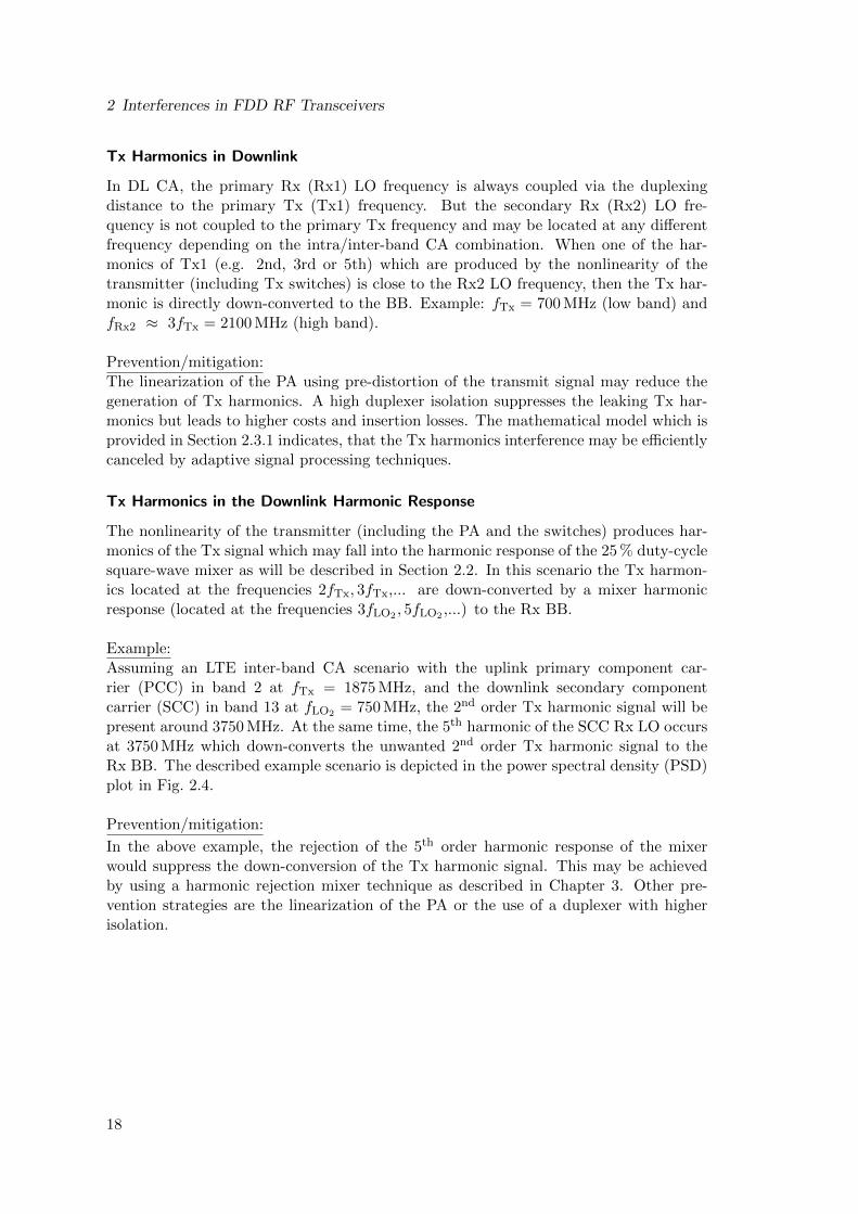
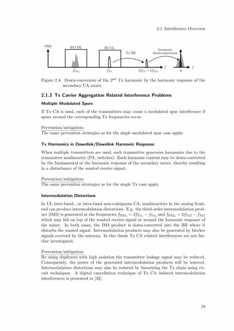
The nonlinearity of the transmitter (including the PA and the switches) produces har-monics of the Tx signal which may fall into the harmonic response of the 25 % duty-cyclesquare-wave mixer as will be described in Section 2.2. In this scenario the Tx harmon-ics located at the frequencies 2fTx, 3fTx,... are down-converted by a mixer harmonicresponse (located at the frequencies 3fLO2 , 5fLO2 ,...) to the Rx BB.
Example:Assuming an LTE inter-band CA scenario with the uplink primary component car-rier (PCC) in band 2 at fTx = 1875 MHz, and the downlink secondary componentcarrier (SCC) in band 13 at fLO2 = 750 MHz, the 2nd order Tx harmonic signal will bepresent around 3750 MHz. At the same time, the 5th harmonic of the SCC Rx LO occursat 3750 MHz which down-converts the unwanted 2nd order Tx harmonic signal to theRx BB. The described example scenario is depicted in the power spectral density (PSD)plot in Fig. 2.4.
Prevention/mitigation:
In the above example, the rejection of the 5th order harmonic response of the mixerwould suppress the down-conversion of the Tx harmonic signal. This may be achievedby using a harmonic rejection mixer technique as described in Chapter 3. Other pre-vention strategies are the linearization of the PA or the use of a duplexer with higherisolation.
18
2.1 Interference Overview
PSD B13 DL
fLO2
B2 UL
fTx 2fTx = 5fLO2
Tx H2harmonic
down-conversion
f f0
Figure 2.4: Down-conversion of the 2nd Tx harmonic by the harmonic response of thesecondary CA mixer.
2.1.3 Tx Carrier Aggregation Related Interference Problems
Multiple Modulated Spurs
If Tx CA is used, each of the transmitters may cause a modulated spur interference ifspurs around the corresponding Tx frequencies occur.
Prevention/mitigation:The same prevention strategies as for the single modulated spur case apply.
Tx Harmonics in Downlink/Downlink Harmonic Response
When multiple transmitters are used, each transmitter generates harmonics due to thetransmitter nonlinearity (PA, switches). Each harmonic content may be down-convertedby the fundamental or the harmonic response of the secondary mixer, thereby resultingin a disturbance of the wanted receive signal.
Prevention/mitigation:The same prevention strategies as for the single Tx case apply.
Intermodulation Distortions
In UL inter-band-, or intra-band non-contiguous CA, nonlinearities in the analog front-end can produce intermodulation distortions. E.g. the third-order intermodulation prod-uct (IM3) is generated at the frequencies fIM31 = 2fTx1 − fTx2 and fIM32 = 2fTx2 − fTx1
which may fall on top of the wanted receive signal or around the harmonic response ofthe mixer. In both cases, the IM3 product is down-converted into the BB where itdisturbs the wanted signal. Intermodulation products may also be generated by blockersignals received by the antenna. In this thesis Tx CA related interferences are not fur-ther investigated.
Prevention/mitigation:By using duplexers with high isolation the transmitter leakage signal may be reduced.Consequently, the power of the generated intermodulation products will be lowered.Intermodulation distortions may also be reduced by linearizing the Tx chain using cir-cuit techniques. A digital cancellation technique of Tx CA induced intermodulationinterferences is presented in [32].
19
2 Interferences in FDD RF Transceivers
2.2 Operation of the 25% Duty-Cycle Current-Driven PassiveMixer
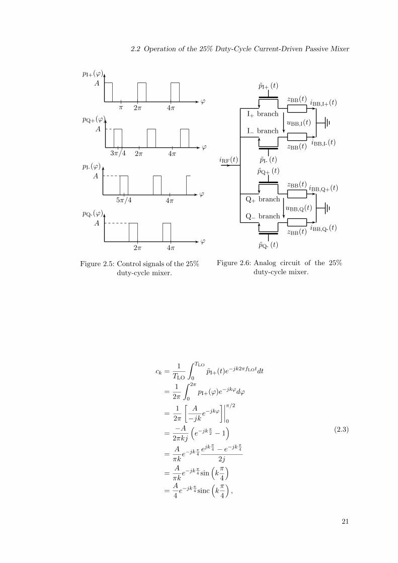
Mixers are used to shift the desired RF signal to the baseband or an intermediate-frequency where the wanted signal is digitized for further digital signal processing. Fre-quency translation may be realized by a nonlinear operation, or, as in modern RF trans-ceivers with linear time-variant systems. In order to cover the high frequency range usedby modern communication standards as e.g in LTE, a wide-band frequency synthesizeris needed. Realizing a pure sine-wave in the giga-hertz range for the mixing process isnot affordable in terms of hardware effort. Alternatively, switched square-wave systemsare used with a design related duty-cycle. In modern mobile transceivers, the 25% duty-cycle complex IQ mixer architecture is preferably used in the receiver. It consists of thefour mixer switches (transistors) I+, I−, Q+ and Q− which are switched ON and OFFby a 25% duty-cycle scheme where at any moment only one switch is turned ON. Theswitch control signals pI+(ϕ), pQ+(ϕ), pI-(ϕ) and pQ-(ϕ) and the analog circuit of the25 % duty-cycle mixer are visualized in Fig. 2.5 and Fig. 2.6, respectively. The switchingperiod of the control signals corresponds to 2π and zBB(t) is a low-pass filter impulseresponse in the unit of an impedance. Each switch is turned ON for 25 % of the LOperiod thereby rejecting the flow of image-currents through simultaneously switched ONswitches. This has the advantage, that the RF current at the output of the LNA is notsplit between the branches which leads to a 3 dB higher conversion gain and a lowerreceiver noise figure compared to a 50% duty-cycle mixer. Furthermore, no IQ-crosstalkoccurs because no image current can circulate from the I-, to the Q-branch [33, 29].
One drawback of switched square-wave mixers is that the square-wave control signals in-troduce harmonics (harmonic response of the mixer) which lead to the down-conversionof interference signals which are located at the harmonics of the fundamental LO fre-quency. To be able to provide a mathematical description of the interferences causedby the harmonic response, a detailed understanding of the used square-wave mixers isnecessary.
The IQ mixer is directly connected to the current output of the LNA, and the switchesof the four mixer branches are switched ON and OFF by the 25% duty-cycle signals
pI+ (t) =
1, kTLO ≤ t ≤
(k + 1
4
)TLO
0,(k + 1
4
)TLO < t < (k + 1)TLO
pI-(t) = pI+
(t− TLO
2
)
pQ+ (t) = pI+
(t− TLO
4
)pQ-(t) = pI+
(t− 3TLO
4
) (2.1)
which are depicted in Fig. 2.5 using the variable substitution pI+ (ϕ) = pI+ (ϕTLO/(2π)).Here k is any integer number and TLO corresponds to the LO period. The RF currentiRF(t) is split to the branches according to the switching functions (2.1). The resultingcurrents in each branch are
iRF,I+(t) = pI+ (t) iRF(t) iRF,I-(t) = pI- (t) iRF(t)
iRF,Q+(t) = pQ+ (t) iRF(t) iRF,I+(t) = pQ- (t) iRF(t).(2.2)
By expressing the control signal pI+(t) by its complex Fourier series with the coefficients
20
2.2 Operation of the 25% Duty-Cycle Current-Driven Passive Mixer
ϕ
pI+(ϕ)
π 2π 4π
A
ϕ
pQ+(ϕ)
3π/4 2π 4π
A
ϕ
pI-(ϕ)
A
5π/4 4π
ϕ
pQ-(ϕ)
A
2π 4π
Figure 2.5: Control signals of the 25%duty-cycle mixer.
iRF(t)
iBB,I+(t)
pI+ (t)
I+ branch
zBB(t)
iBB,I-(t)
pI- (t)
I− branch
zBB(t)
uBB,I(t)
iBB,Q+(t)
pQ+ (t)
Q+ branch
zBB(t)
iBB,Q-(t)
pQ- (t)
Q− branch
zBB(t)
uBB,Q(t)
Figure 2.6: Analog circuit of the 25%duty-cycle mixer.
ck =1
TLO
∫ TLO
0pI+(t)e−jk2πfLOtdt
=1
2π
∫ 2π
0pI+(ϕ)e−jkϕdϕ
=1
2π
[A
−jk e−jkϕ
]∣∣∣∣π/2
0
=−A
2πkj
(e−jk
π2 − 1
)
=A
πke−jk
π4ejk
π4 − e−jk π4
2j
=A
πke−jk
π4 sin
(kπ
4
)
=A
4e−jk
π4 sinc
(kπ
4
),
(2.3)
21
2 Interferences in FDD RF Transceivers
the control signals may be rewritten as [29]
pI+(t) =∞∑
k=−∞cke
jk2πfLOt
pI-(t) =
∞∑
k=−∞(−1)kcke
jk2πfLOt
pQ+(t) =
∞∑
k=−∞e−jk
π2 cke
jk2πfLOt
pQ-(t) =∞∑
k=−∞ejk
π2 cke
jk2πfLOt.
(2.4)
The Fourier series of each control signal contains even and odd harmonics. The Fouriercoefficient may be rewritten as ck = c′ke
−jk π4 using c′k = A
4 sinc(k π4). The I+ and I-
current flows into the differential amplifier connected to the output of the mixer whichresults in the differential current in the I-branch
iRF,I(t) = iRF,I+(t)− iRF,I-(t)
= iRF(t)pI+(t)− iRF(t)pI-(t)
= iRF(t)
( ∞∑
k=−∞cke
jk2πfLOt −∞∑
k=−∞(−1)kcke
jk2πfLOt
)
= 2 iRF(t)∞∑
k=−∞,k odd
c′kej(k2πfLOt−k π4 )
= 4 iRF(t)∞∑
k=1,k odd
c′kcos(k2πfLOt− k
π
4
)
(2.5)
and similarly in the Q-branch
iRF,Q(t) = iRF,Q+(t)− iRF,Q-(t)
= iRF(t)pQ+(t)− iRF(t)pQ-(t)
= iRF(t)
( ∞∑
k=−∞e−jk
π2 cke
jk2πfLOt −∞∑
k=−∞ejk
π2 cke
jk2πfLOt
)
= 2 iRF(t)
∞∑
k=−∞,k odd
e−jkπ2 cke
jk2πfLOt
= 2 iRF(t)
∞∑
k=−∞,k odd
e−jkπ2 c′ke
j(k2πfLOt−k π4 )
= 4 iRF(t)∞∑
k=1,k odd
σkc′ksin
(k2πfLOt− k
π
4
)
(2.6)
where σk = 1 for k = 1, 5, 9, 13, ... and σk = −1 otherwise. It can be observed that dueto the differential implementation the even harmonics cancel out each other, whereas
22
2.2 Operation of the 25% Duty-Cycle Current-Driven Passive Mixer
the odd harmonics add up constructively. E.g. evaluating the terms for k = ±2 in thethird line of (2.5) results in
iRF,I(t)|k=±2 = iRF(t) ·[(c∗2e−j4πfLOt + c2e
j4πfLOt)
−(
(−1)−2c∗2e−j4πfLOt + (−1)2c2e
j4πfLOt)]
= 0.(2.7)
All even harmonics cancel each other out which is an advantage of the implementationusing differential amplifiers. The equivalent complex valued BB voltage after filteringthe RF currents with the low-pass filter zBB(t) becomes
uBB(t) = uBB,I(t) + juBB,Q(t)
= [iRF,I(t) + jiRF,Q(t)] ∗ zBB(t)
=
4 iRF(t)
∞∑
k=1,k odd
c′keσkj(k2πfLOt−k π4 )
∗ zBB(t).
(2.8)
Assuming that iRF(t) contains the wanted signal at the frequency fRx and a blockersignal around the frequency fBL ≈ 3fRx, the BB voltage becomes
uBB(t) =[4(<iRxBB(t)ej2πfRxt
+ <
iBLBB(t)ej2πfBLt
)
·∞∑
k=1,k odd
c′keσkj(k2πfLOt−k π4 )
∗ zBB(t)
=[2(iRxBB(t)ej2πfRxt + iRx*
BB (t)e−j2πfRxt + iBLBB(t)ej2πfBLt + iBL*
BB (t)e−j2πfBLt)
·∞∑
k=1,k odd
c′keσkj(k2πfLOt−k π4 )
∗ zBB(t)
(2.9)In case of a direct-conversion receiver with fLO = fRx, the BB voltage after low-passfiltering with the low-pass filter zBB(t) becomes
uBB(t) = 2c′1iRx*BB (t)e−j
π4ZBB + 2c′3i
BLBB(t)e+j 3π
4 ZBB︸ ︷︷ ︸down-converted blocker
= 2c1iRx*BB (t)ZBB + BB disturbance,
(2.10)
where ZBB = 50 Ω is the low-frequency BB impedance. The Rx signal is down-convertedby the fundamental Fourier coefficient c1 (see (2.3)). The blocker signal is down-converted by the mixer’s 3rd order harmonic response (Fourier coefficient c∗3) whichleads to a disturbance of the wanted signal. Similar disturbances may occur if iRF(t)contains blocker signals at other odd harmonics of the mixer LO frequency. Interest-ingly, (2.10) shows that the control of the mixer switches as described in Fig. 2.5 and(2.1) leads to the down-conversion of the complex conjugate Rx spectral component intothe baseband. This leads to an inverted Q-component of the received signal. The oddharmonics (k = 3, 5, 7, ...) of the control signal lead to the down-conversion of all spectralRF components located around the frequencies kfLO to the BB.
23
2 Interferences in FDD RF Transceivers
The sign of the Q-component can be corrected by the following options:
Interchanging the Q+ and Q- mixer control signals
Interchanging the I+ with the Q+ and the I- with the Q- control signal
Sign-change of the Q-component in the digital BB
The first two options are discussed in the following section.
Interchanging the Q+ and Q− control signals
By changing the control signal of the Q+-branch to pQ- (t) and the control signal ofthe Q−-branch to pQ+ (t), the differential current in the Q-branch changes to
iRF,Q(t) = − (iRF,Q+(t)− iRF,Q-(t))
= −4 iRF(t)∞∑
k=1,k odd
σkc′ksin
(k2πfLOt− k
π
4
).
(2.11)
The equivalent complex valued BB voltage (without any unwanted blockers) becomes
uBB(t) = [iRF,I(t) + jiRF,Q(t)] ∗ zBB(t)
=
4 iRF(t)
∞∑
k=1,k odd
c′ke−σkj(k2πfLOt−k π4 )
∗ zBB(t)
=
4<
iRxBB(t)ej2πfRxt
∞∑
k=1,k odd
c′ke−σkj(k2πfLOt−k π4 )
∗ zBB(t)
=
2[iRxBB(t)ej2πfRxt + iRx*
BB (t)e−j2πfRxt]·
∞∑
k=1,k odd
c′ke−σkj(k2πfLOt−k π4 )
∗ zBB(t)
(2.12)and after low-pass filtering, the down-converted signal
uBB(t) = 2c′1iRxBB(t)e+j π
4ZBB
= 2c∗1iRxBB(t)ZBB
(2.13)
contains the wanted Rx signal.
Interchanging the I+ with the Q+ and the I- with the Q- control signal
When this option is chosen to swap the sign of the Q-component of the received signal,then
iRF,I(t) = iRF,Q+(t)− iRF,Q-(t)
= 4 iRF(t)∞∑
k=1,k odd
σkc′ksin
(k2πfLOt− k
π
4
) (2.14)
24
2.2 Operation of the 25% Duty-Cycle Current-Driven Passive Mixer
andiRF,Q(t) = iRF,I+(t)− iRF,I-(t)
= 4 iRF(t)∞∑
k=1,k odd
c′kcos(k2πfLOt− k
π
4
) (2.15)
which leads for k = 1, 5, 9, 13, ... (σk = 1) to
uBB(t) = [iRF,I(t) + jiRF,Q(t)] ∗ zBB(t)
=
4 iRF(t)
∞∑
k=1,k odd
σkc′ksin
(k2πfLOt− k
π
4
)
+j
∞∑
k=1,k odd
c′kcos(k2πfLOt− k
π
4
)
∗ zBB(t)
=
4 iRF(t)
1
2j
∞∑
k=1,k odd
σkc′kej(k2πfLOt−k π4 ) −
∞∑
k=1,k odd
σkc′ke−j(k2πfLOt−k π4 )
+j
2
∞∑
k=1,k odd
c′kej(k2πfLOt−k π4 ) +
∞∑
k=1,k odd
c′ke−j(k2πfLOt−k π4 )
∗ zBB(t)
=
4 iRF(t) j
∑
k=1,5,9,13,...
c′ke−j(k2πfLOt−k π4 )
∗ zBB(t)
=
[2[iRxBB(t)ej2πfRxt + iRx*
BB (t)e−j2πfRxt]j∑
k=1,5,9,13,...
c′ke−j(k2πfLOt−k π4 )
]∗ zBB(t).
(2.16)It can be observed, that the fundamental and all harmonics are shifted by π/2. Afterlow-pass filtering the mixer output signal, by assuming a direct-conversion receiver withfLO = fRx, the resulting Rx BB voltage becomes
uBB(t) = 2jc∗1iRxBB(t)ZBB. (2.17)
In this configuration, the main Rx signal iRxBB(t) is down-converted to the BB. However,
due to the multiplication with j an IQ-swap occurs.
The detailed mathematical model of the 25% duty-cycle current driven passive mixerdescribes how the wanted Rx signal is down-converted by square-wave signals. Fur-thermore, the harmonic response of the mixer due to the square-wave implementation,which leads to the down-conversion of unwanted spectral components, is explained. InChapter 3 a harmonic rejection concept is presented to suppress specific harmonics inthe control signals of the 25% duty-cycle mixer. This prevents the down-conversionof spectral content located at the harmonic response of the mixer. In Section 2.5, themathematical model of the 25% duty-cycle current driven passive mixer is extended by ajitter in the pulse duration of the control signals and a fundamental LO phase variation.This leads to a mathematical model of the mixer which includes an amplitude, and aPN component.
25
2 Interferences in FDD RF Transceivers
2.3 Self-Interference Modelling
In this section, the generated self-interferences due to the TxL signal and the nonlinear-ities in the transmitter or the receiver are investigated. The derivation is carried out byusing static nonlinearities without memory. The use of static nonlinearities is sufficientto derive an analytical model which indicates at which frequency location each interfer-ence component occurs. Apart from the nonlinearity of the PA, also the RF switcheswhich are used to switch between the different band-pass filters (duplexers) introducenonlinear distortions. Fig. 2.1 showed that the duplexer Tx-to-Rx frequency responsemight be heavily frequency selective. Consequently, the duplexer stop-band responseintroduces a memory-effect to the overall Tx-to-Rx leakage path. As a result of that,a nonlinearity in the Tx path will result in an interference model which corresponds tothe nonlinear Hammerstein model. On the other side, a nonlinearity in the receiver pathwill lead to a nonlinear Wiener or Volterra model [25]. Depending on that, differentinterference cancellation algorithms need to be derived.
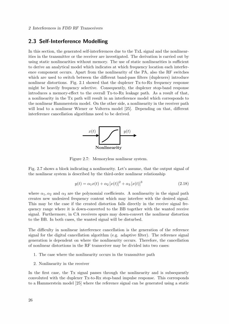
x(t) y(t)
Nonlinearity
Figure 2.7: Memoryless nonlinear system.
Fig. 2.7 shows a block indicating a nonlinearity. Let’s assume, that the output signal ofthe nonlinear system is described by the third-order nonlinear relationship
y(t) = α1x(t) + α2 [x(t)]2 + α3 [x(t)]3 (2.18)
where α1, α2 and α3 are the polynomial coefficients. A nonlinearity in the signal pathcreates new undesired frequency content which may interfere with the desired signal.This may be the case if the created distortion falls directly in the receive signal fre-quency range where it is down-converted to the BB together with the wanted receivesignal. Furthermore, in CA receivers spurs may down-convert the nonlinear distortionto the BB. In both cases, the wanted signal will be disturbed.
The difficulty in nonlinear interference cancellation is the generation of the referencesignal for the digital cancellation algorithm (e.g. adaptive filter). The reference signalgeneration is dependent on where the nonlinearity occurs. Therefore, the cancellationof nonlinear distortions in the RF transceiver may be divided into two cases:
1. The case where the nonlinearity occurs in the transmitter path
2. Nonlinearity in the receiver
In the first case, the Tx signal passes through the nonlinearity and is subsequentlyconvoluted with the duplexer Tx-to-Rx stop-band impulse response. This correspondsto a Hammerstein model [25] where the reference signal can be generated using a static
26
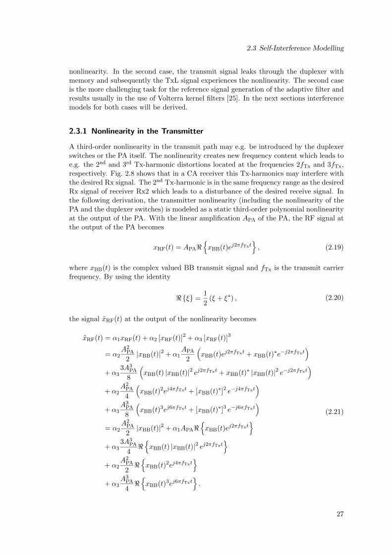
2.3 Self-Interference Modelling
nonlinearity. In the second case, the transmit signal leaks through the duplexer withmemory and subsequently the TxL signal experiences the nonlinearity. The second caseis the more challenging task for the reference signal generation of the adaptive filter andresults usually in the use of Volterra kernel filters [25]. In the next sections interferencemodels for both cases will be derived.
2.3.1 Nonlinearity in the Transmitter
A third-order nonlinearity in the transmit path may e.g. be introduced by the duplexerswitches or the PA itself. The nonlinearity creates new frequency content which leads toe.g. the 2nd and 3rd Tx-harmonic distortions located at the frequencies 2fTx and 3fTx,respectively. Fig. 2.8 shows that in a CA receiver this Tx-harmonics may interfere withthe desired Rx signal. The 2nd Tx-harmonic is in the same frequency range as the desiredRx signal of receiver Rx2 which leads to a disturbance of the desired receive signal. Inthe following derivation, the transmitter nonlinearity (including the nonlinearity of thePA and the duplexer switches) is modeled as a static third-order polynomial nonlinearityat the output of the PA. With the linear amplification APA of the PA, the RF signal atthe output of the PA becomes
xRF(t) = APA<xBB(t)ej2πfTxt
, (2.19)
where xBB(t) is the complex valued BB transmit signal and fTx is the transmit carrierfrequency. By using the identity
<ξ =1
2(ξ + ξ∗) , (2.20)
the signal xRF(t) at the output of the nonlinearity becomes
xRF(t) = α1xRF(t) + α2 [xRF(t)]2 + α3 [xRF(t)]3
= α2A2
PA
2|xBB(t)|2 + α1
APA
2
(xBB(t)ej2πfTxt + xBB(t)∗e−j2πfTxt
)
+ α33A3
PA
8
(xBB(t) |xBB(t)|2 ej2πfTxt + xBB(t)∗ |xBB(t)|2 e−j2πfTxt
)
+ α2A2
PA
4
(xBB(t)2ej4πfTxt + [xBB(t)∗]2 e−j4πfTxt
)
+ α3A3
PA
8
(xBB(t)3ej6πfTxt + [xBB(t)∗]3 e−j6πfTxt
)
= α2A2
PA
2|xBB(t)|2 + α1APA<
xBB(t)ej2πfTxt
+ α33A3
PA
4<xBB(t) |xBB(t)|2 ej2πfTxt
+ α2A2
PA
2<xBB(t)2ej4πfTxt
+ α3A3
PA
4<xBB(t)3ej6πfTxt
.
(2.21)
27
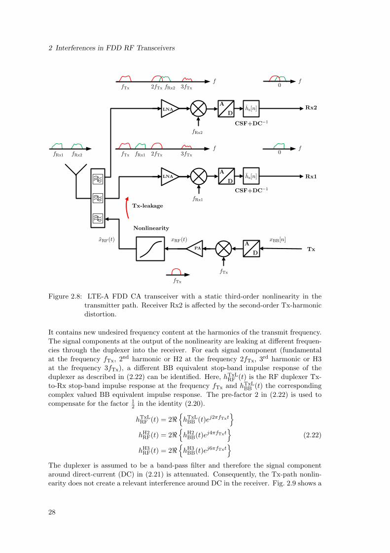
2 Interferences in FDD RF Transceivers
xBB[n]xRF(t)xRF(t)
Rx2
Rx1
Tx
Tx-leakage
Nonlinearity
A
D
A
D
A
D
fRx2
fRx1
fTx
fTx 2fTx fRx2 3fTx0
f f
fTx fRx1 2fTx 3fTx0
f ffRx1 fRx2
fTx
hs[n]
hs[n]
CSF+DC−1
CSF+DC−1
LNA
LNA
PA
Figure 2.8: LTE-A FDD CA transceiver with a static third-order nonlinearity in thetransmitter path. Receiver Rx2 is affected by the second-order Tx-harmonicdistortion.
It contains new undesired frequency content at the harmonics of the transmit frequency.The signal components at the output of the nonlinearity are leaking at different frequen-cies through the duplexer into the receiver. For each signal component (fundamentalat the frequency fTx, 2nd harmonic or H2 at the frequency 2fTx, 3rd harmonic or H3at the frequency 3fTx), a different BB equivalent stop-band impulse response of theduplexer as described in (2.22) can be identified. Here, hTxL
RF (t) is the RF duplexer Tx-to-Rx stop-band impulse response at the frequency fTx and hTxL
BB (t) the correspondingcomplex valued BB equivalent impulse response. The pre-factor 2 in (2.22) is used tocompensate for the factor 1
2 in the identity (2.20).
hTxLRF (t) = 2<
hTxL
BB (t)ej2πfTxt
hH2RF(t) = 2<
hH2
BB(t)ej4πfTxt
hH3RF(t) = 2<
hH3
BB(t)ej6πfTxt
(2.22)
The duplexer is assumed to be a band-pass filter and therefore the signal componentaround direct-current (DC) in (2.21) is attenuated. Consequently, the Tx-path nonlin-earity does not create a relevant interference around DC in the receiver. Fig. 2.9 shows a
28
2.3 Self-Interference Modelling
xRF(t) xRF(t) yRF(t)hRF(t)
Nonlinearity Duplexer
Figure 2.9: Nonlinear system and duplexer.
simplified block diagram of the signals and the duplexer impulse response. The receivedinterference signal after the duplexer is
yRF(t) = xRF(t) ∗ hRF(t)
= α1APA<[xBB(t) ∗ hTxL
BB (t)]ej2πfTxt
+ α33A3
PA
4<[xBB(t) |xBB(t)|2 ∗ hTxL
BB (t)]ej2πfTxt
+ α2A2
PA
2<[xBB(t)2 ∗ hH2
BB(t)]ej4πfTxt
+ α3A3
PA
4<[xBB(t)3 ∗ hH3
BB(t)]ej6πfTxt
,
(2.23)
which is amplified by the LNA with gain ALNA. The resulting LNA output signalbecomes
yRF,LNA(t) = ALNAyRF(t). (2.24)
For modeling purposes it is assuming that each interference component at frequencyψ · fTx for ψ = 1,2,3 is down-converted with an appropriate spur with amplitude Asp,ψ
and frequency fsp,ψ to the receiver BB2. The down-converted interference signals appearin the BB with the frequency shifts
f∆ψ= ψ · fTx − fsp,ψ. (2.25)
Consequently, each signal component is amplified with the combined LNA and spur gainGψ = ALNAAsp,ψ. The received signal after the down-conversion of each interference
2In practice, usually not for all interference components a corresponding spur occurs at the same time.
29
2 Interferences in FDD RF Transceivers
component yRF,LNA,ψ(t) with a corresponding spur becomes
yRF(t) =3∑
ψ=1
yRF,LNA,ψ(t) ·Asp,ψe−j2πfsp,ψ
= α1APAG1
2
[xBB(t) ∗ hTxL
BB (t)]ej2π(fTx−fsp,1)t
+[xBB(t) ∗ hTxL
BB (t)]∗e−j2π(fTx+fsp,1)t
+ α33A3
PAG1
8
[xBB(t) |xBB(t)|2 ∗ hTxL
BB (t)]ej2π(fTx−fsp,1)t
+[xBB(t) |xBB(t)|2 ∗ hTxL
BB (t)]∗e−j2π(fTx+fsp,1)t
+ α2A2
PAG2
4
[xBB(t)2 ∗ hH2
BB(t)]ej2π(2fTx−fsp,2)t
+[xBB(t)2 ∗ hH2
BB(t)]∗e−j2π(2fTx+fsp,2)t
+ α3A3
PAG3
8
[xBB(t)3 ∗ hH3
BB(t)]ej2π(3fTx−fsp,3)t
+[xBB(t)3 ∗ hH3
BB(t)]∗e−j2π(3fTx+fsp,3)t
,
(2.26)
where the ideally assumed anti-aliasing filter in front of the ADC attenuates the signalcomponents which are far away from the BB. The resulting received interference signalin discrete time at the output of the ADC is approximated by
yBB,ADC[n] = α1APAG1
2
[xBB[n] ∗ hTxL
BB [n]]ej2π
f∆1fs
n
+ α33A3
PAG1
8
[xBB[n] |xBB[n]|2 ∗ hTxL
BB [n]]ej2π
f∆1fs
n
+ α2A2
PAG2
4
[xBB[n]2 ∗ hH2
BB[n]]ej2π
f∆2fs
n
+ α3A3
PAG3
8
[xBB[n]3 ∗ hH3
BB[n]]ej2π
f∆3fs
n.
(2.27)
Here, fs is the sampling frequency and the baseband equivalent discrete-time duplexerimpulse response
hTxLBB [n] = Tsh
TxLBB (t)
∣∣t=nTs
(2.28)
is a scaled and sampled (impulse invariant) version of the continuous-time BB impulseresponse hTxL
BB (t) [34, 35]. The DC in the received signal is time-variant and has manysources like e.g. LO-LO self mixing [8]. Therefore, to prevent the ADC from saturation,the receiver contains a mixed-signal DC cancellation. This DC cancellation in combi-nation with the channel-select filtering is modeled by the combined impulse response
30
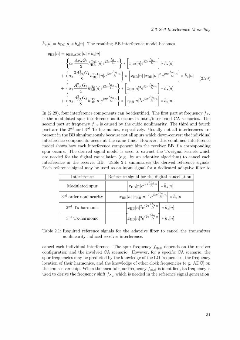
2.3 Self-Interference Modelling
hs[n] = hDC[n] ∗ hs[n]. The resulting BB interference model becomes
yBB[n] = yBB,ADC[n] ∗ hs[n]
=
α1APAG1
2hTxL
BB [n]ej2π
f∆1fs
n∗[xBB[n]e
j2πf∆1fs
n]∗ hs[n]
+
α3
3A3PAG1
8hTxL
BB [n]ej2π
f∆1fs
n∗[xBB[n] |xBB[n]|2 ej2π
f∆1fs
n]∗ hs[n]
+
α2A2
PAG2
4hH2
BB[n]ej2π
f∆2fs
n∗[xBB[n]2e
j2πf∆2fs
n]∗ hs[n]
+
α3A3
PAG3
8hH3
BB[n]ej2π
f∆3fs
n∗[xBB[n]3e
j2πf∆3fs
n]∗ hs[n].
(2.29)
In (2.29), four interference components can be identified. The first part at frequency fTx
is the modulated spur interference as it occurs in intra/inter-band CA scenarios. Thesecond part at frequency fTx is caused by the cubic nonlinearity. The third and fourthpart are the 2nd and 3rd Tx-harmonics, respectively. Usually not all interferences arepresent in the BB simultaneously because not all spurs which down-convert the individualinterference components occur at the same time. However, this combined interferencemodel shows how each interference component hits the receiver BB if a correspondingspur occurs. The derived signal model is used to extract the Tx-signal kernels whichare needed for the digital cancellation (e.g. by an adaptive algorithm) to cancel eachinterference in the receiver BB. Table 2.1 summarizes the derived reference signals.Each reference signal may be used as an input signal for a dedicated adaptive filter to
Interference Reference signal for the digital cancellation
Modulated spur
[xBB[n]e
j2πf∆1fs
n]∗ hs[n]
3rd order nonlinearity
[xBB[n] |xBB[n]|2 ej2π
f∆1fs
n]∗ hs[n]
2nd Tx-harmonic
[xBB[n]2e
j2πf∆2fs
n]∗ hs[n]
3rd Tx-harmonic
[xBB[n]3e
j2πf∆3fs
n]∗ hs[n]
Table 2.1: Required reference signals for the adaptive filter to cancel the transmitternonlinearity induced receiver interference.
cancel each individual interference. The spur frequency fsp,ψ depends on the receiverconfiguration and the involved CA scenario. However, for a specific CA scenario, thespur frequencies may be predicted by the knowledge of the LO frequencies, the frequencylocation of their harmonics, and the knowledge of other clock frequencies (e.g. ADC) onthe transceiver chip. When the harmful spur frequency fsp,ψ is identified, its frequency isused to derive the frequency shift f∆ψ
which is needed in the reference signal generation.
31
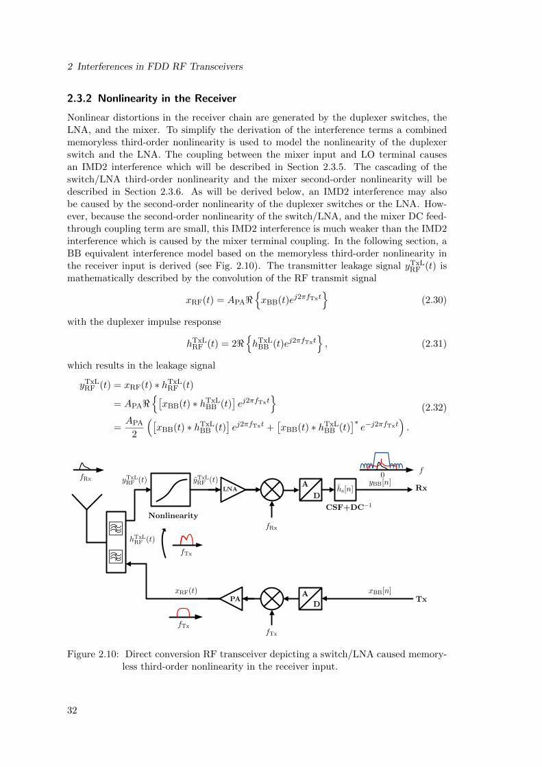
2 Interferences in FDD RF Transceivers
2.3.2 Nonlinearity in the Receiver
Nonlinear distortions in the receiver chain are generated by the duplexer switches, theLNA, and the mixer. To simplify the derivation of the interference terms a combinedmemoryless third-order nonlinearity is used to model the nonlinearity of the duplexerswitch and the LNA. The coupling between the mixer input and LO terminal causesan IMD2 interference which will be described in Section 2.3.5. The cascading of theswitch/LNA third-order nonlinearity and the mixer second-order nonlinearity will bedescribed in Section 2.3.6. As will be derived below, an IMD2 interference may alsobe caused by the second-order nonlinearity of the duplexer switches or the LNA. How-ever, because the second-order nonlinearity of the switch/LNA, and the mixer DC feed-through coupling term are small, this IMD2 interference is much weaker than the IMD2interference which is caused by the mixer terminal coupling. In the following section, aBB equivalent interference model based on the memoryless third-order nonlinearity inthe receiver input is derived (see Fig. 2.10). The transmitter leakage signal yTxL
RF (t) ismathematically described by the convolution of the RF transmit signal
xRF(t) = APA<xBB(t)ej2πfTxt
(2.30)
with the duplexer impulse response
hTxLRF (t) = 2<
hTxL
BB (t)ej2πfTxt, (2.31)
which results in the leakage signal
yTxLRF (t) = xRF(t) ∗ hTxL
RF (t)
= APA<[xBB(t) ∗ hTxL
BB (t)]ej2πfTxt
=APA
2
([xBB(t) ∗ hTxL
BB (t)]ej2πfTxt +
[xBB(t) ∗ hTxL
BB (t)]∗e−j2πfTxt
).
(2.32)
xBB[n]
yBB[n]0
LNA
PAxRF(t)
hTxLRF (t)
yTxLRF (t) yTxL
RF (t)A
D
A
D
fTx
fTx
fTx
fRx
fRx
Rx
f0
Tx
NonlinearityCSF+DC−1
hs[n]
Figure 2.10: Direct conversion RF transceiver depicting a switch/LNA caused memory-less third-order nonlinearity in the receiver input.
32
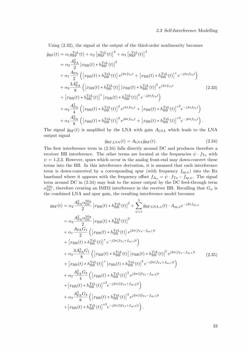
2.3 Self-Interference Modelling
Using (2.32), the signal at the output of the third-order nonlinearity becomes
yRF(t) = α1yTxLRF (t) + α2
[yTxL
RF (t)]2
+ α3
[yTxL
RF (t)]3
= α2A2
PA
2
∣∣xBB(t) ∗ hTxLBB (t)
∣∣2
+ α1APA
2
([xBB(t) ∗ hTxL
BB (t)]ej2πfTxt +
[xBB(t) ∗ hTxL
BB (t)]∗e−j2πfTxt
)
+ α33A3
PA
8
([xBB(t) ∗ hTxL
BB (t)] ∣∣xBB(t) ∗ hTxL
BB (t)∣∣2 ej2πfTxt
+[xBB(t) ∗ hTxL
BB (t)]∗ ∣∣xBB(t) ∗ hTxL
BB (t)∣∣2 e−j2πfTxt
)
+ α2A2
PA
4
([xBB(t) ∗ hTxL
BB (t)]2ej4πfTxt +
[xBB(t) ∗ hTxL
BB (t)]∗2e−j4πfTxt
)
+ α3A3
PA
8
([xBB(t) ∗ hTxL
BB (t)]3ej6πfTxt +
[xBB(t) ∗ hTxL
BB (t)]∗3e−j6πfTxt
).
(2.33)
The signal yRF(t) is amplified by the LNA with gain ALNA which leads to the LNAoutput signal
yRF,LNA(t) = ALNAyRF(t). (2.34)
The first interference term in (2.34) falls directly around DC and produces therefore areceiver BB interference. The other terms are located at the frequencies ψ · fTx withψ = 1,2,3. However, spurs which occur in the analog front-end may down-convert theseterms into the BB. In this interference derivation, it is assumed that each interferenceterm is down-converted by a corresponding spur (with frequency fsp,ψ) into the Rxbaseband where it appears with the frequency offset f∆ψ
= ψ · fTx − fsp,ψ. The signalterm around DC in (2.34) may leak to the mixer output by the DC feed-through termαMix
DC , therefore creating an IMD2 interference in the receiver BB. Recalling that Gψ isthe combined LNA and spur gain, the resulting interference model becomes
yRF(t) = α2A2
PAαMixDC
2
∣∣xBB(t) ∗ hTxLBB (t)
∣∣2 +3∑
ψ=1
yRF,LNA,ψ(t) ·Asp,ψe−j2πfsp,ψ
= α2A2
PAαMixDC
2
∣∣xBB(t) ∗ hTxLBB (t)
∣∣2
+ α1APAG1
2
([xBB(t) ∗ hTxL
BB (t)]ej2π(fTx−fsp,1)t
+[xBB(t) ∗ hTxL
BB (t)]∗e−j2π(fTx+fsp,1)t
)
+ α33A3
PAG1
8
([xBB(t) ∗ hTxL
BB (t)] ∣∣xBB(t) ∗ hTxL
BB (t)∣∣2 ej2π(fTx−fsp,1)t
+[xBB(t) ∗ hTxL
BB (t)]∗ ∣∣xBB(t) ∗ hTxL
BB (t)∣∣2 e−j2π(fTx+fsp,1)t
)
+ α2A2
PAG2
4
([xBB(t) ∗ hTxL
BB (t)]2ej2π(2fTx−fsp,2)t
+[xBB(t) ∗ hTxL
BB (t)]∗2e−j2π(2fTx+fsp,2)t
)
+ α3A3
PAG3
8
([xBB(t) ∗ hTxL
BB (t)]3ej2π(3fTx−fsp,3)t
+[xBB(t) ∗ hTxL
BB (t)]∗3e−j2π(3fTx+fsp,3)t
).
(2.35)
33
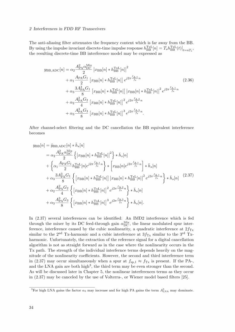
2 Interferences in FDD RF Transceivers
The anti-aliasing filter attenuates the frequency content which is far away from the BB.By using the impulse invariant discrete-time impulse response hTxL
BB [n] = TshTxLBB (t)
∣∣t=nTs
,the resulting discrete-time BB interference model may be expressed as
yBB,ADC[n] = α2A2
PAαMixDC
2
∣∣xBB[n] ∗ hTxLBB [n]
∣∣2
+ α1APAG1
2
[xBB[n] ∗ hTxL
BB [n]]ej2π
f∆,1fs
n(2.36)
+ α33A3
PAG1
8
[xBB[n] ∗ hTxL
BB [n]] ∣∣xBB[n] ∗ hTxL
BB [n]∣∣2 ej2π
f∆,1fs
n
+ α2A2
PAG2
4
[xBB[n] ∗ hTxL
BB [n]]2ej2π
f∆,2fs
n
+ α3A3
PAG3
8
[xBB[n] ∗ hTxL
BB [n]]3ej2π
f∆,3fs
n.
After channel-select filtering and the DC cancellation the BB equivalent interferencebecomes
yBB[n] = yBB,ADC[n] ∗ hs[n]
= α2A2
PAαMixDC
2
∣∣xBB[n] ∗ hTxLBB [n]
∣∣2∗ hs[n]
+
α1APAG1
2hTxL
BB [n]ej2π
f∆,1fs
n∗[xBB[n]e
j2πf∆,1fs
n]∗ hs[n]
+ α33A3
PAG1
8
[xBB[n] ∗ hTxL
BB [n]] ∣∣xBB[n] ∗ hTxL
BB [n]∣∣2 ej2π
f∆,1fs
n∗ hs[n]
+ α2A2
PAG2
4
[xBB[n] ∗ hTxL
BB [n]]2ej2π
f∆,2fs
n∗ hs[n]
+ α3A3
PAG3
8
[xBB[n] ∗ hTxL
BB [n]]3ej2π
f∆,3fs
n∗ hs[n].
(2.37)
In (2.37) several interferences can be identified: An IMD2 interference which is fedthrough the mixer by its DC feed-through gain αMix
DC , the linear modulated spur inter-ference, interference caused by the cubic nonlinearity, a quadratic interference at 2fTx
similar to the 2nd Tx-harmonic and a cubic interference at 3fTx similar to the 3rd Tx-harmonic. Unfortunately, the extraction of the reference signal for a digital cancellationalgorithm is not as straight forward as in the case where the nonlinearity occurs in theTx path. The strength of the individual interfernce terms depends heavily on the mag-nitude of the nonlinearity coefficients. However, the second and third interference termin (2.37) may occur simultaneously when a spur at fsp,1 ≈ fTx is present. If the PA-,and the LNA gain are both high3, the third term may be even stronger than the second.As will be discussed later in Chapter 5, the nonlinear interferences terms as they occurin (2.37) may be canceled by the use of Volterra-, or Wiener model based filters [25].
3For high LNA gains the factor α3 may increase and for high PA gains the term A3LNA may dominate.
34
2.3 Self-Interference Modelling
2.3.3 Spur IQ-Imbalance
Till now it was assumed that the spur which is down-converting the RF interference tothe BB may be modeled as an equivalent complex valued spur of the form
psp(t) = Aspe−j2πfspt
= Asp (cos (2πfspt)− jsin(2πfspt))(2.38)
with amplitude Asp and frequency fsp. However, measurements at the real transceiverchip showed that the observed BB interference not only contains the down-convertedRF interference but also its spectral image. This means that the spur model needs tobe extended to be able to describe the true BB interference. This may be done byincorporating the IQ-imbalance model [36, 37]. By including a gain imbalance g, andphase imbalance φ, the spur model becomes
psp(t) = Asp (cos (2πfspt)− j g sin (2πfspt+ φ)) . (2.39)
By using the identities cos (ψ) = 12
(ejψ + e−jψ
)and sin (ψ) = 1
2j
(ejψ − e−jψ
)the spur
may be expressed as
psp(t) = Asp
[1
2
(ej2πfspt + e−j2πfspt
)− g
2
(ej(2πfspt+φ) − e−j(2πfspt+φ)
)]
= Asp
[K1e
−j2πfspt +K2ej2πfspt
] (2.40)
where
K1 =1 + g e−jφ
2, and K2 =
1− g ejφ2
. (2.41)
When (2.40) is used to replace the spur terms in (2.26) or (2.35), the resulting main andimage interference component appear in the BB. In Section 2.3.4, the modulated spurinterference including an IQ-imbalance in the spur will be derived in detail.
2.3.4 Modulated Spur Interference with Spur IQ-Imbalance
In this section, the modulated spur interference which was derived in Section 2.3.1 isextended by a spur IQ-imbalance. In the introduction of this thesis it was alreadymentioned that the modulated spur interference may be generated by LO-LO cross-talkspurs, or by the use of a split-LNA. In the following derivation it is assumed that themodulated spur interference is generated by an LO-LO cross-talk spur. Also the wantedRx signal and the noise are added in the interference model. Using the same modeling asintroduced in Section 2.3.1, the RF transmitter leakage signal into the receiver becomes
yTxLRF (t) = APA<
[xBB(t) ∗ hTxL
BB (t)]ej2πfTxt
. (2.42)
The LNA output signal
yTotRF,LNA(t) = ALNA
[yTxL
RF (t) + yRxRF(t) + vRF(t)
](2.43)
contains the amplified TxL signal yTxLRF (t), the wanted Rx signal yRx
RF(t) and the noisevRF(t). In the next step, the signal after the down-conversion mixer (2.44) is derived.
35
2 Interferences in FDD RF Transceivers
The wanted Rx and the noise signal are down-converted by the Rx mixer local oscillator,whereas the TxL signal is down-converted by the spur with IQ-imbalance (2.40) whichappears at the Rx mixer4. The TxL signal is amplified by Gsp = ALNAAsp, where Asp
is the spur gain. By neglecting the mixing products of the Rx and noise signal with thespur, the total received signal at the output of the mixer becomes
yTotRF,mixer(t) = yTxL
RF (t)Gsp
[K1e
−j2πfspt +K2e+j2πfspt
]
+ALNA
[yRx
RF(t) + vRF(t)]e−j2πfRxt.
(2.44)
Using the identity <ξ = 12 (ξ + ξ∗), (2.44) results in
yTotRF,mixer(t) =
APAGsp
2
K1
[xBB(t) ∗ hTxL
BB (t)]ej2π(fTx−fsp)t
+K2
[xBB(t) ∗ hTxL
BB (t)]ej2π(fTx+fsp)t
+K1
[xBB(t) ∗ hTxL
BB (t)]∗e−j2π(fTx+fsp)t
+K2
[xBB(t) ∗ hTxL
BB (t)]∗e−j2π(fTx−fsp)t
(2.45)
+ALNA
[1
2yRx
BB(t) +1
2yRx
BB(t)∗e−j4πfRxt
]
+ALNA
[1
2vBB(t) +
1
2vBB(t)∗e−j4πfRxt
].
The ideally assumed anti-aliasing filter in front of the ADC attenuates the mixing prod-ucts in yTot
RF,mixer(t) which are far away from the BB. The resulting received discrete-timesignal using (2.22) and (2.28) is approximated by
yTotBB,ADC[n] =
APAGsp
2
K1
[xBB[n] ∗ hTxL
BB [n]]ej2π
f∆fsn
+ K2
[xBB[n] ∗ hTxL
BB [n]]∗e−j2π f∆
fsn
+ALNA
2yRx
BB[n] +ALNA
2vBB[n],
(2.46)
where f∆ = fTx − fsp. Thus, the main modulated spur interference component appearsin the receiver BB with the frequency offset f∆, and the image with the offset −f∆.Considering the combined channel-select filtering and DC-cancellation with the impulseresponse hs[n], (2.46) leads to the BB equivalent received signal
yTotBB [n] = yTot
BB,ADC[n] ∗ hs[n]
= xsBB[n] ∗ hTot
BB,1[n] + xs*BB[n] ∗ hTot
BB,2[n]︸ ︷︷ ︸
yMSBB
+ALNA
2yRx
BB[n] ∗ hs[n] +ALNA
2vBB[n] ∗ hs[n].
(2.47)
4In the real mixing process the overall signal which appears at the mixer input (including the Rx, thenoise and the TxL signal) is mixed with the LO frequency and the spur. However, some of the mixingproducts fall outside the relevant frequency range and may be neglected.
36
2.3 Self-Interference Modelling
In this final result yMSBB is the BB equivalent modulated spur interference which contains
a main and an image interference component. In
xsBB[n] =
[xBB[n]e
j2πf∆fsn]∗ hs[n], (2.48)
the Tx signal is shifted by f∆ and subsequently filtered by the CSF and
hTotBB,1[n] =
APAGspK1
2hTxL
BB [n]ej2π
f∆fsn, (2.49)
hTotBB,2[n] =
APAGspK2
2hTxL
BB [n]e−j2π f∆
fsn
(2.50)
are the main and image impulse responses of the Tx-to-Rx leakage channel. The digitalcancellation of this modulated spur interference by adaptive filtering is presented inSection 4.6.
2.3.5 Mixer Terminal Coupling Induced IMD2
The second-order nonlinearity of the switch/LNA creates an IMD2 interference whichmay leak through the mixer DC feed-through to the BB. However, the larger contri-bution of IMD2 interference is created by a coupling between the RF and LO port ofthe IQ-mixer [8]. Based on the block diagram in Fig. 2.11 depicting an RF transceiveroperating in FDD mode, a detailed IMD2 interference model is derived. The transmittedcomplex valued BB signal xBB(t) = xI(t) + jxQ(t) is up-converted to the passband andamplified by the PA gain APA which is for simplicity assumed to be linear (neglectingthe transmitter nonlinearity). The resulting RF transmit signal
xRF(t) = APA<xBB(t)ej2πfTxt
(2.51)
is radiated by the antenna, but a small portion of the signal is leaking through theduplexer stop-band which is modeled by the RF impulse response
hTxLRF (t) = 2<
hTxL
BB (t)ej2πfTxt, (2.52)
where hTxLBB (t) is the BB equivalent duplexer impulse response. The resulting transmitter
leakage signal in the receiver can be expressed as
yTxLRF (t) = xRF(t) ∗ hTxL
RF (t)
= APA<[xBB(t) ∗ hTxL
BB (t)]ej2πfTxt
.
(2.53)
The total received signal at the output of the LNA
yTotRF,LNA(t) = ALNA
[yTxL
RF (t) + yRxRF(t) + vRF(t)
], (2.54)
with the gain ALNA contains the amplified Tx leakage signal, the wanted Rx signalyRx
RF(t) and the noise vRF(t). The output signal of the I-, and Q-path mixer is combinedinto the complex valued signal yTot
RF,mixer(t) (2.55). It contains the wanted signal which
is down-converted with the linear gain α1 = αI1 = αQ
1 , and the second order interference
37
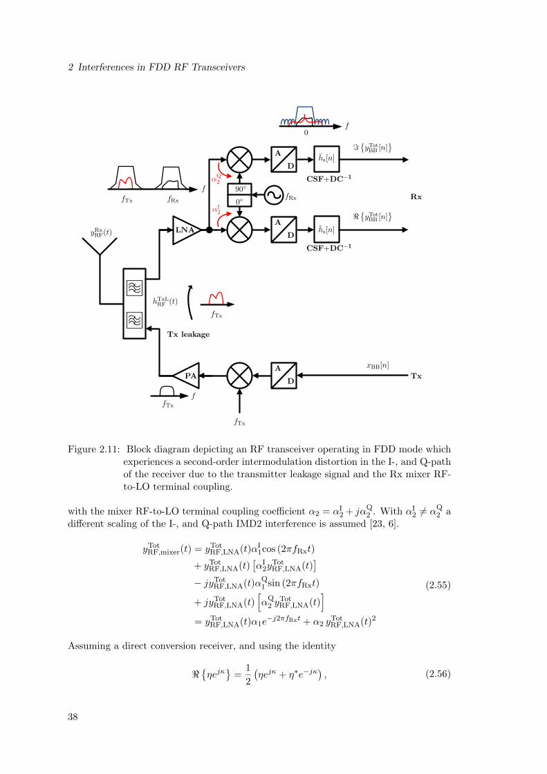
2 Interferences in FDD RF Transceivers
xBB[n]
yRxRF(t)
<yTot
BB [n]
=yTot
BB [n]
LNA
PA
hs[n]
hs[n]
CSF+DC−1
CSF+DC−1
hTxLRF (t)
A
D
A
D
A
D
Tx leakage
fTx
fTx
fTx
fTx
fRxfRx
90
0
αI2
αQ2
f
f
0f
Rx
Tx
Figure 2.11: Block diagram depicting an RF transceiver operating in FDD mode whichexperiences a second-order intermodulation distortion in the I-, and Q-pathof the receiver due to the transmitter leakage signal and the Rx mixer RF-to-LO terminal coupling.
with the mixer RF-to-LO terminal coupling coefficient α2 = αI2 + jαQ
2 . With αI2 6= αQ
2 adifferent scaling of the I-, and Q-path IMD2 interference is assumed [23, 6].
yTotRF,mixer(t) = yTot
RF,LNA(t)αI1cos (2πfRxt)
+ yTotRF,LNA(t)
[αI
2yTotRF,LNA(t)
]
− jyTotRF,LNA(t)αQ
1 sin (2πfRxt)
+ jyTotRF,LNA(t)
[αQ
2 yTotRF,LNA(t)
]
= yTotRF,LNA(t)α1e
−j2πfRxt + α2 yTotRF,LNA(t)2
(2.55)
Assuming a direct conversion receiver, and using the identity
<ηejκ
=
1
2
(ηejκ + η∗e−jκ
), (2.56)
38
2.3 Self-Interference Modelling
the total mixer output signal by neglecting the signal content which falls outside the BBbandwidth becomes
yTotRF,mixer(t) = α1
ALNA
2yRx
BB(t) + α1ALNA
2vBB(t)
+α2A
2LNA
2
[∣∣APA
(xBB(t) ∗ hTxL
BB (t))∣∣2 +
∣∣yRxBB(t)
∣∣2
+ |vBB(t)|2 + 2<yRx
BB(t)v∗BB(t)].
(2.57)
The third term in (2.57) contains the squared envelope of the TxL signal denoted as theIMD2 interference. As in critical, e.g., cell edge scenarios the Rx and noise signal aremuch weaker than the TxL signal, the last three terms in (2.57) may be neglected [6, 7].The resulting total received discrete time BB signal
yTotBB [n] = α1
ALNA
2yRx
BB[n] ∗ hs[n] + α1ALNA
2vBB[n] ∗ hs[n]
+α2
2
∣∣ALNAAPA
(xBB[n] ∗ hTxL
BB [n])∣∣2 ∗ hs[n]
︸ ︷︷ ︸yIMD2BB [n]
, (2.58)
contains the BB IMD2 interference yIMD2BB [n] and includes the DC cancellation and
channel-select filtering using the combined impulse response hs[n]. In (2.58) it canbe observed, that the IMD2 interference is generated by the squared envelope of theBB equivalent TxL signal. This squared envelope contains a DC and has twice the Txsignal bandwidth (BW). The DC is eliminated in the receiver by its mixed-signal DCcancellation and the BW is reduced to the LTE signal BW by the CSF.
39
2 Interferences in FDD RF Transceivers
2.3.6 Higher Even-Order Intermodulation Interferences
Cascading the third-order nonlinearity of the switch/LNA (Section 2.3.2), with thesecond-order nonlinearity of the mixer (Section 2.3.5), additional nonlinear interfer-ence terms occur. The output signal of the LNA including a third-order polynomialnonlinearity and by neglecting the intermodulation products of the Rx and noise signalbecomes
yTotRF,LNA(t) = ALNAy
TxLRF (t) + αLNA
2
[yTxL
RF (t)]2
+ αLNA3
[yTxL
RF (t)]3
+ALNA
[yRx
RF(t) + vRF(t)]
= αLNA2
A2PA
2
∣∣xBB(t) ∗ hTxLBB (t)
∣∣2
+ALNAAPA
2
([xBB(t) ∗ hTxL
BB (t)]ej2πfTxt +
[xBB(t) ∗ hTxL
BB (t)]∗e−j2πfTxt
)
+ αLNA3
3A3PA
8
([xBB(t) ∗ hTxL
BB (t)] ∣∣xBB(t) ∗ hTxL
BB (t)∣∣2 ej2πfTxt
+[xBB(t) ∗ hTxL
BB (t)]∗ ∣∣xBB(t) ∗ hTxL
BB (t)∣∣2 e−j2πfTxt
)
+ αLNA2
A2PA
4
([xBB(t) ∗ hTxL
BB (t)]2ej4πfTxt +
[xBB(t) ∗ hTxL
BB (t)]∗2e−j4πfTxt
)
+ αLNA3
A3PA
8
([xBB(t) ∗ hTxL
BB (t)]3ej6πfTxt +
[xBB(t) ∗ hTxL
BB (t)]∗3e−j6πfTxt
)
+ALNA
[yRx
RF(t) + vRF(t)].
(2.59)With the mixer RF-to-LO terminal coupling coefficient αMix
2 = αI2 + jαQ2 for the I- andQ-branch of the IQ mixer, the down-conversion gain αMix
15, and the DC feed-through
gain αMixDC = αIDC + jαQDC, the output signal of the mixer becomes
yTotRF,mixer(t) = αMix
DC yTotRF,LNA(t) + yTot
RF,LNA(t)αMix1 e−j2πfRxt + αMix
2 yTotRF,LNA(t)2. (2.60)
Neglecting the signal components which are outside the CSF bandwidth, the total re-ceived BB signal may be described by
yTotRF,mixer(t) =
A2PA
2
(αMix
2 A2LNA + αLNA
2 αMixDC
) ∣∣xBB(t) ∗ hTxLBB (t)
∣∣2
+ αMix2
A4PA
8
[3(αLNA
2
)2+ 6αLNA
3 ALNA
] ∣∣xBB(t) ∗ hTxLBB (t)
∣∣4
+ αMix2
(αLNA
3
)2 10A6PA
32
∣∣xBB(t) ∗ hTxLBB (t)
∣∣6
+ αMix1
ALNA
2yRx
BB(t) + αMix1
ALNA
2vBB(t).
(2.61)
5An identical down-conversion gain for the I-, and Q-branch is assumed.
40
2.4 Quantification of the IMD2 Interference
The resulting total received discrete time BB signal after the combined channel-select-,and DC-filtering using hs[n] = hs[n] ∗ hDC[n] is approximated by
yTotBB [n] =
[A2
PA
2
(αMix
2 A2LNA + αLNA
2 αMixDC
) ∣∣xBB[n] ∗ hTxLBB [n]
∣∣2]∗ hs[n]
+
[αMix
2
A4PA
8
[3(αLNA
2
)2+ 6αLNA
3 ALNA
] ∣∣xBB[n] ∗ hTxLBB [n]
∣∣4]∗ hs[n]
+
[αMix
2
(αLNA
3
)2 10A6PA
32
∣∣xBB[n] ∗ hTxLBB [n]
∣∣6]∗ hs[n]
+
[αMix
1
ALNA
2yRx
BB[n] + αMix1
ALNA
2vBB[n]
]∗ hs[n].
(2.62)
The first term in (2.62) corresponds to the IMD2 interference. It is generated by thesecond-order nonlinearity of the mixer and the combination of the second-order non-linearity of the LNA and the DC feed-through of the mixer. The second term is thefourth-order intermodulation distortion (IMD4) interference which is a combination ofthe second-order-, and third-order nonlinearity of the LNA and the second-order nonlin-earity of the mixer. The third term is the sixth-order intermodulation distortion (IMD6)interference which is generated by the third-order nonlinearity of the LNA in combina-tion with the second-order nonlinearity of the mixer.
2.4 Quantification of the IMD2 Interference
2.4.1 Two-Tone IIP2 Derivation
The second-order intermodulation product (IM2) is created by the quadratic nonlinearityof the mixer [38]. At the output of the mixer, undesired frequency content is generatedbut only the signal part which falls into the BB interferes with the desired Rx signal.The second-order receiver nonlinearity is typically specified by the two-tone second-orderinput intercept point (IIP2) value [39]. This value determines at which input power levelthe total input power Pin = A2/Z0 of the two-tone (2t) RF input signal
x(t) = Acos (2πf1t) +Acos (2πf2t) (2.63)
equals the total mixer input-referred6 IM2 power. It also allows the calculation of themixer input-referred two-tone IM2 signal power by the well known formula [39]
PTot,2tIM2,dBm = 2Pin,dBm − IIP2dBm (2.64)
6The IMD2 signal power which occurs at the output of the nonlinear mixer may be related to anequivalent power at the input of the mixer which (when amplified with the linear power gain α2
1
of the mixer) generates the same IMD2 output power. This so-called input-referred IMD2 power isobtained by dividing the mixer IMD2 output power PTot,2t,OR
IM2 by α21.
41
2 Interferences in FDD RF Transceivers
derived in the following. The mixer output signal
y(t) = x(t)α1e−j2πfRxt + α2x(t)2
= x(t)α1e−j2πfRxt︸ ︷︷ ︸
ylin(t)
+α2
2A2 cos (4πf1t) + cos (4πf2t)
︸ ︷︷ ︸2nd harmonics
+ α2A2 1 + cos (2π [f1 + f2] t) + cos (2π [f2 − f1] t)︸ ︷︷ ︸
yTot,2tIM2 (t)
(2.65)
consists of the linearly down-converted input signal ylin(t), the 2nd order harmonics, andthe two-tone IM2 signal. The resulting mixer output-referred (OR) IM2 signal powerbecomes
PTot,2t,ORIM2 =
EyTot,2t
IM2 (t)2
Z0=
2α22A
4
Z0. (2.66)
At the IIP2 input power it holds that the input power Pin equals the input-referred IM2power:
Pin!
=1
α21
PTot,2t,ORIM2 =
2α22A
4
α21Z0
(2.67)
Inserting the input signal amplitude A2IIP2 = Pin,IIP2Z0 and solving for α2 results in
α2 =
√α2
1
2Pin,IIP2 Z0=
√α2
1
2 IIP2W Z0= 0.0316
1
V, (2.68)
for a down-conversion gain of 0 dBm (α1 = 1), a typical mixer IIP2 of +40dBm [40, 6],and the network impedance Z0 = 50Ω. By rearranging (2.68), the corresponding IIP2in watts becomes
IIP2W =α2
1
2α22Z0
. (2.69)
The mixer input-referred total IM2 power may be expressed by the input power Pin andthe IIP2W value:
PTot,2tIM2 =
1
α21
PTot,2t,ORIM2 =
2α22A
4
α21Z0
=P 2
in
IIP2W(2.70)
Finally, (2.70) leads to the input-referred IM2 power in dBm
PTot,2tIM2,dBm = 2Pin,dBm − IIP2dBm. (2.71)
The derivation of α2 from a given two-tone IIP2 value is required for the simulations inChapter 5 where a BB equivalent IMD2 interference in the time domain is generated.
42
2.4 Quantification of the IMD2 Interference
2.4.2 Modulated IMD2 Distortion
In this section, the TxL signal induced IMD2 signal power is derived to be able tobring it in relation with the two-tone IM2 power PTot,2t
IM2 (2.71). As a first step weneed to understand the relationship between the RF TxL signal power PTxL
RF and thecorresponding BB equivalent TxL signal power PTxL
BB at the mixer input (LNA output).The RF TxL signal at the LNA output is
yTxLRF,LNA(t) =ALNAAPA<
[xBB(t) ∗ hTxL
BB (t)]ej2πfTxt
, (2.72)
which has the power
Pin = PTxLRF,LNA =
1
Z0EyTxL
RF,LNA(t)2
=1
Z0E
(ALNAAPA<
[xBB(t) ∗ hTxL
BB (t)]ej2πfTxt
)2
=1
2
1
Z0EALNAAPA
∣∣xBB(t) ∗ hTxLBB (t)
∣∣2
︸ ︷︷ ︸=PTxL
BB,LNA
.
(2.73)
It can be observed, that the RF TxL signal power is half of the corresponding complexvalued BB equivalent TxL signal power7. The total IMD2 interference signal at theoutput of the mixer according to (2.58) (with twice the Tx signal BW and including theDC) is
yIMD2BB (t) =
α2
2
∣∣ALNAAPA xBB(t) ∗ hTxLBB (t)
∣∣2 . (2.74)
The resulting mixer OR IMD2 interference power becomes
PTot,mod,ORIMD2 =
1
Z0E
(α2
2
∣∣ALNAAPA xBB(t) ∗ hTxLBB (t)
∣∣2)2
=1
Z0
α22
4E∣∣ALNAAPA xBB(t) ∗ hTxL
BB (t)∣∣4.
(2.75)
By using the identity
EX4
= 2EX22 (2.76)
which holds for a scalar complex valued and zero-mean Gaussian distributed randomvariable X [41, 42, 43], the OR IMD2 power becomes
PTot,mod,ORIMD2 =
1
Z0
α22
2E∣∣ALNAAPA xBB(t) ∗ hTxL
BB (t)∣∣22. (2.77)
7Assuming an RF TxL signal power of -7 dBm, the corresponding power of the complex BB equivalentTxL signal is -4 dBm.
43
2 Interferences in FDD RF Transceivers
At the input power Pin,IIP2 (2.73), which has the value of the IIP2W, the input powerequals the input-referred IMD2 interference power:
Pin,IIP2!
=1
α21
PTot,mod,ORIMD2
1
2
1
Z0EALNAAPA
∣∣xBB(t) ∗ hTxLBB (t)
∣∣2
=α2
2
2α21Z0
E∣∣ALNAAPA xBB(t) ∗ hTxL
BB (t)∣∣22
1
Z0=α2
2
α21
1
Z0E∣∣ALNAAPA xBB(t) ∗ hTxL
BB (t)∣∣2
︸ ︷︷ ︸=2Pin,IIP2=2 IIP2W
(2.78)Rearranging (2.78) leads to the IIP2 value
IIP2W =α2
1
2α22Z0
, (2.79)
which is exactly the same as in the two-tone signal case. The resulting mixer input-referred IMD2 interference power (with twice the Tx signal BW and including the DC)which is generated by the modulated RF TxL signal becomes
PTot,modIMD2,dBm = 2PTxL
RF,LNA − IIP2dBm. (2.80)
However, care has to be taken in simulations where the BB equivalent signals are usedinstead of the RF signals. It is quite common [44]8 to set the power of the BB equivalentTxL signals to the power of the RF TxL signal (not scaled to twice of the correspondingRF TxL signal power as stated in (2.73)). Then, the IMD2 signal power obtained in theBB equivalent simulation corresponds to
PTot,modIMD2,dBm = 2(PTxL
RF,LNA − 3 dB)− IIP2dBm
= 2PTxLRF,LNA − IIP2dBm − 6 dB.
(2.81)
Because the TxL signal is typically non-Gaussian distributed, the correction factor CFdist
is introduced which accounts for the violation of (2.76). The resulting IMD2 signal powerbecomes
PTot,modIMD2,dBm = 2PTxL
RF,LNA − IIP2dBm − 6 dB− CFdist. (2.82)
The reduction of the total IMD2 power in case of non-Gaussian distributed Tx signals(e.g. orthogonal frequency-division multiplexing (OFDM) or single-carrier frequency-division multiple access (SC-FDMA) modulated) is summarized in Table 2.2. AfterDC-, and channel-select filtering, the modulated IMD2 interference power is furtherreduced by 6 dB if the total IMD2 signal spectrum with twice the Tx BW is assumedflat and has half of the power at DC. If the spectrum is non-flat, which typically is thecase, the IMD2 power needs to be corrected by the factor CFflat which leads to the finalestimate
PTot,mod,CSFIMD2,dBm = 2PTxL
RF,LNA − IIP2dBm − 12 dB− CFdist − CFflat (2.83)
8In this publication, the Tx signal induced IMD2 signal power is compared between a two-tone-, anda modulated Tx signal. The modulated RF Tx signal power is set to half of the two-tone RF signalpower. This implies that the modulated complex BB equivalent Tx signal has the same power as thetwo-tone RF signal (see Fig. 2 in [44]).
44
2.4 Quantification of the IMD2 Interference
Table 2.2: Reduction of IMD2 power due to non-Gaussian distributed TxL signal: Fullallocated 10 MHz Tx signal
SC-FDMATx distribution Gaussian OFDM QPSK 16QAM 64QAM
CFdist (dB) 0 0 0.72 0.51 0.48
of the DC-, and channel-select filtered IMD2 interference power. In [39, 45], the equation
PTot,mod,CSFIMD2,dBm = 2PTxL
RF,LNA − IIP2dBm − CF, (2.84)
is used to estimate the DC-, and channel-select filtered IMD2 power, where the correctionfactor CF is obtained by simulations and verified by measurements, but not derived indetail as in (2.83). The estimated CF for W-CDMA Tx signals is 13.7 dB and 15.7 dBin [39] and [45], respectively. The authors in [44] derived the IIP2 requirements for4G handset receivers by using a combined correction factor of 11 dB and 13.7 dB for10 MHz SC-FDMA (LTE) and WCDMA modulated Tx signals, respectively. It has tobe mentioned, that in [44] the ideal Tx signals are used9 to obtain the correction factors.With (2.83) it is possible to estimate the IMD2 power and thereby the resulting Rxsignal-to-interference-plus-noise ratio (SINR)
SINRdB = 10 log10
(PRx
PTot,mod,CSFIMD2 + Pn
)
= PRx,dBm − 10 log10
(PTot,mod,CSF
IMD2 + Pn1mW
) (2.85)
when the Tx power increases. Assuming an Rx signal with -90 dBm with a signal-to-noise ratio (SNR) of 10 dB, an SC-FDMA LTE Tx signal with QPSK modulation(CFdist = 0.72 dBm), LNA gain of 20 dB, an average duplexer isolation of 50 dB, mixerIIP2 of +40 dBm and using CFflat = 0.67 dBm (duplexer dependent), the resulting RxSINR with increasing Tx power may be estimated as summarized in Table 2.3. Thecombined correction factor is obtained by CF = 12 dB + CFdist + CFflat = 13.4 dB.
Table 2.3: Drop of the Rx SINR due to the Tx induced IMD2 interference which isgenerated by a fully allocated 10 MHz LTE Tx signal
PTxBB (dBm) 0 6 12 18 23
PTot,mod,CSFIMD2 (dBm) -113.4 -101.4 -89.4 -77.4 -67.4
SINR (dB) 9.99 9.96 9.52 5.5 -2.84
9No frequency-selective duplexer Tx-to-Rx stop-band response is used to generate a TxL signal.
45
2 Interferences in FDD RF Transceivers
2.4.3 IIP2 Characterization
The receiver IIP2 is characterized by using two cosine signals at the input of the nonlinearmixer with the frequencies f1 and f2 of equal amplitude A and the combined power Pin,2t.The resulting total IMD2 power in dBm generated at DC, f1 + f2 and f2 − f1 at theoutput of the mixer can be calculated by PTot,2t
IM2 = 2Pin,2t − IIP2 [45]. Here, half ofthe total IMD2 power falls to DC, and one quarter each to f1 + f2 and f2 − f1. Tocharacterize the IIP2 in a zero-IF receiver, the frequencies f1 and f2 are chosen suchthat f2−f1 falls within the CSF bandwidth. Thereby the power P f2−f1
IM2 at the frequency
f2 − f1 is measured and the IIP2 is determined by IIP2 = 2Pin,2t − P f2−f1
IM2 − 6 dB.
2.4.4 Severity of the IMD2 Interference
For modulated TxL signals, the BB IMD2 signal power is modulation dependent andfurther reduced by the DC cancellation and channel-select filtering. Also the shape ofthe duplexer stop-band frequency response has an influence of the resulting BB IMD2signal power. All this factors may be considered in a combined correction factor asshown in Section 2.4.2 [39, 44]. Although the DC-, and channel-select filtering in thereceiver reduces the IMD2 BB interference power by 6 dB in the two-tone signal case[45], and by about 13.4 dB [7, 39, 44] in the case of modulated Tx signals, the left-overIMD2 interference may lead to a severe SNR degradation of the wanted Rx signal inreference sensitivity cases [3]. Assuming a transmitter power of 23 dBm at the antenna,and an average Tx-to-Rx duplexer isolation at the transmit frequency of 50 dB, theTxL signal power at the input of the receiver is PTxL
RF = 23 dBm− 50 dB = −27 dBm.After amplification with the LNA gain which is assumed as 20 dB, the RF TxL sig-nal power increases to PTxL
RF = −7 dBm at the input of the nonlinear mixer. TheIIP2 value of typical RF mixers is between 50 dBm and 70 dBm [46, 47]. Assum-ing an IIP2 of 60 dBm, the resulting BB IMD2 power with a fully allocated LTE10QPSK modulated transmission and the determined correction factor of CF = 13.4 dBis PCSF,LTE
IM2 = 2PTxLRF − IIP2− CF = −87.4 dBm [7]. In an LTE10 reference sensitivity
case, the wanted signal power at the antenna can be as low as -97 dBm [3]. The thermalnoise power within 10 MHz bandwidth is -104.5 dBm and the assumed receiver noise fig-ure (NF) is 4.5 dB which results in a receiver noise floor at -100 dBm. After amplificationwith 20 dB LNA gain, the wanted signal power is -77 dBm and the noise floor at -80 dBmcorresponding to an Rx SNR of 3 dB. The SNR drops from 3 dB to an SINR of 2.27 dBdue to the IMD2 interference assuming an IIP2 of +60 dBm. This may be examinedusing (2.85). In case of a reduced IIP2 of 55 dBm / 50 dBm, the SINR drops even fur-ther to 1 dB / -1.4 dB, respectively. Table 2.3 summarizes the SINR drop with respectto increasing Tx power levels for an IIP2 of 40 dBm, the Rx power level of -90 dBmand the Rx SNR of 10 dB. Fig. 2.12 depicts the spectrum of the frequency selective BBequivalent TxL signal yTxL
BB which generates the complex valued IMD2 interference yIMD2BB
by a coupling between the RF-to-LO terminals of the I-, and Q-path mixer. The totalreceived signal yTot
BB contains the wanted Rx signal yRxBB which is degraded by the IMD2
interference and the noise. Appendix A.1 provides a description of the y-axis scaling(dBm/15 kHz) which is used in Fig. 2.12.
46
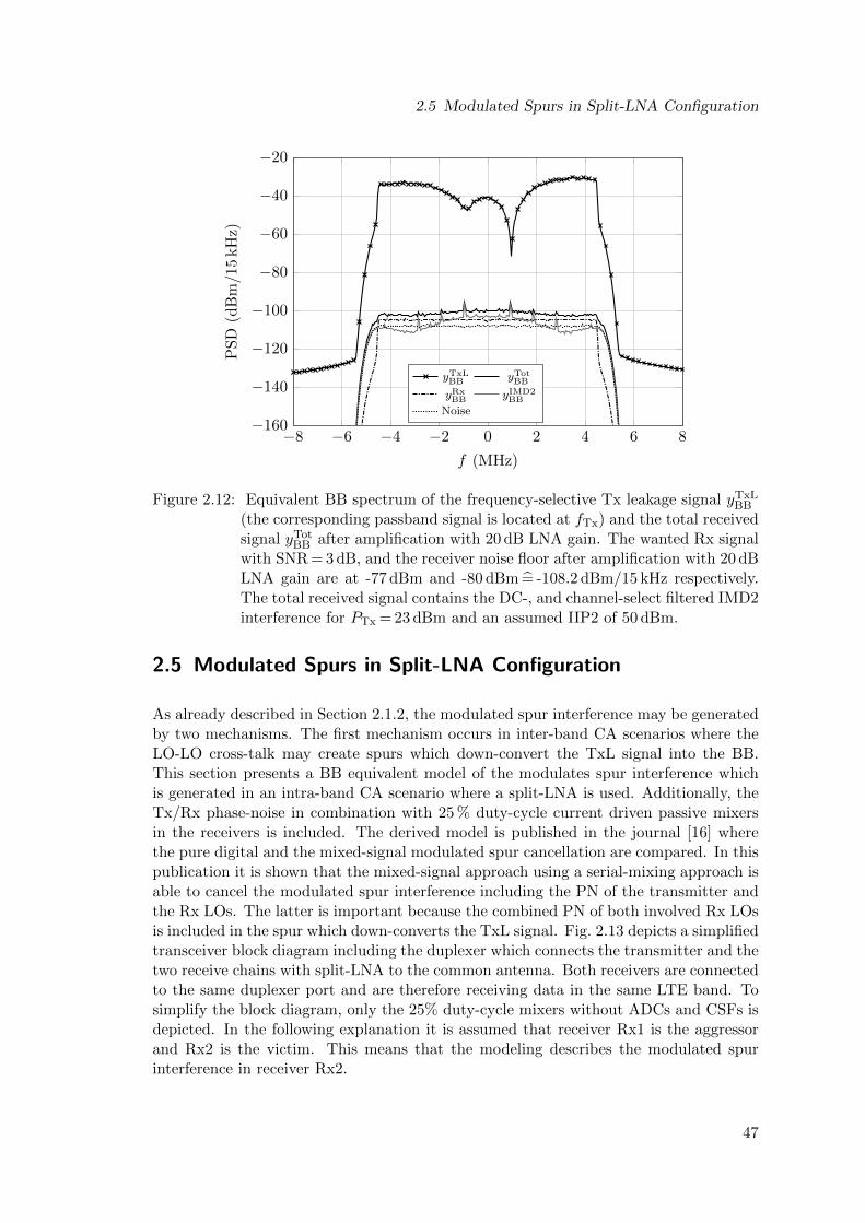
2.5 Modulated Spurs in Split-LNA Configuration
−8 −6 −4 −2 0 2 4 6 8−160
−140
−120
−100
−80
−60
−40
−20
f (MHz)
PS
D(d
Bm
/15
kH
z)
yTxLBB yTot
BB
yRxBB yIMD2
BB
Noise
Figure 2.12: Equivalent BB spectrum of the frequency-selective Tx leakage signal yTxLBB
(the corresponding passband signal is located at fTx) and the total receivedsignal yTot
BB after amplification with 20 dB LNA gain. The wanted Rx signalwith SNR = 3 dB, and the receiver noise floor after amplification with 20 dBLNA gain are at -77 dBm and -80 dBm = -108.2 dBm/15 kHz respectively.The total received signal contains the DC-, and channel-select filtered IMD2interference for PTx = 23 dBm and an assumed IIP2 of 50 dBm.
2.5 Modulated Spurs in Split-LNA Configuration
As already described in Section 2.1.2, the modulated spur interference may be generatedby two mechanisms. The first mechanism occurs in inter-band CA scenarios where theLO-LO cross-talk may create spurs which down-convert the TxL signal into the BB.This section presents a BB equivalent model of the modulates spur interference whichis generated in an intra-band CA scenario where a split-LNA is used. Additionally, theTx/Rx phase-noise in combination with 25 % duty-cycle current driven passive mixersin the receivers is included. The derived model is published in the journal [16] wherethe pure digital and the mixed-signal modulated spur cancellation are compared. In thispublication it is shown that the mixed-signal approach using a serial-mixing approach isable to cancel the modulated spur interference including the PN of the transmitter andthe Rx LOs. The latter is important because the combined PN of both involved Rx LOsis included in the spur which down-converts the TxL signal. Fig. 2.13 depicts a simplifiedtransceiver block diagram including the duplexer which connects the transmitter and thetwo receive chains with split-LNA to the common antenna. Both receivers are connectedto the same duplexer port and are therefore receiving data in the same LTE band. Tosimplify the block diagram, only the 25% duty-cycle mixers without ADCs and CSFs isdepicted. In the following explanation it is assumed that receiver Rx1 is the aggressorand Rx2 is the victim. This means that the modeling describes the modulated spurinterference in receiver Rx2.
47
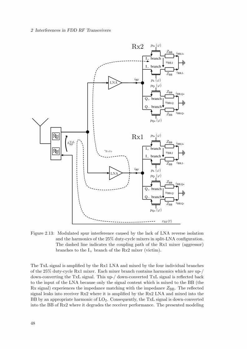
2 Interferences in FDD RF Transceivers
xRF(t)
hTxLRF
γI+I+
LNA
LNA
Rx1
Rx2
Figure 2.13: Modulated spur interference caused by the lack of LNA reverse isolationand the harmonics of the 25% duty-cycle mixers in split-LNA configuration.The dashed line indicates the coupling path of the Rx1 mixer (aggressor)branches to the I+ branch of the Rx2 mixer (victim).
The TxL signal is amplified by the Rx1 LNA and mixed by the four individual branchesof the 25% duty-cycle Rx1 mixer. Each mixer branch contains harmonics which are up-/down-converting the TxL signal. This up-/ down-converted TxL signal is reflected backto the input of the LNA because only the signal content which is mixed to the BB (theRx signal) experiences the impedance matching with the impedance ZBB. The reflectedsignal leaks into receiver Rx2 where it is amplified by the Rx2 LNA and mixed into theBB by an appropriate harmonic of LO2. Consequently, the TxL signal is down-convertedinto the BB of Rx2 where it degrades the receiver performance. The presented modeling
48
2.5 Modulated Spurs in Split-LNA Configuration
is carried out for 25 % duty-cycle mixers [29], although the derivation may be easilyadapted for 50 % duty-cycle mixers. The derived model shows, that the equivalent com-plex valued spur, which down-converts the TxL signal to the BB, has a gain-imbalancedue to the different coupling factors between each of the 8 mixer phases of the two 25%duty-cycle CA mixers. Consequently, the modulated spur interference consists of a mainand an image interference in the digital baseband.
2.5.1 Phase-Noise Model of the 25% Duty-Cycle Mixer
To be able to derive a mathematical model of the modulated spur, a detailed spur modelincluding the jitter in the pulse duration and variations in the LO period is needed. TheFourier coefficients ck of the 25 % duty-cycle mixer phase waveform pI+(t) (introducedin Section 2.2, Fig. 2.5) with amplitude A including the jitter 2δ in the pulse durationand the LO phase variation ϕLO are
ck =1
TLO
∫ TLO
0pI+(t)e−jk(2πfLOt+ϕLO)dt
=1
TLO
∫ TLO/4+δ
−δAe−jk(2πfLOt+ϕLO)dt
= A
[1
4+ 2
δ
TLO
]e−jk
π4 sinc
(kπ
4+ k2π
δ
TLO
)e−jkϕLO .
(2.86)
A detailed derivation of the Fourier coefficients ck including the PN may be found inAppendix A.2. Allowing slow variations of δ and ϕLO, the Fourier coefficients includingamplitude- and phase-noise may be expressed as
ck(t) = A
[1
4+ 2
δ(t)
TLO
]e−jk
π4 sinc
(kπ
4+ k2π
δ(t)
TLO
)e−jkϕLO(t). (2.87)
The resulting model of the I+ phase in the 25 % duty-cycle mixer including amplitude-,and phase-noise is
pI+(t) =∞∑
k=−∞ck(t)e
jk2πfLOt. (2.88)
The model for the I-,Q+ and Q- mixer phases of LO1 and LO2 are presented in Ap-pendix A.2.
2.5.2 Spur Modeling
In a CA receiver including two receivers in split-LNA configuration, the coupling andmixing between the I+ branch mixer waveform of aggressor LO1
pLO1,I+(t) =
∞∑
m1=−∞am1(t)ejm12πfLO1
t(2.89)
with the I+ branch mixer waveform of LO2 (victim)
pLO2,I+(t) =
∞∑
m2=−∞bm2(t)ejm22πfLO2
t(2.90)
49
2 Interferences in FDD RF Transceivers
corresponds to the equivalent spur psp,I+(t) = γI+I+ · pLO1,I+(t) · pLO2,I+(t) includingamplitude- and phase-noise in the I+ phase of LO2. Here γI+I+ is the coupling factorbetween the I+ phases of LO1 and LO2. As a particular example, the local oscillatorfundamental frequencies fLO1 = 1940 MHz and fLO2 = 1980 MHz are chosen. Throughthe coupling between the harmonics m1 = ±2 of LO1 and m2 = ±1 of LO2, the realvalued spur
psp,I+(t) = γI+I+
[a2(t)b∗1(t)ej2πfspt + a∗2(t)b1(t)e−j2πfspt
]
= 2 γI+I+a′2(t)b′1(t) · cos
(2πfspt− 2ϕLO1(t) + ϕLO2(t)− π
4
) (2.91)
with fsp = 2fLO1 − fLO2 = 1900 MHz is generated in the I+ phase of LO2. Here, the spurterms at the frequencies ± (2fLO1 + fLO2) are neglected. Similar spurs are generatedthrough the coupling between all other mixer phases (I-,Q+,Q-) of the two involved IQ-mixers (in Appendix A.2 all coupling paths are derived). Combining all spurs which aregenerated in the 16 coupling paths, an equivalent complex valued RF spur of the form
psp(t) = a∗2(t)b1(t)K1e−j2πfspt
+ a2(t)b∗1(t)K2ej2πfspt
(2.92)
is generated with K1 = (γI + γQ) /2 and K2 = (γI − γQ) /2 which down-converts anyblocker signal located near fsp into the Rx2 BB. Here γI and γQ are the resultingcoupling factors from LO1 to the I-, and Q-path of LO2, respectively. The modelingin Appendix A.2 shows that the spur can have a gain imbalance if γI and γQ are notidentical. In the literature, this is known as IQ-imbalance [15, 36, 37]. If the transmitfrequency fTx is close to the spur frequency fsp, the TxL signal is down-converted to thereceiver baseband resulting in a main and image interference which leads to a degradationof the desired receive signal.
2.5.3 Modulated Spur with IQ-Imbalance and Tx/Rx PN
The transmitter signal including phase-noise
xRF(t) = APA<xBB(t)ej(2πfTxt+ϕTx(t))
(2.93)
leaks through the frequency-selective duplexer stop-band, which is modeled by the im-pulse response hTxL
RF (t), into the receiver. Here APA is the power amplifier gain, the signalxBB(t) = xI(t) + jxQ(t) is the baseband transmit signal and ϕTx(t) the phase noise. Theresulting transmitter leakage signal is
yTxLRF (t) = xRF(t) ∗ hTxL
RF (t)
= APA<[xBB(t) ∗ hTxL
BB (t)]ej(2πfTxt+ϕTx(t))
,
(2.94)
and the total received signal at the output of the LNA with gain ALNA becomes
yTotRF,LNA(t) = ALNA
[yTxL
RF (t) + yRxRF(t) + vRF(t)
], (2.95)
including the desired receive signal yRxRF(t) and the noise vRF(t). The signal after the
mixeryTot
RF,mixer(t) = ALNA yTxLRF (t)psp(t)
+ALNA
[yRx
RF(t) + vRF(t)]e−j2πfLO1
t(2.96)
50
2.5 Modulated Spurs in Split-LNA Configuration
includes the desired receive signal, the noise, and the leakage signal which is down-converted by the noisy spur with IQ-imbalance. Here, the cross-modulation terms e.g.between the Rx signal and the spur, and the amplitude- and phase-noise in the down-conversion of the desired signal are neglected. By using the identity
<ηejκ
=
1
2
(ηejκ + η∗e−jκ
)(2.97)
and assuming an anti-aliasing filter in front of the ADC which attenuates the mixer prod-ucts in (2.96) which are outside the desired BB bandwidth, the total received discrete-time baseband signal becomes10
yTotBB [n] =
[n∑
l=−∞xsBB[l]hTot
BB [l, n− l] +K2
K∗1
n∑
l=−∞xs∗BB[l]hTot*
BB [l, n− l]]∗ hs[n]
︸ ︷︷ ︸=yMS
BB [n]...modulated spur interference (main + image)
+ALNA
2
[yRx
BB[n] + vBB[n]]∗ hs[n].
(2.98)
Here,
hTotBB [l, n] =
ALNAAPAK1
2
[ej(ϕTx[l]+2ϕLO1
[l]−ϕLO2[l]+π
4 ) · a′2[l]b′1[l]hTxLBB [n]e
j2πf∆fsn]
(2.99)is the time-variant BB equivalent Tx-to-Rx impulse response including the PN termsand
xsBB[n] =
[xBB[n]e
j2πf∆fsn]∗ hs[n], (2.100)
is a frequency shifted version of the transmit baseband signal with f∆ = fTx − fsp. Thefrequency fs denotes the sampling frequency and hs[n] is the impulse response of thecombined DC-cancellation and channel-select filter. The derived model shows, that themodulated spur interference consists of a main and an image component reasoned bythe gain imbalance of the spur. Furthermore, it can be observed in (2.99), that the jitter2δ in the pulse duration of the 25 % duty-cycle waveform leads to an amplitude noisein hTot
BB [n, l]. Whereas the PN of both LOs contribute to an equivalent PN of hTotBB [n, l].
Both individual effects are finally leading to a time-variant impulse response hTotBB [n, l]
which degrades the estimation of the impulse response by an adaptive filter and therebythe cancellation of the modulated spur interference.
The author of this thesis contributed this section to the journal [16]. There it is shownby the derived modulated spur model and also verified by using Matlab post-cancellationusing measured data that the pure digital modulated spur cancellation approach is notable to cancel the PN. However, in this journal a mixed-signal modulated spur cancel-lation concept is proposed. This approach mimics the spur generation mechanism byusing a serial-mixing approach where the real LO signals including their PN are used.The proposed solution is able to cancel the modulated spur interference including theTx and LO1/LO2 PN and therefore outperforms the pure digital approach.
10Due to the time-variant Tx-to-Rx impulse response hTotBB [n, l], the convolution in (2.47) changes to that
in (2.98).
51

3Interference Rejection
3.1 Introduction
As described in Section 2.2, the 25% duty-cycle current driven passive mixer is widelyused in modern RF receivers. It is preferably used in direct-conversion receivers andlow-voltage applications [29]. The RF output current iRF of the LNA flows into thefour switching branches of the passive mixer and creates a differential I and Q BB volt-age. Depending on the switching functions at the four transistor gates of the mixer, thepassive mixer has different properties. Traditional designs using 50 % duty-cycle gatecontrol signals suffer by an IQ cross-talk problem due to the overlapping ON-states ofthe switches in the I-, and Q-branch. The conversion gain is also reduced because theRF input current is divided into two branches [48]. To overcome this drawbacks, the25% duty-cycle control scheme was introduced which offers a 3 dB higher conversion gainand a reduced noise figure compared to the 50 % duty-cycle concept [29, 33].
A well known issue in square-wave mixers is the generation of harmonics in the mixerbranches [49, 50, 51] which lead to the down-conversion of unwanted spectral compo-nents contained in the RF input current iRF. This down-conversion by the so-calledharmonic response of the mixer may lead to a degradation of the wanted signal.
This chapter presents a novel HR strategy for 25% duty-cycle current-driven passivemixers. With this approach, the down-conversion of unwanted spectral content by themixer’s harmonic response may be significantly reduced.
Problem statement
Due to the design of wide-band analog front-ends in order to cover the high frequencyrange used in LTE, blocker signals may reach the mixer input. These blocker signals maybe down-converted to the Rx BB through the harmonic response of the mixer therebydegrading the wanted signal. Such a harmonic down-conversion for an LTE CA scenariowith two receivers and one transmitter is depicted in Fig. 3.1 (a). The carrier frequencyfLO1 of the PCC downlink receiver is coupled to the primary Tx frequency fTx by theduplexing distance. However, the carrier frequency fLO2 of the SCC receiver may belocated at any different frequency depending on intra/inter-band CA [3]. This may leadto the harmonic down-conversion of transmitter harmonics which leak through the du-plexer into the receiver. Assuming an LTE inter-band CA mode with the uplink PCCin band 11 at fTx = 1433 MHz, and the downlink SCC in band 8 at fLO2 = 955 MHz,the 2nd order Tx harmonic signal will be present at 2866 MHz. At the same time, the
53
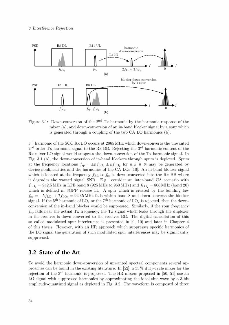
3 Interference Rejection
(a)
(b)
PSD B8 DL
fLO2
B11 UL
fTx 2fTx ≈ 3fLO2
Tx H2
harmonicdown-conversion
f f0
PSD B20 DL B8 DL
blocker down-conversionby a spur
fLO1fspfLO2
f f0
Figure 3.1: Down-conversion of the 2nd Tx harmonic by the harmonic response of themixer (a), and down-conversion of an in-band blocker signal by a spur whichis generated through a coupling of the two CA LO harmonics (b).
3rd harmonic of the SCC Rx LO occurs at 2865 MHz which down-converts the unwanted2nd order Tx harmonic signal to the Rx BB. Rejecting the 3rd harmonic content of theRx mixer LO signal would suppress the down-conversion of the Tx harmonic signal. InFig. 3.1 (b), the down-conversion of in-band blockers through spurs is depicted. Spursat the frequency locations fsp = ±nfLO1 ± kfLO2 for n, k ∈ N may be generated bydevice nonlinearities and the harmonics of the CA LOs [10]. An in-band blocker signalwhich is located at the frequency fBL ≈ fsp is down-converted into the Rx BB whereit degrades the wanted signal SNR. E.g. consider an inter-band CA scenario withfLO1 = 942.5 MHz in LTE band 8 (925 MHz to 960 MHz) and fLO2 = 806 MHz (band 20)which is defined in 3GPP release 11. A spur which is created by the building lawfsp = −5fLO1 + 7fLO2 = 929.5 MHz falls within band 8 and down-converts the blockersignal. If the 5th harmonic of LO1 or the 7th harmonic of LO2 is rejected, then the down-conversion of the in-band blocker would be suppressed. Similarly, if the spur frequencyfsp falls near the actual Tx frequency, the Tx signal which leaks through the duplexerin the receiver is down-converted to the receiver BB. The digital cancellation of thisso called modulated spur interference is presented in [9, 10] and later in Chapter 4of this thesis. However, with an HR approach which suppresses specific harmonics ofthe LO signal the generation of such modulated spur interferences may be significantlysuppressed.
3.2 State of the Art
To avoid the harmonic down-conversion of unwanted spectral components several ap-proaches can be found in the existing literature. In [52], a 33 % duty-cycle mixer for therejection of the 3rd harmonic is proposed. The HR mixers proposed in [50, 51] use anLO signal with suppressed harmonics by approximating the ideal sine wave by a 3-bitamplitude-quantized signal as depicted in Fig. 3.2. The waveform is composed of three
54
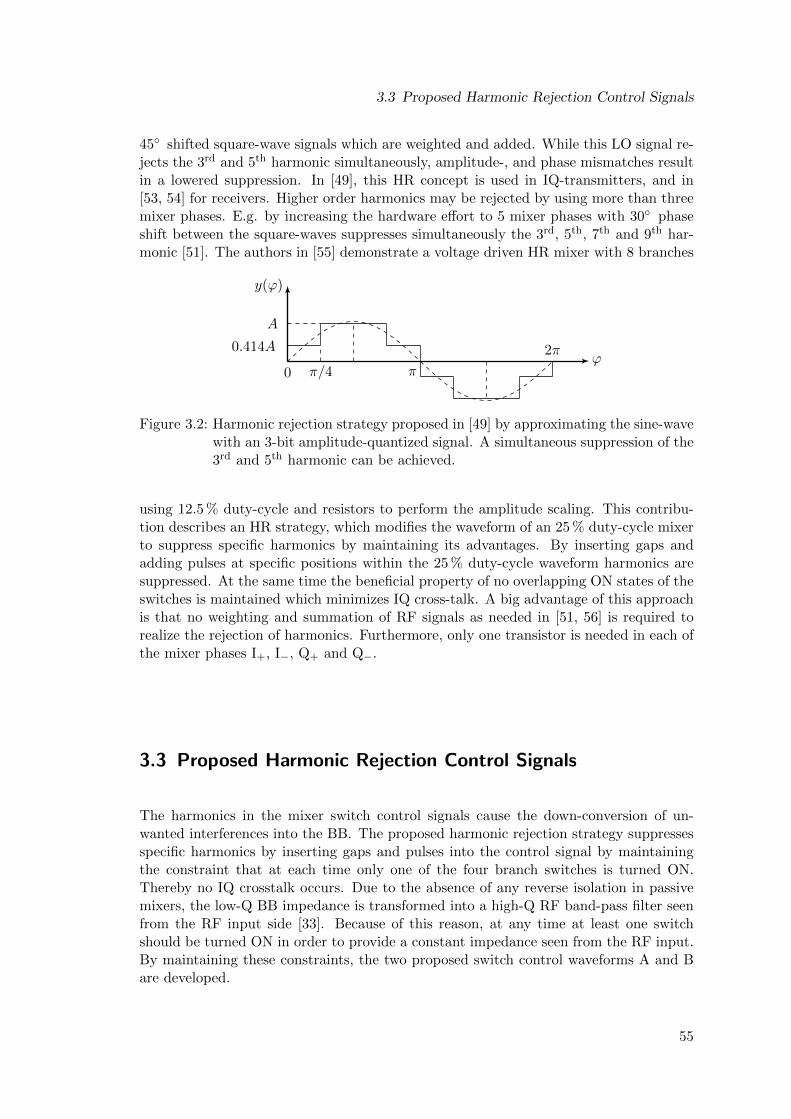
3.3 Proposed Harmonic Rejection Control Signals
45 shifted square-wave signals which are weighted and added. While this LO signal re-jects the 3rd and 5th harmonic simultaneously, amplitude-, and phase mismatches resultin a lowered suppression. In [49], this HR concept is used in IQ-transmitters, and in[53, 54] for receivers. Higher order harmonics may be rejected by using more than threemixer phases. E.g. by increasing the hardware effort to 5 mixer phases with 30 phaseshift between the square-waves suppresses simultaneously the 3rd, 5th, 7th and 9th har-monic [51]. The authors in [55] demonstrate a voltage driven HR mixer with 8 branches
ϕ
y(ϕ)
0 π
2π
π/4
A
0.414A
Figure 3.2: Harmonic rejection strategy proposed in [49] by approximating the sine-wavewith an 3-bit amplitude-quantized signal. A simultaneous suppression of the3rd and 5th harmonic can be achieved.
using 12.5 % duty-cycle and resistors to perform the amplitude scaling. This contribu-tion describes an HR strategy, which modifies the waveform of an 25 % duty-cycle mixerto suppress specific harmonics by maintaining its advantages. By inserting gaps andadding pulses at specific positions within the 25 % duty-cycle waveform harmonics aresuppressed. At the same time the beneficial property of no overlapping ON states of theswitches is maintained which minimizes IQ cross-talk. A big advantage of this approachis that no weighting and summation of RF signals as needed in [51, 56] is required torealize the rejection of harmonics. Furthermore, only one transistor is needed in each ofthe mixer phases I+, I−, Q+ and Q−.
3.3 Proposed Harmonic Rejection Control Signals
The harmonics in the mixer switch control signals cause the down-conversion of un-wanted interferences into the BB. The proposed harmonic rejection strategy suppressesspecific harmonics by inserting gaps and pulses into the control signal by maintainingthe constraint that at each time only one of the four branch switches is turned ON.Thereby no IQ crosstalk occurs. Due to the absence of any reverse isolation in passivemixers, the low-Q BB impedance is transformed into a high-Q RF band-pass filter seenfrom the RF input side [33]. Because of this reason, at any time at least one switchshould be turned ON in order to provide a constant impedance seen from the RF input.By maintaining these constraints, the two proposed switch control waveforms A and Bare developed.
55
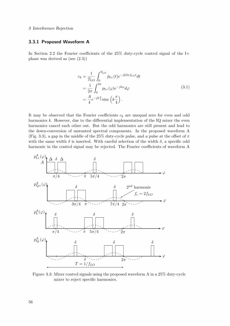
3 Interference Rejection
3.3.1 Proposed Waveform A
In Section 2.2 the Fourier coefficients of the 25% duty-cycle control signal of the I+phase was derived as (see (2.3))
ck =1
TLO
∫ TLO
0pI+(t)e−jk2πfLOtdt
=1
2π
∫ 2π
0pI+(ϕ)e−jkϕdϕ
=A
4e−jk
π4 sinc
(kπ
4
).
(3.1)
It may be observed that the Fourier coefficients ck are unequal zero for even and oddharmonics k. However, due to the differential implementation of the IQ mixer the evenharmonics cancel each other out. But the odd harmonics are still present and lead tothe down-conversion of unwanted spectral components. In the proposed waveform A(Fig. 3.3), a gap in the middle of the 25% duty-cycle pulse, and a pulse at the offset of πwith the same width δ is inserted. With careful selection of the width δ, a specific oddharmonic in the control signal may be rejected. The Fourier coefficients of waveform A
ϕ
pAI+(ϕ)
π/4
δδ
π 5π/4 2π
A∆ ∆
ϕ
pAQ+(ϕ)
3π/4
δδ
π 7π/4 2π
2nd harmonic
fc = 2fLO
ϕ
pAI-(ϕ)
5π/4
δ δδ
ππ/4 2π
ϕ
pAQ-(ϕ)
δ δδ
π 2πT = 1/fLO
Figure 3.3: Mixer control signals using the proposed waveform A in a 25% duty-cyclemixer to reject specific harmonics.
56
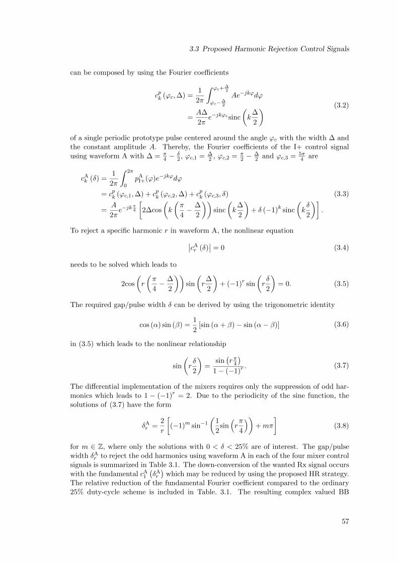
3.3 Proposed Harmonic Rejection Control Signals
can be composed by using the Fourier coefficients
cpk (ϕc,∆) =1
2π
∫ ϕc+∆2
ϕc−∆2
Ae−jkϕdϕ
=A∆
2πe−jkϕcsinc
(k
∆
2
) (3.2)
of a single periodic prototype pulse centered around the angle ϕc with the width ∆ andthe constant amplitude A. Thereby, the Fourier coefficients of the I+ control signalusing waveform A with ∆ = π
4 − δ2 , ϕc,1 = ∆
2 , ϕc,2 = π2 − ∆
2 and ϕc,3 = 5π4 are
cAk (δ) =
1
2π
∫ 2π
0pA
I+(ϕ)e−jkϕdϕ
= cpk (ϕc,1,∆) + cpk (ϕc,2,∆) + cpk (ϕc,3, δ)
=A
2πe−jk
π4
[2∆cos
(k
(π
4− ∆
2
))sinc
(k
∆
2
)+ δ (−1)k sinc
(kδ
2
)].
(3.3)
To reject a specific harmonic r in waveform A, the nonlinear equation
∣∣cAr (δ)
∣∣ = 0 (3.4)
needs to be solved which leads to
2cos
(r
(π
4− ∆
2
))sin
(r
∆
2
)+ (−1)r sin
(rδ
2
)= 0. (3.5)
The required gap/pulse width δ can be derived by using the trigonometric identity
cos (α) sin (β) =1
2[sin (α+ β)− sin (α− β)] (3.6)
in (3.5) which leads to the nonlinear relationship
sin
(rδ
2
)=
sin(r π4)
1− (−1)r. (3.7)
The differential implementation of the mixers requires only the suppression of odd har-monics which leads to 1 − (−1)r = 2. Due to the periodicity of the sine function, thesolutions of (3.7) have the form
δAr =
2
r
[(−1)m sin−1
(1
2sin(rπ
4
))+mπ
](3.8)
for m ∈ Z, where only the solutions with 0 < δ < 25% are of interest. The gap/pulsewidth δA
r to reject the odd harmonics using waveform A in each of the four mixer controlsignals is summarized in Table 3.1. The down-conversion of the wanted Rx signal occurswith the fundamental cA
1
(δAr
)which may be reduced by using the proposed HR strategy.
The relative reduction of the fundamental Fourier coefficient compared to the ordinary25% duty-cycle scheme is included in Table. 3.1. The resulting complex valued BB
57
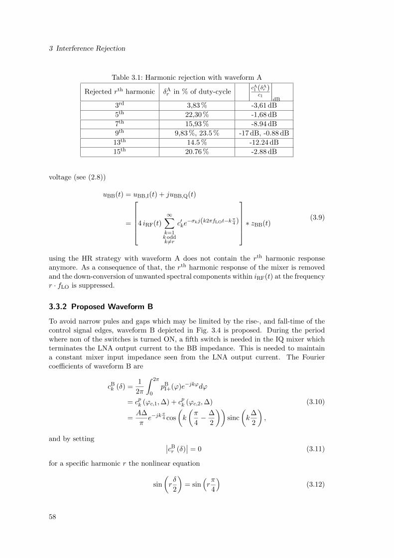
3 Interference Rejection
Table 3.1: Harmonic rejection with waveform A
Rejected rth harmonic δAr in % of duty-cycle
∣∣∣∣cA1 (δA
r )c1
∣∣∣∣dB
3rd 3,83 % -3,61 dB
5th 22,30 % -1,68 dB
7th 15,93 % -8.94 dB
9th 9,83 %, 23.5 % -17 dB, -0.88 dB
13th 14.5 % -12.24 dB
15th 20.76 % -2.88 dB
voltage (see (2.8))
uBB(t) = uBB,I(t) + juBB,Q(t)
=
4 iRF(t)
∞∑
k=1k oddk 6=r
c′ke−σkj(k2πfLOt−k π4 )
∗ zBB(t)
(3.9)
using the HR strategy with waveform A does not contain the rth harmonic responseanymore. As a consequence of that, the rth harmonic response of the mixer is removedand the down-conversion of unwanted spectral components within iRF(t) at the frequencyr · fLO is suppressed.
3.3.2 Proposed Waveform B
To avoid narrow pules and gaps which may be limited by the rise-, and fall-time of thecontrol signal edges, waveform B depicted in Fig. 3.4 is proposed. During the periodwhere non of the switches is turned ON, a fifth switch is needed in the IQ mixer whichterminates the LNA output current to the BB impedance. This is needed to maintaina constant mixer input impedance seen from the LNA output current. The Fouriercoefficients of waveform B are
cBk (δ) =
1
2π
∫ 2π
0pB
I+(ϕ)e−jkϕdϕ
= cpk (ϕc,1,∆) + cpk (ϕc,2,∆)
=A∆
πe−jk
π4 cos
(k
(π
4− ∆
2
))sinc
(k
∆
2
),
(3.10)
and by setting ∣∣cBr (δ)
∣∣ = 0 (3.11)
for a specific harmonic r the nonlinear equation
sin
(rδ
2
)= sin
(rπ
4
)(3.12)
58
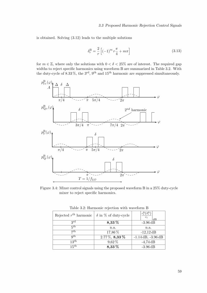
3.3 Proposed Harmonic Rejection Control Signals
is obtained. Solving (3.12) leads to the multiple solutions
δBr =
2
r
[(−1)m r
π
4+mπ
](3.13)
for m ∈ Z, where only the solutions with 0 < δ < 25% are of interest. The required gapwidths to reject specific harmonics using waveform B are summarized in Table 3.2. Withthe duty-cycle of 8.33 %, the 3rd, 9th and 15th harmonic are suppressed simultaneously.
ϕ
pBI+(ϕ)
π/4
δ
π 5π/4 2π
A∆ ∆
ϕ
pBQ+(ϕ)
3π/4
δ
π 7π/4 2π
2nd harmonic
ϕ
pBI-(ϕ)
5π/4
δ
ππ/4 2π
ϕ
pBQ-(ϕ)
δ
π 2πT = 1/fLO
Figure 3.4: Mixer control signals using the proposed waveform B in a 25% duty-cyclemixer to reject specific harmonics.
Table 3.2: Harmonic rejection with waveform B
Rejected rth harmonic δ in % of duty-cycle
∣∣∣∣cB1 (δB
r )c1
∣∣∣∣dB
3rd 8,33 % -3.96 dB
5th n.a. n.a.
7th 17,86 % -12,12 dB
9th 2.77 %, 8,33 % -1.14 dB, -3.96 dB
13th 9,62 % -4,74 dB
15th 8,33 % -3.96 dB
59
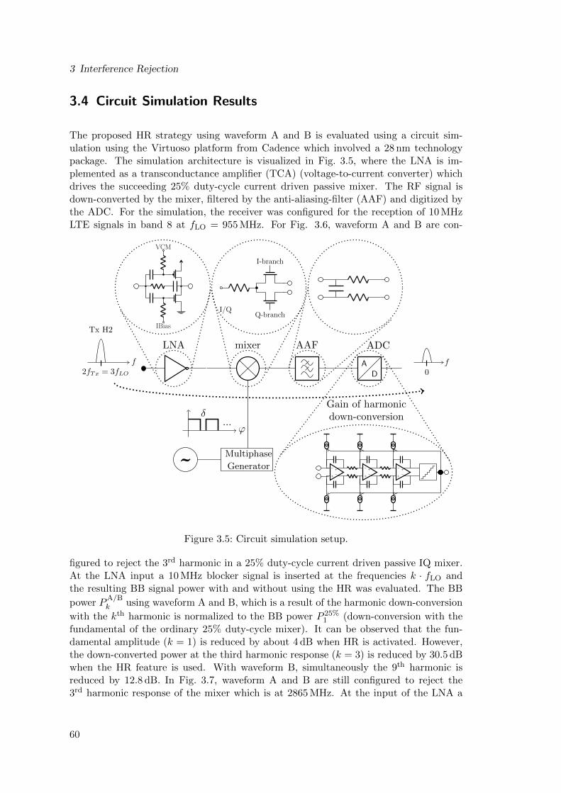
3 Interference Rejection
3.4 Circuit Simulation Results
The proposed HR strategy using waveform A and B is evaluated using a circuit sim-ulation using the Virtuoso platform from Cadence which involved a 28 nm technologypackage. The simulation architecture is visualized in Fig. 3.5, where the LNA is im-plemented as a transconductance amplifier (TCA) (voltage-to-current converter) whichdrives the succeeding 25% duty-cycle current driven passive mixer. The RF signal isdown-converted by the mixer, filtered by the anti-aliasing-filter (AAF) and digitized bythe ADC. For the simulation, the receiver was configured for the reception of 10 MHzLTE signals in band 8 at fLO = 955 MHz. For Fig. 3.6, waveform A and B are con-
AD
LNA mixer AAF ADC
IBias
VCM
I-branch
Q-branchI/Q
−
+−+
−
+−+
−
+−+
Multiphase
Generator˜
...δ
ϕ
Gain of harmonicdown-conversion
Tx H2
2fTx = 3fLO
f
0f
Figure 3.5: Circuit simulation setup.
figured to reject the 3rd harmonic in a 25% duty-cycle current driven passive IQ mixer.At the LNA input a 10 MHz blocker signal is inserted at the frequencies k · fLO andthe resulting BB signal power with and without using the HR was evaluated. The BB
power PA/Bk using waveform A and B, which is a result of the harmonic down-conversion
with the kth harmonic is normalized to the BB power P 25%1 (down-conversion with the
fundamental of the ordinary 25% duty-cycle mixer). It can be observed that the fun-damental amplitude (k = 1) is reduced by about 4 dB when HR is activated. However,the down-converted power at the third harmonic response (k = 3) is reduced by 30.5 dBwhen the HR feature is used. With waveform B, simultaneously the 9th harmonic isreduced by 12.8 dB. In Fig. 3.7, waveform A and B are still configured to reject the3rd harmonic response of the mixer which is at 2865 MHz. At the input of the LNA a
60
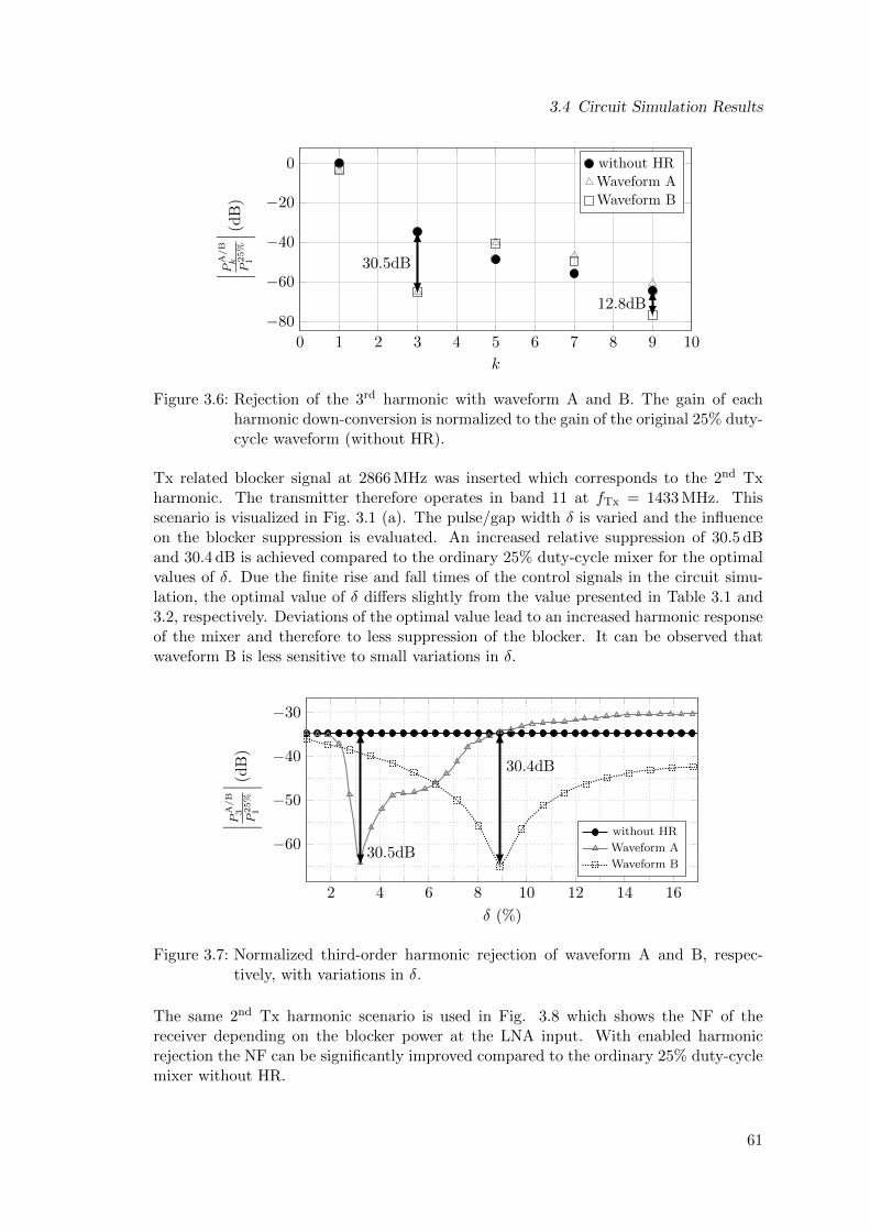
3.4 Circuit Simulation Results
0 1 2 3 4 5 6 7 8 9 10
−80
−60
−40
−20
0
k
∣ ∣ ∣ ∣PA
/B
k
P25%
1
∣ ∣ ∣ ∣(d
B)
without HR
Waveform A
Waveform B
30.5dB
12.8dB
Figure 3.6: Rejection of the 3rd harmonic with waveform A and B. The gain of eachharmonic down-conversion is normalized to the gain of the original 25% duty-cycle waveform (without HR).
Tx related blocker signal at 2866 MHz was inserted which corresponds to the 2nd Txharmonic. The transmitter therefore operates in band 11 at fTx = 1433 MHz. Thisscenario is visualized in Fig. 3.1 (a). The pulse/gap width δ is varied and the influenceon the blocker suppression is evaluated. An increased relative suppression of 30.5 dBand 30.4 dB is achieved compared to the ordinary 25% duty-cycle mixer for the optimalvalues of δ. Due the finite rise and fall times of the control signals in the circuit simu-lation, the optimal value of δ differs slightly from the value presented in Table 3.1 and3.2, respectively. Deviations of the optimal value lead to an increased harmonic responseof the mixer and therefore to less suppression of the blocker. It can be observed thatwaveform B is less sensitive to small variations in δ.
2 4 6 8 10 12 14 16
−60
−50
−40
−30
δ (%)
∣ ∣ ∣ ∣PA
/B
3
P25%
1
∣ ∣ ∣ ∣(d
B)
without HR
Waveform A
Waveform B30.5dB
30.4dB
Figure 3.7: Normalized third-order harmonic rejection of waveform A and B, respec-tively, with variations in δ.
The same 2nd Tx harmonic scenario is used in Fig. 3.8 which shows the NF of thereceiver depending on the blocker power at the LNA input. With enabled harmonicrejection the NF can be significantly improved compared to the ordinary 25% duty-cyclemixer without HR.
61
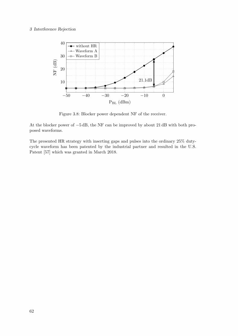
3 Interference Rejection
−50 −40 −30 −20 −10 0
10
20
30
40
PBL (dBm)
NF
(dB
)
without HR
Waveform A
Waveform B
21.1dB
Figure 3.8: Blocker power dependent NF of the receiver.
At the blocker power of −5 dB, the NF can be improved by about 21 dB with both pro-posed waveforms.
The presented HR strategy with inserting gaps and pulses into the ordinary 25% duty-cycle waveform has been patented by the industrial partner and resulted in the U.S.Patent [57] which was granted in March 2018.
62
4Adaptive Interference Cancellation
4.1 Introduction
This chapter deals with the digital cancellation of the modulated spur interference byadaptive filtering. As a starting point, adaptive filtering in the context of interferencecancellation using BB equivalent complex valued signals and systems is introduced inSection 4.2. Motivated by that, the Wirtinger derivatives [24, 58] will be recapitulatedin Section 4.3 which are used in the derivation of the complex valued LMS,- and RLSalgorithms in Section 4.4 and Section 4.5, respectively. As derived in Chapter 2, themodulated spur interference may be generated by LO-to-LO crosstalk in inter-band CAscenarios, or by the use of a split-LNA in intra-band CA scenarios. The main noveltyof this chapter is the derivation of a widely-linear [58] adaptive filter structure in Sec-tion 4.6 which is applicable for both cases. An additional contribution of this chapteris the performance evaluation of four adaptive filter algorithms for modulated spur can-cellation with respect to their convergence1 time and steady-state performance. At thetime when this PhD work has started no literature regarding the pure digital cancella-tion of the modulated spur interference was available. The modeling of the modulatedspur interference, and the performance evaluation of the algorithms have been presentedin [9] and [10].
4.2 Basic Adaptive Filter Structure
An adaptive filter is a self-adjusting filter, with a dedicated algorithm to update the filtercoefficients, to be able to react to changes of the unknown environment. The impulseresponse of an unknown system may change due to environmental influences. In thecontext of adaptive interference cancellation in RF transceivers, the unknown system isthe Tx-to-Rx transmitter leakage channel which may change over time due to tempera-ture drifts and/or a time varying antenna impedance mismatch. This leakage channel ismainly determined by the duplexer Tx-to-Rx stop-band frequency response which maybe heavily frequency-selective. In contrast to system identification applications wherethe impulse response of the unknown system is estimated, interference cancellation appli-cations focus on the estimation (or more precisely reconstruction) of the output signal ofthe unknown system. In the RF transceiver context, the estimated/reconstructed signalis the BB receiver interference caused by the TxL signal. This means that the receiver
1Gradient-based adaptive filters converge only in the mean because the noise influences the gradient.Consequently, when the filter reaches its steady state, the coefficients fluctuate around their optimalvalues [58].
63
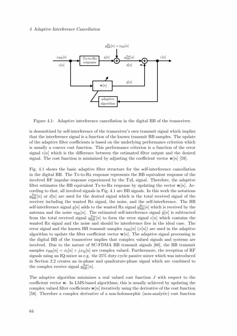
4 Adaptive Interference Cancellation
-xBB[n]
x[n]
yRxBB[n] + vBB[n]
yTotBB [n]
d[n]
y[n]
y[n]w[n]
Tx-to-Rxresponse
adaptive
algorithm
e[n]
Figure 4.1: Adaptive interference cancellation in the digital BB of the transceiver.
is desensitized by self-interference of the transceiver’s own transmit signal which impliesthat the interference signal is a function of the known transmit BB samples. The updateof the adaptive filter coefficients is based on the underlying performance criterion whichis usually a convex cost function. This performance criterion is a function of the errorsignal e[n] which is the difference between the estimated filter output and the desiredsignal. The cost function is minimized by adjusting the coefficient vector w[n] [59].
Fig. 4.1 shows the basic adaptive filter structure for the self-interference cancellationin the digital BB. The Tx-to-Rx response represents the BB equivalent response of theinvolved RF impulse response experienced by the TxL signal. Therefore, the adaptivefilter estimates the BB equivalent Tx-to-Rx response by updating the vector w[n]. Ac-cording to that, all involved signals in Fig. 4.1 are BB signals. In this work the notationsyTot
BB [n] or d[n] are used for the desired signal which is the total received signal of thereceiver including the wanted Rx signal, the noise, and the self-interference. The BBself-interference signal y[n] adds to the wanted Rx signal yRx
BB[n] which is received by theantenna and the noise vBB[n]. The estimated self-interference signal y[n] is subtractedfrom the total received signal yTot
BB [n] to form the error signal e[n] which contains thewanted Rx signal and the noise and should be interference free in the ideal case. Theerror signal and the known BB transmit samples xBB[n] (x[n]) are used in the adaptivealgorithm to update the filter coefficient vector w[n]. The adaptive signal processing inthe digital BB of the transceiver implies that complex valued signals and systems areinvolved. Due to the nature of SC-FDMA BB transmit signals [60], the BB transmitsamples xBB[n] = xI[n] + jxQ[n] are complex valued. Furthermore, the reception of RFsignals using an IQ-mixer as e.g. the 25% duty-cycle passive mixer which was introducedin Section 2.2 creates an in-phase and quadrature-phase signal which are combined tothe complex receive signal yTot
BB [n].
The adaptive algorithm minimizes a real valued cost function J with respect to thecoefficient vector w. In LMS-based algorithms, this is usually achieved by updating thecomplex valued filter coefficients w[n] iteratively using the derivative of the cost function[58]. Therefore a complex derivative of a non-holomorphic (non-analytic) cost function
64

4.3 Complex Derivatives
is needed. For this special case, the Cauchy-Riemann equations are not fulfilled andconsequently the traditional complex differentiation is not applicable. Because of thisreason, the Wirtinger Calculus [58] is discussed in Section 4.3 which introduces gener-alized complex derivatives of non-holomorphic cost functions, which exist whenever thecost function is real-differentiable.
4.3 Complex Derivatives
4.3.1 The Cauchy-Riemann Equations
The standard approach for complex differentiation is based on the Cauchy-Riemannequations. Let
f(w) = fr + jfi (4.1)
be a complex valued function f : CM → C. The function f can be interpreted as afunction g : R2M → R2 where the first coordinate represents the real part and thesecond the imaginary part of f :
f = fr + jfi → g =
[frfi
](4.2)
The function f is complex differentiable in the standard sense if and only if g is totallyreal differentiable and the Cauchy-Riemann equations
∂fr(wr,wi)
∂wr=∂fi(wr,wi)
∂wi
∂fi(wr,wi)
∂wr= −∂fr(wr,wi)
∂wi
(4.3)
hold [58]. If a function f on an open domain is complex-differentiable for every w in thedomain it is called holomorphic (analytic).
4.3.2 Adaptive Learning Algorithms
In statistical signal processing, a suitable objective (cost) function J(w) which is a func-tion of the coefficient vector w is either numerically or analytically minimized. For realvalued adaptive filters, this optimization problem is easily understood. The minimiza-tion may be done by updating the length M coefficient vector w[n] by e.g. the stochasticgradient algorithm [61]
w[n] = w[n− 1]− µ∇wJ [n], (4.4)
where
J(w)[n] = e2[n] (4.5)
is the real valued cost function J : RM 7→ R, and ∇wJ [n] the gradient with real valuedelements. However, as discussed in Section 4.2, adaptive filtering in the equivalent BBrequires the minimization of a cost function J : CM 7→ R because the BB equivalentsignals and systems are in general complex valued. This type of cost function is not
65

4 Adaptive Interference Cancellation
complex differentiable in the standard sense because the partial derivatives
∂Ji(wr,wi)
∂wi= 0
∂Ji(wr,wi)
∂wr= 0
both vanish and therefore the Cauchy-Riemann equations (4.3) do not apply. Conse-quently, to be able to derive adaptive learning algorithms which operate in the equivalentBB, a different way to derive an update equation as in (4.4) has to be found.
4.3.3 Wirtinger Derivatives
We will now discuss the differential change of g and f , respectively which gives mo-tivations for the definition of the gradient of f as well as for the so-called Wirtingerderivatives. The Jacobian matrix of g becomes
∇wg =
[∂fr∂wr
∂fr∂wi
∂fi∂wr
∂fi∂wi
], (4.6)
and the differential change of the function due to a change of the coefficients becomes
dg =
[dfrdfi
]=
[∂fr∂wr
∂fr∂wi
∂fi∂wr
∂fi∂wi
] [dwr
dwi
]. (4.7)
Switching back to the complex valued function, this leads to
df = dfr + jdfi =∂fr∂wr
dwr +∂fr∂wi
dwi + j∂fi∂wr
dwr + j∂fi∂wi
dwi, (4.8)
and with the variable swap
dwr =1
2[dw + dw∗]
dwi =1
2j[dw − dw∗]
(4.9)
we obtain
df(wr,wi) =∂fr∂wr
1
2[dw + dw∗] +
∂fr∂wi
1
2j[dw − dw∗] + j
∂fi∂wr
1
2[dw + dw∗]
+ j∂fi∂wi
1
2j[dw − dw∗]
=1
2
[∂fr∂wr
+ j∂fi∂wr
− j(∂fr∂wi
+ j∂fi∂wi
)]dw
+1
2
[∂fr∂wr
+ j∂fi∂wr
+ j
(∂fr∂wi
+ j∂fi∂wi
)]dw∗
=1
2
[∂f
∂wr− j ∂f
∂wi
]dw +
1
2
[∂f
∂wr+ j
∂f
∂wi
]dw∗.
(4.10)
66
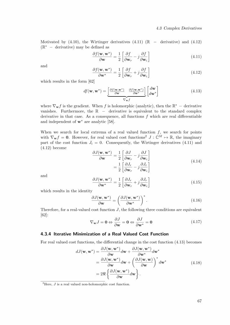
4.3 Complex Derivatives
Motivated by (4.10), the Wirtinger derivatives (4.11) (R − derivative) and (4.12)(R∗ − derivative) may be defined as
∂f(w,w∗)
∂w=
1
2
[∂f
∂wr− j ∂f
∂wi
](4.11)
and∂f(w,w∗)
∂w∗=
1
2
[∂f
∂wr+ j
∂f
∂wi
](4.12)
which results in the form [62]
df(w,w∗) =[∂f(w,w∗)
∂w∂f(w,w∗)∂w∗
]
︸ ︷︷ ︸∇wf
[dwdw∗
](4.13)
where ∇wf is the gradient. When f is holomorphic (analytic), then the R∗ − derivativevanishes. Furthermore, the R − derivative is equivalent to the standard complexderivative in that case. As a consequence, all functions f which are real differentiableand independent of w∗ are analytic [58].
When we search for local extrema of a real valued function f , we search for pointswith ∇wf = 0. However, for real valued cost functions2 J : CM 7→ R, the imaginarypart of the cost function Ji = 0. Consequently, the Wirtinger derivatives (4.11) and(4.12) become
∂J(w,w∗)
∂w=
1
2
[∂J
∂wr− j ∂J
∂wi
]
=1
2
[∂Jr∂wr
− j ∂Jr∂wi
] (4.14)
and∂J(w,w∗)
∂w∗=
1
2
[∂Jr∂wr
+ j∂Jr∂wi
](4.15)
which results in the identity
∂J(w,w∗)
∂w=
(∂J(w,w∗)
∂w∗
)∗. (4.16)
Therefore, for a real-valued cost function J , the following three conditions are equivalent[62]:
∇wJ = 0⇔ ∂J
∂w= 0⇔ ∂J
∂w∗= 0 (4.17)
4.3.4 Iterative Minimization of a Real Valued Cost Function
For real valued cost functions, the differential change in the cost function (4.13) becomes
dJ(w,w∗) =∂J(w,w∗)
∂wdw +
∂J(w,w∗)
∂w∗dw∗
=∂J(w,w∗)
∂wdw +
(∂J(w,w)
∂w
)∗dw∗
= 2<∂J(w,w∗)
∂wdw
.
(4.18)
2Here, J is a real valued non-holomorphic cost function.
67

4 Adaptive Interference Cancellation
In case of an iterative minimization of the cost function J , we seek for the greatestreduction dJ(w,w∗) between consecutive iterations. The maximum real valued changedJ(w,w∗) is given when the scalar product in the last line of (4.18) is maximized. This
is achieved when dw is a scaled version of[∂J(w,w∗)
∂w
]∗and therefore of ∂J(w,w∗)
∂w∗ [58, 63]
having in mind that J(w,w∗) is real valued. To get the highest sensitivity of changesin the cost function it is therefore favorable to move towards the R∗ − derivative (4.15)such that the coefficient update for the stochastic gradient algorithm using the WirtingerCalculus becomes [24, 58, 64, 65]
w[n] = w[n− 1]− 2µ
[∂J(w,w∗)
∂w∗
]T. (4.19)
4.4 The Least-Mean-Squares Algorithm
The traditional LMS algorithm may be derived from the Wiener solution [59, 61] byminimizing the mean-square-error (MSE) cost function
J (w,w∗) = E|e[n]|2
= E dd∗ − EdxH
w∗ − E
d∗xT
w + wTE
xxH
w∗
= σ2d − rTw∗ − rHw + wTRxxw∗
(4.20)
where d[n] is the desired signal, x[n] = [x[n], x[n− 1], . . . , x[n−M + 1]]T the delay-lineinput signal vector, w the length M coefficient vector, e[n] = d[n] − xT [n]w the error,r = E dx∗ is the cross-correlation vector and Rxx = E
xxH
the autocorrelation
matrix. The obtained cost function is dependent on w∗ and therefore not analytic.Using the Wirtinger derivative, we get
[∂J
∂w∗
]T= −
(r−RT
xxw), (4.21)
and setting the derivative to zero results in the Wiener solution
w =(RT
xx
)−1r. (4.22)
The optimal coefficient vector may also be obtained iteratively by the steepest descentmethod
w[n] = w[n− 1]− 2µ
[∂J
∂w∗
]T
= w[n− 1] + 2µ(r−RT
xxw[n− 1]).
(4.23)
The LMS algorithm operates iteratively on a sample basis by approximating the cross-correlation vector and autocorrelation matrix by their instantaneous estimates. Theapproximations r ≈ d[n]x∗[n] and RT
xx ≈ x∗[n]xT [n], lead to the LMS algorithm
w[n] = w[n− 1]− 2µ(d[n] + xT [n]w[n− 1]
)x∗[n]
= w[n− 1] + 2µe[n]x∗[n](4.24)
68
4.4 The Least-Mean-Squares Algorithm
where e[n] = d[n]− y[n] is the error between the desired signal d[n] and the estimatedsignal y[n] = xT [n]w[n− 1], and µ the step-size. The same result is obtained if theinstantaneous cost function
J (w,w∗) = |e[n]|2
= d[n]d∗[n]− d[n]xH [n]w∗[n− 1]− d∗[n]xT [n]w[n− 1] + wT [n− 1]x[n]xH [n]w∗[n− 1](4.25)
is minimized iteratively. Using the Wirtinger Calculus we get[
∂J
∂w∗[n− 1]
]T=(−d[n]xH [n] + wT [n− 1]x[n]xH [n]
)T
= −e[n]x∗[n],
(4.26)
which leads to the LMS coefficient update
w[n] = w[n− 1]− 2µ
[∂J
∂w∗[n− 1]
]T
= w[n− 1] + 2µe[n]x∗[n].
(4.27)
The Normalized Least-Mean-Squares Algorithm
Normalization improves the convergence speed3 of adaptive learning algorithms andprovides step-size bounds to maintain stability of the algorithm. In the following, twonormalization methods for the LMS algorithm are demonstrated:
Lets assume that the desired response is generated by d[n] = xT [n]w0 + q[n], whereq[n] is complex white Gaussian noise with zero mean and w0 the optimal coefficientvector. The coefficient error vector v[n] = w[n]−w0
v[n] = v[n− 1]− 2µx∗[n]x[n]v[n− 1] + 2µq[n]x∗[n] (4.28)
can be derived by inserting e[n] = d[n]−xT [n]w[n−1] in (4.27) and subtracting w0 fromboth sides [58]. Applying the statistical expectation operator on both sides of (4.28) andassuming that q[n] and x∗[n] are statistically independent we obtain
E v[n] = (I− 2µE x∗[n]x[n])E v[n− 1]=(I− 2µRT
xx
)E v[n− 1]
(4.29)
which leads to the step-size bounds [58]
0 < µ <1
trace (Rxx)=
1
ME|x[n]|2
≤ 1
λmax. (4.30)
Here, λmax is the maximum eigenvalue of the autocorrelation matrix Rxx, M the lengthof the coefficient vector w and x[n] the input signal. Incorporating this result for thestep-size bounds into the LMS algorithm (4.27), we obtain the normalized coefficientupdate
w[n] = w[n− 1] +µ0e[n]x∗[n]
ME|x[n]|2
(4.31)
3With convergence speed, the speed of error reduction in the mean square sense is meant.
69

4 Adaptive Interference Cancellation
with the step-size bounds 0 < µ0 < 2.
The second normalization approach can be used for linear and nonlinear adaptive al-gorithms and is based on [66]. In LMS-based algorithms, the a priori error signale[n] = d[n] − xT [n]w[n − 1] is used to update the filter coefficients. Step-size boundsto maintain convergence of the LMS algorithm (4.27) may be derived by analyzing therelationship between the errors e[n] and e[n+ 1]. For that we expand the instantaneouserror by a first order Taylor series expansion. However, as in [66] we use only the ex-pansion of the error with respect to the weight vector which is the driving term of thealgorithm. The first order Taylor series expansion results in
e[n+ 1] ≈ e[n] +∂e[n]
∂w[n− 1]∆w[n], (4.32)
where ∆w[n] = 2µe[n]x∗[n]. It has to be pointed out that the term e[n] is analytic(holomorphic) and therefore the standard complex derivative with respect to w[n− 1] isused to derive the first-order derivative (see page 9 in [67]). The first-order Taylor seriesexpansion therefore becomes4
e[n+ 1] ≈(1− 2µxH [n]x[n]
)e[n]. (4.33)
To maintain convergence [66] of the adaptive filter, the condition
∣∣1− 2µxH [n]x[n]∣∣ < 1 (4.34)
has to be fulfilled. To guarantee the condition (4.34), two cases have to be considered:
1. 1− 2µxH [n]x[n] < 1
which leads to µ > 0 and
2. 1− 2µxH [n]x[n] > −1
which results in µ < 1xH [n]x[n]
.
Combining both limits gives
0 < µ <1
xH [n]x[n](4.35)
which can be seen as a sample based approximation of (4.30). Including the factor2 in (4.27) into the step-size limits, the final normalized least-mean-squares (ε-NLMS)algorithm [61] with the regularization parameter ε becomes Algorithm 1. The smallpositive-valued real regularization parameter ε is used to prevent possible instabilitieswhen |x[n]|22 is very small and may be chosen as e.g. ε = 0.001.
4Here, the identity xT [n]x∗[n] = xH [n]x[n] is used.
70
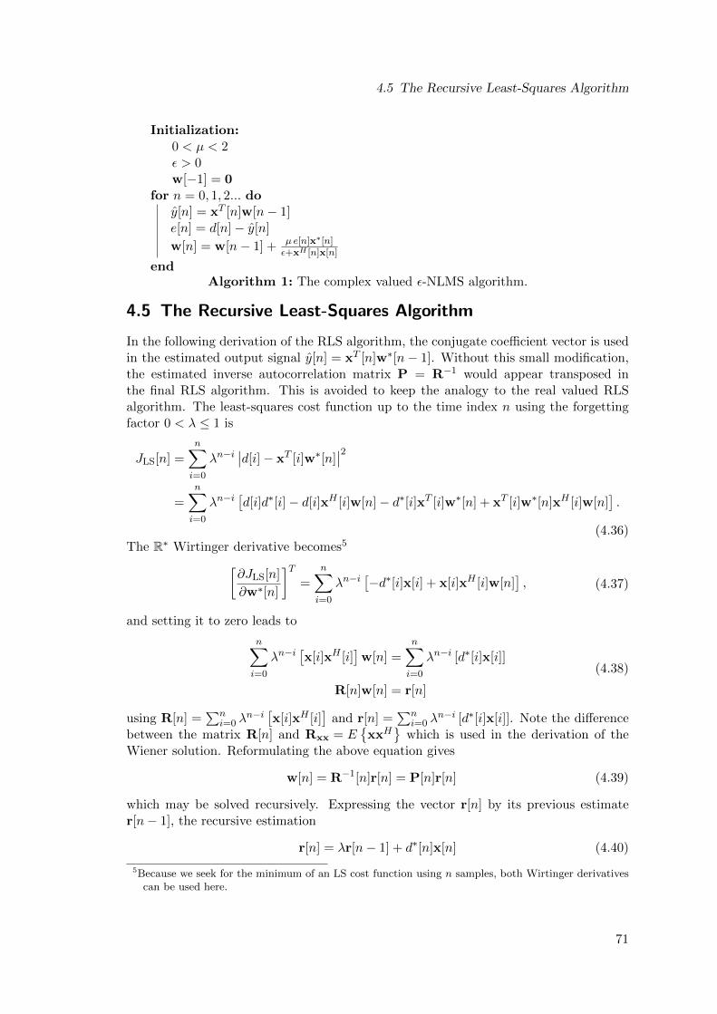
4.5 The Recursive Least-Squares Algorithm
Initialization:0 < µ < 2ε > 0w[−1] = 0
for n = 0, 1, 2... doy[n] = xT [n]w[n− 1]e[n] = d[n]− y[n]
w[n] = w[n− 1] + µ e[n]x∗[n]ε+xH [n]x[n]
endAlgorithm 1: The complex valued ε-NLMS algorithm.
4.5 The Recursive Least-Squares Algorithm
In the following derivation of the RLS algorithm, the conjugate coefficient vector is usedin the estimated output signal y[n] = xT [n]w∗[n− 1]. Without this small modification,the estimated inverse autocorrelation matrix P = R−1 would appear transposed inthe final RLS algorithm. This is avoided to keep the analogy to the real valued RLSalgorithm. The least-squares cost function up to the time index n using the forgettingfactor 0 < λ ≤ 1 is
JLS[n] =n∑
i=0
λn−i∣∣d[i]− xT [i]w∗[n]
∣∣2
=n∑
i=0
λn−i[d[i]d∗[i]− d[i]xH [i]w[n]− d∗[i]xT [i]w∗[n] + xT [i]w∗[n]xH [i]w[n]
].
(4.36)The R∗ Wirtinger derivative becomes5
[∂JLS[n]
∂w∗[n]
]T=
n∑
i=0
λn−i[−d∗[i]x[i] + x[i]xH [i]w[n]
], (4.37)
and setting it to zero leads to
n∑
i=0
λn−i[x[i]xH [i]
]w[n] =
n∑
i=0
λn−i [d∗[i]x[i]]
R[n]w[n] = r[n]
(4.38)
using R[n] =∑n
i=0 λn−i [x[i]xH [i]
]and r[n] =
∑ni=0 λ
n−i [d∗[i]x[i]]. Note the differencebetween the matrix R[n] and Rxx = E
xxH
which is used in the derivation of the
Wiener solution. Reformulating the above equation gives
w[n] = R−1[n]r[n] = P[n]r[n] (4.39)
which may be solved recursively. Expressing the vector r[n] by its previous estimater[n− 1], the recursive estimation
r[n] = λr[n− 1] + d∗[n]x[n] (4.40)
5Because we seek for the minimum of an LS cost function using n samples, both Wirtinger derivativescan be used here.
71
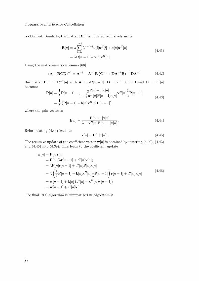
4 Adaptive Interference Cancellation
is obtained. Similarly, the matrix R[n] is updated recursively using
R[n] = λ
n−1∑
i=0
λn−i−1x[i]xH [i] + x[n]xH [n]
= λR[n− 1] + x[n]xH [n].
(4.41)
Using the matrix-inversion lemma [68]
(A + BCD)−1 = A−1 −A−1B(C−1 + DA−1B
)−1DA−1 (4.42)
the matrix P[n] = R−1[n] with A = λR[n − 1], B = x[n], C = 1 and D = xH [n]becomes
P[n] =1
λP[n− 1]−
1λP[n− 1]x[n]
1 + 1λxH [n]P[n− 1]x[n]
xH [n]1
λP[n− 1]
=1
λ
(P[n− 1]− k[n]xH [n]P[n− 1]
)(4.43)
where the gain vector is
k[n] =P[n− 1]x[n]
λ+ xH [n]P[n− 1]x[n]. (4.44)
Reformulating (4.44) leads tok[n] = P[n]x[n]. (4.45)
The recursive update of the coefficient vector w[n] is obtained by inserting (4.40), (4.43)and (4.45) into (4.39). This leads to the coefficient update
w[n] = P[n]r[n]
= P[n] (λr[n− 1] + d∗[n]x[n])
= λP[n]r[n− 1] + d∗[n]P[n]x[n]
= λ
(1
λP[n− 1]− k[n]xH [n]
1
λP[n− 1]
)r[n− 1] + d∗[n]k[n]
= w[n− 1] + k[n](d∗[n]− xH [n]w[n− 1]
)
= w[n− 1] + e∗[n]k[n].
(4.46)
The final RLS algorithm is summarized in Algorithm 2.
72
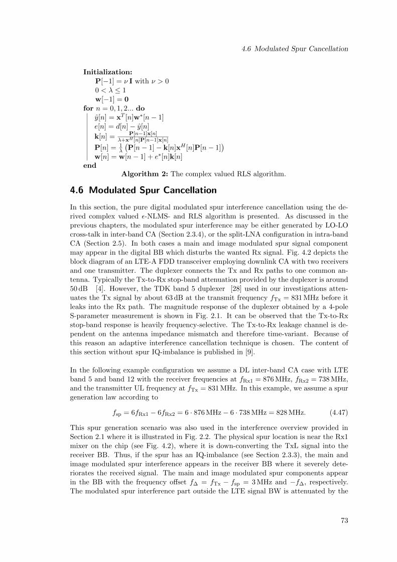
4.6 Modulated Spur Cancellation
Initialization:P[−1] = ν I with ν > 00 < λ ≤ 1w[−1] = 0
for n = 0, 1, 2... doy[n] = xT [n]w∗[n− 1]e[n] = d[n]− y[n]
k[n] = P[n−1]x[n]λ+xH [n]P[n−1]x[n]
P[n] = 1λ
(P[n− 1]− k[n]xH [n]P[n− 1]
)
w[n] = w[n− 1] + e∗[n]k[n]end
Algorithm 2: The complex valued RLS algorithm.
4.6 Modulated Spur Cancellation
In this section, the pure digital modulated spur interference cancellation using the de-rived complex valued ε-NLMS- and RLS algorithm is presented. As discussed in theprevious chapters, the modulated spur interference may be either generated by LO-LOcross-talk in inter-band CA (Section 2.3.4), or the split-LNA configuration in intra-bandCA (Section 2.5). In both cases a main and image modulated spur signal componentmay appear in the digital BB which disturbs the wanted Rx signal. Fig. 4.2 depicts theblock diagram of an LTE-A FDD transceiver employing downlink CA with two receiversand one transmitter. The duplexer connects the Tx and Rx paths to one common an-tenna. Typically the Tx-to-Rx stop-band attenuation provided by the duplexer is around50 dB [4]. However, the TDK band 5 duplexer [28] used in our investigations atten-uates the Tx signal by about 63 dB at the transmit frequency fTx = 831 MHz before itleaks into the Rx path. The magnitude response of the duplexer obtained by a 4-poleS-parameter measurement is shown in Fig. 2.1. It can be observed that the Tx-to-Rxstop-band response is heavily frequency-selective. The Tx-to-Rx leakage channel is de-pendent on the antenna impedance mismatch and therefore time-variant. Because ofthis reason an adaptive interference cancellation technique is chosen. The content ofthis section without spur IQ-imbalance is published in [9].
In the following example configuration we assume a DL inter-band CA case with LTEband 5 and band 12 with the receiver frequencies at fRx1 = 876 MHz, fRx2 = 738 MHz,and the transmitter UL frequency at fTx = 831 MHz. In this example, we assume a spurgeneration law according to
fsp = 6fRx1 − 6fRx2 = 6 · 876 MHz− 6 · 738 MHz = 828 MHz. (4.47)
This spur generation scenario was also used in the interference overview provided inSection 2.1 where it is illustrated in Fig. 2.2. The physical spur location is near the Rx1mixer on the chip (see Fig. 4.2), where it is down-converting the TxL signal into thereceiver BB. Thus, if the spur has an IQ-imbalance (see Section 2.3.3), the main andimage modulated spur interference appears in the receiver BB where it severely dete-riorates the received signal. The main and image modulated spur components appearin the BB with the frequency offset f∆ = fTx − fsp = 3 MHz and −f∆, respectively.The modulated spur interference part outside the LTE signal BW is attenuated by the
73
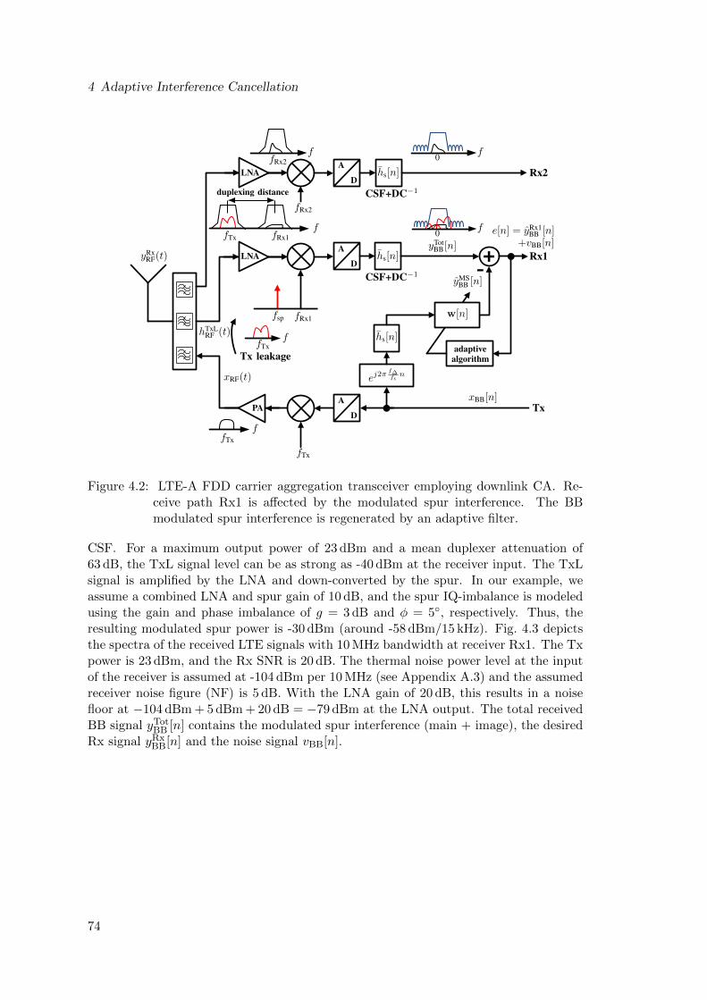
4 Adaptive Interference Cancellation
-
xBB[n]
e[n] = yRx1BB [n]
+vBB[n]
Rx2
Rx1
Tx
yTotBB[n]
yMSBB [n]
A
D
A
D
A
D
f
f
f
f f
f0
0fRx2
fsp fRx1
fRx2
hs[n]
hs[n]
hs[n]
CSF+DC−1
CSF+DC−1
LNA
LNA
fTx
yRxRF(t)
PA
fTx
fRx1
fTx
fTx
xRF(t)
hTxLRF (t)
ej2πf∆fsn
w[n]
adaptivealgorithmTx leakage
duplexing distance
Figure 4.2: LTE-A FDD carrier aggregation transceiver employing downlink CA. Re-ceive path Rx1 is affected by the modulated spur interference. The BBmodulated spur interference is regenerated by an adaptive filter.
CSF. For a maximum output power of 23 dBm and a mean duplexer attenuation of63 dB, the TxL signal level can be as strong as -40 dBm at the receiver input. The TxLsignal is amplified by the LNA and down-converted by the spur. In our example, weassume a combined LNA and spur gain of 10 dB, and the spur IQ-imbalance is modeledusing the gain and phase imbalance of g = 3 dB and φ = 5, respectively. Thus, theresulting modulated spur power is -30 dBm (around -58 dBm/15 kHz). Fig. 4.3 depictsthe spectra of the received LTE signals with 10 MHz bandwidth at receiver Rx1. The Txpower is 23 dBm, and the Rx SNR is 20 dB. The thermal noise power level at the inputof the receiver is assumed at -104 dBm per 10 MHz (see Appendix A.3) and the assumedreceiver noise figure (NF) is 5 dB. With the LNA gain of 20 dB, this results in a noisefloor at −104 dBm + 5 dBm + 20 dB = −79 dBm at the LNA output. The total receivedBB signal yTot
BB [n] contains the modulated spur interference (main + image), the desiredRx signal yRx
BB[n] and the noise signal vBB[n].
74
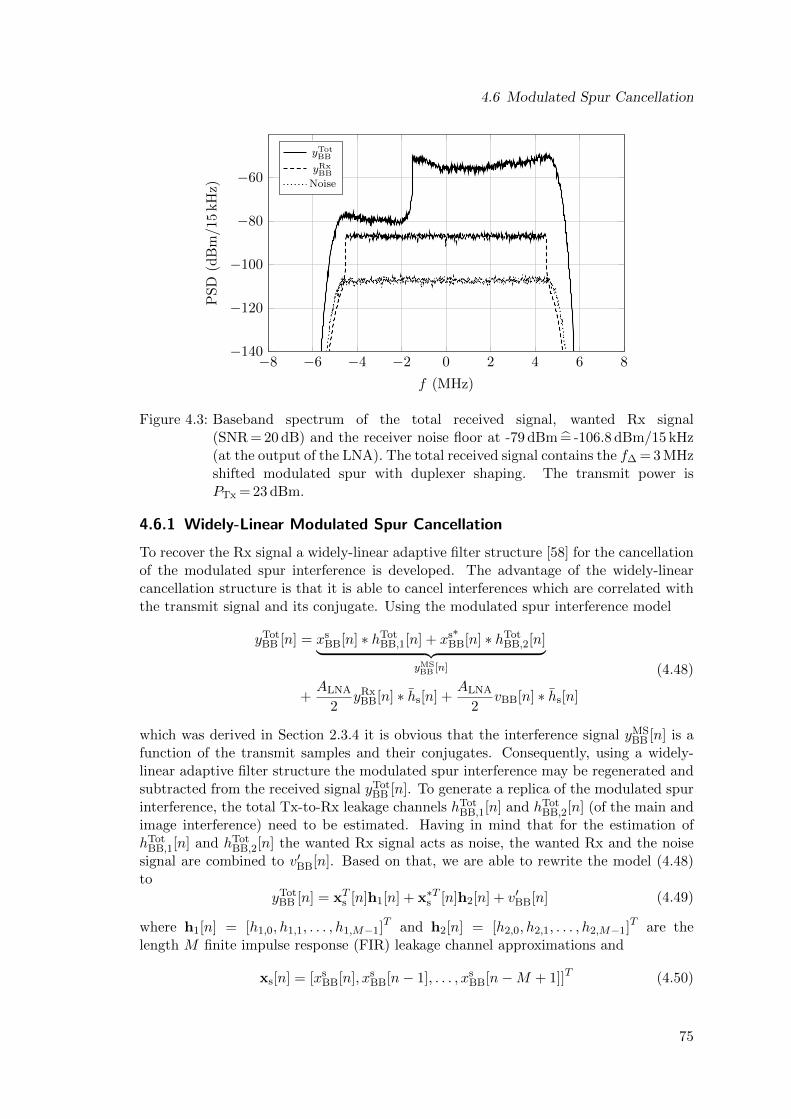
4.6 Modulated Spur Cancellation
−8 −6 −4 −2 0 2 4 6 8−140
−120
−100
−80
−60
f (MHz)
PS
D(d
Bm
/15
kH
z)
yTotBB
yRxBB
Noise
Figure 4.3: Baseband spectrum of the total received signal, wanted Rx signal(SNR = 20 dB) and the receiver noise floor at -79 dBm = -106.8 dBm/15 kHz(at the output of the LNA). The total received signal contains the f∆ = 3 MHzshifted modulated spur with duplexer shaping. The transmit power isPTx = 23 dBm.
4.6.1 Widely-Linear Modulated Spur Cancellation
To recover the Rx signal a widely-linear adaptive filter structure [58] for the cancellationof the modulated spur interference is developed. The advantage of the widely-linearcancellation structure is that it is able to cancel interferences which are correlated withthe transmit signal and its conjugate. Using the modulated spur interference model
yTotBB [n] = xs
BB[n] ∗ hTotBB,1[n] + xs*
BB[n] ∗ hTotBB,2[n]
︸ ︷︷ ︸yMSBB [n]
+ALNA
2yRx
BB[n] ∗ hs[n] +ALNA
2vBB[n] ∗ hs[n]
(4.48)
which was derived in Section 2.3.4 it is obvious that the interference signal yMSBB [n] is a
function of the transmit samples and their conjugates. Consequently, using a widely-linear adaptive filter structure the modulated spur interference may be regenerated andsubtracted from the received signal yTot
BB [n]. To generate a replica of the modulated spurinterference, the total Tx-to-Rx leakage channels hTot
BB,1[n] and hTotBB,2[n] (of the main and
image interference) need to be estimated. Having in mind that for the estimation ofhTot
BB,1[n] and hTotBB,2[n] the wanted Rx signal acts as noise, the wanted Rx and the noise
signal are combined to v′BB[n]. Based on that, we are able to rewrite the model (4.48)to
yTotBB [n] = xTs [n]h1[n] + x∗Ts [n]h2[n] + v′BB[n] (4.49)
where h1[n] = [h1,0, h1,1, . . . , h1,M−1]T and h2[n] = [h2,0, h2,1, . . . , h2,M−1]T are thelength M finite impulse response (FIR) leakage channel approximations and
xs[n] = [xsBB[n], xs
BB[n− 1], . . . , xsBB[n−M + 1]]T (4.50)
75
4 Adaptive Interference Cancellation
the delay-line input signal vector containing the frequency-shifted and channel-selectfiltered BB Tx samples
xsBB[n] =
[xBB[n]e
j2πf∆fsn]∗ hs[n]. (4.51)
Here, fs denotes the sampling frequency. The modulated spur interference is regeneratedby the widely-linear adaptive filter [58]
y[n] = xT [n]w[n− 1] (4.52)
where
w[n] =
[w1[n]w2[n]
](4.53)
and
x[n] =
[xs[n]x∗s [n]
](4.54)
is the augmented input signal vector containing the delay-line input signal vector xs[n]and its conjugate.
The performance of four adaptive algorithms to perform a modulated spur interfer-ence cancellation is compared. For this, the number of adaptive filter taps is set toM = 10 which corresponds to the length of the used Tx-to-Rx FIR leakage channel(duplexer) model. This means, the augmented adaptive filter to estimate the main andimage modulated spur interference has 2M = 20 taps. The ε-NLMS algorithm (Algo-rithm 1), the variable step-size normalized LMS (ε-VSSNLMS) algorithm, the regularizedaffine-projection algorithm (ε-APA), and the RLS algorithm (Algorithm 2) are evaluatedregarding convergence time and cancellation performance. The ε-NLMS-, and the RLS-algorithm are derived in Section 4.3, and a detailed description of the ε-APA algorithmmay be found in [61]. The proposed ε-VSSNLMS algorithm is an ε-NLMS variant withthe monotonically decreasing step-size
µ[n] =µ0
α · n+ β+ µmin. (4.55)
In this step-size update, µ0 sets the starting, and µmin the steady-state step-size value,respectively. With α and β the convergence rate can be adjusted, and stability is guar-anteed for 0 < µ[n] < 2. The modulated spur replica signal6
y[n] = xT [n]w[n− 1] (4.56)
is subtracted from the total received signal to form the error
e[n] = yTotBB [n]− y[n] (4.57)
which is used to employ an estimate of the leakage channel using the coefficient update
w[n] = w[n− 1] +µ[n]e[n]x∗[n]
ε+ xH [n]x[n]. (4.58)
6The RLS algorithm uses y[n] = xT [n]w∗[n− 1].
76
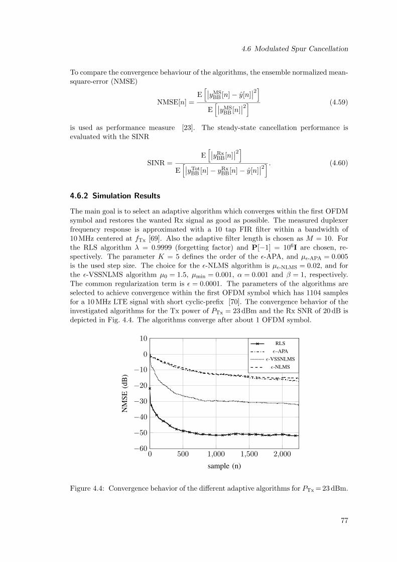
4.6 Modulated Spur Cancellation
To compare the convergence behaviour of the algorithms, the ensemble normalized mean-square-error (NMSE)
NMSE[n] =E[∣∣yMS
BB [n]− y[n]∣∣2]
E[∣∣yMS
BB [n]∣∣2] (4.59)
is used as performance measure [23]. The steady-state cancellation performance isevaluated with the SINR
SINR =E[∣∣yRx
BB[n]∣∣2]
E[∣∣yTot
BB [n]− yRxBB[n]− y[n]
∣∣2] . (4.60)
4.6.2 Simulation Results
The main goal is to select an adaptive algorithm which converges within the first OFDMsymbol and restores the wanted Rx signal as good as possible. The measured duplexerfrequency response is approximated with a 10 tap FIR filter within a bandwidth of10 MHz centered at fTx [69]. Also the adaptive filter length is chosen as M = 10. Forthe RLS algorithm λ = 0.9999 (forgetting factor) and P[−1] = 106I are chosen, re-spectively. The parameter K = 5 defines the order of the ε-APA, and µε-APA = 0.005is the used step size. The choice for the ε-NLMS algorithm is µε-NLMS = 0.02, and forthe ε-VSSNLMS algorithm µ0 = 1.5, µmin = 0.001, α = 0.001 and β = 1, respectively.The common regularization term is ε = 0.0001. The parameters of the algorithms areselected to achieve convergence within the first OFDM symbol which has 1104 samplesfor a 10 MHz LTE signal with short cyclic-prefix [70]. The convergence behavior of theinvestigated algorithms for the Tx power of PTx = 23 dBm and the Rx SNR of 20 dB isdepicted in Fig. 4.4. The algorithms converge after about 1 OFDM symbol.
0 500 1,000 1,500 2,000
10
0
−10
−20
−30
−40
−50
−60
sample (n)
NM
SE(d
B)
RLSε–APA
ε-VSSNLMSε-NLMS
Figure 4.4: Convergence behavior of the different adaptive algorithms for PTx = 23 dBm.
77
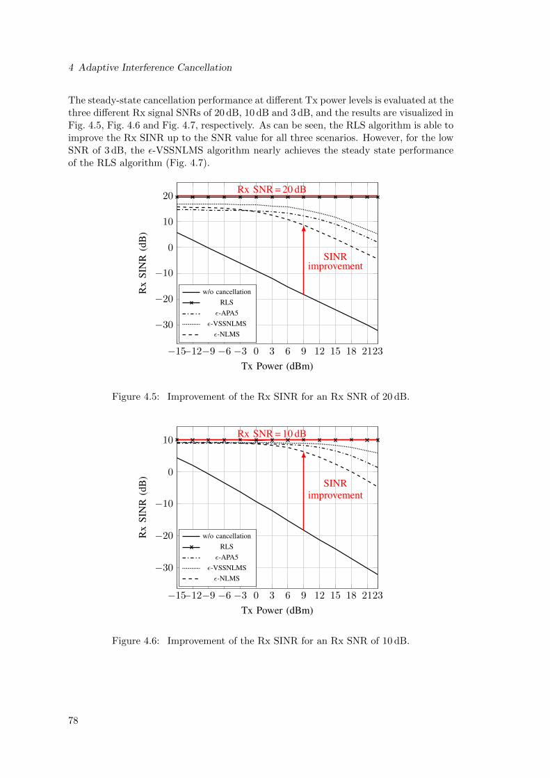
4 Adaptive Interference Cancellation
The steady-state cancellation performance at different Tx power levels is evaluated at thethree different Rx signal SNRs of 20 dB, 10 dB and 3 dB, and the results are visualized inFig. 4.5, Fig. 4.6 and Fig. 4.7, respectively. As can be seen, the RLS algorithm is able toimprove the Rx SINR up to the SNR value for all three scenarios. However, for the lowSNR of 3 dB, the ε-VSSNLMS algorithm nearly achieves the steady state performanceof the RLS algorithm (Fig. 4.7).
−15−12−9 −6 −3 0 3 6 9 12 15 18 2123
20
10
0
−10
−20
−30
SINRimprovement
Rx SNR = 20 dB
Tx Power (dBm)
Rx
SIN
R(d
B)
w/o cancellationRLS
ε-APA5ε-VSSNLMSε-NLMS
Figure 4.5: Improvement of the Rx SINR for an Rx SNR of 20 dB.
−15−12−9 −6 −3 0 3 6 9 12 15 18 2123
10
0
−10
−20
−30
SINRimprovement
Rx SNR = 10 dB
Tx Power (dBm)
Rx
SIN
R(d
B)
w/o cancellationRLS
ε-APA5ε-VSSNLMSε-NLMS
Figure 4.6: Improvement of the Rx SINR for an Rx SNR of 10 dB.
78
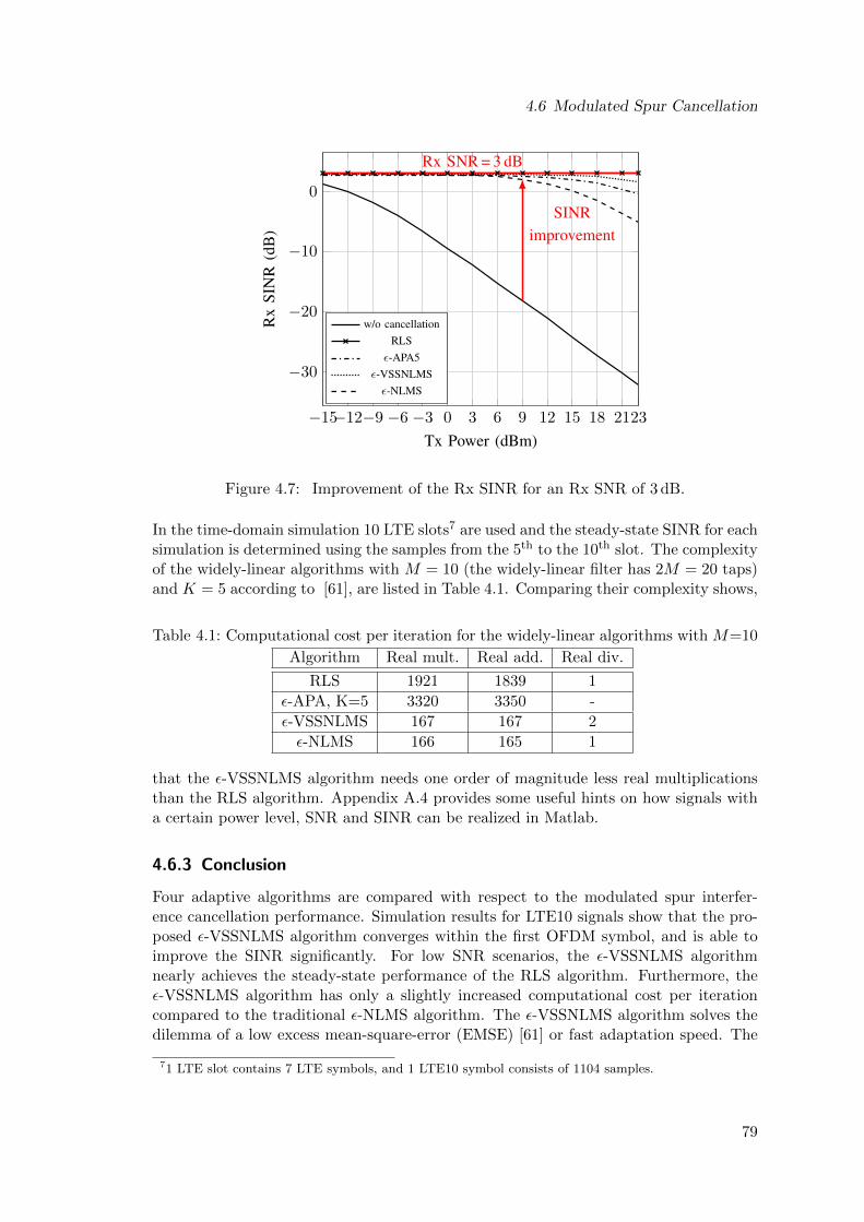
4.6 Modulated Spur Cancellation
−15−12−9 −6 −3 0 3 6 9 12 15 18 2123
0
−10
−20
−30
SINRimprovement
Rx SNR = 3 dB
Tx Power (dBm)
Rx
SIN
R(d
B)
w/o cancellationRLS
ε-APA5ε-VSSNLMSε-NLMS
Figure 4.7: Improvement of the Rx SINR for an Rx SNR of 3 dB.
In the time-domain simulation 10 LTE slots7 are used and the steady-state SINR for eachsimulation is determined using the samples from the 5th to the 10th slot. The complexityof the widely-linear algorithms with M = 10 (the widely-linear filter has 2M = 20 taps)and K = 5 according to [61], are listed in Table 4.1. Comparing their complexity shows,
Table 4.1: Computational cost per iteration for the widely-linear algorithms with M=10
Algorithm Real mult. Real add. Real div.
RLS 1921 1839 1
ε-APA, K=5 3320 3350 -
ε-VSSNLMS 167 167 2
ε-NLMS 166 165 1
that the ε-VSSNLMS algorithm needs one order of magnitude less real multiplicationsthan the RLS algorithm. Appendix A.4 provides some useful hints on how signals witha certain power level, SNR and SINR can be realized in Matlab.
4.6.3 Conclusion
Four adaptive algorithms are compared with respect to the modulated spur interfer-ence cancellation performance. Simulation results for LTE10 signals show that the pro-posed ε-VSSNLMS algorithm converges within the first OFDM symbol, and is able toimprove the SINR significantly. For low SNR scenarios, the ε-VSSNLMS algorithmnearly achieves the steady-state performance of the RLS algorithm. Furthermore, theε-VSSNLMS algorithm has only a slightly increased computational cost per iterationcompared to the traditional ε-NLMS algorithm. The ε-VSSNLMS algorithm solves thedilemma of a low excess mean-square-error (EMSE) [61] or fast adaptation speed. The
71 LTE slot contains 7 LTE symbols, and 1 LTE10 symbol consists of 1104 samples.
79

4 Adaptive Interference Cancellation
EMSE is connected to the MSE via
MSE = EMSE + E∣∣v′BB[n]
∣∣2, (4.61)
and for the ε-NLMS algorithm the EMSE may be approximated by [61]
EMSE =µE|v′BB[n]|2
2− µ . (4.62)
Consequently, for small values of the step-size µ, the MSE approaches the variance ofthe noise term v′BB[n] which includes the Rx signal and the noise.
80
5Adaptive IMD2 Cancellation
5.1 Introduction
This chapter is dedicated to the digital cancellation of the IMD2 interference by adap-tive filtering. For this purpose, a novel Wiener model [25] based nonlinear LMS-typealgorithm (IM2LMS), and a novel nonlinear RLS-type algorithm (IM2RLS) are derivedto cancel the IMD2 interference in the digital BB. Simulation results demonstrate thatthe proposed IM2LMS algorithms outperforms traditional Hammerstein-, and Volterramodel [25] based LMS algorithms in terms of convergence speed, steady-state perfor-mance and complexity. The proposed IM2LMS-, and IM2RLS algorithms are evaluatedusing measured IMD2 data which is obtained from two different measurement setups.The first setup includes a transceiver chip provided by the industrial partner, whereasthe second setup uses discrete RF components. The derivation and the performanceresults of the IM2LMS-, and the IM2RLS algorithm have been presented in [7] and [27],respectively.
An interesting fact of the nonlinear IMD2 interference is, that one part of the generatedsecond-order intermodulation products always falls around zero-frequency independentof the Tx-to-Rx frequency offset (duplexing distance). In case of direct-conversion re-ceiver architectures, this leads to a BB interference which disturbs the wanted receivesignal. The mathematical modeling in section 2.3.5 shows that the BB IMD2 inter-ference contains the squared envelope of the BB equivalent TxL signal. The resultingBB IMD2 interference has twice the Tx signal bandwidth and contains a DC due tothe envelope-squaring. The overall DC in the received signal is time-variant and mayhave many sources like e.g. LO-LO self mixing [8], and therefore must not be relatedexplicitly to the DC which is generated by the IMD2 interference. Direct-conversionreceivers employ a DC cancellation to suppress the DC in order to prevent the ADCfrom saturation. Consequently, the IMD2 interference related DC is removed from thereceived signal which complicates the IMD2 replica estimation. Furthermore, in thedigital domain the signal is filtered by a CSF to reduce its bandwidth to the LTE signalbandwidth. Thereby, parts of the IMD2 interference are filtered away. Consequently,the adaptive filter needs to generate an IMD2 interference replica without DC and withreduced bandwidth. Both effects complicate the replica generation by the adaptive filter.
Section 5.2 gives an overview about the state-of-the-art IMD2 interference cancellationapproaches. Section 5.3 describes how Hammerstein- and Volterra model based adap-tive filters may be used to estimate the nonlinear IMD2 interference. In Section 5.4,the Wiener model IM2LMS-, and the IM2RLS algorithms are derived. The performance
81
5 Adaptive IMD2 Cancellation
of the algorithms is compared by simulations and measured data in Section 5.5 andSection 5.6, respectively.
5.2 State of the Art
In the existing literature, the authors of [21, 22, 71] discussed an IMD2 cancellationconsisting of a Hammerstein model based LMS algorithm for frequency-flat duplexerstop-bands. In [23] a Volterra kernel based LS approach for frequency-selective Tx-to-Rx responses was proposed. The authors in [6] presented a two-step LS approachfor the IMD2 cancellation and considered a static 3rd-order PA nonlinearity and IQ-imbalance in the transmit mixer. In [72] a Tx CA transceiver was considered wherethe transmit signal of two transmitters leaks through a diplexer into one of the CAreceivers. The diplexer stop-band is modeled as a first-order FIR system which reflectsa nearly frequency-flat response. The authors incorporated a fourth-order nonlinearitywithout memory into the estimation process, which results in an LS problem with fourunknown coefficients. In the existing literature, the contributions [7, 23] considered theDC removal in the IMD2 interference replica, and in [6, 21, 22, 73] it is neglected. TheIMD2 interference in the receiver may also be generated by external blocker signalsreceived by the antenna. The author in [17, 18], extracts the blocker signal after the Rxmixer by a high-pass filter. The squared envelope of this signal is then used as a referencefor the subsequent adaptive filter which cancels the generated IMD2 interference.
5.3 Polynomial Filters
State-of-the-art nonlinear adaptive filtering is performed by discrete-time polynomialfilters [25] which are described with the input-output relationship
y[n] =P∑
i=0
fi (x[n], . . . , x[n−M + 1], y[n− 1], . . . , y[n−M + 1]) (5.1)
using the ith-order polynomial functions fi(·) and the polynomial order P . For theassumption of an underlying linear FIR system with the output relation
f1[n] =M−1∑
m=0
h1[m]x[n−m], (5.2)
the polynomial filter for P = 2 has the form [25]
y[n] = h0 +
M−1∑
m1=0
h1[m1]x[n−m1)
+
M−1∑
m1=0
M−1∑
m2=0
h2[m1,m2]x[n−m1]x[n−m2].
(5.3)
Here, h0, h1[m1] and h2[m1,m2] are the constant, the linear and the second-order systemcoefficients, respectively. Switching to complex valued signals and systems, the IMD2interference may be described by a polynomial filter which has the order i = 2 with
f2(ξ[n]) = ξ[n]ξ[n]∗ = |ξ[n]|2 , (5.4)
82
5.3 Polynomial Filters
therefore reducing the polynomial filter to the truncated Volterra filter without constantand linear term. With ξ[n] = xBB[n] ∗ hTxL
BB [n] the IMD2 interference term
yIMD2BB [n] = α2
A2LNAA
2PA
2︸ ︷︷ ︸η
∣∣xBB[n] ∗ hTxLBB [n]
∣∣2 ∗ hs[n](5.5)
derived in (2.58) is expanded to
yIMD2BB [n] = η
[(xBB[n] ∗ hTxL
BB [n])·(xBB[n] ∗ hTxL
BB [n])∗] ∗ hs[n]
= η
[M−1∑
m1=0
M−1∑
m2=0
hTxLBB [m1]hTxL*
BB [m2]xBB[n−m1]x∗BB[n−m2]
]∗ hs[n]
= η
[M−1∑
m1=0
M−1∑
m2=0
hTxLBB [m1,m2]xBB[n−m1]x∗BB[n−m2]
]∗ hs[n]
(5.6)
which shows the underlying truncated Volterra-kernel structure with the two dimen-sional impulse response hTxL
BB [m1,m2] of the IMD2 interference problem.
For the estimation of the IMD2 interference contained in (2.58), the wanted Rx signalacts as noise and is therefore combined with the noise signal to the noise term v′BB[n].Inserting (5.6) into the model of the total received signal (2.58) results in the truncatedVolterra-kernel model
yTotBB [n] = η
[M−1∑
m1=0
M−1∑
m2=0
hTxLBB [m1,m2]xBB[n−m1]x∗BB[n−m2]
]∗ hs[n] + v′BB[n] (5.7)
of the total received signal. The model (5.6) is the foundation for the Hammerstein-, andVolterra model based IMD2 interference cancellation which are presented in Section 5.3.1and Section 5.3.2, respectively.
5.3.1 Hammerstein Model
The IMD2 model (5.6) incorporates M2 coefficients to estimate one IMD2 interferencesample. To lower the computational complexity of this Volterra model based cancellationapproach, the authors in [73] derived a low-complexity cancellation structure. Setting theindexes m1 = m2 = m in (5.6) means neglecting the cross terms of the two dimensionalimpulse response hTxL
BB [m1,m2]. Therefore only the diagonal elements of hTxLBB [m1,m2]
are used. The resulting simplified model1 with reduced complexity becomes
yIMD2BB [n] = η
[M−1∑
m=0
hTxLBB [m,m] |xBB[n−m]|2
]∗ hs[n]
= hT x[n] ∗ hs[n],
(5.8)
where
h = η[h0h
∗0, h1h
∗1, . . . , hM−1h
∗M−1
]T (5.9)
1This low complexity model assumes a frequency-flat Tx-to-Rx response. This assumption is only validfor Tx signals with very narrow bandwidth.
83
5 Adaptive IMD2 Cancellation
and
x[n] =[|xBB[n]|2 , |xBB[n− 1]|2 , . . . , |xBB[n−M + 1]|2
]T. (5.10)
This Hammerstein model assumption is used in [22] to perform a digital IMD2 inter-ference cancellation. The envelope-squaring nonlinearity is applied to the BB transmitsamples before the signal is convoluted with the diagonal elements of the two-dimensionalleakage path impulse response which is mainly determined by the duplexer. Another in-teresting case is given if the duplexer is perfectly frequency flat in the Tx signal frequencyrange which implies that all duplexer impulse response coefficients except one are zero[21]. Even for narrowband Tx signals used e.g. in UMTS this only holds approximately,but in general for wide-band LTE signals this is not valid. However, assuming a fre-quency flat duplexer with the signal delay δTs where δ ≥ 0 is an integer number and Tsthe sampling time, the model (5.6) is equivalent to
yIMD2BB [n] =
(hδ |xBB[n− δ]|2
)∗ hs[n], (5.11)
with hδ = η hTxLBB [δ, δ] . By allowing a fractional signal delay (e.g. δ = 2.4), which can
be approximated by an LMS adaptive filter [22], (5.11) changes to
yIMD2BB [n] =
(h′T x[n]
)∗ hs[n]. (5.12)
In this approximation, the vector h′ accounts for the fractional delay. Interestingly,the structure of (5.12) is the same as in (5.8), although the underlying assumptions arefundamentally different. The adaptive IMD2 interference regeneration may be performedwith the ε-NLMS algorithm (Algorithm 1) where the interference replica generation
yAC[n] =(xT [n]w[n− 1]
)∗ hs[n] (5.13)
contains the channel-select-, and DC filtering, and the length M coefficient vector w[n].Using dAC[n] as the channel-select- and DC filtered total received signal, the error signal
eAC[n] = dAC[n]− yAC[n] (5.14)
is used for the adaptive coefficient update
w[n] = w[n− 1] +µeAC[n]x∗s [n]
ε+ xHs [n]xs[n](5.15)
to employ an estimate of the IMD2 interference. It has to be highlighted, that theconvolution of the adaptive filter output signal with hs[n] introduces a signal delay dueto the group delay of the CSF. This signal delay has to be taken into account in thecoefficient update equation (5.15) to achieve a time-alignment between the error signaleAC and the input signal vector. This is achieved by filtering the input signal with theCSF
xs[n] =(|xBB[n]|2 − σ2
x
)∗ hs[n]. (5.16)
The DC cancellation in the adaptive filter input signal (5.16) is achieved by subtractingthe expectation value
σ2x = E
|xBB[n]|2
(5.17)
84
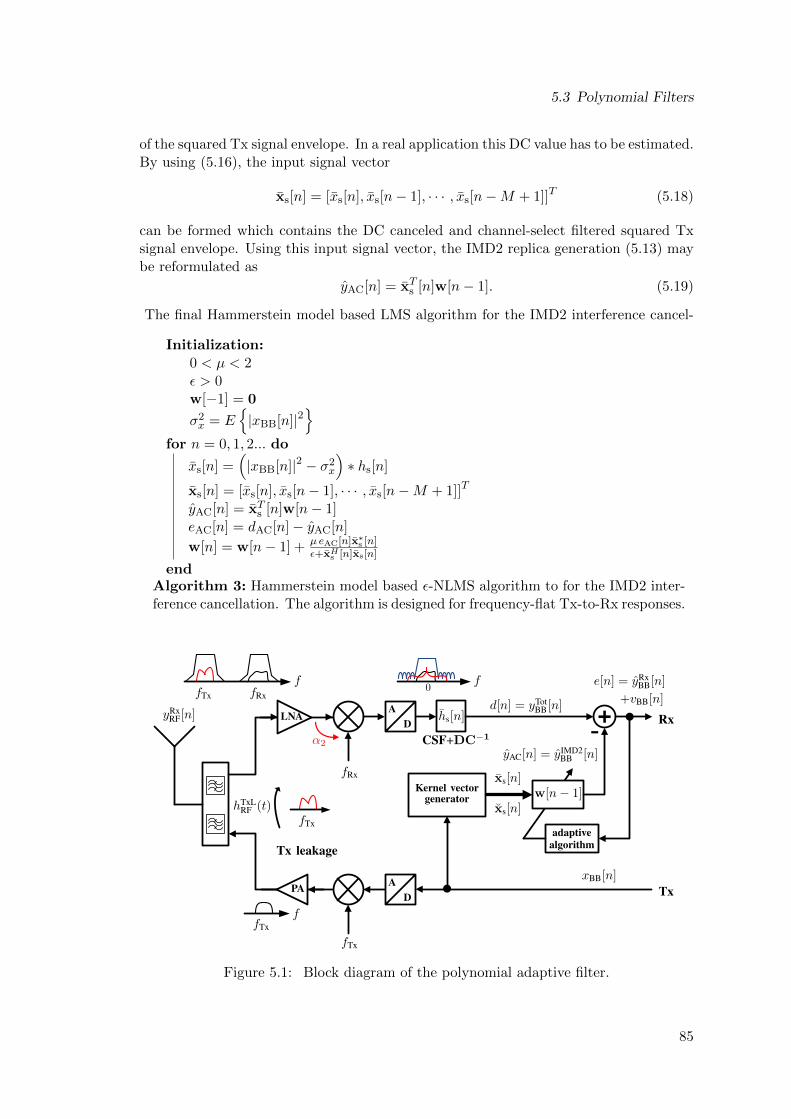
5.3 Polynomial Filters
of the squared Tx signal envelope. In a real application this DC value has to be estimated.By using (5.16), the input signal vector
xs[n] = [xs[n], xs[n− 1], · · · , xs[n−M + 1]]T (5.18)
can be formed which contains the DC canceled and channel-select filtered squared Txsignal envelope. Using this input signal vector, the IMD2 replica generation (5.13) maybe reformulated as
yAC[n] = xTs [n]w[n− 1]. (5.19)
The final Hammerstein model based LMS algorithm for the IMD2 interference cancel-
Initialization:0 < µ < 2ε > 0w[−1] = 0
σ2x = E
|xBB[n]|2
for n = 0, 1, 2... do
xs[n] =(|xBB[n]|2 − σ2
x
)∗ hs[n]
xs[n] = [xs[n], xs[n− 1], · · · , xs[n−M + 1]]T
yAC[n] = xTs [n]w[n− 1]eAC[n] = dAC[n]− yAC[n]
w[n] = w[n− 1] + µ eAC[n]x∗s [n]ε+xHs [n]xs[n]
endAlgorithm 3: Hammerstein model based ε-NLMS algorithm to for the IMD2 inter-ference cancellation. The algorithm is designed for frequency-flat Tx-to-Rx responses.
-
xBB[n]
yRxRF[n]
d[n] = yTotBB[n]
w[n− 1]xs[n]
Kernel vectorgenerator
xs[n]
yAC[n] = yIMD2BB [n]
e[n] = yRxBB[n]
+vBB[n]
LNA
PA
hs[n]
CSF+DC−1
hTxLRF (t)
AD
AD
adaptivealgorithmTx leakage
fTx
fTx
fTx
fTx
fRx
fRx
α2
f
f
0f
Rx
Tx
Figure 5.1: Block diagram of the polynomial adaptive filter.
85

5 Adaptive IMD2 Cancellation
lation is summarized in Algorithm 3. Fig. 5.1 shows the adaptive filter structure withthe kernel generator to form the nonlinear input signal vector xs[n].
5.3.2 Truncated Volterra Model
The IMD2 interference is a nonlinear interference including memory. This results fromthe fact that the Tx signal first leaks through the frequency-selective duplexer (whichintroduces a memory effect) and afterwards experiences the second-order nonlinearityof the mixer. By using the FIR Tx-to-Rx leakage channel approximation, the IMD2interference model (5.5) may be reformulated into a linear estimation problem [23].Approximating the duplexer by an FIR system of length M
hTxLBB [n] = [h0, h1, h2, . . . , hM−1]T , (5.20)
the model (5.6) may be rewritten to
yIMD2BB [n] =η
[M−1∑
m1=0
M−1∑
m2=0
hTxLBB [m1,m2]xBB[n−m1]x∗BB[n−m2]
]∗ hs[n]
=(hT [n]x[n]
)∗ hs[n]
(5.21)
which leads for e.g. M = 4 to the coefficient vector
h[n] = η [h0h∗0, h1h
∗1, h2h
∗2, h3h
∗3,
h0h∗1, h0h
∗2, h0h
∗3, h1h
∗2, h1h
∗3, h2h
∗3,
h1h∗0, h2h
∗0, h3h
∗0, h2h
∗1, h3h
∗1, h3h
∗2]T
(5.22)
and the corresponding Tx-kernel vector
x[n] = [xBB[n]x∗BB[n], xBB[n− 1]x∗BB[n− 1], xBB[n− 2]x∗BB[n− 2],
xBB[n− 3]x∗BB[n− 3], xBB[n]x∗BB[n− 1], xBB[n]x∗BB[n− 2],
xBB[n]x∗BB[n− 3], xBB[n− 1]x∗BB[x− 2], xBB[n− 1]x∗BB[n− 3],
xBB[n− 2]x∗BB[n− 3], xBB[n− 1]x∗BB[n], xBB[n− 2]x∗BB[n],
xBB[n− 3]x∗BB[n], xBB[n− 2]x∗BB[n− 1], xBB[n− 3]x∗BB[n− 1],
xBB[n− 3]x∗BB[n− 2]]T
(5.23)
with dimension M2. Both vectors have M real valued and M2−M complex entries. Byusing the identity
xBB[n]x∗BB[n− 1]h0h∗1 + xBB[n− 1]x∗BB[n]h1h
∗0 =
= 2 (<xBB[n]x∗BB[n− 1]<h0h∗1
−=xBB[n]x∗BB[n− 1]=h0h∗1) ,
(5.24)
the complex scalar-product in (5.21) may be rewritten as a scalar-product with the realvalued vectors
h′[n] = η [h0h∗0, h1h
∗1, h2h
∗2, h3h
∗3,
2<h0h∗1 , 2<h0h
∗2 , 2<h0h
∗3 , 2<h1h
∗2 , 2<h1h
∗3 ,
2<h2h∗3 , 2=h1h
∗0 , 2=h2h
∗0 , 2=h3h
∗0 ,
2=h2h∗1 , 2=h3h
∗1 , 2=h3h
∗2]T
(5.25)
86
5.3 Polynomial Filters
and
x′[n] = [xBB[n]x∗BB[n], xBB[n− 1]x∗BB[n− 1], xBB[n− 2]x∗BB[n− 2],
xBB[n− 3]x∗BB[n− 3],<xBB[n]x∗BB[n− 1] ,<xBB[n]x∗BB[n− 2] ,<xBB[n]x∗BB[n− 3] ,<xBB[n− 1]x∗BB[x− 2] ,<xBB[n− 1]x∗BB[n− 3] ,<xBB[n− 2]x∗BB[n− 3] ,=xBB[n]x∗BB[n− 1] ,=xBB[n]x∗BB[n− 2] ,=xBB[n]x∗BB[n− 3] ,=xBB[n− 1]x∗BB[n− 2] ,=xBB[n− 1]x∗BB[n− 3] ,=xBB[n− 2]x∗BB[n− 3]]T
(5.26)
where the minus sign of the imaginary part in (5.24) is included into the coefficients tobe estimated. For the estimation of the IMD2 interference with the normalized LMSalgorithm, the replica
yAC[n] =(x′T [n]w[n− 1]
)∗ hs[n] (5.27)
is used to generate the error signal
eAC[n] = dAC[n]− yAC[n] (5.28)
which is needed for the coefficient update
w[n] = w[n− 1] +µeAC[n]x′∗s [n]
ε+ x′Hs [n]x′s[n]. (5.29)
Also in the Volterra kernel based LMS update equation the signal delay introduced bythe convolution with the filter hs[n] in (5.27) has to be considered. This may be doneby introducing the new input signal vector
xs[n] =[|x[n]|2 − σ2
x, |x[n− 1]|2 − σ2x, |x[n− 2]|2 − σ2
x,
|x[n− 3]|2 − σ2x,<x[n]x[n− 1]∗ ,<x[n]x[n− 2]∗ ,
<x[n]x[n− 3]∗ ,<x[n− 1]x[x− 2]∗ ,<x[n− 1]x[n− 3]∗ ,<x[n− 2]x[n− 3]∗ ,=x[n]x[n− 1]∗ ,=x[n]x[n− 2]∗ ,=x[n]x[n− 3]∗ ,=x[n− 1]x[n− 2]∗ ,=x[n− 1]x[n− 3]∗ ,=x[n− 2]x[n− 3]∗]T ∗ hs[n]
(5.30)
which includes an implicit DC cancellation and the channel-select filtering. Unfortu-nately, in the Volterra LMS case the input signal vector is not a delay-line vector.Consequently, each of the M2 entries of the vector xs[n] needs to be filtered by hs[n]separately. This significantly increases the computational complexity of the Volterrakernel LMS algorithm. By using the new introduced input signal vector xs[n] whichincorporates the DC cancellation and the channel-select filtering, the replica generation(5.27) may be rewritten to
yAC[n] = xTs [n]w[n− 1]. (5.31)
The final Volterra kernel LMS algorithm is summarized in Algorithm 4 and the adaptivefilter structure is depicted in Fig. 5.1.
87

5 Adaptive IMD2 Cancellation
Initialization:0 < µ < 2ε > 0w[−1] = 0
for n = 0, 1, 2... doyAC[n] = xTs [n]w[n− 1]eAC[n] = dAC[n]− yAC[n]
w[n] = w[n− 1] + µ eAC[n]x∗s [n][n]ε+xHs [n]xs[n]
endAlgorithm 4: Volterra kernel based ε-NLMS algorithm for the IMD2 interferencecancellation with frequency-selective Tx-to-Rx responses.
88
5.4 Wiener Model Based Cancellation
5.4 Wiener Model Based Cancellation
In this section the nonlinear Wiener model is explored for the development of a nonlinearLMS/RLS type adaptive filter to estimate the IMD2 interference. The goal is to reducethe computational complexity of the Volterra kernel based adaptive filter described inSection 5.3.2. Especially for highly frequency-selective duplexer responses a large numberof FIR coefficients is required to model the Tx-to-Rx response. The Wiener model usesa static nonlinearity at the output of the adaptive filter which has the advantage thatless coefficients are necessary in the estimation process compared to a Volterra kernelbased adaptive filter [25]. In case of the IMD2 interference, this static nonlinearity isthe envelope-squaring operation and the Tx-to-Rx path is estimated by an underlyingFIR model.The following differences between the Wiener-, Hammerstein-, and Volterra models forthe adaptive IMD2 interference cancellation may be identified.
In LTE scenarios, the Tx-to-Rx leakage channel may be heavily frequency-selectivebecause of the duplexer stop-band. Therefore, the Hammerstein model whichassumes a frequency-flat leakage channel is not applicable. Consequently, the useof a Volterra-, or Wiener model based cancellation approach is necessary.
With increasing frequency-selectivity in general more FIR filter coefficients are nec-essary to model the leakage channel. The computational complexity of the Wienermodel adaptive filter increases with the order O(M), whereas the complexity ofthe Volterra model based cancellation increases by O(M2).
Due to the envelope-squaring at the output of the Wiener model, the IMD2 relatedDC is automatically regenerated in the interference replica signal. This DC needsto be removed afterwards because the main receiver employs a DC-cancellation.
The output signal of the Wiener filter using the envelope-squaring nonlinearity atthe output is always real valued. Reasoned by that, it is impossible to estimatethe complex valued IMD2 interference in the I-, and Q-path simultaneously withone combined adaptive filter.
However, the interference replica model described below will show that the Q-path IMD2interference is only a scaled version of the I-path interference. Therefore, once the I-pathIMD2 interference is estimated by the Wiener model adaptive filter, the I-path replicasignal may be used as a reference to estimate the Q-path IMD2 interference.
5.4.1 Interference Replica Model
For the adaptive filter development to cancel the IMD2 interference in the digital BB,the interference model (2.58) is rewritten to the form
yTotBB [n] =
αI2
2
∣∣ALNAAPAxBB[n] ∗ hTxLBB [n]
∣∣2 ∗ hs[n]︸ ︷︷ ︸
yIMD2,IBB [n]
+ jαQ
2
2
∣∣ALNAAPAxBB[n] ∗ hTxLBB [n]
∣∣2 ∗ hs[n]︸ ︷︷ ︸
yIMD2,QBB [n]
+v′BB[n]
(5.32)
89
5 Adaptive IMD2 Cancellation
where the complex valued wanted signal and the noise signal are combined in v′BB[n].Assuming αI
2 > 0, and approximating the duplexer impulse response hTxLBB [n] by the FIR
impulse response vector hTxLBB of length M , we may express the I-path IMD2 interference
as
yIMD2,IBB [n] =
(∣∣xT [n]hI
∣∣2)∗ hs[n] (5.33)
where hI incorporates hTxLBB and all scalar scaling factors in the I-path. The used vector
x[n] is the complex valued tapped delay-line input signal vector
x[n] = [xBB[n], xBB[n− 1], . . . , xBB[n−M + 1]]T . (5.34)
As can be seen from (5.32), the Q-path IMD2 interference is just a scaled version ofthe I-path IMD2 interference (with possible sign change). Therefore, the total receivedsignal model (5.32) may be rewritten to
yTotBB [n] = yIMD2,I
BB [n] + jhQ yIMD2,IBB [n] + v′BB[n] (5.35)
using the real valued scaling factor hQ for the Q-path IMD2 interference. Motivated bythe model (5.35), the I-path IMD2 interference replica model is
yAC,I[n] =(∣∣xT [n]wI[n]
∣∣2)∗ hs[n], (5.36)
using the adaptive filter coefficient vector wI[n] and delay-line input signal vector x[n]of length M . The replica model comprises an adaptive Wiener model FIR filter wherethe output signal is DC-, and channel-select filtered. The Q-path IMD2 interference isgenerated by estimating the scaling parameter hQ using a linear single-tap LMS or RLSalgorithm which uses the estimated I-path IMD2 interference as reference input. Theproposed adaptive filter structure to cancel the IMD2 interference in the digital BB isshown in Fig. 5.2. For the case αI
2 < 0, the sign of the desired signal in the I-path dI[n]and the sign of the replica signal of the adaptive filter need to be changed. The sign ofαI
2 may be estimated by evaluating the cross-correlation function
φdI,s [τ ] =1
N
N−1∑
k=0
dI[n]s[n− τ ] (5.37)
using N samples of the signals dI[n] and the sequence
s[n] = |xBB[n]|2 − E|xBB[n]|2
= |xBB[n]|2 − σ2
x. (5.38)
The cross-correlation function may also be determined by using the recursive formulation[74]
φdI,s [τ, k] = φdI,s [τ, k − 1] +1
k + 1
(dI[k − τ ]s[k]− φdI,s [τ, k − 1]
), (5.39)
which is equivalent to (5.37) for k → N . The sign of αI2 is then extracted from the
cross-correlation function. If the maximum peak value is positive, then αI2 > 0, and if it
is negative then αI2 < 0. In the same manner the delay between the received signal dI[n]
90
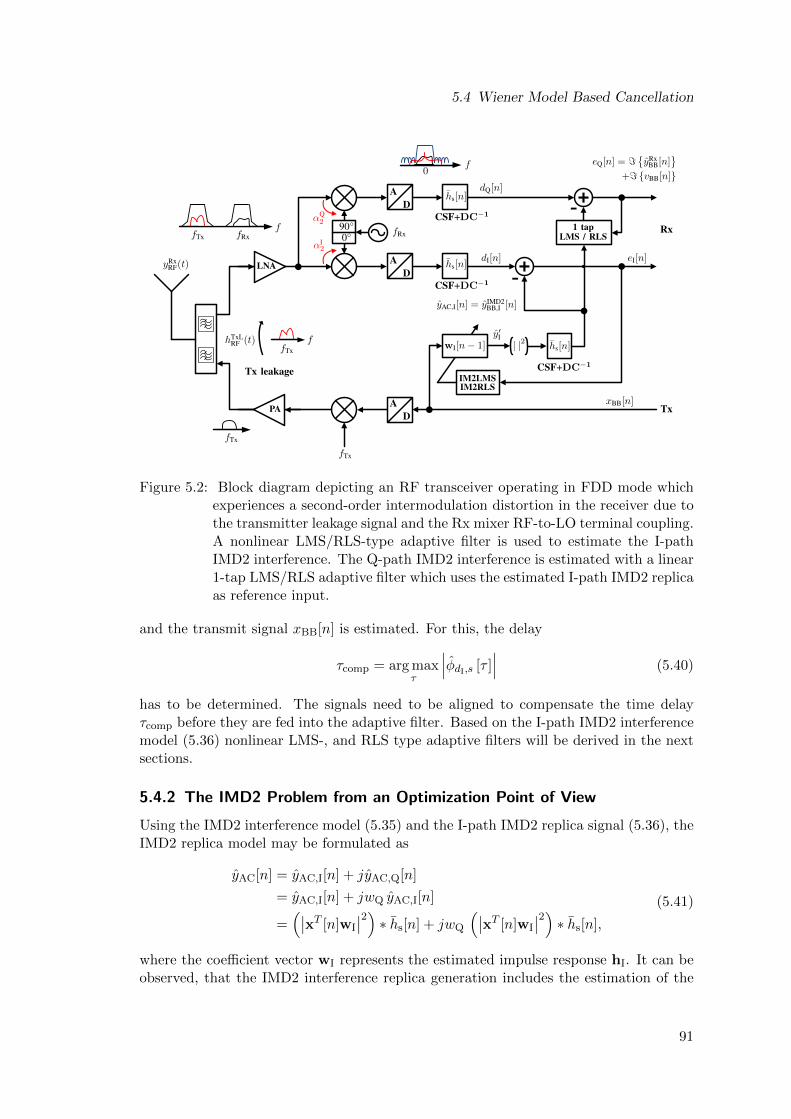
5.4 Wiener Model Based Cancellation
-
-
xBB[n]
yRxRF(t)
dQ[n]
dI[n]
wI[n− 1]y′I
yAC,I[n] = yIMD2BB,I [n]
eQ[n] = =yRx
BB[n]
+=vBB[n]
eI[n]
1 tapLMS / RLS
| |2
LNA
PA
hs[n]
hs[n]
hs[n]
CSF+DC−1
CSF+DC−1
CSF+DC−1
hTxLRF (t)
AD
AD
AD
IM2LMSIM2RLS
Tx leakage
fTx
fTx
fTx
fTx
fRxfRx
900
αQ2
αI2
f
f
0f
Rx
Tx
Figure 5.2: Block diagram depicting an RF transceiver operating in FDD mode whichexperiences a second-order intermodulation distortion in the receiver due tothe transmitter leakage signal and the Rx mixer RF-to-LO terminal coupling.A nonlinear LMS/RLS-type adaptive filter is used to estimate the I-pathIMD2 interference. The Q-path IMD2 interference is estimated with a linear1-tap LMS/RLS adaptive filter which uses the estimated I-path IMD2 replicaas reference input.
and the transmit signal xBB[n] is estimated. For this, the delay
τcomp = arg maxτ
∣∣∣φdI,s [τ ]∣∣∣ (5.40)
has to be determined. The signals need to be aligned to compensate the time delayτcomp before they are fed into the adaptive filter. Based on the I-path IMD2 interferencemodel (5.36) nonlinear LMS-, and RLS type adaptive filters will be derived in the nextsections.
5.4.2 The IMD2 Problem from an Optimization Point of View
Using the IMD2 interference model (5.35) and the I-path IMD2 replica signal (5.36), theIMD2 replica model may be formulated as
yAC[n] = yAC,I[n] + jyAC,Q[n]
= yAC,I[n] + jwQ yAC,I[n]
=(∣∣xT [n]wI
∣∣2)∗ hs[n] + jwQ
(∣∣xT [n]wI
∣∣2)∗ hs[n],
(5.41)
where the coefficient vector wI represents the estimated impulse response hI. It can beobserved, that the IMD2 interference replica generation includes the estimation of the
91
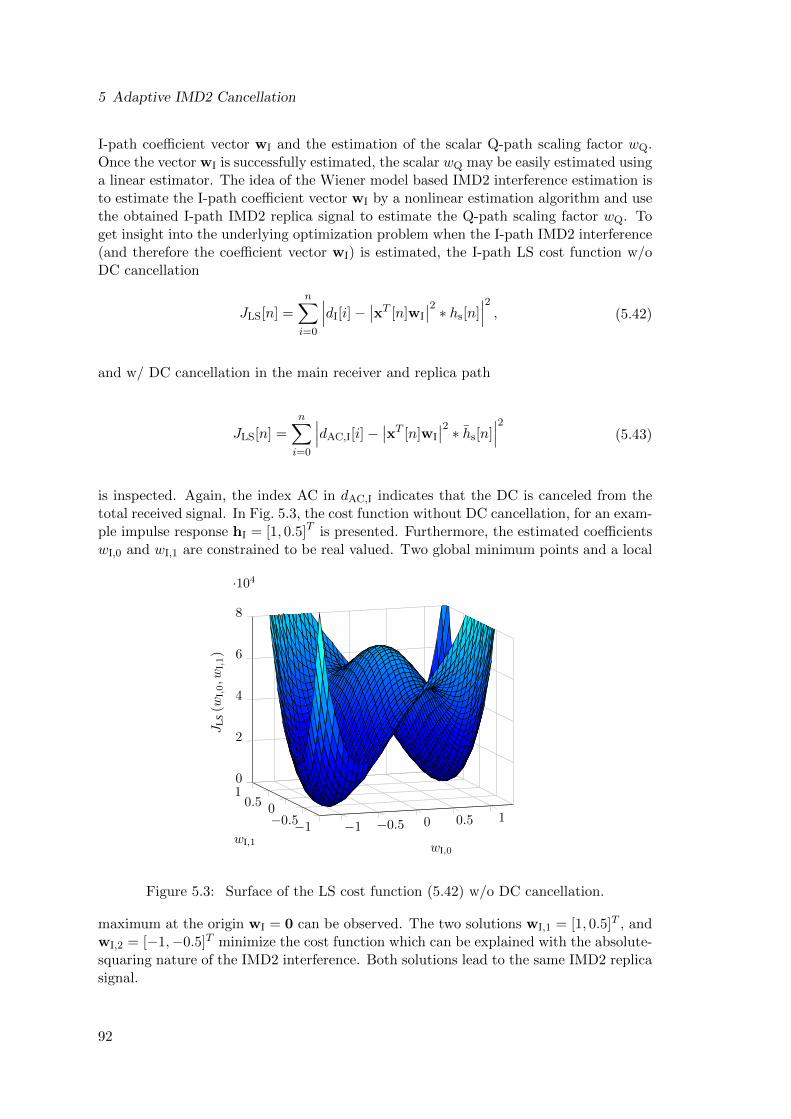
5 Adaptive IMD2 Cancellation
I-path coefficient vector wI and the estimation of the scalar Q-path scaling factor wQ.Once the vector wI is successfully estimated, the scalar wQ may be easily estimated usinga linear estimator. The idea of the Wiener model based IMD2 interference estimation isto estimate the I-path coefficient vector wI by a nonlinear estimation algorithm and usethe obtained I-path IMD2 replica signal to estimate the Q-path scaling factor wQ. Toget insight into the underlying optimization problem when the I-path IMD2 interference(and therefore the coefficient vector wI) is estimated, the I-path LS cost function w/oDC cancellation
JLS[n] =
n∑
i=0
∣∣∣dI[i]−∣∣xT [n]wI
∣∣2 ∗ hs[n]∣∣∣2, (5.42)
and w/ DC cancellation in the main receiver and replica path
JLS[n] =n∑
i=0
∣∣∣dAC,I[i]−∣∣xT [n]wI
∣∣2 ∗ hs[n]∣∣∣2
(5.43)
is inspected. Again, the index AC in dAC,I indicates that the DC is canceled from thetotal received signal. In Fig. 5.3, the cost function without DC cancellation, for an exam-ple impulse response hI = [1, 0.5]T is presented. Furthermore, the estimated coefficientswI,0 and wI,1 are constrained to be real valued. Two global minimum points and a local
−1 −0.5 0 0.5 1−1−0.500.5
10
2
4
6
8
·104
wI,0wI,1
JL
S(w
I,0,w
I,1)
Figure 5.3: Surface of the LS cost function (5.42) w/o DC cancellation.
maximum at the origin wI = 0 can be observed. The two solutions wI,1 = [1, 0.5]T , andwI,2 = [−1,−0.5]T minimize the cost function which can be explained with the absolute-squaring nature of the IMD2 interference. Both solutions lead to the same IMD2 replicasignal.
92
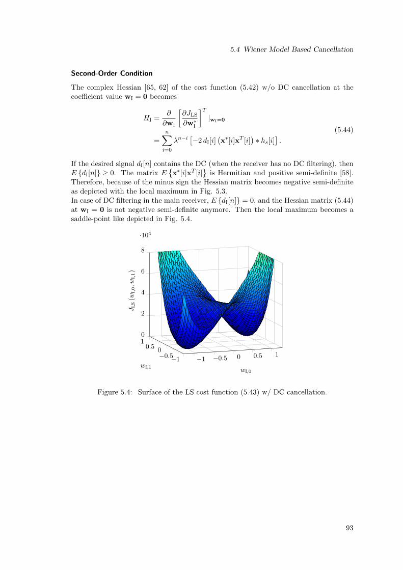
5.4 Wiener Model Based Cancellation
Second-Order Condition
The complex Hessian [65, 62] of the cost function (5.42) w/o DC cancellation at thecoefficient value wI = 0 becomes
HI =∂
∂wI
[∂JLS
∂w∗I
]T|wI=0
=n∑
i=0
λn−i[−2 dI[i]
(x∗[i]xT [i]
)∗ hs[i]
].
(5.44)
If the desired signal dI[n] contains the DC (when the receiver has no DC filtering), thenE dI[n] ≥ 0. The matrix E
x∗[i]xT [i]
is Hermitian and positive semi-definite [58].
Therefore, because of the minus sign the Hessian matrix becomes negative semi-definiteas depicted with the local maximum in Fig. 5.3.In case of DC filtering in the main receiver, E dI[n] = 0, and the Hessian matrix (5.44)at wI = 0 is not negative semi-definite anymore. Then the local maximum becomes asaddle-point like depicted in Fig. 5.4.
−1 −0.5 0 0.5 1−1−0.500.5
10
2
4
6
8
·104
wI,0wI,1
JL
S(w
I,0,w
I,1)
Figure 5.4: Surface of the LS cost function (5.43) w/ DC cancellation.
93
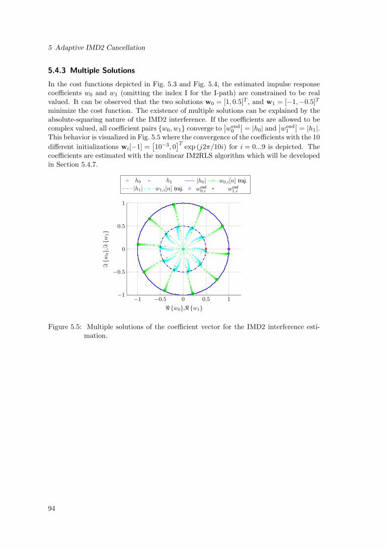
5 Adaptive IMD2 Cancellation
5.4.3 Multiple Solutions
In the cost functions depicted in Fig. 5.3 and Fig. 5.4, the estimated impulse responsecoefficients w0 and w1 (omitting the index I for the I-path) are constrained to be realvalued. It can be observed that the two solutions w0 = [1, 0.5]T , and w1 = [−1,−0.5]T
minimize the cost function. The existence of multiple solutions can be explained by theabsolute-squaring nature of the IMD2 interference. If the coefficients are allowed to becomplex valued, all coefficient pairs w0, w1 converge to
∣∣wend0
∣∣ = |h0| and∣∣wend
1
∣∣ = |h1|.This behavior is visualized in Fig. 5.5 where the convergence of the coefficients with the 10
different initializations wi[−1] =[10−3, 0
]Texp (j2π/10i) for i = 0...9 is depicted. The
coefficients are estimated with the nonlinear IM2RLS algorithm which will be developedin Section 5.4.7.
−1 −0.5 0 0.5 1−1
−0.5
0
0.5
1
<w0,<w1
=w
0,=w
1
h0 h1 |h0| w0,i[n] traj.|h1| w1,i[n] traj. wend
0,i wend1,i
Figure 5.5: Multiple solutions of the coefficient vector for the IMD2 interference esti-mation.
94
5.4 Wiener Model Based Cancellation
5.4.4 Wiener-Model LMS Based IMD2 Cancellation (IM2LMS)
In this section, a nonlinear Wiener model based LMS type adaptive algorithm (IM2LMS)to cancel the IMD2 interference is presented. In LMS based adaptive filters, the currentfilter output value is obtained by using the coefficient vector estimate of the previousiteration. This a-priori estimate wI[n − 1] is incorporated into the interference replicamodel (5.36) to develop a nonlinear LMS type adaptive filter to cancel the I-path IMD2interference in the digital baseband. Using an implicit DC cancellation, the DC value
E∣∣xT [n]wI
∣∣2
= wTI E
x[n]xH [n]
w∗I which is generated by the envelope-squaring
is implicitly subtracted within the adaptive filter. With this implicit DC cancellationapproach, the DC-filtering at the output of the interference replica model (5.36) may bereplaced. This leads to the I-path IMD2 replica generation
yAC,I[n] =(∣∣xT [n]wI[n− 1]
∣∣2)∗ hs[n]
=([∣∣xT [n]wI[n− 1]
∣∣2 −wTI [n− 1]E
x[n]xH [n]
w∗I [n− 1]
])∗ hs[n]
=([∣∣xT [n]wI[n− 1]
∣∣2 −wTI [n− 1]Rxxw∗I [n− 1]
])∗ hs[n]
=([
wTI [n− 1]
(x[n]xH [n]−Rxx
)w∗I [n− 1]
])∗ hs[n]
(5.45)
where the autocorrelation matrix Rxx = Ex[n]xH [n]
is used2. Assuming real valued
CSF impulse response coefficients hs[n], and observing that dAC,I[i] is the desired signalin the I-path, and therefore real valued, the instantaneous squared error cost functionbased on the error
eAC,I[n] = dAC,I[n]− yAC,I[n] (5.46)
becomes
J = |eAC,I[n]|2
=∣∣dAC,I[n]−
[wT
I [n− 1](x[n]xH [n]−Rxx
)w∗I [n− 1]
]∗ hs[n]
∣∣2
= d2AC,I[n]− 2 dAC,I[n]
[wT
I [n− 1](x[n]xH [n]−Rxx
)w∗I [n− 1]
]∗ hs[n]
+([
wTI [n− 1]
(x[n]xH [n]−Rxx
)w∗I [n− 1]
]∗ hs[n]
)2.
(5.47)
To develop a stochastic-gradient LMS type estimation algorithm, the R∗-derivative (seeSection 4.3) of the cost function (5.47) is evaluated which becomes
[∂J
∂w∗I
]T=[−2 dAC,I[n]
[wT
I [n− 1](x[n]xH [n]−Rxx
)]∗ hs[n]
+ 2([
wTI [n− 1]
(x[n]xH [n]−Rxx
)w∗I [n− 1]
]∗ hs[n]
)
·[wT
I [n− 1](x[n]xH [n]−Rxx
)]∗ hs[n]
]T.
(5.48)
A detailed derivation of the derivative (5.48) incorporating the channel-select filter in thecost function (5.47) is presented in Appendix A.5. By using the IMD2 replica yAC,I[n]
2An autocorrelation matrix Rxx is defined for wide-sense stationary signals. Each LTE symbol can beconsidered as a section of a wide-sense stationary signal. However, subsequent symbols are statisti-cally independent. But it makes sense to introduce an Rxx because the length of w is much smallerthan the symbol duration.
95
5 Adaptive IMD2 Cancellation
and the a priori FIR filter output y′[n] = xT [n]wI[n− 1], the derivative is simplified to
[∂J
∂w∗I
]T= − (2 dAC,I[n]− 2 yAC,I[n])
[[wT
I [n− 1](x[n]xH [n]−Rxx
)]∗ hs[n]
]T
= −2 eAC,I[n][(y′[n]x∗[n]−RT
xxwI[n− 1])∗ hs[n]
] (5.49)
which leads to the stochastic gradient coefficient update
wI[n] = wI[n− 1]− 2µ
[∂J
∂w∗I
]T
= wI[n− 1] + 4µeAC,I[n][(y′[n]x∗[n]−RT
xxwI[n− 1])∗ hs[n]
] (5.50)
with the step-size µ.
Normalization of the IM2LMS algorithm
In the IMD2 LMS type adaptive filter, the a priori error signal
eAC,I[n] = dAC,I[n]−[∣∣xT [n]wI[n− 1]
∣∣2 −wTI [n− 1]Rxxw∗I [n− 1]
]∗ hs[n] (5.51)
is used to update the filter coefficients. To analyze the convergence of the LMS typealgorithm (5.50) it is beneficial to analyze the relationship between the errors eAC,I[n] andeAC,I[n+1] [58, 66]. For this, a first order Taylor series expansion of the non-holomorphicterm eAC,I[n] with respect to the coefficient vector is needed. As a reminder, in thederivation of the ε-NLMS (Algorithm 1), the term e[n] was holomorphic and thereforethe standard complex derivative was applied to derive the Taylor series expansion. Forthe nonlinear IM2LMS case, eAC,I[n] is real valued and a function of the complex vectorwI[n − 1]. In this case the first-order Taylor expansion becomes (see equation (85) in[67])
eAC,I[n+ 1] ≈ eAC,I[n] + 2<∂eAC,I[n]
∂wI[n− 1]∆wI[n]
(5.52)
and by using the IMD2-nonlinearity φ(·) = |·|2 and y′[n] = xT [n]wI[n− 1] it follows that
∂eAC,I[n]
∂wI[n− 1]= −
(∂φ (y′)
∂y′∂y′
∂wI[n− 1]−wH
I [n− 1]RTxx
)∗ hs
= −(y′∗[n]xT [n]−wH
I [n− 1]RTxx
)∗ hs.
(5.53)
With∆wI[n] = 4µeAC,I[n]
[(y′[n]x∗[n]−RT
xxwI[n− 1])∗ hs[n]
], (5.54)
the first-order Taylor series expansion (5.52) becomes
eAC,I[n+ 1] ≈ eAC,I[n]− 2<[(
y′∗[n]xT [n]−wHI [n− 1]RT
xx
)∗ hs
]
·4µeAC,I[n][(y′[n]x∗[n]−RT
xxwI[n− 1])∗ hs[n]
]
≈(
1− 8µ[(∣∣y′[n]
∣∣2 xH [n]x[n]− 2<y′∗[n]xT [n]RT
xxwI[n− 1]
+wHI [n− 1]
(RT
xx
)2wI[n− 1]
)∗ hs[n]
])eAC,I[n]
≈ (1− 8µΨ[n]) eAC,I[n],
(5.55)
96
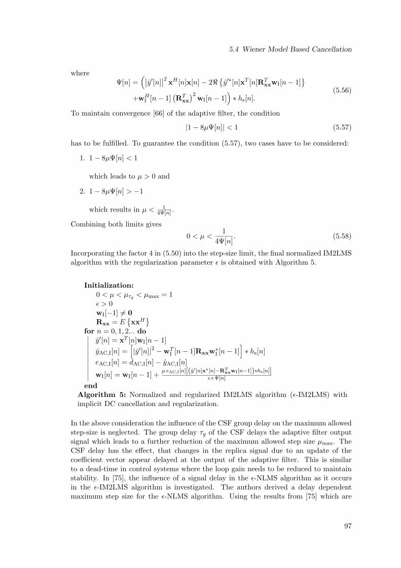
5.4 Wiener Model Based Cancellation
whereΨ[n] =
(∣∣y′[n]∣∣2 xH [n]x[n]− 2<
y′∗[n]xT [n]RT
xxwI[n− 1]
+wHI [n− 1]
(RT
xx
)2wI[n− 1]
)∗ hs[n].
(5.56)
To maintain convergence [66] of the adaptive filter, the condition
|1− 8µΨ[n]| < 1 (5.57)
has to be fulfilled. To guarantee the condition (5.57), two cases have to be considered:
1. 1− 8µΨ[n] < 1
which leads to µ > 0 and
2. 1− 8µΨ[n] > −1
which results in µ < 14Ψ[n] .
Combining both limits gives
0 < µ <1
4Ψ[n]. (5.58)
Incorporating the factor 4 in (5.50) into the step-size limit, the final normalized IM2LMSalgorithm with the regularization parameter ε is obtained with Algorithm 5.
Initialization:0 < µ < µτg < µmax = 1ε > 0wI[−1] 6= 0Rxx = E
xxH
for n = 0, 1, 2... doy′[n] = xT [n]wI[n− 1]
yAC,I[n] =[|y′[n]|2 −wT
I [n− 1]Rxxw∗I [n− 1]]∗ hs[n]
eAC,I[n] = dAC,I[n]− yAC,I[n]
wI[n] = wI[n− 1] +µ eAC,I[n][(y′[n]x∗[n]−RT
xxwI[n−1])∗hs[n]]ε+Ψ[n]
endAlgorithm 5: Normalized and regularized IM2LMS algorithm (ε-IM2LMS) withimplicit DC cancellation and regularization.
In the above consideration the influence of the CSF group delay on the maximum allowedstep-size is neglected. The group delay τg of the CSF delays the adaptive filter outputsignal which leads to a further reduction of the maximum allowed step size µmax. TheCSF delay has the effect, that changes in the replica signal due to an update of thecoefficient vector appear delayed at the output of the adaptive filter. This is similarto a dead-time in control systems where the loop gain needs to be reduced to maintainstability. In [75], the influence of a signal delay in the ε-NLMS algorithm as it occursin the ε-IM2LMS algorithm is investigated. The authors derived a delay dependentmaximum step size for the ε-NLMS algorithm. Using the results from [75] which are
97
5 Adaptive IMD2 Cancellation
also applicable for the ε-IM2LMS algorithm, the final CSF delay dependent maximumstep-size becomes
µτg = µmaxsin
(π
2 (2τg + 1)
), (5.59)
where the delay τg in samples is used. Simulations confirmed that by choosing the max-imum step-size according to (5.59), Algorithm 5 remains stable for arbitrary delays τg.
The usual choice of the zero-vector as initialization of wI[−1] results in a vanishingderivative (5.49) for all n. This is due to the nature of the cost function (5.42) depictedin Fig. 5.3 having a local maximum at wI = 0 and therefore a vanishing derivative. Ifthe DC is canceled, the cost function (5.43) has a saddle point at wI = 0 which causes avanishing derivative, too. Consequently, the Wiener model based algorithm needs to beinitialized with wI[−1] 6= 0. If no prior knowledge about the Tx-to-Rx leakage channel isavailable, an initialization close to the zero vector, e.g., wI[−1] = [wI,0, 0, 0, ..., 0]T wherewI,0 is a small real valued positive number is a reasonable choice.
The derived nonlinear Wiener model based LMS type algorithm uses the autocorre-lation matrix to perform an implicit DC cancellation. The implied vector-matrix multi-plication increases the computational complexity of the LMS type algorithm and lowerstherefore its applicability in real applications. Furthermore, each entry of the coefficientupdate vector needs to be channel-select filtered which results in further computationalload. To overcome these two limitations, reduced complexity variants of Algorithm 5are developed in the next section.
5.4.5 Reduced Complexity IM2LMS Algorithm
The complexity of the digital IMD2 cancellation is significantly reduced by using theWiener model instead of the Volterra model. However, the channel-select filtering of thecoefficient update vector in the IM2LMS algorithm and the DC cancellation contribute toa much higher complexity compared to the traditional linear LMS. Furthermore, for in-terference cancellation in RF transceivers the adaptive filter input signal is an SC-FDMAmodulated transmit signal. These signals are not wide-sense stationary since subsequentsymbols are statistically independent, and therefore the autocorrelation matrix Rxx isnot defined. It still makes sense to introduce an Rxx because the length of w is muchsmaller than the symbol duration, and each LTE symbol can be considered as a sectionof a wide-sense stationary signal. However, it turned out that the usage of σ2
xI insteadof Rxx leads to good cancellation results, which can be used to reduce the complexityof the algorithm. The next sections will address possible complexity reductions for theIM2LMS algorithm.
Reducing the Complexity of the Implicit DC Cancellation
The implicit DC cancellation using the expression wTI [n− 1]Rxxw∗I [n− 1] increases the
complexity to the order O(M2). In order to simplify the implicit DC cancellation theexpression σ2
xI is used instead of Rxx. By using this approximation, the DC value in
98
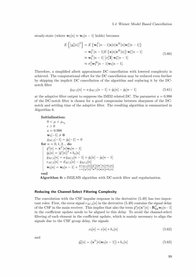
5.4 Wiener Model Based Cancellation
steady-state (where wI[n] ≈ wI[n− 1] holds) becomes
E∣∣y′I[n]
∣∣2
= EwT
I [n− 1]x[n]xH [n]w∗I [n− 1]
= wTI [n− 1]E
x[n]xH [n]
w∗I [n− 1]
≈ wTI [n− 1]
[σ2xI]w∗I [n− 1]
≈ σ2xw
HI [n− 1]wI[n− 1].
(5.60)
Therefore, a simplified albeit approximate DC cancellation with lowered complexity isachieved. The computational effort for the DC cancellation may be reduced even furtherby skipping the implicit DC cancellation of the algorithm and replacing it by the DC-notch filter
yAC,I[n] = a yAC,I[n− 1] + yI[n]− yI[n− 1] (5.61)
at the adaptive filter output to suppress the IMD2 related DC. The parameter a = 0.998of the DC-notch filter is chosen for a good compromise between sharpness of the DC-notch and settling time of the adaptive filter. The resulting algorithm is summarized inAlgorithm 6.
Initialization:0 < µ < µτgε > 0a = 0.998wI[−1] 6= 0yAC,I[−1] = yI[−1] = 0
for n = 0, 1, 2... doy′[n] = xT [n]wI[n− 1]yI[n] = |y′[n]|2 ∗ hs[n]yAC,I[n] = a yAC,I[n− 1] + yI[n]− yI[n− 1]eAC,I[n] = dAC,I[n]− yAC,I[n]
wI[n] = wI[n− 1] +µ eAC,I[n][(y′[n]x∗[n])∗hs[n]]
ε+(|y′[n]|2xH [n]x[n])∗hs[n]
endAlgorithm 6: ε-IM2LMS algorithm with DC-notch filter and regularization.
Reducing the Channel-Select Filtering Complexity
The convolution with the CSF impulse response in the derivative (5.49) has two impor-tant roles: First, the error signal eAC,I[n] in the derivative (5.49) contains the signal delayof the CSF in the main receiver. This implies that also the term y′[n]x∗[n]−RT
xxwI[n−1]in the coefficient update needs to be aligned to this delay. To avoid the channel-selectfiltering of each element in the coefficient update, which is mainly necessary to align thesignals due to the CSF group delay, the signals
xf[n] = x[n] ∗ hs[n] (5.62)
and
y′f[n] =(xT [n]wI[n− 1]
)∗ hs[n] (5.63)
99
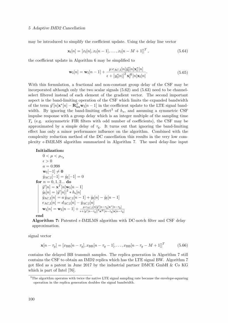
5 Adaptive IMD2 Cancellation
may be introduced to simplify the coefficient update. Using the delay line vector
xf[n] = [xf[n], xf[n− 1], . . . , xf[n−M + 1]]T , (5.64)
the coefficient update in Algorithm 6 may be simplified to
wI[n] = wI[n− 1] +µ eAC,I[n]y′f[n]x∗f [n]
ε+∣∣y′f[n]
∣∣2 xHf [n]xf[n]. (5.65)
With this formulation, a fractional and non-constant group delay of the CSF may beincorporated although only the two scalar signals (5.62) and (5.63) need to be channel-select filtered instead of each element of the gradient vector. The second importantaspect is the band-limiting operation of the CSF which limits the expanded bandwidthof the term y′[n]x∗[n]−RT
xxwI[n− 1] in the coefficient update to the LTE signal band-width. By ignoring the band-limiting effect3 of hs, and assuming a symmetric CSFimpulse response with a group delay which is an integer multiple of the sampling timeTs (e.g. axisymmetric FIR filters with odd number of coefficients), the CSF may beapproximated by a simple delay of τg. It turns out that ignoring the band-limitingeffect has only a minor performance influence on the algorithm. Combined with thecomplexity reduction method of the DC cancellation this results in the very low com-plexity ε-IM2LMS algorithm summarized in Algorithm 7. The used delay-line input
Initialization:0 < µ < µτgε > 0a = 0.998wI[−1] 6= 0yAC,I[−1] = yI[−1] = 0
for n = 0, 1, 2... doy′[n] = xT [n]wI[n− 1]yI[n] = |y′[n]|2 ∗ hs[n]yAC,I[n] = a yAC,I[n− 1] + yI[n]− yI[n− 1]eAC,I[n] = dAC,I[n]− yAC,I[n]
wI[n] = wI[n− 1] +µ eAC,I[n]y′[n−τg]x∗[n−τg]
ε+|y′[n−τg]|2xH [n−τg]x[n−τg]
endAlgorithm 7: Patented ε-IM2LMS algorithm with DC-notch filter and CSF delayapproximation.
signal vector
x[n− τg] = [xBB[n− τg], xBB[n− τg − 1], . . . , xBB[n− τg −M + 1]]T (5.66)
contains the delayed BB transmit samples. The replica generation in Algorithm 7 stillcontains the CSF to obtain an IMD2 replica which has the LTE signal BW. Algorithm 7got filed as a patent in June 2017 by the industrial partner DMCE GmbH & Co KGwhich is part of Intel [76].
3The algorithm operates with twice the native LTE signal sampling rate because the envelope-squaringoperation in the replica generation doubles the signal bandwidth.
100
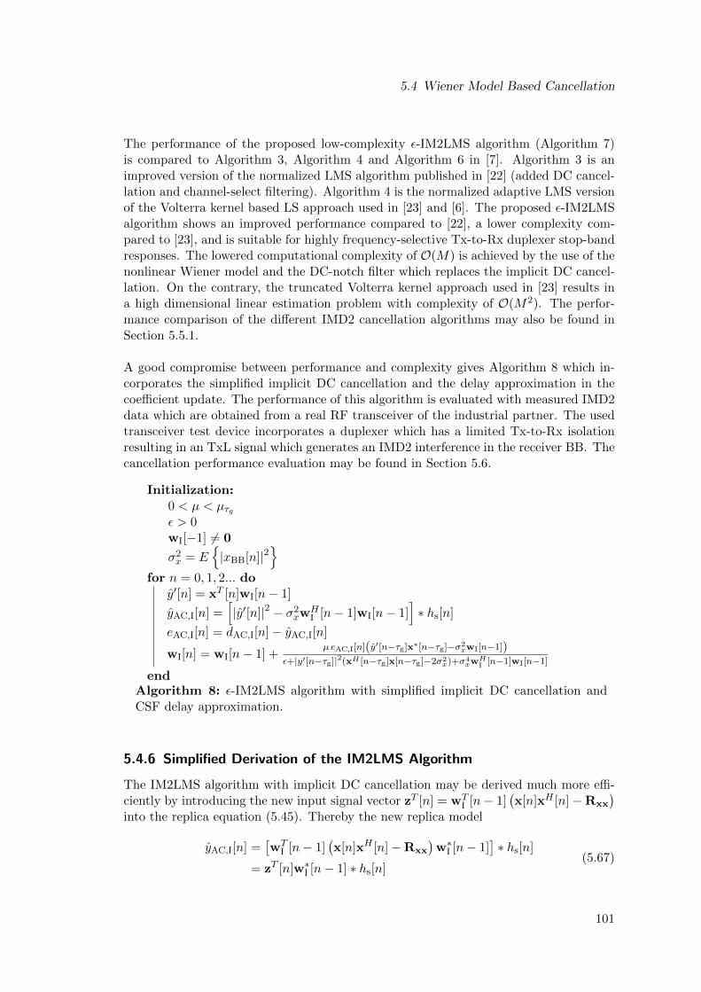
5.4 Wiener Model Based Cancellation
The performance of the proposed low-complexity ε-IM2LMS algorithm (Algorithm 7)is compared to Algorithm 3, Algorithm 4 and Algorithm 6 in [7]. Algorithm 3 is animproved version of the normalized LMS algorithm published in [22] (added DC cancel-lation and channel-select filtering). Algorithm 4 is the normalized adaptive LMS versionof the Volterra kernel based LS approach used in [23] and [6]. The proposed ε-IM2LMSalgorithm shows an improved performance compared to [22], a lower complexity com-pared to [23], and is suitable for highly frequency-selective Tx-to-Rx duplexer stop-bandresponses. The lowered computational complexity of O(M) is achieved by the use of thenonlinear Wiener model and the DC-notch filter which replaces the implicit DC cancel-lation. On the contrary, the truncated Volterra kernel approach used in [23] results ina high dimensional linear estimation problem with complexity of O(M2). The perfor-mance comparison of the different IMD2 cancellation algorithms may also be found inSection 5.5.1.
A good compromise between performance and complexity gives Algorithm 8 which in-corporates the simplified implicit DC cancellation and the delay approximation in thecoefficient update. The performance of this algorithm is evaluated with measured IMD2data which are obtained from a real RF transceiver of the industrial partner. The usedtransceiver test device incorporates a duplexer which has a limited Tx-to-Rx isolationresulting in an TxL signal which generates an IMD2 interference in the receiver BB. Thecancellation performance evaluation may be found in Section 5.6.
Initialization:0 < µ < µτgε > 0wI[−1] 6= 0
σ2x = E
|xBB[n]|2
for n = 0, 1, 2... doy′[n] = xT [n]wI[n− 1]
yAC,I[n] =[|y′[n]|2 − σ2
xwHI [n− 1]wI[n− 1]
]∗ hs[n]
eAC,I[n] = dAC,I[n]− yAC,I[n]
wI[n] = wI[n− 1] +µ eAC,I[n](y′[n−τg]x∗[n−τg]−σ2
xwI[n−1])ε+|y′[n−τg]|2(xH [n−τg]x[n−τg]−2σ2
x)+σ4xwH
I [n−1]wI[n−1]
endAlgorithm 8: ε-IM2LMS algorithm with simplified implicit DC cancellation andCSF delay approximation.
5.4.6 Simplified Derivation of the IM2LMS Algorithm
The IM2LMS algorithm with implicit DC cancellation may be derived much more effi-ciently by introducing the new input signal vector zT [n] = wT
I [n− 1](x[n]xH [n]−Rxx
)
into the replica equation (5.45). Thereby the new replica model
yAC,I[n] =[wT
I [n− 1](x[n]xH [n]−Rxx
)w∗I [n− 1]
]∗ hs[n]
= zT [n]w∗I [n− 1] ∗ hs[n](5.67)
101
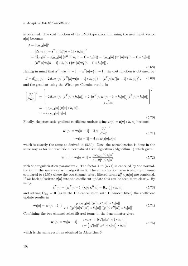
5 Adaptive IMD2 Cancellation
is obtained. The cost function of the LMS type algorithm using the new input vectorz[n] becomes
J = |eAC,I[n]|2
=∣∣dAC,I[n]− zT [n]w∗I [n− 1] ∗ hs[n]
∣∣2
= d2AC,I[n]− dAC,I[n]
(zH [n]wI[n− 1] ∗ hs[n]
)− dAC,I[n]
(zT [n]w∗I [n− 1] ∗ hs[n]
)
+(zH [n]wI[n− 1] ∗ hs[n]
) (zT [n]w∗I [n− 1] ∗ hs[n]
).
(5.68)Having in mind that zH [n]wI[n− 1] = zT [n]w∗I [n− 1], the cost function is obtained by
J = d2AC,I[n]− 2 dAC,I[n]
(zH [n]wI[n− 1] ∗ hs[n]
)+(zT [n]w∗I [n− 1] ∗ hs[n]
)2, (5.69)
and the gradient using the Wirtinger Calculus results in
[∂J
∂w∗I
]T=
−2 dAC,I[n]
(zT [n] ∗ hs[n]
)+ 2
(zH [n]wI[n− 1] ∗ hs[n]
)︸ ︷︷ ︸
yAC,I[n]
(zT [n] ∗ hs[n]
)
T
= −2 eAC,I[n] (z[n] ∗ hs[n])
= −2 eAC,I[n]zf[n].(5.70)
Finally, the stochastic gradient coefficient update using zf[n] = z[n] ∗ hs[n] becomes
wI[n] = wI[n− 1]− 2µ
[∂J
∂w∗I
]T
= wI[n− 1] + 4µeAC,I[n]zf[n]
(5.71)
which is exactly the same as derived in (5.50). Now, the normalization is done in thesame way as for the traditional normalized LMS algorithm (Algorithm 1) which gives
wI[n] = wI[n− 1] +µ eAC,I[n]zf[n]
ε+ zHf [n]zf[n](5.72)
with the regularization parameter ε. The factor 4 in (5.71) is canceled by the normal-ization in the same way as in Algorithm 5. The normalization term is slightly differentcompared to (5.55) where the two channel-select filtered terms zHf [n]zf[n] are combined.If we back substitute z[n] into the coefficient update this can be seen more clearly. Byusing
zTf [n] =[wT
I [n− 1](x[n]xH [n]−Rxx
)]∗ hs[n] (5.73)
and setting Rxx = 0 (as in the DC cancellation with DC-notch filter) the coefficientupdate results in
wI[n] = wI[n− 1] +µ eAC,I[n] [(y′[n]x∗[n]) ∗ hs[n]]
ε+ [(y′∗[n]xT [n]) ∗ hs[n]] [(y′[n]xH [n]) ∗ hs[n]]. (5.74)
Combining the two channel-select filtered terms in the denominator gives
wI[n] = wI[n− 1] +µ eAC,I[n] [(y′[n]x∗[n]) ∗ hs[n]]
ε+(|y′[n]|2 xH [n]x[n]
)∗ hs[n]
(5.75)
which is the same result as obtained in Algorithm 6.
102
5.4 Wiener Model Based Cancellation
5.4.7 Wiener-Model RLS Based IMD2 Cancellation (IM2RLS)
In this section, a nonlinear Wiener model based RLS type adaptive algorithm (IM2RLS)with exponential forgetting factor is derived. It is suitable for highly frequency selectiveduplexer stop-band frequency responses like indicated in Fig. 2.12 and targets the digitalIMD2 cancellation for high performance cellular base stations and mobile phones. Thederived IM2RLS algorithm is further extended by a regularization (R-IM2RLS) whichmakes the algorithm applicable for highly correlated BB transmit signals where theautocorrelation matrix can be close to singular. A high correlation in the transmit signalcan be due to oversampling which happens e.g. in the case of multi-cluster transmissions(introduced in 3GPP LTE-A Release 11) where only a part of the available resourceblocks (RBs) are allocated. The presented IM2RLS algorithm is an extension to the ε-IM2LMS algorithm which is derived in section 5.4.4 and published in [7]. The IM2RLSalgorithm offers an improved steady-state cancellation and faster adaptation. Using thereplica model (5.36) with implicit DC cancellation
yAC,I[n] =∣∣xT [n]wI[n]
∣∣2 ∗ hs[n]
=[wT
I [n](x[n]xH [n]−Rxx
)w∗I [n]
]∗ hs[n],
(5.76)
the LS cost function up to the time index n with the exponential forgetting factor0 λ ≤ 1 becomes
JLS[n] =
n∑
i=0
λn−i∣∣dAC,I[i]−
[wT
I [n](x[i]xH [i]−Rxx
)w∗I [n]
]∗ hs[i]
∣∣2 . (5.77)
Assuming real valued CSF impulse response coefficients hs[n], and observing that dAC,I[i]is the desired signal in the I-path, and therefore real valued, the Wirtinger derivative ofthe cost function (5.77) may be derived. The R∗ Wirtinger derivative (see Section 4.3)becomes
[∂JLS[n]
∂w∗I [n]
]T=
n∑
i=0
λn−i−2 dAC,I[i]
[(x∗[i]xT [i]−RT
xx
)wI[n] ∗ hs[i]
]
+2[(
x∗[i]xT [i]−RTxx
)wI[n] ∗ hs[i]
]
·[wH [n]
(x∗[i]xT [i]−R∗xx
)∗ hs[i]
]wI[n]
.
(5.78)
The detailed derivation of the derivative (5.78) can be found in Appendix A.5. By settingthe derivative to zero, an equation similar to the Wiener-Hopf equation is obtained:
R (wI[n]) wI[n] = r (wI[n]) (5.79)
However, it can be observed that the matrix
R =
n∑
i=0
λn−i[(
x∗[i]xT [i]−RTxx
)wI[n] ∗ hs[i]
]
·[wH [n]
(x∗[i]xT [i]−R∗xx
)∗ hs[i]
]wI[n]
(5.80)
and the vector
r =
n∑
i=0
λn−idAC,I[i]
[(x∗[i]xT [i]−RT
xx
)wI[n] ∗ hs[i]
](5.81)
103
5 Adaptive IMD2 Cancellation
are functions of the unknown coefficient vector wI[n]. In a slowly varying or nearlystationary system environment it may be assumed that xT [i]w[n] ≈ xT [i]w[i− 1] whenthe index i is close to n [77, 78]. If the index i << n, the approximation introducesan error which is however attenuated by the forgetting factor. Defining the new costfunction
J ′LS[n] =n∑
i=0
λn−i∣∣dAC,I[i]−
[wT
I [i− 1](x[i]xH [i]−Rxx
)w∗I [n]
]∗ hs[i]
∣∣2 (5.82)
where wTI [i − 1] is used instead of wT
I [n] we can overcome this limitation. As a nextstep, the same input vector zT [i] = wT
I [i− 1](x[i]xH [i]−Rxx
)as it was used in the
simplified derivation of the ε-IM2LMS algorithm is introduced, such that the new costfunction becomes
J ′LS[n] =n∑
i=0
λn−i∣∣dAC,I[i]− zT [i]w∗I [n] ∗ hs[i]
∣∣2
=
n∑
i=0
λn−i |eAC,I[i]|2 .(5.83)
Following the traditional RLS derivation provided in Section 4.5, the IM2RLS algorithmto estimate the I-path IMD2 interference in the digital BB is summarized in Algorithm 9.Here, the channel-select filtered vector zTf [n] = zT [n] ∗ hs[n] is used to align the signalsaccording to the delay introduced by the CSF. Because the error signal eAC,I[n] is realvalued, its conjugation in the coefficient update equation is omitted. The usual choiceof the zero-vector as initialization of wI[−1] results in a zero-gain vector k[n] for alln. This is reasoned in the cost function (5.77) depicted in Fig. 5.4 which has a saddlepoint at wI = 0 and therefore a vanishing derivative. Consequently, the algorithm isinitialized with wI[−1] 6= 0, and with the parameters 0 λ ≤ 1, and P[−1] = ν I withν > 0. However, as for the ε-IM2LMS algorithm, an initialization close to the zero vector,e.g., wI[−1] = [wI,0, 0, 0, .., 0]T where wI,0 is a small real valued positive number can beused.
Reducing the Complexity of the Implicit DC Cancellation
In the ε-IM2LMS algorithm, the usage of σ2xI instead of Rxx leads to good cancellation
results. This simplification can also be used to reduce the complexity of the IM2RLSalgorithm. A further complexity reduction may be achieved by using the DC-notch filter(5.61) for the DC cancellation which has the advantage that the knowledge of the Txsignal statistics is not necessary. The parameter a determines the sharpness of the DC-notch. If the parameter a is chosen close to unity, the filter has a very sharp notch atDC but needs longer to settle which may influence the convergence time of the adaptivefilter.
Reducing the Channel-Select Filtering Complexity
To avoid the channel-select filtering of the M elements in the vector zf[n] = z[n] ∗ hs[n],which is mainly necessary to align the signals due to the CSF group delay, the signals
104
5.4 Wiener Model Based Cancellation
Initialization:P[−1] = ν I with ν > 00 λ ≤ 1wI[−1] 6= 0Rxx = E
xxH
for n = 0, 1, 2... dozT [n] = wT
I [n− 1](x[n]xH [n]−Rxx
)
zf[n] = z[n] ∗ hs[n]yAC,I[n] = zT [n]w∗I [n− 1] ∗ hs[n]eAC,I[n] = dAC,I[n]− yAC,I[n]
k[n] = P[n−1]zf[n]
λ+zHf [n]P[n−1]zf[n]
P[n] = 1λ
[P[n− 1]− k[n]zHf [n]P[n− 1]
]
wI[n] = wI[n− 1] + eAC,I[n]k[n]
endAlgorithm 9: IM2RLS algorithm with implicit DC cancellation using the autocor-relation matrix Rxx.
xf[n] = x[n] ∗ hs[n] and y′f[n] = xT [n]wI[n− 1] ∗ hs[n] may be introduced. Using the de-lay line vector
xf[n] = [xf[n], xf[n− 1], . . . , xf[n−M + 1]]T , (5.84)
the vector zf[n] may be approximated by
zf[n] ≈ y′f[n]x∗f [n]. (5.85)
By using this formulation in Algorithm 9 only two scalar signals need to be filteredwith the CSF impulse response. A big advantage of this simplification is, that also afractional and non-constant group delay of the CSF may be incorporated. However, inthis approximation the band-limiting effect of the CSF on zf[n] is ignored. This may betolerated due to the oversampling factor (OSF) of 2 which is anyhow necessary becauseof the envelope-squaring in the replica generation.
Channel-Select Filter Delay-Approximation
If the group delay τg of the CSF is constant and an integer multiple of the samplingtime (e.g. axisymmetric FIR filters with odd number of coefficients), the CSF may beapproximated by a simple signal delay given by
zf[n] ≈ z[n− τg]. (5.86)
Also in this approximation the band-limiting effect of the CSF on z[n] is ignored but maybe tolerated because of the OSF of 2. The resulting IM2RLS algorithm with DC-notchfilter and CSF delay-approximation is summarized in Algorithm 10. The performanceof Algorithm 10 is presented in [27] where it shows an excellent IMD2 self-interferencecancellation for a full allocated LTE10 transmit signal. However, to improve numericalstability for small bandwidth allocations like, e.g., used in multi-cluster transmissions,the regularized IM2RLS (R-IM2RLS) is derived in the next section.
105
5 Adaptive IMD2 Cancellation
Initialization:P[−1] = ν I with ν > 00 λ ≤ 1wI[−1] 6= 0a = 0.998yAC,I[−1] = yI[−1] = 0
for n = 0, 1, 2... dozT [n] = wT
I [n− 1]x[n]xH [n]zf[n] = z[n− τg]yI[n] = zT [n]w∗I [n− 1] ∗ hs[n]yAC,I[n] = a yAC,I[n− 1] + yI[n]− yI[n− 1]eAC,I[n] = dAC,I[n]− yAC,I[n]
k[n] = P[n−1]zf[n]
λ+zHf [n]P[n−1]zf[n]
P[n] = 1λ
[P[n− 1]− k[n]zHf [n]P[n− 1]
]
wI[n] = wI[n− 1] + eAC,I[n]k[n]
endAlgorithm 10: IM2RLS algorithm with DC cancellation using a DC-notch filterand CSF delay approximation.
Tikhonov Regularization of the nonlinear IM2RLS
To reduce the spectral OOB emission of the LTE signals, not all available subcarriersare allocated. A portion of the subcarriers at the band-edges (guard-band) are forcedto zero which introduces correlation in the transmit BB samples. E.g. in a 10 MHz LTEsignal a maximum of 600 out of 1024 subcarriers may be occupied by data [79]. Thiscorrelation in the Tx BB signal xBB[n] leads to a badly-conditioned autocorrelation ma-trix4 R = E
xBB[n]xHBB[n]
and respectively R = E
zf[n]zHf [n]
. Algorithms which
need the estimation of the autocorrelation matrix or its inverse P = R−1 are sensitiveto the condition number of R and may suffer from numerical instability if R is badly-conditioned. Therefore, a regularized version of the IM2RLS algorithm (R-IM2RLS) isderived in this section.
A common method to overcome the problem of badly-conditioned autocorrelation ma-trices is regularization [61]. Adding a positive definite matrix to the estimated auto-correlation matrix in each iteration of the RLS algorithm guarantees that the regularizedautocorrelation matrix R′ stays positive definite and therefore maintains the necessarycondition for convergence and existence of P = R′−1 [80].This method is commonly known as Tikhonov-regularization where a matrix L is usedfor the regularization [81]. By including a regularization term in the cost function (5.83),
4The LTE transmit signal is not wide-sense stationary. However, each LTE symbol can be consideredas a section of a wide-sense stationary signal. Therefore, because the length of w is much smallerthan the symbol duration it makes sense to introduce the matrix R = E
zf[n]zHf [n]
.
106
5.4 Wiener Model Based Cancellation
the new cost function
J ′R[n] =
n∑
i=0
λn−i[|eAC,I[i]|2 + σ ‖LwI[n]‖22
]
=n∑
i=0
λn−i[|eAC,I[i]|2 + σwT
I [n]LTLw∗I [n]] (5.87)
is defined where eAC,I[i] = dAC,I[i] −(zT [i]w∗I [n]
)∗ hs[i]. The regularization parameter
σ ≥ 0 is used to adjust the amount of regularization and the real valued matrix L istypically chosen as L = I (standard Tikhonov regularization),
L =
−1 1−1 1
−1 1. . .
. . .
−1 1
(5.88)
(first order derivative), or
L =
1 −2 11 −2 1
1 −2 1. . .
. . .. . .
1 −2 −1
(5.89)
(second order derivative) [81]. Using the R∗ Wirtinger derivative (see Section 4.3) of thecost function (5.87), and setting it to zero results in
[n∑
i=0
λn−i(zf[i]z
Hf [i] + σLTL
)]
︸ ︷︷ ︸R′[n]
wI[n] =n∑
i=0
λn−idAC,I[i]zf[i]
︸ ︷︷ ︸r[n]
.(5.90)
Reformulating the above equation leads to wI[n] = R′−1[n]r[n] = P[n]r[n] which is solvedrecursively using the RLS algorithm. By expressing the cross-correlation vector r[n] byits previous estimate r[n− 1], a recursive estimation of the form
r[n] = λr[n− 1] + dAC,I[n]zf[n] (5.91)
may be formulated. Similarly, a recursive estimation of the regularized autocorrelationmatrix is obtained by
R′[n] = λ
n−1∑
i=0
λn−i−1(zf[i]z
Hf [i] + σLTL
)+ zf[n]zHf [n] + σLTL
= λR′[n− 1] + σLTL + zf[n]zHf [n].
(5.92)
Substituting Ω[n]−1 = λR′[n−1]+σLTL into (5.92), the matrix P[n] = R′−1[n] becomes
P[n] =[Ω[n]−1 + zf[n]zHf [n]
]−1. (5.93)
107
5 Adaptive IMD2 Cancellation
After applying the matrix inversion lemma [68]
(A + BCD)−1 = A−1 −A−1B(C−1 + DA−1B
)−1DA−1 (5.94)
to avoid the matrix inversion, (5.93) may be formulated as
P[n] = Ω[n]− k[n]zHf [n]Ω[n], (5.95)
where the gain vector
k[n] =Ω[n]zf[n]
1 + zHf [n]Ω[n]zf[n](5.96)
is introduced. For the inversion
Ω[n] =[λP−1[n− 1] + σLTL
]−1, (5.97)
again the matrix inversion lemma is applied which yields
Ω[n] =1
λ(P[n− 1]−Σ[n]LP[n− 1]) , (5.98)
where the substitution
Σ[n] = σP[n− 1]LT[λI + σLP[n− 1]LT
]−1(5.99)
is used. After rearranging (5.99), the expression
Σ[n] =σ
λ(P[n− 1]−Σ[n]LP[n− 1]) LT
= σΩ[n]LT(5.100)
is obtained. Unfortunately, the calculation of Σ[n] in (5.99) and therefore Ω[n] includesa matrix inversion even after applying the matrix inversion lemma. However, by decom-posing the matrix LTL in (5.97) into a sum of V dyads [82]
Ω[n] =
[λP−1[n− 1] + σ
V∑
k=1
pk,1pTk,2
]−1
, (5.101)
applying the matrix inversion lemma results in the recursive calculation of (5.101) via
Ωk[n] = Ωk−1[n]− Ωk−1[n]pk,11σ + pTk,2Ωk−1[n]pk,1
pTk,2Ωk−1[n] (5.102)
for k = 1 . . . V in each iteration n, and Ω0[n] = 1λP[n− 1]. Reformulating (5.96) yields
k[n] = P[n]zf[n]. (5.103)
The recursive update of the coefficient vector wI[n] is obtained by inserting (5.95), (5.91),(5.103), (5.98) and (5.100) into wI[n] = P[n]r[n]. The final nonlinear R-IM2RLS algo-rithm to estimate the I-path IMD2 interference is summarized in Algorithm 11. Usingthe CSF delay-approximation and the DC-notch filter instead of the implicit DC cancel-lation results in Algorithm 12. The performance of Algorithm 12 has been evaluated by
108

5.4 Wiener Model Based Cancellation
Initialization:P[−1] = ν I with ν > 00 λ ≤ 1wI[−1] 6= 0Rxx = E
xxH
σ ≥ 0pk,1 and pk,2 such that LTL =
∑Vk=1 pk,1p
Tk,2
for n = 0, 1, 2... dozT [n] = wT
I [n− 1](x[n]xH [n]−Rxx
)
zf[n] = z[n] ∗ hs[n]yAC,I[n] = zT [n]w∗I [n− 1] ∗ hs[n]eAC,I[n] = dAC,I[n]− yAC,I[n]Ω0[n] = 1
λP[n− 1]for k = 1...V do
Ωk[n] = Ωk−1[n]− Ωk−1[n]pk,11σ
+pTk,2Ωk−1[n]pk,1pTk,2Ωk−1[n]
end
k[n] = ΩV [n]zf[n]
1+zHf [n]ΩV [n]zf[n]
P[n] = ΩV [n]− k[n]zHf [n]ΩV [n]Σ[n] = σΩV [n]LT
wI[n] =[I−
(I− k[n]zHf [n]
)Σ[n]L
]wI[n− 1] + k[n]eAC,I[n]
endAlgorithm 11: Regularized IM2RLS algorithm with implicit DC cancellation usingRxx.
109

5 Adaptive IMD2 Cancellation
Initialization:P[−1] = ν I with ν > 00 λ ≤ 1wI[−1] 6= 0a = 0.998yAC,I[−1] = yI[−1] = 0σ ≥ 0pk,1 and pk,2 such that LTL =
∑Vk=1 pk,1p
Tk,2
for n = 0, 1, 2... dozT [n] = wT
I [n− 1](x[n]xH [n]
)
zf[n] = z[n− τg]yI[n] = zT [n]w∗I [n− 1] ∗ hs[n]yAC,I[n] = a yAC,I[n− 1] + yI[n]− yI[n− 1]eAC,I[n] = dAC,I[n]− yAC,I[n]Ω0[n] = 1
λP[n− 1]for k = 1...V do
Ωk[n] = Ωk−1[n]− Ωk−1[n]pk,11σ
+pTk,2Ωk−1[n]pk,1pTk,2Ωk−1[n]
end
k[n] = ΩV [n]zf[n]
1+zHf [n]ΩV [n]zf[n]
P[n] = ΩV [n]− k[n]zHf [n]ΩV [n]Σ[n] = σΩV [n]LT
wI[n] =[I−
(I− k[n]zHf [n]
)Σ[n]L
]wI[n− 1] + k[n]eAC,I[n]
endAlgorithm 12: Regularized IM2RLS algorithm with CSF delay-approximation andDC-notch filter.
110
5.4 Wiener Model Based Cancellation
numerical simulations and measured data and the results are published in [27]. In thesimulation results provided in Section 5.5.2, a clustered Tx signal is used which results ina high condition number of the autocorrelation matrix. The measurement setup whichis used to generate the measurement data includes discrete RF components, and thecancellation results are presented in Section 5.6.2.
The CSF which is used in the replica generation introduces a time delay in the filteroutput signal. In case of the IM2LMS algorithm this led to a reduction of the maximallyallowed step-size. For the IM2RLS algorithm this requires a reduction of the parameterν which is used in the initialization of the matrix P[−1]. Unfortunately, no analyticalmaximum value of ν depending on τg could be derived and also in the existing literatureno reference could be found. In the provided simulation results in Section 5.5.2, and inthe cancellations using measured data (Section 5.6.2) the value ν = 100 was used.
5.4.8 Incorporating the Estimation of the Q-Path IMD2 Interference
Due to the fact, that the I-, and Q-path IMD2 interference differ only by a real valuedscaling factor hQ, the estimated I-path IMD2 replica signal may be used as a referenceto estimate the Q-path IMD2 interference. This may be done by using a linear 1-tapLMS-, or RLS algorithm which estimates hQ (the adaptive filter coefficient is wQ) therebyenabling the estimation of a possible sign difference between the I-, and Q-path IMD2interference signal. The proposed structure of the cancellation approach is visualized inFig. 5.2. The 1-tap LMS-, and RLS algorithm to estimate the Q-path IMD2 interferenceis summarized in Algorithm 13 and Algorithm 14, respectively.
Initialization:0 < µ < 2ε > 0wQ[−1] = 0
for n = 0, 1, 2... doyAC,Q[n] = wQ[n− 1]yAC,I[n]eAC,Q[n] = dAC,Q[n]− yAC,Q[n]
wQ[n] = wQ[n− 1] +µ eAC,Q[n]yAC,I[n]
ε+y2AC,I[n]
endAlgorithm 13: Linear 1-tap ε-NLMS to estimate the Q-path IMD2 interferenceusing the I-path IMD2 replica as reference signal.
5.4.9 Complexity Comparison
The computational complexity per iteration of the different IMD2 cancellation algo-rithms in terms of required real valued multiplications, additions and divisions is sum-marized in Table. 5.1. It is assumed that all algorithms operate at twice the samplingrate due to the OSF of 2. The Hammerstein-, and Volterra based algorithms requirea kernel generator to generate the input signal vector. This kernel generator involvesthe envelope-squaring operation which requires an OSF of 2. The ε-IM2LMS- and theIM2RLS algorithm are using the envelope-squaring in the replica generation which also
111
5 Adaptive IMD2 Cancellation
Initialization:p[−1] = νQ with νQ > 00 < λQ ≤ 1wQ[−1] = 0
for n = 0, 1, 2... doyAC,Q[n] = wQ[n− 1]yAC,I[n]eAC,Q[n] = dAC,Q[n]− yAC,Q[n]
k[n] =p[n−1]yAC,I[n]
λQ+yAC,I[n]p[n−1]yAC,I[n]
p[n] = 1λQ
(p[n− 1]− k[n]yAC,I[n]p[n− 1])
wQ[n] = wQ[n− 1] + eAC,Q[n]k[n]
endAlgorithm 14: Linear 1-tap RLS to estimate the Q-path IMD2 interference usingthe I-path IMD2 replica as reference signal.
requires an OSF of 2. It is assumed that the BB equivalent Tx-to-Rx leakage channelis modeled by a length M FIR channel at an OSF of 2. With this assumption, thecomplexity of all algorithms can be compared on the same basis, namely estimate anIMD2 interference which is caused by the Tx signal which leaked through the length Mleakage channel model.
Furthermore, the complexity is compared for the estimation of the complex valued IMD2interference thereby estimating the I-, and Q-path IMD2 interference. The Wiener modelbased ε-IM2LMS-, and IM2RLS algorithms use a 1-tap LMS- and 1-tap RLS algorithmfor the estimation of the Q-path IMD2 interference, respectively. The complexity of thechannel-select filtering may not be neglected and is therefore included in the comparison.It is assumed that the CSF difference equation consists of N real valued coefficients.
112
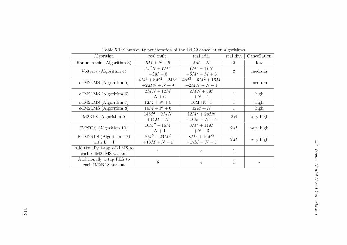
5.4W
iener
Mod
elB
asedC
ancellation
Table 5.1: Complexity per iteration of the IMD2 cancellation algorithms
Algorithm real mult. real add. real div. Cancellation
Hammerstein (Algorithm 3) 5M +N + 5 5M +N 2 low
Volterra (Algorithm 4)M2N + 7M2
−2M + 6
(M2 − 1
)N
+6M2 −M + 32 medium
ε-IM2LMS (Algorithm 5)4M3 + 8M2 + 24M
+2MN +N + 94M3 + 6M2 + 16M
+2MN +N − 11 medium
ε-IM2LMS (Algorithm 6)2MN + 12M
+N + 62MN + 8M
+N − 11 high
ε-IM2LMS (Algorithm 7) 12M +N + 5 10M+N+1 1 high
ε-IM2LMS (Algorithm 8) 16M +N + 6 12M +N 1 high
IM2RLS (Algorithm 9)14M2 + 2MN
+14M +N12M2 + 2MN+10M +N − 5
2M very high
IM2RLS (Algorithm 10)10M2 + 18M
+N + 18M2 + 14M
+N − 32M very high
R-IM2RLS (Algorithm 12)with L = I
8M3 + 26M2
+18M +N + 18M3 + 16M2
+17M +N − 32M very high
Additionally 1-tap ε-NLMS toeach ε-IM2LMS variant
4 3 1 -
Additionally 1-tap RLS toeach IM2RLS variant
6 4 1 -
113
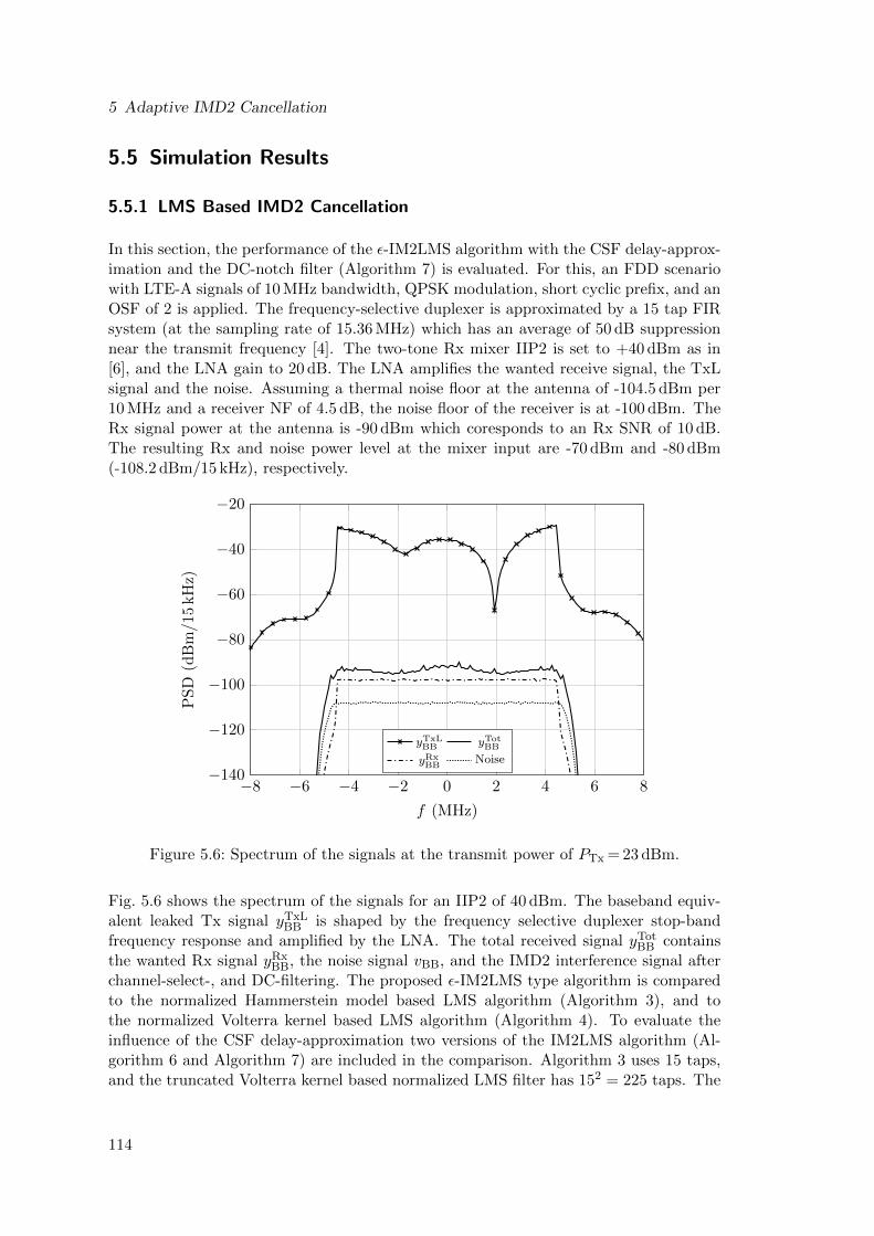
5 Adaptive IMD2 Cancellation
5.5 Simulation Results
5.5.1 LMS Based IMD2 Cancellation
In this section, the performance of the ε-IM2LMS algorithm with the CSF delay-approx-imation and the DC-notch filter (Algorithm 7) is evaluated. For this, an FDD scenariowith LTE-A signals of 10 MHz bandwidth, QPSK modulation, short cyclic prefix, and anOSF of 2 is applied. The frequency-selective duplexer is approximated by a 15 tap FIRsystem (at the sampling rate of 15.36 MHz) which has an average of 50 dB suppressionnear the transmit frequency [4]. The two-tone Rx mixer IIP2 is set to +40 dBm as in[6], and the LNA gain to 20 dB. The LNA amplifies the wanted receive signal, the TxLsignal and the noise. Assuming a thermal noise floor at the antenna of -104.5 dBm per10 MHz and a receiver NF of 4.5 dB, the noise floor of the receiver is at -100 dBm. TheRx signal power at the antenna is -90 dBm which coresponds to an Rx SNR of 10 dB.The resulting Rx and noise power level at the mixer input are -70 dBm and -80 dBm(-108.2 dBm/15 kHz), respectively.
−8 −6 −4 −2 0 2 4 6 8−140
−120
−100
−80
−60
−40
−20
f (MHz)
PS
D(d
Bm
/15
kH
z)
yTxLBB yTot
BB
yRxBB
Noise
Figure 5.6: Spectrum of the signals at the transmit power of PTx = 23 dBm.
Fig. 5.6 shows the spectrum of the signals for an IIP2 of 40 dBm. The baseband equiv-alent leaked Tx signal yTxL
BB is shaped by the frequency selective duplexer stop-bandfrequency response and amplified by the LNA. The total received signal yTot
BB containsthe wanted Rx signal yRx
BB, the noise signal vBB, and the IMD2 interference signal afterchannel-select-, and DC-filtering. The proposed ε-IM2LMS type algorithm is comparedto the normalized Hammerstein model based LMS algorithm (Algorithm 3), and tothe normalized Volterra kernel based LMS algorithm (Algorithm 4). To evaluate theinfluence of the CSF delay-approximation two versions of the IM2LMS algorithm (Al-gorithm 6 and Algorithm 7) are included in the comparison. Algorithm 3 uses 15 taps,and the truncated Volterra kernel based normalized LMS filter has 152 = 225 taps. The
114
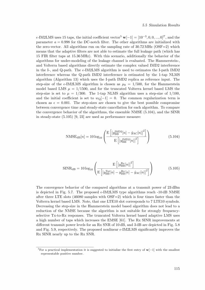
5.5 Simulation Results
ε-IM2LMS uses 15 taps, the initial coefficient vector5 w[−1] = [10−3, 0, 0, ..., 0]T , and theparameter a = 0.998 for the DC-notch filter. The other algorithms are initialized withthe zero-vector. All algorithms run on the sampling rate of 30.72 MHz (OSF=2) whichmeans that the adaptive filters are not able to estimate the full leakage path (which has15 FIR filter taps at 15.36 MHz). With this scenario, additionally the behavior of thealgorithms for under-modeling of the leakage channel is evaluated. The Hammerstein-,and Volterra based algorithms directly estimate the complex valued IMD2 interferencein the I-, and Q-path. The ε-IM2LMS algorithm is used to estimates the I-path IMD2interference whereas the Q-path IMD2 interference is estimated by the 1-tap NLMSalgorithm (Algorithm 13) which uses the I-path IMD2 replica as reference input. Thestep-size of the ε-IM2LMS algorithm is chosen as µ0 = 1/500, for the Hammersteinmodel based LMS µ = 1/1500, and for the truncated Volterra kernel based LMS thestep-size is set to µ = 1/300. The 1-tap NLMS algorithm uses a step-size of 1/100,and the initial coefficient is set to wQ[−1] = 0. The common regularization term ischosen as ε = 0.001. The step-sizes are chosen to give the best possible compromisebetween convergence time and steady-state cancellation for each algorithm. To comparethe convergence behavior of the algorithms, the ensemble NMSE (5.104), and the SINRin steady-state (5.105) [9, 23] are used as performance measure:
NMSEdB[n] = 10 log10
E[∣∣yIMD2
BB [n]− yAC[n]∣∣2]
E[∣∣yIMD2
BB [n]∣∣2]
(5.104)
SINRdB = 10 log10
E[∣∣yRx
BB[n]∣∣2]
E[∣∣yTot
BB [n]− yRxBB[n]− yAC[n]
∣∣2]
(5.105)
The convergence behavior of the compared algorithms at a transmit power of 23 dBmis depicted in Fig. 5.7. The proposed ε-IM2LMS type algorithms reach -10 dB NMSEafter three LTE slots (46080 samples with OSF=2) which is four times faster than theVolterra kernel based LMS. Note, that one LTE10 slot corresponds to 7 LTE10 symbols.Decreasing the step-size in the Hammerstein model based algorithm does not lead to areduction of the NMSE because the algorithm is not suitable for strongly frequency-selective Tx-to-Rx responses. The truncated Volterra kernel based adaptive LMS usesa high number of taps which increases the EMSE [61]. The Rx SINR improvements atdifferent transmit power levels for an Rx SNR of 10 dB, and 3 dB are depicted in Fig. 5.8and Fig. 5.9, respectively. The proposed nonlinear ε-IM2LMS significantly improves theRx SINR nearly up to the Rx SNR.
5For a practical implementation it is suggested to initialize the first entry of w[−1] with the smallestrepresentable positive number.
115
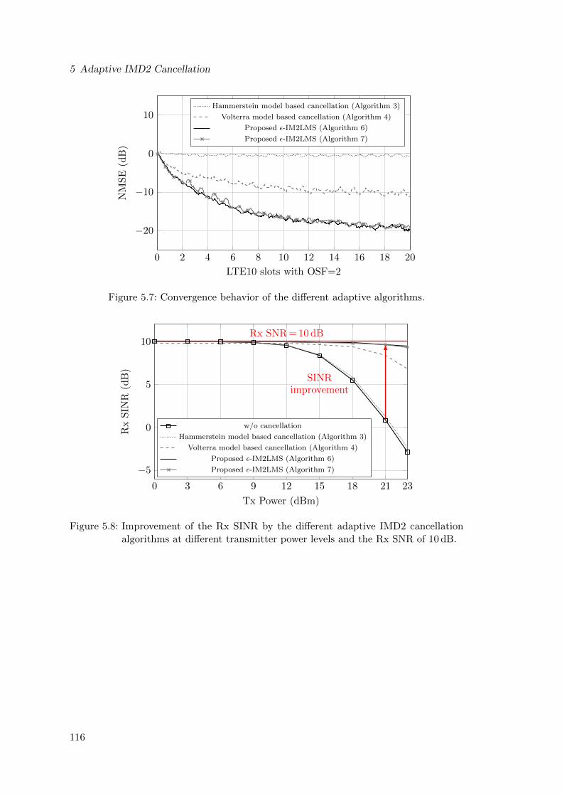
5 Adaptive IMD2 Cancellation
0 2 4 6 8 10 12 14 16 18 20
−20
−10
0
10
LTE10 slots with OSF=2
NM
SE
(dB
)
Hammerstein model based cancellation (Algorithm 3)
Volterra model based cancellation (Algorithm 4)
Proposed ε-IM2LMS (Algorithm 6)
Proposed ε-IM2LMS (Algorithm 7)
Figure 5.7: Convergence behavior of the different adaptive algorithms.
0 3 6 9 12 15 18 21 23
10
5
0
−5
SINRimprovement
Rx SNR = 10 dB
Tx Power (dBm)
Rx
SIN
R(d
B)
w/o cancellation
Hammerstein model based cancellation (Algorithm 3)
Volterra model based cancellation (Algorithm 4)
Proposed ε-IM2LMS (Algorithm 6)
Proposed ε-IM2LMS (Algorithm 7)
Figure 5.8: Improvement of the Rx SINR by the different adaptive IMD2 cancellationalgorithms at different transmitter power levels and the Rx SNR of 10 dB.
116
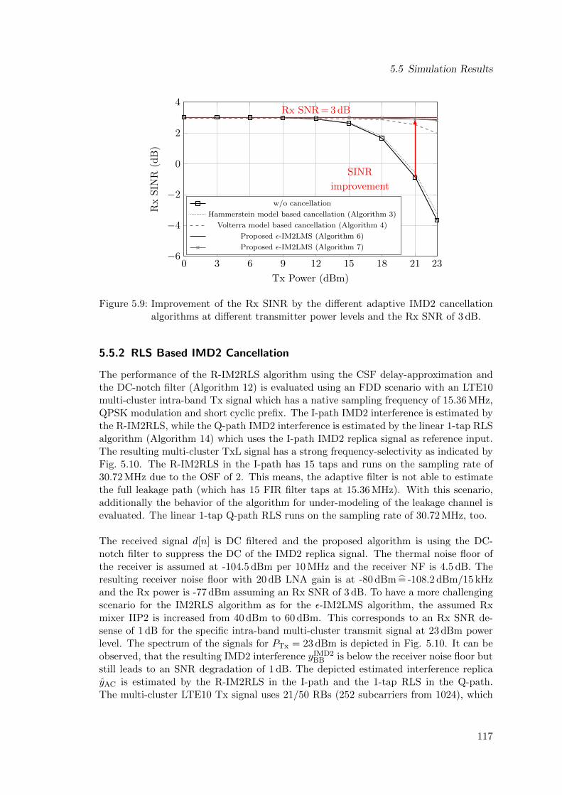
5.5 Simulation Results
0 3 6 9 12 15 18 21 23
4
2
0
−2
−4
−6
SINR
improvement
Rx SNR = 3 dB
Tx Power (dBm)
Rx
SIN
R(d
B)
w/o cancellation
Hammerstein model based cancellation (Algorithm 3)
Volterra model based cancellation (Algorithm 4)
Proposed ε-IM2LMS (Algorithm 6)
Proposed ε-IM2LMS (Algorithm 7)
Figure 5.9: Improvement of the Rx SINR by the different adaptive IMD2 cancellationalgorithms at different transmitter power levels and the Rx SNR of 3 dB.
5.5.2 RLS Based IMD2 Cancellation
The performance of the R-IM2RLS algorithm using the CSF delay-approximation andthe DC-notch filter (Algorithm 12) is evaluated using an FDD scenario with an LTE10multi-cluster intra-band Tx signal which has a native sampling frequency of 15.36 MHz,QPSK modulation and short cyclic prefix. The I-path IMD2 interference is estimated bythe R-IM2RLS, while the Q-path IMD2 interference is estimated by the linear 1-tap RLSalgorithm (Algorithm 14) which uses the I-path IMD2 replica signal as reference input.The resulting multi-cluster TxL signal has a strong frequency-selectivity as indicated byFig. 5.10. The R-IM2RLS in the I-path has 15 taps and runs on the sampling rate of30.72 MHz due to the OSF of 2. This means, the adaptive filter is not able to estimatethe full leakage path (which has 15 FIR filter taps at 15.36 MHz). With this scenario,additionally the behavior of the algorithm for under-modeling of the leakage channel isevaluated. The linear 1-tap Q-path RLS runs on the sampling rate of 30.72 MHz, too.
The received signal d[n] is DC filtered and the proposed algorithm is using the DC-notch filter to suppress the DC of the IMD2 replica signal. The thermal noise floor ofthe receiver is assumed at -104.5 dBm per 10 MHz and the receiver NF is 4.5 dB. Theresulting receiver noise floor with 20 dB LNA gain is at -80 dBm = -108.2 dBm/15 kHzand the Rx power is -77 dBm assuming an Rx SNR of 3 dB. To have a more challengingscenario for the IM2RLS algorithm as for the ε-IM2LMS algorithm, the assumed Rxmixer IIP2 is increased from 40 dBm to 60 dBm. This corresponds to an Rx SNR de-sense of 1 dB for the specific intra-band multi-cluster transmit signal at 23 dBm powerlevel. The spectrum of the signals for PTx = 23 dBm is depicted in Fig. 5.10. It can beobserved, that the resulting IMD2 interference yIMD2
BB is below the receiver noise floor butstill leads to an SNR degradation of 1 dB. The depicted estimated interference replicayAC is estimated by the R-IM2RLS in the I-path and the 1-tap RLS in the Q-path.The multi-cluster LTE10 Tx signal uses 21/50 RBs (252 subcarriers from 1024), which
117
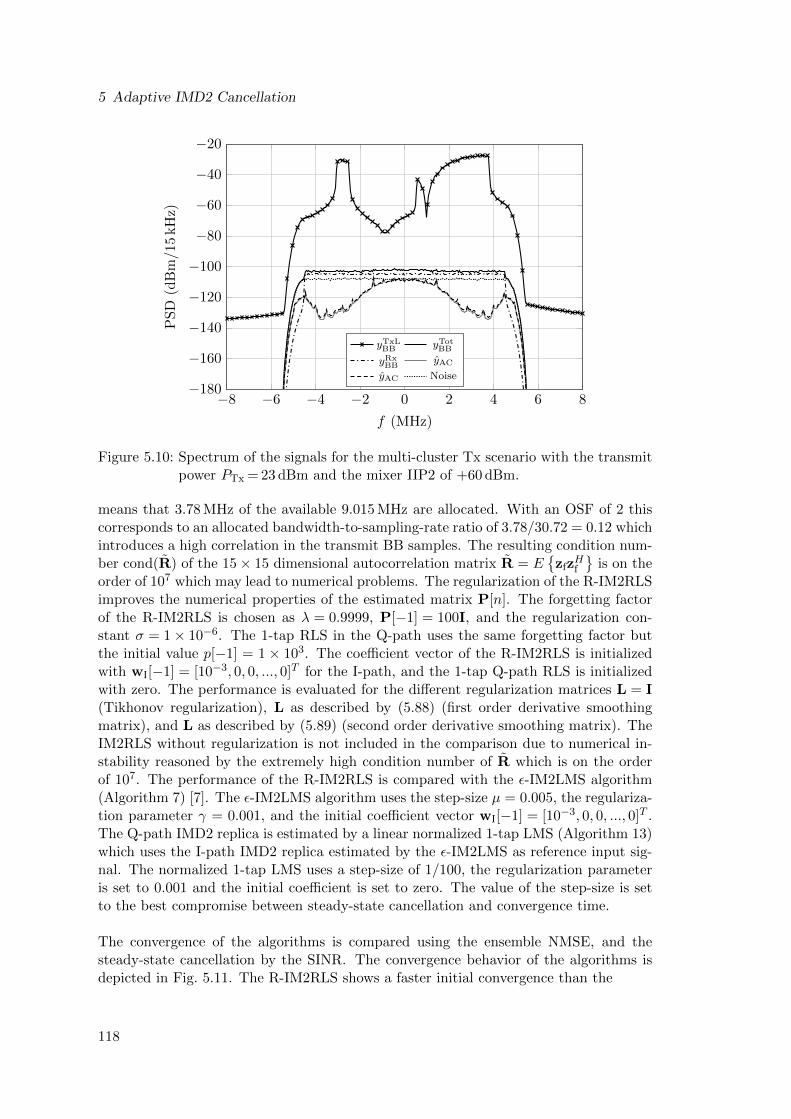
5 Adaptive IMD2 Cancellation
−8 −6 −4 −2 0 2 4 6 8−180
−160
−140
−120
−100
−80
−60
−40
−20
f (MHz)
PS
D(d
Bm
/15
kH
z)
yTxLBB yTot
BB
yRxBB
yAC
yAC Noise
Figure 5.10: Spectrum of the signals for the multi-cluster Tx scenario with the transmitpower PTx = 23 dBm and the mixer IIP2 of +60 dBm.
means that 3.78 MHz of the available 9.015 MHz are allocated. With an OSF of 2 thiscorresponds to an allocated bandwidth-to-sampling-rate ratio of 3.78/30.72 = 0.12 whichintroduces a high correlation in the transmit BB samples. The resulting condition num-ber cond(R) of the 15× 15 dimensional autocorrelation matrix R = E
zfz
Hf
is on the
order of 107 which may lead to numerical problems. The regularization of the R-IM2RLSimproves the numerical properties of the estimated matrix P[n]. The forgetting factorof the R-IM2RLS is chosen as λ = 0.9999, P[−1] = 100I, and the regularization con-stant σ = 1× 10⁻⁶. The 1-tap RLS in the Q-path uses the same forgetting factor butthe initial value p[−1] = 1 × 10³. The coefficient vector of the R-IM2RLS is initializedwith wI[−1] = [10−3, 0, 0, ..., 0]T for the I-path, and the 1-tap Q-path RLS is initializedwith zero. The performance is evaluated for the different regularization matrices L = I(Tikhonov regularization), L as described by (5.88) (first order derivative smoothingmatrix), and L as described by (5.89) (second order derivative smoothing matrix). TheIM2RLS without regularization is not included in the comparison due to numerical in-stability reasoned by the extremely high condition number of R which is on the orderof 107. The performance of the R-IM2RLS is compared with the ε-IM2LMS algorithm(Algorithm 7) [7]. The ε-IM2LMS algorithm uses the step-size µ = 0.005, the regulariza-tion parameter γ = 0.001, and the initial coefficient vector wI[−1] = [10−3, 0, 0, ..., 0]T .The Q-path IMD2 replica is estimated by a linear normalized 1-tap LMS (Algorithm 13)which uses the I-path IMD2 replica estimated by the ε-IM2LMS as reference input sig-nal. The normalized 1-tap LMS uses a step-size of 1/100, the regularization parameteris set to 0.001 and the initial coefficient is set to zero. The value of the step-size is setto the best compromise between steady-state cancellation and convergence time.
The convergence of the algorithms is compared using the ensemble NMSE, and thesteady-state cancellation by the SINR. The convergence behavior of the algorithms isdepicted in Fig. 5.11. The R-IM2RLS shows a faster initial convergence than the
118
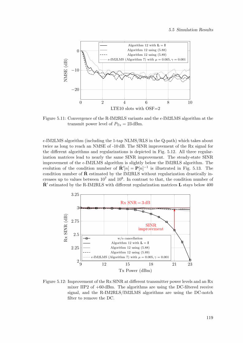
5.5 Simulation Results
0 2 4 6 8 10
−20
−10
0
LTE10 slots with OSF=2
NM
SE
(dB
)
Algorithm 12 with L = I
Algorithm 12 using (5.88)
Algorithm 12 using (5.89)
ε-IM2LMS (Algorithm 7) with µ = 0.005, γ = 0.001
Figure 5.11: Convergence of the R-IM2RLS variants and the ε-IM2LMS algorithm at thetransmit power level of PTx = 23 dBm.
ε-IM2LMS algorithm (including the 1-tap NLMS/RLS in the Q-path) which takes abouttwice as long to reach an NMSE of -10 dB. The SINR improvement of the Rx signal forthe different algorithms and regularizations is depicted in Fig. 5.12. All three regular-ization matrices lead to nearly the same SINR improvement. The steady-state SINRimprovement of the ε-IM2LMS algorithm is slightly below the IM2RLS algorithm. Theevolution of the condition number of R′[n] = P[n]−1 is illustrated in Fig. 5.13. Thecondition number of R estimated by the IM2RLS without regularization drastically in-creases up to values between 107 and 108. In contrast to that, the condition number ofR′ estimated by the R-IM2RLS with different regularization matrices L stays below 400
9 12 15 18 21 232
2.25
2.5
2.75
3
3.25
SINRimprovement
Rx SNR = 3 dB
Tx Power (dBm)
Rx
SIN
R(d
B)
w/o cancellation
Algorithm 12 with L = I
Algorithm 12 using (5.88)
Algorithm 12 using (5.89)
ε-IM2LMS (Algorithm 7) with µ = 0.005, γ = 0.001
Figure 5.12: Improvement of the Rx SINR at different transmitter power levels and an Rxmixer IIP2 of +60 dBm. The algorithms are using the DC-filtered receivesignal, and the R-IM2RLS/IM2LMS algorithms are using the DC-notchfilter to remove the DC.
119
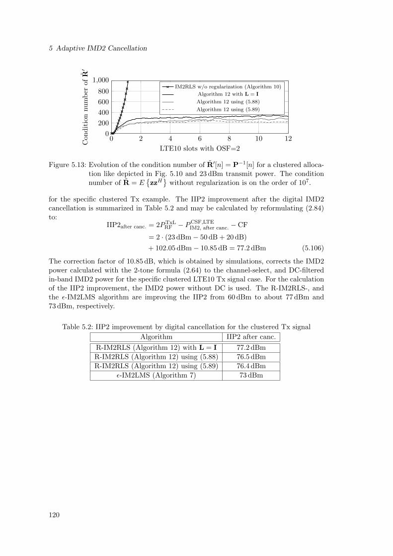
5 Adaptive IMD2 Cancellation
0 2 4 6 8 10 120
200
400
600
800
1,000
LTE10 slots with OSF=2
Con
dit
ion
nu
mb
erof
R′
IM2RLS w/o regularization (Algorithm 10)
Algorithm 12 with L = I
Algorithm 12 using (5.88)
Algorithm 12 using (5.89)
Figure 5.13: Evolution of the condition number of R′[n] = P−1[n] for a clustered alloca-tion like depicted in Fig. 5.10 and 23 dBm transmit power. The conditionnumber of R = E
zzH
without regularization is on the order of 107.
for the specific clustered Tx example. The IIP2 improvement after the digital IMD2cancellation is summarized in Table 5.2 and may be calculated by reformulating (2.84)to:
IIP2after canc. = 2PTxLRF − PCSF,LTE
IM2, after canc. − CF
= 2 · (23 dBm− 50 dB + 20 dB)
+ 102.05 dBm− 10.85 dB = 77.2 dBm (5.106)
The correction factor of 10.85 dB, which is obtained by simulations, corrects the IMD2power calculated with the 2-tone formula (2.64) to the channel-select, and DC-filteredin-band IMD2 power for the specific clustered LTE10 Tx signal case. For the calculationof the IIP2 improvement, the IMD2 power without DC is used. The R-IM2RLS-, andthe ε-IM2LMS algorithm are improving the IIP2 from 60 dBm to about 77 dBm and73 dBm, respectively.
Table 5.2: IIP2 improvement by digital cancellation for the clustered Tx signal
Algorithm IIP2 after canc.
R-IM2RLS (Algorithm 12) with L = I 77.2 dBm
R-IM2RLS (Algorithm 12) using (5.88) 76.5 dBm
R-IM2RLS (Algorithm 12) using (5.89) 76.4 dBm
ε-IM2LMS (Algorithm 7) 73 dBm
120
5.6 Verification with Measured Data
5.6 Verification with Measured Data
The developed Wiener model based IMD2 cancellation algorithms are also tested withmeasurement data. Two measurement scenarios are investigated. The first measurementsetup is based on a real RF transceiver chip provided by the industrial partner. Here,the TxL signal caused IMD2 self-interference is measured by the integrated IQ-receiverwhich includes 25% duty-cycle mixers. The following algorithms were evaluated withthe obtained measurement data:
Algorithm 6: ε-IM2LMS algorithm with DC-notch filter and CSF in the coefficientupdate.
Algorithm 7: Patented ε-IM2LMS algorithm with DC-notch filter and CSF delayapproximation.
Algorithm 8: ε-IM2LMS algorithm with simplified implicit DC cancellation andCSF delay approximation.
Algorithm 10: IM2RLS algorithm with DC-notch filter and CSF delay approxima-tion.
In this comparison, the performance of different versions of the ε-IM2LMS algorithm isevaluated in a real measurement scenario. It turns out, that all variants have nearly thesame IMD2 cancellation performance. Furthermore, their performance is compared tothe IM2RLS algorithm.
In the second scenario, a measurement setup consisting of discrete RF components (PA,LNA, mixer, duplexer) compared to the integrated RF chip in the first scenario is usedto generate the TxL signal caused IMD2 interference. In this scenario the followingalgorithms are evaluated:
Algorithm 7: Patented ε-IM2LMS algorithm with DC-notch filter and CSF delayapproximation.
Algorithm 12: R-IM2RLS algorithm with DC-notch filter and CSF delay approxi-mation.
In this scenario the performance of the R-IM2RLS algorithm is evaluated with measureddata and its performance is compared to the ε-IM2LMS algorithm. However, no multi-cluster Tx signal is used and therefore also the IM2RLS algorithm without regularizationis applicable in this scenario.
5.6.1 Measurements from the Transceiver Chip
The functionality of the derived ε-IM2LMS- and IM2RLS algorithm is demonstratedusing measured IQ data streams from a real transceiver chip which contain the IMD2interference. The mixers in the receiver are implemented as 25% duty-cycle current-driven passive mixers (see Section 2.2 for details). The transmitter within the trans-ceiver operated at fTx = 1856 MHz, and the receiver LO was set to fRx = 1936 MHzwhich corresponds to LTE band 2. The transceiver chip is mounted on an engine-board
121
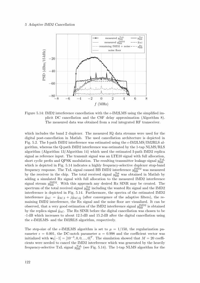
5 Adaptive IMD2 Cancellation
−8 −6 −4 −2 0 2 4 6 8−80
−60
−40
−20
f (MHz)
PS
D(d
Bm
/15
kH
z)
measured yTxLBB yTot
BB
measured yIMD2BB
yAC
remaining IMD2 + noise yRxBB
noise floor
Figure 5.14: IMD2 interference cancellation with the ε-IM2LMS using the simplified im-plicit DC cancellation and the CSF delay approximation (Algorithm 8).The measured data was obtained from a real integrated RF transceiver.
which includes the band 2 duplexer. The measured IQ data streams were used for thedigital post-cancellation in Matlab. The used cancellation architecture is depicted inFig. 5.2. The I-path IMD2 interference was estimated using the ε-IM2LMS/IM2RLS al-gorithm, whereas the Q-path IMD2 interference was estimated by the 1-tap NLMS/RLSalgorithm (Algorithm 13/Algorithm 14) which used the estimated I-path IMD2 replicasignal as reference input. The transmit signal was an LTE10 signal with full allocation,short cyclic prefix and QPSK modulation. The resulting transmitter leakage signal yTxL
BB
which is depicted in Fig. 5.14 indicates a highly frequency-selective duplexer stop-bandfrequency response. The TxL signal caused BB IMD2 interference yIMD2
BB was measuredby the receiver in the chip. The total received signal yTot
BB was obtained in Matlab byadding a simulated Rx signal with full allocation to the measured IMD2 interferencesignal stream yIMD2
BB . With this approach any desired Rx SINR may be created. Thespectrum of the total received signal yTot
BB including the wanted Rx signal and the IMD2interference is depicted in Fig. 5.14. Furthermore, the spectra of the estimated IMD2interference yAC = yAC,I + jyAC,Q (after convergence of the adaptive filters), the re-maining IMD2 interference, the Rx signal and the noise floor are visualized. It can beobserved, that a very good estimation of the IMD2 interference signal yIMD2
BB is obtainedby the replica signal yAC. The Rx SINR before the digital cancellation was chosen to be-1 dB which increases to about 12.5 dB and 15.2 dB after the digital cancellation usingthe ε-IM2LMS- and the IM2RLS algorithm, respectively.
The step-size of the ε-IM2LMS algorithm is set to µ = 1/150, the regularization pa-rameter ε = 0.001, the DC-notch parameter a = 0.998 and the coefficient vector wasinitialized with wI[−1] = [10−3, 0, 0, ..., 0]T . The simulation showed that M = 20 coeffi-cients were needed to cancel the IMD2 interference which was generated by the heavilyfrequency-selective TxL signal yTxL
BB (see Fig. 5.14). The 1-tap NLMS algorithm for the
122
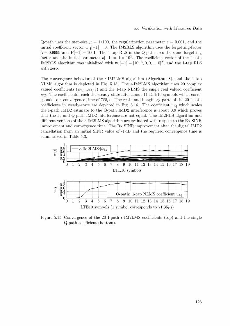
5.6 Verification with Measured Data
Q-path uses the step-size µ = 1/100, the regularization parameter ε = 0.001, and theinitial coefficient vector wQ[−1] = 0. The IM2RLS algorithm uses the forgetting-factorλ = 0.9999 and P[−1] = 100I. The 1-tap RLS in the Q-path uses the same forgettingfactor and the initial parameter p[−1] = 1 × 10³. The coefficient vector of the I-pathIM2RLS algorithm was initialized with wI[−1] = [10−3, 0, 0, ..., 0]T , and the 1-tap RLSwith zero.
The convergence behavior of the ε-IM2LMS algorithm (Algorithm 8), and the 1-tapNLMS algorithm is depicted in Fig. 5.15. The ε-IM2LMS algorithm uses 20 complexvalued coefficients (wI,0...wI,19) and the 1-tap NLMS the single real valued coefficientwQ. The coefficients reach the steady-state after about 11 LTE10 symbols which corre-sponds to a convergence time of 785µs. The real-, and imaginary parts of the 20 I-pathcoefficients in steady-state are depicted in Fig. 5.16. The coefficient wQ which scalesthe I-path IMD2 estimate to the Q-path IMD2 interference is about 0.9 which provesthat the I-, and Q-path IMD2 interference are not equal. The IM2RLS algorithm anddifferent versions of the ε-IM2LMS algorithm are evaluated with respect to the Rx SINRimprovement and convergence time. The Rx SINR improvement after the digital IMD2cancellation from an initial SINR value of -1 dB and the required convergence time issummarized in Table 5.3.
0 1 2 3 4 5 6 7 8 9 10 11 12 13 14 15 16 17 18 190
0.20.40.60.8
1
LTE10 symbols
|wI,i| ε-IM2LMS:|wI,i|
0 1 2 3 4 5 6 7 8 9 10 11 12 13 14 15 16 17 18 190
0.20.40.60.8
1
LTE10 symbols (1 symbol corresponds to 71.35µs)
wQ
Q-path: 1-tap NLMS coefficient wQ
Figure 5.15: Convergence of the 20 I-path ε-IM2LMS coefficients (top) and the singleQ-path coefficient (bottom).
123
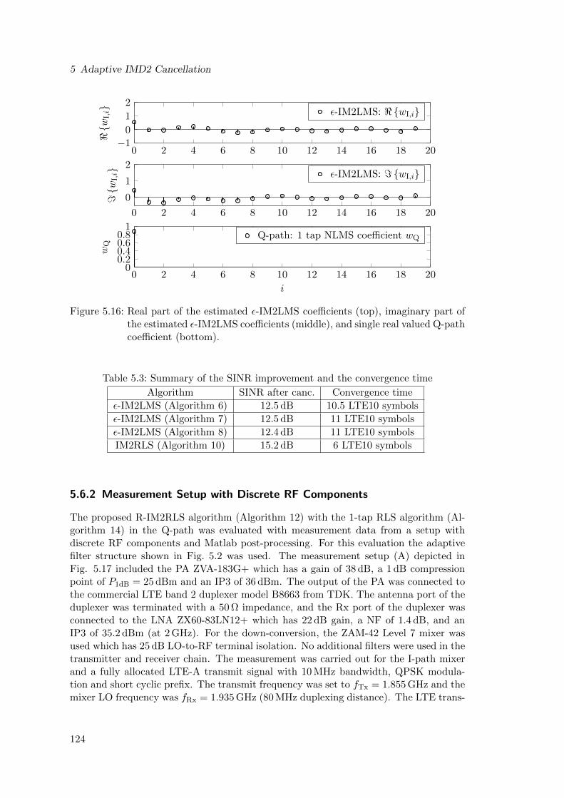
5 Adaptive IMD2 Cancellation
0 2 4 6 8 10 12 14 16 18 20−1
0
1
2<w
I,i ε-IM2LMS: <wI,i
0 2 4 6 8 10 12 14 16 18 20
0
1
2
=w
I,i ε-IM2LMS: =wI,i
0 2 4 6 8 10 12 14 16 18 200
0.20.40.60.8
1
i
wQ
Q-path: 1 tap NLMS coefficient wQ
Figure 5.16: Real part of the estimated ε-IM2LMS coefficients (top), imaginary part ofthe estimated ε-IM2LMS coefficients (middle), and single real valued Q-pathcoefficient (bottom).
Table 5.3: Summary of the SINR improvement and the convergence time
Algorithm SINR after canc. Convergence time
ε-IM2LMS (Algorithm 6) 12.5 dB 10.5 LTE10 symbols
ε-IM2LMS (Algorithm 7) 12.5 dB 11 LTE10 symbols
ε-IM2LMS (Algorithm 8) 12.4 dB 11 LTE10 symbols
IM2RLS (Algorithm 10) 15.2 dB 6 LTE10 symbols
5.6.2 Measurement Setup with Discrete RF Components
The proposed R-IM2RLS algorithm (Algorithm 12) with the 1-tap RLS algorithm (Al-gorithm 14) in the Q-path was evaluated with measurement data from a setup withdiscrete RF components and Matlab post-processing. For this evaluation the adaptivefilter structure shown in Fig. 5.2 was used. The measurement setup (A) depicted inFig. 5.17 included the PA ZVA-183G+ which has a gain of 38 dB, a 1 dB compressionpoint of P1dB = 25 dBm and an IP3 of 36 dBm. The output of the PA was connected tothe commercial LTE band 2 duplexer model B8663 from TDK. The antenna port of theduplexer was terminated with a 50 Ω impedance, and the Rx port of the duplexer wasconnected to the LNA ZX60-83LN12+ which has 22 dB gain, a NF of 1.4 dB, and anIP3 of 35.2 dBm (at 2 GHz). For the down-conversion, the ZAM-42 Level 7 mixer wasused which has 25 dB LO-to-RF terminal isolation. No additional filters were used in thetransmitter and receiver chain. The measurement was carried out for the I-path mixerand a fully allocated LTE-A transmit signal with 10 MHz bandwidth, QPSK modula-tion and short cyclic prefix. The transmit frequency was set to fTx = 1.855 GHz and themixer LO frequency was fRx = 1.935 GHz (80 MHz duplexing distance). The LTE trans-
124
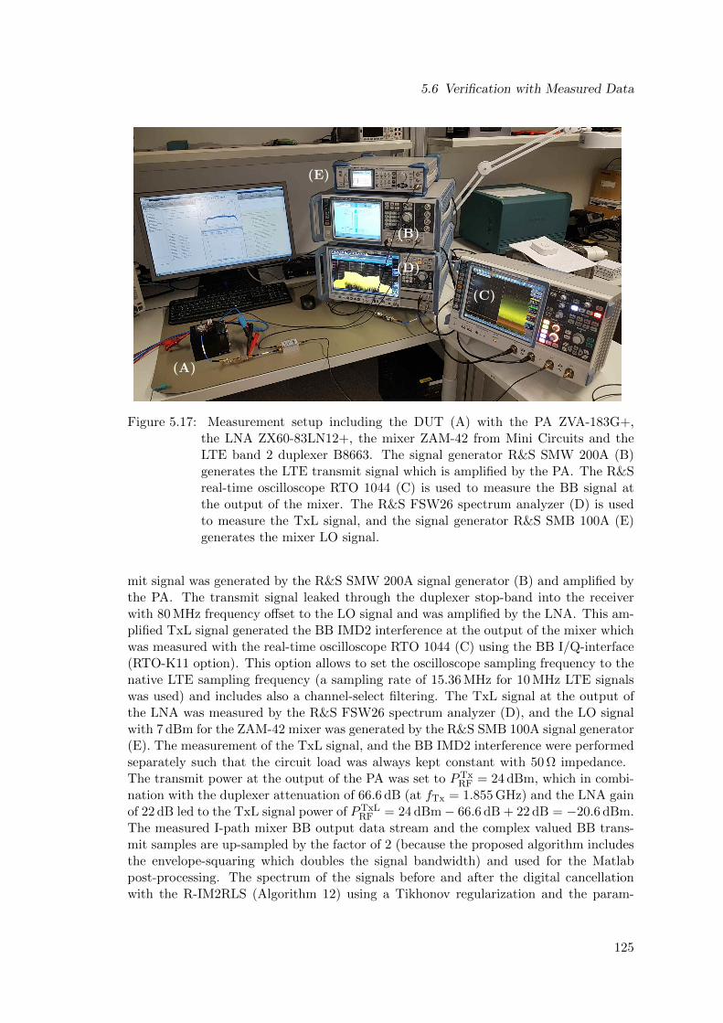
5.6 Verification with Measured Data
(E)
(B)
(C)
(A)
(D)
Figure 5.17: Measurement setup including the DUT (A) with the PA ZVA-183G+,the LNA ZX60-83LN12+, the mixer ZAM-42 from Mini Circuits and theLTE band 2 duplexer B8663. The signal generator R&S SMW 200A (B)generates the LTE transmit signal which is amplified by the PA. The R&Sreal-time oscilloscope RTO 1044 (C) is used to measure the BB signal atthe output of the mixer. The R&S FSW26 spectrum analyzer (D) is usedto measure the TxL signal, and the signal generator R&S SMB 100A (E)generates the mixer LO signal.
mit signal was generated by the R&S SMW 200A signal generator (B) and amplified bythe PA. The transmit signal leaked through the duplexer stop-band into the receiverwith 80 MHz frequency offset to the LO signal and was amplified by the LNA. This am-plified TxL signal generated the BB IMD2 interference at the output of the mixer whichwas measured with the real-time oscilloscope RTO 1044 (C) using the BB I/Q-interface(RTO-K11 option). This option allows to set the oscilloscope sampling frequency to thenative LTE sampling frequency (a sampling rate of 15.36 MHz for 10 MHz LTE signalswas used) and includes also a channel-select filtering. The TxL signal at the output ofthe LNA was measured by the R&S FSW26 spectrum analyzer (D), and the LO signalwith 7 dBm for the ZAM-42 mixer was generated by the R&S SMB 100A signal generator(E). The measurement of the TxL signal, and the BB IMD2 interference were performedseparately such that the circuit load was always kept constant with 50 Ω impedance.The transmit power at the output of the PA was set to PTx
RF = 24 dBm, which in combi-nation with the duplexer attenuation of 66.6 dB (at fTx = 1.855 GHz) and the LNA gainof 22 dB led to the TxL signal power of PTxL
RF = 24 dBm− 66.6 dB + 22 dB = −20.6 dBm.The measured I-path mixer BB output data stream and the complex valued BB trans-mit samples are up-sampled by the factor of 2 (because the proposed algorithm includesthe envelope-squaring which doubles the signal bandwidth) and used for the Matlabpost-processing. The spectrum of the signals before and after the digital cancellationwith the R-IM2RLS (Algorithm 12) using a Tikhonov regularization and the param-
125
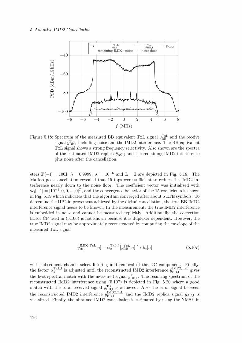
5 Adaptive IMD2 Cancellation
−8 −6 −4 −2 0 2 4 6 8
−100
−80
−60
−40
f (MHz)
PS
D(d
Bm
/15
kH
z)
yTxLBB yTot
BB,IyAC,I
remaining IMD2+noise noise floor
Figure 5.18: Spectrum of the measured BB equivalent TxL signal yTxLBB and the receive
signal yTotBB,I including noise and the IMD2 interference. The BB equivalent
TxL signal shows a strong frequency selectivity. Also shown are the spectraof the estimated IMD2 replica yAC,I and the remaining IMD2 interferenceplus noise after the cancellation.
eters P[−1] = 100I, λ = 0.9999, σ = 10−6 and L = I are depicted in Fig. 5.18. TheMatlab post-cancellation revealed that 15 taps were sufficient to reduce the IMD2 in-terference nearly down to the noise floor. The coefficient vector was initialized withwI[−1] = [10−3, 0, 0, ..., 0]T , and the convergence behavior of the 15 coefficients is shownin Fig. 5.19 which indicates that the algorithm converged after about 5 LTE symbols. Todetermine the IIP2 improvement achieved by the digital cancellation, the true BB IMD2interference signal needs to be known. In the measurement, the true IMD2 interferenceis embedded in noise and cannot be measured explicitly. Additionally, the correctionfactor CF used in (5.106) is not known because it is duplexer dependent. However, thetrue IMD2 signal may be approximately reconstructed by computing the envelope of themeasured TxL signal
yIMD2,TxLBB,I [n] = αTxL,I
2
∣∣yTxLBB [n]
∣∣2 ∗ hs[n] (5.107)
with subsequent channel-select filtering and removal of the DC component. Finally,the factor αTxL,I
2 is adjusted until the reconstructed IMD2 interference yIMD2,TxLBB,I gives
the best spectral match with the measured signal yTotBB,I. The resulting spectrum of the
reconstructed IMD2 interference using (5.107) is depicted in Fig. 5.20 where a goodmatch with the total received signal yTot
BB,I is achieved. Also the error signal between
the reconstructed IMD2 interference yIMD2,TxLBB,I and the IMD2 replica signal yAC,I is
visualized. Finally, the obtained IMD2 cancellation is estimated by using the NMSE in
126
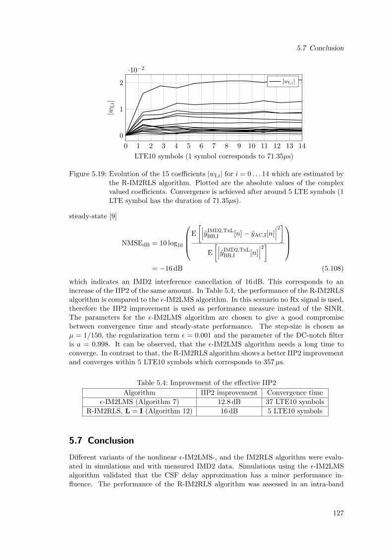
5.7 Conclusion
0 1 2 3 4 5 6 7 8 9 10 11 12 13 14
0
1
2
·10−2
LTE10 symbols (1 symbol corresponds to 71.35µs)
|wI,i|
∣∣wI,i
∣∣
Figure 5.19: Evolution of the 15 coefficients |wI,i| for i = 0 . . . 14 which are estimated bythe R-IM2RLS algorithm. Plotted are the absolute values of the complexvalued coefficients. Convergence is achieved after around 5 LTE symbols (1LTE symbol has the duration of 71.35µs).
steady-state [9]
NMSEdB = 10 log10
E
[∣∣∣yIMD2,TxLBB,I [n]− yAC,I[n]
∣∣∣2]
E
[∣∣∣yIMD2,TxLBB,I [n]
∣∣∣2]
= −16 dB (5.108)
which indicates an IMD2 interference cancellation of 16 dB. This corresponds to anincrease of the IIP2 of the same amount. In Table 5.4, the performance of the R-IM2RLSalgorithm is compared to the ε-IM2LMS algorithm. In this scenario no Rx signal is used,therefore the IIP2 improvement is used as performance measure instead of the SINR.The parameters for the ε-IM2LMS algorithm are chosen to give a good compromisebetween convergence time and steady-state performance. The step-size is chosen asµ = 1/150, the regularization term ε = 0.001 and the parameter of the DC-notch filteris a = 0.998. It can be observed, that the ε-IM2LMS algorithm needs a long time toconverge. In contrast to that, the R-IM2RLS algorithm shows a better IIP2 improvementand converges within 5 LTE10 symbols which corresponds to 357µs.
Table 5.4: Improvement of the effective IIP2
Algorithm IIP2 improvement Convergence time
ε-IM2LMS (Algorithm 7) 12.8 dB 37 LTE10 symbols
R-IM2RLS, L = I (Algorithm 12) 16 dB 5 LTE10 symbols
5.7 Conclusion
Different variants of the nonlinear ε-IM2LMS-, and the IM2RLS algorithm were evalu-ated in simulations and with measured IMD2 data. Simulations using the ε-IM2LMSalgorithm validated that the CSF delay approximation has a minor performance in-fluence. The performance of the R-IM2RLS algorithm was assessed in an intra-band
127
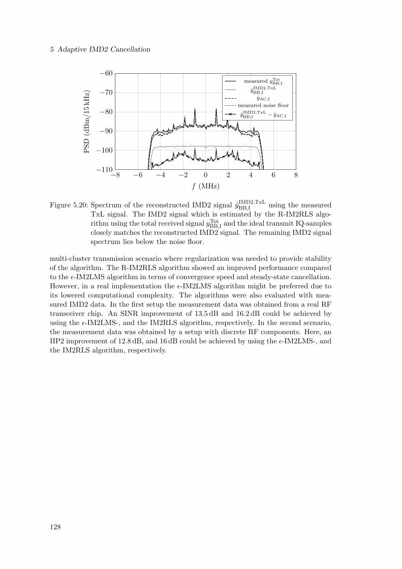
5 Adaptive IMD2 Cancellation
−8 −6 −4 −2 0 2 4 6 8−110
−100
−90
−80
−70
−60
f (MHz)
PS
D(d
Bm
/15
kH
z)measured yTot
BB,I
yIMD2,TxLBB,I
yAC,I
measured noise floor
yIMD2,TxLBB,I − yAC,I
Figure 5.20: Spectrum of the reconstructed IMD2 signal yIMD2,TxLBB,I using the measured
TxL signal. The IMD2 signal which is estimated by the R-IM2RLS algo-rithm using the total received signal yTot
BB,I and the ideal transmit IQ-samplesclosely matches the reconstructed IMD2 signal. The remaining IMD2 signalspectrum lies below the noise floor.
multi-cluster transmission scenario where regularization was needed to provide stabilityof the algorithm. The R-IM2RLS algorithm showed an improved performance comparedto the ε-IM2LMS algorithm in terms of convergence speed and steady-state cancellation.However, in a real implementation the ε-IM2LMS algorithm might be preferred due toits lowered computational complexity. The algorithms were also evaluated with mea-sured IMD2 data. In the first setup the measurement data was obtained from a real RFtransceiver chip. An SINR improvement of 13.5 dB and 16.2 dB could be achieved byusing the ε-IM2LMS-, and the IM2RLS algorithm, respectively. In the second scenario,the measurement data was obtained by a setup with discrete RF components. Here, anIIP2 improvement of 12.8 dB, and 16 dB could be achieved by using the ε-IM2LMS-, andthe IM2RLS algorithm, respectively.
128
6Conclusion and Outlook
In this thesis, two main receiver desensitization effects have been addressed. The firsteffect occurs in FDD transceivers, where a part of the transmit signal leaks into thereceiver and causes a receiver self-interference. The second effect is the harmonic down-conversion of blocker signals due to the harmonic response of the receive mixers whichare implemented as square-wave mixers. To be able to find countermeasures for bothtypes of receiver interferences, a detailed modeling of the TxL signal caused receiver self-interferences and also the used 25% duty-cycle current-driven passive mixers is providedin this thesis.
In this work, the receiver self-interference which is caused by the TxL signal is miti-gated by adaptive filtering in the digital BB. For this purpose, the mathematical modelsof several linear and nonlinear receiver interferences have been derived. The adaptivefiltering sections in this thesis focus on the digital cancellation of the modulated spur-,and the IMD2 interference. The modulated spur interference may be generated by LO-LO cross-talk in inter-band CA or also in intra-band CA scenarios where a split-LNAis used. For both cases the modulated spur interference may consist of a main and animage interference part. The derived widely-linear adaptive filter structure to cancel themain and the image modulated spur interference can be used in both cases. In this workthe cancellation of the modulated spur interference was demonstrated by simulations,and the results were published in [9]. The performance of four different adaptive algo-rithms was compared and it turns out that the ε-VSSNLMS algorithm represents thebest compromise regarding performance and computational complexity.
The main focus of this thesis is the pure digital cancellation of the IMD2 interfer-ence which is generated by the second-order nonlinearity of the Rx mixer. TraditionalVolterra kernel based approaches to cancel the IMD2 interference suffer from a highcomputational complexity of order O(M2) for LMS based algorithms and O(M4) forRLS based algorithms, respectively. This thesis presented novel nonlinear Wiener modelLMS-, and RLS based algorithms to cancel the IMD2 interference in the digital BB.The computational complexity of the proposed algorithms is O(M) and O(M2) for theLMS-, and the RLS algorithm based cancellation, respectively. The Wiener model usesa static nonlinearity at the output of the adaptive filter which has the advantage thatless coefficients are necessary in the estimation process compared to a Volterra kernelbased adaptive filter. The proposed ε-IM2LMS algorithm is a nonlinear normalized andregularized LMS based algorithm. For the IM2RLS algorithm also a regularized versionwas derived (R-IM2RLS) which is applicable for highly correlated transmit signals likeused in LTE multi-cluster transmissions. Both algorithms are able to estimate the IMD2interference in case of a highly frequency-selective Tx-to-Rx frequency responses. The
129
6 Conclusion and Outlook
performance of the algorithms was demonstrated by simulations with different Rx SNRscenarios, and both algorithms outperformed the traditional Volterra kernel LMS basedapproach in terms of adaptation speed and cancellation performance.
The performance of the Wiener model based algorithms was also demonstrated usingmeasurement data. In the first setup the measurement data was obtained from a realintegrated RF transceiver chip which is developed and manufactured by the industrialpartner. The proposed ε-IM2LMS algorithm and the R-IM2RLS algorithm were ableto improve the Rx SINR from -1 dB up to 12.5 dB and 15.2 dB, respectively. The co-efficients of the ε-IM2LMS algorithm converged after 11 LTE10 symbols whereas theR-IM2RLS algorithm needed only 6 LTE10 symbols. The second measurement setupincluded discrete RF components. Here, the mixer IIP2 could be increased by 12.8 dBand 16 dB with the ε-IM2LMS-, and the R-IM2RLS algorithm, respectively. The pre-sented ε-IM2LMS algorithm was patented by the industrial partner and resulted in theU.S. patent US 2018/015417 which was filed in June 2017. The derivation and the per-formance evaluation of the ε-IM2LMS-, and the R-IM2RLS algorithm were published in[7], and [27], respectively.
The square-wave mixer implementation in the receiver causes harmonics in the transis-tor control signals. This leads to a harmonic response of the mixer which down-convertsunwanted spectral components to the BB. Consequently, the reception of the wanted Rxsignal is degraded. In this thesis, a harmonic rejection concept to reject specific harmon-ics in the control signal of the 25% duty-cycle current driven passive mixer was presented.The proposed control scheme was implemented in a Cadence circuit simulation using theVirtuoso platform and a 28 nm technology package. The proposed harmonic rejectionapproach showed a superior suppression of the harmonic mixer response. The developedHR mixer concept for 25% duty-cycle mixers was patented by the industrial partner andresulted in the U.S. patent US 9,935,722 B2 which was filed in June 2016 and grantedin March 2018. The generation of the HR control signals using digital-to-time convert-ers (DTCs) was also patented by the industrial partner and resulted in the U.S. patentUS 9,755,872 B1, which was filed in August 2016 and granted in September 2017.
Future investigations may contain the digital cancellation of Tx harmonics and of highereven-order intermodulation distortions as the IMD4-, and the IMD6 interference. Fur-thermore, in this thesis it is assumed that only one interference desensitizes the receiverat a certain time. Another obvious aspect to be addressed is therefore the investigationof optimum digital cancellation strategies for co-existing receiver interferences.
130
AAppendix
A.1 Power Spectral Density Plots
The PSDs in this thesis are plotted with respect to the signal power within a specificbandwidth e.g. dBm/15kHz. If the signal has a frequency-flat spectrum (which isapproximately true for LTE signals), then the magnitude value of one frequency binwith the bin spacing ∆f = 15 kHz may be calculated as
Pbin =PRx
B∆f
[W
15 kHz
]. (A.1)
Here PRx is the signal power, B the signal bandwidth (e.g. 9.015 MHz for LTE10) and∆f = fs/NFFT where fs is the sampling frequency and NFFT the number of FFT bins.The bin power in dBm/15 kHz is then
Pbin = 10 log10
(Pbin
1mW
) [dBm
15 kHz
]. (A.2)
A.2 Spur Generation in 25% Duty-Cycle Mixers with theSplit-LNA Configuration
The Fourier coefficients of the I+ control signal in the 25% duty-cycle mixer with thepulse width jitter 2δ, and the LO phase offset ϕLO are
ck =1
TLO
∫ TLO
0pI+(t)e−jk(2πfLOt+ϕLO)dt
=1
TLO
∫ TLO/4+δ
−δAe−jk(2πfLOt+ϕLO)dt
=−Ajk2π
[e−jk(2πfLOt+ϕLO)
]∣∣∣∣TLO
4+δ
−δ
=−Ajk2π
[e−jk
(2πfLO
(TLO
4+δ
)+ϕLO
)− ejk(2πfLOδ−ϕLO)
]
=A
kπe−jk(
π4
+ϕLO) 1
2j
[ejk(
π4
+2πfLOδ) − e−jk(π4 +2πfLOδ)]
=A
kπe−jk(
π4
+ϕLO)sin
(kπ
4+ k2π
δ
TLO
)
= A
[1
4+ 2
δ
TLO
]e−jk
π4 sinc
(kπ
4+ k2π
δ
TLO
)e−jkϕLO ,
(A.3)
131
A Appendix
and allowing slow variations of δ and ϕ compared to fLO, the Fourier coefficients includ-ing amplitude- and phase-noise may be expressed as
ck(t) = A
[1
4+ 2
δ(t)
TLO
]e−jk
π4 sinc
(kπ
4+ k2π
δ(t)
TLO
)e−jkϕLO(t). (A.4)
By using c′k(t) = A[
14 + 2 δ(t)TLO
]sinc
(k π4 + k2π δ(t)
TLO
), the coefficients ck(t) may be rewrit-
ten as ck(t) = c′k(t)e−jk π
4 e−jkϕLO(t). The resulting model for the four mixer phasesI+,I-,Q+ and Q- of the first 25 % duty-cycle IQ-mixer (aggressor) including amplitude-,and phase-noise becomes [29]
pLO1,I+(t) =∞∑
m1=−∞am1(t)ejm12πfLO1
t(A.5)
pLO1,I-(t) =∞∑
m1=−∞(−1)m1am1(t)ejm12πfLO1
t(A.6)
pLO1,Q+(t) =∞∑
m1=−∞e−jm1
π2 am1(t)ejm12πfLO1
t(A.7)
pLO1,Q-(t) =∞∑
m1=−∞ejm1
π2 am1(t)ejm12πfLO1
t. (A.8)
The control signals of the second mixer (victim) are
pLO2,I+(t) =∞∑
m2=−∞bm2(t)ejm22πfLO2
t(A.9)
pLO2,I-(t) =∞∑
m2=−∞(−1)m2bm2(t)ejm22πfLO2
t(A.10)
pLO2,Q+(t) =∞∑
m2=−∞e−jm2
π2 bm2(t)ejm22πfLO2
t(A.11)
pLO2,Q-(t) =∞∑
m2=−∞ejm2
π2 bm2(t)ejm22πfLO2
t, (A.12)
where am1 and bm2 are the Fourier coefficients (A.4) of the first (LO1) and second (LO2)mixer, respectively. In the following spur model it is assumed, that each of the four mixercontrol signals of LO1 (aggressor) couples to each of the four phases of LO2 (victim).This corresponds to 16 coupling paths as depicted in Fig. 2.13. The resulting spurcurrent in the victim mixer LO2 generated by a coupling between the second harmonicof LO1 (m1 = ±2), and the fundamental of LO2 (m2 = ±1) becomes
iLO2RF,I+(t) = iTxL
RF (t) [γI+I+pLO1,I+(t) + γI-I+pLO1,I-(t) + γQ+I+pLO1,Q+(t)
+γQ-I+pLO1,Q-(t)] pLO2,I+(t)
= iTxLRF (t)
[γI+I+
(a2(t)ej2ω1t + a∗2(t)e−j2ω1t
)+ γI-I+
(a2(t)ej2ω1t + a∗2(t)e−j2ω1t
)
+γQ+I+
(a2(t)e−jπej2ω1t + a∗2(t)ejπe−j2ω1t
)
+γQ-I+
(a2(t)ejπej2ω1t + a∗2(t)e−jπe−j2ω1t
)]·(b1(t)ejω2t + b∗1(t)e−jω2t
),
(A.13)
132
A.2 Spur Generation in 25% Duty-Cycle Mixers with the Split-LNA Configuration
where ωLO1 = 2πfLO1 , ωLO2 = 2πfLO2 and γ is the coupling coefficient between the mixerbranches. E.g. γI-I+ is the coupling coefficient from the I- phase of LO1 to the I+ phaseof LO2. By defining ωsp = 2ωLO1 − ωLO2 , the current in the I+ branch of LO2 becomes
iLO2RF,I+(t) = iTxL
RF (t) [γI+I+ + γI-I+ − γQ+I+ − γQ-I+](a2(t)b∗1(t)ejωspt + a∗2(t)b1(t)e−j2ωspt
)
= 2iTxLRF (t) [γI+I+ + γI-I+ − γQ+I+ − γQ-I+]
· a′2(t)b′1(t)cos(ωspt− 2ϕLO1(t) + ϕLO2(t)− π
4
).
(A.14)The I- branch current becomes
iLO2RF,I-(t) = iTxL
RF (t) [γI+I-pLO1,I+(t) + γI-I-pLO1,I-(t) + γQ+I-pLO1,Q+(t)
+γQ-I-pLO1,Q-(t)] pLO2,I-(t)
= −2iTxLRF (t) [γI+I- + γI-I- − γQ+I- − γQ-I-]
· a′2(t)b′1(t)cos(ωspt− 2ϕLO1(t) + ϕLO2(t)− π
4
),
(A.15)
and the resulting differential spur current in the I-phase results in
iLO2RF,I(t) = iLO2
RF,I+(t)− iLO2RF,I-(t)
= 2iTxLRF (t)
γI+I+ + γI-I+ − γQ+I+ − γQ-I+ + γI+I- + γI-I- − γQ+I- − γQ-I-︸ ︷︷ ︸
γI
· a′2(t)b′1(t)cos(ωspt− 2ϕLO1(t) + ϕLO2(t)− π
4
).
(A.16)Similarly, the currents in the Q-branch are
iLO2RF,Q+(t) = iTxL
RF (t) [γI+Q+pLO1,I+(t) + γI-Q+pLO1,I-(t) + γQ+Q+pLO1,Q+(t)
+γQ-Q+pLO1,Q-(t)] pLO2,Q+(t)
= −2iTxLRF (t) [γI+Q+ + γI-Q+ − γQ+Q+ − γQ-Q+]
· a′2(t)b′1(t)sin(ωspt− 2ϕLO1(t) + ϕLO2(t)− π
4
),
(A.17)
and
iLO2RF,Q-(t) = iTxL
RF (t) [γI+Q-pLO1,I+(t) + γI-Q-pLO1,I-(t) + γQ+Q-pLO1,Q+(t)
+γQ-Q-pLO1,Q-(t)] pLO2,Q-(t)
= −2iTxLRF (t) [γI+Q- + γI-Q- − γQ+Q- − γQ-Q-]
· a′2(t)b′1(t)sin(ωspt− 2ϕLO1(t) + ϕLO2(t)− π
4
),
(A.18)
which leads to the differential spur current in the Q-path
iLO2RF,Q(t) = − (iRF,Q+(t)− iRF,Q-(t))
= −2iTxLRF (t)γQa
′2(t)b′1(t)sin
(ωspt− 2ϕLO1(t) + ϕLO2(t)− π
4
),
(A.19)
133
A Appendix
where γQ = −γI+Q+ − γI-Q- + γQ+Q+ + γQ-Q+ + γI+Q- + γI-Q- − γQ+Q- − γQ-Q-. The trans-mitter leakage signal creates the LNA output current iTxL
RF (t) which is first mixed by theaggressor LO1 and subsequently mixed by the victim LO2. Combining these mixingprocesses with the I-, and Q-component of the complex valued spur, the complex RFcurrent in the victim LO2 results in
iLO2RF (t) = iLO2
RF,I(t) + jiLO2RF,Q(t)
= 2 iTxLRF (t)a′2(t)b′1(t)
[γI cos
(ωspt− 2ϕLO1(t) + ϕLO2(t)− π
4
)
−jγQ sin(ωspt− 2ϕLO1(t) + ϕLO2(t)− π
4
)],
(A.20)
and with the identities, cos(ϕ) = 12
(ejϕ + e−jϕ
)and sin(ϕ) = 1
2j
(ejϕ − e−jϕ
)the current
becomes
iLO2RF (t) = 2 iTxL
RF (t)a′2(t)b′1(t)
·
γI + γQ
2︸ ︷︷ ︸K1
e−j(ωspt−2ϕLO1(t)+ϕLO2
(t)−π4 ) +
γI − γQ
2︸ ︷︷ ︸K2
ej(ωspt−2ϕLO1(t)+ϕLO2
(t)−π4 )
= 2 iTxLRF (t)
[K1a
∗2(t)b1(t)e−jωspt +K2a2(t)b∗1(t)ejωspt
]
= 2<iTxLBB (t)ejωTxt
[K1a
∗2(t)b
(1t)e
−jωspt +K2a2(t)b∗1(t)ejωspt]
=[iTxLBB (t)ejωTxt + iTxL*
BB (t)e−jωTxt]
·[K1a
∗2(t)b1(t)e−jωspt +K2a2(t)b∗1(t)ejωspt
]︸ ︷︷ ︸
psp(t)
.
(A.21)It can be observed, that the spur has a gain imbalance if γI 6= γQ which results in a mainand image signal component. The BB spur voltage with f∆ = fTx − fsp after low-passfiltering with the BB impedance zBB(t) becomes
uLO2BB (t) = iLO2
RF (t) ∗ zBB
=[K1a
∗2(t)b1(t)iTxL
BB (t)ej2πf∆t +K2a2(t)b∗1(t)iTxL*BB (t)e−j2πf∆t
]ZBB.
(A.22)
which shows that the modulated spur interference has a main and image component.
A.3 Receiver Noise Floor
The thermal in-band noise floor within the CSF pass-band bandwidth for LTE10 signalswith 9.015 MHz bandwidth may be calculated by
Pth,dBm = 10 log10
kTB
1mW
= 10 log10
1.38 10−23m2kg s−2K−1 · 323K · 9.015 MHz
1mW= −104 dBm,
(A.23)
where k = 1.3810−23m2kg s−2K−1 is the Boltzmann constant, T = 323K the temperaturein Kelvin (50celsius), and B the bandwidth. To the thermal noise floor, the receiver
134

A.4 Scaling of Complex Baseband Signals for a Desired Power Level, SNR and SINR
NF which is the noise contribution of the front-end circuit components (e.g. LNA) isadded. A typical value for the NF is 5 dB which results in the receiver noise floor
Pn,dBm = Pth,dBm + NF = −104 dBm + 5 dBm = −99 dBm. (A.24)
A.4 Scaling of Complex Baseband Signals for a Desired PowerLevel, SNR and SINR
A.4.1 Complex White Gaussian Noise
To generate a zero mean complex white Gaussian noise (CWGN) sequence
z[n] = x[n] + jy[n], n = 1...N
with the desired power Pn at the network impedance Z0, it is necessary to derive thevariance
σ2z = E (z[n]− µz) (z[n]− µz)∗ = E
x2[n] + y2[n]
= Ex2[n]
+ E
y2[n]
, for µz = 0
(A.25)
of the complex valued sequence. The real and the imaginary part of z[n] have the samepower, therefore
Ex2[n]
= E
y2[n]
holds, and the power becomes
Pn =E (z[n]− µz) (z[n]− µz)∗
Z0=
2Ex2[n]
Z0=
2σ2x
Z0.
Consequently, the standard deviation of the random variables x and y are given with
σx = σy =
√PnZ0
2
% Matlab code to generate a zero mean complex Gaussian distributed random ...vector with power Pn at the impedance Z0
z = sqrt(Pn Z0/2)*(randn(1,N)+j*randn(1,N));
A.4.2 Generation of an Rx Signal with Desired Power Level
It is assumed that a complex valued zero-mean discrete-time Rx signal yRxBB[n] is already
generated in Matlab which shall be scaled for the desired power level P desRx,dBm. The
actual power level of the signal is
PRx =E∣∣yRx
BB[n]∣∣2
Z0
(A.26)
assuming the network impedance of Z0. The desired power in linear scaling is
P desRx = 1 mW · 10
PdesRx,dBm
10 (A.27)
135

A Appendix
and by solving the equation
P desRx
!=
1
Z0
1
N
∑
n
∣∣k · yRxBB[n]
∣∣2 (A.28)
the scaling factor
k =
√P des
Rx
PRx
(A.29)
is obtained. The resulting Rx signal with the desired power becomes
yRx,desBB [n] = k · yRx
BB[n]. (A.30)
A.4.3 Generation of an Rx Signal with Desired SNR
The complex valued and zero-mean Rx signal which has the desired power PRx shall bedegraded by a band-limited noise signal resulting in the desired SNRdB. The SNR indecibel is
SNRdB = 10 log10
PRx
P desn
, (A.31)
and therefore the desired noise power is
P desn =
PRx
10SNRdB/10. (A.32)
A complex valued AWGN signal v′[n] is generated and filtered by the CSF with impulseresponse hs[n] to generate the band-limited noise vBB[n] = v′[n] ∗ hs[n] with the actualpower Pn. This band-limited noise signal has to be scaled correctly with the factor k toobtain the desired Rx SNR by solving
P desn
!=
1
Z0
1
N
∑
n
|k · vBB[n]|2 (A.33)
which results in
k =
√P des
n
Pn. (A.34)
The noise signal with the desired power is finally obtained with the scaling
vdesBB[n] = k · vBB[n]. (A.35)
A.4.4 Generation of an Rx Signal with Desired SINR
The scaling of the zero mean complex valued interference signal may be of interest whenthe interference is generated through systems with different frequency responses (e.g.duplexer impulse responses with varying attenuation). To evaluate the performanceof the adaptive filter the interference power is normalized to the desired SINR to getcomparable results. The SINR in decibel with the interference power Pint of the discretetime interference signal iBB[n] is calculated by
SINRdB = 10 log10
(PRx
Pn + Pint
), (A.36)
136
A.5 Derivative of a Channel-Select Filtered Signal
where
Pint =E|iBB|2
Z0. (A.37)
When the noise power Pn is chosen for a desired Rx SNR, then the interference powerfor a desired SINR may be derived by
P desint = PRx · 10−
SINRdB10 − Pn. (A.38)
The scaling factor becomes
k =
√P des
int
Pint, (A.39)
and the scaled interference signal to obtain a desired SINR is
idesBB[n] = k · iBB[n]. (A.40)
A.5 Derivative of a Channel-Select Filtered Signal
In the derivation of the IM2LMS algorithm in Section 5.4.4, the derivative of the non-holomorphic expression s[n] =
[wT
(x[n]xH [n]−Rxx
)w∗]∗ hs[n] with respect to the
coefficient vector w∗ including the channel-select filtering appears in the cost function.In this derivation using the Wirtinger Calculus the CSF hs[n] is assumed as an FIR filter,and the unknown coefficient vector w which minimizes the cost function is assumed tobe deterministic and is therefore not time varying. Rewriting s[n] to
s[n] =
wT
(x[n]xH [n]−Rxx
)︸ ︷︷ ︸
=zT [n]
w∗
∗ hs[n]
= hs,0zT [n]w∗ + hs,1z
T [n− 1]w∗ + . . .+ hs,K−1zT [n−K + 1]w∗
=[hs,0 hs,1 · · · hs,K−1
]
zT [n]zT [n− 1]
...zT [n−K + 1]
w∗
=[hs,0, hs,1, · · · , hs,K−1
]
z0[n] z1[n] · · · zM−1[n]z0[n− 1] z1[n− 1] · · · zM−1[n− 1]
......
...z0[n−K + 1] z1[n−K + 1] · · · zM−1[n−K + 1]
w∗
(A.41)
137
A Appendix
where K is the length of the finite CSF impulse response, the derivative of s[n] usingthe Wirtinger Calculus becomes
[∂s
∂w∗
]T=
z0[n] z0[n− 1] · · · z0[n−K + 1]z1[n] z1[n− 1] · · · z1[n−K + 1]
......
...zM−1[n] zM−1[n− 1] · · · zM−1[n−K + 1]
hs,0hs,1
...hs,K−1
=
z0[n] ∗ hs[n]z1[n] ∗ hs[n]
...zM−1[n] ∗ hs[n]
= z[n] ∗ hs[n]
= zf[n]
=(y′[n]x∗[n]−RT
xxw)∗ hs[n]
(A.42)
where the scalar FIR filter output y′[n] = xT [n]w is used. Additionally in the derivationof the IM2RLS algorithm the reformulation
s[n] =(zT [n]w∗
)∗ hs[n]
=(zH [n]w
)∗ hs[n]
= hs,0zH [n]w + hs,1z
H [n− 1]w + hs,K−1zH [n−K + 1]w
=[hs,0 hs,1 · · · hs,K−1
]
zH [n]zH [n− 1]
...zH [n−K + 1]
w
(A.43)
sT [n] = wT[z∗[n] z∗[n− 1] · · · z∗[n−K + 1]
]
hs,0hs,1
...hs,K−1
= wT
z∗0 [n] z∗0 [n− 1] · · · z∗0 [n−K + 1]z∗1 [n] z∗1 [n− 1] · · · z∗1 [n−K + 1]
......
...z∗M−1[n] z∗M−1[n− 1] · · · z∗M−1[n−K + 1]
hs,0hs,1
...hs,K−1
= wT
z∗0 [n] ∗ hs[n]z∗1 [n] ∗ hs[n]
...z∗M−1[n] ∗ hs[n]
= wT
z∗0 [n]z∗1 [n]
...z∗M−1[n]
∗ hs[n]
= wT z∗[n] ∗ hs[n]
(A.44)
138

A.5 Derivative of a Channel-Select Filtered Signal
which leads to
s[n] =(zH [n] ∗ hs[n]
)w (A.45)
is used.
139


List of Abbreviations
AAF anti-aliasing-filter
ADC analog-to-digital converter
BB baseband
BW bandwidth
CA carrier aggregation
CC component carriers
CSF channel-select filter
CW continuous wave
CWGN complex white Gaussian noise
DAC digital-to-analog converter
DC direct-current
DCO digitally controlled oscillator
DFE digital front-end
DL downlink
DTC digital-to-time converter
EMSE excess mean-square-error
FDD frequency division duplex
FIR finite impulse response
GPS Global Positioning System
GSM Global System for Mobile Communications
HR harmonic rejection
I in-phase
IF intermediate frequency
IIP2 second-order input intercept point
IIP3 third-order input intercept point
IM2 second-order intermodulation product
IMD2 second-order intermodulation distortion
IMD3 third-order intermodulation distortion
IM3 third-order intermodulation product
LMS least-mean-squares
LNA low noise amplifier
LO local oscillator
LS least-squares
141
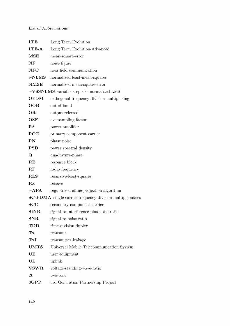
List of Abbreviations
LTE Long Term Evolution
LTE-A Long Term Evolution-Advanced
MSE mean-square-error
NF noise figure
NFC near field communication
ε-NLMS normalized least-mean-squares
NMSE normalized mean-square-error
ε-VSSNLMS variable step-size normalized LMS
OFDM orthogonal frequency-division multiplexing
OOB out-of-band
OR output-referred
OSF oversampling factor
PA power amplifier
PCC primary component carrier
PN phase noise
PSD power spectral density
Q quadrature-phase
RB resource block
RF radio frequency
RLS recursive-least-squares
Rx receive
ε-APA regularized affine-projection algorithm
SC-FDMA single-carrier frequency-division multiple access
SCC secondary component carrier
SINR signal-to-interference-plus-noise ratio
SNR signal-to-noise ratio
TDD time-division duplex
Tx transmit
TxL transmitter leakage
UMTS Universal Mobile Telecommunication System
UE user equipment
UL uplink
VSWR voltage-standing-wave-ratio
2t two-tone
3GPP 3rd Generation Partnership Project
142

Bibliography
[1] 3GPP, “3rd Generation Partnership Project; Technical Specification GroupRadio Access Network; Evolved Universal Terrestrial Radio Access (E-UTRA);User Equipment (UE) radio transmission and reception (Release 10),” 3GPP,Tech. Rep., May 2015. [Online]. Available: http://www.3gpp.org/ftp/Specs/latest prior-to-2018-03/Rel-10/36 series/36807-a00.zip
[2] A. A. Abidi, “Direct-conversion radio transceivers for digital communications,” InIEEE Journal of Solid-State Circuits, Vol. 30, No. 12, pp. 1399–1410, Dec 1995.
[3] 3GPP, “Evolved Universal Terrestrial Radio Access (E-UTRA); User Equipment(UE) radio transmission and reception,” 3GPP, Tech. Rep., May 2015. [Online].Available: http://www.3gpp.org/ftp/specs/archive/36 series/36.101/36101-bg0.zip
[4] Ericsson and ST-Ericsson, “R4-126964, REFSENS with one UL carrier forNC intra-band CA,” Ericsson, Tech. Rep., November 2012. [Online]. Available:http://www.3gpp.org/ftp/tsg ran/WG4 Radio/TSGR4 65/docs/R4-126964.zip
[5] R. Vazny, W. Schelmbauer, H. Pretl, S. Herzinger, and R. Weigel, “An interstagefilter-free mobile radio receiver with integrated TX leakage filtering,” In Proceedingsof the IEEE Radio Frequency Integrated Circuits Symposium, May 2010, pp. 21–24.
[6] A. Kiayani, L. Anttila, and M. Valkama, “Modeling and dynamic cancellation ofTX-RX leakage in FDD transceivers,” In Proceedings of the 56th InternationalMidwest Symposium on Circuits and Systems (MWSCAS), Aug 2013, pp. 1089–1094.
[7] A. Gebhard, C. Motz, R. S. Kanumalli, H. Pretl, and M. Huemer, “Nonlinear least-mean-squares type algorithm for second-order interference cancellation in LTE-ARF transceivers,” In Proceedings of the 51st Asilomar Conference on Signals, Sys-tems, and Computers, Oct 2017, pp. 802–807.
[8] B. Razavi, “Design considerations for direct-conversion receivers,” In IEEE Trans-actions on Circuits and Systems II: Analog and Digital Signal Processing, Vol. 44,No. 6, pp. 428–435, Jun 1997.
[9] A. Gebhard, R. S. Kanumalli, B. Neurauter, and M. Huemer, “Adaptive self-interference cancelation in LTE-A carrier aggregation FDD direct-conversion trans-ceivers,” In Proceedings of the 9th IEEE Sensor Array and Multichannel SignalProcessing Workshop (SAM 2016), July 2016, pp. 1–5.
[10] R. S. Kanumalli, A. Gebhard, A. Elmaghraby, A. Mayer, D. Schwartz, and M. Hue-mer, “Active Digital Cancellation of Transmitter Induced Modulated Spur Inter-ference in 4G LTE Carrier Aggregation Transceivers,” In Proceedings of the 83rdIEEE Vehicular Technology Conference (VTC Spring), May 2016, pp. 1–5.
[11] A. Kiayani, M. Abdelaziz, L. Anttila, V. Lehtinen, and M. Valkama, “Digital Miti-gation of Transmitter-Induced Receiver Desensitization in Carrier Aggregation FDD
143
Bibliography
Transceivers,” In IEEE Transactions on Microwave Theory and Techniques, Vol. 63,No. 11, pp. 3608–3623, Nov 2015.
[12] A. Kiayani, M. Z. Waheed, L. Anttila, M. Abdelaziz, D. Korpi, V. Syrjala, M. Ko-sunen, K. Stadius, J. Ryynanen, and M. Valkama, “Adaptive Nonlinear RF Cancel-lation for Improved Isolation in Simultaneous Transmit–Receive Systems,” In IEEETransactions on Microwave Theory and Techniques, Vol. 66, No. 5, pp. 2299–2312,May 2018.
[13] A. Elmaghraby, “Transmitter Leakage Cancellation in Cellular Handset Receivers,”Dissertation, University of Erlangen-Nuremberg, July 2016.
[14] H. Khatri, P. S. Gudem, and L. E. Larson, “An Active Transmitter Leakage Sup-pression Technique for CMOS SAW-Less CDMA Receivers,” In IEEE Journal ofSolid-State Circuits, Vol. 45, No. 8, pp. 1590–1601, Aug 2010.
[15] A. Elmaghraby, R. S. Kanumalli, W. Schelmbauer, A. Mayer, S. Herzinger,D. Schwartz, M. Huemer, and R. Weigel, “A Mixed-Signal Technique for TX-Induced Modulated Spur Cancellation in LTE-CA Receivers,” In IEEE Transac-tions on Circuits and Systems I: Regular Papers, Vol. 65, No. 9, pp. 3060–3073,Sep. 2018.
[16] S. Sadjina, R. S. Kanumalli, A. Gebhard, K. Dufrene, M. Huemer, and H. Pretl, “AMixed-Signal Circuit Technique for Cancellation of Interferers Modulated by LOPhase-Noise in 4G/5G CA Transceivers,” In IEEE Transactions on Circuits andSystems I: Regular Papers, Vol. 65, No. 11, pp. 3745–3755, Nov 2018.
[17] M. Faulkner, “DC offset and IM2 removal in direct conversion receivers,” In IEEProceedings - Communications, Vol. 149, No. 3, pp. 179–184, Jun 2002.
[18] M. Faulkner, “IM2 removal in direct conversion receivers,” In Proceedings of the53rd Vehicular Technology Conference, Vol. 3, May 2001, pp. 1897–1901.
[19] A. Kiayani, L. Anttila, M. Kosunen, K. Stadius, J. Ryynanen, and M. Valkama,“Modeling and Joint Mitigation of TX and RX Nonlinearity-Induced Receiver De-sensitization,” In IEEE Transactions on Microwave Theory and Techniques, Vol. 65,No. 7, pp. 2427–2442, July 2017.
[20] A. Kiayani, L. Anttila, and M. Valkama, “Digital Suppression of Power Ampli-fier Spurious Emissions at Receiver Band in FDD Transceivers,” In IEEE SignalProcessing Letters, Vol. 21, No. 1, pp. 69–73, Jan 2014.
[21] A. Frotzscher and G. Fettweis, “A Stochastic Gradient LMS Algorithm for DigitalCompensation of Tx Leakage in Zero-IF-Receivers,” In Proceedings of the VehicularTechnology Conference (VTC Spring 2008), May 2008, pp. 1067–1071.
[22] C. Lederer and M. Huemer, “LMS Based Digital Cancellation of Second-Order TXIntermodulation Products in Homodyne Receivers,” In Proceedings of the Radioand Wireless Symposium (RWS), Jan 2011, pp. 207–210.
144
Bibliography
[23] A. Frotzscher and G. Fettweis, “Least Squares Estimation for the Digital Compen-sation of Tx Leakage in zero-IF Receivers,” In Proceedings of the Global Telecom-munications Conference (GLOBECOM 2009), Nov 2009, pp. 1–6.
[24] D. H. Brandwood, “A complex gradient operator and its application in adaptive ar-ray theory,” In IEE Proceedings F - Communications, Radar and Signal Processing,Vol. 130, No. 1, pp. 11–16, February 1983.
[25] V. J. Mathews and G. L. Sicuranza, Polynomial signal processing. Wiley-Interscience, 2000.
[26] T. Ogunfunmi, Adaptive nonlinear system identification: the Volterra and Wienermodel approaches. Springer Science & Business Media, 2007.
[27] A. Gebhard, O. Lang, M. Lunglmayr, C. Motz, R. S. Kanumalli, C. Auer,T. Paireder, M. Wagner, H. Pretl, and M. Huemer, “A Robust Nonlinear RLS TypeAdaptive Filter for Second-Order-Intermodulation Distortion Cancellation in FDDLTE and 5G Direct Conversion Transceivers,” In IEEE Transactions on MicrowaveTheory and Techniques, 16 pages, Early Access, January 2019.
[28] TDK, “SAW Duplexer B8576,” TDK, Tech. Rep., February 2015. [Online].Available: https://en.rf360jv.com/inf/40/ds/mc/B8576.pdf
[29] A. Mirzaei, H. Darabi, J. Leete, and Y. Chang, “Analysis and Optimization ofDirect-Conversion Receivers With 25% Duty-Cycle Current-Driven Passive Mixers,”In Circuits and Systems I: Regular Papers, IEEE Transactions on, Vol. 57, No. 9,pp. 2353–2366, Sept 2010.
[30] A. Kiayani, V. Lehtinen, L. Anttila, T. Lahteensuo, and M. Valkama, “LinearityChallenges of LTE-Advanced Mobile Transmitters: Requirements and PotentialSolutions,” In IEEE Communications Magazine, Vol. 55, No. 6, pp. 170–179, 2017.
[31] M. Mikhemar, D. Murphy, A. Mirzaei, and H. Darabi, “A Cancellation Techniquefor Reciprocal-Mixing Caused by Phase Noise and Spurs,” In IEEE Journal ofSolid-State Circuits, Vol. 48, No. 12, pp. 3080–3089, Dec 2013.
[32] H. T. Dabag, H. Gheidi, P. Gudem, and P. M. Asbeck, “All-digital cancellationtechnique to mitigate self-jamming in uplink carrier aggregation in cellular hand-sets,” In 2013 IEEE MTT-S International Microwave Symposium Digest (MTT),June 2013, pp. 1–3.
[33] W. Rhee and K. Iniewski, Wireless Transceiver Circuits. CRC Press, 2015.
[34] R. Tzschoppe and J. B. Huber, “Causal discrete-time system approximation of non-bandlimited continuous-time systems by means of discrete prolate spheroidal wavefunctions,” In European Transactions on Telecommunications, Vol. 20, No. 6, pp.604–616, Aug 2008.
[35] A. V. Oppenheim, R. W. Schafer, and J. R. Buck, Discrete-time signal processing.Prentice Hall, 1999.
145
Bibliography
[36] M. Valkama, M. Renfors, and V. Koivunen, “Advanced Methods for I/Q Imbal-ance Compensation in Communication Receivers,” In IEEE Transactions on SignalProcessing, Vol. 49, No. 10, pp. 2335–2344, Oct 2001.
[37] M. Valkama, A. Springer, and G. Hueber, “Digital signal processing for reducing theeffects of RF imperfections in radio devices - An overview,” In Proceedings of theIEEE International Symposium on Circuits and Systems, May 2010, pp. 813–816.
[38] H. Darabi, Radio Frequency Integrated Circuits and Systems. Cambridge UniversityPress, 2015.
[39] A. Walid, “Effective IM2 products estimation for two-tone and W-CDMA modu-lated blockers in 3GPP direct-conversion receivers,” Maxim Integrated, Tech. Rep.,2004.
[40] J. Hector, C. Sturm, and J. Ponte, Radio Systems Engineering: A Tutorial Ap-proach. Springer, 2014.
[41] I. Reed, “On a moment theorem for complex Gaussian processes,” In IRE Trans-actions on Information Theory, Vol. 8, No. 3, pp. 194–195, April 1962.
[42] M. Ahsanullah, B. G. Kibria, and M. Shakil, Normal and student’s t distributionsand their applications. Springer, 2014.
[43] D. Stuetzle, “Understanding IP2 and IP3 Issues in Direct Conversion Receivers forWCDMA Wide Area Basestations,” In High Frequency Electronics, Vol. 7, No. 6,2008.
[44] E. S. Atalla, A. Bellaouar, and P. T. Balsara, “IIP2 requirements in 4G LTE handsetreceivers,” In Proceedings of the 56th International Midwest Symposium on Circuitsand Systems (MWSCAS), Aug 2013, pp. 1132–1135.
[45] C. W. Liu and M. Damgaard, “IP2 and IP3 nonlinearity specifications for3G/WCDMA receivers,” In High Frequency Electronics, pp. 16–29, 2009.
[46] I. Madadi, M. Tohidian, K. Cornelissens, P. Vandenameele, and R. B. Staszewski,“A High IIP2 SAW-Less Superheterodyne Receiver With Multistage Harmonic Re-jection,” In IEEE Journal of Solid-State Circuits, Vol. 51, No. 2, pp. 332–347, Feb2016.
[47] K. Dufrene, Z. Boos, and R. Weigel, “Digital Adaptive IIP2 Calibration Scheme forCMOS Downconversion Mixers,” In IEEE Journal of Solid-State Circuits, Vol. 43,No. 11, pp. 2434–2445, Nov 2008.
[48] A. Mirzaei, H. Darabi, J. C. Leete, X. Chen, K. Juan, and A. Yazdi, “Analysis andOptimization of Current-Driven Passive Mixers in Narrowband Direct-ConversionReceivers,” In IEEE Journal of Solid-State Circuits, Vol. 44, No. 10, pp. 2678–2688,Oct 2009.
[49] J. Weldon, R. Narayanaswami, J. Rudell, L. Lin, M. Otsuka, S. Dedieu, L. Tee,K.-C. Tsai, C.-W. Lee, and P. Gray, “A 1.75-GHz highly integrated narrow-bandCMOS transmitter with harmonic-rejection mixers,” In IEEE Journal of Solid-StateCircuits, Vol. 36, No. 12, pp. 2003–2015, Dec 2001.
146
Bibliography
[50] T. Forbes, W.-G. Ho, and R. Gharpurey, “Design and Analysis of Harmonic Rejec-tion Mixers With Programmable LO Frequency,” In IEEE Journal of Solid-StateCircuits, Vol. 48, No. 10, pp. 2363–2374, Oct 2013.
[51] H. Zhang, T. B. Gao, S. Tan, and O. Shana’A, “A harmonic-rejection mixer withimproved design algorithm for broadband TV tuners,” In Proceedings of the IEEERadio Frequency Integrated Circuits Symposium (RFIC), June 2012, pp. 163–166.
[52] Y. H. Chen, N. Fong, B. Xu, and C. Wang, “An LTE SAW-less transmitter using33% duty-cycle LO signals for harmonic suppression,” In 2015 IEEE InternationalSolid-State Circuits Conference - (ISSCC) Digest of Technical Papers, Feb 2015,pp. 1–3.
[53] R. Bagheri, A. Mirzaei, S. Chehrazi, M. E. Heidari, M. Lee, M. Mikhemar, W. Tang,and A. A. Abidi, “An 800-MHz ndash;6-GHz Software-Defined Wireless Receiverin 90-nm CMOS,” In IEEE Journal of Solid-State Circuits, Vol. 41, No. 12, pp.2860–2876, Dec 2006.
[54] F. Gatta, R. Gomez, Y. Shin, T. Hayashi, H. Zou, J. Y. C. Chang, L. Dauphinee,J. Xiao, D. S. H. Chang, T. H. Chih, M. Brandolini, D. Koh, B. J. J. Hung, T. Wu,M. Introini, G. Cusmai, L. Tan, B. Currivan, L. He, P. Cangiane, and P. Vorenkamp,“An embedded 65nm CMOS low-IF 48MHz-to-1GHz dual tuner for DOCSIS 3.0,”In 2009 IEEE International Solid-State Circuits Conference - Digest of TechnicalPapers, Feb 2009, pp. 122–123,123a.
[55] K. Kibaroglu and G. M. Rebeiz, “A 0.05 -6 GHz voltage-mode harmonic rejectionmixer with up to 30 dBm in-band IIP3 and 35 dBc HRR in 32 nm SOI CMOS,”In 2017 IEEE Radio Frequency Integrated Circuits Symposium (RFIC), June 2017,pp. 304–307.
[56] D. Murphy, H. Darabi, and H. Xu, “A Noise-Cancelling Receiver Resilient to LargeHarmonic Blockers,” In IEEE Journal of Solid-State Circuits, Vol. 50, No. 6, pp.1336–1350, June 2015.
[57] A. Gebhard, S. Sadjina, K. Dufrene, and S. Tertinek, “Harmonic Suppressing LocalOscillator Signal Generation,” US Patent 9,935,722 B2, granted March 2018.
[58] D. P. Mandic and V. S. L. Goh, Complex valued nonlinear adaptive filters: noncir-cularity, widely linear and neural models. John Wiley & Sons, 2009, Vol. 59.
[59] P. S. Diniz, Adaptive Filtering, Algorithms and Practical Implementation. Springer,2013.
[60] H. G. Myung, “Introduction to single carrier FDMA,” In Proceedings of the 15thEuropean Signal Processing Conference (EUSIPCO), Sept 2007, pp. 2144–2148.
[61] A. H. Sayed, Fundamentals of adaptive filtering. John Wiley & Sons, 2003.
[62] P. Schreier and L. L. Scharf, Statistical Signal Processing of Complex-Valued Data:The Theory of Improper and Noncircular Signals. Cambridge University Press,2010.
147
Bibliography
[63] R. Hunger, “An introduction to complex differentials and complex differentiability,”Technische Universitat Munchen. TUM-LNS-TR-07-06, October 2007., Tech. Rep.,2007.
[64] R. F. H. Fischer, Appendix A: Wirtinger Calculus. Wiley-Blackwell, 2005,pp. 405–413. [Online]. Available: https://onlinelibrary.wiley.com/doi/abs/10.1002/0471439002.app1
[65] A. van den Bos, “Complex gradient and Hessian,” In IEE Proceedings - Vision,Image and Signal Processing, Vol. 141, No. 6, pp. 380–383, Dec 1994.
[66] A. I. Hanna and D. P. Mandic, “A fully adaptive normalized nonlinear gradientdescent algorithm for complex-valued nonlinear adaptive filters,” In IEEE Trans-actions on Signal Processing, Vol. 51, No. 10, pp. 2540–2549, Oct 2003.
[67] K. Kreutz-Delgado, “The Complex Gradient Operator and the CR-Calculus,”Electrical and Computer Engineering, Jacobs School of Engineering, Universityof California, San Diego, Tech. Rep., 2009. [Online]. Available: https://arxiv.org/pdf/0906.4835.pdf
[68] M. A. Woodbury, “Inverting Modified Matrices,” Statistical Research Group Mem-orandum Reports. Princeton, NJ: Princeton University, 1950, No. 42., Tech. Rep.,1950.
[69] E. C. Levy, “Complex-curve fitting,” In IRE Transactions on Automatic Control,Vol. AC-4, No. 1, pp. 37–43, May 1959.
[70] J. Zyren and W. McCoy, “Overview of the 3GPP long term evolution physical layer,”Freescale Semiconductor, Inc., Tech. Rep., 2007. [Online]. Available: https://www.nxp.com/files/wireless comm/doc/white paper/3GPPEVOLUTIONWP.pdf
[71] M. Kahrizi, J. Komaili, J. E. Vasa, and D. Agahi, “Adaptive filtering using LMSfor digital TX IM2 cancellation in WCDMA receiver,” In Proceedings of the IEEERadio and Wireless Symposium, Jan 2008, pp. 519–522.
[72] H. Gheidi, H. T. Dabag, Y. Liu, P. M. Asbeck, and P. Gudem, “Digital cancella-tion technique to mitigate receiver desensitization in cellular handsets operating incarrier aggregation mode with multiple uplinks and multiple downlinks,” In Pro-ceedings of the IEEE Radio and Wireless Symposium (RWS), Jan 2015, pp. 221–224.
[73] C. Lederer and M. Huemer, “Simplified complex LMS algorithm for the cancel-lation of second-order TX intermodulation distortions in homodyne receivers,” InProceedings of the Forty Fifth Asilomar Conference on Signals, Systems and Com-puters (ACSSC), Nov 2011, pp. 533–537.
[74] R. Isermann, Identifikation dynamischer Systeme 1. Springer-Verlag, 1991.
[75] M. Rupp and R. Frenzel, “Analysis of LMS and NLMS algorithms with delayedcoefficient update under the presence of spherically invariant processes,” In IEEETransactions on Signal Processing, Vol. 42, No. 3, pp. 668–672, March 1994.
148
Bibliography
[76] A. Gebhard, “Second Order Intermodulation Cancellation for RF Transceivers,” USPatent 2018/015 417, filed June 2017.
[77] Y. Chen, T. Le-Ngoc, B. Champagne, and C. Xu, “Recursive least squares con-stant modulus algorithm for blind adaptive array,” In IEEE Transactions on SignalProcessing, Vol. 52, No. 5, pp. 1452–1456, May 2004.
[78] Y. X. Chen, Z. Y. He, T. S. Ng, and P. C. K. Kwok, “RLS adaptive blind beamform-ing algorithm for cyclostationary signals,” In Electronics Letters, Vol. 35, No. 14,pp. 1136–1138, July 1999.
[79] R. Ferrus and O. Sallent, Mobile Broadband Communications for Public Safety: TheRoad Ahead Through LTE Technology. Wiley, 2015.
[80] S. Gunnarsson, “Combining tracking and regularization in recursive least squaresidentification,” In Proceedings of 35th IEEE Conference on Decision and Control,Dec 1996, pp. 2551–2552.
[81] T. Huckle and M. Sedlacek, “Data Based Regularization Matrices for the Tikhonov-Phillips Regularization,” In Proceedings of the Applied Mathematics and Mechanics(PAMM). Wiley Online Library, 2012, pp. 643–644.
[82] J. Dokoupil and V. Burlak, “Variable Regularized Square Root Recursive LeastSquare Method,” In Proceedings of the 11th IFAC IEEE International Conferenceon Programmable Devices and Embedded Systems, 2012, pp. 78–82.
149


Curriculum Vitae
Personal Information
Andreas GebhardParkstraße 8/94230 Pregarten, Austria+43 (0)680 [email protected]
Education
2014 – 2018 PhD in Technical Sciences, Johannes Kepler University Linz
PhD thesis: ”Self-Interference Cancellation and Rejection inFDD RF-Transceivers” conducted at the Institute of SignalProcessing (ISP), and in cooperation with DMCE/Intel Austria.
2009 – 2011 MSc (Dipl.-Ing.) in Electrical Engineering, Graz Universityof Technology, with distinction
Major in Control and Automation. Master thesis: Construction and Control of the Laboratory
Model ”Car on a Rotatable Beam” conducted at the Institutefor Control and Automation (IRT).
2006 – 2009 BSc in Electrical Engineering, Graz University of Technology
Bachelor Thesis: ”Modeling, Control and Simulation of SwitchedMode Power Supplies” conducted at the Institute for Controland Automation (IRT).
1996 – 2001 Technical College (Telecommunications), HTL Rankweil
Degree project: ”Class-D Switched Mode Audio PowerAmplifier”.
151

Curriculum Vitae
Experience
Since12/2014
PhD in Technical Sciences, Johannes Kepler University Linzin cooperation with DMCE/Intel, Linz, full time
Mentor of three PhD students Co-supervisor of one master thesis Reviewer for several journal and conference papers Various PR activities in form of talks, seminars, and exhibitions
03/2013 –11/2014
Development of Mechatronic Systems, Linz Center ofMechatronics, Linz, full time
Condition monitoring concepts for gas valves and injectionmolding machines
Control design for an electronic shaft of a manned transportsystem
Acoustic localization of miners around the digging machineusing time-of-flight measurements
04/2012 –02/2013
Implementation of Control Algorithms in PLC ControlUnits, Schelling Anlagenbau, Schwarzach, full time
Control of fully automated and time optimized wood and steelsaws
Implementation of digital filters Commissioning of saws in Germany and Spain
11/2011 –02/2012
Trip to New Zealand and Australia
08/2010 –09/2010
Internship, ATB Motors, Lustenau, full time
Control of a brush-less DC motor with back-EMF detection
07/2008 –08/2008
Internship, Tridonic.ATCO, Dornbirn, full time
Patent-department: Analysis of competitive products for patentviolations
05/2002 –07/2006
Design of electronic control gears for fluorescent lamps,Tridonic.ATCO, Dornbirn, full time
Dimensioning of the electrical components (L,C) required for theresonance circuitry
Testing of the electronic gears for standardization requirements(ENEC, EN, ISO)
Accompaniment of the products till the null-series and seriesmaturity
152
07/1999 –08/1999
Internship, Siemens, Bregenz, full time
Testing of fireboxes Construction of electric cabinets
07/1998 –08/1998
Internship, Fawai & Co, Bregenz, full time
Repairing of televisions and radios Commissioning televisions at customers
Language Skills
German (mother tongue) English
Patents / Patent Applications
A. Gebhard, S. Sadjina, K. Dufrene and S. Tertinek, ”Harmonic Suppressing Lo-cal Oscillator Signal Generation,” U.S. Patent US 9,935,722 B2, filed June 2016,granted April 2018.
S. Tertinek, A. Gebhard, S. Sadjina and K. Dufrene, ”Pulse Generation UsingDigital-to-Time Converter,” U.S. Patent US 9,755,872 B1, filed August 2016,granted September 2017.
K. Dufrene, Ram S. Kanumalli, S. Sadjina and A. Gebhard, ”Multiple ModulatedSpur Cancellation Apparatus,” U.S. Patent Application US 2017/0359136 A1, filedJune 2016, published December 2017.
A. Gebhard, ”Second Order Intermodulation Cancellation for RF Transceivers,”U.S. Patent US 10,172,143 B2, filed June 2017, granted January 2019.
K. Dufrene, S. Sadjina, A. Gebhard and Ram S. Kanumalli, ”Interference De-tection Device, Interference Detection Apparatus, Interference Detection Method,Computer Program, Receiver, Mobile Terminal and Base Station,” U.S. Patent US10,097,220 B2, filed May 2017, granted October 2018.
153
Curriculum Vitae
Journal Publications
A. Gebhard, O. Lang, M. Lunglmayr, C. Motz, R. S. Kanumalli, C. Auer, T.Paireder, M. Wagner, H. Pretl and M. Huemer, ”A Robust Nonlinear RLS TypeAdaptive Filter for Second-Order-Intermodulation Distortion Cancellation in FDDLTE and 5G Direct Conversion Transceivers,” In IEEE Transactions on MicrowaveTheory and Techniques, 16 pages, Early Access, January 2019.
S. Sadjina, R. S. Kanumalli, A. Gebhard, K. Dufrene, M. Huemer and H. Pretl,”A Mixed-Signal Circuit Technique for Cancellation of Interferers Modulated byLO Phase-Noise in 4G/5G CA Transceivers,” In IEEE Transactions on Circuitsand Systems – I Regular Papers, Vol. 65, No. 11, pp. 3745-3755, Nov 2018.
R. S. Kanumalli, T. Buckel, C. Preissl, P. Preyler, A. Gebhard, C. Motz, J.Markovic, D. Hamidovic, E. Hager, H. Pretl, A. Springer and M. Huemer, ”Digitally-intensive Transceivers for Future Mobile Communications - Emerging Trends andChallenges,” In e&i Elektrotechnik und Informationstechnik, Vol. 135, No. 1, pp.30-39, January 2018.
Conference Publications
A. Gebhard and C. Motz and R. S. Kanumalli and H. Pretl and M. Huemer, ”Non-linear Least-Mean-Squares Type Algorithm for Second-Order Interference Can-cellation in LTE-A RF Transceivers,” In Proceedings of the 51st IEEE AsilomarConference on Signals, Systems, and Computers (ACSSC), Oct 2017, pp. 802-807.
A. Gebhard, M. Lunglmayr and M. Huemer, ”Investigations on Sparse SystemIdentification with l0-LMS, Zero-Attracting LMS and Linearized Bregman Itera-tions,” In Proceedings of the 16th International Conference on Computer AidedSystem Theory - EUROCAST, February 2018.
A. Gebhard and R. S. Kanumalli and B. Neurauter and M. Huemer, ”Adaptive Self-Interference Cancellation in LTE-A Carrier Aggregation FDD Direct-ConversionTransceivers,” In Proceedings of the IEEE Sensor Array and Multichannel SignalProcessing Workshop (SAM 2016), July 2016, pp. 1-5.
R. S. Kanumalli, A. Gebhard, A. Elmaghraby, A. Mayer, D. Schwartz and M.Huemer, ”Active Digital Cancellation of Transmitter Induced Modulated SpurInterference in 4G LTE Carrier Aggregation Transceivers,” In Proceedings of the83rd IEEE Vehicular Technology Conference (VTC Spring), May 2016, pp. 1-5.
154
Related Documents