IEEE TRANSACTIONS ON ADVANCED PACKAGING, VOL. 33,NO. 4,NOVEMBER 2010 979 Self-Consistent Simulation of Opto-Electronic Circuits Using a Modified Nodal Analysis Formulation Pavan Gunupudi, Member, IEEE, Tom Smy, Jackson Klein, and Z. Jan Jakubczyk Abstract—This paper addresses the need for self-consistent simulation of mixed electrical and optical circuits and systems. Drawing on the use of modified nodal analysis (MNA) techniques ubiquitous in circuit simulation, an optical node is formulated which includes the magnitude and phase of the optical signal being simulated. This node consists of two propagating complex envelopes one for the forward direction and the other for the re- verse direction. Using this formulation models are developed for a variety of devices including: lasers, photodiodes, multimode fiber, and optical connectors. The formulation allows for definition of multiple optical channels at different carrier frequencies, enables quick simulation of systems with large optical delays and optical interference effects. Several numerical examples are presented in this paper to illustrate the capability of the proposed framework and where practicable the results were compared to commercial simulators. These examples include a multimode fiber optical link, an integrated array of laser sources and a feedback controlled laser source used in a optical link with modulation achieved by the use of an electro-absorption device. Index Terms—Circuit simulation, electrothermal effects, in- tegrated optoelectronics, laser thermal factors, multi-physics simulation, optical communication, optoelectronic devices, opto- electronic feedback, photothermal effects. I. INTRODUCTION T HE recent past has seen a rapid growth of complexity and capability in the field of electronics. In particular operating frequencies of devices have continued to increase leading to the presence of high-frequency effects. These signal-degrading effects along with large pin-out densities at packages motivated research in alternate interconnection tech- niques using optical interconnects and devices within chips and printed circuit boards (PCBs) [1]–[5]. The presence of optical interconnects at the microelectronic level also necessitates the presence of optical drivers, receivers, modulators, and other optical components along with their electrical counterparts at this level of design hierarchy. This co-existence of electrical and optical components in the microelectronic realm is gradu- ally ushering in an era which will require a very high level of integration between electrical and optical components. Manuscript received November 09, 2009; revised May 05, 2010; accepted June 01, 2010. Date of publication July 29, 2010; date of current version January 07, 2011. This work was recommended for publication by Associate Editor A. Maffucci upon evaluation of the reviewers comments. P. Gunupudi and T. Smy are with Department of Electronics, Carleton Uni- versity, Ottawa, K1S 5B6 ON, Canada. J. Klein and Z. J. Jakubczyk are with Optiwave Systems Inc., Ottawa, K1S 5B6, Canada. Digital Object Identifier 10.1109/TADVP.2010.2054089 The drive for higher level integration initially manifested as board and package level integration using hybrid technologies such as system on a package (SOP), and a variety of novel substrate technologies [6]–[9]. More recently, integrated pho- tonic solutions based on Silicon substrates have been investi- gated. Silicon has a number of natural advantages, chief among them the extremely mature fabrication technology, low cost, and very well developed electrical design environment [10]–[12]. Using a mixture of traditional technology, nano-scale fabrica- tion and organic materials, a wide variety of devices have been proposed for the development of integrated opto-electronic cir- cuits [2]–[5]. The continued development of SOP and silicon photonics will likely lead to the rapid integration of photonic elements and electrical devices at the chip, board, and system level in an effort to lower costs and create new opportunities [13], [14]. A significant advantage of optical systems over electrical systems is the ability to carry information signals in separate channels within the same optical waveguide—be it an optical fiber or a ridge waveguide in an integrated optical solution. Each channel is operated at a different optical carrier wave- length. Such a system is referred to as a wavelength division multiplexing (WDM) system [15]. Essentially, the very large bandwidth of an optical interconnect is divided into a number of regions of smaller bandwidth each characterized by a carrier frequency (also known as center frequency). A variety of WDM configurations are used including dense/coarse WDM using single mode fiber [15], typically for long distances, and single channel or coarse WDM with multimode fiber for more local interconnects [16]. The combination of tight optical-electrical integration, thermal coupling and the need to model optical effects such as interference, reflection and multiple carrier frequencies presents a significant design challenge that needs to be ad- dressed. Design of optoelectronic circuits having a high level of integration between both energy domains requires simulation tools capable of accurately and efficiently handling signal flow across optical and electrical components while capturing mutual interactions between these different energy domains. Several attempts [17]–[21] to simulate optical and electrical components together are present in the literature. Chatoyant is an optoelectronic simulation methodology modeled around a hierarchically heterogeneous system-level simulation frame- work called Ptolemy [22]–[24]. Chatoyant handles nonlinear elements in the system by representing them using piecewise linear models and forms a linear network for the optoelectronic 1521-3323/$26.00 © 2010 IEEE

Welcome message from author
This document is posted to help you gain knowledge. Please leave a comment to let me know what you think about it! Share it to your friends and learn new things together.
Transcript
IEEE TRANSACTIONS ON ADVANCED PACKAGING, VOL. 33, NO. 4, NOVEMBER 2010 979
Self-Consistent Simulation of Opto-ElectronicCircuits Using a Modified Nodal Analysis
FormulationPavan Gunupudi, Member, IEEE, Tom Smy, Jackson Klein, and Z. Jan Jakubczyk
Abstract—This paper addresses the need for self-consistentsimulation of mixed electrical and optical circuits and systems.Drawing on the use of modified nodal analysis (MNA) techniquesubiquitous in circuit simulation, an optical node is formulatedwhich includes the magnitude and phase of the optical signalbeing simulated. This node consists of two propagating complexenvelopes one for the forward direction and the other for the re-verse direction. Using this formulation models are developed for avariety of devices including: lasers, photodiodes, multimode fiber,and optical connectors. The formulation allows for definition ofmultiple optical channels at different carrier frequencies, enablesquick simulation of systems with large optical delays and opticalinterference effects. Several numerical examples are presented inthis paper to illustrate the capability of the proposed frameworkand where practicable the results were compared to commercialsimulators. These examples include a multimode fiber optical link,an integrated array of laser sources and a feedback controlledlaser source used in a optical link with modulation achieved by theuse of an electro-absorption device.
Index Terms—Circuit simulation, electrothermal effects, in-tegrated optoelectronics, laser thermal factors, multi-physicssimulation, optical communication, optoelectronic devices, opto-electronic feedback, photothermal effects.
I. INTRODUCTION
T HE recent past has seen a rapid growth of complexityand capability in the field of electronics. In particular
operating frequencies of devices have continued to increaseleading to the presence of high-frequency effects. Thesesignal-degrading effects along with large pin-out densities atpackages motivated research in alternate interconnection tech-niques using optical interconnects and devices within chips andprinted circuit boards (PCBs) [1]–[5]. The presence of opticalinterconnects at the microelectronic level also necessitates thepresence of optical drivers, receivers, modulators, and otheroptical components along with their electrical counterparts atthis level of design hierarchy. This co-existence of electricaland optical components in the microelectronic realm is gradu-ally ushering in an era which will require a very high level ofintegration between electrical and optical components.
Manuscript received November 09, 2009; revised May 05, 2010; acceptedJune 01, 2010. Date of publication July 29, 2010; date of current version January07, 2011. This work was recommended for publication by Associate Editor A.Maffucci upon evaluation of the reviewers comments.
P. Gunupudi and T. Smy are with Department of Electronics, Carleton Uni-versity, Ottawa, K1S 5B6 ON, Canada.
J. Klein and Z. J. Jakubczyk are with Optiwave Systems Inc., Ottawa, K1S5B6, Canada.
Digital Object Identifier 10.1109/TADVP.2010.2054089
The drive for higher level integration initially manifested asboard and package level integration using hybrid technologiessuch as system on a package (SOP), and a variety of novelsubstrate technologies [6]–[9]. More recently, integrated pho-tonic solutions based on Silicon substrates have been investi-gated. Silicon has a number of natural advantages, chief amongthem the extremely mature fabrication technology, low cost, andvery well developed electrical design environment [10]–[12].Using a mixture of traditional technology, nano-scale fabrica-tion and organic materials, a wide variety of devices have beenproposed for the development of integrated opto-electronic cir-cuits [2]–[5]. The continued development of SOP and siliconphotonics will likely lead to the rapid integration of photonicelements and electrical devices at the chip, board, and systemlevel in an effort to lower costs and create new opportunities[13], [14].
A significant advantage of optical systems over electricalsystems is the ability to carry information signals in separatechannels within the same optical waveguide—be it an opticalfiber or a ridge waveguide in an integrated optical solution.Each channel is operated at a different optical carrier wave-length. Such a system is referred to as a wavelength divisionmultiplexing (WDM) system [15]. Essentially, the very largebandwidth of an optical interconnect is divided into a numberof regions of smaller bandwidth each characterized by a carrierfrequency (also known as center frequency). A variety of WDMconfigurations are used including dense/coarse WDM usingsingle mode fiber [15], typically for long distances, and singlechannel or coarse WDM with multimode fiber for more localinterconnects [16].
The combination of tight optical-electrical integration,thermal coupling and the need to model optical effects suchas interference, reflection and multiple carrier frequenciespresents a significant design challenge that needs to be ad-dressed. Design of optoelectronic circuits having a high level ofintegration between both energy domains requires simulationtools capable of accurately and efficiently handling signalflow across optical and electrical components while capturingmutual interactions between these different energy domains.Several attempts [17]–[21] to simulate optical and electricalcomponents together are present in the literature. Chatoyant isan optoelectronic simulation methodology modeled around ahierarchically heterogeneous system-level simulation frame-work called Ptolemy [22]–[24]. Chatoyant handles nonlinearelements in the system by representing them using piecewiselinear models and forms a linear network for the optoelectronic
1521-3323/$26.00 © 2010 IEEE
980 IEEE TRANSACTIONS ON ADVANCED PACKAGING, VOL. 33, NO. 4, NOVEMBER 2010
system which is then simulated in the frequency domain.iSmile and iFrost perform optoelectronic simulation using amixed-mode methodology by representing some componentsin the time domain and other components in the frequencydomain. The above-mentioned methods do not pay particularattention to the phase of the optical signal. Without accountingfor the phase of the optical signal, optical interference, phasephenomena, and chirp can not be simulated. These effects areessential in determining the performance of modern communi-cation systems.
This paper presents the theory and implementation of a newtime-domain optoelectronic circuit/system simulator called Op-tiSPICE. In discussing this simulation framework, this paperproposes a definition of an optical node and presents a method-ology to model optical signals for ensuring reliable and self-con-sistent co-simulation of optical and electrical signals in a singleengine. The proposed model for optical signals allows a SPICE-like approach to handle optical components in conjunction withelectrical elements. This simulator will be useful for mixed op-toelectronic systems currently used in telecommunications, in-formation processing, and sensors. In particular, integrated op-tical circuits/systems with close coupling of electrical/opticaland thermal phenomena is seen as a primary application.
Within this framework optical signals are characterized by acarrier wavelength (referred to as optical channels) and sets ofoptical modes. For example an optical element such as a multi-mode fiber may have two channels, one at 1300 nm and a secondat 1325 nm. Each channel will be represented by a set of modeshapes—these mode shapes may be numerically or analyticallydetermined. For each individual optical mode, two propagatingsignals are modelled using four state variables. These variablesrepresent magnitude and phase of the complex envelope of elec-tric field of forward and backward propagating light. This choiceof state variables proved to be suitable for inclusion of opto-electronic device models in a SPICE based electrical simulationframework [25]. A detailed discussion on the choice of thesestate variables will be presented in this paper.
A wide variety of optical and electrical elements were mod-eled using this framework and several examples were simulated.Circuits consting of linear lumped elements, BJTs, MOSFETS,S-Parameter elements (using recursive convolution), and dis-tributed elements were simulated in conjunction with severaloptical elements such as fibers, lasers, Mach-Zehnders, mod-ulators, and photodiodes. The simulation framework was suc-cessful in capturing complex optical effects such as dispersion,scattering, and interference. In addition, support for the thermaldependence of optical and electrical devices was added and ex-amples integrating optical, electrical, and thermal disciplineswere successfully simulated.
The following sections will present details on the basic sim-ulation approach, the implementation of the optical signal in-frastructure, and descriptions of characteristic devices. Finally,the capabilities of the simulator will be demonstrated using awide variety of examples, including an optical link consistingof a laser, multimode fiber and detector, an optical circulator, awavelength division multiplexing circuit, and a control circuitwhich stabilizes the output power of a laser with respect to tem-perature variations.
II. OPTICAL SIGNAL INFRASTRUCTURE
Electrical simulation engines such as SPICE [25] solve elec-trical circuits by converting equations governing electrical de-vices into a set of nonlinear algebraic differential equations andrepresenting them in a matrix form through a modified nodalanalysis (MNA) type of formulation [26]. MNA equations aretypically formed at each electrical node using Kirchhoff’s cur-rent law (KCL). This type of a formulation is possible becausethe and fields are conservative in the electrical domain.Matrices and nonlinear functions are then determined for a par-ticular device relating port voltages and currents. These relation-ships are referred to as an element “stamp.” Global matrices areformed by “stamping” each element. For an electrical circuit thestate variables in the MNA formulation are typically node volt-ages, currents and device charges.
The global matrices are then simulated in the time domainby using an integration technique such as Backward Euler,Trapezoidal Method or Gear’s Method [25]. At each time point,Newton Raphson iterations are used to solve the set of non-linear difference equations formed by the chosen integrationmethod to arrive at a valid solution. Nonuniform time steppingalgorithms are used to simulate the circuit efficiently whilepreserving accuracy. Alternatively, after a dc solution is found,the system equations can be linearized and a small-signalanalysis can be performed.
To incorporate optical signals into this framework, an appro-priate choice of representation of the electrical and magneticfield of light must be made. However, it has to be noted that theelectrical and magnetic fields in optical devices are nonconser-vative unlike their electrical counterparts. As such these fieldscannot be represented by variables such as voltages and cur-rents. The following subsections explore the issues related torepresenting optical signals in a SPICE framework and presenta viable choice of state variables to represent the electric andmagnetic field within an MNA-approach.
A. Modulated EM Waves
An optical circuit is formed of a network of elements, most ofwhich can be described as guided-wave devices. Such devicesconstrain the optical energy to flow either forwards or back-wards along the waveguide. Examples are lasers, ridge wave-guides, optical fibers, filters, and modulators. Within such a net-work, optical signals are propagated from device to device. Thesolution of Maxwell’s equations provides the physical nature ofthese signals. Solving these equations for a waveguide showsthat the optical energy will propagate in modes of the form[27], [28]
where is the normalized mode shape determined by thecross-sectional geometry of the waveguide, andare the time varying envelopes of the forward and backwardtravelling signals respectively, with and the cor-responding time varying phases, the carrier frequency, theeffective optical index of refraction for the mode, and the wave

GUNUPUDI et al.: SELF-CONSISTENT SIMULATION OF OPTO-ELECTRONIC CIRCUITS USING A MODIFIED NODAL ANALYSIS FORMULATION 981
Fig. 1. Single optical link for a signal between two optical nodes.
number. An optical signal therefore consists of an electro-mag-netic wave oscillating at a carrier frequency propagating along awaveguide modulated by an envelope of lower frequency. Spec-ifying a position of interest and integrating over and , thissignal can be represented as
where is the total electric field of light at a particularpoint in the optical device. The fixed phase shift of foreach wave can be absorbed into the terms and the signalcan be presented as
the sum of two counter propagating waves each with a complexmodulated envelope.
This formulation which includes the carrier frequency in thesignal (typically in the Terahertz range) gives rise to extremelysmall time steps during simulation. It is therefore desirable thatthe carrier frequency be removed when representing the signaland the envelope used. As the forward and backward travel-ling waves represented by these envelopes are independent (fora linear element), the total optical signal can be modelled astwo signals each uni-directional in nature. However, informa-tion related to the phase of the envelope needs to be retained asit is instrumental in modeling complex optical effects such asinterference and diffraction. In view of the above, it is sufficientto represent the forward signal by and the reversesignal by .
An optical signal can therefore be characterized by four statevariables describing its complex envelope; the magnitude andphase of the forward and reverse travelling signals. These op-tical nodes must be linked by elements(devices) that maintainthe uni-directional nature of these signals.
B. Variables Representing the Complex Envelope
An illustration of a single bidirectional link is shown inFig. 1. The figure shows a simple link between two opticalnodes through a linear optical device in which the output isa function of the input phase and magnitude and other statevariables represented by . In this figure the complex envelopeis shown as being represented by the phase and the magnitudeof the electric field . An alternative choice would be to usethe real and imaginary parts of the electric field and . The
selection of variables representing the complex envelope hasimportant implications on the implementation of the simulatorand its effectiveness. Some devices operate on the phase andmagnitude of a signal independently and are more naturallyimplemented (and are often linear) if these variables are used.Other devices, in particular interference based devices, have tobe implemented with at least an implicit use of the field values.For example, interference based devices which add optical sig-nals will be linear devices if implemented using the quantities
and , but will be nonlinear if phase and magnitude areused. However, the most important consideration is the abilityof the simulator to take large time steps and make efficient useof nonuniform time stepping.
Typical optical sources, such as solid-state lasers, have a con-stant chirp at steady-state. This chirp can be quitelarge (of the order of radians/s) which results in, even atsteady-state, a sinusoidal variation of optical fields and atthese frequencies. Therefore, the use of these fields as state vari-ables will limit transient step sizes to well under a nanosecondeven when the circuit is essentially quiescent. Optical circuitsoften involve a wide variety of time constants with both ex-tremely short pulses and long delays. This renders simulationof fibers and waveguides inefficient when the real and imagi-nary parts of the envelope are used as state variables.
The alternative of representing the complex envelope using itsmagnitude and phase enables the use of large time-steps duringsimulation. At steady-state, the phase variation is The use ofmagnitude and phase as state variables thus overcomes the issueof small step sizes during simulation. However, a consequenceof this choice is that optical elements involving the interferenceof signals (where the fields of two signals need to be added inthe complex domain) are nonlinear due to the need to involvesines and cosines of the phase. It was found that the computa-tional time saved by enabling larger step sizes far outweighs thecomputational time spent by the simulator in treating interfer-ence and mixing devices as nonlinear elements.
C. Phase Variable
The use of phase as a state variable does, however, presenta number of issues that have to be addressed. Phase is a bandlimited variable and for the simulator to be efficient it must be acontinuous and smooth function. For sources such as lasers, thisis generally not an issue as the phase is determined by a differen-tial equation that naturally produces a continuous smooth func-tion. However, with other devices that determine the phase fromfield components, such as an optical joiner/splitter, care must betaken to ensure that no discontinuities at and are present.For instance, when evaluating the phase from real and imaginaryparts of the electric field, an equation such asmust be used where represents the band limited phase de-termined from the of and where determinesthe particular band that the phase value is to be placed in.
D. Channels, Modes, and Mode-Shapes
Having defined an appropriate optical signal representation, anumber of complications need to be addressed. For most opticaldevices (such as a waveguide) the optical energy will propagateon an infinite set of orthogonal electromagnetic modes with the
982 IEEE TRANSACTIONS ON ADVANCED PACKAGING, VOL. 33, NO. 4, NOVEMBER 2010
cross-sectional mode shape defined by the device geometry andpossibly the wavelength of the optical excitation (the carrierwavelength) [28]. Each mode is an independent signal whichwill propagate through the device. Although the set of modesis infinite, only a finite subset will be excited with a significantamount of energy.
At this point it is useful to define a mode-structure whichrepresents the signal propagation through a device at a partic-ular carrier frequency. A mode-structure is therefore a set ofoptical signals, each consisting of the magnitude and phase ofthe complex envelope (for both forward and reverse travelingwaves) and the mode shape associated with each signal. Themode-structure depends on the geometry of the optical compo-nent and the nature of the optical excitation. For simple geome-tries analytical mode shapes such as Bessel functions can beappropriate. For more complicated situations numerical modesolvers based on 2-D solutions of Maxwell’s Equations can beused. Existing mode solvers available in the market can be cou-pled relatively easily with this framework and determining themodes of optical components is usually straight-forward. A finalcomplication in the mode structure is polarization. In the Op-tiSPICE format each mode structure can support either one po-larization (X) or two (X and Y). When two polarizations arespecified the signal structure is doubled producing twice thenumber of independent signals.
Due to the desire to model systems with WDM configurationsa channel infrastructure needs to be specified. The number ofchannels present in a particular device will be determined bythe circuit topography. Within OptiSPICE an optical device willtherefore contain a number of channels. Each channel defines amode-structure and a state variable whose value is equal to theparticular carrier frequency of the channel.
As described previously each individual optical signal is com-posed of four state variables identified with forward and back-ward propagating complex signals described by magnitude andphase for each polarization. Therefore, a mode-structure whichcontains modes will have state variables (theoptical signals for both polarizations plus the carrier frequencyvariable). A particular optical device with channels will have
state variables associated with the opticalpropagation.
These state variables can be used to calculate the total elec-tric field at an optical node at any time-point of interest if sodesired. In order to calculate the electric field, the complex en-velopes represented by magnitude and phase, for each mode inevery channel, are modulated at the carrier frequency and multi-plied with their corresponding mode-shapes. These waveformsare summed to obtain the total electric field present at the op-tical node.
III. DEVICE MODELS
Models for electrical devices are well developed for SPICE-based electrical simulation frameworks [25]; these models havebeen incorporated into the OptiSPICE framework that matchindustry standards for electrical compact models. These modelsinclude bipolar and field effect transistors, passive components,sources and transmission lines. Optical models on the other handhave to be developed for this new infrastructure.
For convenience, this paper classifies optical models intothree broad categories based on how they manipulate inputsignals to produce output signals. The simplest type of opticalmodels take the magnitude and phase of optical inputs andperform operations such as attenuation, delay and dispersionon them—an example of such a device is a multimode fiber.Models for these devices are termed direct; these devices donot model interference effects and do not perform conversionof the signal from one energy domain to the other. Sources anddetectors are the second class of devices and connect signalsfrom one energy domain to another. These elements can eitherbe simple linear elements or, as for a diode laser, complex andnonlinear. The third category of devices linearly mix (add)optical signals, this is the case with optical connectors andcross-couplers and interference based devices. Models forthese devices must take the input magnitudes and phases andinternally convert them into real and imaginary parts (withoutintroducing their corresponding state variables) and then usenonlinear operations such as sines and cosines in order toevaluate the fields leaving the output node.
This subsection briefly presents the development of opticalmodels for some commonly used optical devices and elements.
A. Direct Elements
As mentioned above, these optical models take the magnitudeand phase at the input of the optical device and perform severaloperations such as delay, attenuation, and dispersion on thesequantities in order to evaluate the magnitude and phase at theoutput of the optical device.
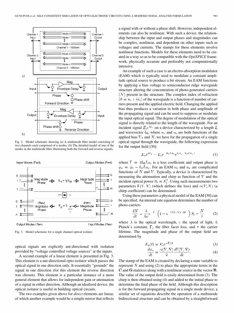
In order to illustrate the modeling of a direct element, amultimode fiber is taken as an example. This model uses delayelements, attenuation and phase-shifters to model the behaviorof a multimode fiber and follows the work in [29]. Detailsof this model are shown in Fig. 2. The first figure shows thesignal organization for the fiber with two channels. Within eachchannel there are optical modes present and each modeis bidirectional. Where is chosen to be large enough toaccurately model the optical field. The second figure shows adetailed model of one of the modes in a channel. This figureillustrates how the two state variables are connected. Themagnitude of each mode is isolated, attenuated and delayed.The delayed magnitude represents an envelope delay that couldvary from nanoseconds to seconds depending on the length ofthe element. The implementation of this delay makes uses ofthe stored history of the element and the known delay for eachmode in the fiber. The second state variable (phase) is passedthrough the element with the addition of a phase shift whichrepresents the shift of the phase from the input to the output.The magnitude of these delays is determined from the lengthof the fiber and the effective index of each mode. In this model,the total delay of the signal is therefore split into two parts, anenvelope delay and a phase delay. Envelope and phase delaysare uniquely specified for every mode in the fiber. The envelopedelay is calculated by determining the total phase delay presentfor a mode and then associating an integral number of phasedelays with this delay. The remainder of the phase delay (whichmust be between 0 and ) is used as the phase shift for themode. As can be seen in the figure the forward and reverse
GUNUPUDI et al.: SELF-CONSISTENT SIMULATION OF OPTO-ELECTRONIC CIRCUITS USING A MODIFIED NODAL ANALYSIS FORMULATION 983
Fig. 2. Model schematic showing (a) A multimode fiber model consisting oftwo channels each comprised of n modes. (b) The detailed model of one of themodes in the multimode fiber illustrating both the forward and reverse signals.
Fig. 3. Model schematic for a single channel optical isolater.
optical signals are explicitly uni-directional with isolationprovided by “voltage controlled voltage sources” at the inputs.
A second example of a linear element is presented in Fig. 3.This element is a uni-directional opto-isolator which passes theoptical signal in one direction only. It essentially “grounds” thesignal in one direction (for this element the reverse directionwas chosen). This element is a particular instance of a moregeneral element that allows for independent gain or attenuationof a signal in either direction. Although an idealized device, theoptical isolator is useful in building optical circuits.
The two examples given above for direct elements are linear,of which another example would be a simple mirror that reflects
a signal with or without a phase shift. However, independent el-ements can also be nonlinear. With such a device, the relation-ship between the input and output phases and magnitudes canbe complex, nonlinear, and dependent on other inputs such asvoltages and currents. The stamps for these elements involvenonlinear functions. Models for these elements need to be cre-ated in a way so as to be compatible with the OptiSPICE frame-work, physically accurate and preferably not computationallyintensive.
An example of such a case is an electro-absorption modulator(EAM) which is typically used to modulate a constant ampli-tude optical source to produce a bit stream. An EAM functionsby applying a bias voltage to semiconductor ridge waveguidestructure altering the concentration of photo-generated carriers
present in the structure. The complex index of refractionof the waveguide is a function of number of car-
riers present and the applied electric field. Changing the appliedbias thus produces a variation in both phase and amplitude ofthe propagating signal and can be used to suppress or modulatethe input optical signal. The degree of modulation of the opticalsignal is directly related to the length of the waveguide. For anincident signal on a device characterized by a lengthand wavevector , where and are both functions of theapplied bias and , we have for the propagation of a singleoptical signal through the waveguide, the following expressionfor the output field [30]:
(1)
where is a loss coefficient and output phase is. For an EAM and are complicated
functions of and . Typically, a device is characterized bymeasuring the attenuation and chirp as function of and theincident optical power . Using such measurements twoparameters (which defines the loss) and (achirp coefficient) can be determined.
Using these parameters a physical model of the EAM [30] canbe specified. An internal rate equation determines the number ofphoto-carriers
(2)
where is the optical wavelength, the speed of light,Planck’s constant, the fiber facet loss, and the carrierlifetime. The magnitude and phase of the output field aredetermined by
(3)
(4)
The stamp of the EAM is created by declaring a state variable torepresent and using (2) to place the appropriate terms in the
and matrices along with a nonlinear source in the vector .The value of the output field is easily determined from (3). Thechirp is then obtained using (4) and added to the initial phase todetermine the final phase of the field. Although this descriptionis for the forward propagating signal in a single mode device, asimilar set of equations describe the operation of a multimodebidirectional structure and can be obtained by a straightforward

984 IEEE TRANSACTIONS ON ADVANCED PACKAGING, VOL. 33, NO. 4, NOVEMBER 2010
Fig. 4. Model schematic for a single channel Electro Optical Absorber.
extension. The electrical submodel used for the EAM is a diodeor open circuit with an optional input circuit consisting of a re-sistor, inductor and capacitor. A schematic model of the deviceis presented in Fig. 4.
B. Optical Sources and Detectors
Two types of sources were implemented using the OptiSPICEinfrastructure. The first is a diode laser (DL) and the secondis a simple fictitious source referred to as constant wave (CW)source defined for convenience. The CW source can be used tofeed waveforms into optical components without the need for adiode laser and its driver circuit.
Diode Laser: The diode laser source is modeled in detail inthe OptiSPICE framework using its physical, electrical and op-tical device equations. A physically based model of a (singlemode for simplicity) laser diode can be defined using rate equa-tions for the electron and photon densities and optical phase[31], [32]
(5)
(6)
(7)
where is the injection efficiency, the diode current, thelaser volume, the number of carriers, and are the elec-tron and hole lifetimes, the gain coefficient, the photondensity, the mode confinement factor, the spontaneous emis-sion coefficient, the linewidth enhancement factor, and thegain compression coefficient. Following [32], a temperature de-pendent offset current defined by a polynomial
(8)
accounts for static thermal effects with the coefficientsdetermined from parameter extraction.
A schematic showing the internal details of the laser model ispresented in Fig. 5. The laser thus consists of a diode, three rate
Fig. 5. Model schematic for a single mode laser.
Fig. 6. Model schematic for a single channel multimode photodiode.
equations, and a thermal subcircuit. This laser model is tem-perature dependent and models a wide variety of effects. Theresulting model has internal state variables for photon density,carrier density, and device temperature. The output is an opticalfield magnitude and phase. Using these variables, the rate equa-tions governing the laser diode’s behaviour are stamped into theMNA matrices.
CW Source: The CW source has a defining carrier frequencyand two electrical ports that determine the magnitude and phaseof the optical output. The source can be operated in a number ofmodes. The simplest implementation linearly relates each inputvoltage to the two optical output variables of phase and magni-tude—in this mode the device is linear. When using the secondmode the two voltage inputs control the phase and the output op-tical power and the device is nonlinear with respect to the mag-nitude but linear for the phase variable. For the third mode theelectrical inputs are linearly related to the output field compo-nents and and in this case both optical outputs are nonlin-early related to the inputs. The CW source can be used in eithersingle mode or multimode operation and can be specified to beproduce singly or doubly polarized optical signals.
Photodiodes: Detectors are modeled using an electrical diodeand a photo-current which is proportional to the optical intensityat the input. The relationship of the photo-current to the opticalintensity is given by a frequency domain filter response [33] thatis synthesized into a circuit. In the implementation (shown inFig. 6) a set of nonlinear current sources each having a magni-tude determined by the square of the electric field magnitude as-sociated with an optical input mode are summed by connectingthem to a 1- resistor. The resultant voltage across this resistorhas the value and is then passed through the filter to obtaina voltage equal to the photo-current. This voltage then drives
GUNUPUDI et al.: SELF-CONSISTENT SIMULATION OF OPTO-ELECTRONIC CIRCUITS USING A MODIFIED NODAL ANALYSIS FORMULATION 985
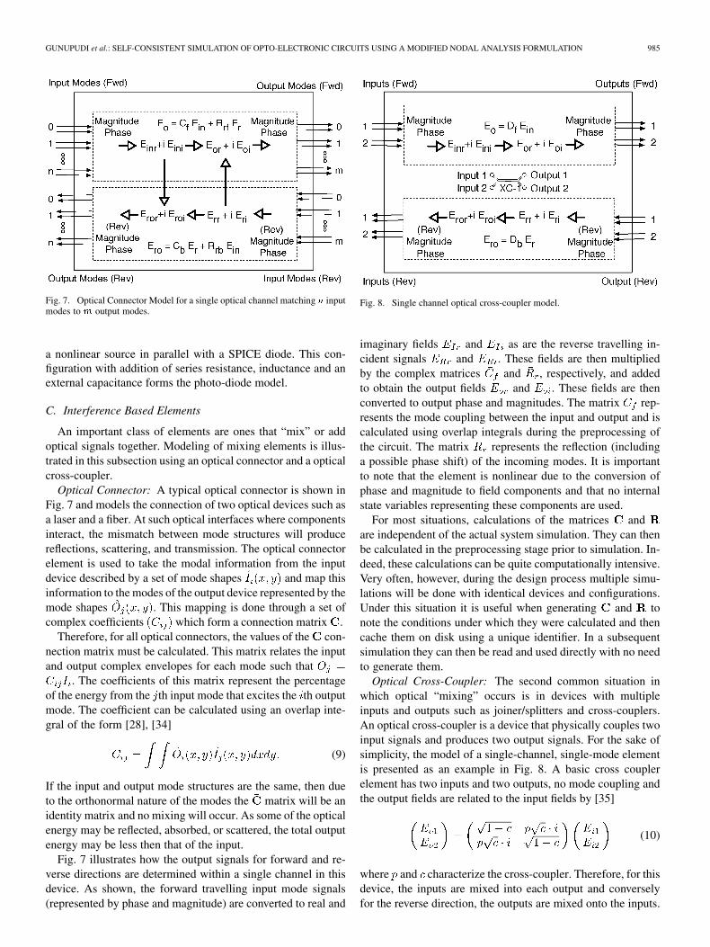
Fig. 7. Optical Connector Model for a single optical channel matching � inputmodes to � output modes.
a nonlinear source in parallel with a SPICE diode. This con-figuration with addition of series resistance, inductance and anexternal capacitance forms the photo-diode model.
C. Interference Based Elements
An important class of elements are ones that “mix” or addoptical signals together. Modeling of mixing elements is illus-trated in this subsection using an optical connector and a opticalcross-coupler.
Optical Connector: A typical optical connector is shown inFig. 7 and models the connection of two optical devices such asa laser and a fiber. At such optical interfaces where componentsinteract, the mismatch between mode structures will producereflections, scattering, and transmission. The optical connectorelement is used to take the modal information from the inputdevice described by a set of mode shapes and map thisinformation to the modes of the output device represented by themode shapes . This mapping is done through a set ofcomplex coefficients which form a connection matrix .
Therefore, for all optical connectors, the values of the con-nection matrix must be calculated. This matrix relates the inputand output complex envelopes for each mode such that
. The coefficients of this matrix represent the percentageof the energy from the th input mode that excites the th outputmode. The coefficient can be calculated using an overlap inte-gral of the form [28], [34]
(9)
If the input and output mode structures are the same, then dueto the orthonormal nature of the modes the matrix will be anidentity matrix and no mixing will occur. As some of the opticalenergy may be reflected, absorbed, or scattered, the total outputenergy may be less then that of the input.
Fig. 7 illustrates how the output signals for forward and re-verse directions are determined within a single channel in thisdevice. As shown, the forward travelling input mode signals(represented by phase and magnitude) are converted to real and
Fig. 8. Single channel optical cross-coupler model.
imaginary fields and as are the reverse travelling in-cident signals and . These fields are then multipliedby the complex matrices and , respectively, and addedto obtain the output fields and . These fields are thenconverted to output phase and magnitudes. The matrix rep-resents the mode coupling between the input and output and iscalculated using overlap integrals during the preprocessing ofthe circuit. The matrix represents the reflection (includinga possible phase shift) of the incoming modes. It is importantto note that the element is nonlinear due to the conversion ofphase and magnitude to field components and that no internalstate variables representing these components are used.
For most situations, calculations of the matrices andare independent of the actual system simulation. They can thenbe calculated in the preprocessing stage prior to simulation. In-deed, these calculations can be quite computationally intensive.Very often, however, during the design process multiple simu-lations will be done with identical devices and configurations.Under this situation it is useful when generating and tonote the conditions under which they were calculated and thencache them on disk using a unique identifier. In a subsequentsimulation they can then be read and used directly with no needto generate them.
Optical Cross-Coupler: The second common situation inwhich optical “mixing” occurs is in devices with multipleinputs and outputs such as joiner/splitters and cross-couplers.An optical cross-coupler is a device that physically couples twoinput signals and produces two output signals. For the sake ofsimplicity, the model of a single-channel, single-mode elementis presented as an example in Fig. 8. A basic cross couplerelement has two inputs and two outputs, no mode coupling andthe output fields are related to the input fields by [35]
(10)
where and characterize the cross-coupler. Therefore, for thisdevice, the inputs are mixed into each output and converselyfor the reverse direction, the outputs are mixed onto the inputs.
986 IEEE TRANSACTIONS ON ADVANCED PACKAGING, VOL. 33, NO. 4, NOVEMBER 2010
Fig. 9. Optical circulator formed as a complex element.
This mixing is represented by the matrices and whichperform the mixing for all modes in the channel and are createdby applying the relationship presented in (10).
An optical splitter/joiner can also be implemented in such astructure. For example for a 3 db splitter/joiner that conservespower, having one input and two outputs, the relationship be-tween the forward travelling waves for the two output fields andthe input would be
(11)
and in the backwards direction
(12)
The examples of mixing elements illustrated above are spe-cific instances of a generalized signal-mixing element imple-mented in OptiSPICE. This element allows the linear mixing ofoptical fields from inputs with modes to outputs with
modes. This generalized element allows for a very generallinear mixing of multiple inputs and outputs modes and signalreflections. It can also be used to define linear gain/attenua-tion elements, to characterize optical loss and model diffractionthrough free space regions. When this device is implemented, ithas to be treated as a nonlinear element due to the presence oftrigonometric functions. However, derivatives of these trigono-metric functions are well-behaved and work well within theNewton–Raphson nonlinear solver used in the engine. One com-plication, as mentioned before, is that the output phases deter-mined by are band limited to to and care must be takento make the output phase continuous by keeping track of thenumber of traversals that have undergone during the tran-sient simulation.
D. Complex Elements
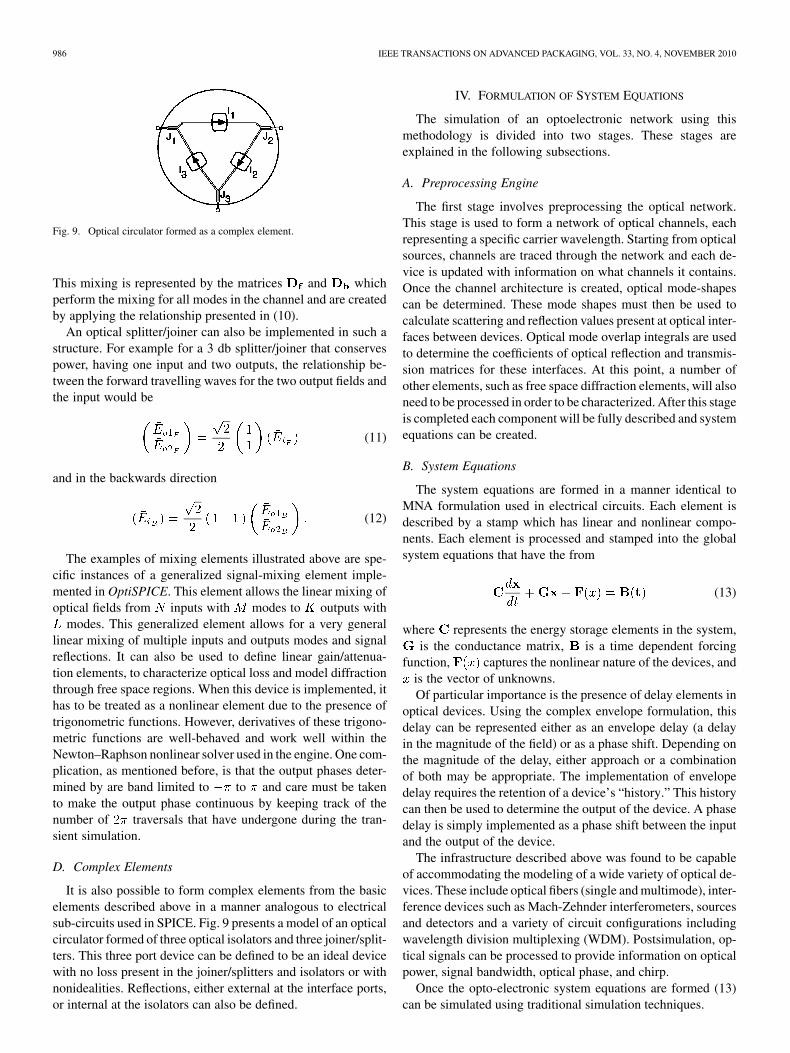
It is also possible to form complex elements from the basicelements described above in a manner analogous to electricalsub-circuits used in SPICE. Fig. 9 presents a model of an opticalcirculator formed of three optical isolators and three joiner/split-ters. This three port device can be defined to be an ideal devicewith no loss present in the joiner/splitters and isolators or withnonidealities. Reflections, either external at the interface ports,or internal at the isolators can also be defined.
IV. FORMULATION OF SYSTEM EQUATIONS
The simulation of an optoelectronic network using thismethodology is divided into two stages. These stages areexplained in the following subsections.
A. Preprocessing Engine
The first stage involves preprocessing the optical network.This stage is used to form a network of optical channels, eachrepresenting a specific carrier wavelength. Starting from opticalsources, channels are traced through the network and each de-vice is updated with information on what channels it contains.Once the channel architecture is created, optical mode-shapescan be determined. These mode shapes must then be used tocalculate scattering and reflection values present at optical inter-faces between devices. Optical mode overlap integrals are usedto determine the coefficients of optical reflection and transmis-sion matrices for these interfaces. At this point, a number ofother elements, such as free space diffraction elements, will alsoneed to be processed in order to be characterized. After this stageis completed each component will be fully described and systemequations can be created.
B. System Equations
The system equations are formed in a manner identical toMNA formulation used in electrical circuits. Each element isdescribed by a stamp which has linear and nonlinear compo-nents. Each element is processed and stamped into the globalsystem equations that have the from
(13)
where represents the energy storage elements in the system,is the conductance matrix, is a time dependent forcing
function, captures the nonlinear nature of the devices, andis the vector of unknowns.Of particular importance is the presence of delay elements in
optical devices. Using the complex envelope formulation, thisdelay can be represented either as an envelope delay (a delayin the magnitude of the field) or as a phase shift. Depending onthe magnitude of the delay, either approach or a combinationof both may be appropriate. The implementation of envelopedelay requires the retention of a device’s “history.” This historycan then be used to determine the output of the device. A phasedelay is simply implemented as a phase shift between the inputand the output of the device.
The infrastructure described above was found to be capableof accommodating the modeling of a wide variety of optical de-vices. These include optical fibers (single and multimode), inter-ference devices such as Mach-Zehnder interferometers, sourcesand detectors and a variety of circuit configurations includingwavelength division multiplexing (WDM). Postsimulation, op-tical signals can be processed to provide information on opticalpower, signal bandwidth, optical phase, and chirp.
Once the opto-electronic system equations are formed (13)can be simulated using traditional simulation techniques.
GUNUPUDI et al.: SELF-CONSISTENT SIMULATION OF OPTO-ELECTRONIC CIRCUITS USING A MODIFIED NODAL ANALYSIS FORMULATION 987
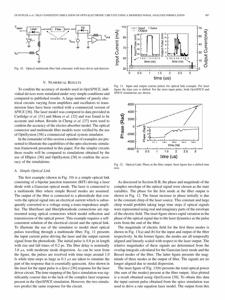
Fig. 10. Optical multimode fiber link schematic with laser driver and detector.
V. NUMERICAL RESULTS
To confirm the accuracy of models used in OptiSPICE, indi-vidual devices were simulated under very simple conditions andcompared to published results. A large number of purely elec-trical circuits varying from amplifiers and oscillators to trans-mission lines have been verified with a commercial version ofSPICE [36]. The laser model was compared to data provided inCartlidge et al. [31] and Mena et al. [32] and was found to beaccurate and robust. Results in Cheng et al. [37] were used toconfirm the accuracy of the electro-absorber model. The opticalconnector and multimode fiber models were verified by the useof OptiSystem [38] a commercial optical system simulator.
In the remainder of this section a number of examples are pre-sented to illustrate the capabilities of the opto-electronic simula-tion framework presented in this paper. For the simpler circuitsthese results will be compared to simulations obtained by theuse of HSpice [36] and OptiSystem [38] to confirm the accu-racy of the simulations.
A. Simple Optical Link
The first example (shown in Fig. 10) is a simple optical linkconsisting of a bipolar junction transistor (BJT) driving a laserdiode with a Gaussian optical mode. The laser is connected toa multimode fiber where simple Bessel modes are assumed.The output of the fiber is connected to a photodiode that con-verts the optical signal into an electrical current which is subse-quently converted to a voltage using a trans-impedence ampli-fier. The fiber/laser and fiber/photodiode connections are rep-resented using optical connectors which model reflection andtransmission of the optical power. This example requires a self-consistent solution of the electrical circuit and the optical link.To illustrate the use of the simulator to model short opticalpulses travelling through a multimode fiber, Fig. 11 presentsthe input current pulse driving the laser and the output currentsignal from the photodiode. The initial pulse is 0.8 ps in lengthwith rise and fall times of 0.2 ps. The fiber delay is nominally3.0 s, with moderate mode dispersion. As can be seen fromthe figure, the pulses are resolved with time-steps around 1.0fs while time-steps as large as 0.1 s are taken to simulate thepart of the response that is essentially quiescent. Also shown inthe inset for the input pulse is a Spice [36] response for the laserdriver circuit. The time stepping of the Spice simulation was sig-nificantly coarser due to the lack of the complex laser responsepresent in the OptiSPICE simulation. However, the two simula-tors predict the same response for the circuit.
Fig. 11. Input and output current pulses for optical link example. For insetfigure the time axis is shifted. For the inset input pulse, both OptiSPICE andSPICE simulations are shown.
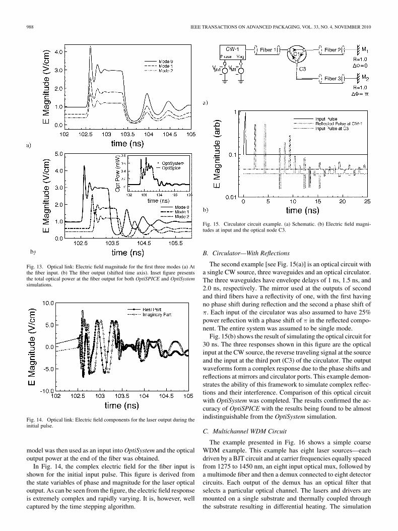
Fig. 12. Optical Link: Phase at the fiber output. Inset figure has a shifted timeaxis.
As discussed in Section II-B, the phase and magnitude of thecomplex envelope of the optical signal were chosen as the statevariables. The phase for the first mode at the fiber output isshown in Fig. 12. The linear increase in phase initially is dueto the constant chirp of the laser source. This constant and largechirp would prohibit taking large time steps if optical signalswere represented using real and imaginary parts of the envelopeof the electric field. The inset figure shows rapid variation in thephase of the optical signal due to the laser dynamics as the pulseexits from the end of the fiber.
The magnitude of electric field for the first three modes isshown in Fig. 13(a) and (b) for the input and output of the fiberrespectively. In the former figure, the modes are all temporallyaligned and linearly scaled with respect to the laser output. Therelative magnitudes of these signals are determined from theoverlap integrals calculated for the Gaussian laser mode and theBessel modes of the fiber. The latter figure presents the mag-nitude of three modes at the output of fiber. The signals are nolonger aligned due to modal dispersion.
The inset figure of Fig. 13(b) presents the total optical power(the sum of the modes) present at the fiber output. Also plottedis a result obtained using OptiSystem [38]. To obtain this datathe input current pulse obtained from the spice simulation wasused to drive a rate equation laser model. The output from this
988 IEEE TRANSACTIONS ON ADVANCED PACKAGING, VOL. 33, NO. 4, NOVEMBER 2010
Fig. 13. Optical link: Electric field magnitude for the first three modes (a) Atthe fiber input. (b) The fiber output (shifted time axis). Inset figure presentsthe total optical power at the fiber output for both OptiSPICE and OptiSystemsimulations.
Fig. 14. Optical link: Electric field components for the laser output during theinitial pulse.
model was then used as an input into OptiSystem and the opticaloutput power at the end of the fiber was obtained.
In Fig. 14, the complex electric field for the fiber input isshown for the initial input pulse. This figure is derived fromthe state variables of phase and magnitude for the laser opticaloutput. As can be seen from the figure, the electric field responseis extremely complex and rapidly varying. It is, however, wellcaptured by the time stepping algorithm.
Fig. 15. Circulator circuit example. (a) Schematic. (b) Electric field magni-tudes at input and the optical node C3.
B. Circulator—With Reflections
The second example [see Fig. 15(a)] is an optical circuit witha single CW source, three waveguides and an optical circulator.The three waveguides have envelope delays of 1 ns, 1.5 ns, and2.0 ns, respectively. The mirror used at the outputs of secondand third fibers have a reflectivity of one, with the first havingno phase shift during reflection and the second a phase shift of
. Each input of the circulator was also assumed to have 25%power reflection with a phase shift of in the reflected compo-nent. The entire system was assumed to be single mode.
Fig. 15(b) shows the result of simulating the optical circuit for30 ns. The three responses shown in this figure are the opticalinput at the CW source, the reverse traveling signal at the sourceand the input at the third port (C3) of the circulator. The outputwaveforms form a complex response due to the phase shifts andreflections at mirrors and circulator ports. This example demon-strates the ability of this framework to simulate complex reflec-tions and their interference. Comparison of this optical circuitwith OptiSystem was completed. The results confirmed the ac-curacy of OptiSPICE with the results being found to be almostindistinguishable from the OptiSystem simulation.
C. Multichannel WDM Circuit
The example presented in Fig. 16 shows a simple coarseWDM example. This example has eight laser sources—eachdriven by a BJT circuit and at carrier frequencies equally spacedfrom 1275 to 1450 nm, an eight input optical mux, followed bya multimode fiber and then a demux connected to eight detectorcircuits. Each output of the demux has an optical filter thatselects a particular optical channel. The lasers and drivers aremounted on a single substrate and thermally coupled throughthe substrate resulting in differential heating. The simulation
GUNUPUDI et al.: SELF-CONSISTENT SIMULATION OF OPTO-ELECTRONIC CIRCUITS USING A MODIFIED NODAL ANALYSIS FORMULATION 989
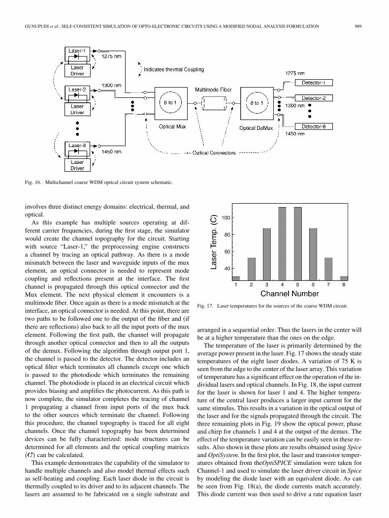
Fig. 16. Multichannel coarse WDM optical circuit system schematic.
involves three distinct energy domains: electrical, thermal, andoptical.
As this example has multiple sources operating at dif-ferent carrier frequencies, during the first stage, the simulatorwould create the channel topography for the circuit. Startingwith source “Laser-1,” the preprocessing engine constructsa channel by tracing an optical pathway. As there is a modemismatch between the laser and waveguide inputs of the muxelement, an optical connector is needed to represent modecoupling and reflections present at the interface. The firstchannel is propagated through this optical connector and theMux element. The next physical element it encounters is amultimode fiber. Once again as there is a mode mismatch at theinterface, an optical connector is needed. At this point, there aretwo paths to be followed one to the output of the fiber and (ifthere are reflections) also back to all the input ports of the muxelement. Following the first path, the channel will propagatethrough another optical connector and then to all the outputsof the demux. Following the algorithm through output port 1,the channel is passed to the detector. The detector includes anoptical filter which terminates all channels except one whichis passed to the photodiode which terminates the remainingchannel. The photodiode is placed in an electrical circuit whichprovides biasing and amplifies the photocurrent. As this path isnow complete, the simulator completes the tracing of channel1 propagating a channel from input ports of the mux backto the other sources which terminate the channel. Followingthis procedure, the channel topography is traced for all eightchannels. Once the channel topography has been determineddevices can be fully characterized: mode structures can bedetermined for all elements and the optical coupling matrices
can be calculated.This example demonstrates the capability of the simulator to
handle multiple channels and also model thermal effects suchas self-heating and coupling. Each laser diode in the circuit isthermally coupled to its driver and to its adjacent channels. Thelasers are assumed to be fabricated on a single substrate and
Fig. 17. Laser temperatures for the sources of the coarse WDM circuit.
arranged in a sequential order. Thus the lasers in the center willbe at a higher temperature than the ones on the edge.
The temperature of the laser is primarily determined by theaverage power present in the laser. Fig. 17 shows the steady statetemperatures of the eight laser diodes. A variation of 75 K isseen from the edge to the center of the laser array. This variationof temperature has a significant effect on the operation of the in-dividual lasers and optical channels. In Fig. 18, the input currentfor the laser is shown for laser 1 and 4. The higher tempera-ture of the central laser produces a larger input current for thesame stimulus. This results in a variation in the optical output ofthe laser and for the signals propagated through the circuit. Thethree remaining plots in Fig. 19 show the optical power, phaseand chirp for channels 1 and 4 at the output of the demux. Theeffect of the temperature variation can be easily seen in these re-sults. Also shown in these plots are results obtained using Spiceand OptiSystem. In the first plot, the laser and transistor temper-atures obtained from theOptiSPICE simulation were taken forChannel-1 and used to simulate the laser driver circuit in Spiceby modeling the diode laser with an equivalent diode. As canbe seen from Fig. 18(a), the diode currents match accurately.This diode current was then used to drive a rate equation laser

990 IEEE TRANSACTIONS ON ADVANCED PACKAGING, VOL. 33, NO. 4, NOVEMBER 2010
Fig. 18. Coarse WDM example. Transient plots for channels 1 and 4: (a) Inputlaser currents. (b) Output laser optical powers.
model in OptiSystem; which then provided an optical signal foran OptiSystem simulation of the optical link. In the plots ofoptical power, phase and chirp (Fig. 18(b) and Fig. 19) it canbe seen that OptiSPICE matches the OptiSystem results accu-rately. Modeling the whole system using Spice and OptiSystem,although doable, would be cumbersome due to the need to pro-vide a convergence between the thermal coupling (which is non-linear), the laser rate equations and the electrical simulation ofall eight drivers and laser diodes.
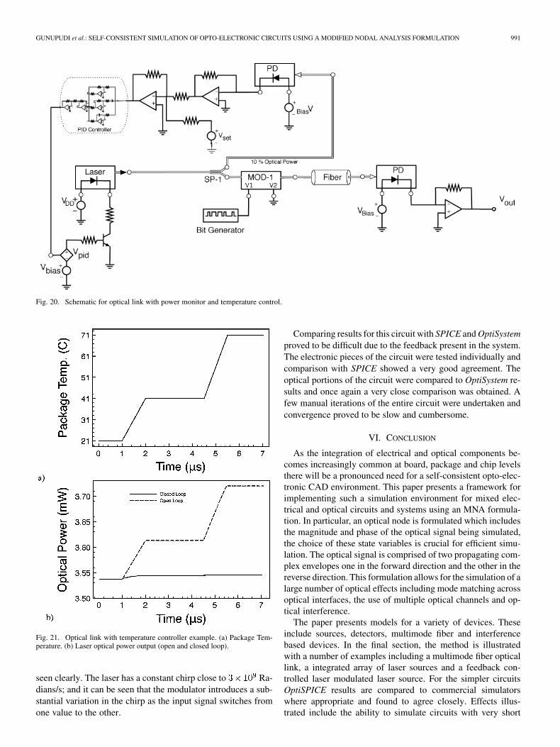
D. PID Controller Example
The final example (see Fig. 20) shows a tightly coupled opto-electronic circuit—with feedback control on the optical output.This circuit consists of an optical link from source to detector;however, in this case the CW optical output is modulated ex-ternally by an electrooptic modulator. The optical signal pro-vided by the laser is desired to be as independent of externalphenomena as possible. To achieve this a proportional-integral-derivative (PID) controller is used. A small percentage of theoptical power is split off from the output of the laser and is fedto a photodetector. The output from this detector is used as theinput to a closed loop PID controller that adjusts the bias of thelaser driver so as to keep the output power at a set-point.
Typically, the external disturbance would be in the form ofa change in the ambient temperature. The feedback loop wouldadjust the bias voltage accordingly to compensate for the tem-perature change and keep the laser power constant. This circuit
Fig. 19. Coarse WDM example. Transient plots for channels 1 and 4: (a) Op-tical phase and (b) Laser chirp.
has two extremely different time scales. The thermal behavior ofthe device and the response of the PID controller are character-ized by time constants in the microseconds or even milliseconds.On the other hand the data pulses in the system are typically innanoseconds.
The plots in Fig. 21 show the operation of the PID feed-back control. The temperature of the laser and bias circuitrywas determined by a thermal subcircuit driven by a timedependent source representing an externally fluctuating sub-strate temperature. This temperature variation is shown inFig. 21(a). The response of the laser output power is presentedin Fig. 21(b). Responses for two cases are shown—open andclosed loop cases. As expected, closing the PID feedbackloop causes the laser bias to be adjusted to compensate for thetemperature changes.
A second set of plots presented in Fig. 22 show the responseof this circuit over a much smaller time scale. In this figure,the temperature of the circuit is essentially constant, however, apseudo-random bit stream is used to bias the electrooptic mod-ulator. The voltage input to the modulator is shown in Fig. 22(a)with 15 bits. The output power of the modulator can be seen inFig. 22(b) showing the complex pulse shape produced by thenonlinearity of the modulator and the ringing behaviour in thevoltage input due to lead inductance and capacitance. Finally,Fig. 22(c) presents the chirp (determined from the phase of theoutput) introduced in the optical signal by the modulator. It isimportant to model modulator chirp and in this case, it can be
GUNUPUDI et al.: SELF-CONSISTENT SIMULATION OF OPTO-ELECTRONIC CIRCUITS USING A MODIFIED NODAL ANALYSIS FORMULATION 991
Fig. 20. Schematic for optical link with power monitor and temperature control.
Fig. 21. Optical link with temperature controller example. (a) Package Tem-perature. (b) Laser optical power output (open and closed loop).
seen clearly. The laser has a constant chirp close to Ra-dians/s; and it can be seen that the modulator introduces a sub-stantial variation in the chirp as the input signal switches fromone value to the other.
Comparing results for this circuit with SPICE and OptiSystemproved to be difficult due to the feedback present in the system.The electronic pieces of the circuit were tested individually andcomparison with SPICE showed a very good agreement. Theoptical portions of the circuit were compared to OptiSystem re-sults and once again a very close comparison was obtained. Afew manual iterations of the entire circuit were undertaken andconvergence proved to be slow and cumbersome.
VI. CONCLUSION
As the integration of electrical and optical components be-comes increasingly common at board, package and chip levelsthere will be a pronounced need for a self-consistent opto-elec-tronic CAD environment. This paper presents a framework forimplementing such a simulation environment for mixed elec-trical and optical circuits and systems using an MNA formula-tion. In particular, an optical node is formulated which includesthe magnitude and phase of the optical signal being simulated,the choice of these state variables is crucial for efficient simu-lation. The optical signal is comprised of two propagating com-plex envelopes one in the forward direction and the other in thereverse direction. This formulation allows for the simulation of alarge number of optical effects including mode matching acrossoptical interfaces, the use of multiple optical channels and op-tical interference.
The paper presents models for a variety of devices. Theseinclude sources, detectors, multimode fiber and interferencebased devices. In the final section, the method is illustratedwith a number of examples including a multimode fiber opticallink, a integrated array of laser sources and a feedback con-trolled laser modulated laser source. For the simpler circuitsOptiSPICE results are compared to commercial simulatorswhere appropriate and found to agree closely. Effects illus-trated include the ability to simulate circuits with very short

992 IEEE TRANSACTIONS ON ADVANCED PACKAGING, VOL. 33, NO. 4, NOVEMBER 2010
Fig. 22. Optical link with temperature controller example. Modulation resultsusing an Electro-Absorption Modulator. (a) Input voltage. (b) Optical outputpower. (c) Optical output chirp.
pulses and significant fiber optical delays, pulse reflection andinterference, thermal effects, and self-consistent simulationencompassing the electrical, thermal, and optical domains.
REFERENCES
[1] R. Nagarajan, C. Joyner, J. Schneider, R. P. , J. Bostak, T. Butrie, A.Dentai, V. Dominic, P. Evans, M. Kato, M. Kauffman, D. Lambert,S. Mathis, A. Mathur, R. Miles, M. Mitchell, M. Missey, S. Murthy,A. Nilsson, F. Peters, S. Pennypacker, J. Pleumeekers, R. Salvatore,R. Schlenker, R. Taylor, H.-S. Tsai, M. Van Leeuwen, J. Webjorn, M.Ziari, D. Perkins, J. Singh, S. Grubb, M. Reffle, D. Mehuys, F. Kish,and D. Welch, “Large-scale photonic integrated circuits,” IEEE Trans.Sel. Topics Quantum Electron., vol. 11, no. 1, pp. 50–65, Jan.–Feb.2005.
[2] Z. Mi, J. Yang, P. Bhattacharya, G. Qin, and Z. Ma, “High-performancequantum dot lasers and integrated optoelectronics on si,” Proc. IEEE,vol. 97, no. 7, pp. 1239–1249, Jul. 2009.
[3] Z. Yuan, A. Anopchenko, N. Daldosso, R. Guider, D. Navarro-Urrios,A. Pitanti, R. Spano, and L. Pavesi, “Silicon nanocrystals as an en-abling material for silicon photonics,” Proc. IEEE, vol. 97, no. 7, pp.1250–1268, Jul. 2009.
[4] J. Leuthold, W. Freude, J.-M. Brosi, R. Baets, P. Dumon, I. Biaggio, M.Scimeca, F. Diederich, B. Frank, and C. Koos, “Silicon organic hybridtechnology platform for practical nonlinear optics,” Proc. IEEE, vol.97, no. 7, pp. 1304–1316, Jul. 2009.
[5] K. Ohashi, K. Nishi, T. Shimizu, M. Nakada, J. Fujikata, J. Ushida, S.Torii, K. Nose, M. Mizuno, H. Yukawa, M. Kinoshita, N. Suzuki, A.Gomyo, T. Ishi, D. Okamoto, K. Furue, T. Ueno, T. Tsuchizawa, T.Watanabe, K. Yamada, S.-I. Itabashi, and J. Akedo, “On-chip opticalinterconnect,” Proc. IEEE, vol. 97, no. 7, pp. 1186–1198, Jul. 2009.
[6] R. Tummala, “Sop: What is it and why? A new microsystem-inte-gration technology paradigm-Moore’s law for system integration ofminiaturized convergent systems of the next decade,” IEEE Trans. Adv.Packag., vol. 27, no. 2, pp. 241–249, May 2004.
[7] M. Iyer, P. Ramana, K. Sudharsanam, C. Leo, M. Sivakumar, B. L. S.Pong, and X. Ling, “Design and development of optoelectronic mixedsignal system-on-package (sop),” IEEE Trans. Adv. Packag., vol. 27,no. 2, pp. 278–285, May 2004.
[8] J. Minz, S. Thyagara, and S. K. Lim, “Optical routing for 3-dsystem-on-package,” IEEE Trans. Compon. Packag. Technol., vol. 30,no. 4, pp. 805–812, Dec. 2007.
[9] G.-K. Chang, D. Guidotti, F. Liu, Y.-J. Chang, Z. Huang, V. Sundaram,D. Balaraman, S. Hegde, and R. Tummala, “Chip-to-chip optoelec-tronics sop on organic boards or packages,” IEEE Trans. Adv. Packag.,vol. 27, no. 2, pp. 386–397, May 2004.
[10] R. Soref, “Silicon-based optoelectronics,” Proc. IEEE, vol. 81, no. 12,pp. 1687–1706, Dec. 1993.
[11] R. Soref, “The past, present, and future of silicon photonics,” IEEETrans. Sel. Topics Quantum Electron., vol. 12, no. 6, pp. 1678–1687,Nov.–Dec. 2006.
[12] L. Tsybeskov, D. Lockwood, and M. Ichikawa, “Silicon photonics:CMOS going optical,” Proc. IEEE, vol. 97, no. 7, pp. 1161–1165, Jul.2009.
[13] K. Wada, S. Park, and Y. Ishikawa, “Si photonics and fiber to thehome,” Proc. IEEE, vol. 97, no. 7, pp. 1329–1336, Jul. 2009.
[14] A. Krishnamoorthy, R. Ho, X. Zheng, H. Schwetman, J. Lexau, P.Koka, G. Li, I. Shubin, and J. Cunningham, “Computer systems basedon silicon photonic interconnects,” Proc. IEEE, vol. 97, no. 7, pp.1337–1361, Jul. 2009.
[15] G. Agrawal, Fiber-Optic Communication Systems. New York: Wiley, 2003.
[16] C. DeCusatis, Fiber Optic Data Communication. New York: Else-vier, 2008.
[17] M. Neifeld and W. Chou, “Spice-based optoelectronic system simula-tion,” Appl. Opt., vol. 37, no. 26, pp. 6093–6104, 1998.
[18] S. Ozyazici and N. Dogru, “Ultrashort pulse generation by spice simu-lation of gain switching in quantum well laser,” in Conf. Lasers Electro-Optics—Pacific Rim, 2007 (CLEO/Pacific Rim 2007), Aug. 2007, pp.1–2.
[19] S.-W. Lee, E.-C. Choi, and W.-Y. Choi, “Optical interconnec-tion system analysis using spice,” in Pacific Rim Conf. Lasers andElectro-Optics, 1999 (CLEO/Pacific Rim’99), 1999, vol. 2, pp.391–392, vol. 2.
[20] B. Whitlock, J. Morikuni, E. Conforti, and S.-M. Kang, “Simulationand modeling: Simulating optical interconnects,” IEEE Circuits De-vices Mag., vol. 11, no. 3, pp. 12–18, May 1995.
[21] A. Yang and S. Kang, “ismile: A novel circuit simulation program withemphasis on new device model development,” in Proc. 26th Conf. De-sign Automat., Jun. 1989, pp. 630–633.
[22] S. Levitan, T. Kurzweg, P. Marchand, M. Rempel, D. Chiarulli, J. Mar-tinez, J. Bridgen, C. Fan, and F. McCormick, “Chatoyant: A com-puter-aided design tool for free-space optoelectronic systems,” Appl.Opt., vol. 37, no. 26, pp. 6078–6092, Sep. 1998.
[23] M. Kahrs, S. Levitan, D. Chiarulli, T. Kurzweg, J. Martinez, J. Boles,A. Davare, E. Jackson, C. Windish, F. Kiamilev, A. Bhaduri, M. Taufik,X. Wang, A. Morris, J. Kruchowski, and B. Gilbert, “System-levelmodeling and simulation of the 10 g optoelectronic interconnect,” J.Lightwave Technol., vol. 21, no. 12, pp. 3244–3256, Dec. 2003.
[24] J. Eker, J. Janneck, E. Lee, J. Liu, X. Liu, J. Ludvig, S. Neuendorffer, S.Sachs, and Y. Xiong, “Taming heterogeneity—The ptolemy approach,”Proc. IEEE, vol. 91, no. 1, pp. 127–144, Jan. 2003.
[25] T. Quarles, A. Newton, D. Pederson, and A. Sangiovanni-Vincentelli,SPICE 3 Version 3F5 User’s Manual Dept. EECE, Univ. California,Berkeley.

GUNUPUDI et al.: SELF-CONSISTENT SIMULATION OF OPTO-ELECTRONIC CIRCUITS USING A MODIFIED NODAL ANALYSIS FORMULATION 993
[26] C. Ho, A. Ruehli, and P. Brennan, “The modified nodal approach to net-work analysis,” Trans. on Circuits and Systems, vol. 22, pp. 504–509,Jun. 1975.
[27] J. D. Jackson, Classical Electrodynamics. New York: Academic,Aug. 1998, 2009, vol. 2009, no. 12.
[28] T. Tamir, Guided-Wave Optoelectronics. Berlin, Germany:Springer=Verlag, 1995.
[29] P. Pepeljugoski, S. E. Golowich, A. J. Ritger, P. Kolesar, and A. Ris-teski, “Modeling and simulation of next-generation multimode fiberlinks,” J. Lightwave Technol., vol. 21, pp. 1242–1255, May 2003.
[30] N. Cheng and J. Cartledge, “Measurement-based model for mqw elec-troabsorption modulators,” J. Lightwave Technol., vol. 23, no. 12, pp.4265–4269, Dec. 2005.
[31] J. C. Cartledge and R. C. Srinivasan, “Extraction of dfb laser rateequation parameters for system simulation purposes,” J. LightwaveTechnol., vol. 15, no. 5, pp. 852–860, Mar. 1997.
[32] P. V. Mena, J. J. Morikuni, S. M. Kang, A. V. Harton, and K. W.Wyatt, “A simple rate-equation-based thermal vcsel model,” J. Light-wave Technol., vol. 17, no. 5, pp. 865–872, May 1999.
[33] J. Campbell, B. Johnson, G. Qua, and W. Tsang, “Frequency responseof inp/ingaasp/ingaas avalanche photodiodes,” J. Lightwave Technol.,vol. 7, no. 5, pp. 778–784, May 1989.
[34] C.-L. Chen, Foundations for Guided-Wave Optics. New York: Wiley,2006.
[35] G. Keiser, Optical Fiber Communications. New York: McGraw-Hill,2000.
[36] SPICE [Online]. Available: http://www.synopsys.com/Tools/Verifica-tion/AMSVerification/CircuitSimulation/HSPICE
[37] C. N. and J. C. Cartledge, “Measurement-based model for mqw elec-troabsorption modulators,” J. Lightwave Technol., vol. 23, no. 12, pp.4165–4269, Dec. 2005.
[38] OptiSystem [Online]. Available: http://www.optiwave.com/products/system_overview.html
Pavan Gunupudi (S’97–M’02) received his B.Tech.degree from the Indian Institute of Technology,Chennai, India, in 1997, and the Ph.D. degree fromCarleton University, Ottawa, ON, Canada, in 2002.
He then joined the Department of Electronics atCarleton University and is presently an AssociateProfessor. His research interests include signalintegrity, high-speed VLSI systems, and multidisci-plinary simulation. He has authored more than 40journal and conference papers and is a co-author ofOptiSPICE.
Tom Smy received the B.Sc. and Ph.D. degrees inelectrical engineering from the University of Alberta,Edmonton, AB, Canada, in 1986 and 1990, respec-tively.
He is a Professor in the Department of Electronicsat Carleton University, Ottawa, ON, Canada. His cur-rent research interests include optical, thermal andmultiphysics simulation of electronic devices/pack-ages and modules, the study and simulation of thinfilm growth and microstructures, and a variety ofbackend processing projects. He has published over
100 journal papers and is a co-author of the OptiSPICE, Atar, SIMBAD, and3D-Films simulators.
Jackson Klein received the B.Sc. degree in elec-trical engineering from the Federal University ofSanta Maria, Brazil, in 1993, and the M.Sc. andPh.D. degrees in electrical engineering, in 1995 and1999, respectively, from UNICAMP, Brazil, and theM.B.A. degree from the University of Ottawa, ON,Canada.
He has been working with design and develop-ment of computer-aided design and analysis toolsfor optical communication systems for more than 15years. He joined Optiwave after receiving the Ph.D.
and since 1999 he has been part of the Research and Development Group atOptiwave Corporation as the Director of Optical Systems and one of the mainresearchers and designers of OptiSystem and OptiSPICE technologies. He isthe author of over 25 conference papers and technical articles.
Z. Jan Jakubczyk received the M.Sc. degree in engi-neering physics from the Silesian Technical Univer-sity, in 1976, and the Ph.D. degree from the Instituteof Fundamental Research, Warsaw, Poland, in 1984,and the MBA degree from the University of Ottawa,Canada, in 2004.
From 1976 to 1986 he was an Associate Professorat the Silesian Technical University. From 1986 to1988 he was a Research Associate at Laval Univer-sity, Quebec, Canada. From 1989 to 1994 he was aResearch Scientist at the National Optics Institute in
Quebec, Canada. His research activities included surface acoustic waves (SAW)applications and waveguide properties of photonic devices. In 1994, he foundedOptiwave Corporation where he is the CEO.
Related Documents