Subscriber access provided by - Access paid by the | UCLA Library Nano Letters is published by the American Chemical Society. 1155 Sixteenth Street N.W., Washington, DC 20036 Letter Self-Catalyzed Epitaxial Growth of Vertical Indium Phosphide Nanowires on Silicon Li Gao, Robyn L. Woo, Baolai Liang, Marta Pozuelo, Sergey Prikhodko, Mike Jackson, Niti Goel, Mantu K. Hudait, Diana L. Huffaker, Mark S. Goorsky, Suneel Kodambaka, and Robert F. Hicks Nano Lett., Article ASAP • DOI: 10.1021/nl803567v • Publication Date (Web): 04 May 2009 Downloaded from http://pubs.acs.org on May 6, 2009 More About This Article Additional resources and features associated with this article are available within the HTML version: • Supporting Information • Access to high resolution figures • Links to articles and content related to this article • Copyright permission to reproduce figures and/or text from this article

Welcome message from author
This document is posted to help you gain knowledge. Please leave a comment to let me know what you think about it! Share it to your friends and learn new things together.
Transcript

Subscriber access provided by - Access paid by the | UCLA Library
Nano Letters is published by the American Chemical Society. 1155 SixteenthStreet N.W., Washington, DC 20036
Letter
Self-Catalyzed Epitaxial Growth of VerticalIndium Phosphide Nanowires on Silicon
Li Gao, Robyn L. Woo, Baolai Liang, Marta Pozuelo, Sergey Prikhodko, Mike Jackson, Niti Goel,Mantu K. Hudait, Diana L. Huffaker, Mark S. Goorsky, Suneel Kodambaka, and Robert F. Hicks
Nano Lett., Article ASAP • DOI: 10.1021/nl803567v • Publication Date (Web): 04 May 2009
Downloaded from http://pubs.acs.org on May 6, 2009
More About This Article
Additional resources and features associated with this article are available within the HTML version:
• Supporting Information• Access to high resolution figures• Links to articles and content related to this article• Copyright permission to reproduce figures and/or text from this article
Self-Catalyzed Epitaxial Growth ofVertical Indium Phosphide Nanowires onSiliconLi Gao,† Robyn L. Woo,† Baolai Liang,‡ Marta Pozuelo,§ Sergey Prikhodko,§Mike Jackson,§ Niti Goel,| Mantu K. Hudait,⊥ Diana L. Huffaker,‡Mark S. Goorsky,§ Suneel Kodambaka,§ and Robert F. Hicks*,†,§
Department of Chemical and Biomolecular Engineering, Department of ElectricalEngineering, Department of Materials Science and Engineering, UniVersity ofCalifornia, Los Angeles, CA 90095, Intel Corporation, Santa Clara, CA 95052, andIntel Corporation, Hillsboro, OR 97124
Received November 24, 2008; Revised Manuscript Received April 17, 2009
ABSTRACT
Vertical indium phosphide nanowires have been grown epitaxially on silicon (111) by metalorganic vapor-phase epitaxy. Liquid indium dropletswere formed in situ and used to catalyze deposition. For growth at 350 °C, about 70% of the wires were vertical, while the remaining oneswere distributed in the 3 other <111> directions. The vertical fraction, growth rate, and tapering of the wires increased with temperature andV/III ratio. At 370 °C and V/III equal to 200, 100% of the wires were vertical with a density of ∼1.0 × 109 cm-2 and average dimensions of 3.9µm in length, 45 nm in base width, and 15 nm in tip width. X-ray diffraction and transmission electron microscopy revealed that the wires weresingle-crystal zinc blende, although they contained a high density of rotational twins perpendicular to the <111> growth direction. The roomtemperature photoluminescence spectrum exhibited one peak centered at 912 ( 10 nm with a FWHM of ∼60 nm.
Semiconductor nanowires have attracted considerable interestdue to their intriguing physical properties and potentialapplications in nanoelectronics, optoelectronics, and sen-sors.1-29 The growth of III/V nanowires on silicon wouldbe an important step forward in integrating high-speedcompound semiconductors with mainstream silicon technol-ogy.13-23 Heteroepitaxy has been observed for severalnanowire materials: ZnO on Al2O3(110),6 Ge on Si(100) andSi(111),10,12 InP on Si(100), Si(111) and Ge(111),14-19 GaAson Si(111),23 and GaN on Al2O3(0001).29
Indium phosphide (InP) is a key building block in III/Vheterojunction devices. The lattice parameter of InP is 8.1%larger than that of silicon, and in bulk epitaxial films thismismatch generates strain that is relieved through theformation of dislocations. Indium phosphide nanowires havebeen grown on silicon using gold as the catalyst.14-19 Thewires are generated by the well-known vapor-liquid-solid(VLS) mechanism, in which the metalorganic precursorsdecompose on the gold and incorporate into the crystal at
the liquid-solid interface.30 As already noted, InP wires willgrow epitaxially on silicon, and in the case of (111)substrates, vertical growth has been observed.14-17 Recently,indium has been explored as a substitute catalyst for gold.20,21
Indium has the advantage that it is compatible with siliconintegrated circuit fabrication. Also, the In droplets may begenerated in situ immediately before InP crystal growth, thuseliminating separate catalyst preparation steps.
In this letter, we demonstrate that highly uniform, vertical,single-crystal indium phosphide nanowires can be grownepitaxially on Si(111) by metalorganic vapor phase epitaxy(MOVPE) using indium as the catalyst. The effects of theprocess conditions on the vertical fraction, growth rate, andextent of tapering have been determined. In addition, the zincblende crystal structure of the InP nanowires has beenexamined by X-ray diffraction (XRD) and transmissionelectron microscopy (TEM).
The experiments were carried out in a Veeco D125MOVPE reactor using trimethylindium (TMIn) and tertia-rybutylphosphine (TBP) as the precursors. The Si(111)substrates were miscut 4° towards the <110>, and borondoped with a resistivity of 1932 to 2110 Ω·cm. The Si(100)substrates were miscut 6° towards the <110>, and arsenicdoped with a resistivity less than 0.004 Ω·cm. Right beforebeing loaded into the reactor, the Si wafers were cleaned by
* To whom correspondence should be addressed. E-mail: [email protected].† Department of Chemical and Biomolecular Engineering, University of
California.‡ Department of Electrical Engineering, University of California.§ Department of Materials Science and Engineering, University of
California.| Intel Corporation, Santa Clara.⊥ Intel Corporation, Hillsboro.
NANOLETTERS
XXXXVol. xx, No. x
-
10.1021/nl803567v CCC: $40.75 XXXX American Chemical Society
the following procedure: degreased in acetone, methanol, andthen isopropanol; rinsed in deionized water three times;dipped in electronic-grade HCl/H2O2/H2O (1:1:1) solutionfor 5 min; rinsed in deionized water; and oxide etched with5 vol % HF in deionized H2O for 5 min. Next, the sampleswere loaded into the MOVPE reactor and heated to thegrowth temperature, which ranged from 300 to 375 °C forSi(100) and 320 to 380 °C for Si(111). Note that the accuracyof the temperature measurement was estimated to be (25°C.
Indium droplets were deposited onto the Si surfaces byfeeding TMIn into the reactor with a flow rate of 5.4 µmol/min for 5 s. After that, a soak interval of 30 s was used tocreate a uniform distribution of droplets of about the samesize (see Figure S1 in Supporting Information). Then bothTMIn and TBP were introduced into the reactor to grow theInP nanowires. The flow rate of TBP was varied from 0.27× 10⁻³ to 1.08 × 10⁻³ mol/min at a constant TMIn flow of5.4 µmol/min. The corresponding V/III ratio ranged from50 to 200. The total pressure in the reactor during growthwas 60 Torr. The growth of InP nanowires was terminatedby switching off the indium supply while maintaining theTBP supply until the samples had been cooled down to roomtemperature.
The InP nanowires on silicon were characterized byscanning electron microscopy (SEM), TEM, XRD, andphotoluminescence spectroscopy (PL). The SEM measure-ments were made on a Hitachi S4700 field emission scanningelectron microscope. Double-axis high-resolution XRDmeasurements were performed on a Bede D1 diffractometerequipped with a Maxflux focusing graded X-ray mirror anda two bounce Si 220 channel-cut collimator crystal, usingCu KR1 radiation from a sealed X-ray tube. For triple-axismeasurements a dual channel two bounce Si 220 analyzercrystal (DCA) was moved into the diffracted beam.31 ThePL measurements were made at room temperature using the659 nm line of a diode laser. The TEM measurements wereobtained on a FEI Titan 300 kV scanning transmissionelectron microscope. In some cases, the wires were exfoliatedfrom the Si substrate and placed on a TEM grid. For imagesof the wire-substrate interface, the sample was prepared bya lift-off technique, slicing a thin vertical cross-section usinga focused Ar+ ion beam in an FEI Nova 600 dual-beamfocused ion beam (FIB)-SEM system.
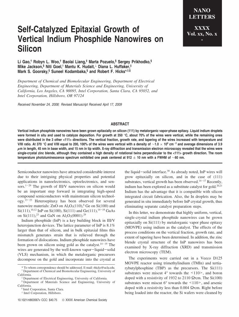
A top-view SEM image of InP nanowires deposited onSi(100) is shown in Figure 1a. The process conditions were370 °C and a V/III ratio of 200. The growth time was 25min. In the image, the nanowires appear bright, while thedarker grey contrast underneath them is due to a thin layerof interconnected InP islands. The density of the nanowiresis about 2.0 × 109 cm-2. The nanowires are tapered with atip diameter of 20 ( 3 nm and a base diameter of 30 ( 5nm. The length of the nanowires is 850 ( 50 nm. There arefour orientations of the wires with in-plane components at90° from each other. These correspond to the four <111>directions that can be extracted from the (100) crystal plane.As shown in Figure 1c, the four orientations form a 35.3°angle with the surface and are at 90° angles from each other.
These results indicate that the InP nanowires grow along the<111> directions, which is in agreement with earlierwork.14-19
A top-view SEM image of InP nanowires deposited onSi(111) is presented in Figure 1b. The process conditionswere 350 °C and a V/III ratio of 200. The growth time was6 min. The nanowires appear as three white lines each rotated120° from each other. Additional wires are orientatedperpendicular to the surface and appear as small bright spots.The density of the nanowires is about 4.6 × 109 cm-2. Thewires exhibit a uniform diameter of 45 ( 5 nm, and theirlength is 290 ( 100 nm. On the basis of Figure 1b, about69% of the as-grown nanowires are vertical. The orientationsseen in the image correspond to the four <111> directionsthat emerge from the (111) crystal plane; one is perpendicularto the surface, while the other three form a 19.5° angle withthe surface and a 120° angle with respect to each other, asshown in Figure 1c.
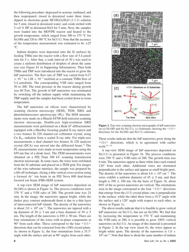
The above results indicate that it is feasible to grow verticalInP nanowires on Si(111), but not on Si(100). We find thatby increasing the temperature to 370 °C and maintainingthe V/III ratio at 200, it is possible to grow 100% verticalnanowires on Si(111). An image of this material is presentedin Figure 2. In the top view (inset b), the wires appear asbright white spots. The density of the nanowires is 1.0 ×109 cm-2. Note that there is about the same number of indium
Figure 1. Top view scanning electron micrographs of InP nanowireson (a) Si(100) and (b) Si(111). (c) Schematic showing the <111>directions for the Si(100) and Si(111) substrates.
B Nano Lett., Vol. xx, No. x, XXXX
droplet nucleation sites on the silicon surface. A similardensity of InP nanowires have been reported previously forgold catalysts on Si(111).14-18 Nevertheless, the length ofthe nanowires is 3.9 ( 0.2 µm, which is much longer thanthat has been seen before. The remainder of the paper willfocus on the results obtained with Si(111).
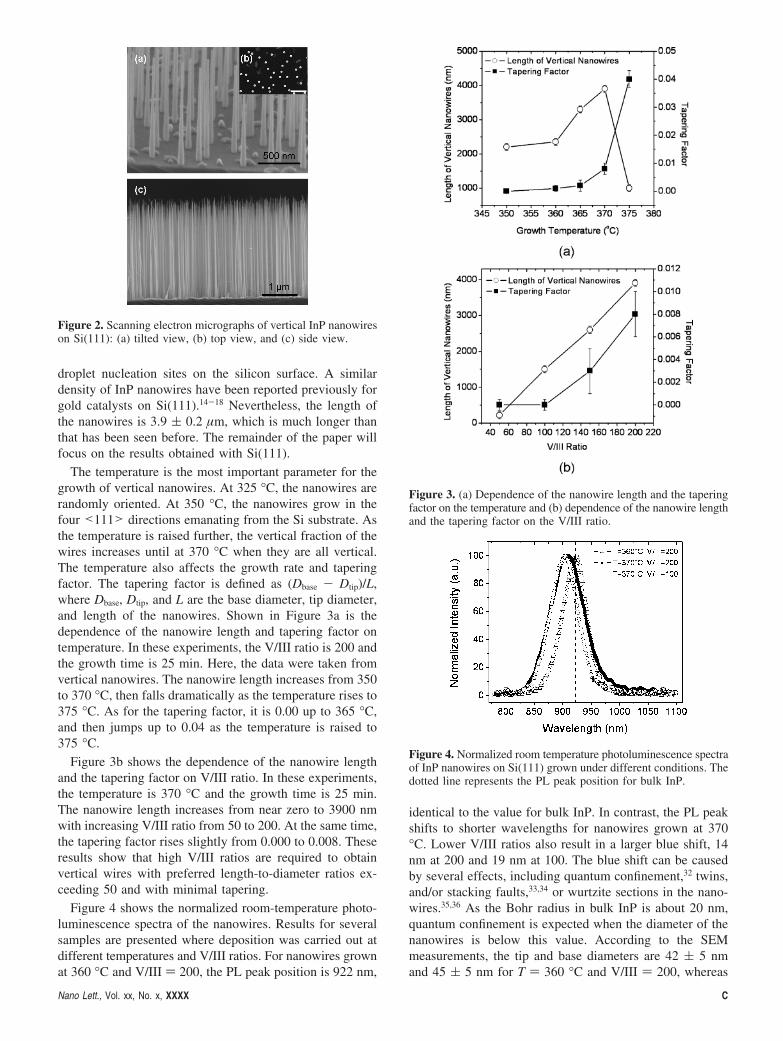
The temperature is the most important parameter for thegrowth of vertical nanowires. At 325 °C, the nanowires arerandomly oriented. At 350 °C, the nanowires grow in thefour <111> directions emanating from the Si substrate. Asthe temperature is raised further, the vertical fraction of thewires increases until at 370 °C when they are all vertical.The temperature also affects the growth rate and taperingfactor. The tapering factor is defined as (Dbase - Dtip)/L,where Dbase, Dtip, and L are the base diameter, tip diameter,and length of the nanowires. Shown in Figure 3a is thedependence of the nanowire length and tapering factor ontemperature. In these experiments, the V/III ratio is 200 andthe growth time is 25 min. Here, the data were taken fromvertical nanowires. The nanowire length increases from 350to 370 °C, then falls dramatically as the temperature rises to375 °C. As for the tapering factor, it is 0.00 up to 365 °C,and then jumps up to 0.04 as the temperature is raised to375 °C.
Figure 3b shows the dependence of the nanowire lengthand the tapering factor on V/III ratio. In these experiments,the temperature is 370 °C and the growth time is 25 min.The nanowire length increases from near zero to 3900 nmwith increasing V/III ratio from 50 to 200. At the same time,the tapering factor rises slightly from 0.000 to 0.008. Theseresults show that high V/III ratios are required to obtainvertical wires with preferred length-to-diameter ratios ex-ceeding 50 and with minimal tapering.
Figure 4 shows the normalized room-temperature photo-luminescence spectra of the nanowires. Results for severalsamples are presented where deposition was carried out atdifferent temperatures and V/III ratios. For nanowires grownat 360 °C and V/III ) 200, the PL peak position is 922 nm,
identical to the value for bulk InP. In contrast, the PL peakshifts to shorter wavelengths for nanowires grown at 370°C. Lower V/III ratios also result in a larger blue shift, 14nm at 200 and 19 nm at 100. The blue shift can be causedby several effects, including quantum confinement,32 twins,and/or stacking faults,33,34 or wurtzite sections in the nano-wires.35,36 As the Bohr radius in bulk InP is about 20 nm,quantum confinement is expected when the diameter of thenanowires is below this value. According to the SEMmeasurements, the tip and base diameters are 42 ( 5 nmand 45 ( 5 nm for T ) 360 °C and V/III ) 200, whereas
Figure 2. Scanning electron micrographs of vertical InP nanowireson Si(111): (a) tilted view, (b) top view, and (c) side view.
Figure 3. (a) Dependence of the nanowire length and the taperingfactor on the temperature and (b) dependence of the nanowire lengthand the tapering factor on the V/III ratio.
Figure 4. Normalized room temperature photoluminescence spectraof InP nanowires on Si(111) grown under different conditions. Thedotted line represents the PL peak position for bulk InP.
Nano Lett., Vol. xx, No. x, XXXX C
they are both 15 ( 2 nm for T ) 370 °C and V/III ) 100.The size effect seems to be the most likely explanation forthe blue shift, since none of the wires exhibit wurtzitedomains, while they all contain rotational twins.
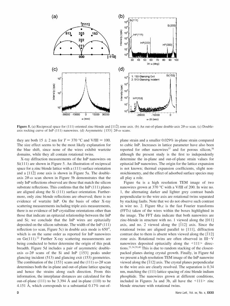
X-ray diffraction measurements of the InP nanowires onSi(111) are shown in Figure 5. An illustration of reciprocalspace for a zinc blende lattice with a (111) surface orientationand a [112j] zone axis is shown in Figure 5a. The double-axis 2θ-ω scan shown in Figure 5b demonstrates that theonly InP reflections observed are those that match the siliconsubstrate reflections. This confirms that the InP (111) planesare aligned along the Si (111) surface orientation. Further-more, only zinc blende reflections are observed; there is noevidence of wurtzite InP. On the basis of other X-rayscattering measurements including triple axis measurements,there is no evidence of InP crystalline orientations other thanthose that indicate an epitaxial relationship between the InPand Si; we conclude that the InP wires are epitaxiallydeposited on the silicon substrate. The width of the InP (111)reflection (ω scan, Figure 5c) in double axis mode is 650′′,which is on the same order as reported for InP nanowireson Ge(111).22 Further X-ray scattering measurements arebeing conducted to better determine the origin of this peakbreadth. Figure 5d includes a pair of asymmetric double-axis ω-2θ scans of the Si and InP 153 peaks underglancing incident (513) and glancing exit (153) geometries.The combination of the 153 scans and the (111) ω-2θ scandetermines both the in-plane and out-of-plane lattice spacingand hence the strains along each direction. From thisinformation, the interplanar distances are calculated for theout-of-plane (111) to be 3.394 Å and in-plane (110) to be4.151 Å, which corresponds to a substantial 0.17% out-of-
plane strain and a smaller 0.029% in-plane strain comparedto cubic InP. Increases in lattice parameter have also beenreported for other nanowires37 and for porous silicon,38
although the present study is the first to independentlydetermine the in-plane and out-of-plane strain values forepitaxial InP nanowires. The origin for the lattice expansionis not known; thermal expansion coefficients, slight non-stoichiometry, and the effect of adsorbed surface species mayall play a role.
Figure 6a is a high resolution TEM image of twonanowires grown at 370 °C with a V/III of 200. In wire no.1, the alternating darker and lighter grey contrast bandsperpendicular to the wire axis are rotational twins separatedby stacking faults. Note that we do not observe such contrastin wire no. 2. Figure 6b,c is the fast Fourier transforms(FFTs) taken of the wires within the boxes highlighted inthe image. The FFT data indicate that both nanowires arezinc-blende in structure with no. 1 viewed along the [011]axis, and no. 2 viewed along the [1j12] axis. Since therotational twins are aligned parallel to [111], diffractioncontrast due to them is absent when viewed along the [1j12]zone axis. Rotational twins are often observed in III-Vnanowires deposited epitaxially along the <111> direc-tions.21,34,39,40 This is due to random stacking of the closest-packed planes during crystal growth. Finally, in Figure 6dwe present a high resolution TEM image of the InP nanowireviewed along the [1j12] axis. The crystal planes perpendicularto the wire axis are clearly resolved. The separation is 0.34nm, matching the (111) lattice spacing of zinc blende indiumphosphide. The nanowires grown at different conditions,included in Figures 3a and 3b, all have the <111> zincblende structure with rotational twins.
Figure 5. (a) Reciprocal space for (111) oriented zinc-blende and [112j] zone axis. (b) An out-of-plane double-axis 2θ-ω scan. (c) Double-axis rocking curve of InP (111) nanowires. (d) Asymmetric 153 2θ-ω scans.
D Nano Lett., Vol. xx, No. x, XXXX
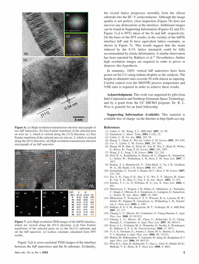
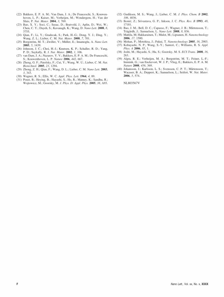
Figure 7a,b is cross-sectional TEM images of the interfacebetween the InP nanowires and the Si substrate. Evidently,
the crystal lattice progresses smoothly from the siliconsubstrate into the III-V semiconductor. Although the imagequality is not perfect, close inspection (Figure 7b) does notuncover any dislocations at the interface. Additional imagescan be found in Supporting Information (Figures S2 and S3).Figure 7c,d is FFTs taken of the Si and InP, respectively.On the basis of the FFT results, in the vicinity of the InP/Siinterface InP and Si have equivalent lattice constants, asshown in Figure 7e. This would suggest that the straininduced by the 8.1% lattice mismatch could be fullyaccommodated by elastic deformation. A similar observationhas been reported by Bakkers et al.15 Nevertheless, furtherhigh resolution images are required in order to prove ordisprove this hypothesis.
In summary, 100% vertical InP nanowires have beengrown on Si(111) using indium droplets as the catalysts. Theheight-to-diameter ratio exceeds 50 with almost no tapering.Careful control over the MOVPE process temperature andV/III ratio is required in order to achieve these results.
Acknowledgment. This work was supported by gifts fromIntel Corporation and Northrop Grumman Space Technology,and by a grant from the UC MICRO program. Dr. R. L.Woo is grateful for an Intel fellowship.
Supporting Information Available: This material isavailable free of charge via the Internet at http://pubs.acs.org.
References(1) Lieber, C. M.; Wang, Z. L. MRS Bull. 2007, 32, 99.(2) Samuelson, L. Mater. Today 2003, 6 (10), 22.(3) Lieber, C. M. Sci. Am. 2001, 285, 58.(4) Huang, Y.; Duan, X.; Wei, Q.; Lieber, C. M. Science 2001, 291, 630.(5) Cui, Y.; Lieber, C. M. Science 2001, 291, 851.(6) Huang, M. H.; Mao, S.; Feick, H.; Yan, H.; Wu, Y.; Kind, H.; Weber,
E.; Russo, R.; Yang, P. D. Science 2001, 292, 1897.(7) Wang, Z. L.; Song, J. H. Science 2006, 312, 242.(8) Dick, K. A.; Kodambaka, S.; Reuter, M. C.; Deppert, K.; Samuelson,
L.; Seifert, W.; Wallenberg, L. R.; Ross, F. M. Nano Lett. 2007, 7,1817.
(9) Boukai, A. I.; Bunimovich, Y.; Tahir-Kheli, J.; Yu, J.-K.; Goddard,W. A., III; Heath, J. R. Nature 2008, 451, 168.
(10) Kodambaka, S.; Tersoff, J.; Reuter, M. C.; Ross, F. M. Science 2007,316, 729.
(11) Xia, Y. N.; Yang, P. D.; Sun, Y. G.; Wu, Y. Y.; Mayers, B.; Gates,B.; Yin, Y. D.; Kim, F.; Yan, Y. Q. AdV. Mater. 2003, 15, 353.
(12) Kamins, T. I.; Li, X; Williams, R. S.; Liu, X. Nano Lett. 2004, 4,503.
(13) Mårtensson, T.; Wagner, J. B.; Hilner, E.; Mikkelsen, A.; Thelander,C.; Stangl, J.; Ohlsson, B. J.; Gustafsson, A.; Lundgren, E.; Samuelson,L.; Seifert, W. AdV. Mater. 2007, 19, 1801.
(14) Martensson, T.; Svensson, C. P. T.; Wacaser, B. A.; Larsson, M. W.;Seifert, W.; Deppert, K.; Gustafsson, A.; Wallenberg, L. R.; Samuel-son, L. Nano Lett. 2004, 4, 1987.
(15) Bakkers, E. P. A. M.; Borgstrom, M. T.; Verheijen, M. A. MRS Bull.2007, 32, 117.
(16) Chuang, L. C.; Moewe, M.; Crankshaw, S.; Chang-Hasnain, C. Appl.Phys. Lett. 2008, 92, 013121.
(17) Chuang, L. C.; Moewe, M.; Chase, C.; Kobayashi, N. P.; Chang-Hasnain, C.; Crankshaw, S. Appl. Phys. Lett. 2007, 90, 043115.
(18) Roest, A. L.; Verheijen, M. A.; Wunnicke, O.; Serafin, S.; Wondergem,H.; Bakkers, E. P. A. M. Nanotechnology 2006, 17, S271.
(19) Yi, S. S.; Girolami, G.; Amano, J.; Islam, M. S.; Sharma, S.; Kamins,T. I.; Kimukin, I. Appl. Phys. Lett. 2006, 89, 133121.
(20) Mattila, M.; Hakkarainen, T.; Lipsanen, H.; Jiang, H.; Kauppinen, E. I.Appl. Phys. Lett. 2006, 89, 063119.
(21) Woo, R. L.; Xiao, R.; Kobayashi, Y.; Gao, L.; Goel, N.; Hudait, M. K.;Mallouk, T. E.; Hicks, R. F. Nano Lett. 2008, 8, 4664.
Figure 6. (a) High resolution transmission electron micrograph oftwo InP nanowires. (b) Fast Fourier transform of the selected areaon wire no. 1, which is viewed along the [1j12] direction. (c) FastFourier transform of the selected area on wire no. 2, which is viewedalong the [011] direction. (d) High resolution transmission electronmicrograph of an InP nanowire.
Figure 7. (a,b) High-resolution TEM images of the InP/Si interface,which are viewed along the [011] direction. (c,d) Fast Fouriertransforms of the selected areas on (c) the Si(111) substrate and(d) the InP nanowire. (e) Lattice constants calculated from FFTresults.
Nano Lett., Vol. xx, No. x, XXXX E
(22) Bakkers, E. P. A. M.; Van Dam, J. A.; De Franceschi, S.; Kouwen-hoven, L. P.; Kaiser, M.; Verheijen, M.; Wondergem, H.; Van derSluis, P. Nat. Mater. 2004, 3, 769.
(23) Bao, X. Y.; Soci, C.; Susac, D.; Bratvold, J.; Aplin, D.; Wei, W.;Chen, C. Y.; Dayeh, S.; Kavanagh, K.; Wang, D. Nano Lett. 2008, 8,3755.
(24) Qian, F.; Li, Y.; Gradecak, S.; Park, H.-G.; Dong, Y. J.; Ding, Y.;Wang, Z. L.; Lieber, C. M. Nat. Mater. 2008, 7, 701.
(25) Borgstrom, M. T.; Zwiller, V.; Muller, E.; Imamoglu, A. Nano Lett.2005, 5, 1439.
(26) Johnson, J. C.; Choi, H.-J.; Knutsen, K. P.; Schaller, R. D.; Yang,P. D.; Saykally, R. J. Nat. Mater. 2002, 1, 106.
(27) van Dam, J. A.; Nazarov, Y. V.; Bakkers, E. P. A. M.; De Franceschi,S.; Kouwenhoven, L. P. Nature 2006, 442, 667.
(28) Zheng, G. F.; Patolsky, F.; Cui, Y.; Wang, W. U.; Lieber, C. M. Nat.Biotechnol. 2005, 23, 1294.
(29) Zhong, Z. H.; Qian, F.; Wang, D. L.; Lieber, C. M. Nano Lett. 2003,3, 343.
(30) Wagner, R. S.; Ellis, W. C. Appl. Phys. Lett. 1964, 4, 89.(31) Poust, B.; Heying, B.; Hayashi, S.; Ho, R.; Matney, K.; Sandhu, R.;
Wojtowicz, M.; Goorsky, M. J. Phys. D: Appl. Phys. 2005, 38, A93.
(32) Gudiksen, M. S.; Wang, J.; Lieber, C. M. J. Phys. Chem. B 2002,106, 4036.
(33) Ikonic, Z.; Srivastava, G. P.; Inkson, J. C. Phys. ReV. B 1993, 48,17181.
(34) Bao, J. M.; Bell, D. C.; Capasso, F.; Wagner, J. B.; Martensson, T.;Tragardh, J.; Samuelson, L. Nano Lett. 2008, 8, 836.
(35) Mattila, M; Hakkarainen, T.; Mulot, M.; Lipsanen, H. Nanotechnology2006, 17, 1580.
(36) Mohan, P.; Motohisa, J.; Fukui, T. Nanotechnology 2005, 16, 2903.(37) Kobayashi, N. P.; Wang, S.-Y.; Santori, C.; Williams, R. S. Appl.
Phys. A 2006, 85, 1.(38) Joshi, M.; Hayashi, S.; Hu, S.; Goorsky, M. S. ECS Trans. 2008, 16,
263.(39) Algra, R. E.; Verheijen, M. A.; Borgstrom, M. T.; Feiner, L.-F.;
Immink, G.; van Enckevort, W. J. P.; Vlieg, E.; Bakkers, E. P. A. M.Nature 2008, 456, 369.
(40) Johansson, J.; Karlsson, L. S.; Svensson, C. P. T.; Mårtensson, T.;Wacaser, B. A.; Deppert, K.; Samuelson, L.; Seifert, W. Nat. Mater.2006, 5, 574.
NL803567V
F Nano Lett., Vol. xx, No. x, XXXX
Related Documents


![Lattice matched epitaxial shell growth on InZnP quantum dots · A less toxic alternative for cadmium selenide quantum dots are indium phosphide quantum dots. [28] However, the PLQY,](https://static.cupdf.com/doc/110x72/5f0e4c8b7e708231d43e90ba/lattice-matched-epitaxial-shell-growth-on-inznp-quantum-dots-a-less-toxic-alternative.jpg)


