TLV702xx GND EN IN OUT V IN V OUT On Off C IN C OUT 1 F Ceramic m Product Folder Sample & Buy Technical Documents Tools & Software Support & Community TLV702 SLVSAG6C – SEPTEMBER 2010 – REVISED MARCH 2015 TLV702 300-mA, Low-I Q , Low-Dropout Regulator 1 Features 3 Description The TLV702 series of low-dropout (LDO) linear 1• Very Low Dropout: regulators are low quiescent current devices with – 37 mV at I OUT = 50 mA, V OUT = 2.8 V excellent line and load transient performance. These – 75 mV at I OUT = 100 mA, V OUT = 2.8 V LDOs are designed for power-sensitive applications. A precision bandgap and error amplifier provides – 220mV at I OUT = 300 mA, V OUT = 2.8 V overall 2% accuracy. Low output noise, very high • 2% Accuracy power-supply rejection ratio (PSRR), and low-dropout • Low I Q : 35 μA voltage make this series of devices ideal for a wide selection of battery-operated handheld equipment. All • Fixed-Output Voltage Combinations Possible from device versions have thermal shutdown and current 1.2 V to 4.8 V limit for safety. • High PSRR: 68 dB at 1 kHz Furthermore, these devices are stable with an • Stable With Effective Capacitance of 0.1 μF (1) effective output capacitance of only 0.1 μF. This • Thermal Shutdown and Overcurrent Protection feature enables the use of cost-effective capacitors • Packages: 5-Pin SOT-23 and 1.5-mm × 1.5-mm, that have higher bias voltages and temperature 6-Pin WSON derating. The devices regulate to specified accuracy with no output load. (1) See the Input and Output Capacitor Requirements in Application Information. The TLV702P series also provides an active pulldown circuit to quickly discharge the outputs. 2 Applications The TLV702 series of LDO linear regulators are • Wireless Handsets available in SOT23-5 and 1.5-mm × 1.5-mm SON-6 • Smart Phones packages. • ZigBee ® Networks Device Information (1) • Bluetooth ® Devices PART NUMBER PACKAGE BODY SIZE (NOM) • Li-Ion Battery-Operated Handheld Products SOT-23 (5) 2.90 mm × 1.60 mm TLV702 • WLAN and Other PC Add-on Cards WSON (6) 1.50 mm × 1.50 mm (1) For all available packages, see the orderable addendum at the end of the data sheet. Typical Application Circuit 1 An IMPORTANT NOTICE at the end of this data sheet addresses availability, warranty, changes, use in safety-critical applications, intellectual property matters and other important disclaimers. PRODUCTION DATA.

Welcome message from author
This document is posted to help you gain knowledge. Please leave a comment to let me know what you think about it! Share it to your friends and learn new things together.
Transcript

TLV702xx
GND
EN
IN OUTVIN
VOUT
On
Off
CIN
COUT
1 F
Ceramic
m
Product
Folder
Sample &Buy
Technical
Documents
Tools &
Software
Support &Community
TLV702SLVSAG6C –SEPTEMBER 2010–REVISED MARCH 2015
TLV702 300-mA, Low-IQ, Low-Dropout Regulator1 Features 3 Description
The TLV702 series of low-dropout (LDO) linear1• Very Low Dropout:
regulators are low quiescent current devices with– 37 mV at IOUT = 50 mA, VOUT = 2.8 V excellent line and load transient performance. These– 75 mV at IOUT = 100 mA, VOUT = 2.8 V LDOs are designed for power-sensitive applications.
A precision bandgap and error amplifier provides– 220mV at IOUT = 300 mA, VOUT = 2.8 Voverall 2% accuracy. Low output noise, very high• 2% Accuracy power-supply rejection ratio (PSRR), and low-dropout
• Low IQ: 35 μA voltage make this series of devices ideal for a wideselection of battery-operated handheld equipment. All• Fixed-Output Voltage Combinations Possible fromdevice versions have thermal shutdown and current1.2 V to 4.8 Vlimit for safety.• High PSRR: 68 dB at 1 kHzFurthermore, these devices are stable with an• Stable With Effective Capacitance of 0.1 μF(1)
effective output capacitance of only 0.1 μF. This• Thermal Shutdown and Overcurrent Protection feature enables the use of cost-effective capacitors• Packages: 5-Pin SOT-23 and 1.5-mm × 1.5-mm, that have higher bias voltages and temperature
6-Pin WSON derating. The devices regulate to specified accuracywith no output load.(1) See the Input and Output Capacitor Requirements in
Application Information. The TLV702P series also provides an active pulldowncircuit to quickly discharge the outputs.2 ApplicationsThe TLV702 series of LDO linear regulators are
• Wireless Handsets available in SOT23-5 and 1.5-mm × 1.5-mm SON-6• Smart Phones packages.• ZigBee® Networks
Device Information(1)• Bluetooth® Devices
PART NUMBER PACKAGE BODY SIZE (NOM)• Li-Ion Battery-Operated Handheld Products
SOT-23 (5) 2.90 mm × 1.60 mmTLV702• WLAN and Other PC Add-on Cards
WSON (6) 1.50 mm × 1.50 mm
(1) For all available packages, see the orderable addendum atthe end of the data sheet.
Typical Application Circuit
1
An IMPORTANT NOTICE at the end of this data sheet addresses availability, warranty, changes, use in safety-critical applications,intellectual property matters and other important disclaimers. PRODUCTION DATA.

TLV702SLVSAG6C –SEPTEMBER 2010–REVISED MARCH 2015 www.ti.com
Table of Contents8.1 Application Information............................................ 131 Features .................................................................. 18.2 Typical Application .................................................. 132 Applications ........................................................... 1
9 Power Supply Recommendations ...................... 153 Description ............................................................. 19.1 Power Dissipation ................................................... 154 Revision History..................................................... 2
10 Layout................................................................... 155 Pin Configuration and Functions ......................... 310.1 Layout Guidelines ................................................. 156 Specifications......................................................... 410.2 Layout Examples................................................... 156.1 Absolute Maximum Ratings ...................................... 410.3 Thermal Consideration.......................................... 166.2 ESD Ratings ............................................................ 410.4 Package Mounting ................................................ 166.3 Recommended Operating Conditions....................... 4
11 Device and Documentation Support ................. 176.4 Thermal Information .................................................. 411.1 Device Support .................................................... 176.5 Electrical Characteristics........................................... 511.2 Documentation Support ........................................ 176.6 Typical Characteristics .............................................. 611.3 Related Links ........................................................ 177 Detailed Description ............................................ 1011.4 Trademarks ........................................................... 187.1 Overview ................................................................. 1011.5 Electrostatic Discharge Caution............................ 187.2 Functional Block Diagrams ..................................... 1011.6 Glossary ................................................................ 187.3 Feature Description................................................. 11
12 Mechanical, Packaging, and Orderable7.4 Device Functional Modes........................................ 12Information ........................................................... 188 Application and Implementation ........................ 13
4 Revision HistoryNOTE: Page numbers for previous revisions may differ from page numbers in the current version.
Changes from Revision B (February 2011) to Revision C Page
• Added ESD Ratings table, Feature Description section, Device Functional Modes, Application and Implementationsection, Power Supply Recommendations section, Layout section, Device and Documentation Support section, andMechanical, Packaging, and Orderable Information section ................................................................................................. 1
• Changed Pin Configuration and Functions section; updated table format ............................................................................ 3• Deleted Ordering Information table ....................................................................................................................................... 3• Changed "free-air temperature" to "junction temperature" in Absolute Maximum Ratings condition statement ................... 4• Changed Thermal Information table; updated thermal resistance values for all packages .................................................. 4• Deleted Dissipation Ratings table .......................................................................................................................................... 4• Changed VDO dropout voltage test conditions; deleted IOUT = 50 mA and IOUT = 100 mA with VOUT = 2.8 V test
parameters ............................................................................................................................................................................. 5• Deleted EVM Dissipation Ratings table ............................................................................................................................... 16
Changes from Revision A (October 2010) to Revision B Page
• Added SON-6 (DSE) package and related references to data sheet..................................................................................... 1
2 Submit Documentation Feedback Copyright © 2010–2015, Texas Instruments Incorporated
Product Folder Links: TLV702

OUT
NC
IN
GND
EN
1
2
3
5
4
EN
N/C
N/C
6
5
4
IN
GND
OUT
1
2
3
TLV702www.ti.com SLVSAG6C –SEPTEMBER 2010–REVISED MARCH 2015
5 Pin Configuration and Functions
DBV PackageDSE Package5-Pin SOT-236-Pin WSONTop View
Top View
Pin FunctionsPIN
I/O DESCRIPTIONNAME SOT-23 WSON
Input pin. A small, 1-μF ceramic capacitor is recommended from this pin to ground toIN 1 1 I assure stability and good transient performance. See Input and Output Capacitor
Requirements in Application Information for more details.GND 2 2 — Ground pin
Enable pin. Driving EN over 0.9 V turns on the regulator. Driving EN below 0.4 V putsthe regulator into shutdown mode and reduces operating current to 1 μA, nominal.EN 3 6 I For TLV702P, output voltage is discharged through an internal 120-Ω resistor whendevice is shut down.
NC 4 4, 5 — No connection. This pin can be tied to ground to improve thermal dissipation.Regulated output voltage pin. A small, 1-μF ceramic capacitor is needed from this pin
OUT 5 5 O to ground to assure stability. See Input and Output Capacitor Requirements inApplication Information for more details.
Copyright © 2010–2015, Texas Instruments Incorporated Submit Documentation Feedback 3
Product Folder Links: TLV702

TLV702SLVSAG6C –SEPTEMBER 2010–REVISED MARCH 2015 www.ti.com
6 Specifications
6.1 Absolute Maximum Ratingsover operating junction temperature range (unless otherwise noted) (1)
MIN MAX UNITIN –0.3 6
Voltage (2) EN –0.3 6 VOUT –0.3 6
Current (source) OUT Internally limitedOutput short-circuit duration IndefiniteTotal continuous power dissipation See Thermal Information
Operating virtual junction, TJ –55 150Temperature °C
Storage, Tstg –55 150
(1) Stresses beyond those listed under Absolute Maximum Ratings may cause permanent damage to the device. These are stress ratingsonly, and functional operation of the device at these or any other conditions beyond those indicated under Recommended OperatingConditions is not implied. Exposure to absolute-maximum-rated conditions for extended periods my affect device reliability.
(2) All voltages are with respect to network ground terminal.
6.2 ESD RatingsVALUE UNIT
Human body model (HBM), per ANSI/ESDA/JEDEC JS-001, all pins (1) ±2000V(ESD) Electrostatic discharge VCharged device model (CDM), per JEDEC specification JESD22-C101, ±500all pins (2)
(1) JEDEC document JEP155 states that 500-V HBM allows safe manufacturing with a standard ESD control process.(2) JEDEC document JEP157 states that 250-V CDM allows safe manufacturing with a standard ESD control process.
6.3 Recommended Operating Conditionsover operating free-air temperature range (unless otherwise noted).
MIN NOM MAX UNITVIN 2 5.5 VVOUT 1.2 4.8 VIOUT 0 300 mA
6.4 Thermal InformationTLV702
THERMAL METRIC (1) DBV (SOT-23) DSE (WSON) UNIT5 PINS 6 PINS
RθJA Junction-to-ambient thermal resistance 249.2 321.3RθJC(top) Junction-to-case (top) thermal resistance 136.4 207.9RθJB Junction-to-board thermal resistance 85.9 281.5
°C/WψJT Junction-to-top characterization parameter 19.5 42.4ψJB Junction-to-board characterization parameter 85.3 284.8RθJC(bot) Junction-to-case (bottom) thermal resistance N/A 142.3
(1) For more information about traditional and new thermal metrics, see the IC Package Thermal Metrics application report, SPRA953.
4 Submit Documentation Feedback Copyright © 2010–2015, Texas Instruments Incorporated
Product Folder Links: TLV702

TLV702www.ti.com SLVSAG6C –SEPTEMBER 2010–REVISED MARCH 2015
6.5 Electrical CharacteristicsAt VIN = VOUT(nom) + 0.5 V or 2 V (whichever is greater); IOUT = 10 mA, VEN = 0.9 V, COUT = 1 μF, and TJ = –40°C to +125°C,unless otherwise noted. Typical values are at TJ = 25°C.
PARAMETER TEST CONDITIONS MIN TYP MAX UNITVIN Input voltage range 2 5.5 VVOUT DC output accuracy –40°C ≤ TJ ≤ 125°C –2% 0.5% 2%
VOUT(nom) + 0.5 V ≤ VIN ≤ 5.5 V,ΔVOUT(ΔVIN) Line regulation 1 5 mVIOUT = 10 mAΔVOUT(ΔIOUT) Load regulation 0 mA ≤ IOUT ≤ 300 mA 1 15 mVVDO Dropout voltage (1) VIN = 0.98 × VOUT(nom), IOUT = 300 mA 260 375 mVICL Output current limit VOUT = 0.9 × VOUT(nom) 320 500 860 mA
IOUT = 0 mA 35 55 μAIGND Ground pin current
IOUT = 300 mA, VIN = VOUT + 0.5 V 370 μAVEN ≤ 0.4 V, VIN = 2 V 400 nA
ISHDN Ground pin current (shutdown) VEN ≤ 0.4 V, 2 V ≤ VIN ≤ 4.5 V, 1 2 μATJ = –40°C to +85°CVIN = 2.3 V, VOUT = 1.8 V,PSRR Power-supply rejection ratio 68 dBIOUT = 10 mA, f = 1 kHzBW = 100 Hz to 100 kHz,Vn Output noise voltage 48 μVRMSVIN = 2.3 V, VOUT = 1.8 V, IOUT = 10 mA
tSTR Start-up time (2) COUT = 1 μF, IOUT = 300 mA 100 μsVEN(high) Enable pin high (enabled) 0.9 VIN VVEN(low) Enable pin low (disabled) 0 0.4 VIEN Enable pin current VIN = VEN = 5.5 V 0.04 μAUVLO Undervoltage lockout VIN rising 1.9 V
Active pulldown resistanceRDISCHARGE VEN = 0 V 120 Ω(TLV702P only)Shutdown, temperature increasing 165 °C
Tsd Thermal shutdown temperatureReset, temperature decreasing 145 °C
TJ Operating junction temperature –40 125 °C
(1) VDO is measured for devices with VOUT(nom) ≥ 2.35 V.(2) Start-up time = time from EN assertion to 0.98 × VOUT(nom).
Copyright © 2010–2015, Texas Instruments Incorporated Submit Documentation Feedback 5
Product Folder Links: TLV702
0 100 150 300
I (mA)OUT
300
250
200
150
100
50
0
V(m
V)
DO
50 200
+125 C°
+85 C°
+25 C°
-40 C°
V = 4.8 VOUT
250
1.90
1.88
1.86
1.84
1.82
1.80
1.78
1.76
1.74
1.72
1.70
V(V
)O
UT
-40 -25 -10 5 20 35 50 65 80 95 110
Temperature ( C)°
125
10mA
150mA
200mA
V = 1.8 VOUT
0 100 150 300
I (mA)OUT
1.90
1.88
1.86
1.84
1.82
1.80
1.78
1.76
1.74
1.72
1.70
V(V
)O
UT
50 200
+125 C°
+85 C°
+25 C°
-40 C°
V = 1.8 VOUT
250
350
300
250
200
150
100
50
0
V(m
V)
DO
2.25 2.75 3.25 3.75 4.25 4.75
V (V)IN
+125 C°
+85 C°
+25 C°
-40 C°
I = 300mAOUT
1.90
1.88
1.86
1.84
1.82
1.80
1.78
1.76
1.74
1.72
1.70
VO
UT
(V)
2.1 2.6 3.1 3.6 4.1 4.6 5.1
V (V)IN
5.6
+125 C°
+85 C°
+25 C°
-40 C°
V = 1.8 V
I = 10 mAOUT
OUT
1.90
1.88
1.86
1.84
1.82
1.80
1.78
1.76
1.74
1.72
1.70
VO
UT
(V)
2.3 2.7 3.1 3.5 3.9 4.3 4.7
V (V)IN
5.55.1
+125 C°
+85 C°
+25 C°
-40 C°
V = 1.8 V
I = 300 mAOUT
OUT
TLV702SLVSAG6C –SEPTEMBER 2010–REVISED MARCH 2015 www.ti.com
6.6 Typical CharacteristicsOver operating temperature range (TJ = –40°C to +125°C), VIN = VOUT(nom) + 0.5 V or 2 V, whichever is greater; IOUT = 10 mA,VEN = VIN, COUT = 1 μF, unless otherwise noted. Typical values are at TJ = 25°C.
Figure 1. Line Regulation Figure 2. Line Regulation
Figure 3. Load Regulation Figure 4. Dropout Voltage vs Input Voltage
Figure 6. Output Voltage vs TemperatureFigure 5. Dropout Voltage vs Output Current
6 Submit Documentation Feedback Copyright © 2010–2015, Texas Instruments Incorporated
Product Folder Links: TLV702

100
90
80
70
60
50
40
30
20
10
0
PS
RR
(d
B)
10 100 1 k 10 k 100 k 1 M 10 M
Frequency (Hz)
I = 150 mAOUT
I = 10 mAOUT
V V = 0.5 VIN OUT-
700
600
500
400
300
200
100
0
I LIM
(mA
)
2.3 2.7 3.1 3.5 3.9 4.3 4.7
V (V)IN
5.55.1
V = 1.8 VOUT
+125 C°
+85 C°
+25 C°
-40 C°
50
45
40
35
30
25
20
15
10
5
0
I(
A)
mG
ND
-40 -25 -10 5 20 35 50 65 80 95 110
Temperature ( C)°
125
V = 1.8 VOUT
2.5
2
1.5
1
0.5
0
I SH
DN
(A
m)
2.1 2.6 3.1 3.6 4.1 4.6 5.1
V (V)IN
5.6
+125 C°
+85 C°
+25 C°
-40 C°
V = 1.8 VOUT
50
45
40
35
30
25
20
15
10
5
0
I GN
D(
Am
)
2.1 2.6 3.1 3.6 4.1 4.6 5.1
V (V)IN
5.6
+125 C°
+85 C°
+25 C°
-40 C°
V = 1.8 VOUT
450
400
350
300
250
200
150
100
50
0
I GN
D(m
A)
0
I (mA)OUT
300
+125 C°
+85 C°
+25 C°
-40 C°
V = 1.8 VOUT
50 150 250100 200
TLV702www.ti.com SLVSAG6C –SEPTEMBER 2010–REVISED MARCH 2015
Typical Characteristics (continued)Over operating temperature range (TJ = –40°C to +125°C), VIN = VOUT(nom) + 0.5 V or 2 V, whichever is greater; IOUT = 10 mA,VEN = VIN, COUT = 1 μF, unless otherwise noted. Typical values are at TJ = 25°C.
Figure 7. Ground Pin Current vs Input Voltage Figure 8. Ground Pin Current vs Load
Figure 9. Ground Pin Current vs Temperature Figure 10. Shutdown Current vs Input Voltage
Figure 11. Current Limit vs Input Voltage Figure 12. Power-Supply Ripple Rejection vs Frequency
Copyright © 2010–2015, Texas Instruments Incorporated Submit Documentation Feedback 7
Product Folder Links: TLV702

50
mA
/div
20
mV
/div
10 s/divm
VOUT
IOUT 50 mA
0 mA
t = t = 1 sR F m
VOUT = 1.8 V
20
0 m
A/d
iv1
00
mV
/div
10 s/divm
VOUT
300mA
0 mA
t =t = sR F m1
IOUT
VOUT = 1.8 V
10
0 m
A/d
iv5
0 m
V/d
iv
10 s/divm
VOUT
IOUT
200 mA
0 mA
t = t = 1 sR F m
VOUT = 1.8 V
20
mA
/div
5 m
V/d
iv
10 s/divm
VOUT
VOUT = 1.8 V
IOUT
10 mA
0 mA
t = t = 1 sR F m
2.1 2.2 2.3 2.4 2.5 2.6 2.7 2.8
Input Voltage (V)
80
70
60
50
40
30
20
10
0
PS
RR
(d
B)
10 kHz
100 kHz
1 kHz V = 1.8 VOUT
10
1
0.1
0.01
0.001
Ou
tpu
t S
pe
ctr
al N
ois
e D
en
sity (
V/
)m
ÖH
z
10 100 1 k 10 k 100 k 1 M 10 M
Frequency (Hz)
V = 1.8 VOUT
I = 10 mA
C = C = 1 FOUT
IN OUT m
TLV702SLVSAG6C –SEPTEMBER 2010–REVISED MARCH 2015 www.ti.com
Typical Characteristics (continued)Over operating temperature range (TJ = –40°C to +125°C), VIN = VOUT(nom) + 0.5 V or 2 V, whichever is greater; IOUT = 10 mA,VEN = VIN, COUT = 1 μF, unless otherwise noted. Typical values are at TJ = 25°C.
Figure 14. Output Spectral Noise Density vs FrequencyFigure 13. Power-Supply Ripple Rejection vs Input Voltage
Figure 15. Load Transient Response Figure 16. Load Transient Response
Figure 17. Load Transient Response Figure 18. Load Transient Response
8 Submit Documentation Feedback Copyright © 2010–2015, Texas Instruments Incorporated
Product Folder Links: TLV702

1 V
/div
10
mV
/div
1 ms/div
Slew Rate = 1 V/ sm
V = 1.8 V
I = 300 mA
OUT
OUT5.5 V
VIN2.1 V
VOUT
1 V
/div
200 ms/div
VOUT
VIN
V = 1.8 VOUT
I 1 mAOUT =
1 V
/div
5 m
V/d
iv
1 ms/div
VOUT
Slew Rate = 1 V/ sm
VIN
2.9 V
2.3 V
V = 1.8 V
I 300 mA
OUT
OUT =
1 V
/div
5 m
V/d
iv
1 ms/div
VOUT
VIN 2.9 V
2.3 V
V = 1.8 V
I 1 mA
OUT
OUT =
Slew Rate = 1 V/ sm
TLV702www.ti.com SLVSAG6C –SEPTEMBER 2010–REVISED MARCH 2015
Typical Characteristics (continued)Over operating temperature range (TJ = –40°C to +125°C), VIN = VOUT(nom) + 0.5 V or 2 V, whichever is greater; IOUT = 10 mA,VEN = VIN, COUT = 1 μF, unless otherwise noted. Typical values are at TJ = 25°C.
Figure 19. Line Transient Response Figure 20. Line Transient Response
Figure 21. Line Transient Response Figure 22. VIN Ramp Up, Ramp Down Response
Copyright © 2010–2015, Texas Instruments Incorporated Submit Documentation Feedback 9
Product Folder Links: TLV702

ThermalShutdown
CurrentLimit
UVLO
Bandgap
IN
EN
OUT
LOGIC
GND
TLV702xx Series
TLV702SLVSAG6C –SEPTEMBER 2010–REVISED MARCH 2015 www.ti.com
7 Detailed Description
7.1 OverviewThe TLV702 series of low-dropout (LDO) linear regulators are low quiescent current devices with excellent lineand load transient performance. These LDOs are designed for power-sensitive applications. A precision bandgapand error amplifier provides overall 2% accuracy. Low output noise, very high power-supply rejection ratio(PSRR), and low dropout voltage make this series of devices ideal for most battery-operated handheldequipment. All device versions have integrated thermal shutdown, current limit, and undervoltage lockout(UVLO).
7.2 Functional Block Diagrams
Figure 23. TLV702 Block Diagram
10 Submit Documentation Feedback Copyright © 2010–2015, Texas Instruments Incorporated
Product Folder Links: TLV702

t =(120 R )
(120 + R )L
L
·
· COUT
ThermalShutdown
CurrentLimit
UVLO
Bandgap
IN
EN
OUT
LOGIC
GND
TLV702xxP Series
120W
TLV702www.ti.com SLVSAG6C –SEPTEMBER 2010–REVISED MARCH 2015
Functional Block Diagrams (continued)
Figure 24. TLV702P Block Diagram
7.3 Feature Description
7.3.1 Internal Current LimitThe TLV702 internal current limit helps to protect the regulator during fault conditions. During current limit, theoutput sources a fixed amount of current that is largely independent of the output voltage. In such a case, theoutput voltage is not regulated, and is VOUT = ICL × RLOAD. The PMOS pass transistor dissipates (VIN – VOUT) ×ICL until thermal shutdown is triggered and the device turns off. As the device cools, it is turned on by the internalthermal shutdown circuit. If the fault condition continues, the device cycles between current limit and thermalshutdown. See Thermal Consideration for more details.
The PMOS pass element in the TLV702 has a built-in body diode that conducts current when the voltage at OUTexceeds the voltage at IN. This current is not limited, so if extended reverse voltage operation is anticipated,external limiting to 5% of the rated output current is recommended.
7.3.2 ShutdownThe enable pin (EN) is active high. The device is enabled when voltage at EN pin goes above 0.9 V. The deviceis turned off when the EN pin is held at less than 0.4 V. When shutdown capability is not required, EN can beconnected to the IN pin.
The TLV702P version has internal active pulldown circuitry that discharges the output with a time constant of:
where:• RL = Load resistance• COUT = Output capacitor (1)
Copyright © 2010–2015, Texas Instruments Incorporated Submit Documentation Feedback 11
Product Folder Links: TLV702
TLV702SLVSAG6C –SEPTEMBER 2010–REVISED MARCH 2015 www.ti.com
Feature Description (continued)7.3.3 Dropout VoltageThe TLV702 uses a PMOS pass transistor to achieve low dropout. When (VIN – VOUT) is less than the dropoutvoltage (VDO), the PMOS pass device is in the linear (triode) region of operation and the input-to-outputresistance is the RDS(on) of the PMOS pass element. VDO scales approximately with output current because thePMOS device behaves as a resistor in dropout.
As with any linear regulator, PSRR and transient response are degraded as (VIN – VOUT) approaches dropout.This effect is shown in Figure 13.
7.3.4 Undervoltage LockoutThe TLV702 uses a UVLO circuit to keep the output shut off until internal circuitry is operating properly.
7.4 Device Functional Modes
7.4.1 Normal OperationThe device regulates to the nominal output voltage under the following conditions:
• The input voltage is greater than the nominal output voltage added to the dropout voltage.• The output current is less than the current limit.• The input voltage is greater than the UVLO voltage.
7.4.2 Dropout OperationIf the input voltage is lower than the nominal output voltage plus the specified dropout voltage, but all otherconditions are met for normal operation, the device operates in dropout mode. In this condition, the outputvoltage is the same as the input voltage minus the dropout voltage. The transient performance of the device issignificantly degraded because the pass device is in a triode state and no longer regulates the output voltage ofthe LDO. Line or load transients in dropout may result in large output voltage deviations.
Table 1 lists the conditions that lead to the different modes of operation.
Table 1. Device Functional Mode ComparisonPARAMETER
OPERATING MODEVIN IOUT
Normal mode VIN > VOUT (nom) + VDO IOUT < ICL
Dropout mode VIN < VOUT (nom) + VDO IOUT < ICL
Current limit VIN > UVLO IOUT > ICL
12 Submit Documentation Feedback Copyright © 2010–2015, Texas Instruments Incorporated
Product Folder Links: TLV702

TLV702xx
GND
EN
IN OUTVIN
VOUT
On
Off
CIN
COUT
1 F
Ceramic
m
TLV702www.ti.com SLVSAG6C –SEPTEMBER 2010–REVISED MARCH 2015
8 Application and Implementation
NOTEInformation in the following applications sections is not part of the TI componentspecification, and TI does not warrant its accuracy or completeness. TI’s customers areresponsible for determining suitability of components for their purposes. Customers shouldvalidate and test their design implementation to confirm system functionality.
8.1 Application InformationThe TLV702 belongs to a new family of next-generation value LDO regulators. These devices consume lowquiescent current and deliver excellent line and load transient performance. These characteristics, combined withlow noise and very good PSRR with little (VIN – VOUT) headroom, make this family of devices ideal for portableRF applications. This family of regulators offers current limit and thermal protection, and is specified from –40°Cto +125°C.
8.2 Typical Application
Figure 25. Typical Application Circuit
8.2.1 Design RequirementsTable 2 lists the design parameters.
Table 2. Design ParametersPARAMETER DESIGN REQUIREMENTInput voltage 2.5 V to 3.3 V
Output voltage 1.8 VOutput current 100 mA
8.2.2 Detailed Design Procedure
8.2.2.1 Input and Output Capacitor Requirements1-μF X5R- and X7R-type ceramic capacitors are recommended because these capacitors have minimal variationin value and equivalent series resistance (ESR) overtemperature.
However, the TLV702 is designed to be stable with an effective capacitance of 0.1 μF or larger at the output.Thus, the device is stable with capacitors of other dielectric types as well, as long as the effective capacitanceunder operating bias voltage and temperature is greater than 0.1 μF. This effective capacitance refers to thecapacitance that the LDO sees under operating bias voltage and temperature conditions; that is, the capacitanceafter taking both bias voltage and temperature derating into consideration. In addition to allowing the use oflower-cost dielectrics, this capability of being stable with 0.1-μF effective capacitance also enables the use ofsmaller footprint capacitors that have higher derating in size- and space-constrained applications.
Using a 0.1-μF rated capacitor at the output of the LDO does not ensure stability because the effectivecapacitance under the specified operating conditions must not be less than 0.1 μF. Maximum ESR should beless than 200 mΩ.
Copyright © 2010–2015, Texas Instruments Incorporated Submit Documentation Feedback 13
Product Folder Links: TLV702

1 V
/div
5 m
V/d
iv
1 ms/div
VOUT
VIN 2.9 V
2.3 V
V = 1.8 V
I 1 mA
OUT
OUT =
Slew Rate = 1 V/ sm
50
mA
/div
20
mV
/div
10 s/divm
VOUT
IOUT 50 mA
0 mA
t = t = 1 sR F m
VOUT = 1.8 V
TLV702SLVSAG6C –SEPTEMBER 2010–REVISED MARCH 2015 www.ti.com
Although an input capacitor is not required for stability, it is good analog design practice to connect a 0.1-μF to 1-μF, low ESR capacitor across the IN pin and GND pin of the regulator. This capacitor counteracts reactive inputsources and improves transient response, noise rejection, and ripple rejection. A higher-value capacitor may benecessary if large, fast rise-time load transients are anticipated, or if the device is not located close to the powersource. If source impedance is more than 2 Ω, a 0.1-μF input capacitor may be necessary to ensure stability.
8.2.2.2 Transient ResponseAs with any regulator, increasing the size of the output capacitor reduces overshoot and undershoot magnitudebut increases the duration of the transient response.
8.2.3 Application Curves
Figure 26. Load Transient Response Figure 27. Line Transient Response
14 Submit Documentation Feedback Copyright © 2010–2015, Texas Instruments Incorporated
Product Folder Links: TLV702

COUT
VOUTVIN
GND PLANE
CIN
Represents via used for application specific connections
IN
GND
EN NC
OUT
P = (V V ) I- ´D IN OUT OUT
TLV702www.ti.com SLVSAG6C –SEPTEMBER 2010–REVISED MARCH 2015
9 Power Supply RecommendationsConnect a low output impedance power supply directly to the INPUT pin of the TLV702. Inductive impedancesbetween the input supply and the INPUT pin can create significant voltage excursions at the INPUT pin duringstart-up or load transient events.
9.1 Power DissipationThe ability to remove heat from the die is different for each package type, presenting different considerations inthe printed-circuit-board (PCB) layout. The PCB area around the device that is free of other components movesthe heat from the device to the ambient air.
Refer to Thermal Information for thermal performance on the TLV702 evaluation module (EVM). The EVM is atwo-layer board with two ounces of copper per side.
Power dissipation depends on input voltage and load conditions. Power dissipation (PD) is equal to the product ofthe output current and the voltage drop across the output pass element, as shown in Equation 2.
(2)
10 Layout
10.1 Layout GuidelinesInput and output capacitors should be placed as close to the device pins as possible. To improve ACperformance such as PSRR, output noise, and transient response, TI recommends designing the board withseparate ground planes for VIN and VOUT, with the ground plane connected only at the GND pin of the device. Inaddition, the ground connection for the output capacitor should be connected directly to the GND pin of thedevice. High ESR capacitors may degrade PSRR performance.
10.2 Layout Examples
Figure 28. Layout Example for the DBV Package
Copyright © 2010–2015, Texas Instruments Incorporated Submit Documentation Feedback 15
Product Folder Links: TLV702

COUTVOUT
VIN
GND PLANE
CIN
Represents via used for application specific connections
IN
GND
OUT NC
EN
NC
TLV702SLVSAG6C –SEPTEMBER 2010–REVISED MARCH 2015 www.ti.com
Layout Examples (continued)
Figure 29. Layout Example for the DSE Package
10.3 Thermal ConsiderationThermal protection disables the output when the junction temperature rises to approximately 165°C, allowing thedevice to cool. When the junction temperature cools to approximately 145°C, the output circuitry is againenabled. Depending on power dissipation, thermal resistance, and ambient temperature, the thermal protectioncircuit may cycle on and off. This cycling limits the dissipation of the regulator, protecting it from damage as aresult of overheating.
Any tendency to activate the thermal protection circuit indicates excessive power dissipation or an inadequateheatsink. For reliable operation, junction temperature should be limited to 125°C maximum.
To estimate the margin of safety in a complete design (including heatsink), increase the ambient temperatureuntil the thermal protection is triggered; use worst-case loads and signal conditions.
The internal protection circuitry of the TLV702 has been designed to protect against overload conditions. It wasnot intended to replace proper heatsinking. Continuously running the TLV702 into thermal shutdown degradesdevice reliability.
10.4 Package MountingSolder pad footprint recommendations for the TLV702 are available from the TI website at www.ti.com. Therecommended land pattern for the DBV and DSE packages are shown in Figure 28 and Figure 29, respectively.
16 Submit Documentation Feedback Copyright © 2010–2015, Texas Instruments Incorporated
Product Folder Links: TLV702

TLV702www.ti.com SLVSAG6C –SEPTEMBER 2010–REVISED MARCH 2015
11 Device and Documentation Support
11.1 Device Support
11.1.1 Development Support
11.1.1.1 Spice ModelsComputer simulation of circuit performance using SPICE is often useful when analyzing the performance ofanalog circuits and systems. A SPICE model for the TLV702 is available through the product folders under Tools& Software.
11.1.2 Device Nomenclature
Table 3. Ordering Information (1)
PRODUCT VOUT(2)
TLV702xx yyyz XX is nominal output voltage (for example, 28 = 2.8 V).YYY is the package designator.Z is tape and reel quantity (R = 3000, T = 250).
(1) For the most current package and ordering information see the Package Option Addendum at the end of this document, or visit thedevice product folder at www.ti.com.
(2) Output voltages from 1.2 V to 4.8 V in 50-mV increments are available. Contact factory for details and availability.
11.2 Documentation Support
11.2.1 Related Documentation• Using the TLV700xxEVM-503 Evaluation Module, SLUU391.
11.3 Related LinksThe table below lists quick access links. Categories include technical documents, support and communityresources, tools and software, and quick access to sample or buy.
Table 4. Related LinksTECHNICAL TOOLS & SUPPORT &PARTS PRODUCT FOLDER SAMPLE & BUY DOCUMENTS SOFTWARE COMMUNITY
TLV70212 Click here Click here Click here Click here Click hereTLV70215 Click here Click here Click here Click here Click hereTLV70218 Click here Click here Click here Click here Click hereTLV70225 Click here Click here Click here Click here Click hereTLV70228 Click here Click here Click here Click here Click hereTLV70229 Click here Click here Click here Click here Click hereTLV70230 Click here Click here Click here Click here Click hereTLV70231 Click here Click here Click here Click here Click hereTLV70233 Click here Click here Click here Click here Click hereTLV70235 Click here Click here Click here Click here Click hereTLV70236 Click here Click here Click here Click here Click hereTLV70237 Click here Click here Click here Click here Click hereTLV70245 Click here Click here Click here Click here Click hereTLV702475 Click here Click here Click here Click here Click hereTLV70242 Click here Click here Click here Click here Click here
Copyright © 2010–2015, Texas Instruments Incorporated Submit Documentation Feedback 17
Product Folder Links: TLV702
TLV702SLVSAG6C –SEPTEMBER 2010–REVISED MARCH 2015 www.ti.com
11.4 TrademarksBluetooth is a registered trademark of Bluetooth SIG.ZigBee is a registered trademark of the ZigBee Alliance.All other trademarks are the property of their respective owners.
11.5 Electrostatic Discharge CautionThese devices have limited built-in ESD protection. The leads should be shorted together or the device placed in conductive foamduring storage or handling to prevent electrostatic damage to the MOS gates.
11.6 GlossarySLYZ022 — TI Glossary.
This glossary lists and explains terms, acronyms, and definitions.
12 Mechanical, Packaging, and Orderable InformationThe following pages include mechanical, packaging, and orderable information. This information is the mostcurrent data available for the designated devices. This data is subject to change without notice and revision ofthis document. For browser-based versions of this data sheet, refer to the left-hand navigation.
18 Submit Documentation Feedback Copyright © 2010–2015, Texas Instruments Incorporated
Product Folder Links: TLV702

PACKAGE OPTION ADDENDUM
www.ti.com 15-Apr-2017
Addendum-Page 1
PACKAGING INFORMATION
Orderable Device Status(1)
Package Type PackageDrawing
Pins PackageQty
Eco Plan(2)
Lead/Ball Finish(6)
MSL Peak Temp(3)
Op Temp (°C) Device Marking(4/5)
Samples
HPA01091DBVR ACTIVE SOT-23 DBV 5 3000 Green (RoHS& no Sb/Br)
CU NIPDAU Level-1-260C-UNLIM -40 to 125 QWJ
HPA01119DSER ACTIVE WSON DSE 6 3000 Green (RoHS& no Sb/Br)
CU NIPDAUAG Level-1-260C-UNLIM -40 to 125 VZ
HPA01198DBVR ACTIVE SOT-23 DBV 5 3000 Green (RoHS& no Sb/Br)
CU NIPDAU Level-1-260C-UNLIM -40 to 125 QVD
TLV70212DBVR ACTIVE SOT-23 DBV 5 3000 Green (RoHS& no Sb/Br)
CU NIPDAU Level-1-260C-UNLIM -40 to 125 QVN
TLV70212DBVT ACTIVE SOT-23 DBV 5 250 Green (RoHS& no Sb/Br)
CU NIPDAU Level-1-260C-UNLIM -40 to 125 QVN
TLV70213DBVR ACTIVE SOT-23 DBV 5 3000 Green (RoHS& no Sb/Br)
CU NIPDAU Level-1-260C-UNLIM -40 to 125 12UW
TLV70213DBVT ACTIVE SOT-23 DBV 5 250 Green (RoHS& no Sb/Br)
CU NIPDAU Level-1-260C-UNLIM -40 to 125 12UW
TLV70215DBVR ACTIVE SOT-23 DBV 5 3000 Green (RoHS& no Sb/Br)
CU NIPDAU Level-1-260C-UNLIM -40 to 125 SIR
TLV70215DBVT ACTIVE SOT-23 DBV 5 250 Green (RoHS& no Sb/Br)
CU NIPDAU Level-1-260C-UNLIM -40 to 125 SIR
TLV70215PDBVR ACTIVE SOT-23 DBV 5 3000 Green (RoHS& no Sb/Br)
CU NIPDAU Level-1-260C-UNLIM -40 to 125 SLG
TLV70215PDBVT ACTIVE SOT-23 DBV 5 250 Green (RoHS& no Sb/Br)
CU NIPDAU Level-1-260C-UNLIM -40 to 125 SLG
TLV70218DBVR ACTIVE SOT-23 DBV 5 3000 Green (RoHS& no Sb/Br)
CU NIPDAU Level-1-260C-UNLIM -40 to 125 QUW
TLV70218DBVT ACTIVE SOT-23 DBV 5 250 Green (RoHS& no Sb/Br)
CU NIPDAU Level-1-260C-UNLIM -40 to 125 QUW
TLV70220PDBVR ACTIVE SOT-23 DBV 5 3000 Green (RoHS& no Sb/Br)
CU NIPDAU Level-1-260C-UNLIM -40 to 125 QXL
TLV70220PDBVT ACTIVE SOT-23 DBV 5 250 Green (RoHS& no Sb/Br)
CU NIPDAU Level-1-260C-UNLIM -40 to 125 QXL
TLV70225DBVR ACTIVE SOT-23 DBV 5 3000 Green (RoHS& no Sb/Br)
CU NIPDAU Level-1-260C-UNLIM -40 to 125 QVF
TLV70225DBVT ACTIVE SOT-23 DBV 5 250 Green (RoHS& no Sb/Br)
CU NIPDAU Level-1-260C-UNLIM -40 to 125 QVF
PACKAGE OPTION ADDENDUM
www.ti.com 15-Apr-2017
Addendum-Page 2
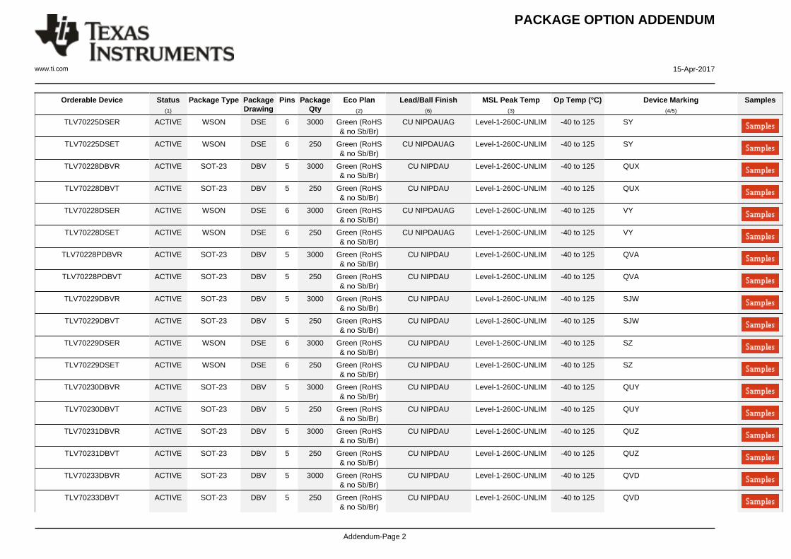
Orderable Device Status(1)
Package Type PackageDrawing
Pins PackageQty
Eco Plan(2)
Lead/Ball Finish(6)
MSL Peak Temp(3)
Op Temp (°C) Device Marking(4/5)
Samples
TLV70225DSER ACTIVE WSON DSE 6 3000 Green (RoHS& no Sb/Br)
CU NIPDAUAG Level-1-260C-UNLIM -40 to 125 SY
TLV70225DSET ACTIVE WSON DSE 6 250 Green (RoHS& no Sb/Br)
CU NIPDAUAG Level-1-260C-UNLIM -40 to 125 SY
TLV70228DBVR ACTIVE SOT-23 DBV 5 3000 Green (RoHS& no Sb/Br)
CU NIPDAU Level-1-260C-UNLIM -40 to 125 QUX
TLV70228DBVT ACTIVE SOT-23 DBV 5 250 Green (RoHS& no Sb/Br)
CU NIPDAU Level-1-260C-UNLIM -40 to 125 QUX
TLV70228DSER ACTIVE WSON DSE 6 3000 Green (RoHS& no Sb/Br)
CU NIPDAUAG Level-1-260C-UNLIM -40 to 125 VY
TLV70228DSET ACTIVE WSON DSE 6 250 Green (RoHS& no Sb/Br)
CU NIPDAUAG Level-1-260C-UNLIM -40 to 125 VY
TLV70228PDBVR ACTIVE SOT-23 DBV 5 3000 Green (RoHS& no Sb/Br)
CU NIPDAU Level-1-260C-UNLIM -40 to 125 QVA
TLV70228PDBVT ACTIVE SOT-23 DBV 5 250 Green (RoHS& no Sb/Br)
CU NIPDAU Level-1-260C-UNLIM -40 to 125 QVA
TLV70229DBVR ACTIVE SOT-23 DBV 5 3000 Green (RoHS& no Sb/Br)
CU NIPDAU Level-1-260C-UNLIM -40 to 125 SJW
TLV70229DBVT ACTIVE SOT-23 DBV 5 250 Green (RoHS& no Sb/Br)
CU NIPDAU Level-1-260C-UNLIM -40 to 125 SJW
TLV70229DSER ACTIVE WSON DSE 6 3000 Green (RoHS& no Sb/Br)
CU NIPDAU Level-1-260C-UNLIM -40 to 125 SZ
TLV70229DSET ACTIVE WSON DSE 6 250 Green (RoHS& no Sb/Br)
CU NIPDAU Level-1-260C-UNLIM -40 to 125 SZ
TLV70230DBVR ACTIVE SOT-23 DBV 5 3000 Green (RoHS& no Sb/Br)
CU NIPDAU Level-1-260C-UNLIM -40 to 125 QUY
TLV70230DBVT ACTIVE SOT-23 DBV 5 250 Green (RoHS& no Sb/Br)
CU NIPDAU Level-1-260C-UNLIM -40 to 125 QUY
TLV70231DBVR ACTIVE SOT-23 DBV 5 3000 Green (RoHS& no Sb/Br)
CU NIPDAU Level-1-260C-UNLIM -40 to 125 QUZ
TLV70231DBVT ACTIVE SOT-23 DBV 5 250 Green (RoHS& no Sb/Br)
CU NIPDAU Level-1-260C-UNLIM -40 to 125 QUZ
TLV70233DBVR ACTIVE SOT-23 DBV 5 3000 Green (RoHS& no Sb/Br)
CU NIPDAU Level-1-260C-UNLIM -40 to 125 QVD
TLV70233DBVT ACTIVE SOT-23 DBV 5 250 Green (RoHS& no Sb/Br)
CU NIPDAU Level-1-260C-UNLIM -40 to 125 QVD

PACKAGE OPTION ADDENDUM
www.ti.com 15-Apr-2017
Addendum-Page 3
Orderable Device Status(1)
Package Type PackageDrawing
Pins PackageQty
Eco Plan(2)
Lead/Ball Finish(6)
MSL Peak Temp(3)
Op Temp (°C) Device Marking(4/5)
Samples
TLV70233DSER ACTIVE WSON DSE 6 3000 Green (RoHS& no Sb/Br)
CU NIPDAUAG Level-1-260C-UNLIM -40 to 125 WK
TLV70233DSET ACTIVE WSON DSE 6 250 Green (RoHS& no Sb/Br)
CU NIPDAUAG Level-1-260C-UNLIM -40 to 125 WK
TLV70233PDBVR ACTIVE SOT-23 DBV 5 3000 Green (RoHS& no Sb/Br)
CU NIPDAU Level-1-260C-UNLIM -40 to 125 SLH
TLV70233PDBVT ACTIVE SOT-23 DBV 5 250 Green (RoHS& no Sb/Br)
CU NIPDAU Level-1-260C-UNLIM -40 to 125 SLH
TLV70235DBVR ACTIVE SOT-23 DBV 5 3000 Green (RoHS& no Sb/Br)
CU NIPDAU Level-1-260C-UNLIM -40 to 125 SDT
TLV70235DBVT ACTIVE SOT-23 DBV 5 250 Green (RoHS& no Sb/Br)
CU NIPDAU Level-1-260C-UNLIM -40 to 125 SDT
TLV70236DSER ACTIVE WSON DSE 6 3000 Green (RoHS& no Sb/Br)
CU NIPDAUAG Level-1-260C-UNLIM -40 to 125 VZ
TLV70236DSET ACTIVE WSON DSE 6 250 Green (RoHS& no Sb/Br)
CU NIPDAUAG Level-1-260C-UNLIM -40 to 125 VZ
TLV70237DBVR ACTIVE SOT-23 DBV 5 3000 Green (RoHS& no Sb/Br)
CU NIPDAU Level-1-260C-UNLIM -40 to 125 QXR
TLV70237DBVT ACTIVE SOT-23 DBV 5 250 Green (RoHS& no Sb/Br)
CU NIPDAU Level-1-260C-UNLIM -40 to 125 QXR
TLV70237DSER ACTIVE WSON DSE 6 3000 Green (RoHS& no Sb/Br)
CU NIPDAU Level-1-260C-UNLIM -40 to 125 D8
TLV70237DSET ACTIVE WSON DSE 6 250 Green (RoHS& no Sb/Br)
CU NIPDAU Level-1-260C-UNLIM -40 to 125 D8
TLV70242PDSER ACTIVE WSON DSE 6 3000 Green (RoHS& no Sb/Br)
CU NIPDAU Level-1-260C-UNLIM -40 to 125 B9
TLV70242PDSET ACTIVE WSON DSE 6 250 Green (RoHS& no Sb/Br)
CU NIPDAU Level-1-260C-UNLIM -40 to 125 B9
TLV70243DSER ACTIVE WSON DSE 6 3000 Green (RoHS& no Sb/Br)
CU NIPDAU Level-1-260C-UNLIM -40 to 125 5Q
TLV70243DSET ACTIVE WSON DSE 6 250 Green (RoHS& no Sb/Br)
CU NIPDAU Level-1-260C-UNLIM -40 to 125 5Q
TLV70245DBVR ACTIVE SOT-23 DBV 5 3000 Green (RoHS& no Sb/Br)
CU NIPDAU Level-1-260C-UNLIM -40 to 125 SCK
TLV70245DBVT ACTIVE SOT-23 DBV 5 250 Green (RoHS& no Sb/Br)
CU NIPDAU Level-1-260C-UNLIM -40 to 125 SCK
PACKAGE OPTION ADDENDUM
www.ti.com 15-Apr-2017
Addendum-Page 4
Orderable Device Status(1)
Package Type PackageDrawing
Pins PackageQty
Eco Plan(2)
Lead/Ball Finish(6)
MSL Peak Temp(3)
Op Temp (°C) Device Marking(4/5)
Samples
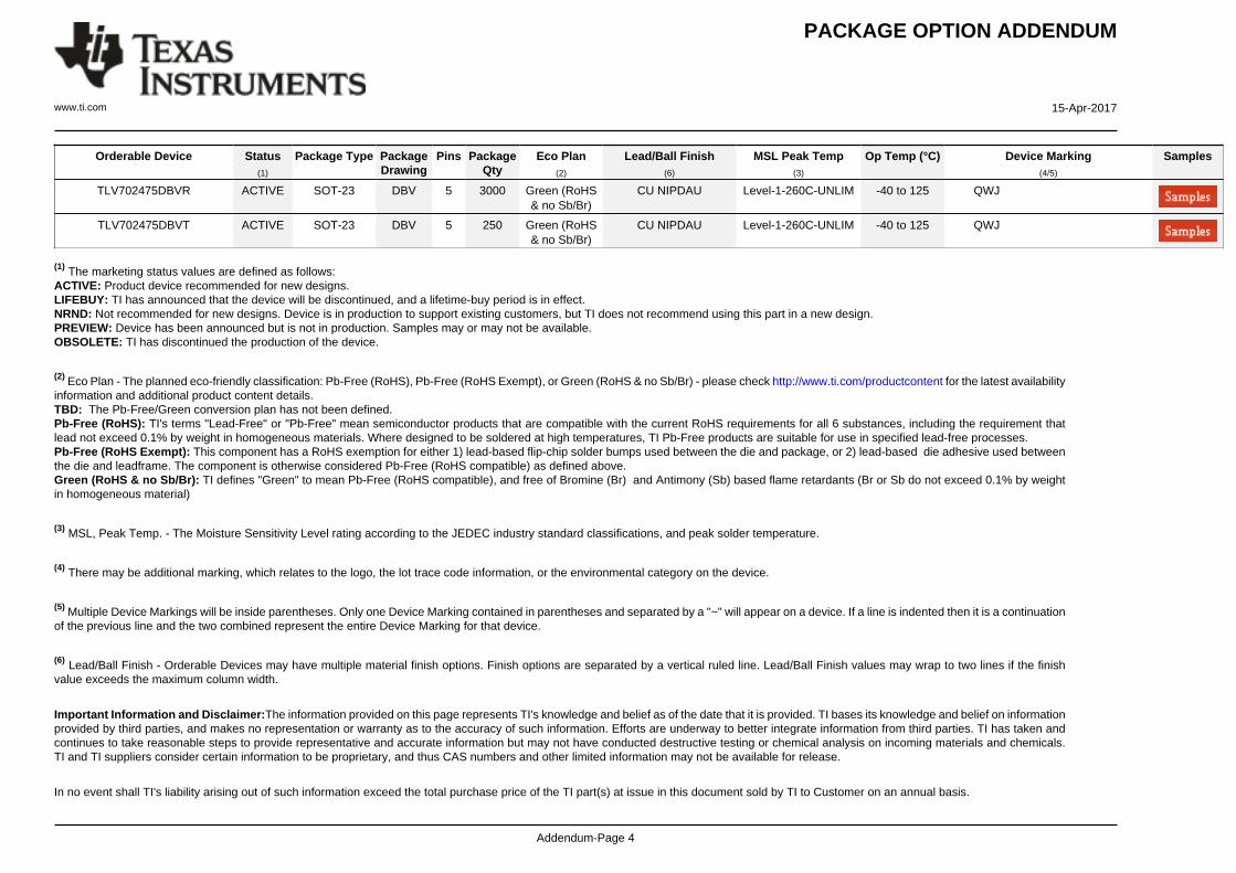
TLV702475DBVR ACTIVE SOT-23 DBV 5 3000 Green (RoHS& no Sb/Br)
CU NIPDAU Level-1-260C-UNLIM -40 to 125 QWJ
TLV702475DBVT ACTIVE SOT-23 DBV 5 250 Green (RoHS& no Sb/Br)
CU NIPDAU Level-1-260C-UNLIM -40 to 125 QWJ
(1) The marketing status values are defined as follows:ACTIVE: Product device recommended for new designs.LIFEBUY: TI has announced that the device will be discontinued, and a lifetime-buy period is in effect.NRND: Not recommended for new designs. Device is in production to support existing customers, but TI does not recommend using this part in a new design.PREVIEW: Device has been announced but is not in production. Samples may or may not be available.OBSOLETE: TI has discontinued the production of the device.
(2) Eco Plan - The planned eco-friendly classification: Pb-Free (RoHS), Pb-Free (RoHS Exempt), or Green (RoHS & no Sb/Br) - please check http://www.ti.com/productcontent for the latest availabilityinformation and additional product content details.TBD: The Pb-Free/Green conversion plan has not been defined.Pb-Free (RoHS): TI's terms "Lead-Free" or "Pb-Free" mean semiconductor products that are compatible with the current RoHS requirements for all 6 substances, including the requirement thatlead not exceed 0.1% by weight in homogeneous materials. Where designed to be soldered at high temperatures, TI Pb-Free products are suitable for use in specified lead-free processes.Pb-Free (RoHS Exempt): This component has a RoHS exemption for either 1) lead-based flip-chip solder bumps used between the die and package, or 2) lead-based die adhesive used betweenthe die and leadframe. The component is otherwise considered Pb-Free (RoHS compatible) as defined above.Green (RoHS & no Sb/Br): TI defines "Green" to mean Pb-Free (RoHS compatible), and free of Bromine (Br) and Antimony (Sb) based flame retardants (Br or Sb do not exceed 0.1% by weightin homogeneous material)
(3) MSL, Peak Temp. - The Moisture Sensitivity Level rating according to the JEDEC industry standard classifications, and peak solder temperature.
(4) There may be additional marking, which relates to the logo, the lot trace code information, or the environmental category on the device.
(5) Multiple Device Markings will be inside parentheses. Only one Device Marking contained in parentheses and separated by a "~" will appear on a device. If a line is indented then it is a continuationof the previous line and the two combined represent the entire Device Marking for that device.
(6) Lead/Ball Finish - Orderable Devices may have multiple material finish options. Finish options are separated by a vertical ruled line. Lead/Ball Finish values may wrap to two lines if the finishvalue exceeds the maximum column width.
Important Information and Disclaimer:The information provided on this page represents TI's knowledge and belief as of the date that it is provided. TI bases its knowledge and belief on informationprovided by third parties, and makes no representation or warranty as to the accuracy of such information. Efforts are underway to better integrate information from third parties. TI has taken andcontinues to take reasonable steps to provide representative and accurate information but may not have conducted destructive testing or chemical analysis on incoming materials and chemicals.TI and TI suppliers consider certain information to be proprietary, and thus CAS numbers and other limited information may not be available for release.
In no event shall TI's liability arising out of such information exceed the total purchase price of the TI part(s) at issue in this document sold by TI to Customer on an annual basis.

PACKAGE OPTION ADDENDUM
www.ti.com 15-Apr-2017
Addendum-Page 5
OTHER QUALIFIED VERSIONS OF TLV702 :
• Automotive: TLV702-Q1
NOTE: Qualified Version Definitions:
• Automotive - Q100 devices qualified for high-reliability automotive applications targeting zero defects

TAPE AND REEL INFORMATION
*All dimensions are nominal
Device PackageType
PackageDrawing
Pins SPQ ReelDiameter
(mm)
ReelWidth
W1 (mm)
A0(mm)
B0(mm)
K0(mm)
P1(mm)
W(mm)
Pin1Quadrant
TLV70212DBVR SOT-23 DBV 5 3000 180.0 8.4 3.2 3.2 1.4 4.0 8.0 Q3
TLV70212DBVR SOT-23 DBV 5 3000 178.0 9.0 3.23 3.17 1.37 4.0 8.0 Q3
TLV70212DBVT SOT-23 DBV 5 250 178.0 8.4 3.23 3.17 1.37 4.0 8.0 Q3
TLV70212DBVT SOT-23 DBV 5 250 180.0 8.4 3.2 3.2 1.4 4.0 8.0 Q3
TLV70213DBVR SOT-23 DBV 5 3000 178.0 9.0 3.23 3.17 1.37 4.0 8.0 Q3
TLV70213DBVT SOT-23 DBV 5 250 178.0 9.0 3.23 3.17 1.37 4.0 8.0 Q3
TLV70215DBVR SOT-23 DBV 5 3000 180.0 8.4 3.2 3.2 1.4 4.0 8.0 Q3
TLV70215DBVR SOT-23 DBV 5 3000 178.0 9.0 3.23 3.17 1.37 4.0 8.0 Q3
TLV70215DBVT SOT-23 DBV 5 250 178.0 8.4 3.23 3.17 1.37 4.0 8.0 Q3
TLV70215DBVT SOT-23 DBV 5 250 180.0 8.4 3.2 3.2 1.4 4.0 8.0 Q3
TLV70215PDBVR SOT-23 DBV 5 3000 178.0 9.0 3.23 3.17 1.37 4.0 8.0 Q3
TLV70215PDBVT SOT-23 DBV 5 250 178.0 8.4 3.23 3.17 1.37 4.0 8.0 Q3
TLV70218DBVR SOT-23 DBV 5 3000 180.0 8.4 3.2 3.2 1.4 4.0 8.0 Q3
TLV70218DBVR SOT-23 DBV 5 3000 180.0 8.4 3.23 3.17 1.37 4.0 8.0 Q3
TLV70218DBVT SOT-23 DBV 5 250 180.0 8.4 3.2 3.2 1.4 4.0 8.0 Q3
TLV70218DBVT SOT-23 DBV 5 250 178.0 8.4 3.3 3.2 1.4 4.0 8.0 Q3
TLV70218DBVT SOT-23 DBV 5 250 180.0 8.4 3.23 3.17 1.37 4.0 8.0 Q3
TLV70220PDBVR SOT-23 DBV 5 3000 178.0 9.0 3.23 3.17 1.37 4.0 8.0 Q3
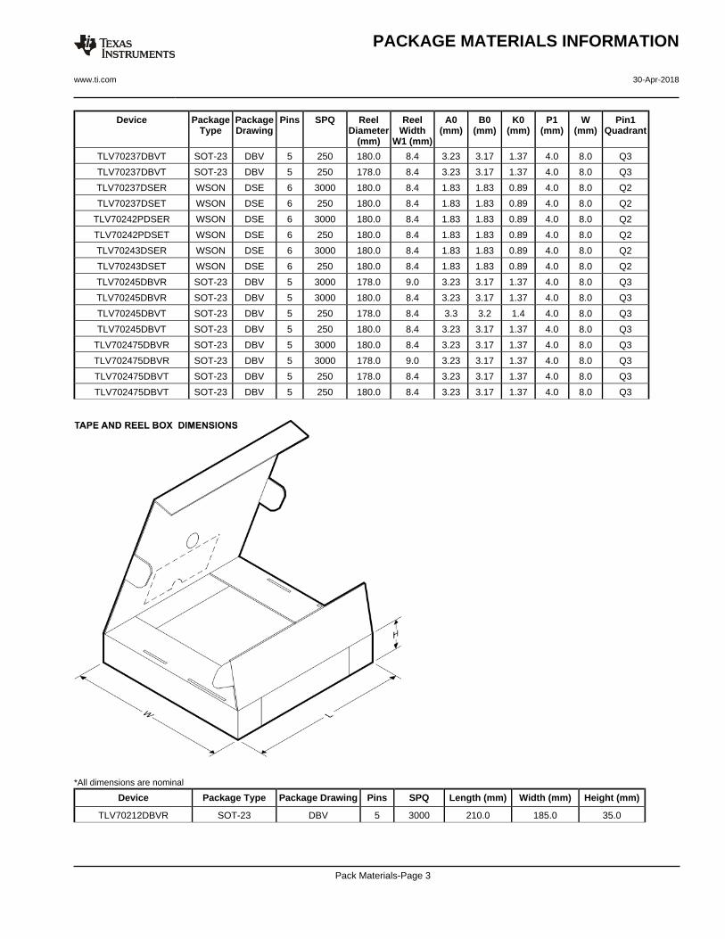
PACKAGE MATERIALS INFORMATION
www.ti.com 30-Apr-2018
Pack Materials-Page 1

Device PackageType
PackageDrawing
Pins SPQ ReelDiameter
(mm)
ReelWidth
W1 (mm)
A0(mm)
B0(mm)
K0(mm)
P1(mm)
W(mm)
Pin1Quadrant
TLV70220PDBVT SOT-23 DBV 5 250 178.0 8.4 3.23 3.17 1.37 4.0 8.0 Q3
TLV70225DBVR SOT-23 DBV 5 3000 178.0 9.0 3.23 3.17 1.37 4.0 8.0 Q3
TLV70225DBVR SOT-23 DBV 5 3000 180.0 8.4 3.23 3.17 1.37 4.0 8.0 Q3
TLV70225DBVT SOT-23 DBV 5 250 178.0 8.4 3.23 3.17 1.37 4.0 8.0 Q3
TLV70225DBVT SOT-23 DBV 5 250 180.0 8.4 3.23 3.17 1.37 4.0 8.0 Q3
TLV70225DSER WSON DSE 6 3000 179.0 8.4 1.8 1.8 1.0 4.0 8.0 Q2
TLV70225DSET WSON DSE 6 250 179.0 8.4 1.8 1.8 1.0 4.0 8.0 Q2
TLV70228DBVR SOT-23 DBV 5 3000 178.0 9.0 3.23 3.17 1.37 4.0 8.0 Q3
TLV70228DBVR SOT-23 DBV 5 3000 180.0 8.4 3.2 3.2 1.4 4.0 8.0 Q3
TLV70228DBVT SOT-23 DBV 5 250 180.0 8.4 3.2 3.2 1.4 4.0 8.0 Q3
TLV70228DBVT SOT-23 DBV 5 250 178.0 8.4 3.23 3.17 1.37 4.0 8.0 Q3
TLV70228DSER WSON DSE 6 3000 179.0 8.4 1.8 1.8 1.0 4.0 8.0 Q2
TLV70228DSET WSON DSE 6 250 179.0 8.4 1.8 1.8 1.0 4.0 8.0 Q2
TLV70228PDBVR SOT-23 DBV 5 3000 180.0 8.4 3.23 3.17 1.37 4.0 8.0 Q3
TLV70228PDBVT SOT-23 DBV 5 250 180.0 8.4 3.23 3.17 1.37 4.0 8.0 Q3
TLV70229DBVR SOT-23 DBV 5 3000 178.0 9.0 3.23 3.17 1.37 4.0 8.0 Q3
TLV70229DBVT SOT-23 DBV 5 250 178.0 8.4 3.23 3.17 1.37 4.0 8.0 Q3
TLV70229DSER WSON DSE 6 3000 180.0 8.4 1.83 1.83 0.89 4.0 8.0 Q2
TLV70229DSET WSON DSE 6 250 180.0 8.4 1.83 1.83 0.89 4.0 8.0 Q2
TLV70230DBVR SOT-23 DBV 5 3000 180.0 8.4 3.23 3.17 1.37 4.0 8.0 Q3
TLV70230DBVR SOT-23 DBV 5 3000 178.0 9.0 3.23 3.17 1.37 4.0 8.0 Q3
TLV70230DBVT SOT-23 DBV 5 250 178.0 8.4 3.23 3.17 1.37 4.0 8.0 Q3
TLV70230DBVT SOT-23 DBV 5 250 180.0 8.4 3.23 3.17 1.37 4.0 8.0 Q3
TLV70231DBVR SOT-23 DBV 5 3000 180.0 8.4 3.23 3.17 1.37 4.0 8.0 Q3
TLV70231DBVR SOT-23 DBV 5 3000 178.0 9.0 3.23 3.17 1.37 4.0 8.0 Q3
TLV70231DBVT SOT-23 DBV 5 250 180.0 8.4 3.23 3.17 1.37 4.0 8.0 Q3
TLV70231DBVT SOT-23 DBV 5 250 178.0 8.4 3.23 3.17 1.37 4.0 8.0 Q3
TLV70233DBVR SOT-23 DBV 5 3000 180.0 8.4 3.2 3.2 1.4 4.0 8.0 Q3
TLV70233DBVT SOT-23 DBV 5 250 178.0 8.4 3.23 3.17 1.37 4.0 8.0 Q3
TLV70233DBVT SOT-23 DBV 5 250 180.0 8.4 3.2 3.2 1.4 4.0 8.0 Q3
TLV70233DBVT SOT-23 DBV 5 250 180.0 8.4 3.23 3.17 1.37 4.0 8.0 Q3
TLV70233DSER WSON DSE 6 3000 179.0 8.4 1.8 1.8 1.0 4.0 8.0 Q2
TLV70233DSET WSON DSE 6 250 179.0 8.4 1.8 1.8 1.0 4.0 8.0 Q2
TLV70233PDBVR SOT-23 DBV 5 3000 178.0 9.0 3.23 3.17 1.37 4.0 8.0 Q3
TLV70233PDBVT SOT-23 DBV 5 250 178.0 8.4 3.23 3.17 1.37 4.0 8.0 Q3
TLV70235DBVR SOT-23 DBV 5 3000 178.0 9.0 3.23 3.17 1.37 4.0 8.0 Q3
TLV70235DBVR SOT-23 DBV 5 3000 180.0 8.4 3.23 3.17 1.37 4.0 8.0 Q3
TLV70235DBVT SOT-23 DBV 5 250 180.0 8.4 3.23 3.17 1.37 4.0 8.0 Q3
TLV70235DBVT SOT-23 DBV 5 250 178.0 8.4 3.23 3.17 1.37 4.0 8.0 Q3
TLV70236DSER WSON DSE 6 3000 179.0 8.4 1.8 1.8 1.0 4.0 8.0 Q2
TLV70236DSET WSON DSE 6 250 179.0 8.4 1.8 1.8 1.0 4.0 8.0 Q2
TLV70237DBVR SOT-23 DBV 5 3000 180.0 8.4 3.23 3.17 1.37 4.0 8.0 Q3
TLV70237DBVR SOT-23 DBV 5 3000 178.0 9.0 3.23 3.17 1.37 4.0 8.0 Q3
PACKAGE MATERIALS INFORMATION
www.ti.com 30-Apr-2018
Pack Materials-Page 2
Device PackageType
PackageDrawing
Pins SPQ ReelDiameter
(mm)
ReelWidth
W1 (mm)
A0(mm)
B0(mm)
K0(mm)
P1(mm)
W(mm)
Pin1Quadrant
TLV70237DBVT SOT-23 DBV 5 250 180.0 8.4 3.23 3.17 1.37 4.0 8.0 Q3
TLV70237DBVT SOT-23 DBV 5 250 178.0 8.4 3.23 3.17 1.37 4.0 8.0 Q3
TLV70237DSER WSON DSE 6 3000 180.0 8.4 1.83 1.83 0.89 4.0 8.0 Q2
TLV70237DSET WSON DSE 6 250 180.0 8.4 1.83 1.83 0.89 4.0 8.0 Q2
TLV70242PDSER WSON DSE 6 3000 180.0 8.4 1.83 1.83 0.89 4.0 8.0 Q2
TLV70242PDSET WSON DSE 6 250 180.0 8.4 1.83 1.83 0.89 4.0 8.0 Q2
TLV70243DSER WSON DSE 6 3000 180.0 8.4 1.83 1.83 0.89 4.0 8.0 Q2
TLV70243DSET WSON DSE 6 250 180.0 8.4 1.83 1.83 0.89 4.0 8.0 Q2
TLV70245DBVR SOT-23 DBV 5 3000 178.0 9.0 3.23 3.17 1.37 4.0 8.0 Q3
TLV70245DBVR SOT-23 DBV 5 3000 180.0 8.4 3.23 3.17 1.37 4.0 8.0 Q3
TLV70245DBVT SOT-23 DBV 5 250 178.0 8.4 3.3 3.2 1.4 4.0 8.0 Q3
TLV70245DBVT SOT-23 DBV 5 250 180.0 8.4 3.23 3.17 1.37 4.0 8.0 Q3
TLV702475DBVR SOT-23 DBV 5 3000 180.0 8.4 3.23 3.17 1.37 4.0 8.0 Q3
TLV702475DBVR SOT-23 DBV 5 3000 178.0 9.0 3.23 3.17 1.37 4.0 8.0 Q3
TLV702475DBVT SOT-23 DBV 5 250 178.0 8.4 3.23 3.17 1.37 4.0 8.0 Q3
TLV702475DBVT SOT-23 DBV 5 250 180.0 8.4 3.23 3.17 1.37 4.0 8.0 Q3
*All dimensions are nominal
Device Package Type Package Drawing Pins SPQ Length (mm) Width (mm) Height (mm)
TLV70212DBVR SOT-23 DBV 5 3000 210.0 185.0 35.0
PACKAGE MATERIALS INFORMATION
www.ti.com 30-Apr-2018
Pack Materials-Page 3

Device Package Type Package Drawing Pins SPQ Length (mm) Width (mm) Height (mm)
TLV70212DBVR SOT-23 DBV 5 3000 180.0 180.0 18.0
TLV70212DBVT SOT-23 DBV 5 250 180.0 180.0 18.0
TLV70212DBVT SOT-23 DBV 5 250 210.0 185.0 35.0
TLV70213DBVR SOT-23 DBV 5 3000 180.0 180.0 18.0
TLV70213DBVT SOT-23 DBV 5 250 180.0 180.0 18.0
TLV70215DBVR SOT-23 DBV 5 3000 210.0 185.0 35.0
TLV70215DBVR SOT-23 DBV 5 3000 180.0 180.0 18.0
TLV70215DBVT SOT-23 DBV 5 250 180.0 180.0 18.0
TLV70215DBVT SOT-23 DBV 5 250 210.0 185.0 35.0
TLV70215PDBVR SOT-23 DBV 5 3000 180.0 180.0 18.0
TLV70215PDBVT SOT-23 DBV 5 250 180.0 180.0 18.0
TLV70218DBVR SOT-23 DBV 5 3000 210.0 185.0 35.0
TLV70218DBVR SOT-23 DBV 5 3000 183.0 183.0 20.0
TLV70218DBVT SOT-23 DBV 5 250 210.0 185.0 35.0
TLV70218DBVT SOT-23 DBV 5 250 180.0 180.0 18.0
TLV70218DBVT SOT-23 DBV 5 250 183.0 183.0 20.0
TLV70220PDBVR SOT-23 DBV 5 3000 180.0 180.0 18.0
TLV70220PDBVT SOT-23 DBV 5 250 180.0 180.0 18.0
TLV70225DBVR SOT-23 DBV 5 3000 180.0 180.0 18.0
TLV70225DBVR SOT-23 DBV 5 3000 183.0 183.0 20.0
TLV70225DBVT SOT-23 DBV 5 250 180.0 180.0 18.0
TLV70225DBVT SOT-23 DBV 5 250 183.0 183.0 20.0
TLV70225DSER WSON DSE 6 3000 203.0 203.0 35.0
TLV70225DSET WSON DSE 6 250 203.0 203.0 35.0
TLV70228DBVR SOT-23 DBV 5 3000 180.0 180.0 18.0
TLV70228DBVR SOT-23 DBV 5 3000 210.0 185.0 35.0
TLV70228DBVT SOT-23 DBV 5 250 210.0 185.0 35.0
TLV70228DBVT SOT-23 DBV 5 250 180.0 180.0 18.0
TLV70228DSER WSON DSE 6 3000 203.0 203.0 35.0
TLV70228DSET WSON DSE 6 250 203.0 203.0 35.0
TLV70228PDBVR SOT-23 DBV 5 3000 183.0 183.0 20.0
TLV70228PDBVT SOT-23 DBV 5 250 183.0 183.0 20.0
TLV70229DBVR SOT-23 DBV 5 3000 180.0 180.0 18.0
TLV70229DBVT SOT-23 DBV 5 250 180.0 180.0 18.0
TLV70229DSER WSON DSE 6 3000 183.0 183.0 20.0
TLV70229DSET WSON DSE 6 250 183.0 183.0 20.0
TLV70230DBVR SOT-23 DBV 5 3000 183.0 183.0 20.0
TLV70230DBVR SOT-23 DBV 5 3000 180.0 180.0 18.0
TLV70230DBVT SOT-23 DBV 5 250 180.0 180.0 18.0
TLV70230DBVT SOT-23 DBV 5 250 183.0 183.0 20.0
TLV70231DBVR SOT-23 DBV 5 3000 183.0 183.0 20.0
TLV70231DBVR SOT-23 DBV 5 3000 180.0 180.0 18.0
TLV70231DBVT SOT-23 DBV 5 250 183.0 183.0 20.0
TLV70231DBVT SOT-23 DBV 5 250 180.0 180.0 18.0
PACKAGE MATERIALS INFORMATION
www.ti.com 30-Apr-2018
Pack Materials-Page 4
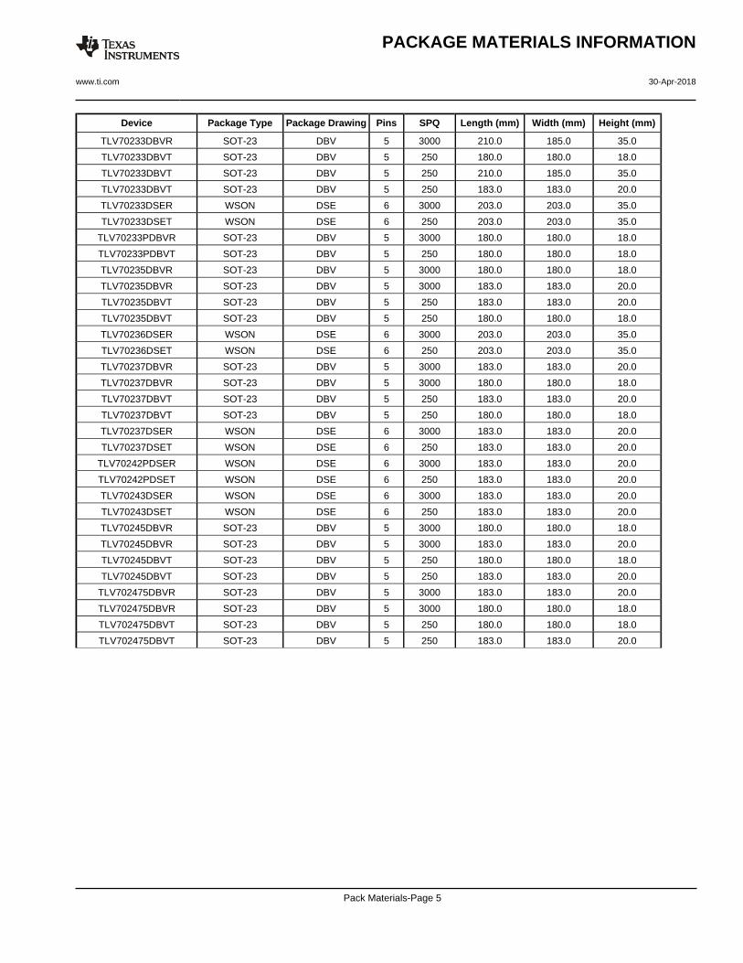
Device Package Type Package Drawing Pins SPQ Length (mm) Width (mm) Height (mm)
TLV70233DBVR SOT-23 DBV 5 3000 210.0 185.0 35.0
TLV70233DBVT SOT-23 DBV 5 250 180.0 180.0 18.0
TLV70233DBVT SOT-23 DBV 5 250 210.0 185.0 35.0
TLV70233DBVT SOT-23 DBV 5 250 183.0 183.0 20.0
TLV70233DSER WSON DSE 6 3000 203.0 203.0 35.0
TLV70233DSET WSON DSE 6 250 203.0 203.0 35.0
TLV70233PDBVR SOT-23 DBV 5 3000 180.0 180.0 18.0
TLV70233PDBVT SOT-23 DBV 5 250 180.0 180.0 18.0
TLV70235DBVR SOT-23 DBV 5 3000 180.0 180.0 18.0
TLV70235DBVR SOT-23 DBV 5 3000 183.0 183.0 20.0
TLV70235DBVT SOT-23 DBV 5 250 183.0 183.0 20.0
TLV70235DBVT SOT-23 DBV 5 250 180.0 180.0 18.0
TLV70236DSER WSON DSE 6 3000 203.0 203.0 35.0
TLV70236DSET WSON DSE 6 250 203.0 203.0 35.0
TLV70237DBVR SOT-23 DBV 5 3000 183.0 183.0 20.0
TLV70237DBVR SOT-23 DBV 5 3000 180.0 180.0 18.0
TLV70237DBVT SOT-23 DBV 5 250 183.0 183.0 20.0
TLV70237DBVT SOT-23 DBV 5 250 180.0 180.0 18.0
TLV70237DSER WSON DSE 6 3000 183.0 183.0 20.0
TLV70237DSET WSON DSE 6 250 183.0 183.0 20.0
TLV70242PDSER WSON DSE 6 3000 183.0 183.0 20.0
TLV70242PDSET WSON DSE 6 250 183.0 183.0 20.0
TLV70243DSER WSON DSE 6 3000 183.0 183.0 20.0
TLV70243DSET WSON DSE 6 250 183.0 183.0 20.0
TLV70245DBVR SOT-23 DBV 5 3000 180.0 180.0 18.0
TLV70245DBVR SOT-23 DBV 5 3000 183.0 183.0 20.0
TLV70245DBVT SOT-23 DBV 5 250 180.0 180.0 18.0
TLV70245DBVT SOT-23 DBV 5 250 183.0 183.0 20.0
TLV702475DBVR SOT-23 DBV 5 3000 183.0 183.0 20.0
TLV702475DBVR SOT-23 DBV 5 3000 180.0 180.0 18.0
TLV702475DBVT SOT-23 DBV 5 250 180.0 180.0 18.0
TLV702475DBVT SOT-23 DBV 5 250 183.0 183.0 20.0
PACKAGE MATERIALS INFORMATION
www.ti.com 30-Apr-2018
Pack Materials-Page 5


www.ti.com
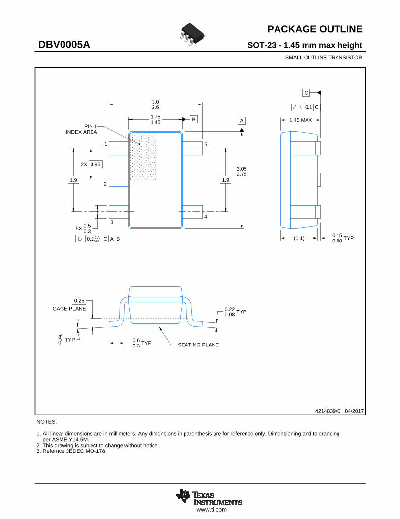
PACKAGE OUTLINE
C
TYP0.220.08
0.25
3.02.6
2X 0.95
1.9
1.45 MAX
TYP0.150.00
5X 0.50.3
TYP0.60.3
TYP80
1.9
A
3.052.75
B1.751.45
(1.1)
SOT-23 - 1.45 mm max heightDBV0005ASMALL OUTLINE TRANSISTOR
4214839/C 04/2017
NOTES: 1. All linear dimensions are in millimeters. Any dimensions in parenthesis are for reference only. Dimensioning and tolerancing per ASME Y14.5M.2. This drawing is subject to change without notice.3. Refernce JEDEC MO-178.
0.2 C A B
1
34
5
2
INDEX AREAPIN 1
GAGE PLANE
SEATING PLANE
0.1 C
SCALE 4.000
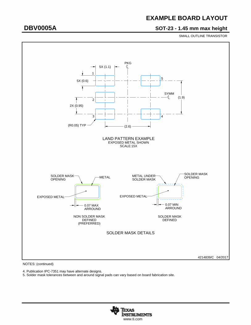
www.ti.com
EXAMPLE BOARD LAYOUT
0.07 MAXARROUND
0.07 MINARROUND
5X (1.1)
5X (0.6)
(2.6)
(1.9)
2X (0.95)
(R0.05) TYP
4214839/C 04/2017
SOT-23 - 1.45 mm max heightDBV0005ASMALL OUTLINE TRANSISTOR
NOTES: (continued) 4. Publication IPC-7351 may have alternate designs. 5. Solder mask tolerances between and around signal pads can vary based on board fabrication site.
SYMM
LAND PATTERN EXAMPLEEXPOSED METAL SHOWN
SCALE:15X
PKG
1
3 4
5
2
SOLDER MASKOPENINGMETAL UNDER
SOLDER MASK
SOLDER MASKDEFINED
EXPOSED METAL
METALSOLDER MASKOPENING
NON SOLDER MASKDEFINED
(PREFERRED)
SOLDER MASK DETAILS
EXPOSED METAL
www.ti.com
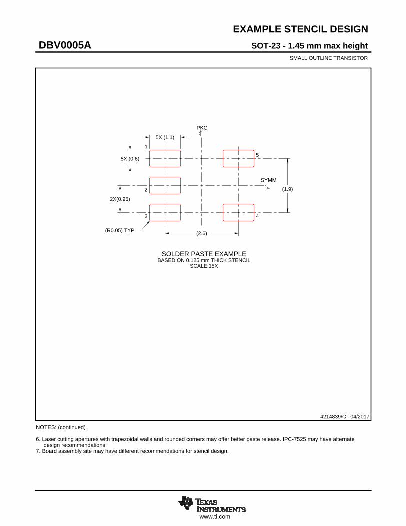
EXAMPLE STENCIL DESIGN
(2.6)
(1.9)
2X(0.95)
5X (1.1)
5X (0.6)
(R0.05) TYP
SOT-23 - 1.45 mm max heightDBV0005ASMALL OUTLINE TRANSISTOR
4214839/C 04/2017
NOTES: (continued) 6. Laser cutting apertures with trapezoidal walls and rounded corners may offer better paste release. IPC-7525 may have alternate design recommendations. 7. Board assembly site may have different recommendations for stencil design.
SOLDER PASTE EXAMPLEBASED ON 0.125 mm THICK STENCIL
SCALE:15X
SYMM
PKG
1
3 4
5
2
IMPORTANT NOTICE
Texas Instruments Incorporated (TI) reserves the right to make corrections, enhancements, improvements and other changes to itssemiconductor products and services per JESD46, latest issue, and to discontinue any product or service per JESD48, latest issue. Buyersshould obtain the latest relevant information before placing orders and should verify that such information is current and complete.TI’s published terms of sale for semiconductor products (http://www.ti.com/sc/docs/stdterms.htm) apply to the sale of packaged integratedcircuit products that TI has qualified and released to market. Additional terms may apply to the use or sale of other types of TI products andservices.Reproduction of significant portions of TI information in TI data sheets is permissible only if reproduction is without alteration and isaccompanied by all associated warranties, conditions, limitations, and notices. TI is not responsible or liable for such reproduceddocumentation. Information of third parties may be subject to additional restrictions. Resale of TI products or services with statementsdifferent from or beyond the parameters stated by TI for that product or service voids all express and any implied warranties for theassociated TI product or service and is an unfair and deceptive business practice. TI is not responsible or liable for any such statements.Buyers and others who are developing systems that incorporate TI products (collectively, “Designers”) understand and agree that Designersremain responsible for using their independent analysis, evaluation and judgment in designing their applications and that Designers havefull and exclusive responsibility to assure the safety of Designers' applications and compliance of their applications (and of all TI productsused in or for Designers’ applications) with all applicable regulations, laws and other applicable requirements. Designer represents that, withrespect to their applications, Designer has all the necessary expertise to create and implement safeguards that (1) anticipate dangerousconsequences of failures, (2) monitor failures and their consequences, and (3) lessen the likelihood of failures that might cause harm andtake appropriate actions. Designer agrees that prior to using or distributing any applications that include TI products, Designer willthoroughly test such applications and the functionality of such TI products as used in such applications.TI’s provision of technical, application or other design advice, quality characterization, reliability data or other services or information,including, but not limited to, reference designs and materials relating to evaluation modules, (collectively, “TI Resources”) are intended toassist designers who are developing applications that incorporate TI products; by downloading, accessing or using TI Resources in anyway, Designer (individually or, if Designer is acting on behalf of a company, Designer’s company) agrees to use any particular TI Resourcesolely for this purpose and subject to the terms of this Notice.TI’s provision of TI Resources does not expand or otherwise alter TI’s applicable published warranties or warranty disclaimers for TIproducts, and no additional obligations or liabilities arise from TI providing such TI Resources. TI reserves the right to make corrections,enhancements, improvements and other changes to its TI Resources. TI has not conducted any testing other than that specificallydescribed in the published documentation for a particular TI Resource.Designer is authorized to use, copy and modify any individual TI Resource only in connection with the development of applications thatinclude the TI product(s) identified in such TI Resource. NO OTHER LICENSE, EXPRESS OR IMPLIED, BY ESTOPPEL OR OTHERWISETO ANY OTHER TI INTELLECTUAL PROPERTY RIGHT, AND NO LICENSE TO ANY TECHNOLOGY OR INTELLECTUAL PROPERTYRIGHT OF TI OR ANY THIRD PARTY IS GRANTED HEREIN, including but not limited to any patent right, copyright, mask work right, orother intellectual property right relating to any combination, machine, or process in which TI products or services are used. Informationregarding or referencing third-party products or services does not constitute a license to use such products or services, or a warranty orendorsement thereof. Use of TI Resources may require a license from a third party under the patents or other intellectual property of thethird party, or a license from TI under the patents or other intellectual property of TI.TI RESOURCES ARE PROVIDED “AS IS” AND WITH ALL FAULTS. TI DISCLAIMS ALL OTHER WARRANTIES ORREPRESENTATIONS, EXPRESS OR IMPLIED, REGARDING RESOURCES OR USE THEREOF, INCLUDING BUT NOT LIMITED TOACCURACY OR COMPLETENESS, TITLE, ANY EPIDEMIC FAILURE WARRANTY AND ANY IMPLIED WARRANTIES OFMERCHANTABILITY, FITNESS FOR A PARTICULAR PURPOSE, AND NON-INFRINGEMENT OF ANY THIRD PARTY INTELLECTUALPROPERTY RIGHTS. TI SHALL NOT BE LIABLE FOR AND SHALL NOT DEFEND OR INDEMNIFY DESIGNER AGAINST ANY CLAIM,INCLUDING BUT NOT LIMITED TO ANY INFRINGEMENT CLAIM THAT RELATES TO OR IS BASED ON ANY COMBINATION OFPRODUCTS EVEN IF DESCRIBED IN TI RESOURCES OR OTHERWISE. IN NO EVENT SHALL TI BE LIABLE FOR ANY ACTUAL,DIRECT, SPECIAL, COLLATERAL, INDIRECT, PUNITIVE, INCIDENTAL, CONSEQUENTIAL OR EXEMPLARY DAMAGES INCONNECTION WITH OR ARISING OUT OF TI RESOURCES OR USE THEREOF, AND REGARDLESS OF WHETHER TI HAS BEENADVISED OF THE POSSIBILITY OF SUCH DAMAGES.Unless TI has explicitly designated an individual product as meeting the requirements of a particular industry standard (e.g., ISO/TS 16949and ISO 26262), TI is not responsible for any failure to meet such industry standard requirements.Where TI specifically promotes products as facilitating functional safety or as compliant with industry functional safety standards, suchproducts are intended to help enable customers to design and create their own applications that meet applicable functional safety standardsand requirements. Using products in an application does not by itself establish any safety features in the application. Designers mustensure compliance with safety-related requirements and standards applicable to their applications. Designer may not use any TI products inlife-critical medical equipment unless authorized officers of the parties have executed a special contract specifically governing such use.Life-critical medical equipment is medical equipment where failure of such equipment would cause serious bodily injury or death (e.g., lifesupport, pacemakers, defibrillators, heart pumps, neurostimulators, and implantables). Such equipment includes, without limitation, allmedical devices identified by the U.S. Food and Drug Administration as Class III devices and equivalent classifications outside the U.S.TI may expressly designate certain products as completing a particular qualification (e.g., Q100, Military Grade, or Enhanced Product).Designers agree that it has the necessary expertise to select the product with the appropriate qualification designation for their applicationsand that proper product selection is at Designers’ own risk. Designers are solely responsible for compliance with all legal and regulatoryrequirements in connection with such selection.Designer will fully indemnify TI and its representatives against any damages, costs, losses, and/or liabilities arising out of Designer’s non-compliance with the terms and provisions of this Notice.
Mailing Address: Texas Instruments, Post Office Box 655303, Dallas, Texas 75265Copyright © 2018, Texas Instruments Incorporated
Related Documents