Open access to the Proceedings of the 22nd USENIX Security Symposium is sponsored by USENIX This paper is included in the Proceedings of the 22nd USENIX Security Symposium. August 14–16, 2013 • Washington, D.C., USA ISBN 978-1-931971-03-4 Securing Computer Hardware Using 3D Integrated Circuit (IC) Technology and Split Manufacturing for Obfuscation Frank Imeson, Ariq Emtenan, Siddharth Garg, and Mahesh V. Tripunitara, University of Waterloo

Welcome message from author
This document is posted to help you gain knowledge. Please leave a comment to let me know what you think about it! Share it to your friends and learn new things together.
Transcript

Open access to the Proceedings of the 22nd USENIX Security Symposium
is sponsored by USENIX
This paper is included in the Proceedings of the 22nd USENIX Security Symposium.August 14–16, 2013 • Washington, D.C., USA
ISBN 978-1-931971-03-4
Securing Computer Hardware Using 3D Integrated Circuit (IC) Technology and
Split Manufacturing for ObfuscationFrank Imeson, Ariq Emtenan, Siddharth Garg, and Mahesh V. Tripunitara,
University of Waterloo
USENIX Association 22nd USENIX Security Symposium 495
Securing Computer Hardware Using 3D Integrated Circuit (IC) Technologyand Split Manufacturing for Obfuscation
Frank Imeson, Ariq Emtenan, Siddharth Garg, and Mahesh V. Tripunitara
ECE, University of Waterloo, Canada{fcimeson,aemtenan,siddharth.garg,tripunit}@uwaterloo.ca
Abstract
The fabrication of digital Integrated Circuits (ICs) is in-creasingly outsourced. Given this trend, security is rec-ognized as an important issue. The threat agent is anattacker at the IC foundry that has information about thecircuit and inserts covert, malicious circuitry. The use of3D IC technology has been suggested as a possible tech-nique to counter this threat. However, to our knowledge,there is no prior work on how such technology can beused effectively. We propose a way to use 3D IC tech-nology for security in this context. Specifically, we ob-fuscate the circuit by lifting wires to a trusted tier, whichis fabricated separately. This is referred to as split man-ufacturing. For this setting, we provide a precise notionof security, that we call k-security, and a characterizationof the underlying computational problems and their com-plexity. We further propose a concrete approach for iden-tifying sets of wires to be lifted, and the correspondingsecurity they provide. We conclude with a comprehen-sive empirical assessment with benchmark circuits thathighlights the security versus cost trade-offs introducedby 3D IC based circuit obfuscation.
1 Introduction
The security of digital integrated circuits (ICs), the build-ing blocks of modern computer hardware systems, canbe compromised by covertly inserted malicious circuits.The threat from such maliciously inserted hardware isof increasing concern to government and military agen-cies [2] and commercial semiconductor vendors. Re-cently, Skorobogatov et al. [28] demonstrated the pres-ence of a backdoor in a military grade FPGA manufac-tured by Actel that enabled access to configuration dataon the chip. The authors initially conjectured that thebackdoor was maliciously inserted since the key used totrigger the backdoor was undocumented. Actel has sinceclarified that the backdoor was inserted by design for in-
ternal test purposes [23]. Nonetheless, this incident hasfurther heightened the perceived threat from maliciouslyinserted hardware, and effective counter-measures to de-ter or prevent such attacks are of increasing importance.
The threat of maliciously inserted hardware arisesfrom two factors. First, owing to their complexity, digitalICs are designed at sites across the world. In addition,parts of the design are often outsourced or purchasedfrom external vendors. Second, a majority of semicon-ductor design companies are fabless, i.e., they outsourceIC manufacturing to a potentially untrusted external fab-rication facility (or foundry). Both factors make it easierfor a malicious attacker in a design team or a maliciousfoundry (or a collusion between the two) to insert covertcircuitry in a digital IC.
Three-dimensional (3D) integration, an emerging ICmanufacturing technology, is a promising technique toenhance the security of computer hardware. A 3D ICconsists of two or more independently manufactured ICsthat are vertically stacked on top of each other — eachIC in the stack is referred to as a tier. Interconnectionsbetween the tiers are accomplished using vertical metalpillars referred to as through-silicon vias (TSV).
3D IC manufacturing can potentially enhance hard-ware security since each tier can be manufactured in aseparate IC foundry, and vertically stacked in a securefacility. Thus, a malicious attacker at any one foundryhas an incomplete view of the entire circuit, reducing theattacker’s ability to alter the circuit functionality in a de-sired manner.
Tezarron, a leading commercial provider of 3D stack-ing capabilities, has alluded to the enhanced security of-fered by 3D integration in a white paper [1]. The whitepaper notes that “A multi-layer circuit may be dividedamong the layers in such a way that the function of eachlayer becomes obscure. Assuming that the TSV connec-tions are extremely fine and abundant, elements can bescattered among the layers in apparently random fash-ion.” However, the paper does not provide any formal
496 22nd USENIX Security Symposium USENIX Association
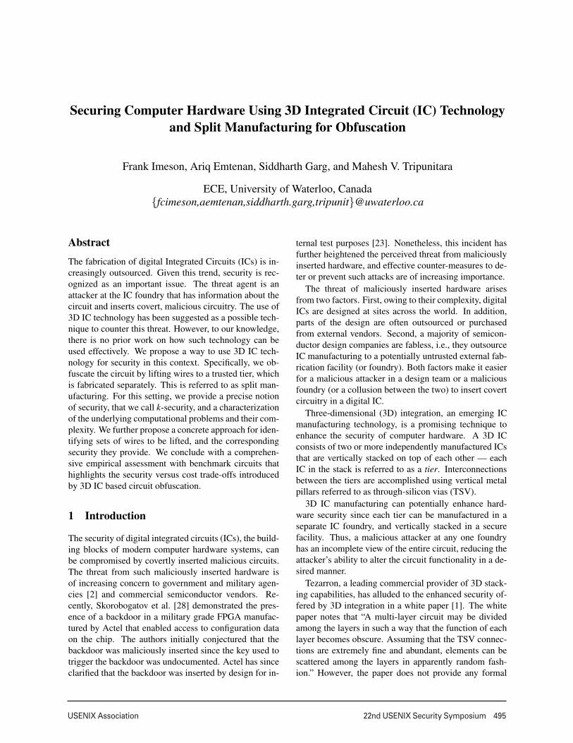
Silicon
Unlifted Wires
Bond Points Lifted Wires
Transistors/Gates
IO Pins
Bottom Tier(Un-Trusted)
Top Tier(Trusted)
Figure 1: A two tier 3D IC. In this instance, the top tier isan interposer, i.e., it only implements metal wires, whilethe bottom tier has both transistors/gates and wires.
notion of security for split manufacturing, nor does itpropose techniques to quantify security or achieve a cer-tain security level. These are the open challenges that weaddress in this paper.
Our threat model assumes a malicious attacker in anIC foundry who wants to modify the functionality of adigital IC in a specific, targeted manner. The attack pro-posed by King et al. [19] modifies the state of hardwareregisters in a processor to raise the privilege level of theattacker — this is an example of a targeted attack since itrequires the attacker to determine the gate or wire in thecircuit that corresponds to the privilege bit. Fault inser-tion attacks in cryptographic hardware also require thatcertain vulnerable bits be targeted. For example, it hasbeen shown that if the LSB bit of the 14th round of aDES implementation is set to logic zero, the secret keycan be recovered in as few as two messages [9]. How-ever, to succeed, the attacker must be able to determinewhich gate corresponds to the LSB bit of the 14th round.
To effect a targeted attack, an attacker must first iden-tify specific logic gates or wires in the circuit that im-plement the functionality that he wants to monitor and/ormodify; for example, the gate or wire that correspondsto the privilege bit for the privilege escalation attack pro-posed in [19]. A malicious foundry can identify the func-tionality of every gate and wire in the circuit if it gets tofabricate the entire chip, i.e., if a conventional planar, 2Dfabrication process is used. On the other hand, as weshow in this paper, 3D integration significantly reducesthe ability of an attacker in a malicious foundry to cor-rectly identify gates or wires in the circuit that he wantsto attack.
The specific 3D integration technology that we exploitin this work, since it is the only one that is currently in
large volume commercial production [8], splits a designinto two tiers. The bottom tier consists of digital logicgates and metal wires used to interconnect logic gates.The top tier, also referred to as an interposer, only con-sists of metal wires that provide additional connectionsbetween logic gates on the bottom tier.
The bottom tier — this tier is expensive to fabricatesince it implements active transistor devices and passivemetal — is sent to an external, untrusted foundry for fab-rication. This is referred to as the untrusted tier. The toptier implements only passive metal and can be fabricatedat lower cost in a trusted fabrication facility. We refer tothis tier as the trusted tier.
Assume, for the sake of argument, that all interconnec-tions between logic gates are implemented on the trustedtier, the attacker (who only has access to the untrustedtier) observes only a “sea” of disconnected digital logicgates. From the perspective of the attacker, gates of thesame type, for example all NAND gates, are therefore in-distinguishable from each other. (Assuming that the rel-ative size or placement of gates reveals no informationabout interconnections between gates. This is addressedin Section 4.) Assume also that the attacker wants to at-tack a specific NAND gate in the circuit, and not just anyNAND gate. The attacker now has two choices: (a) theattacker could randomly pick one NAND gate to attackfrom the set of indistinguishable NAND gates, and onlysucceed in the attack with a certain probability; or (b) theattacker could attack all indistinguishable NAND gates,primarily in cases where the attacker wants to monitorbut not modify gates in the circuit, at the expense of alarger malicious circuit and thus, an increased likelihoodof the attack being detected. In either instance, the at-tacker’s ability to effect a malicious, targeted attack onthe circuit is significantly hindered. We refer to this tech-nique as circuit obfuscation.
In general, we define a k-secure gate as one that, fromthe attacker’s perspective, cannot be distinguished fromk− 1 other gates in the circuit. Furthermore, a k-securecircuit is defined as one in which each gate is at leastk-secure.
Contributions We make the following contributions:
• We propose a concrete way of leveraging 3D ICtechnology to secure digital ICs from an active at-tacker at the foundry. Whereas the use of 3D ICtechnology for security has been alluded to before,we are not aware of prior work like ours that dis-cusses how it can be used meaningfully.
• We propose a formal notion of security in this con-text that we call k-security. We give a precise char-acterization of the underlying technical problems —computing k-security and deciding which wires tolift — and identify their computational complexity.
USENIX Association 22nd USENIX Security Symposium 497
• We have devised a concrete approach to address-ing the problem of lifting wires, which comprises agreedy heuristic to identify a candidate set of wiresto be lifted, and the use of a constraint (SAT) solverto compute k-security.
• We have conducted a thorough empirical assess-ment of our approach on benchmark circuits, in-cluding a case-study of a DES circuit, that illustratesthe inability of an attacker to effectively attack cir-cuits secured using 3D IC based obfuscation.
2 Preliminaries and Related Work
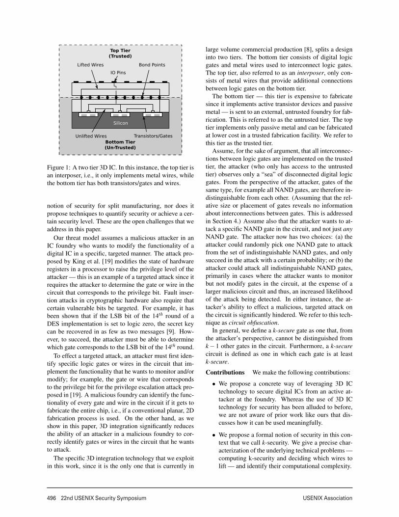
Synthesis
TechnologyLibrary
HDL Codealways @(posedge clk) for(i=0;i<33;i=i+1) key_c_r[i+1] <= #1 key_c_r[i];
Wire Lifting
Netlist
Unlifted Netlist Lifted Wires
Placement and Routing
Layout Layout
Bottom Tier Top Tier
Final Product
Fabrication
StackingMaliciousAttacker
MaliciousObserver
Trusted
Fabrication
Figure 2: Secure 3D IC design and fabrication flow.
In this section, we overview the IC manufacturing pro-cess in the specific context of 3D integration, and discussthe attack model that we assume in this paper. We alsodiscuss related work on hardware security including bothattacks and countermeasures, and on the use 3D integra-tion for enhancing the security of computer hardware.
2.1 3D IC Design and FabricationDigital ICs consist of a network of inter-connected dig-ital logic gates. This network of gates is often referredto as a netlist. Digital logic gates are built using com-plementary metal-oxide-semiconductor (CMOS) transis-
tors. In a conventional planar/2D IC, CMOS transistors,and by extension digital logic gates, lie in a single layerof silicon. In addition, there are several layers of metalwires used to inter-connect the gates.
3D integration enables the vertical stacking of two ormore planar ICs. Each IC in the vertical stack is referredto as a tier. Vertical interconnects (TSVs) are providedto allow the transistors and metal wires in each tier toconnect to each other.
The initial motivation for 3D integration came fromthe potential reduction in the average distance betweenlogic gates — in a 3D IC, the third, vertical dimensioncan be used to achieve a tighter packing of logic gates [6].However, a number of issues, including high power den-sity, temperature and cost, have plagued high volume,commercial availability of logic-on-logic 3D ICs [13].
A more practical 3D IC technology that has beendemonstrated in a commercial product (a XilinxFPGA [8]) is shown in Figure 1. It consists of two tiers.The bottom tier contains both transistors/gates and metalwires, while the top tier, the interposer, contains onlymetal wires. The two tiers are interfaced using uniformlyspaced metallic bond-points. TSVs make use of thesebond-points to provide connections between wires in thetop and bottom tiers. This technology has also been re-ferred to as 2.5D integration [14]. In the rest of this pa-per, we use 3D instead of 2.5D since our techniques caneasily be generalized to full 3D.
Since the bottom tier consists of CMOS transistors, itis fabricated at one of the few foundries worldwide withadvanced lithographic capabilities at high cost. The toptier, i.e., the interposer, only contains passive metal andcan be fabricated at significantly reduced cost [21].
Figure 2 shows a 3D IC design flow with appropri-ate modifications for security. The design flow beginswith the design specified using a hardware descriptionlanguage (HDL), which is then synthesized to a netlist ofgates. The types of gates allowed in the gate netlist arespecified in a technology library.
In the wire lifting stage, the edges (or wires) in thenetlist that are to be implemented on the top tier are se-lected. These are referred to as lifted wires. The rest ofthe netlist, implemented on the bottom tier, is referred toas the unlifted netlist and consists of unlifted gates andunlifted wires.
The unlifted gates are then placed on the surface ofthe bottom tier, i.e., the (x,y) co-ordinates for each gateare selected. Unlifted wires are routed using the bottomtier metal layers. Two bond-points are selected for ev-ery lifted wire; one each for the two gates that the wireconnects. The gates are connected to the correspond-ing bond-points. Finally, lifted wires are routed betweenpairs of bond-points in the top tier using the top tier rout-ing resources.
498 22nd USENIX Security Symposium USENIX Association
Finally, the two tiers are fabricated at separatefoundries. The chips from the two foundries are verti-cally stacked to create the final 3D IC chip that is shippedto the vendor.
We now discuss the attack model that we address inthis paper, in the context of the 3D design and fabricationflow outlined above.
2.2 Attack ModelThe attack model that we address in this paper is that of amalicious attacker in the foundry. This attack model hasbeen commonly used in the hardware security literaturebecause of the serious threat it presents [18]. We furtherstrengthen the attack by assuming a malicious observerin the design stage, working in collusion with the mali-cious attacker in the foundry.1 The malicious observerhas full knowledge of the circuit as it goes through thedesign process, but can not effect any changes. The ma-licious attacker in the foundry can, on the other hand,effect changes in the circuit layout before the chip is fab-ricated.
To defend against this attack, the following steps ofthe design and fabrication flow are assumed to be se-cure, i.e., executed by a trusted party: (a) the wire lift-ing, placement and routing steps in the design, and (b)the fabrication of the top tier (therefore also referred toas the trusted tier).
Discussion Three aspects of the attack and defensemodels deserve further mention. First, we note that theattack model described above subsumes a number ofother practically feasible attack models. It is strongerthan a malicious attacker in the foundry working by him-self. It is also stronger than a malicious attacker in thefoundry with partial design knowledge — for example,the attacker is likely to know the functionality and in-put/output behaviour of circuit he is attacking (an ALUor a DES encryption circuit, etc.). Providing the attackerwith the precise circuit netlist can only strengthen the at-tack.
Second, the steps in the design and fabrication processthat are assumed to be trusted are also relatively easy toperform in a secure manner, compared to the untrustedsteps. Wire lifting and placement/routing (in the designstage) are performed using automated software tools, theformer based on algorithms that we propose in this pa-per, and the latter using commercially available softwarefrom electronic design automation (EDA) vendors. Incomparison, writing the HDL code is manually intensive,time-consuming and costly. Furthermore, only the toptier is fabricated in a trusted foundry. The top tier only
1Note that 3D IC based circuit obfuscation cannot, and is not in-tended to, defend against malicious attackers in the design stage whocan alter the HDL or circuit netlist.
consists of passive metal wires that are inexpensive com-pared to the active CMOS transistors and metal wires inthe untrusted, bottom tier [21].
Finally, we assume that that all IC instances are man-ufactured before being sent out for stacking. If this werenot the case, an attacker could intercept a stacked IC andreverse engineer the connections on the top tier. Armedwith this knowledge, the attacker could then insert ma-licious hardware in future batches of the IC as they arebeing fabricated in the foundry.
2.3 Related Work
In this section, we discuss related work in the literatureon hardware security and, specifically, the use of 3D ICsin this context. We also discuss the relationship of ourwork to database and graph anonymizing mechanisms.
Hardware Security Malicious circuits are expected toconsist of two components, a trigger and the attack itself.The trigger for the attack can be based on data, for exam-ple when a specific cheat code appears at selected wiresin the circuit [19], or on time, i.e., the trigger goes offafter a certain period of time once the IC is shipped [33].
Once triggered, the malicious attack can either trans-mit or leak sensitive information on the chip, modify thecircuit functionality or degrade the circuit performance.Tehranipoor and Koushanfar discuss a number of specificbackdoors that fall within one of these categories [31].
Countermeasures against malicious attacks can be cat-egorized in various ways. Design based countermea-sures modify or add to the design of the circuit itselfto provide greater security. These include N-variant ICdesign [4], data encryption for computational units [33]and adding run-time monitors to existing hardware [32].Our work falls within this category. In contrast, test-ing based counter-measures use either pre-fabrication orpost-fabrication testing and validation to detect, and insome cases, disable malicious circuits. A survey of thesetechniques can be found in [11].
Another way to categorize countermeasures is by theirimpact on the attack. Countermeasures to detect mali-cious circuits include IC fingerprinting [3] and unusedcircuit identification [17]. Some countermeasures canbe used to disable malicious circuitry; for example, thepower cycling based defense against timer triggers [33].The proposed defense mechanism aims to deter attackersby hiding a part of the circuit and making it more difficultfor the attacker to effect a successful attack.
3D Integration for Hardware Security Valamehr etal. [32] also exploit 3D integration capabilities to en-hance the security of computer hardware, although ina manner orthogonal to ours. Their proposal involvesadding a “control tier” on top of a regular IC to moni-
USENIX Association 22nd USENIX Security Symposium 499
tor the activity of internal wires in the IC in a cost ef-fective way. By monitoring internal wires on the chip,the control tier is able to detect potentially malicious ac-tivity and take appropriate recourse. Adding the moni-tors vertically on top of the IC to be protected reducesthe power and performance cost of monitoring the IC. Asimilar technique was proposed by Bilzor [7].
Or technique exploits 3D integration in a differentway, i.e., we use it to provide a malicious attacker in anIC foundry with an incomplete view of the circuit netlist,thus deterring the attack. Although the potential for thiskind of defense mechanism has been alluded to before byTezarron [1], ours is the first work, to our knowledge, toaddress this technique in any consequential way.
Hardware Obfuscation Hardware obfuscation tech-niques have been proposed to make circuits more diffi-cult to reverse engineer. In particular, Roy et al. [26]augment a combinational circuit with key bits in such away that the circuit only provides correct outputs whenthe key bits are set to pre-determined values. Rajendranet al. [24] further strengthen this defense mechanism byincreasing the bar on the attacker to determine the secretkey.
A difference between key-based circuit obfuscationmechanisms and circuit obfuscation via split manufac-turing is that the notion of security in the former is con-ditioned on the computational capabilities of the attacker.In contrast, our notion of security is unconditional inthat no matter the computational capabilities of the at-tacker, he cannot distinguish each gate from k− 1 othergates. We note that these mechanisms are not necessar-ily mutually exclusive — it might be possible to leveragesplit manufacturing based circuit obfuscation to furtherstrengthen key-based circuit obfuscation, or vice-versa.
Independent of this work, Rajendran et al. [25] haverecently examined the security obtained from split manu-facturing. However, the authors provide no well-foundednotion of security for split manufacturing, as we do inthis paper. The authors do not address the wire liftingproblem at all, and implicitly assume that the circuit ispartitioned using traditional min-cut partitioning heuris-tics. Finally, it is assumed that the attacker reconstructsthe circuit by simply connecting the closest gates withdisconnected inputs/outputs.
Anonymizing Databases and Social Networks Ourwork bears relationship to prior work on anonymizingdatabases and social network graphs, but also has signif-icant differences. A database is k-anonymous if the in-formation for each individual is indistinguishable fromk − 1 other individuals [30] in the database. The no-tion of k-anonymity for a social network is similar, ex-cept that instead of operating on relational data, it op-erates on a graph. Two individuals in a social network
are indistinguishable if their local neighbourhoods arethe same [34].
In our setting, the similarity of the local neighborhoodof two gates is only a necessary but not sufficient condi-tion for indistinguishability. This is because the attackeris assumed to have access to the original circuit netlistand an incomplete view of the same netlist, and mustthus match all gates in the incomplete netlist to gates inthe original netlist.
The circuit obfuscation problem also introduces anumber of distinct practical issues. These include theadditional information that might be conveyed by thecircuit layout (for example, the physical proximity ofgates), and the role of the number of gate types in thetechnology library.
3 Problem Formulation
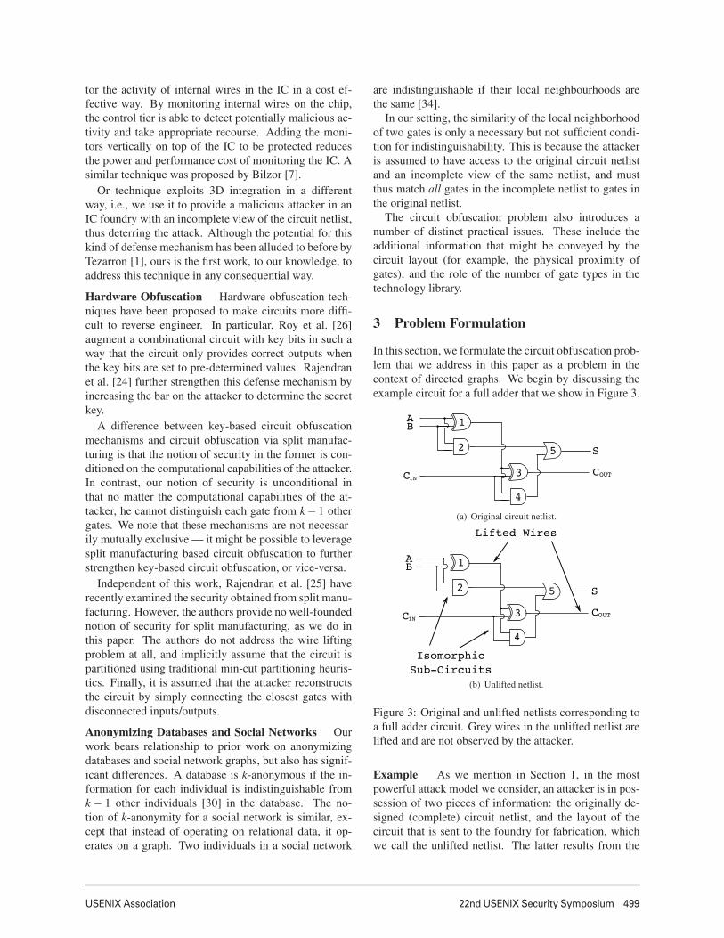
In this section, we formulate the circuit obfuscation prob-lem that we address in this paper as a problem in thecontext of directed graphs. We begin by discussing theexample circuit for a full adder that we show in Figure 3.
AB
CIN
S
COUT
1
2
3
4
5
(a) Original circuit netlist.
AB
CIN
S
COUT
Lifted Wires
IsomorphicSub-Circuits
1
2
3
4
5
(b) Unlifted netlist.
Figure 3: Original and unlifted netlists corresponding toa full adder circuit. Grey wires in the unlifted netlist arelifted and are not observed by the attacker.
Example As we mention in Section 1, in the mostpowerful attack model we consider, an attacker is in pos-session of two pieces of information: the originally de-signed (complete) circuit netlist, and the layout of thecircuit that is sent to the foundry for fabrication, whichwe call the unlifted netlist. The latter results from the
500 22nd USENIX Security Symposium USENIX Association
defender lifting wires from the former. Assume that thedefender chooses to lift the wires A→{1,2}, B→{1,2},CIN →{3,4}, 1 →{3,4} and 3 → COUT.
Note that gates in the unlifted netlist in Figure 3(b) arelabeled differently from those in the original circuit inFigure 3(a). This reflects the fact that the attacker ob-tains the original circuit netlist and the unlifted netlist incompletely different formats. The original netlist is a setof gates and wires in HDL format. On the other hand,the unlifted netlist is reconstructed from the circuit lay-out, which is a set of shapes and their locations on thesurface of the chip, as also discussed in Section 4.3. Thelabeling and ordering of objects in the circuit layout fileis unrelated to that in the netlist of the original circuit.Although not required, the defender can perform an ad-ditional random re-labeling and re-ordering step beforethe layout of H is sent to the foundry.
Given these two pieces of information, the attackernow seeks a bijective mapping of gates in the unliftednetlist to gates in the complete circuit netlist. If the at-tacker is successful in obtaining the correct mapping, hecan carry out a targeted attack on any gate (or gates) ofhis choosing. The security obtained from lifting wires inthe context of this example can be explained as follows.From the attacker’s perspective, either Gate u or Gate win the unlifted netlist could correspond to Gate 1 in theoriginal netlist. Thus the attacker’s ability to carry out atargeted attack on Gate 1 is hindered. The same can besaid for the attacker’s ability to carry out a targeted at-tack on Gate 2, 3 or 4. However, note that the attackercan determine the identity of Gate 5 with certainty — itmust correspond to Gate y since this is the only OR gatein the netlist. Thus, in this example, the lifting does notprovide any security for Gate 5.
Informally, our notion of security is based on the ex-istence of multiple isomorphisms (mappings) betweengates in the unlifted netlist and the original netlist. Inour example, there exist 4 distinct bijective mappings be-tween the gates in the unlifted and original netlists. How-ever, this notion of security may be seen as too permis-sive. It can be argued that given the fact that across allmappings, gate 5 is mapped uniquely, we have no secu-rity at all (i.e., security of 1). A more restrictive notionof security, one that we adopt in this paper, requires thatfor each gate in the original netlist, there exist at least kdifferent gates in the unlifted netlist that map to it overall isomorphisms. This is intended to capture the intu-ition that the attacker is unable to uniquely identify evena single gate. We now formalize our notion of security.
3.1 Formulation as a Graph Problem
We now formulate our problem as a graph problem. Acircuit can be perceived as a directed graph — gates are
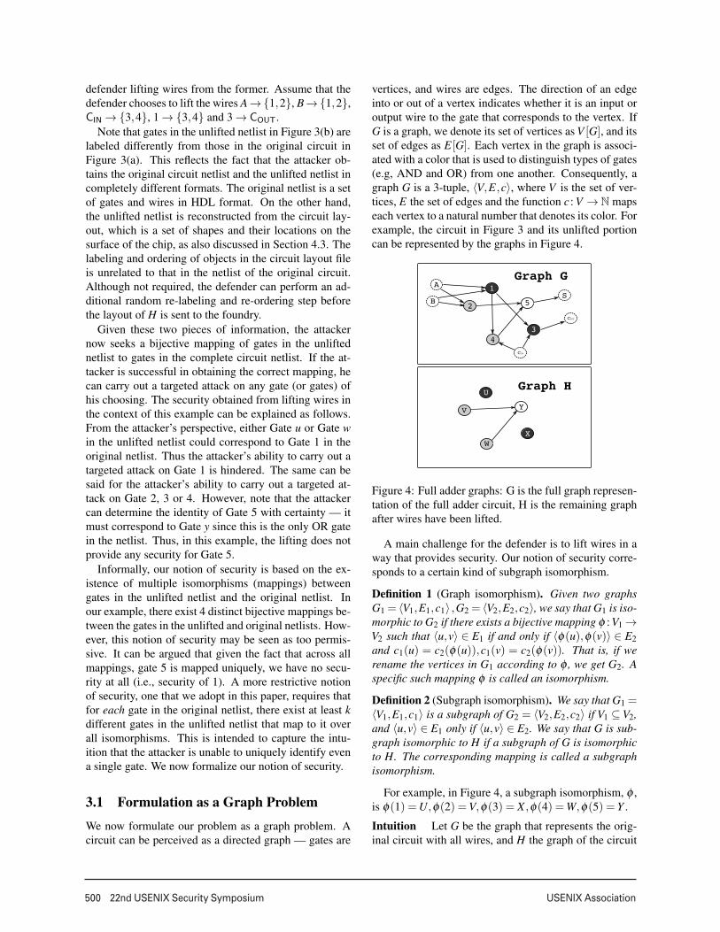
vertices, and wires are edges. The direction of an edgeinto or out of a vertex indicates whether it is an input oroutput wire to the gate that corresponds to the vertex. IfG is a graph, we denote its set of vertices as V [G], and itsset of edges as E[G]. Each vertex in the graph is associ-ated with a color that is used to distinguish types of gates(e.g, AND and OR) from one another. Consequently, agraph G is a 3-tuple, 〈V,E,c〉, where V is the set of ver-tices, E the set of edges and the function c : V →N mapseach vertex to a natural number that denotes its color. Forexample, the circuit in Figure 3 and its unlifted portioncan be represented by the graphs in Figure 4.
1
2
43
5S
COUT
CIN
A
B
U
V
WX
Y
Graph G
Graph H
Figure 4: Full adder graphs: G is the full graph represen-tation of the full adder circuit, H is the remaining graphafter wires have been lifted.
A main challenge for the defender is to lift wires in away that provides security. Our notion of security corre-sponds to a certain kind of subgraph isomorphism.
Definition 1 (Graph isomorphism). Given two graphsG1 = 〈V1,E1,c1〉 ,G2 = 〈V2,E2,c2〉, we say that G1 is iso-morphic to G2 if there exists a bijective mapping φ : V1 →V2 such that 〈u,v〉 ∈ E1 if and only if 〈φ(u),φ(v)〉 ∈ E2and c1(u) = c2(φ(u)),c1(v) = c2(φ(v)). That is, if werename the vertices in G1 according to φ , we get G2. Aspecific such mapping φ is called an isomorphism.
Definition 2 (Subgraph isomorphism). We say that G1 =〈V1,E1,c1〉 is a subgraph of G2 = 〈V2,E2,c2〉 if V1 ⊆V2,and 〈u,v〉 ∈ E1 only if 〈u,v〉 ∈ E2. We say that G is sub-graph isomorphic to H if a subgraph of G is isomorphicto H. The corresponding mapping is called a subgraphisomorphism.
For example, in Figure 4, a subgraph isomorphism, φ ,is φ(1) =U,φ(2) =V,φ(3) = X ,φ(4) =W,φ(5) = Y .
Intuition Let G be the graph that represents the orig-inal circuit with all wires, and H the graph of the circuit

USENIX Association 22nd USENIX Security Symposium 501
after wires have been lifted. Then, the attacker knowsthat G is subgraph isomorphic to H. What he seeks isthe correct mapping of vertices in G to H (or vice versa).This is equivalent to him having reconstructed the circuit,and now, he can effect his malicious modifications to thecircuit that corresponds to H.
From the defender’s standpoint, therefore, what weseek intuitively is that there be several subgraph isomor-phisms between G and H. As we mention in Section1, this then gives the kind of security in a k-anonymitysense — the attacker cannot be sure which of the map-pings is the correct one, and therefore is able to recon-struct the circuit with probability 1/k only. As we men-tion there and discuss in more detail in the related workSection, though our notion of security has similarities tok-anonymity, there are important differences, and we callit k-security instead.
k-security We now specify our notion of security. Wedo this in three stages. (1) We first define a problem thatcaptures our intuition of a gate being indistinguishablefrom another gate. We do this by requiring the existenceof a particular kind of subisomorphic mapping betweengraphs that represent circuits. (2) We then define thenotion of a k-secure gate. Such a gate is indistinguish-able from at least k − 1 other gates in the circuit. (3)Finally, we define the notion of k-security, which is secu-rity across all gates in the circuit. This definition requiressimply that every gate in the circuit is k-secure.
In the following definition, we characterize the prob-lem GATE-SUBISO, which captures (1) above — a notionof what it means for a gate to be indistinguishable fromanother.
Definition 3 (GATE-SUBISO). Given as input 〈G,E ′,u,v〉,where G is a DAG, E ′ ⊆ E[G], and two distinct verticesu,v ∈ V [G], let H be the graph we get by removing theedges that are in E ′ from G. Then, GATE-SUBISO is theproblem of determining whether there exists a mappingφ : V [G]→V [H] that is a subgraph isomorphism from Gto H such that φ(u) = v.
The above definition is a special case of the well-known subgraph isomorphism problem [16]. In the sub-graph isomorphism problem, we take as input two graphsA,B, and ask whether B is subgraph isomorphic to A. InGATE-SUBISO, both the graphs G,H are restricted to beDAGs, and H is a specific subgraph of G — one withsome edges removed from G. Of course, we know that His subgraph isomorphic to G, with the identity mappingfrom a vertex to itself serving as evidence (a certificate).However, in the GATE-SUBISO problem, we require the ex-istence of a subgraph isomorphism that is different fromthe identity mapping, and furthermore, require that thevertex u be mapped under that subgraph isomorphism toa specific vertex v.
The intuition behind GATE-SUBISO is the following. Gis the graph that corresponds to the original circuit, andH is the graph that corresponds to the circuit after wiresare lifted. The above definition for GATE-SUBISO askswhether there exists a mapping under which the vertexu in the original circuit is indistinguishable from v in theunlifted circuit. That is, given that u �= v, an attacker doesnot know whether u in G corresponds to u or v in H.
Based on GATE-SUBISO above, we now define the no-tion of a k-secure gate. It captures the intuition that thegate is indistinguishable from at least k−1 other gates.
Definition 4 (k-secure gate). Given a DAG, G, a vertexu in it, and a subgraph H of G constructed from G byremoving some edges, E ′ ⊆ E[G] only. We say that u isk-secure if there exist k distinct vertices v1, . . . ,vk in G(and therefore in H), and mappings φ1, . . . ,φk from V [G]to V [H] such that every φi is a subgraph isomorphismfrom G to H, and for all i ∈ [1,k], φi(u) = vi.
The above definition expresses that u is indistinguish-able from each of the vi’s. Of course, one of the vi’s maybe u itself. Therefore, every gate is 1-secure, and if a gateis not 2-secure, then that gate is uniquely identifiable, forthis particular choice of E ′. The maximum that k can beis |V [G]|, the number of a vertices in G.
Given the above definition for a k-secure gate, it is nowstraightforward to extend it to the entire graph (circuit).We do this with the following definition.
Definition 5 (k-security). Given a DAG G, and a DAGH that we get from G by removing the edges from a setE ′ ⊆ E[G]. We say that 〈G,E ′〉 is k-secure if every vertexin G is k-secure.
The above definition is a natural extension of the no-tion of a k-secure gate, to every gate in the circuit. Whatit requires for k-security is that every vertex in the corre-sponding graph is indistinguishable from at least k ver-tices. We point out that some gates may be more thank-secure; k-security is a minimum across all gates. Asthe maximum k for any gate is |V [G]|, a graph can be,at best, |V [G]|-secure. Every graph is 1-secure, which isthe minimum.
We denote as σ(G,E ′) the maximum k-security we areable to achieve with G,E ′. In Figure 4, for example, weknow that σ evaluates to 1, because the node 5 can bemapped to itself only. The nodes 1, 2, 3 and 4, however,are 2-secure gates. The reason is that each can be mappedeither to itself, or to another node.
Computational complexity We now consider thecomputational complexity of determining the maximumk-security, σ . We consider a corresponding decisionproblem, k-SECURITY-DEC, which is the following. Weare given as input 〈G,E ′,k〉 where G is a DAG, E ′ ⊆E[G]

502 22nd USENIX Security Symposium USENIX Association
is a set of edges in G, and k ∈ [1, |V [G]|]. The problemis to determine whether lifting the edges in E ′ results ink-security.
We point out that if we have an oracle that decidesk-SECURITY-DEC, then we can compute the maximum k-security we can get by lifting E ′ from G using binarysearch on k. That is, the problem of computing σ is easyif deciding k-SECURITY-DEC is easy.
Theorem 1. k-SECURITY-DEC ∈ NP-complete underpolynomial-time Turing reductions.
To prove the above theorem, we need to show thatk-SECURITY-DEC is in NP, and that it is NP-hard. For theformer, we need to present an efficiently (polynomial-sized) certificate that can be verified efficiently. Sucha certificate is k mappings each of which is a subgraphisomorphism, for each vertex u ∈V [G]. Each such map-ping can be encoded with size O(|V [G]|), and there areat most k|V [G]| such mappings, and therefore the certifi-cate is efficiently-sized. The verification algorithm sim-ply checks that each mapping is indeed a subgraph iso-morphism, and that u is mapped to a distinct vertex ineach of the k mappings that corresponds to it. This canbe done in time O(|V [G]|3).
We show that k-SECURITY-DEC is NP-hard un-der polynomial-time Turing reductions in the Ap-pendix. (Henceforth, we drop the qualification “un-der polynomial-time Turing reductions,” and simply sayNP-complete and NP-hard.) Indeed, our proof demon-strates that deciding even 2-security is NP-hard. Theknowledge that k-SECURITY-DEC is NP-complete imme-diately suggests techniques for approaches for solvingk-SECURITY-DEC, and thereby computing k-security. Wediscuss this further in the next section.
Choosing E ′ Lifting edges E ′ from G incurs a costc(G,E ′). A simple cost metric, one that we adopt inthis paper is c(G,E ′) = |E ′|, i.e., the cost is proportionalto the number of lifted edges. Given the cost of liftingedges, the defender’s goal is to determine E ′, the set ofedges that should be lifted, such that σ(G,E ′) ≥ k andc(G,E ′) is minimized.
We observe that from the standpoint of computationalcomplexity, the problem of determining E ′ given G,k,where G is the graph and E ′ is the set of edges to be liftedso we get k-security, is no harder than k-SECURITY-DEC.That is, that problem is also in NP.
To prove this, we need to show that there exists an ef-ficiently sized certificate that can be verified efficiently.Such a certificate is E ′, and k subgraph isomorphismsfor every vertex. The latter component of the certificateis the same as the one we used in our proof above fork-SECURITY-DEC’s membership in NP. The verificationalgorithm, in addition to doing what the verification al-
gorithm for k-SECURITY-DEC above does, also checks thatE ′ is indeed a subset of G’s edges.
We note that the k-security from lifting all the edgesin G is no worse than lifting any other set of edges, andthe k-security from lifting no edges in G is no better thanlifting any other set of edges. More generally, given anyn1,n2 such that |E[G]| ≥ n1 > n2, we know that for ev-ery G, there exists a set of edges of size n1 that if lifted,provides at least as much security as every set of edgesof size n2. That is, there is a natural trade-off betweenthe number of edges we lift, i.e., cost, and the securitywe achieve. In Section 4, we outline an approach to de-termine the cost-security trade-off using a greedy wirelifting procedure.
3.2 Discussion
Given our notion of k-security, a natural question to ask iswhether there are stronger or different attack models forwhich k-security would be inadequate. We discuss thisin the context of two attack models that differ from theone assumed. Finally, we also discuss a related question— that of the computational capabilities of the attacker.
General targeted attack models The notion of k-security is premised on an attack model in which the at-tacker needs to precisely identify one or more gates inthe unlifted netlist, for example, the privilege escalationbit in a microprocessor [19] or the LSB of the 14th roundin a DES implementation [9]. However, one can imaginea scenario in which the attack would be successful if theattacker correctly identifies any one of n gates. For ex-ample, there could be multiple privilege escalation bitsin the microprocessor implementation.
More concretely, in the example in Figure 3, assumethat the attacker wants to change the circuit functionalityby inverting the output of Gate 2. The same objectivecan be accomplished by inverting the output of Gate 4.However, as we observe before, Gate v in the unliftednetlist must correspond to either Gate 2 or Gate 4. Thus,although this gate is 2-secure, the attack would be suc-cessful with probability 1.
Although our notion of security does not directly ad-dress the alternate attack model described above, it canbe easily modified to do so. Say that the defender isaware that Gate v and Gate x are each equally vulnera-ble to the same kind of attack. Then, the defender caninsist that Gate v is k-secure if and only if it is indistin-guishable from k−1 other gates excluding Gate x. Suchinformation that the defender may have about the rela-tive vulnerability of gates can be built into the notion ofk-security.
Access to lifting procedure Our attack modelstrengthens the attacker with access to the original cir-

USENIX Association 22nd USENIX Security Symposium 503
cuit netlist, G, along with the unlifted netlist H. Sincethe attacker has access to G, it is reasonable to ask if aneven stronger attacker with access to G and the procedureused to lift wires would compromise security. It wouldnot.
1
Graph G
2 3 43 4 u
Graph H
x 3 4v w
Figure 5: Example illustrating that the unlifted netlist His 2-secure even if the attacker knows that edge 2 → 3was lifted from original netlist G.
In fact, even if there is a deterministic choice of edgesthat must be lifted to provide a certain security level,knowledge of which edges are lifted does not compro-mise security, as long as G and H are differently la-beled. We illustrate this with an example in Figure 5,where wire 2 → 3 must be lifted to provide 2-security.This knowledge does not compromise the security ob-tained from lifting. When there is choice, i.e., lifting twoor more edges provides the same security, the choice ismade uniformly at random. This is discussed in Sec-tion 4.
Computational capabilities of the attacker Our no-tion of k-security is not predicated on the computationalcapabilities of the attacker. In fact, we assume that theattacker is able to identify (all) subgraph isomorphismsfrom H to G. Nonetheless, given that the attacker’s goalmight be to identify a single gate in the netlist, it is natu-ral to ask why (and whether) the attacker needs determinea mapping for each gate in H.
In particular, the attacker can identify all gates in Hwith the same type and connectivity, i.e., number andtype of gates it connects to, as the one he is interested inattacking. Prior work on k-anonymity for social networkgraphs assumes this kind of attack strategy. From theperspective of the attacker, this strategy is sub-optimal.This is because, for any gate in G that the attacker wantsto target, this strategy will provide at least as many candi-date mappings in H as the strategy in which the attackerenumerates all subgraph isomorphisms.
4 Approach
Having considered the computational complexity of theproblem that underlies our work in the previous section,in this section, we propose a concrete approach for it.As our discussions in the prior section reveal, there aretwo parts to the solution: (a) computing the maximum
k-security for �G,E ��, given the graph G that representsthe complete circuit, and, (b) choosing the set E �.
We propose an approach for each in this section.For the problem of computing security, we employconstraint-solving. We discuss this in Section 4.1. Forthe problem of choosing E �, we propose a greedy heuris-tic. We discuss that in Section 4.2. We conclude thissection with Section 4.3 with some practical considera-tions, specifically, scalability and layout-anonymization.
4.1 Computing SecurityAs shown in Section 3, the problem of determining thesecurity level of circuit G, given the unlifted netlist His NP-complete. Given the relationship of the problemto subgraph isomorphism, a natural approach to solvingthis problem would be to use graph (sub)isomorphismalgorithms proposed in literature — of these, the VF2algorithm [12] has been empirically shown to be the mostpromising [15]. However, in our experience, VF2 doesnot scale for circuits with > 50 gates (more on scalabilityin Section 4.3).
Instead, motivated by the recent advances in thespeed and efficiency of SAT solvers, we reduce the sub-isomorphism problem to a SAT instance and use an off-the-shelf SAT solver to decide the instance.
Reduction to SAT Given graphs G and H, we de-fine a bijective mapping φ from the vertex set of H tothe vertex set of G as follows: Boolean variable φi jis true if and only if vertex qi ∈ H maps to a vertexr j ∈ G. Here V [G] = {r1,r2, . . . ,r|V [G]|} and V [H] ={q1,q2, . . . ,q|V [H]|}
We now construct a Boolean formula that is true if andonly if graphs G and H are sub-isomorphic for the map-ping φ . We will construct the formula in parts.
First, we ensure that each vertex in G maps to only onevertex in H:
F1 =|V [H]|∏
i
|V [G]|∑
j
(φi, j
|V [G]|∏k �=i
¬φi,k
)
and vice-versa:
F2 =|V [G]|∏
j
|V [H]|∑
i
(φi, j
|V [H]|∏k �=i
¬φk, j
)
Finally we need to ensure that each edge in Hmaps to an edge in G. Let E[H] = {e1,e2, . . . ,e|E[H]|}and E[G] = { f1, f2, . . . , f|E[G]|}. Furthermore, let ek =�qsrc(ek),qdest(ek)� ∈ E[H] and fk = �rsrc( fk),rdest( fk)� ∈E[G]. This condition can be expressed as follows:
F3 =|E[H]|∏
k
|E[G]|∑
lφsrc(ek),src( fl)∧φdest(ek),dest( fl)

504 22nd USENIX Security Symposium USENIX Association
The formula F that is input to the SAT solver is thenexpressed as a conjunction of the three formulae above:F = F1 ∧F2 ∧F3. The formula F has O(|V [H]||V [G]|)variables and O(|E[H]||E[G]|) clauses.
4.2 Wire Lifting ProcedureTo determine a candidate set of edges, E ′, to lift, we em-ploy a greedy heuristic. Our heuristic is shown as Algo-rithm 1.
1 E ′ ← E[G]2 while |E ′|> 0 do3 s ← 04 foreach e ∈ E ′ do5 E ′ ← E ′ −{e}6 if σ(G,E ′)> s then7 s ← σ(G,E ′)8 eb ← e9 E ′ ← E ′ ∪{e}
10 if s < k then return E ′
11 E ′ ← E ′ −{eb}12 return E ′
Algorithm 1: lift wires(G, k)
In our heuristic, we begin with the best security we canachieve. This occurs when we lift every edge in E[G];that is, we set E ′ to E[G] at the start in Line 1. We thenprogressively try to remove edges from E ′, in randomorder. We do this if not lifting a particular edge e stillgives us sufficient security.
That is, we iterate while we still have candidate edgesto add back (Line 2). If we do, we identify the “best”edge that we can add back, i.e., the one that gives us thegreatest security level if removed from E ′. If even thebest edge cannot be removed from E ′, then we are done(Line 10).
The heuristic does not necessarily yield an optimal setof edges. The reason is that we may greedily removean edge e1 from E ′ in an iteration of the above algo-rithm. And in later iterations, we may be unable to re-move edges e2 and e3. Whereas if we had left e1 in E ′,we may have been able to remove both e2 and e3. Notethat removing as many edges from E ′ is good, becauseour cost is monotonic in the size of E ′ (set of edges be-ing lifted).
4.3 Practical ConsiderationsFrom a graph-theoretic perspective, the wire lifting pro-cedure outlined provides a set of wires to lift that guaran-tees a certain security level. However, two practical con-siderations merit further mention — the scalability of the
proposed techniques to “large” circuits, and the securityimplication of the attacker having access to the layout ofH, as opposed to just the netlist.
Scalability Although the SAT based technique forcomputing security scales better than the VF2 algorithm,we empirically observe that it times out for circuits with> 1000 gates. To address this issue, we propose a circuitpartitioning approach that scales our technique to largercircuits of practical interest. We note that circuit parti-tioning is, in fact, a commonly used technique to addressthe scalability issue for a large number of automated cir-cuit design problems.
Algorithm 2 is a simplified description of the par-titioning based wire lifting procedure. The functionpartition(G) recursively partitions the vertex set of thegraph into P mutually exclusive subsets and returns sub-graphs {G1,G2, . . . ,GP} of size such that they can betractably solved by the SAT based greedy wire liftingprocedure. The final set of lifted wires includes the unionof all wires that cross partitions, and those returned byP calls to Algorithm 1. We have used this technique tolift wires from circuits with as many as 35000 gates (seeSection 5).
1 {G1,G2, . . . ,GP}← partition(G)2 ER ← E −
⋃
i∈[1,P] Ei
3 for i ∈ [1,P] do4 ER ← ER
⋃
li f t wires(Gi,sreq)5 return ER
Algorithm 2: lift wires big(G, sreq)
Layout anonymization We have, so far, assumed thatthe unlifted circuit H is a netlist corresponding to the un-lifted gates and wires. However, in practice, the attackerobserves a layout corresponding to H, from which he re-constructs the netlist of H. We therefore need to ensurethat the layout does not reveal any other information tothe attacker besides the reconstructed netlist.
Existing commercial layout tools place gates on thechip surface so as to minimize the average distance, typ-ically measured as the Manhattan distance, between allconnected gates in the circuit netlist. Thus, if the com-plete circuit G is used to place gates, the physical prox-imity of gates will reveal some information about liftedwires — gates that are closer in the bottom tier are morelikely to be connected in the top tier. The attacker canuse this information to his advantage.
Instead of using the netlist G to place gates, we insteaduse the netlist H. Since this netlist does not contain anylifted wires, these wires do not have any impact on theresulting placement. Conversely, we expect the physicalproximity of gates to reveal no information about hidden
USENIX Association 22nd USENIX Security Symposium 505
wires in the top tier. In Section 5, we empirically validatethis fact. However, anonymizing the layout with respectto the hidden wires does result in increased wire-lengthbetween gates, which has an impact on circuit perfor-mance. This impact is also quantified in Section 5.
5 Results
We conduct our experimental study using two exemplarbenchmarks, the c432 circuit from the ISCAS-85 bench-mark suite [10] (a 27-channel bus interrupt controller)with ≈ 200 gates, and a larger DES encryption circuitwith ≈ 35000 gates. We use the c432 circuit to investi-gate security-cost trade-offs obtained from the proposedtechniques and use the larger DES circuit for a casestudy.
All experimental results are obtained using an IBM0.13µ technology. For 3D integration, bond points areassumed to be spaced at a pitch of 4µm, allowing for onebond-point per 16µm2. This is consistent with the designrules specified in the Tezzaron 0.13µm technology kit.
Circuit synthesis was performed using the BerkeleySIS tool [27]. Placement and routing is performed us-ing Cadence Encounter. Finally, we used miniSAT asour SAT solver [29].
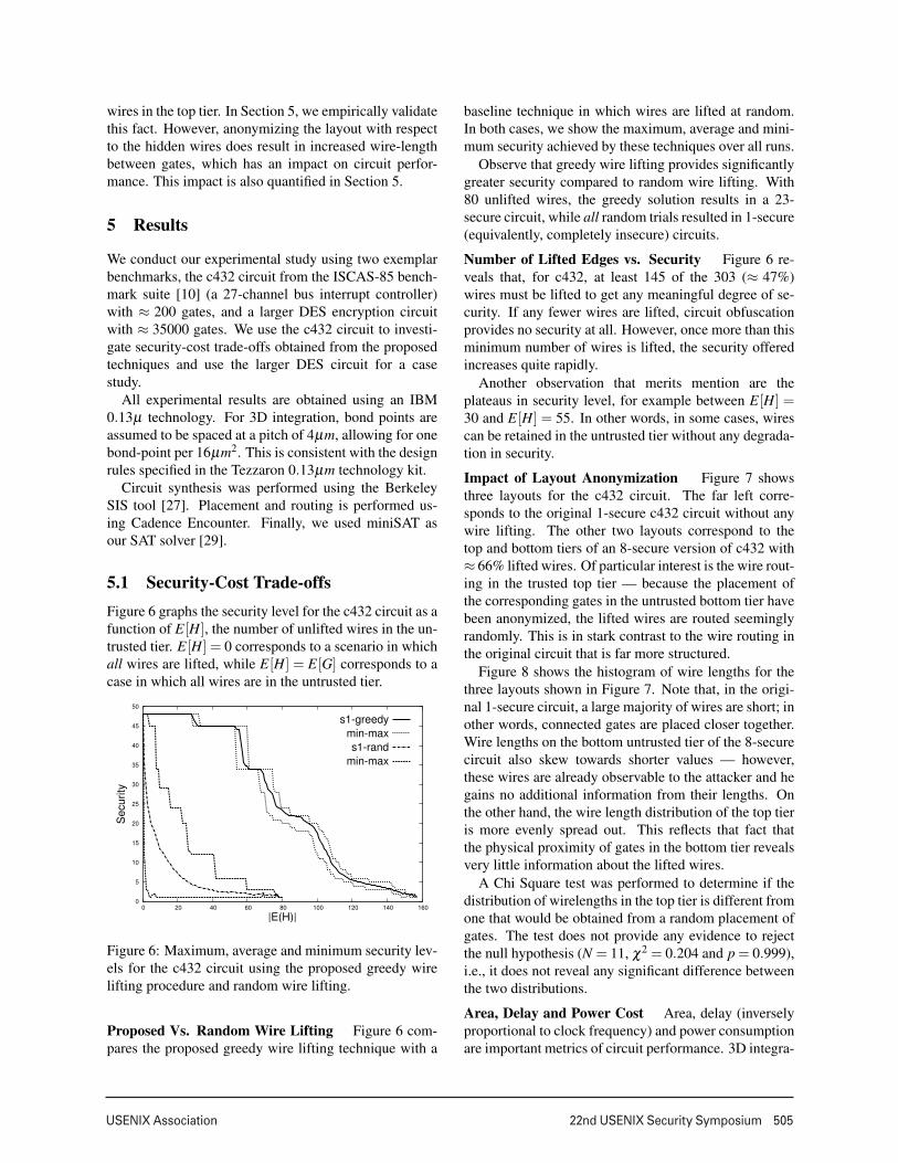
5.1 Security-Cost Trade-offsFigure 6 graphs the security level for the c432 circuit as afunction of E[H], the number of unlifted wires in the un-trusted tier. E[H] = 0 corresponds to a scenario in whichall wires are lifted, while E[H] = E[G] corresponds to acase in which all wires are in the untrusted tier.
0
5
10
15
20
25
30
35
40
45
50
0 20 40 60 80 100 120 140 160
Sec
urity
|E(H)|
s1-greedymin-maxs1-rand
min-max
Figure 6: Maximum, average and minimum security lev-els for the c432 circuit using the proposed greedy wirelifting procedure and random wire lifting.
Proposed Vs. Random Wire Lifting Figure 6 com-pares the proposed greedy wire lifting technique with a
baseline technique in which wires are lifted at random.In both cases, we show the maximum, average and mini-mum security achieved by these techniques over all runs.
Observe that greedy wire lifting provides significantlygreater security compared to random wire lifting. With80 unlifted wires, the greedy solution results in a 23-secure circuit, while all random trials resulted in 1-secure(equivalently, completely insecure) circuits.
Number of Lifted Edges vs. Security Figure 6 re-veals that, for c432, at least 145 of the 303 (≈ 47%)wires must be lifted to get any meaningful degree of se-curity. If any fewer wires are lifted, circuit obfuscationprovides no security at all. However, once more than thisminimum number of wires is lifted, the security offeredincreases quite rapidly.
Another observation that merits mention are theplateaus in security level, for example between E[H] =30 and E[H] = 55. In other words, in some cases, wirescan be retained in the untrusted tier without any degrada-tion in security.
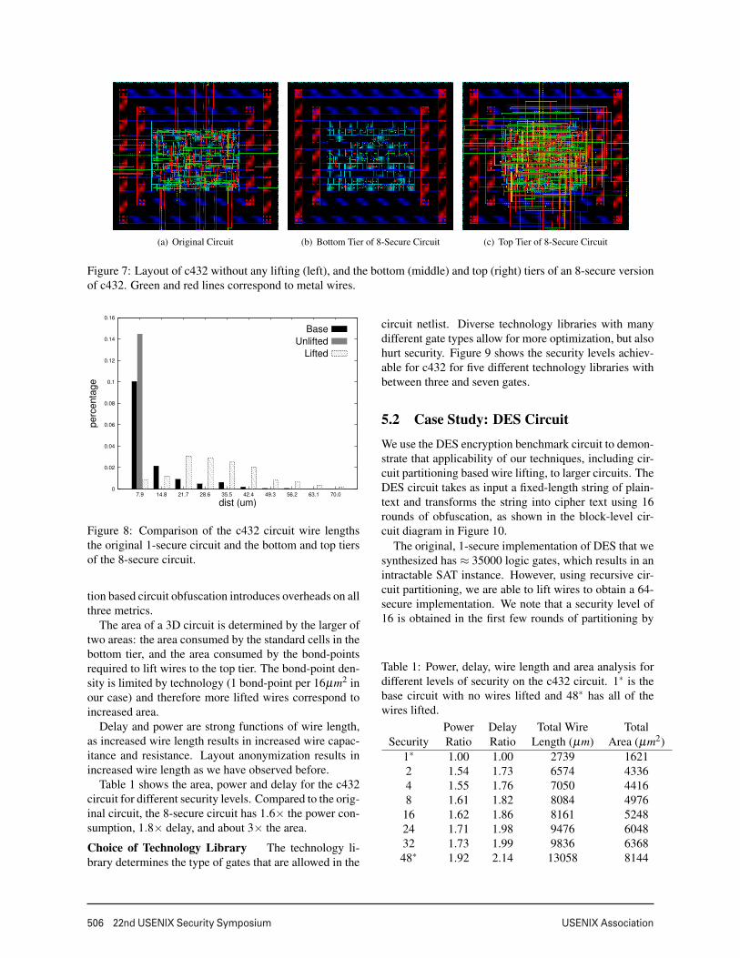
Impact of Layout Anonymization Figure 7 showsthree layouts for the c432 circuit. The far left corre-sponds to the original 1-secure c432 circuit without anywire lifting. The other two layouts correspond to thetop and bottom tiers of an 8-secure version of c432 with≈ 66% lifted wires. Of particular interest is the wire rout-ing in the trusted top tier — because the placement ofthe corresponding gates in the untrusted bottom tier havebeen anonymized, the lifted wires are routed seeminglyrandomly. This is in stark contrast to the wire routing inthe original circuit that is far more structured.
Figure 8 shows the histogram of wire lengths for thethree layouts shown in Figure 7. Note that, in the origi-nal 1-secure circuit, a large majority of wires are short; inother words, connected gates are placed closer together.Wire lengths on the bottom untrusted tier of the 8-securecircuit also skew towards shorter values — however,these wires are already observable to the attacker and hegains no additional information from their lengths. Onthe other hand, the wire length distribution of the top tieris more evenly spread out. This reflects that fact thatthe physical proximity of gates in the bottom tier revealsvery little information about the lifted wires.
A Chi Square test was performed to determine if thedistribution of wirelengths in the top tier is different fromone that would be obtained from a random placement ofgates. The test does not provide any evidence to rejectthe null hypothesis (N = 11, χ2 = 0.204 and p = 0.999),i.e., it does not reveal any significant difference betweenthe two distributions.
Area, Delay and Power Cost Area, delay (inverselyproportional to clock frequency) and power consumptionare important metrics of circuit performance. 3D integra-
506 22nd USENIX Security Symposium USENIX Association
(a) Original Circuit (b) Bottom Tier of 8-Secure Circuit (c) Top Tier of 8-Secure Circuit
Figure 7: Layout of c432 without any lifting (left), and the bottom (middle) and top (right) tiers of an 8-secure versionof c432. Green and red lines correspond to metal wires.
0
0.02
0.04
0.06
0.08
0.1
0.12
0.14
0.16
7.9 14.8 21.7 28.6 35.5 42.4 49.3 56.2 63.1 70.0
perc
enta
ge
dist (um)
BaseUnlifted
Lifted
Figure 8: Comparison of the c432 circuit wire lengthsthe original 1-secure circuit and the bottom and top tiersof the 8-secure circuit.
tion based circuit obfuscation introduces overheads on allthree metrics.
The area of a 3D circuit is determined by the larger oftwo areas: the area consumed by the standard cells in thebottom tier, and the area consumed by the bond-pointsrequired to lift wires to the top tier. The bond-point den-sity is limited by technology (1 bond-point per 16µm2 inour case) and therefore more lifted wires correspond toincreased area.
Delay and power are strong functions of wire length,as increased wire length results in increased wire capac-itance and resistance. Layout anonymization results inincreased wire length as we have observed before.
Table 1 shows the area, power and delay for the c432circuit for different security levels. Compared to the orig-inal circuit, the 8-secure circuit has 1.6× the power con-sumption, 1.8× delay, and about 3× the area.
Choice of Technology Library The technology li-brary determines the type of gates that are allowed in the
circuit netlist. Diverse technology libraries with manydifferent gate types allow for more optimization, but alsohurt security. Figure 9 shows the security levels achiev-able for c432 for five different technology libraries withbetween three and seven gates.
5.2 Case Study: DES Circuit
We use the DES encryption benchmark circuit to demon-strate that applicability of our techniques, including cir-cuit partitioning based wire lifting, to larger circuits. TheDES circuit takes as input a fixed-length string of plain-text and transforms the string into cipher text using 16rounds of obfuscation, as shown in the block-level cir-cuit diagram in Figure 10.
The original, 1-secure implementation of DES that wesynthesized has ≈ 35000 logic gates, which results in anintractable SAT instance. However, using recursive cir-cuit partitioning, we are able to lift wires to obtain a 64-secure implementation. We note that a security level of16 is obtained in the first few rounds of partitioning by
Table 1: Power, delay, wire length and area analysis fordifferent levels of security on the c432 circuit. 1∗ is thebase circuit with no wires lifted and 48∗ has all of thewires lifted.
Power Delay Total Wire TotalSecurity Ratio Ratio Length (µm) Area (µm2)
1∗ 1.00 1.00 2739 16212 1.54 1.73 6574 43364 1.55 1.76 7050 44168 1.61 1.82 8084 4976
16 1.62 1.86 8161 524824 1.71 1.98 9476 604832 1.73 1.99 9836 636848∗ 1.92 2.14 13058 8144

USENIX Association 22nd USENIX Security Symposium 507
Table 2: Technology libraries used for the experiment inFigure 9. lib-x corresponds to a library with x differentgate types.
Library max(S1) |V (G)| |E(G)| Gateslib-3 48 209 303 inv, nor, nandlib-4 24 181 271 +nand 3lib-5 13 169 259 +nor 3lib-6 7 165 252 +nand 4lib-7 4 159 246 +nor 4
0
5
10
15
20
25
30
35
40
45
50
0 20 40 60 80 100 120 140 160
Sec
urity
|E(H)|
lib-3lib-4lib-5lib-6lib-7
Figure 9: Obtainable security levels for the c432 circuitwith different technology libraries.
removing only 13% of the wires, i.e., all wires that liebetween successive DES rounds. This is because the cir-cuit description of each DES round is identical — thus,once the wires between the rounds have been removed,each round can be confused for any other round. The fi-nal 64-secure implementation has only 30% of the wiresunlifted, and consumes 2.38× the area of the original 1-secure circuit.
Attack Scenario Boneh et al. [9] have shown that spe-cific bits in a DES implementation are particularly sus-ceptible to fault attacks. For example, if the attacker isable to insert an attack such that the LSB output of the14th round is stuck at logic zero, the secret key can berecovered using as few as two messages.
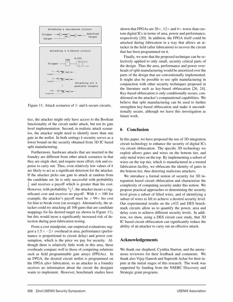
Figure 11 shows how such an attack might be effectedusing a trigger (we do not address here how this triggermay be activated) and three additional gates in an inse-cure (or 1-secure) circuit. When the trigger is set, the out-put is set to zero, but is equal to the correct value whenthe trigger is at logic zero.
Now, assume that wire lifting is performed to make thecircuit 64-secure. Given the set of lifted wires, we notethat the LSB of the 14th round is, in fact, 256-secure, i.e.,there are 255 other gates in the circuit that are indistin-guishable from the LSB of the 14th round.
Plaintext
Round 01
Round 14
IP
FB
Round 16
Ciphertext
Round 15
Figure 10: Block diagram of the DES encryption circuit.
The attacker now has two choices. he can either attackone of the 256 options, and only succeed with probabil-ity 1
256 , or he can choose to carry out a multiplexed attackon all 256 gates. This is shown in Figure 11. In this at-tack, the trigger transmits a sequence of 8-bits that iden-tify which of the 256 signals the attacker wants to attack.These 8-bits feed an 8:256 demultiplexer that generatesindividual triggers for each of the 256 signals that areindistinguishable.
The attacker can now iteratively insert attacks in eachgate one at a time and conceivably determine which iter-ation actually corresponds to the LSB of the 14th round.However, in doing so, the attacker incurs two costs: (i)the modified attack circuit now requires 1280 gates in-stead of just 3, a 420× overhead; (ii) the attacker wouldrequire, in the worst case 255× more messages to re-cover the key.
5.3 Discussion
We have so far illustrated the quantitative trade-off be-tween cost and security using benchmark circuits. Wenow discuss this trade-off qualitatively. In particular, weaddress aspects relating to both the security that 3D ICbased split manufacturing can provide and the cost that itincurs in doing so.
From a security standpoint, we note that our notion ofk-security is conservative. This is for two reasons. First,we have assumed a strong attack model in which the at-tacker has access to the original circuit netlist. In prac-
508 22nd USENIX Security Symposium USENIX Association
ModifiedTarget
Target
Trigger
8:256t1
t255
t2
FSM
Trigger
Attacking a non-secure circuit
target1
t1
Attacking a k-secure circuit
target2
t2
target255
t255
Attacking all kpossible targets
Figure 11: Attack scenarios of 1- and k-secure circuits.
tice, the attacker might only have access to the Booleanfunctionality of the circuit under attack, but not its gatelevel implementation. Second, in realistic attack scenar-ios, the attacker might need to identify more than onegate in the netlist. In both settings k-security serves as alower bound on the security obtained from 3D IC basedsplit manufacturing.
Furthermore, hardware attacks that are inserted in thefoundry are different from other attack scenarios in thatthey are single shot, and require more effort, risk and ex-pense to carry out. Thus, even relatively low values of kare likely to act as a significant deterrent for the attacker.If the attacker picks one gate to attack at random fromthe candidate set, he is only successful with probability1k and receives a payoff which is greater than his cost.However, with probability k−1
k , the attacker incurs a (sig-nificant) cost and receives no payoff. With k = 100 forexample, the attacker’s payoff must be > 99× his costfor him to break even (on average). Alternatively, the at-tacker could try attacking all 100 gates that are candidatemappings for his desired target (as shown in Figure 11),but this would incur a significantly increased risk of de-tection during post-fabrication testing.
From a cost standpoint, our empirical evaluations sug-gest a 1.5×−2× overhead in area, performance (perfor-mance is proportional to circuit delay) and power con-sumption, which is the price we pay for security. Al-though there is relatively little work in this area, theseoverheads compare well to those of competing solutionssuch as field programmable gate arrays (FPGAs). Inan FPGA, the desired circuit netlist is programmed onthe FPGA after fabrication, so an attacker in a foundryreceives no information about the circuit the designerwants to implement. However, benchmark studies have
shown that FPGAs are 20×, 12× and 4× worse than cus-tom digital ICs in terms of area, power and performance,respectively [20]. In addition, the FPGA itself could beattacked during fabrication in a way that allows an at-tacker in the field (after fabrication) to recover the circuitthat has been programmed on it.
Finally, we note that the proposed technique can be se-lectively applied to only small, security critical parts ofthe design. Thus the area, performance and power over-heads of split manufacturing would be amortized over theparts of the design that are conventionally implemented.It might also be possible to use split manufacturing inconjunction with other security techniques proposed inthe literature such as key-based obfuscation [26, 24].Key-based obfuscation is only conditionally secure, con-ditioned on the attacker’s computational capabilities. Webelieve that split manufacturing can be used to furtherstrengthen key-based obfuscation and make it uncondi-tionally secure, although we leave this investigation asfuture work.
6 Conclusion
In this paper, we have proposed the use of 3D integrationcircuit technology to enhance the security of digital ICsvia circuit obfuscation. The specific 3D technology weexploit allows gates and wires on the bottom tier, andonly metal wires on the top. By implementing a subset ofwires on the top tier, which is manufactured in a trustedfabrication facility, we obfuscate the identity of gates inthe bottom tier, thus deterring malicious attackers.
We introduce a formal notion of security for 3D in-tegration based circuit obfuscation and characterize thecomplexity of computing security under this notion. Wepropose practical approaches to determining the securitylevel given a subset of lifted wires, and of identifying asubset of wires to lift to achieve a desired security level.Our experimental results on the c432 and DES bench-mark circuits allow us to quantify the power, area anddelay costs to achieve different security levels. In addi-tion, we show, using a DES circuit case study, that 3DIC based circuit obfuscation can significantly reduce theability of an attacker to carry out an effective attack.
Acknowledgements
We thank our shepherd, Cynthia Sturton, and the anony-mous reviewers for their feedback and comments. Wethank also Vijay Ganesh and Supreeth Achar for their in-puts at the initial stages of this research. The work wassupported by funding from the NSERC Discovery andStrategic grant programs.
USENIX Association 22nd USENIX Security Symposium 509
References[1] 3D-ICs and Integrated Circuit Security. Tech. rep., Tezzarron
Semiconductors, 2008.
[2] ADEE, S. The hunt for the kill switch. IEEE Spectrum 45, 5(may 2008), 34 –39.
[3] AGRAWAL, D., BAKTIR, S., KARAKOYUNLU, D., ROHATGI,P., AND SUNAR, B. Trojan detection using IC fingerprinting.In Proceedings of the IEEE Symposium on Security and Privacy(2007), IEEE, pp. 296–310.
[4] ALKABANI, Y., AND KOUSHANFAR, F. N-variant IC design:Methodology and applications. In Proceedings of the 45th annualDesign Automation Conference (2008), ACM, pp. 546–551.
[5] ARORA, S., AND BARAK, B. Computational Complexity: AModern Approach. Cambridge University Press, 2009.
[6] BANERJEE, K., SOURI, S. J., KAPUR, P., AND SARASWAT,K. C. 3-D ICs: A novel chip design for improving deep-submicrometer interconnect performance and systems-on-chipintegration. Proceedings of the IEEE 89, 5 (2001), 602–633.
[7] BILZOR, M. 3D execution monitor (3D-EM): Using 3D circuitsto detect hardware malicious inclusions in general purpose pro-cessors. In Proceedings of the 6th International Conference onInformation Warfare and Security (2011), Academic ConferencesLimited, p. 288.
[8] BOLSENS, I. 2.5D ICs: Just a stepping stone or a long termalternative to 3D? In Keynote Talk at 3-D Architectures for Semi-conductor Integration and Packaging Conference (2011).
[9] BONEH, D., DEMILLO, R., AND LIPTON, R. On the importanceof checking cryptographic protocols for faults. In Advances inCryptology – EUROCRYPT (1997), Springer, pp. 37–51.
[10] BRGLEZ, F. Neutral netlist of ten combinational benchmark cir-cuits and a target translator in fortran. In Special session onATPG and fault simulation, Proc. IEEE International Symposiumon Circuits and Systems, June 1985 (1985), pp. 663–698.
[11] CHAKRABORTY, R. S., NARASIMHAN, S., AND BHUNIA, S.Hardware trojan: Threats and emerging solutions. In Proceed-ings of the IEEE International Workshop on High Level DesignValidation and Test (HLDVT) (2009), IEEE, pp. 166–171.
[12] CORDELLA, L. P., FOGGIA, P., SANSONE, C., AND VENTO,M. Performance evaluation of the vf graph matching algorithm.In Proceedings of the International Conference on Image Analy-sis and Processing (1999), IEEE, pp. 1172–1177.
[13] DAVIS, W. R., WILSON, J., MICK, S., XU, J., HUA, H., MI-NEO, C., SULE, A. M., STEER, M., AND FRANZON, P. D. De-mystifying 3D ICs: the pros and cons of going vertical. Design& Test of Computers, IEEE 22, 6 (2005), 498–510.
[14] DENG, Y., AND MALY, W. 2.5 D system integration: a de-sign driven system implementation schema. In Proceedings ofthe Asia and South Pacific Design Automation Conference (ASP-DAC) (2004), IEEE, pp. 450–455.
[15] FOGGIA, P., SANSONE, C., AND VENTO, M. A performancecomparison of five algorithms for graph isomorphism. In Pro-ceedings of the 3rd IAPR TC-15 Workshop on Graph-based Rep-resentations in Pattern Recognition (2001), pp. 188–199.
[16] GARY, M., AND JOHNSON, D. Computers and intractability: Aguide to the theory of np-completeness, 1979.
[17] HICKS, M., FINNICUM, M., KING, S. T., MARTIN, M. M.,AND SMITH, J. M. Overcoming an untrusted computing base:Detecting and removing malicious hardware automatically. InProceedings of the IEEE Symposium on Security and Privacy(2010), IEEE, pp. 159–172.
[18] IRVINE, C. E., AND LEVITT, K. Trusted hardware: Can it betrustworthy? In Proceedings of the 44th Annual Design Automa-tion Conference (2007), ACM, pp. 1–4.
[19] KING, S., TUCEK, J., COZZIE, A., GRIER, C., JIANG, W.,AND ZHOU, Y. Designing and implementing malicious hard-ware. In Proceedings of the 1st USENIX Workshop on Large-scale Exploits and Emergent Threats (2008), USENIX Associa-tion, pp. 1–8.
[20] KUON, I., AND ROSE, J. Measuring the gap between fpgas andasics. In Proceedings of the 2006 ACM/SIGDA 14th internationalSymposium on Field programmable gate arrays (2006), ACM,pp. 21–30.
[21] LAU, J. H. TSV interposer: The most cost-effective integratorfor 3D IC integration. Chip Scale Review (2011), 23–27.
[22] MICCIANCIO, D., AND GOLDWASSER, S. Complexity of Lat-tice Problems: a cryptographic perspective, vol. 671 of TheKluwer International Series in Engineering and Computer Sci-ence. Kluwer Academic Publishers, Boston, Massachusetts, Mar.2002.
[23] MICROSEMI. Microsemi ProASIC3 FPGA security overview,2012. Available from www.microsemi.com/documents/.
[24] RAJENDRAN, J., PINO, Y., SINANOGLU, O., AND KARRI, R.Security analysis of logic obfuscation. In Proceedings of the 49thAnnual Design Automation Conference (2012), ACM, pp. 83–89.
[25] RAJENDRAN, J., SINANOGLU, O., AND KARRI, R. Is split man-ufacturing secure? In Proceedings of the Design, Automation &Test in Europe Conference & Exhibition (DATE) (2013), IEEE,pp. 1259–1264.
[26] ROY, J. A., KOUSHANFAR, F., AND MARKOV, I. L. Epic: End-ing piracy of integrated circuits. In Proceedings of the confer-ence on Design, Automation and Test in Europe (2008), ACM,pp. 1069–1074.
[27] SENTOVICH, E. M., SINGH, K. J., MOON, C., SAVOJ, H.,BRAYTON, R. K., AND SANGIOVANNI-VINCENTELLI, A. Se-quential circuit design using synthesis and optimization. In Pro-ceedings of the IEEE International Conference on Computer De-sign (ICCD) (1992), IEEE, pp. 328–333.
[28] SKOROBOGATOV, S., AND WOODS, C. Breakthrough siliconscanning discovers backdoor in military chip. CryptographicHardware and Embedded Systems–CHES (2012), 23–40.
[29] SORENSSON, N., AND EEN, N. Minisat v1. 13-a sat solver withconflict-clause minimization. SAT 2005 (2005), 53.
[30] SWEENEY, L. k-anonymity: A model for protecting privacy.International Journal of Uncertainty, Fuzziness and Knowledge-Based Systems 10, 05 (2002), 557–570.
[31] TEHRANIPOOR, M., AND KOUSHANFAR, F. A survey of hard-ware trojan taxonomy and detection. Design & Test of Comput-ers, IEEE 27, 1 (2010), 10–25.
[32] VALAMEHR, J., TIWARI, M., SHERWOOD, T., KASTNER, R.,HUFFMIRE, T., IRVINE, C., AND LEVIN, T. Hardware as-sistance for trustworthy systems through 3-D integration. InProceedings of the 26th Annual Computer Security ApplicationsConference (2010), ACM, pp. 199–210.
[33] WAKSMAN, A., AND SETHUMADHAVAN, S. Silencing hard-ware backdoors. In Proceedings of the IEEE Symposium on Se-curity and Privacy (2011), IEEE, pp. 49–63.
[34] ZHOU, B., AND PEI, J. Preserving privacy in social networksagainst neighborhood attacks. In Proceedings of the 24th IEEEInternational Conference on Data Engineering (ICDE) (2008),IEEE, pp. 506–515.
510 22nd USENIX Security Symposium USENIX Association
A k-SECURITY-DEC is NP-hard
In this section, we provide outlines of the proofs that un-derlie our assertion in Section 3 that k-SECURITY-DEC isNP-hard under polynomial-time Turing, or Cook, reduc-tions [5]. Such reductions work the following way. Sup-pose we want to reduce problem A to B. We show that ifwe have an oracle for B, then A ∈ P.
Such reductions are unlikely to be as strong as Karp-reductions [5], that are customarily used to show NP-hardness. Indeed, the Karp-reduction is a special caseof the Cook-reduction, and some of our reductions be-low are Karp-reductions. Nevertheless, the existence ofa Cook-reduction from a problem that is NP-hard is ev-idence of intractability [22]. In particular, in the aboveexample, if A reduces to B, then if B ∈ P, then A ∈ P.
Recall from Section 3 that k-SECURITY-DEC is the fol-lowing decision problem. Given as input 〈G,E ′,k〉where E ′ ⊆ E[G], does lifting the edges in E ′ give usk-security? We show that k-SECURITY-DEC is NP-hardin three steps. First, we show that SUB-ISO-SELF (de-fined below) is NP-hard. We then reduce SUB-ISO-SELF
to GATE-SUBISO (see Section 3), thereby showing thatGATE-SUBISO is NP-hard. Finally, we reduce GATE-SUBISO
to k-SECURITY-DEC.All graphs we consider are directed, acyclic (DAGs).
Thus, all subisomorphisms we consider are for the spe-cial case that the graphs are DAGs. It turns out that thesubgraph isomorphism problem is NP-hard for even therestricted case, SUB-ISO-9, below.
Definition 6 (SUB-ISO-9). SUB-ISO-9 is the following spe-cial case of the subgraph isomorphism problem. Givenas input 〈G,H〉 where G is a DAG and H is a directedtree, SUB-ISO-9 is the problem of determining whetherthere exists a subgraph of G that is isomorphic to H.
SUB-ISO-9 is known to be NP-hard [16].
Definition 7 (SUB-ISO-SELF). Given as input 〈G,H〉 suchthat G is a DAG and H is obtained from G by removingthe edges in a set E ′ ⊆ E[G], SUB-ISO-SELF is the problemof determining whether there exists a subgraph isomor-phism φ from G to H that is not the identity mapping.
Theorem 2. SUB-ISO-SELF ∈ NP-hard.
Note that the above theorem is not qualified that it isunder Cook-reductions. This is because we have a Karp-reduction from SUB-ISO-9 ro SUB-ISO-SELF. The reductionproceeds in several steps. First, we show that SUB-ISO-9restricted to the case that |V [G]|= |V [H]| leaves the prob-lem NP-hard. We do this by first observing that for anyprospective instance 〈G,H〉 of SUB-ISO-9, we can assumethat |V [H]| ≤ |V [G]|. We simply add |V [G]|−|V [H]| ver-tices to H.
Then, we show that if we add the further restrictionthat G and H are strongly connected (i.e., every vertexreachable from every other vertex), the problem is stillNP-hard. For this reduction, we first check whether thetwo graphs are strong connected. If not, we introduce anew vertex of a colour distinct from every vertex in thegraphs which has an edge to and from every other vertex.
We then show that SUB-ISO-SELF is NP-hard as follows.We introduce into G an exact copy of H that is disjointfrom G. We call this new graph G′, and the subgraphof G′ that is the copy of H, H ′. We further restrict Hand H ′ to not have any automorphisms. To achieve this,we introduce |V [H]| vertices each of a distinct colour,associated with each u ∈ V [H]. Call this vertex vu. Weconnect u and vu with an edge. We do the same in H ′. Wealso add a subgraph G′′ to H which has |V [G]| verticesand no edges. (This guarantees that the new subgraph issubgraph isomorphic to G.) We call this new graph H ′′.
We use the same technique as above of addingcoloured vertices to ensure that G (within G′) and G′′ inH ′′ are not automorphic. Finally, we connect every newvertex added above to the vertices of G, to every originalvertex of H ′, and every new vertex added to H ′ to everyoriginal vertex of G. We do the same in H ′′. We now areable to show that 〈G,H〉 is a true instance of SUB-ISO-9 ifand only if 〈G′,H ′′〉 is an instance of SUB-ISO-SELF.
Theorem 3. GATE-SUBISO ∈ NP-hard under Cook-reductions.
Recall that GATE-SUBISO comprises those instances〈G,E ′,u,v〉, where, if H is produced from G by remov-ing the edges in E ′, and u,v are distinct vertices in G (andtherefore H), there is a subgraph isomorphism from G toH that maps u to v. In our reduction, we assume that wehave an oracle for GATE-SUBISO. We simply invoke it forevery pair of vertices u,v ∈ G. If any of them is true, thenwe know that 〈G,H〉 is a true instance of SUB-ISO-SELF.Otherwise, it is not.
Theorem 4. k-SECURITY-DEC ∈ NP-hard under Cook-reductions.
We Karp-reduce GATE-SUBISO to k-SECURITY-DEC. Let〈G,E ′,k〉 be a prospective instance of k-SECURITY-DEC,and H is produced from G by removing the edges in E ′.We first ensure that every vertex other than u is 2-secure.We do this by introduce a new vertex for every vertexother than u that has exactly the same connectivity. Then,in G, we introduce a new vertex of a completely newcolour and attach it to u and v. We include the edge be-tween v and this new vertex in E ′. Call the G so modifiedG′′, and the new set of edges E ′′. We can now show that〈G′′,E ′′,2〉 is a true instance of k-SECURITY-DEC if andonly if 〈G,E ′,u,v〉 is a true instance of GATE-SUBISO.
Related Documents


![Hardware Trojan: Threats and Emerging Solutionsswarup.ece.ufl.edu/papers/IC/IC6.pdf · tive de-packaging and reverse-engineering of the IC [3], or Fig. 1. Vulnerable steps of a modern](https://static.cupdf.com/doc/110x72/5e62e4e4cc371f60e134e178/hardware-trojan-threats-and-emerging-tive-de-packaging-and-reverse-engineering.jpg)