SUBJECT: ‘COMPUTER SYSTEM ARCHITECTURE (BCA-4) Page 1 of 72 Note: This question-bank contains three sections. Section-A contains 1 mark Multiple Choice Objective type questions. Section-B contains 5 marks subjective questions. Section-A contains 10 marks subjective questions. Section – A 1 Mark Questions MULTIPLE CHOICE OBJECTIVE TYPE QUESTION Multiple-choice questions: 1. For converting Assembly language to machine-language, we need: a. Compiler b. Interpreter c. Assembler d. Program can be directly executed Answer: c 2. The decimal number 12 is represented respectively in hexadecimal and octal as: a: C,14 b: 14,C c: C,12 d: B,14 Answer: a 3. The subtraction of binary number 1000100 from 1010100 will give the result: a: 10010000 b: 0010000 c: 10001111 d: 0001000 Answer: b 4: BCD representation for binary number 543 is: a: 10101000011 b: 010100110100 c: 010101000011 d: 101100011 Answer: c 5: Which out of the following is a universal gate: a: X-OR b: X-NOR c: NOR d: None of the above Answer: c 6: The algebraic output expression of which of the following gates is A’B + AB’ a: NOR Prepared By: - Vaishnoo Maa Computers, SCO 145, Chotti Baradari, Patiala. Ph. 0175-2205100, 2215100

Welcome message from author
This document is posted to help you gain knowledge. Please leave a comment to let me know what you think about it! Share it to your friends and learn new things together.
Transcript

SUBJECT: ‘COMPUTER SYSTEM ARCHITECTURE (BCA-4) Page 1 of 57
Note: This question-bank contains three sections.Section-A contains 1 mark Multiple Choice Objective type questions.Section-B contains 5 marks subjective questions.Section-A contains 10 marks subjective questions.
Section – A1 Mark Questions
MULTIPLE CHOICE OBJECTIVE TYPE QUESTION
Multiple-choice questions:1. For converting Assembly language to machine-language, we need:
a. Compilerb. Interpreterc. Assemblerd. Program can be directly executedAnswer: c
2. The decimal number 12 is represented respectively in hexadecimal and octal as: a: C,14 b: 14,C c: C,12 d: B,14 Answer: a
3. The subtraction of binary number 1000100 from 1010100 will give the result: a: 10010000 b: 0010000
c: 10001111d: 0001000Answer: b
4: BCD representation for binary number 543 is: a: 10101000011
b: 010100110100c: 010101000011d: 101100011Answer: c
5: Which out of the following is a universal gate:a: X-ORb: X-NORc: NORd: None of the aboveAnswer: c
6: The algebraic output expression of which of the following gates is A’B + AB’a: NORb: NANDc: X-ORd: X-NORAnswer: c
7: According to De Morgan’s law, X+Y =
a: X + Y
b: X . Y
Prepared By: - Vaishnoo Maa Computers, SCO 145, Chotti Baradari, Patiala.Ph. 0175-2205100, 2215100
SUBJECT: ‘COMPUTER SYSTEM ARCHITECTURE (BCA-4) Page 2 of 57
c: X.Y
d: X+YAnswer: b
8: In Boolean algebra, (XY)’ =a: X’.Y’b: X’ + Y’c: X. Yd: X+YAnswer: b
9: ASCII is the abbreviation for:a: American System Code for Information Identificationb: American Standard Code for Information Interchangec: American Standard Code for Interchanging Informationd: American Standard Code for Identification of InformationAnswer: b
10: Which of the following logic gates has Y=(AB)’ algebraic output expression:a: NANDb: NORc: X-ORd: X-NORAnswer: a
11: In which of the following gates would the output be 1 if both the inputs are 0?a: NORb: X-ORc: ORd: NOTAnswer: a
12: A multiplexer also works as a:a: decoderb: serial to parallel converterc: data-selectord: None of the aboveAnswer: c
13: A decoder is a:a: sequential circuitb: combinational circuitc: serial circuitd: parallel circuitAnswer: b
14: The circuits whose outputs depend on present as well as past inputs: a: sequential circuitb: combinational circuitc: serial circuitd: parallel circuitAnswer: a
15: Binary to octal conversion can be done using which of the following combinational circuits:a: multiplexerb: decoderc: encoderd: any of the aboveAnswer: b
Prepared By: - Vaishnoo Maa Computers, SCO 145, Chotti Baradari, Patiala.Ph. 0175-2205100, 2215100

SUBJECT: ‘COMPUTER SYSTEM ARCHITECTURE (BCA-4) Page 3 of 57
16: A decoder with enable input is calleda: multiplexerb: demultiplexerc: encoderd: decoderAnswer: b
17: A 4 X 16 decoder can be constructed using:a: two 3 X 8 decodersb: four 2 X 4 decodersc: three 3 X 8 decodersd: two 2 X 4 decodersAnswer: a
18: In a half-adder, the carry output is represented through Boolean expression:a: C=ABb: C=A’B+AB’c: C=AB+BC+ACd: C=(AB)’Answer: a
19: Full adder is used to add ____ number of bits:a: 2b: 3c: 4d: any of the aboveAnswer: b
20: JK flip-flop is a refinement over:a: RS flip-flopb: T-flip-flopc: D flip-flopd: NoneAnswer: a
21: The indeterminate state in an SR flip-flop using NOR gate arises when:a: Both inputs are 1b: Both inputs are 0c: S=0,R=1d: S=1,R=0Answer: a
22: How many control lines are required for a 8 to 1 bit multiplexer:a: 1b: 2c: 3d: 4Answer: c
23: Data routing is an application of:a: encoderb: decoderc: multiplexerd: demultiplexerAnswer: c
24: A half-adder circuit is constructed by using which gates:a: A 2 input OR gate and a 2 input AND gateb: A 2 input X-OR gate and a 2 input AND gatec: A 2 input X-OR gate and a 2 input OR gated: A 2 input X-OR gateAnswer: b
Prepared By: - Vaishnoo Maa Computers, SCO 145, Chotti Baradari, Patiala.Ph. 0175-2205100, 2215100

SUBJECT: ‘COMPUTER SYSTEM ARCHITECTURE (BCA-4) Page 4 of 57
25: The size of accumulator register is:a: 16 bitsb: 12 bitsc: 8 bitsd: 32 bitsAnswer: a
26: Instruction Register holds:a: the address of the instruction being executedb: the address of the next instructionc: the instructiond: none of the aboveAnswer: c
27: The PC holds:a: the address of the next instructionb: the address of the current instructionc: the instructiond: none of the aboveAnswer: a
28: The size of the temporary register is:a: 8 bitsb: 16 bitsc: 12 bitsd: 32 bitsAnswer: b
29: The instruction code format in which bits 0 to 11 are used to specify the operation is:a: memory-reference instruction-formatb: register-reference instruction-formatc: I/O instruction-formatd: none of the aboveAnswer: b
30: ISZ is a type of : a: memory-reference instructionsb: register-reference instructionsc: I/O instructionsd: none of the aboveAnswer: a
31: The address of the operand in an instruction:a: indirect addressb: implied addressc: effective addressd: none of the aboveAnswer: c
32: The content of the word specified in the register is held in:a: IRb: MARc: MBRd: PCAnswer: c
33: A memory stack is pointed to by:a: top pointerb: start pointerc: stack pointerd: program counterAnswer: c
Prepared By: - Vaishnoo Maa Computers, SCO 145, Chotti Baradari, Patiala.Ph. 0175-2205100, 2215100

SUBJECT: ‘COMPUTER SYSTEM ARCHITECTURE (BCA-4) Page 5 of 57
34: The infix expression A*B+C*D+E*F is represented in postfix form, as: a: AB*CD*+EF*+b: AB*CD*EF*++c: ABCD**EF*++d: ABCDEF**++Answer: a
35: In CPU with stack-organization, the number of address fields:a: 0 b: 1c: 2d: 3Answer: a
36: In general register organization, the number of register fields: a: 0b: 1 or 2c: 2 or 3d: 0 or 1Answer: c
37: To implement an arithmetic computation using stack, it needs to be converted into:a: polish notationb: reverse polish notationc: infix notationd: post-form notationAnswer: b
38: The addressing mode in which the contents of the register determine the operand:a: register modeb: register indirect modec: indirect addressing moded: implied modeAnswer: b
39: The addressing mode in which the effective address is obtained by adding the contents of the PC with offset provided in the address field of the instruction:
a: relative addressing mode b: indexed addressing modec: indirect addressing moded: register indirect modeAnswer: a
40:If a given instruction’s address field with the value 500 is stored at address 201 and the next instruction is stored at address 202, what will be the effective address according to relative addressing mode:
a: 500b: 701c: 702d: none of the above:Answer: c
41: Disable interrupt is a _________ type of instruction:a: data transfer instructionb: data manipulation instructionc: a and bd: none of the aboveAnswer: b
42: The memory which stores binary control variables:a: RAMb: ROM
Prepared By: - Vaishnoo Maa Computers, SCO 145, Chotti Baradari, Patiala.Ph. 0175-2205100, 2215100

SUBJECT: ‘COMPUTER SYSTEM ARCHITECTURE (BCA-4) Page 6 of 57
c: control memoryd: none of the aboveAnswer: c
43: The control memory can be:a: RAMb: ROMc: cached: auxiliary memoryAnswer: b
44: In a micro-programmed control unit, the next address generator can be called:a: counterb: micro-operation incrementerc: sequencerd: none of the aboveAnswer: c
45: A micro-program contains:a: sequence of machine instructionsb: sequence of micro-operationsc: sequence of control instructionsd: sequence of micro-instructionsAnswer: d
46: CISC is the abbreviation for:a: Complex Instruction Set Computerb: Control Instruction Set Computerc: Complex Integrated Synchronous Computerd: None of the aboveAnswer: a
47: The characteristic of RISC:a: Some specialized instructions are used infrequentlyb: Number of instructions is 100-250c: Variable-length instruction formatd: Single clock cycle per instructionAnswer: d
48: A channel is also called:a: I/O processorb: I/O interfacec: peripherald: none of the aboveAnswer: a49: To solve compatibility issues between CPU and peripheral, there is the need of:a: I/O processorb: I/O interfacec: peripherald: none of the aboveAnswer: b
50: Sense is used to transfer the respective channel status word to address:a: 16b: 32c: 256d: 64Answer: d
51:The channel which is connected to high access data speed peripheral and can process one peripheral at a time:
a: multiplexed channelb: selector channel
Prepared By: - Vaishnoo Maa Computers, SCO 145, Chotti Baradari, Patiala.Ph. 0175-2205100, 2215100

SUBJECT: ‘COMPUTER SYSTEM ARCHITECTURE (BCA-4) Page 7 of 57
c: block multiplexer channeld: none of the aboveAnswer: b
52: The method which allows transfer of one data word at a time, in DMA:a: block transferb: burst transferc: serial transferd: cycle stealingAnswer: d
53: The data transfer mode in which the CPU acts as a mediator between memory and peripheral:a: CPU-I/Ob: Programmed I/Oc: Indirect data transferd: DMAAnswer: b
54: The data transfer mode in which data is transferred between peripheral and memory unit without CPU interference:
a: CPU-I/Ob: Programmed I/Oc: Indirect data transferd: DMAAnswer: d
55: Daisy chaining priority interrupt is a type of:a: hardware parallel interrupt b: software interruptc: hardware serial interruptd: partially hardware and partially software interruptAnswer: c
56: The data transfer technique which uses a single control line:a: strobe control methodb: handshaking methodc: DMAd: none of the aboveAnswer: a
57: In the target initiated handshaking method, the signal sent from the target is called:a: data acceptedb: ready for datac: data validd: data invalidAnswer: b
58: Device that provides back-up storage is called:a: auxiliary memoryb: cachec: RAMd: ROMAnswer: a
59: A special high speed memory used to increase processing speed:a: RAMb: flashc: cached: none of the aboveAnswer: c
60: A 512 X 6 RAM chip requires____ bit address bus and ____ bit data bus:a: 9,6
Prepared By: - Vaishnoo Maa Computers, SCO 145, Chotti Baradari, Patiala.Ph. 0175-2205100, 2215100
SUBJECT: ‘COMPUTER SYSTEM ARCHITECTURE (BCA-4) Page 8 of 57
b: 7,8c: 6,9d: 8,6Answer: a 61. The RAM chip becomes operational when:a: CS1=1, (CS2)’=1b: CS1=0, (CS2)’=1c: CS1=1, (CS2)’=0d: CS1=0, (CS2)’=0Answer: c
62: The type of memory accessed on the basis of data content rather than address:a: associative memoryb: cachec: auxiliary memoryd: RAMAnswer: a
63: Content Addressable Memory is also known as:a: associative memoryb: cachec: auxiliary memoryd: RAMAnswer: a
64: When a CPU finds the required word in cache, it is called:a: accessedb: foundc: positived: hitAnswer: d
65: What is used to store bootstrap loader:a: RAMb: ROMc: hard diskd: CDAnswer: b
66: A stack pointer is a. a 16-bit register in the microprocessor that indicates the beginning of the stack memory.b. a register that decodes and executes 16-bit arithmetic expression.c. The first memory location where a subroutine address is stored.d. a register in which flag bits are storedAnswer: a
67: Interrupts which are initiated by an instruction area. internalb. externalc. hardwared. softwareAnswer: d
68: What is the control unit's function in the CPU?a. To transfer data to primary storageb. to store program instructionc. to perform logic operationsd. to decode program instructionAnswer: d
69: Which of the following codes used in present day computing was developed by IBM corporation?a. ASCII
Prepared By: - Vaishnoo Maa Computers, SCO 145, Chotti Baradari, Patiala.Ph. 0175-2205100, 2215100

SUBJECT: ‘COMPUTER SYSTEM ARCHITECTURE (BCA-4) Page 9 of 57
b. Hollerith Codec. Baudot coded. EBCDIC codeAnswer: d
70: In immediate addressing, the operand is placeda. in the CPU registerb. after OP code in the instructionc. in memoryd. in stack Answer: b
71: Microprocessor 8085 can address location upto a. 32Kb. 128Kc. 64Kd. 1MAnswer: c
72: Interrupts which are initiated by an I/O drive area. internalb. externalc. softwared. all of above Answer: b
73: The most advanced form of ROM is?a: PROMb: RAM c: cached: EEPROMAnswer: d
74: Which is not an input device?a: Web camerab: Mousec: Scannerd: None of the aboveAnswer: d
75: How many 3-line-to-8-line decoders are required for a 1-of-32 decoder?a: 1b: 2c: 4d: 8
Answer:c
76: Which of the figures shown below represents the exclusive-NOR gate?
1: a 2: b3: c4: d
Prepared By: - Vaishnoo Maa Computers, SCO 145, Chotti Baradari, Patiala.Ph. 0175-2205100, 2215100
SUBJECT: ‘COMPUTER SYSTEM ARCHITECTURE (BCA-4) Page 10 of 57
Answer: 2
77: Convert BCD 0001 0010 0110 to binary.a: 1111110b: 1111101c: 1111000d: 1111111Answer: a
78: How many data select lines are required for selecting eight inputs? a: 1b: 2c: 3d: 4
Answer: c
79: Applying DeMorgan's theorem to the expression , we get ________
a:
b:
c:
d: Answer: a80: Which of the examples below expresses the commutative law of multiplication?a: A + B = B + Ab: AB = B + Ac: AB = BAd: AB = A × BAnswer: c
81: The storage element for a static RAM is the ________.a: diodeb: resistorc: capacitord: flip-flopAnswer: d82: One of the most important specifications on magnetic media is the ________.a: rotation speedb: tracks per inchc: data transfer rated: polarity reversal rateAnswer: c
83: Which type of ROM can be erased by an electrical signal?a: ROMb: mask ROMc: EPROMd: EEPROMAnswer: d
84: The periodic recharging of DRAM memory cells is called ________.a: multiplexingb: bootstrappingc: Refreshingd: flashingAnswer: c
85: Which of the following is normally used to initialize a computer system's hardware?a: Bootstrap memoryb: Volatile memoryc: External mass memory
Prepared By: - Vaishnoo Maa Computers, SCO 145, Chotti Baradari, Patiala.Ph. 0175-2205100, 2215100

SUBJECT: ‘COMPUTER SYSTEM ARCHITECTURE (BCA-4) Page 11 of 57
d: Static memoryAnswer: a
86: The mask ROM is ________.a: permanently programmed during the manufacturing processb: volatilec: easy to reprogramd: extremely expensiveAnswer: a
87: In a CD-ROM, ________ are recessed areas representing a 0.a: moundsb: landsc: holesd: PitsAnswer: d
88: Which is not a hard disk performance parameter?a: Seek timeb: Break timec: Latency periodd: Access timeAnswer: b
89: EEPROM stands for ________.a: encapsulated electrical programmable read-only memoryb: elementary electrical programmable read-only memoryc: electrically erasable programmable read-only memoryd: elementary erasable programmable read-only memoryAnswer: c
90: Which bus is bidirectional?a. Address busb. Control busc. Data busd. None of the above
Answer: c
91 A BCD counter is a ________.a: binary counterb: full-modulus counterc: decade counterd: divide-by-10 counter Answer: c
92: How many flip-flops are required to construct a decade counter?a: 10b: 8c: 5d: 4Answer: d
93: The terminal count of a typical modulus-10 binary counter is ________.a: 0000b: 1010c: 1001 d: 1111Answer: c
94: How can parallel data be taken out of a shift register simultaneously?a: Use the Q output of the first FF.b: Use the Q output of the last FF.c: Tie all of the Q outputs together.
Prepared By: - Vaishnoo Maa Computers, SCO 145, Chotti Baradari, Patiala.Ph. 0175-2205100, 2215100

SUBJECT: ‘COMPUTER SYSTEM ARCHITECTURE (BCA-4) Page 12 of 57
d: Use the Q output of each FF. Answer: d
95: How is a J-K flip-flop made to toggle?a: J = 0, K = 0b: J = 1, K = 0c: J = 0, K = 1d: J = 1, K = 1 Answer: d
96: A page fault occurs when:a: when the page is not in memoryb: when the page is in memoryc: when the process enters the blocked stated: when the process is in ready stateAnswer: a
97: Virtual memory is:a: an extremely large main memoryb: an extremely large secondary memoryc: an illusion of extremely large main memoryd: a type of memory used in super computersAnswer: c
98: The time taken by the disk head to reach the desired location in the disk itself:a: seek timeb: access timec: latency timed: break timeAnswer: a
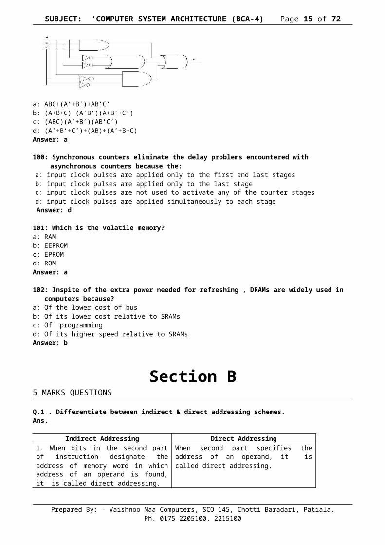
99: the following circuit represents the Boolean expression:
a: ABC+(A’+B’)+AB’C’b: (A+B+C) (A’B’)(A+B’+C’)c: (ABC)(A’+B’)(AB’C’)d: (A’+B’+C’)+(AB)+(A’+B+C) Answer: a
100: Synchronous counters eliminate the delay problems encountered with asynchronous counters because the:
a: input clock pulses are applied only to the first and last stagesb: input clock pulses are applied only to the last stagec: input clock pulses are not used to activate any of the counter stagesd: input clock pulses are applied simultaneously to each stage
Answer: d
101: Which is the volatile memory?a: RAMb: EEPROMc: EPROMd: ROMAnswer: a
Prepared By: - Vaishnoo Maa Computers, SCO 145, Chotti Baradari, Patiala.Ph. 0175-2205100, 2215100

SUBJECT: ‘COMPUTER SYSTEM ARCHITECTURE (BCA-4) Page 13 of 57
102: Inspite of the extra power needed for refreshing , DRAMs are widely used in computers because?a: Of the lower cost of busb: Of its lower cost relative to SRAMsc: Of programmingd: Of its higher speed relative to SRAMsAnswer: b
Section B5 MARKS QUESTIONS
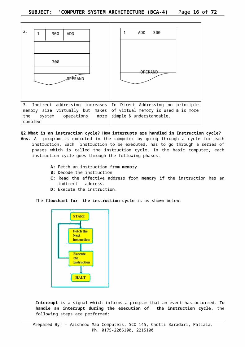
Q.1 . Differentiate between indirect & direct addressing schemes.Ans.
Indirect Addressing Direct Addressing1. When bits in the second part of instruction designate the address of memory word in which address of an operand is found, it is called direct addressing.
When second part specifies the address of an operand, it is called direct addressing.
2.
3. Indirect addressing increases memory size virtually but makes the system operations more complex
In Direct Addressing no principle of virtual memory is used & is more simple & understandable.
Q2.What is an instruction cycle? How interrupts are handled in Instruction cycle?Ans. A program is executed in the computer by going through a cycle for each instruction. Each instruction to
be executed, has to go through a series of phases which is called the instruction cycle. In the basic computer, each instruction cycle goes through the following phases:
A: Fetch an instruction from memoryB: Decode the instructionC: Read the effective address from memory if the instruction has an indirect address.D: Execute the instruction.
The flowchart for the instruction-cycle is as shown below:
Prepared By: - Vaishnoo Maa Computers, SCO 145, Chotti Baradari, Patiala.Ph. 0175-2205100, 2215100
1 300 ADD
300
OPERAND
1 ADD 300
OPERAND

SUBJECT: ‘COMPUTER SYSTEM ARCHITECTURE (BCA-4) Page 14 of 57
Interrupt is a signal which informs a program that an event has occurred. To handle an interrupt during the execution of the instruction cycle, the following steps are performed:
A: Stop the execution of the current instructionB: Save the result of the last executed instruction in a temporary registerC: Set the Program Counter(PC) with the starting address of ISR(Interrupt Service Routine)D: Execute the ISR.
E: Reset the program counter with the address of the next instruction of the executing program.
Q3.Draw and explain the circuit of half adder.Ans. The half adder is a combinational circuit that adds two bits and gives the required result. The input variables of a half-adder are called the augends and addend bits. The output variables of the half adder are known as sum and carry. It is necessary to specify two output variables because the result may consist of two bits. We assign symbols X and Y to the two input variables, and S (for sum) and C (for carry) to the two output variables. The truth table for the half-adder is shown. The C output is 0 unless both inputs are 1. The S output represents the least significant bit of the sum.
The Boolean functions for the two outputs can be obtained directly from the truth table:S (Sum) = x’y+ xy’ = x yC (Carry) = xy
The logic diagram is as shown. It consists of an Exclusive–OR Gate and AND Gate.
A half-adder cannot add 3 bits. For that another combinational circuit is used, called full adder. The half-adder is called so, as two half adders can be employed to implement a full-adder.
Q4.Explain the Design of Full Adder Circuit.
Prepared By: - Vaishnoo Maa Computers, SCO 145, Chotti Baradari, Patiala.Ph. 0175-2205100, 2215100
INPUT OUTPUTX Y S C0 0 0 00 1 1 01 0 1 01 1 0 1
X OR
AND
S
C
X
Y
(a) Truth table(b) Logic diagram
Truth-Table and Circuit of Half adder
SUBJECT: ‘COMPUTER SYSTEM ARCHITECTURE (BCA-4) Page 15 of 57
Ans. A full-adder is a combinational circuit that forms the arithmetic sum of three input bits. It consists of three inputs and two outputs. Two of the input variables, denoted by X and Y, represent the two significant bits to be added. The third input, Z, represents the carry form the previous lower significant position. The two outputs are designated by the symbols S (for sum) and C (for carry). The binary variable S gives the value of the least significant bit of the sum. The binary variable C gives the output carry. The truth table of the full-adder is shown in table. The eight rows under the input variables designate all possible combinations that the binary variables may have. The values of the output variables are determined from the arithmetic sum of the input bits. When all input bits are 0, the output is 0. The S output is equal to 1 when only one input is equal to 1 or when all three inputs are equal to 1. The C output has carry of 1 if two or three inputs are equal to 1.
X Y Z C S 0 0 0 0 0 0 0 1 0 1 0 1 0 0 1 0 1 1 1 0 1 0 0 0 1 1 0 1 1 0 1 1 0 1 0 1 1 1 1 1
The Boolean functions for the outputs C and S are as follows: C = xy + (x’y + xy’)*z C = xy + (x y)*z
S = x y z
Q.5.Explain the fetch and decode phase of the instruction-cycle.Ans. Initially the program counter(PC) is loaded with the first instruction in the program. The sequence counter (SC) is cleared to 0,providinga decoded timing signal T0. After each clock pulse, SC is incremented by one, so that the timing signals go through a sequence T0, T1,T2, and so on. the micro-operations for the fetch and decode phase can be specified by the following register transfer statements:
T0: AR ←PCT1: IR ←M[AR], PC ←PC+1T2: D0,……,D7 ←Decode IR(12-14),AR ←IR(0-11),I←IR(15)
Prepared By: - Vaishnoo Maa Computers, SCO 145, Chotti Baradari, Patiala.Ph. 0175-2205100, 2215100
Logic Diagram and Block Diagram of Full-adder circuit
X
Y
Z
S
C
X
Y
Z
(b) Block diagram
FULLADDER
S
C
Truth Table For Full-Adder Circuit
Inputs Outputs
XOR
AND
XOR
AND
OR
(a) Logic diagram
SUBJECT: ‘COMPUTER SYSTEM ARCHITECTURE (BCA-4) Page 16 of 57
Since only AR is connected to the address inputs of memory, it is necessary to transfer the address from PC to AR during the clock signal associated with timing signal T0. The instruction read from the memory is then placed in the instruction register, IR with the clock transition associated with timing signal T1. At the same time PC is incremented by one to prepare it for the address of the next instruction in the program. At time T 2 , the operation code in IR is decoded,
Q.6.Explain with example the subtraction of two numbers using 2’s Complement method.Ans. Negative numbers are stored as 2’s complement in most computers. The 2’s complement of a number is
obtained by computing 1’s completing and then adding 1 to it. The 1’s complement of a binary number is obtained by changing each 0 to 1 and each 1 to 0.
Steps for subtracting two numbers using 2’s complement method:1. Compute 1’s complement of minuend (i.e. the number that is to be subtracted).2. Compute its 2’s complement by adding 1 to its 1’s complement.3. Add this value with the subtrahend (i.e. the number from which the minuend is to be subtracted).4. Ignore if there is any carry. And if a carry does not occur, take 2’s complement of the number
obtained and place a negative sign in front of the number.
Example: Subtract 0010 from 0110.1. 1’s complement of minuend i.e. of 0010 is 1101. Adding 1 to it, we get 2’s complement of it. 2’s
complement = 1101 + 0001 = 1110.
2. Adding 0110 to 1110, we get 0110 1110
1 01003. Here we have a carry. The carry is neglected in the 2’s complement method. Hence the result is
0110 or in decimal, 4 . We can check the result through decimal representation,0110 is 6 in decimal and 0010 is 2 in decimal. Therefore, 6-2=4, which is the result we got in binary representation as well.
Q7. Convert the following infix expressions into postfix expressions.1) A * B + A * (B * D + C * E)2) A + B * C * D + E * (F+G)3) A * [B + C * (D + E)]
Ans. The above-mentioned expressions are in the infix form. In an infix form, the operator is placed in-between the operands. But when this is to be evaluated by the computer, execution time is wasted as the processor has to move back and forth. This problem is solved, as suggested by Polish mathematician, Jan Lukasiewicz, when the operator is placed either before the operands (referred to as prefix notation) or when the operator is placed after the operands(referred to as postfix notation). To evaluate a postfix notation, the computer uses a stack.Converting the above mentioned infix expressions into postfix form: 1: A * B + A * (B * D + C * E) A* B + A * ( BD* + CE*) A * B + A * BD*CE*+ AB* + ABD*CE*+* AB*ABD*CE*+*+ (postfix form) 2: A + B * C * D + E *(F+G) A + B * C * D + E * FG+ A + BC * * D + E * FG+ A + BC*D* + E * FG+ A + BC*D* + EFG+* ABC*D*+ + EFG+* ABC*D*+EFG+*+ (postfix form)
3: A*(B+C*(D+E)) A*(B+C* DE+) A* (B+ CDE+*) A* BCDE+*+ ABCDE+*+* (postfix form)
Prepared By: - Vaishnoo Maa Computers, SCO 145, Chotti Baradari, Patiala.Ph. 0175-2205100, 2215100

SUBJECT: ‘COMPUTER SYSTEM ARCHITECTURE (BCA-4) Page 17 of 57
Q8.What is a real number or floating-point number? How floating-point numbers are represented in computers?
Ans. A number that has both an integer part as well as fractional part is called real number or floating-point number. For example, 0.756, 1.23, 9.2245 etc. are all floating-point decimal numbers. Similarly, binary real numbers are 1.101, 110.111, 00111.111 etc. The part, which is to the left of the dot, is the integer part and the part, which is to the right of the dot, is called the fractional part. There are two ways of representing floating point numbers in computers. These are:
1) Fixed Point Representation2) Floating Point RepresentationFixed Point Representation: In a fixed point representation of numbers, the binary or decimal point is assumed to be at the extreme right or left of the number. If the binary or decimal point is at the extreme right, the number is an integer. For e.g. 1198 and if the binary or decimal point is at extreme left, the number is a fraction like .9876. This is not a popular method of representation these days because in this method the programmer has to keep track of the location of the decimal or binary point, which is a tedious job.Floating Point Representation: In floating point representation of numbers, the real numbers are stored in computers in the scientific representation form. Thus, in the computer, floating point numbers are represented by two parts:a) Mantissa partb) Exponent partThe mantissa part consists of the signed number and the exponent part indicates the position of the decimal in the number.For example, the decimal number 4598.01 (0.459801 * 104 ) in the floating point representation will be as follows:
Sign Mantissa Sign Exponent 0 .459801 0 04
The zero in the sign bit indicates positive number. The decimal point shown in the mantissa part is not represented in physical form in computers.
Q.9. How is JK flip-flop a refinement over RS flip-flop. Explain.Ans. A JK flip-flop is a refinement over RS flip=flop as the indeterminate state of the RS flip-flop is defined in this flip-flop. Inputs J and K behave like inputs S and R to set and clear the flip-flop. When inputs are applied to both J and K simultaneously, the flip-flop switches to the complement state. A clocked JK flip-flop is as shown below:
JK flip-flop Truth-Table
Output Q is ANDed with K and CP inputs so that the flip-flop is cleared during a clock-pulse only if Q was previously 1. Similarly, output Q’ is ANDed with J and CP inputs so that the flip-flop is set with a clock-pulse only if Q’ was previously 1.
The JK flip-flop behaves just like an RS flip-flop except when both J and K are equal to 1. When both J and K are equal to 1, the clock-pulse is transmitted through one AND gate only, the one whose input is connected to the flip-flop output which is permanently equal to 1.Thus if Q =1, the output of the upper AND gate becomes 1 upon the application of a clock-pulse, and the flip-flop is cleared. If Q’=1,the output of the lower AND gate becomes a 1 and the flip-flop is set. In either case, the output state of the flip-flop is complemented.
Q.10.What are addressing modes? Explain its types.Ans. The various types of addressing modes are as follows: -
Prepared By: - Vaishnoo Maa Computers, SCO 145, Chotti Baradari, Patiala.Ph. 0175-2205100, 2215100
Q J K Q(t+1)0 0 0 00 0 1 00 1 0 10 1 1 11 0 0 11 0 1 01 1 0 11 1 1 0

SUBJECT: ‘COMPUTER SYSTEM ARCHITECTURE (BCA-4) Page 18 of 57
1. Implied mode: - In this mode the operands are specified implicitly in the definition of instructions. For example Instruction for “complement” is an implied mode instruction because the operand in the accumulator register is implied in the definition of instruction.
2. Immediate Mode: -In this mode the operand is specified in the instruction itself. In other words, and immediate-mode instruction has an operand field rather that an address field. The operand field contains the actual operand to be used in conjunction with the operation specified in the instruction.
3. Register mode: In this mode the operands are in registers that reside with in the CPU. The particular register is selected from a register field. In the instruction, A k-bit field can specify any one of 2k registers.
4. Register indirect mode: - In this mode the instructions specifies a register in the CPU whose contents give the address of operand in memory. In other words selected register contains address of operand rather than operand itself.
5. Direct address mode: -In this mode the effective address is equal to the address part of instruction. The operand resides in memory and its address is given directly by address field of the instructions. In a branch type instruction address field specifies the actual branch address.
6. Indirect address mode: -In this mode the address field of the instruction gives the address where the effective address is stored in memory. Control fetches the instruction from memory and uses its address part to access memory again to read the effective address.
7. Relative address mode: -In this mode the content of program counter is added to the address part of the instruction in order to obtain the effective address. The address part of instruction is usually a signed number, which can be either positive or negative.
8. Indexed addressing mode: -In this mode the content of then index register is added to the address part of the instruction to obtain effective address. The index register is a special CPU register that contains an index value. The address field of an instruction defines the beginning address of data array in memory.
9. Base register addressing mode: In this mode the contents of base register are added to address part of the instruction to obtain the effective address. This is similar to indexed addressing mode except that register is base register instead of index register.
Q.11. List various types of registers. Briefly describe their functionsAns. A processor often contains several kinds of registers that can be classified according to their content or
instructions that operate on them:
1. Data Registers – Its size is 16 bits and it is used to hold the memory operand. It is referred to as DR.
2. Address Register- This register is referred as AR and is of 12-bit size as this is the size of a memory address. Address registers hold addresses and are used by instructions that indirectly access memory.
3. Accumulator- In some older and low end CPUs, a special data register, known as the accumulator, referred as AC, is used implicitly. AC is used to manipulate data. Like data register, it is also of 16 bits.
4. Program Counter- Referred as PC, it is of 12-bit size. It holds the address of the next instruction that is to be read from memory after the current instruction is executed.
5. Instruction Register- Referred to as IR, it is of 16-bit size and is used to hold the code of the instruction.
6. Input Register-Referred to as INPR, it is of 8-bit size. It holds the input characters.
7. Output Register-This register is referred to as OUTR and is of 8-bit size. It holds the output characters.
8. Temporary Register- This is used to hold temporary data generated during the execution of the instruction. It is referred to as TR and is of 16-bit size.
The number of registers in a computer and their storing capacity determine the power of the computer. The register-size is also known as word-size which represents the number of bits, a register can manipulate at a time.
Prepared By: - Vaishnoo Maa Computers, SCO 145, Chotti Baradari, Patiala.Ph. 0175-2205100, 2215100

SUBJECT: ‘COMPUTER SYSTEM ARCHITECTURE (BCA-4) Page 19 of 57
Q.12- What is BCD? What are the rules of BCD addition? Ans. BCD is short for Binary Coded Decimal. In BCD system, each digit is represented by a nibble, which is binary code of four digits. To represent a number in BCD system, each digit is replaced by an appropriate four-bit code.
The following table shows BCD codes for decimal numbers:
Decimal BCD code0 00001 00012 00103 00114 01005 01016 01107 01118 10009 1001
For eg. The decimal number 980 is represented in BCD as: 1001 1000 0000
The rules for BCD addition are: Add two numbers using binary addition. If four-bit sum is equal or less than 1001,then it is a valid BCD
number.
If a 4-bit sum is greater than 1001 or a carry is generated from the group of 4 bits, the result is invalid. In such a case 0110 should be added to the 4-bit sum. If a carry is generated when adding 0110, the carry is added to the next 4-bit group.
For example, to add 2 and 6,using:
001001101000
As this sum is less than 1001, hence the answer would remain the same, i.e. 1000
Now, in the other example, we add 6 and 8:01101000
1110 As 1110 is greater than 1001, we add: 0110 to it :
11100110
10100 As still a carry is generated, we add this carry to the next 4-bit group: The answer now becomes: 00010100
Q.13.What are the various advantages and disadvantages of Assembly Language programs? What are the various rules of the assembly language?
Ans. Advantages of Assembly Language Programs:1. Assembly language programs use less of computer’s main memory as compared to High Level
Language Programs.2. An assembly language program needs less processing power of a CPU and thus runs faster than
high level language program.3. Compared to machine language, assembly language is a better option as it involves the usage of
mnemonics which are somewhat understandable to the programmer.Disadvantages of Assembly Language Programs1. Programming is difficult and debugging is time consuming.2. In order to write an assembly language program, a programmer must have detailed knowledge of
the structure of the computer he is using, including the knowledge of registers, instruction set of the computer, connection of ports to the peripherals, etc.
Prepared By: - Vaishnoo Maa Computers, SCO 145, Chotti Baradari, Patiala.Ph. 0175-2205100, 2215100

SUBJECT: ‘COMPUTER SYSTEM ARCHITECTURE (BCA-4) Page 20 of 57
3. The program written for one computer cannot be used for another computer of a different make.4. The assembly language program has to converted into machine language using assembler and can
not be executed directly like a machine-level program.
. Like every programming language assembly language also has some syntax and semantics that the programmer must follow. Following are the rules of the assembly language:
The basic unit of an assembly language program is a line of code. Each line of code must be divided into four fields as follows:
Label, Instruction and Comment The label field must specify the location of the instruction in the memory in symbolic form (symbolic
address). The label field may be empty also. The label in the label field is terminated by a comma (,) so that the assembler recognizes it as a
label. It can contain one to three alphanumeric characters. The first character must be a letter. The next two characters may be letter or numerals.
A symbolic address in the instruction field specifies the memory location of an operand. The instruction field must specify a mnemonic instruction or a pseudo-instruction. The comment field can be left empty or it may include a comment. Comment field is for the
programmer or any one else who may read the program and should be able to understand it.
Eg. ADD B /Add operand from memory location B.
Q.14.Discuss the various types of instruction formats..Ans. An instruction is a combination of bits used to perform memory-related operations. The basic computer
has three instruction code formats. Each format has 16 bits. The following are the instruction- format categories:
1. Memory Reference Instruction: It is used to perform memory-related operations. A memory reference instruction format uses 12 bits to specify and address part of the instruction, i.e. bits 0 to 11. Opcodes occupies the bits from 12 to 14 and 1 bit to specify the mode. The values of opcode field for memory reference instructions are from 000 to 110.
1 Opcode Address
15 14 12 11 0(Opcode = 000 through 110)
Memory Reference instruction
2. Register Reference Instruction: It is used to perform operations related to processor register. The instruction code format is divided into three parts: register operation, opcode and instruction-type. The register operation is specified by the bits: 0 to 11. Bits 12 to 14 specify the opcode and bit 15 is used to specify whether the instruction is of register type or not. A register reference instruction is recognized by the value of 111 in the opcode field and 0 as its 15th bit.
15 14 12 11 0 0 111 Register Operation
(Opcode = 111, I = 0) Register Reference instruction
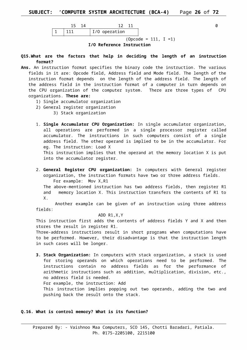
3. Input-Output(I/O) reference Instruction: Used to perform operations related to input and output of data. The instruction code format of this instruction is divided into three parts: I/O operation, Opcode and instruction-type. The I/O operation parts occupies bits 0 to 11. 12 to 14 are occupied by Opcode and 15th bit is used to specify that the instruction is an I/O type of instruction. An I/O reference instruction is recognized by the value of 111 in the opcode field and 1 as its 15 th bit.
15 14 12 11 01 111 I/O operation
(Opcode = 111, I =1) I/O Reference Instruction
Q15.What are the factors that help in deciding the length of an instruction format?Ans. An instruction format specifies the binary code the instruction. The various fields in it are: Opcode field,
Address field and Mode field. The length of the instruction format depends on the length of the address
Prepared By: - Vaishnoo Maa Computers, SCO 145, Chotti Baradari, Patiala.Ph. 0175-2205100, 2215100

SUBJECT: ‘COMPUTER SYSTEM ARCHITECTURE (BCA-4) Page 21 of 57
field. The length of the address field in the instruction format of a computer in turn depends on the CPU organization of the computer system. There are three types of CPU organizations. These are:
1) Single accumulator organization2) General register organization
3) Stack organization
1. Single Accumulator CPU Organization: In single accumulator organization, all operations are performed in a single processor register called accumulator. The instructions in such computers consist of a single address field. The other operand is implied to be in the accumulator. For eg. The instruction: Load X This instruction implies that the operand at the memory location X is put into the accumulator register.
2. General Register CPU organization: In computers with General register organization, the instruction formats have two or three address fields.
For example: Mov X,R1 The above-mentioned instruction has two address fields, then register R1 and memory location X. This instruction transfers the contents of R1 to X.
Another example can be given of an instruction using three address fields: ADD R1,X,Y
This instruction first adds the contents of address fields Y and X and then stores the result in register R1.Three-address instructions result in short programs when computations have to be performed. However, their disadvantage is that the instruction length in such cases will be longer.
3. Stack Organization: In computers with stack organization, a stack is used for storing operands on which operations need to be performed. The instructions contain no address fields as for the performance of arithmetic instructions such as addition, multiplication, division, etc., no address field is needed. For example, the instruction: AddThis instruction implies popping out two operands, adding the two and pushing back the result onto the stack.
Q.16. What is control memory? What is its function?Ans. In a micro-programmed control unit, the binary control variables are stored in control memory. Each word in control memory contains a micro-instruction. The micro-instruction specifies one or more micro-operations for the system. A sequence of micro-instructions constitutes a micro-program. Since alterations of the micro-program are not needed once the control unit is in operation, the control memory can be a read-only memory (ROM).
A computer that employs a micro-programmed control unit has two separate memories: main memory and control memory. The main memory is available to the user for storing the programs. The contents of main memory may alter when the data are manipulated and every time the program is changed. In contrast, the control memory holds a fixed micro-program that cannot be altered by the occasional use.
The control memory is thus assumed to be a ROM, within which all control information is permanently stored. The control memory address register specifies the address of the micro-instruction and the control data register holds the micro-instruction read from memory. The data register is sometimes called pipeline register. While the micro-operations are being executed, the next address is computed in the next address generator circuit and then transferred into the control address register to read the next micro-instruction. The next address generator is sometimes called a micro-program sequencer as it determines the address sequence that is read from control memory.
Q.17 What are the various registers used in the DMA controller? What is the use of each and every register?Ans. The transfer of data between a fast storage device such as magnetic disk is often limited by the speed of
the CPU. Removing the CPU from the path and letting the peripheral device manage the memory buses directly would improve the transfer. This transfer technique is called direct memory access. During DMA transfer, the CPU is idle and has no control of the memory buses. A DMA controller takes control over the buses to manage the transfer directly between the I/O device and memory.
In DMA controller three registers are mainly used:
Prepared By: - Vaishnoo Maa Computers, SCO 145, Chotti Baradari, Patiala.Ph. 0175-2205100, 2215100
SUBJECT: ‘COMPUTER SYSTEM ARCHITECTURE (BCA-4) Page 22 of 57
1) Address Register2) Word Count Register3) Control Register
1) Address Register: Address register contains the address of memory where the data from the input device needs to be stored or from where the data for output device needs to be fetched. CPU gives this address to the data bus. The address is transferred to the address register from the data bus through internal bus. Address in this register is incremented after transferring each word to or from memory. This is done so that the address register now points to the address of next word in the sequence.
2) Word Count Register: Word Count Register stores the number of words that need to be read from or written into memory. It is decremented after each word transfer. When the value in this register becomes zero, it is assumed that data transfer has completed.
3) Control Register: The control register specifies the mode of the data transfer, i.e. whether it is a read operation or it is a write operation. CPU supplies the contents of these registers through the data bus.
Q.18.Explain about input output processor (IOP) in detail. Ans. Input/Output Processor: Instead of having each interface communicate with the CPU, a computer may
incorporate one or more external processors and assign them the task of communicating directly with all I/O devices. An input-output processor (IOP) may be classified as a processor with direct memory access capability that communicates with I/O devices. In this configuration, the computer system can be divided into a memory unit, and a number of processors comprised of the CPU and one or more IOPs. Each IOP takes care of input and output tasks. An IOP is also known as a channel.
The IOP is similar to a CPU except that it is designed to handle the details of I/O processing. Unlike the DMA controller that must be set up entirely by the CPU, the IOP can fetch and execute its own instructions. IOP instructions are
BLOCK DIAGRAM OF A COMPUTER WITH I/O PROCESSOR
specifically designed to facilitate I/O transfers. In addition, the IOP can perform other processing tasks, such as arithmetic, logic, branching, and code translation. The block diagram of a computer with two processors is shown in the figure above. The memory unit occupies a central position and can communicate with each processor by means of direct memory access. The IOP provides a path for transfer of data between various peripheral devices and the memory unit. The CPU is usually assigned the task of initiating the I/O program. After that the IOP operates independent of the CPU and continues to transfer data from external devices and memory.
Q.19.Explain Direct Memory Access (DMA) with the help of diagram.Ans. The transfer of data between a fast storage device such as magnetic disk is often limited by the speed of
the CPU. Removing the CPU from the path and letting the peripheral device manage the memory buses directly would improve the transfer. This transfer technique is called direct memory access. During DMA transfer, the CPU is idle and has no control of the memory buses. A DMA controller takes control over the buses to manage the transfer directly between the I/O device and memory.
Prepared By: - Vaishnoo Maa Computers, SCO 145, Chotti Baradari, Patiala.Ph. 0175-2205100, 2215100
Memory Unit
Central Processing
Unit
Input-OutputProcessor
(IOP)
PD
PD
PD
Peripheral Devices

SUBJECT: ‘COMPUTER SYSTEM ARCHITECTURE (BCA-4) Page 23 of 57
When the DMA takes control of the bus system, it communicates directly with the memory. The transfer can be made in one of the two possible ways:1. Burst Transfer: In DMA burst transfer; a block sequence consisting of a number of memory words
is transferred in a continuous burst while the DMA controller is master of the memory buses. This mode of transfer is needed for fast devices such as magnetic disks where data transmission cannot be stopped or slowed down until an entire block is transferred.
2. Cycle Stealing: This technique allows the DMA controller to transfer one data word at a time, after which it must return control of the buses to the CPU. The CPU merely delays its operation for one memory cycle to allow the direct memory I/O transfer to “steal” one memory cycle.
The DMA is first initialized by the CPU. After that, the DMA starts and continues to transfer data between memory and peripheral unit until an entire block is transferred. The initialization process is essentially a program consisting of I/O instructions that include the address for selecting particular DMA registers. The CPU initializes the DMA by sending the following information through the data bus:1. The starting address of the memory block where data are available (for read) or where data are to
be stored.2. The word count, which is the number of words in the memory block.3. Control to specify the mode of transfer such as read or write.4. A control to start the DMA transfer.
Q.20.What is a peripheral device? What are the commonly used peripheral devices. Ans. Peripheral Device: Input or output devices and secondary storage devices attached to the computer are
known as peripheral devices. The most common peripheral devices are:
1. Monitor and Keyboard: A keyboard as an input device and monitor is an output device. In normal usage, the keyboard is used to type text and numbers into a word processor, text editor or other programs. In a modern computer, the interpretation of key presses is generally left to the software. A computer keyboard distinguishes each physical key from every other and reports all key presses to the controlling software. Keyboards are the only There are different types of video monitors, but the most popular used is cathode ray tube (CRT). The CRT contains an electronic gun that sends an electron beam to a phosphorescent screen in front of the tube. The beam can be deflected horizontally and vertically. Horizontal and vertical signals deflect the beam and make it sweep across the tube, causing the visual pattern to appear on the screen. A characteristic feature of display devices is a cursor that marks the position in the screen where the next character will be inserted. The display terminal can operate in a single-character mode where
Prepared By: - Vaishnoo Maa Computers, SCO 145, Chotti Baradari, Patiala.Ph. 0175-2205100, 2215100
DS
DMA acknowledge
Data Bus
Address Bus
DS
RS
RD
WRBR
BG
INT
Address Bus buffers
Address Register
Word Count Register
Control Register
Data Bus Buffers
DMA requestTo I/O device
Block Diagram of DMA controller
ControlLogic

SUBJECT: ‘COMPUTER SYSTEM ARCHITECTURE (BCA-4) Page 24 of 57
all characters entered on the screen through the keyboard are transmitted to the computer simultaneously. In the block mode, the edited text is first stored in a local memory inside the terminal. The text is transferred to the computer as a block of data.
2. Printers: Printers provide a permanent record on paper of computer output data or text. There are three basic types of character printers: Daisywheel, dot matrix and laser printers. The daisywheel printer contains a wheel with the characters placed along the circumference. To print a character, the wheel rotates to the proper position and the energized magnet presses the character against the ribbon. The dot matrix printer contains a set of dots along the printing mechanism. For example, a 5*7 dot matrix printer that prints 80 characters per line has seven horizontal lines, each consisting of 5*80=400 dots. Each dot may be printed or not, depending on the specific characters that are printed on the line. The laser printer uses a rotating photographic drum that is used to imprint the character images. The pattern is then transferred onto paper in the same manner as a copying machine.
3. Magnetic Tapes and Magnetic disks: These are used to store the data in bulk amount. Both magnetic tapes and disks perform the same task with the only difference that a magnetic disk has high speed of data access.
Other peripherals that may be connected to the computer according to the need include light pen, joystick, scanner, optical reader, etc.
Q.21. Explain priority interrupt. Ans. A priority interrupt is a system that establishes a priority over the various sources to determine the condition which is to be serviced first, when two or more requests arrive simultaneously. The system may also determine which conditions are permitted to interrupt the computer while another interrupt is being serviced. Higher priority interrupt levels are assigned to requests which, if delay or interrupted, could have serious consequences. When two devices interrupt the computer at the same time, the computer services the device, with the higher priority first. Establishing the priority of simultaneous interrupts can be done by software or hardware.
A polling procedure is used to identify the highest priority source by software means. In this method there is one common branch addresses for all interrupts the Program that takes care of interrupts polls the interrupt sources in sequence. The order in which they are tested determines the priority of each interrupt. The initial service routine for all interrupts consists of a program that tests the interrupt sources in sequence and branches to one of many possible services routines. The particular service routine reached belongs to the highest-priority device among all devices interrupted the computer. The drawback of the software method is that, the time required to poll them can exceed the time available to service the I/O device, if there are many interrupts.
A hardware priority-interrupt unit functions as an overall manager in an interrupt system environment. Each interrupt source has its own interrupt vector to access its own service routine directly, to speed up the operation. The hardware priority function can be established by either a serial or a parallel connection of interrupt lines. The serial connection is also known as the daisy-chaining method.Daisy-chaining Priority : The daisy-chaining method of establishing priority consists of a serial connection of all devices that request an interrupt. The device with the highest priority is placed in the first position, followed by lower-priority devices up to the device with the lowest priority, which is placed last in the chain. The daisy chain arrangement gives the highest priority to the device that receives the interrupt acknowledge signal from the CPU. The farther the device is from the first position; the lower is its priority.Parallel Priority Interrupt: The parallel priority interrupt method uses a register whose bits are set separately by the interrupt signal from each device. Priority is established according to the position of the bits in the register. The circuit may include a mask register whose purpose is to control the status of each interrupt request in addition to the interrupt register. The mask register can be programmed to disable lower-priority interrupts while a higher priority device is being serviced. It also provides a facility that allows a high priority device to interrupt the CPU while a lower-priority device is being serviced.
Q.22.Explain asynchronous serial data transmission in detail.Ans. Asynchronous Serial data Transmission: The transfer of data between two units is parallel and serial.
In serial data transmission, each bit in the message is sent in sequence one at a time. A serial asynchronous data transmission technique used in many interactive terminals employs special bits that are inserted at both ends of the character code. With this technique, each character consists of three parts: starts bit, the character bits, and stop bits. The transmitter rests at 1-state when no characters are transmitted. The first bit, called the start bit, is always a 0 and is used to indicate the beginning of a
Prepared By: - Vaishnoo Maa Computers, SCO 145, Chotti Baradari, Patiala.Ph. 0175-2205100, 2215100

SUBJECT: ‘COMPUTER SYSTEM ARCHITECTURE (BCA-4) Page 25 of 57
character. The last bit called the stop bit is always a 1. An example of this format is shown in the following figure:
1 1 0 0 0 1 0 1
start character bits Stop bits bit
A transmitted character can be detected by the receiver from the knowledge of the following transmission rules:
1. When a character is not being sent, the line is kept in the 1-state.
2. The initiation of a character transmission is detected from the start bit, which is always 0.
3. The character bits always follow the start bit.
4. After the last bit of the character is transmitted, a stop bit is detected when the line returns to the 1-state for at least one bit time.
Q23. Explain asynchronous data transfer using handshaking.Ans. Asynchronous data transfer using handshaking: Asynchronous data transfer between two
independent units requires that control signals be transmitted between the communicating units to indicate the time at which data is being transmitted. One way of achieving this is by means of strobe pulse supplied by one of the units to indicate to the other unit when the transfer has to occur. Another method commonly used is to accompany each data item being transferred with a control signal that indicates the presence of data in a bus. The unit receiving the data item responds with another control signal to acknowledge receipt of the data. This type of agreement between two independent units is referred to as handshaking.
The block-diagram of source-initiated transfer using handshaking, is as shown below:
The source initiates the transfer by placing the data on the bus and enabling its data-valid signal. The data-accepted signal is activated by the destination unit after is accepts data from the bus. The source-unit then disables its data-valid signal which invalidates the data on the bus. The destination unit then disables its data accepted signal and the system goes into the initial state. Only after the data accepted signal is disabled by the destination, the source sends new data.
In the destination-initiated data transfer, the source unit does not place data on the data bus until it receives ‘ready for data ‘ signal from the destination unit. From there-on, the handshaking procedure follows the same pattern as in the source-initiated case. The block-diagram for destination-initiated data transfer using handshaking, is as shown below:
Prepared By: - Vaishnoo Maa Computers, SCO 145, Chotti Baradari, Patiala.Ph. 0175-2205100, 2215100
Source Unit
Destination Unit
Data bus
Data valid
Data Accepted
Source Unit
Destination Unit
Data bus
Data valid
Ready for data
SUBJECT: ‘COMPUTER SYSTEM ARCHITECTURE (BCA-4) Page 26 of 57
Q.24.a:) What do you mean by micro-programmed control unit? How micro-programmed control unit is used in addressing sequence?
b:) Differentiate between Microinstruction & Macroinstruction.
Ans. a:)When microprogramming is used to design control unit of a digital computer, it is called micro-programmed control unit i.e.. Microprogramming provides efficient & systematic method for controlling the micro-operation sequences in a digital computer. In this technique we use string of 1’s & 0’s called a control word, which is programmed to perform various operations on the components of the system.
Microprogrammed control unit is used in addressing sequence as follows:Here, Microinstructions are stored in control memory in groups, with each group specifying a Routine. Steps that must be performed during the execution of a single computer instruction are:
1. Increment contents of control address register.2. Unconditional branch or conditional branch is allocated depending on status bit conditions.3. A mapping process followed from bits of instructions to an address for control memory.4. Lastly, facility is used for subroutine call & return.
b) Differences between micro-instruction and macro-instruction are as listed below:
Microinstruction MacroinstructionMicro instruction specifies one or more micro-operation for the system
Macroinstruction specifies one or more macro operation for the system
Sequence of micro instructions constitutes a micro program
Sequence of Macro instructions is called macro program
Alterations in micro instructions cannot be done once control unit is in operation
Alterations are possible at any time in macroinstructions
The contents of a word in ROM at a given address specifies a microinstruction
The contents of word in RAM, at an address specifies a macro instruction
Each word in control memory contains within it a microinstruction
Each string of words in control memory contains with in it a macroinstruction
Q.25.What is the need of an I/O interface?Ans. An Input/Output interface provides a method for transferring information between internal storage and
external I/O devices. Peripherals connected to a computer need special communication links for interfacing them with the CPU. The purpose of the communication link is to resolve the differences that exist between the CPU and each peripheral. The major differences between the CPU and peripherals due to which an I/O interface is needed, are:
1. Peripherals are electromagnetic and electromechanical devices and their manner of operation is different from the operation of the CPU and memory which are electronic devices. Hence a conversion of signal values may be needed.
2. The data transfer-rate of peripherals is usually slower than the transfer rate of the CPU and hence a synchronization mechanism is needed.
3. Data codes and formats in peripherals differ from the word-formats in CPU and memory.
4. The operating modes of the peripherals are different from each other and each must be controlled so as not to disturb the operation of other peripherals connected to the CPU.
Prepared By: - Vaishnoo Maa Computers, SCO 145, Chotti Baradari, Patiala.Ph. 0175-2205100, 2215100
SUBJECT: ‘COMPUTER SYSTEM ARCHITECTURE (BCA-4) Page 27 of 57
Inorder to resolve these differences, computer systems include special hardware components between the CPU and the peripherals to supervise and synchronize all input and output transfers. These components are called interface units because they interface between the processor bus and the peripheral device.
Q.26. What are the different types of channels? What are the various word-formats used by these channels.
Ans. Channels are used to handle the I/O operation of computer system. The channel is also referred to as an I/O processor. The number of channels connected to the computer depends on the basis of the applications running on the system. Each channel handles the processing of one or more I/O devices connected to it. The various types of channels are:
1. Multiplexed channels- These are connected to peripherals of slow and medium access speed and can process various I/O devices simultaneously.
2. Selector channels- These are connected to peripherals of high access speed and can process one peripheral at a time.
3. Block Multiplexer channels- These are connected to various peripherals of high access speed and can process various peripherals simultaneously.
There are three types of word-formats of a channel which are as follows:
I/O Instruction word format – This word format is divided into three parts: operation code, channel address and device address. Operation code specifies the type of operation to be performed on peripherals. Channel address is used to specify the address of the channel which is used to perform operation on the peripheral. The address of the peripheral is stored in the device address part of the I/O instruction word format.
I/O Instruction Format
Channel Status word format- It is divided into four parts: key, address, status and count. The key is used to provide a protection-mechanism to the information of a user from unauthorized access. The address part is used to specify the address of the last command word used by the channel. Status is used to specify error conditions in the peripheral and channel which terminates the data transfer. If the data is transmitted successfully, the value of the status part becomes 0.Count is used to specify the residual count when the data transfer gets terminated.
Channel Status Word Format
Channel command word format- This is divided into four parts: command code, data address, flags and count. Data address specifies the first address of the memory where the data is stored. Count is used to specify the total number of bytes involved in the transfer. Flag is used to specify the status of the channel. Command code specifies the operation that is to be performed by the channel.
Channel command word format
Q26.What is cache memory? What is locality of reference and hit ratio associated with cache memory?
Prepared By: - Vaishnoo Maa Computers, SCO 145, Chotti Baradari, Patiala.Ph. 0175-2205100, 2215100
Operation Channel DeviceCode Address Address
Key Address Status Count
Command Data Address Flag Count Code

SUBJECT: ‘COMPUTER SYSTEM ARCHITECTURE (BCA-4) Page 28 of 57
Ans. Cache Memory: A special very high-speed memory called a cache is sometimes used to increase the speed of processing by making current programs and data available to the CPU at a rapid rate. The Cache memory is employed in computer systems to compensate for the speed differential between main memory access time and processor logic.
Locality of Reference: The phenomenon in which the references to memory at any given interval of time tends to be confined within a few localized areas of memory is known as the property of locality of reference. A typical computer program follows a straight line with loops and subroutine calls encountered frequently. Whenever this happens, the CPU repeatedly refers to the set of instructions in memory that constitute these. Thus loops and subroutines tend to localize the references to memory for fetching instructions. To a lesser degree, memory references to data also tend to be localized. If the active programs and data are placed in cache memory, this would reduce the program execution time.
Hit Ratio: The performance of Cache Memory is measured in terms of Hit Ratio. If a data item requested by the CPU is found in the cache, it is called a hit. If the requested data item is not found, it is called a miss. Hit Ratio is the ratio of number of hits divided by the total requests or the number of hits divided by the (total number of hits and total number of misses).
Number of hitsHit Ratio =
Number of hits + Number of missesQ.27.What is memory hierarchy? Ans. Memory hierarchy: The memory unit is an essential component in any digital computer since it is needed
for storing programs and data. The memory hierarchy system consists of all storage devices employed in a computer system from the slow but high-capacity auxiliary memory to a relatively faster main memory, to an even smaller and faster cache memory accessible to the high-speed processor logic. Although the main/auxiliary memory distinction is broadly useful, memory organization in a computer forms a hierarchy of levels, arranged from very small, fast, and expensive registers in the CPU to small, fast cache memory; larger DRAM; very large hard disks; and slow and inexpensive nonvolatile backup storage. The various memories that are the part of the memory hierarchy are:Auxiliary Memory: Devices that provide backup storage are called auxiliary memory. The most common auxiliary memory devices used in computer systems are magnetic tapes and disks. They are used for storing system programs, large data files, and other backup information.
Main Memory: The memory unit that communicates directly with the CPU is called Main memory. The main memory occupies a central position in memory hierarchy by being able to communicate directly with the CPU and with auxiliary memory devices through an I/O processor.Cache Memory: A special very high-speed memory called a cache is sometimes used to increase the speed of processing by making current programs and data available to the CPU at a rapid rate. The Cache memory is employed in computer systems to compensate for the speed differential between main memory access time and processor logic.
Q.28.How is Cache Memory initialized?
Prepared By: - Vaishnoo Maa Computers, SCO 145, Chotti Baradari, Patiala.Ph. 0175-2205100, 2215100
Magnetic tapes
Magnetic disks
I/O PROCESSORMain Memory
Cache Memory
CPU
Memory Hierarchy in a computer system

SUBJECT: ‘COMPUTER SYSTEM ARCHITECTURE (BCA-4) Page 29 of 57
Ans. A special very high-speed memory called a cache is sometimes used to increase the speed of processing by making current programs and data available to the CPU at a rapid rate. The Cache memory is employed in computer systems to compensate for the speed differential between main memory access time and processor logic.
One important aspect of cache organization that must be taken into consideration is the problem of initialization. The cache is initialized when power is applied to the computer or when the main memory is loaded with a complete set of programs from auxiliary memory. After initialization, the cache is considered to be empty, but in effect it contains some non-valid data. It is customary to include with each word in cache, a valid bit to indicate whether or not the word contains valid data.
The cache is initialized by clearing all the valid bits to 0. The valid bit of a particular cache word is set to 1, the first time this word is loaded from main memory and stays set unless the cache has to be initialized again. The introduction of the valid bit means that a word in cache is not replaced by another word unless the valid bit is set to 1 and a mismatch of tags occurs. If the valid bit is zero, the new word automatically replaces with the invalid data. In this way, the cache memory is initialized.
Q.29. Explain associative memory. Ans. A memory that is addressed by the content of the data is called an associative memory or content addressable memory(CAM).This type of memory is accessed simultaneously and in parallel on the basis of data content rather than by specific address or location. When a word is written in an associative memory, no address is given. The memory is capable of finding an empty or unused location to store the word. When a word is to be read from an associative memory, the content of the word, or part of the word, is specified. The memory locates all words which match the specified content and marks them for reading.
The block-diagram of associatve memory is as shown below:
The components in the diagram above are as shown below:
Associative memory- It holds m words where each word consists of n bits.
Argument register- It is an n-bit register and stores the word which is to be searched inside the associative memory.
Key register-It is also an n-bit register which hold the key for performing the search inside the associative memory.If all bit positions inside the key register are set to 1 then the entire word specified in the argument register is compared with each word inside the memory else only those bits in the argument register which have 1 in the corresponding position inside the key register are compared.
Match register- It is an m-bit register, where each bit corresponds to a word inside the associative memory. Each bit of the register is set if the word in associative memory matches with the word in the argument register.
Prepared By: - Vaishnoo Maa Computers, SCO 145, Chotti Baradari, Patiala.Ph. 0175-2205100, 2215100
SUBJECT: ‘COMPUTER SYSTEM ARCHITECTURE (BCA-4) Page 30 of 57
Q.5. What is virtual memory?Ans. Virtual Memory is a cost effective solution for applications requiring extra memory. Basically two types of memory are needed in this system. Random Access Memory (RAM) which is faster but costly. Memory like hard disk which is slower but relatively cheaper. Virtual memory is a strategy to utilize the hard drive memory to achieve enhanced performance from the random access memory.
Whenever multiple programs/applications are running on the system, the user generally works on only a portion of a particular application at an instant. Therefore it is a waste of resource to load the entire memory required for a particular application into the limited- size random access main memory. In a virtual memory environment, each page of a process is brought to main memory only when it is needed on demand, else it remains on the hard disk..
Data is stored in any memory in the form of binary digits. The operating system handles memory management in the form of chunks of memory called pages. A page is nothing but a contiguous block of memory. One process might require multiple pages of memory but only a few pages might be active at a time. Virtual memory uses a technique called demand paging to effectively use the available RAM memory. Every page has an address which may be a virtual or logical address. The main memory is divided into equal size chunks called page frames and each page frame has a unique physical address. So whenever a page needs to be accessed, the operating system has to translate the virtual address into a physical address and this is done by a Memory Management Unit (MMU) with the help of mapping in a page table. The virtual address corresponding to a page is mapped to a physical address corresponding to a page frame in main memory. Whenever a page is not in memory the operating system fetches the page from hard disk in response to a page fault exception. The operating system usually makes a prediction based on past history using intelligent algorithms regarding those pages that are least likely to be needed again and places them in the hard disk.
Q.30.What is demand paging?Ans. In computer operating systems, demand paging is a method of virtual memory management. In a system that uses demand paging, the operating system copies a disk page into physical memory only if an attempt is made to access it (i.e., if a page fault occurs). It follows that a process begins execution with none of its pages in physical memory, and many page faults will occur until most of a process's working set of pages is located in physical memory. Demand paging follows that pages should only be brought into memory if the executing process demands them. This is often referred to as lazy evaluation as only those pages demanded by the process are swapped from secondary storage to main memory.
Commonly, to achieve this process a page table implementation is used. The page table maps logical memory to physical memory. The page table uses a bitwise operator to mark if a page is valid or invalid. A valid page is one that currently resides in main memory. An invalid page is one that currently resides in secondary memory. When a process tries to access a page, the following steps are generally followed:
Attempt to access page. If page is valid (in memory) then continue processing instruction as normal. If page is invalid then a page-fault trap occurs. Check if the memory reference is a valid reference to a location on secondary memory. If not, the
process is terminated (illegal memory access). Otherwise, we have to page in the required page. Schedule disk operation to read the desired page into main memory. Restart the instruction that was interrupted by the operating system trap.
Demand paging is explained through he following diagram:
Prepared By: - Vaishnoo Maa Computers, SCO 145, Chotti Baradari, Patiala.Ph. 0175-2205100, 2215100

SUBJECT: ‘COMPUTER SYSTEM ARCHITECTURE (BCA-4) Page 31 of 57
Demand paging, helps in loading only those pages that are demanded by the executing process and as main memory is expensive compared to secondary memory, this technique helps significantly in reducing the cost.
Q.31. Explain the difference between Intel 8080 and 8085 processors.Ans. The Intel 8080 was the second 8-bit microprocessor designed and manufactured by Intel and was released in April 1974. It was an extended and enhanced variant of the earlier 8008 design, although without binary compatibility. The 8080 has sometimes been labeled "the first truly usable microprocessor". The 8080 was implemented demands an extra +12 volt and a −5 volt supply. It used the same basic instruction set as the 8008 but added some handy 16-bit operations to the instruction set. The 8080's large 40-pin DIP packaging permitted it to provide a 16-bit address bus and an 8-bit data bus, allowing easy access to 64 kilobytes of memory. The processor had seven 8-bit registers, (A, B, C, D, E, H, and L) where A was the 8-bit accumulator and the other six could be used as either byte-registers or as three 16-bit register pairs (BC, DE, HL) depending on the particular instruction. It also had a 16-bit stack pointer to memory and a 16-bit program counter. As with many other 8-bit processors, all instructions were encoded in a single byte. Most 8-bit operations could only be performed on the 8-bit accumulator. Although the 8080 was generally an 8-bit processor, it also had limited abilities to perform 16-bit operations. The 8080 supported up to 256 input/output (I/O) ports, accessed via dedicated I/O instructions—taking port addresses as operands. This I/O mapping scheme was regarded as an advantage, as it freed up the processor's limited address space.
The Intel 8085 is an 8-bit microprocessor introduced by Intel in 1977. It was binary-compatible with the more-famous Intel 8080 but required less supporting hardware, thus allowing simpler and less expensive microcomputer systems to be built. The "5" in the model number came from the fact that the 8085 requires only a +5-volt (V) power supply rather than the +5V, −5V and +12V supplies the 8080 needed. Both processors were sometimes used in computers running the CP/M operating system, and the 8085 also saw use as a micro-controller. The 8085 is a conventional von Neumann design based on the Intel 8080. Unlike the 8080 it does not multiplex state signals onto the data bus, but the 8-bit data bus was instead multiplexed with the lower part of the 16-bit address bus to limit the number of pins to 40.The processor has seven 8-bit registers accessible to the programmer, named A, B, C, D, E, H, and L, where A is the 8-bit accumulator and the other six can be used as independent byte-registers or as three 16-bit register pairs, BC, DE, and HL, depending on the particular instruction. As in many other 8-bit processors, all instructions are encoded in a single byte (including register-numbers, but excluding immediate data), for simplicity. Some of them are followed by one or two bytes of data, which could be an immediate operand, a memory address, or a port number. it also has some 16-bit operations. The 8085 also supports up to 256 input/output (I/O) ports.
The difference between 8080 and 8085 is mentioned in the following table.
Features 8080 8085Processor speed (MHz) 2 - 3.1 3 – 6Power supply +5V, -5V and +12V +5VOn-chip peripherals / Clock oscillator (similar to 8224)
Prepared By: - Vaishnoo Maa Computers, SCO 145, Chotti Baradari, Patiala.Ph. 0175-2205100, 2215100

SUBJECT: ‘COMPUTER SYSTEM ARCHITECTURE (BCA-4) Page 32 of 57
Features 8080 8085
components system controller (similar to 8228)Serial I/O lines
Address/Data bus Separate address and data busses Multiplexed address and data
Pins/signals
Reset Out pinRD bus signalWR bus signalIO/M bus signalALE pin provides encoded bus status information
Interrupts Three maskable interrupts and one non-maskable
Instruction set RIM - read interrupt maskSIM - Set interrupt mask
10-mark QuestionsQ.1. What are interrupts? What is interrupt cycle? Ans. When some external device requests the operating system to use its processor & other resources. Then
this external device is authorized to make request through interrupt, where an Operating system decides whether or not to allocate devices on the basis of priority determined by interrupts.
Uses of Interrupt:1. Interrupt allows the higher priority process to execute before low priority process.2. Interrupts helps in detecting and avoiding unwanted conditions such as divide by zero and infinite
loop etc.3. Interrupts helps the CPU to execute another program without monitoring the activities of I/O
devices. Whenever any I/O occurs, CPU will receive the interrupt.
The various types of interrupts are:1. External Interrupts2. Internal Interrupts3. Software Interrupts
External Interrupt: External interrupts come from input-output devices, from a timing device, from a circuit monitoring the power supply, or from any other external source. Examples of external interrupts are:1. I/O device requesting transfer of data2. Elapsed time of an event3. I/O device finished transfer of data4. Power failure5. New input/output device attached
Internal interrupts: Arise from illegal or erroneous use of an instruction or data. Internal interrupts are also called “TRAP” e.g. Interrupts caused by internal errors like stack overflow, register overflow and divide by zero error.
Examples of internal interrupts are:1. Register overflow2. Attempt to divide by zero3. An invalid operation code4. Stack overflow5. Protection violation
Software Interrupts: -External and internal interrupts are initiated from signals that occur in the hardware of the CPU. A software interrupt is initiated by executing an instruction. Software interrupt is a special call instruction that behaves like an interrupt rather than a subroutine call. It can be used by the
Prepared By: - Vaishnoo Maa Computers, SCO 145, Chotti Baradari, Patiala.Ph. 0175-2205100, 2215100

SUBJECT: ‘COMPUTER SYSTEM ARCHITECTURE (BCA-4) Page 33 of 57
programmer to initiate an interrupt procedure at any desired point in the program. The most common use of software interrupt is associated with a supervisor call instruction. This instruction provides a means for switching from a CPU user-mode to the supervisor mode. Certain operations in the computer may be assigned to the supervisor mode only, as for example, a complex input or output transfer procedure.
Interrupt cycle- When an interrupt occurs, the current running program branches to a service program . After the service program has been performed, the processor returns to the program that was interrupted. The way, the processor chooses the branch address in response to an interrupt request varies from one system to another. There are two methods used for this purpose: vectored and non-vectored interrupt. In vectored interrupt, the interrupting source itself supplies branch-information to the processor. While in the other interrupt, the branch address is either a fixed location in memory or stored at a fixed location in memory.
Thus in the interrupt procedure, during program execution, when an interrupt occurs, the return address is stored onto the stack. And the execution shifts to the branch address provided and further interrupts are disabled. After performing the branch routine, the return-address is popped from the stack and the instruction at that address executed.
During the interrupt cycle, CPU performs the following sequence of micro operations:
SP SP + 1 // Decrement stack PointerM [SP] PC // Push Program Counter onto stack.INT ACK I // Enable Interrupt acknowledgePC VAD // Transfer vector address / address of Interrupt service Routine to Program
counterIEN O // Disable further Interrupts
Q.2 What is a register? What are the different types of shift registers?Ans. Registers are a collection of flip-flops located within the CPU, used to store instructions, data and
intermediate results. These registers store small amount of data but are very fast than other storage systems. One register may store 8-bit, 16-bit data, generally. The size of a register and number of registers in a CPU depends on the Architecture of CPU and may vary with the CPU. Registers are generally designated by capital letters to denote the function of Register. For eg. MAR designates memory address Register.
Shift registers are a type of sequential logic circuit, mainly for storage of digital data. They are a group of flip-flops connected in a chain so that the output from one flip-flop becomes the input of the next flip-flop. Most of the registers possess no characteristic internal sequence of states. All flip-flops are driven by a common clock, and all are set or reset simultaneously.
The different types of shift registers are as follows:
1. Serial-In/Serial-Out- The serial in/serial out shift register accepts data serially – that is, one bit at a time on a single line. It produces the stored information on its output also in serial form.
Serial-In/Serial Out Shift RegisterA basic four-bit shift register can be constructed using four D flip-flops,as shown below:
The operation of the circuit is as follows. The register is first cleared, forcing all four outputs to zero. The input data is then applied sequentially to the D input of the
first flip-flop on the left (FF0).
Prepared By: - Vaishnoo Maa Computers, SCO 145, Chotti Baradari, Patiala.Ph. 0175-2205100, 2215100

SUBJECT: ‘COMPUTER SYSTEM ARCHITECTURE (BCA-4) Page 34 of 57
During each clock pulse, one bit is transmitted from left to right. Assume a data word to be 1001. The least significant bit of the data has to be shifted through the
register from FF0 to FF3 The data is loaded to the register when the control line is HIGH (ie WRITE). The data can be shifted out of the register when the control line is LOW (ie READ).
2. Serial-In/Parallel-Out- For this kind of register, data bits are entered serially in the same manner as the Serial-In/Serial-Out register. The difference is the way in which the data bits are taken out of the register. Once the data are stored, each bit appears on its respective output line, and all bits are available simultaneously. A construction of a four-bit serial in - parallel out register is as shown below:
Serial-In/ Parallel-Out Shift Register
3. Parallel-In/Serial-Out - A four-bit parallel in - serial out shift register is shown below:
Parallel-In/ Serial-Out Shift Register
The circuit uses D flip-flops and NAND gates for entering data to the register.D0, D1, D2 and D3 are the parallel inputs, where D0 is the most significant bit and D3 is the least significant bit. To write the data, the mode control line is taken to LOW and the data is clocked in. The data can be shifted when the mode control line is HIGH as SHIFT is active high. The register performs right shift operation on the application of a clock pulse.
4. Parallel-In/ Parallel-Out- For parallel in - parallel out shift registers, all data bits appear on the parallel outputs immediately following the simultaneous entry of the data bits. The following circuit is a four-bit parallel in - parallel out shift register constructed by D flip-flops:
Parallel-In/Parallel-Out Shift Register
Prepared By: - Vaishnoo Maa Computers, SCO 145, Chotti Baradari, Patiala.Ph. 0175-2205100, 2215100

SUBJECT: ‘COMPUTER SYSTEM ARCHITECTURE (BCA-4) Page 35 of 57
The D's are the parallel inputs and the Q's are the parallel outputs. Oncethe register is clocked, all the data at the D inputs appear at thecorresponding Q outputs simultaneously.
Prepared By: - Vaishnoo Maa Computers, SCO 145, Chotti Baradari, Patiala.Ph. 0175-2205100, 2215100
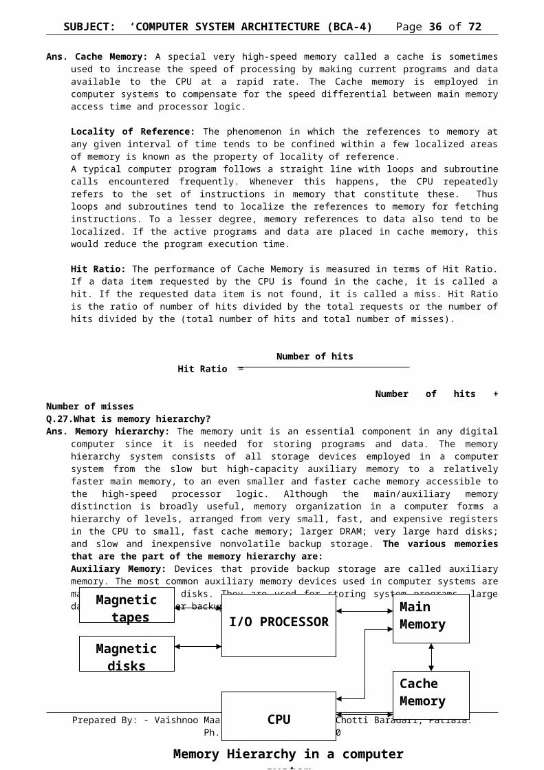
SUBJECT: ‘COMPUTER SYSTEM ARCHITECTURE (BCA-4) Page 36 of 57
Q.3.What is Multiplexer and Demultiplexer ? Explain the difference between the two?Ans.A multiplexer is a combinational circuit having many input lines and one output line. It is a combinational circuit that selects one to many input lines and directs it to a single output line. The selection of the input line is controlled by a set of selection lines. A multiplexer is also known as a data selector.
Design of 4: 1 Multiplexer: There are four data inputs, so we need two selection bits, S1 and S0..
S1 S0 Q
0 0 D0
0 1 D1
1 0 D2
1 1 D3
x x 1
TRUTH TABLE
Prepared By: - Vaishnoo Maa Computers, SCO 145, Chotti Baradari, Patiala.Ph. 0175-2205100, 2215100
S1 BLOCK S0 DIAGRAM
D3 4 : 1
D2 MUX
D1
D0
SUBJECT: ‘COMPUTER SYSTEM ARCHITECTURE (BCA-4) Page 37 of 57
CIRCUIT DIAGRAM OF 4 : 1 MULTIPLEXER
A demultiplexer is a circuit that receives information on a single line and transmits the information on one of 2n
possible output lines. The selection of a specific output line is controlled by the bit values of n selection lines. For eg. In a 2-to-4 demultiplexer, ,the input variable E has a path to all the four outputs,but the input information is directed to only one of the output lines, as specified by the binary values of A and B. The truth table, block-diagram and circuit-diagram of a 2-to-4 demultiplexer is shown below:
Truth –Table of 2-to-4 demultiplexerE A B D0 D1 D2 D3
0 0 0 0 1 1 10 0 1 1 0 1 10 1 0 1 1 0 10 1 1 1 1 1 0
Block-diagram Circuit-diagram
Q. 4. What is an encoder and decoder? Explain the difference between the two? Ans. A decoder is a combinational circuit that converts binary information form the ‘n’ coded inputs to a maximum of 2n unique outputs. For eg. In a 3- to- 8 line decoder, the three inputs are decoded into 8 outputs. Each output representing one of the minterms of the 3-input variables. A particular example of decoder includes binary to octal conversion. The truth-table and circuit diagram of a 3-to-8 decoder is shown below:
X Y Z D0 D1 D2 D3 D4 D5 D6 D7
Prepared By: - Vaishnoo Maa Computers, SCO 145, Chotti Baradari, Patiala.Ph. 0175-2205100, 2215100

SUBJECT: ‘COMPUTER SYSTEM ARCHITECTURE (BCA-4) Page 38 of 57
0 0 0 1 0 0 0 0 0 0 00 0 1 0 1 0 0 0 0 0 00 1 0 0 0 1 0 0 0 0 00 1 1 0 0 0 1 0 0 0 01 0 0 0 0 0 0 1 0 0 01 0 1 0 0 0 0 0 1 0 01 1 0 0 0 0 0 0 0 1 01 1 1 0 0 0 0 0 0 0 1
Truth-Table
Circuit-Diagram
An encoder has 2n input lines and n output lines. The output lines generate the binary code corresponding to the input value. In encoder, there are no selection lines.An Encoder is a digital circuit that performs the inverse operation of a decoder. An example of an encoder is the octal-to-binary encoder. The octal to binary encoder consists of 8 inputs ,one for each of the 8 digits and 3 outputs that generate the corresponding number. It is constructed with OR gates. The low order bit z is 1 if the input octal digit is odd. Output y is 1 for octal digits 2,3,6,7.Output x is 1 for octal digits 4,5,6,7.D0 is not connected to any OR gate as the binary output must be all 0’s in this case.
Truth-table of octal to binary encoder:
D0 D1 D2 D3 D4 D5 D6 D7 X Y Z1 0 0 0 0 0 0 0 0 0 00 1 0 0 0 0 0 0 0 0 10 0 1 0 0 0 0 0 0 1 00 0 0 1 0 0 0 0 0 1 10 0 0 0 1 0 0 0 1 0 00 0 0 0 0 1 0 0 1 0 10 0 0 0 0 0 1 0 1 1 00 0 0 0 0 0 0 1 1 1 1
Prepared By: - Vaishnoo Maa Computers, SCO 145, Chotti Baradari, Patiala.Ph. 0175-2205100, 2215100

SUBJECT: ‘COMPUTER SYSTEM ARCHITECTURE (BCA-4) Page 39 of 57
Circuit-Diagram of Octal to binary encoder
Q.5 What is a sequential and combinational circuit. Also give examples.Ans. Combinational Circuits: A combinational circuit is a connected arrangement of logic gates with a set of inputs and outputs. At any given time, the binary values of the outputs are a function of binary combination of the inputs. A combinational circuit performs a specific information-processing operation fully specified by a set of Boolean functions.
BLOCK DIAGRAM OF A COMBINATIONAL CIRCUIT
Multiplexer is an example of combinational circuit. is a combinational circuit having many input lines and one output line. It is a combinational circuit that selects one to many input lines and directs it to a single output line. The selection of the input line is controlled by a set of selection lines. A multiplexer is also known as a data selector.
Design of 4: 1 Multiplexer: There are four data inputs, so we need two selection bits, S1 and S0.. The circuit diagram of a 4:1 multiplexer is given below:
CIRCUIT DIAGRAM OF 4 : 1 MULTIPLEXER
Sequential Circuits: A sequential circuit is an interconnection of flip-flops and gates. The gates by themselves constitute a combinational circuit, but when included with the flip-flops, the overall circuit is classified as a sequential circuit. i.e. Sequential circuits employ memory elements in addition to logic
Prepared By: - Vaishnoo Maa Computers, SCO 145, Chotti Baradari, Patiala.Ph. 0175-2205100, 2215100
Combinational
Circuitn input variables
m output variables

SUBJECT: ‘COMPUTER SYSTEM ARCHITECTURE (BCA-4) Page 40 of 57
gates. The state of memory elements in turn is a function of previous inputs. As a consequence, the outputs of a sequential circuit depend not only on present inputs but also on past inputs.
BLOCK DIAGRAM OF A CLOCKED SEQUENTIAL CIRCUIT
Flip-flop is an example of a sequential circuit. A flip-flop can maintain a binary state indefinitely until directed by an input signal to switch states. The basic flip-flop can be constructed using NAND and NOR gates. The cross-couple connection from the output of one gate to the input of the other gate constitutes a feedback path. For this reason, these circuits are classified as sequential circuits. Each flip-flop has two inputs , set and reset and two outputs, Q and Q’. This type of flip=flop is sometimes called direct-coupled RS flip-flop or SR latch. The R and S are the first letters of the two input names. Below, the truth-table and circuit diagram of basic flip-flop using NOR gates is given. The output of a NOR-gate is 0 if any input is 1 and the output is 1 only when all inputs are 0.
Circuit Diagram of RS flip-flop
Q.6.What is an instruction format? What is the difference between zero-address, one-address, and two-address instructions?
Ans.An instruction format specifies the binary code for one of the instructions from the instruction set of the computer system. The instruction format is interpreted by the control unit and generates control functions according to the given format. An instruction code is represented using a rectangular box whose size is equal to the length of the instruction. This box is divided into three parts which are known as fields. The various fields in an instruction format are:
1) Opcode field- This is the operation code field which specifies the operation to be performed.
2) Address field- This designates the memory address or a processor register.
3) Mode field- This specifies the way the operand or the effective address is determined.
Instruction format length depends on the number of address fields in the instructions. The number of address fields in the instruction format of a computer in turn depends on the internal organization of its registers. There are three types of register organizations. These are:
Single accumulator organization General register organization Stack organization
Prepared By: - Vaishnoo Maa Computers, SCO 145, Chotti Baradari, Patiala.Ph. 0175-2205100, 2215100
CombinationalCircuit Memory
elements
Inputs Outputs

SUBJECT: ‘COMPUTER SYSTEM ARCHITECTURE (BCA-4) Page 41 of 57
1. Single accumulator organization: In single accumulator organization, all operations are performed in a single processor register called accumulator. The instructions in such computers consist of a single operand. The other operand is implied to be in the accumulator.
2. General Register organization: In computers with General register organization, there are more than one processor registers. The instructions in such cases refer to more than one register. For example ADD R1,R2,R3 implies add value in register R2 with value in register R3 and store the result in register R1. Therefore instruction length in such cases will be longer.
3. Stack Organization: In computers with Stack organization, a stack is used for storing operands on which operations need to be performed. PUSH and POP instructions will require a single operand.
Instructions to a CPU are of different kinds based on the number of operands they contain or require, to operate on. These are as follows:
1. Zero-address instruction: Zero address type of instructions does not contain any operand or operand address. The operand and addresses are implied. The instruction CLA is a 0-address instruction. CLA stands for clear accumulator. Here the instruction itself specifies that the operation “clear” is to be performed on accumulator.
2. One-address instruction: In this type of instruction, a single operand address is specified. The other operand lies in the accumulator and the result is also stored back in the accumulator. For example LDA A, STA A, ADD A, PUSH A are some of the one-address instructions.
3. Two-address instruction: In this type of instructions, addresses of two operands are specified. The result of the operation is stored in one of the given operand addresses. For example, MOV R1,R2 is an example of two address instruction.
Q.7. What is RISC and CISC architecture? What is the difference between the two?Ans.RISC is short for reduced instruction set computers. These processors have only a limited (few) number of computer instructions. RISC chips are relatively cheap to produce and debug. RISC processors run up to 70% faster than CISC processors. RISC processor consists of mainly register to register operations, with only simple load and store operations for memory access. Also very few addressing modes are used in RISC instructions. Following are the characteristics of the RISC processor:
1. Relatively few instructions are used.2. Fewer addressing modes are used.3. Memory access is limited to load & store the instructions.4. All operations done within register of CPU.5. Fixed length, easily decodable instruction format is used.6. Single cycle instruction execution is preferred.7. Hardware rather than micro-programmed control is used.8. Also, large no of registers in processor unit.9. Use instruction Pipeline.
CISC is complex instruction set computers. These processors have a large number of complex instructions. CISC chips are costly to produce and debug. CISC processors are slower than the RISC processors. The essential goal of CISC architecture is to attempt to provide a single machine instruction for each statement that is written in high level language. Another characteristic of CISC is the use of variable-length instruction format. Instructions in a typical CISC processor provide direct manipulation of operands residing in memory. The main characteristics of CISC architecture are as follows:1. Large no of instructions-typically from 100 to 250 instructions.2. Some instructions that perform specialized tasks and are used infrequently3. More number of addressing modes typically from 5 to 20 different modes.4. Uses variable length instruction formats.5. Uses instructions that manipulate operands in memory.
Difference between RISC and CISC could be enumerated as below:RISC CISCRISC stands for reduced instruction set computers
CISC stands for Complex Instruction Set Computers
RISC processor uses a small and simplified instruction set
CISC uses complex and large instruction set
Uses few addressing modes Uses a number of addressing modesUses fixed length instruction format Uses variable length instruction formatRISC architecture reduces the execution time of instructions by simplifying the instruction set
Each instruction performs low-level operations, hence the execution time is more
Prepared By: - Vaishnoo Maa Computers, SCO 145, Chotti Baradari, Patiala.Ph. 0175-2205100, 2215100

SUBJECT: ‘COMPUTER SYSTEM ARCHITECTURE (BCA-4) Page 42 of 57
Because of simplified instructions, the applications are easier to develop
Applications require effort to develop as complex operations are involved
Q.8 What are the different modes of data transfer?Ans. Binary information received from an external device is usually stored in memory for later processing.
Data transfer between the central computer and I/O devices may be handled in a variety of modes. Some modes use CPU as an intermediate path; others transfer the data directly to and from the memory unit. Data transfer to and from peripherals may be handled in one of the three possible modes: Programmed I/O Interrupt-initiated I/O Direct Memory Access (DMA)
1. Programmed I/O: Programmed I/O operations are the result of I/O instructions written in the computer program. Each data transfer is initiated by an instruction in the program. Usually, the transfer is to and from a CPU register and peripheral. Other instructions are needed to transfer the data to and from CPU and memory. Transferring data under program control requires constant monitoring of the peripheral by the CPU. Once a data transfer is initiated, the CPU is required to monitor the interface to see when a transfer can again be made. It is up to the programmed instructions executed in the CPU to keep close tabs on everything that is taking place in the interface unit and the I/O device.
2. Interrupt Initiated I/O: In the programmed I/O method, the CPU stays in a program loop until the I/O unit indicates that it is ready for data transfer. This is a time consuming process since it keeps the processor busy needlessly. It can be avoided by using an interrupt facility and special commands to inform the interface to issue an interrupt request signal when the data are available from the device. In the meantime the CPU proceeds to execute another program. The interface meanwhile keeps monitoring the device. When the interface determines that the device is ready for data transfer, it generates an interrupt request to the computer. Upon detecting the external interrupt signal, the CPU momentarily stops the task it is processing, branches to a service program to process the I/O transfer, and the returns to the task it was originally performing.
3. Direct Memory Access (DMA): Transfer of data under programmed I/O is between CPU and peripheral. In direct memory access (DMA), the interface transfers the data into and out of the memory unit through the memory bus. The CPU initiates the transfer by supplying the interface with the starting address and the number of words needed to be transferred and then proceeds to execute other tasks. When the transfer is made, the DMA requests memory cycles through the memory bus. When the request is granted by the memory controller, the DMA transfers the data directly into the memory. The CPU merely delays its memory access operation to allow the direct memory I/O transfer
Q.9. How can NAND and NOR be considered as universal gates? Ans. A universal gate is a gate which can implement any Boolean function without need to use any other gate type. The NAND and NOR gates are universal gates. In practice, this is advantageous since NAND and NOR gates are economical and easier to fabricate and are the basic gates used in all IC digital logic families.
NAND Gate is a Universal Gate: To prove that any Boolean function can be implemented using only NAND gates, we will show that the AND, OR, and NOT operations can be performed using only these gates.Implementing an Inverter Using only NAND Gate The figure shows the way in which a NAND gate can be used as an inverter (NOT gate).
All NAND input pins connect to the input signal A gives an output A’.
Implementing AND Using only NAND Gates An AND gate can be replaced by NAND gates as shown in the figure (The AND is replaced by a NAND gate with its output complemented by a NAND gate inverter).
Implementing OR Using only NAND Gates
Prepared By: - Vaishnoo Maa Computers, SCO 145, Chotti Baradari, Patiala.Ph. 0175-2205100, 2215100

SUBJECT: ‘COMPUTER SYSTEM ARCHITECTURE (BCA-4) Page 43 of 57
An OR gate can be replaced by NAND gates as shown in the figure (The OR gate is replaced by a NAND gate with all its inputs complemented by NAND gate inverters).
Thus, the NAND gate is a universal gate since it can implement the AND, OR and NOT functions.
NOR Gate is a Universal Gate: To prove that any Boolean function can be implemented using only NOR gates, we will show that the AND, OR, and NOT operations can be performed using only these gates. Implementing an Inverter Using only NOR Gate
The figure shows the way in which a NOR gate can be used as an inverter (NOT gate).
All NOR input pins connect to the input signal A gives an output A’.
Implementing OR Using only NOR Gates An OR gate can be replaced by NOR gates as shown in the figure (The OR is replaced by a NOR gate with its output complemented by a NOR gate inverter)
Implementing AND Using only NOR Gates An AND gate can be replaced by NOR gates as shown in the figure (The AND gate is replaced by a NOR gate with all its inputs complemented by NOR gate inverters)
Thus, the NOR gate is a universal gate since it can implement the AND, OR and NOT functions.
Q.10. What is RAM? What is the difference between static and dynamic RAM?Ans.RAM was used to refer to a random-access memory but now it is used to designate read/write memory.
RAM is volatile, that is the contents stored in RAM, remain only as long as power is available to the system. Once, the power is taken off, the contents get deleted. Any program to be executed, has to be in RAM. The block diagram of RAM is as shown below:
CS1 (CS2)’
RD 8-bit data bus WR 7-bit address
A RAM chip allows data to be accessed in a random manner. It provides a bi-directional bus, that transfers data from main memory to CPU and vice-versa. RAM chips are available as 126 * 6 chips. The chip shown above is 128* 8 chip. Its capacity is 128 words of 8 bits each. This requires a 7-bit
Prepared By: - Vaishnoo Maa Computers, SCO 145, Chotti Baradari, Patiala.Ph. 0175-2205100, 2215100
128 X 8 RAM

SUBJECT: ‘COMPUTER SYSTEM ARCHITECTURE (BCA-4) Page 44 of 57
address and an 8-bit bi-directional bus. The read and write inputs specify the memory operation and the two chip-select control Inputs(CS) are for enabling the chip only when it is selected by the microprocessor. Two control inputs are provided to facilitate the decoding of the address lines when multiple chips are used. The unit is operational only when CS1=1 and (CS2)’ =0. If the select inputs are enabled but read/write are disabled the memory is inhibited and the data-bus is in a high-impedance state. When write input is enabled, the memory stores a byte from the data-bus into a location specified by the input lines. And when read input is enabled, the content of the selected byte is placed into the data-bus.
The two common types of RAM are static RAM (SRAM) and dynamic RAM (DRAM).
SRAM is a semi-conductor memory that retains its contents as long as power is supplied to it. The memory locations can be accessed, that is written or read any order regardless of the memory location accessed before. These are high-speed memories. The term static is used because no periodic clock signals are required to retain stored data indefinitely. SRAM can be designed using either the bipolar or MOS technology.DRAM is a semi-conductor memory that uses capacitors to store each data bit. The quantity of charge stored in a capacitor determines whether the stored bit is 0 or 1. The capacitor needs to be periodically refreshed to avoid the leakage of charge from the capacitor.
DRAM has the disadvantage that the capacitor cannot retain the charge for long periods and requires refreshing circuitry. Thus this process requires additional circuitry and creates design problems. However, it is denser and cheaper than SRAM because of the presence of simple memory cells.
Q.11. What is ROM? What are the different types of ROM? Ans. ROM is referred to Read-Only memory. It is used to store data permanently as the data once written in
this memory cannot be modified. It is used to store firmware which is a kind of software that does not need to be modified in the future.
ROM chips have two select inputs, the address line and a data-bus which is unidirectional as writing is not possible on a ROM chip. ROM cells are manufacture using MOS technology. The block-diagram of ROM is as shown below:
CS1 (CS2)’ 8-bit data bus
9-bit address
ROM is of the following types:1. Mask ROM- It is also called ROM. It allows the performance of only read operation. Data is stored
in it during chip fabrication and the data once written, cannot be changed. 2. Programmable ROM (PROM)- It can be programmed only once. PROM chips have a grid of rows
and columns with a fuse connecting the intersection between them. When current flows through a column, it goes through the fuse in the cell and stores the value 1. All the memory cells have a fuse, so the initial state of a PROM chip contains all 1s. Inorder to change the value of a cell to 0, the programmer needs to send a specific amount of current to the cell. The higher voltage breaks the connection between the column and the row by burning out the fuse. This is known as burning the PROM.
3. Erasable Programmable ROM(EPROM)- This type of ROM can be reprogrammed by erasing the existing data in the memory cells. They can be reprogrammed many times as per the requirement of the user. EPROMS have a disadvantage that incremental changes cannot be stored on the chip. The entire chip has to be erased even for making a change to the portion of the chip. EPROM is further of two types:
a. Electrically Erasable Programmable Read Only Memory (EEPROM)- In this type of ROM, programming as well as erasing is achieved through electrical pulses. Flash memory is a type of EEPROM. EEPROM chips do not have to be removed for reprogramming and erasure of entire chip is not needed to change a specific portion of it. Also additional equipments are not needed for changing the contents of this chip.
b. Ultra Violet Programmable Read Only Memory(UVPROM)- In this type of ROM, the contents are erased using ultra violet rays. The ultra-violet light is passed through a window
Prepared By: - Vaishnoo Maa Computers, SCO 145, Chotti Baradari, Patiala.Ph. 0175-2205100, 2215100
512 X 8 ROM

SUBJECT: ‘COMPUTER SYSTEM ARCHITECTURE (BCA-4) Page 45 of 57
into the IC-package containing the chip. The light releases the charge stored in the cell. As a result the contents of the chip get erased.
Q.12. What is the difference between handshaking and strobe?Ans.When two units wanting to communicate with each other, have an internal timing, independent from each
other, the two units are said to be asynchronous to each other. This type of data–transfer requires that control signals be transmitted between the communicating units to indicate the time at which the data is being transmitted. The two methods used for this purpose are: strobe control and handshaking.
Strobe control method-In this method, a single control line is used to time each transfer.The strobe may be activated by either the source or the destination unit.
Prepared By: - Vaishnoo Maa Computers, SCO 145, Chotti Baradari, Patiala.Ph. 0175-2205100, 2215100

SUBJECT: ‘COMPUTER SYSTEM ARCHITECTURE (BCA-4) Page 46 of 57
The figure below shows source-initiated strobe for data transfer.
The data bus is used to carry the data from source to destination and strobe is a single line that informs when a valid data word is available on the bus. The source unit first places the data on the data bus. After a brief delay to ensure that the data settle to a steady value, the source activates the strobe-pulse. The information on the data-bus and the strobe-signal remain in active-state for a sufficient time-period to allow the destination to receive data. Often, the destination unit, uses the falling edge of the strobe pulse to transfer the contents of the data-bus into one of its internal registers. The source removes the data from the bus a brief period after it disables it strobe pulse. Infact, the source does not remove the data from the bus; the fact that the strobe signal is disabled indicates that the data-bus does not carry valid data. New valid data is available only when the strobe is activated again.
In many computers, the read operation is initiated by the destination. It informs the source to place a selected word into the data bus. The destination initiated strobe for data transfer is as shown below:
Handshaking method-It is one of the methods used in Asynchronous data transfer. In this method, the
data is transferred by source only when the receiving device is ready to accept the data. The status of devices is checked by special control signals.
. Each data item is transferred with a control signal that indicates the presence of data in a bus. The unit receiving the data item responds with another control signal to acknowledge receipt of the data. This type of agreement between two independent units is referred to as handshaking.
The block-diagram of source-initiated transfer using handshaking, is as shown below:
The source initiates the transfer by placing the data on the bus and enabling its data-valid signal. The data-accepted signal is activated by the destination unit after is accepts data from the bus. The source-unit then disables its data-valid signal which invalidates the data on the bus. The destination unit then disables its data
Prepared By: - Vaishnoo Maa Computers, SCO 145, Chotti Baradari, Patiala.Ph. 0175-2205100, 2215100
Source Unit
Destination Unit
Data bus
Data valid
Data Accepted
Data bus
SourceDestination
Strobe
Data busSource
Destination
Strobe

SUBJECT: ‘COMPUTER SYSTEM ARCHITECTURE (BCA-4) Page 47 of 57
accepted signal and the system goes into the initial state. Only after the data accepted signal is disabled by the destination, the source sends new data.
In the destination-initiated data transfer, the source unit does not place data on the data bus until it receives ‘ready for data ‘ signal from the destination unit. From there-on, the handshaking procedure follows the same pattern as in the source-initiated case. The block-diagram for destination-initiated data transfer using handshaking, is as shown below:
Q.13.What is cache Memory? Discuss its mapping schemes.Ans. When over a short interval of time the address generated by a typical program refers to a few localized areas of memory repeatedly, while remainder of memory is accessed relatively infrequently. So, repeatedly required data are placed in fast small memory, which decreases average memory access time i.e. it reduces total execution time of the program. Such a fast small memory is called Cache memory. Placed between the CPU & main memory.
The transformation of data from main memory to cache memory is called mapping & various mapping schemes are as follows: Associative Mapping Direct mapping Set-associative memory
Associative memory: - Stores both the address & content (data) of the memory word. It permits any location in Cache to store any word from main memory.Diagram shows three words presently stored in cache. A CPU address of 15 bits placed in argument register & its associative memory is searched for a matching address. If the address is found, corresponding 12-bit data is read & sent to CPU. If no match is found, then main memory is accessed for the word. The address-data pair is then transferred to associative memory. If cache is full, then address-data pair must be displaced to make room for a pair that is needed & not presently in cache memory.
Prepared By: - Vaishnoo Maa Computers, SCO 145, Chotti Baradari, Patiala.Ph. 0175-2205100, 2215100
Source Unit
Destination Unit
Data bus
Data valid
Ready for data
10001 3450
27770 6710
22345 1234
CPU address (15 bits)
Address Data
Argument register
Associative Mapping

SUBJECT: ‘COMPUTER SYSTEM ARCHITECTURE (BCA-4) Page 48 of 57
Direct mapping: - Associative memories are expensive as compared to random-access memories because of the added logic associated with each cell. In this method CPU address of 15 bits is divided into two fields. The nine least significant bits constitute the index field and the remaining six bits form the tag field. The figure shows that main memory needs an address that includes both the tag and the index bits. The number of bits in the index field is equal to the number of address bits required to access the cache memory. In the general case, there are 2 k words in cache memory and 2n words in main memory. The n-bit memory address is divided into two fields: k bits for the index field and n-k bits for the tag field. The direct mapping cache organization uses the n-bit address to access the main memory and the k-bit index to access the cache. The diagram below shows direct mapping:
Set-Associative mapping: - This mapping technique is an improvement over the direct mapping organization in that each word of cache can store two or more words of memory under the same index address. Each data word is stored together with its tag and total number of tags. Data items in one word of cache is set to form a set. Example of set associative cache organization for a set size of two is
Prepared By: - Vaishnoo Maa Computers, SCO 145, Chotti Baradari, Patiala.Ph. 0175-2205100, 2215100
000
OctalAddress
6 Bit 9 bit
000
77777
OctalAddress
00
Tag Index
32K X 12
Main memory
Address = 15 bitsData = 12 bits
512 X 12
Cache memory
Address = 9 bitsData = 12 bits
Direct Mapping Scheme
777

SUBJECT: ‘COMPUTER SYSTEM ARCHITECTURE (BCA-4) Page 49 of 57
shown in the figure below:
Q.14. a) State the rules of Boolean Algebra. State and prove one of the De Morgan laws. b) Draw the circuit diagram for the following Boolean expression:
Ans. Boolean algebra deals with binary values and logical operators: AND, OR, NOT. Boolean algebra was give by George Boole. It can also be called algebra of logic. The various laws and rules of Boolean Algebra are as follows:
Properties of 0 and 1: a. 0+X=X b: 1+ X=1
c: 0. X=0 d: 1. X=X Idempotence Law: This law states that:
a: X+X=X b: X . X=X
Law of Involution: This law state that: (X’)’=X
Complementarity law: This law states that: a: X + X’=1 b: X . X’=0 Commutative law: This law states that: a: X+Y=Y+X
b: X . Y=Y. X Associative law : This law states that: a: X +(Y+Z) =(X+Y) +Z b: X(YZ)=((XY)Z Distributive law: This law states that:: a: X(Y+Z)=XY+XZ b: X+YZ=(X+Y)(X+Z)Law of Absorption: this law states that: a: X+XY=X b: X(X+Y)=X
De Morgan’ s law: This law states that: a: (X+Y)’=X’ Y’ b: (X.Y)’=X’+ Y’Proving the first law: (X+Y)’=X’Y’. To prove this law, we use complementarity laws. Let us assume that P=X+Y where P,X,Y are logic variables. Then according to complementarity law: P+P’=1 and P.P’=0This means that if P,X,Y are Boolean variables then this complementarity law must hold for variable P. In other words, if P’ i.e. if (X+Y)’=X’Y’ then: (X+Y) +X’Y’ must be equal to 1 and (X+Y). (X’Y’) must be equal to 0
Prepared By: - Vaishnoo Maa Computers, SCO 145, Chotti Baradari, Patiala.Ph. 0175-2205100, 2215100
01 3450 02 5670
02 6710 00 2340
000
Index Tag Data Tag Data
Two-Way Associative Cache Mapping
777
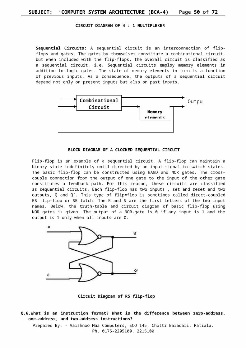
SUBJECT: ‘COMPUTER SYSTEM ARCHITECTURE (BCA-4) Page 50 of 57
Let us first prove the first part, i.e.(X+Y) +(X’Y’) =1(X+Y) + (X’Y’) = ((X+Y)+X’) ((X+Y)+Y’) …. acc. to distributive law = (X+X’+Y) (X+Y+Y’) = (1+Y) (X+1) …… as X+X’=1 =1.1 =1 (hence first part is proved)
Now, to prove the second part: (X+Y) .X’Y’=0 (X+Y).X’Y’=X’Y’(X+Y) = X’Y’X + X’Y’Y =XX’Y’ + X’YY’ =0.Y’ +X’. 0 =0+0=0 (thus proving the second part)
Thus: (X+Y)’ =X’Y’ Q.15. Explain the working of basic flip-flop.Ans. A flip-flop is an asynchronous sequential circuit. The basic flip-flop is also known as RS flip-flop or SR latch. R and S are the first characters of the two inputs viz. Reset and Set. This flip-flop can be constructed using NOR gate or NAND gate.
Using Nor gate, the working of this flip-flop is as explained below: If the set input is 1 and reset input is 0, since gate 2 has an input of 1, the output Q’ must be 0,which puts both inputs at gate 1 at 0, so that output Q is 1. When the set input is returned to 0, the outputs remain the same, because output Q remains 1 , leaving one input of gate 2 at 1. This causes output Q’ to stay at 0,which leaves both inputs at gate 1 at 0,so that output Q is 1. In the same manner it is possible to show that a 1 in the reset input changes output Q to 0 and Q’ to 1. When the reset input returns to 0, the outputs do not change.
When a 1 is applied to both the set and reset inputs, both Q and Q’ outputs go to 0. This condition violates the fact that outputs Q and Q’ are complements of each other. In normal operation this condition must be avoided by making sure that 1’s are not applied to both inputs simultaneously.A flip-flop has two useful states. When Q =1 and Q’=0,it is the set state. And when Q=0 and Q’=1, it is the clear state.
Under normal operation, both inputs remain at 0 and the application of a momentary 1 to the set input causes the flip-flop to go to the set state. The set input must go back to 0 before a 1 is applied to the reset input. A momentary 1 applied to the reset input causes the flip-flop to go to clear state. When a 1 is applied to set as well as reset inputs, both Q and Q’ become 0 ,making this state undefined which should usually be avoided. If both inputs now go to 0, the state of the flip-flop is indeterminate.The truth-table and circuit diagram for RS flip-flop is as shown below:
Prepared By: - Vaishnoo Maa Computers, SCO 145, Chotti Baradari, Patiala.Ph. 0175-2205100, 2215100
SUBJECT: ‘COMPUTER SYSTEM ARCHITECTURE (BCA-4) Page 51 of 57
The RS flip-flop using NAND gates, operates with both inputs normally at 1. A momentary 0 at the set input, causes Q to go to 1 and Q’ to go to 0, thus putting the flip-flop in the set state. After the set input returns to 1, a momentary 0 to reset input causes the flip-flop go to clear state. When both inputs go to 0, both outputs become 1 which is the state normally avoided. An RS flip-flop using NAND gates is as shown below:
circuit diagram using NAND gates
S R Q Q’1 0 0 11 1 0 10 1 1 01 1 1 00 0 1 1 Truth-Table
Q.16. Explain the following : a) General Register Organizationb) Stack OrganizationAns. In the General Register CPU Organization, there are more than one registers in the CPU. The registers communicate with each other not only for data transfers but also while performing various micro-operations. Hence a better efficiency is achieved when they are connected with a common bus system. Suppose there is a bus-organization for seven CPU registers, as shown in the diagram below. The output of each register is connected to two multiplexers(MUX) to form the two buses A and B. The selection lines in each MUX select one register for the particular bus. The A and B buses form the inputs to a common ALU. The
Prepared By: - Vaishnoo Maa Computers, SCO 145, Chotti Baradari, Patiala.Ph. 0175-2205100, 2215100

SUBJECT: ‘COMPUTER SYSTEM ARCHITECTURE (BCA-4) Page 52 of 57
operation selected in the ALU determines the micro-operation to be performed. The result of the micro-operation is available for output data and also goes into the inputs of all registers. The register that receives the information from the output bus is selected by a decoder.
The stack in digital computers is essentially a memory unit with an address register that can count. The register that hold the address for the stack is called stack pointer (SP) as its value always points to the top item in the stack. The two operations of a stack are insertion and deletion of items. The operation of insertion is called push and the operation of deletion is called pop.
A stack can be placed in a portion of a large memory or it can be organized as a collection of finite number of memory words or registers. In the following figure, the organization of 64-word register stack is shown:
63
3 2
AA 1 0
Three items are placed in the stack: A, B and C. SP is incremented each time. Item C is on the top and since it’s the third item, SP contains 3. When pop operation is performed, the memory-word at address 3 is read which is C and SP is decremented to 2. Now SP points to memory word containing B.
In a 64-word stack, the SP contains 6 bits because 26 =64. Since SP has only 6 bits, it cannot exceed a number greater than 63(111111 in binary), When 63 is incremented by1, the result is 0 since 111111+1 =1000000. But SP can accommodate only the 6 least significant bits so it contains 000000 and becomes 0. Hence SP starts pushing values from memory word 1 and the last value is pushed onto memory-word 0. Similarly in pop operation, when 000000 is decremented by 1, it becomes 111111, i.e. 63. Hence in pop operation, the SP will start from 0, is decremented and in this process when it again reaches the value 0, it becomes empty. The one-bit register FULL is set to 1 when the stack is full, i.e. when SP is 0. And the one-bit EMPTY register is set to 1 when stack is empty. DR is data-register that holds the data to be pushed onto the stack.The push operation is implemented with the following sequence of micro-operations:SP←SP +1 increment stack pointerM[SP]←DR write item onto the top of the stackif(SP=0) then (FULL←1) check if stack is fullEMPTY←0 mark the stack as not empty
The pop operation is implemented with the following sequence of micro-operations:DR←M [SP] read item from the top of the stackSP←SP-1 decrement stack pointer
Prepared By: - Vaishnoo Maa Computers, SCO 145, Chotti Baradari, Patiala.Ph. 0175-2205100, 2215100
B A DR
SP
FULL EMPTY
C

SUBJECT: ‘COMPUTER SYSTEM ARCHITECTURE (BCA-4) Page 53 of 57
if (SP=0) then (EMPTY←1) check if stack is emptyFULL←0 mark the stack as- not full
Q.17. What is the difference between hardwired and micro-programmed control unit?Ans.The Hard-Wired Control Unit
The following figure is a block diagram showing the internal organization of a hard-wired control unit for a simple computer:
Input to the controller consists of the 4-bit opcode of the instruction currently contained in the Instruction Register and the negative flag from the accumulator. The controller's output is a set of 16 control signals that go out to the various registers and to the memory of the computer, in addition to a HLT signal that is activated whenever the leading bit of the op-code is one. The controller is composed of the following functional units: A ring counter, an instruction decoder, and a control matrix.
The ring counter provides a sequence of six consecutive active signals that cycle continuously. Synchronized by the system clock, the ring counter first activates its T0 line, then its T1 line, and so forth. After T5 is active, the sequence begins again with T0
The instruction decoder takes its four-bit input from the op-code field of the instruction register and activates one of its 8 output lines. Each line corresponds to one of the instructions in the computer's instruction set.
The most important part of the hard-wired controller is the control matrix. It receives input from the ring counter and the instruction decoder and provides the proper sequence of control signals.
In the case of a hard-wired control unit the control matrix is responsible for sending out the required sequence of signals.
An alternative way of generating the control signals is that of micro-programmed control. In a micro-programmed control unit, the binary control variables are stored in memory. Each word in the control memory contains a micro-instruction. The micro-instruction specifies one or more micro-operations for the system. A sequence of micro-instructions constitutes a micro-program. Each bit of a microinstruction might correspond to one control signal. If the bit is set it means that the control signal will be active; if cleared the signal will be inactive. Execution of a machine language instruction could then be caused by fetching the proper sequence of microinstructions from the control memory and sending them out to the data path section of the computer.
Prepared By: - Vaishnoo Maa Computers, SCO 145, Chotti Baradari, Patiala.Ph. 0175-2205100, 2215100

SUBJECT: ‘COMPUTER SYSTEM ARCHITECTURE (BCA-4) Page 54 of 57
The following figure is a block diagram of a micro-programmed control unit.
The heart of the controller is the control 32 X 24 ROM memory in which up-to 32 24-bit long microinstructions can be stored. Each is composed of two main fields: a 16-bit wide control signal field and an 8-bit wide next-address field. Each bit in the control signal field corresponds to one of the control signals. The next-address field contains bits that determine the address of the next microinstruction to be fetched from the control ROM. Words selected from the control ROM feed the microinstruction register. This 24-bit wide register is analogous to the outer machine's instruction register. Specifically, the leading 16 bits (the control-signal field) of the microinstruction register are connected to the control-signal lines that go to the various components of the external machine's data path section.
Addresses provided to the control ROM come from a micro-counter register, which is analogous to the external machine's program counter. The micro-counter, in turn, receives its input from a multiplexer which selects from : (1) the output of an address ROM, (2) a current-address incrementer, or (3) the address stored in the next-address field of the current microinstruction. The controller's address ROM is fed by the outer computer's instruction register.
The address ROM maps the op-code of the instruction currently contained in the op-code field of the instruction register to the starting address of the corresponding micro-program in the control ROM.
Differences between hardwired control and micro-programmed control unit are mentioned through the table below:Factors Micro-programmed Control
unitHardwired Control unit
Flexibility It is more flexible as it is made of micro-programs that are easy to change
It is made of combinational circuits with physical connections. Modifications in these circuits is difficult
Speed of execution It is less as micr-programs take more time to generate control signals
It generates control signals faster. So, speed is faster.
Implementation Micro-programs are easy to design
Hardwired circuits are difficult to design
Q.18 What is auxiliary memory? Explain various types of auxiliary memory.
Prepared By: - Vaishnoo Maa Computers, SCO 145, Chotti Baradari, Patiala.Ph. 0175-2205100, 2215100

SUBJECT: ‘COMPUTER SYSTEM ARCHITECTURE (BCA-4) Page 55 of 57
Ans. Auxiliary memory holds programs and data for future use, and, because it is nonvolatile (like ROM), it is used to store inactive programs and to archive data. Early forms of auxiliary storage included punched paper tape, punched cards, and magnetic drums. Since the 1980s, the most common forms of auxiliary storage have been magnetic disks, magnetic tapes, and optical discs. The efficiency of auxiliary memory is determined by the following factors:
Access time- It refers to the average time taken in reaching at the memory location and obtaining the data.Seek time- It refers to the time that is taken by the head to reach at the desired location in the disk.Transfer rate- It refers to the amount of data transferred in a unit time.Capacity and cost- It determines the efficiency of the auxiliary memory.The common types of auxiliary memory are as explained below:
Magnetic disks are coated with a magnetic material such as iron oxide. There are two types: hard disks made of rigid aluminum or glass, and removable diskettes made of flexible plastic. Since the invention of the floppy disk drive (FDD) at IBM, diskettes have shrunk from 8 inches (about 20 cm) to the current standard of 3.5 inches (about 8.9 cm). FDDs have low capacity—generally less than two megabytes—and have become obsolete since the introduction of optical disc drives in the 1990s.
Hard drives generally have several disks, or platters, with an electromagnetic read/write head for each surface. A microprocessor in the drive controls the motion of the heads and also contains RAM to store data for transfer to and from the disks. The heads move across the disk surface as it spins up to 15,000 revolutions per minute; the drives are hermetically sealed, permitting the heads to float on a thin film of air very close to the disk’s surface. A small current is applied to the head to magnetize tiny spots on the disk surface for storage; similarly, magnetized spots on the disk generate currents in the head as it moves by, enabling data to be read. FDDs function similarly, but the removable diskettes spin at only a few hundred revolutions per minute.
Magnetic tape, similar to the tape used in tape recorders, has also been used for auxiliary storage, primarily for archiving data. Tape is cheap, but access time is far slower than that of a magnetic disk because it is sequential-access memory—i.e., data must be sequentially read and written as a tape is unwound, rather than retrieved directly from the desired point on the tape.
Another form of auxiliary memory is the optical compact disc, developed from videodisc technology during the early 1980s. Data are recorded as tiny pits in a single spiral track on plastic discs that range from 3 to 12 inches (7.6 to 30 cm) in diameter, though a diameter of 4.8 inches (12 cm) is most common. The pits are produced by a laser or by a stamping machine and are read by a low-power laser and a photocell that generates an electrical signal from the varying light reflected from the pattern of pits. Optical discs are removable and have a far greater memory capacity than diskettes; the largest ones can store many gigabytes of information.
A common optical disc is the CD-ROM (compact disc read-only memory). It holds about 700 megabytes of data, recorded with an error-correcting code that can correct bursts of errors caused by dust or imperfections. CD-ROMs are used to distribute software, encyclopaedias, and multimedia text with audio and images. CD-R (CD-recordable), or WORM (write-once read-many), is a variation of CD-ROM on which a user may record information but not subsequently change it. CD-RW (CD-rewritable) disks can be re-recorded. DVDs (digital video, or versatile, discs), developed for recording movies, store data more densely than does CD-ROM, with more powerful error correction. Though the same size as CDs, DVDs typically hold 5 to 17 gigabytes—several hours of video or several million text pages.
Magneto-optical discs are a hybrid storage medium. In reading, spots with different directions of magnetization give different polarization in the reflected light of a low-power laser beam. In writing, every spot on the disk is first heated by a strong laser beam and then cooled under a magnetic field, magnetizing every spot in one direction, to store all 0s. The writing process then reverses the direction of the magnetic field to store 1s where desired.
Q.19. What is a counter. Explain the difference between synchronous and asynchronous counters.Ans. A counter is a sequential circuit which is made up of a set of flip-flops. The flip-flops count the number of times an event occurs. The flip flops in counters can count from 0 to N in binary system or BCD. Counters can be implemented using J-K flip-flops. They are broadly classified into synchronous and asynchronous counters.
With the Synchronous Counter, the external clock signal is connected to the clock input of every individual flip-flop within the counter so that all of the flip-flops are clocked together simultaneously (in parallel) at the
Prepared By: - Vaishnoo Maa Computers, SCO 145, Chotti Baradari, Patiala.Ph. 0175-2205100, 2215100
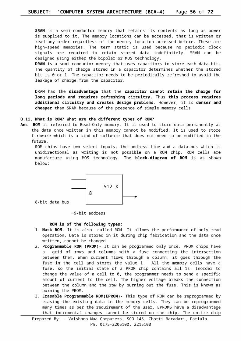
SUBJECT: ‘COMPUTER SYSTEM ARCHITECTURE (BCA-4) Page 56 of 57
same time giving a fixed time relationship. In other words, changes in the output occur in "synchronization" with the clock signal. This results in all the individual output bits changing state at exactly the same time in response to the common clock signal with no ripple effect and therefore, no propagation delay.
Binary 4-bit Synchronous Counter
It can be seen that the external clock pulses (pulses to be counted) are fed directly to each J-K flip-flop in the counter chain and that both the J and K inputs are all tied together in toggle mode, but only in the first flip-flop, flip-flop A (LSB) are they connected HIGH, logic "1" allowing the flip-flop to toggle on every clock pulse. Then the synchronous counter follows a predetermined sequence of states in response to the common clock signal, advancing one state for each pulse.
The J and K inputs of flip-flop B are connected to the output "Q" of flip-flop A, but the J and K inputs of flip-flops C and D are driven from AND gates which are also supplied with signals from the input and output of the previous stage. If we enable each J-K flip-flop to toggle based on whether or not all preceding flip-flop outputs (Q) are "HIGH" we can obtain the same counting sequence as with the asynchronous circuit but without the ripple effect, since each flip-flop in this circuit will be clocked at exactly the same time. As there is no propagation delay in synchronous counters because all the counter stages are triggered in parallel the maximum operating frequency of this type of counter is much higher than that of a similar asynchronous counter.
In asynchronous counters on the other hand , only the first flip-flop is clocked by an external clock. All subsequent flip-flops are clocked by the output of the preceding flip-flop. Asynchronous counters are slower than synchronous counters because of the delay in the transmission of the pulses from flip-flop to flip-flop. Asynchronous counters are also called ripple-counters because of the way the clock pulse ripples it way through the flip-flops.
Prepared By: - Vaishnoo Maa Computers, SCO 145, Chotti Baradari, Patiala.Ph. 0175-2205100, 2215100

SUBJECT: ‘COMPUTER SYSTEM ARCHITECTURE (BCA-4) Page 57 of 57
Binary 3-bit Asynchronous Counter
The above figure shows a 3-bit asynchronous counter made of three J-K flip-flops: A,B and C. For flip-flop A, the clock provides external input signals. The output of the flip-flop A is used as the clock input for the flip-flop B and so on. The flip-flop A triggers the flip-flop B and the flip-flop B triggers the flip-flop C. Before triggering the next flip-flop in the circuit, the present flip-flop needs to change its state.
Prepared By: - Vaishnoo Maa Computers, SCO 145, Chotti Baradari, Patiala.Ph. 0175-2205100, 2215100
Related Documents