© 2007 Microchip Technology Inc. DS70249A-page 28-1 Analog-to-Digital Converter (ADC) without DMA 28 Section 28. Analog-to-Digital Converter (ADC) without DMA HIGHLIGHTS This section of the manual contains the following major topics: 28.1 Introduction .................................................................................................................. 28-2 28.2 Control Registers ......................................................................................................... 28-4 28.3 Sample Conversion Sequence .................................................................................. 28-12 28.4 ADC Configuration ..................................................................................................... 28-19 28.5 ADC Interrupt Generation .......................................................................................... 28-23 28.6 Analog Input Selection for Conversion....................................................................... 28-24 28.8 Analog-to-Digital Sampling Requirements ................................................................. 28-31 28.9 Transfer Function ....................................................................................................... 28-33 28.10 Special Function Registers ........................................................................................ 28-35 28.11 Design Tips ................................................................................................................ 28-36 28.12 Related Application Notes.......................................................................................... 28-37 28.13 Revision History ......................................................................................................... 28-38

Welcome message from author
This document is posted to help you gain knowledge. Please leave a comment to let me know what you think about it! Share it to your friends and learn new things together.
Transcript

Section 28. Analog-to-Digital Converter (ADC) without DMA
Analog-to-D
igital C
onverter (AD
C)
without D
MA
28
HIGHLIGHTSThis section of the manual contains the following major topics:
28.1 Introduction .................................................................................................................. 28-228.2 Control Registers ......................................................................................................... 28-428.3 Sample Conversion Sequence .................................................................................. 28-1228.4 ADC Configuration ..................................................................................................... 28-1928.5 ADC Interrupt Generation .......................................................................................... 28-2328.6 Analog Input Selection for Conversion....................................................................... 28-2428.8 Analog-to-Digital Sampling Requirements ................................................................. 28-3128.9 Transfer Function ....................................................................................................... 28-3328.10 Special Function Registers ........................................................................................ 28-3528.11 Design Tips ................................................................................................................ 28-3628.12 Related Application Notes.......................................................................................... 28-3728.13 Revision History ......................................................................................................... 28-38
© 2007 Microchip Technology Inc. DS70249A-page 28-1
PIC24H Family Reference Manual
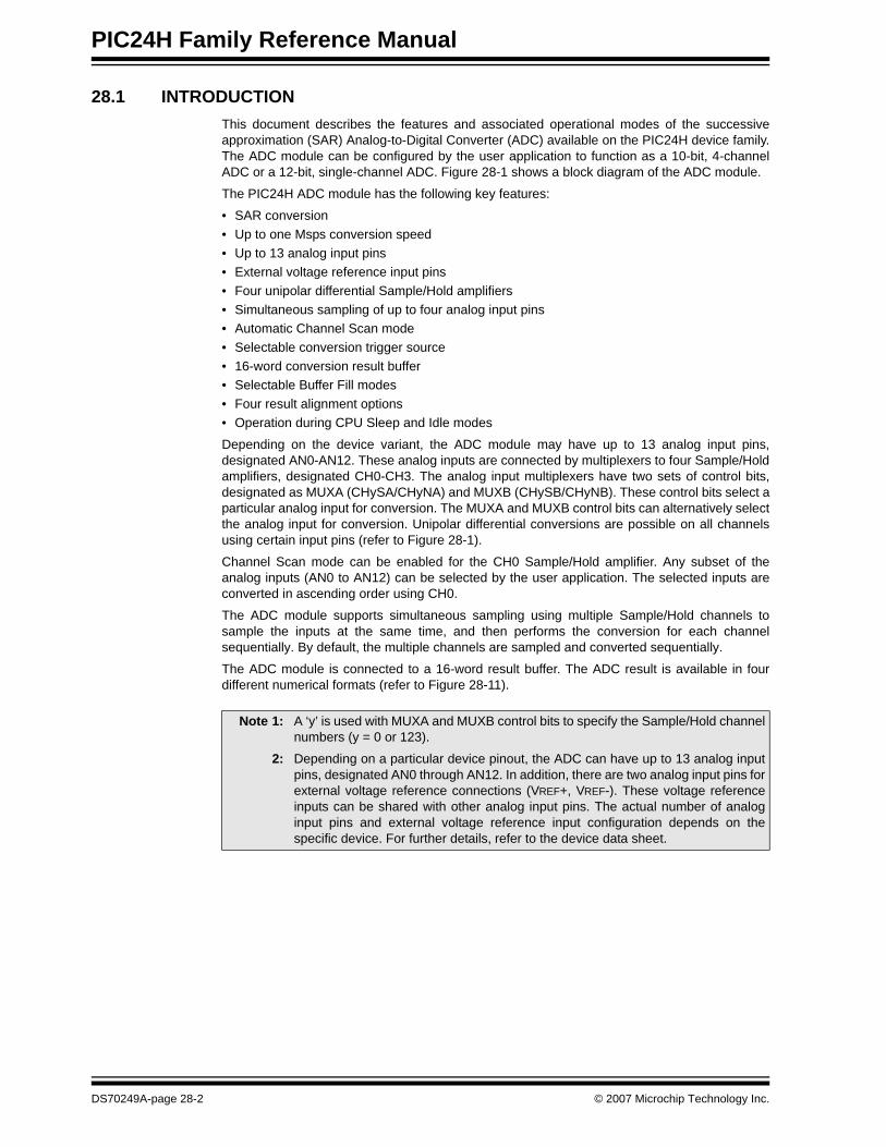
28.1 INTRODUCTIONThis document describes the features and associated operational modes of the successiveapproximation (SAR) Analog-to-Digital Converter (ADC) available on the PIC24H device family.The ADC module can be configured by the user application to function as a 10-bit, 4-channelADC or a 12-bit, single-channel ADC. Figure 28-1 shows a block diagram of the ADC module.
The PIC24H ADC module has the following key features:
• SAR conversion• Up to one Msps conversion speed• Up to 13 analog input pins• External voltage reference input pins• Four unipolar differential Sample/Hold amplifiers• Simultaneous sampling of up to four analog input pins• Automatic Channel Scan mode• Selectable conversion trigger source• 16-word conversion result buffer• Selectable Buffer Fill modes• Four result alignment options• Operation during CPU Sleep and Idle modes
Depending on the device variant, the ADC module may have up to 13 analog input pins,designated AN0-AN12. These analog inputs are connected by multiplexers to four Sample/Holdamplifiers, designated CH0-CH3. The analog input multiplexers have two sets of control bits,designated as MUXA (CHySA/CHyNA) and MUXB (CHySB/CHyNB). These control bits select aparticular analog input for conversion. The MUXA and MUXB control bits can alternatively selectthe analog input for conversion. Unipolar differential conversions are possible on all channelsusing certain input pins (refer to Figure 28-1).
Channel Scan mode can be enabled for the CH0 Sample/Hold amplifier. Any subset of theanalog inputs (AN0 to AN12) can be selected by the user application. The selected inputs areconverted in ascending order using CH0.
The ADC module supports simultaneous sampling using multiple Sample/Hold channels tosample the inputs at the same time, and then performs the conversion for each channelsequentially. By default, the multiple channels are sampled and converted sequentially.
The ADC module is connected to a 16-word result buffer. The ADC result is available in fourdifferent numerical formats (refer to Figure 28-11).
Note 1: A ‘y’ is used with MUXA and MUXB control bits to specify the Sample/Hold channelnumbers (y = 0 or 123).
2: Depending on a particular device pinout, the ADC can have up to 13 analog inputpins, designated AN0 through AN12. In addition, there are two analog input pins forexternal voltage reference connections (VREF+, VREF-). These voltage referenceinputs can be shared with other analog input pins. The actual number of analoginput pins and external voltage reference input configuration depends on thespecific device. For further details, refer to the device data sheet.
DS70249A-page 28-2 © 2007 Microchip Technology Inc.

Section 28. Analog-to-Digital Converter (ADC) without DMAA
nalog-to-Digital
Converter (A
DC
) w
ithout DM
A
28
Figure 28-1: ADC Block Diagram
SAR ADC
S/H0
S/H1
ADC1BUF0ADC1BUF1ADC1BUF2
ADC1BUFFADC1BUFE
AN0
AN12
AN1
VREF-
CH0SB<4:0>
CH0NA CH0NB
+
-
AN1
AN4
CH123SA
AN9
VREF-
CH123SB
CH123NA CH123NB
AN6
+
-
S/H2
AN2
AN5
CH123SA
AN10
VREF-
CH123SB
CH123NA CH123NB
AN7
+
-
S/H3
AN3
AN6
CH123SA
AN11
VREF-
CH123SB
CH123NA CH123NB
AN8
+
-
CH1(2)
CH0
CH2(2)
CH3(2)
CH0SA<4:0>
CHANNELSCAN
CSCNA
Alternate
VREF+(1) AVDD AVSSVREF-(1)
Note 1: VREF+, VREF- inputs can be multiplexed with other analog inputs. For details, refer to the device data sheet.2: Channels 1, 2, and 3 are not applicable for the 12-bit mode of operation.
Input Selection
VREFH VREFL
© 2007 Microchip Technology Inc. DS70249A-page 28-3

PIC24H Family Reference Manual
28.2 CONTROL REGISTERSThe ADC module has seven Control and Status registers. These registers are:
• AD1CON1: ADC1 Control Register 1• AD1CON2: ADC1 Control Register 2• AD1CON3: ADC1 Control Register 3• AD1CHS123: ADC1 Input Channel 1, 2, 3 Select Register• AD1CHS0: ADC1 Input Channel 0 Select Register• AD1CSSL: ADC1 Input Scan Select Register Low• AD1PCFGL: ADC1 Port Configuration Register LowThe AD1CON1, AD1CON2, and AD1CON3 registers control the operation of the ADC module.The AD1CHS0 and AD1CHS123 registers select the input pins to be connected to the Sample/Hold amplifiers. The AD1PCFGL register configures the analog input pins as analoginputs or as digital I/O. The AD1CSSL register selects inputs to be sequentially scanned.
28.2.1 ADC Result BufferThe ADC module contains a 16-word dual port RAM, to buffer the ADC results. The 16 bufferlocations are referred to as ADC1BUF0, ADC1BUF1, ADC1BUF2, ...., ADC1BUFE, ADC1BUFF.
DS70249A-page 28-4 © 2007 Microchip Technology Inc.

Section 28. Analog-to-Digital Converter (ADC) without DMAA
nalog-to-Digital
Converter (A
DC
) w
ithout DM
A
28
Register 28-1: AD1CON1: ADC1 Control Register 1R/W-0 U-0 R/W-0 U-0 U-0 R/W-0 R/W-0 R/W-0ADON — ADSIDL — — AD12B FORM<1:0>
bit 15 bit 8
R/W-0 R/W-0 R/W-0 U-0 R/W-0 R/W-0 R/W-0HC,HS
R/C-0HC, HS
SSRC<2:0> — SIMSAM ASAM SAMP DONEbit 7 bit 0
Legend: HC = Cleared by hardware HS = Set by hardwareR = Readable bit W = Writable bit U = Unimplemented bit, read as ‘0’-n = Value at POR ‘1’ = Bit is set ‘0’ = Bit is cleared x = Bit is unknown
bit 15 ADON: ADC Operating Mode bit1 = ADC module is operating0 = ADC module is off
bit 14 Unimplemented: Read as ‘0’bit 13 ADSIDL: Stop in Idle Mode bit
1 = Discontinue module operation when device enters Idle mode0 = Continue module operation in Idle mode
bit 12-11 Unimplemented: Read as ‘0’bit 10 AD12B: 10-bit or 12-bit Operation Mode bit
1 = 12-bit, 1-channel ADC operation0 = 10-bit, 4-channel ADC operation
bit 9-8 FORM<1:0>: Data Output Format bitsFor 10-bit operation:11 = Reserved10 = Reserved01 = Signed integer (DOUT = ssss sssd dddd dddd, where s = .NOT.d<9>)00 = Integer (DOUT = 0000 00dd dddd dddd)For 12-bit operation:11 = Signed fractional (DOUT = sddd dddd dddd 0000, where s = .NOT.d<11>)10 = Fractional (DOUT = dddd dddd dddd 0000)01 = Signed Integer (DOUT = ssss sddd dddd dddd, where s = .NOT.d<11>)00 = Integer (DOUT = 0000 dddd dddd dddd)
bit 7-5 SSRC<2:0>: Sample Clock Source Select bits111 = Internal counter ends sampling and starts conversion (auto-convert)110 = Reserved101 = Reserved100 = Reserved011 = Reserved010 = GP timer compare ends sampling and starts conversion001 = Active transition on INT0 pin ends sampling and starts conversion000 = Clearing sample bit ends sampling and starts conversion
bit 4 Unimplemented: Read as ‘0’bit 3 SIMSAM: Simultaneous Sample Select bit (only applicable when CHPS<1:0> = 01 or 1x)
When AD12B = 1, SIMSAM is: U-0, Unimplemented, Read as ‘0’1 = Samples CH0, CH1, CH2, CH3 simultaneously (when CHPS<1:0> = 1x); or
Samples CH0 and CH1 simultaneously (when CHPS<1:0> = 01)0 = Samples multiple channels individually in sequence
bit 2 ASAM: ADC Sample Auto-Start bit1 = Sampling begins immediately after last conversion. SAMP bit is auto-set0 = Sampling begins when SAMP bit is set
© 2007 Microchip Technology Inc. DS70249A-page 28-5

PIC24H Family Reference Manual
bit 1 SAMP: ADC Sample Enable bit1 = ADC Sample/Hold amplifiers are sampling0 = ADC Sample/Hold amplifiers are holdingIf ASAM = 0, software can write ‘1’ to begin sampling. Automatically set by hardware if ASAM = 1.If SSRC = 000, software can write ‘0’ to end sampling and start conversion. If SSRC ≠ 000, automatically cleared by hardware to end sampling and start conversion.
bit 0 DONE: ADC Conversion Status bit 1 = ADC conversion cycle is completed.0 = ADC conversion not started or in progressAutomatically set by hardware when analog-to-digital conversion is complete. Software can write ‘0’ to clear DONE status (software not allowed to write ‘1’). Clearing this bit does NOT affect any operation in progress. Automatically cleared by hardware at start of a new conversion.
Register 28-1: AD1CON1: ADC1 Control Register 1 (Continued)
DS70249A-page 28-6 © 2007 Microchip Technology Inc.

Section 28. Analog-to-Digital Converter (ADC) without DMAA
nalog-to-Digital
Converter (A
DC
) w
ithout DM
A
28
Register 28-2: AD1CON2: ADC1 Control Register 2R/W-0 R/W-0 R/W-0 U-0 U-0 R/W-0 R/W-0 R/W-0
VCFG<2:0> — — CSCNA CHPS<1:0>bit 15 bit 8
R-0 U-0 R/W-0 R/W-0 R/W-0 R/W-0 R/W-0 R/W-0BUFS — SMPI<3:0> BUFM ALTS
bit 7 bit 0
Legend:R = Readable bit W = Writable bit U = Unimplemented bit, read as ‘0’-n = Value at POR ‘1’ = Bit is set ‘0’ = Bit is cleared x = Bit is unknown
bit 15-13 VCFG<2:0>: Converter Voltage Reference Configuration bits
bit 12-11 Unimplemented: Read as ‘0’bit 10 CSCNA: Input Scan Select bit
1 = Scan inputs using CH0 0 = Do not scan inputs
bit 9-8 CHPS<1:0>: Channel Select bitsWhen AD12B = 1, CHPS<1:0> is: U-0, Unimplemented, Read as ‘0’ 1x = Converts CH0, CH1, CH2, and CH301 = Converts CH0 and CH100 = Converts CH0
bit 7 BUFS: Buffer Fill Status bit (only valid when BUFM = 1)1 = ADC is currently filling the second half of the buffer. The user application should access data in
the first half of the buffer0 = ADC is currently filling the first half of the buffer. The user application should access data in the
second half of the bufferbit 6 Unimplemented: Read as ‘0’bit 5-2 SMPI<3:0>: Samples Convert Sequences Per Interrupt
1111 = Interrupts at the completion of conversion for every 16th sample/convert sequence1110 = Interrupts at the completion of conversion for every 15th sample/convert sequence•
••0001 = Interrupts at the completion of conversion for every 2nd sample/convert sequence0000 = Interrupts at the completion of conversion for every sample/convert sequence
bit 1 BUFM: Buffer Fill Mode Select bit1 = Starts buffer filling the first half of the buffer on the first interrupt and the second half of the buffer
on next interrupt0 = Always starts filling the buffer from the start address
bit 0 ALTS: Alternate Input Selection Mode Select bit1 = MUXA and MUXB control bits alternatively select the analog input for conversion0 = MUXA control bits select the analog input for conversion (CSCNA = 0)
Channel Scan Logic select the analog input for conversion (CSCNA = 1)
VREFH VREFL
000 AVDD Avss001 External VREF+ Avss010 AVDD External VREF-011 External VREF+ External VREF-1xx AVDD Avss
© 2007 Microchip Technology Inc. DS70249A-page 28-7
PIC24H Family Reference Manual
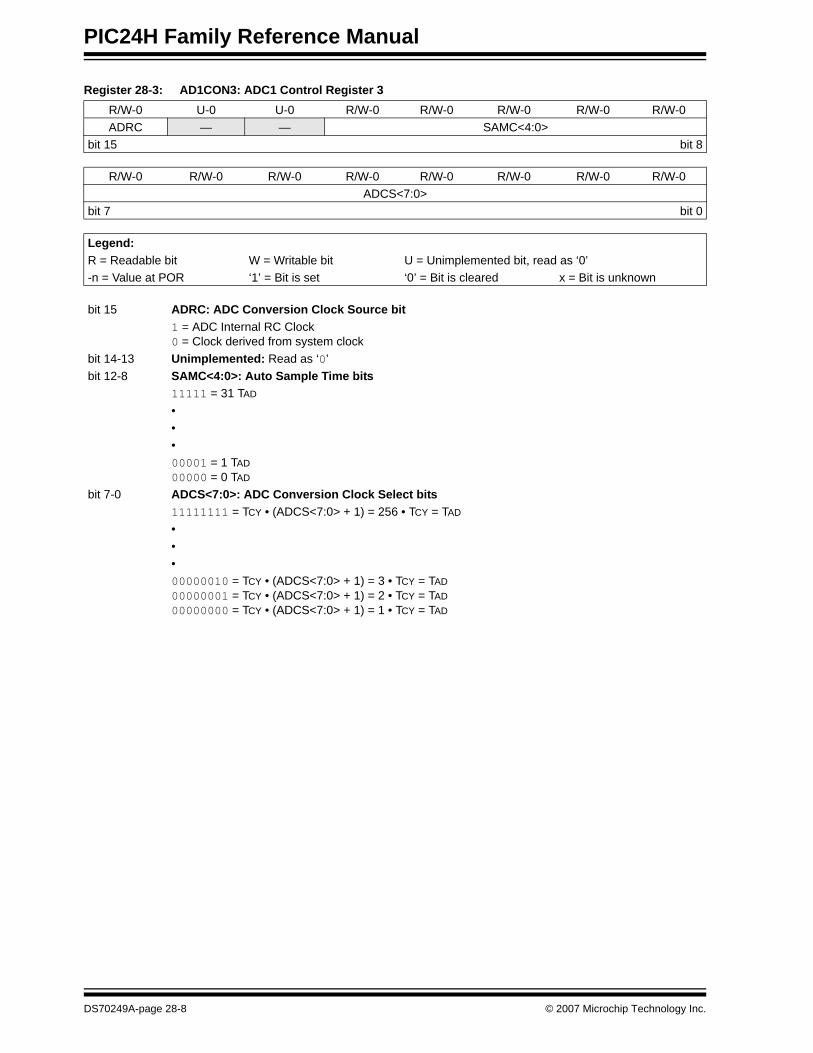
Register 28-3: AD1CON3: ADC1 Control Register 3R/W-0 U-0 U-0 R/W-0 R/W-0 R/W-0 R/W-0 R/W-0ADRC — — SAMC<4:0>
bit 15 bit 8
R/W-0 R/W-0 R/W-0 R/W-0 R/W-0 R/W-0 R/W-0 R/W-0ADCS<7:0>
bit 7 bit 0
Legend:R = Readable bit W = Writable bit U = Unimplemented bit, read as ‘0’-n = Value at POR ‘1’ = Bit is set ‘0’ = Bit is cleared x = Bit is unknown
bit 15 ADRC: ADC Conversion Clock Source bit1 = ADC Internal RC Clock0 = Clock derived from system clock
bit 14-13 Unimplemented: Read as ‘0’bit 12-8 SAMC<4:0>: Auto Sample Time bits
11111 = 31 TAD
•••00001 = 1 TAD00000 = 0 TAD
bit 7-0 ADCS<7:0>: ADC Conversion Clock Select bits11111111 = TCY • (ADCS<7:0> + 1) = 256 • TCY = TAD
•••00000010 = TCY • (ADCS<7:0> + 1) = 3 • TCY = TAD 00000001 = TCY • (ADCS<7:0> + 1) = 2 • TCY = TAD00000000 = TCY • (ADCS<7:0> + 1) = 1 • TCY = TAD
DS70249A-page 28-8 © 2007 Microchip Technology Inc.

Section 28. Analog-to-Digital Converter (ADC) without DMAA
nalog-to-Digital
Converter (A
DC
) w
ithout DM
A
28
Register 28-4: AD1CHS123: ADC1 Input Channel 1, 2, 3 Select RegisterU-0 U-0 U-0 U-0 U-0 R/W-0 R/W-0 R/W-0— — — — — CH123NB<1:0> CH123SB
bit 15 bit 8
U-0 U-0 U-0 U-0 U-0 R/W-0 R/W-0 R/W-0— — — — — CH123NA<1:0> CH123SA
bit 7 bit 0
Legend:R = Readable bit W = Writable bit U = Unimplemented bit, read as ‘0’-n = Value at POR ‘1’ = Bit is set ‘0’ = Bit is cleared x = Bit is unknown
bit 15-11 Unimplemented: Read as ‘0’bit 10-9 CH123NB<1:0>: Channel 1, 2, 3 Negative Input Select for Sample B bits
When AD12B = 1, CHxNB is: U-0, Unimplemented, Read as ‘0’11 = CH1 negative input is AN9, CH2 negative input is AN10, CH3 negative input is AN1110 = CH1 negative input is AN6, CH2 negative input is AN7, CH3 negative input is AN80x = CH1, CH2, CH3 negative input is VREF-
bit 8 CH123SB: Channel 1, 2, 3 Positive Input Select for Sample B bitWhen AD12B = 1, CHxSA is: U-0, Unimplemented, Read as ‘0’1 = CH1 positive input is AN3, CH2 positive input is AN4, CH3 positive input is AN50 = CH1 positive input is AN0, CH2 positive input is AN1, CH3 positive input is AN2
bit 7-3 Unimplemented: Read as ‘0’bit 2-1 CH123NA<1:0>: Channel 1, 2, 3 Negative Input Select for Sample A bits
When AD12B = 1, CHxNA is: U-0, Unimplemented, Read as ‘0’11 = CH1 negative input is AN9, CH2 negative input is AN10, CH3 negative input is AN1110 = CH1 negative input is AN6, CH2 negative input is AN7, CH3 negative input is AN80x = CH1, CH2, CH3 negative input is VREF-
bit 0 CH123SA: Channel 1, 2, 3 Positive Input Select for Sample A bitWhen AD12B = 1, CHxSA is: U-0, Unimplemented, Read as ‘0’1 = CH1 positive input is AN3, CH2 positive input is AN4, CH3 positive input is AN50 = CH1 positive input is AN0, CH2 positive input is AN1, CH3 positive input is AN2
© 2007 Microchip Technology Inc. DS70249A-page 28-9
PIC24H Family Reference Manual
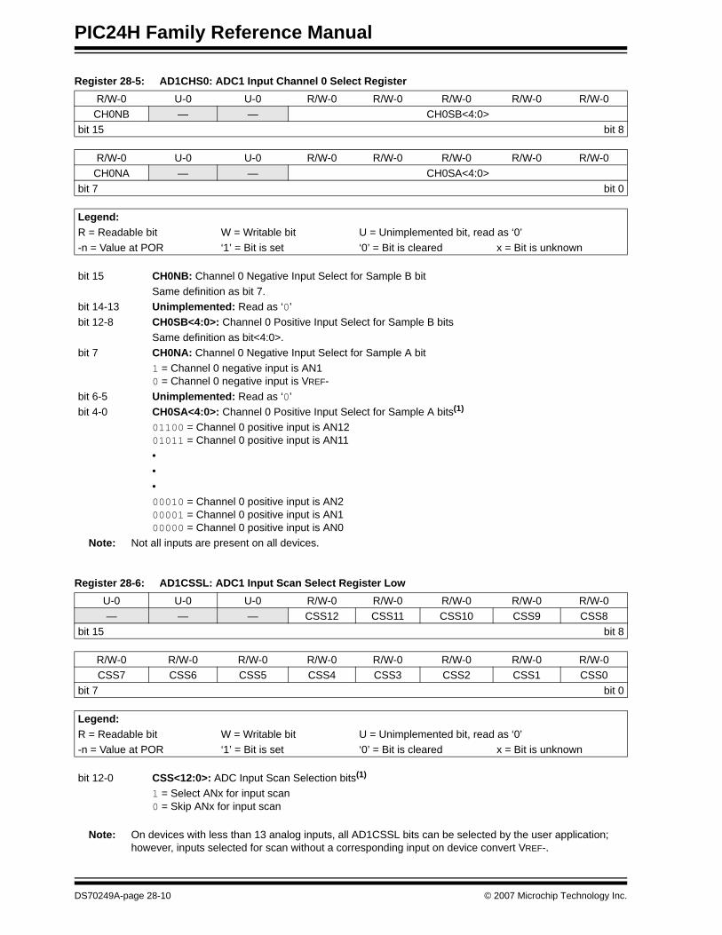
Register 28-5: AD1CHS0: ADC1 Input Channel 0 Select RegisterR/W-0 U-0 U-0 R/W-0 R/W-0 R/W-0 R/W-0 R/W-0
CH0NB — — CH0SB<4:0>bit 15 bit 8
R/W-0 U-0 U-0 R/W-0 R/W-0 R/W-0 R/W-0 R/W-0CH0NA — — CH0SA<4:0>
bit 7 bit 0
Legend:R = Readable bit W = Writable bit U = Unimplemented bit, read as ‘0’-n = Value at POR ‘1’ = Bit is set ‘0’ = Bit is cleared x = Bit is unknown
bit 15 CH0NB: Channel 0 Negative Input Select for Sample B bitSame definition as bit 7.
bit 14-13 Unimplemented: Read as ‘0’bit 12-8 CH0SB<4:0>: Channel 0 Positive Input Select for Sample B bits
Same definition as bit<4:0>.bit 7 CH0NA: Channel 0 Negative Input Select for Sample A bit
1 = Channel 0 negative input is AN10 = Channel 0 negative input is VREF-
bit 6-5 Unimplemented: Read as ‘0’bit 4-0 CH0SA<4:0>: Channel 0 Positive Input Select for Sample A bits(1)
01100 = Channel 0 positive input is AN1201011 = Channel 0 positive input is AN11•••00010 = Channel 0 positive input is AN200001 = Channel 0 positive input is AN100000 = Channel 0 positive input is AN0
Note: Not all inputs are present on all devices.
Register 28-6: AD1CSSL: ADC1 Input Scan Select Register LowU-0 U-0 U-0 R/W-0 R/W-0 R/W-0 R/W-0 R/W-0— — — CSS12 CSS11 CSS10 CSS9 CSS8
bit 15 bit 8
R/W-0 R/W-0 R/W-0 R/W-0 R/W-0 R/W-0 R/W-0 R/W-0CSS7 CSS6 CSS5 CSS4 CSS3 CSS2 CSS1 CSS0
bit 7 bit 0
Legend:R = Readable bit W = Writable bit U = Unimplemented bit, read as ‘0’-n = Value at POR ‘1’ = Bit is set ‘0’ = Bit is cleared x = Bit is unknown
bit 12-0 CSS<12:0>: ADC Input Scan Selection bits(1)
1 = Select ANx for input scan0 = Skip ANx for input scan
Note: On devices with less than 13 analog inputs, all AD1CSSL bits can be selected by the user application;however, inputs selected for scan without a corresponding input on device convert VREF-.
DS70249A-page 28-10 © 2007 Microchip Technology Inc.

Section 28. Analog-to-Digital Converter (ADC) without DMAA
nalog-to-Digital
Converter (A
DC
) w
ithout DM
A
28
Register 28-7: AD1PCFGL: ADC1 Port Configuration Register LowU-0 U-0 U-0 R/W-0 R/W-0 R/W-0 R/W-0 R/W-0— — — PCFG12 PCFG11 PCFG10 PCFG9 PCFG8
bit 15 bit 8
R/W-0 R/W-0 R/W-0 R/W-0 R/W-0 R/W-0 R/W-0 R/W-0PCFG7 PCFG6 PCFG5 PCFG4 PCFG3 PCFG2 PCFG1 PCFG0
bit 7 bit 0
Legend:R = Readable bit W = Writable bit U = Unimplemented bit, read as ‘0’-n = Value at POR ‘1’ = Bit is set ‘0’ = Bit is cleared x = Bit is unknown
bit 12-0 PCFG<12:0>: ADC Port Configuration Control bits(1, 2)
1 = Port pin in Digital mode, port read input enabled, ADC input multiplexor connected to AVSS0 = Port pin in Analog mode, port read input disabled, ADC samples pin voltage
Note 1: On devices with less than 13 analog inputs, all PCFG bits are R/W by user application; however, PCFGbits are ignored on ports without a corresponding input on device.
2: On devices with two Analog-to-Digital modules, both AD1PCFGL and AD2PCFGL affect the configurationof port pins multiplexed with AN0-AN12.
© 2007 Microchip Technology Inc. DS70249A-page 28-11
PIC24H Family Reference Manual
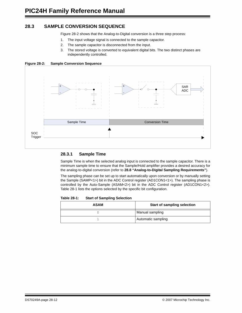
28.3 SAMPLE CONVERSION SEQUENCEFigure 28-2 shows that the Analog-to-Digital conversion is a three step process:
1. The input voltage signal is connected to the sample capacitor. 2. The sample capacitor is disconnected from the input. 3. The stored voltage is converted to equivalent digital bits. The two distinct phases are
independently controlled.
Figure 28-2: Sample Conversion Sequence
28.3.1 Sample TimeSample Time is when the selected analog input is connected to the sample capacitor. There is aminimum sample time to ensure that the Sample/Hold amplifier provides a desired accuracy forthe analog-to-digital conversion (refer to 28.8 “Analog-to-Digital Sampling Requirements”).
The sampling phase can be set up to start automatically upon conversion or by manually settingthe Sample (SAMP<1>) bit in the ADC Control register (AD1CON1<1>). The sampling phase iscontrolled by the Auto-Sample (ASAM<2>) bit in the ADC Control register (AD1CON1<2>).Table 28-1 lists the options selected by the specific bit configuration.
Table 28-1: Start of Sampling Selection
+
-
+
-
SARADC
Sample Time Conversion Time
SOC Trigger
ASAM Start of sampling selection
0 Manual sampling
1 Automatic sampling
DS70249A-page 28-12 © 2007 Microchip Technology Inc.

Section 28. Analog-to-Digital Converter (ADC) without DMAA
nalog-to-Digital
Converter (A
DC
) w
ithout DM
A
28
28.3.2 Conversion TimeThe Start of Conversion (SOC) trigger ends the sampling time and begins an analog-to-digitalconversion. During the conversion period, the sample capacitor is disconnected from themultiplexer, and the stored voltage is converted to equivalent digital bits. The conversion time for10-bit and 12-bit modes are shown in Equation 28-1 and Equation 28-2. The sum of the sampletime and the analog-to-digital conversion time provide the total conversion time.
Equation 28-1: 10-bit ADC Conversion Time
Equation 28-2: 12-bit ADC Conversion Time
The SOC trigger can be taken from a variety of hardware sources or controlled manually in usersoftware. The trigger source to initiate conversion is selected by the SOC Trigger Source Selectbits (SSRC<2:0>) in the ADC Control register (AD1CON1<7:5>). Table 28-2 lists the conversiontrigger source selection for different bit settings.
Table 28-2: SOC Trigger Selection
Table 28-3 lists the sample conversion sequence with different sample and conversion phaseselections.
Table 28-3: Sample Conversion Sequence Selection
Conversion Time = 12 • TAD
Where:TAD = ADC Clock Period
Where:TAD = ADC Clock Period
Conversion Time = 14 • TAD
SSRC<2:0> SOC Trigger Source
000 Manual Trigger
001 External Interrupt Trigger (INT0)
010 Timer Interrupt Trigger
011 Reserved
100 Reserved
101 Reserved
110 Reserved
111 Automatic Trigger
ASAM SSRC<2:0> Description
0 000 Manual Sample and Manual Conversion Sequence
0 111 Manual Sample and Automatic Conversion Sequence
0 001010011
Manual Sample and Triggered Conversion Sequence
1 000 Automatic Sample and Manual Conversion Sequence
1 111 Automatic Sample and Automatic Conversion Sequence
1 001101011
Automatic Sample and Triggered Conversion Sequence
© 2007 Microchip Technology Inc. DS70249A-page 28-13
PIC24H Family Reference Manual
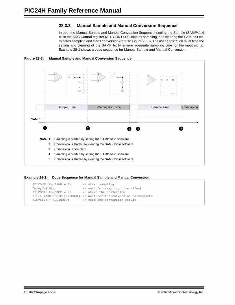
28.3.3 Manual Sample and Manual Conversion Sequence In both the Manual Sample and Manual Conversion Sequence, setting the Sample (SAMP<1>)bit in the ADC Control register (AD1CON1<1>) initiates sampling, and clearing the SAMP bit ter-minates sampling and starts conversion (refer to Figure 28-3). The user application must time thesetting and clearing of the SAMP bit to ensure adequate sampling time for the input signal.Example 28-1 shows a code sequence for Manual Sample and Manual Conversion.
Figure 28-3: Manual Sample and Manual Conversion Sequence
Example 28-1: Code Sequence for Manual Sample and Manual Conversion
+
-
+
-
Sample Time Conversion Time
SAMP
1 2
Sample Time
+
-
3 4
Conversion
5
Note 1: Sampling is started by setting the SAMP bit in software.2: Conversion is started by clearing the SAMP bit in software.3: Conversion is complete.4: Sampling is started by setting the SAMP bit in software.5: Conversion is started by clearing the SAMP bit in software.
AD1CON1bits.SAMP = 1; // start sampling DelayUs(10); // wait for sampling time (10us)AD1CON1bits.SAMP = 0; // start the conversionwhile (!AD1CON1bits.DONE); // wait for the conversion to completeADCValue = ADC1BUF0; // read the conversion result
DS70249A-page 28-14 © 2007 Microchip Technology Inc.

Section 28. Analog-to-Digital Converter (ADC) without DMAA
nalog-to-Digital
Converter (A
DC
) w
ithout DM
A
28
28.3.4 Automatic Sample and Automatic Conversion SequenceThe Auto Conversion method provides a more automated process to sample and convert theanalog inputs as shown in Figure 28-4. The sampling period is self-timed and the conversionstarts automatically upon termination of a self-timed sampling period. The Auto Sample Time(SAMC<4:0>) bits in the AD1CON3 register (AD1CON3<12:8>) select 0 to 31 ADC clock cycles(TAD) for sampling period.
Figure 28-4: Automatic Sample and Automatic Conversion Sequence
28.3.5 Automatic Sample and Triggered Conversion SequenceIn an automatic sample and triggered conversion sequence, the sampling starts automaticallyafter conversion and the conversion is started upon trigger event from the selected peripheral(refer to Figure 28-5). This allows ADC conversion to be synchronized with the internal orexternal events.
Figure 28-5: Automatic Sample and Triggered Conversion Sequence
+
-
+
-
Sample Time Conversion Time
SAMP
1 2
Sample Time
+
-
3 4
Conversion
Note 1: Sampling starts automatically after conversion.2: Conversion starts automatically upon termination of self timed sampling period.3: Sampling starts automatically after conversion.4: Conversion starts automatically upon termination of self timed sampling period.
N • TAD N • TAD
Conversion
+
-
+
-
Sample Time Conversion Time
SAMP
1 2
Sample Time
+
-
3 4
Conversion
Note 1: Sampling starts automatically after conversion.2: Conversion starts upon trigger event.3: Sampling starts automatically after conversion.4: Conversion starts upon trigger event.
Conversion
SOC Trigger
© 2007 Microchip Technology Inc. DS70249A-page 28-15

PIC24H Family Reference Manual
28.3.6 Multi-Channel Sample Conversion SequenceMulti-channel analog-to-digital converters typically convert each input channel sequentially usingan input multiplexer. Certain applications require simultaneous sampling, especially when phaseinformation exists between different channels. For example, motor control and power monitoringrequires voltage and current measurements and the phase angle between them. Figure 28-6 andFigure 28-7 show the ADC module supports simultaneous sampling using two Sample/Hold orfour Sample/Hold channels to sample the inputs at the same instant and then perform the conversion for each channel sequentially.
The Simultaneous Sampling mode is selected by setting Simultaneous Sampling (SIMSAM<3>)bit in the ADC Control register (AD1CON1<3>). By default, the multiple channels are sampledand converted sequentially. Table 28-4 lists the options selected by a specific bit configuration.
Table 28-4: Start of Sampling Selection
Figure 28-6: 2-Channel Simultaneous Sampling (ASAM = 1)
SIMSAM Sampling Mode
0 Sequential sampling
1 Simultaneous sampling
Sample 1
Sample 1
CH0
CH1
Convert 1
Convert 1
SOC Trigger
Sample 2
Sample 2
Convert 2
Convert 2
Sample/Convert Sequence 1 Sample/Convert Sequence 2
1 2 43 5
Note 1: CH0-CH1 Input multiplexer selects analog input for sampling. The selected analog input is connectedto the sample capacitor.
2: On SOC Trigger, CH0-CH1 sample capacitor is disconnected from the multiplexer to simultaneouslysample the analog inputs. The analog value captured in CH0 is converted to equivalent digital counts.
3: The analog voltage captured in CH1 is converted to equivalent digital counts.4: CH0-CH1 Input multiplexer selects next analog input for sampling. The selected analog input is
connected to the sample capacitor.5: On SOC Trigger, CH0-CH1 sample capacitor is disconnected from the multiplexer to simultaneously
sample the analog inputs. The analog value captured in CH0 is converted to equivalent digital counts.
DS70249A-page 28-16 © 2007 Microchip Technology Inc.
Section 28. Analog-to-Digital Converter (ADC) without DMAA
nalog-to-Digital
Converter (A
DC
) w
ithout DM
A
28
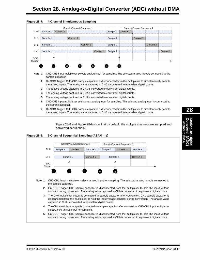
Figure 28-7: 4-Channel Simultaneous Sampling
Figure 28-8 and Figure 28-9 show that by default, the multiple channels are sampled and converted sequentially.
Figure 28-8: 2-Channel Sequential Sampling (ASAM = 1)
Sample 1
Sample 1
CH0
CH1
Sample 1
Sample 1
CH2
CH3
Convert 1
Convert 1
Convert 1
Convert
SOC Trigger
Convert 1
Sample 2
Sample 2
Sample 2
Sample 2
Convert 2
Convert 2
Convert 2
Convert2
Sample/Convert Sequence 1 Sample/Convert Sequence 2
1 2 4 73 5 6
Note 1: CH0-CH3 Input multiplexer selects analog input for sampling. The selected analog input is connected to thesample capacitor.
2: On SOC Trigger, CH0-CH3 sample capacitor is disconnected from the multiplexer to simultaneously samplethe analog inputs. The analog value captured in CH0 is converted to equivalent digital counts.
3: The analog voltage captured in CH1 is converted to equivalent digital counts.4: The analog voltage captured in CH2 is converted to equivalent digital counts.5: The analog voltage captured in CH3 is converted to equivalent digital counts.6: CH0-CH3 Input multiplexer selects next analog input for sampling. The selected analog input is connected to
the sample capacitor.7: On SOC Trigger, CH0-CH4 sample capacitor is disconnected from the multiplexer to simultaneously sample
the analog inputs. The analog value captured in CH0 is converted to equivalent digital counts.
Sample 1
Sample 1
CH0
CH1
Convert 1
Convert 1
SOC Trigger
Sample 2
Sample 2
Convert 2
Convert 2
Sample/Convert Sequence 1 Sample/Convert Sequence 2
Sample 2 Sample 3
1 2 43 5
Note 1: CH0-CH1 Input multiplexer selects analog input for sampling. The selected analog input is connected tothe sample capacitor.
2: On SOC Trigger, CH0 sample capacitor is disconnected from the multiplexer to hold the input voltageconstant during conversion. The analog value captured in CH0 is converted to equivalent digital counts.
3: The CH0 multiplexer output is connected to sample capacitor after conversion. CH1 sample capacitor isdisconnected from the multiplexer to hold the input voltage constant during conversion. The analog valuecaptured in CH1 is converted to equivalent digital counts.
4: The CH1 multiplexer output is connected to sample capacitor after conversion. CH0-CH1 Input multiplexerselects next analog input for sampling.
5: On SOC Trigger, CH0 sample capacitor is disconnected from the multiplexer to hold the input voltageconstant during conversion. The analog value captured in CH0 is converted to equivalent digital counts.
© 2007 Microchip Technology Inc. DS70249A-page 28-17
PIC24H Family Reference Manual
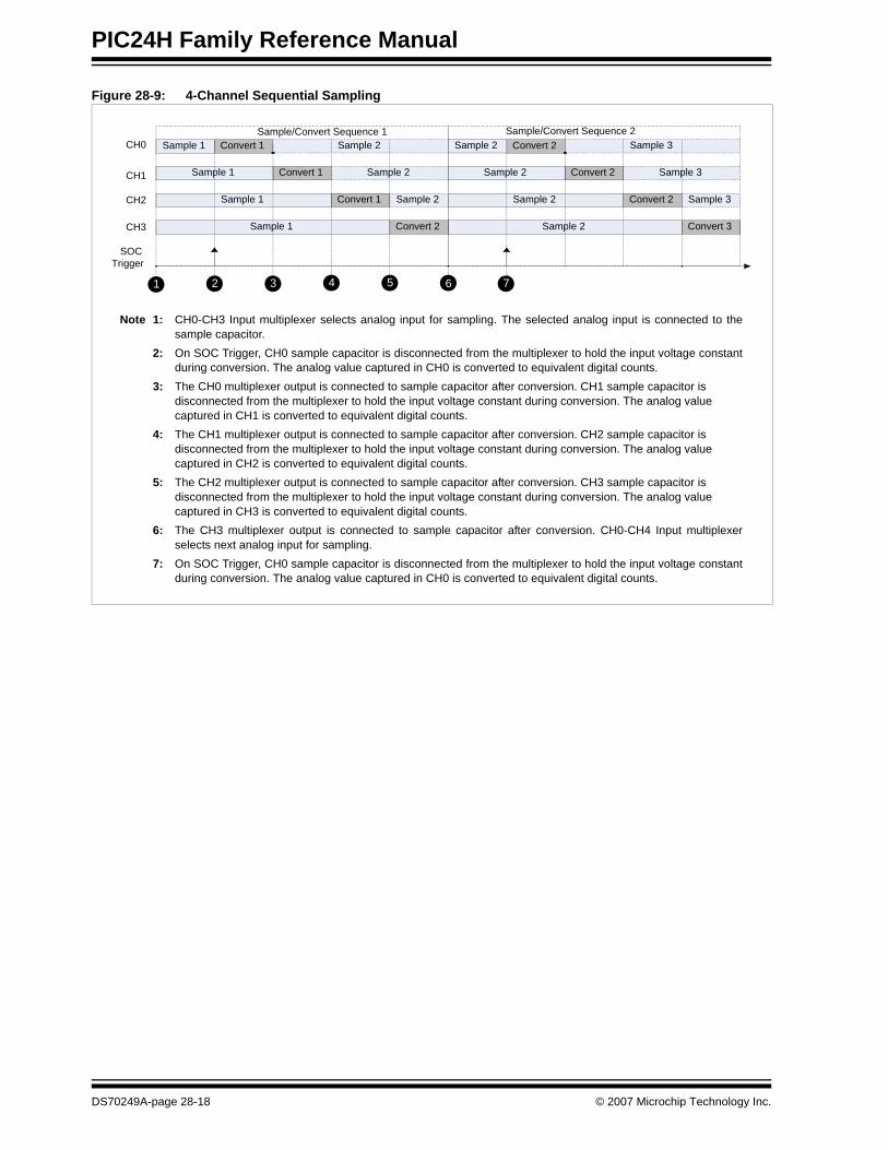
Figure 28-9: 4-Channel Sequential Sampling
Sample 1CH0
CH1
CH2
CH3
Convert 1
Convert 1
Convert 2
Convert 1
SOC Trigger
Sample 1
Sample 1
Sample 1
Convert 2
Convert 2
Convert 3
Convert 2Sample 2
Sample 2
Sample 2
Sample 2Sample/Convert Sequence 1 Sample/Convert Sequence 2
Sample 2
Sample 2
Sample 2
Sample 3
Sample 3
Sample 3
1 2 4 73 5 6
Note 1: CH0-CH3 Input multiplexer selects analog input for sampling. The selected analog input is connected to thesample capacitor.
2: On SOC Trigger, CH0 sample capacitor is disconnected from the multiplexer to hold the input voltage constantduring conversion. The analog value captured in CH0 is converted to equivalent digital counts.
3: The CH0 multiplexer output is connected to sample capacitor after conversion. CH1 sample capacitor is disconnected from the multiplexer to hold the input voltage constant during conversion. The analog value captured in CH1 is converted to equivalent digital counts.
4: The CH1 multiplexer output is connected to sample capacitor after conversion. CH2 sample capacitor is disconnected from the multiplexer to hold the input voltage constant during conversion. The analog value captured in CH2 is converted to equivalent digital counts.
5: The CH2 multiplexer output is connected to sample capacitor after conversion. CH3 sample capacitor is disconnected from the multiplexer to hold the input voltage constant during conversion. The analog value captured in CH3 is converted to equivalent digital counts.
6: The CH3 multiplexer output is connected to sample capacitor after conversion. CH0-CH4 Input multiplexerselects next analog input for sampling.
7: On SOC Trigger, CH0 sample capacitor is disconnected from the multiplexer to hold the input voltage constantduring conversion. The analog value captured in CH0 is converted to equivalent digital counts.
DS70249A-page 28-18 © 2007 Microchip Technology Inc.
Section 28. Analog-to-Digital Converter (ADC) without DMAA
nalog-to-Digital
Converter (A
DC
) w
ithout DM
A
28
28.4 ADC CONFIGURATION
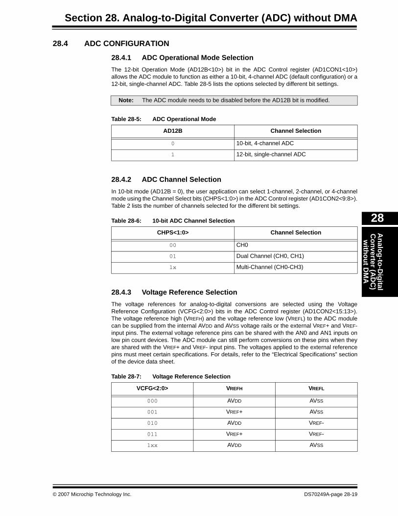
28.4.1 ADC Operational Mode SelectionThe 12-bit Operation Mode (AD12B<10>) bit in the ADC Control register (AD1CON1<10>)allows the ADC module to function as either a 10-bit, 4-channel ADC (default configuration) or a12-bit, single-channel ADC. Table 28-5 lists the options selected by different bit settings.
Table 28-5: ADC Operational Mode
28.4.2 ADC Channel SelectionIn 10-bit mode (AD12B = 0), the user application can select 1-channel, 2-channel, or 4-channelmode using the Channel Select bits (CHPS<1:0>) in the ADC Control register (AD1CON2<9:8>).Table 2 lists the number of channels selected for the different bit settings.
Table 28-6: 10-bit ADC Channel Selection
28.4.3 Voltage Reference SelectionThe voltage references for analog-to-digital conversions are selected using the VoltageReference Configuration (VCFG<2:0>) bits in the ADC Control register (AD1CON2<15:13>).The voltage reference high (VREFH) and the voltage reference low (VREFL) to the ADC modulecan be supplied from the internal AVDD and AVSS voltage rails or the external VREF+ and VREF-input pins. The external voltage reference pins can be shared with the AN0 and AN1 inputs onlow pin count devices. The ADC module can still perform conversions on these pins when theyare shared with the VREF+ and VREF- input pins. The voltages applied to the external referencepins must meet certain specifications. For details, refer to the “Electrical Specifications” sectionof the device data sheet.
Table 28-7: Voltage Reference Selection
Note: The ADC module needs to be disabled before the AD12B bit is modified.
AD12B Channel Selection
0 10-bit, 4-channel ADC
1 12-bit, single-channel ADC
CHPS<1:0> Channel Selection
00 CH0
01 Dual Channel (CH0, CH1)
1x Multi-Channel (CH0-CH3)
VCFG<2:0> VREFH VREFL
000 AVDD AVSS
001 VREF+ AVSS
010 AVDD VREF-
011 VREF+ VREF-
1xx AVDD AVSS
© 2007 Microchip Technology Inc. DS70249A-page 28-19

PIC24H Family Reference Manual
28.4.4 ADC Clock SelectionThe ADC module can be clocked from the instruction cycle clock (TCY) or by using the dedicatedinternal RC clock (see Figure 7). When using the instruction cycle clock, a clock divider drivesthe instruction cycle clock and allows a lower frequency to be chosen. The clock divider is controlled by the ADC Conversion Clock Select (ADCS<7:0>) bits in the ADC Control register(AD1CON3<5:0>), which allows 256 settings, from 1:1 to 1:256, to be chosen.
Equation 28-3 shows the ADC Clock period (TAD) as a function of the ADCS control bits and thedevice instruction cycle clock period, TCY.
Equation 28-3: ADC Clock Period
The ADC module has a dedicated internal RC clock source that can be used to performconversions. The internal RC clock source is used when analog-to-digital conversions are performed while the device is in Sleep mode. The internal RC oscillator is selected by setting theADC Conversion Clock Source (ADRC<15>) bit in the ADC Control register (AD1CON3<15>).When the ADRC bit is set, the ADCS<7:0> bits have no effect on the ADC operation.
Figure 28-10: ADC Clock Generation
28.4.5 Output Data Format SelectionFigure 28-11 shows the ADC result is available in four different numerical formats. The Data Output Format (FORM<1:0>) bits in the ADC Control register (AD1CON1<9:8>) select the outputdata format. Table 28-8 lists the ADC output format for different bit settings.
Table 28-8: ADC Output Format Selection
FORM<1:0> Data Information Selection
01 Signed Integer format
00 Unsigned Integer format
ADC Clock Period (TAD) = TCY • (ADCS + 1)
0
1ADCS<7:0>
ADRC
ADC Clock (TAD)
TCY
ADC Internal RC
N
DS70249A-page 28-20 © 2007 Microchip Technology Inc.

Section 28. Analog-to-Digital Converter (ADC) without DMAA
nalog-to-Digital
Converter (A
DC
) w
ithout DM
A
28
Figure 28-11: ADC Output Format
0000 0000 0000 0000 (0)
0000 0011 1111 1111 (1023)
0000 0010 0000 0000 (512)
1111 1110 0000 0000 (-512)
0000 0001 1111 1111 (511)
0000 0000 0000 0000 (0)
0000 0000 0000 0000 (0)
0000 1111 1111 1111 (4095)
0000 1000 0000 0000 (2048)
1111 1000 0000 0010 (-2046)
0000 0111 1111 1101 (2045)
0000 0000 0000 0000 (0)
FORM = 0b00Unsigned Integer
FORM = 0b01Signed Integer
VREFHVREFL Input
VREFHVREFL Input
VREFHVREFL Input
VREFHVREFL Input
10-Bit ADC 10-Bit ADC
© 2007 Microchip Technology Inc. DS70249A-page 28-21
PIC24H Family Reference Manual
28.4.6 Configuring Analog Port PinsThe Analog/Digital Pin Configuration register (AD1PCFGL) specifies the input condition of devicepins used as analog inputs. Along with the Data Direction (TRISx) register in the Parallel I/O Portmodule, these registers control the operation of the ADC pins.
A pin is configured as an analog input when the corresponding PCFGn bit (AD1PCFGL<n>) isclear. The AD1PCFGL register is cleared at Reset, causing the ADC input pins to be configuredfor analog input by default at Reset.
When configured for analog input, the associated port I/O digital input buffer is disabled so thatit does not consume current.
The port pins that are desired as analog inputs must have their corresponding TRIS bit set,specifying the port input. If the I/O pin associated with an analog-to-digital input is configured asan output, the TRIS bit is cleared and the digital output level (VOH or VOL) of the port is converted.After a device Reset, all TRIS bits are set.
A pin is configured as a digital I/O when the corresponding PCFGn bit is set. In this configuration,the input to the analog multiplexer is connected to AVSS.
28.4.7 Enabling the ADC ModuleWhen the ADON bit (AD1CON1<15>) is ‘1’, the module is in Active mode and is fully poweredand functional.
When ADON is ‘0’, the module is disabled. The digital and analog portions of the circuit areturned off for maximum current savings.
To return to the Active mode from the Off mode, the user application must wait for the analogstages to stabilize. For the stabilization time, refer to the “Electrical Characteristics” section of thedevice data sheet.
Note 1: When the ADC Port register is read, any pin configured as an analog input readsas a '0'.
2: Analog levels on any pin that is defined as a digital input may cause the input bufferto consume current that is out of the device specification.
Note: The SSRC<2:0>, SIMSAM, ASAM, CHPS<1:0>, SMPI<3:0>, BUFM, and ALTSbits, as well as the ADCON3 and ADCSSL registers, should not be written to whileADON = 1. This would lead to indeterminate results.
DS70249A-page 28-22 © 2007 Microchip Technology Inc.
Section 28. Analog-to-Digital Converter (ADC) without DMAA
nalog-to-Digital
Converter (A
DC
) w
ithout DM
A
28
28.5 ADC INTERRUPT GENERATIONAs conversions are completed, the ADC module writes the results of the conversions into theanalog-to-digital result buffer. The ADC result buffer is an array of sixteen words, accessedthrough the SFR space. The user application may attempt to read each analog-to-digitalconversion result as it is generated. However, this might consume too much CPU time.Generally, to simplify the code, the module fills the buffer with results and generates an interruptwhen the buffer is filled. The ADC module supports 16 result buffers. Therefore, the maximumnumber of conversions per interrupt must not exceed 16.The number of conversion per ADC interrupt depends on the following parameters, which canvary from one to 16 conversions per interrupt.
• Number of Sample/Hold channels selected• Sequential or Simultaneous Sampling • Samples Convert Sequences Per Interrupt (SMPI<3:0>) bit settings
Table 28-9 lists the number of conversions per ADC interrupt for different configuration modes.
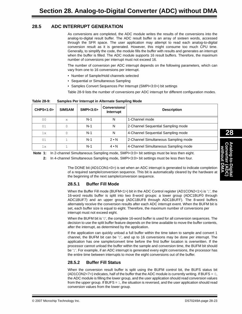
Table 28-9: Samples Per Interrupt in Alternate Sampling Mode
The DONE bit (AD1CON1<0>) is set when an ADC interrupt is generated to indicate completionof a required sample/conversion sequence. This bit is automatically cleared by the hardware atthe beginning of the next sample/conversion sequence.
28.5.1 Buffer Fill ModeWhen the Buffer Fill mode (BUFM<1>) bit in the ADC Control register (AD1CON2<1>) is '1', the16-word results buffer is split into two 8-word groups: a lower group (ADC1BUF0 throughADC1BUF7) and an upper group (ADC1BUF8 through ADC1BUFF). The 8-word buffersalternately receive the conversion results after each ADC interrupt event. When the BUFM bit isset, each buffer size is equal to eight. Therefore, the maximum number of conversions per interrupt must not exceed eight.When the BUFM bit is '0', the complete 16-word buffer is used for all conversion sequences. Thedecision to use the split buffer feature depends on the time available to move the buffer contents,after the interrupt, as determined by the application. If the application can quickly unload a full buffer within the time taken to sample and convert 1channel, the BUFM bit can be '0', and up to 16 conversions may be done per interrupt. Theapplication has one sample/convert time before the first buffer location is overwritten. If theprocessor cannot unload the buffer within the sample and conversion time, the BUFM bit shouldbe '1'. For example, if an ADC interrupt is generated every eight conversions, the processor hasthe entire time between interrupts to move the eight conversions out of the buffer.
28.5.2 Buffer Fill StatusWhen the conversion result buffer is split using the BUFM control bit, the BUFS status bit(AD1CON2<7>) indicates, half of the buffer that the ADC module is currently writing. If BUFS = 0,the ADC module is filling the lower group, and the user application should read conversion valuesfrom the upper group. If BUFS = 1, the situation is reversed, and the user application should readconversion values from the lower group.
CHPS<1:0> SIMSAM SMPI<3:0> Conversions/Interrupt Description
00 x N-1 N 1-Channel mode
01 0 N-1 N 2-Channel Sequential Sampling mode
1x 0 N-1 N 4-Channel Sequential Sampling mode
01 1 N-1 2 • N 2-Channel Simultaneous Sampling mode
1x 1 N-1 4 • N 4-Channel Simultaneous Sampling mode
Note 1: In 2-channel Simultaneous Sampling mode, SMPI<3:0> bit settings must be less then eight.2: In 4-channel Simultaneous Sampling mode, SMPI<3:0> bit settings must be less then four.
© 2007 Microchip Technology Inc. DS70249A-page 28-23

PIC24H Family Reference Manual
28.6 ANALOG INPUT SELECTION FOR CONVERSIONThe ADC module provides a flexible mechanism to select analog inputs for conversion:
• Fixed input selection• Alternate input selection• Channel scanning (CH0 only)
28.6.1 Fixed Input SelectionThe 10-bit ADC configuration can use up to four Sample/Hold channels, designated CH0-CH3,whereas the 12-bit ADC configuration can use only one Sample/Hold channel, CH0. TheSample/Hold channels are connected to the analog input pins through the analog multiplexer.The analog input multiplexer is controlled by the AD1CHS123 and AD1CHS0 registers. Thereare two sets of control bits designated as MUXA (CHySA/CHyNA) and MUXB (CHySB/CHyNB)to select a particular input source for conversion. The MUXB control bits are used in AlternateInput Selection mode. By default, the MUXA bits select the analog input for conversion.
Table 28-10: Analog Input Selection
Example 28-2 shows the code sequence to set up ADC inputs for a 4-channel ADCconfiguration.
Example 28-2: Code Sequence to Set Up ADC Inputs
MUXA MUXBControl bits Analog Inputs Control bits Analog Inputs
CH0 +ve CH0SA<4:0> AN0 to AN12 CH0SB<4:0> AN0 to AN12
-ve CH0NA VREF-, AN1 CH0NB AN0 to AN12
CH1 +ve CH123SA AN0, AN3 CH123SB AN0, AN3
-ve CH123NA<1:0> AN6, AN9, VREF- CH123NB<1:0> AN6, AN9, VREF-
CH2 +ve CH123SA AN1, AN4 CH123SB AN1, AN4
-ve CH123NA<1:0> AN7, AN10, VREF- CH123NB<1:0> AN7, AN10, VREF-
CH3 +ve CH123SA AN2, AN5 CH123SB AN2, AN5
-ve CH123NA<1:0> AN8, AN11, VREF- CH123NB<1:0> AN8, AN11, VREF-
Note: Not all inputs are present on all devices.
// Initialize MUXA Input SelectionAD1CHS0bits.CH0SA = 3; // Select AN3 for CH0 +ve inputAD1CHS0bits.CH0NA = 0; // Select VREF- for CH0 -ve input
AD1CHS123bits.CH123SA=0; // Select AN0 for CH1 +ve input// Select AN1 for CH2+ve input// Select AN2 for CH3 +ve input
AD1CHS123bits.CH124NA=0; // Select VREF- for CH1/CH2/CH3 -ve inputs
DS70249A-page 28-24 © 2007 Microchip Technology Inc.

Section 28. Analog-to-Digital Converter (ADC) without DMAA
nalog-to-Digital
Converter (A
DC
) w
ithout DM
A
28
28.6.2 Alternate Input Selection modeIn an Alternate Input Selection mode, the MUXA and MUXB control bits select the channel forconversion. The ADC completes one sweep using the MUXA selection, and then another sweepusing the MUXB selection, and then another sweep using the MUXA selection, and so on. TheAlternate Input Selection mode is enabled by setting the Alternate Sample (ALTS<0>) bit in theADC control register (AD1CON2<0>).
For Alternate Input Selection mode, an ADC interrupt must be generated after an even numberof sample/conversion sequences by programming the Samples Convert Sequences PerInterrupt (SMPI<3:0>)bits. Table 28-11 shows the valid SMPI values for Alternate Input Selectionmode in different ADC configurations.
Table 28-11: Valid SMPI Values for Alternate Input Selection Mode
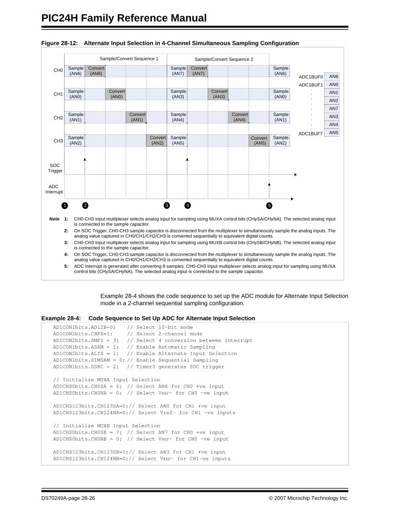
Example 28-3 shows the code sequence to set up the ADC module for Alternate Input Selectionmode in the 4-Channel Simultaneous Sampling configuration. Figure 28-12 shows the ADCmodule operation sequence.
Example 28-3: Code Sequence to Set Up ADC for Alternate Input Selection Mode
CHPS<1:0> SIMSAM SMPI<3:0>(Decimal)
Conversions/Interrupt Description
00 x 1,3,5,7,9,11,13,15 2,4,6,8,10,12,14,16 1- Channel mode
01 0 3,7,11,15 4,8,12,16 2- Channel Sequential Sampling mode
1x 0 7,15 8,16 4- Channel Sequential Sampling mode
01 1 1,3,5,7 4,8,12,16 2- Channel Simultaneous Sampling mode
1x 1 1,3 8,16 4- Channel Simultaneous Sampling mode
Note: On ADC Interrupt, the ADC internal logic is initialized to restart the conversionsequence from the beginning.
AD1CON1bits.AD12B = 0; // Select 10-bit modeAD1CON2bits.CHPS = 3; // Select 4-channel modeAD1CON1bits.SIMSAM = 1; // Enable Simultaneous SamplingAD1CON2bits.ALTS = 1; // Enable Alternate Input SelectionAD1CON2bits.SMPI = 1; // Select 8 conversion between interruptAD1CON1bits.ASAM = 1; // Enable Automatic Sampling AD1CON1bits.SSRC = 2; // Timer3 generates SOC trigger
// Initialize MUXA Input SelectionAD1CHS0bits.CH0SA = 6; // Select AN6 for CH0 +ve inputAD1CHS0bits.CH0NA = 0; // Select VREF- for CH0 -ve inputAD1CHS123bits.CH123SA = 0; // Select CH1 +ve = AN0, CH2 +ve = AN1, CH3 +ve = AN2AD1CHS123bits.CH124NA = 0; // Select VREF- for CH1/CH2/CH3 -ve inputs
// Initialize MUXB Input SelectionAD1CHS0bits.CH0SB = 7; // Select AN7 for CH0 +ve inputAD1CHS0bits.CH0NB = 0; // Select VREF- for CH0 -ve input
AD1CHS123bits.CH123SB = 1; // Select CH1 +ve = AN3, CH2 +ve = AN4, CH3 +ve = AN5
© 2007 Microchip Technology Inc. DS70249A-page 28-25
PIC24H Family Reference Manual
Figure 28-12: Alternate Input Selection in 4-Channel Simultaneous Sampling Configuration
Example 28-4 shows the code sequence to set up the ADC module for Alternate Input Selectionmode in a 2-channel sequential sampling configuration.
Example 28-4: Code Sequence to Set Up ADC for Alternate Input Selection
Sample(AN6)
Sample(AN0)
CH0
CH1
Sample(AN1)
Sample(AN2)
CH2
CH3
Convert(AN6)
Convert(AN0)
Convert(AN1)
Convert
SOC Trigger
Convert(AN2)
Sample(AN7)
Sample(AN3)
Sample(AN4)
Sample(AN5)
Convert(AN7)
Convert(AN3)
Convert(AN4)
Convert(AN5)
Sample/Convert Sequence 1 Sample/Convert Sequence 2
Sample(AN6)
Sample(AN0)
Sample(AN1)
Sample(AN2)
2 3 5
ADC Interrupt
1 4
AN6
AN0
AN1
AN2
AN7
AN3
AN4
AN5
ADC1BUF0
ADC1BUF1
ADC1BUF7
Note 1: CH0-CH3 Input multiplexer selects analog input for sampling using MUXA control bits (CHySA/CHyNA). The selected analog inputis connected to the sample capacitor.
2: On SOC Trigger, CH0-CH3 sample capacitor is disconnected from the multiplexer to simultaneously sample the analog inputs. Theanalog value captured in CH0/CH1/CH2/CH3 is converted sequentially to equivalent digital counts.
3: CH0-CH3 Input multiplexer selects analog input for sampling using MUXB control bits (CHySB/CHyNB). The selected analog inputis connected to the sample capacitor.
4: On SOC Trigger, CH0-CH3 sample capacitor is disconnected from the multiplexer to simultaneously sample the analog inputs. Theanalog value captured in CH0/CH1/CH2/CH3 is converted sequentially to equivalent digital counts.
5: ADC Interrupt is generated after converting 8 samples. CH0-CH3 Input multiplexer selects analog input for sampling using MUXAcontrol bits (CHySA/CHyNA). The selected analog input is connected to the sample capacitor.
AD1CON1bits.AD12B=0; // Select 10-bit modeAD1CON2bits.CHPS=1; // Select 2-channel modeAD1CON2bits.SMPI = 3; // Select 4 conversion between interruptAD1CON1bits.ASAM = 1; // Enable Automatic Sampling AD1CON2bits.ALTS = 1; // Enable Alternate Input SelectionAD1CON1bits.SIMSAM = 0; // Enable Sequential SamplingAD1CON1bits.SSRC = 2; // Timer3 generates SOC trigger
// Initialize MUXA Input SelectionAD1CHS0bits.CH0SA = 6; // Select AN6 for CH0 +ve inputAD1CHS0bits.CH0NA = 0; // Select VREF- for CH0 -ve input
AD1CHS123bits.CH123SA=0;// Select AN0 for CH1 +ve inputAD1CHS123bits.CH124NA=0;// Select Vref- for CH1 -ve inputs
// Initialize MUXB Input SelectionAD1CHS0bits.CH0SB = 7; // Select AN7 for CH0 +ve inputAD1CHS0bits.CH0NB = 0; // Select VREF- for CH0 -ve input
AD1CHS123bits.CH123SB=1;// Select AN3 for CH1 +ve inputAD1CHS123bits.CH124NB=0;// Select VREF- for CH1-ve inputs
DS70249A-page 28-26 © 2007 Microchip Technology Inc.

Section 28. Analog-to-Digital Converter (ADC) without DMAA
nalog-to-Digital
Converter (A
DC
) w
ithout DM
A
28
Figure 28-13: Alternate Input Selection in 2-Channel Sequential Sampling Configuration
28.6.3 Channel ScanningThe ADC module supports the Channel Scan mode using CH0 (Sample/Hold channel '0'). Thenumber of inputs scanned is software selectable. Any subset of the analog inputs from AN0 toAN12 can be selected for conversion. The selected inputs are converted in ascending order. Forexample, if the input selection includes AN4, AN1, and AN3, the conversion sequence is AN1,AN3, and AN4. The conversion sequence selection is made by programming the Channel Selectregister (AD1CSSL). A logic ‘1’ in the Channel Select register marks the associated analog inputchannel for inclusion in the conversion sequence. The Channel Scanning mode is enabled bysetting the Channel Scan (CSCNA<10>) bit in the ADC Control register (AD1CON2<10>). InChannel Scan mode, MUXA software control is ignored and the ADC module sequences throughthe enabled channels.
For every sample/convert sequence, one analog input is scanned. The ADC interrupt must begenerated after all selected channels are scanned. If “N” inputs are enabled for channel scan, aninterrupt must be generated after “N” sample/convert sequence. Table 28-12 shows the SMPIvalues to scan “N” analog inputs using CH0 in different ADC configurations.
Table 28-12: Conversions per interrupt in Channel Scan Mode
Sample(AN6)
Sample (AN0)
CH0
CH1
Convert(AN6)
Convert(AN0)
SOC Trigger
Sample(AN7)
Sample(AN3)
Convert (AN7)
Convert(AN3)
Sample/Convert Sequence 1 Sample/Convert Sequence 2
Sample(AN7)
Sample(AN6)
1 2 3 4 5
ADC Interrupt
Sample(AN6)
Sample(AN0)
AN6
AN0
AN7
AN3
ADC1BUF0
ADC1BUF1
ADC1BUF2
ADC1BUF3
Note 1: CH0-CH1 Input multiplexer selects analog input for sampling using MUXA control bits (CHySA/CHyNA). The selected analoginput is connected to the sample capacitor.
2: On SOC Trigger, CH0/CH1 inputs are sequentially sampled and converted to equivalent digital counts. 3: CH0-CH1 Input multiplexer selects analog input for sampling using MUXB control bits (CHySB/CHyNB). The selected analog
input is connected to the sample capacitor. 4: On SOC Trigger, CH0/CH1 inputs are sequentially sampled and converted to equivalent digital counts. 5: ADC Interrupt is generated after converting 4 samples. CH0-CH1 Input multiplexer selects analog input for sampling using
MUXA control bits (CHySA/CHyNA). The selected analog input is connected to the sample capacitor.
CHPS<1:0> SIMSAM SMPI<3:0>(Decimal)
Conversions/Interrupt
Description
00 x N-1 N 1-Channel mode
01 0 2N-1 2N 2-Channel Sequential Sampling mode
1x 0 4N-1 4N 4-Channel Sequential Sampling mode
01 1 N-1 2N 2-Channel Simultaneous Sampling mode
1x 1 N-1 4N 4-Channel Simultaneous Sampling mode
© 2007 Microchip Technology Inc. DS70249A-page 28-27

PIC24H Family Reference Manual
Example 28-5 shows the code sequence to scan four analog inputs using CH0. Figure 28-14shows the ADC operation sequence.
Example 28-5: Code sequence to Scan four Analog Inputs Using CH0
Figure 28-14: Scan Four Analog Inputs Using CH0
Example 28-6 shows the code sequence to scan two analog inputs using CH0 in a 2-channelalternate input selection configuration. Figure 28-15 shows the ADC operation sequence.
Note: On ADC Interrupt, the ADC internal logic is initialized to restart the conversionsequence from the beginning.
AD1CON1bits.AD12B=1; // Select 12-bit mode, 1-channel modeAD1CON2bits.SMPI = 3; // Select 4 conversions between interruptAD1CHS0bits.ASAM = 1; // Enable Automatic Sampling AD1CON2bits.CSCNA = 1; // Enable Channel Scanning
// Initialize Channel Scan SelectionAD1CSSLbits.CSS2=1; // Enable AN2 for scanAD1CSSLbits.CSS3=1; // Enable AN3 for scanAD1CSSLbits.CSS5=1; // Enable AN5 for scanAD1CSSLbits.CSS6=1; // Enable AN6 for scan
Sample (AN2)
CH0 Convert(AN2)
SOC Trigger
Sample (AN3)
Convert(AN3)
Sample (AN5)
Convert(AN5)
Sample (AN6)
Convert(AN6)
ADC Interrupt
DS70249A-page 28-28 © 2007 Microchip Technology Inc.
Section 28. Analog-to-Digital Converter (ADC) without DMAA
nalog-to-Digital
Converter (A
DC
) w
ithout DM
A
28
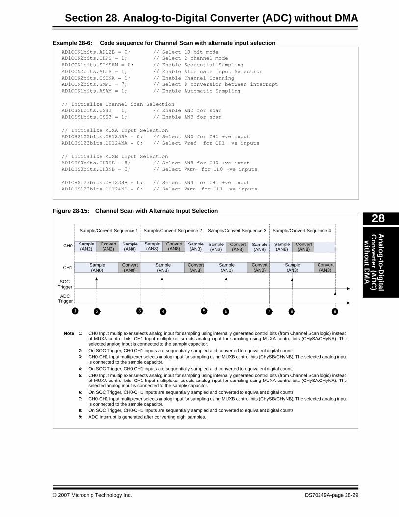
Example 28-6: Code sequence for Channel Scan with alternate input selection
Figure 28-15: Channel Scan with Alternate Input Selection
AD1CON1bits.AD12B = 0; // Select 10-bit modeAD1CON2bits.CHPS = 1; // Select 2-channel modeAD1CON1bits.SIMSAM = 0; // Enable Sequential SamplingAD1CON2bits.ALTS = 1; // Enable Alternate Input SelectionAD1CON2bits.CSCNA = 1; // Enable Channel ScanningAD1CON2bits.SMPI = 7; // Select 8 conversion between interruptAD1CON1bits.ASAM = 1; // Enable Automatic Sampling
// Initialize Channel Scan SelectionAD1CSSLbits.CSS2 = 1; // Enable AN2 for scanAD1CSSLbits.CSS3 = 1; // Enable AN3 for scan
// Initialize MUXA Input SelectionAD1CHS123bits.CH123SA = 0; // Select AN0 for CH1 +ve inputAD1CHS123bits.CH124NA = 0; // Select Vref- for CH1 -ve inputs
// Initialize MUXB Input SelectionAD1CHS0bits.CH0SB = 8; // Select AN8 for CH0 +ve inputAD1CHS0bits.CH0NB = 0; // Select VREF- for CH0 -ve inputs
AD1CHS123bits.CH123SB = 0; // Select AN4 for CH1 +ve inputAD1CHS123bits.CH124NB = 0; // Select VREF- for CH1 -ve inputs
Sample(AN2)
Sample(AN0)
CH0
CH1
Convert(AN2)
Convert (AN0)
SOC Trigger
Sample (AN8)
Sample (AN3)
Convert (AN8)
Convert(AN3)
Sample (AN8)
Sample(AN3)
Sample(AN3)
Sample(AN0)
Convert(AN3)
Convert (AN0)
Sample (AN8)
Sample (AN3)
Convert (AN8)
Convert(AN3)
Sample (AN8)
ADC Trigger
Sample/Convert Sequence 1 Sample/Convert Sequence 2 Sample/Convert Sequence 3 Sample/Convert Sequence 4
1 2 3 4 5 6 7 8 9
Note 1: CH0 Input multiplexer selects analog input for sampling using internally generated control bits (from Channel Scan logic) insteadof MUXA control bits. CH1 Input multiplexer selects analog input for sampling using MUXA control bits (CHySA/CHyNA). Theselected analog input is connected to the sample capacitor.
2: On SOC Trigger, CH0-CH1 inputs are sequentially sampled and converted to equivalent digital counts.3: CH0-CH1 Input multiplexer selects analog input for sampling using MUXB control bits (CHySB/CHyNB). The selected analog input
is connected to the sample capacitor. 4: On SOC Trigger, CH0-CH1 inputs are sequentially sampled and converted to equivalent digital counts.5: CH0 Input multiplexer selects analog input for sampling using internally generated control bits (from Channel Scan logic) instead
of MUXA control bits. CH1 Input multiplexer selects analog input for sampling using MUXA control bits (CHySA/CHyNA). Theselected analog input is connected to the sample capacitor.
6: On SOC Trigger, CH0-CH1 inputs are sequentially sampled and converted to equivalent digital counts.7: CH0-CH1 Input multiplexer selects analog input for sampling using MUXB control bits (CHySB/CHyNB). The selected analog input
is connected to the sample capacitor. 8: On SOC Trigger, CH0-CH1 inputs are sequentially sampled and converted to equivalent digital counts.9: ADC Interrupt is generated after converting eight samples.
© 2007 Microchip Technology Inc. DS70249A-page 28-29

PIC24H Family Reference Manual
28.7 OPERATION DURING SLEEP AND IDLE MODES Sleep and Idle modes are useful for minimizing conversion noise because the digital activity ofthe CPU, buses, and other peripherals is minimized.
28.7.1 CPU Sleep Mode without RC Analog-to-Digital ClockWhen the device enters Sleep mode, all clock sources to the ADC module are shut down andstay at logic ‘0’.
If Sleep occurs in the middle of a conversion, the conversion is aborted unless the ADC isclocked from its internal RC clock generator. The converter does not resume a partiallycompleted conversion on exiting from Sleep mode.
Register contents are not affected by the device entering or leaving Sleep mode.
28.7.2 CPU Sleep Mode with RC Analog-to-Digital ClockThe ADC module can operate during Sleep mode if the analog-to-digital clock source is set tothe internal analog-to-digital RC oscillator (ADRC = 1). This eliminates digital switching noisefrom the conversion. When the conversion is completed, the DONE bit is set and the result isloaded into the ADC Result buffer, ADCBUF.
If enabled, the ADC interrupt wakes up the device from Sleep, and the following occurs:
• If the assigned priority for the interrupt is less than, or equal, to the current CPU priority, the device wakes up and continues code execution from the instruction following the PWRSAV instruction that initiated Sleep mode
• If the assigned priority level for the interrupt source is greater than the current CPU priority, the device wakes up and the CPU exception process begins. Code execution continues from the first instruction of the ADC ISR
The user application should select a conversion trigger source that ensures the analog-to-digitalconversion takes place in Sleep mode. The automatic conversion trigger option can be used forsampling and conversion in Sleep (SSRC<2:0> = 111). To use the automatic conversion option,the ADON bit should be set in the instruction before the PWRSAV instruction.
28.7.3 ADC Operation During CPU Idle ModeWhen the device enters Idle mode, the system clock sources remain functional and the CPUstops executing code. The ADC Stop-in Idle (ADSIDL<13>) bit selection in the ADC Control register (AD1CON1<13>) determines whether the module stops in Idle mode or continues tooperate in Idle mode.
If ICSIDL = 0, the module continues to operate in Idle mode, providing full functionality.
If ICSIDL = 1, the module stops in Idle mode. The module performs the same functions whenstopped in Idle mode as for Sleep mode (refer to 28.7.1 “CPU Sleep Mode without RCAnalog-to-Digital Clock” and 28.7.2 “CPU Sleep Mode with RC Analog-to-Digital Clock”).
Note: For the ADC module to operate in Sleep, the ADC clock source must be set to RC(ADRC = 1).
DS70249A-page 28-30 © 2007 Microchip Technology Inc.

Section 28. Analog-to-Digital Converter (ADC) without DMAA
nalog-to-Digital
Converter (A
DC
) w
ithout DM
A
28
28.8 ANALOG-TO-DIGITAL SAMPLING REQUIREMENTSFigure 28-16 and Figure 28-17 show the analog input model of the 10-bit and 12-bit ADC modes.The total sampling time for the analog-to-digital conversion is a function of the internal amplifiersettling time and the holding capacitor charge time.
For the ADC module to meet its specified accuracy, the charge holding capacitor (CHOLD) mustbe allowed to fully charge to the voltage level on the analog input pin. The analog output sourceimpedance (RS), the interconnect impedance (RIC), and the internal sampling switch (RSS)impedance combine to directly affect the time required to charge the capacitor CHOLD. Thecombined impedance must, therefore, be small enough to fully charge the holding capacitorwithin the chosen sample time. To minimize the effects of pin leakage currents on the accuracyof the ADC module, the maximum recommended source impedance, RS, is 200Ω. After theanalog input channel is selected, this sampling function must be completed prior to starting theconversion. The internal holding capacitor is in a discharged state prior to each sampleoperation.
A minimum time period should be allowed between conversions for the sample time. For moredetails about the minimum sampling time for a device, refer to the “Electrical Specifications” section in the device data sheet.
Figure 28-16: Analog Input Model (10-bit Mode)
Figure 28-17: Analog Input Model (12-bit Mode)
CPINVA
Rs ANxVT = 0.6V
VT = 0.6V I leakage
RIC ≤ 250Ω SamplingSwitch
RSS
CHOLD= DAC capacitance
VSS
VDD
= 4.4 pF± 500 nA
Legend: CPIN
VTI leakage
RICRSS
CHOLD
= input capacitance= threshold voltage= leakage current at the pin due to
= interconnect resistance= sampling switch resistance= Sample/Hold capacitance (from DAC)
various junctions
Note: CPIN value depends on device package and is not tested. Effect of CPIN negligible if Rs ≤ 500 Ω.
RSS ≤ 3 kΩ
CPINVA
Rs ANxVT = 0.6V
VT = 0.6V I leakage
RIC ≤ 250Ω SamplingSwitch
RSS
CHOLD= DAC capacitance
VSS
VDD
= 18 pF± 500 nA
Legend: CPIN
VTI leakage
RICRSS
CHOLD
= input capacitance= threshold voltage= leakage current at the pin due to
= interconnect resistance= sampling switch resistance= Sample/Hold capacitance (from DAC)
various junctions
Note: CPIN value depends on device package and is not tested. Effect of CPIN negligible if Rs ≤ 5 kΩ.
RSS ≤ 3 kΩ
© 2007 Microchip Technology Inc. DS70249A-page 28-31

PIC24H Family Reference Manual
28.8.1 Connection Considerations Since the analog inputs employ ESD protection, they have diodes to VDD and VSS. As a result,the analog input must be between VDD and VSS. If the input voltage exceeds this range by greaterthan 0.3 V in either direction, one of the diodes becomes forward-biased, and it damage thedevice if the input current specification is exceeded.
An external RC filter is sometimes added for anti-aliasing of the input signal. The R componentshould be selected to ensure that the sampling time requirements are satisfied. Any externalcomponents connected (via high-impedance) to an analog input pin (capacitor, Zener diode, etc.)should have very little leakage current at the pin.
DS70249A-page 28-32 © 2007 Microchip Technology Inc.
Section 28. Analog-to-Digital Converter (ADC) without DMAA
nalog-to-Digital
Converter (A
DC
) w
ithout DM
A
28
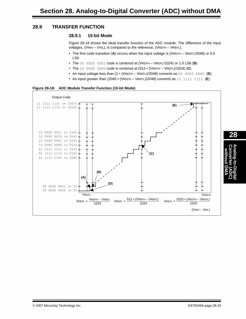
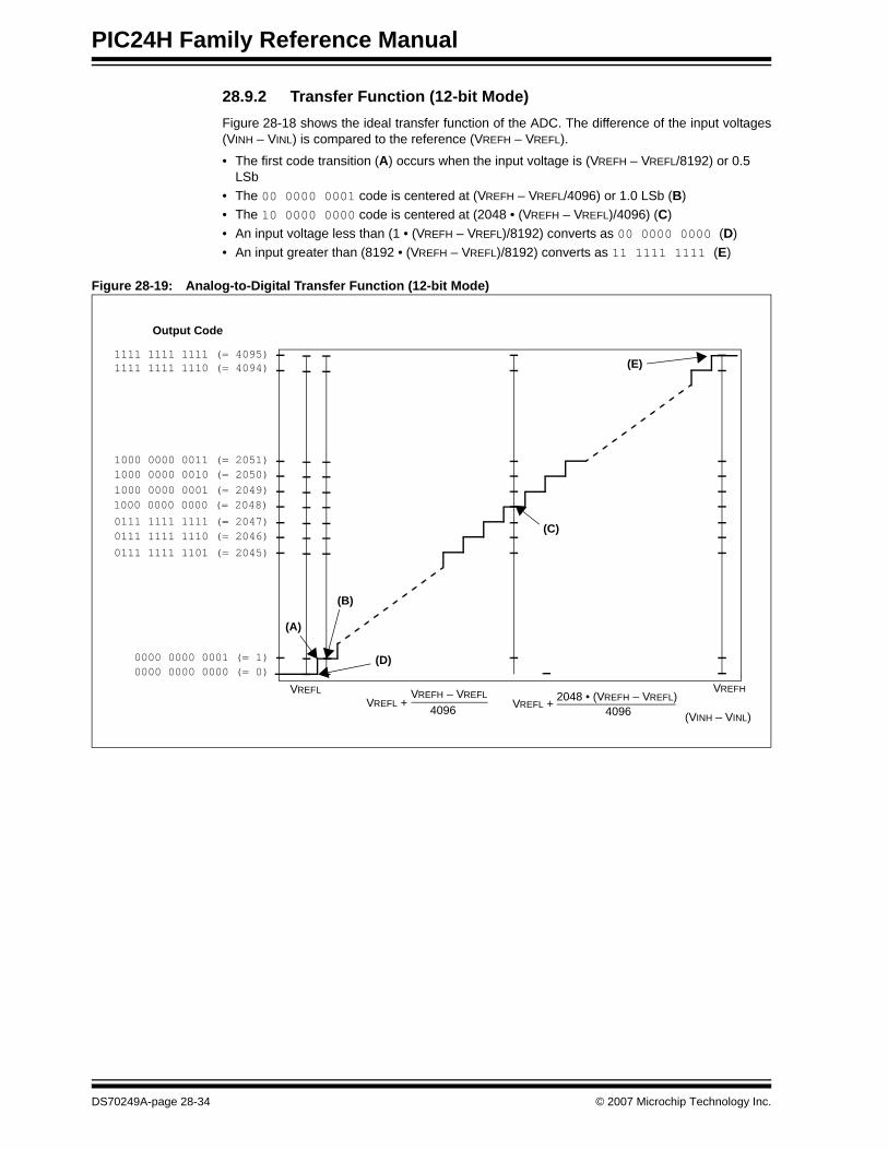
28.9 TRANSFER FUNCTION
28.9.1 10-bit ModeFigure 28-18 shows the ideal transfer function of the ADC module. The difference of the inputvoltages, (VINH – VINL), is compared to the reference, (VREFH – VREFL).
• The first code transition (A) occurs when the input voltage is (VREFH – VREFL/2048) or 0.5 LSb
• The 00 0000 0001 code is centered at (VREFH – VREFL/1024) or 1.0 LSb (B)• The 10 0000 0000 code is centered at (512 • (VREFH – VREFL)/1024) (C)• An input voltage less than (1 • (VREFH – VREFL)/2048) converts as 00 0000 0000 (D)• An input greater than (2045 • (VREFH – VREFL)/2048) converts as 11 1111 1111 (E)
Figure 28-18: ADC Module Transfer Function (10-bit Mode)
10 0000 0010 (= 514)10 0000 0011 (= 515)
01 1111 1101 (= 509)01 1111 1110 (= 510)01 1111 1111 (= 511)
11 1111 1110 (= 1022)11 1111 1111 (= 1023)
00 0000 0000 (= 0)00 0000 0001 (= 1)
Output Code
10 0000 0000 (= 512)
(VINH – VINL)
VREFL
VREFH – VREFL1024
VREFH
VREFL +
10 0000 0001 (= 513)
512 • (VREFH – VREFL)1024
VREFL + 1023 • (VREFH – VREFL)1024
VREFL +
(A)(B)
(C)
(D)
(E)
© 2007 Microchip Technology Inc. DS70249A-page 28-33
PIC24H Family Reference Manual
28.9.2 Transfer Function (12-bit Mode)Figure 28-18 shows the ideal transfer function of the ADC. The difference of the input voltages(VINH – VINL) is compared to the reference (VREFH – VREFL).
• The first code transition (A) occurs when the input voltage is (VREFH – VREFL/8192) or 0.5 LSb
• The 00 0000 0001 code is centered at (VREFH – VREFL/4096) or 1.0 LSb (B)• The 10 0000 0000 code is centered at (2048 • (VREFH – VREFL)/4096) (C)• An input voltage less than (1 • (VREFH – VREFL)/8192) converts as 00 0000 0000 (D)• An input greater than (8192 • (VREFH – VREFL)/8192) converts as 11 1111 1111 (E)
Figure 28-19: Analog-to-Digital Transfer Function (12-bit Mode)
1000 0000 0001 (= 2049)1000 0000 0010 (= 2050)1000 0000 0011 (= 2051)
0111 1111 1101 (= 2045)0111 1111 1110 (= 2046)0111 1111 1111 (= 2047)
1111 1111 1110 (= 4094)1111 1111 1111 (= 4095)
0000 0000 0000 (= 0)0000 0000 0001 (= 1)
Output Code
1000 0000 0000 (= 2048)
(VINH – VINL)
VREFL VREFH – VREFL
4096
VREFHVREFL +
(A)
(B)
(C)
(D)
(E)
2048 • (VREFH – VREFL)4096VREFL +
DS70249A-page 28-34 © 2007 Microchip Technology Inc.

© 2007 M
icrochip Technology Inc.D
S70249A
-page 28-35
Section 28. Analog-to-D
igital Converter (A
DC
) without D
MA
28Th /or bits within a register are read as zeros.
TA
F Bit 3 Bit 2 Bit 1 Bit 0 All Resets
AD xxxx
AD xxxx
AD xxxx
AD xxxx
AD xxxx
AD xxxx
AD xxxx
AD xxxx
AD xxxx
AD xxxx
AD xxxx
AD xxxx
AD xxxx
AD xxxx
AD xxxx
AD xxxx
AD SIMSAM ASAM SAMP DONE 0000
AD <3:0> BUFM ALTS 0000
AD <7:0> 0000
AD — CH123NA<1:0> CH123SA 0000
AD CH0SA<4:0> 0000
AD PCFG3 PCFG2 PCFG1 PCFG0 0000
AD CSS3 CSS2 CSS1 CSS0 0000
Le
Analog-to-Digital Converter (ADC)
without DMA 28
.10 SPECIAL FUNCTION REGISTERSe following table lists the special function registers, including their addresses and formats. All unimplemented registers and
BLE 28-4: ADC REGISTER MAP
ile Name Addr Bit 15 Bit 14 Bit 13 Bit 12 Bit 11 Bit 10 Bit 9 Bit 8 Bit 7 Bit 6 Bit 5 Bit 4
C1BUF0 0300 ADC Data Buffer 0
C1BUF1 0302 ADC Data Buffer 1
C1BUF2 0304 ADC Data Buffer 2
C1BUF3 0306 ADC Data Buffer 3
C1BUF4 0308 ADC Data Buffer 4
C1BUF5 030A ADC Data Buffer 5
C1BUF6 030C ADC Data Buffer 6
C1BUF7 030E ADC Data Buffer 7
C1BUF8 0310 ADC Data Buffer 8
C1BUF9 0312 ADC Data Buffer 9
C1BUFA 0314 ADC Data Buffer 10
C1BUFB 0316 ADC Data Buffer 11
C1BUFC 0318 ADC Data Buffer 12
C1BUFD 031A ADC Data Buffer 13
C1BUFE 031C ADC Data Buffer 14
C1BUFF 031E ADC Data Buffer 15
1CON1 0320 ADON — ADSIDL — — AD12B FORM<1:0> SSRC<2:0> —
1CON2 0322 VCFG<2:0> — — CSCNA CHPS<1:0> BUFS — SMPI
1CON3 0324 ADRC — — SAMC<4:0> ADCS
1CHS123 0326 — — — — — CH123NB<1:0> CH123SB — — — —
1CHS0 0328 CH0NB — — CH0SB<4:0> CH0NA — —
1PCFGL 032C — — — PCFG12 PCFG11 PCFG10 PCFG9 PCFG8 PCFG7 PCFG6 PCFG5 PCFG4
1CSSL 0330 — — — CSS12 CSS11 CSS10 CSS9 CSS8 CSS7 CSS6 CSS5 CSS4
gend: x = unknown value on Reset, — = unimplemented, read as ‘0’. Reset values are shown in hexadecimal.

PIC24H Family Reference Manual
28.11 DESIGN TIPS
Question 1: How can I optimize the system performance of the ADC module? Answer: Here are three suggestions for optimizing performance:
a) Make sure you are meeting all of the timing specifications. If you are turningthe ADC module off and on, there is a minimum delay you must wait beforetaking a sample. If you are changing input channels, there is a minimumdelay you must wait for as well. Also, there is TAD, which is the time selectedfor each bit conversion. TAD is selected in the ADC Control register(AD1CON3) and should be within a range as specified in the “ElectricalCharacteristics” section of the device data sheet. If TAD is too short, the resultmay not be fully converted before the conversion is terminated. If TAD is toolong, the voltage on the sampling capacitor can decay before the conversionis complete. These timing specifications are provided in the “ElectricalSpecifications” section of the device data sheet.
b) Often the source impedance of the analog signal is high (greater than 10kΩ), so the current drawn from the source to charge the sample capacitorcan affect accuracy. If the input signal does not change too quickly, put a 0.1μF capacitor on the analog input. This capacitor charges to the analogvoltage being sampled and supplies the instantaneous current needed tocharge the 4.4 pF internal holding capacitor.
c) Put the device into Sleep mode before the start of the analog-to-digitalconversion. The RC clock source selection is required for conversions inSleep mode. This technique increases accuracy because digital noise fromthe CPU and other peripherals is minimized.
Question 2: Do you know of a good reference on Analog-to-Digital conversion?Answer: A good reference for understanding Analog-to-Digital conversion is the
“Analog-Digital Conversion Handbook”, Third edition, published by Prentice Hall(ISBN 0-13-03-2848-0).
Question 3: My combination of channels/sample and samples/interrupt is greater thanthe size of the buffer. What happens to the buffer in this instance?
Answer: The buffer contains unknown results. This configuration is not recommended.
DS70249A-page 28-36 © 2007 Microchip Technology Inc.
Section 28. Analog-to-Digital Converter (ADC) without DMAA
nalog-to-Digital
Converter (A
DC
) w
ithout DM
A
28
28.12 RELATED APPLICATION NOTESThis section lists application notes that are related to this section of the manual. Theseapplication notes may not be written specifically for the PIC24H device family, but the conceptsare pertinent and could be used with modification and possible limitations. The current application notes related to the Analog-to-Digital Converter (ADC) without DMA module are:
Title Application Note #Using the Analog-to-Digital (A/D) Converter AN546
4-Channel Digital Voltmeter with Display and Keyboard AN557
Understanding A/D Converter Performance Specifications AN693
Using the dsPIC30F for Sensorless BLDC Control AN901
Using the dsPIC30F for Vector Control of an ACIM AN908
Sensored BLDC Motor Control Using the dsPIC30F2010 AN957
An Introduction to AC Induction Motor Control Using the dsPIC30F MCU AN984
Note: For additional application notes and code examples for the PIC24H device family,visit the Microchip website (www.microchip.com).
© 2007 Microchip Technology Inc. DS70249A-page 28-37

PIC24H Family Reference Manual
28.13 REVISION HISTORY
Revision A (June 2007)This is the initial released version of this document.
DS70249A-page 28-38 © 2007 Microchip Technology Inc.
Related Documents