© 2007 Microchip Technology Inc. DS70064E-page 17-1 10-bit A/D Converter 17 Section 17. 10-bit A/D Converter HIGHLIGHTS This section of the manual contains the following major topics: 17.1 Introduction .................................................................................................................. 17-2 17.2 Control Registers ......................................................................................................... 17-4 17.3 A/D Result Buffer ......................................................................................................... 17-4 17.4 A/D Terminology and Conversion Sequence ............................................................. 17-11 17.5 A/D Module Configuration .......................................................................................... 17-13 17.6 Selecting the Voltage Reference Source ................................................................... 17-13 17.7 Selecting the A/D Conversion Clock .......................................................................... 17-13 17.8 Selecting Analog Inputs for Sampling ........................................................................ 17-14 17.9 Enabling the Module .................................................................................................. 17-16 17.10 Specifying the Sample/Conversion Sequence ........................................................... 17-16 17.11 How to Start Sampling ............................................................................................... 17-17 17.12 How to Stop Sampling and Start Conversions ........................................................... 17-18 17.13 Controlling Sample/Conversion Operation................................................................. 17-29 17.14 Specifying How Conversion Results are Written Into the Buffer ................................ 17-30 17.15 Turning the A/D Module Off ....................................................................................... 17-30 17.16 Conversion Sequence Examples ............................................................................... 17-31 17.17 A/D Sampling Requirements...................................................................................... 17-45 17.18 Reading the A/D Result Buffer ................................................................................... 17-46 17.19 Transfer Function ....................................................................................................... 17-47 17.20 A/D Accuracy/Error .................................................................................................... 17-47 17.21 Connection Considerations ........................................................................................ 17-47 17.22 Initialization ................................................................................................................ 17-48 17.23 A/D Conversion Speeds ............................................................................................. 17-49 17.24 Operation During Sleep and Idle Modes .................................................................... 17-55 17.25 Effects of a Reset ....................................................................................................... 17-55 17.26 Special Function Registers Associated with the 10-bit A/D Converter....................... 17-56 17.27 Design Tips ................................................................................................................ 17-57 17.28 Related Application Notes.......................................................................................... 17-58 17.29 Revision History ......................................................................................................... 17-59

Welcome message from author
This document is posted to help you gain knowledge. Please leave a comment to let me know what you think about it! Share it to your friends and learn new things together.
Transcript
Section 17. 10-bit A/D Converter
10-bit A/D
Converter
17
HIGHLIGHTSThis section of the manual contains the following major topics:17.1 Introduction .................................................................................................................. 17-217.2 Control Registers ......................................................................................................... 17-417.3 A/D Result Buffer ......................................................................................................... 17-417.4 A/D Terminology and Conversion Sequence ............................................................. 17-1117.5 A/D Module Configuration.......................................................................................... 17-1317.6 Selecting the Voltage Reference Source ................................................................... 17-1317.7 Selecting the A/D Conversion Clock .......................................................................... 17-1317.8 Selecting Analog Inputs for Sampling ........................................................................ 17-1417.9 Enabling the Module .................................................................................................. 17-1617.10 Specifying the Sample/Conversion Sequence ........................................................... 17-1617.11 How to Start Sampling ............................................................................................... 17-1717.12 How to Stop Sampling and Start Conversions ........................................................... 17-1817.13 Controlling Sample/Conversion Operation................................................................. 17-2917.14 Specifying How Conversion Results are Written Into the Buffer ................................ 17-3017.15 Turning the A/D Module Off ....................................................................................... 17-3017.16 Conversion Sequence Examples............................................................................... 17-3117.17 A/D Sampling Requirements...................................................................................... 17-4517.18 Reading the A/D Result Buffer ................................................................................... 17-4617.19 Transfer Function ....................................................................................................... 17-4717.20 A/D Accuracy/Error .................................................................................................... 17-4717.21 Connection Considerations........................................................................................ 17-4717.22 Initialization ................................................................................................................ 17-4817.23 A/D Conversion Speeds............................................................................................. 17-4917.24 Operation During Sleep and Idle Modes.................................................................... 17-5517.25 Effects of a Reset....................................................................................................... 17-5517.26 Special Function Registers Associated with the 10-bit A/D Converter....................... 17-5617.27 Design Tips ................................................................................................................ 17-5717.28 Related Application Notes.......................................................................................... 17-5817.29 Revision History ......................................................................................................... 17-59
© 2007 Microchip Technology Inc. DS70064E-page 17-1
dsPIC30F Family Reference Manual
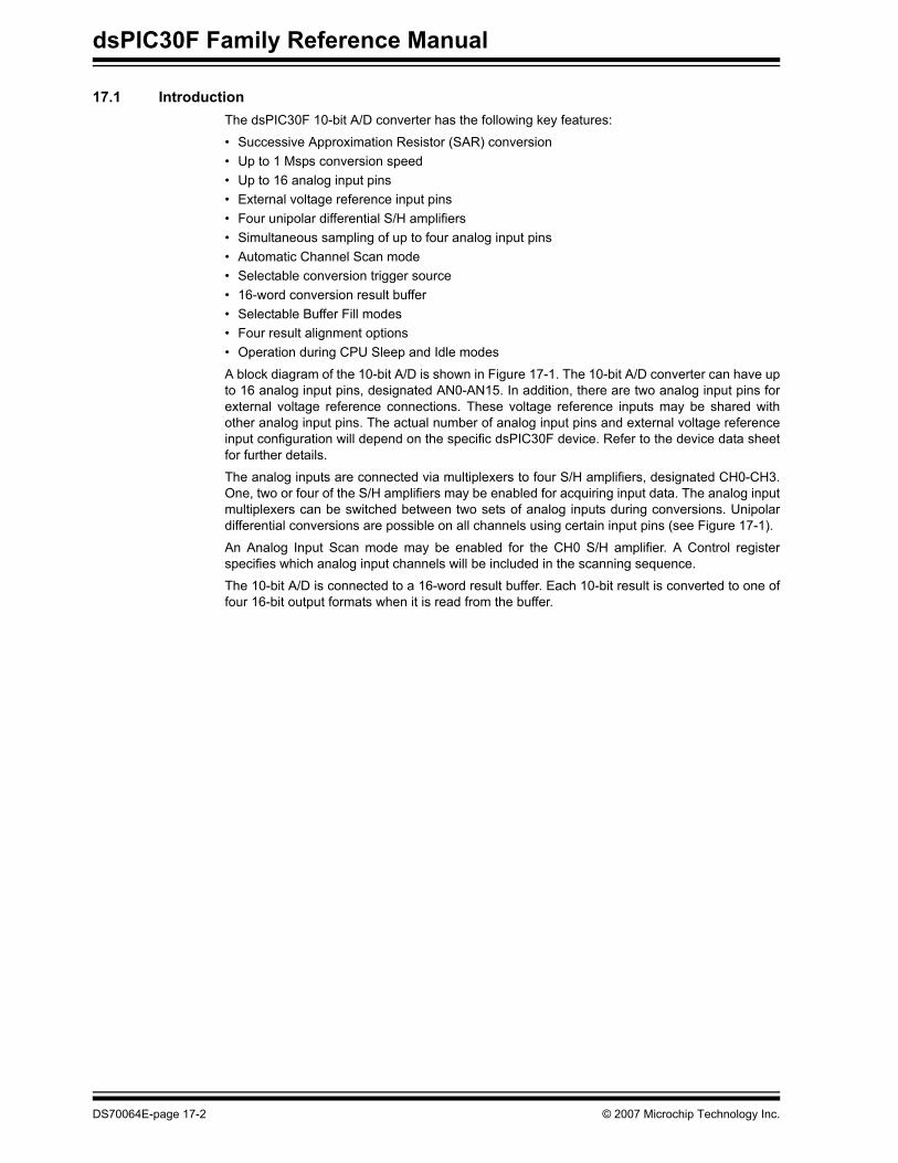
17.1 Introduction The dsPIC30F 10-bit A/D converter has the following key features:
• Successive Approximation Resistor (SAR) conversion• Up to 1 Msps conversion speed• Up to 16 analog input pins• External voltage reference input pins• Four unipolar differential S/H amplifiers • Simultaneous sampling of up to four analog input pins• Automatic Channel Scan mode• Selectable conversion trigger source• 16-word conversion result buffer• Selectable Buffer Fill modes• Four result alignment options • Operation during CPU Sleep and Idle modes
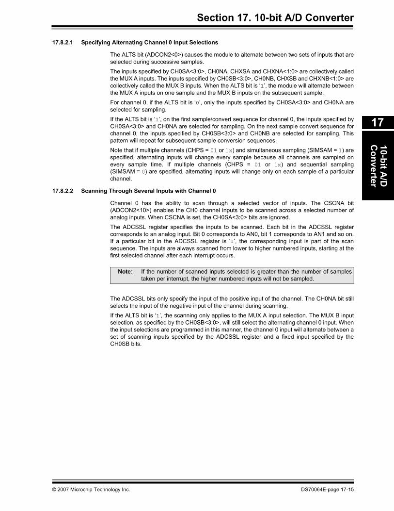
A block diagram of the 10-bit A/D is shown in Figure 17-1. The 10-bit A/D converter can have upto 16 analog input pins, designated AN0-AN15. In addition, there are two analog input pins forexternal voltage reference connections. These voltage reference inputs may be shared withother analog input pins. The actual number of analog input pins and external voltage referenceinput configuration will depend on the specific dsPIC30F device. Refer to the device data sheetfor further details.
The analog inputs are connected via multiplexers to four S/H amplifiers, designated CH0-CH3.One, two or four of the S/H amplifiers may be enabled for acquiring input data. The analog inputmultiplexers can be switched between two sets of analog inputs during conversions. Unipolardifferential conversions are possible on all channels using certain input pins (see Figure 17-1).
An Analog Input Scan mode may be enabled for the CH0 S/H amplifier. A Control registerspecifies which analog input channels will be included in the scanning sequence.
The 10-bit A/D is connected to a 16-word result buffer. Each 10-bit result is converted to one offour 16-bit output formats when it is read from the buffer.
DS70064E-page 17-2 © 2007 Microchip Technology Inc.

Section 17. 10-bit A/D Converter10-bit A
/DC
onverter
17
Figure 17-1: 10-Bit High-Speed A/D Block Diagram
S/H+
-
10-bit Result Conversion Logic
VREF+AVSS
AVDD
ADC
Dat
a Fo
rmat
16-word, 10-bitDual Port
RAM
Bus
Inte
rface
AN12
0000
0101
0111
1001
1101
1110
1111
1100
000100100011
0100
0110
1000
1010
1011
AN13
AN14
AN15
AN8
AN9
AN10
AN11
AN2
AN4
AN7
AN0
AN3
AN1
AN5
CH1
CH2
CH3
CH0
AN5AN2
AN11AN8
VREF-
AN4AN1
AN10AN7
VREF-
AN3AN0
AN9AN6
VREF-
AN1VREF-
VREF-
Sample/SequenceControlSample
CH1,CH2,CH3,CH0
Input MUXControl
InputSwitches
S/H+
-
S/H+
-
S/H+
-
AN6
Note: VREF+, VREF- inputs may be shared with other analog inputs. See device data sheet for details.
© 2007 Microchip Technology Inc. DS70064E-page 17-3
dsPIC30F Family Reference Manual
17.2 Control RegistersThe A/D module has six Control and Status registers. These registers are:
• ADCON1: A/D Control Register 1• ADCON2: A/D Control Register 2• ADCON3: A/D Control Register 3• ADCHS: A/D Input Channel Select Register• ADPCFG: A/D Port Configuration Register• ADCSSL: A/D Input Scan Select Register
The ADCON1, ADCON2 and ADCON3 registers control the operation of the A/D module. TheADCHS register selects the input pins to be connected to the S/H amplifiers. The ADPCFGregister configures the analog input pins as analog inputs or as digital I/O. The ADCSSL registerselects inputs to be sequentially scanned.
17.3 A/D Result BufferThe module contains a 16-word dual port RAM, called ADCBUF, to buffer the A/D results. The16 buffer locations are referred to as ADCBUF0, ADCBUF1, ADCBUF2, ...., ADCBUFE,ADCBUFF.
Note: The A/D result buffer is a read only buffer.
DS70064E-page 17-4 © 2007 Microchip Technology Inc.
Section 17. 10-bit A/D Converter10-bit A
/DC
onverter
17
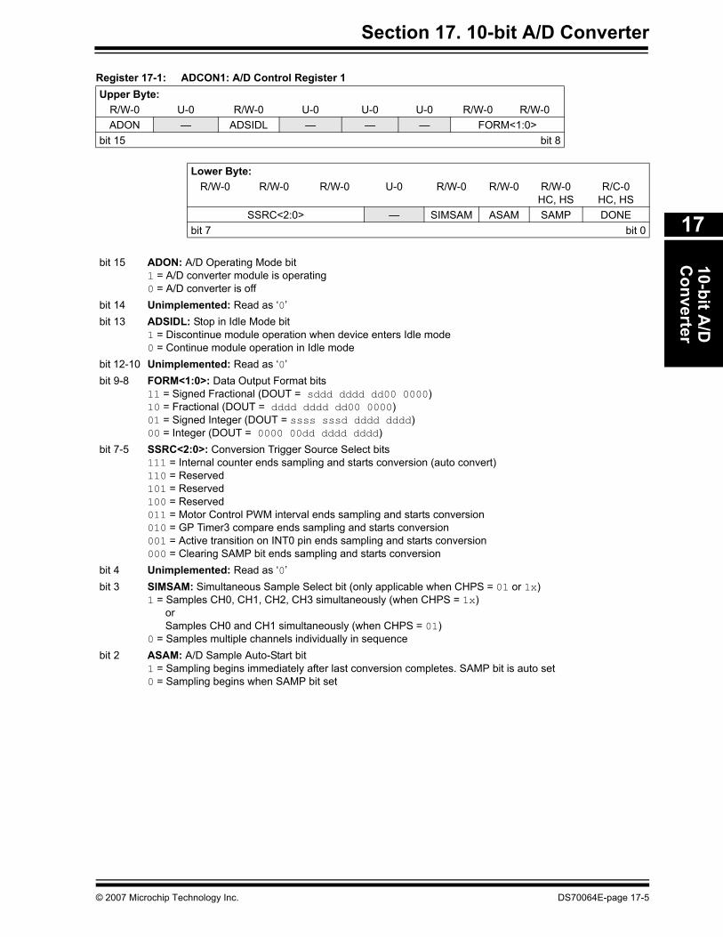
Register 17-1: ADCON1: A/D Control Register 1Upper Byte:
R/W-0 U-0 R/W-0 U-0 U-0 U-0 R/W-0 R/W-0ADON — ADSIDL — — — FORM<1:0>
bit 15 bit 8
Lower Byte:R/W-0 R/W-0 R/W-0 U-0 R/W-0 R/W-0 R/W-0
HC, HSR/C-0
HC, HSSSRC<2:0> — SIMSAM ASAM SAMP DONE
bit 7 bit 0
bit 15 ADON: A/D Operating Mode bit1 = A/D converter module is operating0 = A/D converter is off
bit 14 Unimplemented: Read as ‘0’bit 13 ADSIDL: Stop in Idle Mode bit
1 = Discontinue module operation when device enters Idle mode0 = Continue module operation in Idle mode
bit 12-10 Unimplemented: Read as ‘0’bit 9-8 FORM<1:0>: Data Output Format bits
11 = Signed Fractional (DOUT = sddd dddd dd00 0000)10 = Fractional (DOUT = dddd dddd dd00 0000)01 = Signed Integer (DOUT = ssss sssd dddd dddd)00 = Integer (DOUT = 0000 00dd dddd dddd)
bit 7-5 SSRC<2:0>: Conversion Trigger Source Select bits111 = Internal counter ends sampling and starts conversion (auto convert)110 = Reserved101 = Reserved100 = Reserved011 = Motor Control PWM interval ends sampling and starts conversion010 = GP Timer3 compare ends sampling and starts conversion001 = Active transition on INT0 pin ends sampling and starts conversion000 = Clearing SAMP bit ends sampling and starts conversion
bit 4 Unimplemented: Read as ‘0’bit 3 SIMSAM: Simultaneous Sample Select bit (only applicable when CHPS = 01 or 1x)
1 = Samples CH0, CH1, CH2, CH3 simultaneously (when CHPS = 1x)orSamples CH0 and CH1 simultaneously (when CHPS = 01)
0 = Samples multiple channels individually in sequencebit 2 ASAM: A/D Sample Auto-Start bit
1 = Sampling begins immediately after last conversion completes. SAMP bit is auto set0 = Sampling begins when SAMP bit set
© 2007 Microchip Technology Inc. DS70064E-page 17-5
dsPIC30F Family Reference Manual
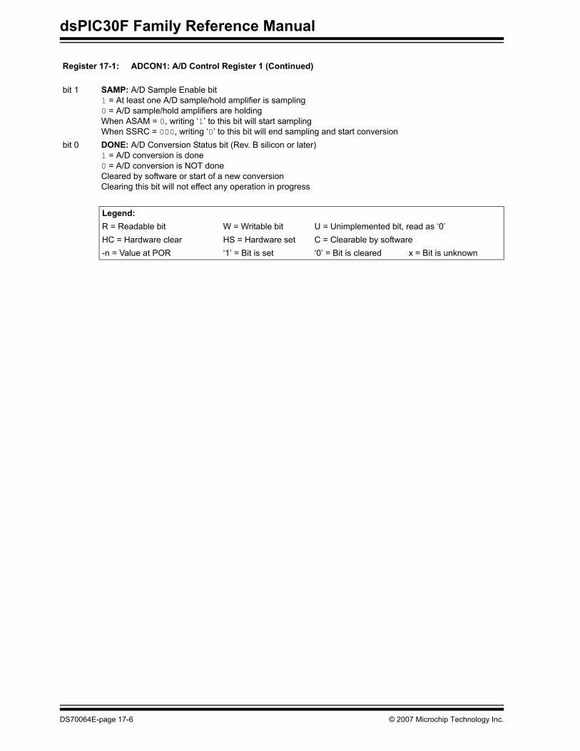
Register 17-1: ADCON1: A/D Control Register 1 (Continued)
bit 1 SAMP: A/D Sample Enable bit1 = At least one A/D sample/hold amplifier is sampling0 = A/D sample/hold amplifiers are holdingWhen ASAM = 0, writing ‘1’ to this bit will start samplingWhen SSRC = 000, writing ‘0’ to this bit will end sampling and start conversion
bit 0 DONE: A/D Conversion Status bit (Rev. B silicon or later)1 = A/D conversion is done0 = A/D conversion is NOT doneCleared by software or start of a new conversionClearing this bit will not effect any operation in progress
Legend:R = Readable bit W = Writable bit U = Unimplemented bit, read as ‘0’HC = Hardware clear HS = Hardware set C = Clearable by software-n = Value at POR ‘1’ = Bit is set ‘0’ = Bit is cleared x = Bit is unknown
DS70064E-page 17-6 © 2007 Microchip Technology Inc.
Section 17. 10-bit A/D Converter10-bit A
/DC
onverter
17
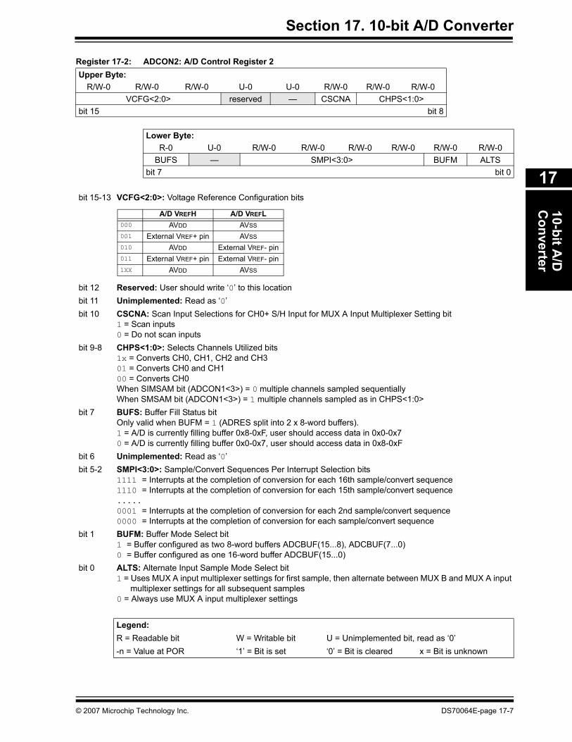
Register 17-2: ADCON2: A/D Control Register 2 Upper Byte:
R/W-0 R/W-0 R/W-0 U-0 U-0 R/W-0 R/W-0 R/W-0VCFG<2:0> reserved — CSCNA CHPS<1:0>
bit 15 bit 8
Lower Byte:R-0 U-0 R/W-0 R/W-0 R/W-0 R/W-0 R/W-0 R/W-0
BUFS — SMPI<3:0> BUFM ALTSbit 7 bit 0
bit 15-13 VCFG<2:0>: Voltage Reference Configuration bits
bit 12 Reserved: User should write ‘0’ to this locationbit 11 Unimplemented: Read as ‘0’bit 10 CSCNA: Scan Input Selections for CH0+ S/H Input for MUX A Input Multiplexer Setting bit
1 = Scan inputs0 = Do not scan inputs
bit 9-8 CHPS<1:0>: Selects Channels Utilized bits1x = Converts CH0, CH1, CH2 and CH301 = Converts CH0 and CH100 = Converts CH0When SIMSAM bit (ADCON1<3>) = 0 multiple channels sampled sequentiallyWhen SMSAM bit (ADCON1<3>) = 1 multiple channels sampled as in CHPS<1:0>
bit 7 BUFS: Buffer Fill Status bitOnly valid when BUFM = 1 (ADRES split into 2 x 8-word buffers).1 = A/D is currently filling buffer 0x8-0xF, user should access data in 0x0-0x70 = A/D is currently filling buffer 0x0-0x7, user should access data in 0x8-0xF
bit 6 Unimplemented: Read as ‘0’bit 5-2 SMPI<3:0>: Sample/Convert Sequences Per Interrupt Selection bits
1111 = Interrupts at the completion of conversion for each 16th sample/convert sequence1110 = Interrupts at the completion of conversion for each 15th sample/convert sequence.....0001 = Interrupts at the completion of conversion for each 2nd sample/convert sequence0000 = Interrupts at the completion of conversion for each sample/convert sequence
bit 1 BUFM: Buffer Mode Select bit1 = Buffer configured as two 8-word buffers ADCBUF(15...8), ADCBUF(7...0)0 = Buffer configured as one 16-word buffer ADCBUF(15...0)
bit 0 ALTS: Alternate Input Sample Mode Select bit1 = Uses MUX A input multiplexer settings for first sample, then alternate between MUX B and MUX A input
multiplexer settings for all subsequent samples0 = Always use MUX A input multiplexer settings
Legend:R = Readable bit W = Writable bit U = Unimplemented bit, read as ‘0’-n = Value at POR ‘1’ = Bit is set ‘0’ = Bit is cleared x = Bit is unknown
A/D VREFH A/D VREFL000 AVDD AVSS
001 External VREF+ pin AVSS
010 AVDD External VREF- pin011 External VREF+ pin External VREF- pin1XX AVDD AVSS
© 2007 Microchip Technology Inc. DS70064E-page 17-7
dsPIC30F Family Reference Manual
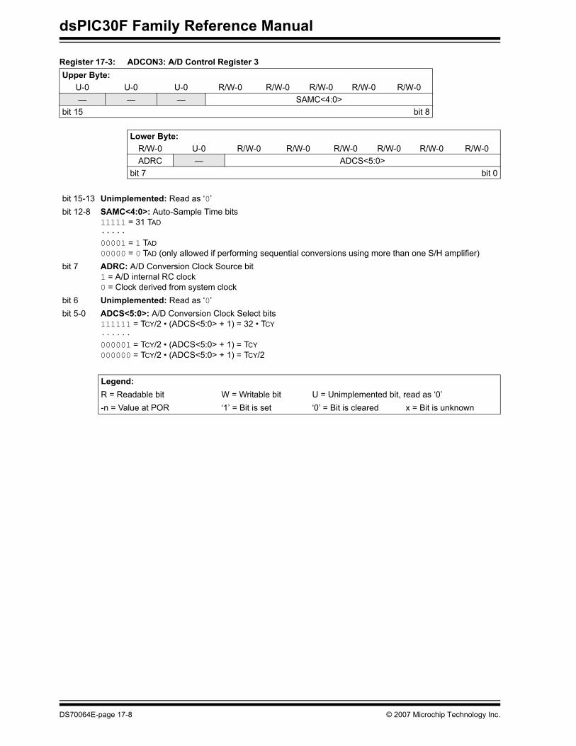
Register 17-3: ADCON3: A/D Control Register 3 Upper Byte:
U-0 U-0 U-0 R/W-0 R/W-0 R/W-0 R/W-0 R/W-0— — — SAMC<4:0>
bit 15 bit 8
Lower Byte:R/W-0 U-0 R/W-0 R/W-0 R/W-0 R/W-0 R/W-0 R/W-0ADRC — ADCS<5:0>
bit 7 bit 0
bit 15-13 Unimplemented: Read as ‘0’bit 12-8 SAMC<4:0>: Auto-Sample Time bits
11111 = 31 TAD·····00001 = 1 TAD00000 = 0 TAD (only allowed if performing sequential conversions using more than one S/H amplifier)
bit 7 ADRC: A/D Conversion Clock Source bit1 = A/D internal RC clock0 = Clock derived from system clock
bit 6 Unimplemented: Read as ‘0’bit 5-0 ADCS<5:0>: A/D Conversion Clock Select bits
111111 = TCY/2 • (ADCS<5:0> + 1) = 32 • TCY······000001 = TCY/2 • (ADCS<5:0> + 1) = TCY000000 = TCY/2 • (ADCS<5:0> + 1) = TCY/2
Legend:R = Readable bit W = Writable bit U = Unimplemented bit, read as ‘0’-n = Value at POR ‘1’ = Bit is set ‘0’ = Bit is cleared x = Bit is unknown
DS70064E-page 17-8 © 2007 Microchip Technology Inc.
Section 17. 10-bit A/D Converter10-bit A
/DC
onverter
17
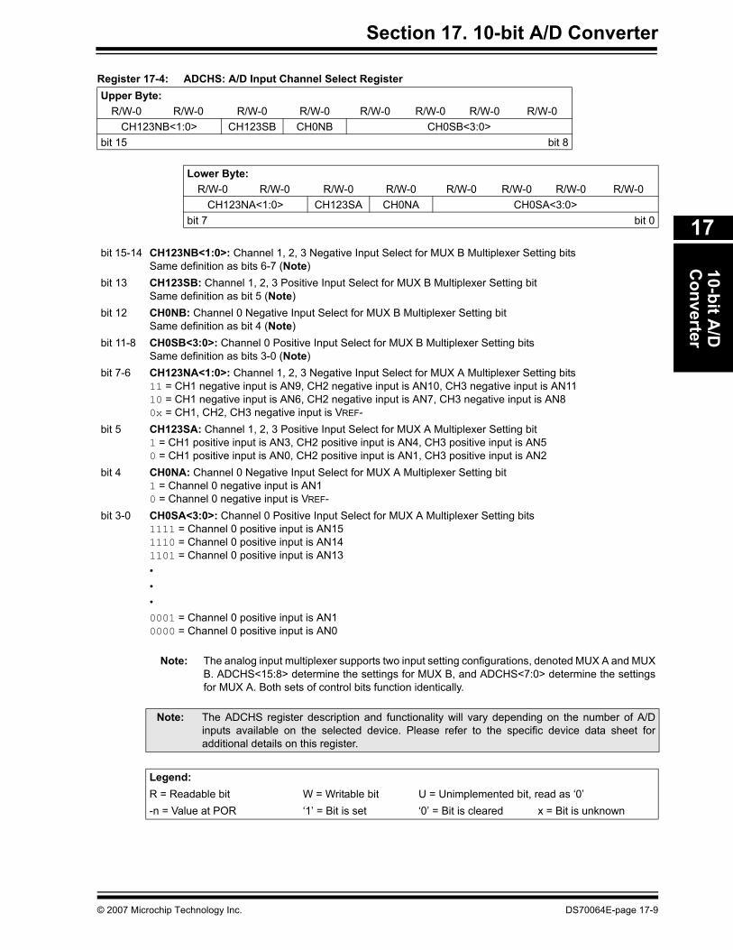
Register 17-4: ADCHS: A/D Input Channel Select Register Upper Byte:
R/W-0 R/W-0 R/W-0 R/W-0 R/W-0 R/W-0 R/W-0 R/W-0CH123NB<1:0> CH123SB CH0NB CH0SB<3:0>
bit 15 bit 8
Lower Byte:R/W-0 R/W-0 R/W-0 R/W-0 R/W-0 R/W-0 R/W-0 R/W-0
CH123NA<1:0> CH123SA CH0NA CH0SA<3:0>bit 7 bit 0
bit 15-14 CH123NB<1:0>: Channel 1, 2, 3 Negative Input Select for MUX B Multiplexer Setting bitsSame definition as bits 6-7 (Note)
bit 13 CH123SB: Channel 1, 2, 3 Positive Input Select for MUX B Multiplexer Setting bitSame definition as bit 5 (Note)
bit 12 CH0NB: Channel 0 Negative Input Select for MUX B Multiplexer Setting bitSame definition as bit 4 (Note)
bit 11-8 CH0SB<3:0>: Channel 0 Positive Input Select for MUX B Multiplexer Setting bitsSame definition as bits 3-0 (Note)
bit 7-6 CH123NA<1:0>: Channel 1, 2, 3 Negative Input Select for MUX A Multiplexer Setting bits11 = CH1 negative input is AN9, CH2 negative input is AN10, CH3 negative input is AN1110 = CH1 negative input is AN6, CH2 negative input is AN7, CH3 negative input is AN80x = CH1, CH2, CH3 negative input is VREF-
bit 5 CH123SA: Channel 1, 2, 3 Positive Input Select for MUX A Multiplexer Setting bit1 = CH1 positive input is AN3, CH2 positive input is AN4, CH3 positive input is AN50 = CH1 positive input is AN0, CH2 positive input is AN1, CH3 positive input is AN2
bit 4 CH0NA: Channel 0 Negative Input Select for MUX A Multiplexer Setting bit1 = Channel 0 negative input is AN10 = Channel 0 negative input is VREF-
bit 3-0 CH0SA<3:0>: Channel 0 Positive Input Select for MUX A Multiplexer Setting bits1111 = Channel 0 positive input is AN151110 = Channel 0 positive input is AN141101 = Channel 0 positive input is AN13•••0001 = Channel 0 positive input is AN10000 = Channel 0 positive input is AN0
Note: The analog input multiplexer supports two input setting configurations, denoted MUX A and MUXB. ADCHS<15:8> determine the settings for MUX B, and ADCHS<7:0> determine the settingsfor MUX A. Both sets of control bits function identically.
Note: The ADCHS register description and functionality will vary depending on the number of A/Dinputs available on the selected device. Please refer to the specific device data sheet foradditional details on this register.
Legend:R = Readable bit W = Writable bit U = Unimplemented bit, read as ‘0’-n = Value at POR ‘1’ = Bit is set ‘0’ = Bit is cleared x = Bit is unknown
© 2007 Microchip Technology Inc. DS70064E-page 17-9
dsPIC30F Family Reference Manual
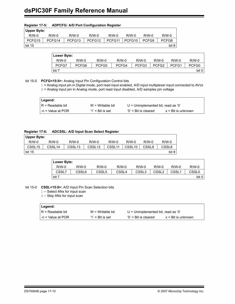
Register 17-5: ADPCFG: A/D Port Configuration Register
Register 17-6: ADCSSL: A/D Input Scan Select Register
Upper Byte:R/W-0 R/W-0 R/W-0 R/W-0 R/W-0 R/W-0 R/W-0 R/W-0
PCFG15 PCFG14 PCFG13 PCFG12 PCFG11 PCFG10 PCFG9 PCFG8bit 15 bit 8
Lower Byte:R/W-0 R/W-0 R/W-0 R/W-0 R/W-0 R/W-0 R/W-0 R/W-0PCFG7 PCFG6 PCFG5 PCFG4 PCFG3 PCFG2 PCFG1 PCFG0
bit 7 bit 0
bit 15-0 PCFG<15:0>: Analog Input Pin Configuration Control bits1 = Analog input pin in Digital mode, port read input enabled, A/D input multiplexer input connected to AVSS0 = Analog input pin in Analog mode, port read input disabled, A/D samples pin voltage
Legend:R = Readable bit W = Writable bit U = Unimplemented bit, read as ‘0’-n = Value at POR ‘1’ = Bit is set ‘0’ = Bit is cleared x = Bit is unknown
Upper Byte:R/W-0 R/W-0 R/W-0 R/W-0 R/W-0 R/W-0 R/W-0 R/W-0
CSSL15 CSSL14 CSSL13 CSSL12 CSSL11 CSSL10 CSSL9 CSSL8bit 15 bit 8
Lower Byte:R/W-0 R/W-0 R/W-0 R/W-0 R/W-0 R/W-0 R/W-0 R/W-0CSSL7 CSSL6 CSSL5 CSSL4 CSSL3 CSSL2 CSSL1 CSSL0
bit 7 bit 0
bit 15-0 CSSL<15:0>: A/D Input Pin Scan Selection bits1 = Select ANx for input scan0 = Skip ANx for input scan
Legend:R = Readable bit W = Writable bit U = Unimplemented bit, read as ‘0’-n = Value at POR ‘1’ = Bit is set ‘0’ = Bit is cleared x = Bit is unknown
DS70064E-page 17-10 © 2007 Microchip Technology Inc.
Section 17. 10-bit A/D Converter10-bit A
/DC
onverter
17
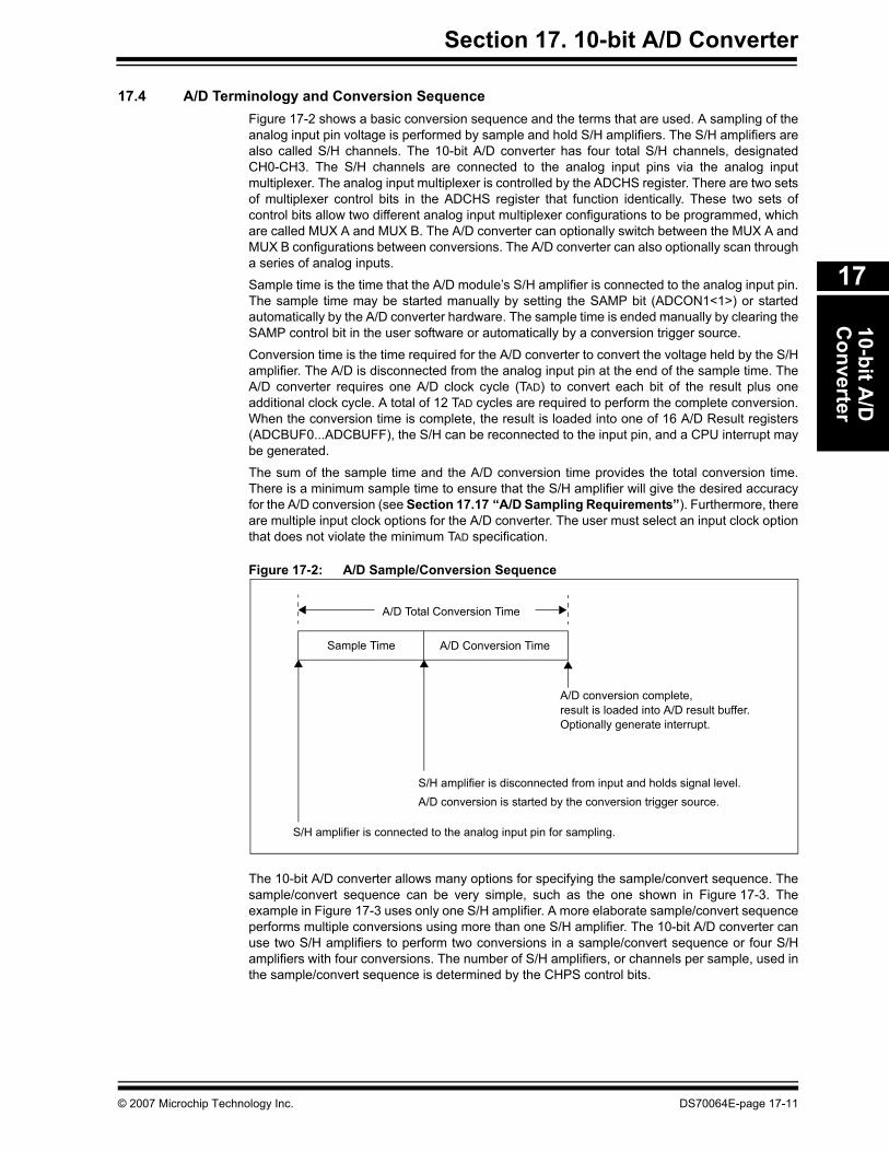
17.4 A/D Terminology and Conversion SequenceFigure 17-2 shows a basic conversion sequence and the terms that are used. A sampling of theanalog input pin voltage is performed by sample and hold S/H amplifiers. The S/H amplifiers arealso called S/H channels. The 10-bit A/D converter has four total S/H channels, designatedCH0-CH3. The S/H channels are connected to the analog input pins via the analog inputmultiplexer. The analog input multiplexer is controlled by the ADCHS register. There are two setsof multiplexer control bits in the ADCHS register that function identically. These two sets ofcontrol bits allow two different analog input multiplexer configurations to be programmed, whichare called MUX A and MUX B. The A/D converter can optionally switch between the MUX A andMUX B configurations between conversions. The A/D converter can also optionally scan througha series of analog inputs.
Sample time is the time that the A/D module’s S/H amplifier is connected to the analog input pin.The sample time may be started manually by setting the SAMP bit (ADCON1<1>) or startedautomatically by the A/D converter hardware. The sample time is ended manually by clearing theSAMP control bit in the user software or automatically by a conversion trigger source.
Conversion time is the time required for the A/D converter to convert the voltage held by the S/Hamplifier. The A/D is disconnected from the analog input pin at the end of the sample time. TheA/D converter requires one A/D clock cycle (TAD) to convert each bit of the result plus oneadditional clock cycle. A total of 12 TAD cycles are required to perform the complete conversion.When the conversion time is complete, the result is loaded into one of 16 A/D Result registers(ADCBUF0...ADCBUFF), the S/H can be reconnected to the input pin, and a CPU interrupt maybe generated.
The sum of the sample time and the A/D conversion time provides the total conversion time.There is a minimum sample time to ensure that the S/H amplifier will give the desired accuracyfor the A/D conversion (see Section 17.17 “A/D Sampling Requirements”). Furthermore, thereare multiple input clock options for the A/D converter. The user must select an input clock optionthat does not violate the minimum TAD specification.
Figure 17-2: A/D Sample/Conversion Sequence
The 10-bit A/D converter allows many options for specifying the sample/convert sequence. Thesample/convert sequence can be very simple, such as the one shown in Figure 17-3. Theexample in Figure 17-3 uses only one S/H amplifier. A more elaborate sample/convert sequenceperforms multiple conversions using more than one S/H amplifier. The 10-bit A/D converter canuse two S/H amplifiers to perform two conversions in a sample/convert sequence or four S/Hamplifiers with four conversions. The number of S/H amplifiers, or channels per sample, used inthe sample/convert sequence is determined by the CHPS control bits.
Sample Time A/D Conversion Time
A/D Total Conversion Time
S/H amplifier is connected to the analog input pin for sampling.
S/H amplifier is disconnected from input and holds signal level.A/D conversion is started by the conversion trigger source.
A/D conversion complete, result is loaded into A/D result buffer. Optionally generate interrupt.
© 2007 Microchip Technology Inc. DS70064E-page 17-11

dsPIC30F Family Reference Manual
A sample/convert sequence that uses multiple S/H channels can be simultaneously sampled orsequentially sampled, as controlled by the SIMSAM bit (ADCON1<3>). Simultaneously samplingmultiple signals ensures that the snapshot of the analog inputs occurs at precisely the same timefor all inputs. Sequential sampling takes a snapshot of each analog input just before conversionstarts on that input, and the sampling of multiple inputs is not correlated.
Figure 17-3: Simultaneous and Sequential Sampling
The start time for sampling can be controlled in software by setting the SAMP control bit. Thestart of the sampling time can also be controlled automatically by the hardware. When the A/Dconverter operates in the Auto-Sample mode, the S/H amplifier(s) is reconnected to the analoginput pin at the end of the conversion in the sample/convert sequence. The auto-sample functionis controlled by the ASAM control bit (ADCON1<2>).
The conversion trigger source ends the sampling time and begins an A/D conversion or asample/convert sequence. The conversion trigger source is selected by the SSRC control bits.The conversion trigger can be taken from a variety of hardware sources, or can be controlledmanually in software by clearing the SAMP control bit. One of the conversion trigger sources isan auto-conversion. The time between auto-conversions is set by a counter and the A/D clock.The Auto-Sample mode and auto-conversion trigger can be used together to provide endlessautomatic conversions without software intervention.
An interrupt may be generated at the end of each sample/convert sequence or multiplesample/convert sequences as determined by the value of the SMPI control bits ADCON2<5:2>.The number of sample/convert sequences between interrupts can vary between 1 and 16. Theuser should note that the A/D conversion buffer holds 16 results when the SMPI value is selected.The total number of conversion results between interrupts is the product of the channels persample and the SMPI value. The total number of conversions between interrupts should notexceed the buffer length.
AN0
AN1
AN2
AN3
SimultaneousSampling
SequentialSampling
DS70064E-page 17-12 © 2007 Microchip Technology Inc.
Section 17. 10-bit A/D Converter10-bit A
/DC
onverter
17
17.5 A/D Module ConfigurationThe following steps should be followed for performing an A/D conversion:
1. Configure the A/D module• Select port pins as analog inputs ADPCFG<15:0>• Select voltage reference source to match expected range on analog inputs
ADCON2<15:13>• Select the analog conversion clock to match desired data rate with processor clock
ADCON3<5:0>• Determine how many S/H channels will be used ADCON2<9:8> and ADPCFG<15:0>• Determine how sampling will occur ADCON1<3> and ADCSSL<15:0>• Determine how inputs will be allocated to S/H channels ADCHS<15:0>• Select the appropriate sample/conversion sequence ADCON1<7:0> and
ADCON3<12:8>• Select how conversion results are presented in the buffer ADCON1<9:8>• Select interrupt rate ADCON2<5:9>• Turn on A/D module ADCON1<15>
2. Configure A/D interrupt (if required)• Clear ADIF bit • Select A/D interrupt priority
The options for each configuration step are described in the subsequent sections.
17.6 Selecting the Voltage Reference SourceThe voltage references for A/D conversions are selected using the VCFG<2:0> control bits(ADCON2<15:13>). The upper voltage reference (VREFH) and the lower voltage reference(VREFL) may be the internal AVDD and AVSS voltage rails or the VREF+ and VREF- input pins.
The external voltage reference pins may be shared with the AN0 and AN1 inputs on low pin countdevices. The A/D converter can still perform conversions on these pins when they are sharedwith the VREF+ and VREF- input pins.
The voltages applied to the external reference pins must meet certain specifications. Refer to the“Electrical Specifications” section of the device data sheet for further details.
17.7 Selecting the A/D Conversion ClockThe A/D converter has a maximum rate at which conversions may be completed. An analogmodule clock, TAD, controls the conversion timing. The A/D conversion requires 12 clock periods(12 TAD). The A/D clock is derived from the device instruction clock or internal RC clock source.
The period of the A/D conversion clock is software selected using a six-bit counter. There are 64possible options for TAD, specified by the ADCS<5:0> bits (ADCON3<5:0>). Equation 17-1 givesthe TAD value as a function of the ADCS control bits and the device instruction cycle clock period,TCY.
Equation 17-1: A/D Conversion Clock Period
For correct A/D conversions, the A/D conversion clock (TAD) must be selected to ensure aminimum TAD time of 83.33 nsec (see Section 17.23 “A/D Conversion Speeds” for furtherdetails).
Note: External VREF+ and VREF- must be selected for conversion rates above 500 ksps.See Section 17.23 “A/D Conversion Speeds” for further details.
TAD = TCY(ADCS + 1)2
ADCS = 2TAD
TCY– 1
© 2007 Microchip Technology Inc. DS70064E-page 17-13
dsPIC30F Family Reference Manual
The A/D converter has a dedicated internal RC clock source that can be used to performconversions. The internal RC clock source should be used when A/D conversions are performedwhile the dsPIC30F is in Sleep mode. The internal RC oscillator is selected by setting the ADRCbit (ADCON3<7>). When the ADRC bit is set, the ADCS<5:0> bits have no effect on the A/Doperation.
17.8 Selecting Analog Inputs for SamplingAll Sample-and-Hold Amplifiers have analog multiplexers (see Figure 17-1) on both theirnon-inverting and inverting inputs to select which analog input(s) are sampled. Once thesample/convert sequence is specified, the ADCHS bits determine which analog inputs areselected for each sample.
Additionally, the selected inputs may vary on an alternating sample basis or may vary on arepeated sequence of samples.
The same analog input can be connected to two or more sample and hold channels to improveconversion rates.
17.8.1 Configuring Analog Port Pins
The ADPCFG register specifies the input condition of device pins used as analog inputs.
A pin is configured as analog input when the corresponding PCFGn bit (ADPCFG<n>) is clear.The ADPCFG register is clear at Reset, causing the A/D input pins to be configured for analoginput by default at Reset.
When configured for analog input, the associated port I/O digital input buffer is disabled so it doesnot consume current.
The ADPCFG register and the TRISB register control the operation of the A/D port pins.
The port pins that are desired as analog inputs must have their corresponding TRIS bit set,specifying port input. If the I/O pin associated with an A/D input is configured as an output, TRISbit is cleared and the ports digital output level (VOH or VOL) will be converted. After a deviceReset, all TRIS bits are set.
A pin is configured as digital I/O when the corresponding PCFGn bit (ADPCFG<n>) is set. In thisconfiguration, the input to the analog multiplexer is connected to AVSS.
17.8.2 Channel 0 Input Selection
Channel 0 is the most flexible of the 4 S/H channels in terms of selecting analog inputs.
The user may select any of the up to 16 analog inputs as the input to the positive input of thechannel. The CH0SA<3:0> bits (ADCHS<3:0>) normally select the analog input for the positiveinput of channel 0.
The user may select either VREF- or AN1 as the negative input of the channel. The CH0NA bit(ADCHS<4>) normally selects the analog input for the negative input of channel 0.
Note: Different devices will have different numbers of analog inputs. Verify the analoginput availability against the device data sheet.
Note 1: When reading the A/D Port register, any pin configured as an analog input reads asa ‘0’.
2: Analog levels on any pin that is defined as a digital input (including the AN15:AN0pins) may cause the input buffer to consume current that is out of the device’sspecification.
DS70064E-page 17-14 © 2007 Microchip Technology Inc.
Section 17. 10-bit A/D Converter10-bit A
/DC
onverter
17
17.8.2.1 Specifying Alternating Channel 0 Input Selections
The ALTS bit (ADCON2<0>) causes the module to alternate between two sets of inputs that areselected during successive samples.
The inputs specified by CH0SA<3:0>, CH0NA, CHXSA and CHXNA<1:0> are collectively calledthe MUX A inputs. The inputs specified by CH0SB<3:0>, CH0NB, CHXSB and CHXNB<1:0> arecollectively called the MUX B inputs. When the ALTS bit is ‘1’, the module will alternate betweenthe MUX A inputs on one sample and the MUX B inputs on the subsequent sample.
For channel 0, if the ALTS bit is ‘0’, only the inputs specified by CH0SA<3:0> and CH0NA areselected for sampling.
If the ALTS bit is ‘1’, on the first sample/convert sequence for channel 0, the inputs specified byCH0SA<3:0> and CH0NA are selected for sampling. On the next sample convert sequence forchannel 0, the inputs specified by CH0SB<3:0> and CH0NB are selected for sampling. Thispattern will repeat for subsequent sample conversion sequences.
Note that if multiple channels (CHPS = 01 or 1x) and simultaneous sampling (SIMSAM = 1) arespecified, alternating inputs will change every sample because all channels are sampled onevery sample time. If multiple channels (CHPS = 01 or 1x) and sequential sampling(SIMSAM = 0) are specified, alternating inputs will change only on each sample of a particularchannel.
17.8.2.2 Scanning Through Several Inputs with Channel 0
Channel 0 has the ability to scan through a selected vector of inputs. The CSCNA bit(ADCON2<10>) enables the CH0 channel inputs to be scanned across a selected number ofanalog inputs. When CSCNA is set, the CH0SA<3:0> bits are ignored.
The ADCSSL register specifies the inputs to be scanned. Each bit in the ADCSSL registercorresponds to an analog input. Bit 0 corresponds to AN0, bit 1 corresponds to AN1 and so on.If a particular bit in the ADCSSL register is ‘1’, the corresponding input is part of the scansequence. The inputs are always scanned from lower to higher numbered inputs, starting at thefirst selected channel after each interrupt occurs.
The ADCSSL bits only specify the input of the positive input of the channel. The CH0NA bit stillselects the input of the negative input of the channel during scanning.
If the ALTS bit is ‘1’, the scanning only applies to the MUX A input selection. The MUX B inputselection, as specified by the CH0SB<3:0>, will still select the alternating channel 0 input. Whenthe input selections are programmed in this manner, the channel 0 input will alternate between aset of scanning inputs specified by the ADCSSL register and a fixed input specified by theCH0SB bits.
Note: If the number of scanned inputs selected is greater than the number of samplestaken per interrupt, the higher numbered inputs will not be sampled.
© 2007 Microchip Technology Inc. DS70064E-page 17-15
dsPIC30F Family Reference Manual
17.8.3 Channel 1, 2 and 3 Input Selection
Channel 1, 2 and 3 can sample a subset of the analog input pins. Channel 1, 2 and 3 may selectone of two groups of 3 inputs.
The CHXSA bit (ADCHS<5>) selects the source for the positive inputs of channel 1, 2 and 3.
Clearing CHXSA selects AN0, AN1 and AN2 as the analog source to the positive inputs ofchannel 1, 2 and 3, respectively. Setting CHXSA selects AN3, AN4 and AN5 as the analogsource.
The CHXNA<1:0> bits (ADCHS<7:6>) select the source for the negative inputs of channel 1, 2and 3.
Programming CHXNA = 0x, selects VREF- as the analog source for the negative inputs ofchannel 1, 2 and 3. Programming CHXNA = 10 selects AN6, AN7 and AN8 as the analog sourceto the negative inputs of channel 1, 2 and 3, respectively. Programming CHXNA = 11 selectsAN9, AN10 and AN11 as the analog source.
17.8.3.1 Selecting Multiple Channels for a Single Analog Input
The analog input multiplexer can be configured so that the same input pin is connected to two ormore sample and hold channels. The A/D converts the value held on one S/H channel, while thesecond S/H channel acquires a new input sample.
17.8.3.2 Specifying Alternating Channel 1, 2 and 3 Input Selections
As with the channel 0 inputs, the ALTS bit (ADCON2<0>) causes the module to alternatebetween two sets of inputs that are selected during successive samples for channel 1,2 and 3.
The MUX A inputs specified by CHXSA and CHXNA<1:0> always select the input whenALTS = 0.
The MUX A inputs alternate with the MUX B inputs specified by CHXSB and CHXNB<1:0> whenALTS = 1.
17.9 Enabling the ModuleWhen the ADON bit (ADCON1<15>) is ‘1’, the module is in Active mode and is fully powered andfunctional.
When ADON is ‘0’, the module is disabled. The digital and analog portions of the circuit areturned off for maximum current savings.
In order to return to the Active mode from the Off mode, the user must wait for the analog stagesto stabilize. For the stabilization time, refer to the Electrical Characteristics section of the devicedata sheet.
17.10 Specifying the Sample/Conversion SequenceThe 10-bit A/D module has 4 sample/hold amplifiers and one A/D converter. The module mayperform 1, 2 or 4 input samples and A/D conversions per sample/convert sequence.
17.10.1 Number of Sample/Hold Channels
The CHPS<1:0> control bits (ADCON2<9:8>) are used to select how many S/H amplifers areused by the A/D module during sample/conversion sequences. The following three options maybe selected:
• CH0 only• CH0 and CH1• CH0, CH1, CH2, CH3
The CHPS control bits work in conjunction with the SIMSAM (simultaneous sample) control bit(ADCON1<3>).
Note: The SSRC<2:0>, SIMSAM, ASAM, CHPS<1:0>, SMPI<3:0>, BUFM and ALTS bits,as well as the ADCON3 and ADCSSL registers, should not be written to whileADON = 1. This would lead to indeterminate results.
DS70064E-page 17-16 © 2007 Microchip Technology Inc.
Section 17. 10-bit A/D Converter10-bit A
/DC
onverter
17
17.10.2 Simultaneous Sampling Enable
Some applications may require that multiple signals are sampled at the exact same timeinstance. The SIMSAM control bit (ADCON1<3>) works in conjunction with the CHPS control bitsand controls the sample/convert sequence for multiple channels as shown in Table 17-1. TheSIMSAM control bit has no effect on the module operation if CHPS<1:0> = 00. If more than oneS/H amplifier is enabled by the CHPS control bits and the SIMSAM bit is ‘0’, the two or fourselected channels are sampled and converted sequentially with two or four sampling periods. Ifthe SIMSAM bit is ‘1’, two or four selected channels are sampled simultaneously with onesampling period. The channels are then converted sequentially.
Table 17-1: Sample/Conversion Control Options
17.11 How to Start Sampling
17.11.1 Manual
Setting the SAMP bit (ADCON1<1>) causes the A/D to begin sampling. One of several optionscan be used to end sampling and complete the conversions. Sampling will not resume until theSAMP bit is once again set. For an example, see Figure 17-4.
17.11.2 Automatic
Setting the ASAM bit (ADCON1<2>) causes the A/D to automatically begin sampling a channelwhenever a conversion is not active on that channel. One of several options can be used to endsampling and complete the conversions. If the SIMSAM bit specifies sequential sampling,sampling on a channel resumes after the conversion of that channel completes. If the SIMSAMbit specifies simultaneous sampling, sampling on a channel resumes after the conversion of allchannels completes. For an example, see Figure 17-5.
The ASAM bit should not be modified while the A/D converter is turned on. If automatic samplingis desired, the ASAM bit must be set before turning the module on. The A/D module does takesome amount of time to stabilize (see the TPDU parameter in the device datasheet), therefore, ifautomatic sampling is enabled, there is no guarantee than the first ADC result will be correct untilthe ADC module stabilizes. It may be necessary to discard the first ADC result depending on theA/D clock speed.
CHPS<1:0> SIMSAM Sample/Conversion Sequence# of Sample/
Convert Cyclesto Complete
Example
00 x Sample CH0, Convert CH0 1 Figure 17-4,Figure 17-5,Figure 17-6,Figure 17-7,Figure 17-10,Figure 17-11,Figure 17-14,Figure 17-15
01 0 Sample CH0, Convert CH0Sample CH1, Convert CH1
2
1x 0 Sample CH0, Convert CH0Sample CH1, Convert CH1Sample CH2, Convert CH2Sample CH3, Convert CH3
4 Figure 17-9,Figure 17-13,Figure 17-20
01 1 Sample CH0, CH1 simultaneouslyConvert CH0Convert CH1
1 Figure 17-18
1x 1 Sample CH0, CH1, CH2, CH3simultaneouslyConvert CH0Convert CH1Convert CH2Convert CH3
1 Figure 17-8
Figure 17-12,Figure 17-16,Figure 17-17,Figure 17-9
—
© 2007 Microchip Technology Inc. DS70064E-page 17-17
dsPIC30F Family Reference Manual
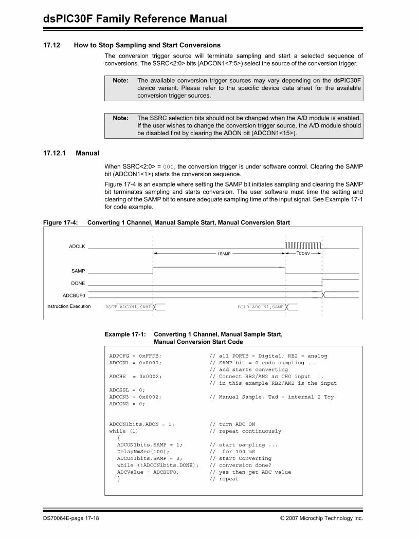
17.12 How to Stop Sampling and Start ConversionsThe conversion trigger source will terminate sampling and start a selected sequence ofconversions. The SSRC<2:0> bits (ADCON1<7:5>) select the source of the conversion trigger.
17.12.1 Manual
When SSRC<2:0> = 000, the conversion trigger is under software control. Clearing the SAMPbit (ADCON1<1>) starts the conversion sequence.
Figure 17-4 is an example where setting the SAMP bit initiates sampling and clearing the SAMPbit terminates sampling and starts conversion. The user software must time the setting andclearing of the SAMP bit to ensure adequate sampling time of the input signal. See Example 17-1for code example.
Figure 17-4: Converting 1 Channel, Manual Sample Start, Manual Conversion Start
Example 17-1: Converting 1 Channel, Manual Sample Start,Manual Conversion Start Code
Note: The available conversion trigger sources may vary depending on the dsPIC30Fdevice variant. Please refer to the specific device data sheet for the availableconversion trigger sources.
Note: The SSRC selection bits should not be changed when the A/D module is enabled.If the user wishes to change the conversion trigger source, the A/D module shouldbe disabled first by clearing the ADON bit (ADCON1<15>).
ADCLK
SAMP
ADCBUF0
TSAMP TCONV
BCLR ADCON1,SAMPBSET ADCON1,SAMPInstruction Execution
DONE
ADPCFG = 0xFFFB; // all PORTB = Digital; RB2 = analog ADCON1 = 0x0000; // SAMP bit = 0 ends sampling ...
// and starts converting ADCHS = 0x0002; // Connect RB2/AN2 as CH0 input ..
// in this example RB2/AN2 is the input ADCSSL = 0; ADCON3 = 0x0002; // Manual Sample, Tad = internal 2 Tcy ADCON2 = 0;
ADCON1bits.ADON = 1; // turn ADC ON while (1) // repeat continuously
{ ADCON1bits.SAMP = 1; // start sampling ... DelayNmSec(100); // for 100 mS ADCON1bits.SAMP = 0; // start Converting
while (!ADCON1bits.DONE); // conversion done? ADCValue = ADCBUF0; // yes then get ADC value
} // repeat
DS70064E-page 17-18 © 2007 Microchip Technology Inc.

Section 17. 10-bit A/D Converter10-bit A
/DC
onverter
17
Figure 17-5 is an example where setting the ASAM bit initiates automatic sampling and clearingthe SAMP bit terminates sampling and starts conversion. After the conversion completes, themodule will automatically return to a sampling state. The SAMP bit is automatically set at the startof the sample interval. The user software must time the clearing of the SAMP bit to ensureadequate sampling time of the input signal, understanding that the time between clearing of theSAMP bit includes the conversion time as well as the sampling time. See Example 17-2 for codeexample.
Figure 17-5: Converting 1 Channel, Automatic Sample Start, Manual Conversion Start
Example 17-2: Converting 1 Channel, Automatic Sample Start,Manual Conversion Start Code
ADCLK
SAMP
ADCBUF0
TSAMP TCONV
BCLR ADCON1,SAMP Instruction Execution
TCONV
BSET ADCON1,ASAM BCLR ADCON1,SAMP
TSAMPTAD0 TAD0
DONE
ADPCFG = 0xFF7F; // all PORTB = Digital but RB7 = analog ADCON1 = 0x0004; // ASAM bit = 1 implies sampling ..
// starts immediately after last // conversion is done
ADCHS = 0x0007; // Connect RB7/AN7 as CH0 input ..// in this example RB7/AN7 is the input
ADCSSL = 0; ADCON3 = 0x0002; // Sample time manual, Tad = internal 2 Tcy ADCON2 = 0;
ADCON1bits.ADON = 1; // turn ADC ON while (1) // repeat continuously
{ DelayNmSec(100); // sample for 100 mS ADCON1bits.SAMP = 0; // start Converting
while (!ADCON1bits.DONE); // conversion done? ADCValue = ADCBUF0; // yes then get ADC value
} // repeat
© 2007 Microchip Technology Inc. DS70064E-page 17-19
dsPIC30F Family Reference Manual
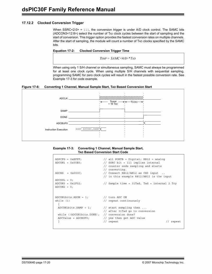
17.12.2 Clocked Conversion Trigger
When SSRC<2:0> = 111, the conversion trigger is under A/D clock control. The SAMC bits(ADCON3<12:8>) select the number of TAD clock cycles between the start of sampling and thestart of conversion. This trigger option provides the fastest conversion rates on multiple channels.After the start of sampling, the module will count a number of TAD clocks specified by the SAMCbits.
Equation 17-2: Clocked Conversion Trigger Time
When using only 1 S/H channel or simultaneous sampling, SAMC must always be programmedfor at least one clock cycle. When using multiple S/H channels with sequential sampling,programming SAMC for zero clock cycles will result in the fastest possible conversion rate. SeeExample 17-3 for code example.
Figure 17-6: Converting 1 Channel, Manual Sample Start, TAD Based Conversion Start
Example 17-3: Converting 1 Channel, Manual Sample Start,TAD Based Conversion Start Code
TSMP = SAMC<4:0>*TAD
ADCLK
SAMP
ADCBUF0
TSAMP TCONV
BSET ADCON1,SAMPInstruction Execution
DONE
= 16 TAD
ADPCFG = 0xEFFF; // all PORTB = Digital; RB12 = analog ADCON1 = 0x00E0; // SSRC bit = 111 implies internal
// counter ends sampling and starts// converting.
ADCHS = 0x000C; // Connect RB12/AN12 as CH0 input ..// in this example RB12/AN12 is the input
ADCSSL = 0; ADCON3 = 0x1F02; // Sample time = 31Tad, Tad = internal 2 Tcy ADCON2 = 0;
ADCON1bits.ADON = 1; // turn ADC ON while (1) // repeat continuously
{ ADCON1bits.SAMP = 1; // start sampling then ...
// after 31Tad go to conversionwhile (!ADCON1bits.DONE); // conversion done?
ADCValue = ADCBUF0; // yes then get ADC value} // repeat // repeat
DS70064E-page 17-20 © 2007 Microchip Technology Inc.
Section 17. 10-bit A/D Converter10-bit A
/DC
onverter
17
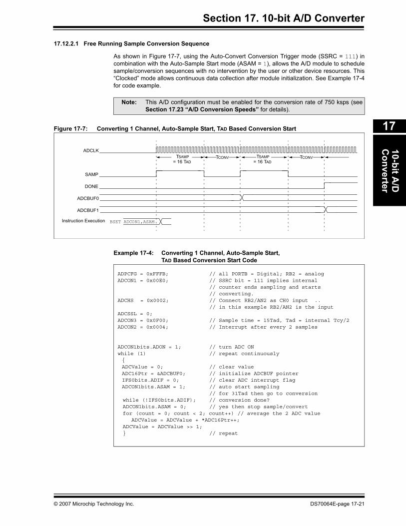
17.12.2.1 Free Running Sample Conversion Sequence
As shown in Figure 17-7, using the Auto-Convert Conversion Trigger mode (SSRC = 111) incombination with the Auto-Sample Start mode (ASAM = 1), allows the A/D module to schedulesample/conversion sequences with no intervention by the user or other device resources. This“Clocked” mode allows continuous data collection after module initialization. See Example 17-4for code example.
Figure 17-7: Converting 1 Channel, Auto-Sample Start, TAD Based Conversion Start
Example 17-4: Converting 1 Channel, Auto-Sample Start,TAD Based Conversion Start Code
Note: This A/D configuration must be enabled for the conversion rate of 750 ksps (seeSection 17.23 “A/D Conversion Speeds” for details).
ADCLK
SAMP
ADCBUF1
TSAMP TCONV
DONE
= 16 TADTSAMP TCONV
= 16 TAD
ADCBUF0
BSET ADCON1,ASAMInstruction Execution
ADPCFG = 0xFFFB; // all PORTB = Digital; RB2 = analog ADCON1 = 0x00E0; // SSRC bit = 111 implies internal
// counter ends sampling and starts// converting.
ADCHS = 0x0002; // Connect RB2/AN2 as CH0 input ..// in this example RB2/AN2 is the input
ADCSSL = 0; ADCON3 = 0x0F00; // Sample time = 15Tad, Tad = internal Tcy/2 ADCON2 = 0x0004; // Interrupt after every 2 samples
ADCON1bits.ADON = 1; // turn ADC ON while (1) // repeat continuously
{ADCValue = 0; // clear valueADC16Ptr = &ADCBUF0; // initialize ADCBUF pointerIFS0bits.ADIF = 0; // clear ADC interrupt flag
ADCON1bits.ASAM = 1; // auto start sampling // for 31Tad then go to conversion
while (!IFS0bits.ADIF); // conversion done?ADCON1bits.ASAM = 0; // yes then stop sample/convertfor (count = 0; count < 2; count++) // average the 2 ADC value
ADCValue = ADCValue + *ADC16Ptr++; ADCValue = ADCValue >> 1;} // repeat
© 2007 Microchip Technology Inc. DS70064E-page 17-21
dsPIC30F Family Reference Manual
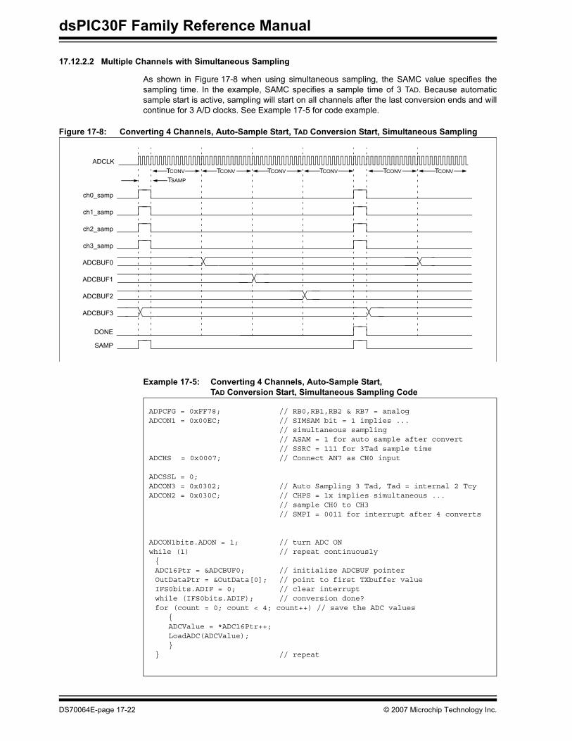
17.12.2.2 Multiple Channels with Simultaneous Sampling
As shown in Figure 17-8 when using simultaneous sampling, the SAMC value specifies thesampling time. In the example, SAMC specifies a sample time of 3 TAD. Because automaticsample start is active, sampling will start on all channels after the last conversion ends and willcontinue for 3 A/D clocks. See Example 17-5 for code example.
Figure 17-8: Converting 4 Channels, Auto-Sample Start, TAD Conversion Start, Simultaneous Sampling
Example 17-5: Converting 4 Channels, Auto-Sample Start,TAD Conversion Start, Simultaneous Sampling Code
TCONV TCONV TCONV TCONV
ADCLK
ch1_samp
ch2_samp
ch3_samp
ch0_samp
ADCBUF0
ADCBUF1
ADCBUF2
ADCBUF3
TCONV TCONV
DONE
SAMP
TSAMP
ADPCFG = 0xFF78; // RB0,RB1,RB2 & RB7 = analog ADCON1 = 0x00EC; // SIMSAM bit = 1 implies ...
// simultaneous sampling// ASAM = 1 for auto sample after convert// SSRC = 111 for 3Tad sample time
ADCHS = 0x0007; // Connect AN7 as CH0 input
ADCSSL = 0; ADCON3 = 0x0302; // Auto Sampling 3 Tad, Tad = internal 2 Tcy ADCON2 = 0x030C; // CHPS = 1x implies simultaneous ...
// sample CH0 to CH3// SMPI = 0011 for interrupt after 4 converts
ADCON1bits.ADON = 1; // turn ADC ON while (1) // repeat continuously
{ADC16Ptr = &ADCBUF0; // initialize ADCBUF pointerOutDataPtr = &OutData[0]; // point to first TXbuffer valueIFS0bits.ADIF = 0; // clear interruptwhile (IFS0bits.ADIF); // conversion done?for (count = 0; count < 4; count++) // save the ADC values
{ADCValue = *ADC16Ptr++;LoadADC(ADCValue);}
} // repeat
DS70064E-page 17-22 © 2007 Microchip Technology Inc.

Section 17. 10-bit A/D Converter10-bit A
/DC
onverter
17
17.12.2.3 Multiple Channels with Sequential Sampling
As shown in Figure 17-9 when using sequential sampling, the sample time precedes eachconversion time. In the example, 3 TAD clocks are added for sample time for each channel.
Figure 17-9: Converting 4 Channels, Auto-Sample Start, TAD Conversion Start, Sequential Sampling
17.12.2.4 Sample Time Considerations Using Clocked Conversion Trigger and Automatic Sampling
Different sample/conversion sequences provide different available sampling times for the S/Hchannel to acquire the analog signal. The user must ensure the sampling time exceeds thesampling requirements, as outlined in Section 17.17 “A/D Sampling Requirements”.
Assuming that the module is set for automatic sampling and using a clocked conversion trigger,the sampling interval is determined by the sample interval specified by the SAMC bits.
If the SIMSAM bit specifies simultaneous sampling or only one channel is active, the samplingtime is the period specified by the SAMC bit.
Equation 17-3: Available Sampling Time, Simultaneous Sampling
If the SIMSAM bit specifies sequential sampling, the total interval used to convert all channels isthe number of channels times the sampling time and conversion time. The sampling time for anindividual channel is the total interval minus the conversion time for that channel.
Equation 17-4: Available Sampling Time, Simultaneous Sampling
Note: This A/D configuration must be enabled for the configuration rates of 1 Msps and600 ksps (see Section 17.23 “A/D Conversion Speeds” for further details).
TCONV
ADCLK
ch1_samp
ch2_samp
ch3_samp
ch0_samp
ADRES(0)
ADRES(1)
ADRES(2)
ADRES(3)
TCONV TCONV TCONV TCONV
SAMP
TSAMP TSAMP
DONE = 0
TSEQ = Channels per Sample (CH/S) * ((SAMC<4:0> * TAD) + Conversion Time (TCONV))
TSMP = (TSEQ – TCONV)
Note 1: CH/S specified by CHPS<1:0> bits.2: TSEQ is the total time for the sample/convert sequence.
TSMP = SAMC<4:0> * TAD
© 2007 Microchip Technology Inc. DS70064E-page 17-23
dsPIC30F Family Reference Manual
17.12.3 Event Trigger Conversion Start
It is often desirable to synchronize the end of sampling and the start of conversion with someother time event. The A/D module may use one of three sources as a conversion trigger.
17.12.3.1 External INT Pin Trigger
When SSRC<2:0> = 001, the A/D conversion is triggered by an active transition on the INT0 pin.The INT0 pin may be programmed for either a rising edge input or a falling edge input.
17.12.3.2 GP Timer Compare Trigger
The A/D is configured in this Trigger mode by setting SSRC<2:0> = 010. When a match occursbetween the 32-bit timer TMR3/TMR2 and the 32-bit Combined Period register PR3/PR2, aspecial ADC trigger event signal is generated by Timer3. This feature does not exist for theTMR5/TMR4 timer pair. Refer to Section 12. “Timers” for more details.
17.12.3.3 Motor Control PWM Trigger
The PWM module has an event trigger that allows A/D conversions to be synchronized to thePWM time base. When SSRC<2:0> = 011, the A/D sampling and conversion times occur at anyuser programmable point within the PWM period. The special event trigger allows the user tominimize the delay between the time when A/D conversion results are acquired and the timewhen the duty cycle value is updated. Refer to Section 15. “Motor Control PWM” for moredetails.
17.12.3.4 Synchronizing A/D Operations to Internal or External Events
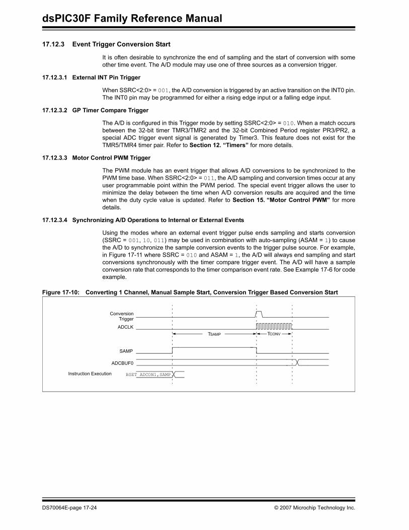
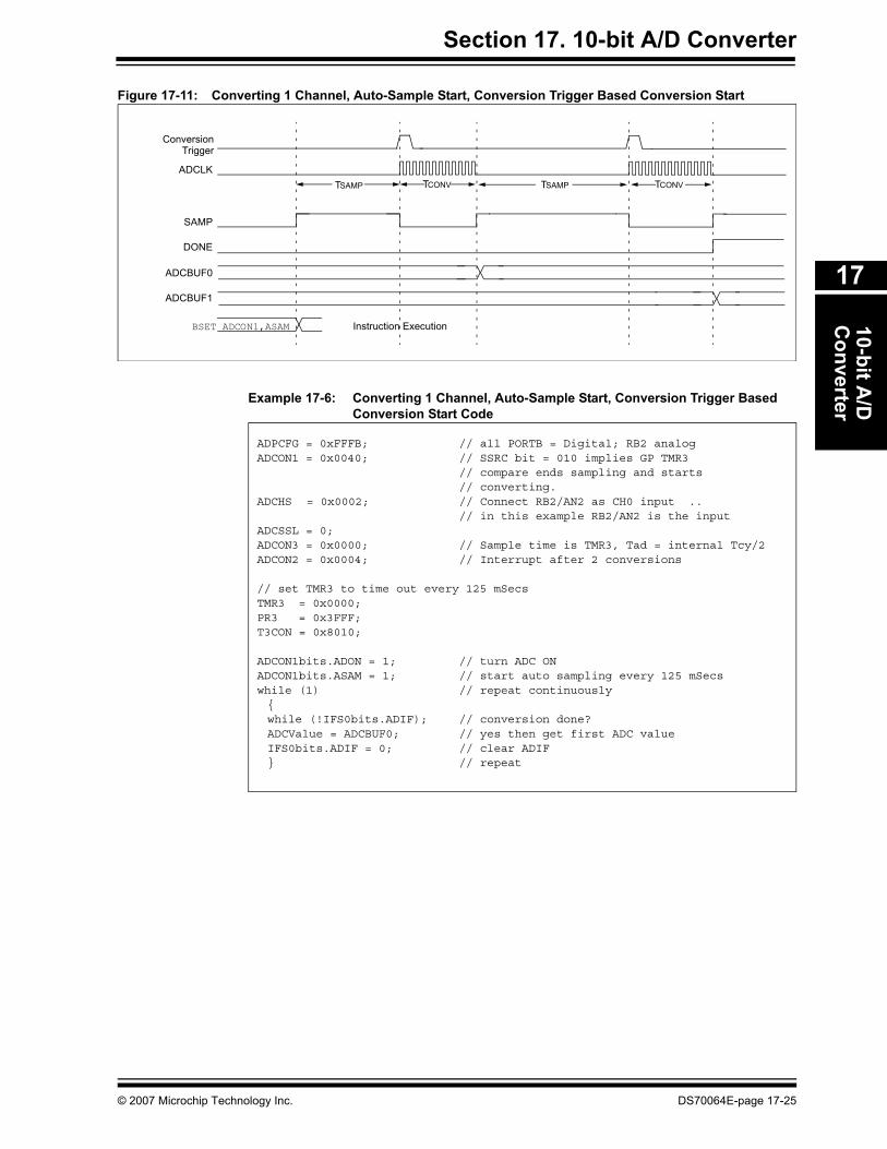
Using the modes where an external event trigger pulse ends sampling and starts conversion(SSRC = 001, 10, 011) may be used in combination with auto-sampling (ASAM = 1) to causethe A/D to synchronize the sample conversion events to the trigger pulse source. For example,in Figure 17-11 where SSRC = 010 and ASAM = 1, the A/D will always end sampling and startconversions synchronously with the timer compare trigger event. The A/D will have a sampleconversion rate that corresponds to the timer comparison event rate. See Example 17-6 for codeexample.
Figure 17-10: Converting 1 Channel, Manual Sample Start, Conversion Trigger Based Conversion Start
Conversion
ADCLK
SAMP
ADCBUF0
TSAMP TCONV
BSET ADCON1,SAMPInstruction Execution
Trigger
DS70064E-page 17-24 © 2007 Microchip Technology Inc.
Section 17. 10-bit A/D Converter10-bit A
/DC
onverter
17
Figure 17-11: Converting 1 Channel, Auto-Sample Start, Conversion Trigger Based Conversion Start
Example 17-6: Converting 1 Channel, Auto-Sample Start, Conversion Trigger Based Conversion Start Code
ADCLK
SAMP
ADCBUF0
TSAMP TCONV
BSET ADCON1,ASAM Instruction Execution
TCONVTSAMP
ADCBUF1
DONE
ConversionTrigger
ADPCFG = 0xFFFB; // all PORTB = Digital; RB2 analog ADCON1 = 0x0040; // SSRC bit = 010 implies GP TMR3
// compare ends sampling and starts// converting.
ADCHS = 0x0002; // Connect RB2/AN2 as CH0 input ..// in this example RB2/AN2 is the input
ADCSSL = 0; ADCON3 = 0x0000; // Sample time is TMR3, Tad = internal Tcy/2 ADCON2 = 0x0004; // Interrupt after 2 conversions
// set TMR3 to time out every 125 mSecs TMR3 = 0x0000; PR3 = 0x3FFF; T3CON = 0x8010; ADCON1bits.ADON = 1; // turn ADC ON ADCON1bits.ASAM = 1; // start auto sampling every 125 mSecs while (1) // repeat continuously
{ while (!IFS0bits.ADIF); // conversion done?
ADCValue = ADCBUF0; // yes then get first ADC valueIFS0bits.ADIF = 0; // clear ADIF} // repeat
© 2007 Microchip Technology Inc. DS70064E-page 17-25
dsPIC30F Family Reference Manual
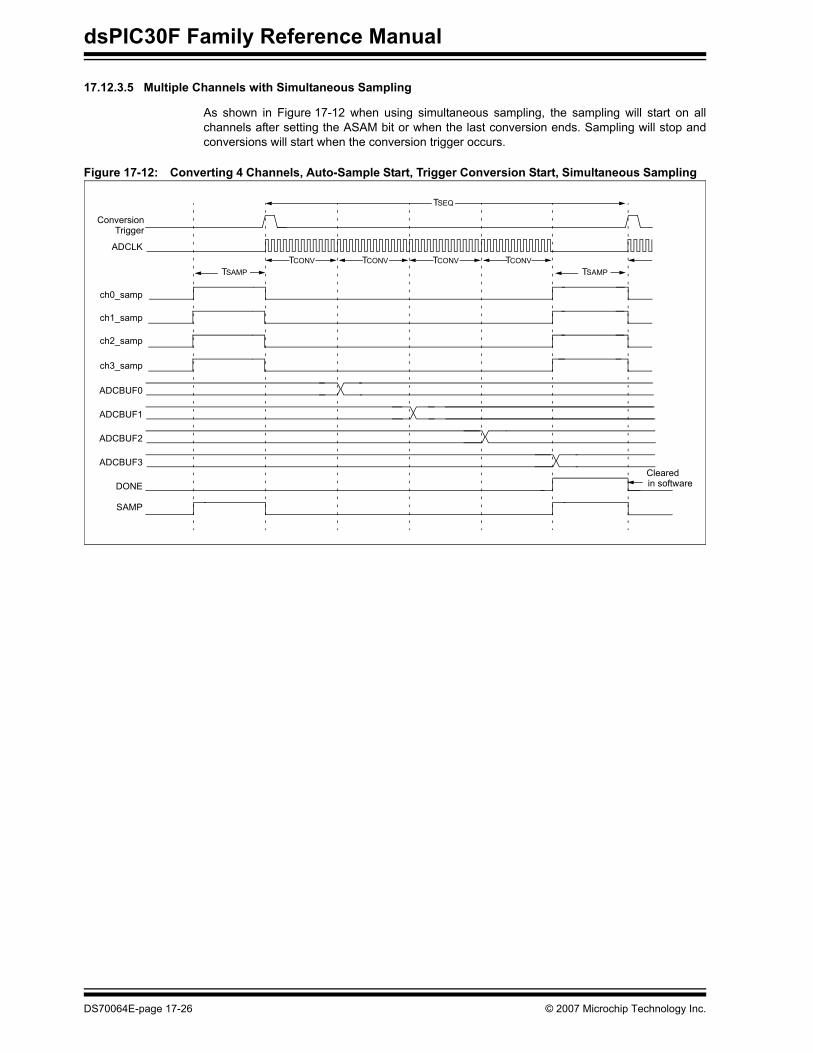
17.12.3.5 Multiple Channels with Simultaneous Sampling
As shown in Figure 17-12 when using simultaneous sampling, the sampling will start on allchannels after setting the ASAM bit or when the last conversion ends. Sampling will stop andconversions will start when the conversion trigger occurs.
Figure 17-12: Converting 4 Channels, Auto-Sample Start, Trigger Conversion Start, Simultaneous Sampling
TCONV TCONV TCONV TCONV
ADCLK
ch1_samp
ch2_samp
ch3_samp
ch0_samp
ADCBUF0
ADCBUF1
ADCBUF2
ADCBUF3
DONE
TSAMP
SAMP
TSAMP
TSEQ
ConversionTrigger
Clearedin software
DS70064E-page 17-26 © 2007 Microchip Technology Inc.
Section 17. 10-bit A/D Converter10-bit A
/DC
onverter
17
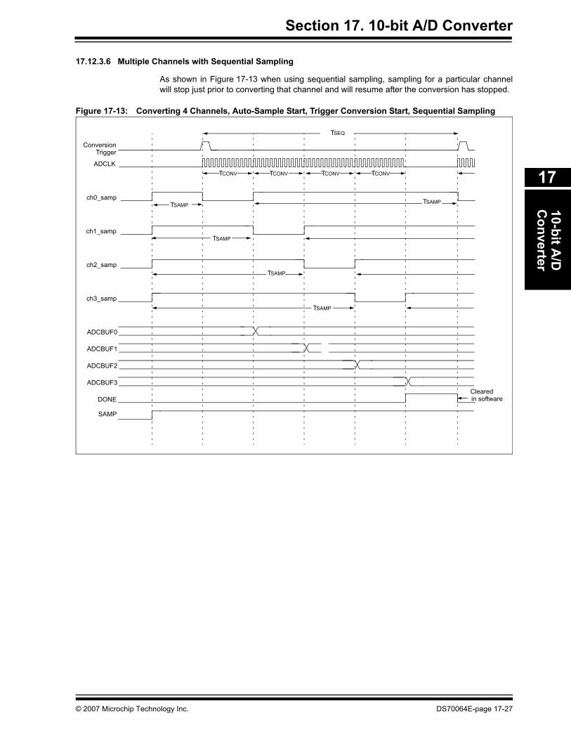
17.12.3.6 Multiple Channels with Sequential Sampling
As shown in Figure 17-13 when using sequential sampling, sampling for a particular channelwill stop just prior to converting that channel and will resume after the conversion has stopped.
Figure 17-13: Converting 4 Channels, Auto-Sample Start, Trigger Conversion Start, Sequential Sampling
TCONV TCONV TCONV TCONV
ADCLK
ch1_samp
ch2_samp
ch3_samp
ch0_samp
ADCBUF0
ADCBUF1
ADCBUF2
ADCBUF3
DONE
TSAMP
TSAMP
TSAMP
TSAMP
SAMP
TSAMP
TSEQ
ConversionTrigger
Clearedin software
© 2007 Microchip Technology Inc. DS70064E-page 17-27
dsPIC30F Family Reference Manual
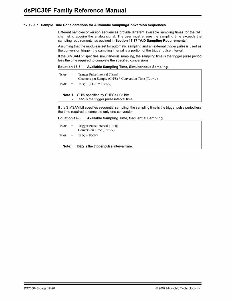
17.12.3.7 Sample Time Considerations for Automatic Sampling/Conversion Sequences
Different sample/conversion sequences provide different available sampling times for the S/Hchannel to acquire the analog signal. The user must ensure the sampling time exceeds thesampling requirements, as outlined in Section 17.17 “A/D Sampling Requirements”.
Assuming that the module is set for automatic sampling and an external trigger pulse is used asthe conversion trigger, the sampling interval is a portion of the trigger pulse interval.
If the SIMSAM bit specifies simultaneous sampling, the sampling time is the trigger pulse periodless the time required to complete the specified conversions.
Equation 17-5: Available Sampling Time, Simultaneous Sampling
If the SIMSAM bit specifies sequential sampling, the sampling time is the trigger pulse period lessthe time required to complete only one conversion.
Equation 17-6: Available Sampling Time, Sequential Sampling
TSMP = Trigger Pulse Interval (TSEQ) –Channels per Sample (CH/S) * Conversion Time (TCONV)
TSMP = TSEQ – (CH/S * TCONV)
Note 1: CH/S specified by CHPS<1:0> bits.2: TSEQ is the trigger pulse interval time.
TSMP = Trigger Pulse Interval (TSEQ) –Conversion Time (TCONV)
TSMP = TSEQ – TCONV
Note: TSEQ is the trigger pulse interval time.
DS70064E-page 17-28 © 2007 Microchip Technology Inc.

Section 17. 10-bit A/D Converter10-bit A
/DC
onverter
17
17.13 Controlling Sample/Conversion OperationThe application software may poll the SAMP and DONE bits to keep track of the A/D operationsor the module can interrupt the CPU when conversions are complete. The application softwaremay also abort A/D operations if necessary.
17.13.1 Monitoring Sample/Conversion Status
The SAMP (ADCON1<1>) and DONE (ADCON1<0>) bits indicate the sampling state and theconversion state of the A/D, respectively. Generally, when the SAMP bit clears, indicating end ofsampling, the DONE bit is automatically set, indicating end of conversion. If both SAMP andDONE are ‘0’, the A/D is in an inactive state. In some Operational modes, the SAMP bit may alsoinvoke and terminate sampling.
17.13.2 Generating an A/D Interrupt
The SMPI<3:0> bits control the generation of interrupts. The interrupt will occur some number ofsample/conversion sequences after starting sampling and re-occur on each equivalent numberof samples. Note that the interrupts are specified in terms of samples and not in terms ofconversions or data samples in the buffer memory.
When the SIMSAM bit specifies sequential sampling, regardless of the number of channelsspecified by the CHPS bits, the module samples once for each conversion and data sample inthe buffer. Therefore, the value specified by the SMPI bits will correspond to the number of datasamples in the buffer, up to the maximum of 16.
When the SIMSAM bit specifies simultaneous sampling, the number of data samples in the bufferis related to the CHPS bits. Algorithmically, the channels/sample times the number of sampleswill result in the number of data sample entries in the buffer. To avoid loss of data in the bufferdue to overruns, the SMPI bits must be set to the desired buffer size divided by the channels persample.
Disabling the A/D interrupt is not done with the SMPI bits. To disable the interrupt, clear the ADIEanalog module interrupt enable bit.
17.13.3 Aborting Sampling
Clearing the SAMP bit while in Manual Sampling mode will terminate sampling, but may also starta conversion if SSRC = 000.
Clearing the ASAM bit while in Automatic Sampling mode will not terminate an on goingsample/convert sequence, however, sampling will not automatically resume after subsequentconversions.
17.13.4 Aborting a Conversion
Clearing the ADON bit during a conversion will abort the current conversion. The A/D Resultregister pair will NOT be updated with the partially completed A/D conversion sample. That is,the corresponding ADCBUF buffer location will continue to contain the value of the lastcompleted conversion (or the last value written to the buffer).
© 2007 Microchip Technology Inc. DS70064E-page 17-29
dsPIC30F Family Reference Manual
17.14 Specifying How Conversion Results are Written Into the BufferAs conversions are completed, the module writes the results of the conversions into the A/Dresult buffer. This buffer is a RAM array of sixteen 10-bit words. The buffer is accessed through16 address locations within the SFR space named ADCBUF0...ADCBUFF.
User software may attempt to read each A/D conversion result as it is generated, however, thiswould consume too much CPU time. Generally, to simplify the code, the module will fill the bufferwith results and then generate an interrupt when the buffer is filled.
17.14.1 Number of Conversions per Interrupt
The SMPI<3:0> bits (ADCON2<5:2>) will select how many A/D conversions will take placebefore the CPU is interrupted. This can vary from 1 sample per interrupt to 16 samples perinterrupt. The A/D converter module always starts writing its conversion results at the beginningof the buffer, after each interrupt. For example, if SMPI<3:0> = 0000, the conversion results willalways be written to ADCBUF0. In this example, no other buffer locations would be used.
17.14.2 Restrictions Due to Buffer Size
The user cannot program a combination of CHPS and SMPI bits that specifies more than 16conversions per interrupt when the BUFM bit (ADCON2<1>) is ‘0’, or 8 conversions per interruptwhen the BUFM bit (ADCON2<1>) is ‘0’. The BUFM bit function is described below.
17.14.3 Buffer Fill Mode
When the BUFM bit (ADCON2<1>) is ‘1’, the 16-word results buffer (ADRES) will be split into two8-word groups. The 8-word buffers will alternately receive the conversion results after eachinterrupt event. The initial 8-word buffer used after BUFM is set will be located at the loweraddresses of ADCBUF. When BUFM is ‘0’, the complete 16-word buffer is used for all conversionsequences.
The decision to use the BUFM feature will depend upon how much time is available to move thebuffer contents after the interrupt, as determined by the application. If the processor can quicklyunload a full buffer within the time it takes to sample and convert one channel, the BUFM bit canbe ‘0’ and up to 16 conversions may be done per interrupt. The processor will have one sampleand conversion time before the first buffer location is overwritten.
If the processor cannot unload the buffer within the sample and conversion time, the BUFM bitshould be ‘1’. For example, if SMPI<3:0> = 0111, then eight conversions will be loaded into 1/2of the buffer, following which an interrupt will occur. The next eight conversions will be loaded intothe other 1/2 of the buffer. The processor will therefore have the entire time between interruptsto move the eight conversions out of the buffer.
17.14.4 Buffer Fill Status
When the conversion result buffer is split using the BUFM control bit, the BUFS status bit(ADCON2<7>) indicates the half of the buffer that the A/D converter is currently filling. IfBUFS = 0, then the A/D converter is filling ADCBUF0-ADCBUF7 and the user software shouldread conversion values from ADCBUF8-ADCBUFF. If BUFS = 1, the situation is reversed andthe user software should read conversion values from ADCBUF0-ADCBUF7.
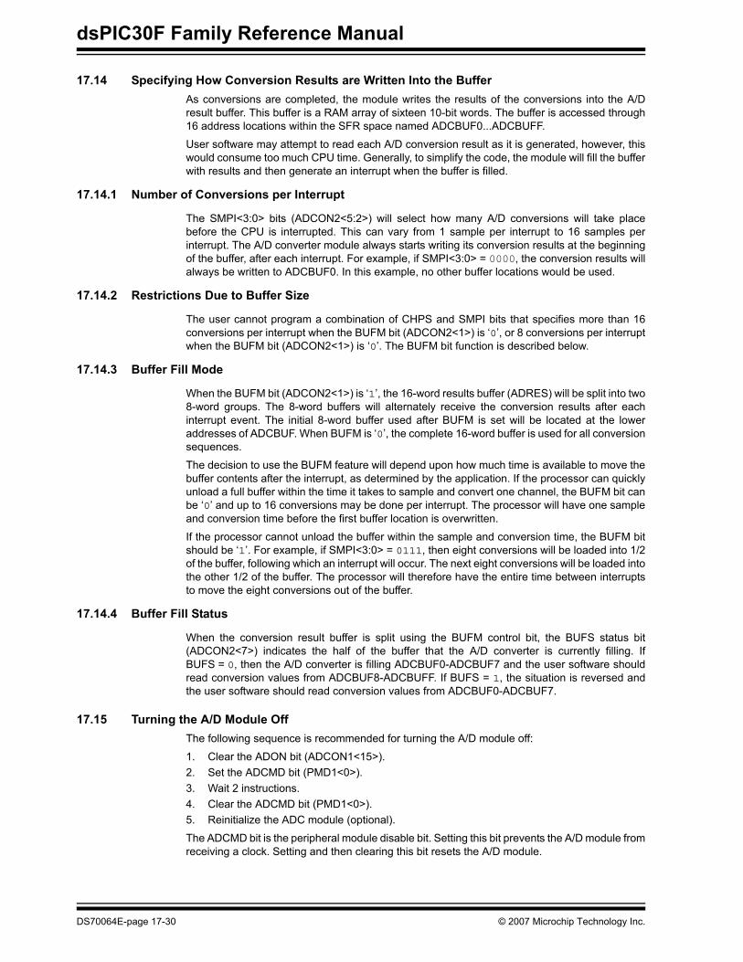
17.15 Turning the A/D Module OffThe following sequence is recommended for turning the A/D module off:
1. Clear the ADON bit (ADCON1<15>).2. Set the ADCMD bit (PMD1<0>).3. Wait 2 instructions.4. Clear the ADCMD bit (PMD1<0>).5. Reinitialize the ADC module (optional).
The ADCMD bit is the peripheral module disable bit. Setting this bit prevents the A/D module fromreceiving a clock. Setting and then clearing this bit resets the A/D module.
DS70064E-page 17-30 © 2007 Microchip Technology Inc.

Section 17. 10-bit A/D Converter10-bit A
/DC
onverter
17
17.16 Conversion Sequence ExamplesThe following configuration examples show the A/D operation in different sampling and bufferingconfigurations. In each example, setting the ASAM bit starts automatic sampling. A conversiontrigger ends sampling and starts conversion.
17.16.1 Example: Sampling and Converting a Single Channel Multiple Times
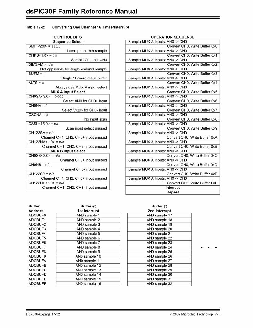
Figure 17-11 and Table 17-2 illustrate a basic configuration of the A/D. In this case, one A/Dinput, AN0, will be sampled by one sample and hold channel, CH0, and converted. The resultsare stored in the ADCBUF buffer. This process repeats 16 times until the buffer is full and thenthe module generates an interrupt. The entire process will then repeat.
The CHPS bits specify that only sample/hold CH0 is active. With ALTS clear, only the MUX Ainputs are active. The CH0SA bits and CH0NA bit are specified (AN0-VREF-) as the input to thesample/hold channel. All other input selection bits are not used.
Figure 17-14: Converting One Channel 16 Times/Interrupt
ADCLK
SAMP
ADCBUF0
TSAMP
TCONV
BSET ADCON1,ASAM Instruction Execution
ADCBUF1
DONE
ADCBUFE
ADCBUFF
Input to CH0 AN0
TSAMP
TCONV
AN0
TSAMP
TCONV
AN0
TSAMP
TCONV
AN0
ADIF
ASAM
ConversionTrigger
© 2007 Microchip Technology Inc. DS70064E-page 17-31
dsPIC30F Family Reference Manual
Table 17-2: Converting One Channel 16 Times/Interrupt
CONTROL BITS OPERATION SEQUENCESequence Select Sample MUX A Inputs: AN0 -> CH0
SMPI<2:0> = 1111 Convert CH0, Write Buffer 0x0Interrupt on 16th sample Sample MUX A Inputs: AN0 -> CH0
CHPS<1:0> = 00 Convert CH0, Write Buffer 0x1Sample Channel CH0 Sample MUX A Inputs: AN0 -> CH0
SIMSAM = n/a Convert CH0, Write Buffer 0x2Not applicable for single channel sample Sample MUX A Inputs: AN0 -> CH0
BUFM = 0 Convert CH0, Write Buffer 0x3Single 16-word result buffer Sample MUX A Inputs: AN0 -> CH0
ALTS = 0 Convert CH0, Write Buffer 0x4Always use MUX A input select Sample MUX A Inputs: AN0 -> CH0
MUX A Input Select Convert CH0, Write Buffer 0x5CH0SA<3:0> = 0000 Sample MUX A Inputs: AN0 -> CH0
Select AN0 for CH0+ input Convert CH0, Write Buffer 0x6CH0NA = 0 Sample MUX A Inputs: AN0 -> CH0
Select VREF- for CH0- input Convert CH0, Write Buffer 0x7CSCNA = 0 Sample MUX A Inputs: AN0 -> CH0
No input scan Convert CH0, Write Buffer 0x8CSSL<15:0> = n/a Sample MUX A Inputs: AN0 -> CH0
Scan input select unused Convert CH0, Write Buffer 0x9CH123SA = n/a Sample MUX A Inputs: AN0 -> CH0
Channel CH1, CH2, CH3+ input unused Convert CH0, Write Buffer 0xACH123NA<1:0> = n/a Sample MUX A Inputs: AN0 -> CH0
Channel CH1, CH2, CH3- input unused Convert CH0, Write Buffer 0xBMUX B Input Select Sample MUX A Inputs: AN0 -> CH0
CH0SB<3:0> = n/a Convert CH0, Write Buffer 0xCChannel CH0+ input unused Sample MUX A Inputs: AN0 -> CH0
CH0NB = n/a Convert CH0, Write Buffer 0xDChannel CH0- input unused Sample MUX A Inputs: AN0 -> CH0
CH123SB = n/a Convert CH0, Write Buffer 0xEChannel CH1, CH2, CH3+ input unused Sample MUX A Inputs: AN0 -> CH0
CH123NB<1:0> = n/a Convert CH0, Write Buffer 0xFChannel CH1, CH2, CH3- input unused Interrupt
Repeat
BufferAddress
Buffer @1st Interrupt
Buffer @2nd Interrupt
ADCBUF0 AN0 sample 1 AN0 sample 17ADCBUF1 AN0 sample 2 AN0 sample 18ADCBUF2 AN0 sample 3 AN0 sample 19ADCBUF3 AN0 sample 4 AN0 sample 20ADCBUF4 AN0 sample 5 AN0 sample 21ADCBUF5 AN0 sample 6 AN0 sample 22ADCBUF6 AN0 sample 7 AN0 sample 23ADCBUF7 AN0 sample 8 AN0 sample 24 • • •ADCBUF8 AN0 sample 9 AN0 sample 25ADCBUF9 AN0 sample 10 AN0 sample 26ADCBUFA AN0 sample 11 AN0 sample 27ADCBUFB AN0 sample 12 AN0 sample 28ADCBUFC AN0 sample 13 AN0 sample 29ADCBUFD AN0 sample 14 AN0 sample 30ADCBUFE AN0 sample 15 AN0 sample 31ADCBUFF AN0 sample 16 AN0 sample 32
DS70064E-page 17-32 © 2007 Microchip Technology Inc.
Section 17. 10-bit A/D Converter10-bit A
/DC
onverter
17
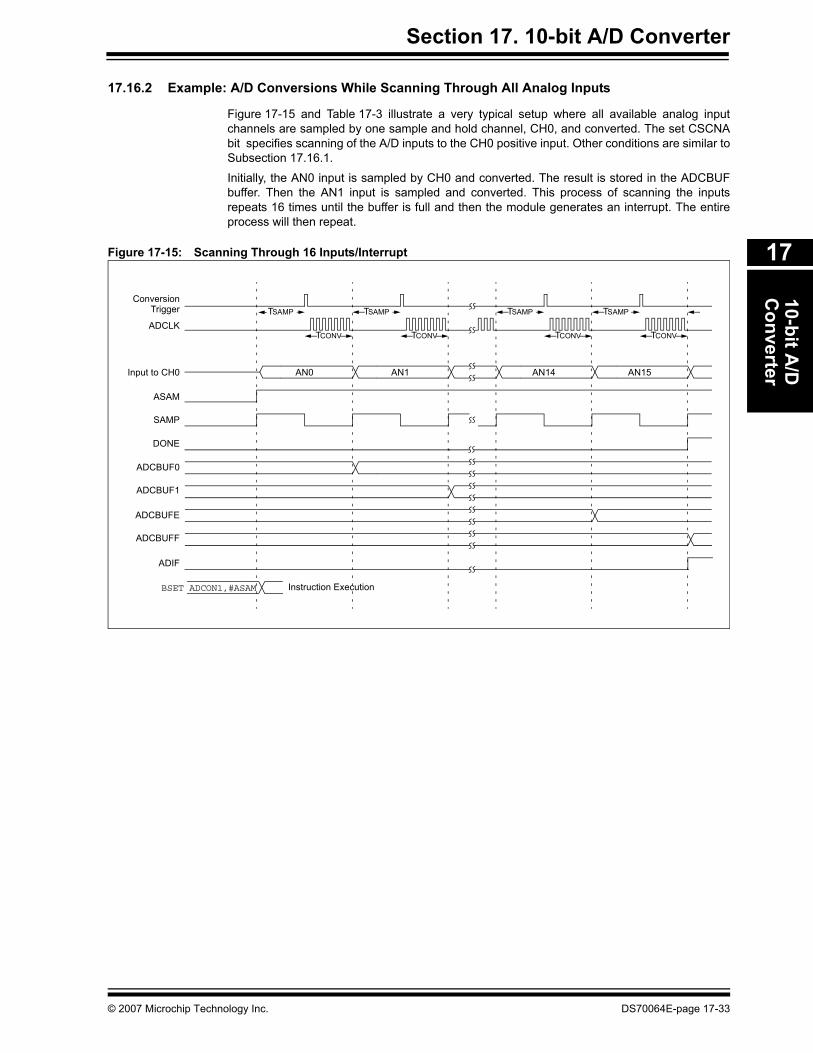
17.16.2 Example: A/D Conversions While Scanning Through All Analog Inputs
Figure 17-15 and Table 17-3 illustrate a very typical setup where all available analog inputchannels are sampled by one sample and hold channel, CH0, and converted. The set CSCNAbit specifies scanning of the A/D inputs to the CH0 positive input. Other conditions are similar toSubsection 17.16.1.
Initially, the AN0 input is sampled by CH0 and converted. The result is stored in the ADCBUFbuffer. Then the AN1 input is sampled and converted. This process of scanning the inputsrepeats 16 times until the buffer is full and then the module generates an interrupt. The entireprocess will then repeat.
Figure 17-15: Scanning Through 16 Inputs/Interrupt
ADCLK
SAMP
ADCBUF0
TSAMP
TCONV
BSET ADCON1,#ASAM Instruction Execution
ADCBUF1
DONE
ADCBUFE
ADCBUFF
Input to CH0 AN0
TSAMP
TCONV
AN1
TSAMP
TCONV
AN14
TSAMP
TCONV
AN15
ADIF
ASAM
ConversionTrigger
© 2007 Microchip Technology Inc. DS70064E-page 17-33

dsPIC30F Family Reference Manual
Table 17-3: Scanning Through 16 Inputs/Interrupt
CONTROL BITS OPERATION SEQUENCESequence Select Sample MUX A Inputs: AN0 -> CH0
SMPI<2:0> = 1111 Convert CH0, Write Buffer 0x0Interrupt on 16th sample Sample MUX A Inputs: AN1 -> CH0
CHPS<1:0> = 00 Convert CH0, Write Buffer 0x1Sample Channel CH0 Sample MUX A Inputs: AN2 -> CH0
SIMSAM = n/a Convert CH0, Write Buffer 0x2Not applicable for single channel sample Sample MUX A Inputs: AN3 -> CH0
BUFM = 0 Convert CH0, Write Buffer 0x3Single 16-word result buffer Sample MUX A Inputs: AN4 -> CH0
ALTS = 0 Convert CH0, Write Buffer 0x4Always use MUX A input select Sample MUX A Inputs: AN5 -> CH0
MUX A Input Select Convert CH0, Write Buffer 0x5CH0SA<3:0> = n/a Sample MUX A Inputs: AN6 -> CH0
Override by CSCNA Convert CH0, Write Buffer 0x6CH0NA = 0 Sample MUX A Inputs: AN7 -> CH0
Select VREF- for CH0- input Convert CH0, Write Buffer 0x7CSCNA = 1 Sample MUX A Inputs: AN8 -> CH0
Scan CH0+ Inputs Convert CH0, Write Buffer 0x8CSSL<15:0> = 1111 1111 1111 1111 Sample MUX A Inputs: AN9 -> CH0
Scan input select unused Convert CH0, Write Buffer 0x9CH123SA = n/a Sample MUX A Inputs: AN10 -> CH0
Channel CH1, CH2, CH3+ input unused Convert CH0, Write Buffer 0xACH123NA<1:0> = n/a Sample MUX A Inputs: AN11 -> CH0
Channel CH1, CH2, CH3- input unused Convert CH0, Write Buffer 0xBMUX B Input Select Sample MUX A Inputs: AN12 -> CH0
CH0SB<3:0> = n/a Convert CH0, Write Buffer 0xCChannel CH0+ input unused Sample MUX A Inputs: AN13 -> CH0
CH0NB = n/a Convert CH0, Write Buffer 0xDChannel CH0- input unused Sample MUX A Inputs: AN14 -> CH0
CH123SB = n/a Convert CH0, Write Buffer 0xEChannel CH1, CH2, CH3+ input unused Sample MUX A Inputs: AN15 -> CH0
CH123NB<1:0> = n/a Convert CH0, Write Buffer 0xFChannel CH1, CH2, CH3- input unused Interrupt
Repeat
BufferAddress
Buffer @1st Interrupt
Buffer @2nd Interrupt
ADCBUF0 AN0 sample 1 AN0 sample 17ADCBUF1 AN1 sample 2 AN1 sample 18ADCBUF2 AN2 sample 3 AN2 sample 19ADCBUF3 AN3 sample 4 AN3 sample 20ADCBUF4 AN4 sample 5 AN4 sample 21ADCBUF5 AN5 sample 6 AN5 sample 22ADCBUF6 AN6 sample 7 AN6 sample 23ADCBUF7 AN7 sample 8 AN7 sample 24 • • •ADCBUF8 AN8 sample 9 AN8 sample 25ADCBUF9 AN9 sample 10 AN9 sample 26ADCBUFA AN10 sample 11 AN10 sample 27ADCBUFB AN11 sample 12 AN11 sample 28ADCBUFC AN12 sample 13 AN12 sample 29ADCBUFD AN13 sample 14 AN13 sample 30ADCBUFE AN14 sample 15 AN14 sample 31ADCBUFF AN15 sample 16 AN15 sample 32
DS70064E-page 17-34 © 2007 Microchip Technology Inc.

Section 17. 10-bit A/D Converter10-bit A
/DC
onverter
17
17.16.3 Example: Sampling Three Inputs Frequently While Scanning Four Other Inputs
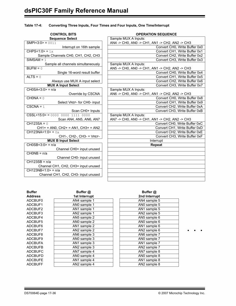
Figure 17-16 and Table 17-4 shows how the A/D converter could be configured to sample threeinputs frequently using sample/hold channels CH1, CH2 and CH3; while four other inputs aresampled less frequently by scanning them using sample/hold channel CH0. In this case, onlyMUX A inputs are used, and all 4 channels are sampled simultaneously. Four different inputs(AN4, AN5, AN6, AN7) are scanned in CH0, whereas AN0, AN1 and AN2 are the fixed inputs forCH1, CH2 and CH3, respectively. Thus, in every set of 16 samples, AN0, AN1 and AN2 wouldbe sampled 4 times, while AN4, AN5, AN6 and AN7 would be sampled only once each.
Figure 17-16: Converting Three Inputs, Four Times and Four Inputs, One Time/Interrupt
ADCLK
SAMP
DONE
Input to CH0 AN4
TSAMP
ADIF
TCONVTCONVTCONVTCONV
AN0
AN1
AN2
Input to CH1
Input to CH2
Input to CH3
ADCBUFD
ADCBUFE
ADCBUFF
AN5
TSAMP
AN0
AN1
AN2
AN7
TSAMP
AN0
AN1
AN2
ASAM
AN4
AN0
AN1
AN2
ADCBUF0
ADCBUF1
ADCBUF2
ADCBUF3
ADCBUFC
AN6
AN0
AN1
AN2
ConversionTrigger
TCONVTCONVTCONVTCONV TCONVTCONVTCONVTCONV
© 2007 Microchip Technology Inc. DS70064E-page 17-35
dsPIC30F Family Reference Manual
Table 17-4: Converting Three Inputs, Four Times and Four Inputs, One Time/Interrupt
CONTROL BITS OPERATION SEQUENCESequence Select Sample MUX A Inputs:
SMPI<3:0> = 0011 AN4 -> CH0, AN0 -> CH1, AN1 -> CH2, AN2 -> CH3Interrupt on 16th sample Convert CH0, Write Buffer 0x0
CHPS<1:0> = 1x Convert CH1, Write Buffer 0x1Sample Channels CH0, CH1, CH2, CH3 Convert CH2, Write Buffer 0x2
SIMSAM = 1 Convert CH3, Write Buffer 0x3Sample all channels simultaneously Sample MUX A Inputs:
BUFM = 0 AN5 -> CH0, AN0 -> CH1, AN1 -> CH2, AN2 -> CH3Single 16-word result buffer Convert CH0, Write Buffer 0x4
ALTS = 0 Convert CH1, Write Buffer 0x5Always use MUX A input select Convert CH2, Write Buffer 0x6
MUX A Input Select Convert CH3, Write Buffer 0x7CH0SA<3:0> = n/a Sample MUX A Inputs:
Override by CSCNA AN6 -> CH0, AN0 -> CH1, AN1 -> CH2, AN2 -> CH3CH0NA = 0 Convert CH0, Write Buffer 0x8
Select VREF- for CH0- input Convert CH1, Write Buffer 0x9CSCNA = 1 Convert CH2, Write Buffer 0xA
Scan CH0+ Inputs Convert CH3, Write Buffer 0xBCSSL<15:0> = 0000 0000 1111 0000 Sample MUX A Inputs:
Scan AN4, AN5, AN6, AN7 AN7 -> CH0, AN0 -> CH1, AN1 -> CH2, AN2 -> CH3CH123SA = 0 Convert CH0, Write Buffer 0xC
CH1+ = AN0, CH2+ = AN1, CH3+ = AN2 Convert CH1, Write Buffer 0xDCH123NA<1:0> = 0x Convert CH2, Write Buffer 0xE
CH1-, CH2-, CH3- = VREF- Convert CH3, Write Buffer 0xFMUX B Input Select Interrupt
CH0SB<3:0> = n/a RepeatChannel CH0+ input unused
CH0NB = n/aChannel CH0- input unused
CH123SB = n/aChannel CH1, CH2, CH3+ input unused
CH123NB<1:0> = n/aChannel CH1, CH2, CH3- input unused
BufferAddress
Buffer @1st Interrupt
Buffer @2nd Interrupt
ADCBUF0 AN4 sample 1 AN4 sample 5ADCBUF1 AN0 sample 1 AN0 sample 5ADCBUF2 AN1 sample 1 AN1 sample 5ADCBUF3 AN2 sample 1 AN2 sample 5ADCBUF4 AN5 sample 2 AN5 sample 6ADCBUF5 AN0 sample 2 AN0 sample 6ADCBUF6 AN1 sample 2 AN1 sample 6ADCBUF7 AN2 sample 2 AN2 sample 6 • • •ADCBUF8 AN6 sample 3 AN6 sample 7ADCBUF9 AN0 sample 3 AN0 sample 7ADCBUFA AN1 sample 3 AN1 sample 7ADCBUFB AN2 sample 3 AN2 sample 7ADCBUFC AN7 sample 4 AN7 sample 8ADCBUFD AN0 sample 4 AN0 sample 8ADCBUFE AN1 sample 4 AN1 sample 8ADCBUFF AN2 sample 4 AN2 sample 8
DS70064E-page 17-36 © 2007 Microchip Technology Inc.

Section 17. 10-bit A/D Converter10-bit A
/DC
onverter
17
17.16.4 Example: Using Dual 8-Word Buffers
Figure 17-17 and Table 17-5 demonstrate using dual 8-word buffers and alternating the buffer fill.Setting the BUFM bit enables dual 8-word buffers. The BUFM setting does not affect otheroperational parameters. First, the conversion sequence starts filling the buffer at ADCBUF0(buffer location 0x0). After the first interrupt occurs, the buffer begins to fill at ADCBUF8 (bufferlocation 0x8). The BUFS status bit is set and cleared alternately after each interrupt. In thisexample, all four channels are sampled simultaneously, and an interrupt occurs after everysample.
Figure 17-17: Converting Four Inputs, One Time/Interrupt Using Dual 8-Word Buffers
ADCLK
SAMP
ADCBUF0
BSET ADCON1,#ASAM Instruction Execution
ADCBUF1
ADCBUF2
ADCBUF3
Input to CH0 AN3
TSAMP
ADIF
AN0
AN1
AN2
Input to CH1
Input to CH2
Input to CH3
ADCBUF8
ADCBUF9
ADCBUFA
ADCBUFB
AN3
TSAMP
AN0
AN1
AN2
AN3
TSAMP
AN0
AN1
AN2
BCLR IFS0,#ADIF BCLR IFS0,#ADIF
BUFS
ConversionTrigger
TCONVTCONVTCONVTCONV TCONVTCONVTCONVTCONV TCONVTCONVTCONVTCONV
© 2007 Microchip Technology Inc. DS70064E-page 17-37
dsPIC30F Family Reference Manual
Table 17-5: Converting Four Inputs, One Time/Interrupt Using Dual 8-Word Buffers
CONTROL BITS OPERATION SEQUENCESequence Select Sample MUX A Inputs:
SMPI<2:0> = 0000 AN3 -> CH0, AN0 -> CH1, AN1 -> CH2, AN2 -> CH3Interrupt on each sample Convert CH0, Write Buffer 0x0
CHPS<1:0> = 1x Convert CH1, Write Buffer 0x1Sample Channels CH1, CH2, CH3, CH0 Convert CH2, Write Buffer 0x2
SIMSAM = 1 Convert CH3, Write Buffer 0x3Sample all channels simultaneously Interrupt; Change Buffer
BUFM = 1 Sample MUX A Inputs: Dual 8-word result buffers AN3 -> CH0, AN0 -> CH1, AN1 -> CH2, AN2 -> CH3
ALTS = 0 Convert CH0, Write Buffer 0x8Always use MUX A input select Convert CH1, Write Buffer 0x9
MUX A Input Select Convert CH2, Write Buffer 0xACH0SA<3:0> = 0011 Convert CH3, Write Buffer 0xB
Select AN3 for CH0+ input Interrupt; Change BufferCH0NA = 0 Repeat
Select VREF- for CH0- inputCSCNA = 0
No input scanCSSL<15:0> = n/a
Scan input select unusedCH123SA = 0
CH1+ = AN0, CH2+ = AN1, CH3+ = AN2CH123NA<1:0> = 0x
CH1-, CH2-, CH3- = VREF-MUX B Input Select
CH0SB<3:0> = n/aChannel CH0+ input unused
CH0NB = n/aChannel CH0- input unused
CH123SB = n/aChannel CH1, CH2, CH3+ input unused
CH123NB<1:0> = n/aChannel CH1, CH2, CH3- input unused
BufferAddress
Buffer @1st Interrupt
Buffer @2nd Interrupt
ADCBUF0 AN3 sample 1ADCBUF1 AN0 sample 1ADCBUF2 AN1 sample 1ADCBUF3 AN2 sample 1ADCBUF4ADCBUF5ADCBUF6ADCBUF7 • • •ADCBUF8 AN3 sample 2ADCBUF9 AN0 sample 2ADCBUFA AN1 sample 2ADCBUFB AN2 sample 2ADCBUFCADCBUFDADCBUFEADCBUFF
DS70064E-page 17-38 © 2007 Microchip Technology Inc.

Section 17. 10-bit A/D Converter10-bit A
/DC
onverter
17
17.16.5 Example: Using Alternating MUX A, MUX B Input Selections
Figure 17-18 and Table 17-6 demonstrate alternate sampling of the inputs assigned to MUX Aand MUX B. In this example, 2 channels are enabled to sample simultaneously. Setting the ALTSbit enables alternating input selections. The first sample uses the MUX A inputs specified by theCH0SA, CH0NA, CHXSA and CHXNA bits. The next sample uses the MUX B inputs specifiedby the CH0SB, CH0NB, CHXSB and CHXNB bits. In this example, one of the MUX B inputspecifications uses 2 analog inputs as a differential source to the sample/hold, sampling(AN3-AN9).
This example also demonstrates use of the dual 8-word buffers. An interrupt occurs after every4th sample, resulting in filling 8-words into the buffer on each interrupt.
Note that using 4 sample/hold channels without alternating input selections results in the samenumber of conversions as this example, using 2 channels with alternating input selections.However, because the CH1, CH2 and CH3 channels are more limited in the selectivity of theanalog inputs, this example method provides more flexibility of input selection than using 4channels.
Figure 17-18: Converting Two Sets of Two Inputs Using Alternating Input Selections
ADCLK
SAMP
ADCBUF0
ADCBUF1
DONE
ADCBUF2
ADCBUF3
Input to AN1
TSAMP
ADIF
TCONVTCONV
AN0Input to
ADCBUF4
ADCBUF5
ADCBUF6
ADCBUF7
AN15
TSAMP
TCONVTCONV
AN3-AN9
ASAM
BUFS
AN1
TSAMP
TCONVTCONV
AN0
AN15
TSAMP
TCONVTCONV
AN3-AN9
ADCBUF8
ADCBUF9
ADCBUFA
ADCBUFB
TCONVTCONV
TSAMP
AN15
AN3-AN9
Cleared by Software
CH0
CH1
ConversionTrigger
Clearedin software
© 2007 Microchip Technology Inc. DS70064E-page 17-39
dsPIC30F Family Reference Manual
Table 17-6: Converting Two Sets of Two Inputs Using Alternating Input Selections
CONTROL BITS OPERATION SEQUENCESequence Select Sample MUX A Inputs: AN1 -> CH0, AN0 -> CH1
SMPI<2:0> = 0011 Convert CH0, Write Buffer 0x0Interrupt on 4th sample Convert CH1, Write Buffer 0x1
CHPS<1:0> = 01 Sample MUX B Inputs: AN15 -> CH0, (AN3-AN9) -> CH1Sample Channels CH0, CH1 Convert CH0, Write Buffer 0x2
SIMSAM = 1 Convert CH1, Write Buffer 0x3Sample all channels simultaneously Sample MUX A Inputs: AN1 -> CH0, AN0 -> CH1
BUFM = 1 Convert CH0, Write Buffer 0x4Dual 8-word result buffers Convert CH1, Write Buffer 0x5
ALTS = 1 Sample MUX B Inputs: AN15 -> CH0, (AN3-AN9) -> CH1Alternate MUX A/B input select Convert CH0, Write Buffer 0x6
MUX A Input Select Convert CH1, Write Buffer 0x7CH0SA<3:0> = 0001 Interrupt; Change Buffer
Select AN1 for CH0+ input Sample MUX A Inputs: AN1 -> CH0, AN0 -> CH1CH0NA = 0 Convert CH0, Write Buffer 0x8
Select VREF- for CH0- input Convert CH1, Write Buffer 0x9CSCNA = 0 Sample MUX B Inputs: AN15 -> CH0, (AN3-AN9) -> CH1
No input scan Convert CH0, Write Buffer 0xACSSL<15:0> = n/a Convert CH1, Write Buffer 0xB
Scan input select unused Sample MUX A Inputs: AN1 -> CH0, AN0 -> CH1CH123SA = 0 Convert CH0, Write Buffer 0xC
CH1+ = AN0, CH2+ = AN1, CH3+ = AN2 Convert CH1, Write Buffer 0xDCH123NA<1:0> = 0x Sample MUX B Inputs: AN15 -> CH0, (AN3-AN9) -> CH1
CH1-, CH2-, CH3- = VREF- Convert CH0, Write Buffer 0xEMUX B Input Select Convert CH1, Write Buffer 0xF
CH0SB<3:0> = 1111 Interrupt; Change BufferSelect AN15 for CH0+ input Repeat
CH0NB = 0Select VREF- for CH0- input
CH123SB = 1CH1+ = AN3, CH2+ = AN4, CH3+ = AN5
CH123NB<1:0> = 11CH1- = AN9, CH2- = AN10, CH3- = AN11
BufferAddress
Buffer @1st Interrupt
Buffer @2nd Interrupt
ADCBUF0 AN1 sample 1ADCBUF1 AN0 sample 1ADCBUF2 AN15 sample 2ADCBUF3 (AN3-AN9) sample 2ADCBUF4 AN1 sample 3ADCBUF5 AN0 sample 3ADCBUF6 AN15 sample 4ADCBUF7 (AN3-AN9) sample 4 • • •ADCBUF8 AN1 sample 5ADCBUF9 AN0 sample 5ADCBUFA AN15 sample 6ADCBUFB (AN3-AN9) sample 6ADCBUFC AN1 sample 7ADCBUFD AN0 sample 7ADCBUFE AN15 sample 8ADCBUFF (AN3-AN9) sample 8
DS70064E-page 17-40 © 2007 Microchip Technology Inc.
Section 17. 10-bit A/D Converter10-bit A
/DC
onverter
17
17.16.6 Example: Sampling Eight Inputs Using Simultaneous Sampling
Subsection 17.16.6 and Subsection 17.16.7 demonstrate identical setups with the exception thatSubsection 17.16.6 uses simultaneous sampling with SIMSAM = 1 and Subsection 17.16.7 usessequential sampling with SIMSAM = 0. Both examples use alternating inputs and specifydifferential inputs to the sample/hold.
Figure 17-19 and Table 17-7 demonstrate simultaneous sampling. When converting more thanone channel and selecting simultaneous sampling, the module will sample all channels, thenperform the required conversions in sequence. In this example, with ASAM set, sampling willbegin after the conversions complete.
Figure 17-19: Sampling Eight Inputs Using Simultaneous Sampling
ADCLK
SAMP
DONE
Input to CH0 AN13-AN1
TSAMP
ADIF
AN0
AN1
AN2
Input to CH1
Input to CH2
Input to CH3
ADCBUFD
ADCBUFE
ADCBUFF
AN14
TSAMP
AN3-AN6
AN4-AN7
AN5-AN8
AN14
TSAMP
AN3-AN6
AN4-AN7
AN5-AN8
ASAM
AN13-AN1
AN0
AN1
AN2
ADCBUF0
ADCBUF1
ADCBUF2
ADCBUF3
ADCBUFC
ConversionTrigger
TCONVTCONVTCONVTCONV TCONVTCONVTCONVTCONV TCONVTCONVTCONVTCONV
© 2007 Microchip Technology Inc. DS70064E-page 17-41
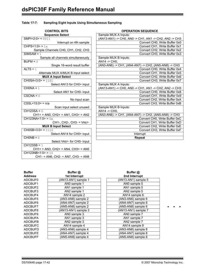
dsPIC30F Family Reference Manual
Table 17-7: Sampling Eight Inputs Using Simultaneous Sampling
CONTROL BITS OPERATION SEQUENCESequence Select Sample MUX A Inputs:
SMPI<2:0> = 0011 (AN13-AN1) -> CH0, AN0 -> CH1, AN1 -> CH2, AN2 -> CH3Interrupt on 4th sample Convert CH0, Write Buffer 0x0
CHPS<1:0> = 1x Convert CH1, Write Buffer 0x1Sample Channels CH0, CH1, CH2, CH3 Convert CH2, Write Buffer 0x2
SIMSAM = 1 Convert CH3, Write Buffer 0x3Sample all channels simultaneously Sample MUX B Inputs:
BUFM = 0 AN14 -> CH0, Single 16-word result buffer (AN3-AN6) -> CH1, (AN4-AN7) -> CH2, (AN5-AN8) -> CH3
ALTS = 1 Convert CH0, Write Buffer 0x4Alternate MUX A/MUX B input select Convert CH1, Write Buffer 0x5
MUX A Input Select Convert CH2, Write Buffer 0x6CH0SA<3:0> = 1101 Convert CH3, Write Buffer 0x7
Select AN13 for CH0+ input Sample MUX A Inputs: CH0NA = 1 (AN13-AN1) -> CH0, AN0 -> CH1, AN1 -> CH2, AN2 -> CH3
Select AN1 for CH0- input Convert CH0, Write Buffer 0x8CSCNA = 0 Convert CH1, Write Buffer 0x9
No input scan Convert CH2, Write Buffer 0xACSSL<15:0> = n/a Convert CH3, Write Buffer 0xB
Scan input select unused Sample MUX B Inputs: CH123SA = 0 AN14 -> CH0,
CH1+ = AN0, CH2+ = AN1, CH3+ = AN2 (AN3-AN6) -> CH1, (AN4-AN7) -> CH2, (AN5-AN8) -> CH3CH123NA<1:0> = 0x Convert CH0, Write Buffer 0xC
CH1-, CH2-, CH3- = VREF- Convert CH1, Write Buffer 0xDMUX B Input Select Convert CH2, Write Buffer 0xE
CH0SB<3:0> = 1110 Convert CH3, Write Buffer 0xFSelect AN14 for CH0+ input Interrupt
CH0NB = 0 RepeatSelect VREF- for CH0- input
CH123SB = 1CH1+ = AN3, CH2+ = AN4, CH3+ = AN5
CH123NB<1:0> = 10CH1- = AN6, CH2- = AN7, CH3- = AN8
BufferAddress
Buffer @1st Interrupt
Buffer @2nd Interrupt
ADCBUF0 (AN13-AN1) sample 1 (AN13-AN1) sample 5ADCBUF1 AN0 sample 1 AN0 sample 5ADCBUF2 AN1 sample 1 AN1 sample 5ADCBUF3 AN2 sample 1 AN2 sample 5ADCBUF4 AN14 sample 2 AN14 sample 6ADCBUF5 (AN3-AN6) sample 2 (AN3-AN6) sample 6ADCBUF6 (AN4-AN7) sample 2 (AN4-AN7) sample 6ADCBUF7 (AN5-AN8) sample 2 (AN5-AN8) sample 6 • • •ADCBUF8 (AN13-AN1) sample 3 (AN13-AN1) sample 7ADCBUF9 AN0 sample 3 AN0 sample 7ADCBUFA AN1 sample 3 AN1 sample 7ADCBUFB AN2 sample 3 AN2 sample 7ADCBUFC AN14 sample 4 AN14 sample 8ADCBUFD (AN3-AN6) sample 4 (AN3-AN6) sample 8ADCBUFE (AN4-AN7) sample 4 (AN4-AN7) sample 8ADCBUFF (AN5-AN8) sample 4 (AN5-AN8) sample 8
DS70064E-page 17-42 © 2007 Microchip Technology Inc.

Section 17. 10-bit A/D Converter10-bit A
/DC
onverter
17
17.16.7 Example: Sampling Eight Inputs Using Sequential Sampling
Figure 17-20 and Table 17-8 demonstrate sequential sampling. When converting more than onechannel and selecting sequential sampling, the module will start sampling a channel at theearliest opportunity, then perform the required conversions in sequence. In this example, withASAM set, sampling of a channel will begin after the conversion of that channel completes.
When ASAM is clear, sampling will not resume after conversion completion but will occur whensetting the SAMP bit.
When utilizing more than one channel, sequential sampling provides more sampling time sincea channel may be sampled while conversion occurs on another.
Figure 17-20: Sampling Eight Inputs Using Sequential Sampling
ADCLK
SAMP
DONE
Input to CH0 AN13-AN1
TSAMP
ADIF
AN0
AN1
AN2
Input to CH1
Input to CH2
Input to CH3
ADCBUFD
ADCBUFE
ADCBUFF
AN14
TSAMP
AN4-AN7
AN5-AN8
AN14
TSAMP
AN3-AN6
AN4-AN7
AN5-AN8
ASAM
AN1
AN2
ADCBUF0
ADCBUF1
ADCBUF2
ADCBUF3
ADCBUFC
AN13-AN1
AN0
AN2
ConversionTrigger
TCONVTCONVTCONVTCONV TCONVTCONVTCONVTCONV TCONVTCONVTCONVTCONV
AN3-AN6
AN1
AN13-AN1
AN0
© 2007 Microchip Technology Inc. DS70064E-page 17-43
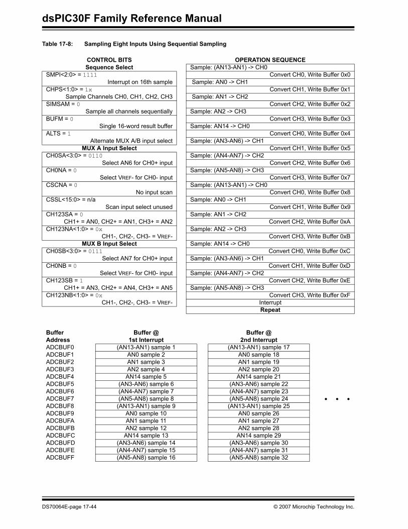
dsPIC30F Family Reference Manual
Table 17-8: Sampling Eight Inputs Using Sequential Sampling
CONTROL BITS OPERATION SEQUENCESequence Select Sample: (AN13-AN1) -> CH0
SMPI<2:0> = 1111 Convert CH0, Write Buffer 0x0Interrupt on 16th sample Sample: AN0 -> CH1
CHPS<1:0> = 1x Convert CH1, Write Buffer 0x1Sample Channels CH0, CH1, CH2, CH3 Sample: AN1 -> CH2
SIMSAM = 0 Convert CH2, Write Buffer 0x2Sample all channels sequentially Sample: AN2 -> CH3
BUFM = 0 Convert CH3, Write Buffer 0x3Single 16-word result buffer Sample: AN14 -> CH0
ALTS = 1 Convert CH0, Write Buffer 0x4Alternate MUX A/B input select Sample: (AN3-AN6) -> CH1
MUX A Input Select Convert CH1, Write Buffer 0x5CH0SA<3:0> = 0110 Sample: (AN4-AN7) -> CH2
Select AN6 for CH0+ input Convert CH2, Write Buffer 0x6CH0NA = 0 Sample: (AN5-AN8) -> CH3
Select VREF- for CH0- input Convert CH3, Write Buffer 0x7CSCNA = 0 Sample: (AN13-AN1) -> CH0
No input scan Convert CH0, Write Buffer 0x8CSSL<15:0> = n/a Sample: AN0 -> CH1
Scan input select unused Convert CH1, Write Buffer 0x9CH123SA = 0 Sample: AN1 -> CH2
CH1+ = AN0, CH2+ = AN1, CH3+ = AN2 Convert CH2, Write Buffer 0xACH123NA<1:0> = 0x Sample: AN2 -> CH3
CH1-, CH2-, CH3- = VREF- Convert CH3, Write Buffer 0xBMUX B Input Select Sample: AN14 -> CH0
CH0SB<3:0> = 0111 Convert CH0, Write Buffer 0xCSelect AN7 for CH0+ input Sample: (AN3-AN6) -> CH1
CH0NB = 0 Convert CH1, Write Buffer 0xDSelect VREF- for CH0- input Sample: (AN4-AN7) -> CH2
CH123SB = 1 Convert CH2, Write Buffer 0xECH1+ = AN3, CH2+ = AN4, CH3+ = AN5 Sample: (AN5-AN8) -> CH3
CH123NB<1:0> = 0x Convert CH3, Write Buffer 0xFCH1-, CH2-, CH3- = VREF- Interrupt
Repeat
BufferAddress
Buffer @1st Interrupt
Buffer @2nd Interrupt
ADCBUF0 (AN13-AN1) sample 1 (AN13-AN1) sample 17ADCBUF1 AN0 sample 2 AN0 sample 18ADCBUF2 AN1 sample 3 AN1 sample 19ADCBUF3 AN2 sample 4 AN2 sample 20ADCBUF4 AN14 sample 5 AN14 sample 21ADCBUF5 (AN3-AN6) sample 6 (AN3-AN6) sample 22ADCBUF6 (AN4-AN7) sample 7 (AN4-AN7) sample 23ADCBUF7 (AN5-AN8) sample 8 (AN5-AN8) sample 24 • • •ADCBUF8 (AN13-AN1) sample 9 (AN13-AN1) sample 25ADCBUF9 AN0 sample 10 AN0 sample 26ADCBUFA AN1 sample 11 AN1 sample 27ADCBUFB AN2 sample 12 AN2 sample 28ADCBUFC AN14 sample 13 AN14 sample 29ADCBUFD (AN3-AN6) sample 14 (AN3-AN6) sample 30ADCBUFE (AN4-AN7) sample 15 (AN4-AN7) sample 31ADCBUFF (AN5-AN8) sample 16 (AN5-AN8) sample 32
DS70064E-page 17-44 © 2007 Microchip Technology Inc.
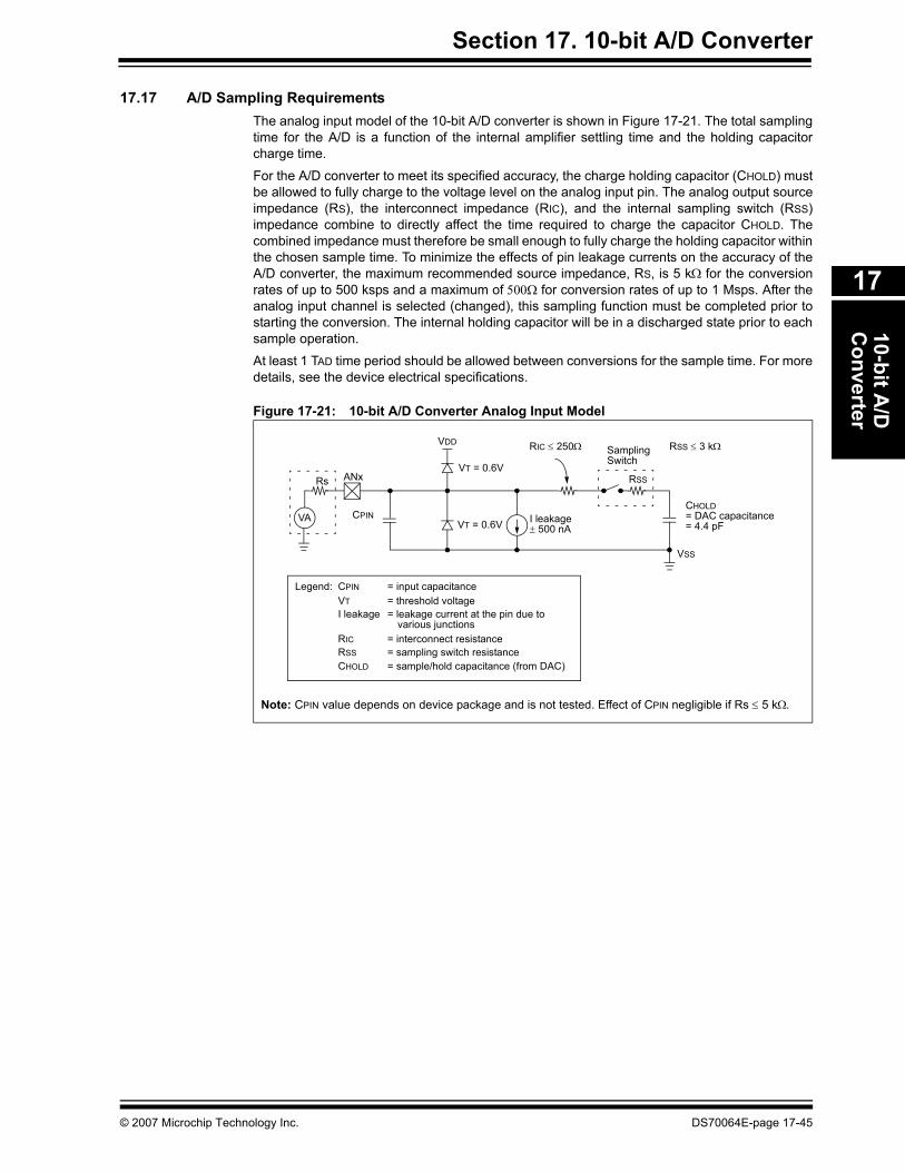
Section 17. 10-bit A/D Converter10-bit A
/DC
onverter
17
17.17 A/D Sampling Requirements The analog input model of the 10-bit A/D converter is shown in Figure 17-21. The total samplingtime for the A/D is a function of the internal amplifier settling time and the holding capacitorcharge time.
For the A/D converter to meet its specified accuracy, the charge holding capacitor (CHOLD) mustbe allowed to fully charge to the voltage level on the analog input pin. The analog output sourceimpedance (RS), the interconnect impedance (RIC), and the internal sampling switch (RSS)impedance combine to directly affect the time required to charge the capacitor CHOLD. Thecombined impedance must therefore be small enough to fully charge the holding capacitor withinthe chosen sample time. To minimize the effects of pin leakage currents on the accuracy of theA/D converter, the maximum recommended source impedance, RS, is 5 kΩ for the conversionrates of up to 500 ksps and a maximum of 500Ω for conversion rates of up to 1 Msps. After theanalog input channel is selected (changed), this sampling function must be completed prior tostarting the conversion. The internal holding capacitor will be in a discharged state prior to eachsample operation.
At least 1 TAD time period should be allowed between conversions for the sample time. For moredetails, see the device electrical specifications.
Figure 17-21: 10-bit A/D Converter Analog Input Model
CPINVA
Rs ANxVT = 0.6V
VT = 0.6V I leakage
RIC ≤ 250Ω SamplingSwitch
RSS
CHOLD= DAC capacitance
VSS
VDD
= 4.4 pF± 500 nA
Legend: CPIN
VTI leakage
RICRSS
CHOLD
= input capacitance= threshold voltage= leakage current at the pin due to
= interconnect resistance= sampling switch resistance= sample/hold capacitance (from DAC)
various junctions
Note: CPIN value depends on device package and is not tested. Effect of CPIN negligible if Rs ≤ 5 kΩ.
RSS ≤ 3 kΩ
© 2007 Microchip Technology Inc. DS70064E-page 17-45
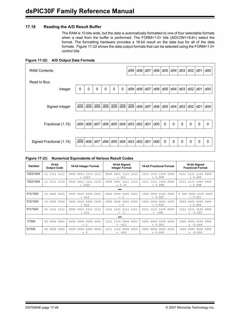
dsPIC30F Family Reference Manual
17.18 Reading the A/D Result BufferThe RAM is 10 bits wide, but the data is automatically formatted to one of four selectable formatswhen a read from the buffer is performed. The FORM<1:0> bits (ADCON1<9:8>) select theformat. The formatting hardware provides a 16-bit result on the data bus for all of the dataformats. Figure 17-22 shows the data output formats that can be selected using the FORM<1:0>control bits.
Figure 17-22: A/D Output Data Formats
Figure 17-23: Numerical Equivalents of Various Result Codes
RAM Contents: d09 d08 d07 d06 d05 d04 d03 d02 d01 d00
Read to Bus:
Integer 0 0 0 0 0 0 d09 d08 d07 d06 d05 d04 d03 d02 d01 d00
Signed Integer d09 d09 d09 d09 d09 d09 d09 d08 d07 d06 d05 d04 d03 d02 d01 d00
Fractional (1.15) d09 d08 d07 d06 d05 d04 d03 d02 d01 d00 0 0 0 0 0 0
Signed Fractional (1.15) d09 d08 d07 d06 d05 d04 d03 d02 d01 d00 0 0 0 0 0 0
VIN/VREF10-bit
Output Code 16-bit Integer Format 16-bit SignedInteger Format 16-bit Fractional Format 16-bit Signed
Fractional Format
1023/1024 11 1111 1111 0000 0011 1111 1111= 1023
0000 0001 1111 1111= 511
1111 1111 1100 0000= 0.999
0111 1111 1100 0000= 0.499
1022/1024 11 1111 1110 0000 0011 1111 1110= 1022
0000 0001 1111 1110= 5 10
1111 1111 1000 0000= 0.998
0111 1111 1000 0000= 0.498
•••
513/1024 10 0000 0001 0000 0010 0000 0001= 513
0000 0000 0000 0001= 1
1000 0000 0100 0000= 0.501
0 000 0000 0100 0000= 0.001
512/1024 10 0000 0000 0000 0010 0000 0000= 512
0000 0000 0000 0000= 0
1000 0000 0000 0000= 0.500
0000 0000 0000 0000= 0.000
511/1024 01 1111 1111 0000 0001 1111 1111= 511
1111 1111 1111 1111= -1
0111 1111 1100 0000= .499
1111 1111 1100 0000= -0.001
•••
1/1024 00 0000 0001 0000 0000 0000 0001= 1
1111 1110 0000 0001= -511
0000 0000 0100 0000= 0.001
1000 0000 0100 0000= -0.499
0/1024 00 0000 0000 0000 0000 0000 0000= 0
1111 1110 0000 0000= -512
0000 0000 0000 0000= 0.000
1000 0000 0000 0000= -0.500
DS70064E-page 17-46 © 2007 Microchip Technology Inc.

Section 17. 10-bit A/D Converter10-bit A
/DC
onverter
17
17.19 Transfer FunctionThe ideal transfer function of the A/D converter is shown in Figure 17-24. The difference of theinput voltages, (VINH – VINL), is compared to the reference, (VREFH – VREFL).
• The first code transition occurs when the input voltage is (VREFH – VREFL/2048) or 0.5 LSb. • The 00 0000 0001 code is centered at (VREFH – VREFL/1024) or 1.0 LSb. • The 10 0000 0000 code is centered at (512*(VREFH – VREFL)/1024).• An input voltage less than (1*(VREFH – VREFL)/2048) converts as 00 0000 0000.• An input greater than (2045*(VREFH – VREFL)/2048) converts as 11 1111 1111.
Figure 17-24: A/D Transfer Function
17.20 A/D Accuracy/ErrorRefer to Section 17.28 “Related Application Notes”for a list of documents that discuss A/Daccuracy.
17.21 Connection Considerations Since the analog inputs employ ESD protection, they have diodes to VDD and VSS. This requiresthat the analog input must be between VDD and VSS. If the input voltage exceeds this range bygreater than 0.3V (either direction), one of the diodes becomes forward biased and it maydamage the device if the input current specification is exceeded.
An external RC filter is sometimes added for anti-aliasing of the input signal. The R componentshould be selected to ensure that the sampling time requirements are satisfied. Any externalcomponents connected (via high-impedance) to an analog input pin (capacitor, zener diode, etc.)should have very little leakage current at the pin.
10 0000 0010 (= 514)
10 0000 0011 (= 515)
01 1111 1101 (= 509)
01 1111 1110 (= 510)
01 1111 1111 (= 511)
11 1111 1110 (= 1022)
11 1111 1111 (= 1023)
00 0000 0000 (= 0)
00 0000 0001 (= 1)
Output Code
10 0000 0000 (= 512)
(VINH – VINL)
VREFL VREFH – VREFL
1024
VREFHVREFL +
10 0000 0001 (= 513)
512*(VREFH – VREFL)1024
VREFL + 1023*(VREFH – VREFL)1024
VREFL +
© 2007 Microchip Technology Inc. DS70064E-page 17-47
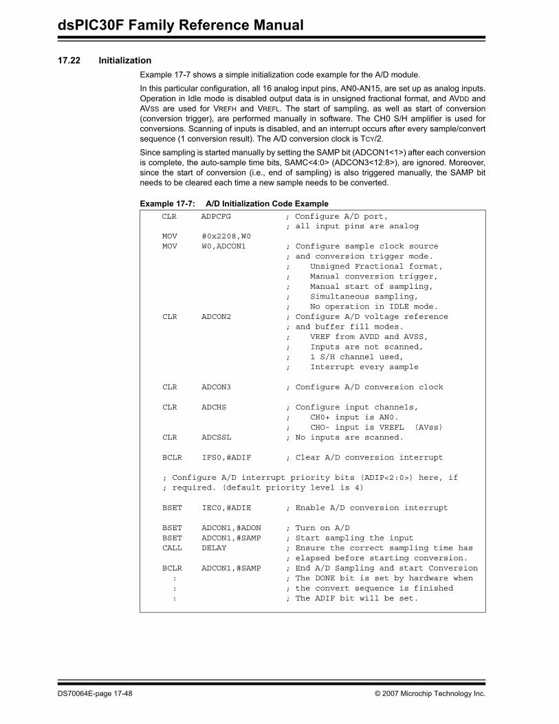
dsPIC30F Family Reference Manual
17.22 InitializationExample 17-7 shows a simple initialization code example for the A/D module.
In this particular configuration, all 16 analog input pins, AN0-AN15, are set up as analog inputs.Operation in Idle mode is disabled output data is in unsigned fractional format, and AVDD andAVSS are used for VREFH and VREFL. The start of sampling, as well as start of conversion(conversion trigger), are performed manually in software. The CH0 S/H amplifier is used forconversions. Scanning of inputs is disabled, and an interrupt occurs after every sample/convertsequence (1 conversion result). The A/D conversion clock is TCY/2.
Since sampling is started manually by setting the SAMP bit (ADCON1<1>) after each conversionis complete, the auto-sample time bits, SAMC<4:0> (ADCON3<12:8>), are ignored. Moreover,since the start of conversion (i.e., end of sampling) is also triggered manually, the SAMP bitneeds to be cleared each time a new sample needs to be converted.
Example 17-7: A/D Initialization Code Example CLR ADPCFG ; Configure A/D port, ; all input pins are analog MOV #0x2208,W0 MOV W0,ADCON1 ; Configure sample clock source ; and conversion trigger mode. ; Unsigned Fractional format, ; Manual conversion trigger, ; Manual start of sampling, ; Simultaneous sampling, ; No operation in IDLE mode. CLR ADCON2 ; Configure A/D voltage reference ; and buffer fill modes. ; VREF from AVDD and AVSS, ; Inputs are not scanned, ; 1 S/H channel used, ; Interrupt every sample CLR ADCON3 ; Configure A/D conversion clock CLR ADCHS ; Configure input channels, ; CH0+ input is AN0. ; CHO- input is VREFL (AVss) CLR ADCSSL ; No inputs are scanned.
BCLR IFS0,#ADIF ; Clear A/D conversion interrupt
; Configure A/D interrupt priority bits (ADIP<2:0>) here, if ; required. (default priority level is 4)
BSET IEC0,#ADIE ; Enable A/D conversion interrupt BSET ADCON1,#ADON ; Turn on A/D BSET ADCON1,#SAMP ; Start sampling the input CALL DELAY ; Ensure the correct sampling time has ; elapsed before starting conversion. BCLR ADCON1,#SAMP ; End A/D Sampling and start Conversion : ; The DONE bit is set by hardware when : ; the convert sequence is finished : ; The ADIF bit will be set.
DS70064E-page 17-48 © 2007 Microchip Technology Inc.

Section 17. 10-bit A/D Converter10-bit A
/DC
onverter
17
17.23 A/D Conversion SpeedsThe dsPIC30F 10-bit A/D converter specifications permit a maximum 1 Msps sampling rate. Thetable below summarizes the conversion speeds for the dsPIC30F 10-bit A/D converter and therequired operating conditions.
Table 17-9: 10-bit Conversion Rate Parameters
dsPIC30F 10-bit A/D Converter Conversion Rates
A/D Speed TAD Minimum
Sampling Time Min Rs Max VDD Temperature A/D Channels Configuration
Up to 1 Msps(1)
83.33 ns 12 TAD 500 Ω 4.5V to 5.5V -40°C to +85°C
Up to 750 ksps(1)
95.24 ns 2 TAD 500 Ω 4.5V to 5.5V -40°C to +85°C
Up to 600 ksps(1)
138.89 ns 12 TAD 500 Ω 3.0V to 5.5V -40°C to +125°C
Up to 500 ksps
153.85 ns 1 TAD 5.0 kΩ 4.5V to 5.5V -40°C to +125°C
Up to 300 ksps
256.41 ns 1 TAD 5.0 kΩ 3.0V to 5.5V -40°C to +125°C
Note 1: External VREF- and VREF+ pins must be used for correct operation. See Figure 17-25 for recommendedcircuit.
VREF- VREF+
ADC
ANxS/H
S/H
CH1, CH2 or CH3
CH0
VREF- VREF+
ADCANx
S/HCHX
VREF- VREF+
ADC
ANxS/H
S/H
CH1, CH2 or CH3
CH0
VREF- VREF+
ADCANx
S/HCHX
ANx or VREF-
orAVSS
orAVDD
VREF- VREF+
ADCANx
S/HCHX
ANx or VREF-
orAVSS
orAVDD
© 2007 Microchip Technology Inc. DS70064E-page 17-49
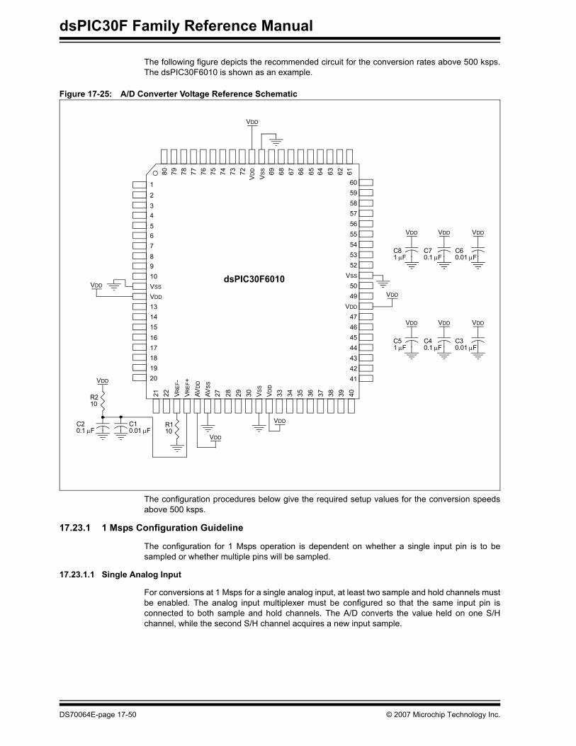
dsPIC30F Family Reference Manual
The following figure depicts the recommended circuit for the conversion rates above 500 ksps.The dsPIC30F6010 is shown as an example.
Figure 17-25: A/D Converter Voltage Reference Schematic
The configuration procedures below give the required setup values for the conversion speedsabove 500 ksps.
17.23.1 1 Msps Configuration Guideline
The configuration for 1 Msps operation is dependent on whether a single input pin is to besampled or whether multiple pins will be sampled.
17.23.1.1 Single Analog Input
For conversions at 1 Msps for a single analog input, at least two sample and hold channels mustbe enabled. The analog input multiplexer must be configured so that the same input pin isconnected to both sample and hold channels. The A/D converts the value held on one S/Hchannel, while the second S/H channel acquires a new input sample.
7274 73
VDD
VS
S 69 68 67 66 65 64 63 62 61
20
2345678910VSS
VDD
13141516
5049
VDD
47464544
21
41
40393837363534VRE
F-V R
EF+
AVD
D
AVS
S
27 28 29 30 V SS
VDD
33
171819
75
1
575655545352
VSS
605958
4342
7678 777922
80
dsPIC30F6010
VDD
VDD
VDD
VDD
VDD
VDD
VDD
R210
C20.1 μF
C10.01 μF
R110
C81 μF
VDD
C70.1 μF
VDD
C60.01 μF
VDD
C51 μF
VDD
C40.1 μF
VDD
C30.01 μF
DS70064E-page 17-50 © 2007 Microchip Technology Inc.
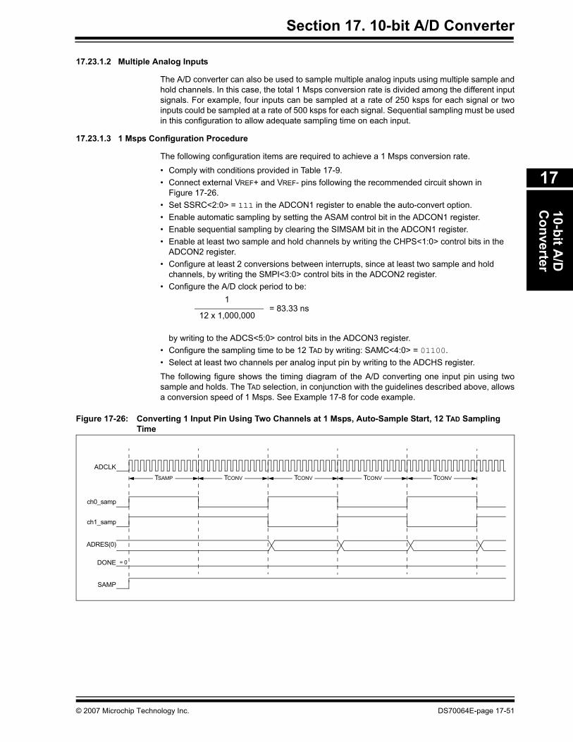
Section 17. 10-bit A/D Converter10-bit A
/DC
onverter
17
17.23.1.2 Multiple Analog Inputs
The A/D converter can also be used to sample multiple analog inputs using multiple sample andhold channels. In this case, the total 1 Msps conversion rate is divided among the different inputsignals. For example, four inputs can be sampled at a rate of 250 ksps for each signal or twoinputs could be sampled at a rate of 500 ksps for each signal. Sequential sampling must be usedin this configuration to allow adequate sampling time on each input.
17.23.1.3 1 Msps Configuration Procedure
The following configuration items are required to achieve a 1 Msps conversion rate.
• Comply with conditions provided in Table 17-9.• Connect external VREF+ and VREF- pins following the recommended circuit shown in
Figure 17-26.• Set SSRC<2:0> = 111 in the ADCON1 register to enable the auto-convert option.• Enable automatic sampling by setting the ASAM control bit in the ADCON1 register.• Enable sequential sampling by clearing the SIMSAM bit in the ADCON1 register.• Enable at least two sample and hold channels by writing the CHPS<1:0> control bits in the
ADCON2 register.• Configure at least 2 conversions between interrupts, since at least two sample and hold
channels, by writing the SMPI<3:0> control bits in the ADCON2 register.• Configure the A/D clock period to be:
by writing to the ADCS<5:0> control bits in the ADCON3 register.• Configure the sampling time to be 12 TAD by writing: SAMC<4:0> = 01100.• Select at least two channels per analog input pin by writing to the ADCHS register.
The following figure shows the timing diagram of the A/D converting one input pin using twosample and holds. The TAD selection, in conjunction with the guidelines described above, allowsa conversion speed of 1 Msps. See Example 17-8 for code example.
Figure 17-26: Converting 1 Input Pin Using Two Channels at 1 Msps, Auto-Sample Start, 12 TAD Sampling Time
1
12 x 1,000,000= 83.33 ns
TCONV
ADCLK
ch0_samp
ch1_samp
ADRES(0)
DONE
TSAMP TCONV TCONV TCONV
SAMP
= 0
© 2007 Microchip Technology Inc. DS70064E-page 17-51
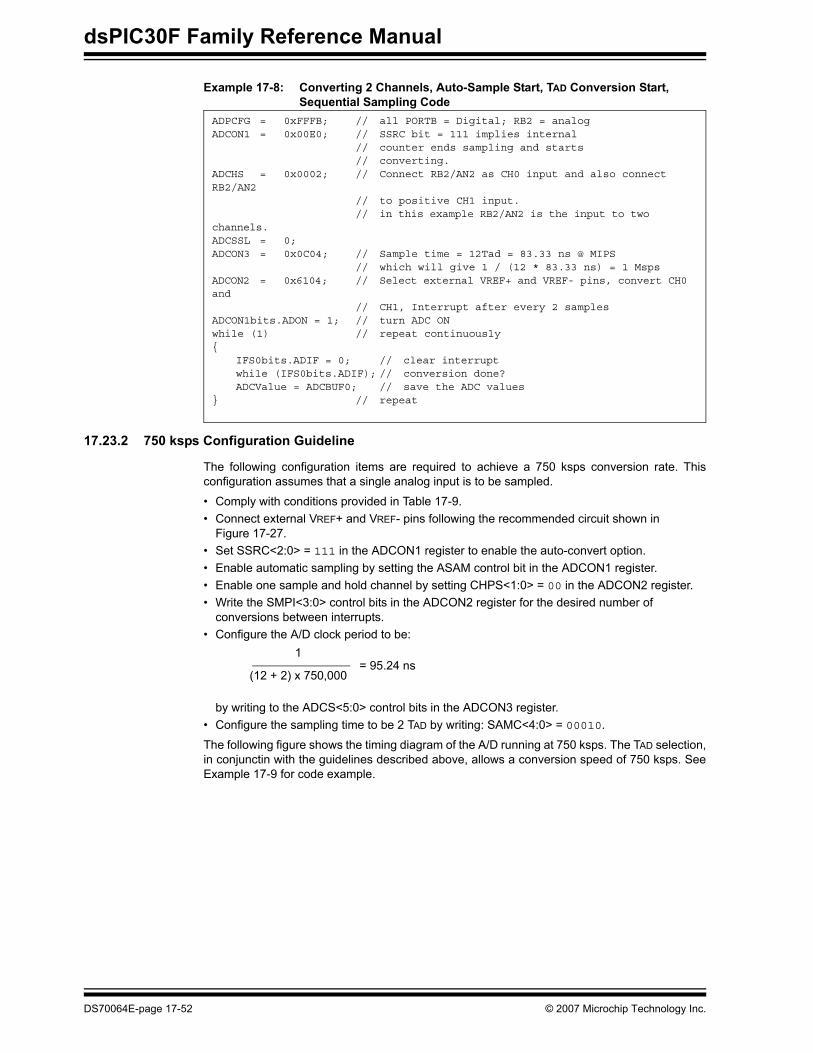
dsPIC30F Family Reference Manual
Example 17-8: Converting 2 Channels, Auto-Sample Start, TAD Conversion Start, Sequential Sampling Code
17.23.2 750 ksps Configuration Guideline
The following configuration items are required to achieve a 750 ksps conversion rate. Thisconfiguration assumes that a single analog input is to be sampled.
• Comply with conditions provided in Table 17-9.• Connect external VREF+ and VREF- pins following the recommended circuit shown in
Figure 17-27.• Set SSRC<2:0> = 111 in the ADCON1 register to enable the auto-convert option.• Enable automatic sampling by setting the ASAM control bit in the ADCON1 register.• Enable one sample and hold channel by setting CHPS<1:0> = 00 in the ADCON2 register.• Write the SMPI<3:0> control bits in the ADCON2 register for the desired number of
conversions between interrupts.• Configure the A/D clock period to be:
by writing to the ADCS<5:0> control bits in the ADCON3 register.• Configure the sampling time to be 2 TAD by writing: SAMC<4:0> = 00010.
The following figure shows the timing diagram of the A/D running at 750 ksps. The TAD selection,in conjunctin with the guidelines described above, allows a conversion speed of 750 ksps. SeeExample 17-9 for code example.
ADPCFG = 0xFFFB; // all PORTB = Digital; RB2 = analogADCON1 = 0x00E0; // SSRC bit = 111 implies internal
// counter ends sampling and starts// converting.
ADCHS = 0x0002; // Connect RB2/AN2 as CH0 input and also connect RB2/AN2
// to positive CH1 input.// in this example RB2/AN2 is the input to two
channels.ADCSSL = 0;ADCON3 = 0x0C04; // Sample time = 12Tad = 83.33 ns @ MIPS
// which will give 1 / (12 * 83.33 ns) = 1 MspsADCON2 = 0x6104; // Select external VREF+ and VREF- pins, convert CH0 and
// CH1, Interrupt after every 2 samplesADCON1bits.ADON = 1; // turn ADC ONwhile (1) // repeat continuously{
IFS0bits.ADIF = 0; // clear interruptwhile (IFS0bits.ADIF); // conversion done?ADCValue = ADCBUF0; // save the ADC values
} // repeat
1
(12 + 2) x 750,000= 95.24 ns
DS70064E-page 17-52 © 2007 Microchip Technology Inc.
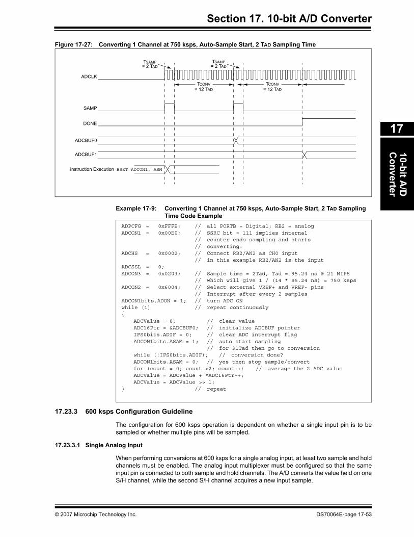
Section 17. 10-bit A/D Converter10-bit A
/DC
onverter
17
Figure 17-27: Converting 1 Channel at 750 ksps, Auto-Sample Start, 2 TAD Sampling Time
Example 17-9: Converting 1 Channel at 750 ksps, Auto-Sample Start, 2 TAD Sampling Time Code Example
17.23.3 600 ksps Configuration Guideline
The configuration for 600 ksps operation is dependent on whether a single input pin is to besampled or whether multiple pins will be sampled.
17.23.3.1 Single Analog Input
When performing conversions at 600 ksps for a single analog input, at least two sample and holdchannels must be enabled. The analog input multiplexer must be configured so that the sameinput pin is connected to both sample and hold channels. The A/D converts the value held on oneS/H channel, while the second S/H channel acquires a new input sample.
TCONV= 12 TAD
TCONV= 12 TAD
TSAMP= 2 TAD
TSAMP= 2 TAD
ADCLK
SAMP
DONE
ADCBUF0
ADCBUF1
Instruction Execution BSET ADCON1, ASM
ADPCFG = 0xFFFB; // all PORTB = Digital; RB2 = analogADCON1 = 0x00E0; // SSRC bit = 111 implies internal
// counter ends sampling and starts// converting.
ADCHS = 0x0002; // Connect RB2/AN2 as CH0 input// in this example RB2/AN2 is the input
ADCSSL = 0;ADCON3 = 0x0203; // Sample time = 2Tad, Tad = 95.24 ns @ 21 MIPS
// which will give 1 / (14 * 95.24 ns) = 750 kspsADCON2 = 0x6004; // Select external VREF+ and VREF- pins
// Interrupt after every 2 samplesADCON1bits.ADON = 1; // turn ADC ONwhile (1) // repeat continuously{
ADCValue = 0; // clear valueADC16Ptr = &ADCBUF0; // initialize ADCBUF pointerIFS0bits.ADIF = 0; // clear ADC interrupt flagADCON1bits.ASAM = 1; // auto start sampling
// for 31Tad then go to conversionwhile (!IFS0bits.ADIF); // conversion done?ADCON1bits.ASAM = 0; // yes then stop sample/convertfor (count = 0; count <2; count++) // average the 2 ADC valueADCValue = ADCValue + *ADC16Ptr++;ADCValue = ADCValue >> 1;
} // repeat
© 2007 Microchip Technology Inc. DS70064E-page 17-53
dsPIC30F Family Reference Manual
17.23.3.2 Multiple Analog Inputs
The A/D converter can also be used to sample multiple analog inputs using multiple sample andhold channels. In this case, the total 600 ksps conversion rate is divided among the different inputsignals. For example, four inputs can be sampled at a rate of 150 ksps for each signal or twoinputs could be sampled at a rate of 300 ksps for each signal. Sequential sampling must be usedin this configuration to allow adequate sampling time on each input.
17.23.3.3 600 ksps Configuration Items
The following configuration items are required to achieve a 600 ksps conversion rate.
• Comply with conditions provided in Table 17-9.• Connect external VREF+ and VREF- pins following the recommended circuit shown in
Figure 17-10.• Set SSRC<2:0> = 111 in the ADCON1 register to enable the auto-convert option.• Enable automatic sampling by setting the ASAM control bit in the ADCON1 register.• Enable sequential sampling by clearing the SIMSAM bit in the ADCON1 register.• Enable at least two sample and hold channels by writing the CHPS<1:0> control bits in the
ADCON2 register.• Configure at least 2 conversions between interrupts, since at least two sample and hold
channels, by writing the SMPI<3:0> control bits in the ADCON2 register.• Configure the A/D clock period to be:
by writing to the ADCS<5:0> control bits in the ADCON3 register.• Configure the sampling time to be 2 TAD by writing: SAMC<4:0> = 00010.• Select at least two channels per analog input pin by writing to the ADCHS register.
The timing diagram for the 600 ksps extended rate is the same as for the 1 Msps shown inFigure 17-10. See Example 17-10 for code example for 600 ksps A/D operation.
Example 17-10: Converting 2 Channels, Auto-Sample Start, TAD Conversion Start, Sequential Sampling Code
1
12 x 600,000= 138.89 ns
ADPCFG = 0xFFFB; // all PORTB = Digital; RB2 = analogADCON1 = 0x00E0; // SSRC bit = 111 implies internal
// counter ends sampling and starts// converting.
ADCHS = 0x0002; // Connect RB2/AN2 as CH0 input and also connect RB2/AN2
// to positive CH1 input.// in this example RB2/AN2 is the input to two
channels.ADCSSL = 0;ADCON3 = 0x0C04; // Sample time = 12Tad = 138.89 ns @ 18 MIPS
// which will give 1 / (12 * 138.89 ns) = 600 kspsADCON2 = 0x6104; // Select external VREF+ and VREF- pins, convert CH0 and
// CH1, Interrupt after every 2 samplesADCON1bits.ADON = 1; // turn ADC ONwhile (1) // repeat continuously{
IFS0bits.ADIF = 0; // clear interruptwhile (IFS0bits.ADIF); // conversion done?ADCValue = ADCBUF0; // save the ADC values
} // repeat
DS70064E-page 17-54 © 2007 Microchip Technology Inc.
Section 17. 10-bit A/D Converter10-bit A
/DC
onverter
17
17.24 Operation During Sleep and Idle Modes Sleep and Idle modes are useful for minimizing conversion noise because the digital activity ofthe CPU, buses and other peripherals is minimized.
17.24.1 CPU Sleep Mode without RC A/D Clock
When the device enters Sleep mode, all clock sources to the module are shutdown and stay atlogic ‘0’.
If Sleep occurs in the middle of a conversion, the conversion is aborted unless the A/D is clockedfrom its internal RC clock generator. The converter will not resume a partially completedconversion on exiting from Sleep mode.
Register contents are not affected by the device entering or leaving Sleep mode.
17.24.2 CPU Sleep Mode with RC A/D Clock
The A/D module can operate during Sleep mode if the A/D clock source is set to the internal A/DRC oscillator (ADRC = 1). This eliminates digital switching noise from the conversion. When theconversion is completed, the DONE bit will be set and the result loaded into the A/D result buffer,ADCBUF.
If the A/D interrupt is enabled (ADIE = 1), the device will wake-up from Sleep when the A/Dinterrupt occurs. Program execution will resume at the A/D Interrupt Service Routine (ISR) if theA/D interrupt is greater than the current CPU priority. Otherwise, execution will continue from theinstruction after the PWRSAV instruction that placed the device in Sleep mode.
If the A/D interrupt is not enabled, the A/D module will then be turned off, although the ADON bitwill remain set.
To minimize the effects of digital noise on the A/D module operation, the user should select aconversion trigger source that ensures the A/D conversion will take place in Sleep mode. Theautomatic conversion trigger option can be used for sampling and conversion in Sleep(SSRC<2:0> = 111). To use the automatic conversion option, the ADON bit should be set in theinstruction prior to the PWRSAV instruction.
17.24.3 A/D Operation During CPU Idle Mode
For the A/D, the ADSIDL bit (ADCON1<13>) selects if the module will stop on Idle or continueon Idle. If ADSIDL = 0, the module will continue normal operation when the device enters Idlemode. If the A/D interrupt is enabled (ADIE = 1), the device will wake up from Idle mode whenthe A/D interrupt occurs. Program execution will resume at the A/D Interrupt Service Routine ifthe A/D interrupt is greater than the current CPU priority. Otherwise, execution will continue fromthe instruction after the PWRSAV instruction that placed the device in Idle mode.
If ADSIDL = 1, the module will stop in Idle. If the device enters Idle mode in the middle of aconversion, the conversion is aborted. The converter will not resume a partially completedconversion on exiting from Idle mode.
17.25 Effects of a ResetA device Reset forces all registers to their Reset state. This forces the A/D module to be turnedoff, and any conversion in progress is aborted. All pins that are multiplexed with analog inputswill be configured as analog inputs. The corresponding TRIS bits will be set.
The values in the ADCBUF registers are not initialized during a Power-on Reset.ADCBUF0...ADCBUFF will contain unknown data.
Note: For the A/D module to operate in Sleep, the A/D clock source must be set to RC(ADRC = 1).
© 2007 Microchip Technology Inc. DS70064E-page 17-55
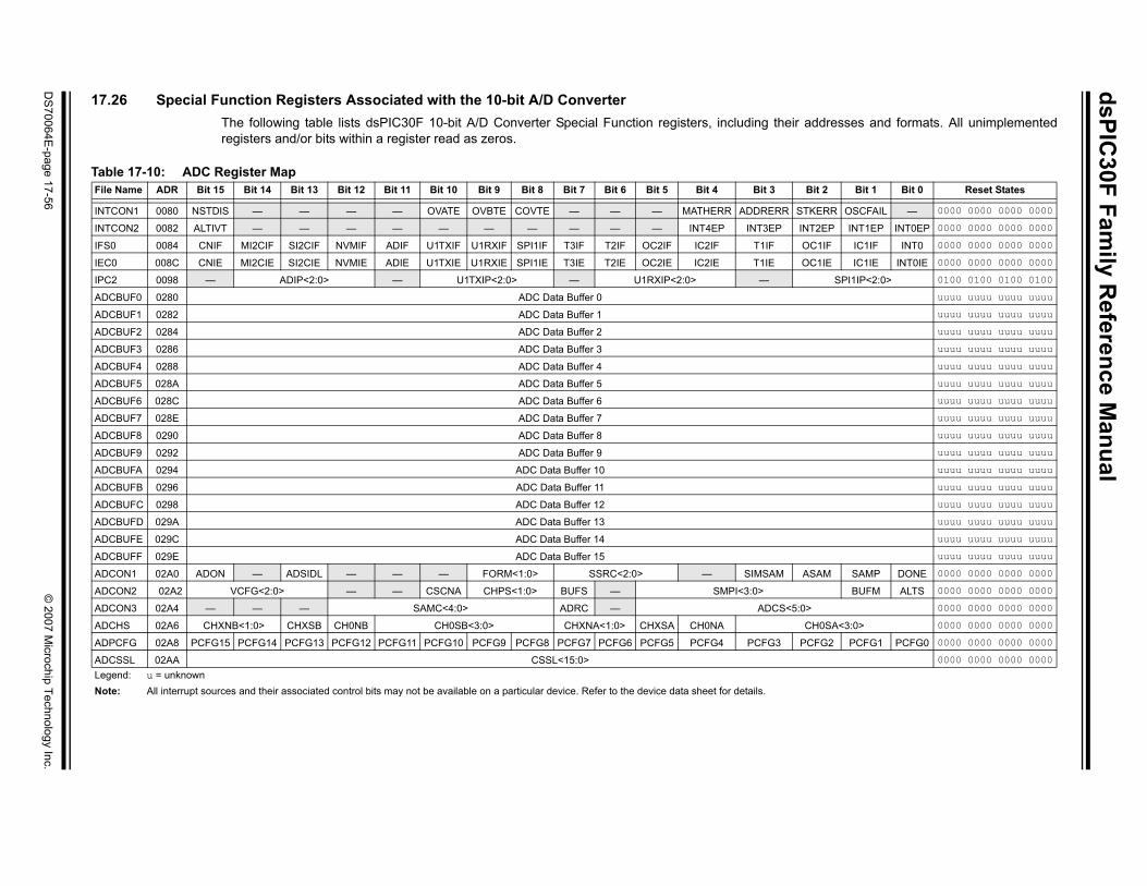
dsPIC30F Fam
ily Reference M
anual
DS
70064E-page 17-56
© 2007 M
icrochip Technology Inc.
ir addresses and formats. All unimplemented
Bit 2 Bit 1 Bit 0 Reset States
STKERR OSCFAIL — 0000 0000 0000 0000
INT2EP INT1EP INT0EP 0000 0000 0000 0000
OC1IF IC1IF INT0 0000 0000 0000 0000
OC1IE IC1IE INT0IE 0000 0000 0000 0000
SPI1IP<2:0> 0100 0100 0100 0100
uuuu uuuu uuuu uuuu
uuuu uuuu uuuu uuuu
uuuu uuuu uuuu uuuu
uuuu uuuu uuuu uuuu
uuuu uuuu uuuu uuuu
uuuu uuuu uuuu uuuu
uuuu uuuu uuuu uuuu
uuuu uuuu uuuu uuuu
uuuu uuuu uuuu uuuu
uuuu uuuu uuuu uuuu
uuuu uuuu uuuu uuuu
uuuu uuuu uuuu uuuu
uuuu uuuu uuuu uuuu
uuuu uuuu uuuu uuuu
uuuu uuuu uuuu uuuu
uuuu uuuu uuuu uuuu
ASAM SAMP DONE 0000 0000 0000 0000
BUFM ALTS 0000 0000 0000 0000
5:0> 0000 0000 0000 0000
CH0SA<3:0> 0000 0000 0000 0000
PCFG2 PCFG1 PCFG0 0000 0000 0000 0000
0000 0000 0000 0000
17.26 Special Function Registers Associated with the 10-bit A/D ConverterThe following table lists dsPIC30F 10-bit A/D Converter Special Function registers, including theregisters and/or bits within a register read as zeros.
Table 17-10: ADC Register MapFile Name ADR Bit 15 Bit 14 Bit 13 Bit 12 Bit 11 Bit 10 Bit 9 Bit 8 Bit 7 Bit 6 Bit 5 Bit 4 Bit 3
INTCON1 0080 NSTDIS — — — — OVATE OVBTE COVTE — — — MATHERR ADDRERR
INTCON2 0082 ALTIVT — — — — — — — — — — INT4EP INT3EP
IFS0 0084 CNIF MI2CIF SI2CIF NVMIF ADIF U1TXIF U1RXIF SPI1IF T3IF T2IF OC2IF IC2IF T1IF
IEC0 008C CNIE MI2CIE SI2CIE NVMIE ADIE U1TXIE U1RXIE SPI1IE T3IE T2IE OC2IE IC2IE T1IE
IPC2 0098 — ADIP<2:0> — U1TXIP<2:0> — U1RXIP<2:0> —
ADCBUF0 0280 ADC Data Buffer 0
ADCBUF1 0282 ADC Data Buffer 1
ADCBUF2 0284 ADC Data Buffer 2
ADCBUF3 0286 ADC Data Buffer 3
ADCBUF4 0288 ADC Data Buffer 4
ADCBUF5 028A ADC Data Buffer 5
ADCBUF6 028C ADC Data Buffer 6
ADCBUF7 028E ADC Data Buffer 7
ADCBUF8 0290 ADC Data Buffer 8
ADCBUF9 0292 ADC Data Buffer 9
ADCBUFA 0294 ADC Data Buffer 10
ADCBUFB 0296 ADC Data Buffer 11
ADCBUFC 0298 ADC Data Buffer 12
ADCBUFD 029A ADC Data Buffer 13
ADCBUFE 029C ADC Data Buffer 14
ADCBUFF 029E ADC Data Buffer 15
ADCON1 02A0 ADON — ADSIDL — — — FORM<1:0> SSRC<2:0> — SIMSAM
ADCON2 02A2 VCFG<2:0> — — CSCNA CHPS<1:0> BUFS — SMPI<3:0>
ADCON3 02A4 — — — SAMC<4:0> ADRC — ADCS<
ADCHS 02A6 CHXNB<1:0> CHXSB CH0NB CH0SB<3:0> CHXNA<1:0> CHXSA CH0NA
ADPCFG 02A8 PCFG15 PCFG14 PCFG13 PCFG12 PCFG11 PCFG10 PCFG9 PCFG8 PCFG7 PCFG6 PCFG5 PCFG4 PCFG3
ADCSSL 02AA CSSL<15:0>Legend: u = unknownNote: All interrupt sources and their associated control bits may not be available on a particular device. Refer to the device data sheet for details.

Section 17. 10-bit A/D Converter10-bit A
/DC
onverter
17
17.27 Design Tips
Question 1: How can I optimize the system performance of the A/D converter? Answer:1. Make sure you are meeting all of the timing specifications. If you are turning the module
off and on, there is a minimum delay you must wait before taking a sample. If you arechanging input channels, there is a minimum delay you must wait for this as well andfinally, there is TAD, which is the time selected for each bit conversion. This is selected inADCON3 and should be within a certain range as specified in the ElectricalCharacteristics. If TAD is too short, the result may not be fully converted before theconversion is terminated, and if TAD is made too long, the voltage on the samplingcapacitor can decay before the conversion is complete. These timing specifications areprovided in the “Electrical Specifications” section of the device data sheets.
2. Often the source impedance of the analog signal is high (greater than 10 kΩ), so thecurrent drawn from the source to charge the sample capacitor can affect accuracy. If theinput signal does not change too quickly, try putting a 0.1 μF capacitor on the analog input.This capacitor will charge to the analog voltage being sampled and supply theinstantaneous current needed to charge the 4.4 pF internal holding capacitor.
3. Put the device into Sleep mode before the start of the A/D conversion. The RC clocksource selection is required for conversions in Sleep mode. This technique increasesaccuracy because digital noise from the CPU and other peripherals is minimized.
Question 2: Do you know of a good reference on A/D’s?Answer: A good reference for understanding A/D conversions is the “Analog-Digital ConversionHandbook” third edition, published by Prentice Hall (ISBN 0-13-03-2848-0).
Question 3: My combination of channels/sample and samples/interrupt is greater thanthe size of the buffer. What will happen to the buffer?
Answer: This configuration is not recommended. The buffer will contain unknown results.
© 2007 Microchip Technology Inc. DS70064E-page 17-57
dsPIC30F Family Reference Manual
17.28 Related Application NotesThis section lists application notes that are related to this section of the manual. Theseapplication notes may not be written specifically for the dsPIC30F Product Family, but theconcepts are pertinent and could be used with modification and possible limitations. The currentapplication notes related to the 10-bit A/D Converter module are:
Title Application Note #Using the Analog-to-Digital (A/D) Converter AN546
Four Channel Digital Voltmeter with Display and Keyboard AN557
Understanding A/D Converter Performance Specifications AN693
Using the dsPIC30F for Sensorless BLDC Control AN901
Using the dsPIC30F for Vector Control of an ACIM AN908
Sensored BLDC Motor Control Using the dsPIC30F2010 AN957
An Introduction to AC Induction Motor Control Using the dsPIC30F MCU AN984
Note: Please visit the Microchip web site (www.microchip.com) for additional ApplicationNotes and code examples for the dsPIC30F Family of devices.
DS70064E-page 17-58 © 2007 Microchip Technology Inc.
Section 17. 10-bit A/D Converter10-bit A
/DC
onverter
17
17.29 Revision HistoryRevision A This is the initial released revision of this document.
Revision BTo reflect editorial and technical content revisions for the dsPIC30F 10-bit A/D Converter module.
Revision CThis revision incorporates all known errata at the time of this document update.
Revision DThis revision includes the extended conversion rate guidelines.
Revision E• Added a paragraph to 17.11.2 “Automatic”, which references automatic sampling and the
TPDU parameter. • Added 17.15 “Turning the A/D Module Off”. • Updated the sampling time (second to last bullet) in 17.23.1.3 “1 Msps Configuration
Procedure”.• Incorporated minor changes to the document text.
© 2007 Microchip Technology Inc. DS70064E-page 17-59

dsPIC30F Family Reference Manual
NOTES:
DS70064E-page 17-60 © 2007 Microchip Technology Inc.
Related Documents