© 1997 Microchip Technology Inc. DS31015A page 15-1 M S S P 15 Section 15. Synchronous Serial Port (SSP) HIGHLIGHTS This section of the manual contains the following major topics: 15.1 Introduction ..................................................................................................................15-2 15.2 Control Registers ................................................................................................. ........15-3 15.3 SPI Mode .....................................................................................................................15-6 15.4 SSP I 2 C Operation................... ............................................................................ ......15-16 15.5 Initialization ................................................................................................................15-26 15.6 Design Tips ................................................................................................................15-28 15.7 Related Application Notes.......................................................................................... 15-29 15.8 Revision History .........................................................................................................15-30 Note: Please refer to Appendix C.2 or the device data sheet to determine which devices use this module. I 2 C is a trademark of Philips Corporation.

Welcome message from author
This document is posted to help you gain knowledge. Please leave a comment to let me know what you think about it! Share it to your friends and learn new things together.
Transcript
8/6/2019 Section 15. Synchronous Serial Port (SSP)
http://slidepdf.com/reader/full/section-15-synchronous-serial-port-ssp 1/30
©1997 Microchip Technology Inc. DS31015A page 15-1
MSection 15. Synchronous Serial Port (SSP)
HIGHLIGHTS
This section of the manual contains the following major topics:
15.1 Introduction ..................................................................................................................15-2
15.2 Control Registers .........................................................................................................15-3
15.3 SPI Mode .....................................................................................................................15-6
15.4 SSP I2C Operation.....................................................................................................15-16
15.5 Initialization ................................................................................................................15-26
15.6 Design Tips ................................................................................................................15-28
15.7 Related Application Notes..........................................................................................15-29
15.8 Revision History .........................................................................................................15-30
Note: Please refer to Appendix C.2 or the device data sheet to determine which devices
use this module.
I2C is a trademark of Philips Corporation.
8/6/2019 Section 15. Synchronous Serial Port (SSP)
http://slidepdf.com/reader/full/section-15-synchronous-serial-port-ssp 2/30
PICmicro MID-RANGE MCU FAMILY
DS31015A-page 15-2 © 1997 Microchip Technology Inc.
15.1 Introduction
The Synchronous Serial Port (SSP) module is a serial interface useful for communicating with
other peripherals or microcontroller devices. These peripheral devices may be serial EEPROMs,
shift registers, display drivers, A/D converters, etc. The SSP module can operate in one of two
modes:
• Serial Peripheral Interface (SPI™)
• Inter-Integrated Circuit (I2C™)
- Slave mode
- I/O slope control, and Start and Stop bit detection to ease software implementation of
Master and Multi-master modes
SPI is a registered trademark of Motorola Corporation.
I2C is a trademark of Philips Corporation.
8/6/2019 Section 15. Synchronous Serial Port (SSP)
http://slidepdf.com/reader/full/section-15-synchronous-serial-port-ssp 3/30
© 1997 Microchip Technology Inc. DS31015A-page 15-3
Section 15. SSP
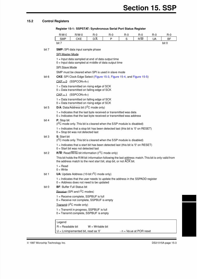
15.2 Control Registers
Register 15-1: SSPSTAT: Synchronous Serial Port Status Register
R/W-0 R/W-0 R-0 R-0 R-0 R-0 R-0 R-0
SMP CKE D/A P S R/W UA BF
bit 7 bit 0
bit 7 SMP: SPI data input sample phase
SPI Master Mode
1 = Input data sampled at end of data output time
0 = Input data sampled at middle of data output time
SPI Slave Mode
SMP must be cleared when SPI is used in slave mode
bit 6 CKE: SPI Clock Edge Select (Figure 15-3, Figure 15-4, and Figure 15-5)
CKP = 0 (SSPCON<4>)
1 = Data transmitted on rising edge of SCK
0 = Data transmitted on falling edge of SCK
CKP = 1 (SSPCON<4>)
1 = Data transmitted on falling edge of SCK
0 = Data transmitted on rising edge of SCK
bit 5 D/A: Data/Address bit (I2C mode only)
1 = Indicates that the last byte received or transmitted was data
0 = Indicates that the last byte received or transmitted was address
bit 4 P: Stop bit
(I2C mode only. This bit is cleared when the SSP module is disabled)
1 = Indicates that a stop bit has been detected last (this bit is '0' on RESET)
0 = Stop bit was not detected last
bit 3 S: Start bit
(I2C mode only. This bit is cleared when the SSP module is disabled)
1 = Indicates that a start bit has been detected last (this bit is '0' on RESET)
0 = Start bit was not detected last
bit 2 R/W: Read/Write bit information (I2C mode only)
This bit holds the R/W bit information following the last address match. This bit is only valid from
the address match to the next start bit, stop bit, or not ACK bit.
1 = Read
0 = Write
bit 1 UA: Update Address (10-bit I2C mode only)
1 = Indicates that the user needs to update the address in the SSPADD register
0 = Address does not need to be updated
bit 0 BF: Buffer Full Status bit
Receive (SPI and I2C modes)
1 = Receive complete, SSPBUF is full0 = Receive not complete, SSPBUF is empty
Transmit (I2C mode only)
1 = Transmit in progress, SSPBUF is full
0 = Transmit complete, SSPBUF is empty
Legend
R = Readable bit W = Writable bit
U = Unimplemented bit, read as ‘0’ - n = Value at POR reset
8/6/2019 Section 15. Synchronous Serial Port (SSP)
http://slidepdf.com/reader/full/section-15-synchronous-serial-port-ssp 4/30
PICmicro MID-RANGE MCU FAMILY
DS31015A-page 15-4 © 1997 Microchip Technology Inc.
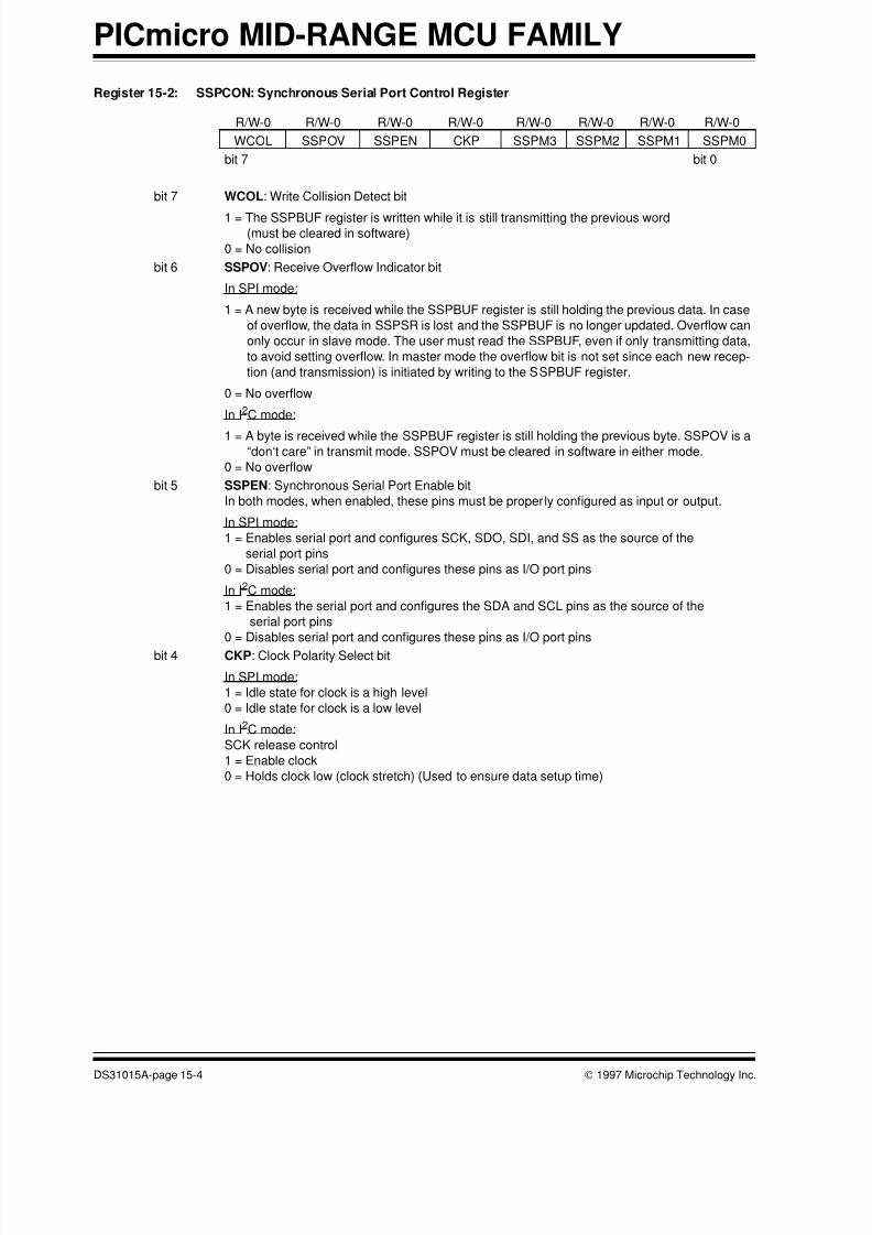
Register 15-2: SSPCON: Synchronous Serial Port Control Register
R/W-0 R/W-0 R/W-0 R/W-0 R/W-0 R/W-0 R/W-0 R/W-0
WCOL SSPOV SSPEN CKP SSPM3 SSPM2 SSPM1 SSPM0
bit 7 bit 0
bit 7 WCOL: Write Collision Detect bit
1 = The SSPBUF register is written while it is still transmitting the previous word(must be cleared in software)
0 = No collision
bit 6 SSPOV: Receive Overflow Indicator bit
In SPI mode:
1 = A new byte is received while the SSPBUF register is still holding the previous data. In case
of overflow, the data in SSPSR is lost and the SSPBUF is no longer updated. Overflow can
only occur in slave mode. The user must read the SSPBUF, even if only transmitting data,
to avoid setting overflow. In master mode the overflow bit is not set since each new recep-
tion (and transmission) is initiated by writing to the SSPBUF register.
0 = No overflow
In I2C mode:
1 = A byte is received while the SSPBUF register is still holding the previous byte. SSPOV is a“don‘t care” in transmit mode. SSPOV must be cleared in software in either mode.
0 = No overflow
bit 5 SSPEN: Synchronous Serial Port Enable bit
In both modes, when enabled, these pins must be properly configured as input or output.
In SPI mode:
1 = Enables serial port and configures SCK, SDO, SDI, and SS as the source of the
serial port pins
0 = Disables serial port and configures these pins as I/O port pins
In I2C mode:
1 = Enables the serial port and configures the SDA and SCL pins as the source of the
serial port pins
0 = Disables serial port and configures these pins as I/O port pins
bit 4 CKP: Clock Polarity Select bit
In SPI mode:
1 = Idle state for clock is a high level
0 = Idle state for clock is a low level
In I2C mode:
SCK release control
1 = Enable clock
0 = Holds clock low (clock stretch) (Used to ensure data setup time)
8/6/2019 Section 15. Synchronous Serial Port (SSP)
http://slidepdf.com/reader/full/section-15-synchronous-serial-port-ssp 5/30
© 1997 Microchip Technology Inc. DS31015A-page 15-5
Section 15. SSP
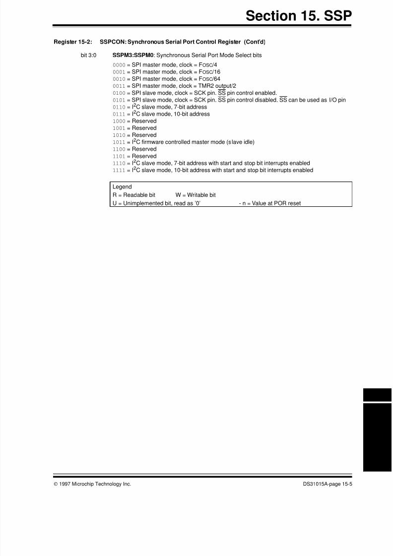
bit 3:0 SSPM3:SSPM0: Synchronous Serial Port Mode Select bits
0000 = SPI master mode, clock = FOSC /4
0001 = SPI master mode, clock = FOSC /16
0010 = SPI master mode, clock = FOSC /64
0011 = SPI master mode, clock = TMR2 output/2
0100 = SPI slave mode, clock = SCK pin. SS pin control enabled.
0101 = SPI slave mode, clock = SCK pin. SS pin control disabled. SS can be used as I/O pin
0110 = I2C slave mode, 7-bit address
0111 = I2C slave mode, 10-bit address
1000 = Reserved
1001 = Reserved
1010 = Reserved
1011 = I2C firmware controlled master mode (slave idle)
1100 = Reserved
1101 = Reserved
1110 = I2C slave mode, 7-bit address with start and stop bit interrupts enabled
1111 = I2C slave mode, 10-bit address with start and stop bit interrupts enabled
Legend
R = Readable bit W = Writable bitU = Unimplemented bit, read as ’0’ - n = Value at POR reset
Register 15-2: SSPCON: Synchronous Serial Port Control Register (Cont’d)
8/6/2019 Section 15. Synchronous Serial Port (SSP)
http://slidepdf.com/reader/full/section-15-synchronous-serial-port-ssp 6/30
PICmicro MID-RANGE MCU FAMILY
DS31015A-page 15-6 © 1997 Microchip Technology Inc.
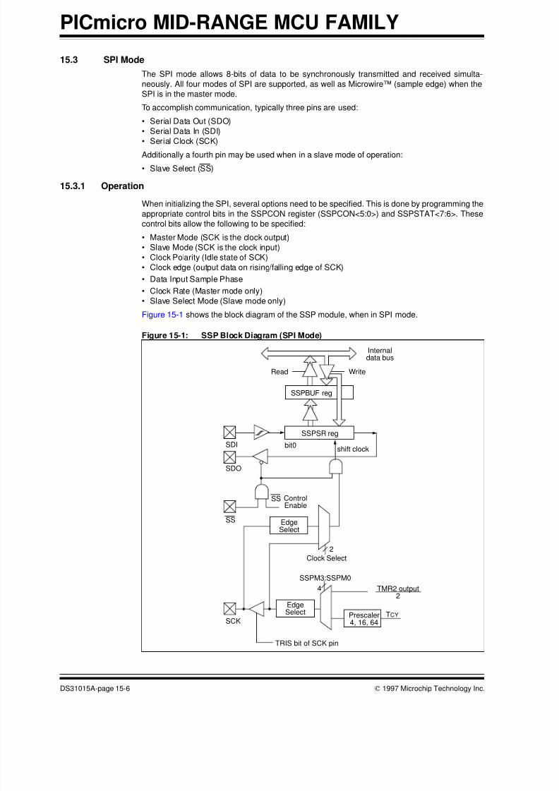
15.3 SPI Mode
The SPI mode allows 8-bits of data to be synchronously transmitted and received simulta-
neously. All four modes of SPI are supported, as well as Microwire™ (sample edge) when the
SPI is in the master mode.
To accomplish communication, typically three pins are used:
• Serial Data Out (SDO)
• Serial Data In (SDI)
• Serial Clock (SCK)
Additionally a fourth pin may be used when in a slave mode of operation:
• Slave Select (SS)
15.3.1 Operation
When initializing the SPI, several options need to be specified. This is done by programming the
appropriate control bits in the SSPCON register (SSPCON<5:0>) and SSPSTAT<7:6>. These
control bits allow the following to be specified:
• Master Mode (SCK is the clock output)
• Slave Mode (SCK is the clock input)
• Clock Polarity (Idle state of SCK)
• Clock edge (output data on rising/falling edge of SCK)
• Data Input Sample Phase
• Clock Rate (Master mode only)
• Slave Select Mode (Slave mode only)
Figure 15-1 shows the block diagram of the SSP module, when in SPI mode.
Figure 15-1: SSP Block Diagram (SPI Mode)
Read Write
Internaldata bus
SDI
SDO
SS
SCK
SSPSR reg
SSPBUF reg
SSPM3:SSPM0
bit0shift clock
SS ControlEnable
EdgeSelect
Clock Select
TMR2 output
TCYPrescaler4, 16, 64
TRIS bit of SCK pin
2
EdgeSelect
2
4
8/6/2019 Section 15. Synchronous Serial Port (SSP)
http://slidepdf.com/reader/full/section-15-synchronous-serial-port-ssp 7/30
© 1997 Microchip Technology Inc. DS31015A-page 15-7
Section 15. SSP
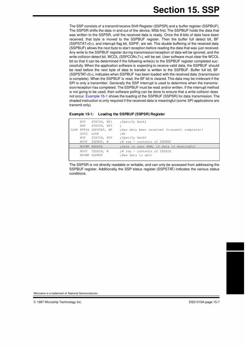
The SSP consists of a transmit/receive Shift Register (SSPSR) and a buffer register (SSPBUF).
The SSPSR shifts the data in and out of the device, MSb first. The SSPBUF holds the data that
was written to the SSPSR, until the received data is ready. Once the 8-bits of data have been
received, that byte is moved to the SSPBUF register. Then the buffer full detect bit, BF
(SSPSTAT<0>), and interrupt flag bit, SSPIF, are set. This double buffering of the received data
(SSPBUF) allows the next byte to start reception before reading the data that was just received.
Any write to the SSPBUF register during transmission/reception of data will be ignored, and the
write collision detect bit, WCOL (SSPCON<7>), will be set. User software must clear the WCOL
bit so that it can be determined if the following write(s) to the SSPBUF register completed suc-cessfully. When the application software is expecting to receive valid data, the SSPBUF should
be read before the next byte of data to transfer is written to the SSPBUF. Buffer full bit, BF
(SSPSTAT<0>), indicates when SSPBUF has been loaded with the received data (transmission
is complete). When the SSPBUF is read, the BF bit is cleared. This data may be irrelevant if the
SPI is only a transmitter. Generally the SSP Interrupt is used to determine when the transmis-
sion/reception has completed. The SSPBUF must be read and/or written. If the interrupt method
is not going to be used, then software polling can be done to ensure that a write collision does
not occur. Example 15-1 shows the loading of the SSPBUF (SSPSR) for data transmission. The
shaded instruction is only required if the received data is meaningful (some SPI applications are
transmit only).
Example 15-1: Loading the SSPBUF (SSPSR) Register
The SSPSR is not directly readable or writable, and can only be accessed from addressing the
SSPBUF register. Additionally, the SSP status register (SSPSTAT) indicates the various status
conditions.
BCF STATUS, RP1 ;Specify Bank1BSF STATUS, RP0 ;
LOOP BTFSS SSPSTAT, BF ;Has data been received (transmit complete)?
GOTO LOOP ;No
BCF STATUS, RP0 ;Specify Bank0
MOVF SSPBUF, W ;W reg = contents of SSPBUF
MOVWF RXDATA ;Save in user RAM, if data is meaningful
MOVF TXDATA, W ;W reg = contents of TXDATA
MOVWF SSPBUF ;New data to xmit
Microwire is a trademark of National Semiconductor.
8/6/2019 Section 15. Synchronous Serial Port (SSP)
http://slidepdf.com/reader/full/section-15-synchronous-serial-port-ssp 8/30
PICmicro MID-RANGE MCU FAMILY
DS31015A-page 15-8 © 1997 Microchip Technology Inc.
15.3.2 Enabling SPI I/O
To enable the serial port the SSP Enable bit, SSPEN (SSPCON<5>), must be set. To reset or
reconfigure SPI mode, clear the SSPEN bit which re-initializes the SSPCON register, and then
set the SSPEN bit. This configures the SDI, SDO, SCK, and SS pins as serial port pins. For the
pins to behave as the serial port function, they must have their data direction bits (in the TRIS
register) appropriately programmed. That is:
• SDI must have the TRIS bit set
• SDO must have the TRIS bit cleared
• SCK (Master mode) must have the TRIS bit cleared
• SCK (Slave mode) must have the TRIS bit set
• SS must have the TRIS bit set
Any serial port function that is not desired may be overridden by programming the corresponding
data direction (TRIS) register to the opposite value. An example would be in master mode where
you are only sending data (to a display driver), then both SDI and SS could be used as general
purpose outputs by clearing their corresponding TRIS register bits.
8/6/2019 Section 15. Synchronous Serial Port (SSP)
http://slidepdf.com/reader/full/section-15-synchronous-serial-port-ssp 9/30
© 1997 Microchip Technology Inc. DS31015A-page 15-9
Section 15. SSP
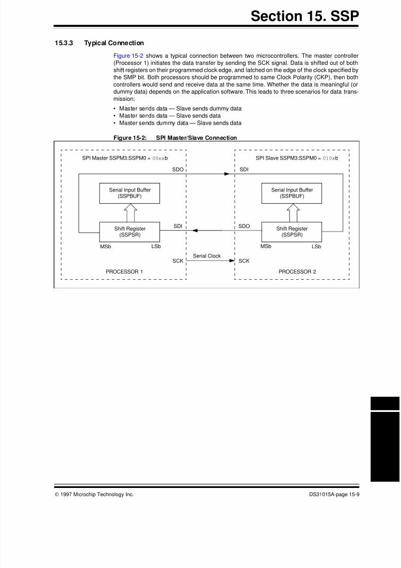
15.3.3 Typical Connection
Figure 15-2 shows a typical connection between two microcontrollers. The master controller
(Processor 1) initiates the data transfer by sending the SCK signal. Data is shifted out of both
shift registers on their programmed clock edge, and latched on the edge of the clock specified by
the SMP bit. Both processors should be programmed to same Clock Polarity (CKP), then both
controllers would send and receive data at the same time. Whether the data is meaningful (or
dummy data) depends on the application software. This leads to three scenarios for data trans-
mission:• Master sends data — Slave sends dummy data
• Master sends data — Slave sends data
• Master sends dummy data — Slave sends data
Figure 15-2: SPI Master/Slave Connection
Serial Input Buffer(SSPBUF)
Shift Register(SSPSR)
MSb LSb
SDO
SDI
PROCESSOR 1
SCK
SPI Master SSPM3:SSPM0 = 00xxb
Serial Input Buffer(SSPBUF)
Shift Register(SSPSR)
LSbMSb
SDI
SDO
PROCESSOR 2
SCK
SPI Slave SSPM3:SSPM0 = 010xb
Serial Clock
8/6/2019 Section 15. Synchronous Serial Port (SSP)
http://slidepdf.com/reader/full/section-15-synchronous-serial-port-ssp 10/30
PICmicro MID-RANGE MCU FAMILY
DS31015A-page 15-10 © 1997 Microchip Technology Inc.
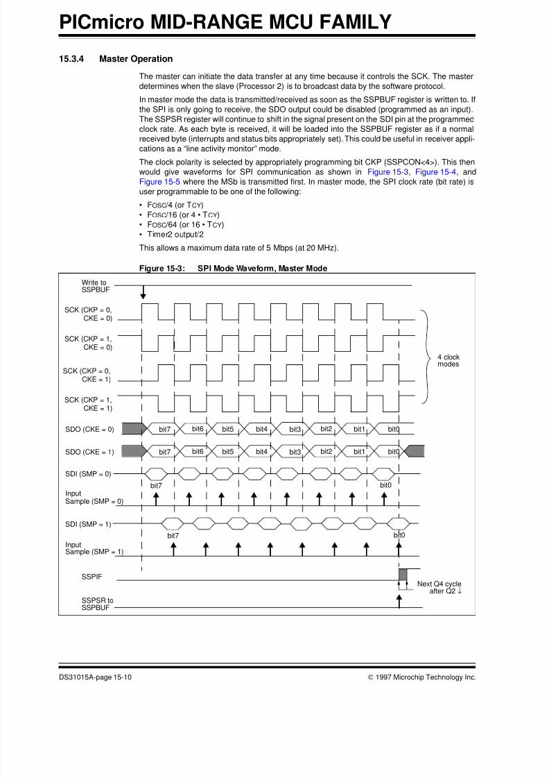
15.3.4 Master Operation
The master can initiate the data transfer at any time because it controls the SCK. The master
determines when the slave (Processor 2) is to broadcast data by the software protocol.
In master mode the data is transmitted/received as soon as the SSPBUF register is written to. If
the SPI is only going to receive, the SDO output could be disabled (programmed as an input).
The SSPSR register will continue to shift in the signal present on the SDI pin at the programmed
clock rate. As each byte is received, it will be loaded into the SSPBUF register as if a normal
received byte (interrupts and status bits appropriately set). This could be useful in receiver appli-cations as a “line activity monitor” mode.
The clock polarity is selected by appropriately programming bit CKP (SSPCON<4>). This then
would give waveforms for SPI communication as shown in Figure 15-3, Figure 15-4, and
Figure 15-5 where the MSb is transmitted first. In master mode, the SPI clock rate (bit rate) is
user programmable to be one of the following:
• FOSC /4 (or TCY)
• FOSC /16 (or 4 • TCY)
• FOSC /64 (or 16 • TCY)
• Timer2 output/2
This allows a maximum data rate of 5 Mbps (at 20 MHz).
Figure 15-3: SPI Mode Waveform, Master Mode
4 clockmodes
InputSample (SMP = 0)
InputSample (SMP = 1)
SDI (SMP = 0)
bit7 bit0
SDO (CKE = 0) bit7 bit6 bit5 bit4 bit3 bit2 bit1 bit0
bit7 bit0
SDI (SMP = 1)
SSPIF
Write toSSPBUF
SSPSR toSSPBUF
SDO (CKE = 1) bit7 bit6 bit5 bit4 bit3 bit2 bit1 bit0
SCK (CKP = 0,CKE = 0)
SCK (CKP = 0,CKE = 1)
SCK (CKP = 1,CKE = 0)
SCK (CKP = 1,
CKE = 1)
Next Q4 cycleafter Q2 ↓
8/6/2019 Section 15. Synchronous Serial Port (SSP)
http://slidepdf.com/reader/full/section-15-synchronous-serial-port-ssp 11/30
© 1997 Microchip Technology Inc. DS31015A-page 15-11
Section 15. SSP
15.3.5 Slave Operation
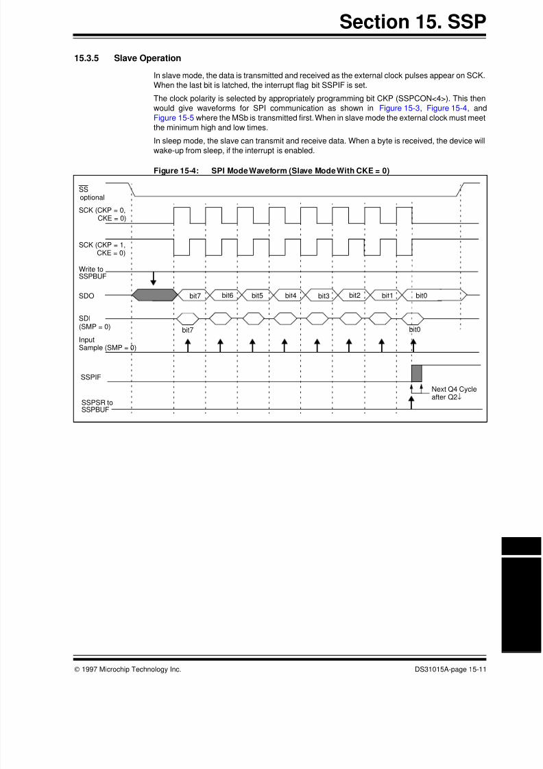
In slave mode, the data is transmitted and received as the external clock pulses appear on SCK.
When the last bit is latched, the interrupt flag bit SSPIF is set.
The clock polarity is selected by appropriately programming bit CKP (SSPCON<4>). This then
would give waveforms for SPI communication as shown in Figure 15-3, Figure 15-4, and
Figure 15-5 where the MSb is transmitted first. When in slave mode the external clock must meet
the minimum high and low times.
In sleep mode, the slave can transmit and receive data. When a byte is received, the device will
wake-up from sleep, if the interrupt is enabled.
Figure 15-4: SPI Mode Waveform (Slave Mode With CKE = 0)
SCK (CKP = 1,
SCK (CKP = 0,
InputSample (SMP = 0)
SDI
bit7 bit0
SDO bit6 bit5 bit4 bit3 bit2 bit1 bit0
SSPIF
CKE = 0)
CKE = 0)
(SMP = 0)
Write toSSPBUF
SSPSR toSSPBUF
SSoptional
Next Q4 Cycleafter Q2↓
bit7
8/6/2019 Section 15. Synchronous Serial Port (SSP)
http://slidepdf.com/reader/full/section-15-synchronous-serial-port-ssp 12/30
PICmicro MID-RANGE MCU FAMILY
DS31015A-page 15-12 © 1997 Microchip Technology Inc.
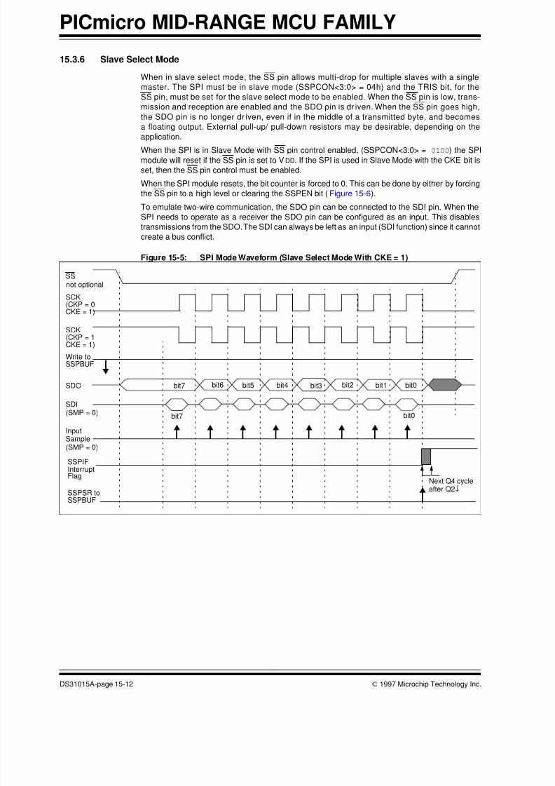
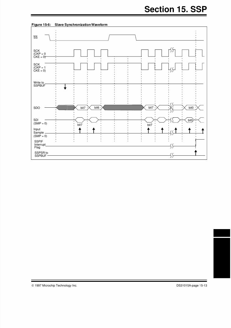
15.3.6 Slave Select Mode
When in slave select mode, the SS pin allows multi-drop for multiple slaves with a single
master. The SPI must be in slave mode (SSPCON<3:0> = 04h) and the TRIS bit, for the
SS pin, must be set for the slave select mode to be enabled. When the SS pin is low, trans-
mission and reception are enabled and the SDO pin is dr iven. When the SS pin goes high,
the SDO pin is no longer dr iven, even if in the middle of a transmitted byte, and becomes
a floating output. External pull-up/ pull-down resistors may be desirable, depending on the
application.When the SPI is in Slave Mode with SS pin control enabled, (SSPCON<3:0> = 0100) the SPI
module will reset if the SS pin is set to VDD. If the SPI is used in Slave Mode with the CKE bit is
set, then the SS pin control must be enabled.
When the SPI module resets, the bit counter is forced to 0. This can be done by either by forcing
the SS pin to a high level or clearing the SSPEN bit (Figure 15-6).
To emulate two-wire communication, the SDO pin can be connected to the SDI pin. When the
SPI needs to operate as a receiver the SDO pin can be configured as an input. This disables
transmissions from the SDO. The SDI can always be left as an input (SDI function) since it cannot
create a bus conflict.
Figure 15-5: SPI Mode Waveform (Slave Select Mode With CKE = 1)
SCK(CKP = 1
SCK(CKP = 0
InputSample
SDI
bit7 bit0
SDO bit7 bit6 bit5 bit4 bit3 bit2 bit1 bit0
SSPIFInterrupt
(SMP = 0)
CKE = 1)
CKE = 1)
(SMP = 0)
Write toSSPBUF
SSPSR toSSPBUF
SS
Flag
not optional
Next Q4 cycleafter Q2↓
8/6/2019 Section 15. Synchronous Serial Port (SSP)
http://slidepdf.com/reader/full/section-15-synchronous-serial-port-ssp 13/30
© 1997 Microchip Technology Inc. DS31015A-page 15-13
Section 15. SSP
Figure 15-6: Slave Synchronization Waveform
SCK(CKP = 1
SCK(CKP = 0
InputSample
SDI
bit7
SDO bit7 bit6 bit7
SSPIFInterrupt
(SMP = 0)
CKE = 0)
CKE = 0)
(SMP = 0)
Write toSSPBUF
SSPSR toSSPBUF
SS
Flag
bit0
bit7
bit0
8/6/2019 Section 15. Synchronous Serial Port (SSP)
http://slidepdf.com/reader/full/section-15-synchronous-serial-port-ssp 14/30
PICmicro MID-RANGE MCU FAMILY
DS31015A-page 15-14 © 1997 Microchip Technology Inc.
15.3.7 Sleep Operation
In master mode all module clocks are halted, and the transmission/reception will remain in that
state until the device wakes from sleep. After the device returns to normal mode, the module will
continue to transmit/receive data.
In slave mode, the SPI transmit/receive shift register operates asynchronously to the device. This
allows the device to be placed in sleep mode, and data to be shifted into the SPI transmit/receive
shift register. When all 8-bits have been received, the SSP interrupt flag bit will be set and if
enabled will wake the device from sleep.

8/6/2019 Section 15. Synchronous Serial Port (SSP)
http://slidepdf.com/reader/full/section-15-synchronous-serial-port-ssp 15/30
© 1997 Microchip Technology Inc. DS31015A-page 15-15
Section 15. SSP
15.3.8 Effects of a Reset
A reset disables the SSP module and terminates the current transfer.
Table 15-1: Registers Associated with SPI Operation
Name Bit 7 Bit 6 Bit 5 Bit 4 Bit 3 Bit 2 Bit 1 Bit 0
Value on
POR,
BOR
Value on all
other resets
INTCON GIE PEIE T0IE INTE RBIE(2) T0IF INTF RBIF(2) 0000 000x 0000 000u
PIR SSPIF (1) 0 0
PIE SSPIE (1) 0 0
SSPBUF Synchronous Serial Port Receive Buffer/Transmit Register xxxx xxxx uuuu uuuu
SSPCON WCOL SSPOV SSPEN CKP SSPM3 SSPM2 SSPM1 SSPM0 0000 0000 0000 0000
TRISA — — PORTA Data Direction Register --11 1111 --11 1111
TRISC PORTC Data Direction Control Register 1111 1111 1111 1111
SSPSTAT SMP CKE D/A P S R/W UA BF 0000 0000 0000 0000
Legend: x = unknown, u = unchanged, - = unimplemented read as '0'. Shaded cells are not used by the SSP in SPI
mode.
Note 1: The position of this bit is device dependent.2: These bits may also be named GPIE and GPIF.
8/6/2019 Section 15. Synchronous Serial Port (SSP)
http://slidepdf.com/reader/full/section-15-synchronous-serial-port-ssp 16/30
PICmicro MID-RANGE MCU FAMILY
DS31015A-page 15-16 © 1997 Microchip Technology Inc.
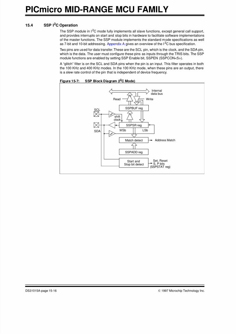
15.4 SSP I2C Operation
The SSP module in I2C mode fully implements all slave functions, except general call support,
and provides interrupts on start and stop bits in hardware to facilitate software implementations
of the master functions. The SSP module implements the standard mode specifications as well
as 7-bit and 10-bit addressing. Appendix A gives an overview of the I2C bus specification.
Two pins are used for data transfer. These are the SCL pin, which is the clock, and the SDA pin,
which is the data. The user must configure these pins as inputs through the TRIS bits. The SSP
module functions are enabled by setting SSP Enable bit, SSPEN (SSPCON<5>).A “glitch” filter is on the SCL and SDA pins when the pin is an input. This filter operates in both
the 100 KHz and 400 KHz modes. In the 100 KHz mode, when these pins are an output, there
is a slew rate control of the pin that is independent of device frequency.
Figure 15-7: SSP Block Diagram (I2C Mode)
Read Write
SSPSR reg
Match detect
SSPADD reg
Start andStop bit detect
SSPBUF reg
Internaldata bus
Address Match
Set, ResetS, P bits
(SSPSTAT reg)
SCL
shiftclock
MSb LSbSDA
8/6/2019 Section 15. Synchronous Serial Port (SSP)
http://slidepdf.com/reader/full/section-15-synchronous-serial-port-ssp 17/30
© 1997 Microchip Technology Inc. DS31015A-page 15-17
Section 15. SSP
The SSP module has five registers for I2C operation. They are:
• SSP Control Register (SSPCON)
• SSP Status Register (SSPSTAT)
• Serial Receive/Transmit Buffer (SSPBUF)
• SSP Shift Register (SSPSR) - Not directly accessible
• SSP Address Register (SSPADD)
The SSPCON register allows control of the I2C operation. Four mode selection bits
(SSPCON<3:0>) allow one of the following I2
C modes to be selected:• I2C Slave mode (7-bit address)
• I2C Slave mode (10-bit address)
• I2C Firmware controlled Multi-Master mode (start and stop bit interrupts enabled)
• I2C Firmware controlled Multi-Master mode (start and stop bit interrupts enabled)
• I2C Firmware controlled Master mode, slave is idle
Before selecting any I2C mode, the SCL and SDA pins must be programmed to inputs by setting
the appropriate TRIS bits. Selecting an I 2C mode, by setting the SSPEN bit, enables the SCL
and SDA pins to be used as the clock and data lines in I 2C mode.
The SSPSTAT register gives the status of the data transfer. This information includes detection
of a START or STOP bit, specifies if the received byte was data or address, if the next byte is the
completion of 10-bit address, and if this will be a read or write data transfer.
The SSPBUF is the register to which transfer data is written to or read from. The SSPSR register
shifts the data in or out of the device. In receive operations, the SSPBUF and SSPSR create a
doubled buffered receiver. This allows reception of the next byte to begin before reading the last
byte of received data. When the complete byte is received, it is transferred to the SSPBUF reg-
ister and flag bit SSPIF is set. If another complete byte is received before the SSPBUF register
is read, a receiver overflow has occurred and the SSPOV bit (SSPCON<6>) is set and the byte
in the SSPSR is lost.
The SSPADD register holds the slave address. In 10-bit mode, the user needs to write the high
byte of the address (1111 0 A9 A8 0). Following the high byte address match, the low byte of
the address needs to be loaded (A7:A0).
8/6/2019 Section 15. Synchronous Serial Port (SSP)
http://slidepdf.com/reader/full/section-15-synchronous-serial-port-ssp 18/30
PICmicro MID-RANGE MCU FAMILY
DS31015A-page 15-18 © 1997 Microchip Technology Inc.
15.4.1 Slave Mode
In slave mode, the SCL and SDA pins must be configured as inputs (TRIS set). The SSP module
will override the input state with the output data when required (slave-transmitter).
When an address is matched or the data transfer after an address match is received, the hard-
ware automatically will generate the acknowledge (ACK) pulse, and then load the SSPBUF reg-
ister with the received value currently in the SSPSR register.
There are certain conditions that will cause the SSP module not to give this ACK pulse. Theseare if either (or both):
a) The buffer full bit, BF (SSPSTAT<0>), was set before the message completed.
b) The overflow bit, SSPOV (SSPCON<6>), was set before the message completed.
In this case, the SSPSR register value is not loaded into the SSPBUF, but the SSPIF and SSPOV
bits are set. Table 15-2 shows what happens when a data transfer byte is received, given the sta-
tus of bits BF and SSPOV. The shaded cells show the condition where user software did not prop-
erly clear the overflow condition. Flag bit BF is cleared by reading the SSPBUF register while bit
SSPOV is cleared through software.
The SCL clock input must have a minimum high and low time for proper operation. The high and
low times of the I2C specification as well as the requirement of the SSP module is shown in
Device Data Sheet electrical specifications parameters 100 and 101.
8/6/2019 Section 15. Synchronous Serial Port (SSP)
http://slidepdf.com/reader/full/section-15-synchronous-serial-port-ssp 19/30
© 1997 Microchip Technology Inc. DS31015A-page 15-19
Section 15. SSP
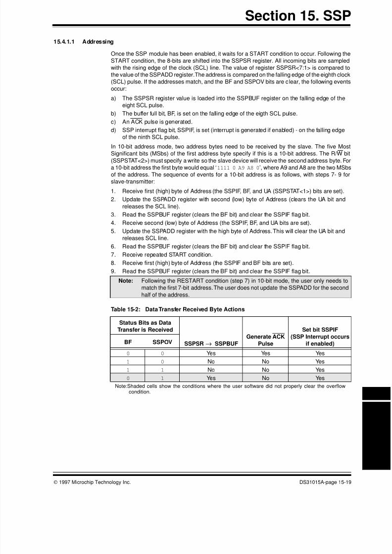
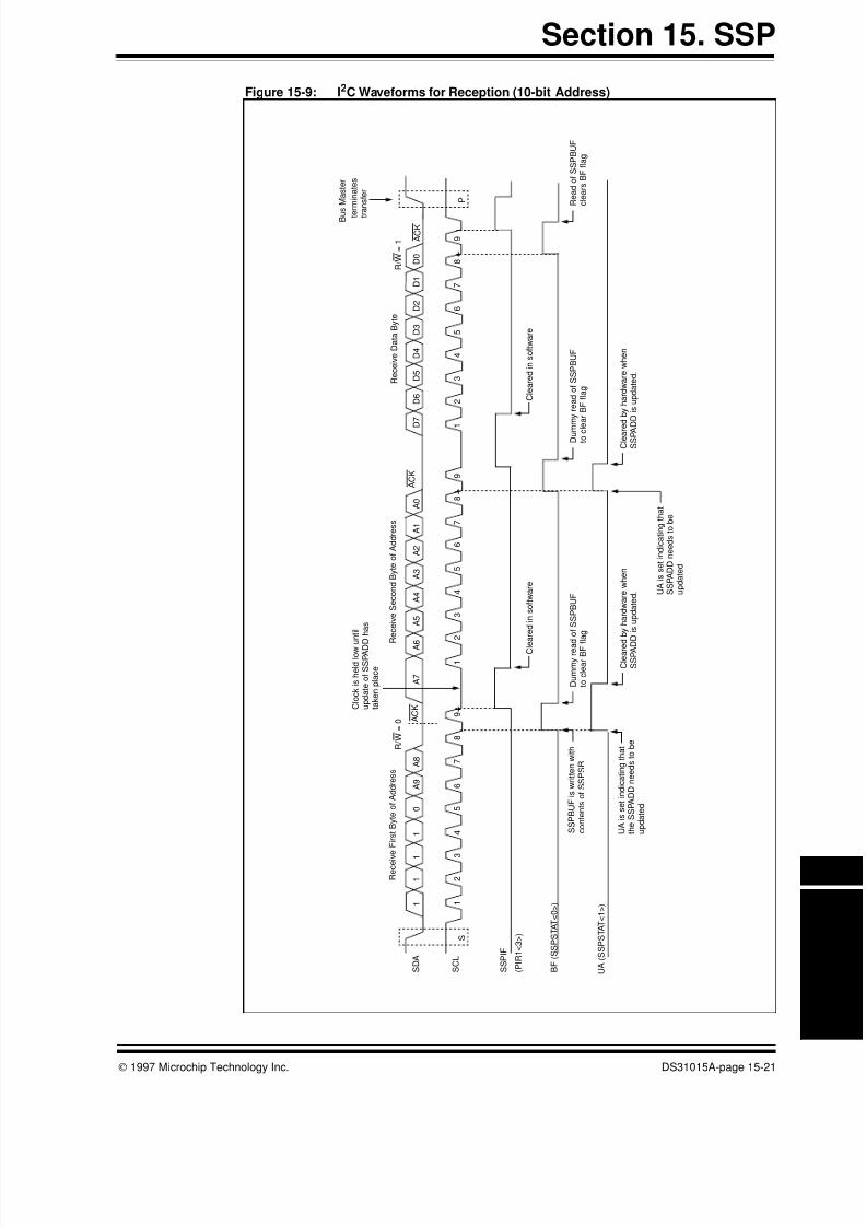
15.4.1.1 Addressing
Once the SSP module has been enabled, it waits for a START condition to occur. Following the
START condition, the 8-bits are shifted into the SSPSR register. All incoming bits are sampled
with the rising edge of the clock (SCL) line. The value of register SSPSR<7:1> is compared to
the value of the SSPADD register. The address is compared on the falling edge of the eighth clock
(SCL) pulse. If the addresses match, and the BF and SSPOV bits are clear, the following events
occur:
a) The SSPSR register value is loaded into the SSPBUF register on the falling edge of theeight SCL pulse.
b) The buffer full bit, BF, is set on the falling edge of the eigth SCL pulse.
c) An ACK pulse is generated.
d) SSP interrupt flag bit, SSPIF, is set (interrupt is generated if enabled) - on the falling edge
of the ninth SCL pulse.
In 10-bit address mode, two address bytes need to be received by the slave. The five Most
Significant bits (MSbs) of the first address byte specify if this is a 10-bit address. The R/W bit
(SSPSTAT<2>) must specify a write so the slave device will receive the second address byte. For
a 10-bit address the first byte would equal ‘1111 0 A9 A8 0’, where A9 and A8 are the two MSbs
of the address. The sequence of events for a 10-bit address is as follows, with steps 7- 9 for
slave-transmitter:
1. Receive first (high) byte of Address (the SSPIF, BF, and UA (SSPSTAT<1>) bits are set).2. Update the SSPADD register with second (low) byte of Address (clears the UA bit and
releases the SCL line).
3. Read the SSPBUF register (clears the BF bit) and clear the SSPIF flag bit.
4. Receive second (low) byte of Address (the SSPIF, BF, and UA bits are set).
5. Update the SSPADD register with the high byte of Address. This will clear the UA bit and
releases SCL line.
6. Read the SSPBUF register (clears the BF bit) and clear the SSPIF flag bit.
7. Receive repeated START condition.
8. Receive first (high) byte of Address (the SSPIF and BF bits are set).
9. Read the SSPBUF register (clears the BF bit) and clear the SSPIF flag bit.
Table 15-2: Data Transfer Received Byte Actions
Note: Following the RESTART condition (step 7) in 10-bit mode, the user only needs to
match the first 7-bit address. The user does not update the SSPADD for the second
half of the address.
Status Bits as Data
Transfer is Received
SSPSR → SSPBUF
Generate ACK
Pulse
Set bit SSPIF
(SSP Interrupt occurs
if enabled)BF SSPOV
0 0 Yes Yes Yes
1 0 No No Yes
1 1 No No Yes
0 1 Yes No Yes
Note:Shaded cells show the conditions where the user software did not properly clear the overflowcondition.
8/6/2019 Section 15. Synchronous Serial Port (SSP)
http://slidepdf.com/reader/full/section-15-synchronous-serial-port-ssp 20/30
PICmicro MID-RANGE MCU FAMILY
DS31015A-page 15-20 © 1997 Microchip Technology Inc.
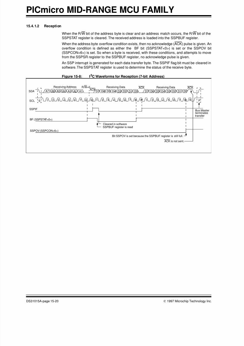
15.4.1.2 Reception
When the R/W bit of the address byte is clear and an address match occurs, the R/W bit of the
SSPSTAT register is cleared. The received address is loaded into the SSPBUF register.
When the address byte overflow condition exists, then no acknowledge (ACK) pulse is given. An
overflow condition is defined as either the BF bit (SSPSTAT<0>) is set or the SSPOV bit
(SSPCON<6>) is set. So when a byte is received, with these conditions, and attempts to move
from the SSPSR register to the SSPBUF register, no acknowledge pulse is given.
An SSP interrupt is generated for each data transfer byte. The SSPIF flag bit must be cleared in
software. The SSPSTAT register is used to determine the status of the receive byte.
Figure 15-8: I2C Waveforms for Reception (7-bit Address)
P98765
D0D1D2D3D4D5D6D7
S
A7 A6 A5 A4 A3 A2 A1SDA
SCL 1 2 3 4 5 6 7 8 9 1 2 3 4 5 6 7 8 9 1 2 3 4
Bus Masterterminatestransfer
Bit SSPOV is set because the SSPBUF register is still full.
Cleared in softwareSSPBUF register is read
ACK Receiving DataReceiving Data
D0D1D2D3D4D5D6D7ACK
R/W=0Receiving Address
SSPIF
BF (SSPSTAT<0>)
SSPOV (SSPCON<6>)
ACK
ACK is not sent.
8/6/2019 Section 15. Synchronous Serial Port (SSP)
http://slidepdf.com/reader/full/section-15-synchronous-serial-port-ssp 21/30
© 1997 Microchip Technology Inc. DS31015A-page 15-21
Section 15. SSP
Figure 15-9: I2C Waveforms for Reception (10-bit Address)
S D A
S C L
S S P I F
B F ( S S P S T A T < 0 > )
S
1
2
3
4
5
6
7
8
9
1
2
3
4
5
6
7
8
9
1
2
3
4
5
7
8
9
P
1
1
1
1
0
A 9
A 8
A 7
A 6
A 5
A 4
A 3
A 2
A 1
A 0
D 7
D 6
D 5
D 4
D 3
D 1
D 0
R e c e i v e D a t a B y t e
A C K
R / W =
0 A C K
R e c e i v e F i r s t B y t e o f A d d r e s s
C l e
a r e d i n s o f t w a r e
B u
s M a s t e r
t e
r m i n a t e s
t r a n s f e r
D 2
6
( P I R 1 < 3 > )
R e c e i v e S e c o n d B y t e o f A d d r e s s
C l e a r e d b y h a r d w a r e w h e n
S S P A D
D i s u p d a t e d .
U A ( S S P S T A T < 1 > )
C l o c k i s h e l d l o w u
n t i l
u p d a t e o f S S P A D D h a s
t a k e n p l a c e
U A i s s e t i n d i c a t i n g t h a t
t h e S S P A D D n e e d s t o b e
u p d a t e d
U A i s s e t i n d i c a t i n g t h a t
S S P A D D n e e d s t o b e
u p d a t e d
S S P B U F i s w r i t t e n w i t h
c o n t e n t s o f S S P S R
D u m m y r e a d o f S S P B U F
t o c l e a r B F fl a g
A C K
R / W =
1
C l e a r e d i n s o f t w a r e
D u m
m y r e a d o f S S P B U F
t o c l e a r B F fl a g
R e a d o f S S P B U F
c l e a r s B F fl a g
C l e a r e d b y h a r d w a r e w h e n
S S P A
D D i s u p d a t e d .
8/6/2019 Section 15. Synchronous Serial Port (SSP)
http://slidepdf.com/reader/full/section-15-synchronous-serial-port-ssp 22/30
PICmicro MID-RANGE MCU FAMILY
DS31015A-page 15-22 © 1997 Microchip Technology Inc.
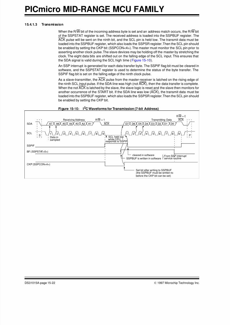
15.4.1.3 Transmission
When the R/W bit of the incoming address byte is set and an address match occurs, the R/W bit
of the SSPSTAT register is set. The received address is loaded into the SSPBUF register. The
ACK pulse will be sent on the ninth bit, and the SCL pin is held low. The transmit data must be
loaded into the SSPBUF register, which also loads the SSPSR register. Then the SCL pin should
be enabled by setting the CKP bit (SSPCON<4>). The master must monitor the SCL pin prior to
asserting another clock pulse. The slave devices may be holding off the master by stretching the
clock. The eight data bits are shifted out on the falling edge of the SCL input. This ensures thatthe SDA signal is valid during the SCL high time (Figure 15-10).
An SSP interrupt is generated for each data transfer byte. The SSPIF flag bit must be cleared in
software, and the SSPSTAT register is used to determine the status of the byte transfer. The
SSPIF flag bit is set on the falling edge of the ninth clock pulse.
As a slave-transmitter, the ACK pulse from the master-receiver is latched on the rising edge of
the ninth SCL input pulse. If the SDA line was high (not ACK), then the data transfer is complete.
When the not ACK is latched by the slave, the slave logic is reset and the slave then monitors for
another occurrence of the START bit. If the SDA line was low (ACK), the transmit data must be
loaded into the SSPBUF register, which also loads the SSPSR register. Then the SCL pin should
be enabled by setting the CKP bit.
Figure 15-10: I2C Waveforms for Transmission (7-bit Address)
SDA
SCL
SSPIF
BF (SSPSTAT<0>)
CKP (SSPCON<4>)
A7 A6 A5 A4 A3 A2 A1 ACK D7 D6 D5 D4 D3 D2 D1 D0
ACKTransmitting DataR/W = 1Receiving Address
1 2 3 4 5 6 7 8 9 1 2 3 4 5 6 7 8 9P
cleared in software
SSPBUF is written in softwareFrom SSP interruptservice routine
Set bit after writing to SSPBUF
SData insampled
SCL held lowwhile CPU
responds to SSPIF
(the SSPBUF must be written-tobefore the CKP bit can be set)
R/W = 0

8/6/2019 Section 15. Synchronous Serial Port (SSP)
http://slidepdf.com/reader/full/section-15-synchronous-serial-port-ssp 23/30
© 1997 Microchip Technology Inc. DS31015A-page 15-23
Section 15. SSP
Figure 15-11: I2C Waveforms for Transmission (10-bit Address)
S D A
S C L
S S P I F
B F ( S S P S T A T < 0 > )
S
1
2
3
4
5
6
7
8
9
1
2
3
4
5
6
7
8
9
1
2
3
4
5
7
8
9
P
1
1
1
1
0
A 9
A 8
A 7
A 6
A 5
A 4
A 3
A 2
A 1
A 0
1
1
1
1
0
A 8
R / W = 1
A C K
A C K
R / W =
0 A C K
R e c e i v e F i r s t B y t e o f A d d r e s s
C l e a r e d i n s o f t w a r e
M a s t e r s e n d s N A C K
A 9 6
( P I R 1 < 3 > )
R e c e i v e S e c o n d B y t e o f
A d d r e s s
C l e a r e d b y h a r d w a r e w h e n
S S P A D D i s u p d a t e d .
U A ( S S P S T A T < 1 > )
C l o c k i s h e l d l o w u n t i l
u p d a t e o f S S P A D D h a s
t a k e n p l a c e
U A i s s e t
i n d i c a t i n g t h a t
t h e S S P A
D D n e e d s t o b e
u p d a t e d
U A i s s e t i n d i c a t i n
g t h a t
S S P A D D n e e d s t o b e
u p d a t e d
C l e a r e d b y h a r d w a r e w h e n
S S P A D D i s u p d a t e d .
S S P B U F i s w r i t t e n w i t h
c o n t e n t s
o f S S P S R
D u m m y r e a d o f S S P B U F
t o c l e a r B F fl a g
R e c e i v e F i r s t B y t e o f A d d r e s s
1
2
3
4
5
7
8
9
D 7
D 6
D 5
D 4
D 3
D 1
A C K
D 2
6
T r a n s m i t t i n g D a t a B y t e
D
0
D u m m y r e a d o f S S P B U F
t o c l e a r B F fl a g
S r
C l e a r e d i n s o f t w a r e
W r i t e o f S S P B U F
i n i t i a t e s t r a n s m i t
C l e a r e d i n s o f t w a r e
T r a n s
m i t i s c o m p l e t e
C K P h a s t o b e s e t f o r c l o c k t o
b e r e l e a s e d
B u s M a s t e r
t e r m i n a t e s
t r a n s f e r
8/6/2019 Section 15. Synchronous Serial Port (SSP)
http://slidepdf.com/reader/full/section-15-synchronous-serial-port-ssp 24/30
PICmicro MID-RANGE MCU FAMILY
DS31015A-page 15-24 © 1997 Microchip Technology Inc.
15.4.1.4 Clock Arbitration
Clock arbitration has the SCL pin to inhibit the master device from sending the next clock pulse.
The SSP module in I2C slave mode will hold the SCL pin low when the CPU needs to respond
to the SSP interrupt (SSPIF bit is set and the CKP bit is cleared). The data that needs to be trans-
mitted will need to be written to the SSPBUF register, and then the CKP bit will need to be set to
allow the master to generate the required clocks.
15.4.2 Master Mode (Firmware)Master mode of operation is supported by interrupt generation on the detection of the START and
STOP conditions. The STOP (P) and START (S) bits are cleared from a reset or when the SSP
module is disabled. Control of the I 2C bus may be taken when the P bit is set, or the bus is idle
with both the S and P bits clear.
In master mode the SCL and SDA lines are manipulated by clearing the corresponding TRIS
bit(s). The output level is always low, irrespective of the value(s) in the PORT register. So when
transmitting data, a '1' data bit must have it’s TRIS bit set (input) and a '0' data bit must have it’s
TRIS bit cleared (output). The same scenario is true for the SCL line with the TRIS bit.
The following events will cause SSP Interrupt Flag bit, SSPIF, to be set (SSP Interrupt if enabled):
• START condition
• STOP condition
• Data transfer byte transmitted/receivedMaster mode of operation can be done with either the slave mode idle (SSPM3:SSPM0 = 1011)
or with the slave active (SSPM3:SSP0 = 1110 or 1111). When the slave modes are enabled, the
software needs to differentiate the source(s) of the interrupt.
15.4.3 Multi-Master Mode (Firmware)
In multi-Master mode, the interrupt generation on the detection of the START and STOP condi-
tions allows the determination of when the bus is free. The STOP (P) and START (S) bits are
cleared from a reset or when the SSP module is disabled. Control of the I2C bus may be taken
when the P bit (SSPSTAT<4>) is set, or the bus is idle with both the S and P bits clear. When the
bus is busy, enabling the SSP Interrupt will generate the interrupt when the STOP condition
occurs.
In Multi-Master operation, the SDA line must be monitored to see if the signal level is the
expected output level. This check only needs to be done when a high level is output. If a high levelis expected and a low level is present, the device needs to release the SDA and SCL lines (set
the TRIS bits). There are two stages where this arbitration can be lost, they are:
• Address transfer
• Data transfer
When the slave logic is enabled, the slave continues to receive. If arbitration was lost during the
address transfer stage, communication to the device may be in progress. If addressed an ACK
pulse will be generated. If arbitration was lost during the data transfer stage, the device will need
to retransfer the data at a later time.
8/6/2019 Section 15. Synchronous Serial Port (SSP)
http://slidepdf.com/reader/full/section-15-synchronous-serial-port-ssp 25/30
© 1997 Microchip Technology Inc. DS31015A-page 15-25
Section 15. SSP
15.4.4 Sleep Operation
While in sleep mode, the I2C module can receive addresses or data, and when an address match
or complete byte transfer occurs wake the processor from sleep (if the SSP interrupt is enabled).
15.4.5 Effect of a Reset
A reset disables the SSP module and terminates the current transfer.
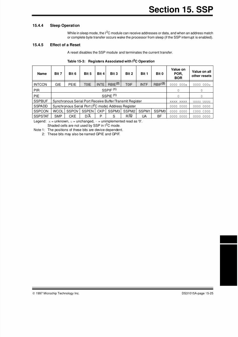
Table 15-3: Registers Associated with I2C Operation
Name Bit 7 Bit 6 Bit 5 Bit 4 Bit 3 Bit 2 Bit 1 Bit 0
Value on
POR,
BOR
Value on all
other resets
INTCON GIE PEIE T0IE INTE RBIE(2) T0IF INTF RBIF(2) 0000 000x 0000 000u
PIR SSPIF (1) 0 0
PIE SSPIE (1) 0 0
SSPBUF Synchronous Serial Port Receive Buffer/Transmit Register xxxx xxxx uuuu uuuu
SSPADD Synchronous Serial Port (I2C mode) Address Register 0000 0000 0000 0000
SSPCON WCOL SSPOV SSPEN CKP SSPM3 SSPM2 SSPM1 SSPM0 0000 0000 0000 0000
SSPSTAT SMP CKE D/A P S R/W UA BF0000 0000 0000 0000
Legend: x = unknown, u = unchanged, - = unimplemented read as '0'.
Shaded cells are not used by SSP in I2C mode.
Note 1: The positions of these bits are device dependent.
2: These bits may also be named GPIE and GPIF.
8/6/2019 Section 15. Synchronous Serial Port (SSP)
http://slidepdf.com/reader/full/section-15-synchronous-serial-port-ssp 26/30
PICmicro MID-RANGE MCU FAMILY
DS31015A-page 15-26 © 1997 Microchip Technology Inc.
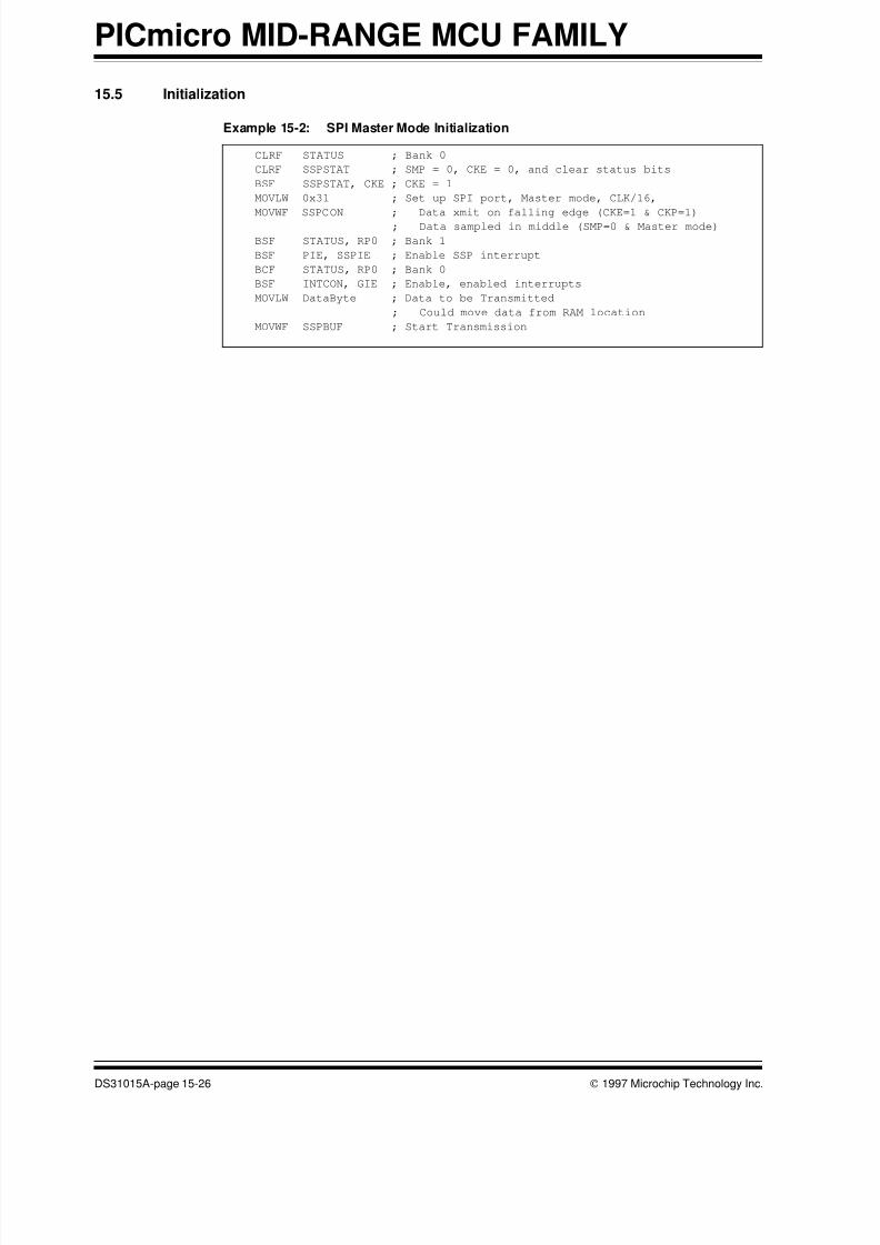
15.5 Initialization
Example 15-2: SPI Master Mode Initialization
CLRF STATUS ; Bank 0
CLRF SSPSTAT ; SMP = 0, CKE = 0, and clear status bits
BSF SSPSTAT, CKE ; CKE = 1
MOVLW 0x31 ; Set up SPI port, Master mode, CLK/16,
MOVWF SSPCON ; Data xmit on falling edge (CKE=1 & CKP=1)
; Data sampled in middle (SMP=0 & Master mode)
BSF STATUS, RP0 ; Bank 1
BSF PIE, SSPIE ; Enable SSP interrupt
BCF STATUS, RP0 ; Bank 0
BSF INTCON, GIE ; Enable, enabled interrupts
MOVLW DataByte ; Data to be Transmitted
; Could move data from RAM location
MOVWF SSPBUF ; Start Transmission
8/6/2019 Section 15. Synchronous Serial Port (SSP)
http://slidepdf.com/reader/full/section-15-synchronous-serial-port-ssp 27/30
© 1997 Microchip Technology Inc. DS31015A-page 15-27
Section 15. SSP
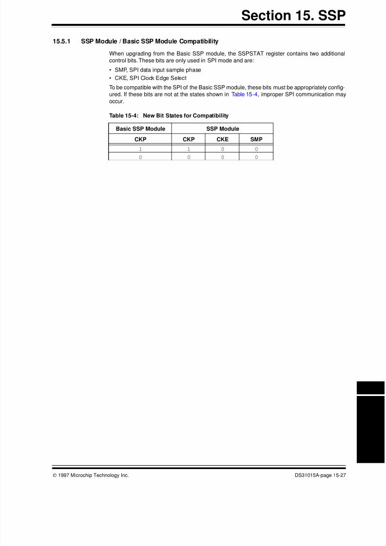
15.5.1 SSP Module / Basic SSP Module Compatibility
When upgrading from the Basic SSP module, the SSPSTAT register contains two additional
control bits. These bits are only used in SPI mode and are:
• SMP, SPI data input sample phase
• CKE, SPI Clock Edge Select
To be compatible with the SPI of the Basic SSP module, these bits must be appropriately config-
ured. If these bits are not at the states shown in Table 15-4, improper SPI communication mayoccur.
Table 15-4: New Bit States for Compatibility
Basic SSP Module SSP Module
CKP CKP CKE SMP
1 1 0 0
0 0 0 0
8/6/2019 Section 15. Synchronous Serial Port (SSP)
http://slidepdf.com/reader/full/section-15-synchronous-serial-port-ssp 28/30
PICmicro MID-RANGE MCU FAMILY
DS31015A-page 15-28 © 1997 Microchip Technology Inc.
15.6 Design Tips
Question 1: Using SPI mode, I do not seem able to talk to an SPI device.
Answer 1:
Ensure that you are using the correct SPI mode for that device. This SPI supports all four SPI
modes so you should be able to get it to function. Check the clock polarity and the clock phase.
Question 2: Using I 2 C mode, I do not seem able to make the master mode work.
Answer 2:
This SSP module does not have master mode fully automated in hardware, see Application Note
AN578 for software which uses the SSP module to implement master mode. If you require a fully
automated hardware implementation of I2C Master Mode, please refer to the Microchip Line Card
for devices that have the Master SSP module.
Question 3: Using I 2 C mode, I write data to the SSPBUF register, but the data did not
transmit.
Answer 3:
Ensure that you set the CKP bit to release the I2C clock.
Note: At the time of printing only the High-end family of devices (PIC17CXXX) have
devices with the Master SSP module implemented.

8/6/2019 Section 15. Synchronous Serial Port (SSP)
http://slidepdf.com/reader/full/section-15-synchronous-serial-port-ssp 29/30
© 1997 Microchip Technology Inc. DS31015A-page 15-29
Section 15. SSP
15.7 Related Application Notes
This section lists application notes that are related to this section of the manual. These applica-
tion notes may not be written specifically for the Mid-Range MCU family (that is they may be writ-
ten for the Base-Line, or High-End families), but the concepts are pertinent, and could be used
(with modification and possible limitations). The current application notes related to the SSP
Module are:
Title Application Note #
Use of the SSP Module in the I 2C Multi-Master Environment. AN578
Using Microchip 93 Series Serial EEPROMs with Microcontroller SPI Ports AN613
Software Implementation of I2C Bus Master AN554
Use of the SSP module in the Multi-master Environment AN578
Interfacing PIC16C64/74 to Microchip SPI Serial EEPROM AN647
Interfacing a Microchip PIC16C92x to Microchip SPI Serial EEPROM AN668
8/6/2019 Section 15. Synchronous Serial Port (SSP)
http://slidepdf.com/reader/full/section-15-synchronous-serial-port-ssp 30/30
PICmicro MID-RANGE MCU FAMILY
15.8 Revision History
Revision A
This is the initial released revision of the SSP module description.
Related Documents