August 2017 DocID029116 Rev 3 1/10 This is information on a product in full production. www.st.com DSL05 Secondary protection for VDSL2 and G.FAST lines Datasheet - production data Features High surge capability to comply with GR-1089 and ITU-T K20/21/45 Keeps peak power capability at high temperature Voltages: 8, 12, 16 and 24 V Low capacitance device: Ctyp = 0.95 pF RoHS package Low leakage current: 50 nA at 25 °C Complies with the following standards Refer to Section 2: "Schematics". Telcordia GR-1089 2.5 kV 2/10 μs - 500 A 2/10 μs AC power fault tests ITU-T K20/21/45 6 kV 10/700 μs - 150 A 5/310 μs power induction and contact tests IEC 61000-4-2, level 4 15 kV (air discharge) 8 kV (contact discharge) IEC 61000-4-5, level 2 1 kV, 42 Ω MIL STD 883G-Method 3015-7: Class 3 8 kV (human body model) Description DSL05 is designed to protect DSL line drivers against surges defined in worldwide telecommunication standards. This device protects line drivers of various systems such as xDSL and G.FAST. The low capacitance makes it suitable from ADSL to G.FAST data rates. DSL05 is able to survive severe conditions even when used with downgraded or oscillating gas tube. This device is packaged in a SOT23-6L. Figure 1: Functional diagram Table 1: Device summary Order code VRM(V) DSL05-008SC6 8 DSL05-012SC6 12 DSL05-016SC6 16 DSL05-024SC6 24 SOT23-6L NC +V LD NC I/O1 -V LD I/O2

Welcome message from author
This document is posted to help you gain knowledge. Please leave a comment to let me know what you think about it! Share it to your friends and learn new things together.
Transcript
August 2017 DocID029116 Rev 3 1/10
This is information on a product in full production. www.st.com
DSL05
Secondary protection for VDSL2 and G.FAST lines
Datasheet - production data
Features High surge capability to comply with
GR-1089 and ITU-T K20/21/45
Keeps peak power capability at high temperature
Voltages: 8, 12, 16 and 24 V
Low capacitance device: Ctyp = 0.95 pF
RoHS package
Low leakage current: 50 nA at 25 °C
Complies with the following standards Refer to Section 2: "Schematics".
Telcordia GR-1089
2.5 kV 2/10 μs - 500 A 2/10 μs
AC power fault tests
ITU-T K20/21/45
6 kV 10/700 μs - 150 A 5/310 μs
power induction and contact tests
IEC 61000-4-2, level 4
15 kV (air discharge)
8 kV (contact discharge)
IEC 61000-4-5, level 2
1 kV, 42 Ω
MIL STD 883G-Method 3015-7: Class 3
8 kV (human body model)
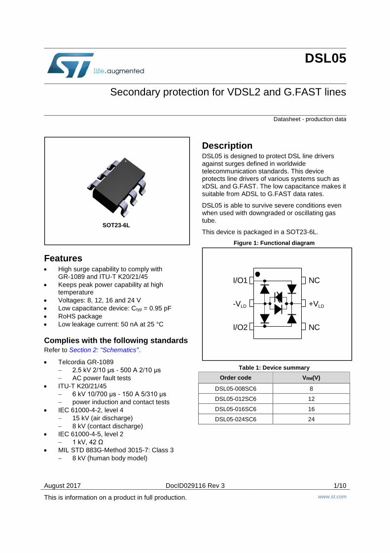
Description DSL05 is designed to protect DSL line drivers against surges defined in worldwide telecommunication standards. This device protects line drivers of various systems such as xDSL and G.FAST. The low capacitance makes it suitable from ADSL to G.FAST data rates.
DSL05 is able to survive severe conditions even when used with downgraded or oscillating gas tube.
This device is packaged in a SOT23-6L.
Figure 1: Functional diagram
Table 1: Device summary
Order code VRM(V)
DSL05-008SC6 8
DSL05-012SC6 12
DSL05-016SC6 16
DSL05-024SC6 24
SOT23-6L
NC
+VLD
NC
I/O1
-VLD
I/O2
Characteristics DSL05
2/10 DocID029116 Rev 3
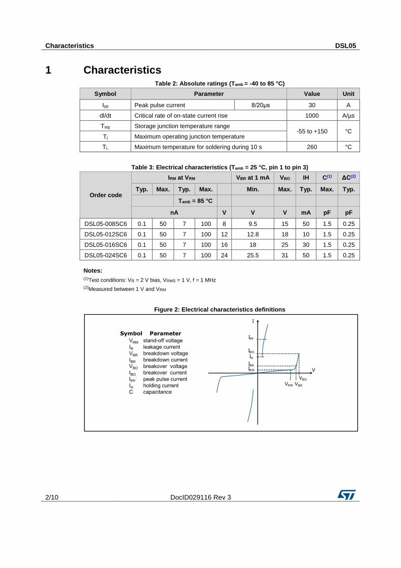
1 Characteristics Table 2: Absolute ratings (Tamb = -40 to 85 °C)
Symbol Parameter Value Unit
Ipp Peak pulse current 8/20μs 30 A
dl/dt Critical rate of on-state current rise 1000 A/µs
Tstg Storage junction temperature range -55 to +150 °C
Tj Maximum operating junction temperature
TL Maximum temperature for soldering during 10 s 260 °C
Table 3: Electrical characteristics (Tamb = 25 °C, pin 1 to pin 3)
Order code
IRM at VRM VBR at 1 mA VBO IH C(1) ΔC(2)
Typ. Max. Typ. Max.
Min. Max. Typ. Max. Typ.
Tamb = 85 °C
nA V V V mA pF pF
DSL05-008SC6 0.1 50 7 100 8 9.5 15 50 1.5 0.25
DSL05-012SC6 0.1 50 7 100 12 12.8 18 10 1.5 0.25
DSL05-016SC6 0.1 50 7 100 16 18 25 30 1.5 0.25
DSL05-024SC6 0.1 50 7 100 24 25.5 31 50 1.5 0.25
Notes:
(1)Test conditions: VR = 2 V bias, VRMS = 1 V, f = 1 MHz (2)Measured between 1 V and VRM
Figure 2: Electrical characteristics definitions
DSL05 Characteristics
DocID029116 Rev 3 3/10
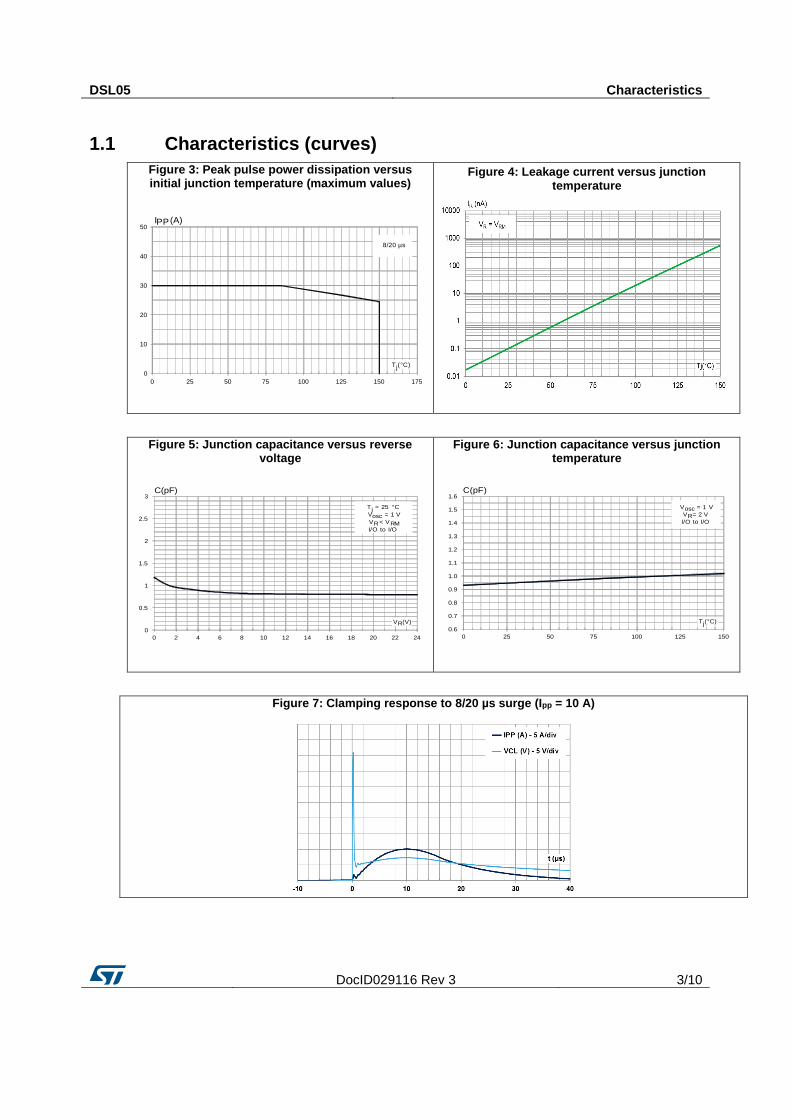
1.1 Characteristics (curves)
Figure 3: Peak pulse power dissipation versus initial junction temperature (maximum values)
Figure 4: Leakage current versus junction temperature
Figure 5: Junction capacitance versus reverse voltage
Figure 6: Junction capacitance versus junction temperature
Figure 7: Clamping response to 8/20 µs surge (Ipp = 10 A)
0
10
20
30
40
50
0 25 50 75 100 125 150 175
IPP (A)
Tj(°C)
8/20 µs
0
0.5
1
1.5
2
2.5
3
0 2 4 6 8 10 12 14 16 18 20 22 24
VR(V)
Tj = 25 °C
Vosc = 1 V
VR< VRMI/O to I/O
C(pF)
0.6
0.7
0.8
0.9
1.0
1.1
1.2
1.3
1.4
1.5
1.6
0 25 50 75 100 125 150
C(pF)
Tj(°C)
Vosc = 1 V
VR= 2 V
I/O to I/O
Schematics DSL05
4/10 DocID029116 Rev 3
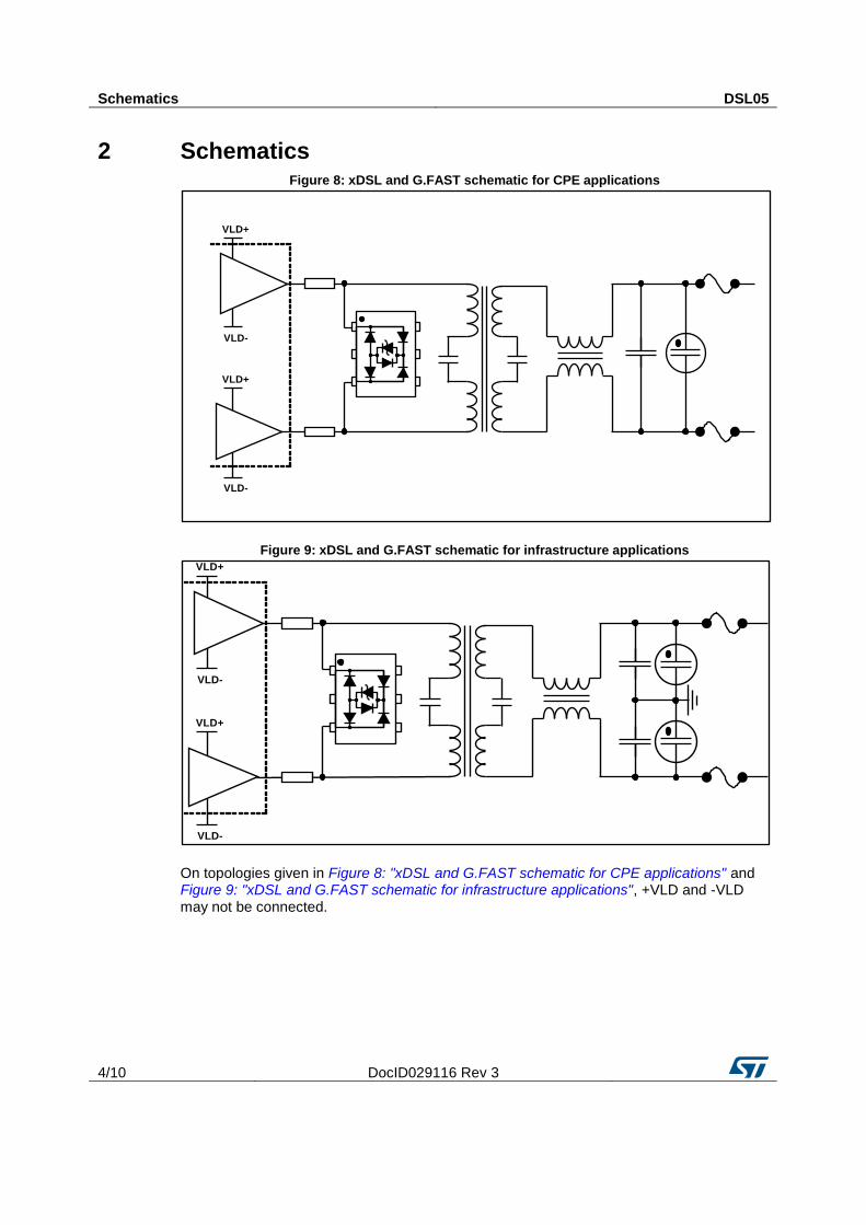
2 Schematics Figure 8: xDSL and G.FAST schematic for CPE applications
Figure 9: xDSL and G.FAST schematic for infrastructure applications
On topologies given in Figure 8: "xDSL and G.FAST schematic for CPE applications" and Figure 9: "xDSL and G.FAST schematic for infrastructure applications", +VLD and -VLD may not be connected.
VLD-
VLD+
VLD-
VLD+
VLD-
VLD+
VLD-
VLD+
DSL05 Package information
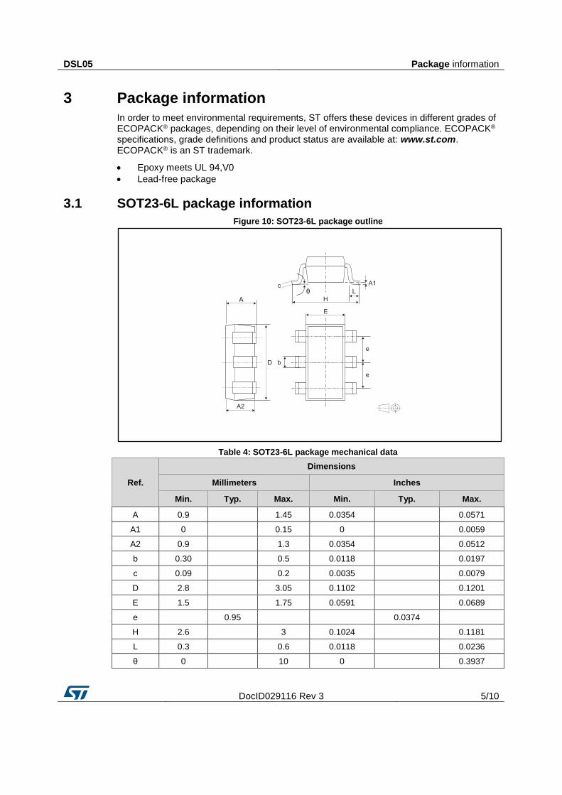
DocID029116 Rev 3 5/10
3 Package information
In order to meet environmental requirements, ST offers these devices in different grades of ECOPACK® packages, depending on their level of environmental compliance. ECOPACK® specifications, grade definitions and product status are available at: www.st.com. ECOPACK® is an ST trademark.
Epoxy meets UL 94,V0
Lead-free package
3.1 SOT23-6L package information
Figure 10: SOT23-6L package outline
Table 4: SOT23-6L package mechanical data
Ref.
Dimensions
Millimeters Inches
Min. Typ. Max. Min. Typ. Max.
A 0.9
1.45 0.0354
0.0571
A1 0
0.15 0
0.0059
A2 0.9
1.3 0.0354
0.0512
b 0.30
0.5 0.0118
0.0197
c 0.09
0.2 0.0035
0.0079
D 2.8
3.05 0.1102
0.1201
E 1.5
1.75 0.0591
0.0689
e
0.95
0.0374
H 2.6
3 0.1024
0.1181
L 0.3
0.6 0.0118
0.0236
θ 0
10 0
0.3937
Package information DSL05
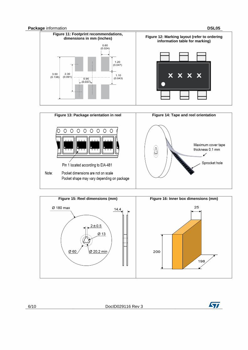
6/10 DocID029116 Rev 3
Figure 11: Footprint recommendations, dimensions in mm (inches)
Figure 12: Marking layout (refer to ordering information table for marking)
Figure 13: Package orientation in reel
Figure 14: Tape and reel orientation
Figure 15: Reel dimensions (mm)
Figure 16: Inner box dimensions (mm)
DSL05 Package information
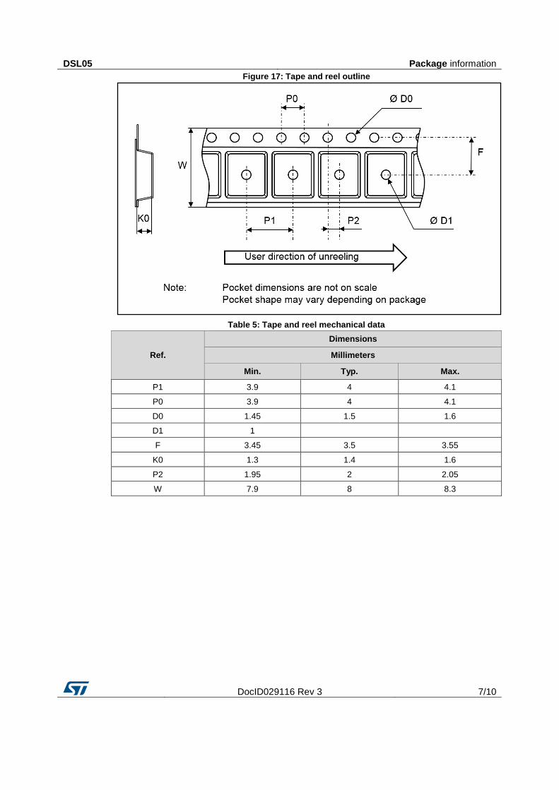
DocID029116 Rev 3 7/10
Figure 17: Tape and reel outline
Table 5: Tape and reel mechanical data
Ref.
Dimensions
Millimeters
Min. Typ. Max.
P1 3.9 4 4.1
P0 3.9 4 4.1
D0 1.45 1.5 1.6
D1 1
F 3.45 3.5 3.55
K0 1.3 1.4 1.6
P2 1.95 2 2.05
W 7.9 8 8.3
Package information DSL05
8/10 DocID029116 Rev 3
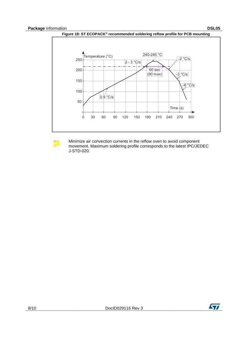
Figure 18: ST ECOPACK® recommended soldering reflow profile for PCB mounting
Minimize air convection currents in the reflow oven to avoid component movement. Maximum soldering profile corresponds to the latest IPC/JEDEC J-STD-020.
DSL05 Ordering information
DocID029116 Rev 3 9/10
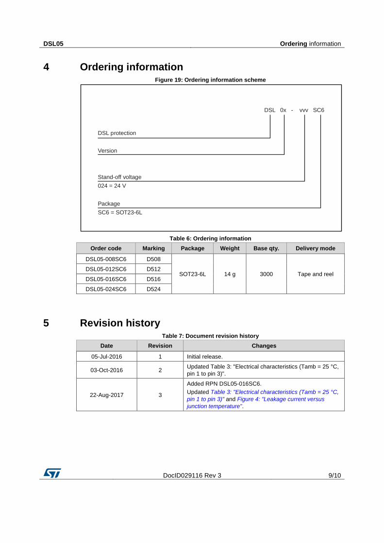
4 Ordering information Figure 19: Ordering information scheme
Table 6: Ordering information
Order code Marking Package Weight Base qty. Delivery mode
DSL05-008SC6 D508
SOT23-6L 14 g 3000 Tape and reel DSL05-012SC6 D512
DSL05-016SC6 D516
DSL05-024SC6 D524
5 Revision history Table 7: Document revision history
Date Revision Changes
05-Jul-2016 1 Initial release.
03-Oct-2016 2 Updated Table 3: "Electrical characteristics (Tamb = 25 °C,
pin 1 to pin 3)".
22-Aug-2017 3
Added RPN DSL05-016SC6.
Updated Table 3: "Electrical characteristics (Tamb = 25 °C,
pin 1 to pin 3)" and Figure 4: "Leakage current versus
junction temperature".
DSL 0x - vvv SC6
DSL protection
Version
Stand-off voltage
Package
024 = 24 V
SC6 = SOT23-6L
DSL05
10/10 DocID029116 Rev 3
IMPORTANT NOTICE – PLEASE READ CAREFULLY
STMicroelectronics NV and its subsidiaries (“ST”) reserve the right to make changes, corrections, enhancements, modifications , and improvements to ST products and/or to this document at any time without notice. Purchasers should obtain the latest relevant information on ST products before placing orders. ST products are sold pursuant to ST’s terms and conditions of sale in place at the time of order acknowledgement.
Purchasers are solely responsible for the choice, selection, and use of ST products and ST assumes no liability for application assistance or the design of Purchasers’ products.
No license, express or implied, to any intellectual property right is granted by ST herein.
Resale of ST products with provisions different from the information set forth herein shall void any warranty granted by ST for such product.
ST and the ST logo are trademarks of ST. All other product or service names are the property of their respective owners.
Information in this document supersedes and replaces information previously supplied in any prior versions of this document.
© 2017 STMicroelectronics – All rights reserved
Related Documents


![Architecture and Requirements for Fiber to the Distribution Point · 2019-05-21 · Through the use of G.fast [9] and VDSL2 [10] over short copper loops, it has become possible to](https://static.cupdf.com/doc/110x72/5f0d68617e708231d43a345c/architecture-and-requirements-for-fiber-to-the-distribution-point-2019-05-21-through.jpg)