MENA3100 - SIMS 1 Secondary ion mass spectrometry Secondary ion mass spectrometry (SIMS) (SIMS) Lasse Vines

Welcome message from author
This document is posted to help you gain knowledge. Please leave a comment to let me know what you think about it! Share it to your friends and learn new things together.
Transcript
MEN
A3100 -
SIM
S
1
Secondary ion mass spectrometrySecondary ion mass spectrometry (SIMS)(SIMS)
Lasse
Vines
MEN
A3100 -
SIM
S
2
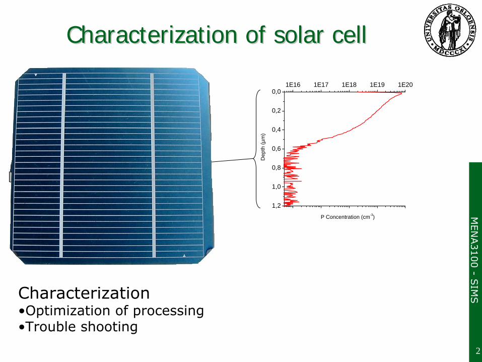
Characterization of solar cellCharacterization of solar cell
Characterization•Optimization of processing•Trouble shooting
1,2
1,0
0,8
0,6
0,4
0,2
0,01E16 1E17 1E18 1E19 1E20
Dep
th (µ
m)
P Concentration (cm-3)
MEN
A3100 -
SIM
S
3
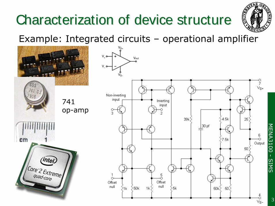
Characterization of device structureCharacterization of device structureExample: Integrated circuits –
operational amplifier
741
op-amp
MEN
A3100 -
SIM
S
4
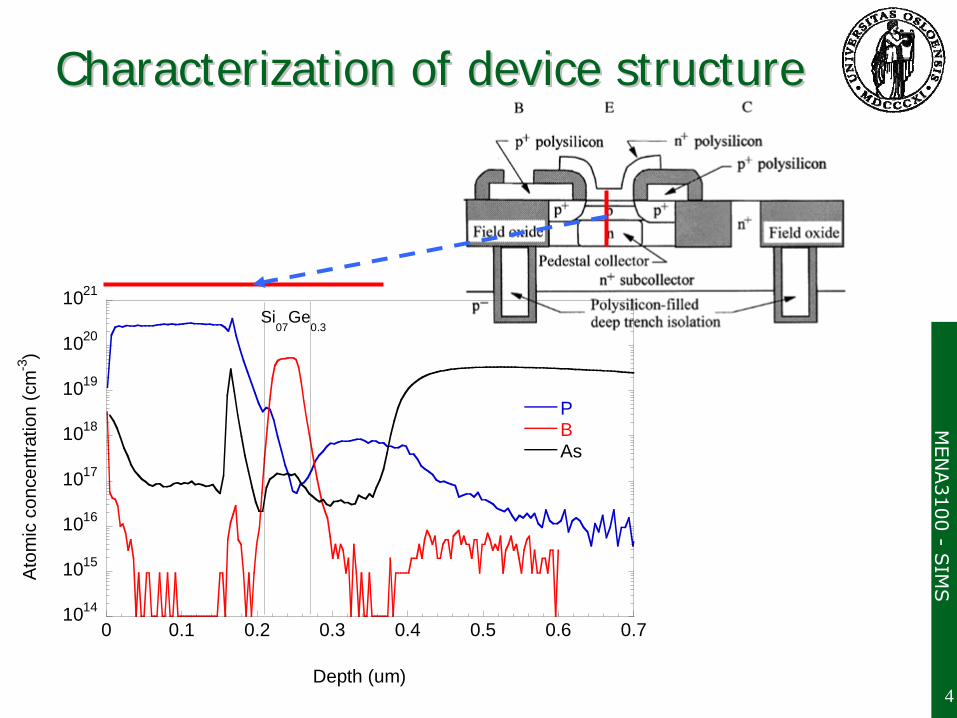
Characterization of device structureCharacterization of device structure
1014
1015
1016
1017
1018
1019
1020
1021
0 0.1 0.2 0.3 0.4 0.5 0.6 0.7
PBAs
Atom
ic c
once
ntra
tion
(cm
-3)
Depth (um)
Si07
Ge0.3
MEN
A3100 -
SIM
S
5
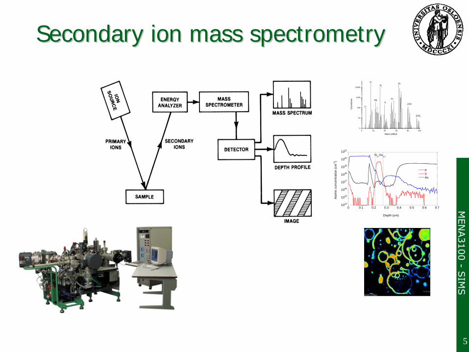
Secondary ion mass spectrometrySecondary ion mass spectrometry
0 20 40 60 80 1001
10
100
1000
10000
Cou
nts/
sec
Mass (AMU)
Li
OO
2
K
Zn
ZnO
ZnO2
Na Cr
1014
1015
1016
1017
1018
1019
1020
1021
0 0.1 0.2 0.3 0.4 0.5 0.6 0.7
PBAs
Atom
ic c
once
ntra
tion
(cm
-3)
Depth (um)
Si07
Ge0.3

MEN
A3100 -
SIM
S
6
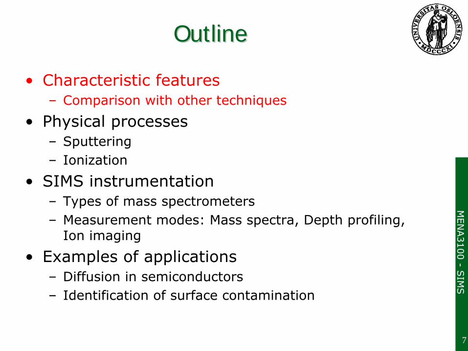
OutlineOutline
•
Characteristic features–
Comparison with other techniques
•
Physical processes–
Sputtering
–
Ionization
•
SIMS instrumentation–
Types of mass spectrometers
–
Measurement modes: Mass spectra, Depth profiling, Ion imaging
•
Examples of applications–
Diffusion in semiconductors
–
Identification of surface contamination
MEN
A3100 -
SIM
S
7
OutlineOutline
•
Characteristic features–
Comparison with other techniques
•
Physical processes–
Sputtering
–
Ionization
•
SIMS instrumentation–
Types of mass spectrometers
–
Measurement modes: Mass spectra, Depth profiling, Ion imaging
•
Examples of applications–
Diffusion in semiconductors
–
Identification of surface contamination
MEN
A3100 -
SIM
S
8
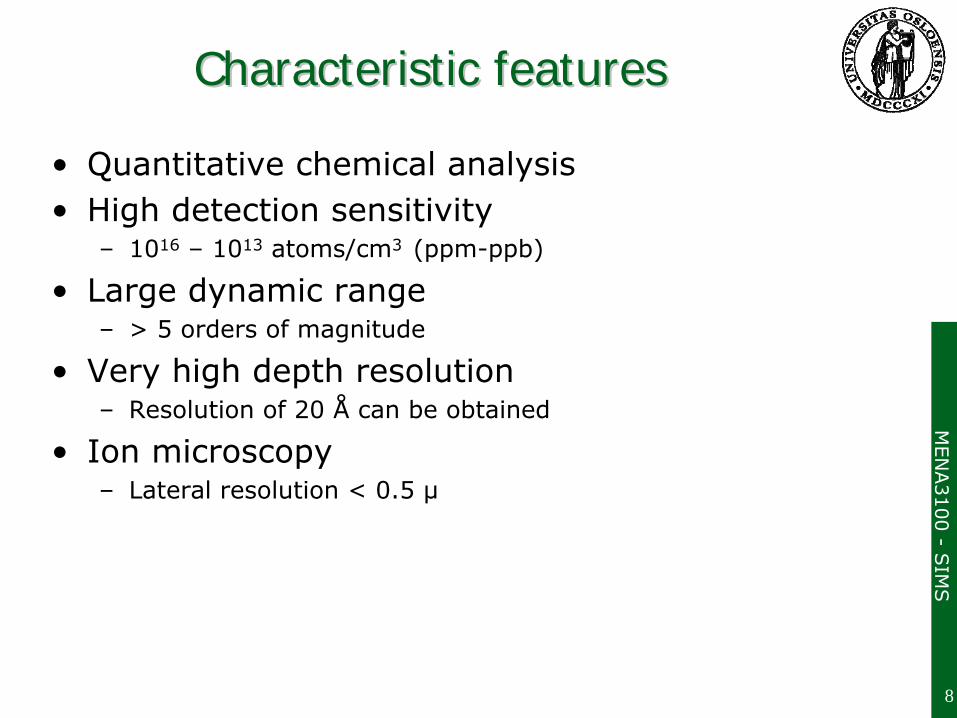
Characteristic featuresCharacteristic features
•
Quantitative chemical analysis•
High detection sensitivity–
1016
– 1013
atoms/cm3 (ppm-ppb)
•
Large dynamic range–
> 5 orders of magnitude
•
Very high depth resolution–
Resolution of 20 Å
can be obtained
•
Ion microscopy–
Lateral resolution < 0.5 µ
MEN
A3100 -
SIM
S
9
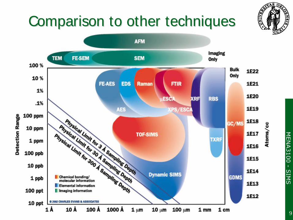
Comparison to other techniquesComparison to other techniques
MEN
A3100 -
SIM
S
10
OutlineOutline
•
Characteristic features–
Comparison with other techniques
•
Physical processes–
Sputtering
–
Ionization
•
SIMS instrumentation–
Types of mass spectrometers
–
Measurement modes: Mass spectra, Depth profiling, Ion imaging
•
Examples of applications–
Diffusion in semiconductors
–
Identification of surface contamination
MEN
A3100 -
SIM
S
11
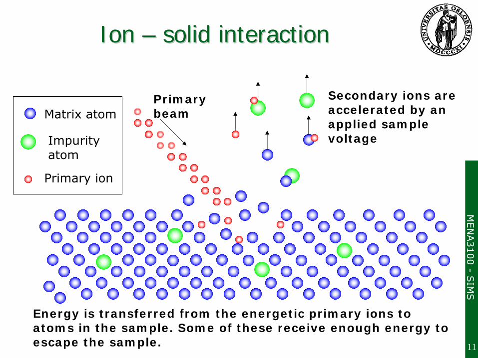
Ion Ion –– solid interactionsolid interaction
Matrix atom
Impurityatom
Primary ion
Secondary ions are accelerated by an applied sample voltage
Primary beam
Energy is transferred from the energetic primary ions to atoms in the sample. Some of these receive enough energy to escape the sample.

MEN
A3100 -
SIM
S
12
SputteringSputtering
Sigmund P. Theory of Sputtering, Phys. Rev. 184(2), 383 (1969)
Sputtering Yield:number of sputtered atoms per incoming ion
( ) ⎟⎟⎠
⎞⎜⎜⎝
⎛=
it
in
0
iti E
ESUKES
( ) ( ) ( ){ }8/3n 383/1ln5.0 ξξξξ ++=S
Sputtering yield:
( ) ( ) [ ]( ) 50.05for 3
keV5.321
it6/5
tiit
2/13/2t
3/2ititiit
≤≤≈
++=
ZZZZK
ZZZZMME
Mi , Zi : Ion mass and atomic numberMt , Zt : Target mass and atomic numberU0 : Surface escape barrier in eVEi : Ion energy
Nuclear stopping cross-section:Sputtering is a multiple collision process involving a cascade of moving target atoms, this cascade may extend over a considerable region inside the target.

MEN
A3100 -
SIM
S
13
SputteringSputtering
•
Dependence of ion
MEN
A3100 -
SIM
S
14
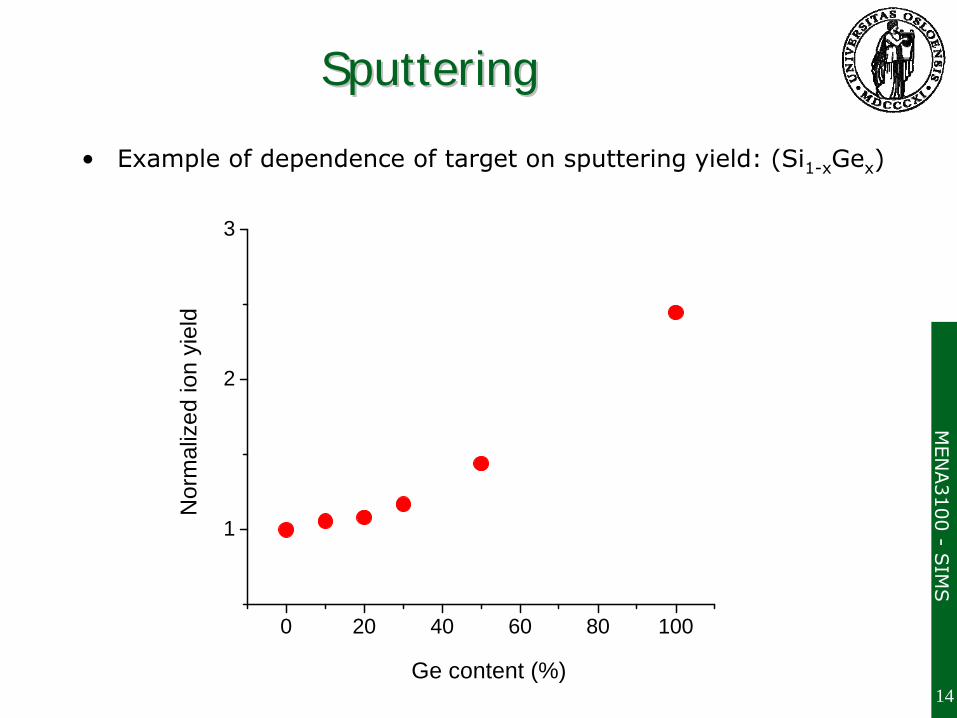
SputteringSputtering
•
Example of dependence of target on sputtering yield: (Si1-x
Gex
)
0 20 40 60 80 100
1
2
3
Nor
mal
ized
ion
yiel
d
Ge content (%)

MEN
A3100 -
SIM
S
15
SputteringSputtering
•
Example of sputtering yield:
200 µm
0 100 200 300 400 500
-1,0
-0,8
-0,6
-0,4
-0,2
0,0
Dep
th (µ
m)
Width (µm)
Material removed: 1×200×200 µ3
= 4×10⁻⁸
cm3
≈
2×10¹⁵
atoms
Current: 200 nASputtering time: 700 sec
Incoming ions: 200×10-9A ×
6.24×1018
ions/C ×
700 sec = 9x10¹⁴
ions
Sputtering Yield = 2.2 atoms/ion

MEN
A3100 -
SIM
S
16
SputteringSputtering
•
Example of sputtering of polycrystalline Fe surface
The erosion rate is different for the different grains: Sputtering yield vary with the crystal orientation
MEN
A3100 -
SIM
S
17
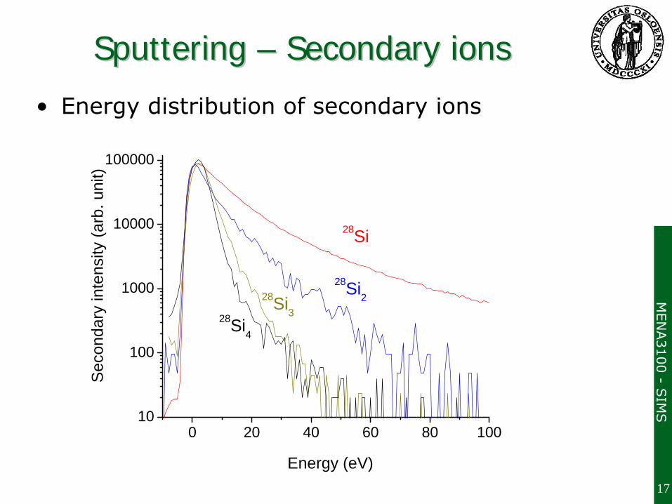
Sputtering Sputtering –– Secondary ionsSecondary ions
•
Energy distribution of secondary ions
0 20 40 60 80 10010
100
1000
10000
100000
28Si4
28Si3
28Si2
Sec
onda
ry in
tens
ity (a
rb. u
nit)
Energy (eV)
28Si
MEN
A3100 -
SIM
S
18
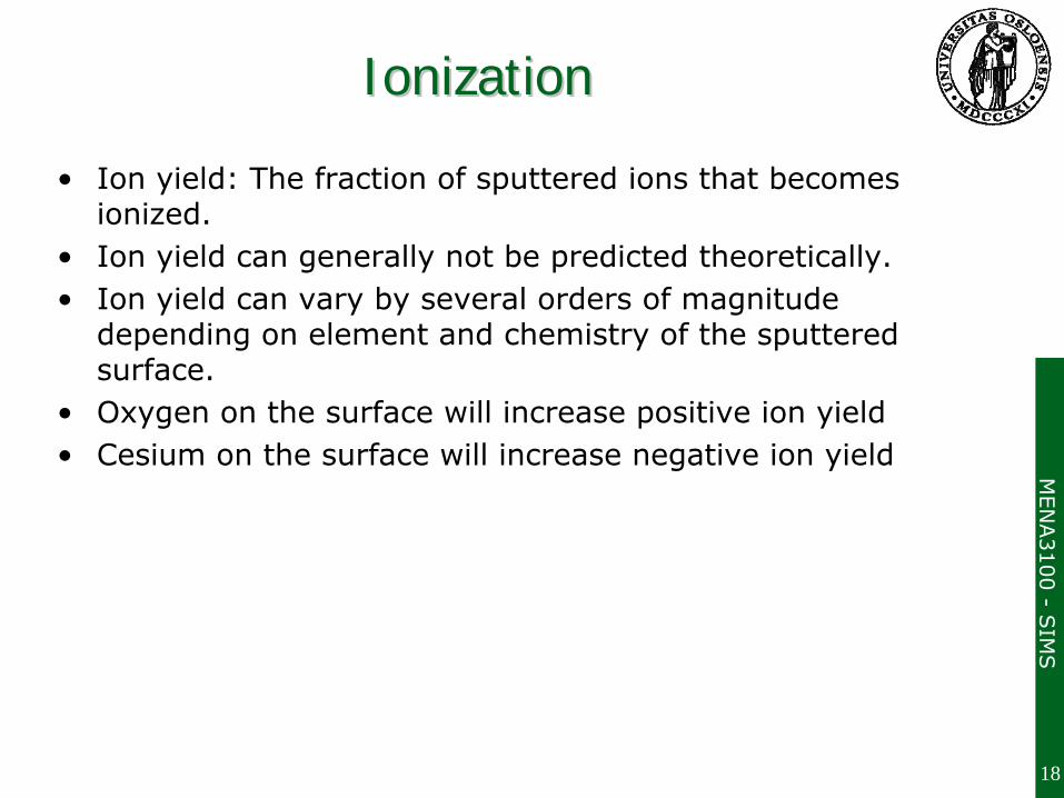
IonizationIonization
•
Ion yield: The fraction of sputtered ions that becomes ionized.
•
Ion yield can generally not be predicted theoretically.•
Ion yield can vary by several orders of magnitude depending on element and chemistry of the sputtered surface.
•
Oxygen on the surface will increase positive ion yield•
Cesium on the surface will increase negative ion yield
MEN
A3100 -
SIM
S
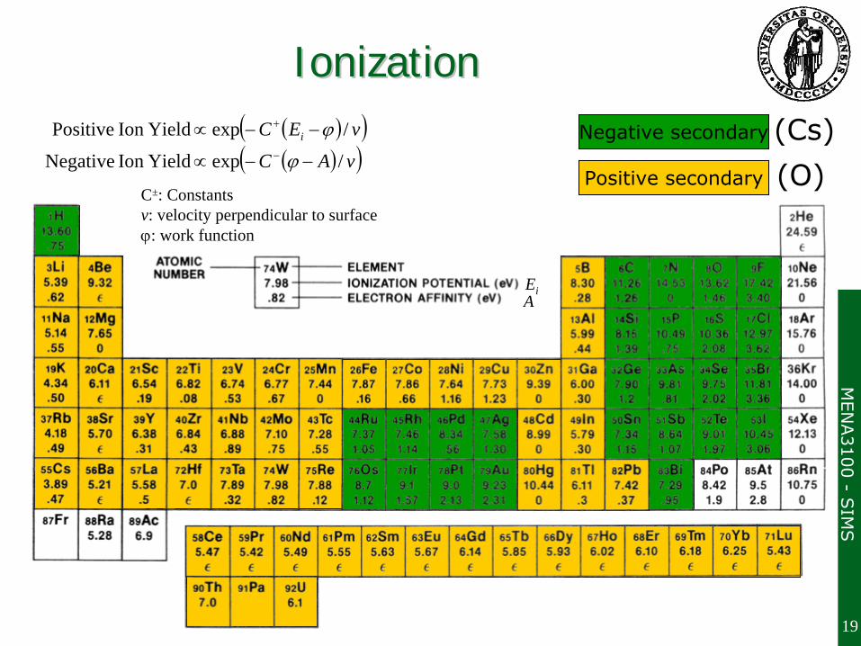
19
IonizationIonizationNegative secondary
Positive secondary
( )( )( )( )vAC
vEC i
/exp YieldIon Negative
/exp YieldIon Positive
−−∝
−−∝−
+
ϕ
ϕ
EiA
C±: Constantsv: velocity perpendicular to surfaceϕ: work function
(Cs)
(O)

MEN
A3100 -
SIM
S
20
IonizationIonization
64 66 68 70100
101
102
103
104
105
106
107
Sec
onda
ry In
tens
ity(c
ps)
M/q (AMU)
Negative modePositive mode
Mass
spectrum
of ZnO, Zn peaks.64Zn
(48.6%)66Zn
(27.9%)
67Zn
(4.1%)
68Zn
(18.8%)
70Zn
(0.6%)
MEN
A3100 -
SIM
S
21
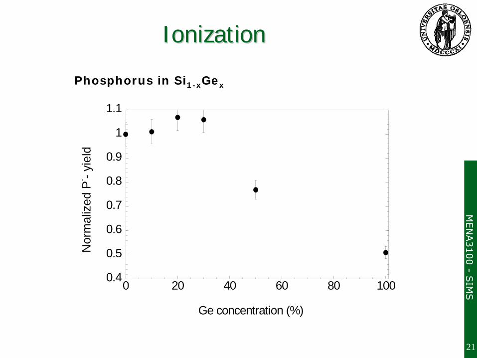
IonizationIonization
0.4
0.5
0.6
0.7
0.8
0.9
1
1.1
0 20 40 60 80 100
Nor
mal
ized
P- - y
ield
Ge concentration (%)
Phosphorus in Si1-x Gex
MEN
A3100 -
SIM
S
22
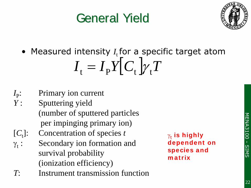
General YieldGeneral Yield
•
Measured intensity It for a specific target atom
[ ] TCYII ttPt γ=
IP : Primary ion current Y : Sputtering yield
(number of sputtered particles per impinging primary ion)
[Ct ]: Concentration of species t γt : Secondary ion formation and
survival probability (ionization efficiency)
T: Instrument transmission function
γt
is highly dependent on species and matrix

MEN
A3100 -
SIM
S
23
OutlineOutline
•
Characteristic features–
Comparison with other techniques
•
Physical processes–
Sputtering
–
Ionization
•
SIMS instrumentation–
Types of mass spectrometers
–
Measurement modes: Mass spectra, Depth profiling, Ion imaging
•
Examples of applications–
Diffusion in semiconductors
–
Identification of surface contamination

MEN
A3100 -
SIM
S
24
The SIMS instrumentThe SIMS instrument
MEN
A3100 -
SIM
S
25
The SIMS instrumentThe SIMS instrument
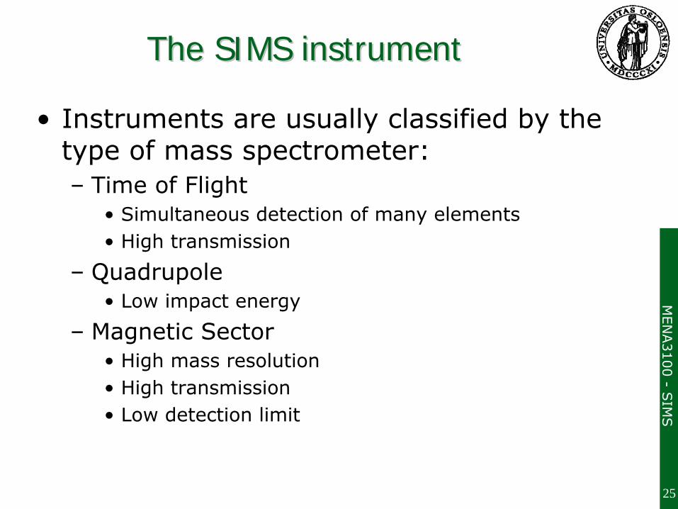
•
Instruments are usually classified by the type of mass spectrometer:–
Time of Flight•
Simultaneous detection of many elements
•
High transmission
–
Quadrupole•
Low impact energy
–
Magnetic Sector•
High mass resolution
•
High transmission•
Low detection limit

MEN
A3100 -
SIM
S
26
Time of Time of FlightFlight SIMSSIMS
MEN
A3100 -
SIM
S
27
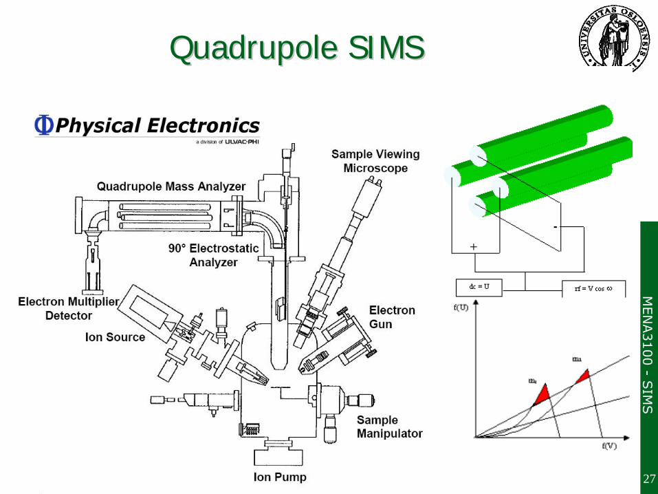
QuadrupoleQuadrupole SIMSSIMS

MEN
A3100 -
SIM
S
28
Magnetic sector Magnetic sector -- mass mass spectrometer spectrometer
sample
detector
ion source
electrostatic sector analyser
magnetic sector analyser
Primary beam
Seco
ndar
y be
amre rm
E0B
Lorenz’ force: ( )BvEF ×+= qq
Centripetal force:rr
mv rF2
−=
2
e0 r
mvqE =
Electrostaticsector analyser
2
mrmvqvB =
Magneticsector analyser
( ) 2
0e
m
ErBr
qm
=

MEN
A3100 -
SIM
S
29
Secondary ion mass spectrometrySecondary ion mass spectrometry
( )2m
0 e
Brmq E r
=
sample
detector
ion source
electrostatic sector analyser
magnetic sector analyser
Primary beam
Seco
ndar
y be
am
re rm
E0B
0 100 200 300 400 500 6001
10
100
1000
10000
Inte
nsity
(cou
nts/
sec)
Sputter time (sec)
Depth profile
0 20 40 60 80 1001
10
100
1000
10000
Cou
nts/
sec
Mass (AMU)
Mass spectrum
Ion image
20 µm
MEN
A3100 -
SIM
S
30
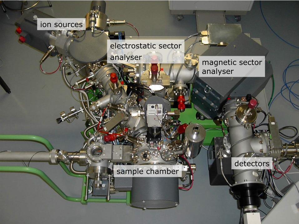
InstrumentationInstrumentationion sources
sample chamber
electrostatic
sector
analysermagnetic
sector
analyser
detectors
MEN
A3100 -
SIM
S
31
MassMass InterferenceInterference
11,5 12,0 12,5 13,0 13,5
100
101
102
103
104
105
106
Sec
onda
ry in
tens
ity (c
ps)
Mass (AMU)
Mass
spectrum of graphite
91.6%
8.4%

MEN
A3100 -
SIM
S
32
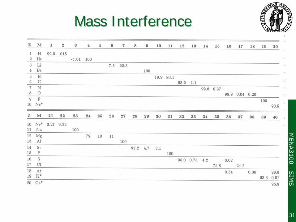
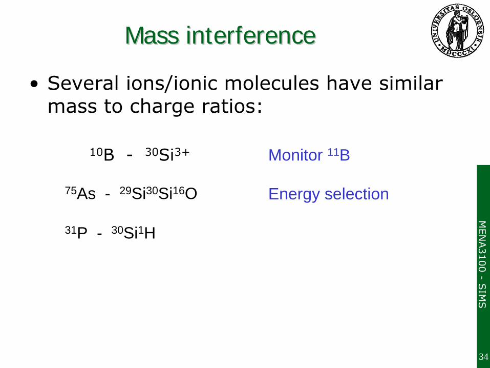
Mass interferenceMass interference
•
Several ions/ionic molecules have similar mass to charge ratios:
10B -
30Si3+ Monitor 11B
75As - 29Si30Si16O
MEN
A3100 -
SIM
S
33
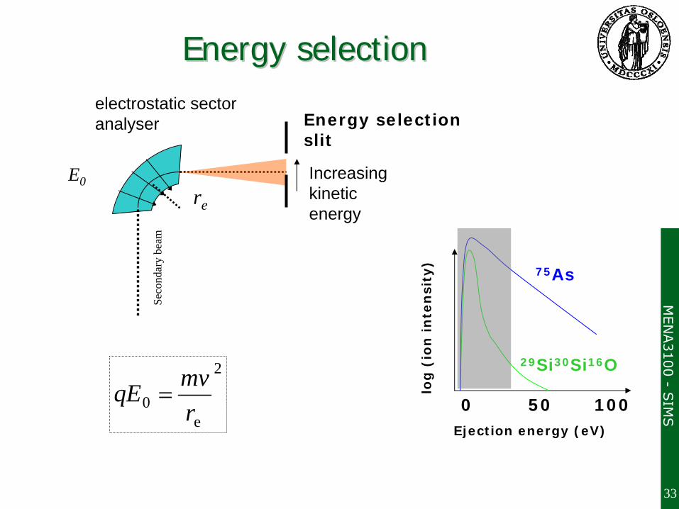
Energy selectionEnergy selectionelectrostatic sector analyser
Seco
ndar
y be
am
re
E0
2
e0 r
mvqE =
Increasing kinetic energy
Energy selection slit
Ejection energy (eV)lo
g (
ion
in
ten
sity
)
75As
29Si30Si16O
0 50 100
MEN
A3100 -
SIM
S
34
MassMass interferenceinterference
•
Several
ions/ionic
molecules
have similar mass
to charge
ratios:
10B -
30Si3+ Monitor 11B
75As - 29Si30Si16O Energy selection
31P - 30Si1H

MEN
A3100 -
SIM
S
35
HighHigh massmass resolutionresolution
30,85 30,90 30,95 31,00 31,05 31,10
100
1000
10000
Inte
nsity
(cou
nts/
sec)
Mass (AMU)
magnetic sector analyser
rm
B
2
mrmvqvB =
Exit slit
Discriminating
between
31P and 30Si1H:
M(31P) = 30.973761M(30Si1H) =30.98160
30,85 30,90 30,95 31,00 31,05 31,10
100
1000
10000
Inte
nsity
(cou
nts/
sec)
Mass (AMU)
31P
30Si1H
ΔΜ/Μ = 4000

MEN
A3100 -
SIM
S
36
Mass interferenceMass interference
•
Several ions/ionic molecules have similar mass to charge ratios:
10B -
30Si3+ Monitor 11B
75As - 29Si30Si16O Energy selection
31P - 30Si1H High mass resolution
MEN
A3100 -
SIM
S
37
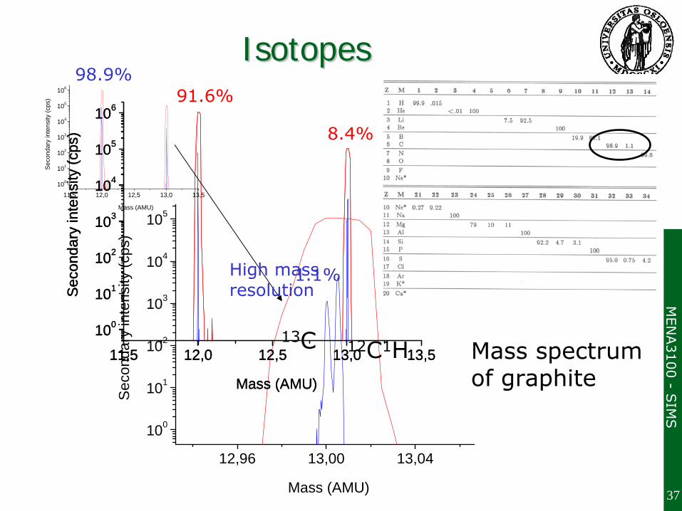
IsotopesIsotopes
12,96 13,00 13,04
100
101
102
103
104
105
Sec
onda
ry in
tens
ity (c
ps)
Mass (AMU)
11,5 12,0 12,5 13,0 13,5
100
101
102
103
104
105
106
Sec
onda
ry in
tens
ity (c
ps)
Mass (AMU)
11,5 12,0 12,5 13,0 13,5
100
101
102
103
104
105
106
Sec
onda
ry in
tens
ity (c
ps)
Mass (AMU)
Mass
spectrum of graphite
11,5 12,0 12,5 13,0 13,5
100
101
102
103
104
105
106
Sec
onda
ry in
tens
ity (c
ps)
Mass (AMU)
91.6%
8.4%
98.9%
1.1%
13C 12C1H
High
mass
resolution

MEN
A3100 -
SIM
S
38
MassMass spectrumspectrum
0 20 40 60 80 1001
10
100
1000
10000
Cou
nts/
sec
Mass (AMU)
Li
OO2
K
Zn
ZnO
ZnO2
Na Cr
Mass
spectrum
of a ZnO-sample
with
traces of Li, Na, K, and Cr.
MEN
A3100 -
SIM
S
39
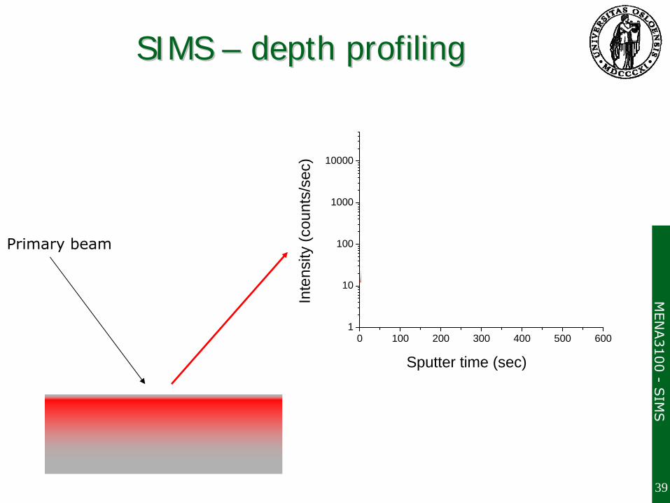
SIMS SIMS –– depth profilingdepth profiling
0 100 200 300 400 500 6001
10
100
1000
10000
Inte
nsity
(cou
nts/
sec)
Sputter time (sec)
Primary beam

MEN
A3100 -
SIM
S
40
0 100 200 300 400 500 600 700
1
10
100
Inte
nsity
(cou
nts/
sec)
Sputter time (sec)
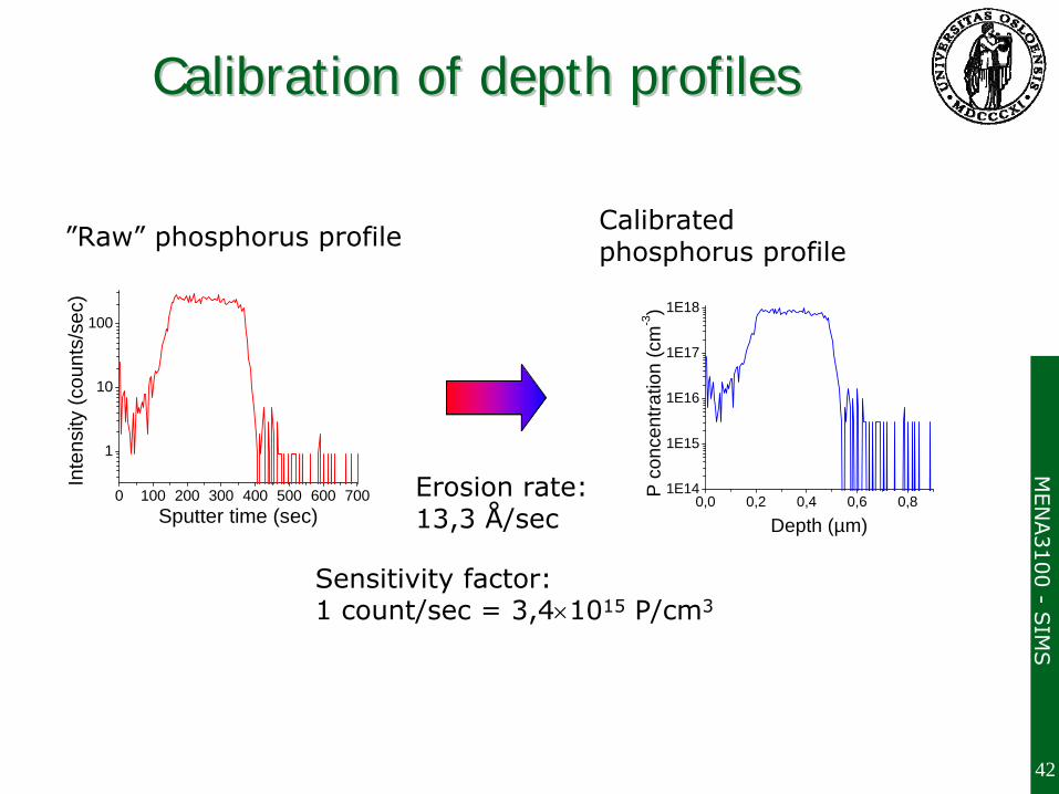
CalibrationCalibration of of depthdepth profilesprofiles
”Raw”
phosphorus
profile
0 100 200 300 400 500
-1,0
-0,8
-0,6
-0,4
-0,2
0,0
Dep
th (µ
m)
Width (µm)
Depth calibration
Sputter time: 700 sec Depth: 9310 Å
Erosion rate:13,3 Å/sec

MEN
A3100 -
SIM
S
41
0 100 200 300 400 500 600 700
1
10
100
Inte
nsity
(cou
nts/
sec)
Sputter time (sec)
CalibrationCalibration of of depthdepth profilesprofiles
[ ] TCYII ttPt γ=
”Raw”
phosphorus
profile
( )[ ]t1 CS=
S: Sensitivity
factor
0 100 200 300 400 500 6000,1
1
10
100
1000
10000
Inte
nsity
(cou
nts/
sec)
Sputter time (sec)
Concentration calibration
Ion implanted sample:P dose 1e15 P/cm2
sensitivity factor:Relate the intensity to atomic concentration
( )∫=
xxIS
d Dose
Sensitivity factor:1 count/sec = 3,4×10¹⁵
P/cm3
MEN
A3100 -
SIM
S
42
Calibration of depth profilesCalibration of depth profiles
0,0 0,2 0,4 0,6 0,81E14
1E15
1E16
1E17
1E18
P co
ncen
tratio
n (c
m-3)
Depth (µm)0 100 200 300 400 500 600 700
1
10
100
Inte
nsity
(cou
nts/
sec)
Sputter time (sec)
”Raw”
phosphorus profile
Calibratedphosphorus profile
Erosion rate:13,3 Å/sec
Sensitivity factor:1 count/sec = 3,4×10¹⁵
P/cm3
MEN
A3100 -
SIM
S
43
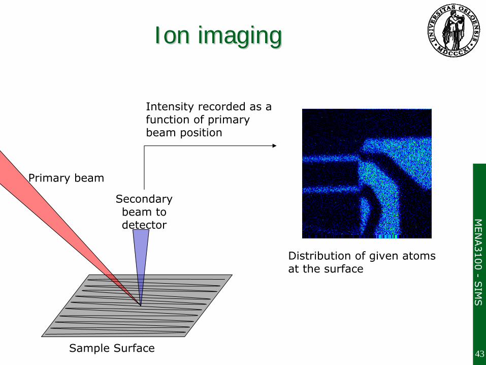
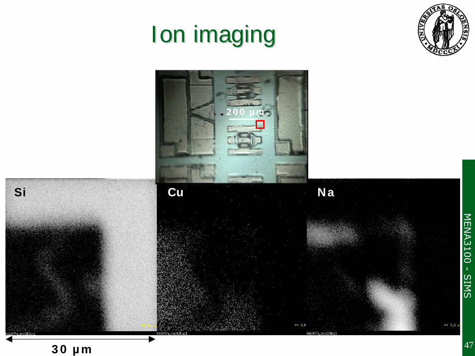
Ion imagingIon imaging
Distribution of given atoms at the surface
Primary
beam
Secondary beam to detector
Intensity recorded as a function of primary beam position
Sample Surface
MEN
A3100 -
SIM
S
44
Examples of ApplicationsExamples of Applications
•
Depth profiling–
Dopant
diffusion in semiconductors
–
Isotope enriched superstructures
•
Ion imaging–
Characterizing contacts on sample surface
–
Impurity after processing
•
Mass spectrum–
N doping of MOCVD grown ZnO
MEN
A3100 -
SIM
S
45
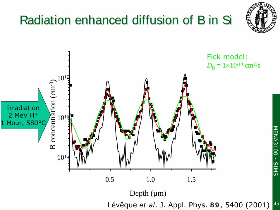
Radiation enhanced diffusion of B in SiRadiation enhanced diffusion of B in Si
Irradiation
2 MeV
H+
1 Hour, 580°C
Depth (µm)
B c
once
ntra
tion
(cm
-3)
0.5 1.0 1.5
1015
1016
1017
Fick
model:
DB = 1×10-14 cm2/s
Lévêque
et al. J. Appl. Phys. 89, 5400 (2001)
MEN
A3100 -
SIM
S
46
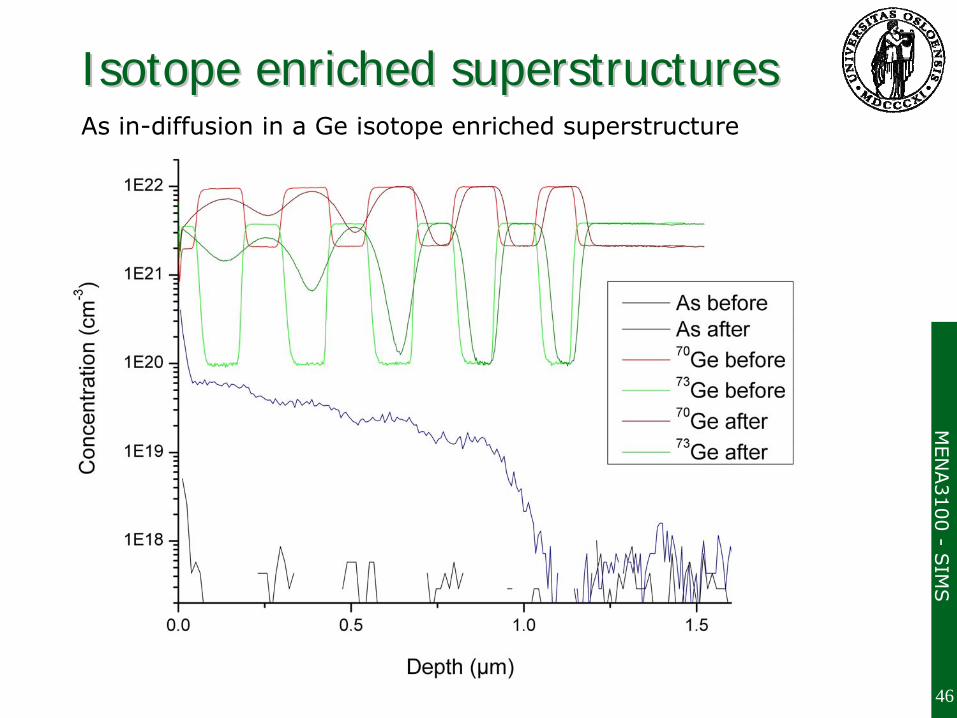
Isotope enriched superstructuresIsotope enriched superstructuresAs in-diffusion in a Ge
isotope enriched superstructure
MEN
A3100 -
SIM
S
47
Ion imagingIon imaging
30 µm
200 µm
Si Cu Na
MEN
A3100 -
SIM
S
48
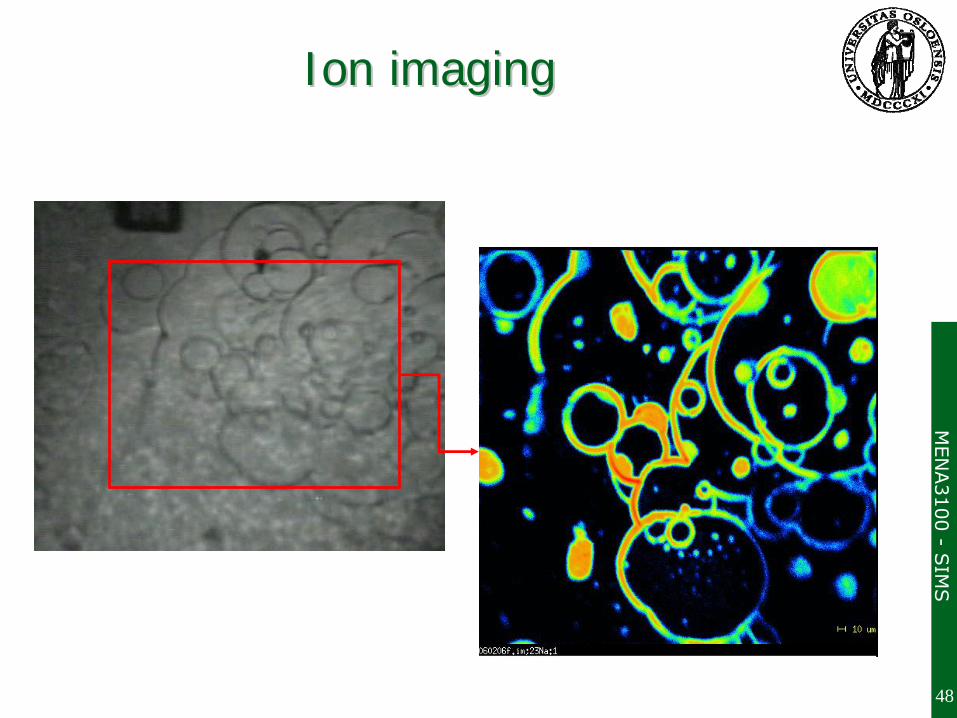
Ion Ion imagingimaging
MEN
A3100 -
SIM
S
49
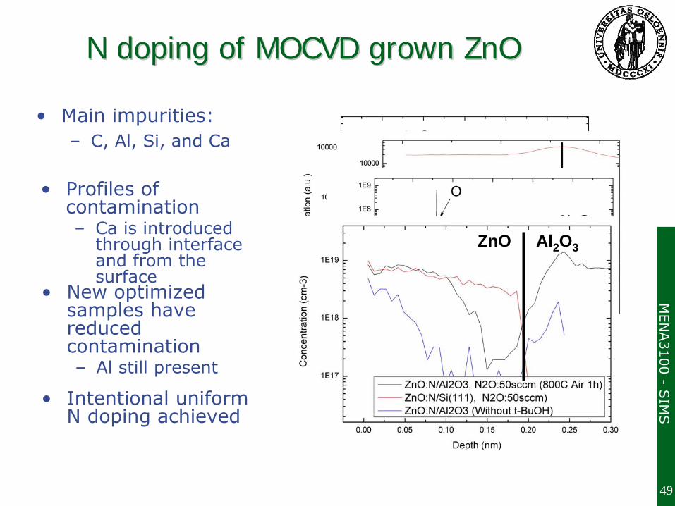
N doping of MOCVD grown N doping of MOCVD grown ZnOZnO
•
Main impurities:–
C, Al, Si, and Ca
ZnO Al2 O3
•
Profiles of contamination–
Ca is introduced through interface and from the surface
•
New optimized samples have reduced contamination–
Al still present
•
Intentional uniform N doping achieved
Related Documents


