DIGITAL SYSTEM DESIGN LAB MANUAL B.E (ECE) – FULL TIME III SEMESTER (For Private Circulation) DEPARTMENT OF ELECTRONICS & COMMUNICATION ENGINEERING SRI CHANDRASEKHARENDRA SARASWATHI VISWA MAHAVIDYALAYA (A University U/S 3 of UGC Act 1956) (Accredited with ‘B’ Grade by NAAC) Enathur, Kanchipuram – 631561 Prepared By K.M.Sivakumar.B.E,M.E. Department of ECE, SCSVMV University

Welcome message from author
This document is posted to help you gain knowledge. Please leave a comment to let me know what you think about it! Share it to your friends and learn new things together.
Transcript

DIGITAL SYSTEM DESIGN
LAB MANUAL
B.E (ECE) – FULL TIMEIII SEMESTER
(For Private Circulation)
DEPARTMENT OF ELECTRONICS & COMMUNICATION ENGINEERING
SRI CHANDRASEKHARENDRA SARASWATHI VISWAMAHAVIDYALAYA
(A University U/S 3 of UGC Act 1956)
(Accredited with ‘B’ Grade by NAAC)Enathur, Kanchipuram – 631561
Prepared ByK.M.Sivakumar.B.E,M.E.
Department of ECE, SCSVMV University


EXPERIMENTS USING DIGITAL IC TRAINER KIT
1. STUDY OF LOGIC GATES
2. DESIGN OF ADDER AND SUBTRACTOR
3. DESIGN AND IMPLEMENTATION OF CODE CONVERTER
4. DESIGN OF 4-BIT ADDER AND SUBTRACTOR
5. DESIGN AND IMPLEMENTATION OF MAGNITUDE COMPARATOR
6. DESIGN AND IMPLEMENTATION OF MULTIPLEXER AND DEMULTIPLEXER
7. DESIGN AND IMPLEMENTATION OF ENCODER AND DECODER
8. CONSTRUCTION AND VERIFICATION OF 4 BIT RIPPLE COUNTER AND MOD 10/
MOD 12 RIPPLE COUNTER
9. DESIGN AND IMPLEMENTATION OF 3 BIT SYNCHRONOUS UP/DOWN COUNTER
10. DESIGN AND IMPLEMENTATION OF SHIFT REGISTER
11. BOOLEAN OPERATIONS USING LABVIEW
EXPERIMENTS USING XILINX ISE SIMULATOR (VHDL/VERILOG)
12. DESIGN ENTRY AND SIMULATION OF COMBINATIONAL LOGIC CIRCUITS
USING XILINX ISE SIMULATOR
13. IMPLEMENTATION OF FLIP-FLOPS USING XILINX ISE SIMULATOR
14. IMPLEMENTATION OF COUNTERS USING XILINX ISE SIMULATOR
EXPERIMENTS USING NI MULTISIM SOFTWARE
15. IMPLEMENTATION OF BASIC LOGIC GATES
16. TESTING OF LOGIC GATES
17. HALF ADDER/SUBTRACTOR & FULL ADDER/SUBTRACTOR
18. DECODERS & ENCODERS: 2-4 DECODER & 3-8 DECODER
19. IMPLEMENTATION OF FLIP-FLOPS :S-R FLIP FLOP & J-K FLIP FLOP
20. DESIGN AND IMPLEMENTATION OF MULTIPLEXER AND DEMULTIPLEXER
21. FOUR BIT MAGNITUDE COMPARATOR
22. 4 BIT SYNCHRONOUS COUNTER
EXPERIMENTS USING MATLAB SIMULINK MODELING
23. DESIGN OF ADDER & SUBTRACTOR USING MATLAB SIMULINK
24. TESTING OF BASIC LOGIC GATES USING MATLAB SIMULINK
25. MASTER – SLAVE J K FLIP FLOP MODELING USING MATLAB SIMULINK
26. DESIGN OF MULTIPLEXER & DEMULTIPLXER USING MATLAB SIMULINK
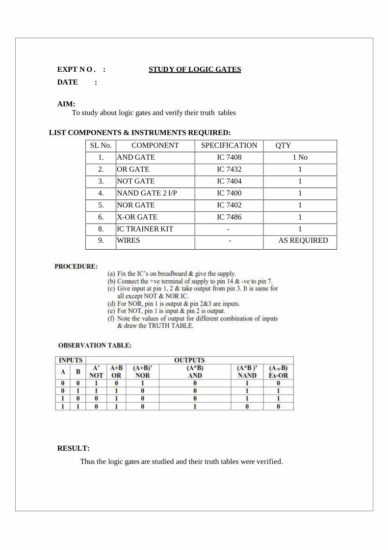
EXPT N O . : STUDY OF LOGIC GATES
DATE :
AIM:To study about logic gates and verify their truth tables
LIST COMPONENTS & INSTRUMENTS REQUIRED:
SL No. COMPONENT SPECIFICATION QTY
1. AND GATE IC 7408 1 No
2. OR GATE IC 7432 1
3. NOT GATE IC 7404 1
4. NAND GATE 2 I/P IC 7400 1
5. NOR GATE IC 7402 1
6. X-OR GATE IC 7486 1
8. IC TRAINER KIT - 1
9. WIRES - AS REQUIRED
RESULT:
Thus the logic gates are studied and their truth tables were verified.
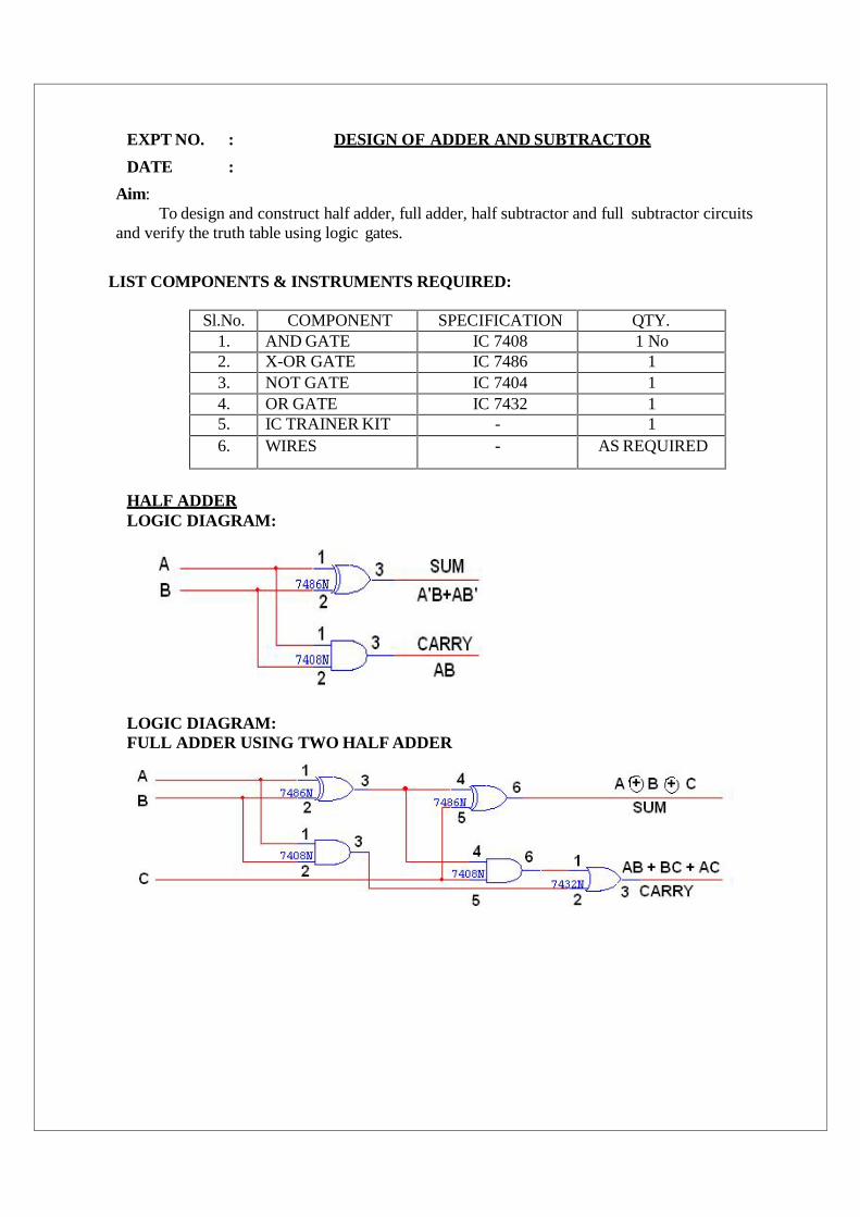
EXPT NO. : DESIGN OF ADDER AND SUBTRACTOR
DATE :
Aim:To design and construct half adder, full adder, half subtractor and full subtractor circuits
and verify the truth table using logic gates.
LIST COMPONENTS & INSTRUMENTS REQUIRED:
Sl.No. COMPONENT SPECIFICATION QTY.1. AND GATE IC 7408 1 No2. X-OR GATE IC 7486 13. NOT GATE IC 7404 14. OR GATE IC 7432 15. IC TRAINER KIT - 16. WIRES - AS REQUIRED
HALF ADDERLOGIC DIAGRAM:
LOGIC DIAGRAM:FULL ADDER USING TWO HALF ADDER

FULL ADDER TRUTH TABLE:
A B C CARRY SUM00001111
00110011
01010101
00010111
01101001
HALF SUBTRACTOR TRUTH TABLE:
A B BORROW DIFFERENCE
0011
0101
0100
0110
LOGIC DIAGRAM:
FULL SUBTRACTOR TRUTH TABLE:A B C BORROW DIFFERENCE00001111
00110011
01010101
01110001
01101001

LOGIC DIAGRAM:
FULL SUBTRACTOR USING TWO HALF SUBTRACTOR:
PROCEDURE:(i) Connections are given as per circuitdiagram.
(ii) Logical inputs are given as per circuit diagram.
(iii) Observe the output and verify the truth table.
RESULT:Thus the half adder, full adder, half subtractor and full subtractor was designed
and their truth table is verified.

EXPT NO. : DESIGN AND IMPLEMENTATION OF CODE CONVERTER
DATE :
AIM:To design and implement 4-bit(i) Binary to gray code converter ii) Gray to binary code converter(ii) BCD to excess-3 code converter iii) Excess-3 to BCD code converter
LIST OF COMPONENTS & INSTRUMENTS REQUIRED:
Sl.No. COMPONENT SPECIFICATION QTY.
1. X-OR GATE IC 7486 12. AND GATE IC 7408 1
3. OR GATE IC 7432 1
4. NOT GATE IC 7404 1
5. IC TRAINER KIT - 16. WIRES - AS REQUIRED
LOGIC DIAGRAM:

BINARY TO GRAY CODE CONVERTORTRUTH TABLE:
| Binary input | Gray code output |
LOGIC DIAGRAM:
B3 B2 B1 B0 G3 G2 G1 G0
0000000011111111
0000111100001111
0011001100110011
0101010101010101
0000000011111111
0000111111110000
0011110000111100
0110011001100110
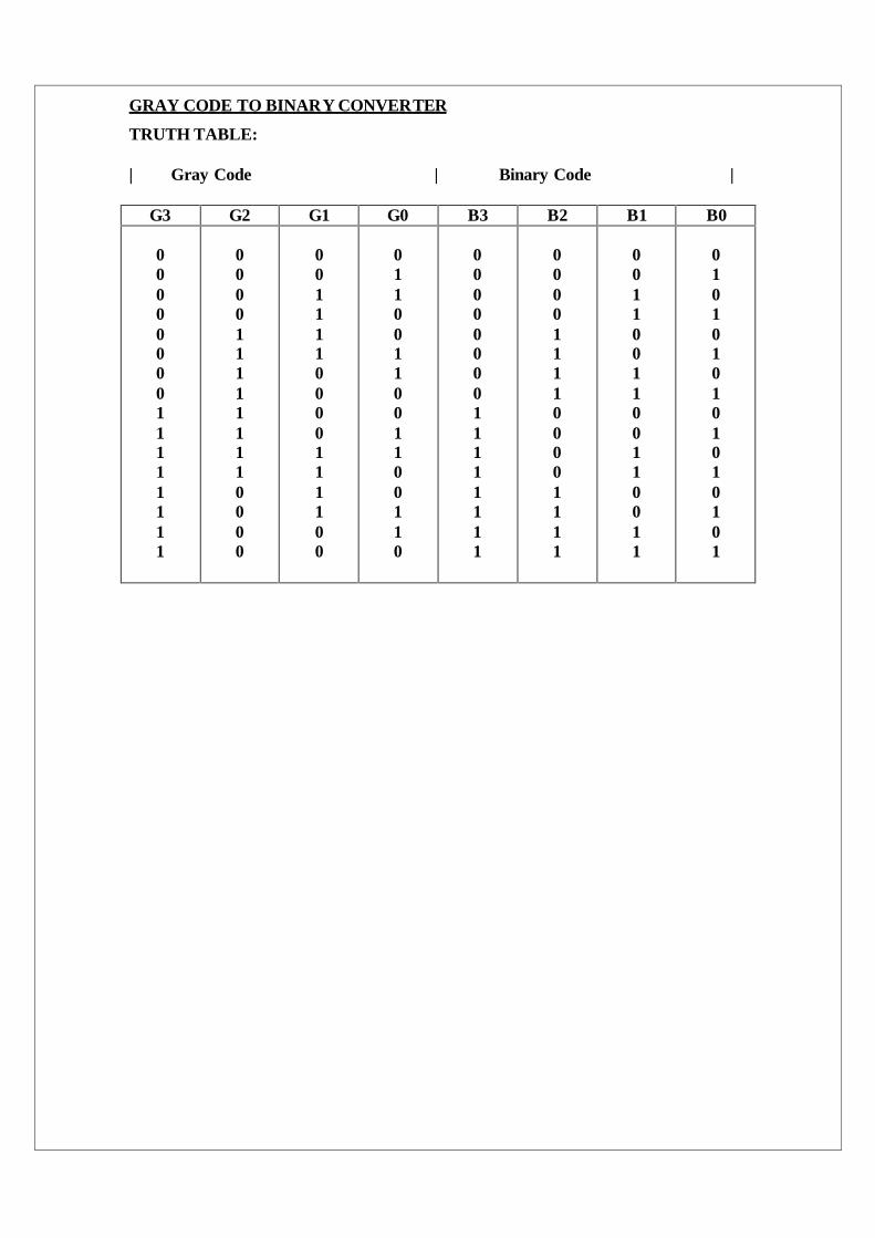
GRAY CODE TO BINARY CONVERTER
TRUTH TABLE:
| Gray Code | Binary Code |
G3 G2 G1 G0 B3 B2 B1 B0
0000000011111111
0000111111110000
0011110000111100
0110011001100110
0000000011111111
0000111100001111
0011001100110011
0101010101010101
LOGIC DIAGRAM
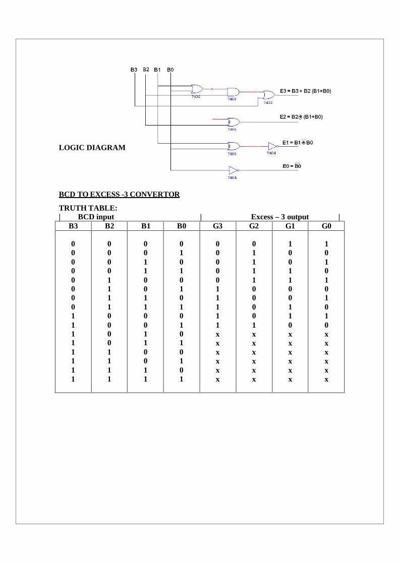
BCD TO EXCESS -3 CONVERTOR
TRUTH TABLE:| BCD input | Excess – 3 output |
B3 B2 B1 B0 G3 G2 G1 G0
0000000011111111
0000111100001111
0011001100110011
0101010101010101
0000011111xxxxxx
0111100001xxxxxx
1001100110xxxxxx
1010101010xxxxxx
34
LOGIC DIAGRAM:
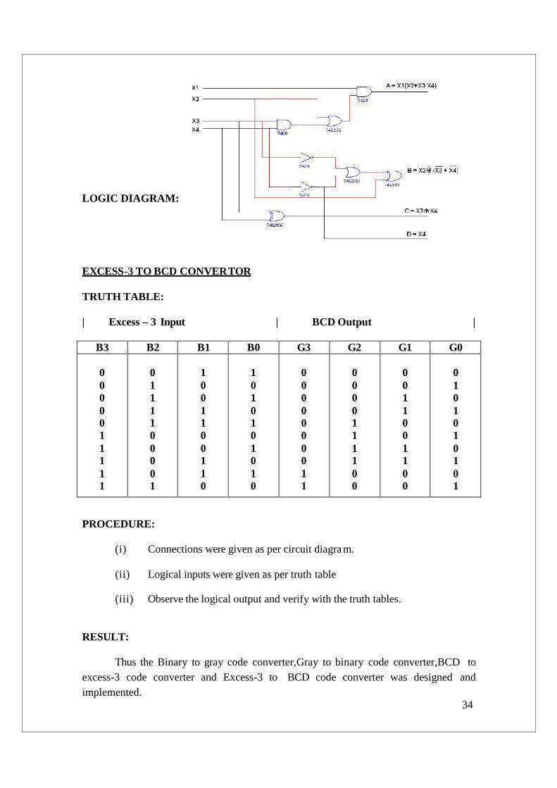
EXCESS-3 TO BCD CONVERTOR
TRUTH TABLE:
| Excess – 3 Input | BCD Output |
B3 B2 B1 B0 G3 G2 G1 G0
0000011111
0111100001
1001100110
1010101010
0000000011
0000111100
0011001100
0101010101
PROCEDURE:
(i) Connections were given as per circuit diagra m.
(ii) Logical inputs were given as per truth table
(iii) Observe the logical output and verify with the truth tables.
RESULT:
Thus the Binary to gray code converter,Gray to binary code converter,BCD toexcess-3 code converter and Excess-3 to BCD code converter was designed andimplemented.
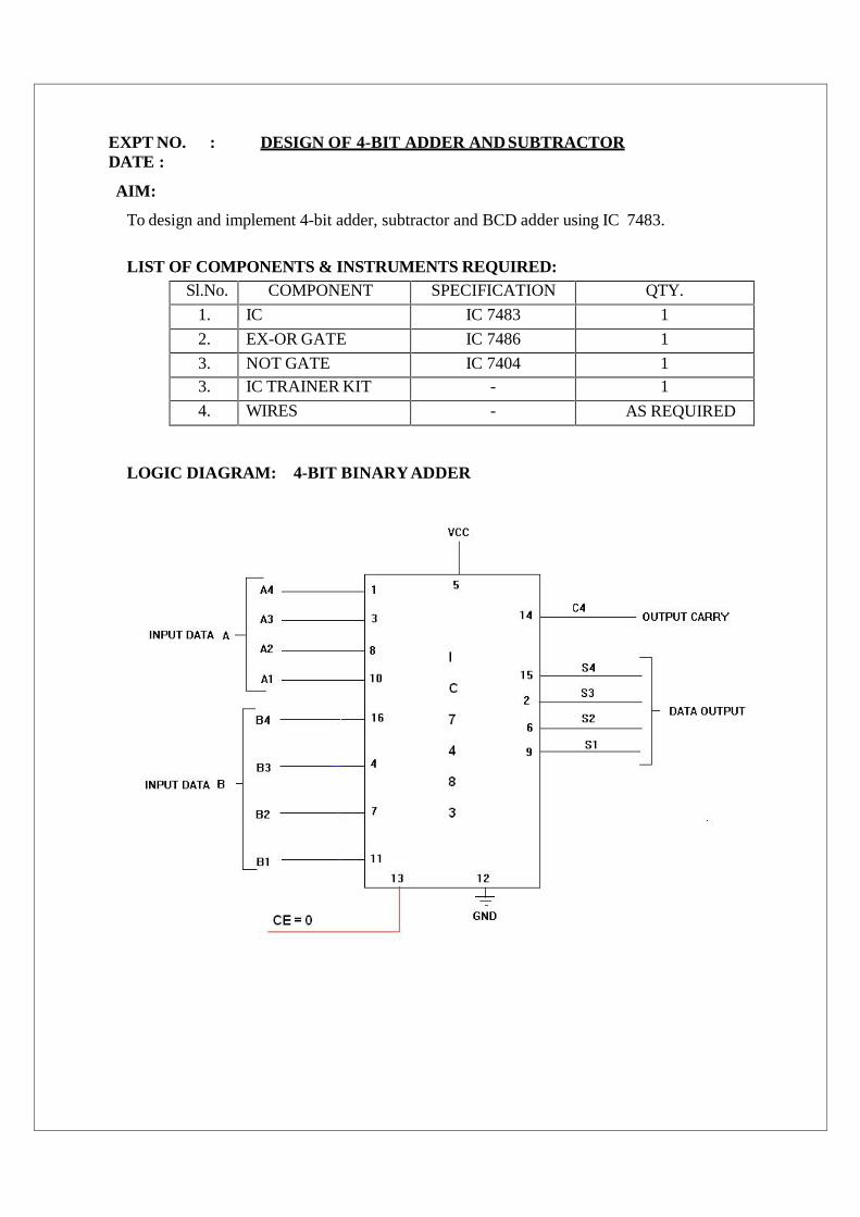
EXPT NO. : DESIGN OF 4-BIT ADDER AND SUBTRACTORDATE :
AIM:
To design and implement 4-bit adder, subtractor and BCD adder using IC 7483.
LIST OF COMPONENTS & INSTRUMENTS REQUIRED:Sl.No. COMPONENT SPECIFICATION QTY.
1. IC IC 7483 1
2. EX-OR GATE IC 7486 1
3. NOT GATE IC 7404 13. IC TRAINER KIT - 1
4. WIRES - AS REQUIRED
LOGIC DIAGRAM: 4-BIT BINARYADDER
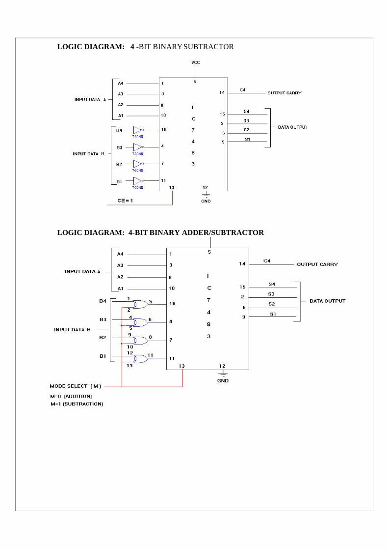
LOGIC DIAGRAM: 4 -BIT BINARYSUBTRACTOR
LOGIC DIAGRAM: 4-BIT BINARY ADDER/SUBTRACTOR

TRUTH TABLE:
Input Data A Input Data B Addition Subtraction
A4 A3 A2 A1 B4 B3 B2 B1 C S4 S3 S2 S1 B D4 D3 D2 D1
1 0 0 0 0 0 1 0 0 1 0 1 0 1 0 1 1 0
1 0 0 0 1 0 0 0 1 0 0 0 0 1 0 0 0 0
0 0 1 0 1 0 0 0 0 1 0 1 0 0 1 0 1 0
0 0 0 1 0 1 1 1 0 1 0 0 0 0 1 0 1 0
1 0 1 0 1 0 1 1 1 0 0 1 0 0 1 1 1 1
1 1 1 0 1 1 1 1 1 1 0 1 0 0 1 1 1 1
LOGIC DIAGRAM: BCD ADDER

TRUTH TABLE:
BCD SUM CARRYS4 S3 S2 S1 C0 0 0 0 00 0 0 1 00 0 1 0 00 0 1 1 00 1 0 0 00 1 0 1 00 1 1 0 00 1 1 1 01 0 0 0 01 0 0 1 01 0 1 0 11 0 1 1 11 1 0 0 11 1 0 1 11 1 1 0 11 1 1 1 1
PROCEDURE:
(i) Connections were given as per circuit diagram.(ii) Logical inputs were given as per truth table(iii) Observe the logical output and verify with the truth tables.
RESULT:
Thus the 4-bit adder, subtractor and BCD adder using IC 7483 was designed andimplemented.
EXPT NO. :
DATE :
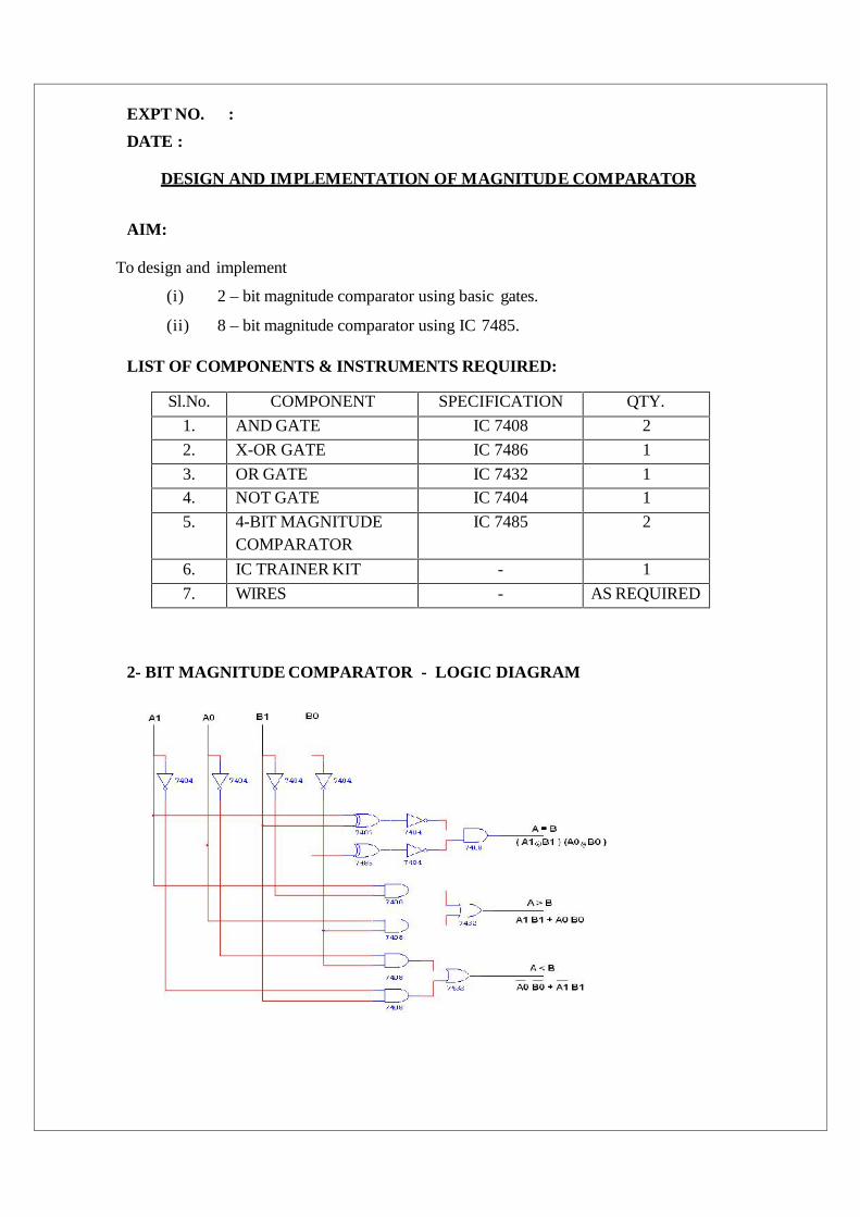
DESIGN AND IMPLEMENTATION OF MAGNITUDE COMPARATOR
AIM:
To design and implement
(i) 2 – bit magnitude comparator using basic gates.
(ii) 8 – bit magnitude comparator using IC 7485.
LIST OF COMPONENTS & INSTRUMENTS REQUIRED:
Sl.No. COMPONENT SPECIFICATION QTY.
1. AND GATE IC 7408 2
2. X-OR GATE IC 7486 1
3. OR GATE IC 7432 14. NOT GATE IC 7404 1
5. 4-BIT MAGNITUDECOMPARATOR
IC 7485 2
6. IC TRAINER KIT - 1
7. WIRES - AS REQUIRED
2- BIT MAGNITUDE COMPARATOR - LOGIC DIAGRAM
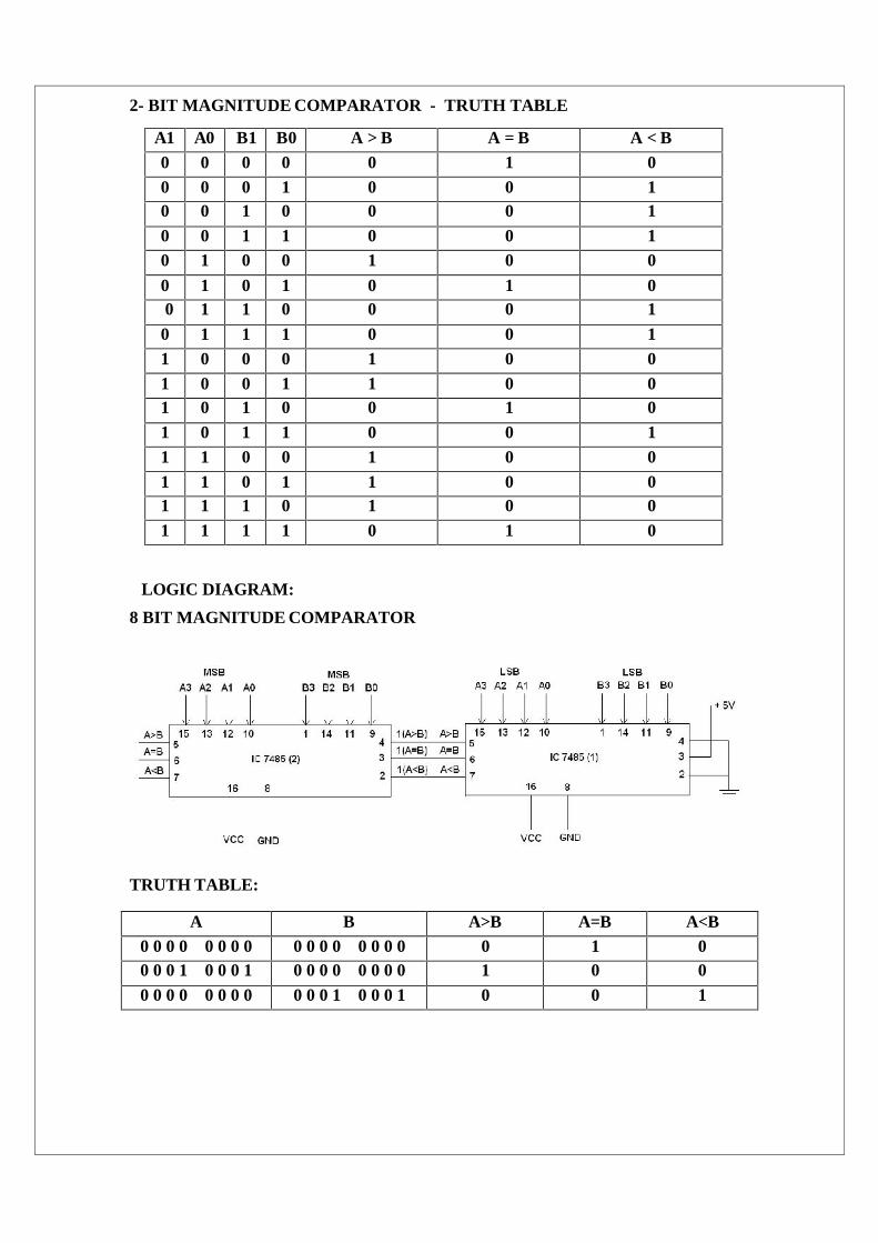
2- BIT MAGNITUDE COMPARATOR - TRUTH TABLE
A1 A0 B1 B0 A > B A = B A < B0 0 0 0 0 1 00 0 0 1 0 0 10 0 1 0 0 0 10 0 1 1 0 0 10 1 0 0 1 0 0
0 1 0 1 0 1 00 1 1 0 0 0 1
0 1 1 1 0 0 11 0 0 0 1 0 01 0 0 1 1 0 01 0 1 0 0 1 01 0 1 1 0 0 11 1 0 0 1 0 01 1 0 1 1 0 01 1 1 0 1 0 01 1 1 1 0 1 0
LOGIC DIAGRAM:
8 BIT MAGNITUDE COMPARATOR
TRUTH TABLE:
A B A>B A=B A<B0 0 0 0 0 0 0 0 0 0 0 0 0 0 0 0 0 1 00 0 0 1 0 0 0 1 0 0 0 0 0 0 0 0 1 0 00 0 0 0 0 0 0 0 0 0 0 1 0 0 0 1 0 0 1

PROCEDURE:
(i) Connections are given as per circuitdiagram.
(ii) Logical inputs are given as per circuit diagram.
(iii) Observe the output and verify the truth table.
RESULT:
Thus the 2 – bit magnitude comparator using basic gates and 8 – bit magnitude
comparator using IC 7485 was designed and implemented.
EXPT NO. :
DATE :
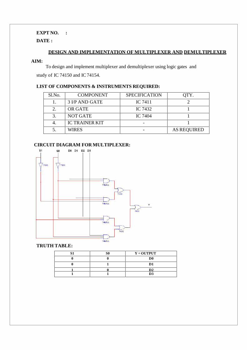
DESIGN AND IMPLEMENTATION OF MULTIPLEXER AND DEMULTIPLEXER
AIM:To design and implement multiplexer and demultiplexer using logic gates and
study of IC 74150 and IC 74154.
LIST OF COMPONENTS & INSTRUMENTS REQUIRED:
Sl.No. COMPONENT SPECIFICATION QTY.
1. 3 I/P AND GATE IC 7411 2
2. OR GATE IC 7432 1
3. NOT GATE IC 7404 14. IC TRAINER KIT - 1
5. WIRES - AS REQUIRED
CIRCUIT DIAGRAM FOR MULTIPLEXER:
TRUTH TABLE:
S1 S0 Y = OUTPUT0 0 D0
0 1 D1
1 0 D21 1 D3
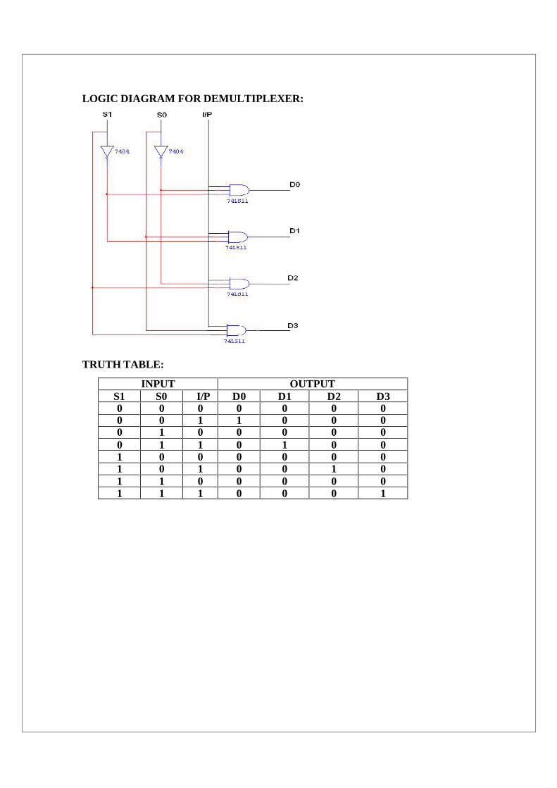
LOGIC DIAGRAM FOR DEMULTIPLEXER:
TRUTH TABLE:
INPUT OUTPUTS1 S0 I/P D0 D1 D2 D30 0 0 0 0 0 00 0 1 1 0 0 00 1 0 0 0 0 00 1 1 0 1 0 01 0 0 0 0 0 01 0 1 0 0 1 01 1 0 0 0 0 01 1 1 0 0 0 1

PROCEDURE:(i) Connections are given as per circuitdiagram.
(ii) Logical inputs are given as per circuit diagram.
(iii) Observe the output and verify the truth table.
RESULT:Thus the multiplexer and demultiplexer using logic gates was designed IC 74150
and IC 74154 also studied.
EXPT NO. :
DATE :
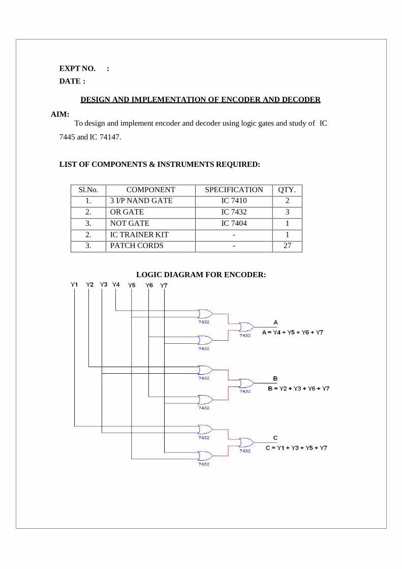
DESIGN AND IMPLEMENTATION OF ENCODER AND DECODER
AIM:To design and implement encoder and decoder using logic gates and study of IC
7445 and IC 74147.
LIST OF COMPONENTS & INSTRUMENTS REQUIRED:
Sl.No. COMPONENT SPECIFICATION QTY.1. 3 I/P NAND GATE IC 7410 2
2. OR GATE IC 7432 3
3. NOT GATE IC 7404 1
2. IC TRAINER KIT - 13. PATCH CORDS - 27
LOGIC DIAGRAM FOR ENCODER:

TRUTH TABLE FOR ENCODER:
INPUT OUTPUTY1 Y2 Y3 Y4 Y5 Y6 Y7 A B C1 0 0 0 0 0 0 0 0 10 1 0 0 0 0 0 0 1 00 0 1 0 0 0 0 0 1 10 0 0 1 0 0 0 1 0 00 0 0 0 1 0 0 1 0 10 0 0 0 0 1 0 1 1 00 0 0 0 0 0 1 1 1 1
LOGIC DIAGRAM FOR DECODER:
TRUTH TABLE FOR DECODER:
INPUT OUTPUT
E A B D0 D1 D2 D3
1 0 0 1 1 1 1
0 0 0 0 1 1 1
0 0 1 1 0 1 1
0 1 0 1 1 0 1
0 1 1 1 1 1 0

PROCEDURE:
(i) Connections are given as per circuitdiagram.
(ii) Logical inputs are given as per circuit diagram.
(iii) Observe the output and verify the truth table.
RESULT:Thus the encoder and decoder using logic gates were designed and IC 7445, IC
74147 was studied.
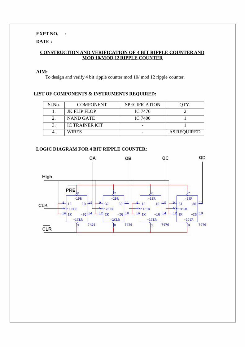
EXPT NO. :
DATE :
CONSTRUCTION AND VERIFICATION OF 4 BIT RIPPLE COUNTER ANDMOD 10/MOD 12 RIPPLE COUNTER
AIM:To design and verify 4 bit ripple counter mod 10/ mod 12 ripple counter.
LIST OF COMPONENTS & INSTRUMENTS REQUIRED:
Sl.No. COMPONENT SPECIFICATION QTY.1. JK FLIP FLOP IC 7476 2
2. NAND GATE IC 7400 1
3. IC TRAINER KIT - 14. WIRES - AS REQUIRED
LOGIC DIAGRAM FOR 4 BIT RIPPLE COUNTER:
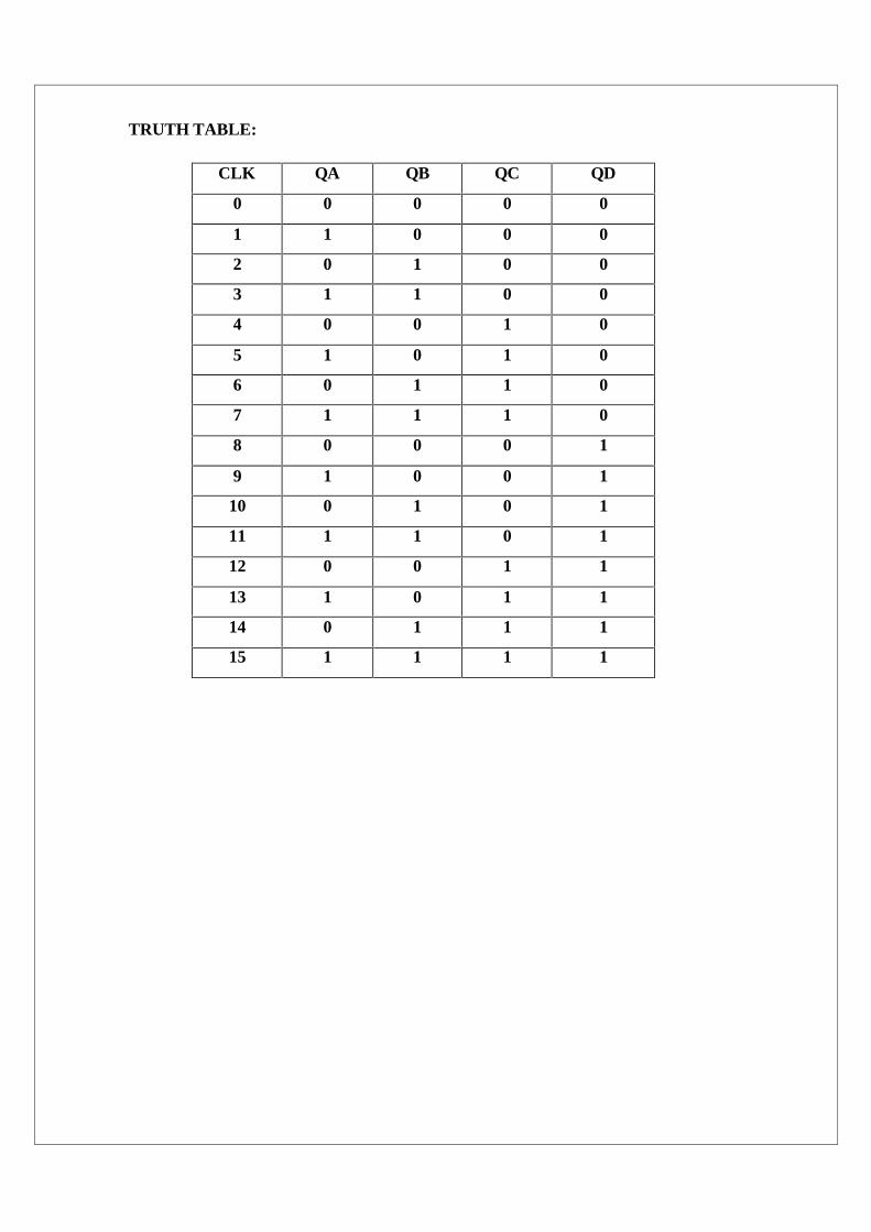
TRUTH TABLE:
CLK QA QB QC QD
0 0 0 0 0
1 1 0 0 0
2 0 1 0 0
3 1 1 0 0
4 0 0 1 0
5 1 0 1 0
6 0 1 1 0
7 1 1 1 0
8 0 0 0 1
9 1 0 0 1
10 0 1 0 1
11 1 1 0 1
12 0 0 1 1
13 1 0 1 1
14 0 1 1 1
15 1 1 1 1
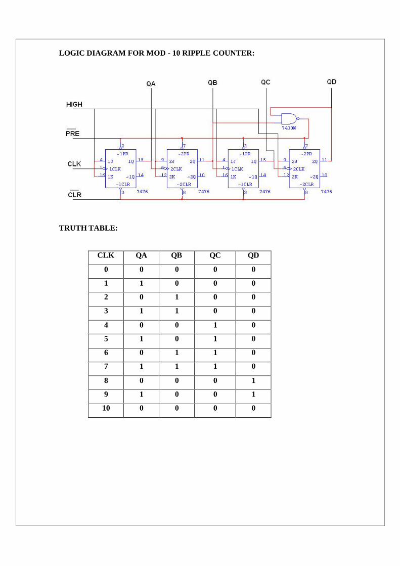
LOGIC DIAGRAM FOR MOD - 10 RIPPLE COUNTER:
TRUTH TABLE:
CLK QA QB QC QD
0 0 0 0 0
1 1 0 0 0
2 0 1 0 0
3 1 1 0 0
4 0 0 1 0
5 1 0 1 0
6 0 1 1 0
7 1 1 1 0
8 0 0 0 1
9 1 0 0 1
10 0 0 0 0
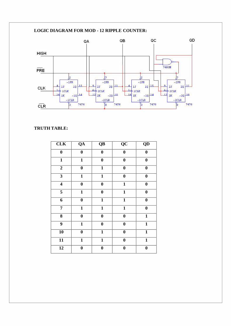
LOGIC DIAGRAM FOR MOD - 12 RIPPLE COUNTER:
TRUTH TABLE:
CLK QA QB QC QD
0 0 0 0 0
1 1 0 0 0
2 0 1 0 0
3 1 1 0 0
4 0 0 1 0
5 1 0 1 0
6 0 1 1 0
7 1 1 1 0
8 0 0 0 1
9 1 0 0 1
10 0 1 0 1
11 1 1 0 1
12 0 0 0 0

PROCEDURE:
(i) Connections are given as per circuitdiagram.
(ii) Logical inputs are given as per circuit diagram.
(iii) Observe the output and verify the truth table.
RESULT:
Thus the 4 bit ripple counter mod 10/ mod 12 ripple counters was implemented
and the truth table was verified.

EXPT NO. :
DATE :
DESIGN AND IMPLEMENTATION OF 3 BIT SYNCHRONOUS UP/DOWNCOUNTER
AIM: To design and implement 3 bit synchronous up/down counter
LIST OF COMPONENTS & INSTRUMENTS REQUIRED:
Sl.No. COMPONENT SPECIFICATION QTY.
1. JK FLIP FLOP IC 7476 22. 3 I/P AND GATE IC 7411 1
3. OR GATE IC 7432 1
4. XOR GATE IC 7486 1
5. NOT GATE IC 7404 16. IC TRAINER KIT - 1
7. WIRES - AS REQUIRED
LOGIC DIAGRAM:
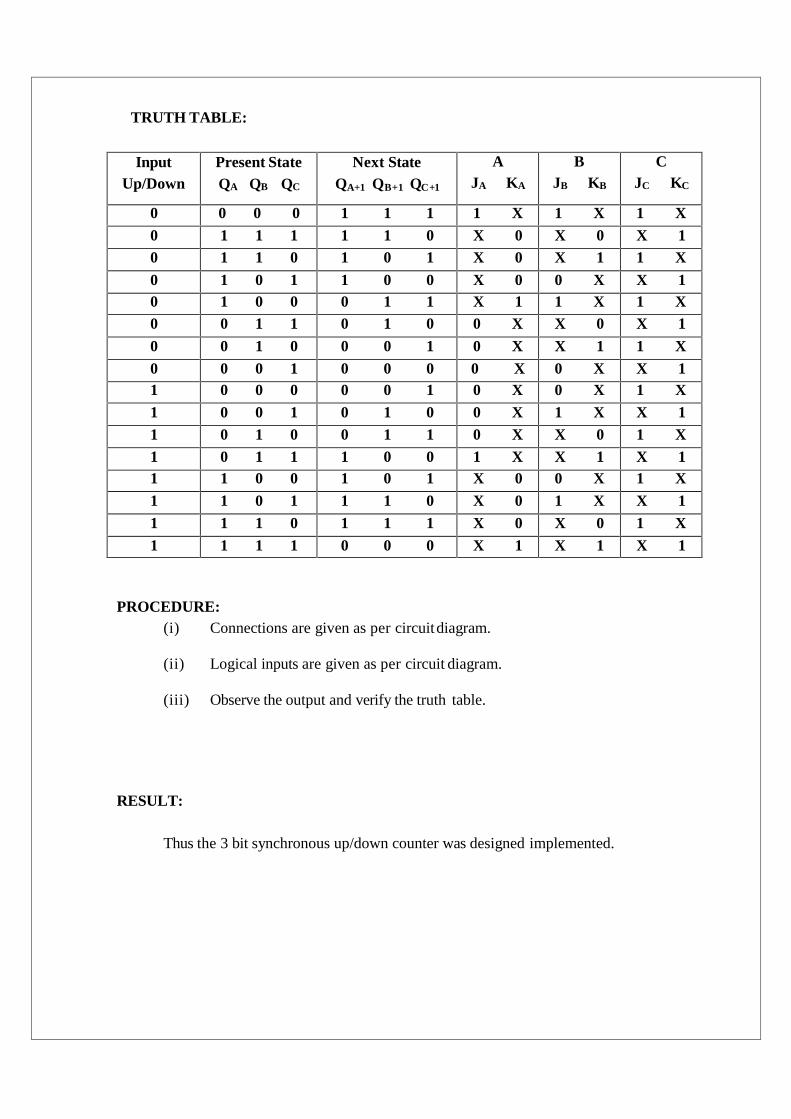
TRUTH TABLE:
InputUp/Down
Present StateQA QB QC
Next StateQA+1 QB+1 QC+1
AJA KA
BJB KB
CJC KC
0 0 0 0 1 1 1 1 X 1 X 1 X0 1 1 1 1 1 0 X 0 X 0 X 10 1 1 0 1 0 1 X 0 X 1 1 X
0 1 0 1 1 0 0 X 0 0 X X 10 1 0 0 0 1 1 X 1 1 X 1 X0 0 1 1 0 1 0 0 X X 0 X 1
0 0 1 0 0 0 1 0 X X 1 1 X0 0 0 1 0 0 0 0 X 0 X X 11 0 0 0 0 0 1 0 X 0 X 1 X1 0 0 1 0 1 0 0 X 1 X X 11 0 1 0 0 1 1 0 X X 0 1 X1 0 1 1 1 0 0 1 X X 1 X 11 1 0 0 1 0 1 X 0 0 X 1 X1 1 0 1 1 1 0 X 0 1 X X 11 1 1 0 1 1 1 X 0 X 0 1 X1 1 1 1 0 0 0 X 1 X 1 X 1
PROCEDURE:(i) Connections are given as per circuitdiagram.
(ii) Logical inputs are given as per circuit diagram.
(iii) Observe the output and verify the truth table.
RESULT:
Thus the 3 bit synchronous up/down counter was designed implemented.
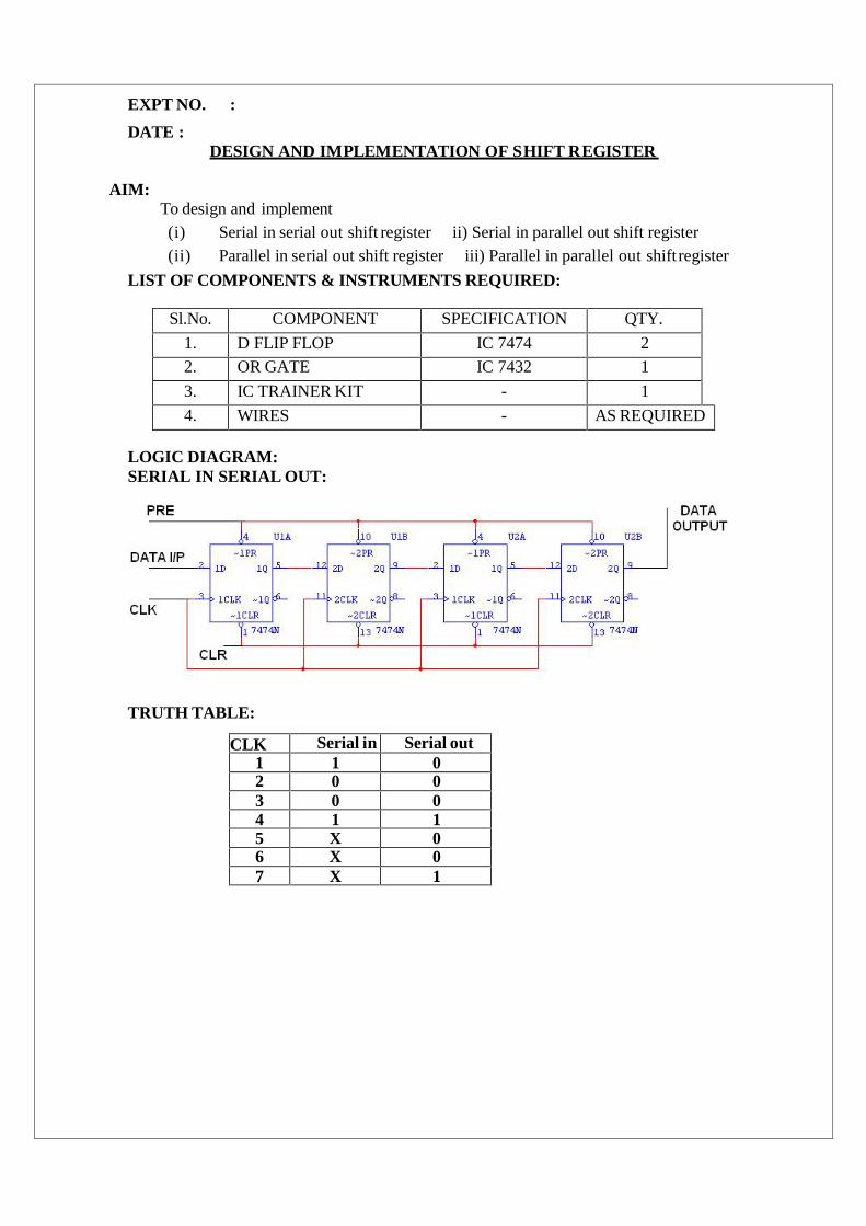
EXPT NO. :
DATE :DESIGN AND IMPLEMENTATION OF SHIFT REGISTER
AIM:To design and implement(i) Serial in serial out shift register ii) Serial in parallel out shift register(ii) Parallel in serial out shift register iii) Parallel in parallel out shift register
LIST OF COMPONENTS & INSTRUMENTS REQUIRED:
Sl.No. COMPONENT SPECIFICATION QTY.
1. D FLIP FLOP IC 7474 22. OR GATE IC 7432 1
3. IC TRAINER KIT - 1
4. WIRES - AS REQUIRED
LOGIC DIAGRAM:SERIAL IN SERIAL OUT:
TRUTH TABLE:
CLK Serial in Serial out1 1 02 0 03 0 04 1 15 X 06 X 07 X 1

LOGIC DIAGRAM:
SERIAL IN PARALLEL OUT:
TRUTH TABLE:
CLK DATA
OUTPUT
QA QB QC QD
1 1 1 0 0 02 0 0 1 0 03 0 0 0 1 14 1 1 0 0 1
LOGIC DIAGRAM: PARALLEL IN SERIAL OUT:
TRUTH TABLE:
CLK Q3 Q2 Q1 Q0 O/P0 1 0 0 1 11 0 0 0 0 02 0 0 0 0 03 0 0 0 0 1
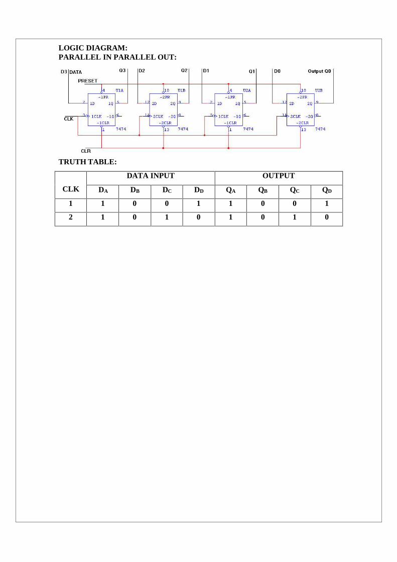
LOGIC DIAGRAM:PARALLEL IN PARALLEL OUT:
TRUTH TABLE:
CLK
DATA INPUT OUTPUT
DA DB DC DD QA QB QC QD
1 1 0 0 1 1 0 0 1
2 1 0 1 0 1 0 1 0

PROCEDURE:
(i) Connections are given as per circuitdiagram.
(ii) Logical inputs are given as per circuit diagram.
(iii) Observe the output and verify the truth table.
RESULT:
Thus the Serial in serial out, Serial in parallel out, Parallel in serial out andParallel in parallel out shift registers were implemented using IC 7474.

EXPT NO. :
DATE :BOOLEAN OPERATIONS USING LABVIEW
Aim: To perform Boolean operations using Labview.
Algorithm:
Step 1: Start the Labview and select the blank VI.
Step 2: Create front and block diagram panel.
Step 3: To perform Boolean operation push buttons are taken as inputs and round LED as output.
Step 4: Different Boolean operations such as AND, OR, XOR, NOT, NAND are
selected from the block diagram panel.
Step 5: Boolean inputs and outputs are wired in the block diagram panel.
Step 6: Logic values 0 & 1 are given in the front panel and the program is executed.
Block diagram:

RESULT:Thus the Boolean operation using LAB view is performed.

EXPT NAME: Design Entry and Simulation of Combinational Logic Circuits
DATE :
OBJECTIVE OF THE EXPERIMENTTo study about the simulation tools available in Xilinx project navigator using Verilog tools.
FACILITIES REQUIRED AND PROCEDUREa) Facilities required to do the experiment
S.No. SOFTWARE REQUIREMENTS Quantity1 Xilinx Project navigator – ISE 9.1 1
Procedure for doing the experimentNo Details of the step1 Double click the project navigator and select the option File-New project.2 Give the project name.3 Select Verilog module.4 Type your Verilog coding.5 Check for syntax.6 Select the new source of test bench waveform7 Choose behavioral simulation and simulate it by Xilinx ISE simulator.8 Verify the output.
c) Verilog coding:Logic gates:
AND GATE:module gl(a,b,c);input a;input b;output c;and(c,a,b);end module
OR GATE:module gl(a,b,c);input a;input b;output c;or(c,a,b);end module
XOR GATE:module gl(a,b,c);input a;input b;output c;xor (c,a,b);end module

NAND GATE:module gl(a,b,c);
input a;input b;output c;nand(c,a,b);end module
NOR GATE:module gl(a,b,c);input a;input b;output cnor(c,a,b);end module
HALF ADDER:module half adder(a,b,c,s);input a;input b;output c;output s;xor(s,a,b);and(c,~a,b);end module
HALF SUBTRACTOR:module half sub(a,b,c,s);input a;input b;
output c;output s;xor(s,a,b);and(c,~a,b);end module

ENCODERmodule Encd2to4(i0, i1, i2, i3, out0, out1);input i0,i1, i2, i3;output out0, out1;reg out0,out1;always@(i0,i1,i2,i3)case({i0,i1,i2,i3})4'b1000:{out0,out1}=2'b00;4'b0100:{out0,out1}=2'b01;4'b0010:{out0,out1}=2'b10;4'b0001:{out0,out1}=2'b11;default: $display("Invalid");endcaseendmodule
DECODER:// Module Name: Decd2to4module Decd2to4(i0, i1, out0, out1, out2, out3);input i0, i1;output out0, out1, out2, out3;reg out0,out1,out2,out3;always@(i0,i1)case({i0,i1})2'b00:{out0,out1,out2,out3}=4'b1000;2'b01:{out0,out1,out2,out3}=4'b0100;
2'b10:{out0,out1,out2,out3}=4'b0001;default:$display("Invalid");endcaseendmodule

MULTIPLEXER:// Module Name: Mux4to1module Mux4to1(i0, i1, i2, i3, s0, s1, out);input i0, i1, i2, i3, s0, s1;output out;wire s1n,s0n;wire y0,y1,y2,y3;not (s1n,s1);not (s0n,s0);and (y0,i0,s1n,s0n);and (y1,i1,s1n,s0);and (y2,i2,s1,s0n);and (y3,i3,s1,s0);or (out,y0,y1,y2,y3);endmodule
DEMULTIPLEXER:// Module Name: Dux1to4module Dux1to4(in, s0, s1, out0, out1, out2, out3);input in, s0, s1;output out0, out1, out2,out3;wire s0n,s1n;not(s0n,s0);not(s1n,s1);
and (out0,in,s1n,s0n);and (out1,in,s1n,s0);and (out2,in,s1,s0n);and (out3,in,s1,s0);endmodule
8 BIT ADDERmodule adder(a,b, s,c);input [7:0] a,b;output [7:0] s,c;assign {c,s} = a + b;endmodule
RESULT:Thus the program for study of simulation using tools and the output also verified
successfully.

EXPT NAME : IMPLEMENTATION OF FLIP-FLOPSDATE :
OBJECTIVE OF THE EXPERIMENTTo implement Flip-flops using Verilog HDL.
FACILITIES REQUIRED AND PROCEDURE
a) Facilities required to do the experimentS.No. SOFTWARE REQUIREMENTS Quantity
1 Xilinx Project navigator – ISE 9.1 1
b) Procedure for doing the experimentS.No Details of the step
1 Double click the project navigator and select the option File-New project.2 Give the project name.3 Select Verilog module.4 Type your verilog coding.5 Check for syntax.6 Select the new source of test bench waveform7 Choose behavioral simulation and simulate it by xilinx ISE simulator.8 Verify the output.
c) Verilog coding:
PROGRAM:
D Flip-Flop:// Module Name: DFFmodule DFF(Clock, Reset, d, q);input Clock;input Reset;input d;output q;reg q;always@(posedge Clock or negedge Reset)if (~Reset) q=1'b0;else q=d;endmodule

T Flip-Flop:// Module Name: TFFmodule TFF(Clock, Reset, t, q);input Clock;input Reset;input t;output q;reg q;always@(posedge Clock , negedge Reset)if(~Reset) q=0;else if (t) q=~q;else q=q;endmodule
JK Flip-Flop:Program:// Module Name: JKFFmodule JKFF(Clock, Reset, j, k, q);input Clock;input Reset;input j;input k;output q;reg q;always@(posedge Clock, negedge Reset)if(~Reset)q=0;elsebegincase({j,k})2'b00: q=q;2'b01: q=0;2'b10: q=1;2'b11: q=~q;endcaseendendmodule
RESULT:Thus the flip-flops program was implemented using tools and the output also verifiedsuccessfully.

EXPT NAME : IMPLEMENTATION OF COUNTERSDATE :
OBJECTIVE OF THE EXPERIMENTTo implement Counters using Verilog HDL.
FACILITIES REQUIRED AND PROCEDUREa) Facilities required to do the experiment
S.No. SOFTWARE REQUIREMENTS Quantity1 Xilinx Project navigator – ISE 9.1 1
b) Procedure for doing the experimentS.No Details of the step
1 Double click the project navigator and select the option File-New project.2 Give the project name.3 Select Verilog module.4 Type your verilog coding.5 Check for syntax.6 Select the new source of test bench waveform7 Choose behavioral simulation and simulate it by xilinx ISE simulator.8 Verify the output.
c) Verilog coding:PROGRAM:2- Bit Counter:// Module Name: Count2Bitmodule Count2Bit(Clock, Clear, out);input Clock;input Clear;output [1:0] out;reg [1:0]out;always@(posedge Clock, negedge Clear)if((~Clear) || (out>=4))out=2'b00;else out=out+1;endmodule
RESULT:Thus the counters program was implemented using tools and the output also verified
successfully.

IMPLEMENTATION OF BASIC LOGIC GATES
1(a)OR GATEAIM: Design &Simulate a logic circuit of OR gate
COMPONENTS USED: OR gate(7432N)
2 clock voltage
2dig probe bulb
1dig probe green bulb
2DGND
THEORY:
The OR gate performs logical addition,more commonly known as the ‘OR’ function.An OR gate has two or more inputs and one output as indicated by the standard logic symbolas shown in fig
PROCEDURE:
Open Multisim,click on file, select new-schematic capture.
Click on ‘Place’,click Component, select aComponent window opens & select the
following
Select TTL,74STD,OR gate(74s32) & click ok.
Pick and place the OR gate on the screen.
Select Sources, Signal Sources,Clock voltage & click ok.
Place 2 clock voltages on the screen(for 2 inputs).
Select Sources, Power source,DGND( ground)& click ok.
Place 2 DGND on the screen(for 2 inputs).
Select Indicators,Probe, Dig Probe, Red indicator bulb & click ok.
Place 2 Dig Probe Red bulb on the screen.(for 2 inputs).
Select Indicators, Probe,Dig probe Green indicator bulb & click ok.
Place 1 Dig Probe Green bulb on the screen.(for 1 output).
Now join the circuit as shown in fig.
Run/Simulate the circuit using simulation bar.

Result:Design of logic circuit of OR gate is completed. Simulation of logic circuit OR gate
satisfies the truth table.

1(b) AND GATEAIM:
Design &simulate a logic circuit of OR gate
COMPONENTS USED: ANDgate (7408J)
2 clock voltage
2dig probe red bulbs
1dig probe green bulb
2DGND
THEORY:The AND gate performs logical multiplication, more commonly known as the AND
function. The AND gate may have two or more inputs and a single output, as indicated by thestandard logic symbols shown in the fig.
PROCEDURE:
Open Multisim,click on file, select new-schematic capture.
Click on Place,click Component, select aComponent window opens & select the
following
Select TTL,74STD,ANDgate(7408J) & click ok.
Place the AND gate on the screen.
Select Sources, Signal, sources, Clock voltage & click ok.
Place 2 Clock voltages on the screen(for 2 inputs).
Select Sources, Power source,DGND & click ok.
Place 2 DGND on the screen(for 2 inputs).
Select Indicators,Probe,Dig probe red bulb & click ok.
Place 2 dig probe red bulb on the screen.(for 2 inputs).
Select Indicators, Probe, Dig probe green bulb & click ok.
Place 1 dig probe green bulb on the screen.(for 1 output).
Now join the circuit as shown in fig.
Run/Simulate the circuit using simulation bar.

RESULT:Design of logic circuit of AND gate is completed. Simulation of logic circuit AND gate
satisfies the truth table.

1(c) NOT GATEAIM:
Design & Simulate a logic circuit of NOT gate
COMPONENTS USED: NOTgate (7404N)
2 clock voltage
2Dig probe red bulbs
1Dig probe green bulb
2DGND
THEORY:A NOT gate produces an output that is a complement of the input. It has only one input
signal and one output signal as indicated by the logic symbol as shown in fig.
PROCEDURE:
Open Multisim, click on file, select new-schematic capture.
Click on Place, clickComponent, selecta Component window opens & select the
following
Select TTL, 74STD, NOT gate(7404N) & click ok.
Place the NOT gate on the screen.
Select Sources, Signal Sources,Clock voltage & click ok.
Place 1 clock voltages on the screen(for 1inputs).
Select Sources, Power source,DGND & click ok.
Place 1 DGND on the screen (for 1 input).
Select Indicators,Probe,Dig probe red bulb & click ok.
Place 1 dig probe red bulb on the screen. (for 1 inputs).
Select Indicators, Probe, Dig probe green bulb & click ok.
Place 1 dig probe green bulb on the screen.(for 1 output).
Now join the circuit as shown in fig.
Run/Simulate the circuit using simulation bar.
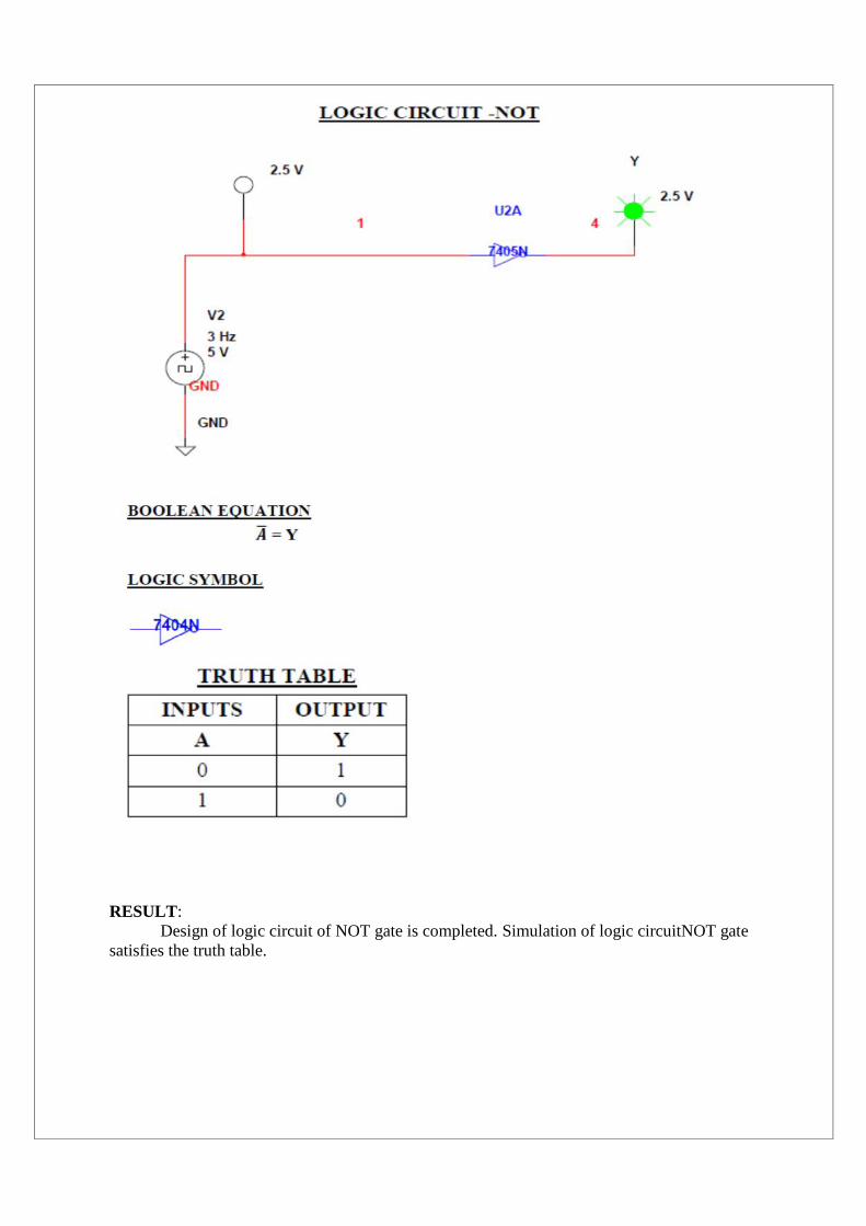
RESULT:Design of logic circuit of NOT gate is completed. Simulation of logic circuitNOT gate
satisfies the truth table.

1(d) NOR GATEAIM:
Design &Simulate a logic circuit of NOR gate
COMPONENTS USED: NOR gate(7402N)
2 clock voltage
2dig probe red bulbs
1dig probe green bulb
2DGND
THEORY:The term NOR is a contraction of NOT-OR and implies an OR function with an
inverted (compliment) output.A standard logic symbol for two inputs NOR gate is as shown infig.
PROCEDURE: Open Multisim, click on file, select new-schematic capture.
Click on Place, click Component, select a Component window opens & select the
following
Select TTL,74STD,NOR gate(7402N) & click ok.
Place the NOR gate on the screen.
Select Sources, Signal sources, Clock voltage & click ok.
Place 2 clock voltages on the screen(for 2 inputs).
Select Sources, Power source,DGND & click ok.
Place 2 DGND on the screen(for 2 inputs).
Select Indicators,Probe,Dig probe red bulb & click ok.
Place 2 dig probe red bulb on the screen (for 2 inputs).
Select Indicators,probe, Dig probe green bulb & click ok.
Place 1 dig probe green bulb on the screen.(for 1 output).
Now join the circuit as shown in fig.
Run/Simulate the circuit using simulation bar.
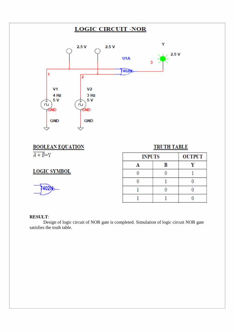
RESULT:Design of logic circuit of NOR gate is completed. Simulation of logic circuit NOR gate
satisfies the truth table.

1(e) NAND GATEAIM:
Design & Simulate a logic circuit of NAND gate
COMPONENTS USED: NANDgate(7400N)
2 Clock voltage
2Dig probe red bulbs
1Dig probe green bulb
2DGND
THEORY:The term NAND is a contraction of NOT-AND and implies an AND function with a
complement (inverted) output. A standard logic symbol for 2-input NAND gate is as shown infig.
PROCEDURE:
Open Multisim, Click on file, select new-schematic capture.
Click on Place, click Component, select a Component window opens & select the
following
Select TTL,74STD,NANDgate(7400N) & click ok.
Place the NAND gate on the screen.
Select Sources, Signal sources, Clock voltage & click ok.
Place 2 clock voltages on the screen(for 2 inputs).
Select Sources, Power source,DGND & click ok.
Place 2 DGND on the screen(for 2 inputs).
Select Indicators,Probe,Dig probe red bulb & click ok.
Place 2 dig probe red bulb on the screen.(for 2 inputs).
Select Indicators, Probe, Dig probe green bulb & click ok.
Place 1 dig probe green bulb on the screen.(for 1 output).
Now join the circuit as shown in fig.
Run/Simulate the circuit using simulation bar.
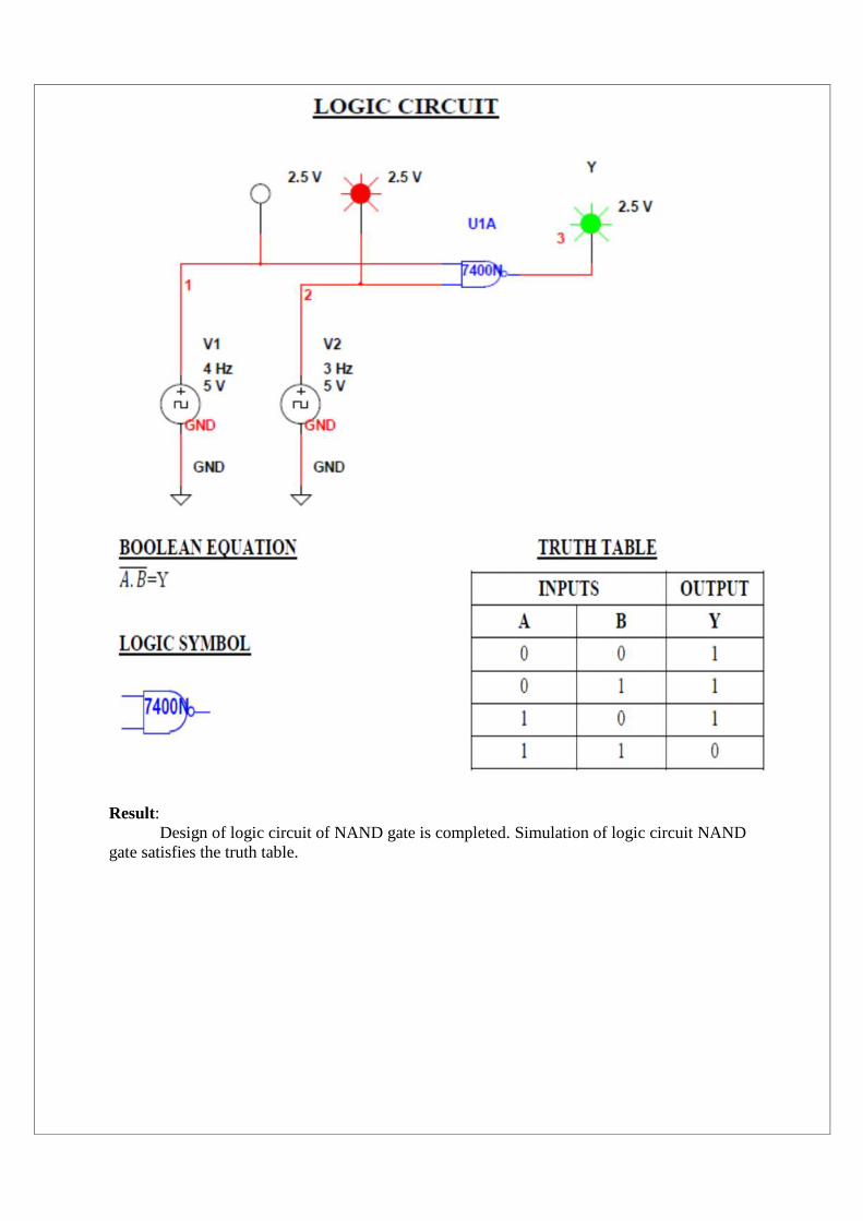
Result:Design of logic circuit of NAND gate is completed. Simulation of logic circuit NAND
gate satisfies the truth table.

1(f) X-OR GATEAIM:
Design &simulate a logic circuit of X-OR gate
COMPONENTS USED: X-OR gate(7432N)
2 Clock voltage
2Dig probe red bulbs
1Dig probe green bulb
2DGND
THEORY:The X-OR is an abbreviation for Exclusive-OR gate. An X-OR gate has two or more
inputs and one output as indicated by the standard logic symbol as shown in fig.
PROCEDURE:
Open Multisim,click on file, select new-schematic capture.
Click on Place, click Component, select a Component window opens & select the
following
Select TTL,74STD,X-OR gate(7486N) & click ok.
Place the OR gate on the screen.
Select Sources, signal sources, Clock voltage & click ok.
Place 2 clock voltages on the screen(for 2 inputs).
Select Sources, Power source, DGND & click ok.
Place 2 DGND on the screen(for 2 inputs).
Select Indicators, Probe, Dig probe red bulb & click ok.
Place 2 dig probe red bulb on the screen.(for 2 inputs).
Select Indicators, probe, dig probe green bulb & click ok.
Place 1 dig probe green bulb on the screen.(for 1 output).
Now join the circuit as shown in fig.
Run/Simulate the circuit using simulation bar.
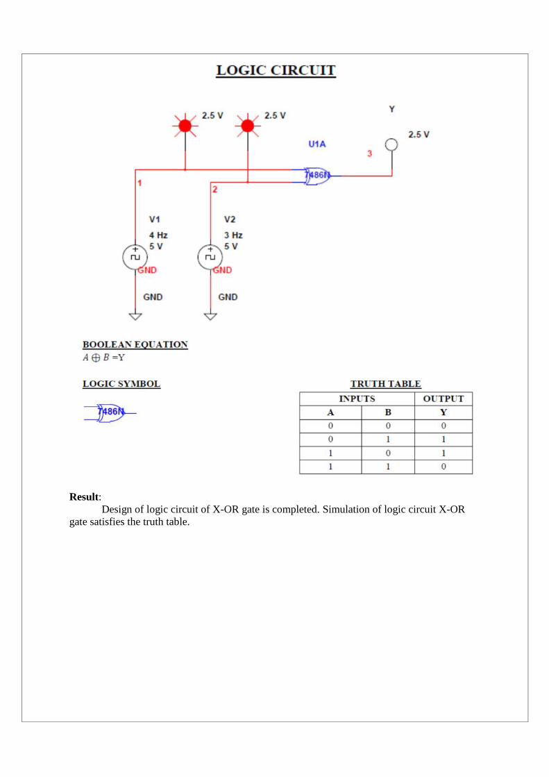
Result:Design of logic circuit of X-OR gate is completed. Simulation of logic circuit X-OR
gate satisfies the truth table.

1(g) X-NOR GATEAIM:
Design & simulate a logic circuit of X-NOR gate
COMPONENTS USED: XOR gate(7486N)
NOT gate(7405N)
2 clock voltage
2dig probe red bulbs
1dig probe green bulb
2DGND
THEORY:An Exclusive-NOR(X-NOR) gate is a coincidence gate. It produces one output only
when its two inputs are equal, i.e., when both inputs are either zero or one.
PROCEDURE: Open Multisim, click on file, select new-schematic capture.
Click on Place, click Component, select a component window opens & select the
following
Select TTL, 74STD, X-OR gate(7486N),NOT(7405N)& click ok.
Place the X-OR gate, NOT gate on the screen.
Select Sources, Signal sources, Clock voltage & click ok.
Place 2 clock voltages on the screen (for 2 inputs).
Select Sources, Power source, DGND & click ok.
Place 2 DGND on the screen(for 2 inputs).
Select Indicators, Probe, Dig probe red bulb & click ok.
Place 2 dig probe red bulb on the screen.(for 2 inputs).
Select Indicators, probe, Dig probe green bulb & click ok.
Place 1 dig probe green bulb on the screen.(for 1 output).
Now join the circuit as shown in fig.
Run/Simulate the circuit using simulation bar.
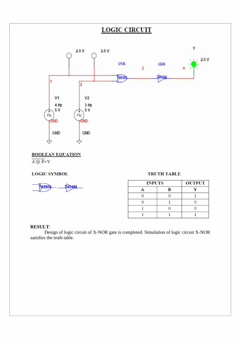
RESULT:Design of logic circuit of X-NOR gate is completed. Simulation of logic circuit X-NOR
satisfies the truth table.

2. COMBINATION OF GATES
2(a) HALF ADDER
AIM:Design & Simulate a logic circuit of half adder.
COMPONENTS USED: One XOR gate(7486N),
one AND gate(7408J),
2 clock voltage,
2 dig probe red bulb,
2 dig probe green bulb,
2 DGND
THEORY:The half adder circuit adds two binary digits & produces a sum (Σ) & a carry output
(Co).In other words, the binary arithmetic operation (A+B) produces (Σ) .
PROCEDURE:
Open Multisim, click on file, select new-schematic capture.
Click on Place, click Component, select a component window opens & perform the
following
Place XOR gate(7486N), one AND gate(7408J),2 clock voltage,2 dig probe red bulb,2
dig probe green bulb,2 DGND on the screen.
Join the circuit as shown in fig.
Run/Simulate the circuit.
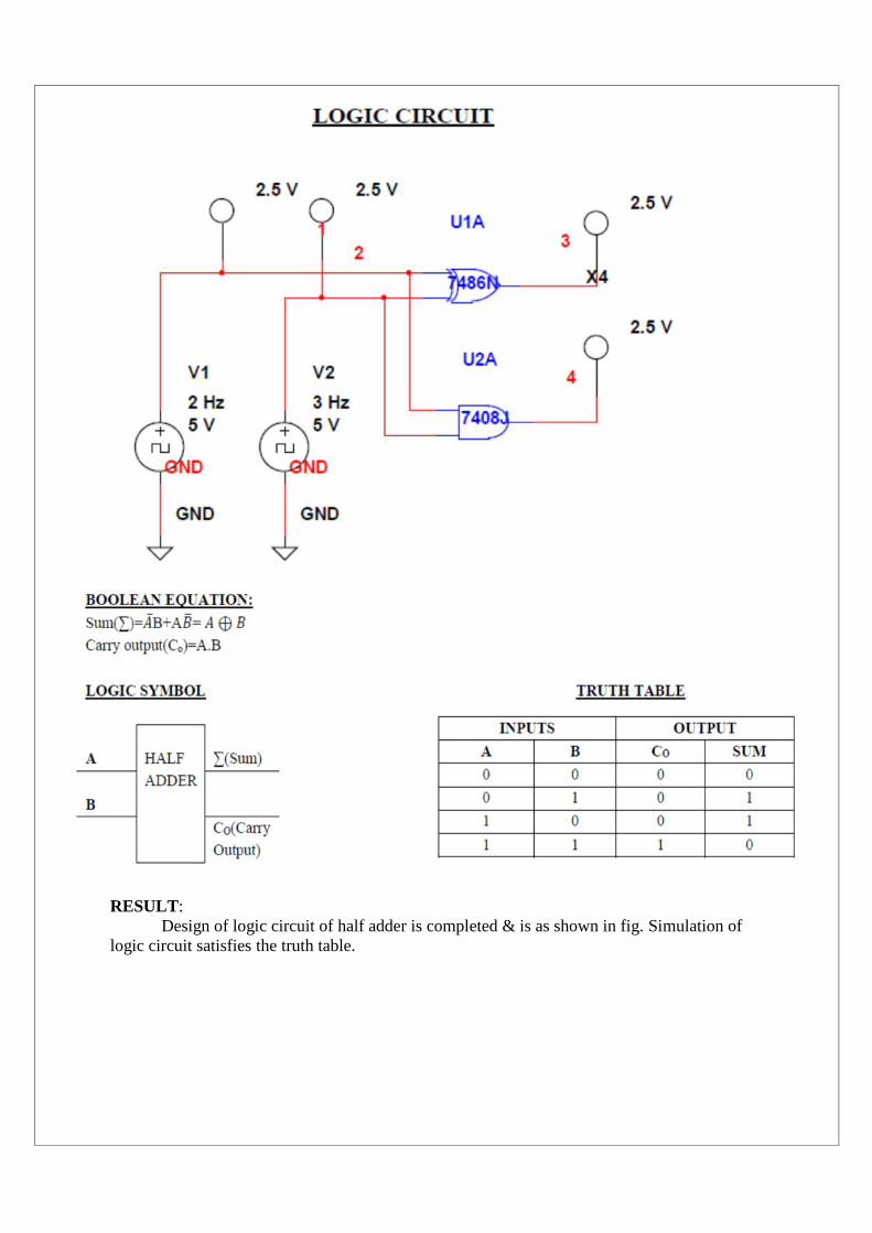
RESULT:Design of logic circuit of half adder is completed & is as shown in fig. Simulation of
logic circuit satisfies the truth table.

2(b) FULL ADDER
AIM:Design & Simulate a logic circuit of full adder.
COMPONENTS USED:
2 XOR gate(7486N),
2 AND gate(7408J),
one OR gate(7132N)
3 clock voltage
3 dig probe red bulb
2 dig probe green bulb
3 DGND
THEORY:The full adder adds the bits A & B &Carry (Ci) from the previous column. It generates
a sum (Σ) and a Carry output (CO).The basic difference between a full adder & a half adder isthat the full adder accepts an additional input.
PROCEDURE: Open Multisim, click on file, select new-schematic capture.
Click on Place, click Component, select a Component window opens & perform the
following
Place X-OR gate(7486N), one AND gate(7408J),2 clock voltage,2 dig probe red
bulbs,2 dig probe green bulbs,2 DGND on the screen.
Join the circuit as shown in fig.
Run/Simulate the circuit.
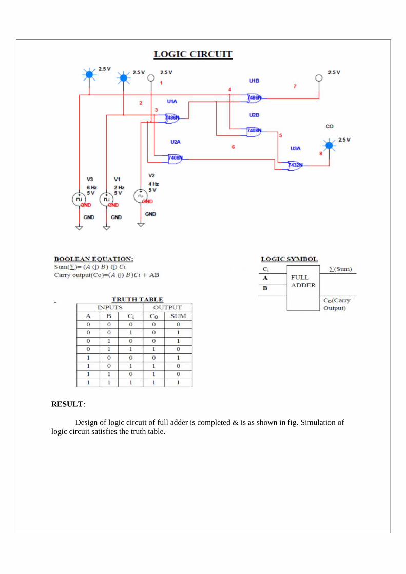
RESULT:
Design of logic circuit of full adder is completed & is as shown in fig. Simulation oflogic circuit satisfies the truth table.

2(c) HALF SUBTRACTOR
AIM:Design & Simulate a logic circuit of half subtractor.
COMPONENTS USED:
One X-OR gate(7486N)
one AND gate(7408J)
one NOT gate(7404N)
2 clock voltage
2 dig probe red bulb
2 dig probe green bulb
2 DGND
THEORY:A half Subtractor is an arithmetic circuit that subtracts one bit from another bit,
producing a difference bit (D) and borrow bit (Bo).
PROCEDURE:
Open Multisim,click on file, select new-schematic capture.
Click on Place, click Component, select a Component window opens & perform the
following
Place one X-OR gate(7486N), one AND gate(7408J), one NOT gate(7404N),2 clock
voltage,2 dig probe red bulb,2 dig probe green bulb,2 DGND on the screen.
Join the circuit as shown in fig.
Run/Simulate the circuit.

RESULT:Design of logic circuit of half subtractor is completed. Simulation of logic circuit
satisfies the truth table shown.

2(d) FULL SUBTRACTOR
AIM:Design & Simulate a logic circuit of full subtractor.
COMPONENTS USED: One X-OR gate(7486N)
one AND gate(7408J)
one NOT gate(7404N)
2 clock voltage
2 dig probe red bulb
2 dig probe green bulb
2 DGND
THEORY:It is an arithmetic circuit that subtracts one bit (subtrahend) from another bit (minuend)
taking into consideration the borrow (Bo) from the column. It produces a difference bit (D) anda borrow bit (Bo) required for the next higher column.
PROCEDURE:
Open Multisim, click on file, select new-schematic capture.
Click on Place, click Component, select a Component window opens & perform the
following
Place one X-OR gate(7486N), one AND gate(7408J), one NOT gate(7404N),2 clock
voltage,2 dig probe red bulb,2 dig probe green bulb,2 DGND on the screen.
Join the circuit as shown in fig.
Run/Simulate the circuit.
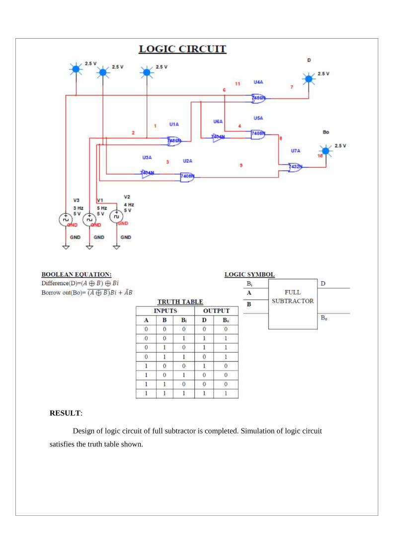
RESULT:
Design of logic circuit of full subtractor is completed. Simulation of logic circuit
satisfies the truth table shown.

3. DECODERS & ENCODERS
3(a) 2-4 DECODER
AIM:Design & Simulate a logic circuit of 2-4 decoders.
COMPONENTS USED:
Four AND gate(7408J)
two NOT gate(7404N)
2 clock voltage
2 dig probe red bulb
4 dig probe green bulb
2 DGND
THEORY:A decoder is a logic circuit that looks at its inputs, determines which number is there and
activates the one output that corresponds to that number.2-4 decoders are used where a decoderhas two input lines and four output lines. It takes a two bit binary number and activates any oneof the four outputs corresponding to that number.
PROCEDURE:
Open Multisim, click on file, select new-schematic capture.
Click on Place, click Component, select a Component window opens & perform the
following
Place Four AND gate(7408J), two NOT gate(7404N), 2 clock voltage, 2 dig probe red
bulb,4 dig probe green bulb, 2 DGND on the screen.
Join the circuit as shown in fig.
Run/Simulate the circuit.

RESULT:Design of logic circuit of 2-4 decoder is completed. Simulation of logic circuit satisfies
the truth table shown.

3(b) 3-8 DECODER
AIM:Design & Simulate a logic circuit of 3-8 decoder.
COMPONENTS USED:
Eight AND gate(7408J)
three NOT gate(7404N)
3 clock voltage
3 dig probe red bulb
8 dig probe green bulb
3 DGND
THEORY:
A decoder is a logic circuit that looks at its inputs, determines which number is there,and activates the output that corresponds to that number.3-8 decoders are used where a decoderhas three input lines and eight output lines. It takes a three bit binary number and activates anyone of the eight outputs corresponding to that number.
PROCEDURE:
Open Multisim, click on file, select new-schematic capture.
Click on Place, click Component,select aComponent window opens & perform the
following
Place eight AND gate(7408J), three NOT gate(7404N), 3 clock voltage, 3 dig probe red
bulb,8 dig probe green bulb, 3 DGND on the screen.
Join the circuit as shown in fig.
Run/Simulate the circuit.
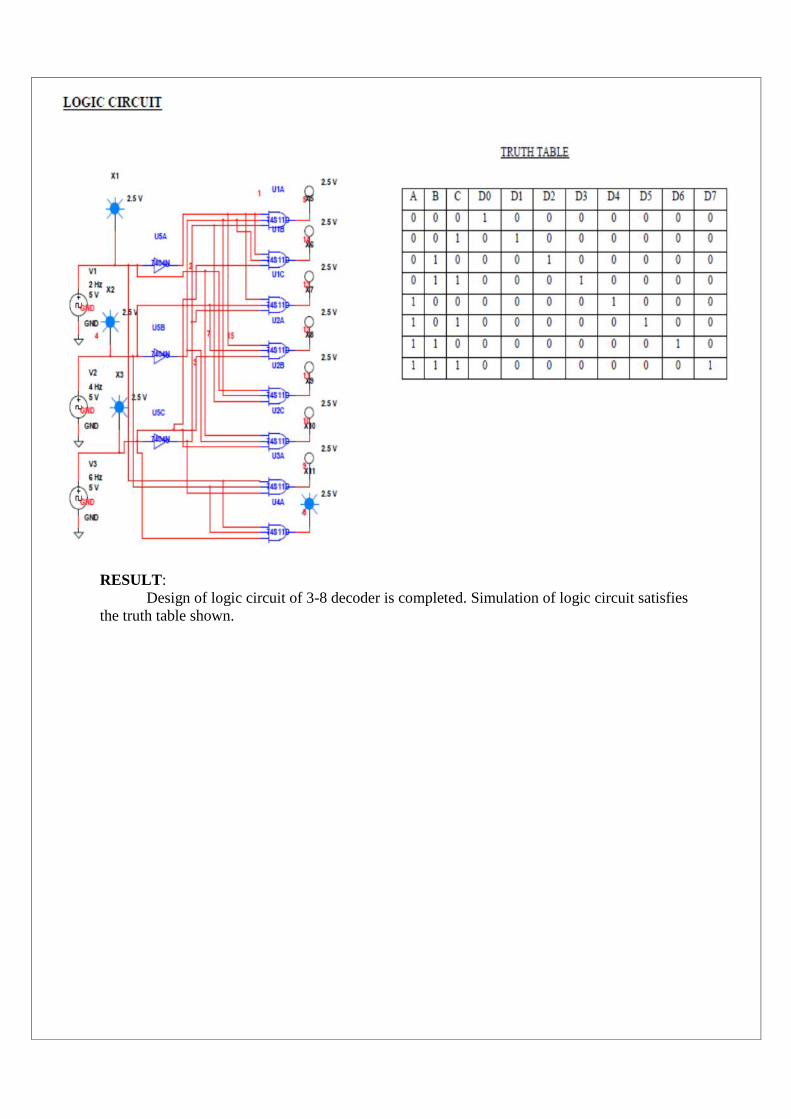
RESULT:Design of logic circuit of 3-8 decoder is completed. Simulation of logic circuit satisfies
the truth table shown.

5. FLIP FLOP
5(a) S-R FLIP FLOPAIM:
Design & Simulate a logic circuit of S-R Flip flop.
COMPONENTS USED:
Two NOT gate(7416N)
two NAND gate(7402N)
2 clock voltage
2 dig probe red bulb
2 dig probe green bulb
2 DGND
THEORY:The S-R Flip Flop using two NAND gates as shown in fig. The two NAND gates are
cross coupled, so that the output of NAND gate 1 is connected to one of the inputs of NANDgate 2 and vice versa. The Flip Flop has two outputs Q and and two inputs Set and Reset.
PROCEDURE:
Open Multisim, click on file, select new-schematic capture.
Click on Place, click Component, select a Component window opens & perform the
following
Place Two NOT gate(7416N),two NAND gate(7402N), 2 clock voltage, 2 dig probe
red bulb,2 dig probe green bulb, 2 DGND on the screen.
Join the circuit as shown in fig.
Run/Simulate the circuit.
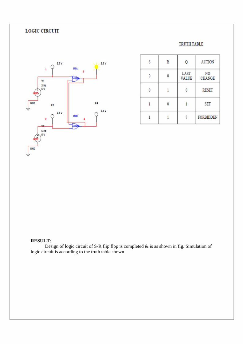
RESULT:Design of logic circuit of S-R flip flop is completed & is as shown in fig. Simulation of
logic circuit is according to the truth table shown.

5(b) J-K FLIP FLOPAIM:
Design & Simulate a logic circuit of J-K Flip flop.
COMPONENTS USED:
JK Flip Flop
Two SPDT Switch
Function generator
Two Indicator Probes
2 dig probe green bulb
2 DGND
THEORY:The J-K Flip Flop shown in fig.. The Flip Flop has two outputs Q and and two inputs
Set and Reset.
PROCEDURE:
Open Multisim, click on file, select new-schematic capture.
Click on Place, click Component, select a Component window opens & perform the
following
Place the above components
Join the circuit as shown in fig.
Run/Simulate the circuit.

J-K FLIP FLOP LOGIC DIAGRAM
RESULT:Design of logic circuit of J-K flip flop is completed & is as shown in fig. Simulation of logic
circuit is according to the truth table shown
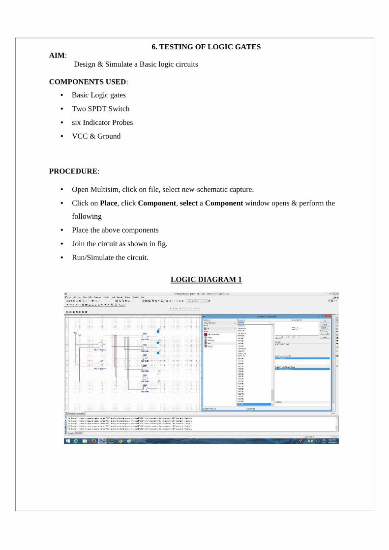
6. TESTING OF LOGIC GATESAIM:
Design & Simulate a Basic logic circuits
COMPONENTS USED:
Basic Logic gates
Two SPDT Switch
six Indicator Probes
VCC & Ground
PROCEDURE:
Open Multisim, click on file, select new-schematic capture.
Click on Place, click Component, select a Component window opens & perform the
following
Place the above components
Join the circuit as shown in fig.
Run/Simulate the circuit.
LOGIC DIAGRAM 1
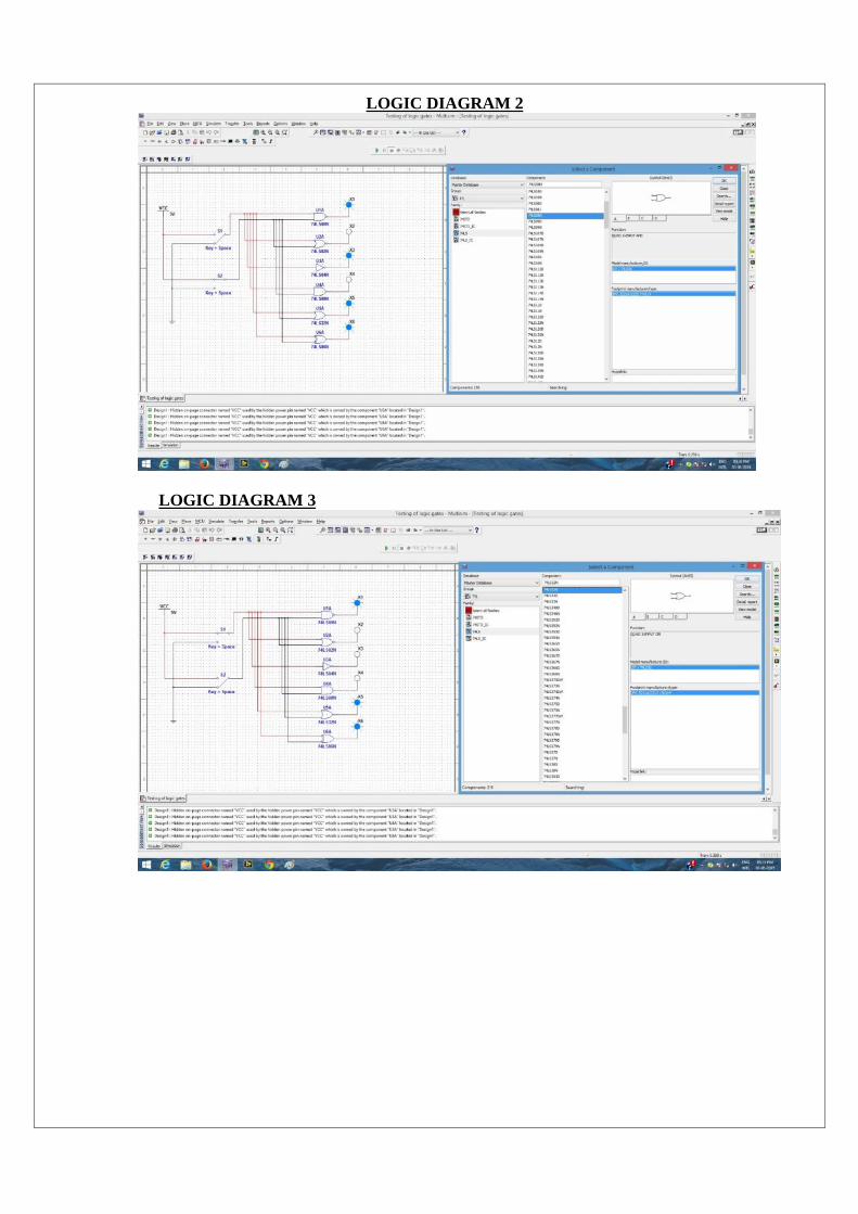
LOGIC DIAGRAM 2
LOGIC DIAGRAM 3
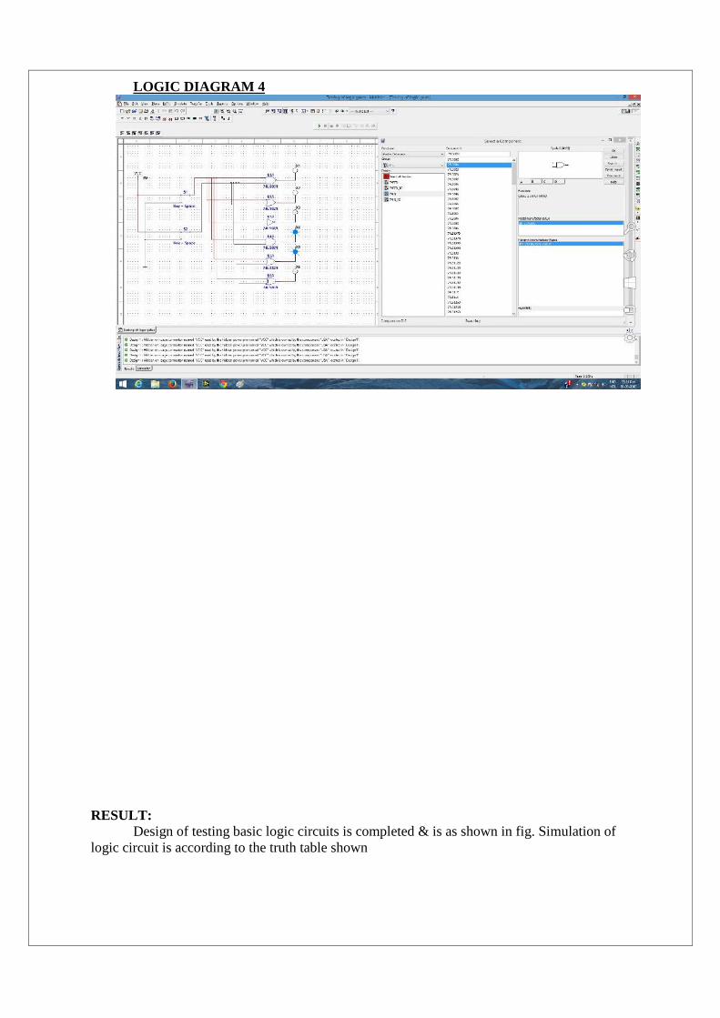
LOGIC DIAGRAM 4
RESULT:Design of testing basic logic circuits is completed & is as shown in fig. Simulation of
logic circuit is according to the truth table shown

7. 4X1 MULTIPLEXERAIM:
Design & Simulate a 4X1 Multiplexer
COMPONENTS USED:
Two 74LS04N, Four 74LS11N, One 4 Input OR gate
SIX SPDT Switch
Indicator Probe
VCC & Ground
PROCEDURE:
Open Multisim, click on file, select new-schematic capture.
Click on Place, click Component, select a Component window opens & perform the
following
Place the above components & Join the circuit as shown in fig.
Run/Simulate the circuit.
LOGIC DIAGRAM OF 4X1 MUX – EQUATION & TRUTH TABLE
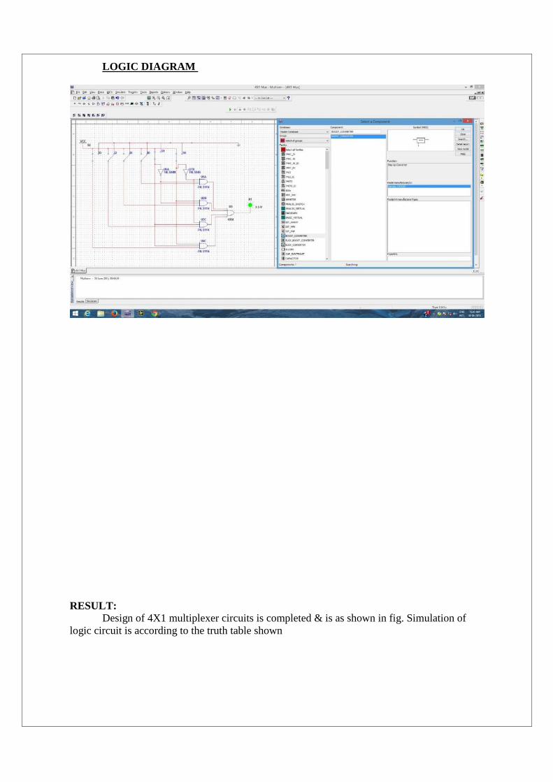
LOGIC DIAGRAM
RESULT:Design of 4X1 multiplexer circuits is completed & is as shown in fig. Simulation of
logic circuit is according to the truth table shown
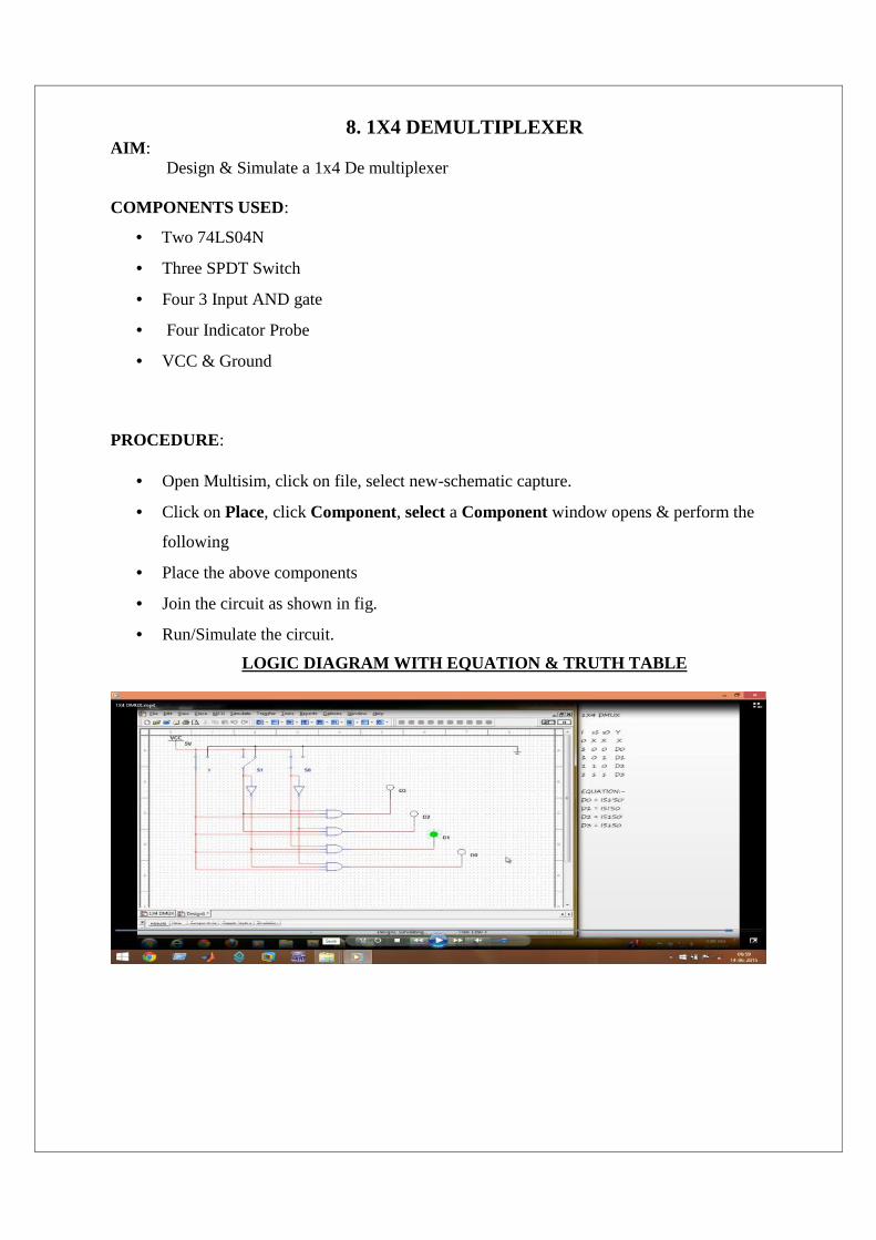
8. 1X4 DEMULTIPLEXERAIM:
Design & Simulate a 1x4 De multiplexer
COMPONENTS USED:
Two 74LS04N
Three SPDT Switch
Four 3 Input AND gate
Four Indicator Probe
VCC & Ground
PROCEDURE:
Open Multisim, click on file, select new-schematic capture.
Click on Place, click Component, select a Component window opens & perform the
following
Place the above components
Join the circuit as shown in fig.
Run/Simulate the circuit.
LOGIC DIAGRAM WITH EQUATION & TRUTH TABLE
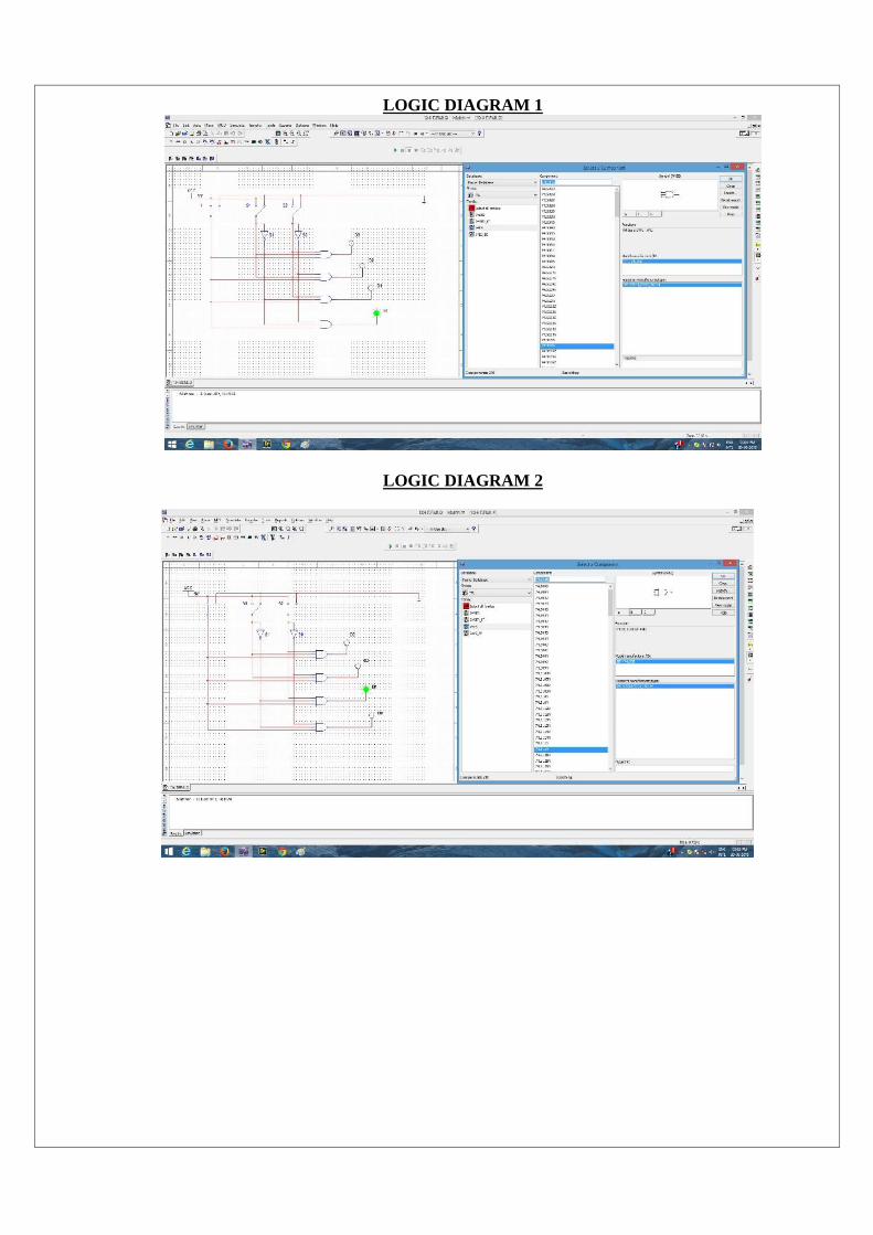
LOGIC DIAGRAM 1
LOGIC DIAGRAM 2
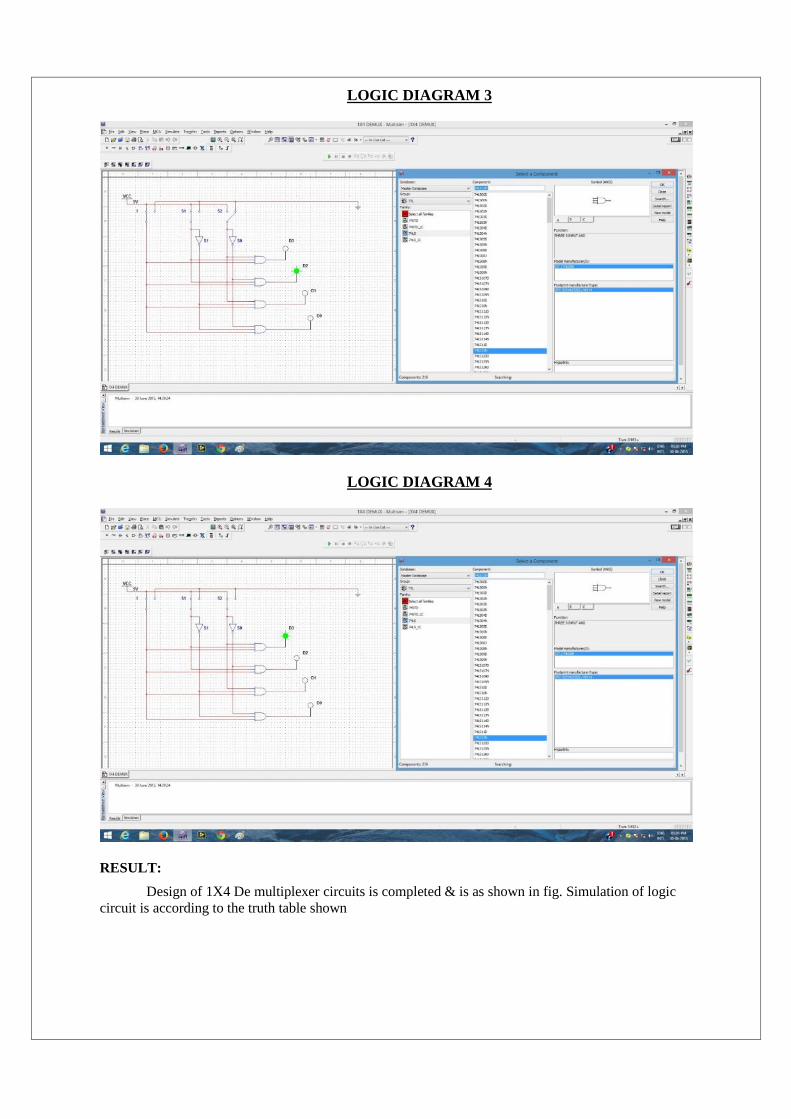
LOGIC DIAGRAM 3
LOGIC DIAGRAM 4
RESULT:
Design of 1X4 De multiplexer circuits is completed & is as shown in fig. Simulation of logiccircuit is according to the truth table shown
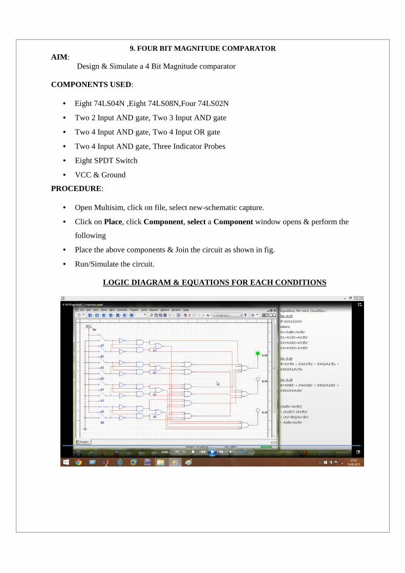
9. FOUR BIT MAGNITUDE COMPARATORAIM:
Design & Simulate a 4 Bit Magnitude comparator
COMPONENTS USED:
Eight 74LS04N ,Eight 74LS08N,Four 74LS02N
Two 2 Input AND gate, Two 3 Input AND gate
Two 4 Input AND gate, Two 4 Input OR gate
Two 4 Input AND gate, Three Indicator Probes
Eight SPDT Switch
VCC & Ground
PROCEDURE:
Open Multisim, click on file, select new-schematic capture.
Click on Place, click Component, select a Component window opens & perform the
following
Place the above components & Join the circuit as shown in fig.
Run/Simulate the circuit.
LOGIC DIAGRAM & EQUATIONS FOR EACH CONDITIONS
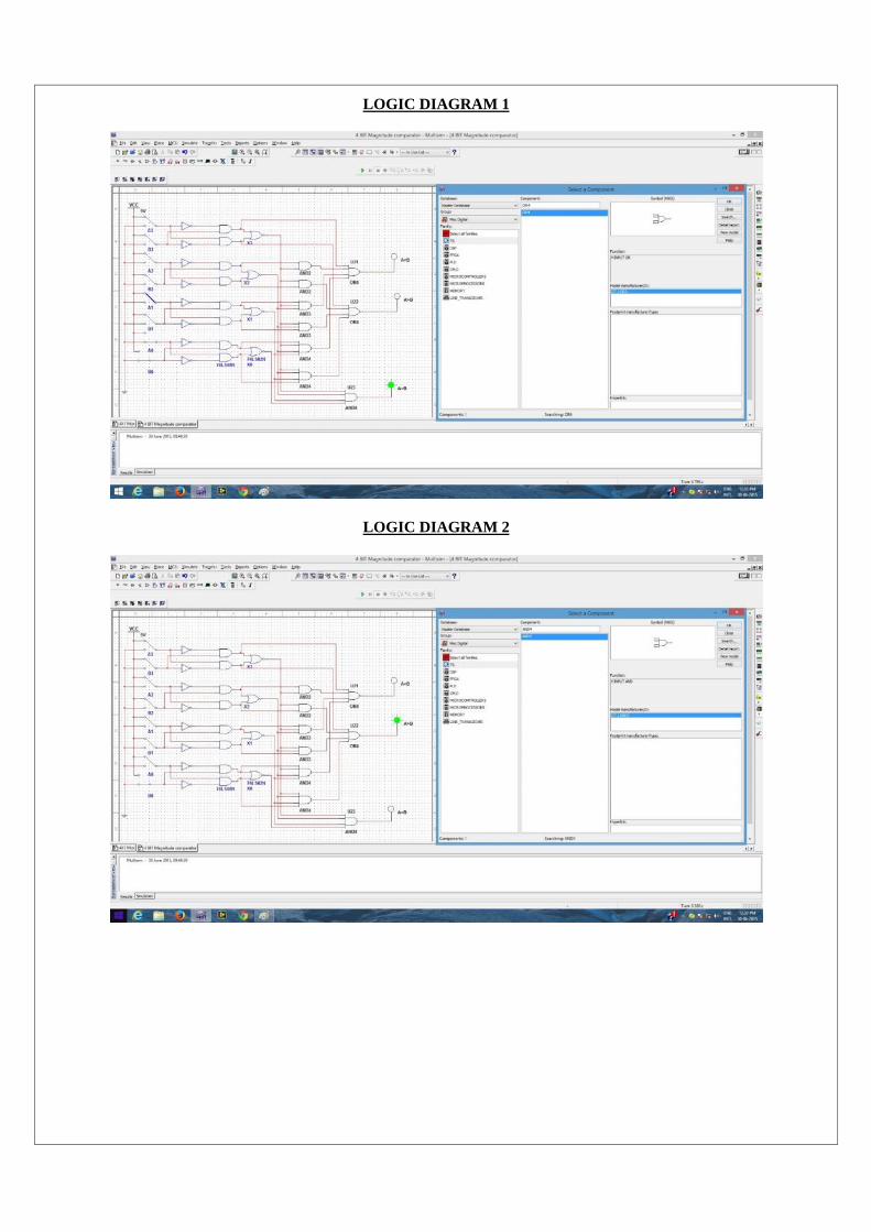
LOGIC DIAGRAM 1
LOGIC DIAGRAM 2

LOGIC DIAGRAM 3
RESULT:Design of 4 Bit Magnitude Comparator circuit is completed & is as shown in fig.
Simulation of logic circuit is according to the truth table shown .
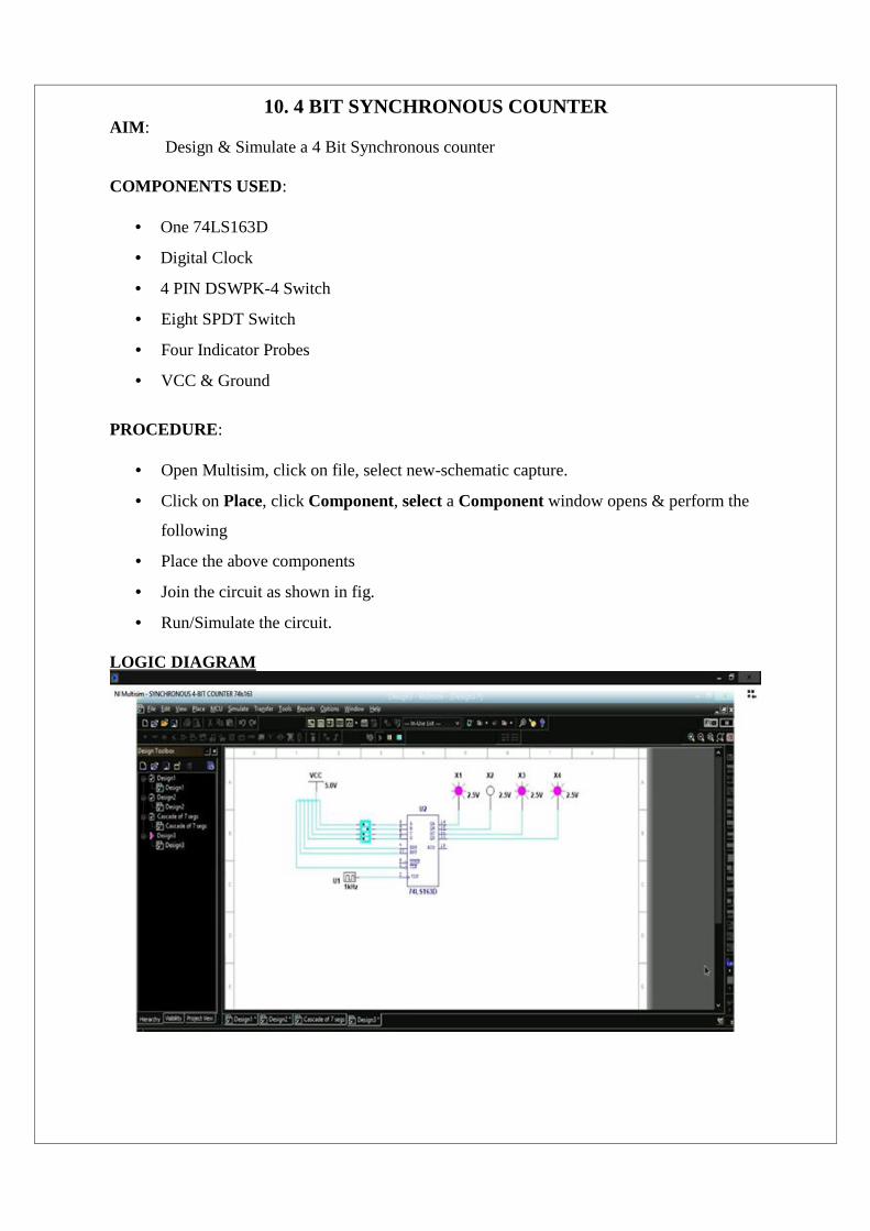
10. 4 BIT SYNCHRONOUS COUNTERAIM:
Design & Simulate a 4 Bit Synchronous counter
COMPONENTS USED:
One 74LS163D
Digital Clock
4 PIN DSWPK-4 Switch
Eight SPDT Switch
Four Indicator Probes
VCC & Ground
PROCEDURE:
Open Multisim, click on file, select new-schematic capture.
Click on Place, click Component, select a Component window opens & perform the
following
Place the above components
Join the circuit as shown in fig.
Run/Simulate the circuit.
LOGIC DIAGRAM
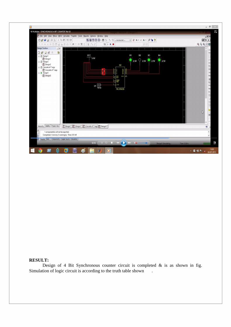
RESULT:Design of 4 Bit Synchronous counter circuit is completed & is as shown in fig.
Simulation of logic circuit is according to the truth table shown .

1. DESIGN OF ADDER & SUBTRACTORAIM:
Design & Simulate a Half adder circuit using matlab Simulink model
FUNCTIONS USED:
Constant Bit Function
Logical operators
Display system
PROCEDURE:
Open Matlab software, Click on file, click, select a model file, Simulink & perform the
following
Place the above components from commonly used blocks and SimElectronics tool box
Join the circuit as shown in fig.
Run/Simulate the circuit.
SIMULINK MODEL FOR HALF ADDER
RESULT:Design of Half adder circuit is completed & is as shown in fig. Simulation of logic circuit
is according to the truth table shown .

2. TESTING OF BASIC LOGIC GATESAIM:
Design & Simulate a Basic logic circuit using matlab Simulink model
FUNCTIONS USED:
Constant Bit Function
Logical operators
Display system
PROCEDURE:
Open Matlab software, Click on file, click, select a model file, Simulink & perform the
following
Place the above components from commonly used blocks and SimElectronics tool box
Join the circuit as shown in fig.
Run/Simulate the circuit.
SIMULINK MODEL FOR BASIC LOGIC GATES
RESULT:Design of Testing of Basic logic gates circuit is completed & is as shown in fig.
Simulation of logic circuit is according to the truth table shown

3. MASTER – SLAVE J K FLIP FLOP MODELINGAIM:
Design & Simulate a Master Slave JK Flip-flop circuit using matlab Simulink model
FUNCTIONS USED:
Constant Bit Function
M-S JK Flip flop block
Manual switch (SPDT)
Logical operators, Solver block, clock source,
Three Scope Display system
PROCEDURE:
Open Matlab software, Click on file, click, select a model file, Simulink & perform the
following
Place the above components from commonly used blocks and SimElectronics tool box
Join the circuit as shown in fig.
Run/Simulate the circuit.
SIMULINK MODEL FOR MASTER SLAVE JK FLIPFLOP
RESULT:Modeling of Master slave JK Flipflop circuit is completed & is as shown in fig.
Simulation of logic circuit is according to the truth table shown
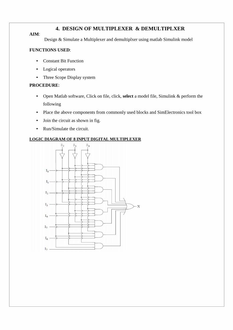
4. DESIGN OF MULTIPLEXER & DEMULTIPLXERAIM:
Design & Simulate a Multiplexer and demultiplxer using matlab Simulink model
FUNCTIONS USED:
Constant Bit Function
Logical operators
Three Scope Display system
PROCEDURE:
Open Matlab software, Click on file, click, select a model file, Simulink & perform the
following
Place the above components from commonly used blocks and SimElectronics tool box
Join the circuit as shown in fig.
Run/Simulate the circuit.
LOGIC DIAGRAM OF 8 INPUT DIGITAL MULTIPLEXER
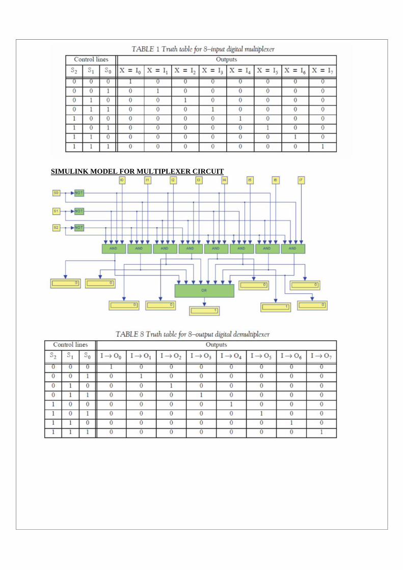
SIMULINK MODEL FOR MULTIPLEXER CIRCUIT
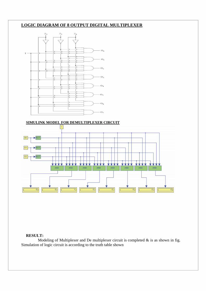
LOGIC DIAGRAM OF 8 OUTPUT DIGITAL MULTIPLEXER
SIMULINK MODEL FOR DEMULTIPLEXER CIRCUIT
RESULT:Modeling of Multiplexer and De multiplexer circuit is completed & is as shown in fig.
Simulation of logic circuit is according to the truth table shown
Related Documents