Science & Technology Facilities Council Rutherford Appleton Laboratory Development of Advanced MAPS for Scientific Applications Jamie Crooks CMOS Sensor Design Group Rutherford Appleton Laboratory UK 1 FEE Workshop 2009

Science & Technology Facilities Council Rutherford Appleton Laboratory Development of Advanced MAPS for Scientific Applications Jamie Crooks CMOS Sensor.
Dec 28, 2015
Welcome message from author
This document is posted to help you gain knowledge. Please leave a comment to let me know what you think about it! Share it to your friends and learn new things together.
Transcript

Science & Technology Facilities Council
Rutherford Appleton Laboratory
Development of Advanced MAPS for Scientific Applications
Jamie Crooks
CMOS Sensor Design Group
Rutherford Appleton Laboratory UK
1FEE Workshop 2009

Overview• Aim to give a summary of MAPS activity at RAL
• Technology– 4T pinned photodiode– Quadruple-well CMOS– High resistivity substrates– Stitching
• Example pixels– 4T pixel– 160T pixel
• Summary
2FEE Workshop 2009

CMOS Sensor Design Group at RAL
3FEE Workshop 2009
• Work on CMOS image sensors at RAL began in 1998
• The CMOS Sensor Design group was established in 2006
• Currently has eight members, led by Renato Turchetta
• The group designs CMOS image sensors for many applications including…• particle physics • space science• medical imaging • high-end commercial projects

MAPS requirements for Science• Low noise• High sensitivity• Radiation tolerance• Large pixels
– Often the <2um pixels from industry are not necessary
• Large sensing areas– Uninterrupted or
minimum “dead space”– Sparse readout– Region-of-Interest
readout
4FEE Workshop 2009
• Advanced pixel functionality– Pedestal correction– Analog preamplifiers– Thresholding– Event timing– ADC– Memories– Global shutter
Technology developments…

4T Pinned Photodiode• Pinning layer creates buried
diode• Transfer of charge to the
floating diffusion aided by electric field
• The diode is fully depleted following a transfer (ie “reset”)
FEE Workshop 2009 5
• Sensitivity (conversion gain) is set by the capacitance of the floating diffusion, not the diode• Can be optimised for target
application
• Architecture permits correlated double sampling • Low noise performance
Technology…

CMOS Imaging
FEE Workshop 2009 6
• MAPS pixels generally exclude PMOS transistors• Their N-well reduces
charge collection efficiency
• Applies to light / particles
• Regular imaging applications generally have no need for PMOS transistors in the pixel• Scientific applications
sometimes do
Technology…

Deep P-Well
FEE Workshop 2009 7
• We developed a “Deep P-Well” in collaboration with a leading CMOS image sensor foundry• High energy implant
creates a deep p-well• Selectively drawn
“under” n-wells in pixels• Change in doping
creates a potential barrier
• Diffusing charge is reflected back and not collected by the n-well
Technology…
Deep P-Well Implementation
• Device simulations– TCAD uses gds of pixels– Charge diffusion is modelled
• Layout– Drawn layer with design rules
• Manufacturing– MPW run is divided– some wafers receive DPW, others do not– Enables comparison of performance
FEE Workshop 2009 8

Substrate Resistivity
9FEE Workshop 2009
• Reference schematic• Pixel with deep p-well
• Depletion region illustrated – Standard resistivity
wafer– Diffusing charge that
reaches the depletion region is collected by electric field
Technology…

Substrate Resistivity
10FEE Workshop 2009
• Increased resistivity silicon enlarges the depletion region– Diffusing charge that
reaches the depletion region is collected by electric field
– Improved charge collection efficiency by larger catchment area
Technology…

Substrate Resistivity
11FEE Workshop 2009
• High resistivity (intrinsic) silicon enlarges the depletion region to fully occupy the pixel– Majority of deposited
charge now falls in a depletion region and is collected by electric field
– Improved charge collection efficiency
– Faster charge collection (drift vs diffusion)
Technology…

INMAPS Process• 0.18 micron commercial CMOS Imaging
Process• 4T pinned photodiodes• Choice of epitaxial layer thickness• Deep p-well• High resistivity substrates• Stitching• Multi-project runs for prototyping
– Option to vary starting material & implants per wafer
FEE Workshop 2009 12
9 multi-project submissions in last 2 years…
Technology…

Current Projects
FORTIS TPAC
FEE Workshop 2009 13
Examples…

Current Projects
FORTIS• Optical/Particle
applications• Explores 13 variants of a
4T pinned photodiode– Diode size– Pixel pitch– Pixel geometry
TPAC
FEE Workshop 2009 14
4T Test Image Sensor
4T Test Image Sensor
Examples…

4T Test Image Sensor
FEE Workshop 2009 15
• Development project– Design parameters
• Geometry
– Manufacturing parameters• DPW• Substrate material• Optimised implants
All pixels:

4T Pixel Characterisation• Photon Transfer Curve
– image-sensor standard test– Conversion gain = 61μV/e-
– Noise (equivalent) = 5.9e-
• 55Fe Photons (preliminary)– Conversion gain = 56 μ V/e-
– Noise (from dark fwhm) = 7.7e-
FEE Workshop 2009 16

4T Pixel Test Programme• Pixel characterisation
– PTC, Image Lag, 55Fe– Pixel design
• Pairs of pixel give direct comparison of key feature– Processing
• Optimal implants• Confirm DPW and 4T are compatible• Functional design on high-resistivity substrate• Charge collection efficiency
• Radiation tolerance (in progress)– Fully characterised sensors– 50KV x-ray tube– Incremental doses from 105 MRad– Repeat characterisation after irradiation
• Beam test– CERN beam test with EUDET pixel telescope in August– Evaluation of 4T architecture for particle physics applications
FEE Workshop 2009 17
100 different pixels to test!

Current Projects
FORTIS• Optical/Particle
applications• Explores 13 variants of a
4T pinned photodiode– Diode size– Pixel pitch– Pixel geometry
TPAC• Particle detection• Implements in-pixel circuits
– preAmplifier + shaper– comparator + logic– SRAM configuration memories
FEE Workshop 2009 18
Tera-Pixel Active Calorimeter
Tera-Pixel Active Calorimeter
Examples…

Tera-Pixel Active Calorimeter
SiW Digital ECAL for ILC• 30 layers silicon & tungsten• Demonstrate Monolithic Active Pixel Sensor
(MAPS) as a viable solution for the silicon
Sensor Specification• Sensitive to MIP signal• Small pixels determine “hit” status (binary
readout)• Store timestamp & location of “hits”• Target noise rate 10-6• Design to hold data for 8k bunch crossings • before readout• Minimum “dead space”
FEE Workshop 2009 19

TPAC Pixel
FEE Workshop 2009 20
• Gain 136uV/e• Noise 23e-• Power 8.9uW • 150ns “hit”
pulse wired to row logic
• Shaped pulses return to baseline
• 50um pixel• 4 diodes• 160 transistors• 27 unit capacitors• 1 resistor (4Mohm)• Configuration SRAM
• Per Pixel Mask• Comparator trim
(6 bits)

TPAC Pixel
FEE Workshop 2009 21
• Gain 136uV/e• Noise 23e-• Power 8.9uW • 150ns “hit”
pulse wired to row logic
• Shaped pulses return to baseline
• 50um pixel• 4 diodes• 160 transistors• 27 unit capacitors• 1 resistor (4Mohm)• Configuration SRAM
• Per Pixel Mask• Comparator trim
(6 bits)
DPWNW
M1PO

TPAC Architecture
FEE Workshop 2009 22
• 8.2 million transistors• 28224 pixels; 50 microns; 4 variants• Sensitive area 79.4mm2
– of which 11.1% “dead” (logic)
• Four columns of logic + SRAM– Logic columns serve 42 pixels– Record hit locations &
timestamps– Local SRAM
• Data readout– Slow (<5Mhz)– Current sense amplifiers– Column multiplex– 30 bit parallel data output

TPAC Test Programme• TPAC1.0 Test pixels
– Charge collection profile (laser)• Compare with device simulation
• TPAC1.0 Array pixels– Two variants of the pre-shaper pixel– Pedestal variation trim
adjustment– Gain uniformity
• TPAC1.1 Test pixels– Charge collection profile (laser)– Gain & noise calibration (55Fe)
• TPAC1.1 Array pixels– Capacitive coupling problem
FEE Workshop 2009 23
1.0
1.1
4 pixel variants in arrayTwo “sampler” test pixelsDifferent epi thicknessesWith/without DPW
1 pixel variant in arrayTwo “shaper” test pixelsUpgraded 4 6 trim bitsImproved matching of RWith/without DPWStandard & Hi-Res Substrates
Shielding added in pixel1.2

Charge collection efficiency
FEE Workshop 2009 24
• 2x2μm focussed IR laser spot• 1064nm laser• The laser is raster-scanned
over an 200x200 area• The test pixel is surrounded by
dummy neighbours• Signal magnitude (mV) is
plotted in the z (colour) axis for each position of the laser spot
– Averaged (50 samples)
• The overlaid pixel structure shows n-wells (solid line) and deep p-well (dotted line)

Measured vs Simulation Results
FEE Workshop 2009 25
• Amplitude results• With/without deep pwell• Qualitative comparison
• Simulations “GDS”• Measurements “Real”
F
B
Pixel profiles

Charge collection (diffusion) time
26
17μm
Timing measuremen
t(30mV threshold)
TCADSimulation
(Q=90%)
Measured timing includes a fixed laser-fire delay
BC
M

Gain Calibration with 55Fe• 55Fe photons will deposit 1620e- at random locations in the
pixel volume– The deposited charge will diffuse and be collected at several
diodes
• A tiny fraction of these deposits will be within the depletion region of a single diode– The full 1620e- will be collected– This gives an absolute calibration of gain– The histogram of recorded signals will show a peak for 1620e-
• Secondary peak at 1778e-
FEE Workshop 2009 27
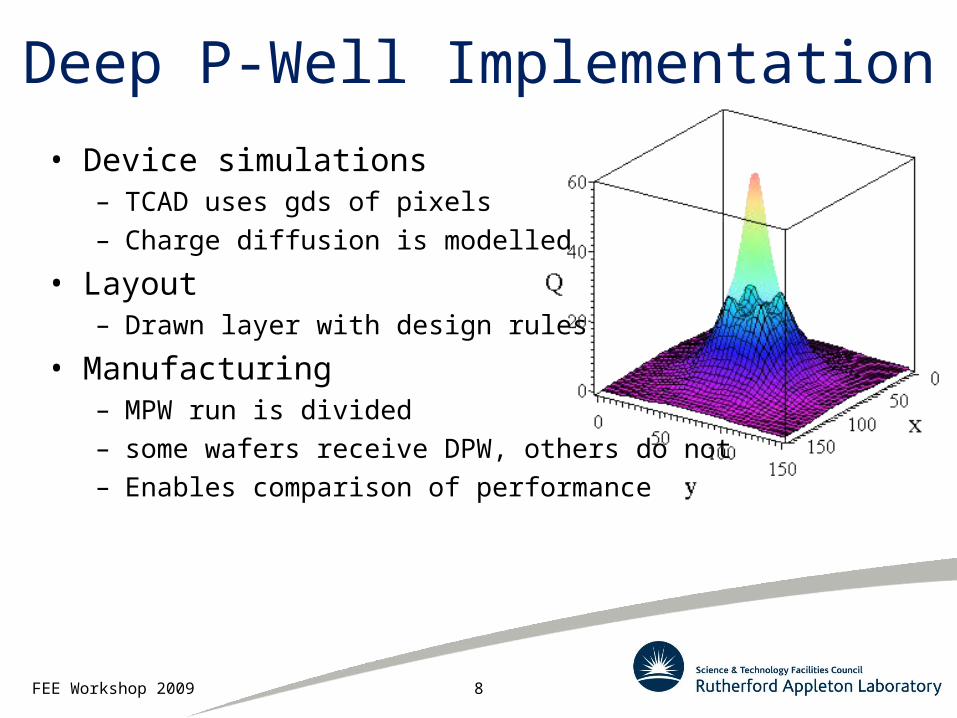
Histogram of 55Fe Events
FEE Workshop 2009 28
Low “threshold” on oscilloscopeInvestigates full distribution of
hits
High “threshold” on oscilloscope
Investigates 55Fe peak
• Kα peak fit• Kβ peak fit
• With deep p-well• Without deep p-well
• Primary 55Fe peak gives calibrated gain of 128µV/e-• Width of 55Fe peak gives noise of 27e-

Histogram of 55Fe Events
FEE Workshop 2009 29
?
• With deep p-well• Without deep p-well
• Why the peak at ~30% signal? • Basic diffusion model
– Deposit 55Fe at different heights– Shows ~30% as a probable value
• Deep p-well prevents many deposits in pixel centre being collected
• They diffuse and tend to read as ~30%
With DPWWithout DPW

TPAC Pixel Arrays• Per-pixel noise
– Meas. by threshold scan– Generate trim settings &
load
FEE Workshop 2009 30
• Pixel gain uniformity– Laser stimulus
• Hit each pixel in turn• Threshold scan
– 55Fe photons• Threshold scan• Use peak
12%
13%

TPAC Test Programme• TPAC1.0 Test pixels
– Charge collection profile (laser)• Compare with device simulation
• TPAC1.0 Array pixels– Two variants of the pre-shaper pixel– Pedestal variation trim
adjustment– Gain uniformity
• TPAC1.1 Test pixels– Charge collection profile (laser)– Gain & noise calibration (55Fe)
FEE Workshop 2009 31
4 layerstack
• TPAC1.2 Test pixels– Charge collection
characteristics on high resistivity substrate
• TPAC1.2 Array pixels– Pixel uniformity– Noise performance– Crosstalk/pickup– Cosmics – Beam test

Stitching
• 56mm sensor– 22mm variant– 11mm variant
FEE Workshop 2009 32
• 61mm sensor
Allows a seamless pixel array up to 130x130mm on a 200mm wafer
Same mask set can make different size sensors

Science & Technology Facilities Council
Rutherford Appleton Laboratory
MAPS Activity at RAL
• Our recent technology developments have achieved– 4T pinned photodiode sensor <6e- noise– Sensors with deep P-Well shown to preserve charge
collection with full CMOS in a pixel– Two MAPS designs manufactured on Hi-Resistivity– Two stitched MAPS designs
FEE Workshop 2009 33

Science & Technology Facilities Council
Rutherford Appleton Laboratory
Acknowledgements/Collaborators
FEE Workshop 2009 34
SPiDeR

Science & Technology Facilities Council
Rutherford Appleton Laboratory
Spare slides
• Stitching “animations”
FEE Workshop 2009 35

Stitching 1• Optical reticle
divided into 4 main areas for each chip
• Sensor is constructed by repeating the blocks N times to create larger device
A
BD
C

AA
BD
CC‘Stitching’
BD
A A
A A A
A A A
B B
B B B
C
C
C
C
C
D
D D
Top sections contain pixel reset control circuits
Bottom sections contain column addressing and analogue readout circuits 2 Outputs per section
Left Edge contains row addressing and reset control circuits
Stitching 2

Stitching 3
Related Documents