YFP PACKAGE (TOP VIEW) D E A 1 2 3 4 B C TXS0206-29 www.ti.com SCES690 – DECEMBER 2009 MMC, SD CARD, Memory Stick™ VOLTAGE-TRANSLATION TRANSCEIVER AND LDO VOLTAGE REGULATOR WITH ESD PROTECTION AND EMI FILTERING 1FEATURES • Level Translator • ESD Protection Exceeds JESD 22 (A Port) – V CCA Range of 1.1 V to 3.6 V – 2000-V Human-Body Model (A114-B) – Fast Propagation Delay (4 ns Max When – 1000-V Charged-Device Model (C101) Translating Between 1.8 V and 2.9 V) • ±8-kV Contact Discharge IEC 61000-4-2 ESD • Low-Dropout (LDO) Regulator (B Port) – 200-mA LDO Regulator With Enable – 2.9-V Output Voltage – 3.05-V to 5.5-V Input Voltage Range – Very Low Dropout: 200 mV at 200 mA TERMINAL ASSIGNMENTS 1 2 3 4 A DAT2A V CCA WP/CD DAT2B B DAT3A V BATT V CCB O/P DAT3B C CMDA GND GND CMDB D DAT0A CLKA CLKB DAT0B E DAT1A CLK-f EN DAT1B DESCRIPTION/ORDERING INFORMATION The TXS0206-29 is a complete solution for interfacing microprocessors with MultiMediaCards (MMCs), secure digital (SD) cards, and Memory Stick™ cards. It is comprised of a high-speed level translator, a low-dropout (LDO) voltage regulator, IEC level ESD protection, and EMI filtering circuitry. The voltage-level translator has two supply voltage pins. V CCA can be operated over the full range of 1.1 V to 3.6 V. V CCB is set at 2.9 V and is supplied by an internal LDO. The integrated LDO accepts input voltages from 3.05V to as high as 5.5 V and outputs 2.9 V, 200 mA to the B-side circuitry and to the external memory card. The TXS0206-29 enables system designers to easily interface low-voltage microprocessors to memory cards operating at 2.9 V. Memory card standards recommend high-ESD protection for devices that connect directly to the external memory card. To meet this need, the TXS0206-29 incorporates ±8-kV Contact Discharge protection on the card side. Since memory cards are widely used in mobile phones, PDAs, digital cameras, personal media players, camcorders, set-top boxes, etc. Low static power consumption and small package size make the TXS0206-29 an ideal choice for these applications. The TXS0206-29 is offered in a 20-bump wafer chip scale package (WCSP). This package has dimensions of 1.96 mm × 1.56 mm, with a 0.4-mm ball pitch for effective board-space savings ORDERING INFORMATION (1) T A PACKAGE (2) ORDERABLE PART NUMBER TOP-SIDE MARKING (3) –40°C to 85°C WCSP – YFP (Pb-free) Tape and reel TXS0206-29YFPR ___3V2 (1) For the most current package and ordering information, see the Package Option Addendum at the end of this document, or see the TI web site at www.ti.com. (2) Package drawings, thermal data, and symbolization are available at www.ti.com/packaging. (3) The actual top-side marking has three preceding characters to denote year, month, and sequence code. 1 Please be aware that an important notice concerning availability, standard warranty, and use in critical applications of Texas Instruments semiconductor products and disclaimers thereto appears at the end of this data sheet. PRODUCTION DATA information is current as of publication date. Copyright © 2009, Texas Instruments Incorporated Products conform to specifications per the terms of the Texas Instruments standard warranty. Production processing does not necessarily include testing of all parameters.

Welcome message from author
This document is posted to help you gain knowledge. Please leave a comment to let me know what you think about it! Share it to your friends and learn new things together.
Transcript

YFP PACKAGE(TOP VIEW)
D
E
A
1 2 3 4
B
C
TXS0206-29
www.ti.com SCES690 –DECEMBER 2009
MMC, SD CARD, Memory Stick™ VOLTAGE-TRANSLATION TRANSCEIVER AND LDOVOLTAGE REGULATOR WITH ESD PROTECTION AND EMI FILTERING
1FEATURES• Level Translator • ESD Protection Exceeds JESD 22 (A Port)
– VCCA Range of 1.1 V to 3.6 V – 2000-V Human-Body Model (A114-B)– Fast Propagation Delay (4 ns Max When – 1000-V Charged-Device Model (C101)
Translating Between 1.8 V and 2.9 V) • ±8-kV Contact Discharge IEC 61000-4-2 ESD• Low-Dropout (LDO) Regulator (B Port)
– 200-mA LDO Regulator With Enable– 2.9-V Output Voltage– 3.05-V to 5.5-V Input Voltage Range– Very Low Dropout: 200 mV at 200 mA
TERMINAL ASSIGNMENTS1 2 3 4
A DAT2A VCCA WP/CD DAT2B
B DAT3A VBATT VCCB O/P DAT3B
C CMDA GND GND CMDB
D DAT0A CLKA CLKB DAT0B
E DAT1A CLK-f EN DAT1B
DESCRIPTION/ORDERING INFORMATIONThe TXS0206-29 is a complete solution for interfacing microprocessors with MultiMediaCards (MMCs), securedigital (SD) cards, and Memory Stick™ cards. It is comprised of a high-speed level translator, a low-dropout(LDO) voltage regulator, IEC level ESD protection, and EMI filtering circuitry.
The voltage-level translator has two supply voltage pins. VCCA can be operated over the full range of 1.1 V to3.6 V. VCCB is set at 2.9 V and is supplied by an internal LDO. The integrated LDO accepts input voltages from3.05V to as high as 5.5 V and outputs 2.9 V, 200 mA to the B-side circuitry and to the external memory card. TheTXS0206-29 enables system designers to easily interface low-voltage microprocessors to memory cardsoperating at 2.9 V.
Memory card standards recommend high-ESD protection for devices that connect directly to the external memorycard. To meet this need, the TXS0206-29 incorporates ±8-kV Contact Discharge protection on the card side.
Since memory cards are widely used in mobile phones, PDAs, digital cameras, personal media players,camcorders, set-top boxes, etc. Low static power consumption and small package size make the TXS0206-29 anideal choice for these applications. The TXS0206-29 is offered in a 20-bump wafer chip scale package (WCSP).This package has dimensions of 1.96 mm × 1.56 mm, with a 0.4-mm ball pitch for effective board-space savings
ORDERING INFORMATION (1)
TA PACKAGE (2) ORDERABLE PART NUMBER TOP-SIDE MARKING (3)
–40°C to 85°C WCSP – YFP (Pb-free) Tape and reel TXS0206-29YFPR _ _ _ 3 V 2
(1) For the most current package and ordering information, see the Package Option Addendum at the end of this document, or see the TIweb site at www.ti.com.
(2) Package drawings, thermal data, and symbolization are available at www.ti.com/packaging.(3) The actual top-side marking has three preceding characters to denote year, month, and sequence code.
1
Please be aware that an important notice concerning availability, standard warranty, and use in critical applications of TexasInstruments semiconductor products and disclaimers thereto appears at the end of this data sheet.
PRODUCTION DATA information is current as of publication date. Copyright © 2009, Texas Instruments IncorporatedProducts conform to specifications per the terms of the TexasInstruments standard warranty. Production processing does notnecessarily include testing of all parameters.

E4
A4
B4
D4
DAT1B
DAT2B
DAT3B
WP
DAT0B
DAT1B
CLKB
CMDB
CLKB
DAT0B
0
1
2
3
4
5
6
7
8
9
10
11
12
13
VCCA
DAT0A
DAT1A
DAT2A
DAT3A
CMDA
CLKA
CLK-f
GND
GND
VCCB O/P
DAT0B
DAT1B
DAT2B
DAT3B
CMDB
CLKB
VDDA
DAT0
DAT1
DAT2
DAT3
CMD
CLK
CLKin
GND
WP/CD
DAT2
DAT3
CMD
VSS1
VDD
CLK
VSS2
DAT0
DAT1
WP/CD (Physical)
CD (Physical)
GND
GND
WP (Physical)
A2
D1
E1
A1
B1
C1
D2
E2
C2
C3
VCCA VCCB
Processor
SD/SDIO MMCTXS0206-29
C3
0.1 μF
C4
0.1 μF
C1
0.1 μF
VCCB
U1A U2 J1
DAT2B
DAT3B
CMDB
B3
C4
D3CD
WP/CD
WP/CDA3
54794-0978
SD/SDIO
CardConnector
Level-ShifterIntegrated
ASIPEMI Filter
Integrated Pullup/Pulldown Resistors
Integrated PSU2.9 V, 200 mA
Feedback CLK
CLK
A Side1.8 V 2.9 VB Side
CLK
CMD
CMD
Data 0–3
Data 0–3
EN
WP, CD
WP, CD
AntennaPins 10, 11
WP, CD 1.8-V Pullup
ESD – ±8-kV Contact DischargeESD – 2 kV
MMC,SD Card, or
MS Card
CPU
TXS0206-29
SCES690 –DECEMBER 2009 www.ti.com
REFERENCE DESIGN
Figure 1. Interfacing With SD/SDIO Card
Figure 2. Typical Application Circuit
2 Submit Documentation Feedback Copyright © 2009, Texas Instruments Incorporated

TXS0206-29
www.ti.com SCES690 –DECEMBER 2009
Table 1. LOGIC TABLE
EN LDO TRANSLATOR I/Os
Disabled, pulled to VCCA, VCCB O/P through R1 and R2L Disabled at 70kΩ pullup resistors respectively
H Active Active
TERMINAL FUNCTIONSTERMINAL
TYPE DESCRIPTIONNO. NAME
A1 DAT2A I/O Data bit 2 connected to host. Referenced to VCCA. Includes R1 pullup resistor to VCCA (see Note A).
A2 VCCA Power A-port supply voltage. VCCA powers all A-port I/Os and control inputs.
Connected to write protect on the mechanical connector. The WP pin has an internal 100-kΩ pullupA3 WP/CD Output resistor to VCCA.
Data bit 2 connected to memory card. Referenced to VCCBO/P. Includes R2 pullup resistor toA4 DAT2B I/O VCCBO/P (see Note A).
B1 DAT3A I/O Data bit 3 connected to host. Referenced to VCCA . Includes R1 pullup resistor to VCCA (see Note A).
B2 VBATT Input LDO input voltage from Battery-Supply
B3 VCCB O/P Output LDO output voltage and B-port supply voltage. VCCBO/P powers all B-port I/Os.
Data bit 3 connected to memory card. Referenced to VCCBO/P. Includes R2 pullup resistor toB4 DAT3B I/O VCCBO/P (see Note A).
Command bit connected to host. Referenced to VCCA . Includes R1 pullup resistor to VCCA (see NoteC1 CMDA I/O A).
C2, GND GroundC3
Command bit connected to memory card. Referenced to VCCBO/P. Includes R2 pullup resistor toC4 CMDB I/O VCCBO/P (see Note A).
D1 DAT0A I/O Data bit 0 connected to host. Referenced to VCCA . Includes R1 pullup resistor to VCCA (see Note A).
D2 CLKA Input Clock signal connected to host. Referenced to VCCA.
D3 CLKB Output Clock signal connected to memory card. Referenced to VCCBO/P.
Data bit 0 connected to memory card. Referenced to VCCBO/P. Includes R2 pullup resistor toD4 DAT0B I/O VCCBO/P (see Note A).
E1 DAT1A I/O Data bit 1 connected to host. Referenced to VCCA . Includes R1 pullup resistor to VCCA (see Note A).
E2 CLK-f Output Clock feedback to host for resynchronizing data to a processor. Leave unconnected if not used.
Enable/disable control. Pull EN low to place all outputs in Hi-Z state and to disable the LDO.E3 EN Input Referenced to VCCA.
Data bit 1 connected to memory card. Referenced to VCCBO/P. Includes R2 pullup resistor toE4 DAT1B I/O VCCBO/P (see Note A).
Copyright © 2009, Texas Instruments Incorporated Submit Documentation Feedback 3
VCCA VCCB
Translator
One-Shot
One-Shot
CMDB
R2
(see Note A)
Gate ControlCMDA
R1
(see Note A)
Translator
One-Shot
One-Shot
CLKA
CLKB
CLK-f
EN
(see Note B)
VCCA VCCB
Translator
One-Shot
One-Shot
DAT0B
R2
(see Note A)
Gate ControlDAT0A
R1
(see Note A)
Translator
One-Shot
One-Shot
VCCA VCCB
Translator
One-Shot
One-Shot
DAT1B
R2
(see Note A)
Gate ControlDAT1A
R1
(see Note A)
Translator
One-Shot
One-Shot
VCCA VCCB
Translator
One-Shot
One-Shot
DAT2B
R2
(see Note A)
Gate ControlDAT2A
R1
(see Note A)
Translator
One-Shot
One-Shot
VCCA VCCB
Translator
One-Shot
One-Shot
DAT3B
R2
(see Note A)
Gate ControlDAT3A
R1
(see Note A)
Translator
One-Shot
One-Shot
WP/CD
100 kW
VCCA VCCB
VCCA
TXS0206-29
SCES690 –DECEMBER 2009 www.ti.com
A. R1 and R2 resistor values are determined based upon the logic level applied to the A port or B port as follows:R1 and R2 = 40 kΩ when a logic level low is applied to the A port or B port.R1 and R2 = 4 kΩ when a logic level high is applied to the A port or B port.R1 and R2 = 70 kΩ when the port is deselected (or in High-Z or 3-state).
B. EN controls all output buffers. When EN = low, all outputs are Hi-Z.
Figure 3. Logic Diagram
4 Submit Documentation Feedback Copyright © 2009, Texas Instruments Incorporated
40 Ω
40 kΩ
R1, R2, R3, R4, R5, R6
R7, R8, R9, R10, R11
±20%
±30%
Tolerance
Data3
Data2
Data1
Data0
CMD
CLK
R1
R7
R2
R4
R6
GND
R3
R5
HOST
VCCB
DAT2B
DAT3B
DAT1B
DAT0B
CMDB
CLKB
CARD
Tolerance
RESISTORS
14 V at 1 mAVbr min
<20 pFLine capacitance
BIDIRECTIONAL ZENER DIODES
R8 R9 R10 R11
GND
RESISTORS
RWP/CD
Tolerance
100 kΩ
±30%
VCCA
RWP/CD
WP/CD
TXS0206-29
www.ti.com SCES690 –DECEMBER 2009
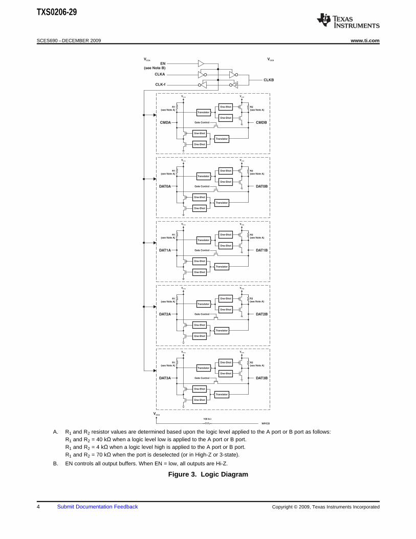
Figure 4. ASIP Block Diagram
Figure 5. WP/CD Pullup Resistor
Copyright © 2009, Texas Instruments Incorporated Submit Documentation Feedback 5
TXS0206-29
SCES690 –DECEMBER 2009 www.ti.com
ABSOLUTE MAXIMUM RATINGS (1)
Level Translatorover operating free-air temperature range (unless otherwise noted)
MIN MAX UNIT
VCCA Supply voltage range –0.5 4.6 V
I/O ports (A port) –0.5 4.6
VI Input voltage range I/O ports (B port) –0.5 4.6 V
Control inputs –0.5 4.6
A port –0.5 4.6Voltage range applied to any output in the high-impedance orVO Vpower-off state B port –0.5 4.6
A port –0.5 4.6VO Voltage range applied to any output in the high or low state V
B port –0.5 4.6
IIK Input clamp current VI < 0 –50 mA
IOK Output clamp current VO < 0 –50 mA
IO Continuous output current ±50 mA
Continuous current through VCCA or GND ±100 mA
Tstg Storage temperature range –65 150 °C
(1) Stresses beyond those listed under "absolute maximum ratings" may cause permanent damage to the device. These are stress ratingsonly, and functional operation of the device at these or any other conditions beyond those indicated under "recommended operatingconditions" is not implied. Exposure to absolute-maximum-rated conditions for extended periods may affect device reliability.
THERMAL IMPEDANCE RATINGSTYP UNIT
θJA Package thermal impedance (1) 117 °C/W
(1) The package thermal impedance is calculated in accordance with JESD 51-7.
ABSOLUTE MAXIMUM RATINGS (1)
LDOover operating free-air temperature range (unless otherwise noted)
MIN MAX UNIT
VIN Input voltage range 2.3 6.5 V
VOUT Output voltage range –0.3 4.6 V
Peak output current 220 mA
Continuous total power dissipation TBD mW
TJ Junction temperature range –55 150 °C
Tstg Storage temperature range –55 150 °C
(1) Stresses beyond those listed under "absolute maximum ratings" may cause permanent damage to the device. These are stress ratingsonly, and functional operation of the device at these or any other conditions beyond those indicated under "recommended operatingconditions" is not implied. Exposure to absolute-maximum-rated conditions for extended periods may affect device reliability.
6 Submit Documentation Feedback Copyright © 2009, Texas Instruments Incorporated

TXS0206-29
www.ti.com SCES690 –DECEMBER 2009
RECOMMENDED OPERATING CONDITIONS (1)
Level TranslatorVCCA VCCB MIN MAX UNIT
VCCA Supply voltage 1.1 3.6 V
1.1 V to 1.95 V VCCI – 0.2 VCCIA-Port CMD and 2.9 VDATA I/Os 1.95 V to 3.6 V VCCI – 0.4 VCCI
VIH High-level input voltage 1.1 V to 1.95 V VCCI – 0.2 VCCI VB-Port and DATAI/Os 1.95 V to 3.6 V 2.9 V VCCI – 0.4 VCCI
OE and CLKA 1.1 V to 3.6 V VCCI × 0.65 VCCI
1.1 V to 1.95 V 0 0.15A-Port CMD and 2.9 VDATA I/Os 1.95 V to 3.6 V 0 0.15
VIL Low-level input voltage 1.1 V to 1.95 V 0 0.15 VB-Port CMD andDATA I/Os 1.95 V to 3.6 V 2.9 V 0 0.15
OE and CLKA 1.1 V to 3.6 V 0 VCCI × 0.35
Active stateVO Output voltage 0 VCCO V
3-state
1.1 V to 1.3 V –0.5
1.4 V to 1.6 V –1
IOH High-level output current (CLK-f output) 1.65 V to 1.95 V 2.9 V –2 mA
2.3 V to 2.7 V –4
3 V to 3.6 V –8
1.1 V to 1.3 V 0.5
1.4 V to 1.6 V 1
IOL Low-level output current (CLK-f output) 1.65 V to 1.95 V 2.9 V 2 mA
2.3 V to 2.7 V 4
3 V to 3.6 V 8
IOH High-level output current (CLK output) 2.9 V –8 mA
IOL Low-level output current (CLK output) 2.9 V 8 mA
Δt/Δv Input transition rise or fall rate 5 ns/V
TA Operating free-air temperature –40 85 °C
(1) All unused data inputs of the device must be held at VCCI or GND to ensure proper device operation. See the TI application report,Implications of Slow or Floating CMOS Inputs, literature number SCBA004.
RECOMMENDED OPERATING CONDITIONSLDO
MIN MAX UNIT
IOUT(PK) Peak output current 200 mA
COUT Output capacitance 1 100 μF
TJ Operating junction temperature –40 125 °C
Copyright © 2009, Texas Instruments Incorporated Submit Documentation Feedback 7

TXS0206-29
SCES690 –DECEMBER 2009 www.ti.com
ELECTRICAL CHARACTERISTICSLevel Translatorover recommended operating free-air temperature range (unless otherwise noted)
PARAMETER TEST CONDITIONS VCCA VCCBO/P MIN TYP (1) MAX UNIT
IOH = –100 μA 1.1 V to 3.6 V VCCA × 0.8
IOH = –0.5 mA 1.1 V 0.8
IOH = –1 mA 1.4 V 1.05A port(CLK-f output) IOH = –2 mA 1.65 V 1.2
VOH 2.9 V VIOH = –4 mA 2.3 V 1.75
IOH = –8 mA 3 V 2.3
A port(DAT and CMD IOH = –20 μA 1.1 V to 3.6 V VCCA × 0.8outputs)
IOL = 100 μA 1.1 V to 3.6 V VCCA × 0.8
IOL = 0.5 mA 1.1 V 0.35
IOL = 1 mA 1.4 V 0.35A port 2.9 V V(CLK-f output) IOL = 2 mA 1.65 V 0.45
IOL = 4 mA 2.3 V 0.55
VOL IOL = 8 mA 3 V 0.7
IOL = 135 μA 0.4
IOL = 180 μA 0.4A port(DAT and CMD IOL = 220 μA 1.1 V to 3.6 V 2.9 V 0.4 Voutputs) IOL = 300 μA 0.4
IOL = 400 μA 0.55
VCCBO/P ×IOH = –100 μAB port 0.82.9 V(CLK output)VOH IOH = –8 mA 1.1 V to 3.6 V 2.3 V
B port VCCBO/P ×IOH = –20 μA 2.9 V(DAT output) 0.8
VCCBO/P ×IOL = 100 μACLKB output 0.81.1 V to 3.6 V 2.9 V VportIOL = 8 mA 0.7
IOL = 135 μA 0.4VOL IOL = 180 μA 0.4B port
(DAT and CMD IOL = 220 μA 1.1 V to 3.6 V 2.9 V 0.4 Voutputs) IOL = 300 μA 0.4
IOL = 400 μA 0.55
II Control inputs VI = VCCA or GND 1.1 V to 3.6 V 2.9 V ±1 μA
ICCA VI = VCCI or GND, IO = 0 1.1 V to 3.6 V 2.9 V 6 μA
ICCB VI = VCCI or GND, IO = 0 1.1 V to 3.6 V 2.9 V 5 μA
A port 5.5 6.5Cio pF
B port 15 17.5
Control inputs 3.5 4.5Ci VI = VCCA or GND pF
Clock input 3 4
(1) All typical values are at TA = 25°C.
8 Submit Documentation Feedback Copyright © 2009, Texas Instruments Incorporated

TXS0206-29
www.ti.com SCES690 –DECEMBER 2009
ELECTRICAL CHARACTERISTICSLDOover operating free-air temperature range (unless otherwise noted)
PARAMETER TEST CONDITIONS MIN TYP (1) MAX UNIT
VBATT Input voltage VOUT + VDO 5.5 V
Nominal TA = 25°C 2.9VOUT Output voltage V
All conditions 2.75 3.05
ΔVOUT Output voltage tolerance Nominal TA = 25°C ±3 %
VDO Dropout voltage IOUT = 200 mA 200 250 mV
IOUT = 0 40
IGND Ground-pin current IOUT < 100 mA 200 μA
100 mA ≤ IOUT ≤ 200 mA 400
IOUT(SC) Short-circuit current RL = 0 Ω 300 mA
f = 1 kHz 50VIN = 3.05 V, VOUT = 2.9 V,PSRR Power-supply rejection ratio dBCNR = 0.01 μF, IOUT = 200 mA f = 10 kHz 40
tSTR Start-up time VOUT = 2.9 V, IOUT = 200 mA, COUT = 2.2 μF 200 μs
(1) All typical values are at TA = 25°C.
TIMING REQUIREMENTSover recommended operating free-air temperature range, VCCB = 2.9 V ± 5% (unless otherwise noted)
VCCA = 1.2 V VCCA = 1.5 V VCCA = 1.8 V VCCA = 2.5 V VCCA = 3.3 V± 0.1 V ± 0.1 V ± 0.15 V ± 0.2 V ± 0.3 V UNIT
MIN MAX MIN MAX MIN MAX MIN MAX MIN MAX
Push-pull driving 40 60 60 60 60Command Mbps
Open-drain driving 1 1 1 1 1Data rate
Clock 60 60 60 60 60 MHzPush-pull driving
Data 40 60 60 60 60 Mbps
Push-pull driving 25 17 17 17 17 nsCommand
Open-drain driving 1 1 1 1 1 μsPulsetW duration Clock 8.3 8.3 8.3 8.3 8.3 nsPush-pull driving
Data 25 17 17 17 17 ns
Copyright © 2009, Texas Instruments Incorporated Submit Documentation Feedback 9

TXS0206-29
SCES690 –DECEMBER 2009 www.ti.com
SWITCHING CHARACTERISTICSover recommended operating free-air temperature range, VCCB = 2.9 V ± 5% (unless otherwise noted)
VCCA VCCA VCCA VCCA VCCA= 1.2 V = 1.5 V = 1.8 V = 2.5 V = 3.3 VFROM TO TESTPARAMETER UNIT± 0.1 V ± 0.1 V ± 0.15 V ± 0.2 V ± 0.3 V(INPUT) (OUTPUT) CONDITIONS
MIN MAX MIN MAX MIN MAX MIN MAX MIN MAX
Push-pull driving 10.8 6.1 4.6 3.7 3.8
Open-drain driving 3.2 10.6 2.7 6.6 2.4 5.5 2.1 4.4 2 4.1CMDA CMDB (H-to-L)
Open-drain driving 71 175 83 180 89 201 98 249 101 233(L-to-H)
Push-pull driving 12 6.8 5.2 4.1 3.4
Open-drain driving 2.9 9.4 2.1 7.3 2 6.4 2 5.7 2.2 4.6tpd nsCMDB CMDA (H-to-L)
Open-drain driving 77 243 87 214 93 215 99 261 105 248(L-to-H)
CLKA CLKB Push-pull driving 11.7 6.2 4.7 3.7 3.5
DATxA DATxB 11.1 6.2 4.7 3.7 3.7Push-pull driving
DATxB DATxA 11.5 6.2 5 3.9 6.2
CLKA CLK-f Push-pull driving 24.7 13 8.9 6.8 4.8
EN B-port Push-pull driving 1 1 1 1 1ten μs
EN A-port Push-pull driving 1 1 1 1 1
EN B-port Push-pull driving 40 39 35 38 34tdis ns
EN A-port Push-pull driving 40 38 38 38 36
Push-pull driving 1.6 12.2 0.4 8.3 1.1 5.9 1.9 3.3 0.8 4.2CMDA rise time
Open-drain driving 32 120 44 127 52 150 62 201 74 194trA ns
CLK-f rise time 0.6 12.7 0.5 7.2 0.4 4.5 0.7 1.5 0.7 1.4Push-pull driving
DATxA rise time 1.6 11.6 0.6 8.4 1 6.3 1.8 4.2 1.1 3.3
Push-pull driving 1.7 6.7 0.5 5.6 1 5.2 1.5 5.2 1.9 5CMDB rise time
Open-drain driving 66 214 71 196 73 184 76 214 79 185trB ns
CLKB rise time 1.7 4.8 1.5 4.9 1.5 4.9 1.6 5 1.6 5.1Push-pull driving
DATxB rise time 0.4 6.8 0.6 5 0.2 5.2 0.9 5.3 1 14
Push-pull driving 0.8 4 0.8 2.3 0.2 3.1 0.3 1.5 1 2.3CMDA fall time
Open-drain driving 1.6 3.9 1.6 3.7 1.6 3.7 1.6 3.7 1.6 3.9tfA ns
CLK-f fall time 1 4 0.4 6.8 0.1 1.5 0.3 2.8 0.6 1.3Push-pull driving
DATxA fall time 1 3.9 0.1 3.8 0.2 2.7 0.3 2.9 0.4 1.8
Push-pull driving 1.5 4.5 1.4 5.4 1.6 5 1.6 5.6 0.8 6.3CMDB fall time
Open-drain driving 1 4.3 1 2.3 0.8 1.9 0.8 1.6 0.9 1.3tfB ns
CLKB fall time 1.6 4 1.6 4.1 1.7 4.2 1.7 4.5 0.9 5.1Push-pull driving
DATxB fall time 1 4.8 2.3 4.3 0.8 4.9 0.2 4.9 0.8 6.9
Channel-to-channeltSK(O) Push-pull driving 1 1 1 1 1 nsskew
Push-pull driving 40 60 60 60 60Command Mbps
Open-drain driving 1 1 1 1 1Max data rate
Clock 60 60 60 60 60 MHzPush-pull driving
Data 40 60 60 60 60 Mbps
10 Submit Documentation Feedback Copyright © 2009, Texas Instruments Incorporated

TXS0206-29
www.ti.com SCES690 –DECEMBER 2009
OPERATING CHARACTERISTICSTA = 25°C, VCCB = 2.9 V
VCCA TYPTESTPARAMETER UNITCONDITIONS 1.2 V 1.5 V 1.8 V 2.5 V 3 V 3.3 V
CLK 15 15 15 15.7 17.1 17.1A-port input, EnabledB-port
DATAoutput 6.3 6.4 6.5 6.5 6.5 6.5Enabled
B-port input, DATAA-port 12.5 12.3 12.3 12.5 14 14Enabled CL = 0,outputCpdA
(1) f = 10 MHz, pFCLK tr = tf = 1 ns 0.2 0.2 0.2 0.3 0.3 0.3A-port input, Disabled
B-portDATAoutput 1.2 1.2 1.2 1.2 1.2 1.2Disabled
B-port input, DATAA-port 0.2 0.2 0.2 0.3 0.3 0.3Disabledoutput
A-port input, DATAB-port 31.2 30.6 30.3 29.5 28.5 28.5Enabledoutput
CLK 28.1 27.2 27 26.9 27 27B-port input, EnabledA-port
DATAoutput 12.9 12.8 12.9 13.2 13.2 13.2CL = 0,EnabledCpdB
(1) f = 10 MHz, pFA-port input, tr = tf = 1 nsDATAB-port 0.6 0.5 0.5 0.5 0.5 0.6Disabledoutput
CLK 0.6 0.5 0.5 0.5 0.5 0.6B-port input, DisabledA-port
DATAoutput 1.2 1.2 1.2 1 1 1Disabled
(1) Power dissipation capacitance per transceiver
Copyright © 2009, Texas Instruments Incorporated Submit Documentation Feedback 11
Frequency (Hz)
Att
en
uati
on
(d
B)
50
100
150
–40 –20 0 20 40 60 80 100
200
Ou
tpu
t C
urr
en
t, I
(mA
)O
UT
Junction Temperature, T ( C)J °
TXS0206-29
SCES690 –DECEMBER 2009 www.ti.com
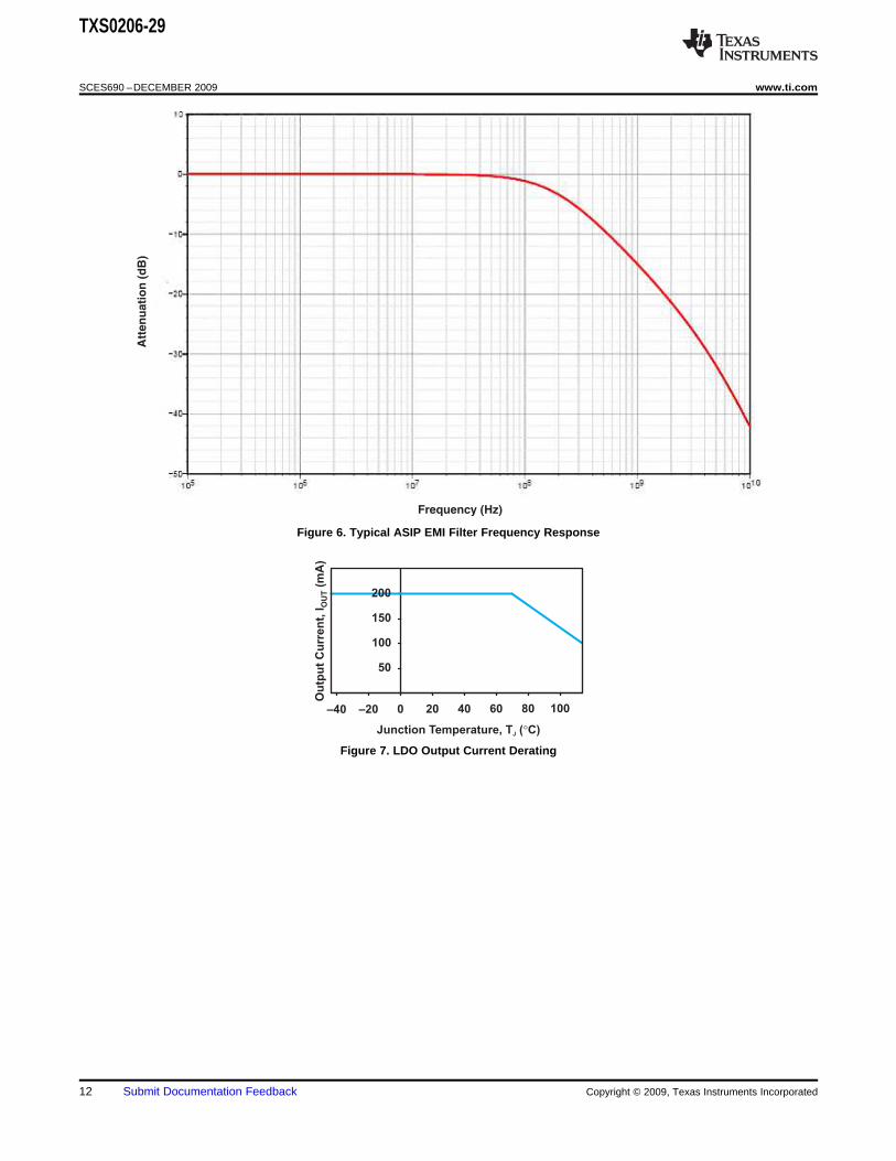
Figure 6. Typical ASIP EMI Filter Frequency Response
Figure 7. LDO Output Current Derating
12 Submit Documentation Feedback Copyright © 2009, Texas Instruments Incorporated

-100
-80
-60
-40
-20
0
20
40
60
80
100
0 1 2 3 4 5
IOUT (mA)
?V O
UT(m
V)
TA = -40°C
TA = 25°C
TA = 85°C
D-200
-160
-120
-80
-40
0
40
80
120
160
200
0 50 100 150 200
IOUT (mA)
?V O
UT(m
V)
TA = -40°C
TA = 25°C
TA = 85°C
D
-2.4
-2.2
-2
-1.8
-1.6
-1.4
-1.2
-1
-0.8
-0.6
-0.4
-0.2
0
3 3.25 3.5 3.75 4 4.25 4.5 4.75 5 5.25 5.5
V IN (V)
?V O
UT(%
)
TA = -40°C
TA = 25°C
TA = 85°C
D
-6
-5
-4
-3
-2
-1
0
1
3 3.25 3.5 3.75 4 4.25 4.5 4.75 5 5.25 5.5V IN (V)
?V O
UT(%
)
TA = -40°C
TA = 25°C
TA = 85°C
D
TXS0206-29
www.ti.com SCES690 –DECEMBER 2009
TYPICAL CHARACTERISTICSLOAD REGULATION LOAD REGULATION, LIGHT LOADS
LINE REGULATION LINE REGULATION(IOUT = 5 mA) (IOUT = 150 mA)
Copyright © 2009, Texas Instruments Incorporated Submit Documentation Feedback 13
0
50
100
150
200
250
0 50 100 150 200
IOUT (mA)
VD
O(m
V)
TA = -40°C
TA = 25°C
TA = 85°C
-4
-3
-2
-1
0
1
2
-40 -15 10 35 60 85
TJ (°C)
?V O
UT(%
)
IOUT = 5 mA
IOUT = 150 mA
IOUT = 50 mA
D
0
50
100
150
200
250
300
0 50 100 150 200
IOUT (mA)
I GN
D(µ
A)
0
25
50
75
100
125
150
175
200
-40 -15 10 35 60 85
TJ (°C)
VD
O(m
V)
IOUT = 5 mA
IOUT = 150 mA
IOUT = 100 mA
TXS0206-29
SCES690 –DECEMBER 2009 www.ti.com
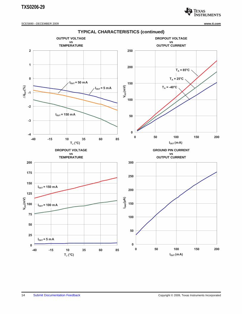
TYPICAL CHARACTERISTICS (continued)OUTPUT VOLTAGE DROPOUT VOLTAGE
vs vsTEMPERATURE OUTPUT CURRENT
DROPOUT VOLTAGE GROUND PIN CURRENTvs vs
TEMPERATURE OUTPUT CURRENT
14 Submit Documentation Feedback Copyright © 2009, Texas Instruments Incorporated
0.30
0.32
0.34
0.36
0.38
0.40
3 3.5 4 4.5 5 5.5
V IN (V)
I OU
T(A
) TA = -40°C TA = 25°C
TA = 85°C
0
50
100
150
200
250
300
-40 -15 10 35 60 85
TJ (°C)
I GN
D(µ
A)
IOUT = 2 mA
IOUT = 150 mA
IOUT = 100 mA
0
1
2
3
4
5
6
7
8
9
10
100
1000
1000
0
1000
00
Frequency (Hz)
Ou
tpu
tN
ois
eD
en
sit
y(µ
V/?
Hz)
-100
-90
-80
-70
-60
-50
-40
-30
-20
-10
1.E+01 1.E+02 1.E+03 1.E+04 1.E+05 1.E+06 1.E+07
Frequency (Hz)
PS
RR
(dB
)
100 mA 200 mA 10 mA
0 mA 50 mA
1 10 1k 10k 100k 1M 10M
TXS0206-29
www.ti.com SCES690 –DECEMBER 2009
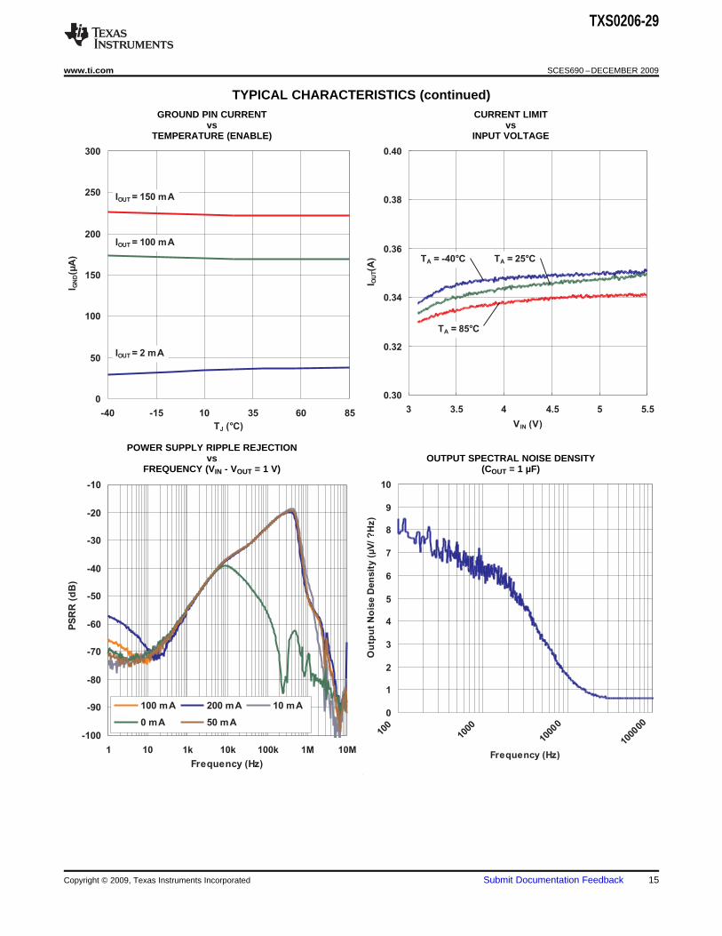
TYPICAL CHARACTERISTICS (continued)GROUND PIN CURRENT CURRENT LIMIT
vs vsTEMPERATURE (ENABLE) INPUT VOLTAGE
POWER SUPPLY RIPPLE REJECTIONvs OUTPUT SPECTRAL NOISE DENSITY
FREQUENCY (VIN - VOUT = 1 V) (COUT = 1 µF)
Copyright © 2009, Texas Instruments Incorporated Submit Documentation Feedback 15

2.85
2.86
2.87
2.88
2.89
2.9
2.91
2.92
2.93
2.94
-0.6 -0.5 -0.4 -0.3 -0.2 -0.1 0 0.1
time (ms)
VO
UT(V
)
3
3.25
3.5
3.75
4
4.25
4.5
4.75
5
5.25
5.5
VIN
(V)
V IN
VOUT
2.50
2.55
2.60
2.65
2.70
2.75
2.80
2.85
2.90
2.95
3.00
-0.35 -0.25 -0.15 -0.05 0.05 0.15
time (ms)
VO
UT(V
)
-0.02
0.00
0.02
0.04
0.06
0.08
0.10
0.12
0.14
0.16
0.18
I OU
T(A
)
IOUT
VOUT
-0.5
0
0.5
1
1.5
2
2.5
3
3.5
-0.001 0 0.001 0.002 0.003 0.004 0.005 0.006
time (s)
VIN,V O
UT(V
)
V IN
VOUT
-0.5
0
0.5
1
1.5
2
2.5
3
3.5
4
-0.1 -0.05 0 0.05 0.1 0.15 0.2 0.25 0.3
time (ms)
VIN,V O
UT(V
)
V IN
VOUT
(COUT = 3 µF)
VOUT
(COUT = 1 µF)
TXS0206-29
SCES690 –DECEMBER 2009 www.ti.com
TYPICAL CHARACTERISTICS (continued)LINE TRANSIENT RESPONSE LOAD TRANSIENT RESPONSE
(COUT = 1 µF) (COUT = 1 µF, VIN = 3.3 V, IOUT = 0 to 100 mA)
POWER-UP/POWER-DOWNTURN-ON RESPONSE (COUT = 1 µF, IOUT = 150 mA)
16 Submit Documentation Feedback Copyright © 2009, Texas Instruments Incorporated

VOH
VOL
From Output Under Test
LOAD CIRCUIT FOR ENABLE/DISABLETIME MEASUREMENT
S1
2 × VCCO
Open
50 k
tPLH tPHL
OutputControl
(low-levelenabling)
OutputWaveform 1
S1 at 2 × VCCO(see Note B)
OutputWaveform 2
S1 at GND(see Note B)
tPZL
tPZH
tPLZ
tPHZ
VCCA/2VCCA/2
VCCI
0 V
VCCO/2VOH
VOL
0 V
0.1 VCCO
VCCO/2
0.9 VCCOVCCO/2
0 V
VCCI
0 V
VCCI/2 VCCI/2
tw
Input
VCCA
VCCO
VOLTAGE WAVEFORMSPROPAGATION DELAY TIMES
VOLTAGE WAVEFORMSPULSE DURATION
VOLTAGE WAVEFORMSENABLE AND DISABLE TIMES
Output
Input
tPZL/tPLZtPHZ/tPZH
2 × VCCOOpen
TEST S1
A. CL includes probe and jig capacitance.B. Waveform 1 is for an output with internal conditions such that the output is low, except when disabled by the output control.
Waveform 2 is for an output with internal conditions such that the output is high, except when disabled by the output control.C. All input pulses are supplied by generators having the following characteristics: PRR10 MHz, ZO = 50 Ω, dv/dt ≥ 1 V/ns.D. The outputs are measured one at a time, with one transition per measurement.E. tPLZ and tPHZ are the same as tdis.F. tPZL and tPZH are the same as ten.G. tPLH and tPHL are the same as tpd.H. VCCI is the VCC associated with the input port.I. VCCO is the VCC associated with the output port.J. All parameters and waveforms are not applicable to all devices.
50 k
1 M15 pF
15 pF
DATA RATE, PULSE DURATION, PROPAGATION DELAY,OUTPUT RISE AND FALL TIME MEASUREMENT USING
A PUSH-PULL DRIVER
VCCOVCCI
DUT
IN OUT
1 M15 pF
DATA RATE, PULSE DURATION, PROPAGATION DELAY,OUTPUT RISE AND FALL TIME MEASUREMENT USING
AN OPEN-DRAIN DRIVER
VCCOVCCI
DUT
IN OUT
VCCI/2 VCCI/2
0.9 VCCOVCCO/2
tr
0.1 VCCO
tf
TXS0206-29
www.ti.com SCES690 –DECEMBER 2009
PARAMETER MEASUREMENT INFORMATION
Figure 8. Load Circuit and Voltage WaveformsN
Copyright © 2009, Texas Instruments Incorporated Submit Documentation Feedback 17

T2
T1
VCCA V O/PCCB
N1
Translator
One-Shot
One-Shot
SDIO-DATAx(B)
R2
BiasSDIO-DATAx(A)
R1
T4
T3
Translator
One-Shot
One-Shot
TXS0206-29
SCES690 –DECEMBER 2009 www.ti.com
PRINCIPLES OF OPERATION
Applications
The TXS0206-29 device is a complete application-specific voltage-translator designed to bridge thedigital-switching compatibility gap and interface logic threshold levels between a micrprocessor with MMC, SD,and Memory Stick™ cards. It is intended to be used in a point-to-point topology when interfacing these devicesthat may or may not be operating at different interface voltages.
Architecture
The CLKA, CLKB, and CLK-f subsystem interfaces consist of a fully-buffered voltage translator design that hasits output transistors to source and sink current optimized for drive strength.
The SDIO lines comprise a semi-buffered auto-direction-sensing based translator architecture (see Figure 9) thatdoes not require a direction-control signal to control the direction of data flow of the A to B ports (or from B to Aports).
Figure 9. Architecture of an SDIO Switch-Type Cell
Each of these bidirectional SDIO channels independently determines the direction of data flow without adirection-control signal. Each I/O pin can be automatically reconfigured as either an input or an output, which ishow this auto-direction feature is realized.
The following two key circuits are employed to facilitate the "switch-type" voltage translation function:1. Integrated pullup resistors to provide dc-bias and drive capabilities2. An N-channel pass-gate transistor topology (with a high RON of ~300 Ω) that ties the A-port to the B-port3. Output one-shot (O.S.) edge-rate accelerator circuitry to detect and accelerate rising edges on the A or B
ports
18 Submit Documentation Feedback Copyright © 2009, Texas Instruments Incorporated
TXS0206-29
www.ti.com SCES690 –DECEMBER 2009
For bidirectional voltage translation, pullup resistors are included on the device for dc current sourcing capability.The VGATE gate bias of the N-channel pass transistor is set at a level that optimizes the switch characteristics formaximum data rate as well as minimal static supply leakage. Data can flow in either direction without guidancefrom a control signal.
The edge-rate acceleration circuitry speeds up the output slew rate by monitoring the input edge for transitions,helping maintain the data rate through the device.
During a low-to-high signal rising-edge, the O.S. circuits turn on the PMOS transistors (T1, T3) and its associateddriver output resistance of the driver is decreased to approximately 50 Ω to 70 Ω during this acceleration phaseto increase the current drive capability of the driver for approximately 30 ns or 95% of the input edge, whicheveroccurs first. This edge-rate acceleration provides high ac drive by bypassing the internal pullup resistors duringthe low-to-high transition to speed up the rising-edge signal.
During a high-to-low signal falling-edge, the O.S. circuits turn on the NMOS transistors (T2, T4) and its associateddriver output resistance of the driver is decreased to approximately 50 Ω to 70 Ω during this acceleration phaseto increase the current drive capability of the driver for approximately 30 ns or 95% of the input edge, whicheveroccurs first.
To minimize dynamic ICC and the possibility of signal contention, the user should wait for the O.S. circuit toturn-off before applying a signal in the opposite direction. The worst-case duration is equal to the minimumpulse-width number provided in the Timing Requirements section of this data sheet.
Once the O.S. is triggered and switched off, both the A and B ports must go to the same state (i.e. both High orboth Low) for the one-shot to trigger again. In a DC state, the output drivers maintain a Low state through thepass transistor. The output drivers maintain a High through the "smart pullup resistors" that dynamically changevalue based on whether a Low or a High is being passed through the SDIO lines, as follows:• RPU1 and RPU2 values are a nominal 40 kΩ when the output is driving a low• RPU1 and RPU2 values are a nominal 4 kΩ when the output is driving a high• RPU1 and RPU2 values are a nominal 70 kΩ when the device is disabled via the EN pin or by pulling the either
VCCA or VCCBO/P to 0 V.
The reason for using these "smart" pullup resistors is to allow the TXS0206-29 to realize a lower static powerconsumption (when the I/Os are low), support lower VOL values for the same size pass-gate transistor, andimproved simultaneous switching performance.
Input Driver Requirements
The continuous dc-current "sinking" capability is determined by the external system-level driver interfaced to theSDIO pins. Since the high bandwidth of these bidirectional SDIO circuits necessitates the need for a port toquickly change from an input to an output (and vice-vera), they have a modest dc-current "sourcing" capability ofhundreds of micro-Amps, as determined by the smart pullup resistor values.
The fall time (tfA, tfB) of a signal depends on the edge rate and output impedance of the external device drivingthe SDIO I/Os, as well as the capacitive loading on these lines.
Similarly, the tpd and max data rates also depend on the output impedance of the external driver. The values fortfA, tfB, tpd, and maximum data rates in the data sheet assume that the output impedance of the external driver isless than 50 Ω.
Output Load Considerations
TI recommends careful PCB layout practices with short PCB trace lengths to avoid excessive capacitive loadingand to ensure that proper O.S. triggering takes place. PCB signal trace-lengths should be kept short enoughsuch that the round trip delay of any reflection is less than the one-shot duration. This improves signal integrityby ensuring that any reflection sees a low impedance at the driver. The O.S. circuits have been designed to stayon for approximately 30 ns. The maximum capacitance of the lumped load that can be driven also dependsdirectly on the one-shot duration. With very heavy capacitive loads, the one-shot can time-out before the signal isdriven fully to the positive rail. The O.S. duration has been set to best optimize trade-offs between dynamic ICC,load driving capability, and maximum bit-rate considerations. Both PCB trace length and connectors add to thecapacitance that the TXS0206-29 SDIO output sees, so it is recommended that this lumped-load capacitance beconsidered and kept below 50 pF to avoid O.S. retriggering, bus contention, output signal oscillations, or otheradverse system-level affects.
Copyright © 2009, Texas Instruments Incorporated Submit Documentation Feedback 19

TXS0206-29
SCES690 –DECEMBER 2009 www.ti.com
When using the TXS0206-29 device with MMCs, SD, and Memory Stick™ to ensure that a valid receiver inputvoltage high (VIH) is achieved, the value of any pulldown resistors (external or internal to a memory card) mustnot be >10-kΩ value. The impact of adding too heavy a pulldown resistor (i.e. <10-kΩ value) to the data andcommand lines of the TXS0206-29 device and the resulting 4-kΩ pullup & 10-kΩ pulldown voltage dividernetwork has a direct impact on the VIH of the signal being sent into the memory card and its associated logic.
The resulting VIH voltage for the 10-kΩ pulldown resistor value would be:VCC × 10 kΩ / (10 kΩ+ 4 kΩ) = 0.714 × VCC
This is marginally above a valid input high voltage for a 1.8-V signal (i.e., 0.65 × VCC).
The resulting VIH voltage for 20-kΩ pulldown resistor value would be:VCC × 20 kΩ / (20 kΩ + 4 kΩ) = 0.833 × VCC
Which is above the valid input high voltage for a 1.8-V signal of 0.65 × VCC.
.
20 Submit Documentation Feedback Copyright © 2009, Texas Instruments Incorporated

PACKAGE OPTION ADDENDUM
www.ti.com 18-Jun-2018
Addendum-Page 1
PACKAGING INFORMATION
Orderable Device Status(1)
Package Type PackageDrawing
Pins PackageQty
Eco Plan(2)
Lead/Ball Finish(6)
MSL Peak Temp(3)
Op Temp (°C) Device Marking(4/5)
Samples
TXS0206-29YFPRB ACTIVE DSBGA YFP 20 3000 Green (RoHS& no Sb/Br)
SNAGCU Level-1-260C-UNLIM -40 to 85 (3V, 3V2)
(1) The marketing status values are defined as follows:ACTIVE: Product device recommended for new designs.LIFEBUY: TI has announced that the device will be discontinued, and a lifetime-buy period is in effect.NRND: Not recommended for new designs. Device is in production to support existing customers, but TI does not recommend using this part in a new design.PREVIEW: Device has been announced but is not in production. Samples may or may not be available.OBSOLETE: TI has discontinued the production of the device.
(2) RoHS: TI defines "RoHS" to mean semiconductor products that are compliant with the current EU RoHS requirements for all 10 RoHS substances, including the requirement that RoHS substancedo not exceed 0.1% by weight in homogeneous materials. Where designed to be soldered at high temperatures, "RoHS" products are suitable for use in specified lead-free processes. TI mayreference these types of products as "Pb-Free".RoHS Exempt: TI defines "RoHS Exempt" to mean products that contain lead but are compliant with EU RoHS pursuant to a specific EU RoHS exemption.Green: TI defines "Green" to mean the content of Chlorine (Cl) and Bromine (Br) based flame retardants meet JS709B low halogen requirements of <=1000ppm threshold. Antimony trioxide basedflame retardants must also meet the <=1000ppm threshold requirement.
(3) MSL, Peak Temp. - The Moisture Sensitivity Level rating according to the JEDEC industry standard classifications, and peak solder temperature.
(4) There may be additional marking, which relates to the logo, the lot trace code information, or the environmental category on the device.
(5) Multiple Device Markings will be inside parentheses. Only one Device Marking contained in parentheses and separated by a "~" will appear on a device. If a line is indented then it is a continuationof the previous line and the two combined represent the entire Device Marking for that device.
(6) Lead/Ball Finish - Orderable Devices may have multiple material finish options. Finish options are separated by a vertical ruled line. Lead/Ball Finish values may wrap to two lines if the finishvalue exceeds the maximum column width.
Important Information and Disclaimer:The information provided on this page represents TI's knowledge and belief as of the date that it is provided. TI bases its knowledge and belief on informationprovided by third parties, and makes no representation or warranty as to the accuracy of such information. Efforts are underway to better integrate information from third parties. TI has taken andcontinues to take reasonable steps to provide representative and accurate information but may not have conducted destructive testing or chemical analysis on incoming materials and chemicals.TI and TI suppliers consider certain information to be proprietary, and thus CAS numbers and other limited information may not be available for release.
In no event shall TI's liability arising out of such information exceed the total purchase price of the TI part(s) at issue in this document sold by TI to Customer on an annual basis.

TAPE AND REEL INFORMATION
*All dimensions are nominal
Device PackageType
PackageDrawing
Pins SPQ ReelDiameter
(mm)
ReelWidth
W1 (mm)
A0(mm)
B0(mm)
K0(mm)
P1(mm)
W(mm)
Pin1Quadrant
TXS0206-29YFPRB DSBGA YFP 20 3000 180.0 8.4 1.66 2.06 0.56 4.0 8.0 Q1
PACKAGE MATERIALS INFORMATION
www.ti.com 15-Apr-2017
Pack Materials-Page 1
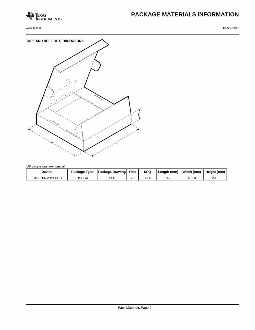
*All dimensions are nominal
Device Package Type Package Drawing Pins SPQ Length (mm) Width (mm) Height (mm)
TXS0206-29YFPRB DSBGA YFP 20 3000 182.0 182.0 20.0
PACKAGE MATERIALS INFORMATION
www.ti.com 15-Apr-2017
Pack Materials-Page 2
www.ti.com
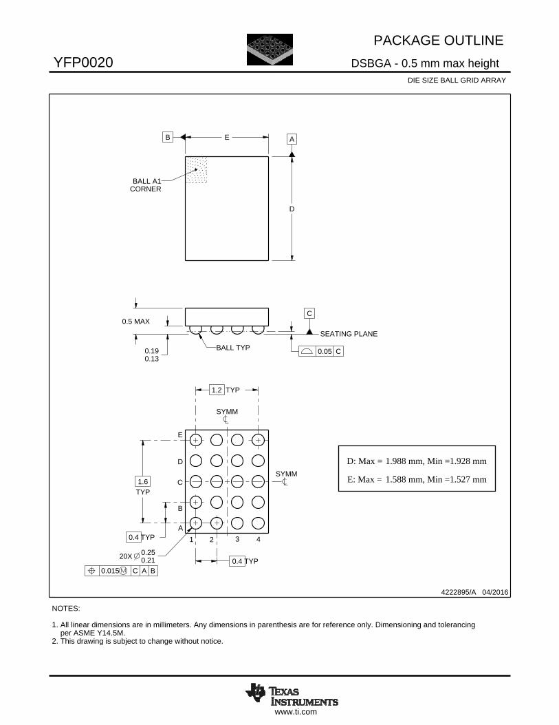
PACKAGE OUTLINE
C0.5 MAX
0.190.13
1.6TYP
1.2 TYP
0.4 TYP
0.4 TYP20X 0.25
0.21
B E A
D
4222895/A 04/2016
DSBGA - 0.5 mm max heightYFP0020DIE SIZE BALL GRID ARRAY
NOTES: 1. All linear dimensions are in millimeters. Any dimensions in parenthesis are for reference only. Dimensioning and tolerancing per ASME Y14.5M.2. This drawing is subject to change without notice.
BALL A1CORNER
SEATING PLANE
BALL TYP 0.05 C
A
B
C
D
1 2 3
0.015 C A B
E
4
SYMM
SYMM
SCALE 7.000
D: Max =
E: Max =
1.988 mm, Min =
1.588 mm, Min =
1.928 mm
1.527 mm

www.ti.com
EXAMPLE BOARD LAYOUT
20X ( )0.23
(0.4) TYP
(0.4) TYP
( )METAL
0.23 0.05 MAX
SOLDER MASKOPENING
METAL UNDERSOLDER MASK
( )SOLDER MASKOPENING
0.23
0.05 MIN
4222895/A 04/2016
DSBGA - 0.5 mm max heightYFP0020DIE SIZE BALL GRID ARRAY
NOTES: (continued) 3. Final dimensions may vary due to manufacturing tolerance considerations and also routing constraints. For more information, see Texas Instruments literature number SNVA009 (www.ti.com/lit/snva009).
SOLDER MASK DETAILSNOT TO SCALE
SYMM
SYMM
LAND PATTERN EXAMPLESCALE:25X
A
B
C
D
1 2 3 4
E
NON-SOLDER MASKDEFINED
(PREFERRED)
SOLDER MASKDEFINED

www.ti.com
EXAMPLE STENCIL DESIGN
(0.4) TYP
(0.4) TYP
20X ( 0.25) (R ) TYP0.05
METALTYP
4222895/A 04/2016
DSBGA - 0.5 mm max heightYFP0020DIE SIZE BALL GRID ARRAY
NOTES: (continued) 4. Laser cutting apertures with trapezoidal walls and rounded corners may offer better paste release.
SYMM
SYMM
SOLDER PASTE EXAMPLEBASED ON 0.1 mm THICK STENCIL
SCALE:30X
A
B
C
D
1 2 3
E
4
IMPORTANT NOTICE
Texas Instruments Incorporated (TI) reserves the right to make corrections, enhancements, improvements and other changes to itssemiconductor products and services per JESD46, latest issue, and to discontinue any product or service per JESD48, latest issue. Buyersshould obtain the latest relevant information before placing orders and should verify that such information is current and complete.TI’s published terms of sale for semiconductor products (http://www.ti.com/sc/docs/stdterms.htm) apply to the sale of packaged integratedcircuit products that TI has qualified and released to market. Additional terms may apply to the use or sale of other types of TI products andservices.Reproduction of significant portions of TI information in TI data sheets is permissible only if reproduction is without alteration and isaccompanied by all associated warranties, conditions, limitations, and notices. TI is not responsible or liable for such reproduceddocumentation. Information of third parties may be subject to additional restrictions. Resale of TI products or services with statementsdifferent from or beyond the parameters stated by TI for that product or service voids all express and any implied warranties for theassociated TI product or service and is an unfair and deceptive business practice. TI is not responsible or liable for any such statements.Buyers and others who are developing systems that incorporate TI products (collectively, “Designers”) understand and agree that Designersremain responsible for using their independent analysis, evaluation and judgment in designing their applications and that Designers havefull and exclusive responsibility to assure the safety of Designers' applications and compliance of their applications (and of all TI productsused in or for Designers’ applications) with all applicable regulations, laws and other applicable requirements. Designer represents that, withrespect to their applications, Designer has all the necessary expertise to create and implement safeguards that (1) anticipate dangerousconsequences of failures, (2) monitor failures and their consequences, and (3) lessen the likelihood of failures that might cause harm andtake appropriate actions. Designer agrees that prior to using or distributing any applications that include TI products, Designer willthoroughly test such applications and the functionality of such TI products as used in such applications.TI’s provision of technical, application or other design advice, quality characterization, reliability data or other services or information,including, but not limited to, reference designs and materials relating to evaluation modules, (collectively, “TI Resources”) are intended toassist designers who are developing applications that incorporate TI products; by downloading, accessing or using TI Resources in anyway, Designer (individually or, if Designer is acting on behalf of a company, Designer’s company) agrees to use any particular TI Resourcesolely for this purpose and subject to the terms of this Notice.TI’s provision of TI Resources does not expand or otherwise alter TI’s applicable published warranties or warranty disclaimers for TIproducts, and no additional obligations or liabilities arise from TI providing such TI Resources. TI reserves the right to make corrections,enhancements, improvements and other changes to its TI Resources. TI has not conducted any testing other than that specificallydescribed in the published documentation for a particular TI Resource.Designer is authorized to use, copy and modify any individual TI Resource only in connection with the development of applications thatinclude the TI product(s) identified in such TI Resource. NO OTHER LICENSE, EXPRESS OR IMPLIED, BY ESTOPPEL OR OTHERWISETO ANY OTHER TI INTELLECTUAL PROPERTY RIGHT, AND NO LICENSE TO ANY TECHNOLOGY OR INTELLECTUAL PROPERTYRIGHT OF TI OR ANY THIRD PARTY IS GRANTED HEREIN, including but not limited to any patent right, copyright, mask work right, orother intellectual property right relating to any combination, machine, or process in which TI products or services are used. Informationregarding or referencing third-party products or services does not constitute a license to use such products or services, or a warranty orendorsement thereof. Use of TI Resources may require a license from a third party under the patents or other intellectual property of thethird party, or a license from TI under the patents or other intellectual property of TI.TI RESOURCES ARE PROVIDED “AS IS” AND WITH ALL FAULTS. TI DISCLAIMS ALL OTHER WARRANTIES ORREPRESENTATIONS, EXPRESS OR IMPLIED, REGARDING RESOURCES OR USE THEREOF, INCLUDING BUT NOT LIMITED TOACCURACY OR COMPLETENESS, TITLE, ANY EPIDEMIC FAILURE WARRANTY AND ANY IMPLIED WARRANTIES OFMERCHANTABILITY, FITNESS FOR A PARTICULAR PURPOSE, AND NON-INFRINGEMENT OF ANY THIRD PARTY INTELLECTUALPROPERTY RIGHTS. TI SHALL NOT BE LIABLE FOR AND SHALL NOT DEFEND OR INDEMNIFY DESIGNER AGAINST ANY CLAIM,INCLUDING BUT NOT LIMITED TO ANY INFRINGEMENT CLAIM THAT RELATES TO OR IS BASED ON ANY COMBINATION OFPRODUCTS EVEN IF DESCRIBED IN TI RESOURCES OR OTHERWISE. IN NO EVENT SHALL TI BE LIABLE FOR ANY ACTUAL,DIRECT, SPECIAL, COLLATERAL, INDIRECT, PUNITIVE, INCIDENTAL, CONSEQUENTIAL OR EXEMPLARY DAMAGES INCONNECTION WITH OR ARISING OUT OF TI RESOURCES OR USE THEREOF, AND REGARDLESS OF WHETHER TI HAS BEENADVISED OF THE POSSIBILITY OF SUCH DAMAGES.Unless TI has explicitly designated an individual product as meeting the requirements of a particular industry standard (e.g., ISO/TS 16949and ISO 26262), TI is not responsible for any failure to meet such industry standard requirements.Where TI specifically promotes products as facilitating functional safety or as compliant with industry functional safety standards, suchproducts are intended to help enable customers to design and create their own applications that meet applicable functional safety standardsand requirements. Using products in an application does not by itself establish any safety features in the application. Designers mustensure compliance with safety-related requirements and standards applicable to their applications. Designer may not use any TI products inlife-critical medical equipment unless authorized officers of the parties have executed a special contract specifically governing such use.Life-critical medical equipment is medical equipment where failure of such equipment would cause serious bodily injury or death (e.g., lifesupport, pacemakers, defibrillators, heart pumps, neurostimulators, and implantables). Such equipment includes, without limitation, allmedical devices identified by the U.S. Food and Drug Administration as Class III devices and equivalent classifications outside the U.S.TI may expressly designate certain products as completing a particular qualification (e.g., Q100, Military Grade, or Enhanced Product).Designers agree that it has the necessary expertise to select the product with the appropriate qualification designation for their applicationsand that proper product selection is at Designers’ own risk. Designers are solely responsible for compliance with all legal and regulatoryrequirements in connection with such selection.Designer will fully indemnify TI and its representatives against any damages, costs, losses, and/or liabilities arising out of Designer’s non-compliance with the terms and provisions of this Notice.
Mailing Address: Texas Instruments, Post Office Box 655303, Dallas, Texas 75265Copyright © 2018, Texas Instruments Incorporated
Related Documents