eScholarship provides open access, scholarly publishing services to the University of California and delivers a dynamic research platform to scholars worldwide. University of California Peer Reviewed Title: Scanning transmission electron microscopy of gate stacks with HfO2 dielectrics and TiN electrodes Author: Agustin, Melody P. Fonseca, Leo R. C. Hooker, Jacob C. Stemmer, Susanne , University of California Santa Barbara Publication Date: 01-01-2005 Publication Info: Postprints, UC Santa Barbara Permalink: http://escholarship.org/uc/item/6rf7c5q0 Additional Info: Copyright by American Institute of Physics (AIP) . Published Web Location: http://scitation.aip.org/getabs/servlet/GetabsServlet? prog=normal&id=APPLAB000087000012121909000001&idtype=cvips&gifs=yes Keywords: Scanning transmission electron microscopy, gate dielectric, HfO2, STEM Abstract: High-angle annular dark-field (HAADF) imaging and electron energy-loss spectroscopy (EELS) in scanning transmission electron microscopy were used to investigate HfO2 gate dielectrics grown by atomic layer deposition on Si substrates, and their interfaces with TiN electrodes and silicon, as a function of annealing temperature. Annealing at high temperatures (900 °C) caused significant roughening of both bottom (substrate) and top (electrode) interface. At the bottom interface, HAADF images showed clusters of Hf atoms that protruded into the interfacial SiO2 layer. Low- loss EELS established that even crystalline HfO2 films exposed to relative high temperatures (700 °C) exhibited significant differences in their electronic structure relative to bulk HfO2. Further annealing caused the electronic structure to more closely resemble that of bulk HfO2, with the most significant change due to annealing with the TiN electrode.

Welcome message from author
This document is posted to help you gain knowledge. Please leave a comment to let me know what you think about it! Share it to your friends and learn new things together.
Transcript

eScholarship provides open access, scholarly publishingservices to the University of California and delivers a dynamicresearch platform to scholars worldwide.
University of California
Peer Reviewed
Title:Scanning transmission electron microscopy of gate stacks with HfO2 dielectrics and TiNelectrodes
Author:Agustin, Melody P.Fonseca, Leo R. C.Hooker, Jacob C.Stemmer, Susanne, University of California Santa Barbara
Publication Date:01-01-2005
Publication Info:Postprints, UC Santa Barbara
Permalink:http://escholarship.org/uc/item/6rf7c5q0
Additional Info:Copyright by American Institute of Physics (AIP).
Published Web Location:http://scitation.aip.org/getabs/servlet/GetabsServlet?prog=normal&id=APPLAB000087000012121909000001&idtype=cvips&gifs=yes
Keywords:Scanning transmission electron microscopy, gate dielectric, HfO2, STEM
Abstract:High-angle annular dark-field (HAADF) imaging and electron energy-loss spectroscopy (EELS) inscanning transmission electron microscopy were used to investigate HfO2 gate dielectrics grownby atomic layer deposition on Si substrates, and their interfaces with TiN electrodes and silicon, asa function of annealing temperature. Annealing at high temperatures (900 °C) caused significantroughening of both bottom (substrate) and top (electrode) interface. At the bottom interface,HAADF images showed clusters of Hf atoms that protruded into the interfacial SiO2 layer. Low-loss EELS established that even crystalline HfO2 films exposed to relative high temperatures(700 °C) exhibited significant differences in their electronic structure relative to bulk HfO2. Furtherannealing caused the electronic structure to more closely resemble that of bulk HfO2, with themost significant change due to annealing with the TiN electrode.

1
Scanning transmission electron microscopy of gate stacks with HfO2
dielectrics and TiN electrodes
Melody P. Agustin
Materials Department, University of California, Santa Barbara, CA 93106-5050
Leonardo R. C. Fonseca
Freescale Semiconductores Brasil Ltda, Jaguariúna 13820-000, Brazil
Jacob C. Hooker
CMOS Module Integration, Philips Research Leuven, B-3001 Leuven, Belgium
Susanne Stemmera)
Materials Department, University of California, Santa Barbara, CA 93106-5050
a) Electronic mail: [email protected]

2
ABSTRACT
High-angle annular dark-field (HAADF) imaging and electron energy-loss spectroscopy
(EELS) in scanning transmission electron microscopy were used to investigate HfO2 gate
dielectrics grown by atomic layer deposition on Si substrates, and their interfaces with TiN
electrodes and silicon, as a function of annealing temperature. Annealing at high temperatures
(900 °C) caused significant roughening of both bottom (substrate) and top (electrode) interface.
At the bottom interface, HAADF images showed clusters of Hf atoms that protruded into the
interfacial SiO2 layer. Low-loss EELS established that even crystalline HfO2 films exposed to
relative high temperatures (700 °C) exhibited significant differences in their electronic structure
relative to bulk HfO2. Further annealing caused the electronic structure to more closely resemble
that of bulk HfO2, with the most significant change due to annealing with the TiN electrode.
3
Continued scaling of feature sizes in complementary metal-oxide-semiconductor
(CMOS) devices will require the replacement of SiO2 with gate dielectrics that have a higher
dielectric constant (k), such as HfO2. In addition, the heavily doped polycrystalline silicon gate
electrode may have to be replaced with metal electrodes. Midgap gate electrode metals, such as
TiN, are being extensively investigated [1-4]. The metal/dielectric and the dielectric/Si interface
determine the CMOS device performance, including channel mobility and threshold voltage. To
date, the chemistry and structure of these new interfaces remain poorly understood. For
example, the precise chemistry of SiO2-like interfacial layers formed between ZrO2 or HfO2 gate
dielectrics and the Si substrate interface under oxidizing deposition conditions is still under
debate. Electrical measurements show that the dielectric constant of these interfacial layers is
greater than that of pure, bulk SiO2 and it has been suggested that the interfacial layer is
substoichiometric SiO2 or a metal silicate [5-7]. Recent medium energy ion-scattering and
electron energy-loss spectroscopy (EELS) studies found no evidence for silicate formation [8,9].
At the HfO2/TiN interface, intermixing has been reported by some authors [2], whereas others
report a thermally stable interface but with significant roughening [4].
The goal of this paper is an improved understanding of the structure and bonding in HfO2
layers and their interfaces with the Si substrate and TiN electrodes as a function of annealing
temperature. We use scanning transmission electron microscopy (STEM) based techniques, in
particular high-angle annular dark-field (HAADF) imaging and EELS. As the signal at low
energy losses is significantly delocalized, relatively thick HfO2 films (~ 13 nm) were
investigated to allow low-loss EELS to be recorded from the film without the influence from
adjacent layers.
4
HfO2 gate dielectrics were grown on n-type Si substrates (cleaned using the IMEC clean
[10]) by atomic layer deposition (ALD) using alternating cycles of HfCl4 and H2O with N2
carrier gas. A post-deposition anneal in O2 at 700 °C for 60 seconds was carried out. 20 nm
thick TiN capping layers were deposited by ALD (TiCl4 and NH3 at 350 °C) followed by another
20 nm of TiN grown by DC sputtering. These samples will be referred to as “as-deposited”.
Selected samples were exposed to rapid thermal anneals (RTA) in N2 ambient for 30 s at 700 °C,
800 °C, and 900 °C, respectively.
TEM samples were prepared by standard sample preparation techniques with ion milling
using 3.3 kV Ar ions as the final step. A monoclinic HfO2 powder (99.9% purity with Zr < 50
ppm, Alfa Aesar) was used as a reference sample for EELS. Conventional high-resolution
transmission electron microscopy (HRTEM), HAADF imaging and EELS were performed using
a field-emission TEM (Tecnai F30U, Cs = 0.52 mm) operated at 300 kV. The probe size for
EELS and HAADF was about 2 – 3 Å. EELS spectra were recoded using a Gatan Enfina 1000
spectrometer. The energy resolution (full-width at half-maximum of the zero-loss peak) was
about 0.85 – 0.90 eV. Core-loss EELS spectra of N K-, Ti L2,3- and O K-edge were also
recorded.
HRTEM and HAADF showed that HfO2 and TiN were polycrystalline in all samples.
The HfO2 grain sizes were larger than the film thickness even in the as-deposited sample (note
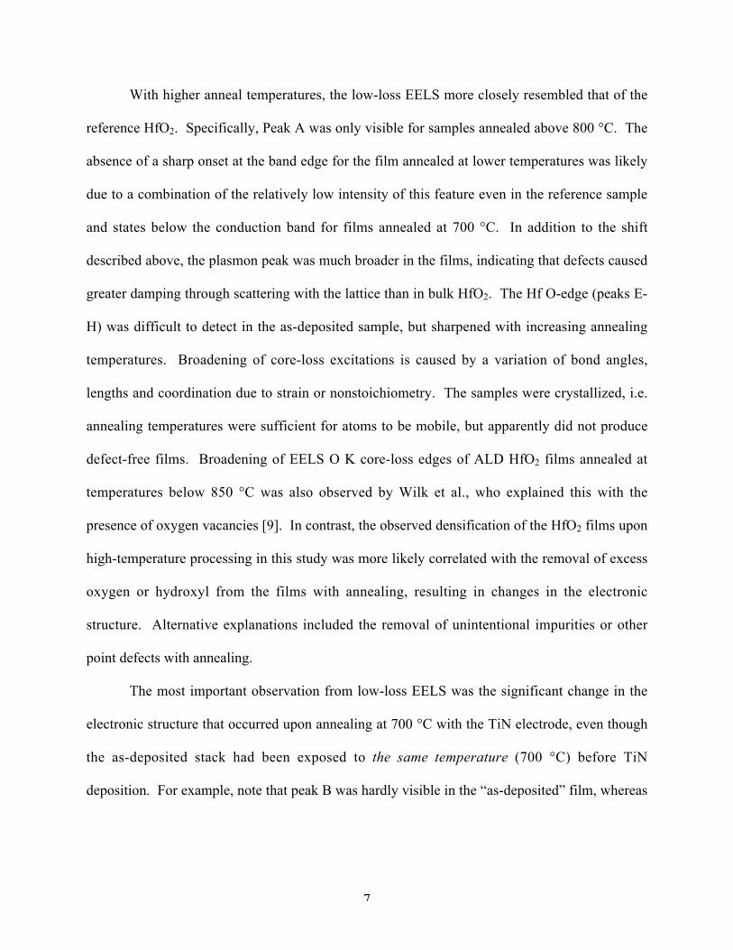
that this sample was exposed to a 700 °C anneal). Figure 1 shows HAADF images of the 800 °C
and the 900 °C annealed gate stack, respectively. For thin samples, the intensity in the HAADF
images is approximately proportional to the atomic number Z2, so that the HfO2 layer appeared
bright in these images, whereas the thin (1.3-1.5 nm) interfacial SiO2-like layer appeared dark.
Layer thicknesses were determined from inflection points of first derivatives of intensity line

5
profiles across the HAADF images [11]. The HfO2 film thickness in the gate stacks annealed up
to 800 °C was about 13.5 nm, while the HfO2 film thickness in the 900 °C gate stack was ~ 12
nm, indicating some densification. Furthermore, roughening of the interfaces with TiN and SiO2
is observed at 900 °C [Fig, 1(b)], which made it more difficult to determine the exact HfO2
thickness. The interfacial roughness was not an imaging artifact because the Si lattice was
visible, the Si/SiO2 interface abrupt and both showed uniform contrast. The
roughening/interdiffusion was more severe at the top (TiN) interface and caused an overlap of
the HfO2 and the TiN grains along the direction of the electron beam. The length scale of the
roughening was smaller than the average HfO2 grain size (note that Fig. 1(b) shows a single
HfO2 grain). Roughening may be due to reaction, intermixing or instability of the interface
plane. Ti L2,3 - fine structures in EELS (not shown) of the overlapping regions resembled those
in TiN, with no crystal field splitting as expected for TiO2. However, other oxides of Ti were
more difficult to distinguish. Thus, the driving force for the roughening/interdiffusion at this
interface is poorly understood.
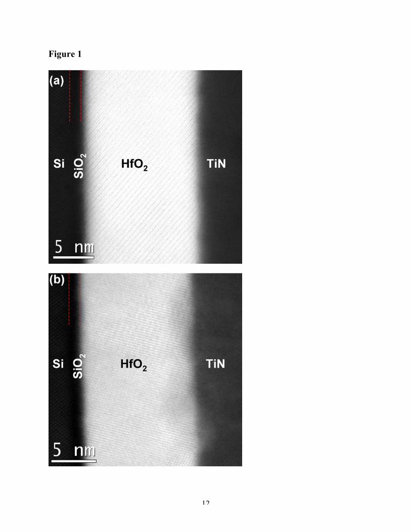
To further investigate the roughening of the bottom interface, Fig. 2 shows a higher
magnification HAADF image of this interface in the 900 °C annealed stack and line intensity
profiles taken from different regions. Along this interface, HAADF images showed clusters of
bright intensity within the SiO2-like layer (circled in Fig. 2), which indicated the presence of
heavy Hf clusters. These Hf clusters were found protruding from the HfO2 layer, whereas no Hf
clusters were observed next to the Si. Similar observations have been reported by others [12].
Clusters appeared to be at least several nm spaced apart, but this may also be due to limited
sensitivity of this method to atoms located at greater depth along the beam direction in an
amorphous matrix [13]. An intensity profile [Fig. 2(b)] showed that the intensity attributed to Hf

6
clusters was significantly above the background noise in the SiO2-like layer. Figure 2 (c) shows
intensity profiles across the SiO2/HfO2 interface. The profile along line 2 in Fig. 2(a) showed
that the change in intensity at the interface was not a step function, which was due to interfacial
roughness convoluted with the finite probe width [11]. The profile along line 3 exhibited an
additional shoulder due to presence of heavy Hf clusters (arrow in Fig. 2(c)).
To investigate changes in the electronic structure of HfO2 films as a function of annealing
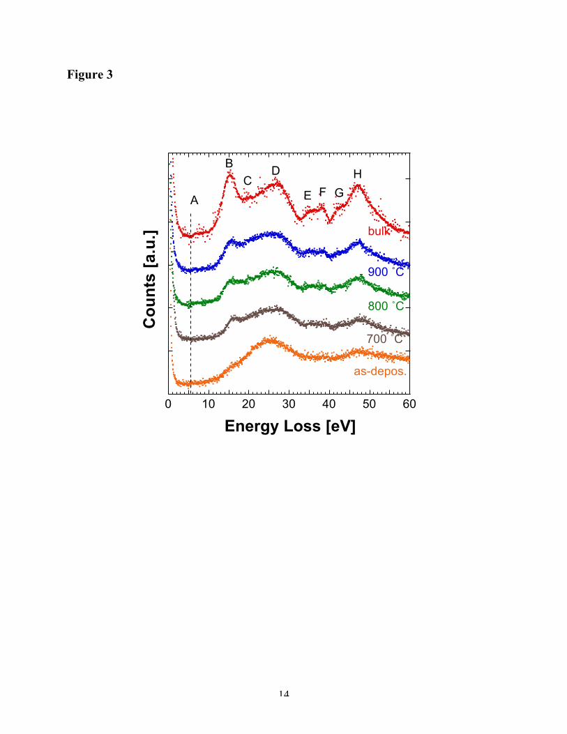
temperature, low-loss EELS spectra were recorded from the center of the HfO2 films and from
the HfO2 reference powder (Fig. 3). In the reference HfO2, the energy-losses of the peaks (in
eV) were ~ 5.6 (A), ~ 15.5 (B), ~ 19 (C), ~ 26.6 (D), 35 (E), ~ 37 (F), ~ 42 (G), and ~ 47 eV (H).
The low-loss EELS of the HfO2 films showed no additional features; therefore the signal
originated from the HfO2 film only.
Low-loss energy loss features (< 30 eV) have been investigated by several authors for the
chemically and structurally similar ZrO2 [14-18]. Peak A corresponded to the energy of the
optical band gap (~ 5.6 – 5.8 eV [19,20]), whereas feature at higher energy losses (peaks E-H)
were due to the Hf O-edge. Some debate exists in the literature as to which of the strong peaks
(B and/or D) corresponds to the plasmon excitation. Due to its strength in the as-deposited
sample, and the fact that it shifted to higher energy losses with increasing annealing
temperatures, we assigned peak D to a plasmon excitation. With this assignment, peak B was
either a plasmon peak [17] or a single electron interband transition between O 2p and Hf 5d [15].
The difference in the plasmon energy (D) of almost 2 eV between the HfO2 reference sample and
the as-deposited film could be explained with the low intensity of B in the films. For example,
interband transitions below plasmon peaks shift the plasmon to higher energies [21].
7
With higher anneal temperatures, the low-loss EELS more closely resembled that of the
reference HfO2. Specifically, Peak A was only visible for samples annealed above 800 °C. The
absence of a sharp onset at the band edge for the film annealed at lower temperatures was likely
due to a combination of the relatively low intensity of this feature even in the reference sample
and states below the conduction band for films annealed at 700 °C. In addition to the shift
described above, the plasmon peak was much broader in the films, indicating that defects caused
greater damping through scattering with the lattice than in bulk HfO2. The Hf O-edge (peaks E-
H) was difficult to detect in the as-deposited sample, but sharpened with increasing annealing
temperatures. Broadening of core-loss excitations is caused by a variation of bond angles,
lengths and coordination due to strain or nonstoichiometry. The samples were crystallized, i.e.
annealing temperatures were sufficient for atoms to be mobile, but apparently did not produce
defect-free films. Broadening of EELS O K core-loss edges of ALD HfO2 films annealed at
temperatures below 850 °C was also observed by Wilk et al., who explained this with the
presence of oxygen vacancies [9]. In contrast, the observed densification of the HfO2 films upon
high-temperature processing in this study was more likely correlated with the removal of excess
oxygen or hydroxyl from the films with annealing, resulting in changes in the electronic
structure. Alternative explanations included the removal of unintentional impurities or other
point defects with annealing.
The most important observation from low-loss EELS was the significant change in the
electronic structure that occurred upon annealing at 700 °C with the TiN electrode, even though
the as-deposited stack had been exposed to the same temperature (700 °C) before TiN
deposition. For example, note that peak B was hardly visible in the “as-deposited” film, whereas

8
it is visible in the film annealed with TiN. This result indicated that the TiN electrode acted as a
sink for impurities or excess oxygen, similar to what was observed for Ti electrodes [22].
In summary, crystalline HfO2 films exposed to relative high temperatures did not possess
bulk electronic structure, as exhibited by the broadening of interband and core-loss transitions
and the absence of a sharp onset at the band edge. Annealing to higher temperatures caused the
electronic structure to more closely resemble that of bulk HfO2, although features were still
broader in the films. Changes in the point defect chemistry were likely responsible for a more
bulk-like electronic structure in films annealed at higher temperatures. In particular, annealing
with the TiN electrode improved the electronic structure. High-temperature processing was,
however, accompanied by roughening of both bottom (substrate) and top (electrode) interface.
At the bottom interface, clusters of Hf atoms were found to protrude into the interfacial SiO2
layer, possibly increasing the apparent permittivity of this interfacial layer compared to a pure,
smooth SiO2 layer. No Hf was found near the Si substrate within the detection limit of HAADF,
so Hf apparently did not rapidly diffuse into the SiO2.
M.P.A. thanks Drs. Dmitri Klenov and Steffen Schmidt for help with the microscope
operation and SRCEA/Intel for a fellowship. This research was supported by SRC.

9
REFERENCES
1 R. Chau, S. Datta, M. Doczy, B. Doyle, J. Kavalieros, and M. Metz, IEEE Electron Dev.
Lett. 25, 408-410 (2004).
2 J. K. Schaeffer, S. B. Samavedam, D. C. Gilmer, V. Dhandapani, P. J. Tobin, J. Mogab,
B.-Y. Nguyen, B. E. White, S. Dakshina-Murthy, R. S. Rai, Z.-X. Jiang, R. Martin, M. V.
Raymond, M. Zavala, L. B. La, J. A. Smith, R. Garcia, D. Roan, M. Kottke, and R. B.
Gregory, J. Vac. Sci. & Technol. B 21, 11-17 (2003).
3 J. Westlinder, T. Schram, L. Pantisano, E. Cartier, A. Kerber, G. S. Lujan, J. Olsson, and
G. Groeseneken, IEEE Electron Dev. Lett. 24, 550-552 (2003).
4 P. S. Lysaght, J. J. Peterson, B. Foran, C. D. Young, G. Bersuker, and H. R. Huff, Mater.
Sci. Semicond. Proc. 7, 259-263 (2004).
5 S. Sayan, S. Aravamudhan, B. W. Busch, W. H. Schulte, F. Cosandey, G. D. Wilk, T.
Gustafsson, and E. Garfunkel, J. Vac. Sci. & Technol. A 20, 507-512 (2002).
6 D. Chi and P. C. McIntyre, Appl. Phys. Lett. 85, 4699-4701 (2004).
7 Y.-S. Lin, R. Puthenkovilakam, J. P. Chang, C. Bouldin, I. Levin, N. V. Nguyen, J.
Ehrstein, Y. Sun, P. Pianetta, T. Conrad, W. Vandervorst, V. Venturo, and S. Selbrede, J.
Appl. Phys. 93, 5945-5952 (2003).
8 M. Copel, M. C. Reuter, and P. Jamison, Appl. Phys. Lett. 85, 458-460 (2004).
9 G. D. Wilk and D. A. Muller, Appl. Phys. Lett. 83, 3984-3986 (2003).
10 M. Meuris, P. W. Mertens, A. Opdebeeck, H. F. Schmidt, M. Depas, G. Vereecke, M. M.
Heyns, and A. Philipossian, Solid State Technol. 38, 109 (1995).
11 A. C. Diebold, B. Foran, C. Kisielowski, D. A. Muller, S. J. Pennycook, E. Principe, and
S. Stemmer, Microsc. Microanal. 9, 493-508 (2003).
10
12 K. v. Benthem, M. Y. Kim, and S. J. Pennycook, Materials Research Society Fall
Meeting (2004).
13 P. M. Voyles, D. A. Muller, and E. J. Kirkland, Microsc. Microanal. 10, 291-300 (2004).
14 J. Frandon, B. Brousseau, and F. Pradal, Phys. Stat. Sol. B 98, 379-385 (1980).
15 S. Kobayashi, A. Yamasaki, and T. Fujiwara, Jap. J. Appl. Phys. Part 1 42, 6946-6950
(2003).
16 P. Prieto, F. Yubero, E. Elizalde, and J. M. Sanz, J. Vac. Sci. & Technol. A 14, 3181-
3188 (1996).
17 D. W. McComb, Phys. Rev. B 54, 7094-7102 (1996).
18 L. K. Dash, N. Vast, P. Baranek, M. C. Cheynet, and L. Reining, Phys. Rev. B 70 (2004).
19 S. G. Lim, S. Kriventsov, T. N. Jackson, J. H. Haeni, D. G. Schlom, A. M. Balbashov, R.
Uecker, P. Reiche, J. L. Freeouf, and G. Lucovsky, J. Appl. Phys. 91, 4500-4505 (2002).
20 N. I. Medvedeva, V. P. Zhukov, M. Y. Khodos, and V. A. Gubanov, Phys. Stat. Sol. B
160, 517-527 (1990).
21 R. F. Egerton, Electron Energy-Loss Spectroscopy in the Electron Microscope, second
ed. (Plenum Press, New York, 1996).
22 H. Kim, P. C. McIntyre, C. O. Chui, K. Saraswat, and S. Stemmer, J. Appl. Phys. 96,
3467–3472 (2004).

11
FIGURES
Figure 1 (color online)
HAADF images of the (a) the 800 °C and (b) 900 °C annealed samples. The dashed lines are a
guide to the eye to indicate the approximate position of the interfacial layer. Note the
roughening of interfaces after the 900 °C anneal.
Figure 2 (color online)
(a) High-resolution HAADF image of the lower interface of the 900°C stack and location of the
line intensity profiles shown in (b-c). The inset shows a magnified portion of the image with
different brightness/contrast settings to show the Hf clusters (circled). (b) Intensity profile along
line 1 in (a). (c) Intensity profiles along lines 2 and 3 in (a).
Figure 3 (color online)
Low-loss EELS recorded from the middle of the HfO2 films annealed at different temperatures
and from the HfO2 reference powder. Significant peaks are labeled A-H.
12
Figure 1
13
Figure 2
0 1 2 3Position [nm]
Inte
nsi
ty [
a.u
.] (b)
0 1 2 3
32
Position [nm]
Inte
nsi
ty [
a.u
.] (c)
14
Figure 3
0 10 20 30 40 50 60
Co
un
ts [
a.u
.]
Energy Loss [eV]
bulk
900 ˚C
800 ˚C
700 ˚C
as-depos.
A
B
CD
E F G
H
Related Documents