Hardware Specification Document No. 280888001E Date Published Oct, 2018 Shimafuji Electric Inc. Printed in Japan SBEV-RZ/A2M Evaluation Board H/W Specification Rev 1.05 20190621 All information contained in these materials, including products and product specifications, represents information on the product at the time of publication and is subject to change by Shimafuji Electric Inc. without notice. Please review the latest information published by Shimafuji Electric Inc.

Welcome message from author
This document is posted to help you gain knowledge. Please leave a comment to let me know what you think about it! Share it to your friends and learn new things together.
Transcript

Hardware Specification
Document No. 280888001E Date Published Oct, 2018
Shimafuji Electric Inc. Printed in Japan
SBEV-RZ/A2M Evaluation Board H/W Specification
Rev 1.05 20190621
All information contained in these materials, including products and product specifications, represents information on the product at the time of publication and is subject to change by Shimafuji Electric Inc. without notice. Please review the latest information published by Shimafuji Electric Inc.
Hardware Specification
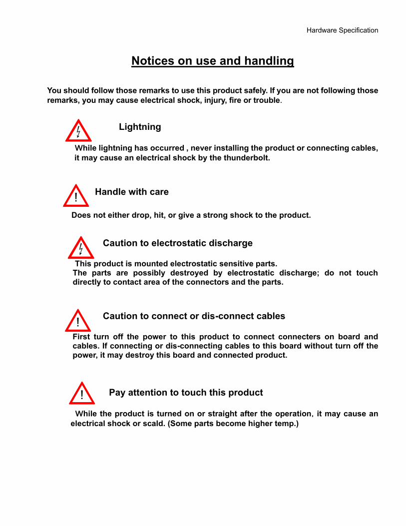
Notices on use and handling
You should follow those remarks to use this product safely. If you are not following those
remarks, you may cause electrical shock, injury, fire or trouble.
Lightning While lightning has occurred , never installing the product or connecting cables,
it may cause an electrical shock by the thunderbolt.
Handle with care
Does not either drop, hit, or give a strong shock to the product.
Caution to electrostatic discharge
This product is mounted electrostatic sensitive parts. The parts are possibly destroyed by electrostatic discharge; do not touch directly to contact area of the connectors and the parts.
Caution to connect or dis-connect cables
First turn off the power to this product to connect connecters on board and cables. If connecting or dis-connecting cables to this board without turn off the power, it may destroy this board and connected product.
Pay attention to touch this product
While the product is turned on or straight after the operation,it may cause an
electrical shock or scald. (Some parts become higher temp.)
!
!
!
Hardware Specification
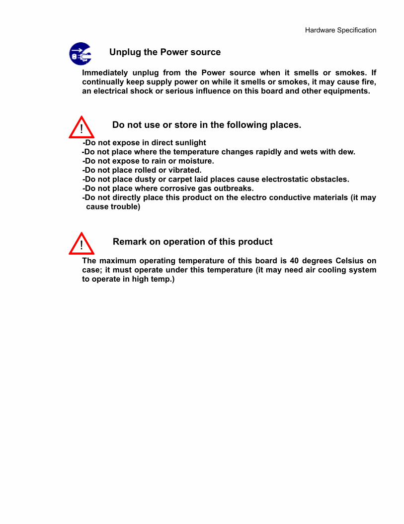
Unplug the Power source
Immediately unplug from the Power source when it smells or smokes. If continually keep supply power on while it smells or smokes, it may cause fire, an electrical shock or serious influence on this board and other equipments.
Do not use or store in the following places.
-Do not expose in direct sunlight -Do not place where the temperature changes rapidly and wets with dew.
-Do not expose to rain or moisture. -Do not place rolled or vibrated. -Do not place dusty or carpet laid places cause electrostatic obstacles. -Do not place where corrosive gas outbreaks. -Do not directly place this product on the electro conductive materials (it may cause trouble)
Remark on operation of this product
The maximum operating temperature of this board is 40 degrees Celsius on case; it must operate under this temperature (it may need air cooling system to operate in high temp.)
!
!
Hardware Specification
Revision history
Revision Release date Revised contents Remarks Rev1.00 Rev1.01 Rev1.02 Rev1.03 Rev1.04 Rev1.05
2018/10/02 2018/11/07 2019/02/21 2019/02/25 2019/02/27 2019/06/21
Release
Amend 5.7 LED Amend 5.13 LAN Amend 2. Specification list Amend 5.13 LAN Amend 5.10 Micro SD Card diagram, Add Comment Add 6. Signal Name
Hardware Specification
Content
1. OVERVIEW ............................................................................................................................................... 1
2. BOARD SPECIFICATIONS ...................................................................................................................... 1
3. BOARD ..................................................................................................................................................... 2
3.1. BOARD SIZE ..................................................................................................................................... 2 3.2. EXTERNAL VIEW.............................................................................................................................. 3
4. BLOCK DIAGRAM ................................................................................................................................... 4
5. FUNCTIONS ............................................................................................................................................. 5
5.1. POWER.............................................................................................................................................. 5 5.2. RESET AND JTAG ............................................................................................................................ 6 5.3. CLOCK .............................................................................................................................................. 7 5.4. SERIAL FLASH ROM ........................................................................................................................ 7 5.5. MIPI .................................................................................................................................................... 8 5.6. WIFI .................................................................................................................................................... 8 5.7. LED .................................................................................................................................................... 9 5.8. PUSH SW .......................................................................................................................................... 9 5.9. USB .................................................................................................................................................. 10 5.10. MICRO SD CARD .............................................................................................................................. 11 5.11. EEPROM.......................................................................................................................................... 11 5.12. SDRAM ............................................................................................................................................ 12 5.13. LAN .................................................................................................................................................. 13 5.14. EXTEND PIN HEADER ................................................................................................................... 14
5.14.1. CN2 ........................................................................................................................................... 14 5.14.2. CN3 ........................................................................................................................................... 14 5.14.3. CN4 and CN10 ......................................................................................................................... 15 5.14.4. CN8 ........................................................................................................................................... 15
6. CONNECTORS ....................................................................................................................................... 16
6.1. CONNECTOR LIST ......................................................................................................................... 16 6.1.1. CN1 ........................................................................................................................................... 16 6.1.2. CN2 ........................................................................................................................................... 17 6.1.3. CN3 ........................................................................................................................................... 17 6.1.4. CN4 ........................................................................................................................................... 18 6.1.5. CN5 ........................................................................................................................................... 18 6.1.6. CN6 ........................................................................................................................................... 19 6.1.7. CN7 ........................................................................................................................................... 19 6.1.8. CN8 ........................................................................................................................................... 20 6.1.9. CN9 ........................................................................................................................................... 21 6.1.10. CN10 ......................................................................................................................................... 21 6.1.11. CN11 ......................................................................................................................................... 22 6.1.12. CN12 ......................................................................................................................................... 22 6.1.13. CN13 ......................................................................................................................................... 22 6.1.14. CN14 ......................................................................................................................................... 23 6.1.15. CN15 ......................................................................................................................................... 23
7. SWITCH .................................................................................................................................................. 24
7.1. SWITCH LIST .................................................................................................................................. 24
8. JUMPER PINS ........................................................................................................................................ 24
8.1. JUMPER LIST ................................................................................................................................. 24
1
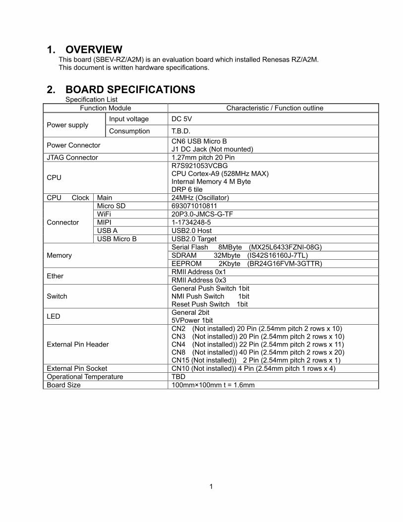
1. OVERVIEW This board (SBEV-RZ/A2M) is an evaluation board which installed Renesas RZ/A2M. This document is written hardware specifications.
2. BOARD SPECIFICATIONS Specification List
Function Module Characteristic / Function outline
Power supply Input voltage DC 5V
Consumption T.B.D.
Power Connector CN6 USB Micro B J1 DC Jack (Not mounted)
JTAG Connector 1.27mm pitch 20 Pin
CPU
R7S921053VCBG CPU Cortex-A9 (528MHz MAX) Internal Memory 4 M Byte DRP 6 tile
CPU Clock Main 24MHz (Oscillator)
Connector
Micro SD 693071010811
WiFi 20P3.0-JMCS-G-TF
MIPI 1-1734248-5
USB A USB2.0 Host
USB Micro B USB2.0 Target
Memory
Serial Flash 8MByte (MX25L6433FZNI-08G)
SDRAM 32Mbyte (IS42S16160J-7TL)
EEPROM 2Kbyte (BR24G16FVM-3GTTR)
Ether RMII Address 0x1
RMII Address 0x3
Switch General Push Switch 1bit NMI Push Switch 1bit Reset Push Switch 1bit
LED General 2bit 5VPower 1bit
External Pin Header
CN2 (Not installed) 20 Pin (2.54mm pitch 2 rows x 10) CN3 (Not installed)) 20 Pin (2.54mm pitch 2 rows x 10) CN4 (Not installed)) 22 Pin (2.54mm pitch 2 rows x 11) CN8 (Not installed)) 40 Pin (2.54mm pitch 2 rows x 20) CN15 (Not installed)) 2 Pin (2.54mm pitch 2 rows x 1)
External Pin Socket CN10 (Not installed)) 4 Pin (2.54mm pitch 1 rows x 4)
Operational Temperature TBD
Board Size 100mm×100mm t = 1.6mm
2
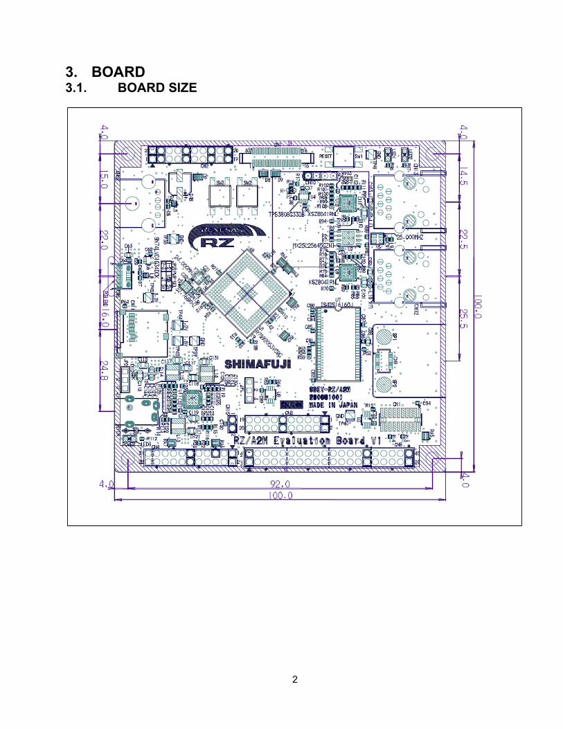
3. BOARD 3.1. BOARD SIZE
3
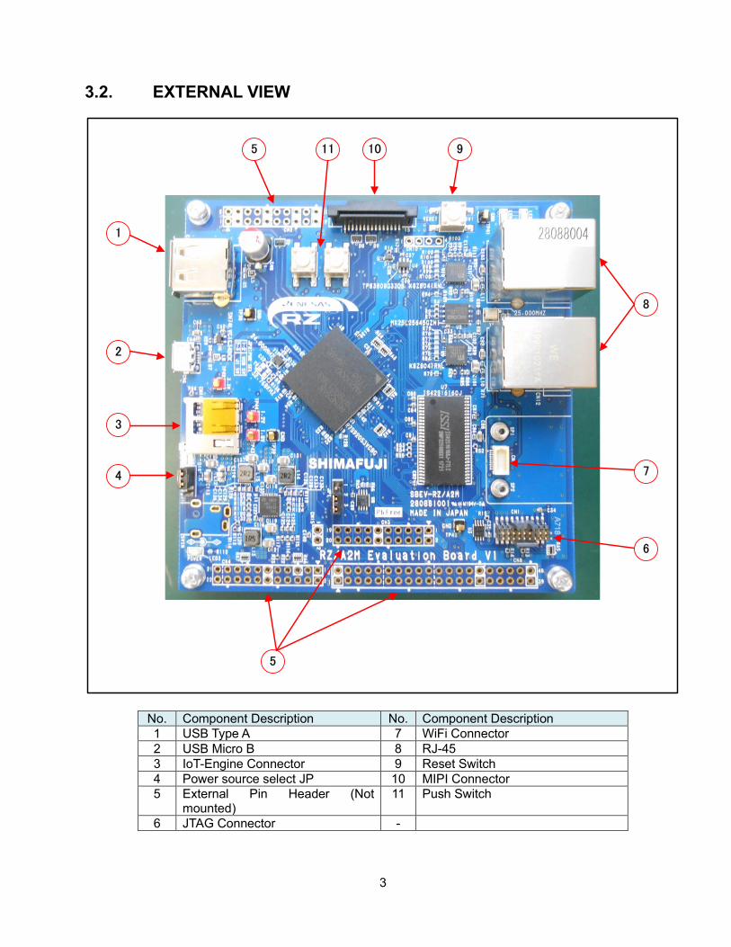
3.2. EXTERNAL VIEW
1
2
3
4
5
6
7
8
910115
No. Component Description No. Component Description
1 USB Type A 7 WiFi Connector
2 USB Micro B 8 RJ-45
3 IoT-Engine Connector 9 Reset Switch
4 Power source select JP 10 MIPI Connector
5 External Pin Header (Not mounted)
11 Push Switch
6 JTAG Connector -

4
4. BLOCK DIAGRAM This board block diagram.
RZ/A2M
PHYRMII
RMIIPHY
Ether NET I/F 2Port
ETHERC
24MHz EXTAL
DBGIFConnector
SYSTEMResetCircuit
Reset SW
USB
EEPROM
25MHzJTAG
Reset
CN12
CN13
CN1
SW1
RIIC0I2C
BSC
SDRAM32MByte
Connector
CN14
A1-A15D0-D15
QSPI0Serial Flash
8MByte
GPIO
DM1 micro SD
CN11
Connector
CN9
Pin Header
CN2
Pin Header
CN3
Pin Header
CN4
Pin Header
CN8
Pin Header
CN10
CSI-2
Connector
CN7
RIIC1/2
CSI
I2C
5V SwitchUSBType A
USB Micro B
CN5
CN6
JP2
DC Jack DCDC
3.3V
1.8V
1.2V
GPIO
LED
Push Switch
Clock

5
5. FUNCTIONS 5.1. POWER
This board has a power input connector USB Micro B (CN6) and DC jack (J1) to supply DC power. The DC-DC convertor on this board generate the several power which used on this board and the LED 3 illuminate when power is supplied.
Note : A DC jack is not mounted at factory. - Input Voltage : DC 5V (+5%, -5%) , Max Current : T.B.D. Power supply structure
D5VDC/DC 5V->3.3V
DC/DC 5V->1.8V
DC/DC 5V->1.2V
D3.3V
D1.8V
USB Power 5VIN
J1(Not mounted)
JP2U11
D1.2V
VBUS_5VD3.3V D1.8V D1.2V
AC adapter Power DC 5VIN
LED3
CN15(Not mounted)D5V
5V Out Pin Header
USB Micro
CN6
The recommended plug and jack
+-
Center +5VGND
PLUG TYPE : Outer Diameter φ4㎜ x Inner Diameter φ1.7㎜ (Voltage classification:EIAJ2)
Polarity:Center(+)
DC Jack PART NO.: M04-730A0 (Marushin musen)
6
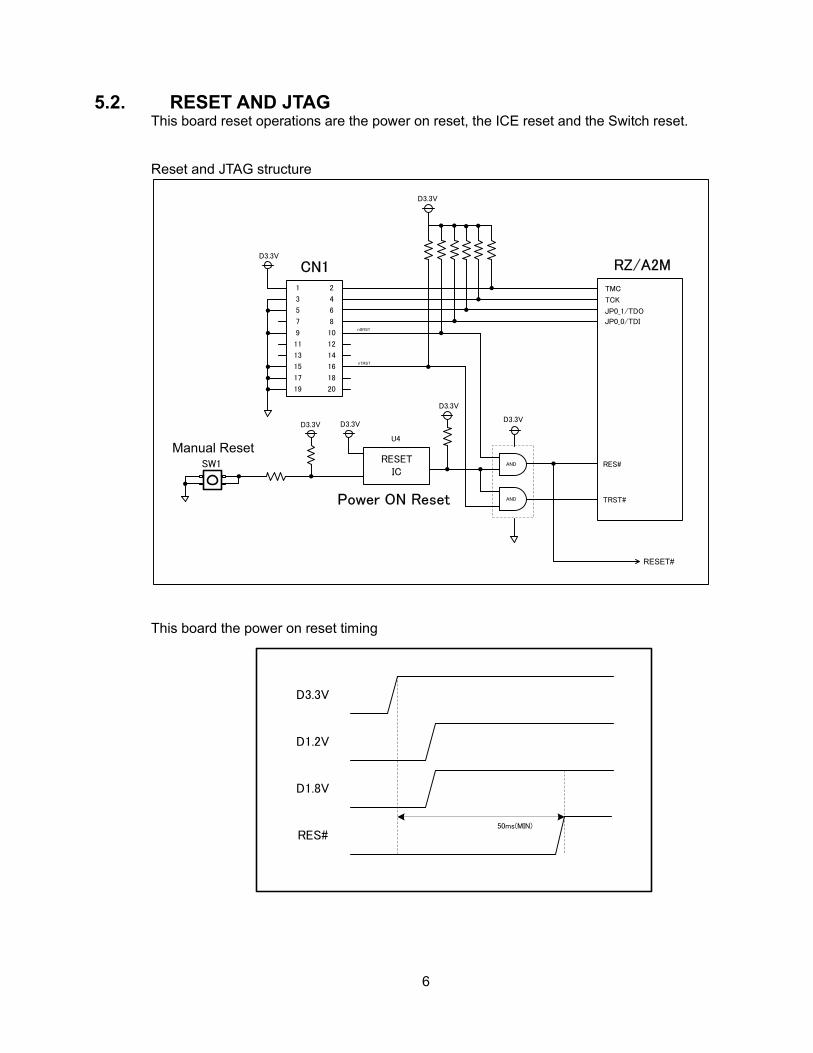
5.2. RESET AND JTAG This board reset operations are the power on reset, the ICE reset and the Switch reset. Reset and JTAG structure
Manual ResetSW1
D3.3V
RESETIC
D3.3V
AND
D3.3V
AND
D3.3V
nTRST
nSRST
RZ/A2M
TRST#
RES#
RESET#
3
1
7
5
9
13
11
17
15
19
4
2
8
6
10
14
12
18
16
20
D3.3V
TMC
TCK
JP0_1/TDO
JP0_0/TDI
D3.3V
Power ON Reset
U4
CN1
This board the power on reset timing
D3.3V
50ms(MIN)
D1.2V
D1.8V
RES#
7
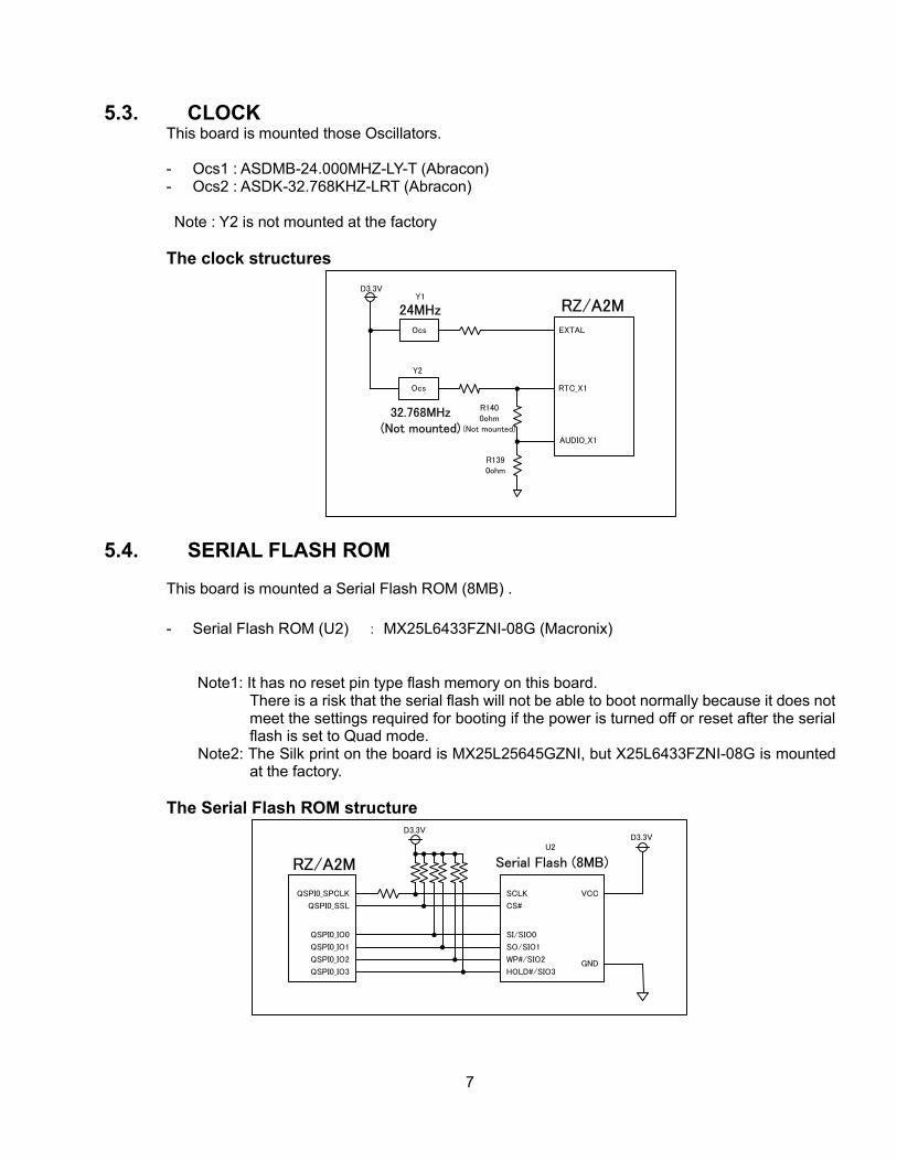
5.3. CLOCK This board is mounted those Oscillators. - Ocs1 : ASDMB-24.000MHZ-LY-T (Abracon) - Ocs2 : ASDK-32.768KHZ-LRT (Abracon) Note : Y2 is not mounted at the factory
The clock structures
Ocs
24MHz
D3.3VY1
RZ/A2MEXTAL
RTC_X1Ocs
32.768MHz(Not mounted)
Y2
AUDIO_X1
R1400ohm
(Not mounted)
R1390ohm
5.4. SERIAL FLASH ROM This board is mounted a Serial Flash ROM (8MB) .
- Serial Flash ROM (U2) : MX25L6433FZNI-08G (Macronix)
Note1: It has no reset pin type flash memory on this board.
There is a risk that the serial flash will not be able to boot normally because it does not meet the settings required for booting if the power is turned off or reset after the serial flash is set to Quad mode.
Note2: The Silk print on the board is MX25L25645GZNI, but X25L6433FZNI-08G is mounted at the factory.
The Serial Flash ROM structure
RZ/A2M
QSPI0_SSL
QSPI0_IO1
QSPI0_IO2
QSPI0_IO0
QSPI0_SPCLK
QSPI0_IO3
D3.3V
SCLK
SI/SIO0
CS#
SO/SIO1
WP#/SIO2
HOLD#/SIO3
VCC
GND
Serial Flash (8MB)U2
D3.3V

8
5.5. MIPI This board is mounted an FFC connector for MIPI CSI-2 I/F.
A 1mm pitch flexible cable can be inserted.
- MIPI Connector (CN7) : 1-1734248-5 (TE)
The MIPI connector structure
3.3V
RZ/A2M
CSI_DATA0P
CSI_DATA1P
CSI_CLKN
CSI_DATA1N
CSI_DATA0N
CSI_CLKP
3.3V
2
GND
CN71-1734248-5
PD_3/RIIC1SDA
PD_4/RIIC2SCL
PD_2/RIIC1SCL
PD_5/RIIC2SDA
1
3
4
5
6
7
8
9
10
11
12
13
14
15
GND
GND
GND
VCC
5.6. WiFi This board is mounted a connector for IoT-Engine WiFi ESP32 (SEMB1401-1).
Attention: The IO input / output settings when connect extension board.
- WiFi ESP32 Connector (CN9) : 20P3.0-JMCS-G-TF(JST)
- Compatible connector : 20R-JMCS-G-TF(JST)
The WiFi connector structure
3
1
7
5
9
13
11
17
15
19
4
2
8
6
10
14
12
18
16
20
RZ/A2M
PH_0/IRQ3
D3.3V
PJ_1/RXD1
PG_4/RSPCK1
PJ_7
PJ_4/CTS#1
PG_5/MOSI1
PH_1/IRQ2
PG_7/SSL10
PG_6/MISO1
PJ_3/RTS#1
RZ/A2MCN9
PJ_2/TXD1
R42(Not mounted)
3.3V3.3V
9
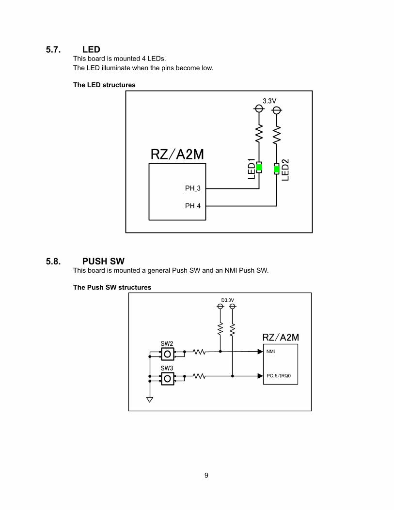
5.7. LED This board is mounted 4 LEDs.
The LED illuminate when the pins become low.
The LED structures
RZ/A2M
PH_3
PH_4
3.3V
LED
1
LED
2
5.8. PUSH SW This board is mounted a general Push SW and an NMI Push SW.
The Push SW structures
RZ/A2MNMI
PC_5/IRQ0
D3.3V
SW2
SW3
10
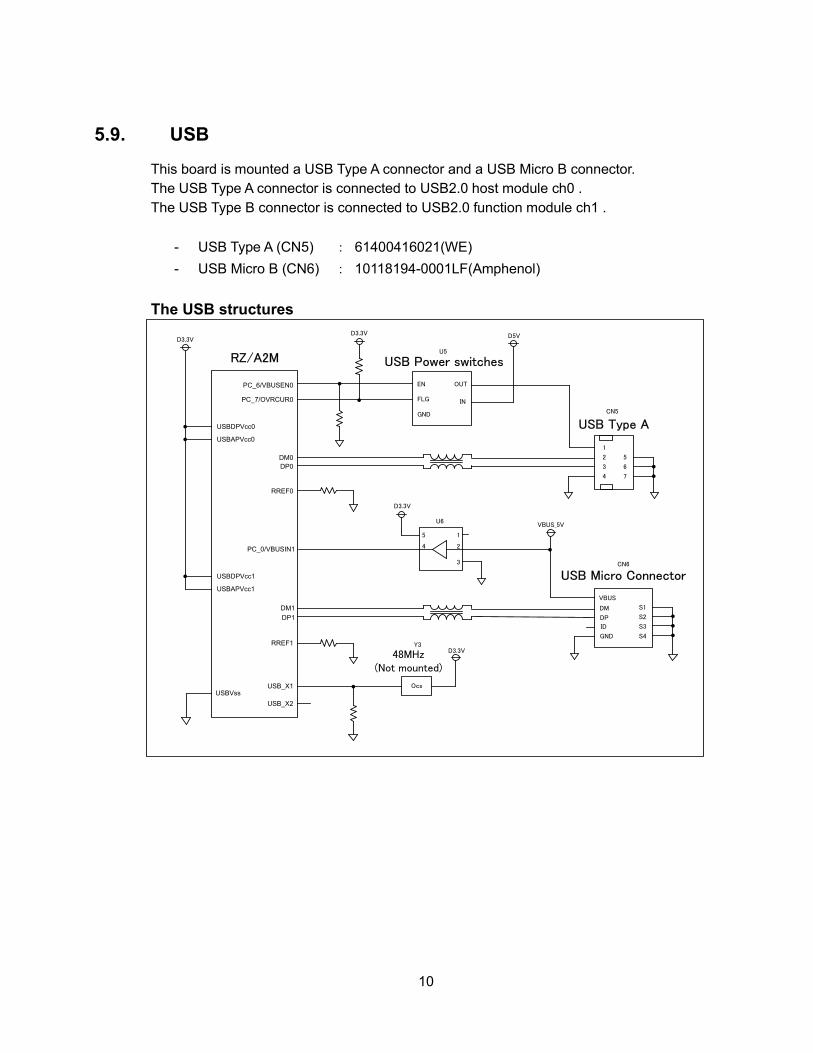
5.9. USB This board is mounted a USB Type A connector and a USB Micro B connector.
The USB Type A connector is connected to USB2.0 host module ch0 .
The USB Type B connector is connected to USB2.0 function module ch1 .
- USB Type A (CN5) : 61400416021(WE)
- USB Micro B (CN6) : 10118194-0001LF(Amphenol)
The USB structures
RZ/A2M
DP0
DM0
USB_X1
RREF0
DM1
DP1
USB_X2
RREF1
PC_7/OVRCUR0
PC_6/VBUSEN0 EN
FLG
USB Power switchesU5
OUT
IN
D5V
GND
D3.3V
2
1
4
3
5
7
6
USB Type ACN5
DM
VBUS
ID
DP
S1
S3
S2
USB Micro ConnectorCN6
VBUS_5V
GND S4
5
4
U6
1
2
3
PC_0/VBUSIN1
D3.3V
USBVss
USBDPVcc0
USBAPVcc0
USBDPVcc1
USBAPVcc1
D3.3V
Ocs
Y3D3.3V48MHz
(Not mounted)
11
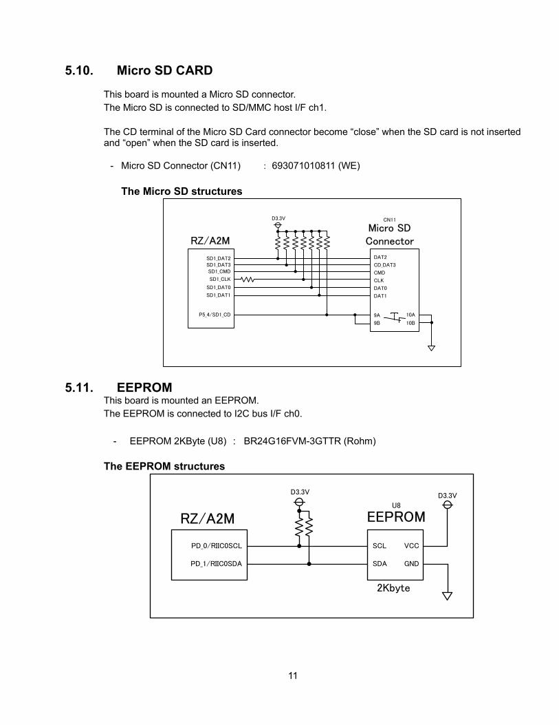
5.10. Micro SD CARD This board is mounted a Micro SD connector.
The Micro SD is connected to SD/MMC host I/F ch1.
The CD terminal of the Micro SD Card connector become “close” when the SD card is not inserted and “open” when the SD card is inserted.
- Micro SD Connector (CN11) : 693071010811 (WE)
The Micro SD structures
SD1_DAT2 SD1_DAT3
SD1_CMD
SD1_DAT0
SD1_DAT1
P5_4/SD1_CD
D3.3V
SD1_CLK
Micro SD Connector
CN11
DAT2
CD_DAT3
CMD
CLK
DAT0
DAT1
9A
9B
10A
10B
RZ/A2M
5.11. EEPROM This board is mounted an EEPROM.
The EEPROM is connected to I2C bus I/F ch0.
- EEPROM 2KByte (U8) : BR24G16FVM-3GTTR (Rohm)
The EEPROM structures
PD_0/RIIC0SCL
RZ/A2M
SCL
SDA
D3.3V
PD_1/RIIC0SDA
EEPROMU8
VCC
GND
D3.3V
2Kbyte
12
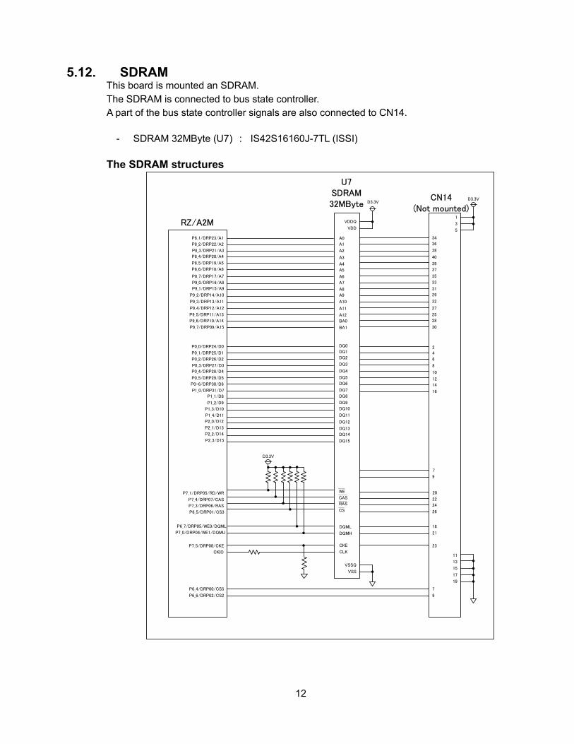
5.12. SDRAM This board is mounted an SDRAM.
The SDRAM is connected to bus state controller.
A part of the bus state controller signals are also connected to CN14.
- SDRAM 32MByte (U7) : IS42S16160J-7TL (ISSI)
The SDRAM structures
RZ/A2M
P9_7/DRP09/A15
U7SDRAM 32MByte
BA1
BA0
A12
A11
A10
A9
A8
A7
A6
A5
A4
A3
A2
A1
A0
CS
RAS
CAS
WE
DQMH
DQML
CKE
CLK
P9_6/DRP10/A14
P9_5/DRP11/A13
P9_4/DRP12/A12
P9_3/DRP13/A11
P9_2/DRP14/A10
P9_1/DRP15/A9
P9_0/DRP16/A8
P8_7/DRP17/A7
P8_6/DRP18/A6
P8_5/DRP19/A5
P8_4/DRP20/A4
P8_3/DRP21/A3
P8_2/DRP22/A2
P8_1/DRP23/A1
P6_5/DRP01/CS3
P7_3/DRP06/RAS
P7_4/DRP07/CAS
P7_1/DRP05/RD/WR
P7_0/DRP04/WE1/DQMU
P6_7/DRP05/WE0/DQML
P7_5/DRP08/CKE
CKIO
D3.3V
VDDQ
VDD
VSSQ
VSS
D3.3V
DQ15
DQ14
DQ13
DQ12
DQ11
DQ10
DQ9
DQ8
DQ7
DQ6
DQ5
DQ4
DQ3
DQ2
DQ1
DQ0
P2_3/D15
P2_2/D14
P2_1/D13
P2_0/D12
P1_4/D11
P1_3/D10
P1_2/D9
P1_1/D8
P1_0/DRP31/D7
P0-6/DRP30/D6
P0_5/DRP29/D5
P0_4/DRP28/D4
P0_3/DRP27/D3
P0_2/DRP26/D2
P0_1/DRP25/D1
P0_0/DRP24/D0
CN14(Not mounted)
P6_4/DRP00/CS5
P6_6/DRP02/CS2
11
13
15
17
19
30
28
25
27
32
29
31
33
35
37
39
40
38
36
34
16
14
12
10
8
6
4
2
26
24
22
20
21
18
23
9
7
7
9
1
3
D3.3V
5
13
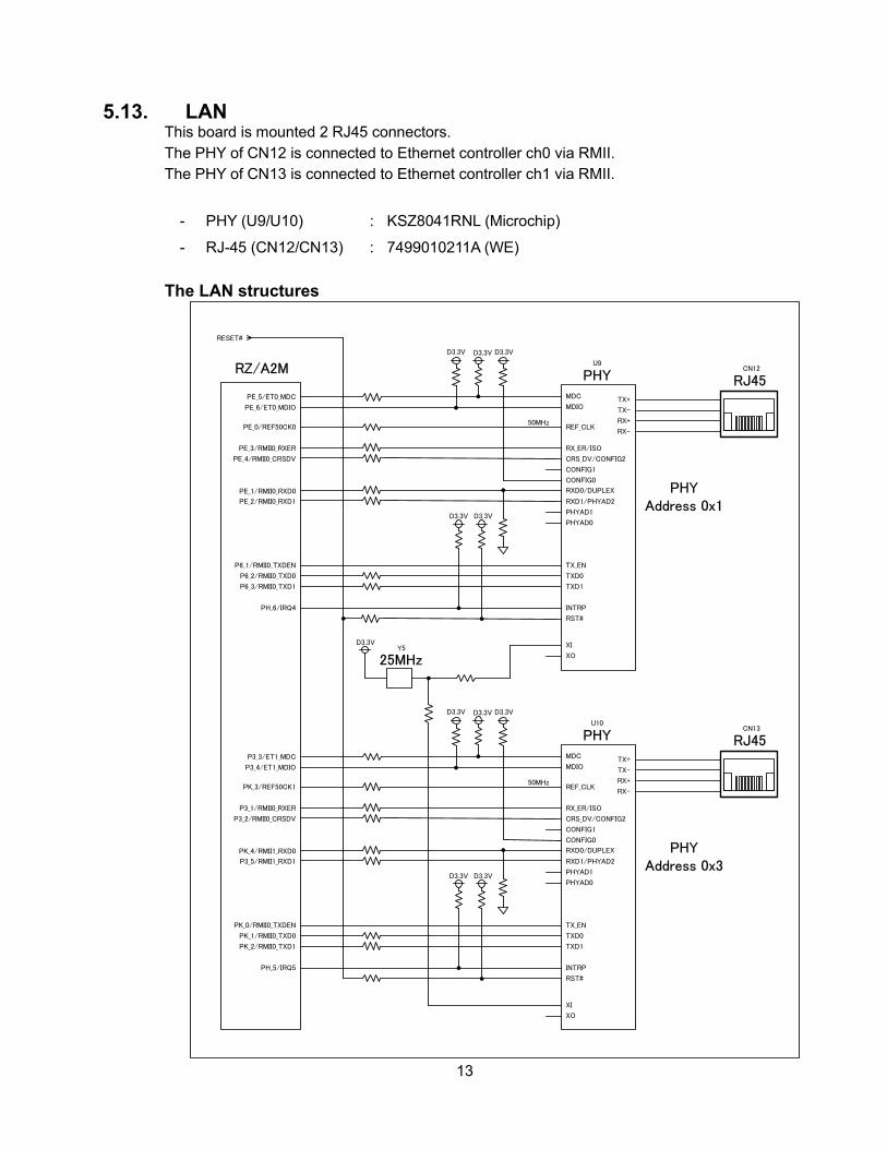
5.13. LAN This board is mounted 2 RJ45 connectors.
The PHY of CN12 is connected to Ethernet controller ch0 via RMII.
The PHY of CN13 is connected to Ethernet controller ch1 via RMII.
- PHY (U9/U10) : KSZ8041RNL (Microchip)
- RJ-45 (CN12/CN13) : 7499010211A (WE)
The LAN structures
PE_0/REF50CK0
PE_3/RMII0_RXER
PE_4/RMII0_CRSDV
PE_2/RMII0_RXD1
P6_1/RMII0_TXDEN
P6_2/RMII0_TXD0
P6_3/RMII0_TXD1
PH_6/IRQ4
PHY
PE_6/ET0_MDIO
PE_5/ET0_MDC MDC
MDIO
REF_CLK
RX_ER/ISO
CRS_DV/CONFIG2
CONFIG1
CONFIG0
RXD1/PHYAD2
PHYAD1
PHYAD0
TX_EN
TXD0
TXD1
INTRP
XI
XO
RJ45TX+
TX-
RX+
RX-
RESET#
PHYAddress 0x1
CN12
50MHz
PE_1/RMII0_RXD0 RXD0/DUPLEX
RST#
U9
D3.3V D3.3V
D3.3V
D3.3V
D3.3V
25MHz
D3.3VY5
PHYMDC
MDIO
REF_CLK
RX_ER/ISO
CRS_DV/CONFIG2
CONFIG1
CONFIG0
RXD1/PHYAD2
PHYAD1
PHYAD0
TX_EN
TXD0
TXD1
INTRP
XI
XO
RJ45TX+
TX-
RX+
RX-
PHYAddress 0x3
CN13
50MHz
RXD0/DUPLEX
RST#
U10
D3.3V D3.3V
D3.3V
D3.3V
D3.3V
PK_3/REF50CK1
P3_1/RMII0_RXER
P3_2/RMII0_CRSDV
P3_5/RMII1_RXD1
PK_0/RMII0_TXDEN
PK_1/RMII0_TXD0
PK_2/RMII0_TXD1
PH_5/IRQ5
P3_4/ET1_MDIO
P3_3/ET1_MDC
PK_4/RMII1_RXD0
RZ/A2M

14
5.14. EXTEND PIN HEADER This board has through hole for 5 external pin headers.
It can extend when mount the pin header.
5.14.1. CN2 The CN2 structures
3
1
7
5
9
13
11
17
15
19
4
2
8
6
10
14
12
18
16
20
RZ/A2M
P4_4/TXOUT2P
D3.3V
P4_5/TXOUT2M
P4_0/TXOUT0P
P4_1/TXOUT0M
R20
CN2(Not mounted)
D3.3V
P4_6/TXCLKOUTP
D3.3V
P4_7/TXCLKOUTM
P4_2/TXOUT1P
P4_3/TXOUT1M
R21(Not Mounted)
D3.3V
RZ/A2M
R18(Not Mounted) R19
5.14.2. CN3 The CN3 structures
3
1
7
5
9
13
11
17
15
19
4
2
8
6
10
14
12
18
16
20
RZ/A2M
PL_3/MD_BOOT1
D3.3V
PL_4/MD_BOOT0
PL_1/MD_CLK
PL_2/MD_BOOT2
PL_0/MD_CLKS
PJ_6
P5_5/AN005/IRQ1
P5_6/AN006
PG_3/SSL00
PG_1/MOSI0
P5_0/AN000
PJ_5
P5_1/AN001
P5_2/AN002/IRQ6
RZ/A2MCN3
(Not mounted)
PG_0/RSPCK0
D3.3V
PG_2/MISO0
D3.3V
15
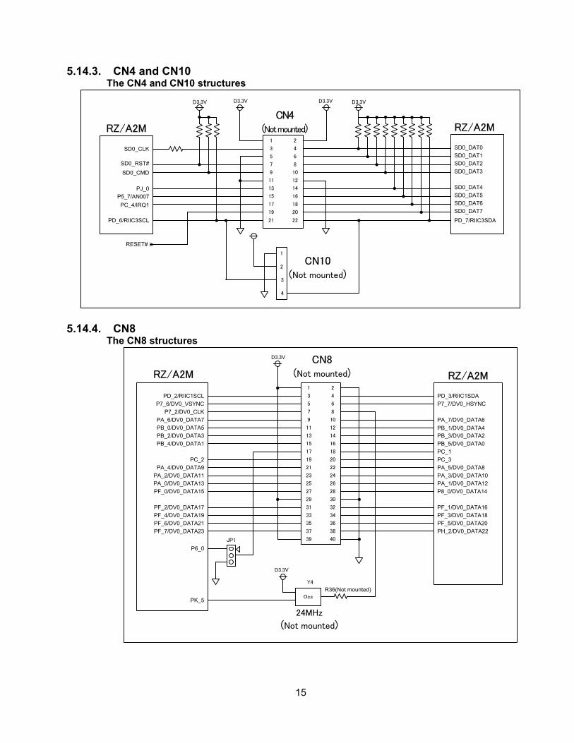
5.14.3. CN4 and CN10 The CN4 and CN10 structures
3
1
7
5
9
13
11
17
15
19
4
2
8
6
10
14
12
18
16
20
RZ/A2M
SD0_RST#
D3.3V
SD0_CLK
SD0_CMD
PJ_0
P5_7/AN007
PC_4/IRQ1
RESET#
SD0_DAT3
SD0_DAT1
SD0_DAT5
SD0_DAT4
SD0_DAT6
SD0_DAT7
RZ/A2MCN4
(Not mounted)
SD0_DAT0
D3.3V
SD0_DAT2
D3.3V D3.3V
21 22PD_6/RIIC3SCL PD_7/RIIC3SDA
1
2CN10
(Not mounted)3
4
5.14.4. CN8 The CN8 structures
3
1
7
5
9
13
11
17
15
19
23
21
25
27
31
29
33
35
39
37
4
2
8
6
10
14
12
18
16
20
22
24
26
28
32
30
34
36
40
38
RZ/A2M
P7_6/DV0_VSYNC
D3.3V
PD_2/RIIC1SCL
PA_6/DV0_DATA7
P7_2/DV0_CLK
PB_2/DV0_DATA3
PB_0/DV0_DATA5
PB_4/DV0_DATA1
PA_2/DV0_DATA11
PA_4/DV0_DATA9
PF_0/DV0_DATA15
PA_0/DV0_DATA13
PF_2/DV0_DATA17
PF_6/DV0_DATA21
PF_4/DV0_DATA19
PF_7/DV0_DATA23
PC_2
PA_7/DV0_DATA6
P7_7/DV0_HSYNC
PB_5/DV0_DATA0
PB_3/DV0_DATA2
PA_5/DV0_DATA8
PC_1
PA_3/DV0_DATA10
P8_0/DV0_DATA14
PF_1/DV0_DATA16
PF_3/DV0_DATA18
PF_5/DV0_DATA20
PH_2/DV0_DATA22
PC_3
PA_1/DV0_DATA12
RZ/A2M
PB_1/DV0_DATA4
CN8(Not mounted)
PD_3/RIIC1SDA
JP1
P6_0
Ocs
24MHz
(Not mounted)
Y4
D3.3V
PK_5
R36(Not mounted)
16
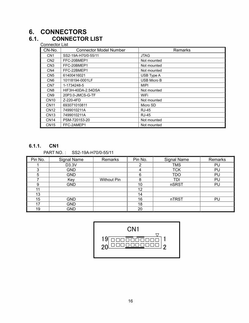
6. CONNECTORS 6.1. CONNECTOR LIST
Connector List
CN-No. Connector Model Number Remarks
CN1 SS2-19A-H70/0-55/11 JTAG
CN2 FFC-20BMEP1 Not mounted
CN3 FFC-20BMEP1 Not mounted
CN4 FFC-22BMEP1 Not mounted
CN5 61400416021 USB Type A
CN6 10118194-0001LF USB Micro B
CN7 1-1734248-5 MIPI
CN8 HIF3H-40DA-2.54DSA Not mounted
CN9 20P3.0-JMCS-G-TF WiFi
CN10 Z-220-4FD Not mounted
CN11 693071010811 Micro SD
CN12 7499010211A RJ-45
CN13 7499010211A RJ-45
CN14 PSM-720153-20 Not mounted
CN15 FFC-2AMEP1 Not mounted
6.1.1. CN1
PART NO.: SS2-19A-H70/0-55/11
Pin No. Signal Name Remarks Pin No. Signal Name Remarks
1 D3.3V 2 TMS PU
3 GND 4 TCK PU
5 GND 6 TDO PU
7 Key Without Pin 8 TDI PU
9 GND 10 nSRST PU
11 12
13 14
15 GND 16 nTRST PU
17 GND 18
19 GND 20
12
1920
CN1
17
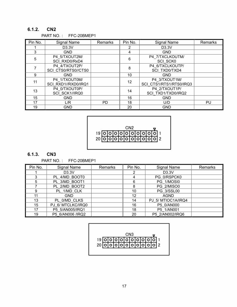
6.1.2. CN2
PART NO.: FFC-20BMEP1
Pin No. Signal Name Remarks Pin No. Signal Name Remarks
1 D3.3V 2 D3.3V
3 GND 4 GND
5 P4_5/TXOUT2M/ SCI_RXD0/RxD4
6
P4_7/TXCLKOUTM/ SCI_SCK0
7 P4_4/TXOUT2P/
SCI_CTS0/RTS0//CTS0
8 P4_6/TXCLKOUTP/
SCI_TXD0/TXD4
9 GND 10 GND
11 P4_1/TXOUT0M/
SCI_RXD1//RXD0/IRQ1
12 P4_3/TXOUT1M/
SCI_CTS1/RTS1/RTS0/IRQ3
13 P4_0/TXOUT0P/ SCI_SCK1//IRQ0
14
P4_2/TXOUT1P/ SCI_TXD1/TXD0/IRQ2
15 GND 16 GND
17 L/R PD 18 U/D PU
19 GND 20 GND
12
1920
CN2
6.1.3. CN3
PART NO.: FFC-20BMEP1
Pin No. Signal Name Remarks Pin No. Signal Name Remarks
1 D3.3V 2 D3.3V
3 PL_4/MD_BOOT0 4 PG_0/RSPCK0
5 PL_3/MD_BOOT1 6 PG_1/MOSI0
7 PL_2/MD_BOOT2 8 PG_2/MISO0
9 PL_1/MD_CLK 10 PG_3/SSL00
11 GND 12 AGND
13 PL_0/MD_CLKS 14 PJ_5/ MTIOC1A/IRQ4
15 PJ_6/ MTCLKC/IRQ0 16 P5_0/AN000
17 P5_5/AN005/IRQ1 18 P5_1/AN001
19 P5_6/AN006 /IRQ2 20 P5_2/AN002/IRQ6
12
1920
CN3

18
6.1.4. CN4
PART NO.: FFC-22BMEP1
Pin No. Signal Name Remarks Pin No. Signal Name Remarks
1 D3.3V 2 D3.3V
3 SD0_CLK 4 SD0_DAT0 PU
5 GND 6 SD0_DAT1 PU
7 SD0_RST# PU 8 SD0_DAT2 PU
9 SD0_CMD PU 10 SD0_DAT3 PU
11 GND 12 GND
13 PJ_0/ SCK1 14 SD0_DAT4 PU
15 P5_7/AN007 /IRQ3 16 SD0_DAT5 PU
17 PC_4/IRQ1 18 SD0_DAT6 PU
19 RESET# 20 SD0_DAT7 PU
21 PD_6/RIIC3SCL PU
Share with CN10-3
22 PD_7/RIIC3SDA PU
Share with CN10-4
12
2122
CN4
6.1.5. CN5
PART NO.: 61400416021
Pin No. Signal Name Remarks
1 D5.0V
2 DM0
3 DP0
4 GND
19
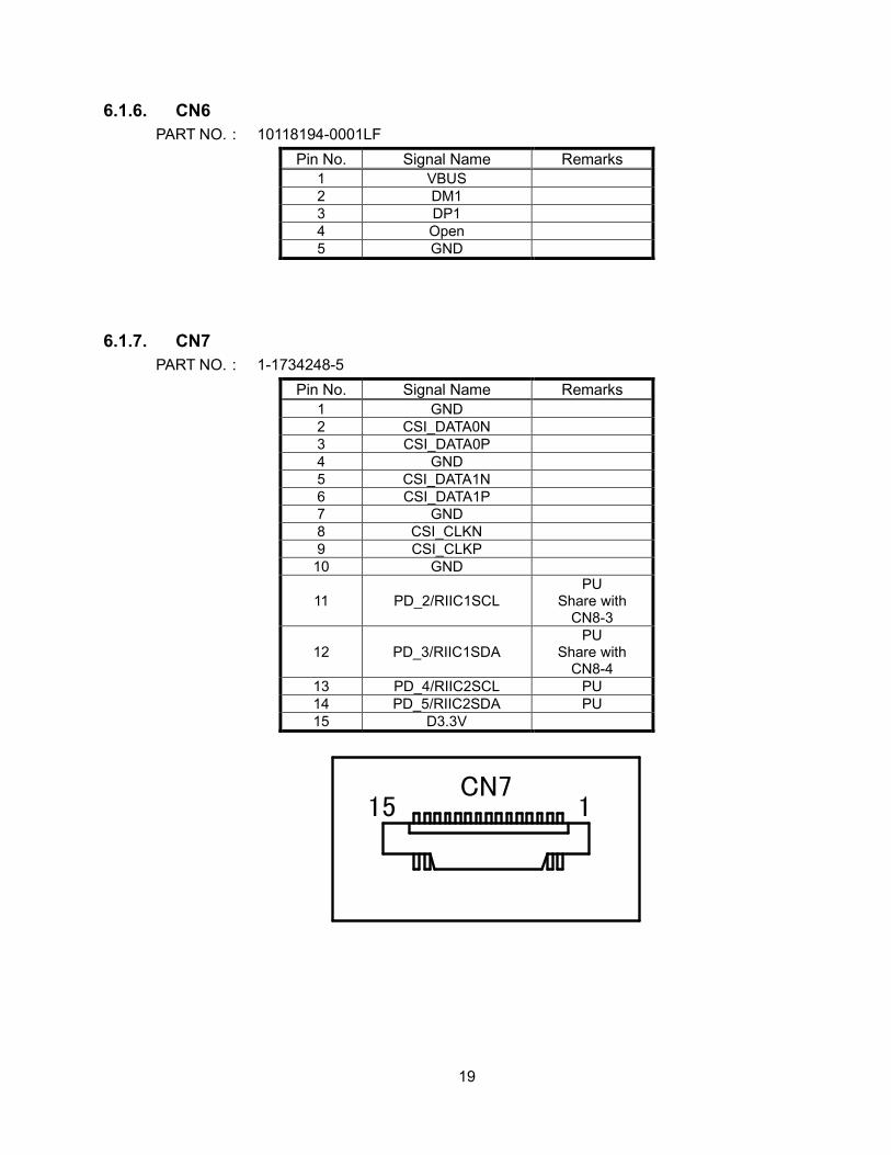
6.1.6. CN6
PART NO.: 10118194-0001LF
Pin No. Signal Name Remarks
1 VBUS
2 DM1
3 DP1
4 Open
5 GND
6.1.7. CN7
PART NO.: 1-1734248-5
Pin No. Signal Name Remarks
1 GND
2 CSI_DATA0N
3 CSI_DATA0P
4 GND
5 CSI_DATA1N
6 CSI_DATA1P
7 GND
8 CSI_CLKN
9 CSI_CLKP
10 GND
11 PD_2/RIIC1SCL PU
Share with CN8-3
12 PD_3/RIIC1SDA PU
Share with CN8-4
13 PD_4/RIIC2SCL PU
14 PD_5/RIIC2SDA PU
15 D3.3V
CN7115
20
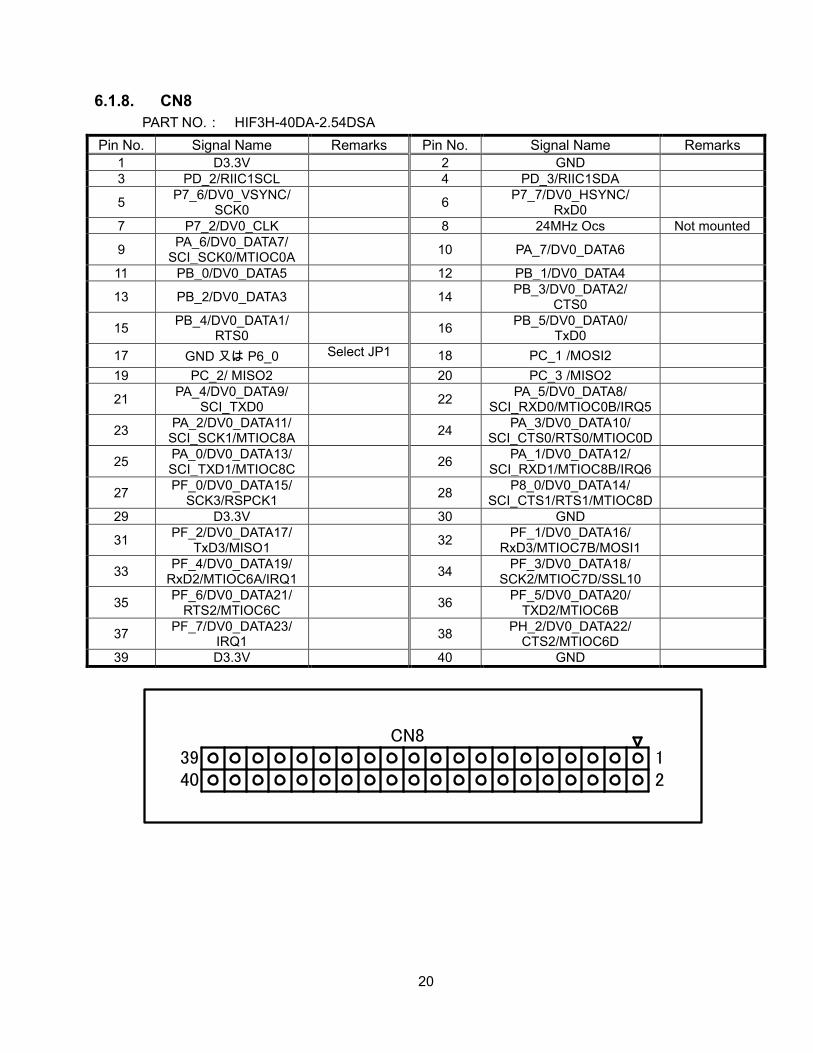
6.1.8. CN8
PART NO.: HIF3H-40DA-2.54DSA
Pin No. Signal Name Remarks Pin No. Signal Name Remarks
1 D3.3V 2 GND
3 PD_2/RIIC1SCL 4 PD_3/RIIC1SDA
5 P7_6/DV0_VSYNC/
SCK0
6 P7_7/DV0_HSYNC/
RxD0
7 P7_2/DV0_CLK 8 24MHz Ocs Not mounted
9 PA_6/DV0_DATA7/
SCI_SCK0/MTIOC0A
10 PA_7/DV0_DATA6
11 PB_0/DV0_DATA5 12 PB_1/DV0_DATA4
13 PB_2/DV0_DATA3
14 PB_3/DV0_DATA2/
CTS0
15 PB_4/DV0_DATA1/
RTS0
16 PB_5/DV0_DATA0/
TxD0
17 GND 又は P6_0 Select JP1 18 PC_1 /MOSI2
19 PC_2/ MISO2 20 PC_3 /MISO2
21 PA_4/DV0_DATA9/
SCI_TXD0
22 PA_5/DV0_DATA8/
SCI_RXD0/MTIOC0B/IRQ5
23 PA_2/DV0_DATA11/
SCI_SCK1/MTIOC8A
24 PA_3/DV0_DATA10/
SCI_CTS0/RTS0/MTIOC0D
25 PA_0/DV0_DATA13/ SCI_TXD1/MTIOC8C
26
PA_1/DV0_DATA12/ SCI_RXD1/MTIOC8B/IRQ6
27 PF_0/DV0_DATA15/
SCK3/RSPCK1
28 P8_0/DV0_DATA14/
SCI_CTS1/RTS1/MTIOC8D
29 D3.3V 30 GND
31 PF_2/DV0_DATA17/
TxD3/MISO1
32 PF_1/DV0_DATA16/
RxD3/MTIOC7B/MOSI1
33 PF_4/DV0_DATA19/
RxD2/MTIOC6A/IRQ1
34 PF_3/DV0_DATA18/
SCK2/MTIOC7D/SSL10
35 PF_6/DV0_DATA21/
RTS2/MTIOC6C
36 PF_5/DV0_DATA20/
TXD2/MTIOC6B
37 PF_7/DV0_DATA23/
IRQ1
38 PH_2/DV0_DATA22/
CTS2/MTIOC6D
39 D3.3V 40 GND
12
3940
CN8
21
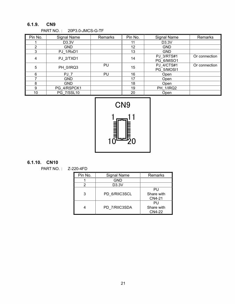
6.1.9. CN9
PART NO.: 20P3.0-JMCS-G-TF
Pin No. Signal Name Remarks Pin No. Signal Name Remarks
1 D3.3V 11 D3.3V
2 GND 12 GND
3 PJ_1/RxD1 13 GND
4 PJ_2/TXD1
14 PJ_3/RTS#1 PG_6/MISO1
Or connection
5 PH_0/IRQ3 PU
15 PJ_4/CTS#1 PG_5/MOSI1
Or connection
6 PJ_7 PU 16 Open
7 GND 17 Open
8 GND 18 Open
9 PG_4/RSPCK1 19 PH_1/IRQ2
10 PG_7/SSL10 20 Open
1 11
2010
CN9
6.1.10. CN10
PART NO.: Z-220-4FD
Pin No. Signal Name Remarks
1 GND
2 D3.3V
3 PD_6/RIIC3SCL PU
Share with CN4-21
4 PD_7/RIIC3SDA PU
Share with CN4-22

22
6.1.11. CN11
PART NO.: 693071010811
Pin No. Signal Name Remarks
1 SD1_DAT2 PU
2 SD1_DAT3 PU
3 SD1_CMD PU
4 D3.3V
5 SD1_CLK PU
6 GND
7 SD1_DAT0 PU
8 SD1_DAT1 PU
9A/B P5_4/SD1_CD PU
6.1.12. CN12
PART NO.: 7499010211A
Pin No. Signal Name Remarks
1 TX+
2 TX-
3 RX+
4 NC
5 NC
6 RX-
7 NC
8 NC
6.1.13. CN13
PART NO.: 7499010211A
Pin No. Signal Name Remarks
1 TX+
2 TX-
3 RX+
4 NC
5 NC
6 RX-
7 NC
8 NC
23
6.1.14. CN14
PART NO.: PSM-720153-20
Pin No. Signal Name Remarks Pin No. Signal Name Remarks
1 D3.3V 2 P0_0/DRP24/D0 Share with U7
3 D3.3V 4 P0_1/DRP25/D1 Share with U7
5 D3.3V 6 P0_2/DRP26/D2 Share with U7
7 P6_4/DRP00/CS5 Share with U7 8 P0_3/DRP27/D3 Share with U7
9 P6_6/DRP02/CS2 Share with U7 8 P0_4/DRP28/D4 Share with U7
11 GND 12 P0_5/DRP29/D5 Share with U7
13 GND 14 P0_6/DRP30/D6 Share with U7
15 GND 16 P1_0/DRP31/D7 Share with U7
17 GND 18 P6_7/DRP03/WE0/DQML Share with U7
19 GND 20 P7_1/DRP05/RD/WR Share with U7
21 P7_0/DRP04/WE1/DQMU Share with U7 22 P7_4/DRP07/CAS Share with U7
23 P7_5/DRP08/CKE Share with U7 24 P7_3/DRP06/RAS Share with U7
25 P9_5/DRP11/A13 Share with U7 26 P6_5/DRP01/CS3 Share with U7
27 P9_4/DRP12/A12 Share with U7 28 P9_6/DRP10/A14 Share with U7
29 P9_2/DRP14/A10 Share with U7 30 P9_7/DRP09/A15 Share with U7
31 P9_1/DRP15/A9 Share with U7 32 P9_3/DRP13/A11 Share with U7
33 P9_0/DRP16/A8 Share with U7 34 P8_1/DRP23/A1 Share with U7
35 P8_7/DRP17/A7 Share with U7 36 P8_2/DRP22/A2 Share with U7
37 P8_6/DRP18/A6 Share with U7 38 P8_3/DRP21/A3 Share with U7
39 P8_5/DRP19/A5 Share with U7 40 P8_4/DRP20/A4 Share with U7
6.1.15. CN15
PART NO.: FFC-2AMEP1
Pin No. Signal Name Remarks
1 D5V
2 GND
24
7. SWITCH 7.1. SWITCH LIST
Switch List
CN-NO. Switch model No. Remarks
SW1 2-1437565-9 Reset
SW2 2-1437565-9 NMI
SW3 2-1437565-9 General I/O
8. JUMPER PINS 8.1. JUMPER LIST
Jumper List
CN-NO. Jumper pin model No. Remarks
JP1 XJ8D-0311 Signal switch
JP2 XJ8D-0311 Input power connector select
Related Documents


![1.05 Mb [Download]](https://static.cupdf.com/doc/110x72/587f2c131a28abb43f8bc435/105-mb-download.jpg)

