Engr. Rashid Farid Chishti Lecturer, Faculty of Engineering & Technology International Islamic university Islamabad. Mobile: 0321 5300 497 E-mail: [email protected] 3/20/22 www.iiu.edu.pk 1 DESIGN AND IMPLEMENTATION OF SIMPLE AS POSSIBLE COMPUTER (SAP-1)

Welcome message from author
This document is posted to help you gain knowledge. Please leave a comment to let me know what you think about it! Share it to your friends and learn new things together.
Transcript

Saturday, April 15, 2023www.iiu.edu.pk
1
Engr. Rashid Farid ChishtiLecturer, Faculty of Engineering & Technology
International Islamic university Islamabad.Mobile: 0321 5300 497
E-mail: [email protected]
DESIGN AND IMPLEMENTATION OF SIMPLE AS POSSIBLE COMPUTER
(SAP-1)

Saturday, April 15, 2023www.iiu.edu.pk
2
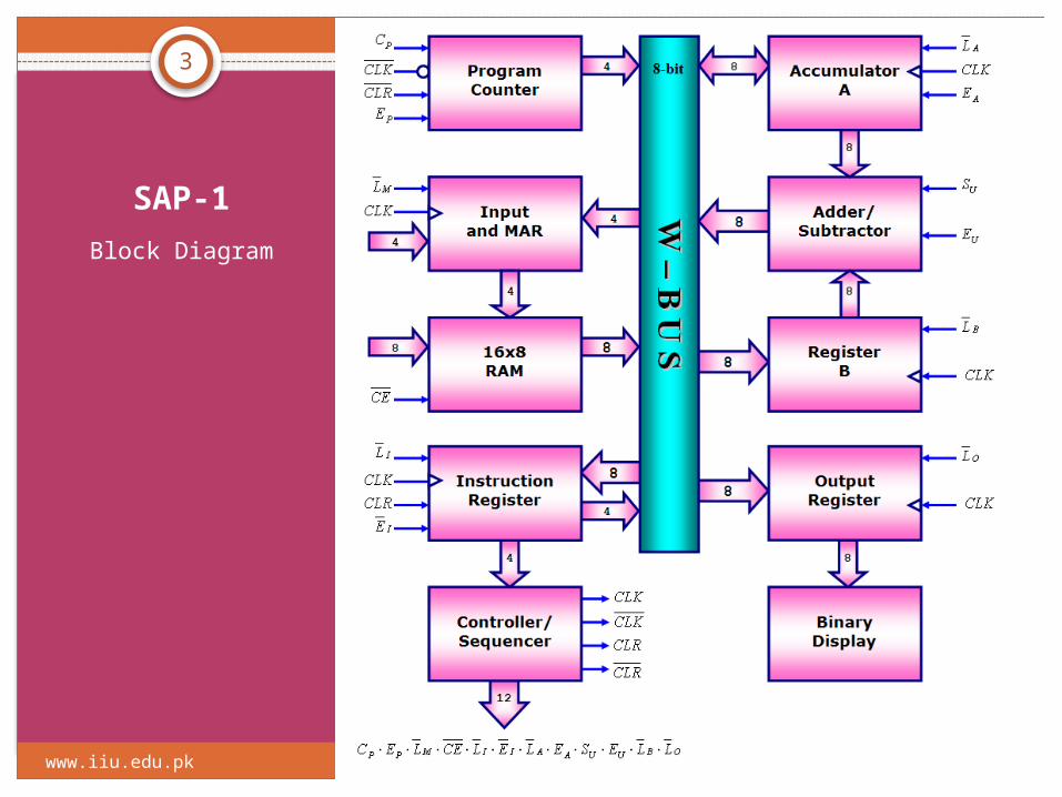
SAP-1 Introduction
SAP-1 is the first stage in the evolution towards modern computers.
The main purpose of SAP is to introduce all the crucial ideas behind computer operations.
Being a simple computer, SAP-1 also covers many advanced concepts.
SAP-1 is a bus organized computer. All registers are connected to the W bus with the help of tri-state buffers.
3
Saturday, April 15, 2023www.iiu.edu.pk
SAP-1Block Diagram
Saturday, April 15, 2023www.iiu.edu.pk
4
Main Features
Simple-As-Possible.One output device with 8 LEDs16 bytes of read only memory.5 instructions
3 with 1 operand, 2 with implicit operands.
Accumulator Architecture Accumulator, Out Register, B Register, Memory Address Register (MAR) Instruction Register (IR).
Saturday, April 15, 2023www.iiu.edu.pk
5
Architecture
8-bit "W" bus.4-bit program counter, only counts up, it starts counting
from 0 and counts up to 15.4-bit Memory Address Register (MAR).16 Byte Memory.8-bit (1 Byte) Instruction Register (IR).6-cycle controller with 12-bit microinstruction word.8-bit Accumulator.8-bit B Register.8-bit adder/subtractor.8-bit Output Register.

Saturday, April 15, 2023www.iiu.edu.pk
6
Saturday, April 15, 2023www.iiu.edu.pk
7
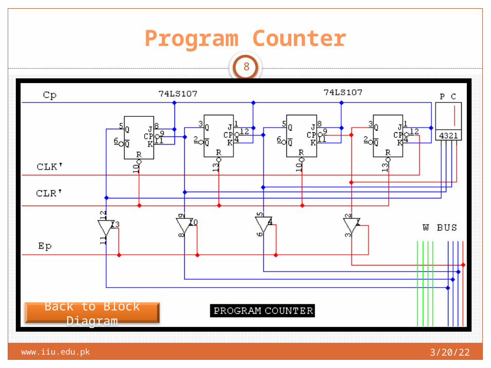
Program Counter
Instructions to be executed are placed at the starting addresses of memory, e.g. the first instruction of a program will be placed at binary address 0000. the second at address 0001.
Now to execute one instruction, first step is to generate the address at which this instruction is placed in memory.
So this address is generated by (4-bit) Program Counter, that counts from 0000 to 1111 (for total of 16 memory locations).
If the value of program counter is 0100, then the instruction at address at 4 will be executes next.
program counter is like a pointer register; it points to the address of next instruction to be executed.
Saturday, April 15, 2023www.iiu.edu.pk
8
Program Counter
Back to Block Diagram

Saturday, April 15, 2023www.iiu.edu.pk
9
Input and Memory Address Register (MAR)
The MAR stores the (4-bit) address of data and instruction which are placed in memory.
When SAP-1 is Running Mode, the (4-bit) address is generated by the Program Counter which is then stored into the MAR through W bus.
A bit later, the MAR applies this 4-bit address to the RAM, where Data or instruction is read from RAM.
In Simulation we are using first 16 locations (0 to 15) of a 32x8 PROM.

Saturday, April 15, 2023www.iiu.edu.pk
10
Back to Block Diagram
Saturday, April 15, 2023www.iiu.edu.pk
11
The RAM
In initial design, the RAM is a 16 x 8 static TTL RAM. It means there are 16 memory locations (from 0 to 15) and each location contains an 8-bit of data/instruction.
You can program the RAM by means of the switches to be used for address and data. This allows you to store a program and data in the memory before a computer run.
During a computer run, the RAM receives 4-bit addresses from the MAR and a read operation is performed,
in this way, the instruction or data stored in the RAM is placed on the W bus for use in some other part of the computer.

Saturday, April 15, 2023www.iiu.edu.pk
12
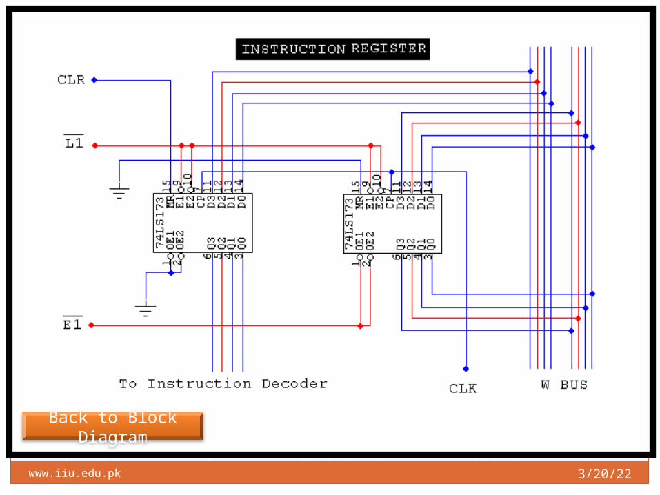
Intruction Register
When the instruction is placed at W-bus from memory, the Instruction Register stores this instruction on the next positive clock edge.
The contents of the instruction register are split into two nibbles. The upper nibble is a two-state output that goes directly to the
block labeled "Controller-sequencer“ The lower nibble is a three-state output that is read onto the W
bus when needed.
Saturday, April 15, 2023www.iiu.edu.pk
13
Back to Block Diagram
Saturday, April 15, 2023www.iiu.edu.pk
14
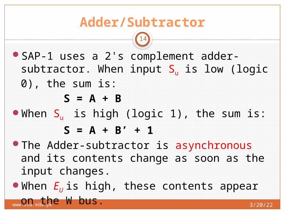
Adder/Subtractor
SAP-1 uses a 2's complement adder-subtractor. When input Su is low (logic 0), the sum is:
S = A + BWhen Su is high (logic 1), the sum is:
S = A + B’ + 1The Adder-subtractor is asynchronous and its contents
change as soon as the input changes.When EU is high, these contents appear on the W bus.

Saturday, April 15, 2023www.iiu.edu.pk
15
Back to Block Diagram
Saturday, April 15, 2023www.iiu.edu.pk
16
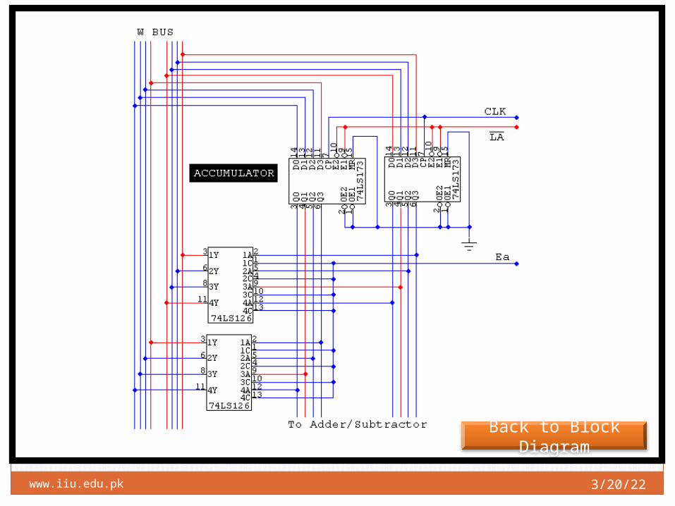
Accumulator
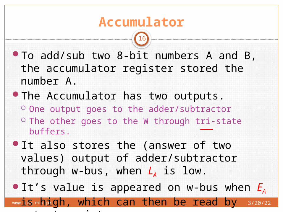
To add/sub two 8-bit numbers A and B, the accumulator register stored the number A.
The Accumulator has two outputs. One output goes to the adder/subtractor The other goes to the W through tri-state buffers.
It also stores the (answer of two values) output of adder/subtractor through w-bus, when LA is low.
It’s value is appeared on w-bus when EA is high, which can then be read by output register.
Saturday, April 15, 2023www.iiu.edu.pk
17
Back to Block Diagram

Saturday, April 15, 2023www.iiu.edu.pk
18
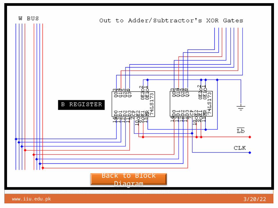
B Register
To add/sub two 8-bit numbers A and B, the B register stored the number B.
It supplies the number to be added or subtracted from the contents of accumulator to the adder/subtractor.
When data is available at W-bus and Lb goes low, at the positive clock edge, B register loads that data.
Saturday, April 15, 2023www.iiu.edu.pk
19
Back to Block Diagram
Saturday, April 15, 2023www.iiu.edu.pk
20
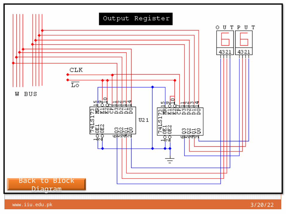
Output Register
At the end of an arithmetic operation the accumulator contains the word representing the answer,
Then answer stored in the accumulator register is then loaded into the output register through W-bus.
This is done in the next positive clock edge when EA is high and LO is low.
Now this value can be displayed to the outside world with the help of LEDs or 7 Segments.
Saturday, April 15, 2023www.iiu.edu.pk
21
Back to Block Diagram

Saturday, April 15, 2023www.iiu.edu.pk
22
Binary Display
The binary display is a row of eight light-emitting diodes (LEDs).
Because each LED connects to one flip-flop of the output port, the binary display shows us the contents of the output port.
Therefore, after we've transferred an answer from the accumulator to the output port, we can see the answer in binary form.
But we are using 7-segments in simulation.

Saturday, April 15, 2023www.iiu.edu.pk
23
Controller Sequencer
The 12 bits coming out of the Controller Sequencer form a word that controls the rest of the computer. Before each operation a Clear (CLR) signal resets the computer.
The 12 wires carrying the control word are called the Control Bus. The control word has the format:
This word determines how the registers will react to the next
positive clock (CLK) edge. For instance a high and a low means that the contents of Program Counter are latched into MAR on the next positive clock edge. As another example, a low and a low mean that the addressed RAM word will be transferred to the accumulator on the next positive clock edge.
CON CELEC MPP AA ELEL 11 OBUU LLES
Saturday, April 15, 2023www.iiu.edu.pk
24
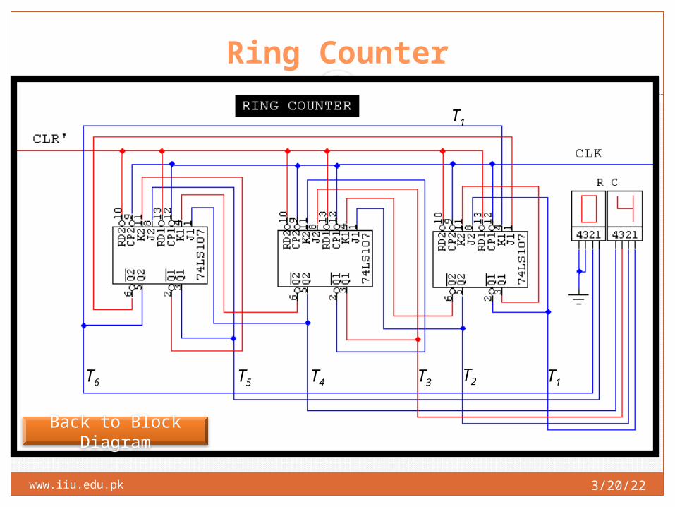
Ring Counter
Back to Block Diagram
T1
T6 T5 T4 T3 T2 T1
Saturday, April 15, 2023www.iiu.edu.pk
25
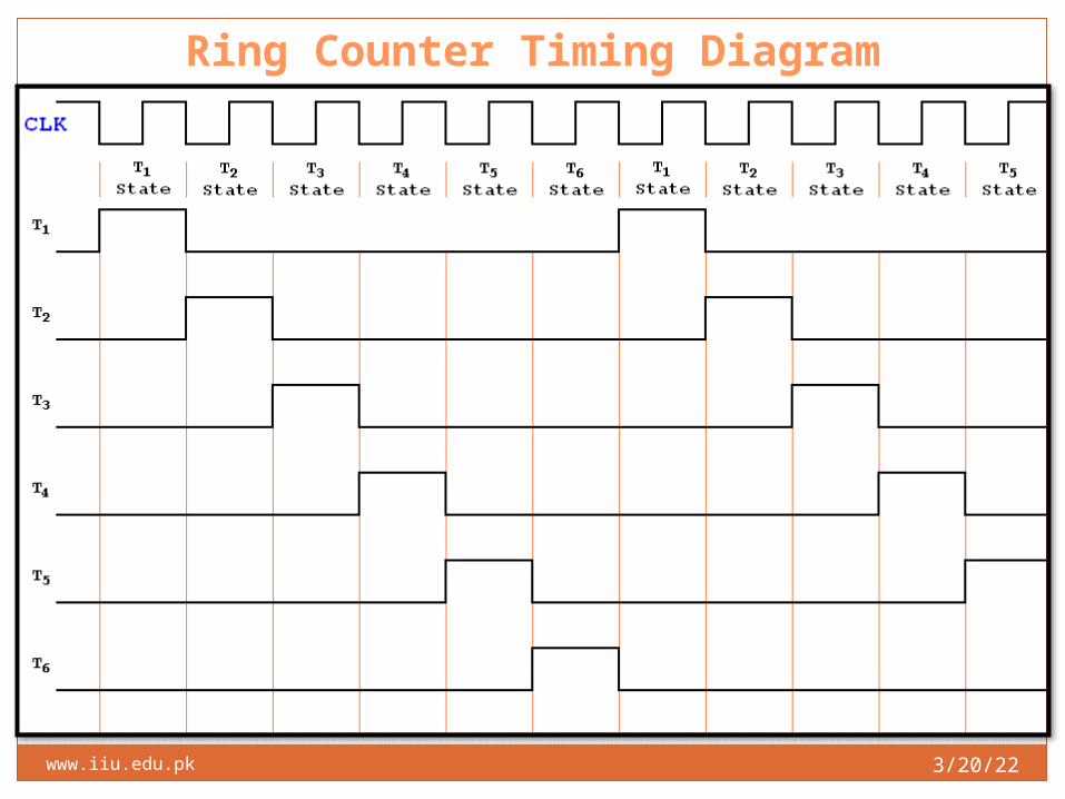
Ring Counter Timing Diagram

Saturday, April 15, 2023www.iiu.edu.pk
26
Back to Block Diagram

Saturday, April 15, 2023www.iiu.edu.pk
27
Control Matrix
Back to Block Diagram

Saturday, April 15, 2023www.iiu.edu.pk
28
Control Matrix
Back to Block Diagram
Saturday, April 15, 2023www.iiu.edu.pk
29
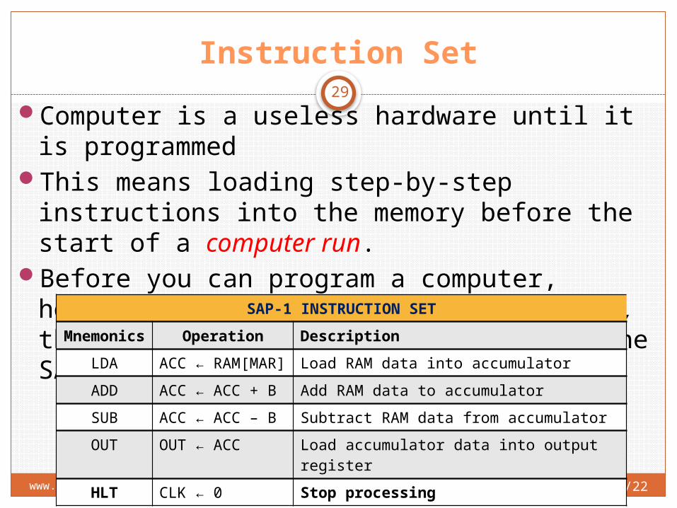
Instruction Set
Computer is a useless hardware until it is programmedThis means loading step-by-step instructions into the
memory before the start of a computer run.Before you can program a computer, however, you must
learn its instruction set, the basic operations it can perform. The SAP-1 instruction set follows.
SAP-1 INSTRUCTION SET
Mnemonics Operation Description
LDA ACC ← RAM[MAR] Load RAM data into accumulator
ADD ACC ← ACC + B Add RAM data to accumulator
SUB ACC ← ACC – B Subtract RAM data from accumulator
OUT OUT ← ACC Load accumulator data into output register
HLT CLK ← 0 Stop processing

Saturday, April 15, 2023www.iiu.edu.pk
30
LDA Instruction
LDA stands for "load the accumulator," A complete LDA instruction includes the hexadecimal address of the data to be loaded.
For example, LDA 8H means “load the accumulator with the contents of memory location 8H.”
Therefore, given RAM[8] = 1111 0000
The execution of LDA 8H results in ACC = 1111 0000Similarly. LDA FH means "load the accumulator with
the contents of memory location FH.

Saturday, April 15, 2023www.iiu.edu.pk
31
ADD Instruction
ADD 9H means “add the data of memory location 9H with data of accumulator and save the result in accumulator.
Suppose No. 2 is in the accumulator and No.3 is in memory location 9H. Then ACC =0000 0010, RAM[9] = 0000 0011
During the execution of ADD 9H, First data at RAM address 9 is loaded into the B register to get B = 0000
0011 and instantly the adder/subtracter forms the sum of A and B SUM = 0000 0101
Second, this sum is loaded into the accumulator to get ACC = 0000 0101
Similarly, the execution of ADD FH adds data at RAM address 15 to the accumulator and save the answer back in accumulator overwriting the previous value.
The negative numbers are stored in 2’s complement form.
Saturday, April 15, 2023www.iiu.edu.pk
32
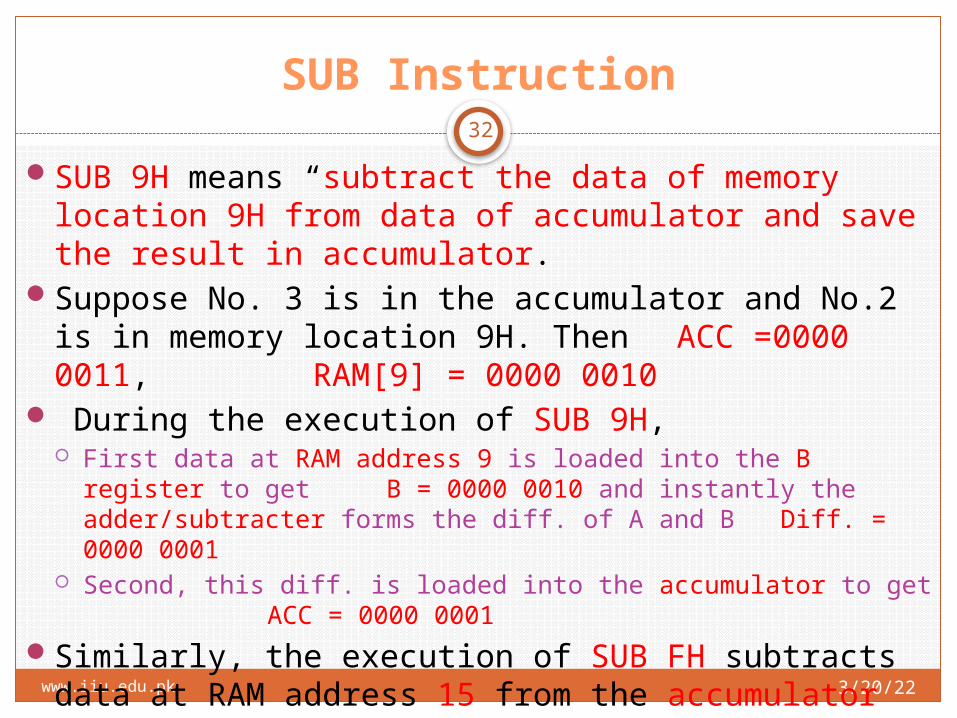
SUB Instruction
SUB 9H means “subtract the data of memory location 9H from data of accumulator and save the result in accumulator.
Suppose No. 3 is in the accumulator and No.2 is in memory location 9H. Then ACC =0000 0011, RAM[9] = 0000 0010
During the execution of SUB 9H, First data at RAM address 9 is loaded into the B register to get B = 0000
0010 and instantly the adder/subtracter forms the diff. of A and B Diff. = 0000 0001
Second, this diff. is loaded into the accumulator to get ACC = 0000 0001
Similarly, the execution of SUB FH subtracts data at RAM address 15 from the accumulator and save the answer back in accumulator overwriting the previous value.
Saturday, April 15, 2023www.iiu.edu.pk
33
OUT Instruction
The instruction OUT tells the SAP-1 computer to transfer the accumulator contents to the output port.
After OUT has been executed, you can see the answer to the problem being solved on LEDs display.
OUT is complete by itself; that is, you do not have to include an address when using OUT because the instruction does not involve data in the memory.

Saturday, April 15, 2023www.iiu.edu.pk
34
HLT Instruction
HLT stands for halt. This instruction tells the computer to stop processing data so it stops the clock.
HLT marks the end of a program, similar to the way a period marks the end of a sentence.
You must use a HLT instruction at the end of every SAP-1 program; otherwise, you get computer trash (meaningless answers caused by runaway processing).
HLT is complete by itself; you do not have to include a RAM word when using HLT because this instruction does not involve the memory.

Saturday, April 15, 2023www.iiu.edu.pk
35
Memory Reference Instructions
LDA, ADD, and SUB are called memory-reference instructions because they use data stored in the memory.
OUT and HLT, on the other hand, are not memory reference instructions because they do not involve the data stored in the memory.
Mnemonics LDA, ADD, SUB, OUT, and HLT are the instruction set for
SAP-1. Abbreviated instructions like these are called mnemonics (memory aids). Mnemonics are popular in computer work because they remind you of the operation that will take place when the instruction is executed.
Saturday, April 15, 2023www.iiu.edu.pk
36
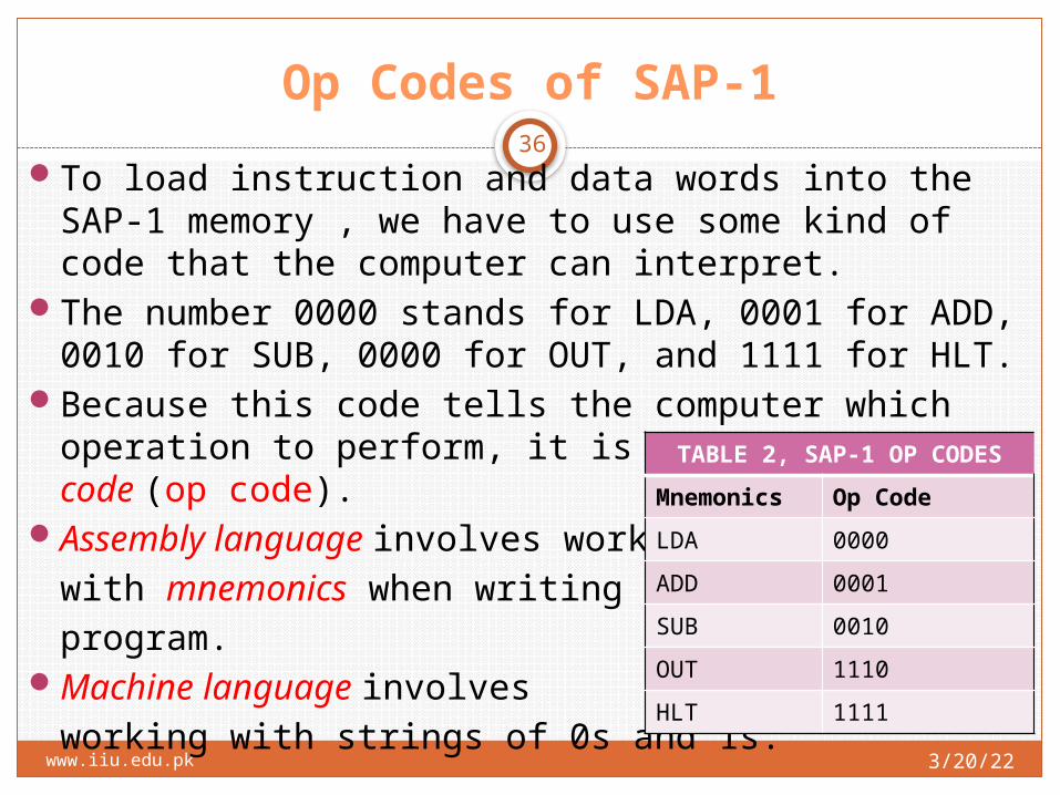
Op Codes of SAP-1
To load instruction and data words into the SAP-1 memory , we have to use some kind of code that the computer can interpret.
The number 0000 stands for LDA, 0001 for ADD, 0010 for SUB, 0000 for OUT, and 1111 for HLT.
Because this code tells the computer which operation to perform, it is called an operation code (op code).
Assembly language involves workingwith mnemonics when writing a program.
Machine language involvesworking with strings of 0s and 1s.
TABLE 2, SAP-1 OP CODES
Mnemonics Op Code
LDA 0000
ADD 0001
SUB 0010
OUT 1110
HLT 1111

Saturday, April 15, 2023www.iiu.edu.pk
37
Program in Assembly
Address Contents
0H LDA 9H
1H ADD AH
2H ADD CH
3H SUB BH
4H OUT
5H HLT
6H FFH
7H FFH
8H FFH
9H 10H
AH 18H
BH 14H
CH 20H
DH FFH
EH FFH
FH FFH
Program in Machine Language
Address Contents in Binary Contents in Hexadecimal
0000 0000 1001 09H
0001 0001 1010 1AH
0010 0001 1100 1CH
0011 0010 1011 2BH
0100 1110 1111 EFH
0101 1111 1111 FFH
0110 1111 1111 FFH
0111 1111 1111 FFH
1000 1111 1111 FFH
1001 0001 0000 10H
1010 0001 1000 18H
1011 0001 0100 14H
1100 0010 0000 20H
1101 1111 1111 FFH
1110 1111 1111 FFH
1111 1111 1111 FFH
Saturday, April 15, 2023www.iiu.edu.pk
38
The 8080 and 8085 Microprocessors
The 8080 was the first widely used microprocessor.It has 72 instructions. The 8085 is an enhanced
version of the 8080 with essentially the same instruction set (both are designed by Intel Corp.).
The SAP-1 instructions are upward compatible with the 8080/8085 instruction set.
In other words, the SAP-1 instructions LDA, ADD, SUB, OUT, and HLT are 8080/8085 instructions.
Learning SAP instructions is getting you ready for the 8080 and 8085, two widely used microprocessors.
Saturday, April 15, 2023www.iiu.edu.pk
39
Fetch Cycle
The control unit is the key to a computer's automatic operation. The control unit generates the control words that fetch and execute each instruction.
While each instruction is fetched and executed, the computer passes through different timing states (T states), time intervals during which register contents change.
Ring Counter has an output of T = T6T5T4T3T2T1
At the beginning of a computer run, the ring word isT = 00 0001 = T1
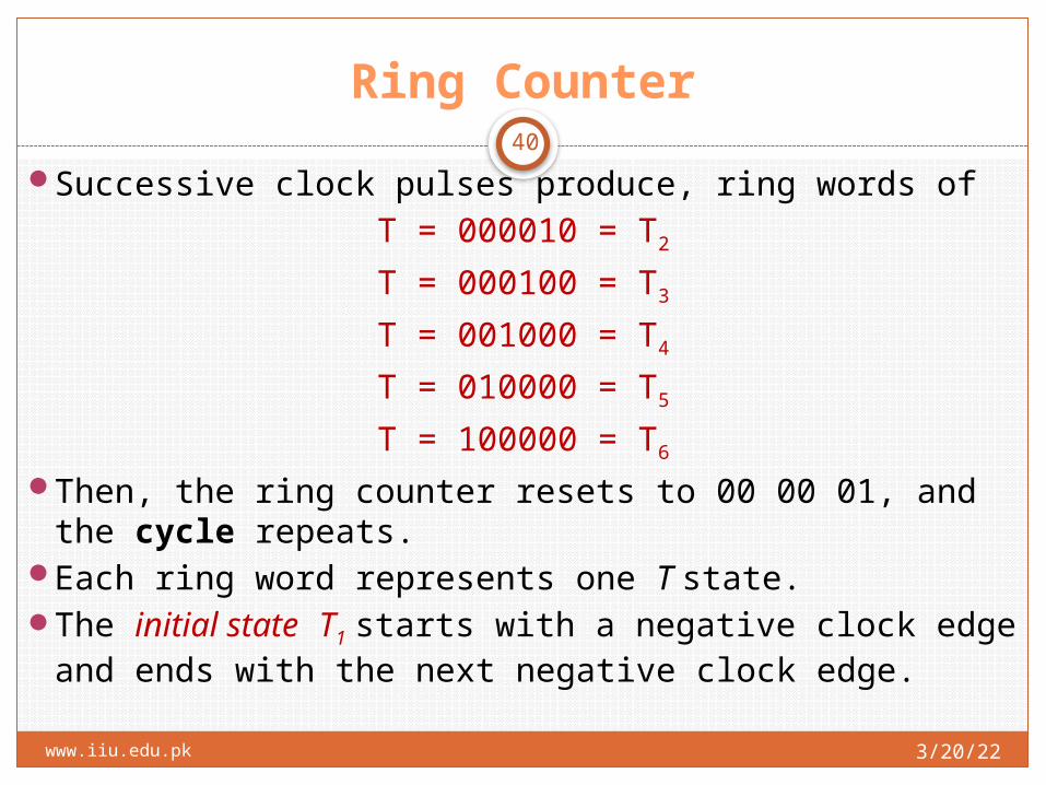
Successive clock pulses produce, ring words of
Saturday, April 15, 2023www.iiu.edu.pk
40
Ring Counter
Successive clock pulses produce, ring words ofT = 000010 = T2
T = 000100 = T3
T = 001000 = T4
T = 010000 = T5
T = 100000 = T6
Then, the ring counter resets to 00 00 01, and the cycle repeats.
Each ring word represents one T state.The initial state T1 starts with a negative clock edge and ends
with the next negative clock edge.
Saturday, April 15, 2023www.iiu.edu.pk
41
Ring Counter
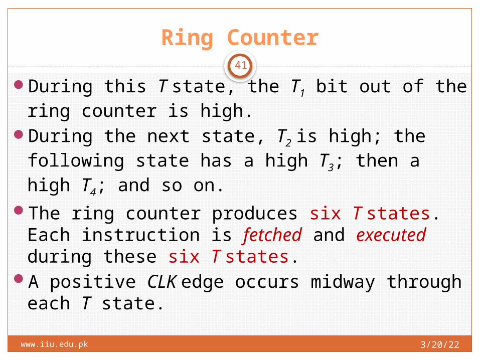
During this T state, the T1 bit out of the ring counter is high.
During the next state, T2 is high; the following state has a high T3; then a high T4; and so on.
The ring counter produces six T states. Each instruction is fetched and executed during these six T states.
A positive CLK edge occurs midway through each T state.
Saturday, April 15, 2023www.iiu.edu.pk
42
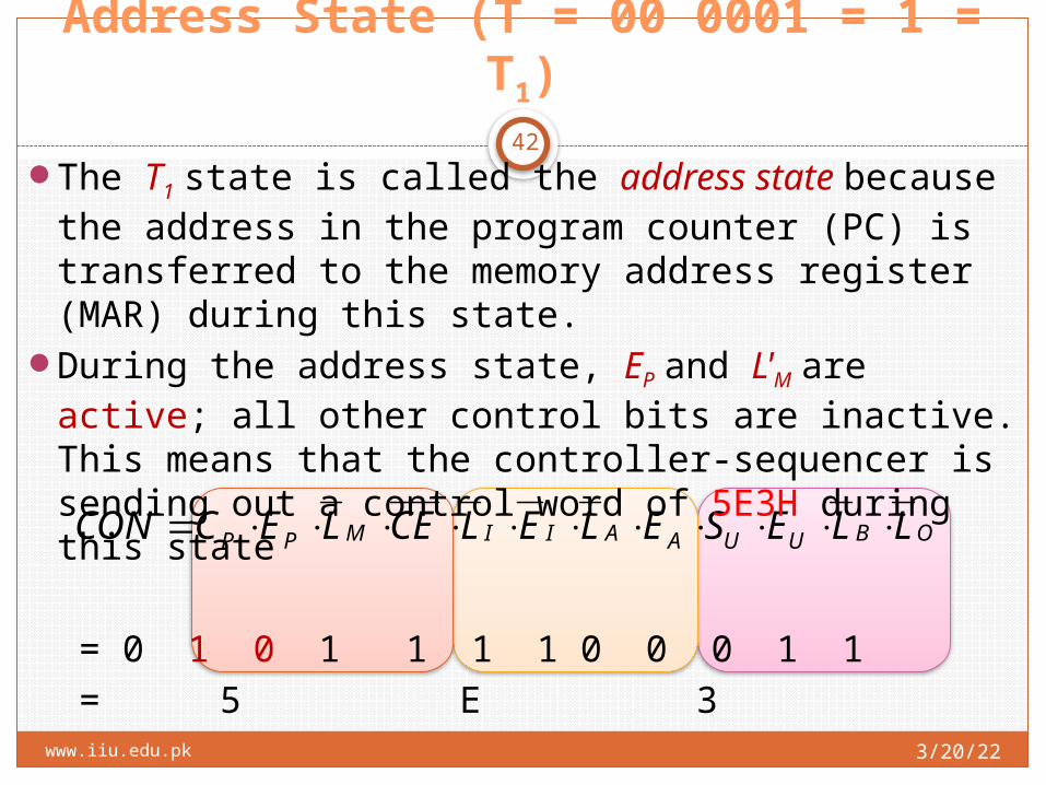
Address State (T = 00 0001 = 1 = T1)
OBUUAAIIMPP LLESELELCELECCON
The T1 state is called the address state because the address in the program counter (PC) is transferred to the memory address register (MAR) during this state.
During the address state, EP and L'M are active; all other control bits are inactive. This means that the controller-sequencer is sending out a control word of 5E3H during this state
= 0 1 0 1 1 1 1 0 0 0 1
1 = 5 E 3

Saturday, April 15, 2023www.iiu.edu.pk
43
Increment State (T = 00 0010 = 2 = T2)
OBUUAAIIMPP LLESELELCELECCON
The T1 state is called the increment state because the program counter is incremented.
During the increment state, the controller-sequencer is producing a control word of BE3H
Only the CP bit is active in this state.
= 1 0 1 1 1 1 1 0 0 0 1 1
= B E 3
Saturday, April 15, 2023www.iiu.edu.pk
44
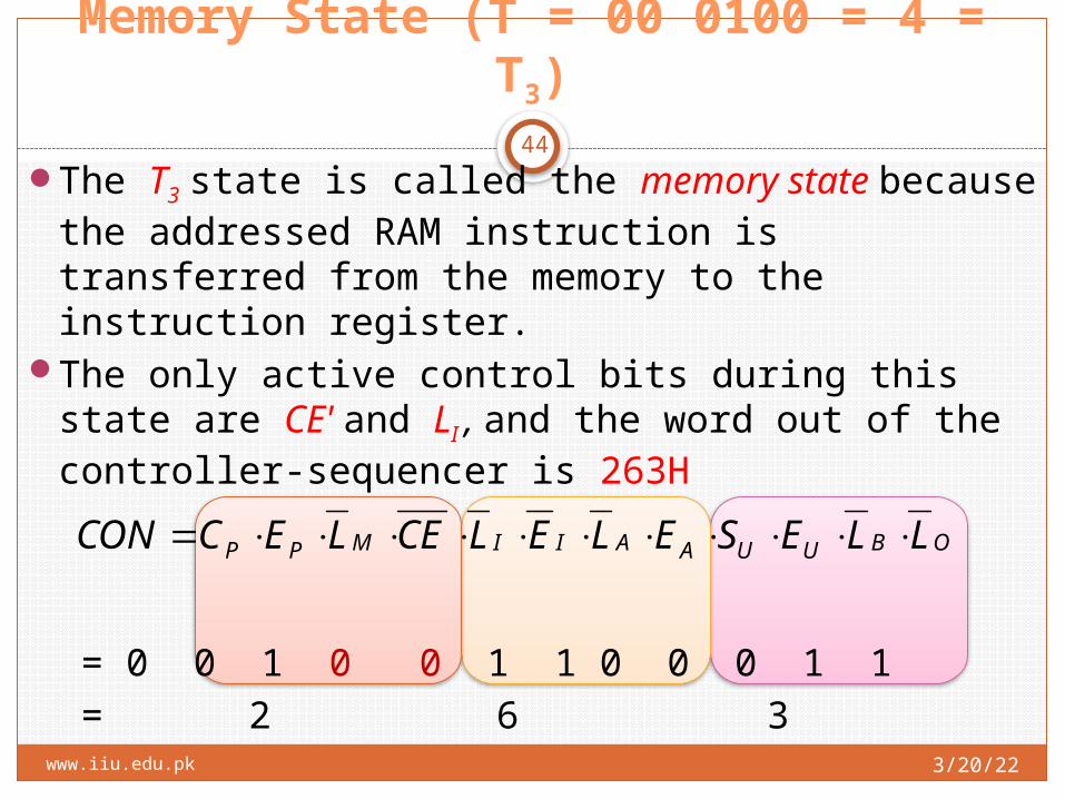
Memory State (T = 00 0100 = 4 = T3)
OBUUAAIIMPP LLESELELCELECCON
The T3 state is called the memory state because the addressed RAM instruction is transferred from the memory to the instruction register.
The only active control bits during this state are CE' and LI , and the word out of the controller-sequencer is 263H
= 0 0 1 0 0 1 1 0 0 0 1 1
= 2 6 3
Saturday, April 15, 2023www.iiu.edu.pk
45
Fetch Cycle
The address, increment, and memory states are called the fetch cycle of SAP-l.
During the address state, EP and LM arc active; this means that the program counter sets up the MAR via the W bus.
A positive clock edge occurs midway through the address state; this loads the MAR with the contents of the PC.
During the increment state, CP is the only active control bit.This sets up the program counter to count positive clock edges.
Halfway through the increment state, a positive clock edge hits the program counter and advances the count by 1.
During the memory state, CE' and L'I are active. The addressed RAM
word sets up the instruction register via the W bus. Midway through the memory state, a positive clock edge loads the instruction register with the addressed RAM word.

Saturday, April 15, 2023www.iiu.edu.pk
46
Execution Cycle
The next three states (T4, T5, and T6) are the execution cycle of SAP-1.
The register transfers during the execution cycle depend on the particular instruction being executed.
For instance. LDA 9H requires different register transfers than ADD BH.
What follows are the control routines for different SAP-1 instructions.

Saturday, April 15, 2023www.iiu.edu.pk
47
Micro Instructions
The controller-sequencer sends out control words, on during each T state or clock cycle.
These words are like directions telling the rest of the computer what to do.
Because it produces a small step in the data processing, each control word is called a micro-instruction.

Saturday, April 15, 2023www.iiu.edu.pk
48
Macro Instructions
The instructions we have been programming with (LDA, ADD, SUB, . . .) are sometimes called macro-instructions to distinguish them from micro-instructions.
Each SAP-1 macroinstruction is made up of three microinstructions. For example, the LDA macroinstruction consists of the three microinstructions shown in the next Table.
This table shows the SAP-1 macro-instruction and the micro-instructions needed to carry it out.

Saturday, April 15, 2023www.iiu.edu.pk
49
Fetch and Execute Cycle of SAP-1
Macro Inst. T State Micro Operation Active CON
All Instructions
T1 MAR ← PC L'M, EP 5E3H
T2 PC← PC+1 CP BE3H
T3 IR ← RAM[MAR] CE', L‘I 263H
LDA T4 MAR ← IR(3…0) L'M, E‘I 1A3H
T5 ACC ← RAM[MAR] CE', L'A 2C3H
T6 None None 3E3H
ADD T4 MAR ← IR(3…0) L'M, E‘I 1A3H
T5 B ← RAM[MAR] CE', L'B 2E1H
T6 ACC ← ACC+B L'A, EU 3C7H
SUB T4 MAR ← IR(3…0) L'M, E‘I 1A3H
T5 B ← RAM[MAR] CE', L'B 2E1H
T6 ACC ← ACC – B L'A, SU, EU 3CFH
OUT T4 OUT ← ACC EA, L'O 3F2H
T5 None None 3E3H
T6 None None 3E3H
HLT T3 None HLT ' 263H

50
Saturday, April 15, 2023www.iiu.edu.pk
SAP-1
Simulation of Program
LDA 9H
ADD AH
OUT
HLT
00000001
0000 1001
0000
1001
0000 01010001 1010
0010
0001
1010
0000 0011
0000 1000
0011
1110 1111
1110
0000 1000
08
0100
1111 1111
1111
T1T2T3T4T5T6T1T2T3T4T5T6T1T2T3T4T5T6T1T2T3Computer
Halted

Saturday, April 15, 2023www.iiu.edu.pk 51
That’s all
Related Documents