SAMSUNG FOUNDRY Strong 14nm FinFET Logic Process and Design Infrastructure for Advanced Mobile SOC Applications Samsung Foundry’s advanced 14-nanometer (nm) FinFET process technology offers a robust design infrastructure to drive future mobile application markets. As mobile applications continue to demand a more PC-like user experience, Samsung’s FinFET process technology enables system-on-chip (SOC) designers to reap all of the advantages for the latest energy-efficient processors: die-size reductions, faster frequencies, and lower power consumption. FIG. 1 Samsung 14nm FinFET process technology addresses the power reduction breakthrough that is needed to meet mobile power requirements. POWER 100% POWER GAP 200% POWER BUDGET POWER CONSUMPTION

Welcome message from author
This document is posted to help you gain knowledge. Please leave a comment to let me know what you think about it! Share it to your friends and learn new things together.
Transcript

SamSung Foundry
Strong 14nm FinFET Logic Process and Design Infrastructure for Advanced Mobile SOC Applications
Samsung Foundry’s advanced 14-nanometer (nm) FinFET process technology offers a robust design infrastructure to drive future mobile
application markets. As mobile applications continue to demand a more PC-like user experience, Samsung’s FinFET process technology
enables system-on-chip (SOC) designers to reap all of the advantages for the latest energy-efficient processors: die-size reductions, faster
frequencies, and lower power consumption.
FIg. 1 Samsung 14nm FinFET process technology addresses the power reduction breakthrough that is needed to meet mobile power requirements.
Po
WE
r
100%
PoWEr gaP
200%
PoWEr BudgET
PoWEr ConSumPTIon
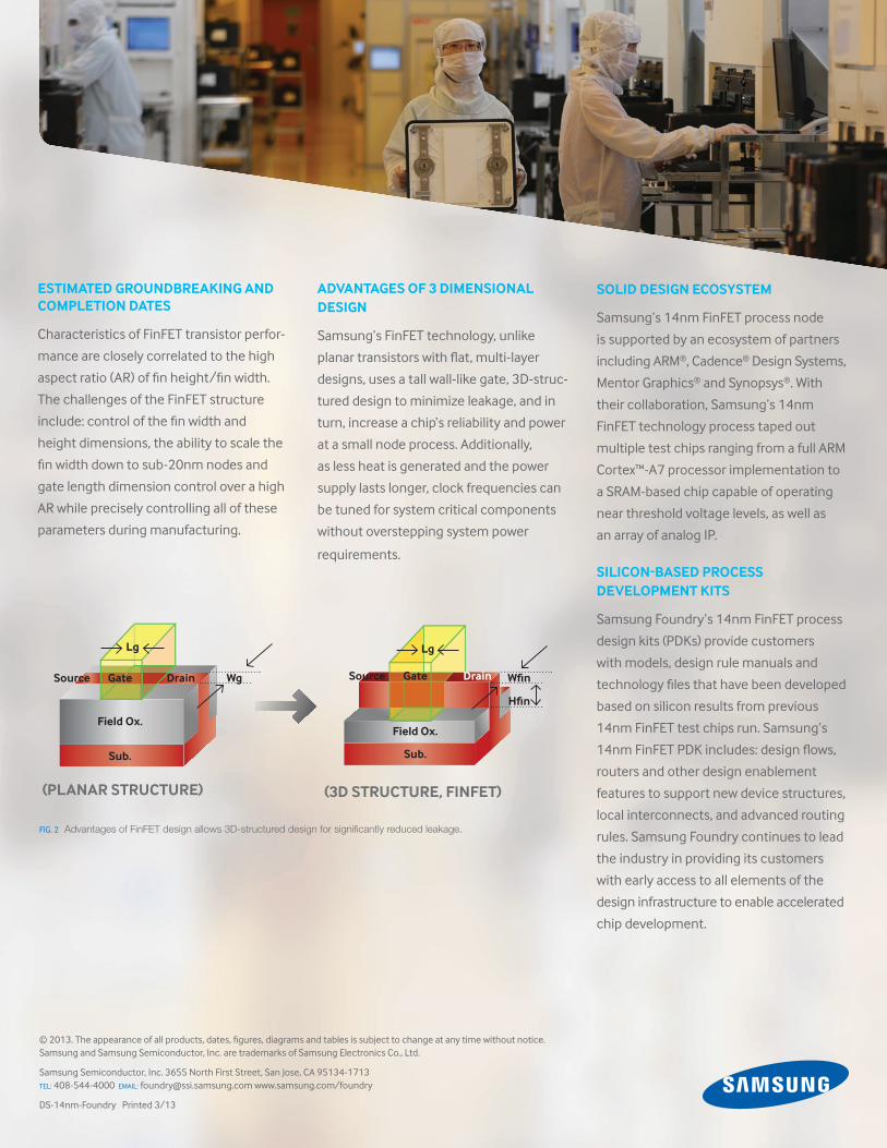
FIg. 2 Advantages of FinFET design allows 3D-structured design for significantly reduced leakage.
(3d STruCTurE, FInFET)
Lg
Source gate
Field ox.
Sub.
Wfin
Hfin
Drain
(PLanar STruCTurE)
Lg
Source gate
Field ox.
Sub.
Drain Wg
ESTImaTEd groundBrEakIng and ComPLETIon daTES
Characteristics of FinFET transistor perfor-
mance are closely correlated to the high
aspect ratio (AR) of fin height/fin width.
The challenges of the FinFET structure
include: control of the fin width and
height dimensions, the ability to scale the
fin width down to sub-20nm nodes and
gate length dimension control over a high
AR while precisely controlling all of these
parameters during manufacturing.
advanTagES oF 3 dImEnSIonaL dESIgn
Samsung’s FinFET technology, unlike
planar transistors with flat, multi-layer
designs, uses a tall wall-like gate, 3D-struc-
tured design to minimize leakage, and in
turn, increase a chip’s reliability and power
at a small node process. Additionally,
as less heat is generated and the power
supply lasts longer, clock frequencies can
be tuned for system critical components
without overstepping system power
requirements.
SoLId dESIgn ECoSySTEm
Samsung’s 14nm FinFET process node
is supported by an ecosystem of partners
including ARM®, Cadence® Design Systems,
Mentor graphics® and Synopsys®. With
their collaboration, Samsung’s 14nm
FinFET technology process taped out
multiple test chips ranging from a full ARM
Cortex™-A7 processor implementation to
a SRAM-based chip capable of operating
near threshold voltage levels, as well as
an array of analog IP.
SILICon-BaSEd ProCESS dEvELoPmEnT kITS
Samsung Foundry’s 14nm FinFET process
design kits (PDKs) provide customers
with models, design rule manuals and
technology files that have been developed
based on silicon results from previous
14nm FinFET test chips run. Samsung’s
14nm FinFET PDK includes: design flows,
routers and other design enablement
features to support new device structures,
local interconnects, and advanced routing
rules. Samsung Foundry continues to lead
the industry in providing its customers
with early access to all elements of the
design infrastructure to enable accelerated
chip development.
© 2013. The appearance of all products, dates, figures, diagrams and tables is subject to change at any time without notice. Samsung and Samsung Semiconductor, Inc. are trademarks of Samsung Electronics Co., Ltd.
Samsung Semiconductor, Inc. 3655 North First Street, San Jose, CA 95134-1713 TEL: 408-544-4000 EMAIL: [email protected] www.samsung.com/foundry
DS-14nm-Foundry Printed 3/13
Related Documents