Safe Start-up Procedures of Isolated Bi-directional DC-DC Converter Franc Mihalič and Alenka Hren University of Maribor, Faculty of Electrical Engineering and Computer Science Smetanova 17, 2000 Maribor, Slovenia, e-mail: [email protected], alenka.hren @uni-mb.si Abstract — This paper presents a safe start-up procedures of an isolated bi-directional DC-DC converter in buck and boost modes. This converter has been developed as a part of multifunctional up to 4 kW power supply system that uses a high voltage (450 V) DC-link. The isolated bi-directional DC-DC converter can charge 28 V batteries and supply auxiliary low voltage DC loads. Additionally, the isolated bi- directional converter can also draw power from the batteries or from truck’s engine driven alternator to keep maintain the high voltage DC-link. Modulation strategies, start-up procedures and control of this converter have been validated by using the Matlab SymPowerSystems Toolboxes and finally, they have been also experimentally verified. Keywords — Switched mode power supply, Converter circuit, Pulse Width Modulation (PWM), Safety I. INTRODUCTION Isolated bi-directional DC-DC converters are commonly used in electronic equipment such as Uninterruptible Power Supplies (UPS), electric vehicles and as front-end converters for distributed power system applications, among others [1]. In all applications the key features are the safety of the system operation and operation at the highest possible efficiency [2], [3]. A block diagram of the isolated bi-directional DC-DC converter based on full-bridge topologies is shown in Fig. 1. Isolated bi-directional DC-DC converter is the combined configuration of battery charging circuit and DC-DC converter circuit. It allows power flow in both directions, i.e. towards the battery and from the battery Fig. 1. Block diagram of the bi-directional DC-DC converter. and has a wide range of applications from uninterrupted power supplies, battery charging and discharging systems, aerospace applications to auxiliary power supplies for hybrid electrical vehicles. Specially, low-loss, constant- frequency, zero-voltage-switching (ZVS) modulation strategy for bi-directional, cascaded, buck-boost DC-DC converters with high power density are used in hybrid electrical vehicles (HEVs) or fuel cell vehicles (FCVs) [4]. Possible implementation of bi-directional converters are with: half bridge topology where PWM pulses are generated by application of artificial neural network controller (ANN) [5], full bridge topology using resonant [6], soft switching and hard switching [7] has been reported in literature. Each implementation has its advantages and disadvantages as are higher component ratings, increased circuit complexity, loss of switching signals at light load for soft switch circuit etc. In this paper, the full bridge topologies bi-directional DC-DC converter (shown in Fig. 2) using hard switch PWM with emphasis on the safe start-up procedures in boost- and buck mode operation will be discussed. Fig. 2. Isolated bi-directional DC-DC converter for buck- and boost-mode of operation. 14th International Power Electronics and Motion Control Conference, EPE-PEMC 2010 978-1-4244-7855-2/10/$26.00 ©2010 IEEE T2-167

Welcome message from author
This document is posted to help you gain knowledge. Please leave a comment to let me know what you think about it! Share it to your friends and learn new things together.
Transcript
Safe Start-up Procedures of Isolated Bi-directional DC-DC Converter
Franc Mihalič and Alenka Hren University of Maribor, Faculty of Electrical Engineering and Computer Science
Smetanova 17, 2000 Maribor, Slovenia, e-mail: [email protected], alenka.hren @uni-mb.si
Abstract — This paper presents a safe start-up procedures of an isolated bi-directional DC-DC converter in buck and boost modes. This converter has been developed as a part of multifunctional up to 4 kW power supply system that uses a high voltage (450 V) DC-link. The isolated bi-directional DC-DC converter can charge 28 V batteries and supply auxiliary low voltage DC loads. Additionally, the isolated bi-directional converter can also draw power from the batteries or from truck’s engine driven alternator to keep maintain the high voltage DC-link. Modulation strategies, start-up procedures and control of this converter have been validated by using the Matlab SymPowerSystems Toolboxes and finally, they have been also experimentally verified.
Keywords — Switched mode power supply, Converter circuit, Pulse Width Modulation (PWM), Safety
I. INTRODUCTION Isolated bi-directional DC-DC converters are
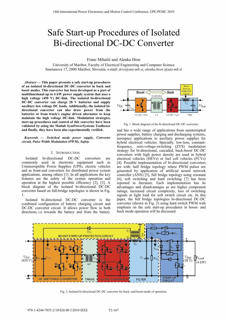
commonly used in electronic equipment such as Uninterruptible Power Supplies (UPS), electric vehicles and as front-end converters for distributed power system applications, among others [1]. In all applications the key features are the safety of the system operation and operation at the highest possible efficiency [2], [3]. A block diagram of the isolated bi-directional DC-DC converter based on full-bridge topologies is shown in Fig. 1.
Isolated bi-directional DC-DC converter is the combined configuration of battery charging circuit and DC-DC converter circuit. It allows power flow in both directions, i.e. towards the battery and from the battery
Fig. 1. Block diagram of the bi-directional DC-DC converter.
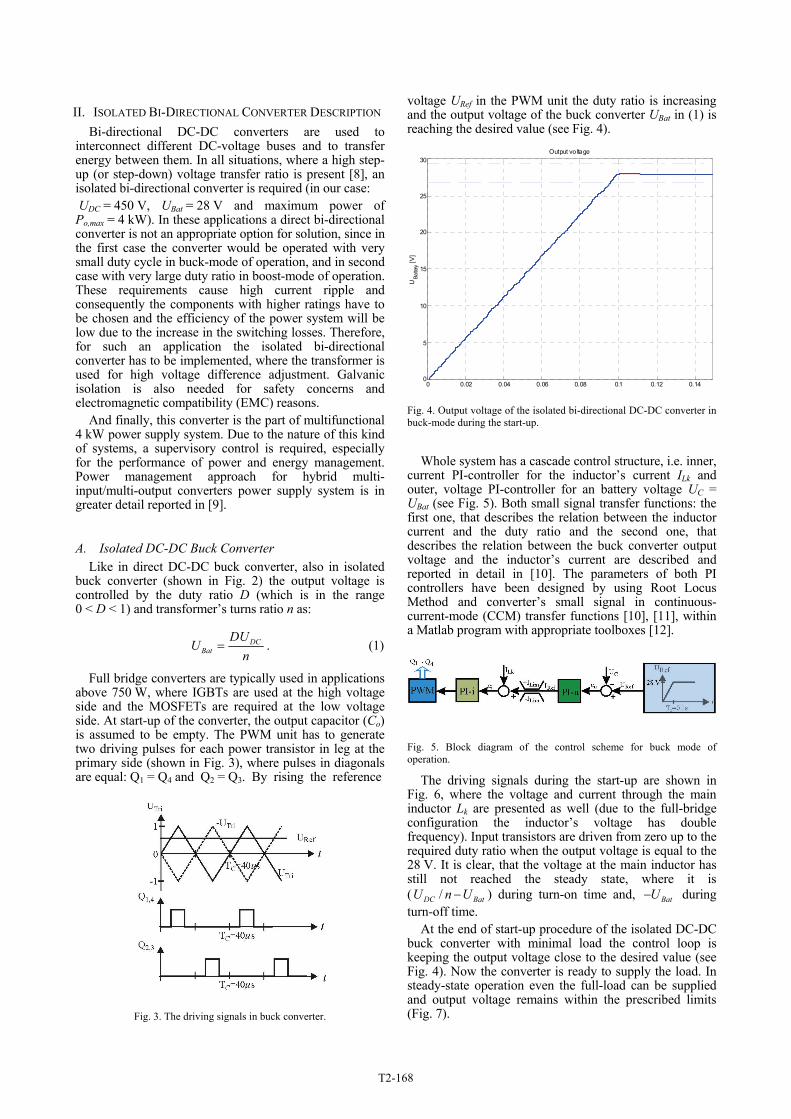
and has a wide range of applications from uninterrupted power supplies, battery charging and discharging systems, aerospace applications to auxiliary power supplies for hybrid electrical vehicles. Specially, low-loss, constant-frequency, zero-voltage-switching (ZVS) modulation strategy for bi-directional, cascaded, buck-boost DC-DC converters with high power density are used in hybrid electrical vehicles (HEVs) or fuel cell vehicles (FCVs) [4]. Possible implementation of bi-directional converters are with: half bridge topology where PWM pulses are generated by application of artificial neural network controller (ANN) [5], full bridge topology using resonant [6], soft switching and hard switching [7] has been reported in literature. Each implementation has its advantages and disadvantages as are higher component ratings, increased circuit complexity, loss of switching signals at light load for soft switch circuit etc. In this paper, the full bridge topologies bi-directional DC-DC converter (shown in Fig. 2) using hard switch PWM with emphasis on the safe start-up procedures in boost- and buck mode operation will be discussed.
Fig. 2. Isolated bi-directional DC-DC converter for buck- and boost-mode of operation.
14th International Power Electronics and Motion Control Conference, EPE-PEMC 2010
978-1-4244-7855-2/10/$26.00 ©2010 IEEE T2-167
II. ISOLATED BI-DIRECTIONAL CONVERTER DESCRIPTION Bi-directional DC-DC converters are used to
interconnect different DC-voltage buses and to transfer energy between them. In all situations, where a high step-up (or step-down) voltage transfer ratio is present [8], an isolated bi-directional converter is required (in our case: UDC = 450 V, UBat = 28 V and maximum power of Po,max = 4 kW). In these applications a direct bi-directional converter is not an appropriate option for solution, since in the first case the converter would be operated with very small duty cycle in buck-mode of operation, and in second case with very large duty ratio in boost-mode of operation. These requirements cause high current ripple and consequently the components with higher ratings have to be chosen and the efficiency of the power system will be low due to the increase in the switching losses. Therefore, for such an application the isolated bi-directional converter has to be implemented, where the transformer is used for high voltage difference adjustment. Galvanic isolation is also needed for safety concerns and electromagnetic compatibility (EMC) reasons.
And finally, this converter is the part of multifunctional 4 kW power supply system. Due to the nature of this kind of systems, a supervisory control is required, especially for the performance of power and energy management. Power management approach for hybrid multi-input/multi-output converters power supply system is in greater detail reported in [9].
A. Isolated DC-DC Buck Converter Like in direct DC-DC buck converter, also in isolated
buck converter (shown in Fig. 2) the output voltage is controlled by the duty ratio D (which is in the range 0 < D < 1) and transformer’s turns ratio n as:
DCBat
DUU
n= . (1)
Full bridge converters are typically used in applications above 750 W, where IGBTs are used at the high voltage side and the MOSFETs are required at the low voltage side. At start-up of the converter, the output capacitor (Co) is assumed to be empty. The PWM unit has to generate two driving pulses for each power transistor in leg at the primary side (shown in Fig. 3), where pulses in diagonals are equal: Q1 = Q4 and Q2 = Q3. By rising the reference
Fig. 3. The driving signals in buck converter.
voltage URef in the PWM unit the duty ratio is increasing and the output voltage of the buck converter UBat in (1) is reaching the desired value (see Fig. 4).
0 0.02 0.04 0.06 0.08 0.1 0.12 0.140
5
10
15
20
25
30
UBa
ttery [
V]
Output vo ltage
Fig. 4. Output voltage of the isolated bi-directional DC-DC converter in buck-mode during the start-up.
Whole system has a cascade control structure, i.e. inner,
current PI-controller for the inductor’s current ILk and outer, voltage PI-controller for an battery voltage UC = UBat (see Fig. 5). Both small signal transfer functions: the first one, that describes the relation between the inductor current and the duty ratio and the second one, that describes the relation between the buck converter output voltage and the inductor’s current are described and reported in detail in [10]. The parameters of both PI controllers have been designed by using Root Locus Method and converter’s small signal in continuous-current-mode (CCM) transfer functions [10], [11], within a Matlab program with appropriate toolboxes [12].
Fig. 5. Block diagram of the control scheme for buck mode of operation.
The driving signals during the start-up are shown in Fig. 6, where the voltage and current through the main inductor Lk are presented as well (due to the full-bridge configuration the inductor’s voltage has double frequency). Input transistors are driven from zero up to the required duty ratio when the output voltage is equal to the 28 V. It is clear, that the voltage at the main inductor has still not reached the steady state, where it is ( /DCU n UBat− ) during turn-on time and, BatU− during turn-off time.
At the end of start-up procedure of the isolated DC-DC buck converter with minimal load the control loop is keeping the output voltage close to the desired value (see Fig. 4). Now the converter is ready to supply the load. In steady-state operation even the full-load can be supplied and output voltage remains within the prescribed limits (Fig. 7).
T2-168
0.075 0.075 0.075 0.0751 0.0751 0.0751 0.0751 0.0751 0.0752 0.0752 0.07520
0.5
1
PW
MQ
1,2
Driving Signals
0.075 0.075 0.075 0.0751 0.0751 0.0751 0.0751 0.0751 0.0752 0.0752 0.0752
-20
0
20
ULk
[V]
Inductor´s voltage
0.075 0.075 0.075 0.0751 0.0751 0.0751 0.0751 0.0751 0.0752 0.0752 0.07520
5
10
15
20
I Lk [A
]
Inductor´s current
Fig. 6. Start-up of the isolated bi-directional DC-DC converter in buck-mode: driving signals for one transistor leg (top), inductor's voltage (middle) and inductor's current (bottom).
0.1 0.15 0.2 0.25 0.3 0.35 0.4 0.45 0.5 0.550
10
20
30
UBa
ttery
[V]
Steady state + full load ± 50%
0.1 0.15 0.2 0.25 0.3 0.35 0.4 0.45 0.5 0.550
50
100
150
I Ba
ttery [
A]
0.1 0.15 0.2 0.25 0.3 0.35 0.4 0.45 0.5 0.550
1000
2000
3000
4000
PL
oad [W
]
Fig. 7. Steady state operation, full- to half-load operation and shutdown of the isolated bi-directional DC-DC converter in buck-mode: output voltage (top), output current (middle) and output power (bottom).
The close look to the output voltage is shown in Fig. 8
when the full-load is turned-on at 0.15 s. At lower loads (from 0.3 s – 0.4 s) results are even better, what confirms the efficiency of cascade control structure in keeping it within the ±5 % limits during the operation. It is also evident, when at full-load the shut-down of the converter’s occurs, the output voltage is going down very fast (the output capacitors are discharged immediately through parallel resistors RP1,2 and load, respectively).
0.1 0.15 0.2 0.25 0.3 0.35 0.4 0.45 0.5 0.5525
26
27
28
29
30
U Batte
ry [V
]
Output voltage - zoom
Fig. 8. Output voltage is within the ± 5 % limits.
B. Isolated DC-DC Boost Converter The same configuration can operate in the opposite
direction. It can boost-up the battery voltage to the high DC-link voltage, when the MOSFETs full-bridge converter is driven on the appropriate manner, depending on the duty ratio D and transformer’s turns ratio n as:
(1 )
BatDC
nUU
D=
−. (2)
Like direct boost converter, also isolated boost converter has a safety problem during start-up procedure and at immediate shut-down event. At the beginning of start-up, the bulk input and output capacitors are empty ( 0CoU = and 0DCU = ) and if we start the converter in boost mode, the control unit will put the maximum duty cycle to the MOSFET switches to keep pumping energy into the inductor Lk. Since the output voltage is zero, the inductor cannot be discharged; as a result, the inductor will be saturated and the current will go to infinity. To save the converter before it is total destroyed one would include the over current protection limits into the control algorithm what will result in the shut-down of the converter. It is not possible to even start the converter when the capacitors are empty. If during the normal operation over-load condition occurs (or immediate shut-down), we cannot simply turn-off all the switches, because the energy stored in the inductor cannot go anywhere and it will generate high voltage spikes which are destroyable to the input switches.
One possible (and low-cost) solution for solving problems at the start-up procedure and to assure converter safety operation is to use the charging resistor for the input capacitor Co (RP), as shown in Fig. 2 (same idea could be involved also for the bulk output capacitor CDC at the high voltage terminals through the additional charging resistor). The charging currents are limited but we loose isolation, there are certain losses and the circuit isn’t protected against the over-load and shut-down during the normal operation.
At high power levels, output rectifiers (i.e. D1 - D4 and D2 - D3 diodes within the IGBT’s in the HV full-bridge switching converter) in CCM boost converters have severe reverse-recovery problems due to the high rectifier forward current and the high output voltage. As a result, the active switches encounter huge turn-on current spikes, which are not only responsible for high turn-on losses but also cause severe electromagnetic interference (EMI) noise. To reduce the switching losses, the operating frequency of CCM boost converter must be reduced. But, to reduce the EMI noise, additional EMI filters are required what enlarge the converter setup and make it more expensive.
However, reducing the operating frequency is not a good solution in terms of power density, cost and efficiency. An effective solution to alleviate rectifier reverse-recovery problems is proposed in [13], where by using only one additional rectifier and a coupled winding to the boost inductor, the current through the original rectifier can be steered to a new branch. With a proper design, the current through the original rectifier can be reduced to zero before the boost switches turn-on.
Similar solution for above problems during start-up procedure and shut-down protection in isolated bi-
T2-169
directional DC-DC converter running in boost mode is proposed in Fig. 2 where a coupling winding is added to the inductor Lk and a diode DS1 connected to the output terminal. Description of the start-up procedure in boost-mode of operation can also be found in [10] and was further improved.
First, input capacitor Co must be charged through the charging resistor Rp (with auxiliary contactor K2=ON). When the input capacitor’s voltage has reached the battery voltage , the main contactor K1 could be turned-on (after some time the auxiliary charging circuit through the K2 could be turned-off). Now the start-up procedure can be started: the driving pulses for the MOSFETs are shown in
C BU U= at
Fig. 9 with the duty ratio from 0 to 50% for both legs. When the starting reference voltage reaches value 1, the duty ratio is D = 0.5 (UStart,Ref = 1 in Fig. 9 and Fig. 10) and the output voltage is at this point defined as:
2
BatDC
nUU
D= (3)
Fig. 9. Start-up driving signals in boost converter.
Fig. 10. Block diagram of the control scheme for boost mode of operation.
With this scheme, the converter can operate during the start-up in so called “fly-back” mode. What means, the energy stored in the main inductor Lk can be safely transferred to the bulk capacitor CDC at the high-voltage (HV) DC-link circuit. Like in buck converter, whole system has inner, current PI-controller for the inductor’s current ILk and outer, voltage PI-controller for the output DC-link voltage UDC, as shown in Fig. 10. Both small signal transfer functions: for current controller (between the inductor’s current and the duty ratio), as well for voltage controller (between the output voltage and inductor’s current), are described in [10]. Parameters of both controllers have been designed by using Root Locus Method and converter’s small signal CCM transfer functions within Matlab program with appropriate
0.08 0.08 0.08 0.08 0.08 0.0801 0.0801 0.0801 0.0801 0.08010
0.5
1
PW
MM
1,PW
MM
3
Driving pulses: start-up
M1
M3
0.08 0.08 0.08 0.08 0.08 0.0801 0.0801 0.0801 0.0801 0.08010
0.5
1
PW
MM
2,PW
MM
4
M2
M4
0.08 0.08 0.08 0.08 0.08 0.0801 0.0801 0.0801 0.0801 0.0801-20
-10
0
10
20
ULk
, Us [V
]
Inductor´s voltage
ULk
Us
Fig. 11. Start-up of the boost converter: driving pulses in each MOSFETs leg, inductor’s voltage and output of the converter (US).
toolboxes. Now the whole system is ready for investigations: PWM driving pulses for each MOSFETs leg, inductor’s voltage and output voltage of the boost converter (i.e. secondary voltage of the transformer) are shown in Fig. 11. It is evident, that the inductor’s voltage is building up in positive direction when M1 and M4 are conducting and, this voltage is negative, when M2 and M3 are active. As seen in Fig. 11, the output voltage of the DC-DC boost converter US (i.e. the secondary voltage of the transformer) is alternative and therefore it can be transformed up to the high voltage primary side, where it is rectified through the body diodes D1 to D4 of the IGBTs full-bridge converter.
During the start-up (from 0 to 0.2 s), the HV DC-link voltage is increasing linearly (see Fig. 12), even though the input current ILk is discontinuous as shown in Fig. 13. Notice that the boost converter works in fly-back mode only during the start-up procedure. The coupling winding and the protection diode DS1 do not work during the normal boost mode. Therefore, the additional winding on the main inductor and applied protection diode could be small enough.
0 0.05 0.1 0.15 0.2 0.25 0.3 0.350
150
300
450
UD
C-L
inka
[V]
Start-up + min. load
0 0.05 0.1 0.15 0.2 0.25 0.3 0.350
50
100
150
200
I Bat
[A]
0 0.05 0.1 0.15 0.2 0.25 0.3 0.350
1000
2000
3000
4000
5000
PIN
,PO
UT [W
]
PIN
POUT
Fig. 12. Start-up operation with minimal load: output voltage (top), input current (middle) and input- and output power (bottom).
T2-170
0.19 0.19 0.19 0.19 0.1901 0.1901 0.1901 0.1901 0.1901 0.1901
-100
0
100
Up [V
]
Boost converter: start-up
0.19 0.19 0.19 0.19 0.1901 0.1901 0.1901 0.1901 0.1901 0.19010
20
40
UD
S4 [V
]
0.19 0.19 0.19 0.19 0.1901 0.1901 0.1901 0.1901 0.1901 0.19010
1
2
I Ds1
[A]
0.19 0.19 0.19 0.19 0.1901 0.1901 0.1901 0.1901 0.1901 0.19010
4
8
1212
I Lk [A
]
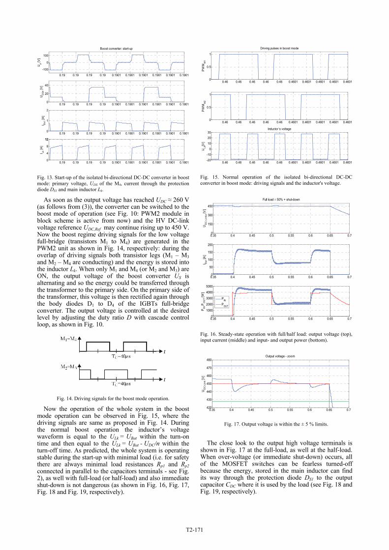
Fig. 13. Start-up of the isolated bi-directional DC-DC converter in boost mode: primary voltage, UDS of the M4, current through the protection diode DS1 and main inductor Lk.
As soon as the output voltage has reached UDC ≈ 260 V (as follows from (3)), the converter can be switched to the boost mode of operation (see Fig. 10: PWM2 module in block scheme is active from now) and the HV DC-link voltage reference UDC,Ref may continue rising up to 450 V. Now the boost regime driving signals for the low voltage full-bridge (transistors M1 to M4) are generated in the PWM2 unit as shown in Fig. 14, respectively: during the overlap of driving signals both transistor legs (M1 – M3 and M2 – M4 are conducting) and the energy is stored into the inductor Lk. When only M1 and M4 (or M2 and M3) are ON, the output voltage of the boost converter US is alternating and so the energy could be transferred through the transformer to the primary side. On the primary side of the transformer, this voltage is then rectified again through the body diodes D1 to D4 of the IGBTs full-bridge converter. The output voltage is controlled at the desired level by adjusting the duty ratio D with cascade control loop, as shown in Fig. 10.
Fig. 14. Driving signals for the boost mode operation.
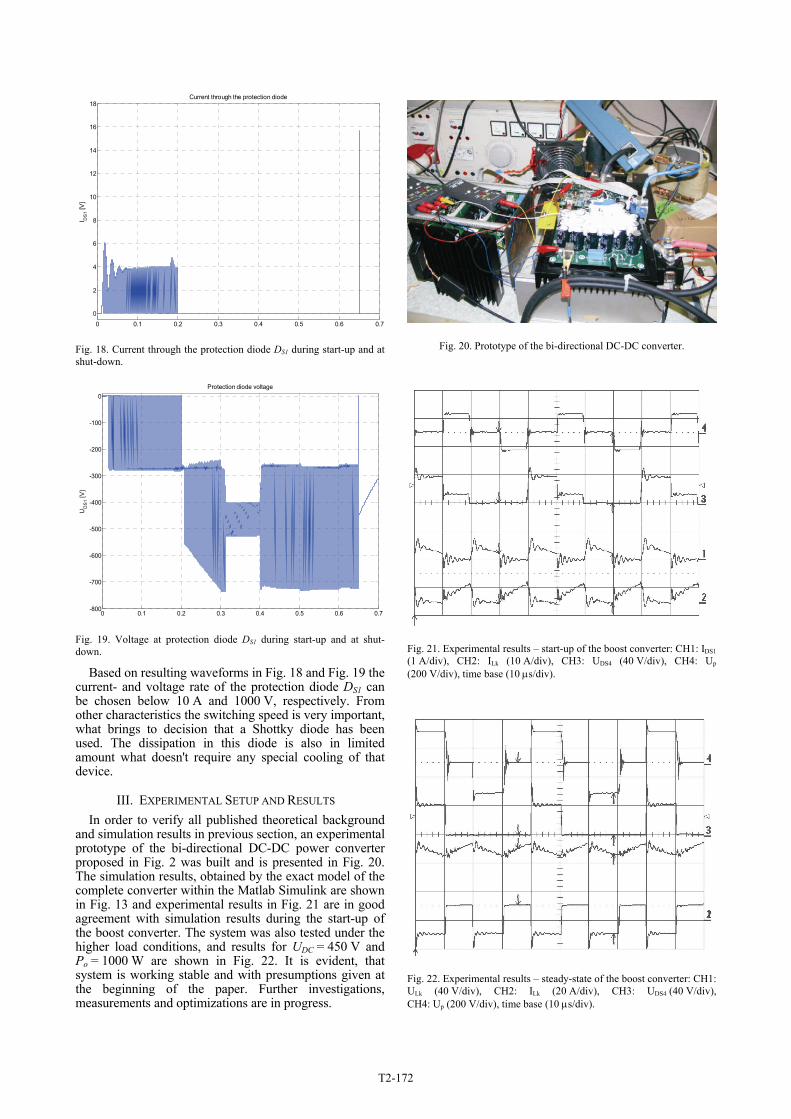
Now the operation of the whole system in the boost mode operation can be observed in Fig. 15, where the driving signals are same as proposed in Fig. 14. During the normal boost operation the inductor’s voltage waveform is equal to the ULk = UBat within the turn-on time and then equal to the ULk = UBat - UDC/n within the turn-off time. As predicted, the whole system is operating stable during the start-up with minimal load (i.e. for safety there are always minimal load resistances Rp1 and Rp2 connected in parallel to the capacitors terminals - see Fig. 2), as well with full-load (or half-load) and also immediate shut-down is not dangerous (as shown in Fig. 16, Fig. 17, Fig. 18 and Fig. 19, respectively).
0.46 0.46 0.46 0.46 0.46 0.4601 0.4601 0.4601 0.4601 0.46010
0.5
1
PW
MM
1
Driving pulses in boost mode
0.46 0.46 0.46 0.46 0.46 0.4601 0.4601 0.4601 0.4601 0.46010
0.5
1
PW
MM
2
0.46 0.46 0.46 0.46 0.46 0.4601 0.4601 0.4601 0.4601 0.4601-20
-10
0
10
20
30
ULk
[V]
Inductor´s voltage
Fig. 15. Normal operation of the isolated bi-directional DC-DC converter in boost mode: driving signals and the inductor's voltage.
0.35 0.4 0.45 0.5 0.55 0.6 0.65 0.70
150
300
450U
DC
-Lin
ka [V
]Full load ± 50% + shut-down
0.35 0.4 0.45 0.5 0.55 0.6 0.65 0.70
50
100
150
200
I Bat
[A]
0.35 0.4 0.45 0.5 0.55 0.6 0.65 0.70
1000
2000
3000
4000
5000
PIN
,PO
UT [W
]
PIN
POUT
Fig. 16. Steady-state operation with full/half load: output voltage (top), input current (middle) and input- and output power (bottom).
0.35 0.4 0.45 0.5 0.55 0.6 0.65 0.7420
430
440
450
460
470
480
UD
C-L
ink [V
]
Output voltage - zoom
Fig. 17. Output voltage is within the ± 5 % limits.
The close look to the output high voltage terminals is
shown in Fig. 17 at the full-load, as well at the half-load. When over-voltage (or immediate shut-down) occurs, all of the MOSFET switches can be fearless turned-off because the energy, stored in the main inductor can find its way through the protection diode DS1 to the output capacitor CDC where it is used by the load (see Fig. 18 and Fig. 19, respectively).
T2-171
0 0.1 0.2 0.3 0.4 0.5 0.6 0.70
2
4
6
8
10
12
14
16
18
I DS
1 [V]
Current through the protection diode
Fig. 18. Current through the protection diode DS1 during start-up and at shut-down.
0 0.1 0.2 0.3 0.4 0.5 0.6 0.7-800
-700
-600
-500
-400
-300
-200
-100
0
UD
S1 [V
]
Protection diode voltage
Fig. 19. Voltage at protection diode DS1 during start-up and at shut-down.
Based on resulting waveforms in Fig. 18 and Fig. 19 the current- and voltage rate of the protection diode DS1 can be chosen below 10 A and 1000 V, respectively. From other characteristics the switching speed is very important, what brings to decision that a Shottky diode has been used. The dissipation in this diode is also in limited amount what doesn't require any special cooling of that device.
III. EXPERIMENTAL SETUP AND RESULTS In order to verify all published theoretical background
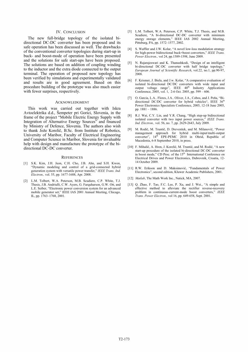
and simulation results in previous section, an experimental prototype of the bi-directional DC-DC power converter proposed in Fig. 2 was built and is presented in Fig. 20. The simulation results, obtained by the exact model of the complete converter within the Matlab Simulink are shown in Fig. 13 and experimental results in Fig. 21 are in good agreement with simulation results during the start-up of the boost converter. The system was also tested under the higher load conditions, and results for UDC = 450 V and Po = 1000 W are shown in Fig. 22. It is evident, that system is working stable and with presumptions given at the beginning of the paper. Further investigations, measurements and optimizations are in progress.
Fig. 20. Prototype of the bi-directional DC-DC converter.
Fig. 21. Experimental results – start-up of the boost converter: CH1: IDS1 (1 A/div), CH2: ILk (10 A/div), CH3: UDS4 (40 V/div), CH4: Up (200 V/div), time base (10 μs/div).
Fig. 22. Experimental results – steady-state of the boost converter: CH1: ULk (40 V/div), CH2: ILk (20 A/div), CH3: UDS4 (40 V/div), CH4: Up (200 V/div), time base (10 μs/div).
T2-172
IV. CONCLUSION The new full-bridge topology of the isolated bi-
directional DC-DC converter has been proposed and its safe operation has been discussed as well. The drawbacks of the conventional converter topologies during start-up in buck- and boost-mode of operation have been presented and the solutions for safe start-ups have been proposed. The solutions are based on addition of coupling winding to the inductor and the extra diode connected to the output terminal. The operation of proposed new topology has been verified by simulations and experimentally validated and results are in good agreement. Based on this procedure building of the prototype was also much easier with fewer surprises, respectively.
ACKNOWLEDGMENT This work was carried out together with Iskra
Avtoelektrika d.d., Šempeter pri Gorici, Slovenia, in the frame of the project “Mobile Electric Energy Supply with Integration of Alternative Energy Sources” and financed by Ministry of Defence, Slovenia. The authors also wish to thank Jože Korelič, B.Sc. from Institute of Robotics, University of Maribor, Faculty of Electrical Engineering and Computer Science in Maribor, Slovenia for invaluable help with design and manufacture the prototype of the bi-directional DC-DC converter.
REFERENCES [1] S.K. Kim, J.H. Jeon, C.H. Cho, J.B. Ahn, and S.H. Kwon,
“Dynamic modeling and control of a grid-connected hybrid generation system with versatile power transfer,” IEEE Trans. Ind. Electron., vol. 55, pp. 1677-1688, Apr. 2008.
[2] L.M. Tolbert, W.A. Peterson, M.B. Scudiere, C.P. White, T.J. Thesis, J.B. Andriulli, C.W. Ayers, G. Farquharson, G.W. Ott, and L.E. Seiber, “Electronic power conversion system for an advanced mobile generator set,” IEEE IAS 2001 Annual Meeting, Chicago, IL, pp. 1763–1768, 2001.
[3] L.M. Tolbert, W.A. Peterson, C.P. White, T.J. Thesis, and M.B. Scudiere, “A bi-directional DC-DC converter with minimum energy storage elements,” IEEE IAS 2002 Annual Meeting, Pittsburg, PA, pp. 1572–1577, 2002.
[4] S. Waffler and J.W. Kolar, “A novel low-loss modulation strategy for high-power bidirectional buck+boost converters,” IEEE Trans. Power Electron., vol 24, pp.1589-1598, June 2009.
[5] N. Rajarajeswari and K. Thanushkodi, “Design of an intelligent bi-directional DC-DC converter with half bridge topology,” European Journal of Scientific Research, vol.22, no.1, pp.90-97, 2008.
[6] F. Krismer, J. Biela, and J.w. Kolar, “A comparative evaluation of isolated bi-directional DC/DC converters with wide input and output voltage range”, IEEE 40th Industry Applications Conference, 2005, vol. 1, 2-6 Oct. 2005, pp. 599 – 606.
[7] O. Garcia, L.A.. Flores, J.A.. Oliver, J.A., Cobos, and J. Peña, “Bi-directional DC/DC converter for hybrid vehicles“, IEEE 36th Power Electronics Specialists Conference, 2005, 12-18 June 2005, pp. 1881 – 1886.
[8] R.J. Wai, C.Y. Lin, and Y.R. Chang, “High step-up bidirectional isolated converter with two input power sources,” IEEE Trans. Ind. Electron., vol. 56, no. 7, pp. 2629-2643, July 2009.
[9] M. Rodič, M. Truntič, D. Drevenšek, and M. Milanovič, “Power management approach for hybrid multi-input/multi-output converter”, 14th EPE-PEMC 2010 in Ohrid, Republic of Macedonia, 6-8 September 2010, in press.
[10] F. Mihalič, A. Hren, J. Korelič, M. Truntič, and M. Rodič, “A new start-up procedure of the isolated bi-directional DC-DC converter in boost mode,” CD Proc. of the 15th International Conference on Electrical Drives and Power Electronics, Dubrovnik, Croatia, 12-14 October 2009.
[11] R.W. Erikson and D. Maksimović, “Fundamentals of Power Electronics”, second edition, Kluwer Academic Publishers, 2001.
[12] Matlab, The Math Work Inc., Natick, MA, 2007.
[13] Q. Zhao, F. Tao, F.C. Lee, P. Xu, and J. Wei., “A simple and effective method to alleviate the rectifier reverse-recovery problem in continuous-current-mode boost converters,” IEEE Trans. Power Electron., vol 16, pp. 649-658, Sept. 2001.
T2-173
Related Documents