DATA SHEET Preliminary specification 2003 Nov 18 INTEGRATED CIRCUITS SAA7724H Car radio digital signal processor

Welcome message from author
This document is posted to help you gain knowledge. Please leave a comment to let me know what you think about it! Share it to your friends and learn new things together.
Transcript

DATA SHEET
Preliminary specification 2003 Nov 18
INTEGRATED CIRCUITS
SAA7724HCar radio digital signal processor

2003 Nov 18 2
Philips Semiconductors Preliminary specification
Car radio digital signal processor SAA7724H
CONTENTS
1 FEATURES
2 GENERAL INFORMATION
2.1 DSP radio system2.2 SAA7724H2.3 Sample rates
3 ORDERING INFORMATION
4 BLOCK DIAGRAM
5 PINNING
6 FUNCTIONAL DESCRIPTION
6.1 Voltage regulator6.2 Audio analog front-end6.2.1 Selector diagram6.2.2 Realization of the common mode input with AIN6.2.3 Realization of the differential ADIFF input6.2.4 Realization of the auxiliary input with volume
control6.2.5 Supplies and references6.3 AD decimation paths (DAD)6.3.1 LDF and AUX decimation path6.3.2 ADF and audio decimation path6.4 Digital audio input/output6.4.1 General6.4.2 External I2S-bus input/output ports6.4.3 External SPDIF input6.4.4 EPICS host I2S-bus port6.5 Sample rate converter6.6 IF_AD6.6.1 IF_AD single block diagram6.6.2 IF_AD detailed functional description6.7 AUDIO_EPICS specific information6.7.1 AUDIO_EPICS start-up6.7.2 AUDIO_EPICS memory overview6.8 SDAC output path6.8.1 DAC upsampling filter6.8.2 DAC noise shaper6.8.3 DAC CoDEM scrambler6.8.4 Multi-bit SDAC6.8.5 Analog summer function6.8.6 SDAC application diagram6.9 Reset block functional overview6.9.1 Asynchronous reset
6.10 Clock circuit and oscillator6.10.1 Circuit description6.10.2 External clock input mode6.10.3 Crystal oscillator supply6.10.4 Application guidelines6.11 PLL circuits6.12 RDS6.12.1 General description6.12.2 RDS I/O modes6.12.3 RDS demodulator6.12.4 RDS bit buffer6.12.5 RDS/RBDS decoder
7 LIMITING VALUES
8 THERMAL RESISTANCE
9 DC CHARACTERISTICS
10 AC CHARACTERISTICS
10.1 Timing diagrams
11 I2C-BUS CONTROL
11.1 I2C-bus protocol11.1.1 Protocol of the I2C-bus commands11.2 MPI data transfer formats11.3 Reset initialization11.4 Defined I2C-bus address11.5 I2C-bus memory map specification
12 I2S-BUS CONTROL
12.1 Basic system requirements12.2 Serial data12.3 Word select
13 PACKAGE OUTLINE
14 SOLDERING
14.1 Introduction to soldering surface mountpackages
14.2 Reflow soldering14.3 Wave soldering14.4 Manual soldering14.5 Suitability of surface mount IC packages for
wave and reflow soldering methods
15 DATA SHEET STATUS
16 DEFINITIONS
17 DISCLAIMERS
18 PURCHASE OF PHILIPS I2C COMPONENTS
2003 Nov 18 3
Philips Semiconductors Preliminary specification
Car radio digital signal processor SAA7724H
1 FEATURES
• AM and FM digitize at IF
• AM and FM narrow-band/IF AGC
• AM and FM IF filtering
• AM and FM adjustable channel detection/variable IF
• IF filter for WX
• AM and FM demodulation
• AM and FM stereo decoding
• AM and FM stereo pilot detection
• FM pilot notch
• AM pilot filter
• FM stereo blend, high blend, high cut, soft muting andde-emphasis
• AM stereo blend, LP filter, high cut and soft muting
• AM and FM noise blanker
• AM and FM gain adjust and calibration (audio)
• FM multipath detection
• FM multipath correction
• Diversity switching
• Radio Data System (RDS) and Radio Broadcast DataSystem (RBDS) demodulation and decoding
• Tape head calibration, equalization, Dolby B and AMS(from analog tape input)
• CD gain adjust, calibration and compression (fromanalog or digital SPDIF/I2S-bus input)
• Parametric equalization
• Volume control
• Bass control
• Treble control
• Balance/fade control
• DC blocking filter
• Dual source select
• Dual playback
• Channel delays
• Analog summer for four channels (through inputsMONO1 and MONO2)
• Audio limiting.
1.1 Sample rates
The SAA7724H runs at a master clock of 43.2 MHz. Audioprocessing runs at a sample rate of
1 fs× 42.1875 kHz 43.2 MHZ1024
--------------------------= =
2003 Nov 18 4
Philips Semiconductors Preliminary specification
Car radio digital signal processor SAA7724H
2 GENERAL INFORMATION
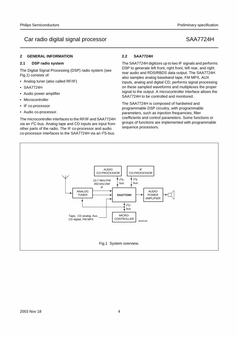
2.1 DSP radio system
The Digital Signal Processing (DSP) radio system (seeFig.1) consists of:
• Analog tuner (also called RF/IF)
• SAA7724H
• Audio power amplifier
• Microcontroller
• IF co-processor
• Audio co-processor.
The microcontroller interfaces to the RF/IF and SAA7724Hvia an I2C-bus. Analog tape and CD inputs are input fromother parts of the radio. The IF co-processor and audioco-processor interfaces to the SAA7724H via an I2S-bus.
2.2 SAA7724H
The SAA7724H digitizes up to two IF signals and performsDSP to generate left front, right front, left rear, and rightrear audio and RDS/RBDS data output. The SAA7724Halso samples analog baseband tape, FM MPX, AUXinputs, analog and digital CD, performs signal processingon these sampled waveforms and multiplexes the propersignal to the output. A microcontroller interface allows theSAA7724H to be controlled and monitored.
The SAA7724H is composed of hardwired andprogrammable DSP circuitry, with programmableparameters, such as injection frequencies, filtercoefficients and control parameters. Some functions orgroups of functions are implemented with programmablesequence processors.
handbook, full pagewidth
MGW194
AUDIOCO-PROCESSOR
IFCO-PROCESSOR
AUDIOPOWER
AMPLIFIER
ANALOGTUNER
10.7 MHz/FM450 kHz/AM
IF
SAA7724H
MICRO-CONTROLLER
Tape, CD analog, Aux,CD digital, FM MPX
I2S-bus
I2C-bus
I2S-bus
Fig.1 System overview.

2003 Nov 18 5
Philips Semiconductors Preliminary specification
Car radio digital signal processor SAA7724H
3 ORDERING INFORMATION
TYPENUMBER
PACKAGE
NAME DESCRIPTION VERSION
SAA7724H QFP100 plastic quad flat package; 100 leads (lead length 1.95 mm);body 14 × 20 × 2.8 mm
SOT317-3
2003 Nov 18 6
Philips Semiconductors Preliminary specification
Car radio digital signal processor SAA7724H
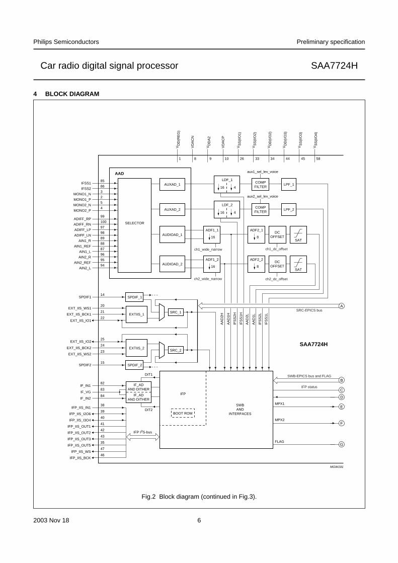
4 BLOCK DIAGRAM
handbook, full pagewidth
MGW191
MPX2
FLAG
MPX1SWBAND
INTERFACES
IFP
BOOT ROM
IFP I2S-bus
SRC_1EXTIIS_1
SPDIF_1
LDF_1
1
16 4COMPFILTER
aux1_sel_lev_voice
LPF_1AUXAD_1
IF_ADAND DITHER
IF_ADAND DITHER
SRC_2
DIT1
DIT2
EXTIIS_2
SPDIF_2
LDF_2
16 4COMPFILTER
aux2_sel_lev_voice
LPF_2AUXAD_2
SELECTOR
85
86
3
2
5
4
99
100
97
98
89
88
87
96
95
94
14
20
21
22
25
24
23
15
82
83
84
38
39
40
41
42
43
35
47
46
AAD
ADF1_1
16AUDIOAD_1
ADF2_1
8DC
OFFSETSAT
ADF1_2
AA
D2H
AA
D1H
IFS
S2H
IFS
S1H
AA
D2L
AA
D1L
IFS
S2L
IFS
S1L
16AUDIOAD_2
ADF2_2
8DC
OFFSETSAT
ch1_wide_narrow
ch2_wide_narrow ch2_dc_offset
ch1_dc_offset
8 9 10 26 33 34 44 45 58
VS
S(I
/O4)
VD
D(R
EG
)
MONO1_P
MONO1_N
MONO2_P
MONO2_N
VD
AC
N
VD
DA
2
VD
AC
P
SPDIF1
SPDIF2
EXT_IIS_WS1
EXT_IIS_BCK1
EXT_IIS_IO1
EXT_IIS_WS2
EXT_IIS_BCK2
EXT_IIS_IO2
VS
S(I
/O1)
VS
S(I
/O2)
VD
D(I
/O2)
IFP_IIS_OUT5
IFP_IIS_IN1
IFP_IIS_I2O6
IFP_IIS_I3O4
IFP_IIS_OUT1
IFP_IIS_OUT2
IFP_IIS_OUT3
VD
D(I
/O3)
VS
S(I
/O3)
IFP_IIS_BCK
IFP_IIS_WS
ADIFF_RN
ADIFF_RP
ADIFF_LN
ADIFF_LP
AIN2_R
AIN2_REF
AIN2_L
AIN1_R
AIN1_REF
AIN1_L
IFSS2
IFSS1
IF_IN2
IF_VG
IF_IN1
SAA7724H
C
B
A
D
E
F
G
SRC-EPICS bus
SWB-EPICS bus and FLAG
IFP status
Fig.2 Block diagram (continued in Fig.3).

2003 Nov 18 7
Philips Semiconductors Preliminary specification
Car radio digital signal processor SAA7724H
handbook, full pagewidth
MGW192
RESETPLL1
OSCILLATORAND CLOCK
RDSDEC_1RDSDEM_1
MPIRDS
sel_rds_clk1_davn2
sel_davn2_rds_flag
50 51 52 53 49 48 13 17 19 18 75 78 77 7616
IFP status
SWB-EPICS bus and LFLAG
SRC-EPICS bus
EPICS I2S-bus
PLL2
AUDIO_EPICS
SRC_EPICS
TCB
IIC_REG
DIO
NOISESHAPER
INTERPOLATORSDAC_FF
R128SDAC_R
AUDIO_EPICS
ch.st. SPDIF_1
ch.st. SPDIF_2
lock SPDIF_1
lock SPDIF_2
RDSDEC_2RDSDEM_2
28
27
29
37
12
11
6
7
36
30
31
32
54
55
56
57
59
60
61
62
63
80
VR
EF
IF
79
VS
S(I
F)
VD
D(O
SC
)
OS
C_O
UT
OS
C_I
N
VS
S(O
SC
)
71
VS
SD
3
70V
DD
D3
69
VS
SD
5
68
VS
SD
2
67
VD
DD
2
66
VS
SD
1
65
VD
DD
1(M
EM
)
64
VS
SD
6
DSP_IO8
DSP_IO7
DSP_IO6
DSP_IO5
DSP_IO4
DSP_IO3
DSP_IO2
DSP_IO1
DSP_IO0
RD
S_D
AT
A1_
DA
VN
1
RD
S_C
LK1_
DA
VN
2
RD
S_D
AT
A2
RRV
LRV
RFV
LFV
A0
RE
SE
T
TS
CA
N
SH
TC
B
IIS_IN1
IIS_IN2
IIS_IN3
IIS_OUT1
IIS_OUT2
IIS_OUT3
IIS_BCK
IIS_WS
SC
L
SD
A
RD
S_C
LK2
93
VR
EF
AD
92
VA
DC
N
91
VA
DC
P
90
VD
DA
1
81
VD
D(I
F)
SAA7724H
RT
CB
G
F
E
D
C
B
A
VOLTAGEREGULATOR
CO
NR
EG
GA
PR
EG
FE
BR
EG
72 7473
MPX2
MPX1
FLAG
Fig.3 Block diagram (continued from Fig.2)

2003 Nov 18 8
Philips Semiconductors Preliminary specification
Car radio digital signal processor SAA7724H
5 PINNING
Table 1 Functional pin description
SYMBOL PIN DESCRIPTION
VDD(REG) 1 supply voltage for 2.5 V regulator circuit and bias for ADCs (3.3 V)
MONO1_P 2 differential positive analog input to AUX_AD2, AUDIOAD_1 and AUDIOAD_2
MONO1_N 3 differential negative analog input to AUX_AD2, AUDIOAD_1 and AUDIOAD_2
MONO2_P 4 differential positive analog input to AUX_AD2, AUDIOAD_1 and AUDIOAD_2
MONO2_N 5 differential negative analog input to AUX_AD2, AUDIOAD_1 and AUDIOAD_2
RRV 6 analog audio voltage output for the right-rear speaker
LRV 7 analog audio voltage output for the left-rear speaker
VDACN 8 negative reference voltage for the SDAC
VDDA2 9 analog supply voltage for the SDAC (2.5 V)
VDACP 10 positive reference voltage for the SDAC
RFV 11 analog audio voltage output for the right-front speaker
LFV 12 analog audio voltage output for the left-front speaker
A0 13 slave subaddress for I2C-bus selection
SPDIF1 14 SPDIF input channel 1 from digital media source
SPDIF2 15 SPDIF input channel 2 from digital media source
RESET 16 reset input (active LOW)
TSCAN 17 scan control
SHTCB 18 shift clock test control block
RTCB 19 asynchronous reset test control block (active LOW)
EXT_IIS_WS1 20 word select input from digital media source 1 (I2S-bus)
EXT_IIS_BCK1 21 bit clock input from digital media source 1 (I2S-bus)
EXT_IIS_IO1 22 data input/output digital media source 1 (I2S-bus)
EXT_IIS_WS2 23 word select input from digital media source 2 (I2S-bus)
EXT_IIS_BCK2 24 bit clock input from digital media source 2 (I2S-bus)
EXT_IIS_IO2 25 data input/output digital media source 2 (I2S-bus)
VSS(I/O1) 26 ground supply 1 for external digital ports
IIS_IN1 27 data channel input 1 (front channels) from external DSP IC (I2S-bus)
IIS_IN2 28 data channel input 2 (rear channels) from external DSP IC (I2S-bus)
IIS_IN3 29 data channel input 3 from external DSP IC (I2S-bus)
IIS_OUT1 30 data channel output 1 for external DSP IC activated by en_host_io (I2S-bus)
IIS_OUT2 31 data channel output 2 to external DSP IC activated by en_host_io (I2S-bus)
IIS_OUT3 32 data channel output 3 to external DSP IC activated by en_host_io (I2S-bus)
VSS(I/O2) 33 ground supply 2 for external digital ports
VDD(I/O2) 34 supply voltage 2 for external digital ports (3.3 V)
IFP_IIS_OUT5 35 IFP data channel output 5 to external DSP IC activated by ifp_iis_en; can alsobe used as 256 × fs clock output enabled by en_256FS (I2S-bus)
IIS_BCK 36 clock output for external DSP IC enabled by en_host_io (I2S-bus)
IIS_WS 37 word select output for external DSP IC enabled by en_host_io (I2S-bus)
IFP_IIS_IN1 38 IFP data channel input 1 from external DSP IC (I2S-bus)

2003 Nov 18 9
Philips Semiconductors Preliminary specification
Car radio digital signal processor SAA7724H
IFP_IIS_I2O6 39 IFP data channel input 2 from external DSP IC or output data channel 6 toexternal DSP IC selected by ifp_iis_io_mode (I2S-bus)
IFP_IIS_I3O4 40 IFP data channel input 3 from external DSP IC or output data channel 4 toexternal DSP IC selected by ifp_iis_io_mode (I2S-bus)
IFP_IIS_OUT1 41 IFP data channel output 1 to external DSP IC activated by ifp_iis_en (I2S-bus)
IFP_IIS_OUT2 42 IFP data channel output 2 to external DSP IC activated by ifp_iis_en (I2S-bus)
IFP_IIS_OUT3 43 IFP data channel output 3 to external DSP IC activated by ifp_iis_en (I2S-bus)
VDD(I/O3) 44 supply voltage 3 for external digital ports (3.3 V)
VSS(I/O3) 45 ground supply 3 for external digital ports
IFP_IIS_BCK 46 IFP output clock for external DSP IC enabled by ifp_iis_en (I2S-bus)
IFP_IIS_WS 47 IFP word select output for external DSP IC enabled by ifp_iis_en (I2S-bus)
SCL 48 serial clock input (I2C-bus)
SDA 49 serial data input/output (I2C-bus)
RDS_CLK2 50 RDS2 bit clock input/output; default input enabled by rds2_clkin
RDS_DATA2 51 RDS2 data output of RDS2 demodulator
RDS_CLK1_DAVN2 52 DAVN2 or RDS1 bit clock input/output; default input enabled by rds1_clkin
RDS_DATA1_DAVN1 53 RDS1 data output of RDS1 demodulator or RDS1 decoder DAVN1
DSP_IO0 54 general purpose input/output for EPICS (F0 of status register)
DSP_IO1 55 general purpose input/output for EPICS (F1 of status register)
DSP_IO2 56 general purpose input/output for EPICS (F2 of status register)
DSP_IO3 57 general purpose input/output for EPICS (F3 of status register)
VSS(I/O4) 58 ground supply 4 for external digital ports
DSP_IO4 59 general purpose input/output for EPICS (F4 of status register)
DSP_IO5 60 general purpose input/output for EPICS (F5 of status register)
DSP_IO6 61 general purpose input/output for EPICS (F6 of status register)
DSP_IO7 62 general purpose input/output for EPICS (F7 of status register)
DSP_IO8 63 general purpose input/output for EPICS (F8 of status register)
VSSD6 64 ground supply for digital circuitry
VDDD1(MEM) 65 digital supply voltage 1 for memories (2.5 V)
VSSD1 66 digital ground supply 1
VDDD2 67 digital supply voltage 2 (2.5 V)
VSSD2 68 digital ground supply 2
VSSD5 69 digital ground supply 5
VDDD3 70 digital supply voltage 3 (2.5 V)
VSSD3 71 digital ground supply 3
CONREG 72 2.5 V regulator control output
FEBREG 73 2.5 V regulator feedback input
GAPREG 74 band gap reference decoupling pin for voltage regulator
VSS(OSC) 75 ground supply for crystal oscillator circuitry
OSC_IN 76 crystal oscillator input: local crystal oscillator sense for gain control or forcedinput in slave mode
SYMBOL PIN DESCRIPTION

2003 Nov 18 10
Philips Semiconductors Preliminary specification
Car radio digital signal processor SAA7724H
OSC_OUT 77 crystal oscillator output: drive output to crystal
VDD(OSC) 78 positive supply voltage for crystal oscillator circuitry
VSS(IF) 79 IF_AD ground supply
VREFIF 80 IF_AD reference voltage output
VDD(IF) 81 IF_AD 2.5 V supply voltage
IF_IN1 82 analog input to IF_AD1 from tuner IF output
IF_VG 83 IF_AD virtual ground
IF_IN2 84 analog input to IF_AD2 from tuner IF output
IFSS1 85 analog IFSS1 input to AUXAD_1
IFSS2 86 analog IFSS2 input to AUXAD_2
AIN1_L 87 analog input 1 to AAD for left input buffer signal
AIN1_REF 88 common reference voltage input for AIN1 input buffer
AIN1_R 89 analog input 1 to AAD for right input buffer signal
VDDA1 90 analog supply voltage 1 for AUXAD and AAD analog circuitry (2.5 V)
VADCP 91 positive reference voltage input for AAD
VADCN 92 ground reference voltage input for AAD
VREFAD 93 common mode reference voltage output for AAD, AUXAD and buffers
AIN2_L 94 analog input 2 to AAD for left input buffer signal
AIN2_REF 95 common reference voltage input for AIN2 input buffer
AIN2_R 96 analog input 2 to AAD for right input buffer signal
ADIFF_LP 97 analog input to AAD for left positive differential signal
ADIFF_LN 98 analog input to AAD for left negative differential signal
ADIFF_RP 99 analog input to AAD for right positive differential signal
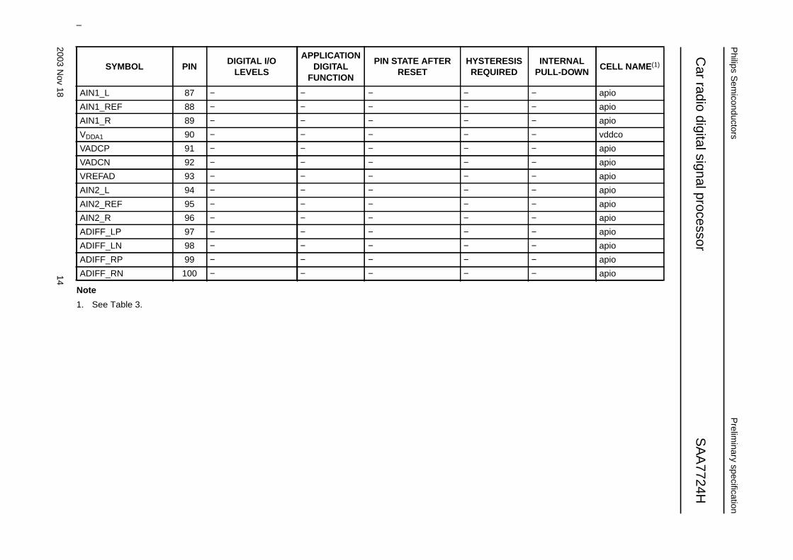
ADIFF_RN 100 analog input to AAD for right negative differential signal
SYMBOL PIN DESCRIPTION

2003N
ov18
11
Philips S
emiconductors
Prelim
inary specification
Car radio digital signal processor
SA
A7724H
This text is here in white to force landscape pages to be rotated correctly when browsing through the pdf in the Acrobat reader.This text is here in_white to force landscape pages to be rotated correctly when browsing through the pdf in the Acrobat reader.This text is here inThis text is here inwhite to force landscape pages to be rotated correctly when browsing through the pdf in the Acrobat reader. white to force landscape pages to be ...
Table 2 Application requirements and padcell type per pin
SYMBOL PINDIGITAL I/O
LEVELS
APPLICATIONDIGITAL
FUNCTION
PIN STATE AFTERRESET
HYSTERESISREQUIRED
INTERNALPULL-DOWN
CELL NAME (1)
VDD(REG) 1 − − − − − vddco
MONO1_P 2 − − − − − apio
MONO1_N 3 − − − − − apio
MONO2_P 4 − − − − − apio
MONO2_N 5 − − − − − apio
RRV 6 − − − − − apio
LRV 7 − − − − − apio
VDACN 8 − − − − − vssco
VDDA2 9 − − − − − vddco
VDACP 10 − − − − − vddco
RFV 11 − − − − − apio
LFV 12 − − − − − apio
A0 13 0 to 5 V DC tolerant input − yes pull-down ipthdt5v
SPDIF1 14 − − − − − apio
SPDIF2 15 − − − − − apio
RESET 16 0 to 5 V DC tolerant input input yes pull-down ipthdt5v
TSCAN 17 0 to 5 V DC tolerant input input yes pull-down ipthdt5v
SHTCB 18 0 to 5 V DC tolerant input input yes pull-down ipthdt5v
RTCB 19 0 to 5 V DC tolerant input input yes pull-down ipthdt5v
EXT_IIS_WS1 20 0 to 5 V DC tolerant input input yes pull-down ipthdt5v
EXT_IIS_BCK1 21 0 to 5 V DC tolerant input input yes pull-down ipthdt5v
EXT_IIS_IO1 22 0 to 5 V DC tolerant bi-directional input yes pull-down bpts10tht5v
EXT_IIS_WS2 23 0 to 5 V DC tolerant input input yes pull-down ipthdt5v
EXT_IIS_BCK2 24 0 to 5 V DC tolerant input input yes pull-down ipthdt5v
EXT_IIS_IO2 25 0 to 5 V DC tolerant bi-directional input yes pull-down bpts10tht5v
VSS(I/O1) 26 − − − − − vsse3v3
IIS_IN1 27 0 to 3.3 V DC input input yes pull-down bpt4mthd
IIS_IN2 28 0 to 3.3 V DC input input yes pull-down bpt4mthd
IIS_IN3 29 0 to 3.3 V DC input input yes pull-down bpt4mthd

2003N
ov18
12
Philips S
emiconductors
Prelim
inary specification
Car radio digital signal processor
SA
A7724H
This text is here in white to force landscape pages to be rotated correctly when browsing through the pdf in the Acrobat reader.This text is here in_white to force landscape pages to be rotated correctly when browsing through the pdf in the Acrobat reader.This text is here inThis text is here inwhite to force landscape pages to be rotated correctly when browsing through the pdf in the Acrobat reader. white to force landscape pages to be ...
IIS_OUT1 30 0 to 3.3 V DC output output and LOW level − − ops10c
IIS_OUT2 31 0 to 3.3 V DC output output and LOW level − − ops10c
IIS_OUT3 32 0 to 3.3 V DC output output and LOW level − − ops10c
VSS(I/O2) 33 − − − − − vsse3v3
VDD(I/O2) 34 − − − − − vdde3v3
IFP_IIS_OUT5 35 0 to 3.3 V DC output output and LOW level − − ops10c
IIS_BCK 36 0 to 3.3 V DC output 3-state − − ot4mc
IIS_WS 37 0 to 3.3 V DC output 3-state − − ots10c
IFP_IIS_IN1 38 0 to 3.3 V DC input input yes pull-down ipthd
IFP_IIS_I2O6 39 0 to 3.3 V DC bi-directional input yes pull-down bpts10thd
IFP_IIS_I3O4 40 0 to 3.3 V DC bi-directional input yes pull-down bpts10thd
IFP_IIS_OUT1 41 0 to 3.3 V DC output output and LOW level − − ops10c
IFP_IIS_OUT2 42 0 to 3.3 V DC output output and LOW level − − ops10c
IFP_IIS_OUT3 43 0 to 3.3 V DC output output and LOW level − − ops10c
VDD(I/O3) 44 − − − − − vdde3v3
VSS(I/O3) 45 − − − − − vsse3v3
IFP_IIS_BCK 46 0 to 3.3 V DC output 3-state − − ot4mc
IFP_IIS_WS 47 0 to 3.3 V DC output 3-state − − ots10c
SCL 48 0 to 5 V DC tolerant input input yes − iptht5v
SDA 49 0 to 5 V DC tolerant bi-directional input − − iic400kt5v
RDS_CLK2 50 0 to 5 V DC tolerant bi-directional input yes − bptons10tht5v
RDS_DATA2 51 0 to 5 V DC tolerant output output mode(level depends onRDS data)
− − bptons10tht5v
RDS_CLK1_DAVN2 52 0 to 5 V DC tolerant bi-directional input yes bptons10tht5v
RDS_DATA1_DAVN1 53 0 to 5 V DC tolerant output output mode(level depends onRDS data)
− − bptons10tht5v
DSP_IO0 54 0 to 5 V DC tolerant bi-directional input yes − bptons10tht5v
DSP_IO1 55 0 to 5 V DC tolerant bi-directional input yes − bptons10tht5v
DSP_IO2 56 0 to 5 V DC tolerant bi-directional input yes − bptons10tht5v
SYMBOL PINDIGITAL I/O
LEVELS
APPLICATIONDIGITAL
FUNCTION
PIN STATE AFTERRESET
HYSTERESISREQUIRED
INTERNALPULL-DOWN
CELL NAME (1)

2003N
ov18
13
Philips S
emiconductors
Prelim
inary specification
Car radio digital signal processor
SA
A7724H
This text is here in white to force landscape pages to be rotated correctly when browsing through the pdf in the Acrobat reader.This text is here in_white to force landscape pages to be rotated correctly when browsing through the pdf in the Acrobat reader.This text is here inThis text is here inwhite to force landscape pages to be rotated correctly when browsing through the pdf in the Acrobat reader. white to force landscape pages to be ...
DSP_IO3 57 0 to 5 V DC tolerant bi-directional input yes − bptons10tht5v
VSS(I/O4) 58 − − − − − vsse3v3
DSP_IO4 59 0 to 5 V DC tolerant bi-directional input yes − bptons10tht5v
DSP_IO5 60 0 to 5 V DC tolerant bi-directional input yes − bptons10tht5v
DSP_IO6 61 0 to 5 V DC tolerant bi-directional input yes − bptons10tht5v
DSP_IO7 62 0 to 5 V DC tolerant bi-directional input yes − bptons10tht5v
DSP_IO8 63 0 to 5 V DC tolerant bi-directional input yes − bptons10tht5v
VSSD6 64 − − − − − vssis
VDDD1(MEM) 65 − − − − − vddco
VSSD1 66 − − − − − vssis
VDDD2 67 − − − − − vddi
VSSD2 68 − − − − − vssis
VSSD5 69 − − − − − vssis
VDDD3 70 − − − − − vddi
VSSD3 71 − − − − − vssis
CONREG 72 − − − − − apio
FEBREG 73 − − − − − apio
GAPREG 74 − − − − − apio
VSS(OSC) 75 − − − − − vssco
OSC_IN 76 − − − − − apio
OSC_OUT 77 − − − − − apio
VDD(OSC) 78 − − − − − vddco
VSS(IF) 79 − − − − − vssco
VREFIF 80 − − − − − apio
VDD(IF) 81 − − − − − vddco
IF_IN1 82 − − − − − aprf
IF_VG 83 − − − − − apio
IF_IN2 84 − − − − − aprf
IFSS1 85 − − − − − apio
IFSS2 86 − − − − − apio
SYMBOL PINDIGITAL I/O
LEVELS
APPLICATIONDIGITAL
FUNCTION
PIN STATE AFTERRESET
HYSTERESISREQUIRED
INTERNALPULL-DOWN
CELL NAME (1)
2003N
ov18
14
Philips S
emiconductors
Prelim
inary specification
Car radio digital signal processor
SA
A7724H
This text is here in white to force landscape pages to be rotated correctly when browsing through the pdf in the Acrobat reader.This text is here in_white to force landscape pages to be rotated correctly when browsing through the pdf in the Acrobat reader.This text is here inThis text is here inwhite to force landscape pages to be rotated correctly when browsing through the pdf in the Acrobat reader. white to force landscape pages to be ...
Note
1. See Table 3.
AIN1_L 87 − − − − − apio
AIN1_REF 88 − − − − − apio
AIN1_R 89 − − − − − apio
VDDA1 90 − − − − − vddco
VADCP 91 − − − − − apio
VADCN 92 − − − − − apio
VREFAD 93 − − − − − apio
AIN2_L 94 − − − − − apio
AIN2_REF 95 − − − − − apio
AIN2_R 96 − − − − − apio
ADIFF_LP 97 − − − − − apio
ADIFF_LN 98 − − − − − apio
ADIFF_RP 99 − − − − − apio
ADIFF_RN 100 − − − − − apio
SYMBOL PINDIGITAL I/O
LEVELS
APPLICATIONDIGITAL
FUNCTION
PIN STATE AFTERRESET
HYSTERESISREQUIRED
INTERNALPULL-DOWN
CELL NAME (1)
2003 Nov 18 15
Philips Semiconductors Preliminary specification
Car radio digital signal processor SAA7724H
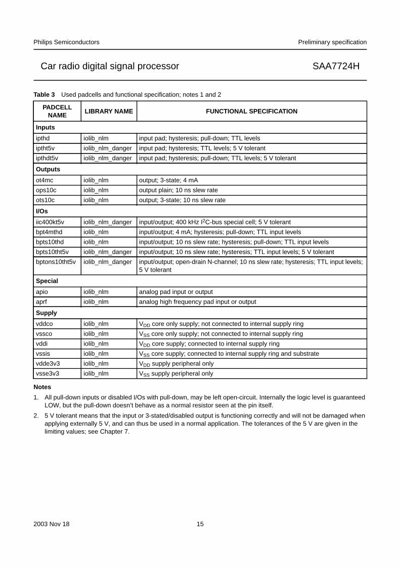
Table 3 Used padcells and functional specification; notes 1 and 2
Notes
1. All pull-down inputs or disabled I/Os with pull-down, may be left open-circuit. Internally the logic level is guaranteedLOW, but the pull-down doesn’t behave as a normal resistor seen at the pin itself.
2. 5 V tolerant means that the input or 3-stated/disabled output is functioning correctly and will not be damaged whenapplying externally 5 V, and can thus be used in a normal application. The tolerances of the 5 V are given in thelimiting values; see Chapter 7.
PADCELLNAME
LIBRARY NAME FUNCTIONAL SPECIFICATION
Inputs
ipthd iolib_nlm input pad; hysteresis; pull-down; TTL levels
iptht5v iolib_nlm_danger input pad; hysteresis; TTL levels; 5 V tolerant
ipthdt5v iolib_nlm_danger input pad; hysteresis; pull-down; TTL levels; 5 V tolerant
Outputs
ot4mc iolib_nlm output; 3-state; 4 mA
ops10c iolib_nlm output plain; 10 ns slew rate
ots10c iolib_nlm output; 3-state; 10 ns slew rate
I/Os
iic400kt5v iolib_nlm_danger input/output; 400 kHz I2C-bus special cell; 5 V tolerant
bpt4mthd iolib_nlm input/output; 4 mA; hysteresis; pull-down; TTL input levels
bpts10thd iolib_nlm input/output; 10 ns slew rate; hysteresis; pull-down; TTL input levels
bpts10tht5v iolib_nlm_danger input/output; 10 ns slew rate; hysteresis; TTL input levels; 5 V tolerant
bptons10tht5v iolib_nlm_danger input/output; open-drain N-channel; 10 ns slew rate; hysteresis; TTL input levels;5 V tolerant
Special
apio iolib_nlm analog pad input or output
aprf iolib_nlm analog high frequency pad input or output
Supply
vddco iolib_nlm VDD core only supply; not connected to internal supply ring
vssco iolib_nlm VSS core only supply; not connected to internal supply ring
vddi iolib_nlm VDD core supply; connected to internal supply ring
vssis iolib_nlm VSS core supply; connected to internal supply ring and substrate
vdde3v3 iolib_nlm VDD supply peripheral only
vsse3v3 iolib_nlm VSS supply peripheral only

2003 Nov 18 16
Philips Semiconductors Preliminary specification
Car radio digital signal processor SAA7724H
handbook, full pagewidth
80
79
78
77
76
75
74
73
72
71
70
69
68
67
66
65
64
63
62
61
60
59
58
57
56
55
54
53
52
51
VREFIF
VSS(IF)VDD(OSC)
OSC_OUT
OSC_IN
VSS(OSC)
GAPREG
FEBREG
CONREG
VSSD3VDDD3VSSD5VSSD2VDDD2VSSD1VDDD1(MEM)VSSD6
DSP_IO8
DSP_IO7
DSP_IO6
DSP_IO5
DSP_IO4
VSS(I/O4)
DSP_IO3
DSP_IO2
DSP_IO1
DSP_IO0
RDS_DATA1_DAVN1
RDS_CLK1_DAVN2
RDS_DATA2
VDD(REG)
MONO1_P
MONO1_N
MONO2_P
MONO2_N
RRV
LRV
VDACN
VDDA2
VDACP
RFV
LFV
A0
SPDIF1
SPDIF2
RESET
TSCAN
SHTCB
RTCB
EXT_IIS_WS1
EXT_IIS_BCK1
EXT_IIS_IO1
EXT_IIS_WS2
EXT_IIS_BCK2
EXT_IIS_IO2
VSS(I/O1)
IIS_IN1
IIS_IN2
IIS_IN3
IIS_OUT1
IIS_O
UT
2
IIS_O
UT
3
VS
S(I
/O2)
VD
D(I
/O2)
IFP
_IIS
_OU
T5
IIS_B
CK
IIS_W
S
IFP
_IIS
_IN
1
IFP
_IIS
_I2O
6
IFP
_IIS
_I3O
4
IFP
_IIS
_OU
T1
IFP
_IIS
_OU
T2
IFP
_IIS
_OU
T3
VD
D(I
/O3)
VS
S(I
/O3)
IFP
_IIS
_BC
K
IFP
_IIS
_WS
SC
L
SD
A
RD
S_C
LK2
AD
IFF
_RN
AD
IFF
_RP
AD
IFF
_LN
AD
IFF
_LP
AIN
2_R
AIN
2_R
EF
AIN
2_L
VR
EF
AD
VA
DC
N
VA
DC
P
VD
DA
1
AIN
1_R
AIN
1_R
EF
AIN
1_L
IFS
S2
IFS
S1
IF_I
N2
IF_V
G
IF_I
N1
VD
D(I
F)
30
29
28
27
26
25
24
23
22
21
20
19
18
17
16
15
14
13
12
11
10
9
8
7
6
5
4
3
2
1
100
99 98 97 96 95 94 93 92 91 90 89 88 87 86 85 84 83 82 81
31 32 33 34 35 36 37 38 39 40 41 42 43 44 45 46 47 48 49 50
MGW193
SAA7724H
Fig.4 Pin configuration.
2003 Nov 18 17
Philips Semiconductors Preliminary specification
Car radio digital signal processor SAA7724H
6 FUNCTIONAL DESCRIPTION
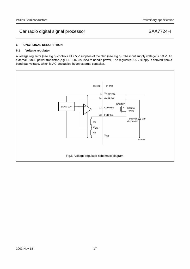
6.1 Voltage regulator
A voltage regulator (see Fig.5) controls all 2.5 V supplies of the chip (see Fig.6). The input supply voltage is 3.3 V. Anexternal PMOS power transistor (e.g. BSH207) is used to handle power. The regulated 2.5 V supply is derived from aband gap voltage, which is AC-decoupled by an external capacitor.
handbook, full pagewidth
MGW195
1 µF
BAND GAPBSH207
externalPMOS
externaldecouplingR1
Vgap
VSS
CONREG
FEBREG
GAPREG
VDD(REG)
R2
on-chip off-chip
72
73
74
1
Fig.5 Voltage regulator schematic diagram.
2003 Nov 18 18
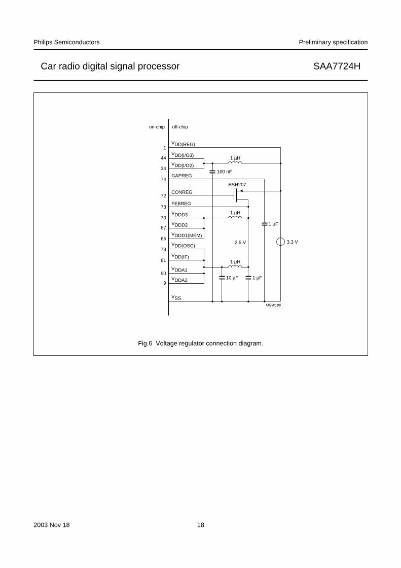
Philips Semiconductors Preliminary specification
Car radio digital signal processor SAA7724H
handbook, full pagewidth
MGW196
1 µH
1 µH
1 µF
1 µF
10 µF
100 nF
3.3 V2.5 V
VSS
VDDD3
VDDD2
VDDD1(MEM)
VDD(OSC)
VDD(IF)
VDDA1
VDDA2
CONREG
FEBREG
GAPREG
VDD(I/O2)
VDD(I/O3)
VDD(REG)
BSH207
1 µH
off-chipon-chip
70
67
65
78
81
90
9
72
73
74
34
44
1
Fig.6 Voltage regulator connection diagram.

2003 Nov 18 19
Philips Semiconductors Preliminary specification
Car radio digital signal processor SAA7724H
6.2 Audio analog front-end
The analog front-end consists of two identical 3rd-order sigma delta stereo ADCs (ADC1 and ADC2) with several inputcontrol blocks for handling common mode signals and acting as input selector (see Fig.7).
handbook, full pagewidth
MGW197
INTREF
CMRR
MONO2_P
VREFAD
AIN1_REF
AIN2_REF
MONO2_N
MONO1_P
IFSS2
IFSS1
MONO1_N
CLKADC1
AUDIOAD_1STEREO
aic1[1:0]
intref1 = 0
refc1
aic2[1:0]
aic3[1:0]
s1
ADF1_2
intref2 = 0
refc2
00
01
10
11
00
01
10
11
00
01
10
11
0
1
s2
0
1
0
1
0
1
1
0
CMRR
AUXAD_2
AUXAD_1
ADIFF_R (P/N)
ADIFF_L (P/N)
2
2
AIN1_R
AIN2_R
AIN1_L
AIN2_L
LEFT2
RIGHT2
CLKAUX
AUXO2
mixc
MIX
AUXO1
AUDIOAD_2STEREO
00
01
10
11
00
01
10
11
0
1
CLKADC2
0
1
0
1
0
1
volmix[1:0] volmix[5:2]
located inSDAC
AAD
SAA7724H
ADF1_1
LEFT1
RIGHT1
86
85
2
3
4
5
95
88
93
97, 98
99, 100
96
89
94
87
Fig.7 Analog front-end switch diagram.
2003 Nov 18 20
Philips Semiconductors Preliminary specification
Car radio digital signal processor SAA7724H
The inputs ADIFF, AIN1, AIN2, MONO1 and MONO2 canbe selected with the audio input controls (aic1 and aic2).The ground reference (REF1 and REF2) can be selected(refc1 and refc2) to enable the handling of common modesignals for AIN1 and AIN2. The switches s1 and s2 areneeded for handling fully differential inputs at the ADIFFpins.
The MONO1 and MONO2 inputs have their own CMRRinput stage and can be redirected to ADC1 and/or ADC2via the audio input control (aic1 and aic2). In this event, theground reference should be switched to internal(intref = 1). It is also possible to pass MONO1/MONO2 to
the AUXAD (controlled by aic3) or directly mix the sameMONO input with four DAC output channels, incorporatingvolume control.
6.2.1 SELECTOR DIAGRAM
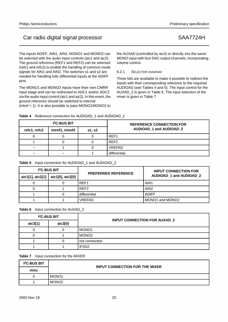
Three bits are available to make it possible to redirect theinputs with their corresponding reference to the requiredAUDIOAD (see Tables 4 and 5). The input control for theAUXAD_2 is given in Table 6. The input selection of themixer is given in Table 7.
Table 4 Reference connection for AUDIOAD_1 and AUDIOAD_2
Table 5 Input connection for AUDIOAD_1 and AUDIOAD_2
Table 6 Input connection for AUXAD_2
Table 7 Input connection for the MIXER
I2C-BUS BIT REFERENCE CONNECTION FORAUDIOAD_1 and AUDIOAD_2refc1, refc2 intref1, intref2 s1, s2
0 0 0 REF1
1 0 0 REF2
− 1 0 VREFAD
− − 1 differential
I2C-BUS BITPREFERRED REFERENCE
INPUT CONNECTION FORAUDIOAD_1 and AUDIOAD_2aic1[1], aic2[1] aic1[0], aic2[0]
0 0 REF1 AIN1
0 1 REF2 AIN2
1 0 differential ADIFF
1 1 VREFAD MONO1 and MONO2
I2C-BUS BITINPUT CONNECTION FOR AUXAD_2
aic3[1] aic3[0]
0 0 MONO1
0 1 MONO2
1 0 not connected
1 1 IFSS2
I2C-BUS BITINPUT CONNECTION FOR THE MIXER
mixc
0 MONO1
1 MONO2
2003 Nov 18 21
Philips Semiconductors Preliminary specification
Car radio digital signal processor SAA7724H
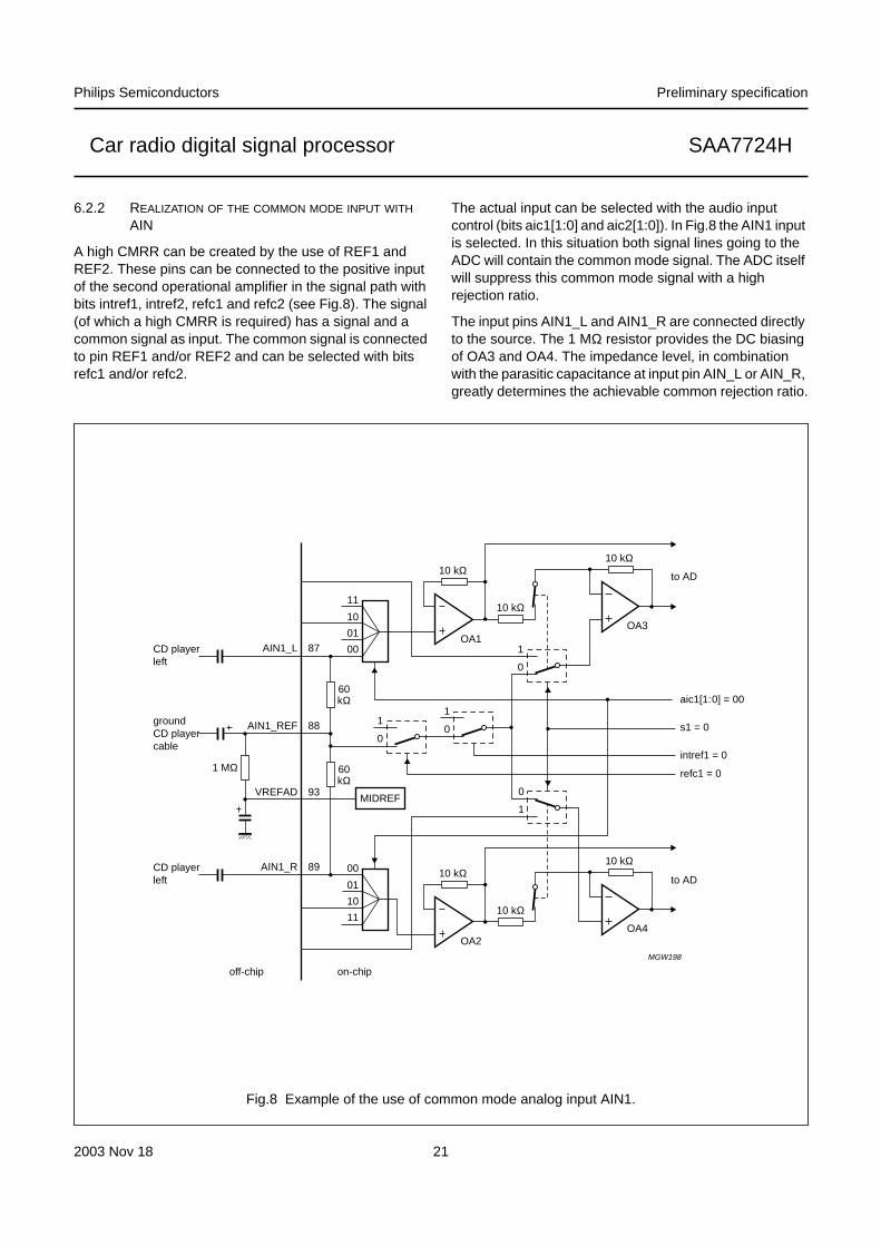
6.2.2 REALIZATION OF THE COMMON MODE INPUT WITH
AIN
A high CMRR can be created by the use of REF1 andREF2. These pins can be connected to the positive inputof the second operational amplifier in the signal path withbits intref1, intref2, refc1 and refc2 (see Fig.8). The signal(of which a high CMRR is required) has a signal and acommon signal as input. The common signal is connectedto pin REF1 and/or REF2 and can be selected with bitsrefc1 and/or refc2.
The actual input can be selected with the audio inputcontrol (bits aic1[1:0] and aic2[1:0]). In Fig.8 the AIN1 inputis selected. In this situation both signal lines going to theADC will contain the common mode signal. The ADC itselfwill suppress this common mode signal with a highrejection ratio.
The input pins AIN1_L and AIN1_R are connected directlyto the source. The 1 MΩ resistor provides the DC biasingof OA3 and OA4. The impedance level, in combinationwith the parasitic capacitance at input pin AIN_L or AIN_R,greatly determines the achievable common rejection ratio.
handbook, full pagewidth
MGW198
60kΩ
60kΩ
1 MΩ
10 kΩ
10 kΩ
AIN1_L
AIN1_R
AIN1_REF
VREFAD
CD playerleft
groundCD playercable
OA1
MIDREF
off-chip on-chip
1
0
10 kΩ
OA3
to AD
aic1[1:0] = 00
s1 = 0
intref1 = 0
refc1 = 0
1
0
0
1
1
0
11
10
01
00
CD playerleft
10 kΩ
10 kΩ
OA2
10 kΩ
OA4
to AD00
01
10
11
87
89
88
93
Fig.8 Example of the use of common mode analog input AIN1.
2003 Nov 18 22
Philips Semiconductors Preliminary specification
Car radio digital signal processor SAA7724H
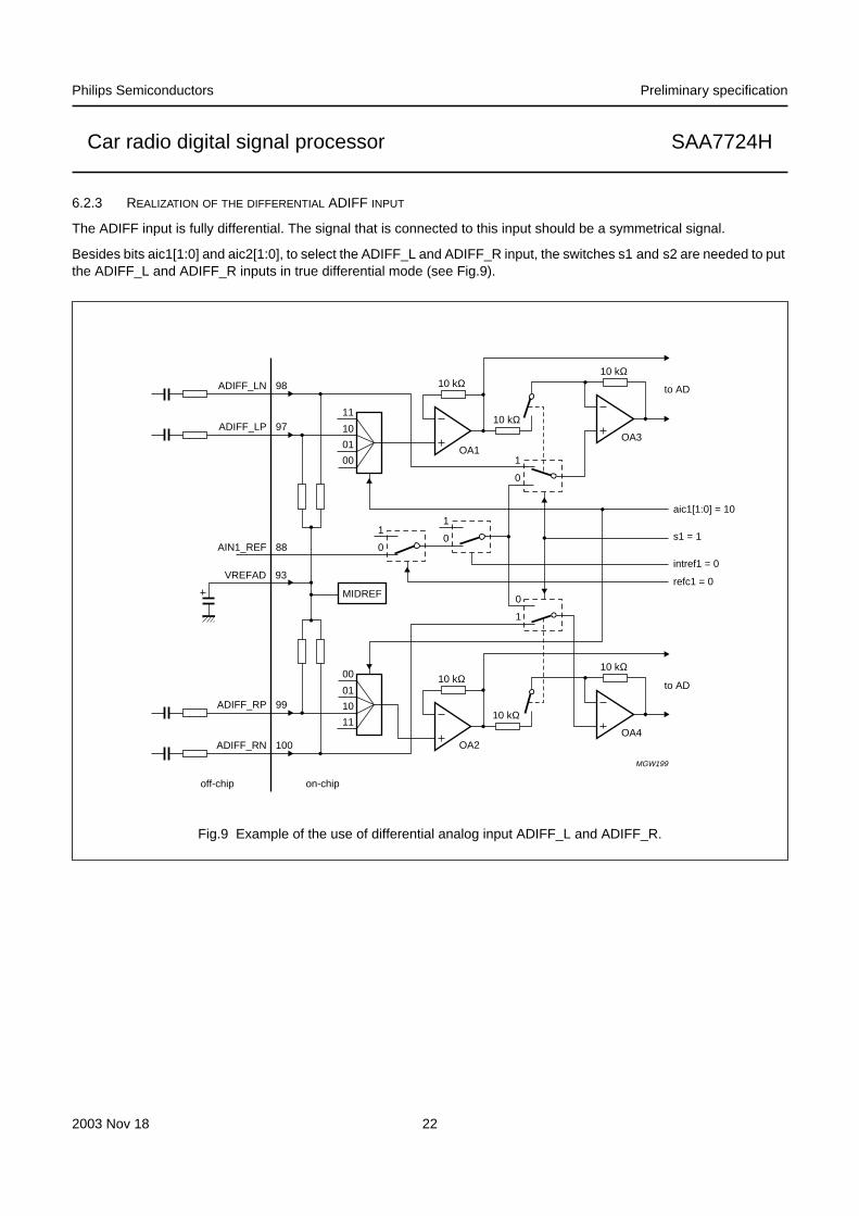
6.2.3 REALIZATION OF THE DIFFERENTIAL ADIFF INPUT
The ADIFF input is fully differential. The signal that is connected to this input should be a symmetrical signal.
Besides bits aic1[1:0] and aic2[1:0], to select the ADIFF_L and ADIFF_R input, the switches s1 and s2 are needed to putthe ADIFF_L and ADIFF_R inputs in true differential mode (see Fig.9).
handbook, full pagewidth
MGW199
10 kΩ
10 kΩ
ADIFF_RP
AIN1_REF
VREFAD
OA1
MIDREF
1
0
10 kΩ
OA3
to AD
aic1[1:0] = 10
s1 = 1
intref1 = 0
refc1 = 0
1
0
0
1
1
0
11
10
01
00
10 kΩ
10 kΩ
OA2
10 kΩ
OA4
to AD00
01
10
11
ADIFF_RN
ADIFF_LP
ADIFF_LN
99
88
93
100
97
98
off-chip on-chip
Fig.9 Example of the use of differential analog input ADIFF_L and ADIFF_R.

2003 Nov 18 23
Philips Semiconductors Preliminary specification
Car radio digital signal processor SAA7724H
6.2.4 REALIZATION OF THE AUXILIARY INPUT WITH VOLUME
CONTROL
A common mode input with volume control for mixing withfour DAC outputs is provided (see Fig.10). The inputsconsist of pins MONO1_P and MONO2_P, bothaccompanied with their ground signals (pins MONO1_Nand MONO2_N). After selection of MONO1 or MONO2,with bit mixc, the volume can be changed from
0 to −22.5 dB in 1.5 dB steps. The attenuated signal canbe added to the left and/or right front and/or left and/or rightrear DAC channels. When the mix signal is added to theoutput, the gain of the output is automatically adjusted toprevent clipping at high input levels.
The inverse output signal of both CMRR circuits can alsobe switched to the AUDIOAD_1 and/or AUDIOAD_2and/or AUXAD_2.
handbook, full pagewidth
MGW200
R = 60 kΩ volmix[5:2]
volmix[5:2]
rlm = 1rrm = 1flm = 1frm = 1
volmix[1:0]
R
AUDIOAD_1 orAUDIOAD_2 or
AUXAD_2
AUDIOAD_1 orAUDIOAD_2 or
AUXAD_2
mixcMidref
MONO1_P
MONO1_N
R
R
R
R
MONO2_P
MONO2_N
VREFAD
R
0
1
R
R
volmix[5:2]
volmix[5:2]
on-chipoff-chip
2
3
4
5
93
Fig.10 MONO input circuit.
Table 8 Mix volume control
The bits volmix[5:2] are binary weighted organized andused for setting the mixer gain from 0 to −18 dB. Theselection bits are connected to the mixer in the QSDAC.
I2C-BUS BITOUTPUT MIX GAIN (dB)
volmix[5:0] (hex)
3F 0
3B −1.5
37 −3.0
33 −4.5
2F −6.0
2B −7.5
27 −9.0
23 −10.5
1F −12.0
1B −13.5
17 −15.0
13 −16.5
0F −18.0
0E −19.5
0D −21.0
0C −22.5
00 MUTE
I2C-BUS BITOUTPUT MIX GAIN (dB)
volmix[5:0] (hex)
2003 Nov 18 24
Philips Semiconductors Preliminary specification
Car radio digital signal processor SAA7724H
The bits volmix[1:0] are also binary weighted organizedand connected to the analog front-end.
The MIX signal can be added to all outputs independant ofeach other.
Table 9 Mix output control; note 1
Note
1. X = not controlled by this bit.
6.2.5 SUPPLIES AND REFERENCES
6.2.5.1 Reference pins VADCN and VADCP
These pins are used as a negative and positive referencefor the AUDIOAD_1 and AUDIOAD_2 and the level ADC.These references needs to be “clean”.
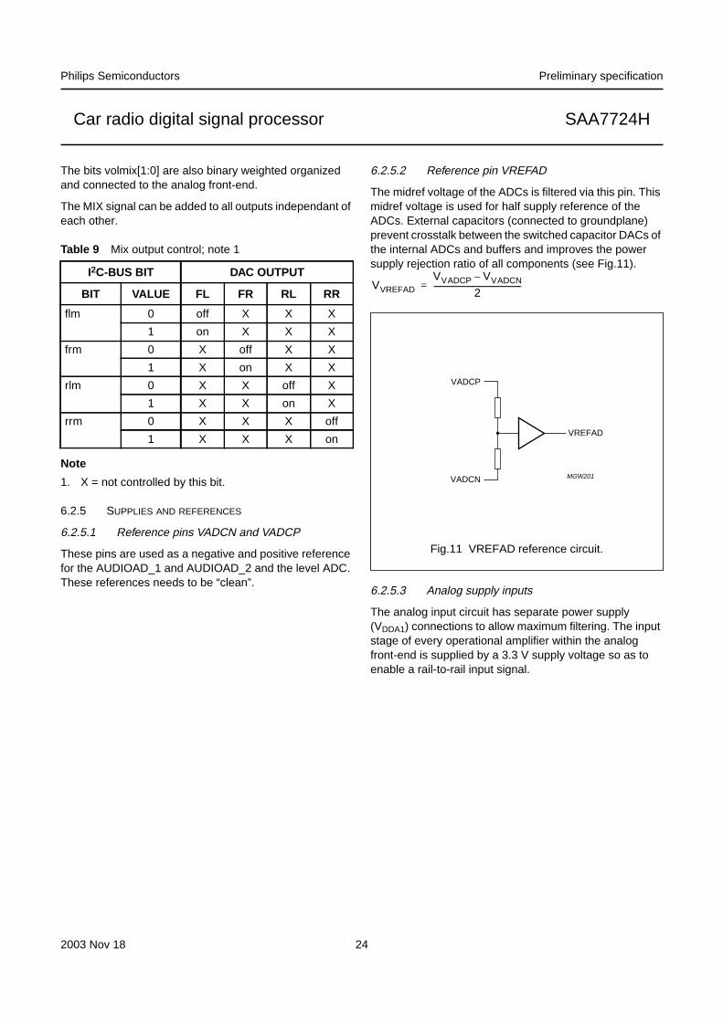
6.2.5.2 Reference pin VREFAD
The midref voltage of the ADCs is filtered via this pin. Thismidref voltage is used for half supply reference of theADCs. External capacitors (connected to groundplane)prevent crosstalk between the switched capacitor DACs ofthe internal ADCs and buffers and improves the powersupply rejection ratio of all components (see Fig.11).
6.2.5.3 Analog supply inputs
The analog input circuit has separate power supply(VDDA1) connections to allow maximum filtering. The inputstage of every operational amplifier within the analogfront-end is supplied by a 3.3 V supply voltage so as toenable a rail-to-rail input signal.
I2C-BUS BIT DAC OUTPUT
BIT VALUE FL FR RL RR
flm 0 off X X X
1 on X X X
frm 0 X off X X
1 X on X X
rlm 0 X X off X
1 X X on X
rrm 0 X X X off
1 X X X on
VVREFAD
VVADCP VVADCN–
2----------------------------------------------=
handbook, halfpage
MGW201
VADCP
VREFAD
VADCN
Fig.11 VREFAD reference circuit.

2003 Nov 18 25
Philips Semiconductors Preliminary specification
Car radio digital signal processor SAA7724H
6.3 AD decimation paths (DAD)
The AD decimation paths for both the level and audio areachieved in the DAD block; (see Fig.12). There are twoDAD blocks implemented for the SAA7724H.
The DAD block consists of a Level Decimation Filter (LDF)which handles the AUX decimation and an AudioDecimation Filter (ADF) which handles the AUDIOdecimation.
handbook, full pagewidth
MGW202
CEADBLOCK
1-BIT CODEFILTER
CEADINTERFACE
CONTROLLER
ADF
LDF
aux(n)_sel_lev_voice
ch(n)_dc_offset
1-BIT CODEFILTER
Fig.12 DAD block diagram.
(n) is 1 or 2.
6.3.1 LDF AND AUX DECIMATION PATH
The input signal has a sample frequency of 128 × fs andcomes from a 1st-order ADC. The first part of thedecimation is done using a CIC filter. For the AUXdecimating filter a 2nd-order CIC filter is implemented.
A branch is also available from this filter for a signal havinga sample frequency of 8 × fs. This signal also passes abuilt-in high-pass filter section to make it adequate for levelIAC detection purposes. With a sampling frequency of8 × 42.1875 kHz the −3 dB point of this filter is atapproximately 60 kHz.
The CIC filter decimates the sample frequency by 64. The
new output sample rate is 2 × fs. The roll-off of the
CIC filter needs to be compensated for, therefore, a roll-offcompensation filter is utilized.
The last stage of the AUX decimation filter is the realizationof the appropriate bandwidth characteristic. The bitsaux1_sel_lev_voice and aux2_sel_lev_voice selects
between the level characteristic and the audiocharacteristic for voice input.
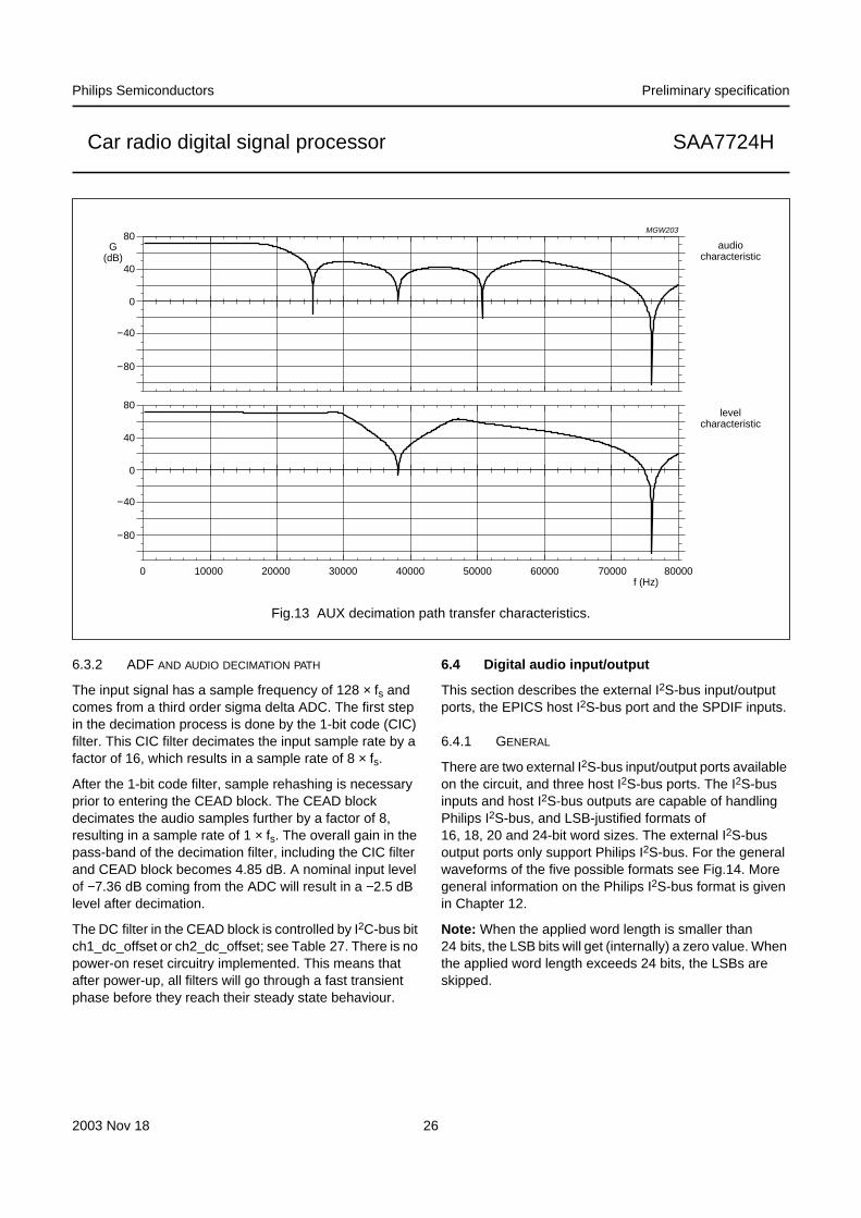
The transfer characteristics, level and audio, of the AUXdecimation filter are illustrated in Fig.13. It should be notedthat the figure corresponds with a 38 kHz sample rate. Forthe SAA7724H a 42.1875 kHz sample rate is used, thehorizontal values need to be scaled with a factor of
Remark : The absolute gain or attenuation of the graphs inFig.13 has no meaning. The relative levels however have.When bit aux1_sel_lev_voice or aux2_sel_lev_voice islogic 1, the coefficient for audio processing is active.When bit aux1_sel_lev_voice or aux2_sel_lev_voice islogic 0, the coefficient for level processing is selected.
xsinx
-----------
42.187538
---------------------
2003 Nov 18 26
Philips Semiconductors Preliminary specification
Car radio digital signal processor SAA7724H
handbook, full pagewidth
MGW203
70000 80000f (Hz)
G(dB)
6000050000400003000020000100000
−80
−40
0
40
80
−80
−40
0
40
80
levelcharacteristic
audiocharacteristic
Fig.13 AUX decimation path transfer characteristics.
6.3.2 ADF AND AUDIO DECIMATION PATH
The input signal has a sample frequency of 128 × fs andcomes from a third order sigma delta ADC. The first stepin the decimation process is done by the 1-bit code (CIC)filter. This CIC filter decimates the input sample rate by afactor of 16, which results in a sample rate of 8 × fs.
After the 1-bit code filter, sample rehashing is necessaryprior to entering the CEAD block. The CEAD blockdecimates the audio samples further by a factor of 8,resulting in a sample rate of 1 × fs. The overall gain in thepass-band of the decimation filter, including the CIC filterand CEAD block becomes 4.85 dB. A nominal input levelof −7.36 dB coming from the ADC will result in a −2.5 dBlevel after decimation.
The DC filter in the CEAD block is controlled by I2C-bus bitch1_dc_offset or ch2_dc_offset; see Table 27. There is nopower-on reset circuitry implemented. This means thatafter power-up, all filters will go through a fast transientphase before they reach their steady state behaviour.
6.4 Digital audio input/output
This section describes the external I2S-bus input/outputports, the EPICS host I2S-bus port and the SPDIF inputs.
6.4.1 GENERAL
There are two external I2S-bus input/output ports availableon the circuit, and three host I2S-bus ports. The I2S-businputs and host I2S-bus outputs are capable of handlingPhilips I2S-bus, and LSB-justified formats of16, 18, 20 and 24-bit word sizes. The external I2S-busoutput ports only support Philips I2S-bus. For the generalwaveforms of the five possible formats see Fig.14. Moregeneral information on the Philips I2S-bus format is givenin Chapter 12.
Note: When the applied word length is smaller than24 bits, the LSB bits will get (internally) a zero value. Whenthe applied word length exceeds 24 bits, the LSBs areskipped.

2003N
ov18
27
Philips S
emiconductors
Prelim
inary specification
Car radio digital signal processor
SA
A7724H
This text is here in white to force landscape pages to be rotated correctly when browsing through the pdf in the Acrobat reader.This text is here in_white to force landscape pages to be rotated correctly when browsing through the pdf in the Acrobat reader.This text is here inThis text is here inwhite to force landscape pages to be rotated correctly when browsing through the pdf in the Acrobat reader. white to force landscape pages to be ...
handbook, full pagewidth
MGW204
16
B5 B6 B7 B8 B9 B10
LEFT
LSB-JUSTIFIED FORMAT 24 BITS
WS
BCK
DATA
RIGHT
1518 1720 1922 212324 2 1
B3 B4MSB B2 B23 LSB
16
B5 B6 B7 B8 B9 B10
1518 1720 1922 212324 2 1
B3 B4MSB B2 B23 LSB
16
MSB B2 B3 B4 B5 B6
LEFT
LSB-JUSTIFIED FORMAT 20 BITS
WS
BCK
DATA
RIGHT
1518 1720 19 2 1
B19 LSB
16
MSB B2 B3 B4 B5 B6
1518 1720 19 2 1
B19 LSB
16
MSB B2 B3 B4
LEFT
LSB-JUSTIFIED FORMAT 18 BITS
WS
BCK
DATA
RIGHT
1518 17 2 1
MSB B2 B3 B4B17 LSB
16 1518 17 2 1
B17 LSB
16
MSB B2
LEFT
LSB-JUSTIFIED FORMAT 16 BITS
WS
BCK
DATA
RIGHT
15 2 1
B15 LSB
16
MSB B2
15 2 1
B15 LSB
MSB MSBB2
21> = 81 2 3
LEFT
INPUT FORMAT I2S-BUS
WS
BCK
DATA
RIGHT
3 > = 8
MSB B2
Fig.14 Waveforms of standardized digital input and output signals.

2003 Nov 18 28
Philips Semiconductors Preliminary specification
Car radio digital signal processor SAA7724H
6.4.2 EXTERNAL I2S-BUS INPUT/OUTPUT PORTS
An I2S-bus interface is provided for communication withexternal digital sources. It is a serial 3-line bus, having oneline for data, one line for clock and one line for the wordselect. For external digital sources the circuit acts as aslave, so the external source is master and supplies the BitClock (BCK) and Word Select (WS).
Figure 15 shows the external I2S-bus receiver andcontrols.
Table 10 defines the possible modes that must be set forthe I2S-bus inputs.
An extra function that is provided is that the EXT_IIS portscan also be set, as an output, from the Sample RateConverters (SRC). In this event only the Philips I2S-busformat is supported.
Table 10 External I2S-bus input formats
Note
1. X = don’t care.
6.4.2.1 SRC audio signal flows
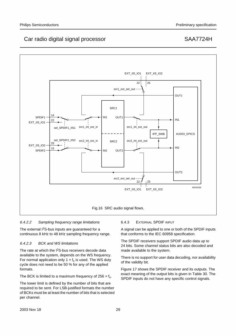
Figure 16 shows the audio signal flow possibilities for thesample rate converters SRC1 and SRC2. The inputs to theSRCs can be either an external source, or an internalsignal from the AUDIO_EPICS.
The outputs from the SRCs can either work as a slaveoutput from an externally connected bus to an externalI2S-bus Port 1 or 2, or it can convert the internalSAA7724H sample rate directly to the AUDIO_EPICS andthe switchboard in the IFP. If conversion to an externalsample rate is selected, the audio signals to the IFPsswitchboard and the AUDIO_EPICS are muted, while theirsample rates are maintained at the internal SAA7724Hsample rate.
All I/O possibilities of the SRCs can be set by eightindependent I2C-bus bits. Some selections are conflictingor make no sense. In order to keep as much flexibility aspossible there is no detection of conflicting settings,however the circuitry is guaranteed not to cause a hang-upsituation.
All audio paths to and from the SRCs are 24 bits wide.Inside the switchboard from the IFP, the audio is alwaystruncated to 16 bits.
ext_host_io_format1 [2:0]ext_host_io_format2 [2:0]
FORMAT
0 X(1) X(1) Philips I2S-bus
1 0 0 LSB -justified 16 bits
1 0 1 LSB-justified 18 bits
1 1 0 LSB-justified 20 bits
1 1 1 LSB-justified 24 bits
handbook, halfpage
MGW205
EXT_IIS_WS(n)
ext_host_io_format(n)[2:0]
to SRC
3
I2S-BUSRECEIVER
EXT_IIS_BCK(n)
EXT_IIS_DATA(n)
Fig.15 External I2S-bus input and controls.
(n) is 1 or 2.
2003 Nov 18 29
Philips Semiconductors Preliminary specification
Car radio digital signal processor SAA7724H
Fig.16 SRC audio signal flows.
handbook, full pagewidth
MGW206
src1_int_ext_insel_SPDIF1_IIS1
src2_int_ext_in
src1_int_ext_out
src1_ext_sel_out
src2_ext_sel_out
src2_int_ext_outsel_SPDIF2_IIS2
SPDIF1 IN1IN1
OUT1
IN2
OUT2
IN2
SRC1
AUDIO_EPICSIFP_SWB
SRC2
OUT2
OUT1
SPDIF2
EXT_IIS_IO1
EXT_IIS_IO1 EXT_IIS_IO2
EXT_IIS_IO1 EXT_IIS_IO2
EXT_IIS_IO2
14
15
22
25
2522
2522
6.4.2.2 Sampling frequency range limitations
The external I2S-bus inputs are guaranteed for acontinuous 8 kHz to 48 kHz sampling frequency range.
6.4.2.3 BCK and WS limitations
The rate at which the I2S-bus receivers decode dataavailable to the system, depends on the WS frequency.For normal application only 1 × fs is used. The WS dutycycle does not need to be 50 % for any of the appliedformats.
The BCK is limited to a maximum frequency of 256 × fs.
The lower limit is defined by the number of bits that arerequired to be sent. For LSB-justified formats the numberof BCKs must be at least the number of bits that is selectedper channel.
6.4.3 EXTERNAL SPDIF INPUT
A signal can be applied to one or both of the SPDIF inputsthat conforms to the IEC 60958 specification.
The SPDIF receivers support SPDIF audio data up to24 bits. Some channel status bits are also decoded andmade available to the system.
There is no support for user data decoding, nor availabilityof the validity bit.
Figure 17 shows the SPDIF receiver and its outputs. Theexact meaning of the output bits is given in Table 30. TheSPDIF inputs do not have any specific control signals.

2003 Nov 18 30
Philips Semiconductors Preliminary specification
Car radio digital signal processor SAA7724H
handbook, full pagewidth
MGW207
SPDIF(n)_contentSPDIF(n)
LOCK
Audio to SRC
SPDIF(n)_emphasis
SPDIF(n)_fs
SPDIF(n)_accuracy
2
2
SPDIFRECEIVER
channelstatus
bits
on chipoff chip
14 or15
Fig.17 SPDIF receiver and its outputs.
(n) is 1 or 2.
6.4.3.1 SPDIF input application diagram
Figure 18 shows the general set-up for an SPDIF input for consumer applications.
Figure 19 shows an example of how to prevent crosstalk from two adjacent SPDIF inputs, due to the parasiticcapacitance from lead finger and bond wires. Therefore extra capacitors are added near the pins.
handbook, halfpage
MGW208
SPDIF input
75 Ω100 pF
100 nF
Fig.18 General SPDIF input application.
handbook, full pagewidth
MGW209
SPDIF1
leadfinger/bondwirecapacitor
75 Ω100 pF 100 pF
100 nF
SPDIF2
75 Ω100 pF 100 pF
100 nF
14
15
Fig.19 Example of crosstalk prevention for SPDIF inputs.
2003 Nov 18 31
Philips Semiconductors Preliminary specification
Car radio digital signal processor SAA7724H
6.4.3.2 Sampling frequency range limitations
The external SPDIF input sample rates are 32, 44.1 and48 kHz.
The accuracies of the supported standardized samplingfrequencies at the SPDIF inputs meets the requirements ofLevel II accuracy as specified in IEC 60958, being 0.1 %.
6.4.3.3 Channel status bits
The channel status bits given in Table 11 are availablefrom the SPDIF receiver. The information is taken from theleft audio channel.
The channel status bits are available in the I2C-bus map,where the exact meaning of the bits can also be found; seeTable 30.
Table 11 SPDIF channel status bits
6.4.3.4 Lock indicator
The SPDIF receiver has a LOCK pin. The polarity isdescribed in the I2C-bus map. When the system is not inlock, the audio data will be muted (being zero data values).In the event that the SPDIF signal is missing or verydistorted, the timing information to the SRC from theSPDIF receiver will not be good or may even disappear.This will cause the SRC to get unlocked.
Locking will occur within 5 ms after reset, or 5 ms after theavailability of a proper SPDIF signal at the input.
The lock indicator is available at one of the EPICS statusflags, and thus also readable via the I2C-bus. The exactlocation is given in Table 25.
6.4.4 EPICS HOST I2S-BUS PORT
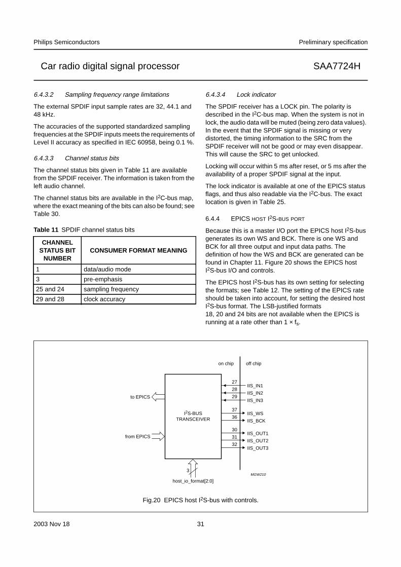
Because this is a master I/O port the EPICS host I2S-busgenerates its own WS and BCK. There is one WS andBCK for all three output and input data paths. Thedefinition of how the WS and BCK are generated can befound in Chapter 11. Figure 20 shows the EPICS hostI2S-bus I/O and controls.
The EPICS host I2S-bus has its own setting for selectingthe formats; see Table 12. The setting of the EPICS rateshould be taken into account, for setting the desired hostI2S-bus format. The LSB-justified formats18, 20 and 24 bits are not available when the EPICS isrunning at a rate other than 1 × fs.
CHANNELSTATUS BIT
NUMBERCONSUMER FORMAT MEANING
1 data/audio mode
3 pre-emphasis
25 and 24 sampling frequency
29 and 28 clock accuracy
handbook, halfpage
3MGW210
host_io_format[2:0]
to EPICS
from EPICS
I2S-BUSTRANSCEIVER
IIS_IN1
IIS_IN2
IIS_IN3
IIS_OUT1
IIS_OUT2
IIS_OUT3
IIS_WS
IIS_BCK
27
28
29
30
31
32
37
36
off chipon chip
Fig.20 EPICS host I2S-bus with controls.
2003 Nov 18 32
Philips Semiconductors Preliminary specification
Car radio digital signal processor SAA7724H
Table 12 External EPICS host I2S-bus formats
Notes
1. X = don’t care.
2. Not supported for EPICS rates other than 1 × fs.
6.5 Sample rate converter
There are two Sample Rate Converters (SRCs) available in the SAA7724H. The input of each SRC can be an externalsource or internal audio from the AUDIO_EPICS. The outputs are fed to the IFPs switchboard and the AUDIO_EPICSor to an external I2S-bus port; see Section 6.4.2.1.
Both SRCs meet the requirements given in Table 13.
Table 13 SRC specification
host_io_format2 host_io_format1 host_io_format0 FORMAT
0 X(1) X(1) Philips I2S-bus
1 0 0 LSB-justified 16 bits
1 0 1 LSB-justified 18 bits; note 2
1 1 0 LSB-justified 20 bits; note 2
1 1 1 LSB-justified 24 bits; note 2
SRC CHARACTERISTIC SPECIFICATION
Input sample rate continuously 8 kHz to 48 kHz; absolute accuracy 0.1 %
Output sample rate continuously 8 kHz to 48 kHz
THD + N ≥ 96 dB at 1 kHz
Overall gain 0 dB
Maximum ripple amplitude (0 to 0.45 fs) 0.1 dB
Stop band suppression (0.55 fs to 1 fs) ≥ 98 dB
Output word width 24 bits
Lock time ≤ 45 ms
Audio during unlocked state muted (zero data)
2003 Nov 18 33
Philips Semiconductors Preliminary specification
Car radio digital signal processor SAA7724H
6.6 IF_AD
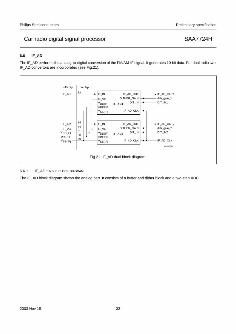
The IF_AD performs the analog-to-digital conversion of the FM/AM-IF signal. It generates 10-bit data. For dual radio twoIF_AD convertors are incorporated (see Fig.21).
handbook, full pagewidth
IF_AD1
IF_IN1 IF_IN IF_AD_OUT
DITHER_GAIN
DIT_IN
IF_AD_OUT1
dith_gain_1
DIT_IN1
IF_AD_CLK
IF_VGVDD(IF)VREFIFVSS(IF)
IF_AD2
IF_IN IF_AD_OUT
DITHER_GAIN
DIT_IN
IF_AD_OUT2
IF_AD_CLK
dith_gain_2
DIT_IN2
IF_AD_CLK
IF_VGVDD(IF)VREFIFVSS(IF)
IF_IN2
IF_VGVDD(IF)VREFIFVSS(IF)
MGW211
82
84
83818079
on chipoff chip
Fig.21 IF_AD dual block diagram.
6.6.1 IF_AD SINGLE BLOCK DIAGRAM
The IF_AD block diagram shows the analog part. It consists of a buffer and dither block and a two-step ADC.
2003 Nov 18 34
Philips Semiconductors Preliminary specification
Car radio digital signal processor SAA7724H
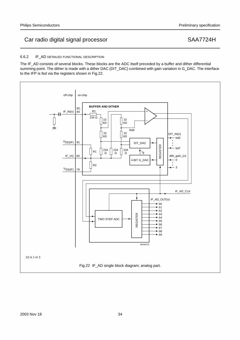
6.6.2 IF_AD DETAILED FUNCTIONAL DESCRIPTION
The IF_AD consists of several blocks. These blocks are the ADC itself preceded by a buffer and dither differentialsumming point. The dither is made with a dither DAC (DIT_DAC) combined with gain variation in G_DAC. The interfaceto the IFP is fed via the registers shown in Fig.22.
handbook, full pagewidth
b0b1b2b3b4b5b6b7b8b9
IF_AD_OUT(n)
IF_AD_CLK
RE
GIS
TE
R
TWO STEP ADC
MGW212
DIT_DAC
DIT_IN(n)
IF_IN(n)
VDD(IF)
VSS(IF)
IF_VG
RE
GIS
TE
R4-BIT G_DAC
R1
R1
BUFFER AND DITHER
Ig
Rdit
bd0
bd7
R2
234Ω
234 Ω
234Ω
234Ω
dith_gain_(n)0
3
10kΩ
10kΩ
10kΩ
10kΩ
off-chip on-chip
82,84
81
79
83
Fig.22 IF_AD single block diagram; analog part.
(n) is 1 or 2.

2003 Nov 18 35
Philips Semiconductors Preliminary specification
Car radio digital signal processor SAA7724H
6.6.2.1 ADC
The ADC is based on the two-step principle.
6.6.2.2 Buffer
The buffer is configured as a single-ended to differentialconvertor.
6.6.2.3 Dithering
Dither can be applied via the dither DACs DIT_DAC andG_DAC. The input voltage range and the dither level areboth proportional to the supply voltage.
DIT_DAC is driven by the IFP. The source is an 8-bit wordhaving 9 values representing −4 (00000000)to +4 (11111111). The total number of 1s in the 8-bit inputword represent the code that the DIT_DAC is using. Themaximum negative output voltage is represented by all 0son the 8-bit word, and the maximum positive outputvoltage is represented by all 1s on the 8-bit word. Anominal value of 0 V, which is half way between themaximum positive output voltage and the maximumnegative output voltage at the output of the DIT_DAC, isrepresented by setting any four of the eight bits to logic 1and the other four bits to logic 0.
To adjust the G_DAC dither to the required level, themultiplying current of the DIT_DAC can be changed with abinary weighted current DAC. The reference current isderived from an internal reference source which isproportional to VDD(IF). As a reference point for theequivalent input dither level, at nominal supply voltage, thefollowing equation is used:
Vditppeq = 3.7 × ditgain (mV).
6.7 AUDIO_EPICS specific information
This chapter contains specific additional information, overthe EPICS7A programmers guide, specifically for theSAA7724H.
The I2C-bus registers, some of which are mapped ontoXMEM address space, are shown in Chapter 11.5,Tables 21 to 23.
6.7.1 AUDIO_EPICS START-UP
The AUDIO_EPICS will start running the code after thereset procedure has been completed. This code will startrunning from address 0 by default, if not reprogrammed bythe user before releasing the pc_reset bit.
6.7.2 AUDIO_EPICS MEMORY OVERVIEW
The memory sizes for the AUDIO_EPICS are given inTable 14.
Table 14 AUDIO_EPICS memory list
6.8 SDAC output path
There are two SDACs implemented in the SAA7724H, onefor the front channels (SDAC_F) and one for the rearchannels (SDAC_R).
The total digital-to-analog conversion path, consists of thefollowing components (see Fig.23):
1. An upsample filter
2. A 3rd-order noise shaper
3. A compensation and dynamic element matching(CoDEM) scrambler
4. The multibit SDAC with current compensation.
All circuitry including the analog part use a 128 × fs clock.
MEMORY TYPE PRODUCT VERSION
DSP program memory ROM: 5120 words
DSP X memory RAM: 3584 words
DSP Y memory RAM: 1024 words
handbook, full pagewidth
MGW213
UPSAMPLE FILTER NOISE SHAPER
1fs 128fs
CODEM
128fs
COMPENSATION
DAC
MULTIBIT DAC
1010
Fig.23 SDAC path diagram.

2003 Nov 18 36
Philips Semiconductors Preliminary specification
Car radio digital signal processor SAA7724H
6.8.1 DAC UPSAMPLING FILTER
The upsampling filter interpolates a 24-bit stereo signalfrom 1 × fs to 8 × fs by cascading two half-band FIR filters.Interpolating to 128 × fs is done by a sample-and-holdfilter.
6.8.2 DAC NOISE SHAPER
A 3rd-order noise shaper is used to quantize the 24-bitinput signal that is fed from the upsampling filter into a 5-bitoutput signal. The generated quantization noise is shapedoutside the audio band.
6.8.3 DAC CODEM SCRAMBLER
The CoDEM scrambler has three different functions.Firstly it converts the 5-bit signal from the noise shaper intoa thermometer code. Secondly, after conversion, thethermometer code is scrambled by means of a Dynamic
Element Matching (DEM) algorithm. Thirdly, by using thiscode, matching errors in the analog part of the SDAC haveless influence on the performance. The CoDEM alsogenerates a compensation vector for the compensationpart of the DAC.
6.8.4 MULTI-BIT SDAC
The SDAC is a multi-bit DAC based upon 31 switchedresistors. The 31 resistors form a network which cancreate 32 DC output levels. The exact analog output levelis the sum of the DC level and the superimposed bitstreamsignal. In the application a simple low-pass filter (onecapacitor) must be used at the outputs of the SDAC.
The overall DAC filters spectral plot is illustrated in Fig.24.
As an example a left filtered output is selected, which alsohas a 3.3 nF output filtering capacitor connected.
handbook, full pagewidth
MGW214
20
filter
100 1 k 10 k 100 k 1 M
α(dB)
3 M−200
−175
−150
−125
−100
−75
−50
−25
0
f (Hz)
left_filtered
Fig.24 DAC filters spectral diagram.
6.8.5 ANALOG SUMMER FUNCTION
The SDAC is featured with the analog summing of signals from the ADCs; for details of this function see Chapter 6.2.
2003 Nov 18 37
Philips Semiconductors Preliminary specification
Car radio digital signal processor SAA7724H
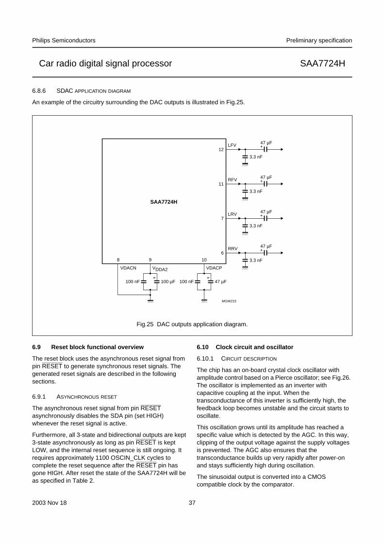
6.8.6 SDAC APPLICATION DIAGRAM
An example of the circuitry surrounding the DAC outputs is illustrated in Fig.25.
handbook, full pagewidth
MGW215
100 µF100 nF 47 µF100 nF
8 9 10
VDACN VDDA2 VDACP
SAA7724H
3.3 nF
RRV6
47 µF
3.3 nF
LRV7
47 µF
3.3 nF
RFV11
47 µF
3.3 nF
LFV12
47 µF
Fig.25 DAC outputs application diagram.
6.9 Reset block functional overview
The reset block uses the asynchronous reset signal frompin RESET to generate synchronous reset signals. Thegenerated reset signals are described in the followingsections.
6.9.1 ASYNCHRONOUS RESET
The asynchronous reset signal from pin RESETasynchronously disables the SDA pin (set HIGH)whenever the reset signal is active.
Furthermore, all 3-state and bidirectional outputs are kept3-state asynchronously as long as pin RESET is keptLOW, and the internal reset sequence is still ongoing. Itrequires approximately 1100 OSCIN_CLK cycles tocomplete the reset sequence after the RESET pin hasgone HIGH. After reset the state of the SAA7724H will beas specified in Table 2.
6.10 Clock circuit and oscillator
6.10.1 CIRCUIT DESCRIPTION
The chip has an on-board crystal clock oscillator withamplitude control based on a Pierce oscillator; see Fig.26.The oscillator is implemented as an inverter withcapacitive coupling at the input. When thetransconductance of this inverter is sufficiently high, thefeedback loop becomes unstable and the circuit starts tooscillate.
This oscillation grows until its amplitude has reached aspecific value which is detected by the AGC. In this way,clipping of the output voltage against the supply voltagesis prevented. The AGC also ensures that thetransconductance builds up very rapidly after power-onand stays sufficiently high during oscillation.
The sinusoidal output is converted into a CMOScompatible clock by the comparator.

2003 Nov 18 38
Philips Semiconductors Preliminary specification
Car radio digital signal processor SAA7724H
handbook, full pagewidth
MGW224
100 kΩ
L12.2 µH
C310 nF
Cx215 pF
Cx115 pF
VDD(OSC) VSS(OSC)
AGC
XTAL1on-chip
off-chip
XTAL2
OSC_IN OSC_OUT
CLKOUT
Gm
Rbias
76 77 78 75
Fig.26 Schematic diagram of the crystal oscillator circuit.
6.10.2 EXTERNAL CLOCK INPUT MODE
It is possible to use the oscillator as a clock input. Inexternal clock input mode, an external clock signal is inputon pin OSC_IN and this clock signal is transferred to theoutput via an extra output inverter stage. In this mode, thequartz crystal, L1, Cx2 and C3 may be removed, but this isnot obligatory.
6.10.3 CRYSTAL OSCILLATOR SUPPLY
The power supply connections to the oscillator areseparated from the other supply lines to minimizefeedback from on-chip ground bounce to the oscillatorcircuit. Noise on the power supply affects the AGCoperation therefore the power supply should bedecoupled. The VSS(OSC) pin is used as ground supply andthe VDD(OSC) as the positive supply.
6.10.4 APPLICATION GUIDELINES
For correct operation of the oscillator, two load capacitors(Cx1 and Cx2) need to be added externally to the chip.This configuration is adequate for the required crystalfrequency of 43.2 MHz.
The external components shown in Fig.26 are specified inTable 15. The use of other values may prevent theoscillator from start-up.
A quartz crystal oscillator is used to generate the clocksignal CLKOUT. In the case of an overtone oscillator, theground harmonic is filtered out by L1 and Cx2.
A quartz crystal should be used with a series resonanceresistance of less than 80 Ω and a capacitance of less than7 pF. The crystal should be manufactured for a loadcapacitance of 10 pF. The value of C3 is not critical as longas it is not much lower than 10 nF (10 % is accurateenough). There is no theoretical upper limit.
Table 15 External components specification for the crystal oscillator
COMPONENT MIN. TYP. MAX. UNIT
Cx1 13.5 15.0 16.5 pF
Cx2 13.5 15.0 16.5 pF
C3 9 10 − nF
L1 1.98 2.2 2.42 µH
2003 Nov 18 39
Philips Semiconductors Preliminary specification
Car radio digital signal processor SAA7724H
6.11 PLL circuits
In the SAA7724H two PLL circuits (PLL1 and PLL2) areavailable that deliver the clocks for the AUDIO_EPICS andthe SRC_EPICS block.
6.12 RDS
In the SAA7724H there are two RDS demodulation anddecoder systems available. The description applies toeach of the RDS blocks.
6.12.1 GENERAL DESCRIPTION
The RDS function recovers the additional inaudible RDSinformation which is transmitted by FM radio broadcasting.The operational functions of the demodulator and decoderare in accordance with EBU specification EN 50067.
The RDS function processes the RDS signal, that isfrequency multiplexed in the stereo-multiplex signal, torecover the information transmitted over the RDS datachannel. This processing consists of band-pass filtering,RDS demodulation and RDS/RBDS decoding.
The stereo-multiplex signal is input from the IFP. Undercontrol of I2C-bus bit rds_clkin, an internal buffer can beused to read out the raw RDS stream in bursts of 16 bits.With the I2C-bus bit rds_clkout the RDS clock can beenabled or switched off. The RDS band signal level can beread from a memory location in the SRC_EPICS, whichneeds to be defined.
The RDS band-pass filter discards the audio content fromthe input signal and reduces the bandwidth.
The RDS band signal level detector removes a possibleAutofahrer Rundfunk Information (ARI) signal from theRDS band-pass filter output and measures the level of theremaining signal.
The RDS demodulator regenerates the raw RDS bitstream(bit rate = 1187.5 Hz) from the modulated RDS signal intwo steps. The first step is the demodulation of the doublesideband suppressed carrier signal around 57 kHz into abaseband signal, by carrier extraction and down-mixing.The second step is the Binary Phase Shift Key (BPSK)demodulation of the biphase coded baseband signal, byclock extraction and correlation.
The RDS/RBDS decoder provides block synchronization,error detection, error correction, complex flywheel functionand programmable block data output. Newly processedRDS/RBDS block information is signalled to the mainmicrocontroller as ‘new data available’ using the DAVNoutput. The block data itself and the corresponding statusinformation can be read out via an I2C-bus request.
The RDS/RBDS decoder contains the following majorfunctions needed for RDS/RBDS data processing:
• RDS and RBDS block detection
• Error detection and correction
• Fast block synchronization
• Synchronization control (flywheel)
• Mode control for RDS/RBDS processing
• Different RDS/RBDS block information output modes(e.g. A/C’ block output mode).
External decoding of the raw RDS bitstream, would requirea microcontroller interrupt every 842 µs. The double 16-bitRDS buffer allows the RDS data to be monitored at a16 times lower rate, i.e. every 13.5 ms.

2003 Nov 18 40
Philips Semiconductors Preliminary specification
Car radio digital signal processor SAA7724H
handbook, full pagewidth
MGW216
RDSBAND-PASS
FILTER
SRC_EPICS
DECODER_BYPASS_MUX
DEMODU-LATOR
0
1
STEREO-MPX
BSLP
BSPA
DA
VN
Out
Mux
RDCL
RDDA
RDS/RBDSDECODER(RBDS+)
BITBUFFER
RDS_BUF_MUX
0 1
rds(n)_clkout
RDS(n)_CLK RDS(n)_DATA
rds(n)_clkin
Fig.27 RDS/RBDS functional block diagram.
(n) is 1 or 2.
6.12.2 RDS I/O MODES
Apart from control inputs and data outputs via the I2C-bus,the following inputs and outputs are related to the RDSfunction.
Unbuffered raw RDS output mode (rds1_clkin = 0,rds2_clkin = 0, rds1_clkout = 1, rds2_clkout = 1 andDAVD mode: dac0 = 1 and dac1 = 1):
• RDS_CLK: clock of the raw RDS bitstream, extractedfrom the biphase coded baseband signal by the RDSdemodulator. A clock period of 1.1875 kHz and 50 %duty cycle. The positive edge can be used to sample theRDS_DATA output.
• RDS_DATA: raw RDS bitstream, generated by thedemodulator detection of a positive going edge on theRDCL input signal. The data output changes every100 µs (this equals 1⁄8 of the RDS_BCK period) after thefalling edge of RDS_BCK. This allows for externalreceivers of the RDS data to clock the data on theRDS_BCK signal as well as on its inverse.
Buffered raw RDS output mode (rds1_clkin = 1,rds2_clkin = 1, rds1_clkout = 0, rds2_clkout = 0 andDAVD mode: dac0 = 1 and dac1 = 1):
• RDS_CLK: burst clock generated by the microcontroller.Bursts of 17 clock cycles are expected. The averagetime between bursts is 13.5 ms.
• RDS_DATA: bursts of 16 raw RDS bits are output undercontrol of the burst clock input. After a data burst, thisoutput is HIGH. It is pulled LOW when 16 new bits aremade available and a new clock burst is expected. Themicrocontroller has to monitor this line at least every13.4 ms.
DAVA, DAVB and DAVC modes (rds1_clkin = 0,rds2_clkin = 0, rds1_clkout = 0 and rds2_clkout = 0):
• DAVN: data available signal for synchronization of datarequest between main controller and decoder; seeSection 6.12.5.11.
rds1_clkin = 1, rds2_clkin = 1, rds1_clkout = 1 andrds2_clkout = 1 is a not allowed mode.
As shown in Fig.27, the same output is used forRDS_DATA and DAVN, depending on the selected mode.
6.12.3 RDS DEMODULATOR
Phase jumps of the extracted RDS clock are detected andaccumulated. If the accumulated phase shift exceeds acertain threshold, the RDS/RBDS decoder is informed bythe bit slip (BSLP) signal. If the RDS/RBDS decoder

2003 Nov 18 41
Philips Semiconductors Preliminary specification
Car radio digital signal processor SAA7724H
detects a bit slip, the RDS demodulator is informed by thebit slip acknowledge (BSPA) signal. This causes theaccumulation of RDS clock phase shifts to be cleared.
6.12.4 RDS BIT BUFFER
The repetition frequency of RDS data is 1187.5 Hz. Thisresults in an interrupt on the microcontroller every 842 µs.The double 16-bit buffer enables this timing requirement tobe relaxed.
The two 16-bit buffers are alternately filled. If a buffer is notread out by the time the other buffer is filled, it will beoverwritten and the old data will be lost.
When a 16-bit buffer is being filled, the RDS bit bufferkeeps the data line HIGH.
If a 16-bit buffer is full, the data line is pulled down. Themicrocontroller has to monitor the data line at least every13.5 ms. The data line remains LOW until themicrocontroller pulls the clock line LOW. This initiates thereading of the buffer and the first bit is output on the dataline. The RDS bit buffer outputs a bit on the data line afterevery falling clock edge. The data is valid when the clockis HIGH. After 16 falling and 16 rising edges, the wholebuffer is read out and the bits are stored by themicrocontroller. After a 17th falling clock edge, the dataline is set HIGH until the other 16-bit buffer is full. Themicrocontroller stops communication by pulling the clockline HIGH again.
6.12.5 RDS/RBDS DECODER
The RDS/RBDS decoder handles the complete dataprocessing and decoding of the continuously receivedserial RDS/RBDS demodulator output data stream (RDDAand RDCL).
Different data processing modes are software controllableby the external main controller via an I2C-bus request. Allcontrol signals are direct inputs to the decoder and arealso available via the I2C-bus.
Processed RDS/RBDS data blocks with correspondingdecoder status information are available via the I2C-bus.The output signals of the decoder are direct outputs andavailable via the I2C-bus.
The RDS/RBDS decoder contains the following functions:
• RBDS processing mode
• RDS/RBDS block detection
• Error detection and correction
• Synchronization
• Flywheel for synchronization hold
• Bit slip correction
• Data processing control
• Restart of synchronization mode
• Error correction control mode for synchronization
• Data available control modes
• Data output of RDS/RBDS information.
The functions which are realized in the decoder aredescribed in detail in the following Sections.
6.12.5.1 RBDS processing mode
The decoder is suitable for receivers intended for theEuropean (RDS) and the USA (RBDS) standard. If theRBDS mode is selected (RBDS = 1) via the I2C-bus, theblock detection and the error detection and correction areadjusted to RBDS data processing; i.e. E blocks are alsotreated as valid blocks. If RBDS is reset to zero then RDSmode is selected.
6.12.5.2 RDS/RBDS block detection
The RDS/RBDS block detection is always active.
For a received sequence of 26 data bits, a valid block andcorresponding offset are identified using syndromecalculation.
During a synchronization search, the syndrome iscalculated with every newly received data bit (bit-by-bit) fora received 26-bit sequence. If the decoder issynchronized, syndrome calculation is activated only after26 data bits for each new block are received.
During RBDS reception, including the RDS blocksequences with (A, B, C/C’ and D) offset, blocksequences of 4 blocks with offset E may also be received.If the decoder detects an ‘E-block’, this block is marked inthe block identification number (BlNr[2:0]) and is availablevia an I2C-bus request. In RBDS processing mode theblock is signalled as valid ‘E-block’ and in RDS processingmode, where only RDS blocks are expected, it is signalledas invalid ‘E-block’.
This information can be used by the main controller todetect ‘E-block’ sequences and identify RDS or RBDStransmitter stations.
6.12.5.3 Error detection and correction
The RDS/RBDS error detection and correction recognizesand corrects transmission errors within a received blockvia parity-check in consideration of the offset word of theexpected block. Burst errors, with a maximum length of5 bits, are corrected using this method; see Table 16.

2003 Nov 18 42
Philips Semiconductors Preliminary specification
Car radio digital signal processor SAA7724H
After synchronization has been detected the errorcorrection is always active, depending on the pre-selected‘error correction mode for synchronization’ (mode SYNCAto SYNCD), but cannot be carried out in every receptionsituation.
During a synchronization search, the error correction isdisabled for detection of the first block and is enabled forprocessing of the second block, depending on thepre-selected error correction mode for synchronization.
The processed block of data and the status of errorcorrection are available for data request, via the I2C-bus,for the last two blocks.
Table 16 RDS processed error correction
Processed blocks are characterized as uncorrectableunder the following conditions:
• During a synchronization search; if the burst error (forthe second block) is higher than allowed by thepre-selected correction mode SYNCA to SYNCD
• After synchronization has been detected; if the bursterror exceeds the correctable maximum 5-bit burst erroror if errors are detected but error correction is notpossible.
6.12.5.4 Synchronization
The decoder is synchronized if two valid blocks in a validsequence are detected by the block detector; seeFigs 8 and 9 for synchronization strategy overview.
The search for the first block is done by a bit-by-bitsyndrome calculation, starting after the first 26 bits havebeen received. This bit-by-bit syndrome calculation iscarried out until the first valid, and error free, block hasbeen received. The next block is then calculated andsyndrome calculation is done after the next 26 bits havebeen received. The block-span in which the second validand expected block can be received is selectable via theprevious setting of the maximum bad blocks gain(RDS2_MBBG[4:0] or RDS1_MBBG[4:0]). If the secondreceived block is an invalid block, then thebad_blocks_counter is incremented and the next newblock is calculated. If the bad_blocks_counter value
reaches the pre-selected max_bad_blocks_gain, then thebit-by-bit search for the first block is restarted.
If the RDS mode is selected then the next block is alwayscalculated from the sequence A-B-C or C’-D, becauseE blocks are not allowed.
If the RBDS mode is selected additional E blocks areallowed. However, while the synchronization search isactive the block sequence E-E is always invalid (nosynchronization will be found with E-E blocks in a row).If the first correctly detected block is block E, then the nextexpected block is block A; in this case no further expectedblocks will be calculated. The decoder waits for an A blockuntil the bad_blocks_counter value reaches thepre-selected max_bad_blocks_gain or a valid A block isreceived.
If the first correct detected block is block D (in RBDSmode) then the next expected block will be block A. If thenext expected block is block A (in RBDS mode) then avalid uncorrected block E is always allowed to besynchronized. If both blocks A and E fail, the nextexpected block calculated is block B and so on.
For the second block, error correction may also beenabled, depending on the pre-selected correction modeSYNCA to SYNCD. Only valid and/or correctable secondblocks are accepted for synchronization.
If the pre-selected max_bad_blocks_gain value is set tozero, then (in this case only) the two-path synchronizationsearch function is active independent of the selected RDSor RBDS mode. That is, if the first block was detected as avalid block, then Path 1 is open and the next expectedblock is calculated and stored.
With each new received bit (bit-by-bit) syndromecalculation is started again until a second valid block isdetected or 26 bits are received.
If a second valid block was detected before 26 bits werereceived, then Path 2 is open, the block position (bitcounter) is stored and the next expected block for Path 2is calculated.
If 26 bits have been received (after the first block Path 1)and the syndrome calculation gives the valid expectedblock for Path 1, then synchronization is detected andPath 2 is ignored.
If 26 bits have been received (after the first block Path 1)and the syndrome calculation gives no validity or it is notthe expected block for Path 1, then Path 1 is set to Path 2values (if Path 2 is active):bit_count_path1 ≤ bit_count_path2 andexpected_block_path1 ≤ expected_block_path2. Path 2 is
EXB1 EXB0 DESCRIPTION
0 0 no errors detected
0 1 burst error of maximum 2 bits corrected
1 0 burst error of maximum 5 bits corrected
1 1 uncorrectable block
2003 Nov 18 43
Philips Semiconductors Preliminary specification
Car radio digital signal processor SAA7724H
then cleared and ready for new input, but only afterreception of the next few bits (until 26) maysynchronization be detected.
Thus using this Path 2 implementation a much fastersynchronization is given in cases of wrong blockinterpretation of the first detected block.
If synchronization is detected, the synchronization statusflag (SYNC) is set and available via an I2C-bus request.The synchronization is held until the bad_blocks_countervalue reaches the pre-selected max_bad_blocks_losevalue (used for synchronization hold) or an external restartof synchronization is performed (NWSY = 1 or Power-onreset).
6.12.5.5 Flywheel for synchronization hold
An internal flywheel is implemented to enable a fastdetection of loss of synchronization. Therefore onecounter (bad_blocks_counter) checks the number ofuncorrectable blocks and a second counter(good_blocks_counter) checks the number of error free orcorrectable blocks. Error blocks increment thebad_blocks_counter value and valid blocks increment thegood_blocks_counter value. If the counter value of thegood_blocks_counter reaches the pre-selectedmax_good_blocks_lose value (MGBL[5:0]) then thegood_blocks_counter and bad_blocks_counters are resetto zero. However, if the bad_blocks_counter valuereaches the pre-selected max_bad_blocks_lose value(MBBL[5:0]) then a new synchronization search (bit-by-bit)is started (SYNC = 0) and both counters are reset to zero.
The flywheel function is only activated if the decoder issynchronized. The synchronization is held until thebad_blocks_counter value reaches the pre-selectedmax_bad_blocks_lose value (loss of synchronization) oran external forced start of a new synchronization search(NWSY = 1) is performed. The maximum values for theflywheel counters are both adjustable via the I2C-bus in arange of 0 to 63.
6.12.5.6 Bit slip correction
During poor reception situations phase shifts of one bit tothe left or right (±1-bit slip) between the RDS/RBDS clockand data may occur, depending on the lock conditions ofthe demodulators clock regeneration.
If the decoder is synchronized and detects a bit slip(BSLP = 1), the synchronization is corrected by +1, 0 or−1 bit via block detection on the respectively shiftedexpected new block.
6.12.5.7 Data processing control
The decoder provides different operating modesselectable by the NWSY, SYM0, SYM1, DAC0 and DAC1inputs via the external I2C-bus. The data processingcontrol performs the pre-selected operating modes andcontrols the requested output of the RDS/RBDSinformation.
6.12.5.8 Restart of synchronization mode
The ‘restart synchronization’ (NWSY) control modeimmediately terminates the actual synchronization andrestarts a new synchronization search procedure(NWSY = 1). The NWSY flag is automatically reset afterthe restart of synchronization by the decoder [NeWSYnchronization Restart (NWSYRe pulse)].
This mode is required for a fast new synchronization on theRDS/RBDS data from a new transmitter station if thetuning frequency is changed by the radio set.
Restart of a synchronization search is automaticallycarried out if the internal flywheel signals a loss ofsynchronization.
6.12.5.9 Error correction control mode forsynchronization
For error correction and identification of valid blocks duringa synchronization search and synchronization hold, fourdifferent modes can be selected by control mode inputsSYM1 and SYM0:
1. Mode SYNCA (SYM1 = 0 and SYM0 = 0): no errorcorrection; the blocks that are detected as correctableare treated as invalid blocks, the internalbad_blocks_counter value is still incremented even ifcorrectable errors are detected. If synchronized, onlyerror free blocks increment the good_blocks_countervalue. All blocks except error free blocks increment thebad_blocks_counter value.
2. Mode SYNCB (SYM1 = 0 and SYM0 = 1): errorcorrection of burst error maximum 2 bits; the blocksthat are corrected are treated as valid blocks, all othererrors detected are treated as invalid blocks. Ifsynchronized, error free and correctable maximum2-bit errors increment the good_blocks_counter value.
3. Mode SYNCC (SYM1 = 1 and SYM0 = 0): errorcorrection of burst error maximum 5 bits; the blocksthat are corrected are treated as valid blocks, all othererrors detected are treated as invalid blocks. Ifsynchronized, error free and correctable maximum5-bit errors increment the good_blocks_counter value.

2003 Nov 18 44
Philips Semiconductors Preliminary specification
Car radio digital signal processor SAA7724H
4. Mode SYNCD (SYM1 = 1 and SYM0 = 1): no errorcorrection; the blocks that are detected as correctableare treated as invalid blocks, if in synchronizationsearch mode. The internal bad_blocks_counter valueis always incremented even if correctable errors aredetected. If synchronized, error free blocks andcorrectable maximum 5-bit errors increment thegood_blocks_counter value. Only uncorrectableblocks increment the bad_blocks_counter value.
6.12.5.10 Data available control modes
The decoder provides three different RDS/RBDS dataoutput processing modes plus one decoder bypass modewhich are selectable via the ‘data available’ control modeinputs DAC1 and DAC0.
• Mode DAVA (DAC1 = 0 and DAC0 = 0): standard outputmode; if the decoder is synchronized and a new block isreceived (every 26 bits), the actual RDS/RBDSinformation of the last two blocks is available with everynew received block (approximately every 21.9 ms).
• Mode DAVB (DAC1 = 0 and DAC0 = 1): fast PI searchmode; during synchronization search and if a newA or C’ block is received, the actual RDS/RBDSinformation of this or the last two A or C’ blocksrespectively is available with every new receivedA or C’ block. If the decoder is synchronized, the‘standard output mode’ is active.
• Mode DAVC (DAC1 = 1 and DAC0 = 0): reduced datarequest output mode; if the decoder is synchronized andtwo new blocks are received (every 52 bits), the actualRDS/RBDS information of the last two blocks isavailable with every two new received blocks(approximately every 43.8 ms).
• Mode DAVD (DAC1 = 1 and DAC0 = 1): decoderbypassed mode; if this mode is selected then theOutMux output of the decoder is reset to LOW(OutMux = 0). The MADRE internal row buffer output isthen active and the decoder is bypassed.
The decoder provides data output of the blockidentification of the last and previously processed blocks,the RDS/RBDS information words and errordetection/correction status of the last two blocks togetherwith general decoder status information.
In addition the decoder output is controlled indirectly by thedata request from the external main controller. Thedecoder receives a ‘data overflow’ (DOFL) signalcontrolled by the I2C-bus register interface.
This DOFL signal has to be set HIGH (DOFL = 1) if thedecoder is synchronized and a new RDS/RBDS block is
received before the previously processed block wascompletely transmitted via the I2C-bus. After detection ofdata overflow the interface registers are not updated (noDecWrE) until reset of the data overflow flag (DOFL = 0)by reading via the I2C-bus or if NWSY = 1 which results inthe start of a new synchronization search (SYNC = 0).
6.12.5.11 Data output of RDS/RBDS information
The decoded RDS/RBDS block information and thecurrent decoder status is available via the I2C-bus. Forsynchronization of data request between the maincontroller and decoder the additional data available output(DAVN) is used. For timing information see Section 10.1.
If the decoder has processed new information for the maincontroller the data available signal (DAVN) is activated(LOW) under the following conditions:
• During a synchronization search in DAVB mode if a validA or C’ block has been detected. This mode can beused for fast search tuning (detection and comparison ofthe PI code contained in the A and C’ blocks).
• During a synchronization search in any DAV mode(except DAVD mode), if two blocks in the correctsequence have been detected (synchronization criterionfulfilled)
• If the decoder is synchronized and, in mode DAVA andDAVB, a new block has been processed; this mode isthe standard data output mode
• If the decoder is synchronized and, in DAVC mode, twonew blocks have been processed
• If the decoder is synchronized and, in any DAV mode(except DAVD mode), loss of synchronization isdetected (flywheel loss of synchronization, resulting in arestart of the synchronization search)
• In any DAV mode (except DAVD mode), if a resetcaused by power-on or a voltage drop is detected(PresN = 0).
Remark : If the decoder is synchronized, the DAVN signalis always activated after 21.9 ms in DAVA or DAVB modeand after 43.8 ms in DAVC mode independent of valid orinvalid blocks being received.
The processed RDS/RBDS data is available for an I2C-busrequest for at least 20 ms after the DAVN signal wasactivated. The DAVN signal is always automaticallydeactivated (HIGH) after ~10 ms or almost after the maincontroller has read the RDS/RBDS status byte via theI2C-bus (see DAVN timing).
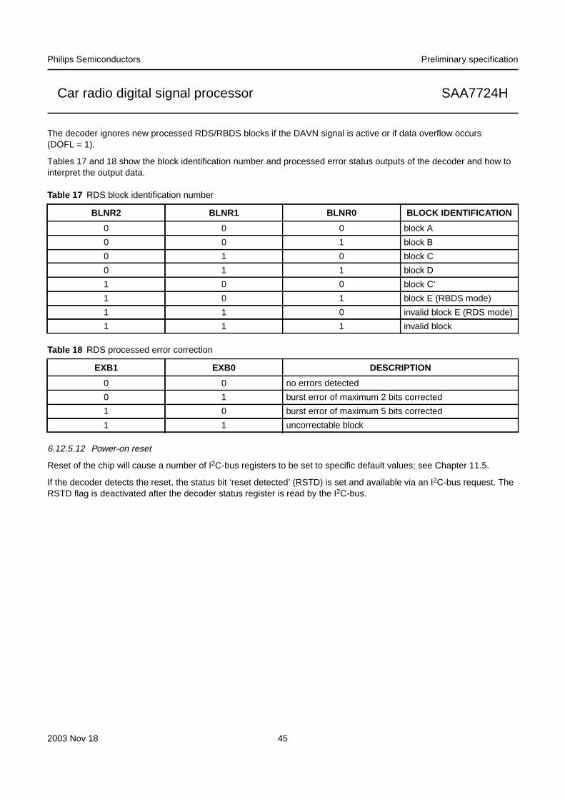
2003 Nov 18 45
Philips Semiconductors Preliminary specification
Car radio digital signal processor SAA7724H
The decoder ignores new processed RDS/RBDS blocks if the DAVN signal is active or if data overflow occurs(DOFL = 1).
Tables 17 and 18 show the block identification number and processed error status outputs of the decoder and how tointerpret the output data.
Table 17 RDS block identification number
Table 18 RDS processed error correction
6.12.5.12 Power-on reset
Reset of the chip will cause a number of I2C-bus registers to be set to specific default values; see Chapter 11.5.
If the decoder detects the reset, the status bit ‘reset detected’ (RSTD) is set and available via an I2C-bus request. TheRSTD flag is deactivated after the decoder status register is read by the I2C-bus.
BLNR2 BLNR1 BLNR0 BLOCK IDENTIFICATION
0 0 0 block A
0 0 1 block B
0 1 0 block C
0 1 1 block D
1 0 0 block C’
1 0 1 block E (RBDS mode)
1 1 0 invalid block E (RDS mode)
1 1 1 invalid block
EXB1 EXB0 DESCRIPTION
0 0 no errors detected
0 1 burst error of maximum 2 bits corrected
1 0 burst error of maximum 5 bits corrected
1 1 uncorrectable block

2003 Nov 18 46
Philips Semiconductors Preliminary specification
Car radio digital signal processor SAA7724H
7 LIMITING VALUESIn accordance with the Absolute Maximum Rating System (IEC 60134); note 1
Notes
1. Stresses greater than those listed above may cause permanent damage to the device. This is a stress rating onlyand functional operation of the device at these or at any other condition above those listed in the followingrecommended operating and characteristics section is not implied. Exposure to absolute maximum rating conditionsfor extended periods of time may affect device reliability.
2. Not applicable for 5 V tolerant pins.
8 THERMAL RESISTANCE
SYMBOL PARAMETER CONDITIONS MIN. TYP. MAX. UNIT
VDDD supply voltage on pin VDDD −0.5 +2.5 +3.3 V
VDD(I/O) supply voltage on pin VDD(I/O) −0.5 +3.3 +4.2 V
VDD(REG) supply voltage on pin VDD(REG) −0.5 +3.3 +4.2 V
VDDA supply voltage on pin VDDA −0.5 +2.5 +3.3 V
IDDD supply current pin VDDD fc = 43.2 MHz; VDDD = 2.5 V − − 750 mA
ISSD supply current pin VSSD fc = 43.2 MHz; VDDD = 2.5 V − − 750 mA
IDD(I/O) supply current pin VDD(I/O) fc = 43.2 MHz; VDDD = 3.3 V − − 750 mA
ISS(I/O) supply current pin VSS(I/O) fc = 43.2 MHz; VDDD = 3.3 V − − 750 mA
IIK DC input clamp diode current VIL < −0.5 V orVIH > VDD(I/O) + 0.5 V; note 2
− − 10 mA
Vlim(5V) 5 V tolerant pins voltage limits 5 V tolerant outputs: disabledmode
−0.5 − +5.8 V
Tamb ambient temperature −40 − +85 °CTstg storage temperature −55 − +150 °CVesd electrostatic discharge voltage HBM: 100 pF; 1500 Ω 2000 − − V
MM: 200 pF; 2.5 µH; 15 Ω 200 − − V
Ilu(prot) latch-up protection current GQS (SNW-FQ-611 part E) 100 − − mA
SYMBOL PARAMETER CONDITION VALUE UNIT
Rth(j-a) thermal resistance from junction toambient
in free air 45 K/W

2003 Nov 18 47
Philips Semiconductors Preliminary specification
Car radio digital signal processor SAA7724H
9 DC CHARACTERISTICSPositive current flows into the device; 3.13 V ≤ VDD(I/O), VDD(REG) ≤ 3.47 V;2.38 V ≤ VDDA, VDDD, VDD(OSC), VDD(IF) ≤ 2.62 V; Tamb = −40 °C to +85 °C.
SYMBOL PARAMETER CONDITIONS MIN. TYP. MAX. UNIT
Digital parameters
VDDD supply voltage on pin VDDD 2.38 2.5 2.62 V
VDD(OSC) supply voltage on pin VDD(OSC) 2.38 2.5 2.62 V
VDD(I/O) supply voltage on pin VDD(I/O) 3.13 3.3 3.47 V
VDD(REG) supply voltage on pin VDD(REG) 3.13 3.3 3.47 V
IDD(tot) total supply current fosc_in = 43.2 MHz
pins VDDD − 215 260 mA
pins VDD(I/O) − 5 10 mA
pins VDDA1, VDDA2, VDD(IF),VDD(OSC)
− 180 216 mA
VIH HIGH-level input voltage VDD(I/O) = 3.3 V; inputs TTL;excluding 5 V tolerant pins
1.7 − 3.3 V
VDD(I/O) = 3.3 V; 5 V tolerantinputs TTL; including SDA pin
2.0 − 5.5 V
VIL LOW-level input voltage inputs TTL; excluding SDA pin 0 − 0.7 V
5 V tolerant inputs TTL;including SDA pin
0 − 0.8 V
VOH HIGH-level output voltage IOH = −4 mA; VDD(I/O) = 3.3 V
10 ns slew rate outputs 2.9 − − V
4 mA outputs 2.9 − − V
VOL LOW-level output voltage 10 ns slew rate outputs;IOL = 4 mA; VDD(I/O) = 3.3 V
− − 0.4 V
4 mA outputs; IOL = 4 mA − − 0.4 V
SDA output; IOL = 3 mA;VDD(I/O) = 3.3 V
− − 0.4 V
ILI input leakage current Schmitt trigger input withoutpull-down; excluding 5 Vtolerant pins
VI = VSS(I/O) − − −1 µA
VI = VDD(I/O) − − 1 µA
Schmitt trigger input withoutpull-down; 5 V tolerant pins only
VI = 5 V − − 4.5 µA
VI = 0 V − − −4.5 µA
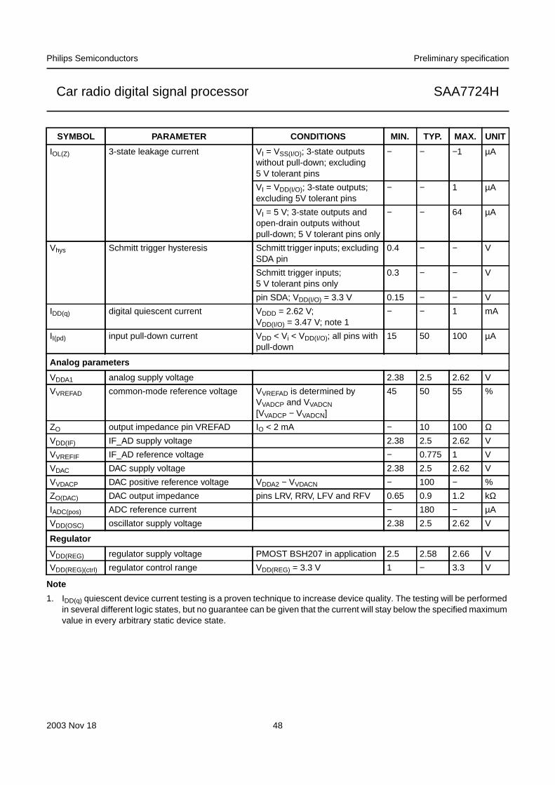
2003 Nov 18 48
Philips Semiconductors Preliminary specification
Car radio digital signal processor SAA7724H
Note
1. IDD(q) quiescent device current testing is a proven technique to increase device quality. The testing will be performedin several different logic states, but no guarantee can be given that the current will stay below the specified maximumvalue in every arbitrary static device state.
IOL(Z) 3-state leakage current VI = VSS(I/O); 3-state outputswithout pull-down; excluding5 V tolerant pins
− − −1 µA
VI = VDD(I/O); 3-state outputs;excluding 5V tolerant pins
− − 1 µA
VI = 5 V; 3-state outputs andopen-drain outputs withoutpull-down; 5 V tolerant pins only
− − 64 µA
Vhys Schmitt trigger hysteresis Schmitt trigger inputs; excludingSDA pin
0.4 − − V
Schmitt trigger inputs;5 V tolerant pins only
0.3 − − V
pin SDA; VDD(I/O) = 3.3 V 0.15 − − V
IDD(q) digital quiescent current VDDD = 2.62 V;VDD(I/O) = 3.47 V; note 1
− − 1 mA
II(pd) input pull-down current VDD < Vi < VDD(I/O); all pins withpull-down
15 50 100 µA
Analog parameters
VDDA1 analog supply voltage 2.38 2.5 2.62 V
VVREFAD common-mode reference voltage VVREFAD is determined byVVADCP and VVADCN[VVADCP − VVADCN]
45 50 55 %
ZO output impedance pin VREFAD IO < 2 mA − 10 100 ΩVDD(IF) IF_AD supply voltage 2.38 2.5 2.62 V
VVREFIF IF_AD reference voltage − 0.775 1 V
VDAC DAC supply voltage 2.38 2.5 2.62 V
VVDACP DAC positive reference voltage VDDA2 − VVDACN − 100 − %
ZO(DAC) DAC output impedance pins LRV, RRV, LFV and RFV 0.65 0.9 1.2 kΩIADC(pos) ADC reference current − 180 − µA
VDD(OSC) oscillator supply voltage 2.38 2.5 2.62 V
Regulator
VDD(REG) regulator supply voltage PMOST BSH207 in application 2.5 2.58 2.66 V
VDD(REG)(ctrl) regulator control range VDD(REG) = 3.3 V 1 − 3.3 V
SYMBOL PARAMETER CONDITIONS MIN. TYP. MAX. UNIT
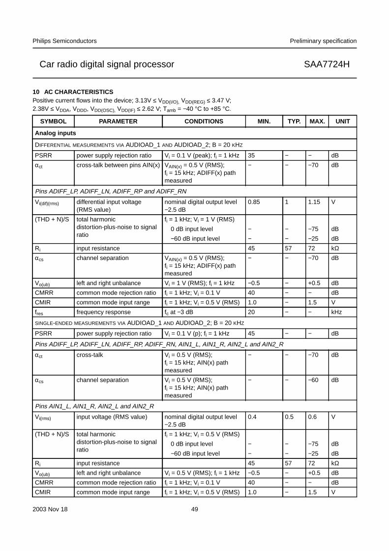
2003 Nov 18 49
Philips Semiconductors Preliminary specification
Car radio digital signal processor SAA7724H
10 AC CHARACTERISTICSPositive current flows into the device; 3.13V ≤ VDD(I/O), VDD(REG) ≤ 3.47 V;2.38V ≤ VDDA, VDDD, VDD(OSC), VDD(IF) ≤ 2.62 V; Tamb = −40 °C to +85 °C.
SYMBOL PARAMETER CONDITIONS MIN. TYP. MAX. UNIT
Analog inputs
DIFFERENTIAL MEASUREMENTS VIA AUDIOAD_1 AND AUDIOAD_2; B = 20 KHZ
PSRR power supply rejection ratio Vi = 0.1 V (peak); fi = 1 kHz 35 − − dB
αct cross-talk between pins AIN(x) VAIN(x) = 0.5 V (RMS);fi = 15 kHz; ADIFF(x) pathmeasured
− − −70 dB
Pins ADIFF_LP, ADIFF_LN, ADIFF_RP and ADIFF_RN
Vi(dif)(rms) differential input voltage(RMS value)
nominal digital output level−2.5 dB
0.85 1 1.15 V
(THD + N)/S total harmonicdistortion-plus-noise to signalratio
fi = 1 kHz; Vi = 1 V (RMS)
0 dB input level − − −75 dB
−60 dB input level − − −25 dB
Ri input resistance 45 57 72 kΩαcs channel separation VAIN(x) = 0.5 V (RMS);
fi = 15 kHz; ADIFF(x) pathmeasured
− − −70 dB
Vo(ub) left and right unbalance Vi = 1 V (RMS); fi = 1 kHz −0.5 − +0.5 dB
CMRR common mode rejection ratio fi = 1 kHz; Vi = 0.1 V 40 − − dB
CMIR common mode input range fi = 1 kHz; Vi = 0.5 V (RMS) 1.0 − 1.5 V
fres frequency response fc at −3 dB 20 − − kHz
SINGLE-ENDED MEASUREMENTS VIA AUDIOAD_1 AND AUDIOAD_2; B = 20 KHZ
PSRR power supply rejection ratio Vi = 0.1 V (p); fi = 1 kHz 45 − − dB
Pins ADIFF_LP, ADIFF_LN, ADIFF_RP, ADIFF_RN, AIN1_L, AIN1_R, AIN2_L and AIN2_R
αct cross-talk Vi = 0.5 V (RMS);fi = 15 kHz; AIN(x) pathmeasured
− − −70 dB
αcs channel separation Vi = 0.5 V (RMS);fi = 15 kHz; AIN(x) pathmeasured
− − −60 dB
Pins AIN1_L, AIN1_R, AIN2_L and AIN2_R
Vi(rms) input voltage (RMS value) nominal digital output level−2.5 dB
0.4 0.5 0.6 V
(THD + N)/S total harmonicdistortion-plus-noise to signalratio
fi = 1 kHz; Vi = 0.5 V (RMS)
0 dB input level − − −75 dB
−60 dB input level − − −25 dB
Ri input resistance 45 57 72 kΩVo(ub) left and right unbalance Vi = 0.5 V (RMS); fi = 1 kHz −0.5 − +0.5 dB
CMRR common mode rejection ratio fi = 1 kHz; Vi = 0.1 V 40 − − dB
CMIR common mode input range fi = 1 kHz; Vi = 0.5 V (RMS) 1.0 − 1.5 V
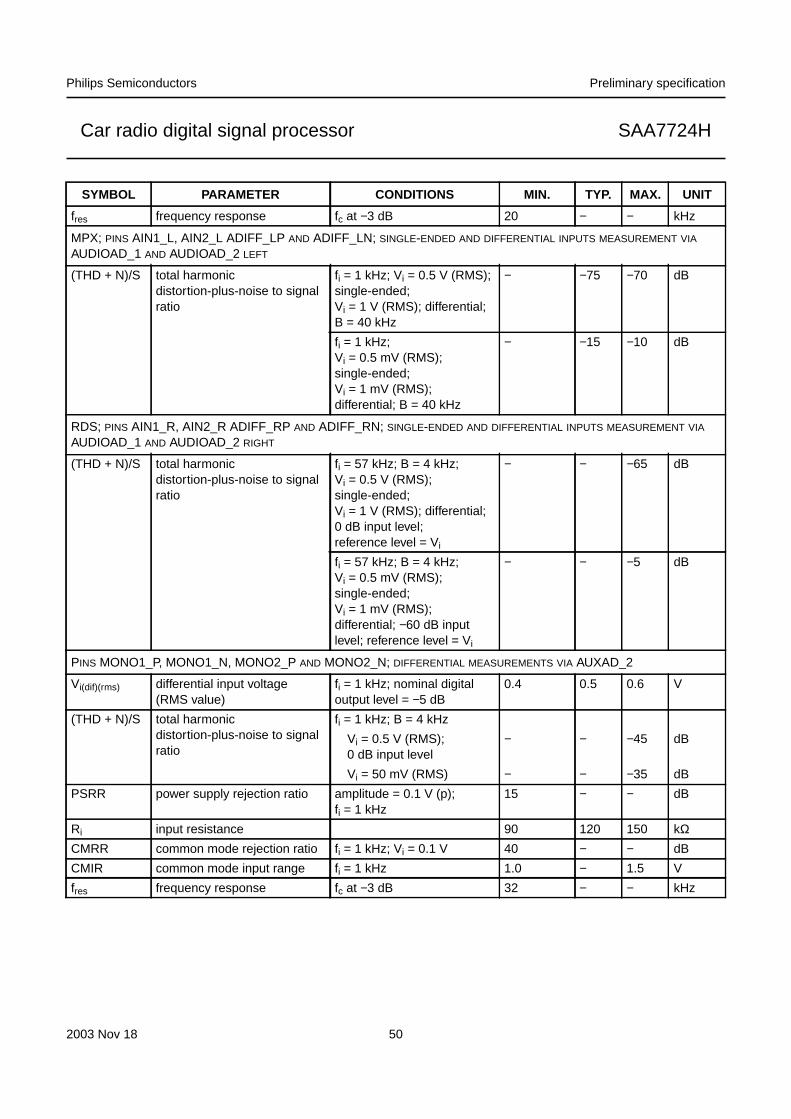
2003 Nov 18 50
Philips Semiconductors Preliminary specification
Car radio digital signal processor SAA7724H
fres frequency response fc at −3 dB 20 − − kHz
MPX; PINS AIN1_L, AIN2_L ADIFF_LP AND ADIFF_LN; SINGLE-ENDED AND DIFFERENTIAL INPUTS MEASUREMENT VIA
AUDIOAD_1 AND AUDIOAD_2 LEFT
(THD + N)/S total harmonicdistortion-plus-noise to signalratio
fi = 1 kHz; Vi = 0.5 V (RMS);single-ended;Vi = 1 V (RMS); differential;B = 40 kHz
− −75 −70 dB
fi = 1 kHz;Vi = 0.5 mV (RMS);single-ended;Vi = 1 mV (RMS);differential; B = 40 kHz
− −15 −10 dB
RDS; PINS AIN1_R, AIN2_R ADIFF_RP AND ADIFF_RN; SINGLE-ENDED AND DIFFERENTIAL INPUTS MEASUREMENT VIA
AUDIOAD_1 AND AUDIOAD_2 RIGHT
(THD + N)/S total harmonicdistortion-plus-noise to signalratio
fi = 57 kHz; B = 4 kHz;Vi = 0.5 V (RMS);single-ended;Vi = 1 V (RMS); differential;0 dB input level;reference level = Vi
− − −65 dB
fi = 57 kHz; B = 4 kHz;Vi = 0.5 mV (RMS);single-ended;Vi = 1 mV (RMS);differential; −60 dB inputlevel; reference level = Vi
− − −5 dB
PINS MONO1_P, MONO1_N, MONO2_P AND MONO2_N; DIFFERENTIAL MEASUREMENTS VIA AUXAD_2
Vi(dif)(rms) differential input voltage(RMS value)
fi = 1 kHz; nominal digitaloutput level = −5 dB
0.4 0.5 0.6 V
(THD + N)/S total harmonicdistortion-plus-noise to signalratio
fi = 1 kHz; B = 4 kHz
Vi = 0.5 V (RMS);0 dB input level
− − −45 dB
Vi = 50 mV (RMS) − − −35 dB
PSRR power supply rejection ratio amplitude = 0.1 V (p);fi = 1 kHz
15 − − dB
Ri input resistance 90 120 150 kΩCMRR common mode rejection ratio fi = 1 kHz; Vi = 0.1 V 40 − − dB
CMIR common mode input range fi = 1 kHz 1.0 − 1.5 V
fres frequency response fc at −3 dB 32 − − kHz
SYMBOL PARAMETER CONDITIONS MIN. TYP. MAX. UNIT

2003 Nov 18 51
Philips Semiconductors Preliminary specification
Car radio digital signal processor SAA7724H
PINS MONO1_P, MONO1_N, MONO2_P AND MONO2_N; DIFFERENTIAL MEASUREMENTS VIA AUDIOAD_1 AND
AUDIOAD_2
Vi(dif)(rms) differential input voltage(RMS value)
fi = 1 kHz; nominal digitaloutput level −2.5 dB
0.4 0.5 0.6 V
(THD + N)/S total harmonicdistortion-plus-noise to signalratio
fi = 1 kHz; B = 4 kHz
Vi = 0.5 V (RMS); 0 dBinput level
− − −70 dB
Vi = 0.5 mV (RMS);−60 dB input level
− - −25 dB
PSRR power supply rejection ratio Vi = 0.1 V (p-p); fi = 1 kHz 30 − − dB
Ri input resistance 90 120 150 kΩCMRR common mode rejection ratio fi = 1 kHz; Vi = 0.10 V 40 − − dB
CMIR common mode input range fi = 1 kHz 1.0 − 1.5 V
fres frequency response fc at −3 dB 20 − − kHz
Analog inputs; pins IFSS1 and IFSS2 single-ended measurements via AUXAD_1 and AUXAD_2; B = 32 kHz
Vi input voltage VVADCP − VVADCN = 2.5 V 2.35 2.5 2.65 V
Voffset offset voltage −150 +20 +150 mV
(THD + N)/S total harmonicdistortion-plus-noise to signalratio
fi = 1 kHz
Vi = 90 % × VR (p-p) − − −45 dB
Vi = 9 % × VR (p-p) − −34 −28 dB
Ri input resistance fs = 5.4 MHz 500 − − kΩfres frequency response fc at −3 dB 32 − − kHz
PINS IF_IN1, IF_IN2, IF_AD1 AND IF_AD2
Vi(FS)(p-p) full-scale input voltage(peak-to-peak value)
nominal digital output level0 dB
fi = 451 kHz 0.82 0.96 1.09 V
fi = 10.701 MHz; includesinfluence of fc(LPF)
0.815 1.04 1.16 V
Voffset offset voltage ADC + buffer + dither −100 − +100 mV
Ri input resistance 16 20 24 kΩHDAM AM harmonic distortion −34 dB (FS); measurement
with respect to 0 dB (FS)
fi = 225.500 kHz − − −52 dB
fi = 150.333 kHz − − −52 dB
IDAM AM intermodulation distortion f1 = 430 kHz; −12 dB (FS);f2 = 411 kHz; −22 dB (FS);measurement with respectto 0 dB (FS)
− − −82 dB
SYMBOL PARAMETER CONDITIONS MIN. TYP. MAX. UNIT

2003 Nov 18 52
Philips Semiconductors Preliminary specification
Car radio digital signal processor SAA7724H
HDFM FM harmonic distortion measurement with respectto 0 dB (FS)
fi = 10.7802 MHz;−6 dB (FS)
− − −40 dB
fi = 5.3505 MHz;−10 dB (FS)
− − −44 dB
fi = 3.567 MHz;−10 dB (FS)
− − −44 dB
fi = 10.833 MHz;−9 dB (FS)
− − −66 dB
IDFM FM intermodulation distortion −12 dB (FS); measurementwith respect to 0 dB (FS);f1 = 10.833 MHz;f2 = 10.967 MHz
− − −67 dB
S/NAM AM signal-to-noise rationarrow-band
f1 = 451 kHz;f2 = 534.809 kHz;Vi = 85.3 mV (RMS);B = 6 kHz; measurementwith respect to 0 dB (FS);DITGAIN = 8
83 88 − dB
S/NFM FM signal-to-noise rationarrow-band
f1 = 10.701 MHz;f2 = 10.89255 MHz;Vi = 171 mV (RMS);B = 180 kHz; measurementwith respect to 0 dB (FS);DITGAIN = 8
65 72 − dB
PSRR power supply rejection ratio Vi = 0.1 V (p); fi = 1 kHz 3 6 − dB
αct(FM) FM cross-talk fi = 10.701 MHz;amplitude = −12 dB (FS);measurement with respectto 0 dB (FS)
− − −39 dB
αct(AM) AM cross-talk fi = 451 kHz;amplitude = −12 dB (FS);measurement with respectto 0 dB (FS)
− − −47 dB
Ri(IF_VG) input resistance pin IF_VG − 400 − Ω
Analog IF_AD dither DAC
Vdither(p-p) dither level (peak-to-peak) DITGAIN = 15 56 70 84 mV
Analog IF_AD dither gain DAC
Gstep number of gain steps − 16 −Gres gain resolution 3.5 4.4 5.3
SYMBOL PARAMETER CONDITIONS MIN. TYP. MAX. UNIT
mVsteps--------------
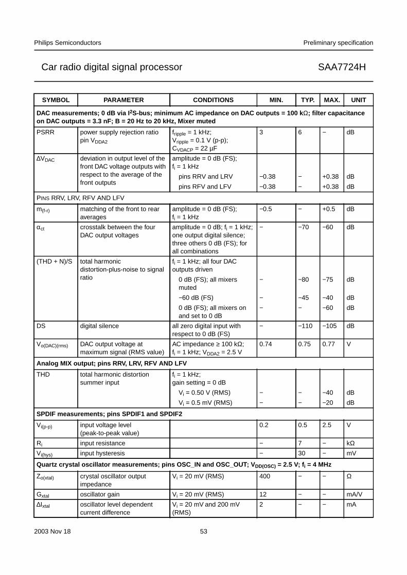
2003 Nov 18 53
Philips Semiconductors Preliminary specification
Car radio digital signal processor SAA7724H
DAC measurements; 0 dB via I 2S-bus; minimum AC impedance on DAC outputs = 100 k Ω; filter capacitanceon DAC outputs = 3.3 nF; B = 20 Hz to 20 kHz, Mixer muted
PSRR power supply rejection ratiopin VDDA2
fripple = 1 kHz;Vripple = 0.1 V (p-p);CVDACP = 22 µF
3 6 − dB
∆VDAC deviation in output level of thefront DAC voltage outputs withrespect to the average of thefront outputs
amplitude = 0 dB (FS);fi = 1 kHz
pins RRV and LRV −0.38 − +0.38 dB
pins RFV and LFV −0.38 − +0.38 dB
PINS RRV, LRV, RFV AND LFV
m(f-r) matching of the front to rearaverages
amplitude = 0 dB (FS);fi = 1 kHz
−0.5 − +0.5 dB
αct crosstalk between the fourDAC output voltages
amplitude = 0 dB; fi = 1 kHz;one output digital silence;three others 0 dB (FS); forall combinations
− −70 −60 dB
(THD + N)/S total harmonicdistortion-plus-noise to signalratio
fi = 1 kHz; all four DACoutputs driven
0 dB (FS); all mixersmuted
− −80 −75 dB
−60 dB (FS) − −45 −40 dB
0 dB (FS); all mixers onand set to 0 dB
− − −60 dB
DS digital silence all zero digital input withrespect to 0 dB (FS)
− −110 −105 dB
Vo(DAC)(rms) DAC output voltage atmaximum signal (RMS value)
AC impedance ≥ 100 kΩ;fi = 1 kHz; VDDA2 = 2.5 V
0.74 0.75 0.77 V
Analog MIX output; pins RRV, LRV, RFV AND LFV
THD total harmonic distortionsummer input
fi = 1 kHz;gain setting = 0 dB
Vi = 0.50 V (RMS) − − −40 dB
Vi = 0.5 mV (RMS) − − −20 dB
SPDIF measurements; pins SPDIF1 and SPDIF2
Vi(p-p) input voltage level(peak-to-peak value)
0.2 0.5 2.5 V
Ri input resistance − 7 − kΩVi(hys) input hysteresis − 30 − mV
Quartz crystal oscillator measurements; pins OSC_IN and OSC_OUT; V DD(OSC) = 2.5 V; f i = 4 MHz
Zo(xtal) crystal oscillator outputimpedance
Vi = 20 mV (RMS) 400 − − Ω
Gxtal oscillator gain Vi = 20 mV (RMS) 12 − − mA/V
∆Ixtal oscillator level dependentcurrent difference
Vi = 20 mV and 200 mV(RMS)
2 − − mA
SYMBOL PARAMETER CONDITIONS MIN. TYP. MAX. UNIT

2003 Nov 18 54
Philips Semiconductors Preliminary specification
Car radio digital signal processor SAA7724H
Digital output rise and fall times; T amb = 25 °C; CL = 30 pF
to(r) output rise time LOW-to-HIGHtransition
10 ns slew rate outputs − 10 − ns
4 mA outputs − 5 − ns
to(f) output fall time HIGH-to-LOWtransition
10 ns slew rate outputs − 10 − ns
4 mA outputs − 5 − ns
to(f)(SDA) output fall time HIGH-to-LOWtransition pin SDA
Cb = 10 pF to 400 pF 20 + 0.1Cb 250 ns
I2S-bus inputs and outputs (see Fig.29)
Tcy(BCK) I2S-bus bit clock cycle time fs = 48 kHz; pinsEXT_IIS_BCK1 andEXT_IIS_BCK2
81.3 − − ns
ts;DAT data set-up time pins EXT_IIS_IO1 andEXT_IIS_IO2
10 − − ns
pins IIS_IN1, IIS_IN2,IIS_IN3, IFP_IIS_IN1,IFP_IIS_I2O6 andIFP_IIS_I3O4
22.9 − − ns
th;DAT data hold time pins EXT_IIS_IO1 andEXT_IIS_IO2
5 − − ns
pins IIS_IN1, IIS_IN2,IIS_IN3, IFP_IIS_IN1,IFP_IIS_I2O6 andIFP_IIS_I3O4
0 − − ns
td;DAT data delay time pins IIS_OUT1, IIS_OUT2,IIS_OUT3, EXT_IIS_WS1,EXT_IIS_BCK1,EXT_IIS_IO1,EXT_IIS_WS2,EXT_IIS_BCK2 andEXT_IIS_IO2
− − 27 ns
ts;WS word select set-up time pins EXT_IIS_WS1 andEXT_IIS_WS2
10 − − ns
th;WS word select hold time pins EXT_IIS_WS1 andEXT_IIS_WS2
2 − − ns
td;WS word select delay time pins IIS_WS1 andIFP_IIS_WS
− − 27 ns
RDS inputs and outputs; pins RDS_DATA and RDS_BCK ; see Figs 30, 31, 32 and 33
TTDAV data valid period DAVA and DAVB mode 24.5 26.0 27.0 RDS bitperiods
DAVC mode 49.0 52.0 54.0 RDS bitperiods
tDAVNL time data available signal isLOW
DAVA, DAVB and DAVCmode
11.25 12.0 12.5 RDS bitperiods
tsr clock set-up time 100 − − µs
SYMBOL PARAMETER CONDITIONS MIN. TYP. MAX. UNIT
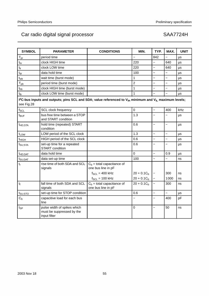
2003 Nov 18 55
Philips Semiconductors Preliminary specification
Car radio digital signal processor SAA7724H
Tpr period time − 842 − µs
thr clock HIGH time 220 − 640 µs
tlr clock LOW time 220 − 640 µs
tdr data hold time 100 − − µs
twb wait time (burst mode) 1 − − µs
Tpb period time (burst mode) 2 − − µs
thb clock HIGH time (burst mode) 1 − − µs
tlb clock LOW time (burst mode) 1 − − µs
I2C-bus inputs and outputs; pins SCL and SDA; value referenced to V IH minimum and V IL maximum levels;see Fig.28
fSCL SCL clock frequency 0 − 400 kHz
tBUF bus free time between a STOPand START condition
1.3 − − µs
tHD;STA hold time (repeated) STARTcondition
0.6 − − µs
tLOW LOW period of the SCL clock 1.3 − − µs
tHIGH HIGH period of the SCL clock 0.6 − − µs
tSU;STA set-up time for a repeatedSTART condition
0.6 − − µs
tHD;DAT data hold time 0 − 0.9 µs
tSU;DAT data set-up time 100 − − ns
tr rise time of both SDA and SCLsignals
Cb = total capacitance ofone bus line in pF
fSCL = 400 kHz 20 + 0.1Cb − 300 ns
fSCL = 100 kHz 20 + 0.1Cb − 1000 ns
tf fall time of both SDA and SCLsignals
Cb = total capacitance ofone bus line in pF
20 + 0.1Cb − 300 ns
tSU;STO set-up time for STOP condition 0.6 − − µs
Cb capacitive load for each busline
− − 400 pF
tSP pulse width of spikes whichmust be suppressed by theinput filter
0 − 50 ns
SYMBOL PARAMETER CONDITIONS MIN. TYP. MAX. UNIT

2003N
ov18
56
Philips S
emiconductors
Prelim
inary specification
Car radio digital signal processor
SA
A7724H
This text is here in white to force landscape pages to be rotated correctly when browsing through the pdf in the Acrobat reader.This text is here in_white to force landscape pages to be rotated correctly when browsing through the pdf in the Acrobat reader.This text is here inThis text is here inwhite to force landscape pages to be rotated correctly when browsing through the pdf in the Acrobat reader. white to force landscape pages to be ...
10.1T
iming diagram
s
hand
book
, ful
l pag
ewid
th
MBC611P S Sr P
tSU;STO
t SPt HD;STA
t SU;STAt SU;DAT
t f
t HIGH
t r
t HD;DAT
t LOW
t HD;STA
t BUF
SDA
SCL
Fig.28 Definition of timing on the I2C-bus.
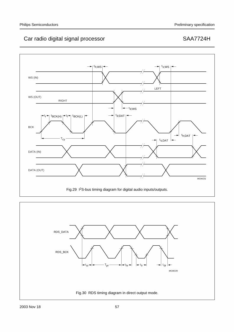
2003 Nov 18 57
Philips Semiconductors Preliminary specification
Car radio digital signal processor SAA7724H
handbook, full pagewidth ts;WS
td;WS
td;DAT
ts;DAT
th;DAT
tr tBCK(H) tBCK(L)tf
th;WS
LEFT
RIGHT
Tcy
WS (IN)
WS (OUT)
DATA (IN)
DATA (OUT)
BCK
MGW231
Fig.29 I2S-bus timing diagram for digital audio inputs/outputs.
handbook, full pagewidth
MGW226
RDS_DATA
RDS_BCK
tsr thr tlr tdrTpr
Fig.30 RDS timing diagram in direct output mode.
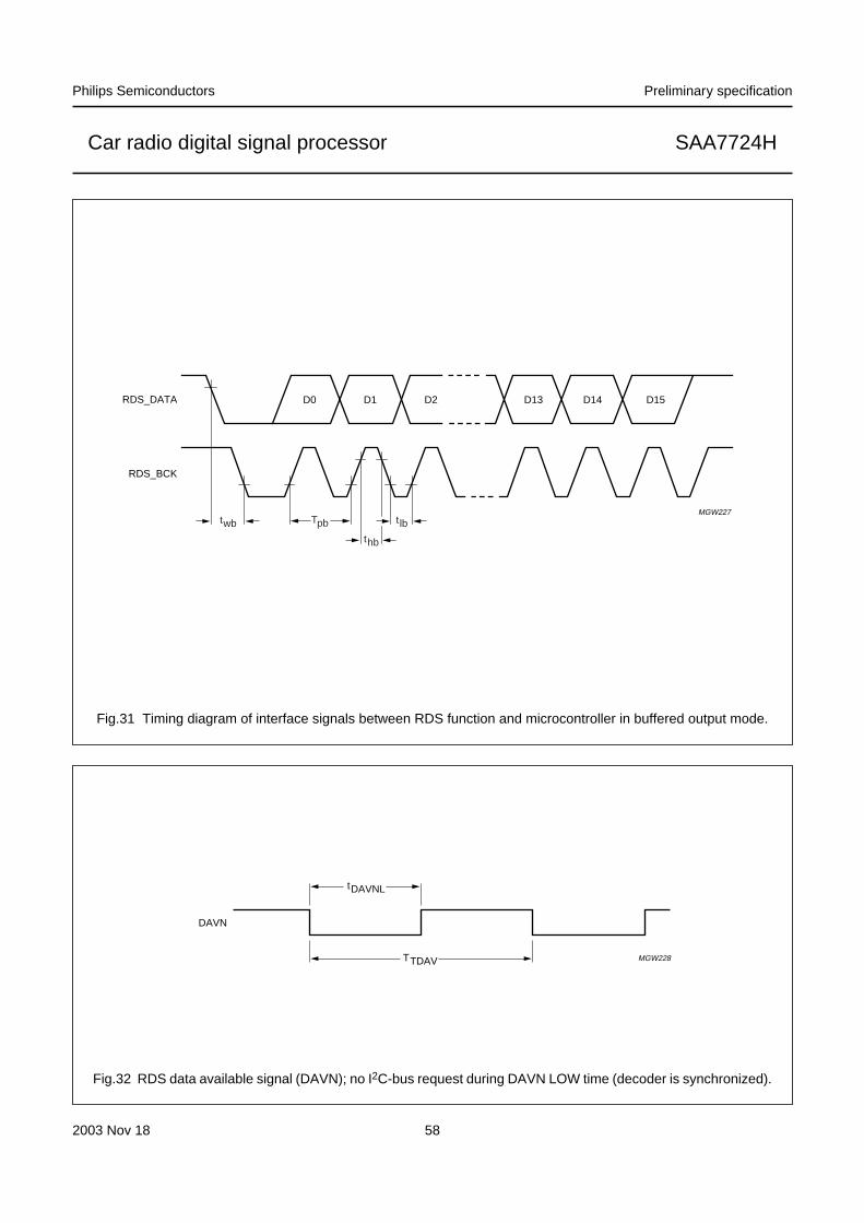
2003 Nov 18 58
Philips Semiconductors Preliminary specification
Car radio digital signal processor SAA7724H
handbook, full pagewidth
MGW227twb tlb
thb
Tpb
RDS_DATA D0 D1 D2 D13 D14 D15
RDS_BCK
Fig.31 Timing diagram of interface signals between RDS function and microcontroller in buffered output mode.
handbook, full pagewidth
MGW228
DAVN
tDAVNL
TTDAV
Fig.32 RDS data available signal (DAVN); no I2C-bus request during DAVN LOW time (decoder is synchronized).
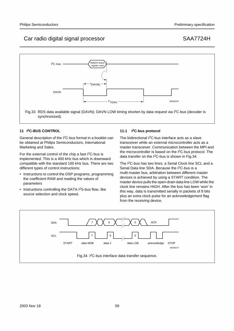
2003 Nov 18 59
Philips Semiconductors Preliminary specification
Car radio digital signal processor SAA7724H
handbook, full pagewidth
MGW229
I2C-bus
DAVN
tDAVNL
TTDAV
R(B)DS statusregister read
Fig.33 RDS data available signal (DAVN); DAVN LOW timing shorten by data request via I2C-bus (decoder issynchronized).
11 I2C-BUS CONTROL
General description of the I2C-bus format in a booklet canbe obtained at Philips Semiconductors, InternationalMarketing and Sales.
For the external control of the chip a fast I2C-bus isimplemented. This is a 400 kHz bus which is downwardcompatible with the standard 100 kHz bus. There are twodifferent types of control instructions:
• Instructions to control the DSP programs, programmingthe coefficient RAM and reading the values ofparameters
• Instructions controlling the DATA I2S-bus flow, likesource selection and clock speed.
11.1 I2C-bus protocol
The bidirectional I2C-bus interface acts as a slavetransceiver while an external microcontroller acts as amaster transceiver. Communication between the MPI andthe microcontroller is based on the I2C-bus protocol. Thedata transfer on the I2C-bus is shown in Fig.34.
The I2C-bus has two lines: a Serial Clock line SCL and aSerial Data line SDA. Because the I2C-bus is amulti-master bus, arbitration between different masterdevices is achieved by using a START condition. Themaster device pulls the open-drain data line LOW while theclock line remains HIGH. After the bus has been ‘won’ inthis way, data is transmitted serially in packets of 8 bitsplus an extra clock pulse for an acknowledgement flagfrom the receiving device.
handbook, full pagewidth
MGW217
START data MSB data 2 data LSB acknowledge STOP
067
0 ACK67SDA
SCL
Fig.34 I2C-bus interface data transfer sequence.
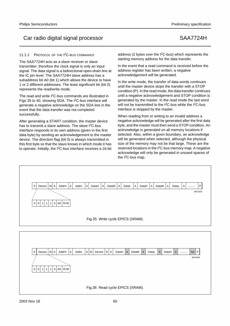
2003 Nov 18 60
Philips Semiconductors Preliminary specification
Car radio digital signal processor SAA7724H
11.1.1 PROTOCOL OF THE I2C-BUS COMMANDS
The SAA7724H acts as a slave receiver or slavetransmitter; therefore the clock signal is only an inputsignal. The data signal is a bidirectional open-drain line atthe IC pin level. The SAA7724H slave address has asubaddress bit A0 (bit 1) which allows the device to have1 or 2 different addresses. The least significant bit (bit 0)represents the read/write mode.
The read and write I2C-bus commands are illustrated inFigs 35 to 40, showing SDA. The I2C-bus interface willgenerate a negative acknowledge on the SDA line in theevent that the data transfer was not completedsuccessfully.
After generating a START condition, the master devicehas to transmit a slave address. The slave I2C-businterface responds to its own address (given in the firstdata byte) by sending an acknowledgement to the masterdevice. The direction flag (bit 0) is always transmitted inthis first byte so that the slave knows in which mode it hasto operate. Initially, the I2C-bus interface receives a 16-bit
address (2 bytes over the I2C-bus) which represents thestarting memory address for the data transfer.
In the event that a read command is received before theaddress register has been written, a negativeacknowledgement will be generated.
In the write mode, the transfer of data words continuesuntil the master device stops the transfer with a STOPcondition (P). In the read mode, the data transfer continuesuntil a negative acknowledgement and STOP condition isgenerated by the master. In the read mode the last wordwill not be transmitted to the I2C-bus while the I2C-businterface is stopped by the master.
When reading from or writing to an invalid address anegative acknowledge will be generated after the first databyte, and the master must then send a STOP condition. Anacknowledge is generated on all memory locations ifselected. Also, within a given boundary, an acknowledgewill be generated when selected, although the physicalsize of the memory may not be that large. These are thereserved locations in the I2C-bus memory map. A negativeacknowledge will only be generated in unused spaces ofthe I2C-bus map.
handbook, full pagewidth
MHC653
S Device W A AddrH A A AAddrL DataH DataM A DataL A ADataH DataM A A ...... PDataL
0 0 1 1 1 0 A0 R/W
Fig.35 Write cycle EPICS (XRAM).
handbook, full pagewidth
MHC654
S Device W A AddrH A A R AAddrL Device DataH A DataM A ADataL DataH A NA...... P
0 0 1 1 1 0 A0 R/W
Sr
Fig.36 Read cycle EPICS (XRAM).
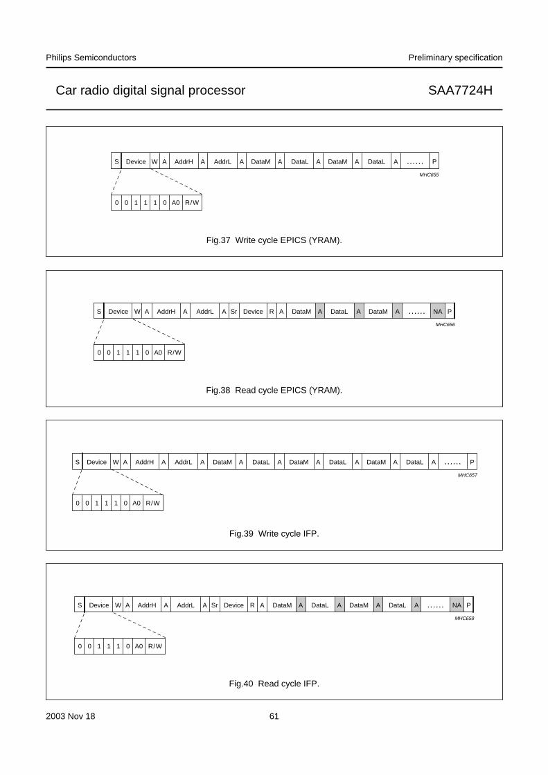
2003 Nov 18 61
Philips Semiconductors Preliminary specification
Car radio digital signal processor SAA7724H
handbook, full pagewidth
MHC655
S Device W A AddrH A A AAddrL DataM DataL A DataM A ADataL ...... P
0 0 1 1 1 0 A0 R/W
Fig.37 Write cycle EPICS (YRAM).
handbook, full pagewidth
MHC656
S Device W A AddrH A A R AAddrL Device DataM A DataL A ADataM NA...... P
0 0 1 1 1 0 A0 R/W
Sr
Fig.38 Read cycle EPICS (YRAM).
handbook, full pagewidth
MHC657
S Device W A AddrH A A AAddrL DataM DataL A DataM A ADataL DataM DataLA A ...... P
0 0 1 1 1 0 A0 R/W
Fig.39 Write cycle IFP.
handbook, full pagewidth
MHC658
S Device W A AddrH A A R AAddrL Device DataM A DataL A ADataM DataL A NA...... P
0 0 1 1 1 0 A0 R/W
Sr
Fig.40 Read cycle IFP.
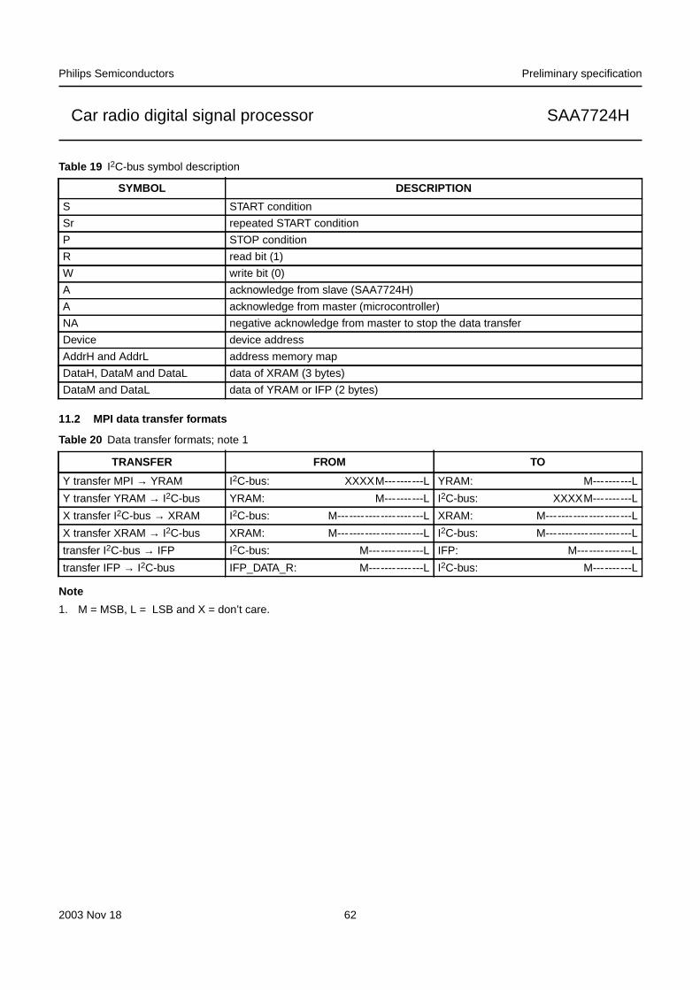
2003 Nov 18 62
Philips Semiconductors Preliminary specification
Car radio digital signal processor SAA7724H
Table 19 I2C-bus symbol description
11.2 MPI data transfer formats
Table 20 Data transfer formats; note 1
Note
1. M = MSB, L = LSB and X = don’t care.
SYMBOL DESCRIPTION
S START condition
Sr repeated START condition
P STOP condition
R read bit (1)
W write bit (0)
A acknowledge from slave (SAA7724H)
A acknowledge from master (microcontroller)
NA negative acknowledge from master to stop the data transfer
Device device address
AddrH and AddrL address memory map
DataH, DataM and DataL data of XRAM (3 bytes)
DataM and DataL data of YRAM or IFP (2 bytes)
TRANSFER FROM TO
Y transfer MPI → YRAM I2C-bus: XXXXM----------L YRAM: M----------L
Y transfer YRAM → I2C-bus YRAM: M----------L I2C-bus: XXXXM----------L
X transfer I2C-bus → XRAM I2C-bus: M----------------------L XRAM: M----------------------L
X transfer XRAM → I2C-bus XRAM: M----------------------L I2C-bus: M----------------------L
transfer I2C-bus → IFP I2C-bus: M--------------L IFP: M--------------L
transfer IFP → I2C-bus IFP_DATA_R: M--------------L I2C-bus: M----------L
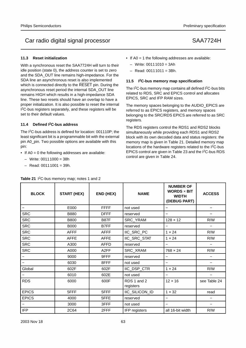
2003 Nov 18 63
Philips Semiconductors Preliminary specification
Car radio digital signal processor SAA7724H
11.3 Reset initialization
With a synchronous reset the SAA7724H will turn to theiridle position (state 0), the address counter is set to zeroand the SDA_OUT line remains high-impedance. For theSDA line an asynchronous reset is also implementedwhich is connected directly to the RESET pin. During theasynchronous reset period the internal SDA_OUT lineremains HIGH which results in a high-impedance SDAline. These two resets should have an overlap to have aproper initialization. It is also possible to reset the internalI2C-bus registers separately, and these registers will beset to their default values.
11.4 Defined I 2C-bus address
The I2C-bus address is defined for location: 001110P; theleast significant bit is a programmable bit with the externalpin A0_pin. Two possible options are available with thispin:
• If A0 = 0 the following addresses are available:
– Write: 00111000 = 38h
– Read: 00111001 = 39h.
• If A0 = 1 the following addresses are available:
– Write: 00111010 = 3Ah
– Read: 00111011 = 3Bh.
11.5 I2C-bus memory map specification
The I2C-bus memory map contains all defined I2C-bus bitsrelated to RDS, SRC and EPICS control and allocatesEPICS, SRC and IFP RAM sizes.
The memory spaces belonging to the AUDIO_EPICS arereferred to as EPICS registers, and memory spacesbelonging to the SRC/RDS EPICS are referred to as SRCregisters.
The RDS registers control the RDS1 and RDS2 blockssimultaneously while providing each RDS1 and RDS2block with its own decoded data and status registers: thememory map is given in Table 21. Detailed memory maplocations of the hardware registers related to the I2C-busEPICS control are given in Table 23 and the I2C-bus RDScontrol are given in Table 24.
Table 21 I2C-bus memory map; notes 1 and 2
BLOCK START (HEX) END (HEX) NAME
NUMBER OFWORDS × BIT
WIDTH(DEBUG PART)
ACCESS
− E000 FFFF not used − −SRC B880 DFFF reserved − −SRC B800 B87F SRC_YRAM 128 × 12 R/W
SRC B000 B7FF reserved − −SRC AFFF AFFF IIC_SRC_PC 1 × 24 R/W
SRC AFFE AFFE IIC_SRC_STAT 1 × 24 R/W
SRC A300 AFFD reserved − −SRC A000 A2FF SRC_XRAM 768 × 24 R/W
− 9000 9FFF reserved − −− 6030 8FFF not used − −Global 602F 602F IIC_DSP_CTR 1 × 24 R/W
− 6010 602E not used − −RDS 6000 600F RDS 1 and 2
registers12 × 16 see Table 24
EPICS 5FFF 5FFF IIC_SILICON_ID 1 × 32 read
EPICS 4000 5FFE reserved − −− 3000 3FFF not used − −IFP 2C64 2FFF IFP registers all 16-bit width R/W

2003 Nov 18 64
Philips Semiconductors Preliminary specification
Car radio digital signal processor SAA7724H
Notes
1. At all ‘reserved’ spaces an acknowledge (ACK) will be generated.
2. At all ‘not used’ spaces a negative acknowledge (NACK) will be generated.
Table 22 I2C-bus memory map SRC_EPICS hardware register overview
Table 23 I2C-bus memory map AUDIO_EPICS hardware register overview
− 1400 2C63 reserved − −IFP 2C00 2C63 FP_RAM 100 × 16 R/W
IFP 2700 2BFF reserved − −IFP 2600 26FF VY3_RAM 256 × 16 R/W
IFP 2500 25FF VX3_RAM 256 × 16 R/W
IFP 2400 24FF VY2_RAM 256 × 16 R/W
IFP 2300 23FF VX2_RAM 256 × 16 R/W
IFP 2200 22FF VY1_RAM 256 × 16 R/W
IFP 2100 21FF VX1_RAM 256 × 16 R/W
IFP 2081 20FF reserved − −IFP 2080 2080 IIC_SWB_ERR_STAT 1 × 16 R/W
IFP 2000 207F SWB_RAM 128 × 16 R/W
EPICS 1400 1FFF reserved − −EPICS 1000 13FF EPICS_YRAM 1024 × 12 R/W
EPICS 0FFF 0FFF IIC_EPICS_PC 1 × 24 R/W
EPICS 0FFE 0FFE IIC_EPICS_STAT 1 × 24 R/W
EPICS 0FF0 0FFD EPICS registers 14 × 24 R/W
EPICS 0E00 0FEF reserved − −EPICS 0000 0DFF EPICS_XRAM 3584 × 24 R/W
LOCATION (HEX) REGISTER NAME # USED BITS READ/WRITE
AFFF IIC_SRC_PC 24 R/W
AFFE IIC_SRC_STAT 24 R/W
LOCATION (HEX) REGISTER NAME # USED BITS READ/WRITE
0FFF IIC_EPICS_PC 24 R/W
0FFE IIC_EPICS_STAT 24 R/W
0FFD IIC_DSPIO_CONF 9 R/W
0FFC IIC_SEL 20 R/W
0FFB IIC_IFAD_SEL 10 R/W
0FFA IIC_HOST 12 R/W
BLOCK START (HEX) END (HEX) NAME
NUMBER OFWORDS × BIT
WIDTH(DEBUG PART)
ACCESS

2003 Nov 18 65
Philips Semiconductors Preliminary specification
Car radio digital signal processor SAA7724H
Table 24 I2C-bus memory map RDS hardware register overview
Table 25 I2C_EPICS_STAT status register (0FFEh)
0FF9 IIC_SPDIF_STAT 13 read
0FF8 IIC_SUM 13 R/W
0FF7 IIC_EPICS_START_ADDR 16 R/W
LOCATION (HEX) REGISTER NAME # USED BITS READ/WRITE
600F and 600E not used − −600D IIC_RDS2_CTR 11 write
600C IIC_RDS2_SET 15 write
600B IIC_RDS2_CNT 16 read
600A IIC_RDS2_PDAT 16 read
6009 IIC_RDS2_LDAT 16 read
6008 IIC_RDS2_STAT 8 read
6007 and 6006 not used − −6005 IIC_RDS1_CTR 11 write
6004 IIC_RDS1_SET 15 write
6003 IIC_RDS1_CNT 16 read
6002 IIC_RDS1_PDAT 16 read
6001 IIC_RDS1_LDAT 16 read
6000 IIC_RDS1_STAT 8 read
BIT SYMBOL DEFAULT DESCRIPTION
23 to 13 − 0h internal flags
12 and 11 F12 and F11 − not used
10 F10 0 SPDIF2 lock status
0: not locked
1: locked
9 F9 0 SPDIF1 lock status
0: not locked
1: locked
8 F8 0 DSPIO8 status
0: input
1: output
7 F7 0 DSPIO7 status
0: input
1: output
6 F6 0 DSPIO6 status
0: input
1: output
LOCATION (HEX) REGISTER NAME # USED BITS READ/WRITE
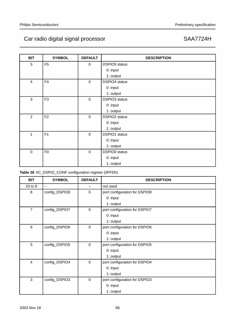
2003 Nov 18 66
Philips Semiconductors Preliminary specification
Car radio digital signal processor SAA7724H
Table 26 IIC_DSPIO_CONF configuration register (0FFDh)
5 F5 0 DSPIO5 status
0: input
1: output
4 F4 0 DSPIO4 status
0: input
1: output
3 F3 0 DSPIO3 status
0: input
1: output
2 F2 0 DSPIO2 status
0: input
1: output
1 F1 0 DSPIO1 status
0: input
1: output
0 F0 0 DSPIO0 status
0: input
1: output
BIT SYMBOL DEFAULT DESCRIPTION
23 to 9 − − not used
8 config_DSPIO8 0 port configuration for DSPIO8
0: input
1: output
7 config_DSPIO7 0 port configuration for DSPIO7
0: input
1: output
6 config_DSPIO6 0 port configuration for DSPIO6
0: input
1: output
5 config_DSPIO5 0 port configuration for DSPIO5
0: input
1: output
4 config_DSPIO4 0 port configuration for DSPIO4
0: input
1: output
3 config_DSPIO3 0 port configuration for DSPIO3
0: input
1: output
BIT SYMBOL DEFAULT DESCRIPTION
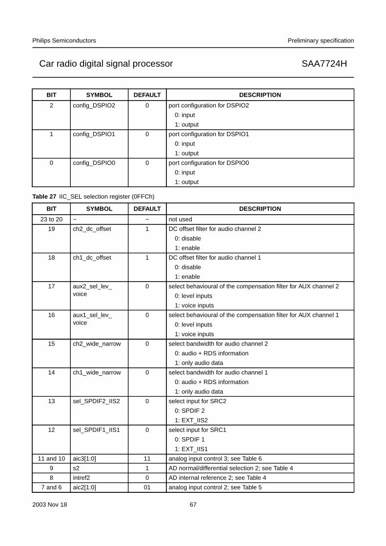
2003 Nov 18 67
Philips Semiconductors Preliminary specification
Car radio digital signal processor SAA7724H
Table 27 IIC_SEL selection register (0FFCh)
2 config_DSPIO2 0 port configuration for DSPIO2
0: input
1: output
1 config_DSPIO1 0 port configuration for DSPIO1
0: input
1: output
0 config_DSPIO0 0 port configuration for DSPIO0
0: input
1: output
BIT SYMBOL DEFAULT DESCRIPTION
23 to 20 − − not used
19 ch2_dc_offset 1 DC offset filter for audio channel 2
0: disable
1: enable
18 ch1_dc_offset 1 DC offset filter for audio channel 1
0: disable
1: enable
17 aux2_sel_lev_voice
0 select behavioural of the compensation filter for AUX channel 2
0: level inputs
1: voice inputs
16 aux1_sel_lev_voice
0 select behavioural of the compensation filter for AUX channel 1
0: level inputs
1: voice inputs
15 ch2_wide_narrow 0 select bandwidth for audio channel 2
0: audio + RDS information
1: only audio data
14 ch1_wide_narrow 0 select bandwidth for audio channel 1
0: audio + RDS information
1: only audio data
13 sel_SPDIF2_IIS2 0 select input for SRC2
0: SPDIF 2
1: EXT_IIS2
12 sel_SPDIF1_IIS1 0 select input for SRC1
0: SPDIF 1
1: EXT_IIS1
11 and 10 aic3[1:0] 11 analog input control 3; see Table 6
9 s2 1 AD normal/differential selection 2; see Table 4
8 intref2 0 AD internal reference 2; see Table 4
7 and 6 aic2[1:0] 01 analog input control 2; see Table 5
BIT SYMBOL DEFAULT DESCRIPTION

2003 Nov 18 68
Philips Semiconductors Preliminary specification
Car radio digital signal processor SAA7724H
Table 28 IIC_IFAD_SEL selection register (0FFBh)
Table 29 IIC_HOST register (0FFAh)
5 refc2 1 AD reference control 2; see Table 4
4 s1 0 AD normal/differential selection 1; see Table 4
3 intref1 0 AD internal reference 1; see Table 4
2 and 1 aic1[1:0] 00 analog input control 1; see Table 5
0 refc1 0 AD reference control 1; see Table 4
BIT SYMBOL DEFAULT DESCRIPTION
23 to 10 − − not used
9 ifad2_power 1 controls activity of IFAD2
0: power low
1: power on
8 ifad1_power 1 controls activity of IFAD1
0: power low
1: power on
7 to 4 dith_gain_2[3:0] 0000 control gain of IF-AD dither source 2
3 to 0 dith_gain_1[3:0] 0000 control gain of IF-AD dither source 1
BIT SYMBOL DEFAULT DESCRIPTION
23 to 20 − − not used
19 src2_ext_sel_out 0 selects the external output port for SRC2
0: EXT_IIS1
1: EXT_IIS2
18 src1_ext_sel_out 1 selects the external output port for SRC1
0: EXT_IIS1
1: EXT_IIS2
17 src2_int_ext_out 0 selects the output destination for SRC2
0: internal (audio epics)
1: external (Ext_iis)
16 src1_int_ext_out 0 selects the output destination for SRC1
0: internal (audio epics)
1: external (Ext_iis)
15 src2_int_ext_in 1 selects the input source for SRC2
0: internal (audio epics)
1: external (Ext_iis/Spdif)
14 src1_int_ext_in 1 selects the input source for SRC1
0: internal (audio epics)
1: external (Ext_iis/Spdif)
BIT SYMBOL DEFAULT DESCRIPTION
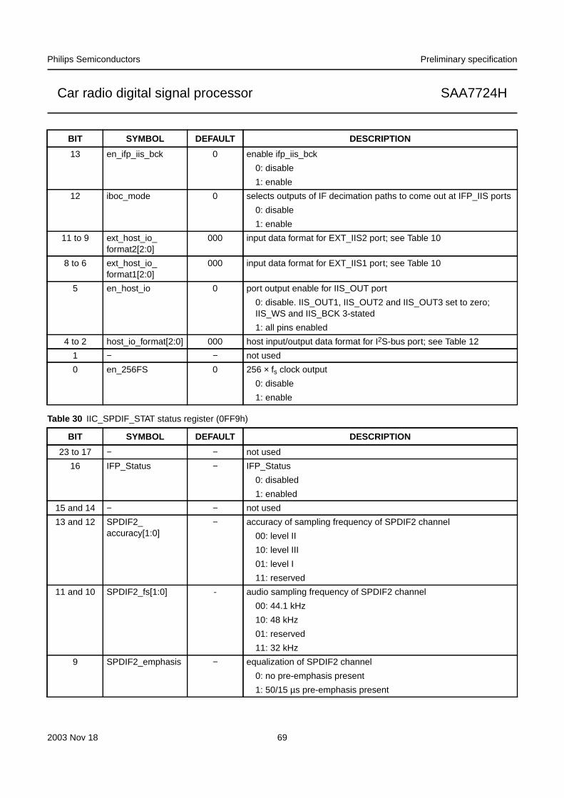
2003 Nov 18 69
Philips Semiconductors Preliminary specification
Car radio digital signal processor SAA7724H
Table 30 IIC_SPDIF_STAT status register (0FF9h)
13 en_ifp_iis_bck 0 enable ifp_iis_bck
0: disable
1: enable
12 iboc_mode 0 selects outputs of IF decimation paths to come out at IFP_IIS ports
0: disable
1: enable
11 to 9 ext_host_io_format2[2:0]
000 input data format for EXT_IIS2 port; see Table 10
8 to 6 ext_host_io_format1[2:0]
000 input data format for EXT_IIS1 port; see Table 10
5 en_host_io 0 port output enable for IIS_OUT port
0: disable. IIS_OUT1, IIS_OUT2 and IIS_OUT3 set to zero;IIS_WS and IIS_BCK 3-stated
1: all pins enabled
4 to 2 host_io_format[2:0] 000 host input/output data format for I2S-bus port; see Table 12
1 − − not used
0 en_256FS 0 256 × fs clock output
0: disable
1: enable
BIT SYMBOL DEFAULT DESCRIPTION
23 to 17 − − not used
16 IFP_Status − IFP_Status
0: disabled
1: enabled
15 and 14 − − not used
13 and 12 SPDIF2_accuracy[1:0]
− accuracy of sampling frequency of SPDIF2 channel
00: level II
10: level III
01: level I
11: reserved
11 and 10 SPDIF2_fs[1:0] - audio sampling frequency of SPDIF2 channel
00: 44.1 kHz
10: 48 kHz
01: reserved
11: 32 kHz
9 SPDIF2_emphasis − equalization of SPDIF2 channel
0: no pre-emphasis present
1: 50/15 µs pre-emphasis present
BIT SYMBOL DEFAULT DESCRIPTION
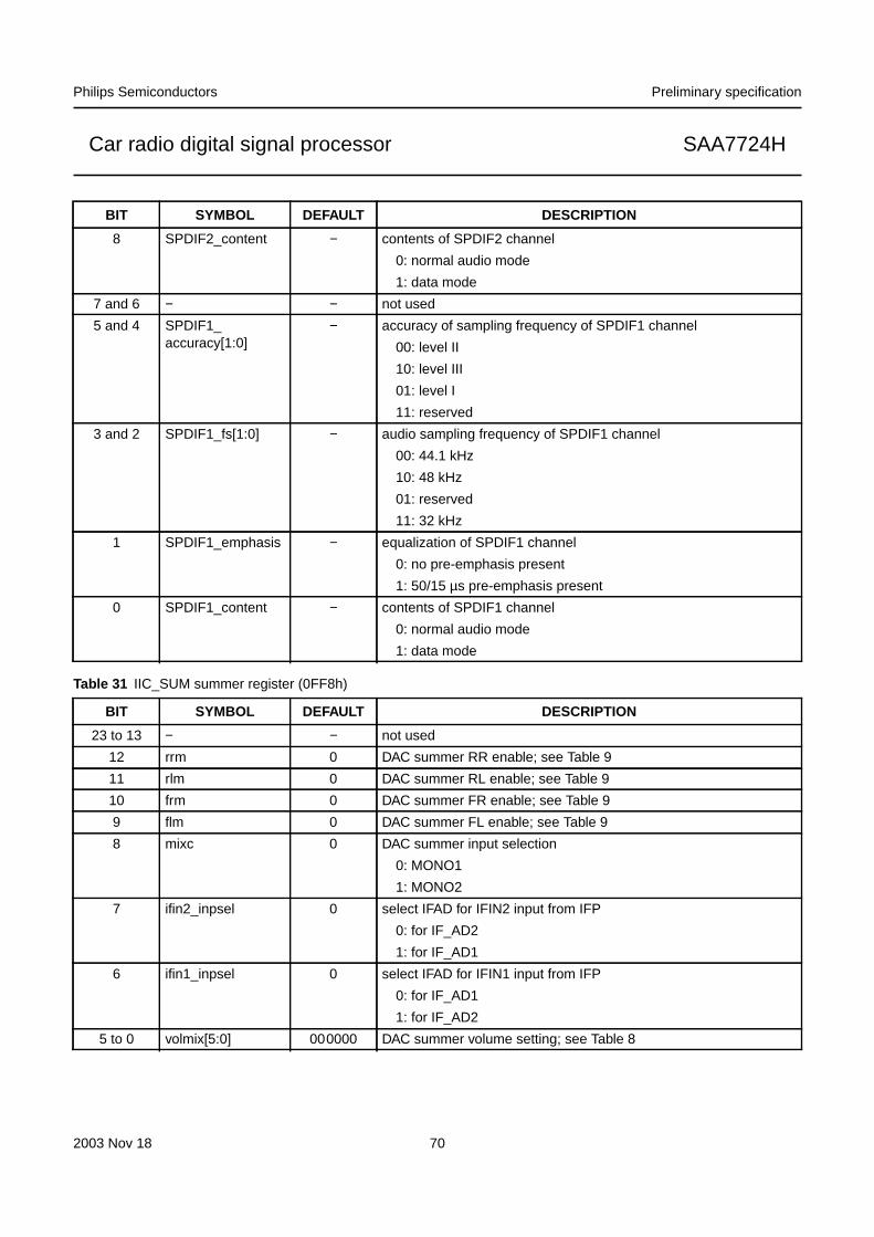
2003 Nov 18 70
Philips Semiconductors Preliminary specification
Car radio digital signal processor SAA7724H
Table 31 IIC_SUM summer register (0FF8h)
8 SPDIF2_content − contents of SPDIF2 channel
0: normal audio mode
1: data mode
7 and 6 − − not used
5 and 4 SPDIF1_accuracy[1:0]
− accuracy of sampling frequency of SPDIF1 channel
00: level II
10: level III
01: level I
11: reserved
3 and 2 SPDIF1_fs[1:0] − audio sampling frequency of SPDIF1 channel
00: 44.1 kHz
10: 48 kHz
01: reserved
11: 32 kHz
1 SPDIF1_emphasis − equalization of SPDIF1 channel
0: no pre-emphasis present
1: 50/15 µs pre-emphasis present
0 SPDIF1_content − contents of SPDIF1 channel
0: normal audio mode
1: data mode
BIT SYMBOL DEFAULT DESCRIPTION
23 to 13 − − not used
12 rrm 0 DAC summer RR enable; see Table 9
11 rlm 0 DAC summer RL enable; see Table 9
10 frm 0 DAC summer FR enable; see Table 9
9 flm 0 DAC summer FL enable; see Table 9
8 mixc 0 DAC summer input selection
0: MONO1
1: MONO2
7 ifin2_inpsel 0 select IFAD for IFIN2 input from IFP
0: for IF_AD2
1: for IF_AD1
6 ifin1_inpsel 0 select IFAD for IFIN1 input from IFP
0: for IF_AD1
1: for IF_AD2
5 to 0 volmix[5:0] 000000 DAC summer volume setting; see Table 8
BIT SYMBOL DEFAULT DESCRIPTION
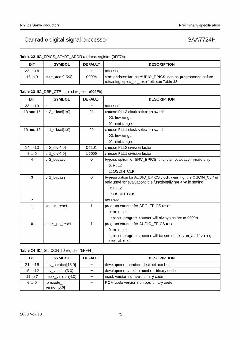
2003 Nov 18 71
Philips Semiconductors Preliminary specification
Car radio digital signal processor SAA7724H
Table 32 IIC_EPICS_START_ADDR address register (0FF7h)
Table 33 IIC_DSP_CTR control register (602Fh)
Table 34 IIC_SILICON_ID register (5FFFh);
BIT SYMBOL DEFAULT DESCRIPTION
23 to 16 − − not used
15 to 0 start_addr[15:0] 0000h start address for the AUDIO_EPICS; can be programmed beforereleasing ‘epics_pc_reset’ bit; see Table 33
BIT SYMBOL DEFAULT DESCRIPTION
23 to 19 − − not used
18 and 17 pll2_clksel[1:0] 01 choose PLL2 clock selection switch
00: low range
01: mid range
16 and 15 pll1_clksel[1:0] 00 choose PLL1 clock selection switch
00: low range
01: mid range
14 to 10 pll2_div[4:0] 01101 choose PLL2 division factor
9 to 5 pll1_div[4:0] 10000 choose PLL1 division factor
4 pll2_bypass 0 bypass option for SRC_EPICS; this is an evaluation mode only
0: PLL2
1: OSCIN_CLK
3 pll1_bypass 0 bypass option for AUDIO_EPICS clock; warning: the OSCIN_CLK isonly used for evaluation; it is functionally not a valid setting
0: PLL2
1: OSCIN_CLK
2 − − not used
1 src_pc_reset 1 program counter for SRC_EPICS reset
0: no reset
1: reset; program counter will always be set to 0000h
0 epics_pc_reset 1 program counter for AUDIO_EPICS reset
0: no reset
1: reset; program counter will be set to the ‘start_addr’ value;see Table 32
BIT SYMBOL DEFAULT DESCRIPTION
31 to 16 dev_number[15:0] − development number; decimal number
15 to 12 dev_version[3:0] − development version number; binary code
11 to 7 mask_version[4:0] − mask version number; binary code
6 to 0 romcode_version[6:0]
− ROM code version number; binary code
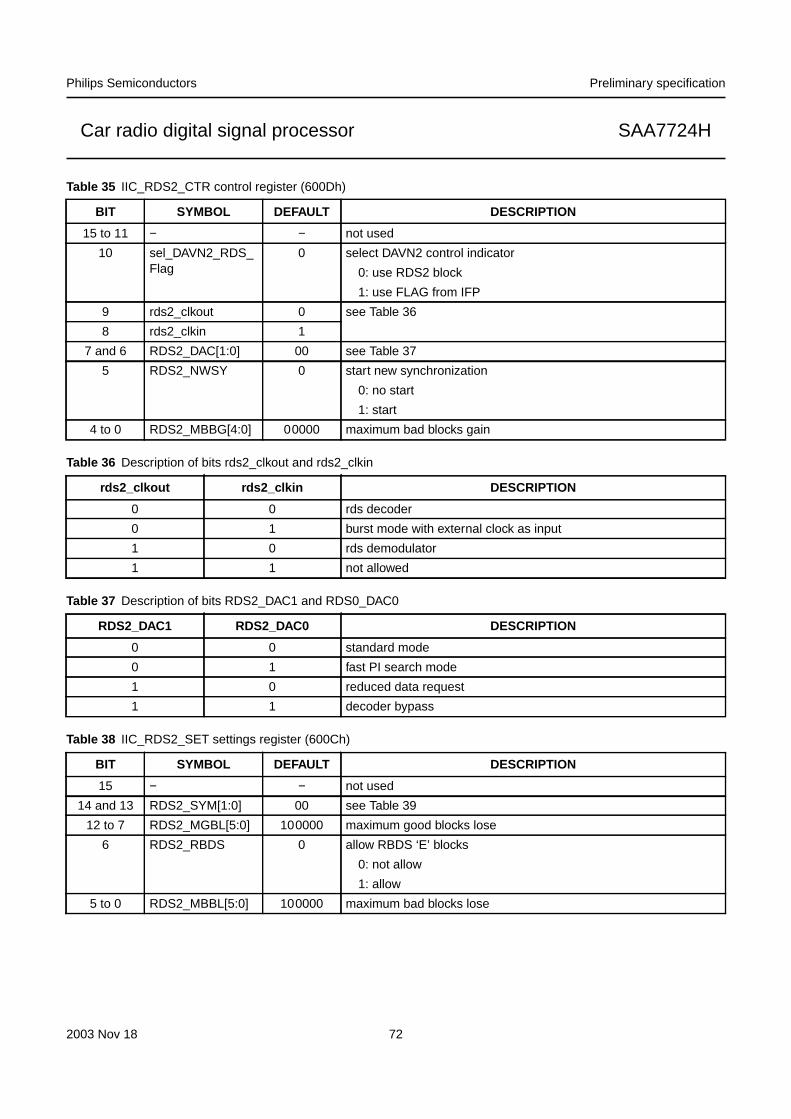
2003 Nov 18 72
Philips Semiconductors Preliminary specification
Car radio digital signal processor SAA7724H
Table 35 IIC_RDS2_CTR control register (600Dh)
Table 36 Description of bits rds2_clkout and rds2_clkin
Table 37 Description of bits RDS2_DAC1 and RDS0_DAC0
Table 38 IIC_RDS2_SET settings register (600Ch)
BIT SYMBOL DEFAULT DESCRIPTION
15 to 11 − − not used
10 sel_DAVN2_RDS_Flag
0 select DAVN2 control indicator
0: use RDS2 block
1: use FLAG from IFP
9 rds2_clkout 0 see Table 36
8 rds2_clkin 1
7 and 6 RDS2_DAC[1:0] 00 see Table 37
5 RDS2_NWSY 0 start new synchronization
0: no start
1: start
4 to 0 RDS2_MBBG[4:0] 00000 maximum bad blocks gain
rds2_clkout rds2_clkin DESCRIPTION
0 0 rds decoder
0 1 burst mode with external clock as input
1 0 rds demodulator
1 1 not allowed
RDS2_DAC1 RDS2_DAC0 DESCRIPTION
0 0 standard mode
0 1 fast PI search mode
1 0 reduced data request
1 1 decoder bypass
BIT SYMBOL DEFAULT DESCRIPTION
15 − − not used
14 and 13 RDS2_SYM[1:0] 00 see Table 39
12 to 7 RDS2_MGBL[5:0] 100000 maximum good blocks lose
6 RDS2_RBDS 0 allow RBDS ‘E’ blocks
0: not allow
1: allow
5 to 0 RDS2_MBBL[5:0] 100000 maximum bad blocks lose

2003 Nov 18 73
Philips Semiconductors Preliminary specification
Car radio digital signal processor SAA7724H
Table 39 Description of bits RDS2_SYM1 and RDS2_SYM0
Table 40 IIC_RDS2_CNT counter register (600Bh)
Table 41 Description of bits RDS2_EPB1 and RDS2_EPB0
Table 42 IIC_RDS2_PDAT register (600Ah)
Table 43 IIC_RDS2_LDAT register (6009h)
Table 44 IIC_RDS2_STAT status register (6008h)
RDS2_SYM1 RDS2_SYMO DESCRIPTION
0 0 no error correction
0 1 maximum 2 bits burst error
1 0 maximum 5 bits burst error
1 1 no error correction
BIT SYMBOL DEFAULT DESCRIPTION
15 to 10 RDS2_BBC[5:0] 000000 bad blocks counter
9 to 5 RDS2_GBC[4:0] 00000 good blocks counter (only 5 MSBs are available)
4 to 2 RDS2_PBIN[2:0] 111 previous block identifier
1 and 0 RDS2_EPB[1:0] 00 error status previously received block; see Table 41
RDS2_EPB1 RDS2_EPB0 DESCRIPTION
0 0 no errors detected
0 1 maximum 2 bits
1 0 maximum 5 bits
1 1 uncorrectable
BIT SYMBOL DEFAULT DESCRIPTION
15 to 0 RDS2_PDAT[15:0] 0000h previously processed block data
BIT SYMBOL DEFAULT DESCRIPTION
15 to 0 RDS2_LDAT[15:0] 0000h last processed block data
BIT SYMBOL DEFAULT DESCRIPTION
15 to 8 − − not used
7 RDS2_SYNC 0 synchronization found
0: no synchronization
1: synchronization
6 RDS2_DOFL 0 data overflow flag
0: no overflow
1: overflow
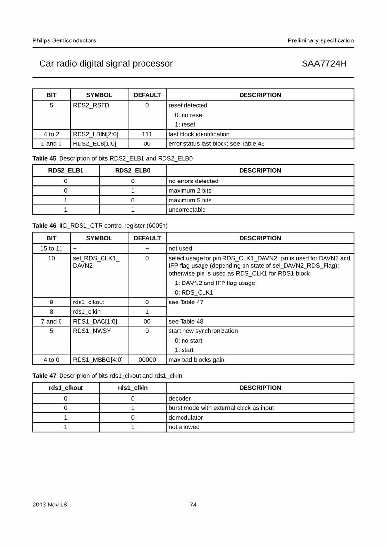
2003 Nov 18 74
Philips Semiconductors Preliminary specification
Car radio digital signal processor SAA7724H
Table 45 Description of bits RDS2_ELB1 and RDS2_ELB0
Table 46 IIC_RDS1_CTR control register (6005h)
Table 47 Description of bits rds1_clkout and rds1_clkin
5 RDS2_RSTD 0 reset detected
0: no reset
1: reset
4 to 2 RDS2_LBIN[2:0] 111 last block identification
1 and 0 RDS2_ELB[1:0] 00 error status last block; see Table 45
RDS2_ELB1 RDS2_ELB0 DESCRIPTION
0 0 no errors detected
0 1 maximum 2 bits
1 0 maximum 5 bits
1 1 uncorrectable
BIT SYMBOL DEFAULT DESCRIPTION
15 to 11 − − not used
10 sel_RDS_CLK1_DAVN2
0 select usage for pin RDS_CLK1_DAVN2; pin is used for DAVN2 andIFP flag usage (depending on state of sel_DAVN2_RDS_Flag);otherwise pin is used as RDS_CLK1 for RDS1 block
1: DAVN2 and IFP flag usage
0: RDS_CLK1
9 rds1_clkout 0 see Table 47
8 rds1_clkin 1
7 and 6 RDS1_DAC[1:0] 00 see Table 48
5 RDS1_NWSY 0 start new synchronization
0: no start
1: start
4 to 0 RDS1_MBBG[4:0] 00000 max bad blocks gain
rds1_clkout rds1_clkin DESCRIPTION
0 0 decoder
0 1 burst mode with external clock as input
1 0 demodulator
1 1 not allowed
BIT SYMBOL DEFAULT DESCRIPTION
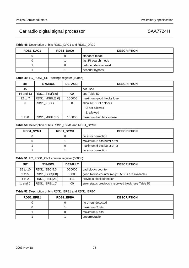
2003 Nov 18 75
Philips Semiconductors Preliminary specification
Car radio digital signal processor SAA7724H
Table 48 Description of bits RDS1_DAC1 and RDS1_DAC0
Table 49 IIC_RDS1_SET settings register (6004h)
Table 50 Description of bits RDS1_SYM1 and RDS1_SYM0
Table 51 IIC_RDS1_CNT counter register (6003h)
Table 52 Description of bits RDS1_EPB1 and RDS1_EPB0
RDS1_DAC1 RDS1_DAC0 DESCRIPTION
0 0 standard mode
0 1 fast PI search mode
1 0 reduced data request
1 1 decoder bypass
BIT SYMBOL DEFAULT DESCRIPTION
15 − − not used
14 and 13 RDS1_SYM[1:0] 00 see Table 50
12 to 7 RDS1_MGBL[5:0] 100000 maximum good blocks lose
6 RDS1_RBDS 0 allow RBDS ‘E’ blocks
0: not allowed
1: allowed
5 to 0 RDS1_MBBL[5:0] 100000 maximum bad blocks lose
RDS1_SYM1 RDS1_SYM0 DESCRIPTION
0 0 no error correction
0 1 maximum 2 bits burst error
1 0 maximum 5 bits burst error
1 1 no error correction
BIT SYMBOL DEFAULT DESCRIPTION
15 to 10 RDS1_BBC[5:0] 000000 bad blocks counter
9 to 5 RDS1_GBC[4:0] 00000 good blocks counter (only 5 MSBs are available)
4 to 2 RDS1_PBIN[2:0] 111 previous block identifier
1 and 0 RDS1_EPB[1:0] 00 error status previously received block; see Table 52
RDS1_EPB1 RDS1_EPB0 DESCRIPTION
0 0 no errors detected
0 1 maximum 2 bits
1 0 maximum 5 bits
1 1 uncorrectable

2003 Nov 18 76
Philips Semiconductors Preliminary specification
Car radio digital signal processor SAA7724H
Table 53 IIC_RDS1_PDAT register (6002h)
Table 54 IIC_RDS1_LDAT register (6001h)
Table 55 IIC_RDS1_STAT status register (6000h)
Table 56 Description of bits RDS1_ELB1 and RDS1_ELB0
BIT SYMBOL DEFAULT DESCRIPTION
15 to 0 RDS1_PDAT[15:0] 0000h previously processed block data
BIT SYMBOL DEFAULT DESCRIPTION
15 to 0 RDS1_LDAT[15:0] 0000h last processed block data
BIT SYMBOL DEFAULT DESCRIPTION
15 to 8 − - not used
7 RDS1_SYNC 0 synchronization found
0: no synchronization
1: synchronization
6 RDS1_DOFL 0 data overflow flag
0: no overflow
1: overflow
5 RDS1_RSTD 0 reset detected
0: no reset
1: reset
4 to 2 RDS1_LBIN[2:0] 111 last block identification
1 and 0 RDS1_ELB[1:0] 00 error status last block; see Table 56
RDS1_ELB1 RDS1_ELB0 DESCRIPTION
0 0 no errors detected
0 1 maximum 2 bits
1 0 maximum 5 bits
1 1 uncorrectable

2003 Nov 18 77
Philips Semiconductors Preliminary specification
Car radio digital signal processor SAA7724H
12 I2S-BUS CONTROL
12.1 Basic system requirements
The inter-IC sound (I2S-bus) was developed by Philips tofacilitate communications between the ever increasingnumber of digital audio processing ICs in a typical audiosystem. The bus only has to handle audio data, while theother signals such as sub-coding and control aretransferred separately. To minimize the number of pinsrequired and to keep wiring simple, a 3-line serial bus isused consisting of a line for two time-multiplexed datachannels, a word select line and a clock line.
Since the transmitter and receiver have the same clocksignal for data transmission, the transmitter as the master,has to generate the bit clock, word select signal and data.In complex systems however, there may be several
transmitters and receivers which makes it difficult to definethe master. In such systems there is usually a systemmaster controlling digital audio data-flow between thevarious ICs. Transmitters then have to generate dataunder the control of an external clock, and so act as aslave. Figure 41 illustrates some simple systemconfigurations and the basic interface timing. Note that thesystem master can be combined with a transmitter orreceiver, and it may be enabled or disabled under softwarecontrol or by pin programming.
As shown in Fig.41, the bus has three lines:
• Continuous serial clock (SCK)
• Word Select (WS)
• Serial Data (SD).
The device generating SCK and WS is the master.
handbook, full pagewidth
MGW230
WSRECEIVER
RECEIVER = MASTER
TRANSMITTER
SCK
SD
Word Select WSRECEIVER
TRANSMITTER = MASTER
TRANSMITTER
Clock SCK
Data SD
WSRECEIVER
MSB
SCK
WS
SD
word nleft channel
word n + 1right channel
word n − 1right channel
LSB MSB
CONTROLLER = MASTER
TRANSMITTER
CONTROLLER
SCK
SD
Fig.41 Simple system configurations and basic interface timing.
2003 Nov 18 78
Philips Semiconductors Preliminary specification
Car radio digital signal processor SAA7724H
12.2 Serial data
Serial data is transmitted in twos complement with theMSB first. The MSB is transmitted first because thetransmitter and receiver may have different word lengths.It is not necessary for the transmitter to know how manybits the receiver can handle, nor does the receiver need toknow how many bits are being transmitted.
When the system word length is greater than thetransmitter word length, the word is truncated (leastsignificant bits are set to 0) for data transmission. If thereceiver is sent more bits than it’s word length, the bitsafter the LSB are ignored. However, if the receiver is sentfewer bits than it’s word length the missing bits are set tozero internally. Therefore, the MSB has a fixed positionwhereas the position of the LSB depends on the wordlength. The transmitter always sends the MSB of the nextword one clock period after the WS changes.
Serial data sent by the transmitter may be synchronizedwith either the trailing (HIGH-to-LOW) or the leading(LOW-to-HIGH) edge of the clock signal. However, theserial data must be latched into the receiver on the leadingedge of the serial clock signal so there are somerestrictions when transmitting data that is synchronizedwith the leading edge.
12.3 Word select
The word select line indicates the channel beingtransmitted:
• WS = 0: channel 1 (left)
• WS = 1: channel 2 (right).
WS may change either on a trailing or leading edge of theserial clock, but it doesn’t need to be symmetrical. In theslave, this signal is latched on the leading edge of the clocksignal. The WS line changes one clock period before theMSB is transmitted. This allows the slave transmitter toderive synchronous timing of the serial data that will be setup for transmission. Furthermore, it enables the receiver tostore the previous word and clear the input for the nextword (see Fig.41).
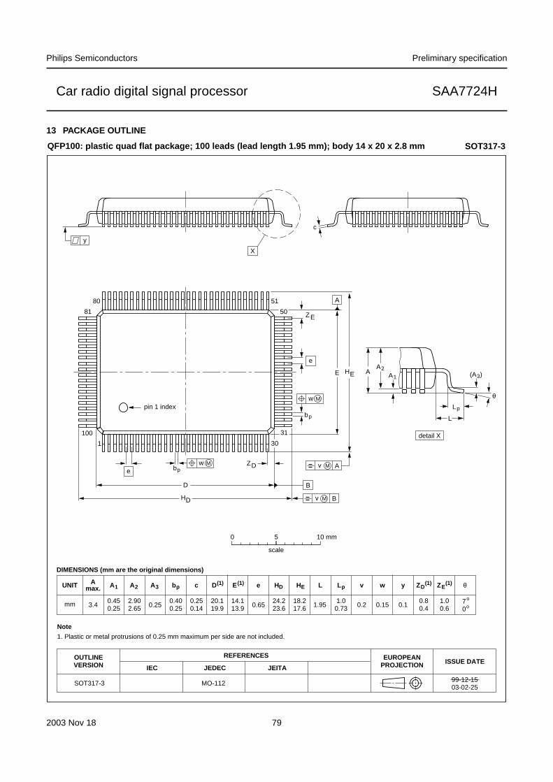
2003 Nov 18 79
Philips Semiconductors Preliminary specification
Car radio digital signal processor SAA7724H
13 PACKAGE OUTLINE
UNIT A1 A2 A3 bp c E(1) e HE L L p Zywv θ
REFERENCESOUTLINEVERSION
EUROPEANPROJECTION ISSUE DATE
IEC JEDEC JEITA
mm 0.450.25
2.902.65 0.25
0.400.25
0.250.14
14.113.9 0.65
18.217.6
1.00.6
70
o
o0.15 0.10.21.95
DIMENSIONS (mm are the original dimensions)
Note
1. Plastic or metal protrusions of 0.25 mm maximum per side are not included.
1.00.73
SOT317-3 MO-112
D(1) (1)(1)
20.119.9
HD
24.223.6
EZ
0.80.4
D
e
θ
E A1A
Lp
detail X
L
(A )3
B
30
c
bp
EHA2
D
ZD
A
ZE
e
v M A
1
100
81
80 51
50
31
pin 1 index
X
y
bp
DH v M B
w M
w M
0 5 10 mm
scale
QFP100: plastic quad flat package; 100 leads (lead length 1.95 mm); body 14 x 20 x 2.8 mm SOT317-3
Amax.
3.4
99-12-1503-02-25
2003 Nov 18 80
Philips Semiconductors Preliminary specification
Car radio digital signal processor SAA7724H
14 SOLDERING
14.1 Introduction to soldering surface mountpackages
This text gives a very brief insight to a complex technology.A more in-depth account of soldering ICs can be found inour “Data Handbook IC26; Integrated Circuit Packages”(document order number 9398 652 90011).
There is no soldering method that is ideal for all surfacemount IC packages. Wave soldering can still be used forcertain surface mount ICs, but it is not suitable for fine pitchSMDs. In these situations reflow soldering isrecommended.
14.2 Reflow soldering
Reflow soldering requires solder paste (a suspension offine solder particles, flux and binding agent) to be appliedto the printed-circuit board by screen printing, stencilling orpressure-syringe dispensing before package placement.Driven by legislation and environmental forces theworldwide use of lead-free solder pastes is increasing.
Several methods exist for reflowing; for example,convection or convection/infrared heating in a conveyortype oven. Throughput times (preheating, soldering andcooling) vary between 100 and 200 seconds dependingon heating method.
Typical reflow peak temperatures range from215 to 270 °C depending on solder paste material. Thetop-surface temperature of the packages shouldpreferably be kept:
• below 225 °C (SnPb process) or below 245 °C (Pb-freeprocess)
– for all BGA, HTSSON-T and SSOP-T packages
– for packages with a thickness ≥ 2.5 mm
– for packages with a thickness < 2.5 mm and avolume ≥ 350 mm3 so called thick/large packages.
• below 240 °C (SnPb process) or below 260 °C (Pb-freeprocess) for packages with a thickness < 2.5 mm and avolume < 350 mm3 so called small/thin packages.
Moisture sensitivity precautions, as indicated on packing,must be respected at all times.
14.3 Wave soldering
Conventional single wave soldering is not recommendedfor surface mount devices (SMDs) or printed-circuit boardswith a high component density, as solder bridging andnon-wetting can present major problems.
To overcome these problems the double-wave solderingmethod was specifically developed.
If wave soldering is used the following conditions must beobserved for optimal results:
• Use a double-wave soldering method comprising aturbulent wave with high upward pressure followed by asmooth laminar wave.
• For packages with leads on two sides and a pitch (e):
– larger than or equal to 1.27 mm, the footprintlongitudinal axis is preferred to be parallel to thetransport direction of the printed-circuit board;
– smaller than 1.27 mm, the footprint longitudinal axismust be parallel to the transport direction of theprinted-circuit board.
The footprint must incorporate solder thieves at thedownstream end.
• For packages with leads on four sides, the footprint mustbe placed at a 45° angle to the transport direction of theprinted-circuit board. The footprint must incorporatesolder thieves downstream and at the side corners.
During placement and before soldering, the package mustbe fixed with a droplet of adhesive. The adhesive can beapplied by screen printing, pin transfer or syringedispensing. The package can be soldered after theadhesive is cured.
Typical dwell time of the leads in the wave ranges from3 to 4 seconds at 250 °C or 265 °C, depending on soldermaterial applied, SnPb or Pb-free respectively.
A mildly-activated flux will eliminate the need for removalof corrosive residues in most applications.
14.4 Manual soldering
Fix the component by first soldering twodiagonally-opposite end leads. Use a low voltage (24 V orless) soldering iron applied to the flat part of the lead.Contact time must be limited to 10 seconds at up to300 °C.
When using a dedicated tool, all other leads can besoldered in one operation within 2 to 5 seconds between270 and 320 °C.
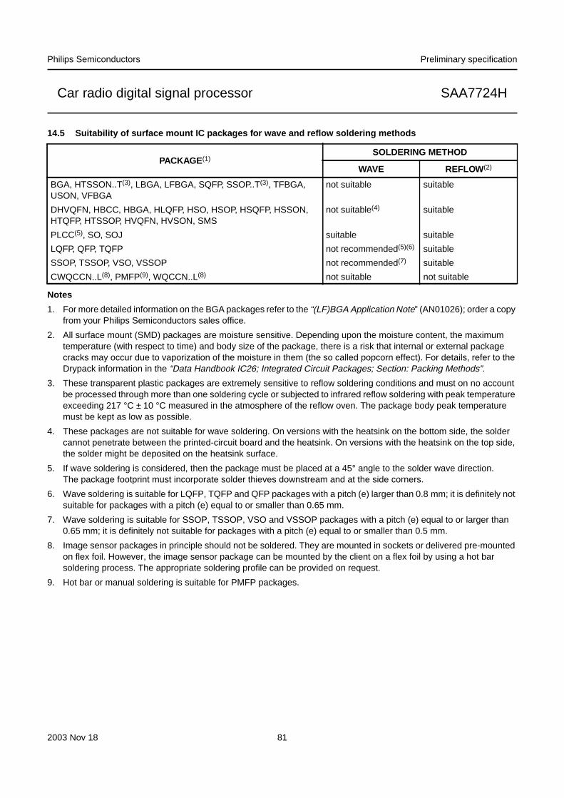
2003 Nov 18 81
Philips Semiconductors Preliminary specification
Car radio digital signal processor SAA7724H
14.5 Suitability of surface mount IC packages for wave and reflow soldering methods
Notes
1. For more detailed information on the BGA packages refer to the “(LF)BGA Application Note” (AN01026); order a copyfrom your Philips Semiconductors sales office.
2. All surface mount (SMD) packages are moisture sensitive. Depending upon the moisture content, the maximumtemperature (with respect to time) and body size of the package, there is a risk that internal or external packagecracks may occur due to vaporization of the moisture in them (the so called popcorn effect). For details, refer to theDrypack information in the “Data Handbook IC26; Integrated Circuit Packages; Section: Packing Methods”.
3. These transparent plastic packages are extremely sensitive to reflow soldering conditions and must on no accountbe processed through more than one soldering cycle or subjected to infrared reflow soldering with peak temperatureexceeding 217 °C ± 10 °C measured in the atmosphere of the reflow oven. The package body peak temperaturemust be kept as low as possible.
4. These packages are not suitable for wave soldering. On versions with the heatsink on the bottom side, the soldercannot penetrate between the printed-circuit board and the heatsink. On versions with the heatsink on the top side,the solder might be deposited on the heatsink surface.
5. If wave soldering is considered, then the package must be placed at a 45° angle to the solder wave direction.The package footprint must incorporate solder thieves downstream and at the side corners.
6. Wave soldering is suitable for LQFP, TQFP and QFP packages with a pitch (e) larger than 0.8 mm; it is definitely notsuitable for packages with a pitch (e) equal to or smaller than 0.65 mm.
7. Wave soldering is suitable for SSOP, TSSOP, VSO and VSSOP packages with a pitch (e) equal to or larger than0.65 mm; it is definitely not suitable for packages with a pitch (e) equal to or smaller than 0.5 mm.
8. Image sensor packages in principle should not be soldered. They are mounted in sockets or delivered pre-mountedon flex foil. However, the image sensor package can be mounted by the client on a flex foil by using a hot barsoldering process. The appropriate soldering profile can be provided on request.
9. Hot bar or manual soldering is suitable for PMFP packages.
PACKAGE (1)SOLDERING METHOD
WAVE REFLOW (2)
BGA, HTSSON..T(3), LBGA, LFBGA, SQFP, SSOP..T(3), TFBGA,USON, VFBGA
not suitable suitable
DHVQFN, HBCC, HBGA, HLQFP, HSO, HSOP, HSQFP, HSSON,HTQFP, HTSSOP, HVQFN, HVSON, SMS
not suitable(4) suitable
PLCC(5), SO, SOJ suitable suitable
LQFP, QFP, TQFP not recommended(5)(6) suitable
SSOP, TSSOP, VSO, VSSOP not recommended(7) suitable
CWQCCN..L(8), PMFP(9), WQCCN..L(8) not suitable not suitable
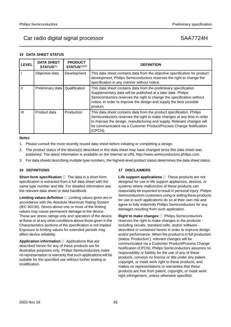
2003 Nov 18 82
Philips Semiconductors Preliminary specification
Car radio digital signal processor SAA7724H
15 DATA SHEET STATUS
Notes
1. Please consult the most recently issued data sheet before initiating or completing a design.
2. The product status of the device(s) described in this data sheet may have changed since this data sheet waspublished. The latest information is available on the Internet at URL http://www.semiconductors.philips.com.
3. For data sheets describing multiple type numbers, the highest-level product status determines the data sheet status.
LEVELDATA SHEET
STATUS(1)PRODUCT
STATUS(2)(3) DEFINITION
I Objective data Development This data sheet contains data from the objective specification for productdevelopment. Philips Semiconductors reserves the right to change thespecification in any manner without notice.
II Preliminary data Qualification This data sheet contains data from the preliminary specification.Supplementary data will be published at a later date. PhilipsSemiconductors reserves the right to change the specification withoutnotice, in order to improve the design and supply the best possibleproduct.
III Product data Production This data sheet contains data from the product specification. PhilipsSemiconductors reserves the right to make changes at any time in orderto improve the design, manufacturing and supply. Relevant changes willbe communicated via a Customer Product/Process Change Notification(CPCN).
16 DEFINITIONS
Short-form specification The data in a short-formspecification is extracted from a full data sheet with thesame type number and title. For detailed information seethe relevant data sheet or data handbook.
Limiting values definition Limiting values given are inaccordance with the Absolute Maximum Rating System(IEC 60134). Stress above one or more of the limitingvalues may cause permanent damage to the device.These are stress ratings only and operation of the deviceat these or at any other conditions above those given in theCharacteristics sections of the specification is not implied.Exposure to limiting values for extended periods mayaffect device reliability.
Application information Applications that aredescribed herein for any of these products are forillustrative purposes only. Philips Semiconductors makeno representation or warranty that such applications will besuitable for the specified use without further testing ormodification.
17 DISCLAIMERS
Life support applications These products are notdesigned for use in life support appliances, devices, orsystems where malfunction of these products canreasonably be expected to result in personal injury. PhilipsSemiconductors customers using or selling these productsfor use in such applications do so at their own risk andagree to fully indemnify Philips Semiconductors for anydamages resulting from such application.
Right to make changes Philips Semiconductorsreserves the right to make changes in the products -including circuits, standard cells, and/or software -described or contained herein in order to improve designand/or performance. When the product is in full production(status ‘Production’), relevant changes will becommunicated via a Customer Product/Process ChangeNotification (CPCN). Philips Semiconductors assumes noresponsibility or liability for the use of any of theseproducts, conveys no licence or title under any patent,copyright, or mask work right to these products, andmakes no representations or warranties that theseproducts are free from patent, copyright, or mask workright infringement, unless otherwise specified.

2003 Nov 18 83
Philips Semiconductors Preliminary specification
Car radio digital signal processor SAA7724H
18 PURCHASE OF PHILIPS I2C COMPONENTS
Purchase of Philips I2C components conveys a license under the Philips’ I2C patent to use thecomponents in the I2C system provided the system conforms to the I2C specification defined byPhilips. This specification can be ordered using the code 9398 393 40011.

© Koninklijke Philips Electronics N.V. 2003 SCA75All rights are reserved. Reproduction in whole or in part is prohibited without the prior written consent of the copyright owner.
The information presented in this document does not form part of any quotation or contract, is believed to be accurate and reliable and may be changedwithout notice. No liability will be accepted by the publisher for any consequence of its use. Publication thereof does not convey nor imply any licenseunder patent- or other industrial or intellectual property rights.
Philips Semiconductors – a worldwide company
Contact information
For additional information please visit http://www.semiconductors.philips.com . Fax: +31 40 27 24825For sales offices addresses send e-mail to: [email protected] .
Printed in The Netherlands 753503/02/pp84 Date of release: 2003 Nov 18 Document order number: 9397 750 11426
Related Documents


![Digital Signal Processor ( DSP ) [French]](https://static.cupdf.com/doc/110x72/55668769d8b42a51558b468d/digital-signal-processor-dsp-french.jpg)

