Rev. 2.00 S1V30080 Series Hardware Specifications

Welcome message from author
This document is posted to help you gain knowledge. Please leave a comment to let me know what you think about it! Share it to your friends and learn new things together.
Transcript
Rev. 2.00
S1V30080 Series Hardware Specifications
NOTICE
No part of this material may be reproduced or duplicated in any form or by any means without the written permission of Seiko Epson. Seiko Epson reserves the right to make changes to this material without notice. Seiko Epson does not assume any liability of any kind arising out of any inaccuracies contained in this material or due to its application or use in any product or circuit and, further, there is no representation that this material is applicable to products requiring high level reliability, such as, medical products. Moreover, no license to any intellectual property rights is granted by implication or otherwise, and there is no representation or warranty that anything made in accordance with this material will be free from any patent or copyright infringement of a third party. This material or portions thereof may contain technology or the subject relating to strategic products under the control of the Foreign Exchange and Foreign Trade Law of Japan and may require an export license from the Ministry of Economy, Trade and Industry or other approval from another government agency. All brands or product names mentioned herein are trademarks and/or registered trademarks of their respective companies.
©SEIKO EPSON CORPORATION 2009, All rights reserved.
S1V30080 Series Hardware Specifications Seiko Epson Corporation i (Rev. 2.00)
Table of Contents
1. Overview............................................................................................................................................ 1
2. Features............................................................................................................................................. 2
3. Product Configuration...................................................................................................................... 3
4. Pin Layout ......................................................................................................................................... 4
4.1 SSOP2-16 (external clock input) ................................................................................................... 4
4.2 SSOP2-16 (oscillator connection) ................................................................................................. 5
4.3 QFP12-48...................................................................................................................................... 6
4.4 QFP13-52 (external clock input).................................................................................................... 7
4.5 QFP13-52 (oscillator connection) .................................................................................................. 8
5. Pin Description ................................................................................................................................. 9
5.1 Pin Description 1 ........................................................................................................................... 9
5.2 Pin Description 2 ......................................................................................................................... 11
6. Function Description ...................................................................................................................... 14
6.1 Standard application system ....................................................................................................... 14
6.2 System clock ............................................................................................................................... 15
6.3 Host interface .............................................................................................................................. 16
7. Electrical Characteristics ............................................................................................................... 17
7.1 Absolute maximum ratings .......................................................................................................... 17
7.2 Recommended operating conditions ........................................................................................... 17
7.3 DC characteristics ....................................................................................................................... 18
7.3.1 DC characteristics with power supply voltage 5.0 V ± 0.5 V ................................................. 18
7.3.2 DC characteristics with power supply voltage 3.3 V ± 0.3 V ................................................. 20
7.3.3 DC characteristics with power supply voltage 2.4 V ± 0.2 V ................................................. 22
7.3.4 Operating power supply current and internal system clock frequency characteristics .......... 24
7.4 AC characteristics........................................................................................................................ 25
7.4.1 System clock timing .............................................................................................................. 25
7.4.2 Power on/reset timing ........................................................................................................... 26
7.4.3 Command receipt timing....................................................................................................... 27
7.4.4 Standalone mode control timing............................................................................................ 28
7.4.5 Initialization timing from external serial flash memory........................................................... 29
7.4.6 Serial host interface (SPI) ..................................................................................................... 30
7.4.7 Serial host interface (I2C) ..................................................................................................... 31
7.4.8 MSG_RECEIVE output......................................................................................................... 32
7.4.9 SOUND_PLAYING output..................................................................................................... 33
7.4.10 External serial flash memory access timing........................................................................ 34
7.4.11 Power supply disconnection timing ..................................................................................... 35
ii Seiko Epson Corporation S1V30080 Series Hardware Specifications (Rev. 2.00)
7.4.12 Sleep mode start timing using CE pin................................................................................. 36
8. External Connection Examples ..................................................................................................... 37
8.1 System clock ............................................................................................................................... 37
8.1.1 Direct input............................................................................................................................ 37
8.1.2 Oscillator............................................................................................................................... 38
8.2 Serial host interface..................................................................................................................... 40
8.2.1 SPI........................................................................................................................................ 40
8.2.2 I2C ........................................................................................................................................ 41
8.3 Standalone connection ................................................................................................................ 42
8.4 External serial flash memory interface ........................................................................................ 43
8.5 Sleep mode control using CE pin ................................................................................................ 44
9. Package Information....................................................................................................................... 45
9.1 SSOP2-16 ................................................................................................................................... 45
9.2 QFP12-48.................................................................................................................................... 46
9.3 QFP13-52.................................................................................................................................... 47
10. Reference Material ........................................................................................................................ 48
10.1 Practical circuit example (SSOP2-16) ....................................................................................... 48
10.2 Practical circuit example (QFP12-48/13-52).............................................................................. 49
10.3 Practical circuit example (Audio output section) ........................................................................ 50
10.4 Mute start/cancel timing ............................................................................................................ 51
10.5 Precautions concerning power supply....................................................................................... 52
10.6 Clock direct input precautions ................................................................................................... 53
10.7 Mounting precautions ................................................................................................................ 54
10.7.1 Oscillator circuit .................................................................................................................. 54
10.7.2 Reset circuit ........................................................................................................................ 55
10.7.3 Power supply ...................................................................................................................... 55
10.7.4 Signal line location.............................................................................................................. 55
10.7.5 Malfunction due to noise..................................................................................................... 56
10.7.6 Miscellaneous ..................................................................................................................... 56
10.8 Product code scheme................................................................................................................ 57
Revision History ................................................................................................................................. 58
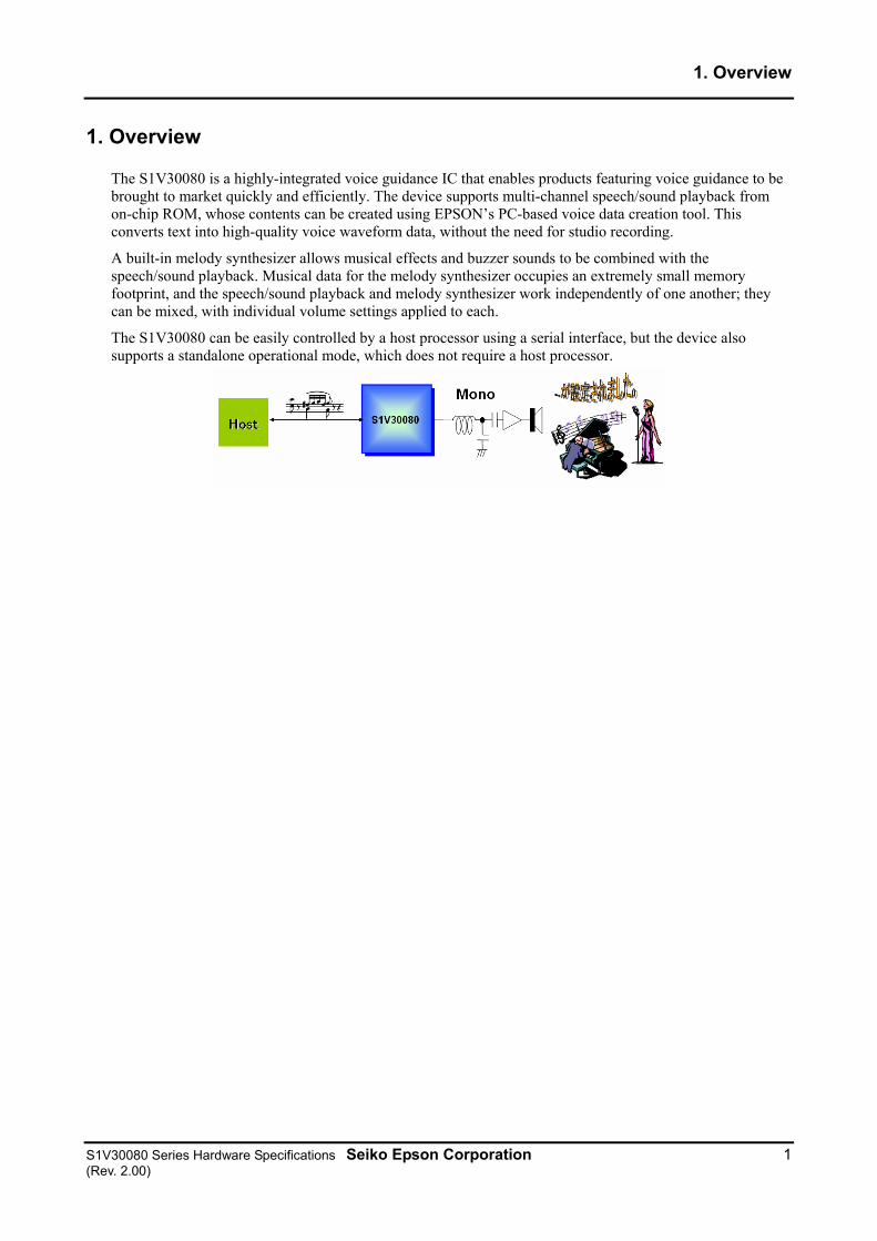
1. Overview
S1V30080 Series Hardware Specifications Seiko Epson Corporation 1 (Rev. 2.00)
1. Overview
The S1V30080 is a highly-integrated voice guidance IC that enables products featuring voice guidance to be brought to market quickly and efficiently. The device supports multi-channel speech/sound playback from on-chip ROM, whose contents can be created using EPSON’s PC-based voice data creation tool. This converts text into high-quality voice waveform data, without the need for studio recording.
A built-in melody synthesizer allows musical effects and buzzer sounds to be combined with the speech/sound playback. Musical data for the melody synthesizer occupies an extremely small memory footprint, and the speech/sound playback and melody synthesizer work independently of one another; they can be mixed, with individual volume settings applied to each.
The S1V30080 can be easily controlled by a host processor using a serial interface, but the device also supports a standalone operational mode, which does not require a host processor.
2. Features
2 Seiko Epson Corporation S1V30080 Series Hardware Specifications (Rev. 2.00)
2. Features
Melody/Buzzer/Tone synthesizer function - 5-channel melody sound can be created from music note information (5-octave range supported). - Buzzer/tone sounds can be generated simply by specifying the frequency (5 channels supported).
Speech/Sound playback - Individual 2ch Voice ROM data can be played (Epson original data format). - Sampling Frequency: 4, 8, 12, 16 kHz
Sequencer function (to set delay between phrases) - Up to 127 files can be sequenced with one configuration message (no constraints on phrase
combinations). - Delay setting can be set between phrases: 0 - 1,000 ms (in 10 ms steps)
Mixing function - Synthesizer and speech/sound playback from ROM can be mixed (individual volume settings
supported).
Internal voice data ROM - fs 8 kHz: approx. 30 sec, fs 16 kHz: approx. 15 sec
External serial flash memory access - External serial flash memory access possible with package option. (S1V30080F00**00 and
S1V30080F10**00)
Serial host interface - Synchronous serial interface (SPI, I2C) (command control)
Standalone mode - Simply by specifying the sound file number, the sound can be played from ROM or the melody
synthesizer.
Internal DA converter clock (external clock input/crystal oscillator/ceramic oscillator) - fs 8 kHz: 8.192 MHz, fs 16 kHz: 16.384 MHz
Package - SSOP-16-pin (4.4 mm x 6.6 mm, 0.8 mm pin pitch) - QFP-48-pin (7 mm x 7 mm, 0.5 mm pin pitch): Supports external serial flash memory - QFP-52-pin (10 mm x 10mm, 0.65mm pin pitch): Supports external serial flash memory
(S1V30080F10**00 only)
Power supply voltage - 2.2 - 5.5 V single power supply
3. Product Configuration
S1V30080 Series Hardware Specifications Seiko Epson Corporation 3 (Rev. 2.00)
3. Product Configuration
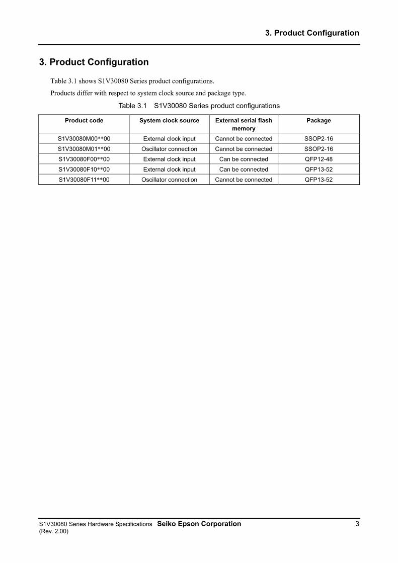
Table 3.1 shows S1V30080 Series product configurations.
Products differ with respect to system clock source and package type.
Table 3.1 S1V30080 Series product configurations
Product code System clock source External serial flash memory
Package
S1V30080M00**00 External clock input Cannot be connected SSOP2-16
S1V30080M01**00 Oscillator connection Cannot be connected SSOP2-16
S1V30080F00**00 External clock input Can be connected QFP12-48
S1V30080F10**00 External clock input Can be connected QFP13-52
S1V30080F11**00 Oscillator connection Cannot be connected QFP13-52
4. Pin Layout
4 Seiko Epson Corporation S1V30080 Series Hardware Specifications (Rev. 2.00)
4. Pin Layout
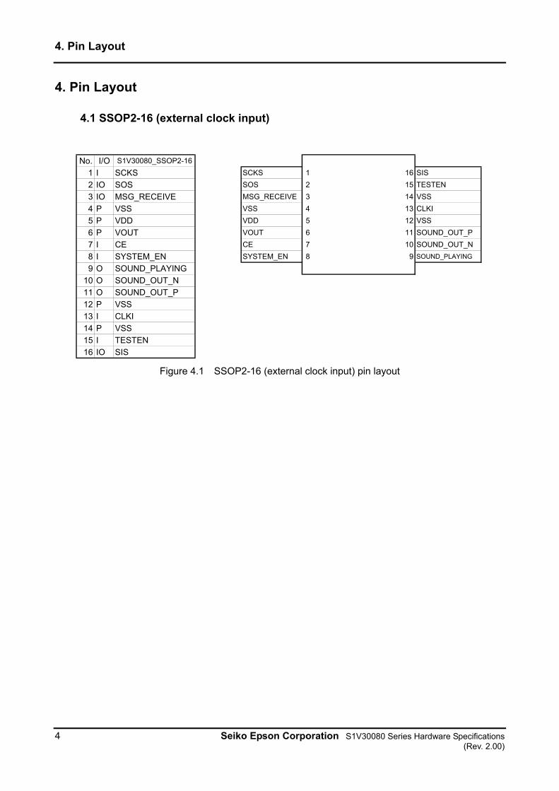
4.1 SSOP2-16 (external clock input)
No. I/O S1V30080_SSOP2-16
1 I SCKS SCKS 1 16 SIS
2 IO SOS SOS 2 15 TESTEN
3 IO MSG_RECEIVE MSG_RECEIVE 3 14 VSS
4 P VSS VSS 4 13 CLKI
5 P VDD VDD 5 12 VSS
6 P VOUT VOUT 6 11 SOUND_OUT_P
7 I CE CE 7 10 SOUND_OUT_N
8 I SYSTEM_EN SYSTEM_EN 8 9 SOUND_PLAYING
9 O SOUND_PLAYING
10 O SOUND_OUT_N
11 O SOUND_OUT_P
12 P VSS
13 I CLKI
14 P VSS
15 I TESTEN
16 IO SIS
Figure 4.1 SSOP2-16 (external clock input) pin layout
4. Pin Layout
S1V30080 Series Hardware Specifications Seiko Epson Corporation 5 (Rev. 2.00)
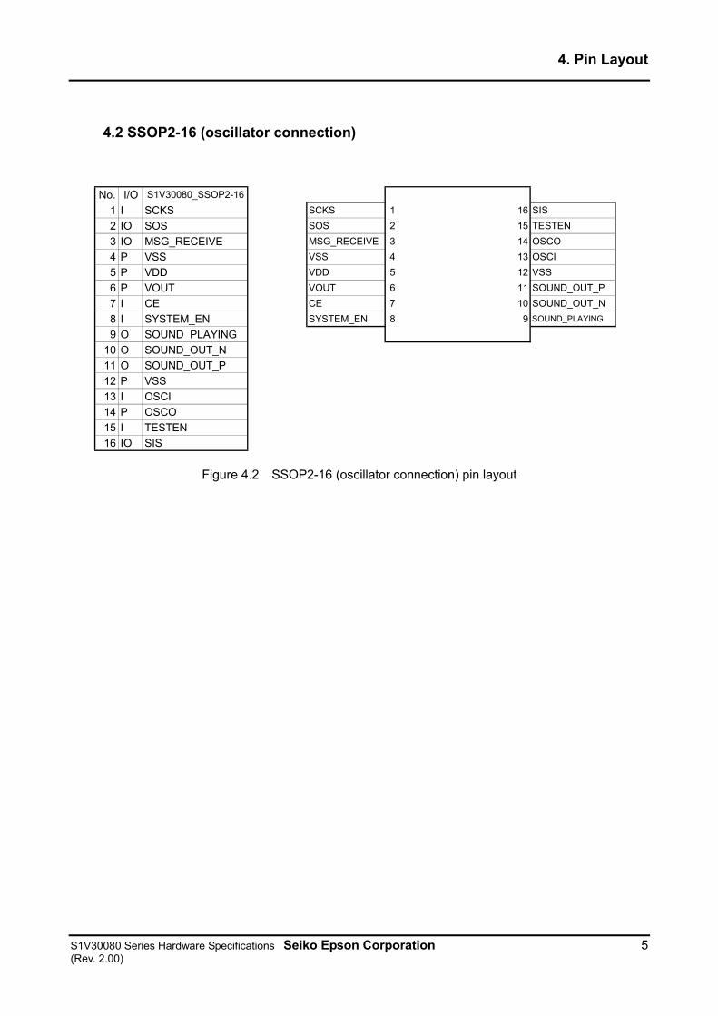
4.2 SSOP2-16 (oscillator connection)
No. I/O S1V30080_SSOP2-16
1 I SCKS SCKS 1 16 SIS
2 IO SOS SOS 2 15 TESTEN
3 IO MSG_RECEIVE MSG_RECEIVE 3 14 OSCO
4 P VSS VSS 4 13 OSCI
5 P VDD VDD 5 12 VSS
6 P VOUT VOUT 6 11 SOUND_OUT_P
7 I CE CE 7 10 SOUND_OUT_N
8 I SYSTEM_EN SYSTEM_EN 8 9 SOUND_PLAYING
9 O SOUND_PLAYING
10 O SOUND_OUT_N
11 O SOUND_OUT_P
12 P VSS
13 I OSCI
14 P OSCO
15 I TESTEN
16 IO SIS
Figure 4.2 SSOP2-16 (oscillator connection) pin layout
4. Pin Layout
6 Seiko Epson Corporation S1V30080 Series Hardware Specifications (Rev. 2.00)
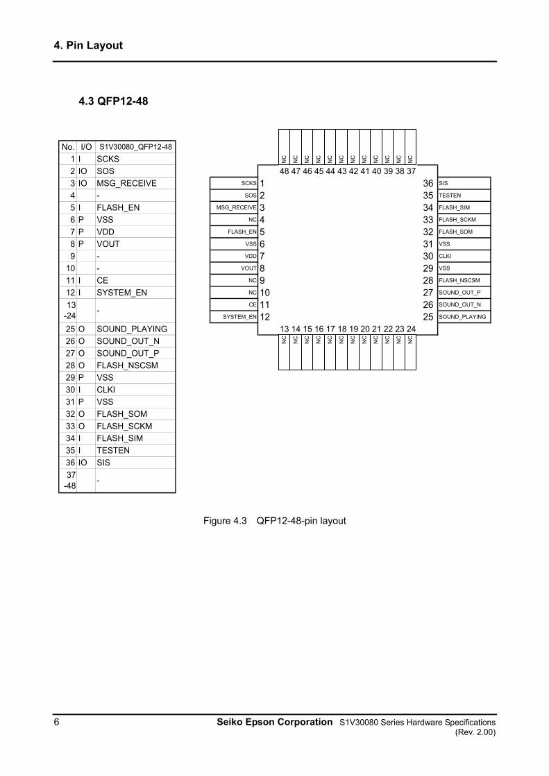
4.3 QFP12-48
No. I/O S1V30080_QFP12-48
1 I SCKS
2 IO SOS 48 47 46 45 44 43 42 41 40 39 38 37
3 IO MSG_RECEIVE SCKS 1 36 SIS
4 - SOS 2 35 TESTEN
5 I FLASH_EN MSG_RECEIVE 3 34 FLASH_SIM
6 P VSS NC 4 33 FLASH_SCKM
7 P VDD FLASH_EN 5 32 FLASH_SOM
8 P VOUT VSS 6 31 VSS
9 - VDD 7 30 CLKI
10 - VOUT 8 29 VSS
11 I CE NC 9 28 FLASH_NSCSM
12 I SYSTEM_EN NC 10 27 SOUND_OUT_P
CE 11 26 SOUND_OUT_N
SYSTEM_EN 12 25 SOUND_PLAYING
25 O SOUND_PLAYING 13 14 15 16 17 18 19 20 21 22 23 24
26 O SOUND_OUT_N
27 O SOUND_OUT_P
28 O FLASH_NSCSM
29 P VSS
30 I CLKI
31 P VSS
32 O FLASH_SOM
33 O FLASH_SCKM
34 I FLASH_SIM
35 I TESTEN
36 IO SIS
37-48
-
13-24
-
NC
NC
NC
NC
NC
NC
NC
NC
NC
NC
NC
NC
NC
NC
NC
NC
NC
NC
NC
NC
NC
NC
NC
NC
Figure 4.3 QFP12-48-pin layout
4. Pin Layout
S1V30080 Series Hardware Specifications Seiko Epson Corporation 7 (Rev. 2.00)
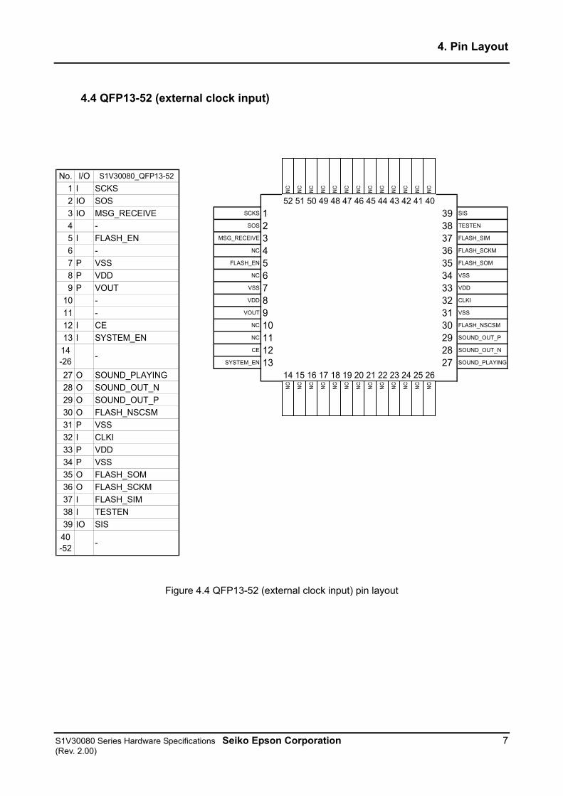
4.4 QFP13-52 (external clock input)
No. I/O S1V30080_QFP13-52
1 I SCKS
2 IO SOS 52 51 50 49 48 47 46 45 44 43 42 41 40
3 IO MSG_RECEIVE SCKS 1 39 SIS
4 - SOS 2 38 TESTEN
5 I FLASH_EN MSG_RECEIVE 3 37 FLASH_SIM
6 - NC 4 36 FLASH_SCKM
7 P VSS FLASH_EN 5 35 FLASH_SOM
8 P VDD NC 6 34 VSS
9 P VOUT VSS 7 33 VDD
10 - VDD 8 32 CLKI
11 - VOUT 9 31 VSS
12 I CE NC 10 30 FLASH_NSCSM
13 I SYSTEM_EN NC 11 29 SOUND_OUT_P
CE 12 28 SOUND_OUT_N
SYSTEM_EN 13 27 SOUND_PLAYING
27 O SOUND_PLAYING 14 15 16 17 18 19 20 21 22 23 24 25 26
28 O SOUND_OUT_N
29 O SOUND_OUT_P
30 O FLASH_NSCSM
31 P VSS
32 I CLKI
33 P VDD
34 P VSS
35 O FLASH_SOM
36 O FLASH_SCKM
37 I FLASH_SIM
38 I TESTEN
39 IO SIS
40-52
-
14-26
-
NC
NC
NC
NC
NC
NC
NC
NC
NC
NC
NC
NC
NC
NC
NC
NC
NC
NC
NC
NC
NC
NC
NC
NC
NC
NC
Figure 4.4 QFP13-52 (external clock input) pin layout
4. Pin Layout
8 Seiko Epson Corporation S1V30080 Series Hardware Specifications (Rev. 2.00)
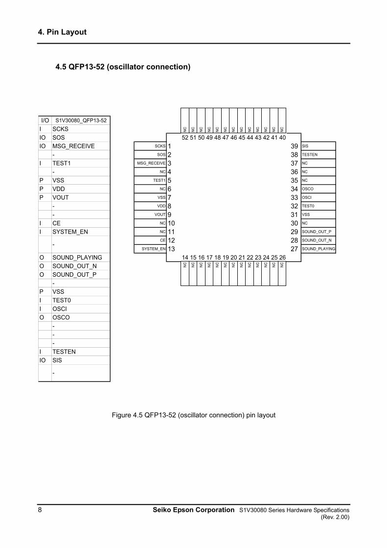
4.5 QFP13-52 (oscillator connection)
I/O S1V30080_QFP13-52
I SCKS
IO SOS 52 51 50 49 48 47 46 45 44 43 42 41 40
IO MSG_RECEIVE SCKS 1 39 SIS
- SOS 2 38 TESTEN
I TEST1 MSG_RECEIVE 3 37 NC
- NC 4 36 NC
P VSS TEST1 5 35 NC
P VDD NC 6 34 OSCO
P VOUT VSS 7 33 OSCI
- VDD 8 32 TEST0
- VOUT 9 31 VSS
I CE NC 10 30 NC
I SYSTEM_EN NC 11 29 SOUND_OUT_P
CE 12 28 SOUND_OUT_N
SYSTEM_EN 13 27 SOUND_PLAYING
O SOUND_PLAYING 14 15 16 17 18 19 20 21 22 23 24 25 26
O SOUND_OUT_N
O SOUND_OUT_P
-
P VSS
I TEST0
I OSCI
O OSCO
-
-
-
I TESTEN
IO SIS
-
-
NC
NC
NC
NC
NC
NC
NC
NC
NC
NC
NC
NC
NC
NC
NC
NC
NC
NC
NC
NC
NC
NC
NC
NC
NC
NC
Figure 4.5 QFP13-52 (oscillator connection) pin layout
5. Pin Description
S1V30080 Series Hardware Specifications Seiko Epson Corporation 9 (Rev. 2.00)
5. Pin Description
Key I: Input pin O: Output pin IO: Bidirectional pin P: Power supply pin Z: High impedance
I/O cell types
Code Function
IC LVCMOS input
IH LVCMOS Schmitt input
O1 Output buffer (output current 2.0 mA / -2.0 mA @5.0 V (typ.))
O2 Output buffer (output current 4.0 mA / -4.0 mA @5.0 V (typ.))
T1 3-state output buffer (output current 2.0 mA / -2.0 mA @5.0 V (typ.))
BC1 Bidirectional buffer (output current 2.0 mA / -2.0 mA @5.0 V (typ.))
BH1 Bidirectional buffer Schmitt input (output current 2.0 mA / -2.0 mA @5.0 V (typ.))
LLIN Transparent input (1.8 V)
LLOT Transparent output (1.8 V)
HLIN Transparent input (VDD)
ITST1 Test input with pull-down resistance (120 kΩ @ 1.8 V (typ.))
5.1 Pin Description 1 Package types
PKG1: SSOP2-16 (external clock input) PKG2: SSOP2-16 (oscillator connection) PKG3: QFP12-48
Pin name
(SPI/
I2C/
Standalone)
PKG
1
PKG
2
PKG
3 I/O
I/O
cell type
State when
SYSTEM_EN=L
State
when
CE=L
I/O
power
supply
Function
Host interface
SIS/
SDA/
SET_PLAY0
16 16 36 IO BH1 Z Z VDD
[SPI] Serial data input
[I2C] Data input/output
[Standalone] SET_PLAY0
SCKS/
SCL/
SET_PLAY1
1 1 1 I IH1 Z Z VDD
[SPI] Serial clock input
[I2C] Serial clock input
[Standalone] SET_PLAY1
SOS/
-/
SET_PLAY2
2 2 2 IO BH1 Z Z VDD
[SPI] Serial data output
[I2C] Fixed to Low externally
[Standalone] SET_PLAY2
MSG_RECEIVE/
MSG_RECEIVE/
SET_PLAY3
3 3 3 IO BH1 Z Z VDD
[SPI] Serial data receipt ended
[I2C] Serial data receipt ended
[Standalone] SET_PLAY3
SOUND_PLAYING 9 9 25 O O1 L Z VDD Sound output interval output
5. Pin Description
10 Seiko Epson Corporation S1V30080 Series Hardware Specifications (Rev. 2.00)
Pin name PKG
1
PKG
2
PKG
3 I/O
I/O cell
type
State when
SYSTEM_EN = L
State
when
CE = L
I/O
power
supply
Function
Audio output
SOUND_OUT_P 11 11 27 O O2 L Z VDD Sound output (positive phase)
SOUND_OUT_N 10 10 26 O O2 L Z VDD Sound output (negative phase)
System clock
CLKI 13 - 30 I IH Z Z VDD Clock input (refer to Section 6.2)
OSCI - 13 - I LLIN Z Z - Oscillator connector pin
(refer to Section 6.2)
OSCO - 14 - O LLOT - - - Oscillator connector pin
(refer to Section 6.2)
System control
CE 7 7 11 I HLIN Z - VDD Internal stepdown regulator
Operating (H)/Stopped (L)
SYSTEM_EN 8 8 12 I IH - Z VDD System operation (H)/
Stopped (L)
Test input/output
TESTEN 15 15 35 I ITST1 Pull-down Pull-down - Test mode control pin
(Normally fixed to Low)
External serial flash memory control
FLASH_EN - - 5 I IH Z Z VDD External serial flash read
access enable
FLASH_SCKM - - 33 O T1 Z Z VDD External serial flash clock
output
FLASH_NSCSM - - 28 O T1 Z Z VDD External serial flash slave
selection output
FLASH_SIM - - 34 I IH Z Z VDD External serial flash data input
FLASH_SOM - - 32 O T1 Z Z VDD External serial flash data output
(Continued on next page)
5. Pin Description
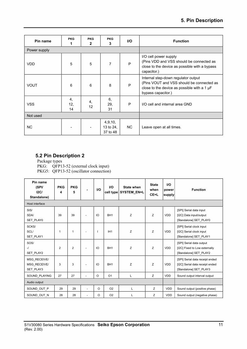
S1V30080 Series Hardware Specifications Seiko Epson Corporation 11 (Rev. 2.00)
Pin name PKG
1 PKG
2 PKG
3 I/O Function
Power supply
VDD 5 5 7 P
I/O cell power supply (Pins VDD and VSS should be connected as close to the device as possible with a bypass capacitor.)
VOUT 6 6 8 P
Internal step-down regulator output (Pins VOUT and VSS should be connected as close to the device as possible with a 1 µF bypass capacitor.)
VSS 4, 12, 14
4, 12
6, 29, 31
P I/O cell and internal area GND
Not used
NC - - 4,9,10,
13 to 24,37 to 48
NC Leave open at all times.
5.2 Pin Description 2 Package types PKG: QFP13-52 (external clock input) PKG5: QFP13-52 (oscillator connection)
Pin name
(SPI/
I2C/
Standalone)
PKG
4
PKG
5 - I/O
I/O
cell type
State when
SYSTEM_EN=L
State
when
CE=L
I/O
power
supply
Function
Host interface
SIS/
SDA/
SET_PLAY0
39 39 - IO BH1 Z Z VDD
[SPI] Serial data input
[I2C] Data input/output
[Standalone] SET_PLAY0
SCKS/
SCL/
SET_PLAY1
1 1 - I IH1 Z Z VDD
[SPI] Serial clock input
[I2C] Serial clock input
[Standalone] SET_PLAY1
SOS/
-/
SET_PLAY2
2 2 - IO BH1 Z Z VDD
[SPI] Serial data output
[I2C] Fixed to Low externally
[Standalone] SET_PLAY2
MSG_RECEIVE/
MSG_RECEIVE/
SET_PLAY3
3 3 - IO BH1 Z Z VDD
[SPI] Serial data receipt ended
[I2C] Serial data receipt ended
[Standalone] SET_PLAY3
SOUND_PLAYING 27 27 - O O1 L Z VDD Sound output interval output
Audio output
SOUND_OUT_P 29 29 - O O2 L Z VDD Sound output (positive phase)
SOUND_OUT_N 28 28 - O O2 L Z VDD Sound output (negative phase)
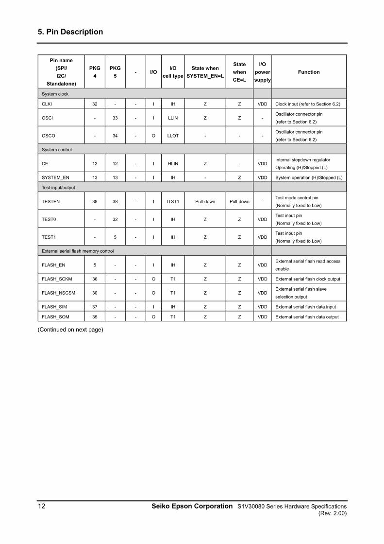
5. Pin Description
12 Seiko Epson Corporation S1V30080 Series Hardware Specifications (Rev. 2.00)
Pin name
(SPI/
I2C/
Standalone)
PKG
4
PKG
5 - I/O
I/O
cell type
State when
SYSTEM_EN=L
State
when
CE=L
I/O
power
supply
Function
System clock
CLKI 32 - - I IH Z Z VDD Clock input (refer to Section 6.2)
OSCI - 33 - I LLIN Z Z - Oscillator connector pin
(refer to Section 6.2)
OSCO - 34 - O LLOT - - - Oscillator connector pin
(refer to Section 6.2)
System control
CE 12 12 - I HLIN Z - VDDInternal stepdown regulator
Operating (H)/Stopped (L)
SYSTEM_EN 13 13 - I IH - Z VDD System operation (H)/Stopped (L)
Test input/output
TESTEN 38 38 - I ITST1 Pull-down Pull-down - Test mode control pin
(Normally fixed to Low)
TEST0 - 32 - I IH Z Z VDDTest input pin
(Normally fixed to Low)
TEST1 - 5 - I IH Z Z VDDTest input pin
(Normally fixed to Low)
External serial flash memory control
FLASH_EN 5 - - I IH Z Z VDDExternal serial flash read access
enable
FLASH_SCKM 36 - - O T1 Z Z VDD External serial flash clock output
FLASH_NSCSM 30 - - O T1 Z Z VDDExternal serial flash slave
selection output
FLASH_SIM 37 - - I IH Z Z VDD External serial flash data input
FLASH_SOM 35 - - O T1 Z Z VDD External serial flash data output
(Continued on next page)
5. Pin Description
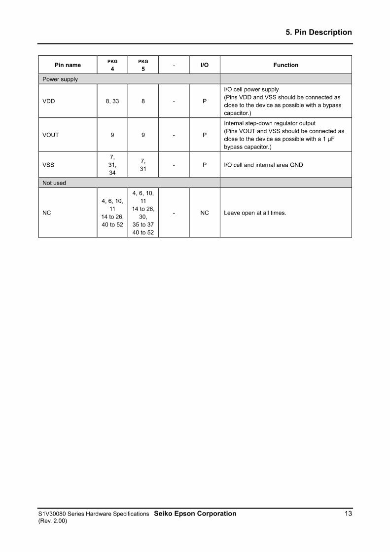
S1V30080 Series Hardware Specifications Seiko Epson Corporation 13 (Rev. 2.00)
Pin name PKG
4 PKG
5 - I/O Function
Power supply
VDD 8, 33 8 - P
I/O cell power supply (Pins VDD and VSS should be connected as close to the device as possible with a bypass capacitor.)
VOUT 9 9 - P
Internal step-down regulator output (Pins VOUT and VSS should be connected as close to the device as possible with a 1 µF bypass capacitor.)
VSS 7, 31, 34
7, 31
- P I/O cell and internal area GND
Not used
NC
4, 6, 10, 11
14 to 26, 40 to 52
4, 6, 10, 11
14 to 26, 30,
35 to 37 40 to 52
- NC Leave open at all times.
6. Function Description
14 Seiko Epson Corporation S1V30080 Series Hardware Specifications (Rev. 2.00)
6. Function Description
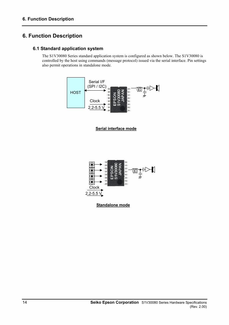
6.1 Standard application system
The S1V30080 Series standard application system is configured as shown below. The S1V30080 is controlled by the host using commands (message protocol) issued via the serial interface. Pin settings also permit operations in standalone mode.
Standalone mode
Clock
2.2-5.5 V
Serial interface mode
HOST
Clock
Serial I/F (SPI / I2C)
2.2-5.5 V
6. Function Description
S1V30080 Series Hardware Specifications Seiko Epson Corporation 15 (Rev. 2.00)
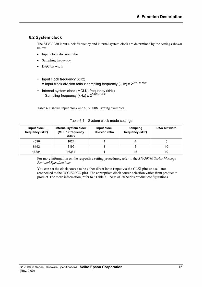
6.2 System clock
The S1V30080 input clock frequency and internal system clock are determined by the settings shown below.
Input clock division ratio
Sampling frequency
DAC bit width
Input clock frequency (kHz) = Input clock division ratio x sampling frequency (kHz) x 2DAC bit width
Internal system clock (MCLK) frequency (kHz) = Sampling frequency (kHz) x 2DAC bit width
Table 6.1 shows input clock and S1V30080 setting examples.
Table 6.1 System clock mode settings
Input clock frequency (kHz)
Internal system clock (MCLK) frequency
(kHz)
Input clock division ratio
Sampling frequency (kHz)
DAC bit width
4096 1024 4 4 8
8192 8192 1 8 10
16384 16384 1 16 10
For more information on the respective setting procedures, refer to the S1V30080 Series Message Protocol Specifications.
You can set the clock source to be either direct input (input via the CLKI pin) or oscillator (connected to the OSCI/OSCO pin). The appropriate clock source selection varies from product to product. For more information, refer to “Table 3.1 S1V30080 Series product configurations.”
6. Function Description
16 Seiko Epson Corporation S1V30080 Series Hardware Specifications (Rev. 2.00)
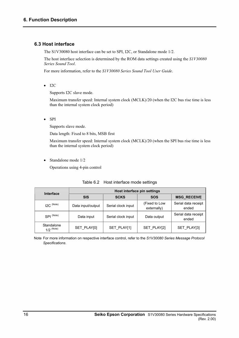
6.3 Host interface
The S1V30080 host interface can be set to SPI, I2C, or Standalone mode 1/2.
The host interface selection is determined by the ROM data settings created using the S1V30080 Series Sound Tool.
For more information, refer to the S1V30080 Series Sound Tool User Guide.
I2C
Supports I2C slave mode.
Maximum transfer speed: Internal system clock (MCLK)/20 (when the I2C bus rise time is less than the internal system clock period)
SPI
Supports slave mode.
Data length: Fixed to 8 bits, MSB first
Maximum transfer speed: Internal system clock (MCLK)/20 (when the SPI bus rise time is less than the internal system clock period)
Standalone mode 1/2
Operations using 4-pin control
Table 6.2 Host interface mode settings
Host interface pin settings Interface
SIS SCKS SOS MSG_RECEIVE
I2C (Note) Data input/output Serial clock input(Fixed to Low
externally) Serial data receipt
ended
SPI (Note) Data input Serial clock input Data output Serial data receipt
ended
Standalone 1/2 (Note)
SET_PLAY[0] SET_PLAY[1] SET_PLAY[2] SET_PLAY[3]
Note For more information on respective interface control, refer to the S1V30080 Series Message Protocol Specifications.
7. Electrical Characteristics
S1V30080 Series Hardware Specifications Seiko Epson Corporation 17 (Rev. 2.00)
7. Electrical Characteristics
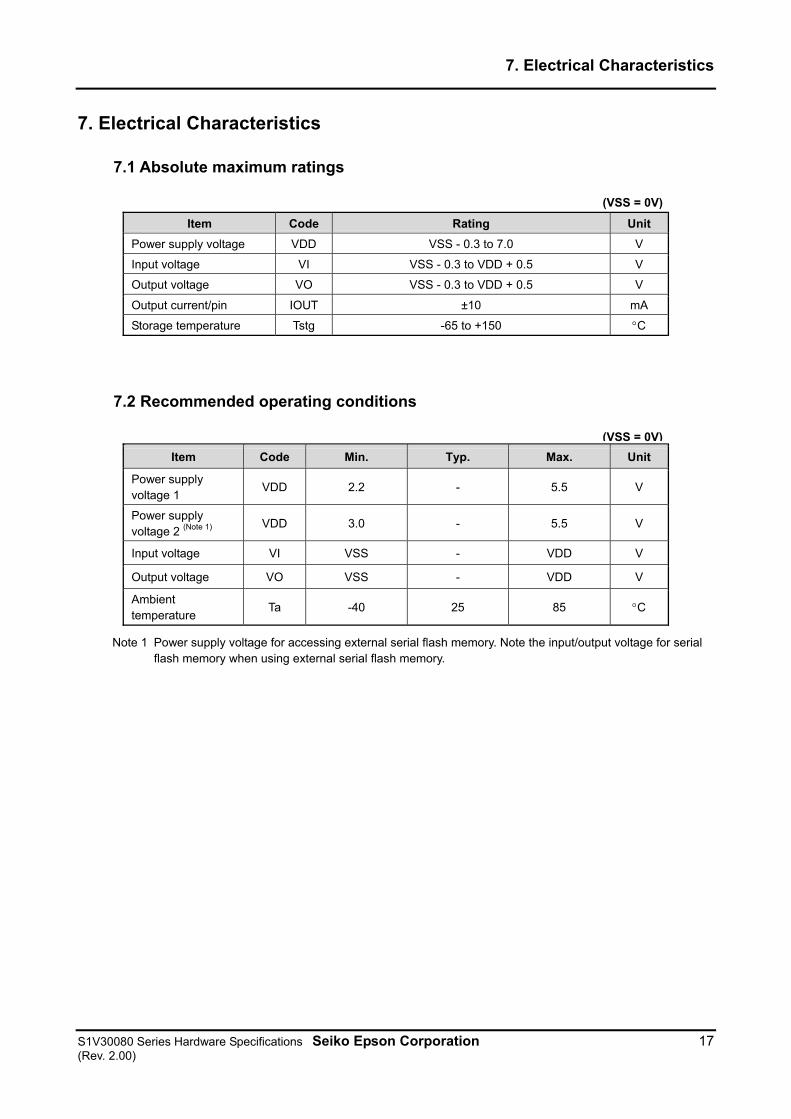
7.1 Absolute maximum ratings
(VSS = 0V)
Item Code Rating Unit
Power supply voltage VDD VSS - 0.3 to 7.0 V
Input voltage VI VSS - 0.3 to VDD + 0.5 V
Output voltage VO VSS - 0.3 to VDD + 0.5 V
Output current/pin IOUT ±10 mA
Storage temperature Tstg -65 to +150 C
7.2 Recommended operating conditions
(VSS = 0V)
Item Code Min. Typ. Max. Unit
Power supply voltage 1
VDD 2.2 - 5.5 V
Power supply voltage 2 (Note 1)
VDD 3.0 - 5.5 V
Input voltage VI VSS - VDD V
Output voltage VO VSS - VDD V
Ambient temperature
Ta -40 25 85 C
Note 1 Power supply voltage for accessing external serial flash memory. Note the input/output voltage for serial flash memory when using external serial flash memory.
7. Electrical Characteristics
18 Seiko Epson Corporation S1V30080 Series Hardware Specifications (Rev. 2.00)
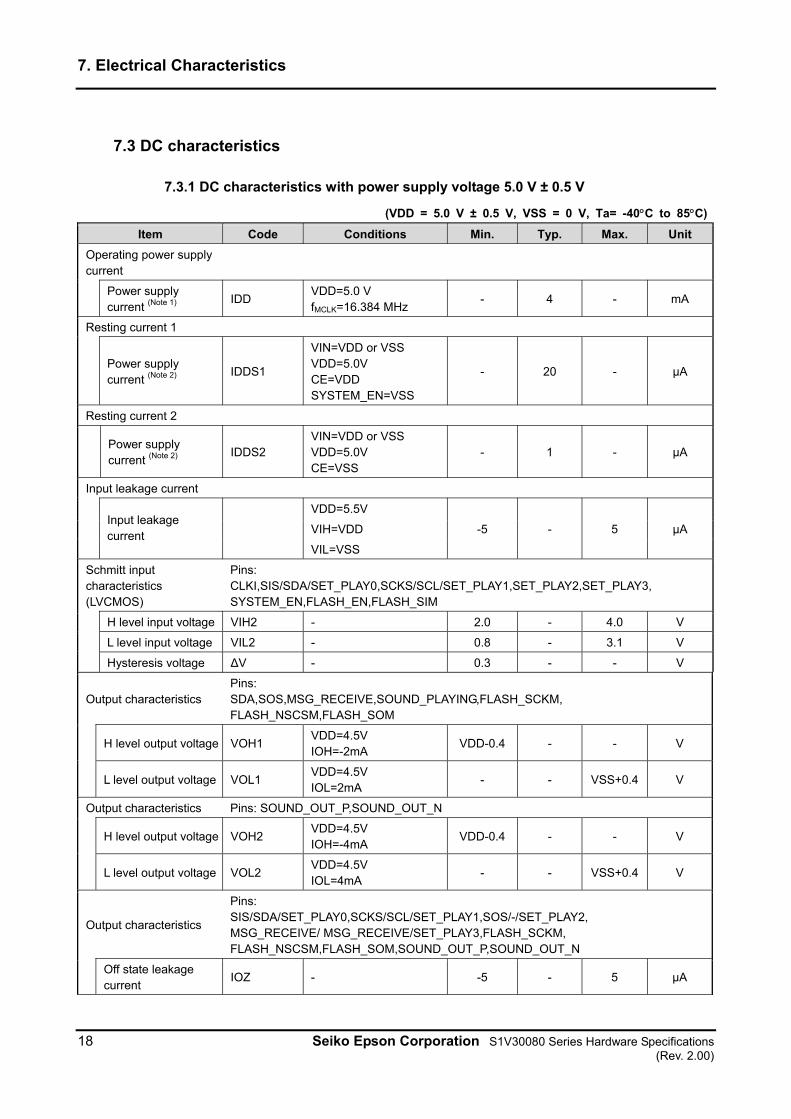
7.3 DC characteristics
7.3.1 DC characteristics with power supply voltage 5.0 V ± 0.5 V
(VDD = 5.0 V ± 0.5 V, VSS = 0 V, Ta= -40C to 85C)
Item Code Conditions Min. Typ. Max. Unit
Operating power supply current
Power supply current (Note 1)
IDD VDD=5.0 V fMCLK=16.384 MHz
- 4 - mA
Resting current 1
Power supply current (Note 2)
IDDS1
VIN=VDD or VSS VDD=5.0V CE=VDD SYSTEM_EN=VSS
- 20 - μA
Resting current 2
Power supply current (Note 2)
IDDS2 VIN=VDD or VSS VDD=5.0V CE=VSS
- 1 - μA
Input leakage current
VDD=5.5V
VIH=VDD -5 - 5 μA
Input leakage current
VIL=VSS
Schmitt input characteristics (LVCMOS)
Pins: CLKI,SIS/SDA/SET_PLAY0,SCKS/SCL/SET_PLAY1,SET_PLAY2,SET_PLAY3, SYSTEM_EN,FLASH_EN,FLASH_SIM
H level input voltage VIH2 - 2.0 - 4.0 V
L level input voltage VIL2 - 0.8 - 3.1 V
Hysteresis voltage ΔV - 0.3 - - V
Output characteristics Pins: SDA,SOS,MSG_RECEIVE,SOUND_PLAYING,FLASH_SCKM, FLASH_NSCSM,FLASH_SOM
H level output voltage VOH1 VDD=4.5V IOH=-2mA
VDD-0.4 - - V
L level output voltage VOL1 VDD=4.5V IOL=2mA
- - VSS+0.4 V
Output characteristics Pins: SOUND_OUT_P,SOUND_OUT_N
H level output voltage VOH2 VDD=4.5V IOH=-4mA
VDD-0.4 - - V
L level output voltage VOL2 VDD=4.5V IOL=4mA
- - VSS+0.4 V
Output characteristics
Pins: SIS/SDA/SET_PLAY0,SCKS/SCL/SET_PLAY1,SOS/-/SET_PLAY2, MSG_RECEIVE/ MSG_RECEIVE/SET_PLAY3,FLASH_SCKM, FLASH_NSCSM,FLASH_SOM,SOUND_OUT_P,SOUND_OUT_N
Off state leakage current
IOZ - -5 - 5 μA
7. Electrical Characteristics
S1V30080 Series Hardware Specifications Seiko Epson Corporation 19 (Rev. 2.00)
Pin capacitance Pins: All input pins
Input pin capacitance
CI f=1MHz VDD=0V
- - 8 pF
Pin capacitance Pins: All output pins
Output pin capacitance
CO f=1MHz VDD=0V
- - 8 pF
Pin capacitance Pins: All input/output pins
Input/output pin capacitance
CIO f=1MHz VDD=0V
- - 8 pF
Output pin permissible load capacitance
Pins: FLASH_SCKM,FLASH_SOM,FLASH_NSCSM
CL - - - 8 pF
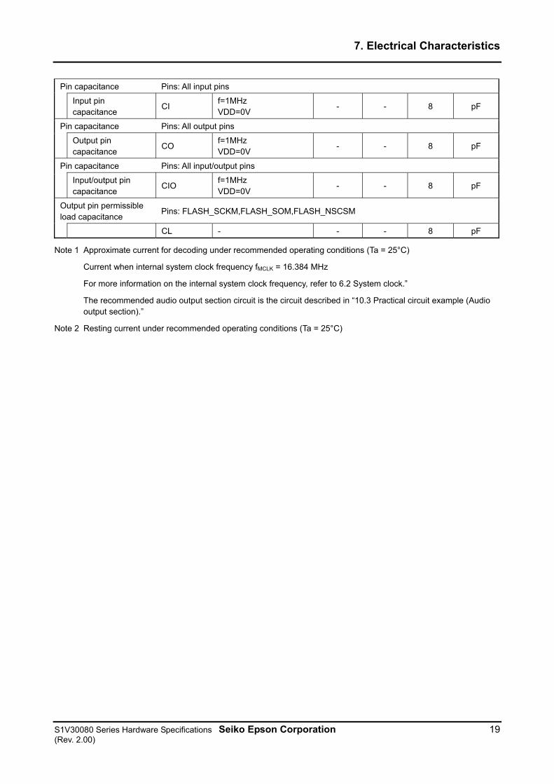
Note 1 Approximate current for decoding under recommended operating conditions (Ta = 25°C)
Current when internal system clock frequency fMCLK = 16.384 MHz
For more information on the internal system clock frequency, refer to 6.2 System clock.”
The recommended audio output section circuit is the circuit described in “10.3 Practical circuit example (Audio output section).”
Note 2 Resting current under recommended operating conditions (Ta = 25°C)
7. Electrical Characteristics
20 Seiko Epson Corporation S1V30080 Series Hardware Specifications (Rev. 2.00)
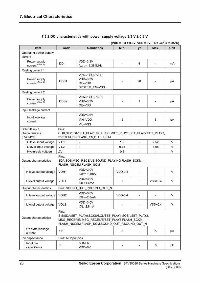
7.3.2 DC characteristics with power supply voltage 3.3 V ± 0.3 V
(VDD = 3.3 ± 0.3V, VSS = 0V, Ta = -40C to 85C)
Item Code Conditions Min. Typ. Max. Unit
Operating power supply current
Power supply current (Note 1)
IDD VDD=3.3V fMCLK=16.384MHz
- 4 - mA
Resting current 1
Power supply current (Note 2)
IDDS1
VIN=VDD or VSS VDD=3.3V CE=VDD SYSTEM_EN=VSS
- 20 - μA
Resting current 2
Power supply current (Note 2)
IDDS2 VIN=VDD or VSS VDD=3.3V CE=VSS
- 1 - μA
Input leakage current
VDD=3.6V
VIH=VDD -5 - 5 μA
Input leakage current
VIL=VSS
Schmitt input characteristics (LVCMOS)
Pins: CLKI,SIS/SDA/SET_PLAY0,SCKS/SCL/SET_PLAY1,SET_PLAY2,SET_PLAY3, SYSTEM_EN,FLASH_EN,FLASH_SIM
H level input voltage VIH2 - 1.2 - 2.52 V
L level input voltage VIL2 - 0.75 - 1.98 V
Hysteresis voltage ΔV - 0.3 - - V
Output characteristics Pins: SDA,SOS,MSG_RECEIVE,SOUND_PLAYING,FLASH_SCKM, FLASH_NSCSM,FLASH_SOM
H level output voltage VOH1 VDD=3.0V IOH=-1.4mA
VDD-0.4 - - V
L level output voltage VOL1 VDD=3.0V IOL=1.4mA
- - VSS+0.4 V
Output characteristics Pins: SOUND_OUT_P,SOUND_OUT_N
H level output voltage VOH2 VDD=3.0V IOH=-2.8mA
VDD-0.4 - - V
L level output voltage VOL2 VDD=3.0V IOL=2.8mA
- - VSS+0.4 V
Output characteristics
Pins: SIS/SDA/SET_PLAY0,SCKS/SCL/SET_PLAY1,SOS/-/SET_PLAY2, MSG_RECEIVE/ MSG_RECEIVE/SET_PLAY3,FLASH_SCKM, FLASH_NSCSM,FLASH_SOM,SOUND_OUT_P,SOUND_OUT_N
Off state leakage current
IOZ - -5 - 5 μA
Pin capacitance Pins: All input pins
Input pin capacitance
CI f=1MHz VDD=0V
- - 8 pF

7. Electrical Characteristics
S1V30080 Series Hardware Specifications Seiko Epson Corporation 21 (Rev. 2.00)
Pin capacitance Pins: All output pins
Output pin capacitance
CO f=1MHz VDD=0V
- - 8 pF
Pin capacitance Pins: All input/output pins
Input/output pin capacitance
CIO f=1MHz VDD=0V
- - 8 pF
Output pin permissible load capacitance
Pins: FLASH_SCKM,FLASH_SOM,FLASH_NSCSM
CL - - - 8 pF
Note 1 Approximate current for decoding under recommended operating conditions (Ta = 25°C)
Current when internal system clock frequency fMCLK = 16.384 MHz
For more information on the internal system clock frequency, refer to “6.2 System clock.”
The recommended audio output section circuit is the circuit described in “10.3 Practical circuit example (Audio output section).”
Note 2 Resting current under recommended operating conditions (Ta = 25°C)
7. Electrical Characteristics
22 Seiko Epson Corporation S1V30080 Series Hardware Specifications (Rev. 2.00)
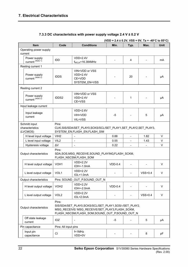
7.3.3 DC characteristics with power supply voltage 2.4 V ± 0.2 V
(VDD = 2.4 ± 0.2V, VSS = 0V, Ta = -40C to 85C)
Item Code Conditions Min. Typ. Max. Unit
Operating power supply current
Power supply current (Note 1)
IDD VDD=2.4V fMCLK=16.384MHz
- 4 - mA
Resting current 1
Power supply current (Note 2)
IDDS
VIN=VDD or VSS VDD=2.4V CE=VDD SYSTEM_EN=VSS
- 20 - μA
Resting current 2
Power supply current (Note 2)
IDDS2 VIN=VDD or VSS VDD=2.4V CE=VSS
- 1 - μA
Input leakage current
VDD=2.6V
VIH=VDD -5 - 5 μA Input leakage current
VIL=VSS
Schmitt input characteristics (LVCMOS)
Pins: CLKI,SIS/SDA/SET_PLAY0,SCKS/SCL/SET_PLAY1,SET_PLAY2,SET_PLAY3, SYSTEM_EN,FLASH_EN,FLASH_SIM
H level input voltage VIH2 - 0.88 - 1.82 V
L level input voltage VIL2 - 0.55 - 1.43 V
Hysteresis voltage ΔV - 0.22 - - V
Output characteristics Pins: SDA,SOS,MSG_RECEIVE,SOUND_PLAYING,FLASH_SCKM, FLASH_NSCSM,FLASH_SOM
H level output voltage VOH1 VDD=2.2V IOH=-1.0mA
VDD-0.4 - - V
L level output voltage VOL1 VDD=2.2V IOL=1.0mA
- - VSS+0.4 V
Output characteristics Pins: SOUND_OUT_P,SOUND_OUT_N
H level output voltage VOH2 VDD=2.2V IOH=-2.0mA
VDD-0.4 - - V
L level output voltage VOL2 VDD=2.2V IOL=2.0mA
- - VSS+0.4 V
Output characteristics
Pins: SIS/SDA/SET_PLAY0,SCKS/SCL/SET_PLAY1,SOS/-/SET_PLAY2, MSG_RECEIVE/ MSG_RECEIVE/SET_PLAY3,FLASH_SCKM, FLASH_NSCSM,FLASH_SOM,SOUND_OUT_P,SOUND_OUT_N
Off state leakage current
IOZ - -5 - 5 μA
Pin capacitance Pins: All input pins
Input pin capacitance
CI f=1MHz VDD=0V
- - 8 pF
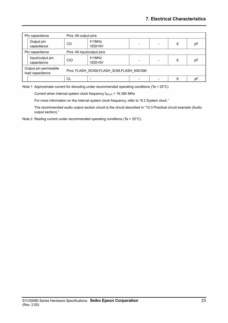
7. Electrical Characteristics
S1V30080 Series Hardware Specifications Seiko Epson Corporation 23 (Rev. 2.00)
Pin capacitance Pins: All output pins
Output pin capacitance
CO f=1MHz VDD=0V
- - 8 pF
Pin capacitance Pins: All input/output pins
Input/output pin capacitance
CIO f=1MHz VDD=0V
- - 8 pF
Output pin permissible load capacitance
Pins: FLASH_SCKM,FLASH_SOM,FLASH_NSCSM
CL - - - 8 pF
Note 1 Approximate current for decoding under recommended operating conditions (Ta = 25°C)
Current when internal system clock frequency fMCLK = 16.384 MHz
For more information on the internal system clock frequency, refer to “6.2 System clock.”
The recommended audio output section circuit is the circuit described in “10.3 Practical circuit example (Audio output section).”
Note 2 Resting current under recommended operating conditions (Ta = 25°C)
7. Electrical Characteristics
24 Seiko Epson Corporation S1V30080 Series Hardware Specifications (Rev. 2.00)
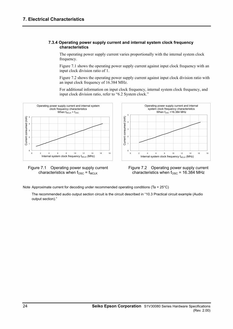
7.3.4 Operating power supply current and internal system clock frequency characteristics
The operating power supply current varies proportionally with the internal system clock frequency.
Figure 7.1 shows the operating power supply current against input clock frequency with an input clock division ratio of 1.
Figure 7.2 shows the operating power supply current against input clock division ratio with an input clock frequency of 16.384 MHz.
For additional information on input clock frequency, internal system clock frequency, and input clock division ratio, refer to “6.2 System clock.”
動作時電源電流 内部システムクロック周波数特性
fMCLK=fosc時
0
1
2
3
4
5
0 2 4 6 8 10 12 14 16 18
内部システムクロック周波数fMCLK(MHz)
消費電
流(m
A)
Figure 7.1 Operating power supply current characteristics when fOSC = fMCLK
動作時電源電流 内部システムクロック周波数特性fosc=16.384MHz時
0
1
2
3
4
5
0 2 4 6 8 10 12 14 16 18
内部システムクロック周波数fMCLK(MHz)
消費電流
(mA)
Figure 7.2 Operating power supply current characteristics when fOSC = 16.384 MHz
Note Approximate current for decoding under recommended operating conditions (Ta = 25°C)
The recommended audio output section circuit is the circuit described in “10.3 Practical circuit example (Audio output section).”
Operating power supply current and internal system clock frequency characteristics
When fMCLK = fOSC
Operating power supply current and internal system clock frequency characteristics
When fOSC =16.384 MHz
Cur
rent
con
sum
ed (
mA
)
Internal system clock frequency fMCLK (MHz)
Cur
rent
con
sum
ed (
mA
)
Internal system clock frequency fMCLK (MHz)
7. Electrical Characteristics
S1V30080 Series Hardware Specifications Seiko Epson Corporation 25 (Rev. 2.00)
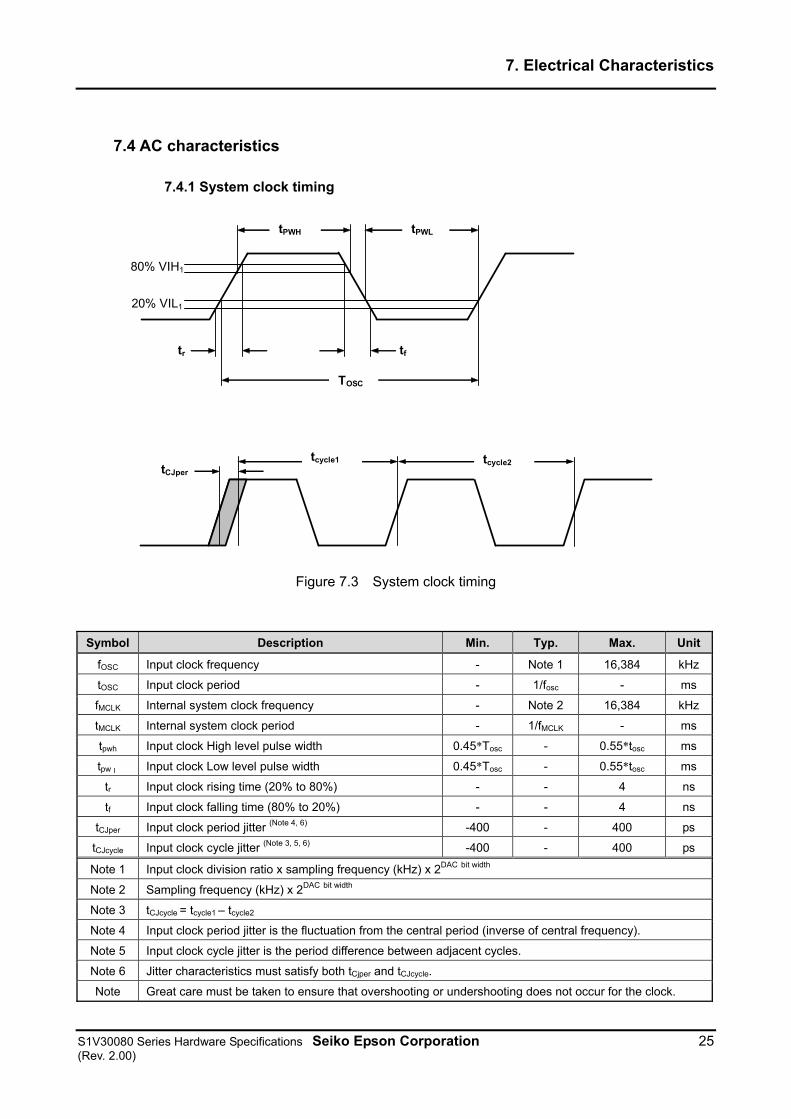
7.4 AC characteristics
7.4.1 System clock timing
80% VIH1
20% VIL1
tPWH tPWL
tr tf
TOSC
tCJper tcycle1 tcycle2
Figure 7.3 System clock timing
Symbol Description Min. Typ. Max. Unit
fOSC Input clock frequency - Note 1 16,384 kHz
tOSC Input clock period - 1/fosc - ms
fMCLK Internal system clock frequency - Note 2 16,384 kHz
tMCLK Internal system clock period - 1/fMCLK - ms
tpwh Input clock High level pulse width 0.45*Tosc - 0.55*tosc ms
tpwl Input clock Low level pulse width 0.45*Tosc - 0.55*tosc ms
tr Input clock rising time (20% to 80%) - - 4 ns
tf Input clock falling time (80% to 20%) - - 4 ns
tCJper Input clock period jitter (Note 4, 6) -400 - 400 ps
tCJcycle Input clock cycle jitter (Note 3, 5, 6) -400 - 400 ps
Note 1 Input clock division ratio x sampling frequency (kHz) x 2DAC bit width
Note 2 Sampling frequency (kHz) x 2DAC bit width
Note 3 tCJcycle = tcycle1 – tcycle2
Note 4 Input clock period jitter is the fluctuation from the central period (inverse of central frequency).
Note 5 Input clock cycle jitter is the period difference between adjacent cycles.
Note 6 Jitter characteristics must satisfy both tCjper and tCJcycle.
Note Great care must be taken to ensure that overshooting or undershooting does not occur for the clock.
7. Electrical Characteristics
26 Seiko Epson Corporation S1V30080 Series Hardware Specifications (Rev. 2.00)
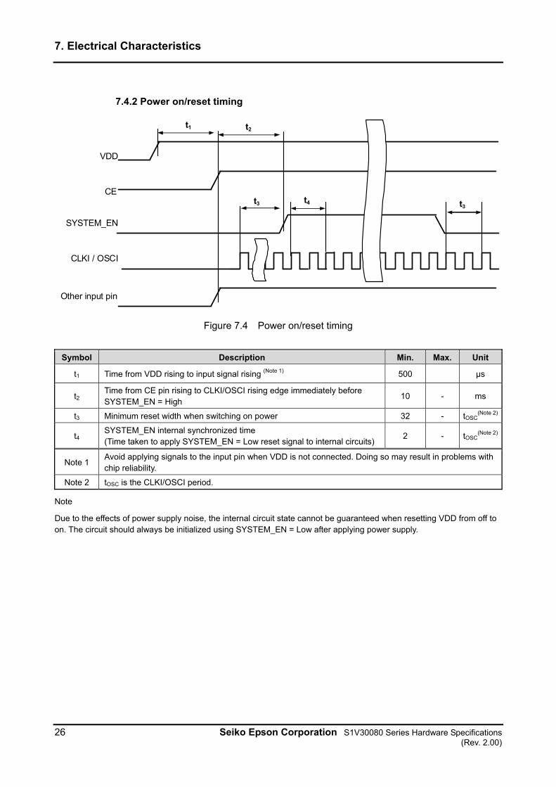
7.4.2 Power on/reset timing
VDD
SYSTEM_EN
CLKI / OSCI
t3
t2
t3t4
t1
CE
Other input pin
Figure 7.4 Power on/reset timing
Symbol Description Min. Max. Unit
t1 Time from VDD rising to input signal rising (Note 1) 500 μs
t2 Time from CE pin rising to CLKI/OSCI rising edge immediately before SYSTEM_EN = High
10 - ms
t3 Minimum reset width when switching on power 32 - tOSC(Note 2)
t4 SYSTEM_EN internal synchronized time (Time taken to apply SYSTEM_EN = Low reset signal to internal circuits)
2 - tOSC(Note 2)
Note 1 Avoid applying signals to the input pin when VDD is not connected. Doing so may result in problems with chip reliability.
Note 2 tOSC is the CLKI/OSCI period.
Note
Due to the effects of power supply noise, the internal circuit state cannot be guaranteed when resetting VDD from off to on. The circuit should always be initialized using SYSTEM_EN = Low after applying power supply.
7. Electrical Characteristics
S1V30080 Series Hardware Specifications Seiko Epson Corporation 27 (Rev. 2.00)
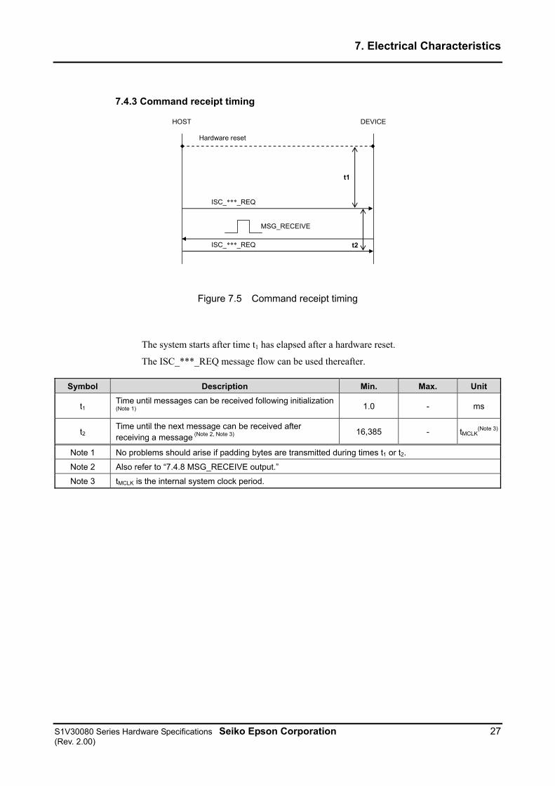
7.4.3 Command receipt timing
ISC_***_REQ
HOST DEVICE
t1
Hardware reset
MSG_RECEIVE
t2ISC_***_REQ
Figure 7.5 Command receipt timing
The system starts after time t1 has elapsed after a hardware reset.
The ISC_***_REQ message flow can be used thereafter.
Symbol Description Min. Max. Unit
t1 Time until messages can be received following initialization (Note 1)
1.0 - ms
t2 Time until the next message can be received after receiving a message (Note 2, Note 3)
16,385 - tMCLK(Note 3)
Note 1 No problems should arise if padding bytes are transmitted during times t1 or t2.
Note 2 Also refer to “7.4.8 MSG_RECEIVE output.”
Note 3 tMCLK is the internal system clock period.
7. Electrical Characteristics
28 Seiko Epson Corporation S1V30080 Series Hardware Specifications (Rev. 2.00)
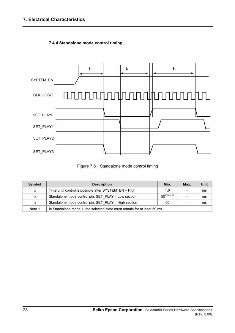
7.4.4 Standalone mode control timing
SET_PLAY0
SYSTEM_EN
CLKI / OSCI
t1 t2 t3
SET_PLAY1
SET_PLAY3
SET_PLAY2
Figure 7.6 Standalone mode control timing
Symbol Description Min. Max. Unit
t1 Time until control is possible after SYSTEM_EN = High 1.0 - ms
t2 Standalone mode control pin: SET_PLAY = Low section 50(Note 1) - ms
t3 Standalone mode control pin: SET_PLAY = High section 50 - ms
Note 1 In Standalone mode 1, the selected state must remain for at least 50 ms.
7. Electrical Characteristics
S1V30080 Series Hardware Specifications Seiko Epson Corporation 29 (Rev. 2.00)
7.4.5 Initialization timing from external serial flash memory
SYSTEM_EN
CLKI / OSCI
t1
FLASH_SCKM
t2
Figure 7.7 Initialization timing from external serial flash memory
Symbol Description Min. Max. Unit
t1 Initialization start time after SYSTEM_EN = High 3.5 - TOSC(Note 1)
t2 Initialization end time after SYSTEM_EN = High 1 - ms
Note 1 TOSC is the CLKI/OSCI period.
Note SYSTEM_EN should be controlled based on the start time required for external serial flash memory.
7. Electrical Characteristics
30 Seiko Epson Corporation S1V30080 Series Hardware Specifications (Rev. 2.00)
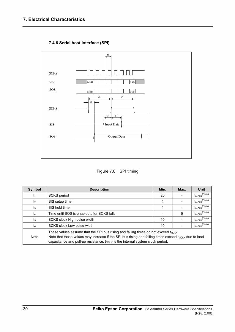
7.4.6 Serial host interface (SPI)
SCKS
SIS
t2 t3
t4
SOS
MSB LSB
MSB
SIS
SOS
t1
SCKS
LSB
Input Data
Output Data
t6 t5
Figure 7.8 SPI timing
Symbol Description Min. Max. Unit
t1 SCKS period 20 - tMCLK(Note)
t2 SIS setup time 4 - tMCLK(Note)
t3 SIS hold time 4 - tMCLK(Note)
t4 Time until SOS is enabled after SCKS falls - 5 tMCLK(Note)
t5 SCKS clock High pulse width 10 - tMCLK(Note)
t6 SCKS clock Low pulse width 10 - tMCLK(Note)
Note These values assume that the SPI bus rising and falling times do not exceed tMCLK. Note that these values may increase if the SPI bus rising and falling times exceed tMCLK due to load capacitance and pull-up resistance. tMCLK is the internal system clock period.
7. Electrical Characteristics
S1V30080 Series Hardware Specifications Seiko Epson Corporation 31 (Rev. 2.00)
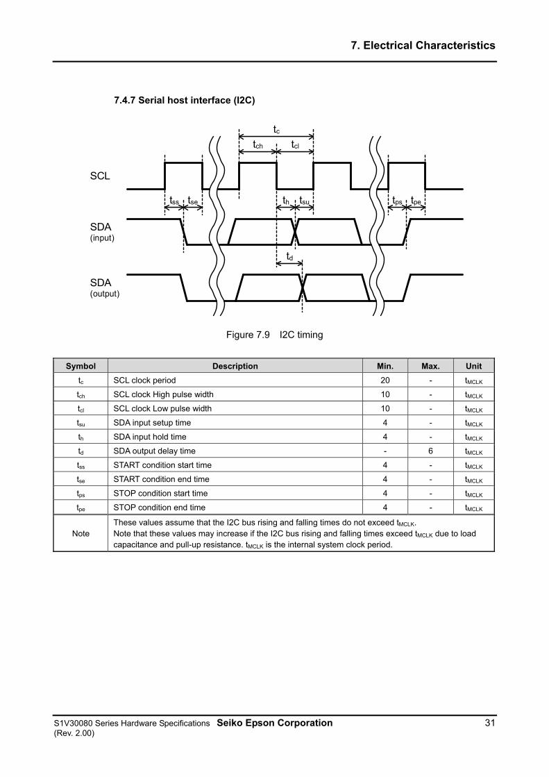
7.4.7 Serial host interface (I2C)
tctch tcl
th tsutss tse tps tpe
td
SCL
SDA(input)
SDA(output)
Figure 7.9 I2C timing
Symbol Description Min. Max. Unit
tc SCL clock period 20 - tMCLK
tch SCL clock High pulse width 10 - tMCLK
tcl SCL clock Low pulse width 10 - tMCLK
tsu SDA input setup time 4 - tMCLK
th SDA input hold time 4 - tMCLK
td SDA output delay time - 6 tMCLK
tss START condition start time 4 - tMCLK
tse START condition end time 4 - tMCLK
tps STOP condition start time 4 - tMCLK
tpe STOP condition end time 4 - tMCLK
Note These values assume that the I2C bus rising and falling times do not exceed tMCLK. Note that these values may increase if the I2C bus rising and falling times exceed tMCLK due to load capacitance and pull-up resistance. tMCLK is the internal system clock period.
7. Electrical Characteristics
32 Seiko Epson Corporation S1V30080 Series Hardware Specifications (Rev. 2.00)
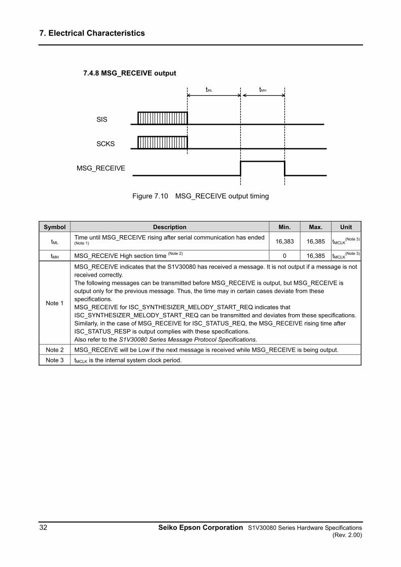
7.4.8 MSG_RECEIVE output
SIS
SCKS
MSG_RECEIVE
tML tMH
Figure 7.10 MSG_RECEIVE output timing
Symbol Description Min. Max. Unit
tML Time until MSG_RECEIVE rising after serial communication has ended (Note 1)
16,383 16,385 tMCLK(Note 3)
tMH MSG_RECEIVE High section time (Note 2) 0 16,385 tMCLK(Note 3)
Note 1
MSG_RECEIVE indicates that the S1V30080 has received a message. It is not output if a message is not received correctly. The following messages can be transmitted before MSG_RECEIVE is output, but MSG_RECEIVE is output only for the previous message. Thus, the time may in certain cases deviate from these specifications. MSG_RECEIVE for ISC_SYNTHESIZER_MELODY_START_REQ indicates that ISC_SYNTHESIZER_MELODY_START_REQ can be transmitted and deviates from these specifications.Similarly, in the case of MSG_RECEIVE for ISC_STATUS_REQ, the MSG_RECEIVE rising time after ISC_STATUS_RESP is output complies with these specifications. Also refer to the S1V30080 Series Message Protocol Specifications.
Note 2 MSG_RECEIVE will be Low if the next message is received while MSG_RECEIVE is being output.
Note 3 tMCLK is the internal system clock period.
7. Electrical Characteristics
S1V30080 Series Hardware Specifications Seiko Epson Corporation 33 (Rev. 2.00)
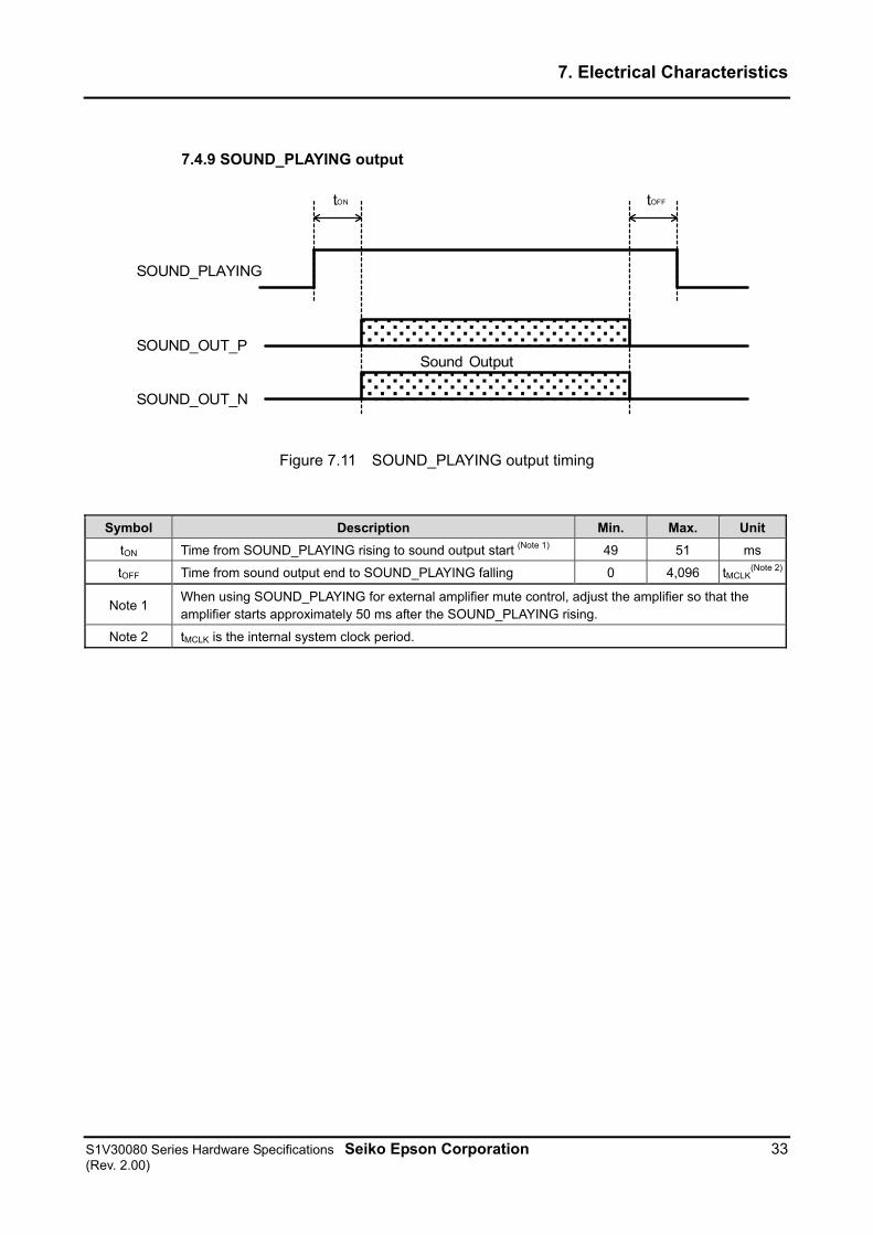
7.4.9 SOUND_PLAYING output
Figure 7.11 SOUND_PLAYING output timing
Symbol Description Min. Max. Unit
tON Time from SOUND_PLAYING rising to sound output start (Note 1) 49 51 ms
tOFF Time from sound output end to SOUND_PLAYING falling 0 4,096 tMCLK(Note 2)
Note 1 When using SOUND_PLAYING for external amplifier mute control, adjust the amplifier so that the amplifier starts approximately 50 ms after the SOUND_PLAYING rising.
Note 2 tMCLK is the internal system clock period.
tON
SOUND_PLAYING
SOUND_OUT_P
SOUND_OUT_N
tOFF
Sound Output
7. Electrical Characteristics
34 Seiko Epson Corporation S1V30080 Series Hardware Specifications (Rev. 2.00)
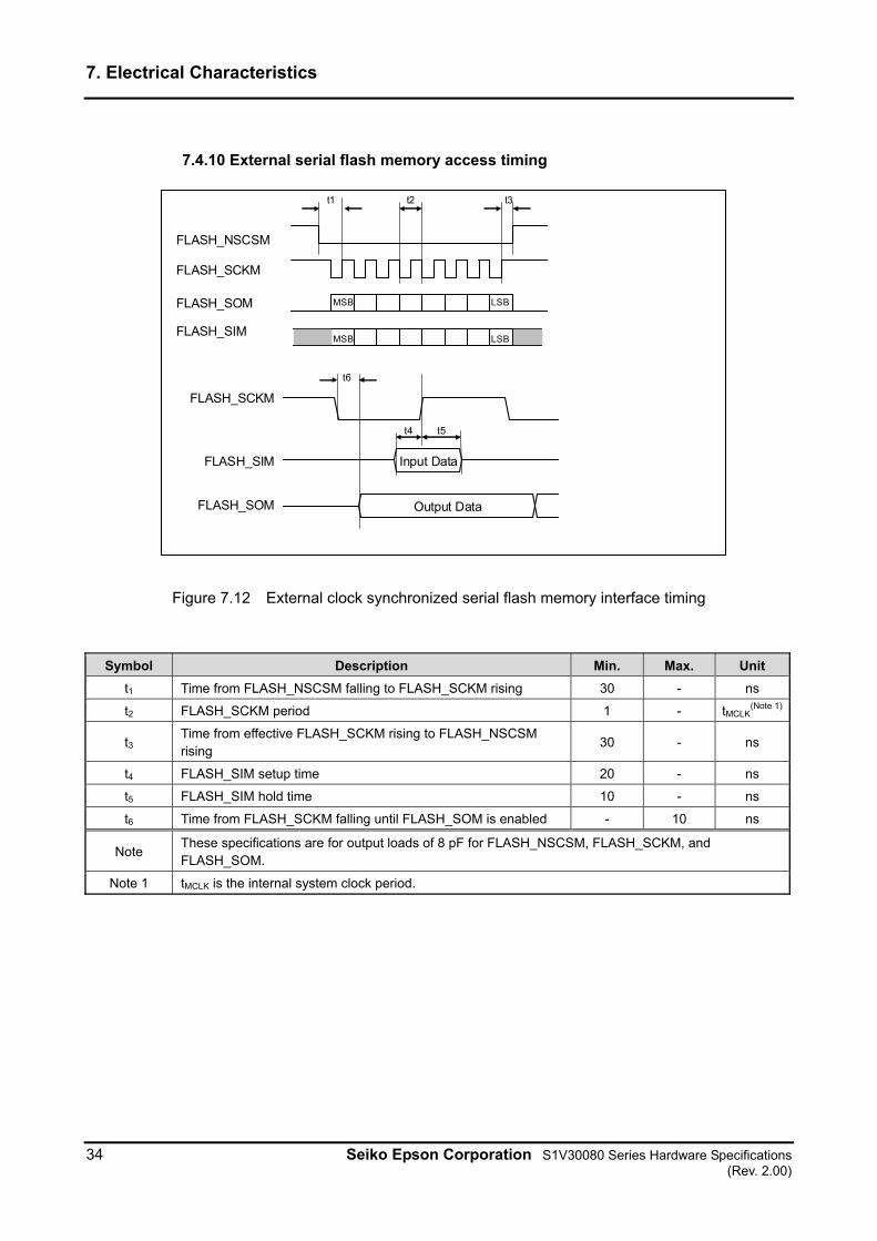
7.4.10 External serial flash memory access timing
FLASH_SCKM
FLASH_SIM
t4 t5
t6
FLASH_SOM
MSB LSB FLASH_SOM
FLASH_SIM
FLASH_NSCSM
t1 t3t2
FLASH_SCKM
LSB
Input Data
Output Data
MSB
Figure 7.12 External clock synchronized serial flash memory interface timing
Symbol Description Min. Max. Unit
t1 Time from FLASH_NSCSM falling to FLASH_SCKM rising 30 - ns
t2 FLASH_SCKM period 1 - tMCLK(Note 1)
t3 Time from effective FLASH_SCKM rising to FLASH_NSCSM rising
30 - ns
t4 FLASH_SIM setup time 20 - ns
t5 FLASH_SIM hold time 10 - ns
t6 Time from FLASH_SCKM falling until FLASH_SOM is enabled - 10 ns
Note These specifications are for output loads of 8 pF for FLASH_NSCSM, FLASH_SCKM, and FLASH_SOM.
Note 1 tMCLK is the internal system clock period.
7. Electrical Characteristics
S1V30080 Series Hardware Specifications Seiko Epson Corporation 35 (Rev. 2.00)
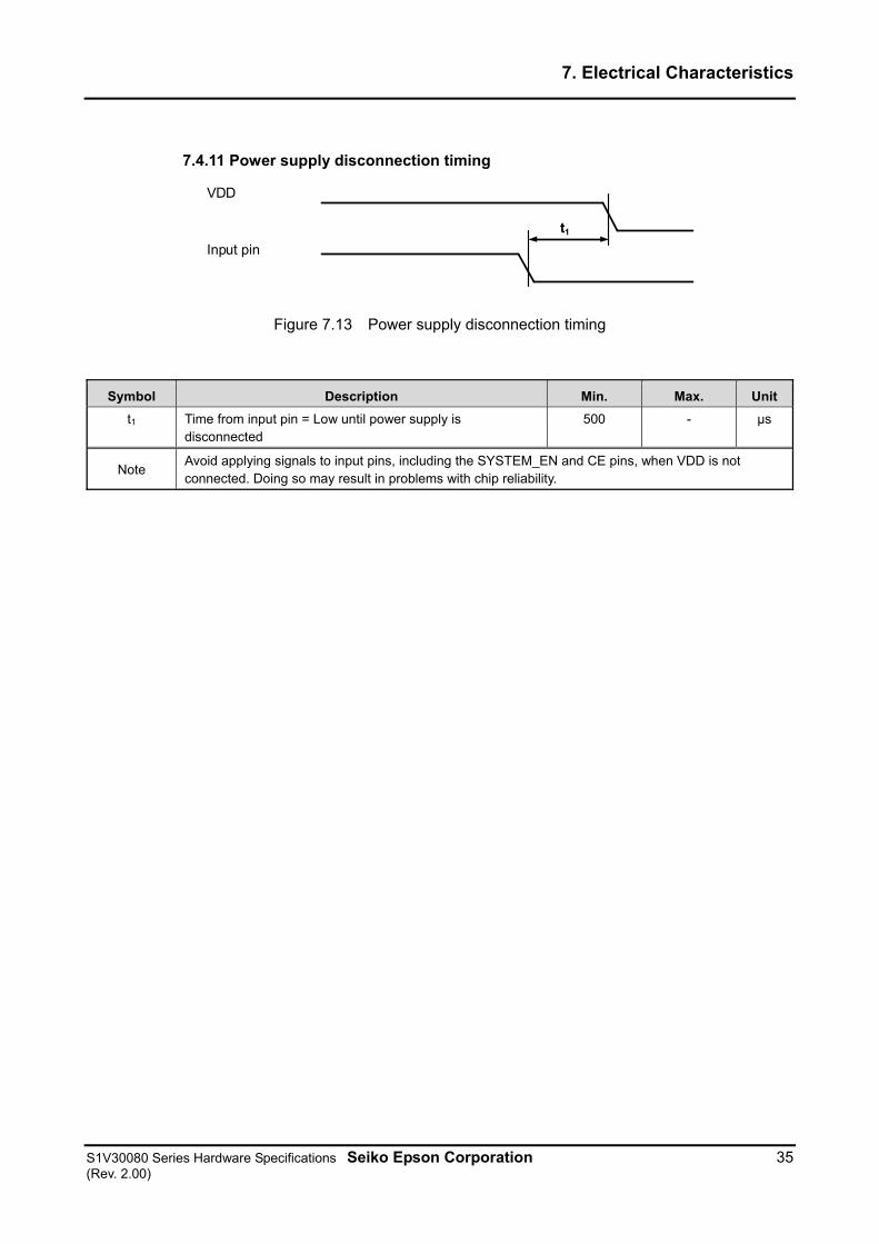
7.4.11 Power supply disconnection timing
VDD
Input pin
t1
Figure 7.13 Power supply disconnection timing
Symbol Description Min. Max. Unit
t1 Time from input pin = Low until power supply is disconnected
500 - μs
Note Avoid applying signals to input pins, including the SYSTEM_EN and CE pins, when VDD is not connected. Doing so may result in problems with chip reliability.
7. Electrical Characteristics
36 Seiko Epson Corporation S1V30080 Series Hardware Specifications (Rev. 2.00)
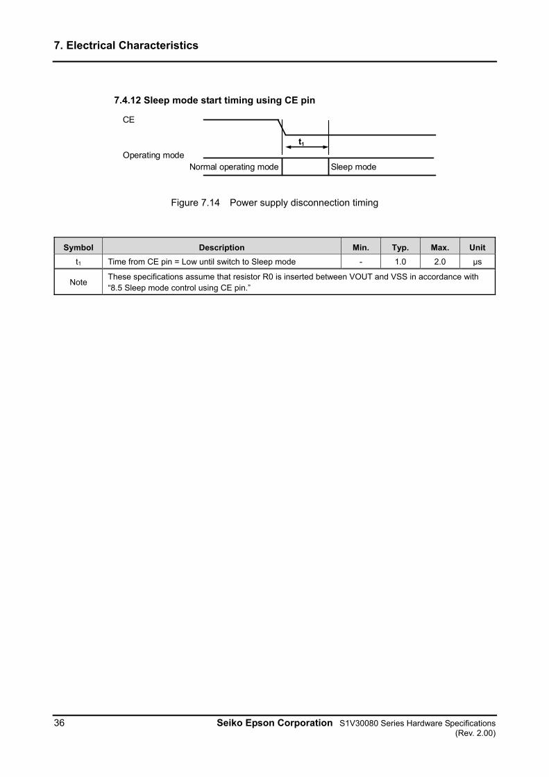
7.4.12 Sleep mode start timing using CE pin
CE
Operating mode
t1
Normal operating mode
Sleep mode
Figure 7.14 Power supply disconnection timing
Symbol Description Min. Typ. Max. Unit
t1 Time from CE pin = Low until switch to Sleep mode - 1.0 2.0 μs
Note These specifications assume that resistor R0 is inserted between VOUT and VSS in accordance with “8.5 Sleep mode control using CE pin.”
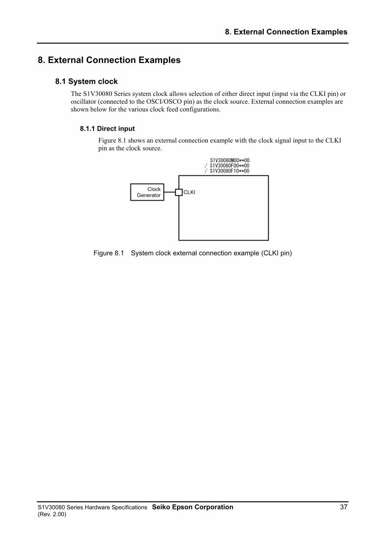
8. External Connection Examples
S1V30080 Series Hardware Specifications Seiko Epson Corporation 37 (Rev. 2.00)
8. External Connection Examples
8.1 System clock
The S1V30080 Series system clock allows selection of either direct input (input via the CLKI pin) or oscillator (connected to the OSCI/OSCO pin) as the clock source. External connection examples are shown below for the various clock feed configurations.
8.1.1 Direct input
Figure 8.1 shows an external connection example with the clock signal input to the CLKI pin as the clock source.
S1V30080M00**00/ S1V30080F00**00/ S1V30080F10**00
CLKIClock
Generator
Figure 8.1 System clock external connection example (CLKI pin)
8. External Connection Examples
38 Seiko Epson Corporation S1V30080 Series Hardware Specifications (Rev. 2.00)
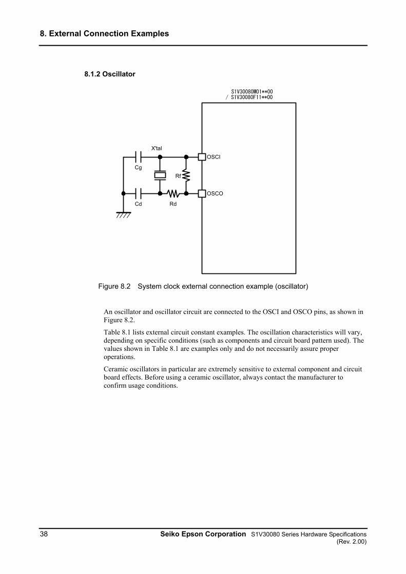
8.1.2 Oscillator
Rf
RdCd
Cg
X'tal
OSCO
OSCI
S1V30080M01**00/ S1V30080F11**00
Figure 8.2 System clock external connection example (oscillator)
An oscillator and oscillator circuit are connected to the OSCI and OSCO pins, as shown in Figure 8.2.
Table 8.1 lists external circuit constant examples. The oscillation characteristics will vary, depending on specific conditions (such as components and circuit board pattern used). The values shown in Table 8.1 are examples only and do not necessarily assure proper operations.
Ceramic oscillators in particular are extremely sensitive to external component and circuit board effects. Before using a ceramic oscillator, always contact the manufacturer to confirm usage conditions.
8. External Connection Examples
S1V30080 Series Hardware Specifications Seiko Epson Corporation 39 (Rev. 2.00)
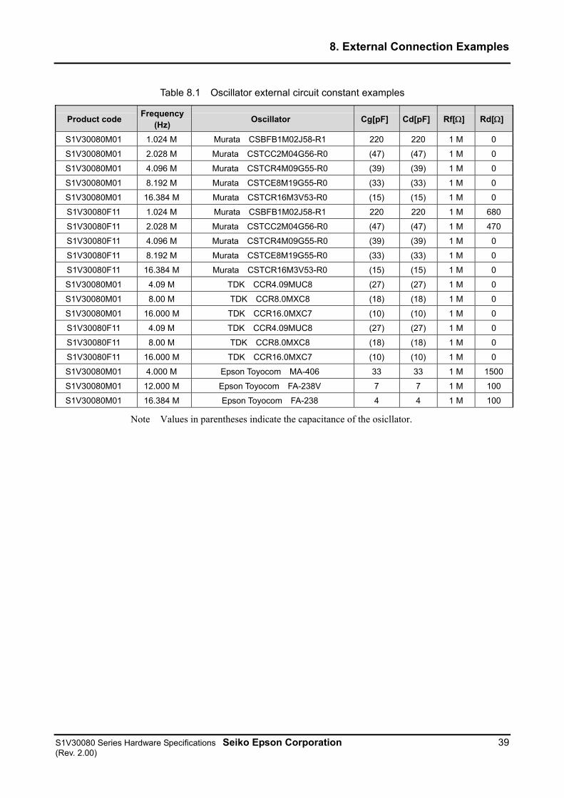
Table 8.1 Oscillator external circuit constant examples
Product code Frequency
(Hz) Oscillator Cg[pF] Cd[pF] Rf[] Rd[]
S1V30080M01 1.024 M Murata CSBFB1M02J58-R1 220 220 1 M 0
S1V30080M01 2.028 M Murata CSTCC2M04G56-R0 (47) (47) 1 M 0
S1V30080M01 4.096 M Murata CSTCR4M09G55-R0 (39) (39) 1 M 0
S1V30080M01 8.192 M Murata CSTCE8M19G55-R0 (33) (33) 1 M 0
S1V30080M01 16.384 M Murata CSTCR16M3V53-R0 (15) (15) 1 M 0
S1V30080F11 1.024 M Murata CSBFB1M02J58-R1 220 220 1 M 680
S1V30080F11 2.028 M Murata CSTCC2M04G56-R0 (47) (47) 1 M 470
S1V30080F11 4.096 M Murata CSTCR4M09G55-R0 (39) (39) 1 M 0
S1V30080F11 8.192 M Murata CSTCE8M19G55-R0 (33) (33) 1 M 0
S1V30080F11 16.384 M Murata CSTCR16M3V53-R0 (15) (15) 1 M 0
S1V30080M01 4.09 M TDK CCR4.09MUC8 (27) (27) 1 M 0
S1V30080M01 8.00 M TDK CCR8.0MXC8 (18) (18) 1 M 0
S1V30080M01 16.000 M TDK CCR16.0MXC7 (10) (10) 1 M 0
S1V30080F11 4.09 M TDK CCR4.09MUC8 (27) (27) 1 M 0
S1V30080F11 8.00 M TDK CCR8.0MXC8 (18) (18) 1 M 0
S1V30080F11 16.000 M TDK CCR16.0MXC7 (10) (10) 1 M 0
S1V30080M01 4.000 M Epson Toyocom MA-406 33 33 1 M 1500
S1V30080M01 12.000 M Epson Toyocom FA-238V 7 7 1 M 100
S1V30080M01 16.384 M Epson Toyocom FA-238 4 4 1 M 100
Note Values in parentheses indicate the capacitance of the osicllator.
8. External Connection Examples
40 Seiko Epson Corporation S1V30080 Series Hardware Specifications (Rev. 2.00)
8.2 Serial host interface
8.2.1 SPI
HOST
S1V30080
Serial Clock Out
Serial Data Out
Serial Data In
External Interrupt Port
I/O Port
SCKS/SCL/SET_PLAY1
SIS/SDA/SET_PLAY0
SOS/-/SET_PLAY2
MSG_RECEIVE/SET_PLAY3
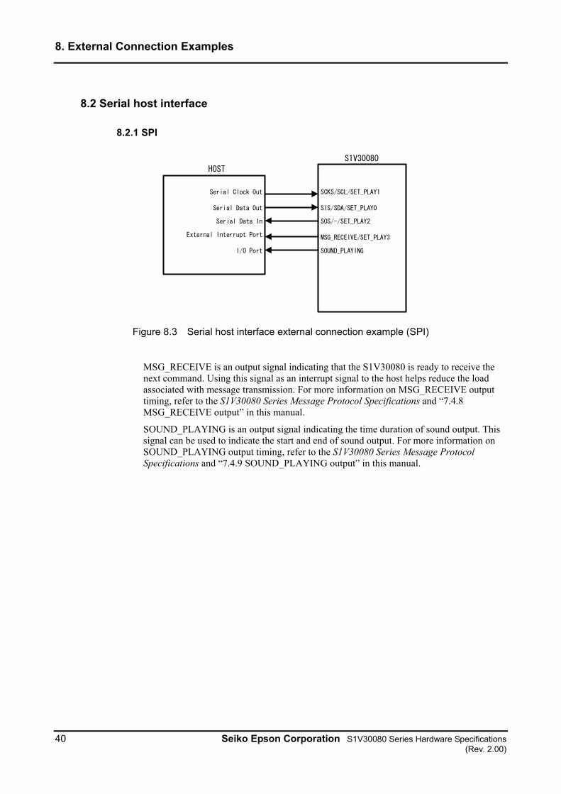
SOUND_PLAYING
Figure 8.3 Serial host interface external connection example (SPI)
MSG_RECEIVE is an output signal indicating that the S1V30080 is ready to receive the next command. Using this signal as an interrupt signal to the host helps reduce the load associated with message transmission. For more information on MSG_RECEIVE output timing, refer to the S1V30080 Series Message Protocol Specifications and “7.4.8 MSG_RECEIVE output” in this manual.
SOUND_PLAYING is an output signal indicating the time duration of sound output. This signal can be used to indicate the start and end of sound output. For more information on SOUND_PLAYING output timing, refer to the S1V30080 Series Message Protocol Specifications and “7.4.9 SOUND_PLAYING output” in this manual.
8. External Connection Examples
S1V30080 Series Hardware Specifications Seiko Epson Corporation 41 (Rev. 2.00)
8.2.2 I2C
HOST
S1V30080
SCL
SDA
External Interrupt Port
I/O Port
SCKS/SCL/SET_PLAY1
SIS/SDA/SET_PLAY0
SOS/-/SET_PLAY2
MSG_RECEIVE/SET_PLAY3
SOUND_PLAYING
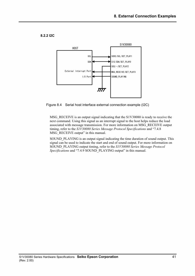
Figure 8.4 Serial host interface external connection example (I2C)
MSG_RECEIVE is an output signal indicating that the S1V30080 is ready to receive the next command. Using this signal as an interrupt signal to the host helps reduce the load associated with message transmission. For more information on MSG_RECEIVE output timing, refer to the S1V30080 Series Message Protocol Specifications and “7.4.8 MSG_RECEIVE output” in this manual.
SOUND_PLAYING is an output signal indicating the time duration of sound output. This signal can be used to indicate the start and end of sound output. For more information on SOUND_PLAYING output timing, refer to the S1V30080 Series Message Protocol Specifications and “7.4.9 SOUND_PLAYING output” in this manual.
8. External Connection Examples
42 Seiko Epson Corporation S1V30080 Series Hardware Specifications (Rev. 2.00)
8.3 Standalone connection
S1V30080
SCKS/SCL/SET_PLAY1
SIS/SDA/SET_PLAY0
SOS/-/SET_PLAY2
MSG_RECEIVE/SET_PLAY3
Switch
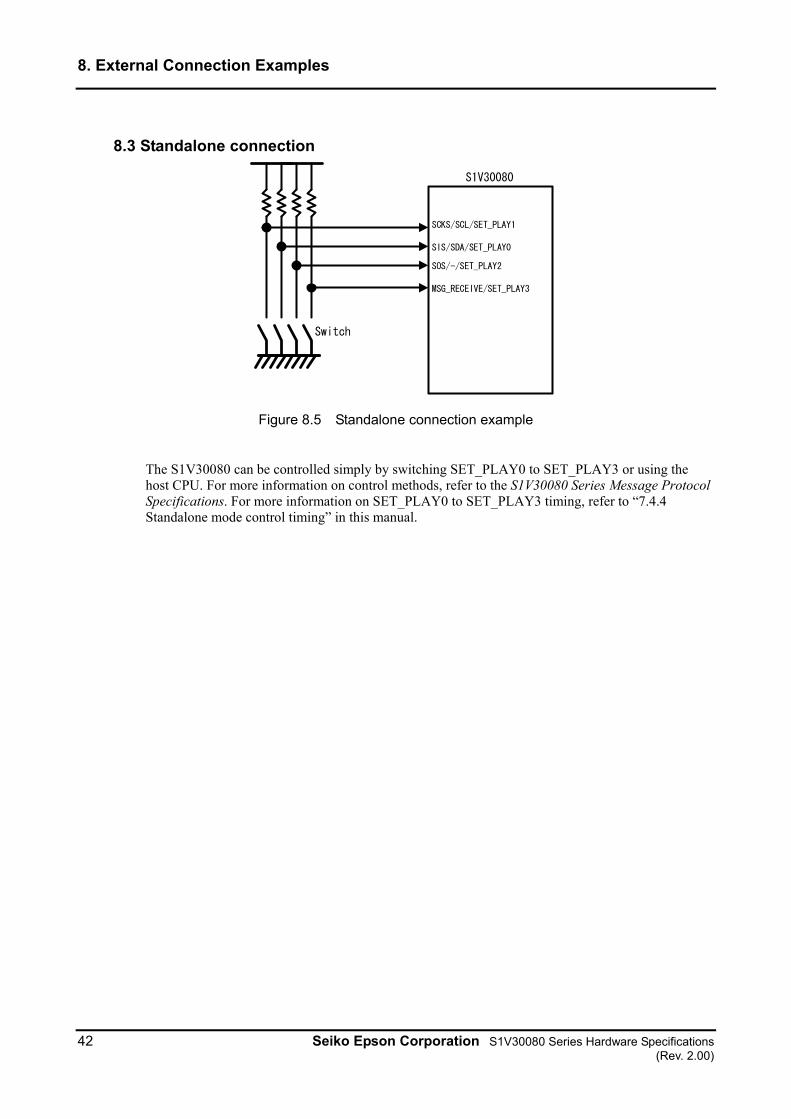
Figure 8.5 Standalone connection example
The S1V30080 can be controlled simply by switching SET_PLAY0 to SET_PLAY3 or using the host CPU. For more information on control methods, refer to the S1V30080 Series Message Protocol Specifications. For more information on SET_PLAY0 to SET_PLAY3 timing, refer to “7.4.4 Standalone mode control timing” in this manual.
8. External Connection Examples
S1V30080 Series Hardware Specifications Seiko Epson Corporation 43 (Rev. 2.00)
8.4 External serial flash memory interface
Clock Synchronous SerialI/F Flash Memory
S1V30080
FLASH_SCKM
FLASH_SIM
FLASH_SOM
FLASH_NSCSM
SCK
#CS
SI
SO
FLASH_EN
VDD
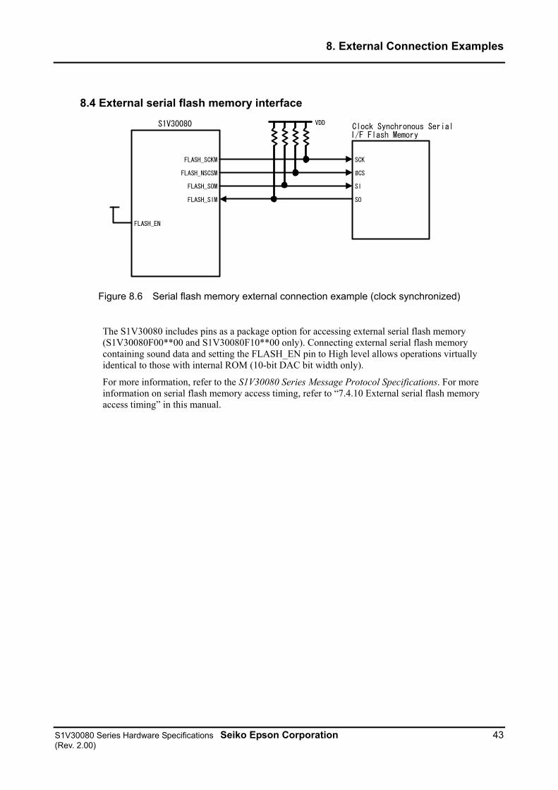
Figure 8.6 Serial flash memory external connection example (clock synchronized)
The S1V30080 includes pins as a package option for accessing external serial flash memory (S1V30080F00**00 and S1V30080F10**00 only). Connecting external serial flash memory containing sound data and setting the FLASH_EN pin to High level allows operations virtually identical to those with internal ROM (10-bit DAC bit width only).
For more information, refer to the S1V30080 Series Message Protocol Specifications. For more information on serial flash memory access timing, refer to “7.4.10 External serial flash memory access timing” in this manual.
8. External Connection Examples
44 Seiko Epson Corporation S1V30080 Series Hardware Specifications (Rev. 2.00)
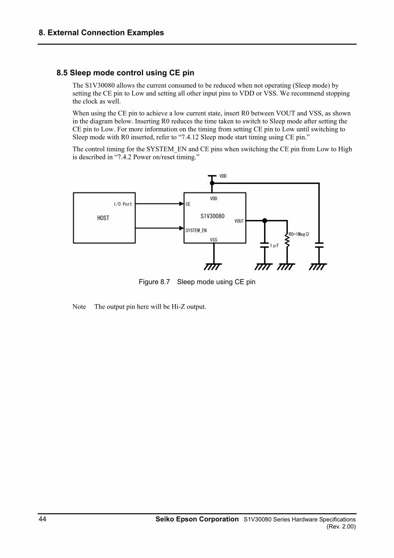
8.5 Sleep mode control using CE pin
The S1V30080 allows the current consumed to be reduced when not operating (Sleep mode) by setting the CE pin to Low and setting all other input pins to VDD or VSS. We recommend stopping the clock as well.
When using the CE pin to achieve a low current state, insert R0 between VOUT and VSS, as shown in the diagram below. Inserting R0 reduces the time taken to switch to Sleep mode after setting the CE pin to Low. For more information on the timing from setting CE pin to Low until switching to Sleep mode with R0 inserted, refer to “7.4.12 Sleep mode start timing using CE pin.”
The control timing for the SYSTEM_EN and CE pins when switching the CE pin from Low to High is described in “7.4.2 Power on/reset timing.”
S1V30080
VDD
HOST
CE
SYSTEM_EN
VOUT
VSS
I/O Port
1μF
R0=1MegΩ
VDD
Figure 8.7 Sleep mode using CE pin
Note The output pin here will be Hi-Z output.
9. Package Information
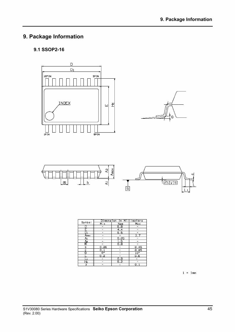
S1V30080 Series Hardware Specifications Seiko Epson Corporation 45 (Rev. 2.00)
9. Package Information
9.1 SSOP2-16
9. Package Information
46 Seiko Epson Corporation S1V30080 Series Hardware Specifications (Rev. 2.00)
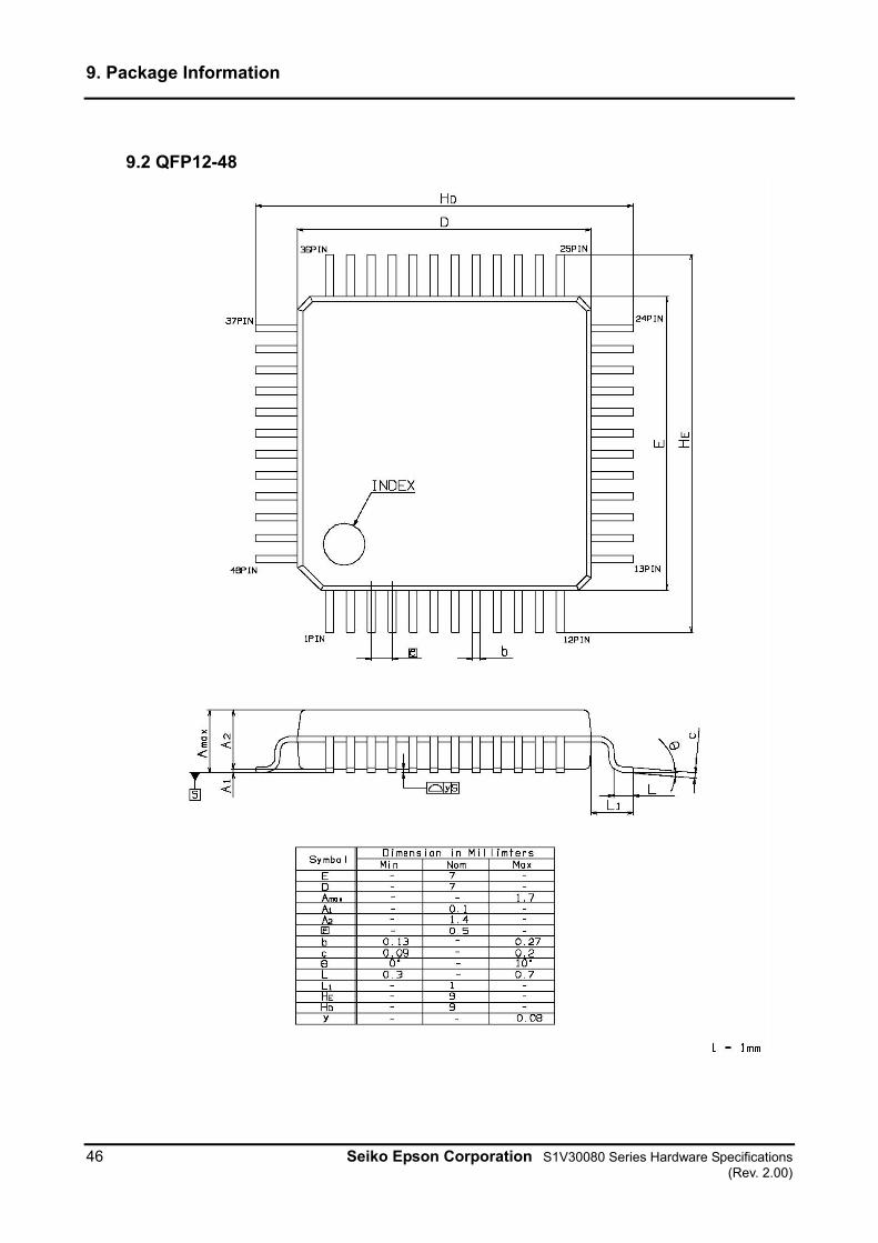
9.2 QFP12-48
9. Package Information
S1V30080 Series Hardware Specifications Seiko Epson Corporation 47 (Rev. 2.00)
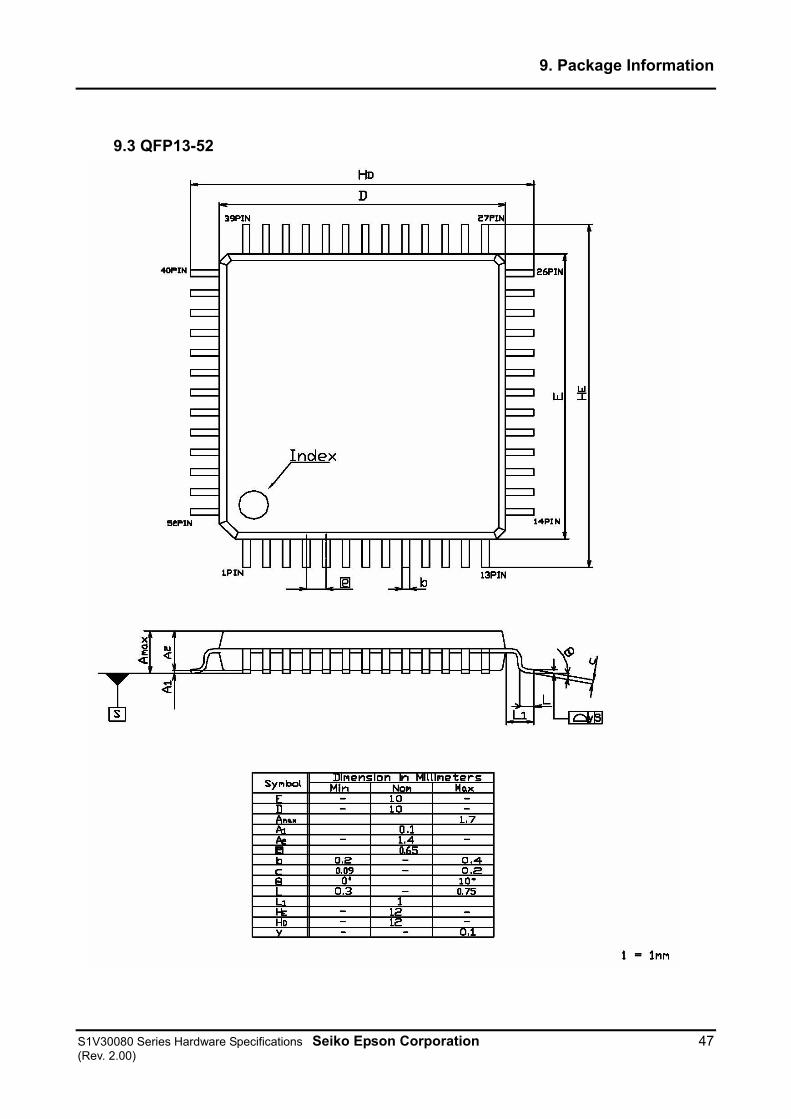
9.3 QFP13-52
10. Reference Material
48 Seiko Epson Corporation S1V30080 Series Hardware Specifications (Rev. 2.00)
10. Reference Material
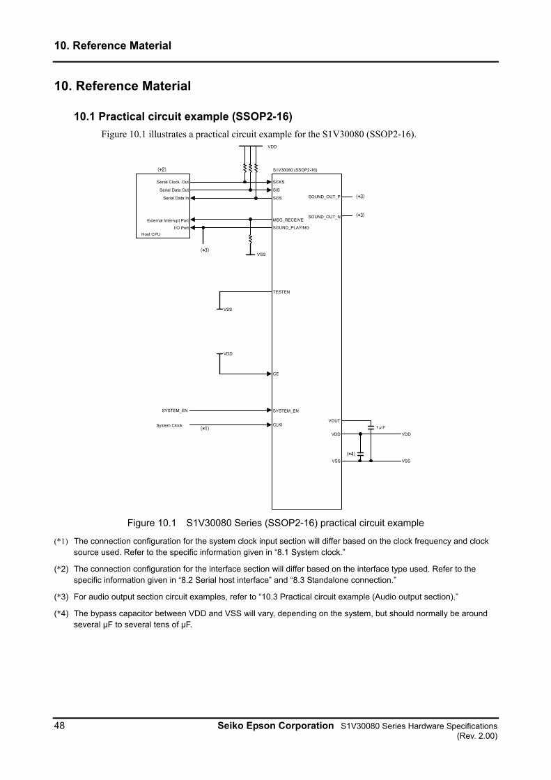
10.1 Practical circuit example (SSOP2-16)
Figure 10.1 illustrates a practical circuit example for the S1V30080 (SSOP2-16).
CLKI
SCKS
SIS
SOS
TESTEN
MSG_RECEIVE
SYSTEM_EN
SOUND_PLAYING
VOUT
VDD
VSS
SOUND_OUT_P
S1V30080 (SSOP2-16)
CE
Serial Clock Out
Serial Data Out
Serial Data In
External Interrupt Port
I/O Port
VSS
SYSTEM_EN
1μF
VSS
VDD
VDD
System Clock
SOUND_OUT_N
VSS
Host CPU
(*2)
(*3)
(*3)
(*3)
VDD
(*1)
(*4)
Figure 10.1 S1V30080 Series (SSOP2-16) practical circuit example
(*1) The connection configuration for the system clock input section will differ based on the clock frequency and clock source used. Refer to the specific information given in “8.1 System clock.”
(*2) The connection configuration for the interface section will differ based on the interface type used. Refer to the specific information given in “8.2 Serial host interface” and “8.3 Standalone connection.”
(*3) For audio output section circuit examples, refer to “10.3 Practical circuit example (Audio output section).”
(*4) The bypass capacitor between VDD and VSS will vary, depending on the system, but should normally be around several µF to several tens of µF.
10. Reference Material
S1V30080 Series Hardware Specifications Seiko Epson Corporation 49 (Rev. 2.00)
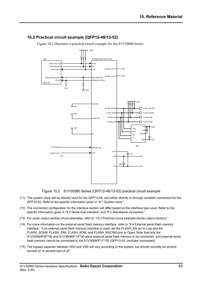
10.2 Practical circuit example (QFP12-48/13-52)
Figure 10.2 illustrates a practical circuit example for the S1V30080 Series.
CLKI
SCKS
SIS
SOS
TESTEN
MSG_RECEIVE
SYSTEM_EN
SOUND_PLAYING
VOUT
VDD
VSS
SOUND_OUT_P
S1V30080 (QFP12-48/13-52)
CE
Serial Clock Out
Serial Data Out
Serial Data In
External Interrupt Port
I/O Port
VSS
SYSTEM_EN
1μF
FLASH_EN
VSS
VDD
W#
GND
Vcc
HOLD#
VSS
FLASH_NSCSM
FLASH_SCKM
FLASH_SIM
FLASH_SOM
FLASH_NSCSM
FLASH_SCKM
FLASH_SIM
FLASH_SOM
CS#
SCK
SO
SI
VDD
System Clock
SOUND_OUT_N
VDD
VDD
VDD
VSS
Host CPU
(*2)
(*3)
(*4)
(*1)
(*3)
(*3)
VDD
(*5)
Figure 10.2 S1V30080 Series (QFP12-48/13-52) practical circuit example
(*1) The system clock will be directly input for the QFP12-48, and either directly or through oscillator connection for the QFP13-52. Refer to the specific information given in “8.1 System clock.”
(*2) The connection configuration for the interface section will differ based on the interface type used. Refer to the specific information given in “8.2 Serial host interface” and “8.3 Standalone connection.”
(*3) For audio output section circuit examples, refer to “10.3 Practical circuit example (Audio output section).”
(*4) For more information on the external serial flash memory interface, refer to “8.4 External serial flash memory interface.” If no external serial flash memory interface is used, set the FLASH_EN pin to Low and the FLASH_SCKM, FLASH_SIM, FLASH_SOM, and FLASH_NSCSM pins to Open. Note that only the S1V30080F00**00 and S1V30080F10**00 allow external serial flash memory to be connected, and external serial flash memory cannot be connected to the S1V30080F11**00 (QFP13-52, oscillator connected).
(*5) The bypass capacitor between VDD and VSS will vary according to the system, but should normally be around several µF to several tens of µF.
10. Reference Material
50 Seiko Epson Corporation S1V30080 Series Hardware Specifications (Rev. 2.00)
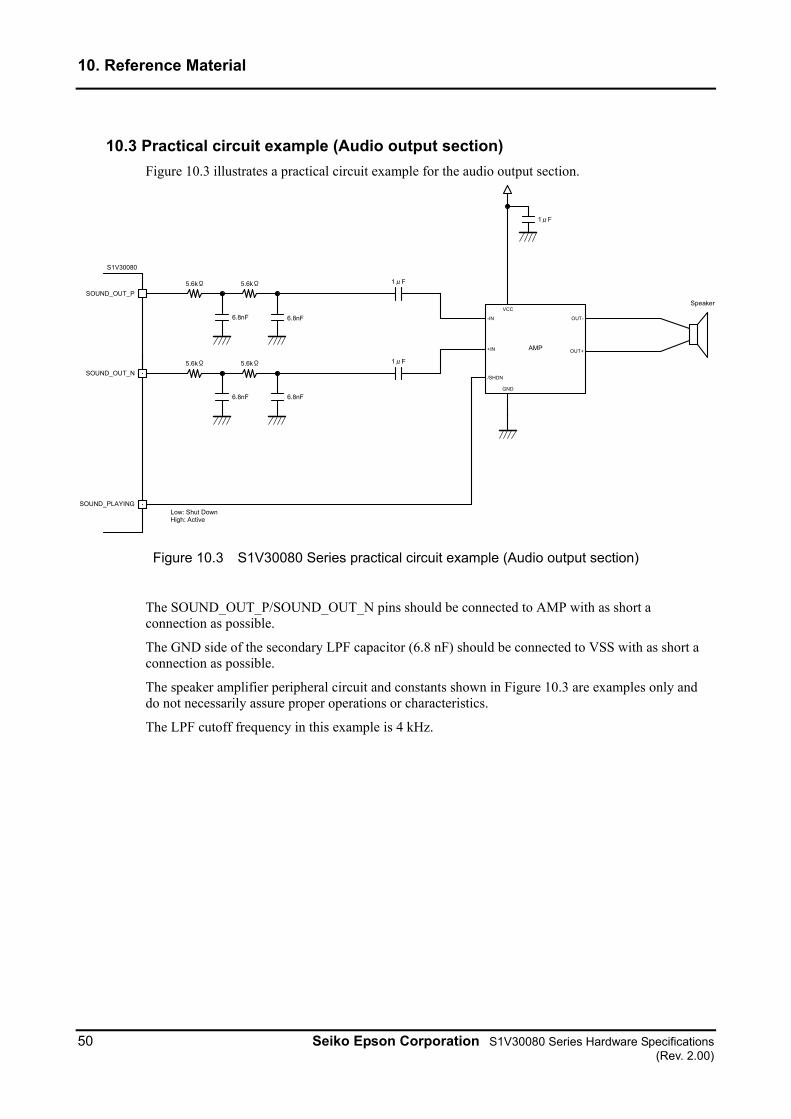
10.3 Practical circuit example (Audio output section)
Figure 10.3 illustrates a practical circuit example for the audio output section.
S1V30080
SOUND_OUT_P
5.6kΩ 5.6kΩ
6.8nF 6.8nF
1μF
-IN
GND
/SHDN
+IN
OUT-
OUT+AMP
Speaker
5.6kΩ 5.6kΩ
6.8nF 6.8nF
1μF
SOUND_OUT_N
SOUND_PLAYINGLow: Shut DownHigh: Active
VCC
1μF
Figure 10.3 S1V30080 Series practical circuit example (Audio output section)
The SOUND_OUT_P/SOUND_OUT_N pins should be connected to AMP with as short a connection as possible.
The GND side of the secondary LPF capacitor (6.8 nF) should be connected to VSS with as short a connection as possible.
The speaker amplifier peripheral circuit and constants shown in Figure 10.3 are examples only and do not necessarily assure proper operations or characteristics.
The LPF cutoff frequency in this example is 4 kHz.
10. Reference Material
S1V30080 Series Hardware Specifications Seiko Epson Corporation 51 (Rev. 2.00)
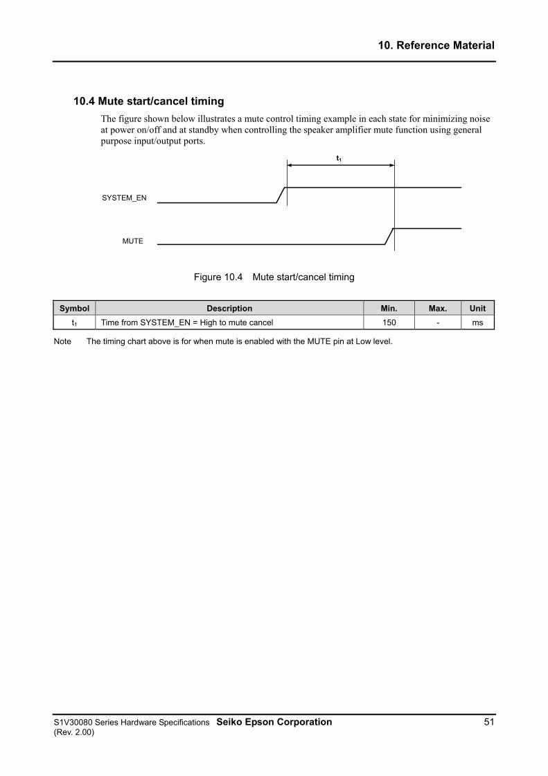
10.4 Mute start/cancel timing
The figure shown below illustrates a mute control timing example in each state for minimizing noise at power on/off and at standby when controlling the speaker amplifier mute function using general purpose input/output ports.
SYSTEM_EN
t1
MUTE
Figure 10.4 Mute start/cancel timing
Symbol Description Min. Max. Unit
t1 Time from SYSTEM_EN = High to mute cancel 150 - ms
Note The timing chart above is for when mute is enabled with the MUTE pin at Low level.
10. Reference Material
52 Seiko Epson Corporation S1V30080 Series Hardware Specifications (Rev. 2.00)
10.5 Precautions concerning power supply
Circuits should always be initialized using SYSTEM_EN after turning on power, since the state of the internal circuit cannot be guaranteed due to the effects of power supply noise when returning VDD from off to on.
CMOS-structured devices may enter what is called the “Latch-up” state. This involves current flowing through PNPN junctions (thyristor structures) inside the CMOS IC, resulting in large current flows between VDD and VSS and eventual damage.
Latch-ups occur when the voltage applied to the input and output pins exceeds the rating and a large current flows through the internal components, or when the VDD pin voltage exceeds the rating and internal components break down. The following points must be observed, since once a latch-up occurs, even if the voltage applied exceeds the rating only momentarily, a large current will be maintained between VDD and VSS, resulting in a risk of overheating or smoke generation.
(1) Do not raise voltage levels to the input and output pins beyond the range specified in the specifications for electrical characteristics or allow such levels to fall below VSS.
(2) Make sure the device is protected from exposure to excessive noise.
(3) Fix the electrical potential of unused input pins to VDD or VSS.
(4) Avoid short-circuiting the output.
10. Reference Material
S1V30080 Series Hardware Specifications Seiko Epson Corporation 53 (Rev. 2.00)
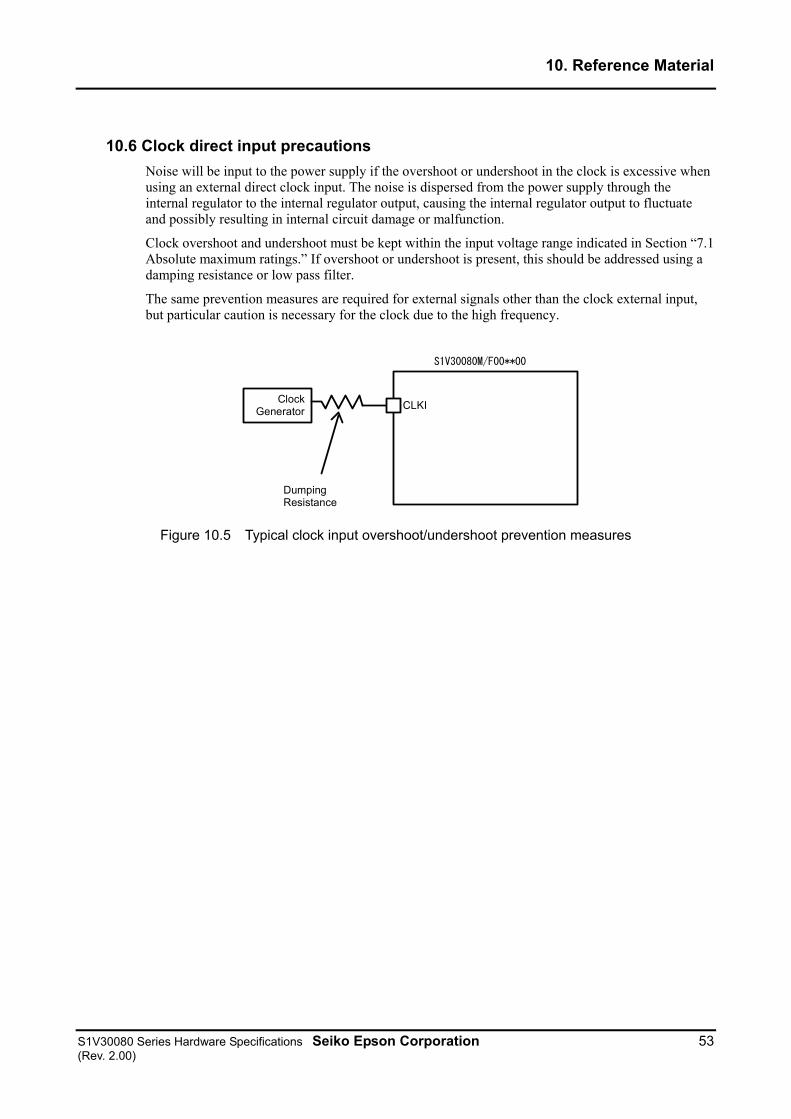
10.6 Clock direct input precautions
Noise will be input to the power supply if the overshoot or undershoot in the clock is excessive when using an external direct clock input. The noise is dispersed from the power supply through the internal regulator to the internal regulator output, causing the internal regulator output to fluctuate and possibly resulting in internal circuit damage or malfunction.
Clock overshoot and undershoot must be kept within the input voltage range indicated in Section “7.1 Absolute maximum ratings.” If overshoot or undershoot is present, this should be addressed using a damping resistance or low pass filter.
The same prevention measures are required for external signals other than the clock external input, but particular caution is necessary for the clock due to the high frequency.
S1V30080M/F00**00
CLKIClock
Generator
Dumping Resistance
Figure 10.5 Typical clock input overshoot/undershoot prevention measures
10. Reference Material
54 Seiko Epson Corporation S1V30080 Series Hardware Specifications (Rev. 2.00)
10.7 Mounting precautions
Observe the following precautions when designing the circuit board and mounting the IC.
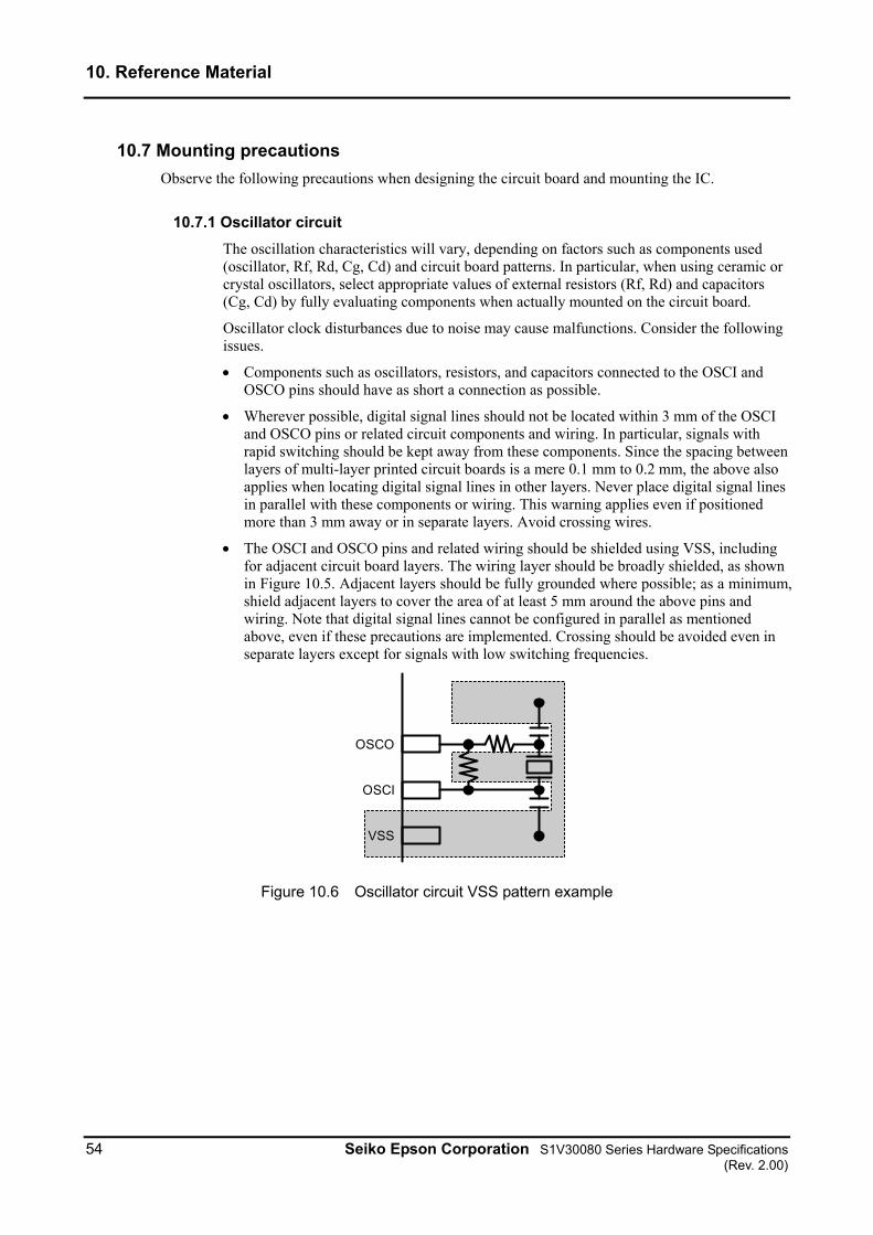
10.7.1 Oscillator circuit
The oscillation characteristics will vary, depending on factors such as components used (oscillator, Rf, Rd, Cg, Cd) and circuit board patterns. In particular, when using ceramic or crystal oscillators, select appropriate values of external resistors (Rf, Rd) and capacitors (Cg, Cd) by fully evaluating components when actually mounted on the circuit board.
Oscillator clock disturbances due to noise may cause malfunctions. Consider the following issues.
Components such as oscillators, resistors, and capacitors connected to the OSCI and OSCO pins should have as short a connection as possible.
Wherever possible, digital signal lines should not be located within 3 mm of the OSCI and OSCO pins or related circuit components and wiring. In particular, signals with rapid switching should be kept away from these components. Since the spacing between layers of multi-layer printed circuit boards is a mere 0.1 mm to 0.2 mm, the above also applies when locating digital signal lines in other layers. Never place digital signal lines in parallel with these components or wiring. This warning applies even if positioned more than 3 mm away or in separate layers. Avoid crossing wires.
The OSCI and OSCO pins and related wiring should be shielded using VSS, including for adjacent circuit board layers. The wiring layer should be broadly shielded, as shown in Figure 10.5. Adjacent layers should be fully grounded where possible; as a minimum, shield adjacent layers to cover the area of at least 5 mm around the above pins and wiring. Note that digital signal lines cannot be configured in parallel as mentioned above, even if these precautions are implemented. Crossing should be avoided even in separate layers except for signals with low switching frequencies.
VSS
OSCO
OSCI
Figure 10.6 Oscillator circuit VSS pattern example
10. Reference Material
S1V30080 Series Hardware Specifications Seiko Epson Corporation 55 (Rev. 2.00)
10.7.2 Reset circuit
The reset signal input to the SYSTEM_EN pin when power is turned on will vary, depending on various factors such as power supply rising time, components used, and circuit board patterns. Constants such as capacitance and resistance should be determined by testing thoroughly with practical products. You must account for resistance fluctuations when setting the SYSTEM_EN pin pull-up resistance since high impedance may cause malfunctions due to noise.
10.7.3 Power supply
Sudden power supply fluctuations due to noise will cause malfunctions. Always consider the following issues.
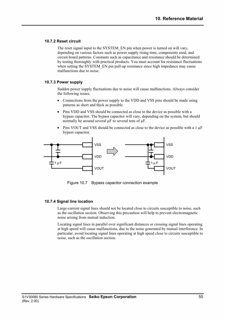
Connections from the power supply to the VDD and VSS pins should be made using patterns as short and thick as possible.
Pins VDD and VSS should be connected as close to the device as possible with a bypass capacitor. The bypass capacitor will vary, depending on the system, but should normally be around several µF to several tens of µF.
Pins VOUT and VSS should be connected as close to the device as possible with a 1 µF bypass capacitor.
VSS
VDD
VSS
VDD
VOUTVOUT
1μF1μF
Figure 10.7 Bypass capacitor connection example
10.7.4 Signal line location
Large-current signal lines should not be located close to circuits susceptible to noise, such as the oscillation section. Observing this precaution will help to prevent electromagnetic noise arising from mutual induction.
Locating signal lines in parallel over significant distances or crossing signal lines operating at high speed will cause malfunctions, due to the noise generated by mutual interference. In particular, avoid locating signal lines operating at high speed close to circuits susceptible to noise, such as the oscillation section.
10. Reference Material
56 Seiko Epson Corporation S1V30080 Series Hardware Specifications (Rev. 2.00)
10.7.5 Malfunction due to noise
Check the following points if you suspect IC malfunctions due to noise.
SYSTEM_EN pin Low-level noise to this pin will reset the IC. However, the reset may not execute properly, depending on the input waveform. This is more likely to occur if the impedance is high when the reset input is High due to factors related to circuit design.
SCKS pin This pin is the synchronized clock input pin for the clock synchronized serial interface. Exposing this pin to noise may cause waveforms to be identified as valid data, resulting in malfunctions. Make the serial interface (SCKS, SIS, SOS) connections as short as possible.
FLASH_SCKM pin This pin is the synchronized clock output pin for the clock synchronized serial interface. Noise accompanying signals output from this pin may be mistakenly identified as valid data by the external serial flash memory, resulting in malfunctions.
Large load capacitance in output from this pin will increase delays at the external serial flash memory interface, exceeding specifications for FLASH_SIM setup time. (Refer to “7.4.10 External serial flash memory access timing.”)
The external serial flash memory interface (FLASH_SCKM, FLASH_SIM, FLASH_SOM, FLASH_NSCSM) connections should be made as short as possible.
Power supply The IC will malfunction the instant noise deviating from the specified voltage is input. Countermeasures should be provided on the circuit board, such as solid patterns for circuit board power supply circuits and adding noise-filtering decoupling capacitors and surge/noise prevention components to the power supply line.
10.7.6 Miscellaneous
The S1V30080 Series is manufactured using a 0.15 µm microscopic process. It is designed to ensure basic IC reliability meeting EIAJ and MIL standards, but care must be taken with respect to the following points when mounting the product.
The OSCI and OSCO pins directly use internal 0.15 µm transistors. In addition to potential physical damage during mounting, products may also be electrically damaged by disturbances in the form of voltages exceeding the absolute maximum rating (2.5 V) due to gradual variations over time. These include the following:
Electromagnetic noise generated by industrial power supplies used in mounting reflow, reworking after mounting, and individual characteristic evaluation (testing) processes
Electromagnetic noise from a solder iron when soldering
In particular, during soldering, the soldering iron GND (tip potential) should be at the same potential as the IC GND.
10. Reference Material
S1V30080 Series Hardware Specifications Seiko Epson Corporation 57 (Rev. 2.00)
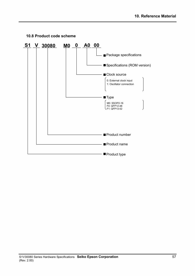
10.8 Product code scheme
M0: SSOP2-16F0: QFP12-48F1: QFP13-52
S1 V 30080 M0 A00 00
梱包仕様
仕様(ROM Version)
クロック源
0 : 外部クロック入力1 : 振動子接続
形状
機種番号
機種名称
製品分類
Product number
Product name
Product type
Type
Clock source
Specifications (ROM version)
Package specifications
0: External clock input 1: Oscillator connection
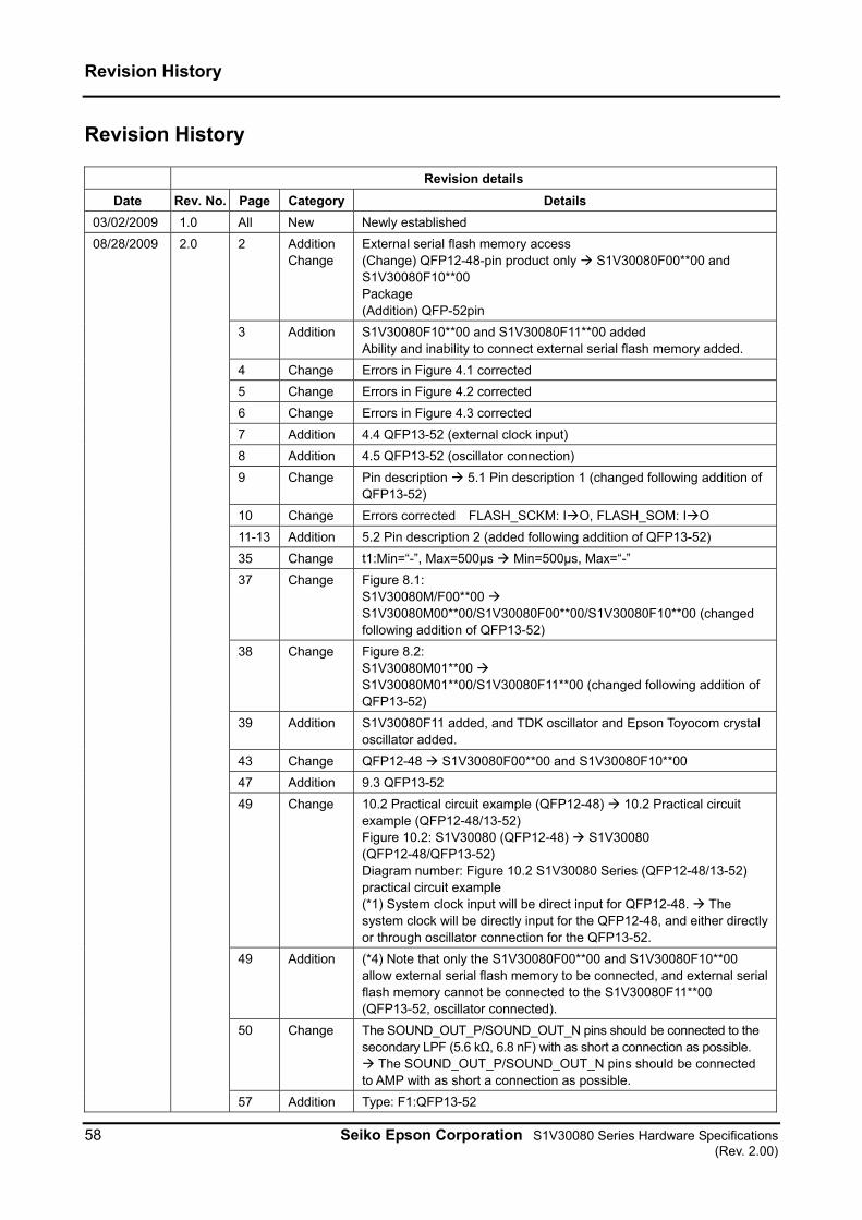
Revision History
58 Seiko Epson Corporation S1V30080 Series Hardware Specifications (Rev. 2.00)
Revision History
Revision details
Date Rev. No. Page Category Details
03/02/2009 1.0 All New Newly established
2 Addition Change
External serial flash memory access (Change) QFP12-48-pin product only S1V30080F00**00 and S1V30080F10**00 Package (Addition) QFP-52pin
3 Addition S1V30080F10**00 and S1V30080F11**00 added Ability and inability to connect external serial flash memory added.
4 Change Errors in Figure 4.1 corrected
5 Change Errors in Figure 4.2 corrected
6 Change Errors in Figure 4.3 corrected
7 Addition 4.4 QFP13-52 (external clock input)
8 Addition 4.5 QFP13-52 (oscillator connection)
9 Change Pin description 5.1 Pin description 1 (changed following addition of QFP13-52)
10 Change Errors corrected FLASH_SCKM: IO, FLASH_SOM: IO
11-13 Addition 5.2 Pin description 2 (added following addition of QFP13-52)
35 Change t1:Min=“-”, Max=500μs Min=500μs, Max=“-”
37 Change Figure 8.1: S1V30080M/F00**00 S1V30080M00**00/S1V30080F00**00/S1V30080F10**00 (changed following addition of QFP13-52)
38 Change Figure 8.2: S1V30080M01**00 S1V30080M01**00/S1V30080F11**00 (changed following addition of QFP13-52)
39 Addition S1V30080F11 added, and TDK oscillator and Epson Toyocom crystal oscillator added.
43 Change QFP12-48 S1V30080F00**00 and S1V30080F10**00
47 Addition 9.3 QFP13-52
49 Change 10.2 Practical circuit example (QFP12-48) 10.2 Practical circuit example (QFP12-48/13-52) Figure 10.2: S1V30080 (QFP12-48) S1V30080 (QFP12-48/QFP13-52) Diagram number: Figure 10.2 S1V30080 Series (QFP12-48/13-52) practical circuit example (*1) System clock input will be direct input for QFP12-48. The system clock will be directly input for the QFP12-48, and either directly or through oscillator connection for the QFP13-52.
49 Addition (*4) Note that only the S1V30080F00**00 and S1V30080F10**00 allow external serial flash memory to be connected, and external serial flash memory cannot be connected to the S1V30080F11**00 (QFP13-52, oscillator connected).
50 Change The SOUND_OUT_P/SOUND_OUT_N pins should be connected to the secondary LPF (5.6 kΩ, 6.8 nF) with as short a connection as possible. The SOUND_OUT_P/SOUND_OUT_N pins should be connected to AMP with as short a connection as possible.
08/28/2009 2.0
57 Addition Type: F1:QFP13-52
International Sales Operations
AMERICA EPSON ELECTRONICS AMERICA, INC. 2580 Orchard Parkway,
San Jose, CA 95131, USA
Phone: +1-800-228-3964 FAX: +1-408-922-0238
EUROPE EPSON EUROPE ELECTRONICS GmbH Riesstrasse 15, 80992 Munich,
GERMANY
Phone: +49-89-14005-0 FAX: +49-89-14005-110
ASIA EPSON (CHINA) CO., LTD. 7F, Jinbao Bldg., No.89 Jinbao St., Dongcheng District, Beijing 100005, CHINA Phone: +86-10-6410-6655 FAX: +86-10-6410-7320
SHANGHAI BRANCH 7F, Block B, Hi-Tech Bldg., 900 Yishan Road, Shanghai 200233, CHINA Phone: +86-21-5423-5522 FAX: +86-21-5423-5512
SHENZHEN BRANCH 12F, Dawning Mansion, Keji South 12th Road, Hi-Tech Park, Shenzhen 518057, CHINA Phone: +86-755-2699-3828 FAX: +86-755-2699-3838 EPSON HONG KONG LTD. 20/F, Harbour Centre, 25 Harbour Road, Wanchai, Hong Kong Phone: +852-2585-4600 FAX: +852-2827-4346 Telex: 65542 EPSCO HX EPSON TAIWAN TECHNOLOGY & TRADING LTD. 14F, No. 7, Song Ren Road, Taipei 110, TAIWAN Phone: +886-2-8786-6688 FAX: +886-2-8786-6660 EPSON SINGAPORE PTE., LTD. 1 HarbourFront Place,
#03-02 HarbourFront Tower One, Singapore 098633 Phone: +65-6586-5500 FAX: +65-6271-3182 SEIKO EPSON CORP. KOREA OFFICE 50F, KLI 63 Bldg., 60 Yoido-dong, Youngdeungpo-Ku, Seoul 150-763, KOREA Phone: +82-2-784-6027 FAX: +82-2-767-3677
SEIKO EPSON CORP. SEMICONDUCTOR OPERATIONS DIVISION IC Sales Dept. IC International Sales Group 421-8, Hino, Hino-shi, Tokyo 191-8501, JAPAN Phone: +81-42-587-5814 FAX: +81-42-587-5117
Document Code: 411679001 First Issue March 2009
Revised August 2009 in JAPAN D
Related Documents