S. Reda EN160 SP’08 esign and Implementation of VLSI System (EN01600) ecture 19: Combinational Circuit Design (1/3 Prof. Sherief Reda Division of Engineering, Brown University Spring 2008 [sources: Weste/Addison Wesley – Rabaey/Pearson]

S. Reda EN160 SP’08 Design and Implementation of VLSI Systems (EN01600) Lecture 19: Combinational Circuit Design (1/3) Prof. Sherief Reda Division of Engineering,
Dec 18, 2015
Welcome message from author
This document is posted to help you gain knowledge. Please leave a comment to let me know what you think about it! Share it to your friends and learn new things together.
Transcript

S. Reda EN160 SP’08
Design and Implementation of VLSI Systems(EN01600)
Lecture 19: Combinational Circuit Design (1/3)
Prof. Sherief RedaDivision of Engineering, Brown University
Spring 2008
[sources: Weste/Addison Wesley – Rabaey/Pearson]
S. Reda EN160 SP’08
Circuit Families
1.Static CMOS2.Ratioed Circuits3.Cascode Voltage Switch Logic4.Dynamic Circuits5.Pass-transistor Circuits

S. Reda EN160 SP’08
1. Static CMOS
• Start with network of AND / OR gates• Convert to NAND / NOR + inverters• Push bubbles around to simplify logic
– Remember DeMorgan’s Law
Y Y
Y
D
Y
(a) (b)
(c) (d)
S. Reda EN160 SP’08
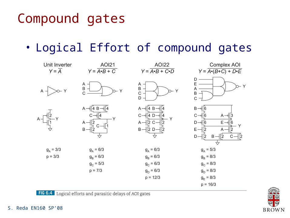
Compound gates
• Logical Effort of compound gates
S. Reda EN160 SP’08
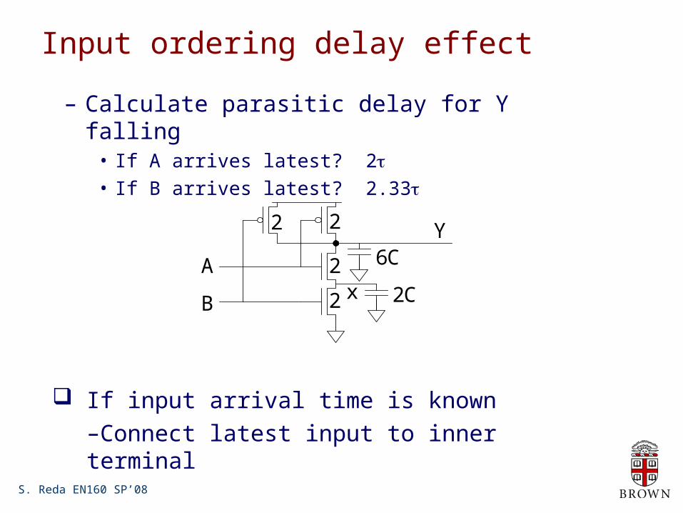
Input ordering delay effect
– Calculate parasitic delay for Y falling• If A arrives latest? 2• If B arrives latest? 2.33
6C
2C2
2
22
B
Ax
Y
If input arrival time is known–Connect latest input to inner terminal

S. Reda EN160 SP’08
Asymmetric gates
• Asymmetric gates favor one input over another• Ex: suppose input A of a NAND gate is most critical
– Use smaller transistor on A (less capacitance)– Boost size of noncritical input– So total resistance is same
• gA = 10/9
• gB = 2
• gavg = (gA + gB)/2 = 14/9
• Asymmetric gate approaches g = 1 on critical input• But total logical effort goes up

S. Reda EN160 SP’08
Symmetric gates
• Inputs can be made perfectly symmetric
A
B
Y2
1
1
2
1
1
S. Reda EN160 SP’08
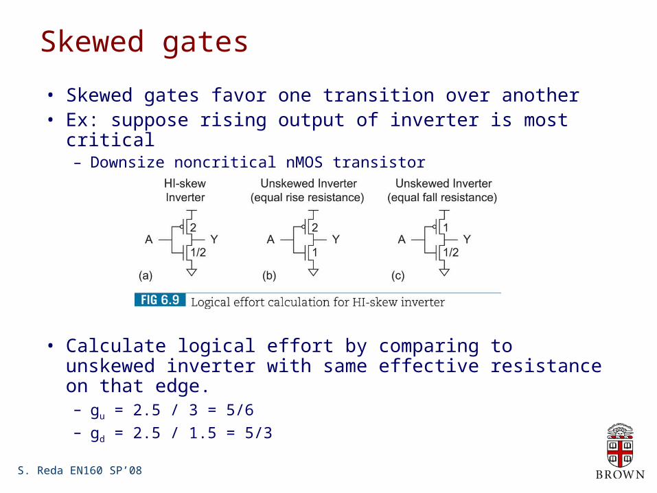
Skewed gates
• Skewed gates favor one transition over another• Ex: suppose rising output of inverter is most critical
– Downsize noncritical nMOS transistor
• Calculate logical effort by comparing to unskewed inverter with same effective resistance on that edge.– gu = 2.5 / 3 = 5/6– gd = 2.5 / 1.5 = 5/3

S. Reda EN160 SP’08
Hi- and Lo-Skew
• Definition: Logical effort of a skewed gate for a particular transition is the ratio of the input capacitance of the skewed gate to the input capacitance of an unskewed inverter with equal drive for the same transition.
• Skewed gates reduce size of noncritical transistors– HI-skew gates favor rising output (small nMOS)– LO-skew gates favor falling output (small pMOS)
• Logical effort is smaller for favored direction• But larger for the other direction

S. Reda EN160 SP’08
Catalog of skewed gates
S. Reda EN160 SP’08
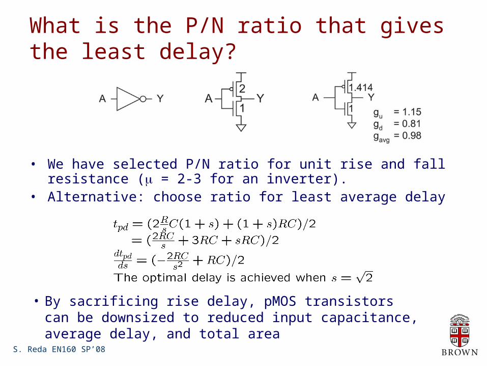
What is the P/N ratio that gives the least delay?
• We have selected P/N ratio for unit rise and fall resistance ( = 2-3 for an inverter).
• Alternative: choose ratio for least average delay
• By sacrificing rise delay, pMOS transistors can be downsized to reduced input capacitance, average delay, and total area

S. Reda EN160 SP’08
Beware of PMOS
• pMOS is the enemy!– High input and diffusion capacitance for a given current
• Can we take the pMOS capacitance off the input?– Various circuit families try to do this…
B
A
11
4
4
Y
Related Documents