R01DS0228EJ0110 Rev.1.10 Page 1 of 132 Jul 08, 2016 RZ/T1 Group Datasheet Features ■ On-chip 32-bit ARM Cortex-R4F processor • High-speed realtime control with maximum operating frequency of 300/450/600 MHz Capable of 498/747/996 DMIPS (in operation at 300/450/600 MHz) • On-chip 32-bit ARM Cortex-R4F (revision r1p4) • Tightly coupled memory (TCM) with ECC: 512 Kbytes/32 Kbytes • Instruction cache/data cache with ECC: 8 Kbytes per cache • High-speed interrupt • The FPU supports addition, subtraction, multiplication, division, multiply-and-accumulate, and square-root operations at single- precision and double-precision. • Harvard architecture with 8-stage pipeline • Supports the memory protection unit (MPU) • ARM CoreSight architecture, includes support for debugging through JTAG and SWD interfaces ■ On-chip 32-bit ARM Cortex-M3 processor (in products incorporating an R-IN engine) • 150-MHz operating frequency • On-chip 32-bit ARM Cortex-M3 (revision r2p1) • RISC Harvard architecture with 3-stage pipeline • Supports the memory protection unit (MPU) ■ Low power consumption • Standby mode, sleep mode, and module stop function ■ On-chip extended SRAM • Up to 1 Mbyte of the on-chip extended SRAM with ECC • 150 MHz ■ Data transfer • DMAC: 16 channels × 2 units • DMAC for the Ethernet controller: 1 channel ■ Event link controller • Module operations can be started by event signals rather than by interrupt handlers. • Linked operation of modules is available even while the CPU is in the sleep state. ■ Reset and power supply voltage control • Four reset sources including a pin reset • Dual power-voltage configuration: 3.3 V (I/O unit), 1.2 V (internal) ■ Clock functions • External clock/oscillator input frequency: 25 MHz • CPU clock frequency: Up to 300/450/600 MHz • Low-speed on-chip oscillator (LOCO): 240 kHz ■ Independent watchdog timer • Operated by a clock signal obtained by frequency-dividing the clock signal from the low-speed on-chip oscillator: Up to 120 kHz ■ Safety functions • Register write protection, input clock oscillation stop detection, CRC, IWDTa, and A/D self-diagnosis • An error control module is incorporated to generate a pin signal output, interrupt, or internal reset in response to errors originating in the various modules. ■ Security functions (optional)* 2 • Boot mode with security through encryption ■ Encoder interfaces (optional)* 3 • EnDat 2.2 and BiSS-compliant interfaces* 4 ■ Various communications interfaces • Ethernet - EtherCAT slave controller: 2 ports (optional) - Ether-MAC: 1 port (without the switching function) or - Ether-MAC: 1 port (2 ports with the switching function) • USB 2.0 high-speed host/function : 1 channel • CAN (compliant with ISO11898-1): 2 channels (max.) • SCIFA with 16-byte transmission and reception FIFOs: 5 channels • I 2 C bus interface: 2 channels for transfer at up to 400 kbps • RSPIa: 4 channels • SPIBSC: Provides a single interface for multi-I/O compatible serial flash memory ■ External address space • Buses for high-speed data transfer at 75 MHz (max.) • Support for up to 6 CS areas • 8-, 16-, or 32-bit bus space is selectable per area ■ Up to 33 extended-function timers • 16-bit TPUa (12 channels), MTU3a (9 channels), GPTa (4 channels): Input capture, output compare, PWM waveform output • 16-bit CMT (6 channels), 32-bit CMTW (2 channels) ■ Serial sound interface (1 channel) ■ ∆Σ interface • Up to 4 ΔΣ modulators are connectable externally. ■ 12-bit A/D converters • 12 bits × 2 units (max.) (8 channels for unit 0; 16 channels for unit 1) • Self diagnosis • Detection of analog input disconnection ■ Temperature sensor for measuring temperature within the chip ■ General-purpose I/O ports • 5-V tolerance, open drain, input pull-up ■ Multi-function pin controller • The locations of input/output functions for peripheral modules are selectable from among multiple pins. ■ Operating temperature range • Tj = -40°C to +125°C Tj: Junction temperature PRBG0320GA-A 17×17mm, 0.8-mm pitch PLQP0176LD-A 20 x 20mm, 0.4-mm pitch 300 MHz/450 MHz/600 MHz, MCU with ARM Cortex ® -R4F and -M3* 1 , on-chip FPU, 498/747/996 DMIPS, up to 1 Mbyte of on-chip extended SRAM, Ethernet MAC, EtherCAT* 1 , USB 2.0 high-speed, CAN, various communications interfaces such as an SPI multi-I/O bus controller, ∆Σ interface, safety functions, encoder interfaces* 1 , and security functions* 1 R01DS0228EJ0110 Rev.1.10 Jul 08, 2016 Note 1. Optional Note 2. Details of these optional functions will only be disclosed after completion of a binding non-disclosure agreement. For details, contact our sales representative. Note 3. For details, contact our sales representative. Note 4. BiSS is a registered trademark of iC-Haus GmbH.

Welcome message from author
This document is posted to help you gain knowledge. Please leave a comment to let me know what you think about it! Share it to your friends and learn new things together.
Transcript

R01DS0228EJ0110 Rev.1.10 Page 1 of 132Jul 08, 2016
RZ/T1 Group
Datasheet
Features On-chip 32-bit ARM Cortex-R4F processor
• High-speed realtime control with maximum operating frequency of 300/450/600 MHzCapable of 498/747/996 DMIPS (in operation at 300/450/600 MHz)
• On-chip 32-bit ARM Cortex-R4F (revision r1p4)• Tightly coupled memory (TCM) with ECC: 512 Kbytes/32 Kbytes• Instruction cache/data cache with ECC: 8 Kbytes per cache• High-speed interrupt• The FPU supports addition, subtraction, multiplication, division,
multiply-and-accumulate, and square-root operations at single-precision and double-precision.
• Harvard architecture with 8-stage pipeline• Supports the memory protection unit (MPU)• ARM CoreSight architecture, includes support for debugging
through JTAG and SWD interfaces
On-chip 32-bit ARM Cortex-M3 processor (in products incorporating an R-IN engine)
• 150-MHz operating frequency• On-chip 32-bit ARM Cortex-M3 (revision r2p1)• RISC Harvard architecture with 3-stage pipeline• Supports the memory protection unit (MPU)
Low power consumption• Standby mode, sleep mode, and module stop function
On-chip extended SRAM• Up to 1 Mbyte of the on-chip extended SRAM with ECC• 150 MHz
Data transfer• DMAC: 16 channels × 2 units• DMAC for the Ethernet controller: 1 channel
Event link controller• Module operations can be started by event signals rather than by
interrupt handlers. • Linked operation of modules is available even while the CPU is in
the sleep state.
Reset and power supply voltage control• Four reset sources including a pin reset• Dual power-voltage configuration: 3.3 V (I/O unit), 1.2 V
(internal)
Clock functions• External clock/oscillator input frequency: 25 MHz• CPU clock frequency: Up to 300/450/600 MHz• Low-speed on-chip oscillator (LOCO): 240 kHz
Independent watchdog timer• Operated by a clock signal obtained by frequency-dividing the
clock signal from the low-speed on-chip oscillator: Up to 120 kHz
Safety functions• Register write protection, input clock oscillation stop detection,
CRC, IWDTa, and A/D self-diagnosis• An error control module is incorporated to generate a pin signal
output, interrupt, or internal reset in response to errors originating in the various modules.
Security functions (optional)*2
• Boot mode with security through encryption
Encoder interfaces (optional)*3
• EnDat 2.2 and BiSS-compliant interfaces*4
Various communications interfaces• Ethernet
- EtherCAT slave controller: 2 ports (optional)- Ether-MAC: 1 port (without the switching function)or- Ether-MAC: 1 port (2 ports with the switching function)
• USB 2.0 high-speed host/function : 1 channel• CAN (compliant with ISO11898-1): 2 channels (max.)• SCIFA with 16-byte transmission and reception FIFOs: 5 channels• I2C bus interface: 2 channels for transfer at up to 400 kbps• RSPIa: 4 channels• SPIBSC: Provides a single interface for multi-I/O compatible
serial flash memory
External address space• Buses for high-speed data transfer at 75 MHz (max.)• Support for up to 6 CS areas• 8-, 16-, or 32-bit bus space is selectable per area
Up to 33 extended-function timers• 16-bit TPUa (12 channels), MTU3a (9 channels), GPTa (4
channels): Input capture, output compare, PWM waveform output• 16-bit CMT (6 channels), 32-bit CMTW (2 channels)
Serial sound interface (1 channel)
∆Σ interface• Up to 4 ΔΣ modulators are connectable externally.
12-bit A/D converters• 12 bits × 2 units (max.)
(8 channels for unit 0; 16 channels for unit 1)• Self diagnosis• Detection of analog input disconnection
Temperature sensor for measuring temperature within the chip
General-purpose I/O ports• 5-V tolerance, open drain, input pull-up
Multi-function pin controller• The locations of input/output functions for peripheral modules are
selectable from among multiple pins.
Operating temperature range• Tj = -40°C to +125°C
Tj: Junction temperature
PRBG0320GA-A 17×17mm, 0.8-mm pitch
PLQP0176LD-A 20 x 20mm, 0.4-mm pitch
300 MHz/450 MHz/600 MHz, MCU with ARM Cortex®-R4F and -M3*1, on-chip FPU, 498/747/996 DMIPS, up to 1 Mbyte of on-chip extended SRAM, Ethernet MAC, EtherCAT*1, USB 2.0 high-speed, CAN, various communications interfaces such as an SPI multi-I/O bus controller, ∆Σ interface, safety functions, encoder interfaces*1, and security functions*1
R01DS0228EJ0110Rev.1.10
Jul 08, 2016
Note 1. OptionalNote 2. Details of these optional functions will only be disclosed after completion of a binding non-disclosure agreement. For details, contact our sales
representative.Note 3. For details, contact our sales representative.Note 4. BiSS is a registered trademark of iC-Haus GmbH.

R01DS0228EJ0110 Rev.1.10 Page 2 of 132Jul 08, 2016
RZ/T1 Group 1. Overview
1. Overview
1.1 Outline of Specifications
This LSI circuit is a high-performance MCU equipped with the ARM Cortex®-R4F processor and Cortex-M3 (for
products incorporating an R-IN engine) processors, and incorporating integrated peripheral functions necessary for
system configuration. Table 1.1 lists the specifications in outline, and Table 1.2 gives a comparison of the functions of
products in different packages.
Table 1.1 shows the outline of maximum specifications, and the number of peripheral module channels differs
depending on the pin number on the package. For details, see Table 1.2, Comparison of Functions for Different
Packages.
Table 1.1 Outline of Specifications (1 / 7)
Classification Module/Function Description
CPU Central processing unit (Cortex-R4F)
• Maximum operating frequency320-pin FBGA: 300 MHz/450 MHz/600 MHz176-pin HLQFP: 450 MHz
• 32-bit CPU Cortex-R4F designed by ARM (core revision r1p4)• Address space: 4 Gbytes• Instruction cache: 8 Kbytes (with ECC)• Data cache: 8 Kbytes (with ECC)• Tightly coupled memory (TCM)
ATCM: 512 Kbytes (with ECC)BTCM: 32 Kbytes (with ECC)
• Instruction set: ARMv7-R architecture, so support includes Thumb and Thumb-2• Data arrangement
Instructions: Little endianData: Little endian
• Memory protection unit (MPU)
Central processing unit (Cortex-M3)(for products incorporating an R-IN engine)
• Operating frequency: 150 MHz• 32-bit CPU Cortex-M3 designed by ARM (core revision r2p1)• Address space: 4 Gbytes• Instruction set: ARMv7-R architecture, so support includes Thumb® and Thumb-2• Data arrangement
Instructions: Little endianData: Little endian
• Memory protection unit (MPU)
FPU(Cortex-R4F)
• Supports addition, subtraction, multiplication, division, multiply-and-accumulate, and square-root operations at single- and double-precision.
• Registers32-bit single-word registers: 32 bits ×32(can be used as 16 double-word registers: 64 bits x 16)
Memory On-chip extended SRAM with ECC
• Capacity: Up to 1 Mbyte• 150 MHz• SEC-DED (single error correction/double error detection)
Operating modes • Three boot modesSPI boot mode (for booting up from serial flash memory)16-bit bus boot mode (NOR Flash)32-bit bus boot mode (NOR Flash)
Clock Clock generation circuit • The input clock can be selected from an external clock signal or external resonator.• Detection of input clock oscillation stopping• The following clocks are generated.
CPU clock: 300/450/600 MHz (max.)System clock: 150 MHz (fixed)High-speed peripheral module clock: 150 MHz (fixed)Low-speed peripheral module clock: 75 MHz (fixed)ADCCLK in the 12-bit A/D converter (S12ADCa): 60 MHz (max.)External bus clock: 75 MHz (max.)Low-speed on-chip oscillator: 240 kHz (fixed)
Reset RES # pin reset, error control module (ECM) reset, software reset
R01DS0228EJ0110 Rev.1.10 Page 3 of 132Jul 08, 2016
RZ/T1 Group 1. Overview
Low power Low power consumption • Standby mode (Cortex-R4F)• Sleep mode (Cortex-M3) (for products incorporating an R-IN engine)• Module stop function
Interrupt Cortex-R4Fvector interrupt controller (VIC)
• Peripheral function interrupts: 273 sources / 276 sources (for products incorporating an R-IN engine)
• External interrupts: 20 sources(NMI, IRQ0 to IRQ15, ETH0_INT, ETH1_INT, and ETH2_INT pins)
• Software interrupts: 1 source• Non-maskable interrupts: 2 sources• Sixteen levels specifiable for the order of priority
Cortex-M3 nested-type vector interrupt controller (NVIC)(only included in products incorporating an R-IN engine)
• Peripheral function interrupts: 82 sources• External interrupts: 19 sources
(IRQ0 to IRQ15, ETH0_INT, ETH1_INT, and ETH2_INT pins)• Software interrupts: 1 source• Non-maskable interrupts: 1 source• Sixteen levels specifiable for the order of priority
External bus extension
Bus state controller (BSC)
• The external address space is divided into six areas (CS0 to CS5) for management.• The following features settable for each area independently.
Bus size (8, 16, or 32 bits): Available sizes depend on the area.Number of access wait cycles (different wait cycles can be specified for read and write access cycles in some areas)Idle wait cycle insertion (between same area access cycles or different area access cycles)Specifying the memory to be connected to each area enables direct connection to SRAM, SRAM with byte selection, SDRAM, and burst ROM (clocked synchronous or asynchronous). The address/data multiplexed I/O (MPX) interface is also available.
• Outputs a chip select signal (CS0# to CS5#) according to the target area (CS assert or negate timing can be selected by software)
• SDRAM refreshAuto refresh or self-refresh mode selectable
• SDRAM burst access
Data transfer Direct memory access controller (DMAC)
• 2 units (16 channels for unit 0, 16 channels for unit 1)• Transfer modes: Single transfer mode and block transfer mode• Transfer size
Unit 0: 1/2/4/16/32/64 bytesUnit 1: 1/2/4/16 bytes
• Activation sources: Software trigger, external DMA requests (DREQ0 to DREQ2), external interrupts, and interrupt requests from peripheral functions
I/O ports General-purpose I/O ports
• 320-pin FBGAI/O pins: 209Input pins: 9Pull-up/pull-down resistors: 2095-V tolerance: 9
• 176-pin HLQFPI/O pins: 97Input pins: 5 Pull-up/pull-down resistors: 975-V tolerance: 5
Event link controller (ELC) • 87 event signals can be interlinked with the operation of modules.• In particular, the operation of timer modules can be started by input event signals.• Event-linked operation of signals of ports B and E is to be possible.
Multi-function pin controller (MPC) The locations of input/output functions are selectable from among multiple pins.
Table 1.1 Outline of Specifications (2 / 7)
Classification Module/Function Description
R01DS0228EJ0110 Rev.1.10 Page 4 of 132Jul 08, 2016
RZ/T1 Group 1. Overview
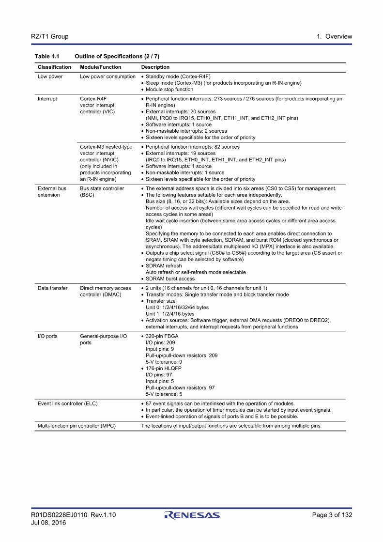
Timers 16-bit timer pulse unit (TPUa)
• (16 bits × 6 channels) × 2 units*1
• Maximum of 32 pulse-input/output possible• Select from among seven or eight counter-input clock signals for each channel
(with maximum operating frequency of 75 MHz)• Input capture/output compare function• Counter clear operation (synchronous clearing by compare match/input capture)• Simultaneous writing to multiple timer counters (TCNT)• Simultaneous register input/output by synchronous counter operation• Output of PWM waveforms in up to 30 phases in PWM mode• Support for buffered operation, phase-counting mode (two phase encoder input) and
cascade-connected operation (32 bits × 4 channels) depending on the channel.• PPG output trigger can be generated• Capable of generating conversion start triggers for the A/D converters• Digital noise filtering of signals from the input capture pins• Event linking by the ELC
Multifunction timer pulse unit (MTU3a)
• 9 channels (16 bits × 8 channels, 32 bits × 1 channel)• Maximum of 28 pulse-input/output and 3 pulse-input possible• Select from among 9, 11, or 12 counter-input clock signals for each channel
(with maximum operating frequency of 150 MHz)• Input capture function• 39 output compare/input capture registers• Counter clear operation (synchronous clearing by compare match/input capture)• Simultaneous writing to multiple timer counters (TCNT)• Simultaneous register input/output by synchronous counter operation• Buffered operation• Support for cascade-connected operation• Automatic transfer of register data• Pulse output mode
Toggle/PWM/complementary PWM/reset-synchronized PWM• Complementary PWM output mode
Outputs non-overlapping waveforms for controlling 3-phase invertersAutomatic specification of dead timesPWM duty cycle: Selectable as any value from 0% to 100%Delay can be applied to requests for A/D conversion.Non-generation of interrupt requests at peak or trough values of counters can be selected.Double buffer configuration
• Reset synchronous PWM modeThree phases of positive and negative PWM waveforms can be output with desired duty cycles.
• Phase-counting mode: 16-bit mode (channels 1 and 2); 32-bit mode (channels 1 and 2)• Counter functionality for dead-time compensation• Generation of triggers for A/D converter conversion• A/D converter start triggers can be skipped• Digital noise filter function for signals on the input capture and external counter clock
pins• PPG output trigger can be generated• Event linking by the ELC
Table 1.1 Outline of Specifications (3 / 7)
Classification Module/Function Description

R01DS0228EJ0110 Rev.1.10 Page 5 of 132Jul 08, 2016
RZ/T1 Group 1. Overview
Timers General PWM timer (GPTa)
• 16 bits × 4 channels• Counting up or down (saw-wave), counting up and down (triangle-wave) selectable for
all channels• Select from among four counter-input clock signals for each channel
(with maximum operating frequency of 150 MHz)• 2 input/output pins per channel• 2 output compare/input capture registers per channel• For the 2 output compare/input capture registers of each channel, 4 registers are
provided as buffer registers and are capable of operating as comparison registers when buffering is not in use.
• In output compare operation, buffer switching can be at peaks or troughs, enabling the generation of laterally asymmetrically PWM waveforms.
• Registers for setting up frame intervals on each channel (with capability for generating interrupts on overflow or underflow)
• Synchronizable operation of the several counters• Modes of synchronized operation (synchronized, or displaced by desired times for
phase shifting)• Generation of dead times in PWM operation• Through combination of three counters, generation of automatic three-phase PWM
waveforms incorporating dead times• Starting, clearing, and stopping counters in response to external or internal triggers• Internal trigger sources: software, and compare-match• Generation of triggers for A/D converter conversion• Digital noise filter function for signals on the input capture and external trigger pins• Event linking by the ELC
Programmable pulse generator (PPG)
• (4 bits × 4 groups) × 2 units*1
• Pulse output with the MTU3a or TPUa output as a trigger• Maximum of 32 pulse-output possible
Compare match timer (CMT)
• (16 bits × 2 channels) × 3 units• Select from among four counter-input clock signals for each channel (with maximum
operating frequency of 75 MHz)• Event linking by the ELC
Compare match timer W (CMTW)
• (32 bits × 1 channel) × 2 units• Compare-match, input-capture input, and output-comparison output are available.• Select from among four counter-input clock signals for each channel (with maximum
operating frequency of 75 MHz)• Interrupt requests can be output in response to compare-match, input-capture, and
output-comparison events.• Digital noise filter function for signals on the input capture pins• Event linking by the ELC
Watchdog timer (WDTA) • 14 bits × 1 channelProducts incorporating an R-IN engine: 14 bits × 2 channels
• Select from among six counter-input clock signals for each channel (with maximum operating frequency of 75 MHz)
Independent watchdog timer (IWDTa)
• 14 bits × 1 channel• Counter-input clock: Low-speed on-chip oscillator (LOCO)/2
Dedicated clock/1, dedicated clock/16, dedicated clock/32, dedicated clock/64, dedicated clock/128, dedicated clock/256 (with maximum operating frequency of 120 MHz)
Port output enable 3 (POE3)
• Control of the high-impedance state of the MTU3a / GPTa's waveform output pins• 4 pins for input from signal sources: POE0, POE4, POE8, POE10• Initiation on detection of short-circuited outputs (detection of simultaneous PWM output
to the active level)• Initiation by input clock oscillation-stoppage detection, PLL oscillation anomaly
detection, or software• Additional programming of output control target pins is enabled
Table 1.1 Outline of Specifications (4 / 7)
Classification Module/Function Description
R01DS0228EJ0110 Rev.1.10 Page 6 of 132Jul 08, 2016
RZ/T1 Group 1. Overview
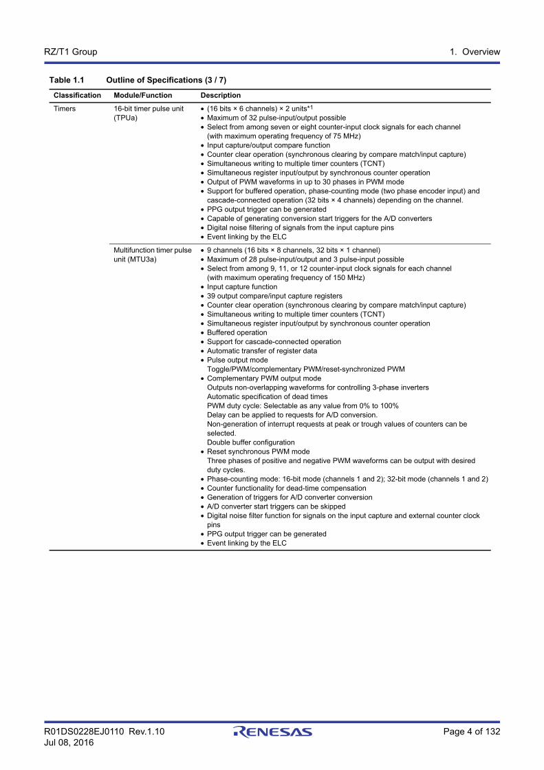
Communicationfunction
Ethernet MAC (ETHERC)
• 1 Port• IEEE802.3 is supported• 10BASE and 100BASE are supported• Full duplex and half duplex are supported• Automatic pause packet transmission function• Auto broadcast suspension function by the pause packet reception• MII/RMII interface is supported
Ethernet switch • 2-port PHY interfaces• IEEE802.3 • 10BASE, 100BASE• Full and half duplex • Hardware switching, lookup, and filtering• QoS with frame prioritization• Priority control based on VLAN Priority (IEEE802.1q), which enables priority
reassignment• Classification and priority assignment based on IPv4 DiffServ Code Point Field, IPv6
Class of Service• Queue with four priority levels • Multicasting and broadcasting• VLAN frame• IEEE1588 timer module• Cut-through and hub features• Device level ring (DLR)
EtherCAT Slave Controller (ECATC) *2
• 1 channel (2 ports) *3
• EtherCAT Slave Controller IP core (made by Beckhoff Automation GmbH) implemented
USB 2.0 HS host/function module
• 1 port• Compliance with the USB 2.0 specification• Transfer rate
High speed (480 Mbps), full speed (12 Mbps)• Communications buffer
Incorporates 1 Kbyte of RAM for host modeIncorporates 8 Kbytes of RAM for function mode
Serial communication interface with FIFO (SCIFA)
• 5 channels• Serial communications modes: Asynchronous, clock synchronous• On-chip baud rate generator allows selection of the desired bit rate• Choice of LSB-first or MSB-first transfer• Both the transmission and reception sections are equipped with 16-byte FIFO buffers,
allowing continuous transmission and reception.• Bit rate modulation
I2C bus interface (RIICa) • 2 channelsI2C bus formatSupports the multi-masterMax. transfer rate: 400 kbps
• Event linking by the ELC
CAN module (RSCAN) • 2 channels• Compliance with the ISO11898-1 specification (standard frame and extended frame)• Message buffers
Max. 64 x 2 channels of receive message buffers, which are used by all channels16 transmit message buffers per channel
• Max. transfer rate: 1 Mbps
Table 1.1 Outline of Specifications (5 / 7)
Classification Module/Function Description
R01DS0228EJ0110 Rev.1.10 Page 7 of 132Jul 08, 2016
RZ/T1 Group 1. Overview
Communicationfunction
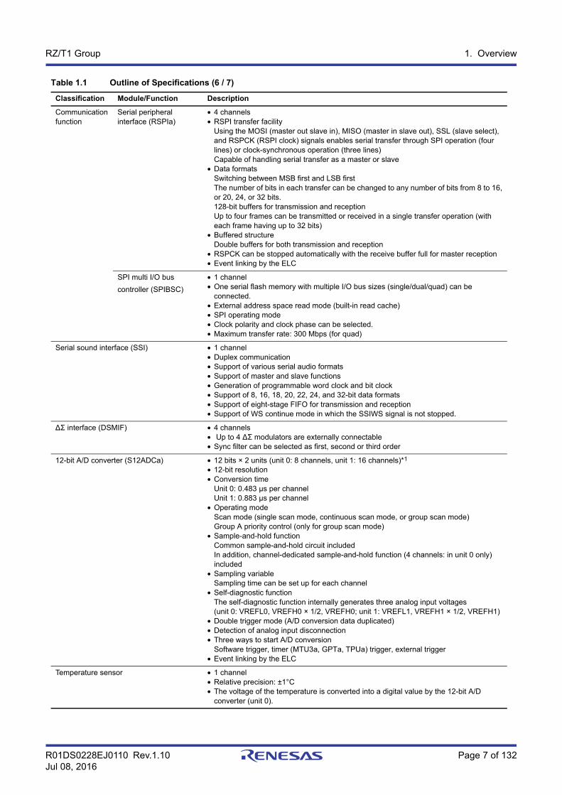
Serial peripheral interface (RSPIa)
• 4 channels• RSPI transfer facility
Using the MOSI (master out slave in), MISO (master in slave out), SSL (slave select), and RSPCK (RSPI clock) signals enables serial transfer through SPI operation (four lines) or clock-synchronous operation (three lines)Capable of handling serial transfer as a master or slave
• Data formatsSwitching between MSB first and LSB firstThe number of bits in each transfer can be changed to any number of bits from 8 to 16, or 20, 24, or 32 bits.128-bit buffers for transmission and receptionUp to four frames can be transmitted or received in a single transfer operation (with each frame having up to 32 bits)
• Buffered structureDouble buffers for both transmission and reception
• RSPCK can be stopped automatically with the receive buffer full for master reception• Event linking by the ELC
SPI multi I/O bus
controller (SPIBSC)
• 1 channel• One serial flash memory with multiple I/O bus sizes (single/dual/quad) can be
connected.• External address space read mode (built-in read cache)• SPI operating mode• Clock polarity and clock phase can be selected.• Maximum transfer rate: 300 Mbps (for quad)
Serial sound interface (SSI) • 1 channel• Duplex communication• Support of various serial audio formats• Support of master and slave functions• Generation of programmable word clock and bit clock• Support of 8, 16, 18, 20, 22, 24, and 32-bit data formats• Support of eight-stage FIFO for transmission and reception• Support of WS continue mode in which the SSIWS signal is not stopped.
∆Σ interface (DSMIF) • 4 channels• Up to 4 ∆Σ modulators are externally connectable• Sync filter can be selected as first, second or third order
12-bit A/D converter (S12ADCa) • 12 bits × 2 units (unit 0: 8 channels, unit 1: 16 channels)*1
• 12-bit resolution• Conversion time
Unit 0: 0.483 µs per channelUnit 1: 0.883 µs per channel
• Operating modeScan mode (single scan mode, continuous scan mode, or group scan mode)Group A priority control (only for group scan mode)
• Sample-and-hold functionCommon sample-and-hold circuit includedIn addition, channel-dedicated sample-and-hold function (4 channels: in unit 0 only) included
• Sampling variableSampling time can be set up for each channel
• Self-diagnostic functionThe self-diagnostic function internally generates three analog input voltages (unit 0: VREFL0, VREFH0 × 1/2, VREFH0; unit 1: VREFL1, VREFH1 × 1/2, VREFH1)
• Double trigger mode (A/D conversion data duplicated)• Detection of analog input disconnection• Three ways to start A/D conversion
Software trigger, timer (MTU3a, GPTa, TPUa) trigger, external trigger• Event linking by the ELC
Temperature sensor • 1 channel• Relative precision: ±1°C• The voltage of the temperature is converted into a digital value by the 12-bit A/D
converter (unit 0).
Table 1.1 Outline of Specifications (6 / 7)
Classification Module/Function Description
R01DS0228EJ0110 Rev.1.10 Page 8 of 132Jul 08, 2016
RZ/T1 Group 1. Overview
Note 1. One unit for 176-pin devices (only unit 0 is provided)Note 2. EtherCAT is a registered trademark of Beckhoff Automation GmbH, Germany. (optional)Note 3. Not included in 176-pin devices.Note 4. See Table 1.3, List of Products, for the products that have the secure boot mode. Details of these optional functions will only be
disclosed after completion of a binding non-disclosure agreement. For details, contact our sales representative.Note 5. This applies to the devices with the encoder interfaces. For details, contact our sales representative.
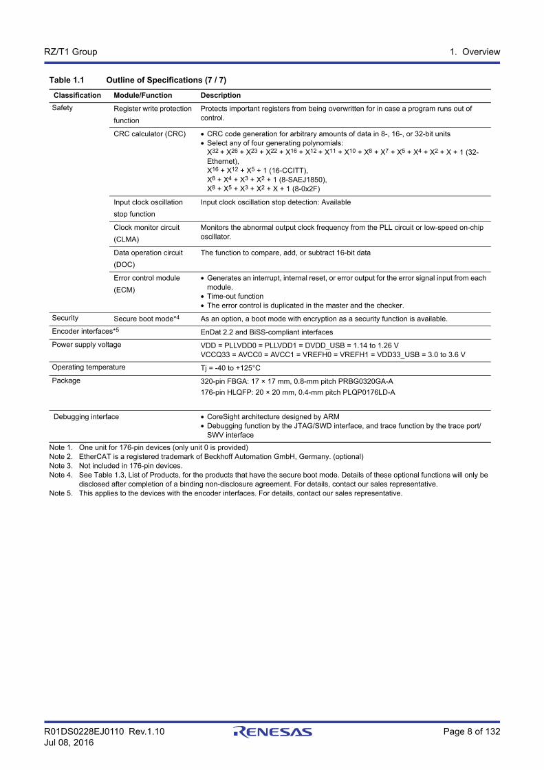
Safety Register write protection
function
Protects important registers from being overwritten for in case a program runs out of control.
CRC calculator (CRC) • CRC code generation for arbitrary amounts of data in 8-, 16-, or 32-bit units• Select any of four generating polynomials:
X32 + X26 + X23 + X22 + X16 + X12 + X11 + X10 + X8 + X7 + X5 + X4 + X2 + X + 1 (32-Ethernet), X16 + X12 + X5 + 1 (16-CCITT), X8 + X4 + X3 + X2 + 1 (8-SAEJ1850), X8 + X5 + X3 + X2 + X + 1 (8-0x2F)
Input clock oscillation
stop function
Input clock oscillation stop detection: Available
Clock monitor circuit
(CLMA)
Monitors the abnormal output clock frequency from the PLL circuit or low-speed on-chip oscillator.
Data operation circuit
(DOC)
The function to compare, add, or subtract 16-bit data
Error control module
(ECM)
• Generates an interrupt, internal reset, or error output for the error signal input from each module.
• Time-out function• The error control is duplicated in the master and the checker.
Security Secure boot mode*4 As an option, a boot mode with encryption as a security function is available.
Encoder interfaces*5 EnDat 2.2 and BiSS-compliant interfaces
Power supply voltage VDD = PLLVDD0 = PLLVDD1 = DVDD_USB = 1.14 to 1.26 VVCCQ33 = AVCC0 = AVCC1 = VREFH0 = VREFH1 = VDD33_USB = 3.0 to 3.6 V
Operating temperature Tj = -40 to +125°C
Package 320-pin FBGA: 17 × 17 mm, 0.8-mm pitch PRBG0320GA-A
176-pin HLQFP: 20 × 20 mm, 0.4-mm pitch PLQP0176LD-A
Debugging interface • CoreSight architecture designed by ARM• Debugging function by the JTAG/SWD interface, and trace function by the trace port/
SWV interface
Table 1.1 Outline of Specifications (7 / 7)
Classification Module/Function Description
R01DS0228EJ0110 Rev.1.10 Page 9 of 132Jul 08, 2016
RZ/T1 Group 1. Overview
Note 1. See Table 1.3, List of Products for the products that have the secure boot mode. Details of these optional functions will only be disclosed after completion of a binding non-disclosure agreement. For details, contact our sales representative.
Note 2. For details, contact our sales representative.
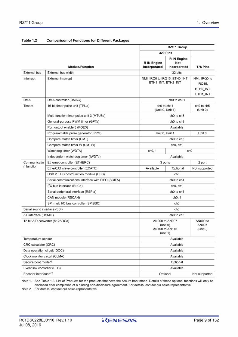
Table 1.2 Comparison of Functions for Different Packages
Module/Function
RZ/T1 Group
320 Pins
176 PinsR-IN EngineIncorporated
R-IN EngineNot-
Incorporated
External bus External bus width 32 bits
Interrupt External interrupt NMI, IRQ0 to IRQ15, ETH0_INT, ETH1_INT, ETH2_INT
NMI, IRQ0 to
IRQ15,
ETH0_INT,
ETH1_INT
DMA DMA controller (DMAC) ch0 to ch31
Timers 16-bit timer pulse unit (TPUa) ch0 to ch11(Unit 0, Unit 1)
ch0 to ch5(Unit 0)
Multi-function timer pulse unit 3 (MTU3a) ch0 to ch8
General-purpose PWM timer (GPTa) ch0 to ch3
Port output enable 3 (POE3) Available
Programmable pulse generator (PPG) Unit 0, Unit 1 Unit 0
Compare match timer (CMT) ch0 to ch5
Compare match timer W (CMTW) ch0, ch1
Watchdog timer (WDTA) ch0, 1 ch0
Independent watchdog timer (IWDTa) Available
Communication function
Ethernet controller (ETHERC) 3 ports 2 port
EtherCAT slave controller (ECATC) Available Optional Not supported
USB 2.0 HS host/function module (USB) ch0
Serial communications interface with FIFO (SCIFA) ch0 to ch4
I2C bus interface (RIICa) ch0, ch1
Serial peripheral interface (RSPIa) ch0 to ch3
CAN module (RSCAN) ch0, 1
SPI multi I/O bus controller (SPIBSC) ch0
Serial sound interface (SSI) ch0
∆Σ interface (DSMIF) ch0 to ch3
12-bit A/D converter (S12ADCa) AN000 to AN007(unit 0)
AN100 to AN115(unit 1)
AN000 to AN007(unit 0)
Temperature sensor Available
CRC calculator (CRC) Available
Data operation circuit (DOC) Available
Clock monitor circuit (CLMA) Available
Secure boot mode*1 Optional
Event link controller (ELC) Available
Encoder interfaces*2 Optional Not supported
R01DS0228EJ0110 Rev.1.10 Page 10 of 132Jul 08, 2016
RZ/T1 Group 1. Overview
1.2 List of Products
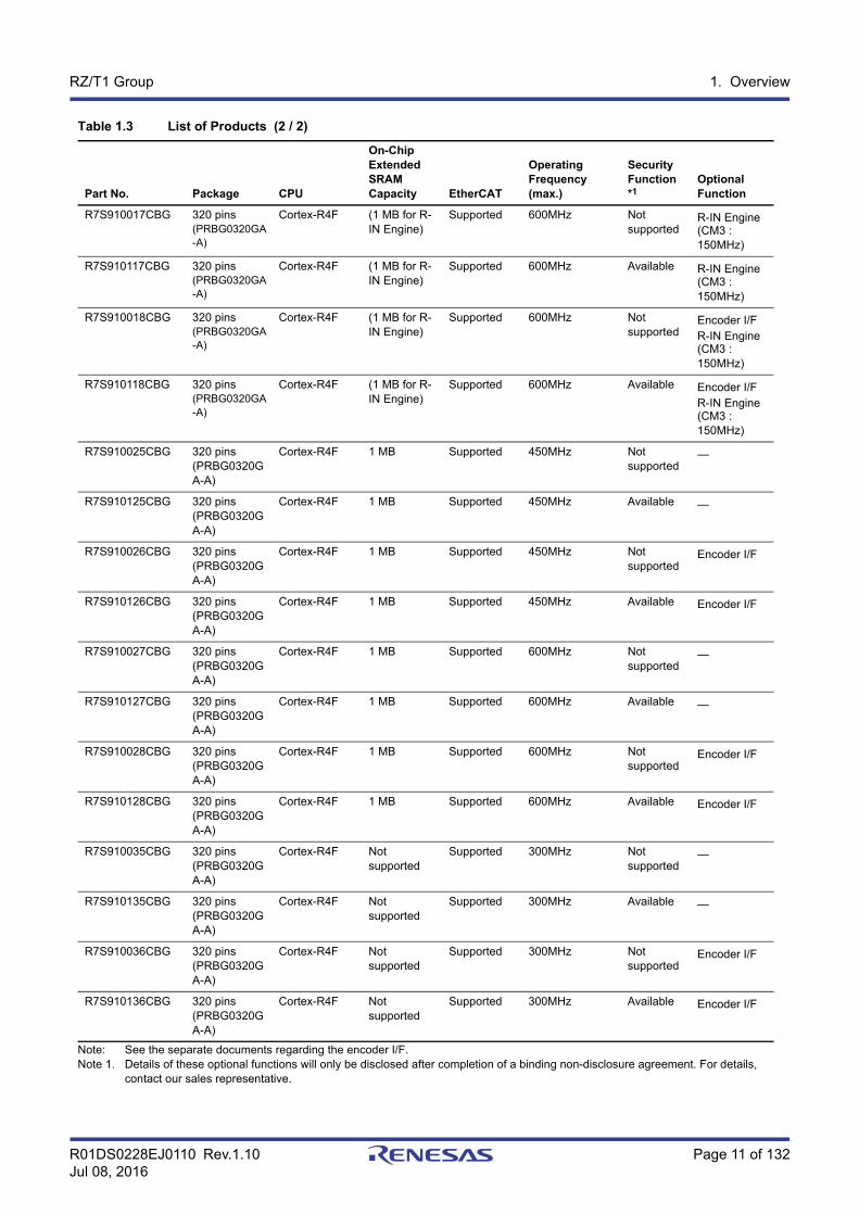
Table 1.3 is a list of products.
Table 1.3 List of Products (1 / 2)
Part No. Package CPU
On-Chip Extended SRAM Capacity EtherCAT
Operating Frequency (max.)
Security Function*1
Optional Function
R7S910001CFP 176 pins(PLQP0176LD-A)
Cortex-R4F Not supported
Not supported
450MHz Not supported
—
R7S910101CFP 176 pins(PLQP0176LD-A)
Cortex-R4F Not supported
Not supported
450MHz Available —
R7S910002CBG 320 pins(PRBG0320GA-A)
Cortex-R4F Not supported
Not supported
450MHz Not supported
—
R7S910102CBG 320 pins(PRBG0320GA-A)
Cortex-R4F Not supported
Not supported
450MHz Available —
R7S910006CBG 320 pins(PRBG0320GA-A)
Cortex-R4F 1 Mbyte Not supported
450MHz Not supported
—
R7S910106CBG 320 pins(PRBG0320GA-A)
Cortex-R4F 1 Mbyte Not supported
450MHz Available —
R7S910007CBG 320 pins(PRBG0320GA-A)
Cortex-R4F 1 Mbyte Not supported
600MHz Not supported
—
R7S910107CBG 320 pins(PRBG0320GA-A)
Cortex-R4F 1 Mbyte Not supported
600MHz Available —
R7S910011CBG 320 pins(PRBG0320GA-A)
Cortex-R4F Not supported
Not supported
450MHz Not supported
Encoder I/F
R7S910111CBG 320 pins(PRBG0320GA-A)
Cortex-R4F Not supported
Not supported
450MHz Available Encoder I/F
R7S910013CBG 320 pins(PRBG0320GA-A)
Cortex-R4F 1 Mbyte Not supported
600MHz Not supported
Encoder I/F
R7S910113CBG 320 pins(PRBG0320GA-A)
Cortex-R4F 1 Mbyte Not supported
600MHz Available Encoder I/F
R7S910015CBG 320 pins(PRBG0320GA-A)
Cortex-R4F (1 MB for R-IN Engine)
Supported 450MHz Not supported
R-IN Engine(CM3 : 150MHz)
R7S910115CBG 320 pins(PRBG0320GA-A)
Cortex-R4F (1 MB for R-IN Engine)
Supported 450MHz Available R-IN Engine(CM3 : 150MHz)
R7S910016CBG 320 pins(PRBG0320GA-A)
Cortex-R4F (1 MB for R-IN Engine)
Supported 450MHz Not supported
Encoder I/FR-IN Engine(CM3 : 150MHz)
R7S910116CBG 320 pins(PRBG0320GA-A)
Cortex-R4F (1 MB for R-IN Engine)
Supported 450MHz Available Encoder I/FR-IN Engine(CM3 : 150MHz)
R01DS0228EJ0110 Rev.1.10 Page 11 of 132Jul 08, 2016
RZ/T1 Group 1. Overview
Note: See the separate documents regarding the encoder I/F.Note 1. Details of these optional functions will only be disclosed after completion of a binding non-disclosure agreement. For details,
contact our sales representative.
R7S910017CBG 320 pins(PRBG0320GA-A)
Cortex-R4F (1 MB for R-IN Engine)
Supported 600MHz Not supported
R-IN Engine(CM3 : 150MHz)
R7S910117CBG 320 pins(PRBG0320GA-A)
Cortex-R4F (1 MB for R-IN Engine)
Supported 600MHz Available R-IN Engine(CM3 : 150MHz)
R7S910018CBG 320 pins(PRBG0320GA-A)
Cortex-R4F (1 MB for R-IN Engine)
Supported 600MHz Not supported
Encoder I/FR-IN Engine(CM3 : 150MHz)
R7S910118CBG 320 pins(PRBG0320GA-A)
Cortex-R4F (1 MB for R-IN Engine)
Supported 600MHz Available Encoder I/FR-IN Engine(CM3 : 150MHz)
R7S910025CBG 320 pins(PRBG0320GA-A)
Cortex-R4F 1 MB Supported 450MHz Not supported
—
R7S910125CBG 320 pins(PRBG0320GA-A)
Cortex-R4F 1 MB Supported 450MHz Available —
R7S910026CBG 320 pins(PRBG0320GA-A)
Cortex-R4F 1 MB Supported 450MHz Not supported
Encoder I/F
R7S910126CBG 320 pins(PRBG0320GA-A)
Cortex-R4F 1 MB Supported 450MHz Available Encoder I/F
R7S910027CBG 320 pins(PRBG0320GA-A)
Cortex-R4F 1 MB Supported 600MHz Not supported
—
R7S910127CBG 320 pins(PRBG0320GA-A)
Cortex-R4F 1 MB Supported 600MHz Available —
R7S910028CBG 320 pins(PRBG0320GA-A)
Cortex-R4F 1 MB Supported 600MHz Not supported
Encoder I/F
R7S910128CBG 320 pins(PRBG0320GA-A)
Cortex-R4F 1 MB Supported 600MHz Available Encoder I/F
R7S910035CBG 320 pins(PRBG0320GA-A)
Cortex-R4F Not supported
Supported 300MHz Not supported
—
R7S910135CBG 320 pins(PRBG0320GA-A)
Cortex-R4F Not supported
Supported 300MHz Available —
R7S910036CBG 320 pins(PRBG0320GA-A)
Cortex-R4F Not supported
Supported 300MHz Not supported
Encoder I/F
R7S910136CBG 320 pins(PRBG0320GA-A)
Cortex-R4F Not supported
Supported 300MHz Available Encoder I/F
Table 1.3 List of Products (2 / 2)
Part No. Package CPU
On-Chip Extended SRAM Capacity EtherCAT
Operating Frequency (max.)
Security Function*1
Optional Function
R01DS0228EJ0110 Rev.1.10 Page 12 of 132Jul 08, 2016
RZ/T1 Group 1. Overview
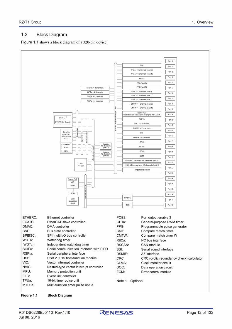
1.3 Block Diagram
Figure 1.1 shows a block diagram of a 320-pin device.
ETHERC: Ethernet controllerECATC: EtherCAT slave controllerDMAC: DMA controllerBSC: Bus state controllerSPIBSC: SPI multi I/O bus controllerWDTA: Watchdog timerIWDTa: Independent watchdog timerSCIFA: Serial communication interface with FIFORSPIa: Serial peripheral interfaceUSB: USB 2.0 HS host/function moduleVIC: Vector interrupt controllerNVIC: Nested-type vector interrupt controllerMPU: Memory protection unitELC: Event link controllerTPUa: 16-bit timer pulse unitMTU3a: Multi-function timer pulse unit 3
POE3: Port output enable 3GPTa: General-purpose PWM timerPPG: Programmable pulse generatorCMT: Compare match timerCMTW: Compare match timer W
RIICa: I2C bus interfaceRSCAN: CAN moduleSSI: Serial sound interfaceDSMIF: ∆Σ interfaceCRC: CRC (cyclic redundancy check) calculatorCLMA: Clock monitor circuitDOC: Data operation circuitECM: Error control module
Note 1. Optional
Figure 1.1 Block Diagram
CMT × 2 channels (unit 1)
CMTW × 1 channel (unit 1)
CMTW × 1 channel (unit 0)
CMT × 2 channels (unit 2)
BSC
Inte
rna
l mai
n b
us 1
Clock generation
circuit
Cortex-R4F
Port 0
Port 1
Port 2
Port 3
Port 4
Port 5
Port 6
Port 7
Port 8
Port 9
Port A
Port B
Port C
12-bit A/D converter × 16 channels (unit 1)
MTU3a × 9 channels
WDTA×1chProducts incorporating an R-IN engine: WDTA×2ch
RIIC × 2 channels
CRC
IWDTa
USB × 1 port
RSCAN × 2 channels
POE3
TPUa × 6 channels (unit 0)
CMT × 2 channels (unit 0)
PPG (unit 1)
PPG (unit 0)
RSPIa × 4 channels
Inte
rna
l mai
n b
us 2
DMAC ×16 channels
(unit 0)
Temperature sensor
GPTa × 4 channels
Port D
Port E
Port F
Port G
Port H
Port J
Port K
Port L
MPU
SCIFA × 5 channels
ETHERC × 3 ports
ECATC *1
DOC
CLMA
On-chip extended
SRAM with ECC
Port P
Port M
Port N
Port T
Port R
Port S
VIC
TCM
Inte
rna
l per
iphe
ral b
use
s 1
to 7
Cortex-M3*1
MPU
NVIC
DMAC × 16 channels
(unit 1)
ELC
TPUa × 6 channels (unit 1)
SSI
DSMIF × 4 channels
ECM
12-bit A/D converter × 8 channels (unit 0)
SPIBSC
Op
eran
d b
us
Sys
tem
bus
Inst
ruct
ion
bus
Port U
R01DS0228EJ0110 Rev.1.10 Page 13 of 132Jul 08, 2016
RZ/T1 Group 1. Overview
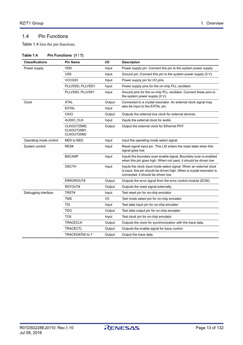
1.4 Pin Functions
Table 1.4 lists the pin functions.
Table 1.4 Pin Functions (1 / 7)
Classifications Pin Name I/O Description
Power supply VDD Input Power supply pin. Connect this pin to the system power supply.
VSS Input Ground pin. Connect this pin to the system power supply (0 V).
VCCQ33 Input Power supply pin for I/O pins
PLLVDD0, PLLVDD1 Input Power supply pins for the on-chip PLL oscillator
PLLVSS0, PLLVSS1 Input Ground pins for the on-chip PLL oscillator. Connect these pins to the system power supply (0 V).
Clock XTAL Output Connected to a crystal resonator. An external clock signal may also be input to the EXTAL pin.
EXTAL Input
CKIO Output Outputs the external bus clock for external devices.
AUDIO_CLK Input Inputs the external clock for audio.
CLKOUT25M0,CLKOUT25M1,CLKOUT25M2
Output Output the external clock for Ethernet PHY.
Operating mode control MD0 to MD2 Input Input the operating mode select signal.
System control RES# Input Reset signal input pin. This LSI enters the reset state when this signal goes low.
BSCANP Input Inputs the boundary scan enable signal. Boundary scan is enabled when this pin goes high. When not used, it should be driven low.
OSCTH Input Inputs the clock input mode select signal. When an external clock is input, this pin should be driven high. When a crystal resonator is connected, it should be driven low.
ERROROUT# Output Outputs the error signal from the error control module (ECM).
RSTOUT# Output Outputs the reset signal externally.
Debugging interface TRST# Input Test reset pin for on-chip emulator
TMS I/O Test mode select pin for on-chip emulator
TDI Input Test data input pin for on-chip emulator
TDO Output Test data output pin for on-chip emulator
TCK Input Test clock pin for on-chip emulator
TRACECLK Output Outputs the clock for synchronization with the trace data.
TRACECTL Output Outputs the enable signal for trace control.
TRACEDATA0 to 7 Output Output the trace data.
R01DS0228EJ0110 Rev.1.10 Page 14 of 132Jul 08, 2016
RZ/T1 Group 1. Overview
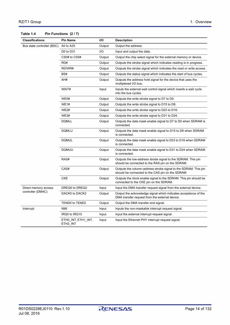
Bus state controller (BSC) A0 to A25 Output Output the address.
D0 to D31 I/O Input and output the data.
CS0# to CS5# Output Output the chip select signal for the external memory or device.
RD# Output Outputs the strobe signal which indicates reading is in progress.
RD/WR# Output Outputs the strobe signal which indicates the read or write access.
BS# Output Outputs the status signal which indicates the start of bus cycles.
AH# Output Outputs the address hold signal for the device that uses the multiplexed I/O bus.
WAIT# Input Inputs the external wait control signal which inserts a wait cycle into the bus cycles.
WE0# Output Outputs the write strobe signal to D7 to D0.
WE1# Output Outputs the write strobe signal to D15 to D8.
WE2# Output Outputs the write strobe signal to D23 to D16.
WE3# Output Outputs the write strobe signal to D31 to D24.
DQMLL Output Outputs the data mask enable signal to D7 to D0 when SDRAM is connected.
DQMLU Output Outputs the data mask enable signal to D15 to D8 when SDRAM is connected.
DQMUL Output Outputs the data mask enable signal to D23 to D16 when SDRAM is connected.
DQMUU Output Outputs the data mask enable signal to D31 to D24 when SDRAM is connected.
RAS# Output Outputs the low-address strobe signal to the SDRAM. This pin should be connected to the RAS pin on the SDRAM.
CAS# Output Outputs the column-address strobe signal to the SDRAM. This pin should be connected to the CAS pin on the SDRAM.
CKE Output Outputs the clock enable signal to the SDRAM. This pin should be connected to the CKE pin on the SDRAM.
Direct memory access controller (DMAC)
DREQ0 to DREQ2 Input Input the DMA transfer request signal from the external device.
DACK0 to DACK2 Output Output the acknowledge signal which indicates acceptance of the DMA transfer request from the external device.
TEND0 to TEND2 Output Output the DMA transfer end signal.
Interrupt NMI Input Inputs the non-maskable interrupt request signal.
IRQ0 to IRQ15 Input Input the external interrupt request signal.
ETH0_INT, ETH1_INT, ETH2_INT
Input Input the Ethernet PHY interrupt request signal.
Table 1.4 Pin Functions (2 / 7)
Classifications Pin Name I/O Description

R01DS0228EJ0110 Rev.1.10 Page 15 of 132Jul 08, 2016
RZ/T1 Group 1. Overview
Multi-function timer pulse unit 3 (MTU3a)
MTIOC0A, MTIOC0BMTIOC0C, MTIOC0D
I/O TGRA0 to TGRD0 input capture input/output compare output/PWM output pins
MTIOC1A, MTIOC1B I/O TGRA1 and TGRB1 input capture input/output compare output/PWM output pins
MTIOC2A, MTIOC2B I/O TGRA2 and TGRB2 input capture input/output compare output/PWM output pins
MTIOC3A, MTIOC3BMTIOC3C, MTIOC3D
I/O TGRA3 to TGRD3 input capture input/output compare output/PWM output pins
MTIOC4A, MTIOC4BMTIOC4C, MTIOC4D
I/O TGRA4 to TGRD4 input capture input/output compare output/PWM output pins
MTIC5U, MTIC5VMTIC5W
Input TGRU5, TGRV5, and TGRW5 input capture input/dead time compensation input pins
MTIOC6A, MTIOC6BMTIOC6C, MTIOC6D
I/O TGRA6 to TGRD6 input capture input/output compare output/PWM output pins
MTIOC7A, MTIOC7BMTIOC7C, MTIOC7D
I/O TGRA7 to TGRD7 input capture input/output compare output/PWM output pins
MTIOC8A, MTIOC8BMTIOC8C, MTIOC8D
I/O TGRA8 to TGRD8 input capture input/output compare output/PWM output pins
MTCLKA, MTCLKBMTCLKC, MTCLKD
Input External clock input pins for MTU3a
Port output enable 3 (POE3)
POE0#, POE4#POE8#, POE10#
Input Input the request signal to place the MTU3a or GPTa in the high impedance state.
General-purpose PWM timer (GPTa)
GTIOC0A, GTIOC0B I/O GPT0.GTGRA and GPT0.GTGRB input capture input/output compare output/PWM output pins
GTIOC1A, GTIOC1B I/O GPT1.GTGRA and GPT1.GTGRB input capture input/output compare output/PWM output pins
GTIOC2A, GTIOC2B I/O GPT2.GTGRA and GPT2.GTGRB input capture input/output compare output/PWM output pins
GTIOC3A, GTIOC3B I/O GPT3.GTGRA and GPT3.GTGRB input capture input/output compare output/PWM output pins
GTETRG Input External trigger input pin for GPT0 to GPT3
Table 1.4 Pin Functions (3 / 7)
Classifications Pin Name I/O Description
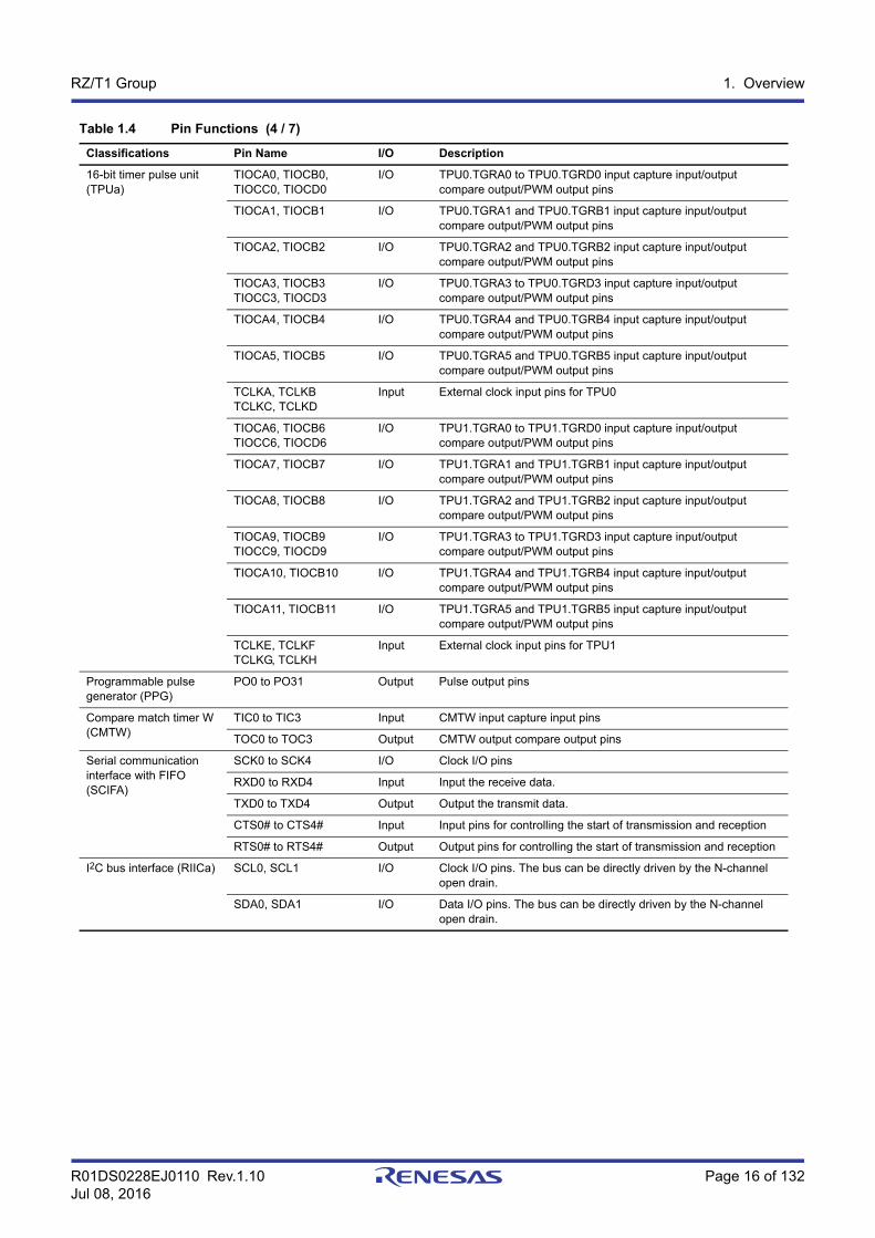
R01DS0228EJ0110 Rev.1.10 Page 16 of 132Jul 08, 2016
RZ/T1 Group 1. Overview
16-bit timer pulse unit (TPUa)
TIOCA0, TIOCB0,TIOCC0, TIOCD0
I/O TPU0.TGRA0 to TPU0.TGRD0 input capture input/output compare output/PWM output pins
TIOCA1, TIOCB1 I/O TPU0.TGRA1 and TPU0.TGRB1 input capture input/output compare output/PWM output pins
TIOCA2, TIOCB2 I/O TPU0.TGRA2 and TPU0.TGRB2 input capture input/output compare output/PWM output pins
TIOCA3, TIOCB3TIOCC3, TIOCD3
I/O TPU0.TGRA3 to TPU0.TGRD3 input capture input/output compare output/PWM output pins
TIOCA4, TIOCB4 I/O TPU0.TGRA4 and TPU0.TGRB4 input capture input/output compare output/PWM output pins
TIOCA5, TIOCB5 I/O TPU0.TGRA5 and TPU0.TGRB5 input capture input/output compare output/PWM output pins
TCLKA, TCLKBTCLKC, TCLKD
Input External clock input pins for TPU0
TIOCA6, TIOCB6TIOCC6, TIOCD6
I/O TPU1.TGRA0 to TPU1.TGRD0 input capture input/output compare output/PWM output pins
TIOCA7, TIOCB7 I/O TPU1.TGRA1 and TPU1.TGRB1 input capture input/output compare output/PWM output pins
TIOCA8, TIOCB8 I/O TPU1.TGRA2 and TPU1.TGRB2 input capture input/output compare output/PWM output pins
TIOCA9, TIOCB9TIOCC9, TIOCD9
I/O TPU1.TGRA3 to TPU1.TGRD3 input capture input/output compare output/PWM output pins
TIOCA10, TIOCB10 I/O TPU1.TGRA4 and TPU1.TGRB4 input capture input/output compare output/PWM output pins
TIOCA11, TIOCB11 I/O TPU1.TGRA5 and TPU1.TGRB5 input capture input/output compare output/PWM output pins
TCLKE, TCLKFTCLKG, TCLKH
Input External clock input pins for TPU1
Programmable pulsegenerator (PPG)
PO0 to PO31 Output Pulse output pins
Compare match timer W (CMTW)
TIC0 to TIC3 Input CMTW input capture input pins
TOC0 to TOC3 Output CMTW output compare output pins
Serial communication interface with FIFO (SCIFA)
SCK0 to SCK4 I/O Clock I/O pins
RXD0 to RXD4 Input Input the receive data.
TXD0 to TXD4 Output Output the transmit data.
CTS0# to CTS4# Input Input pins for controlling the start of transmission and reception
RTS0# to RTS4# Output Output pins for controlling the start of transmission and reception
I2C bus interface (RIICa) SCL0, SCL1 I/O Clock I/O pins. The bus can be directly driven by the N-channel open drain.
SDA0, SDA1 I/O Data I/O pins. The bus can be directly driven by the N-channel open drain.
Table 1.4 Pin Functions (4 / 7)
Classifications Pin Name I/O Description
R01DS0228EJ0110 Rev.1.10 Page 17 of 132Jul 08, 2016
RZ/T1 Group 1. Overview
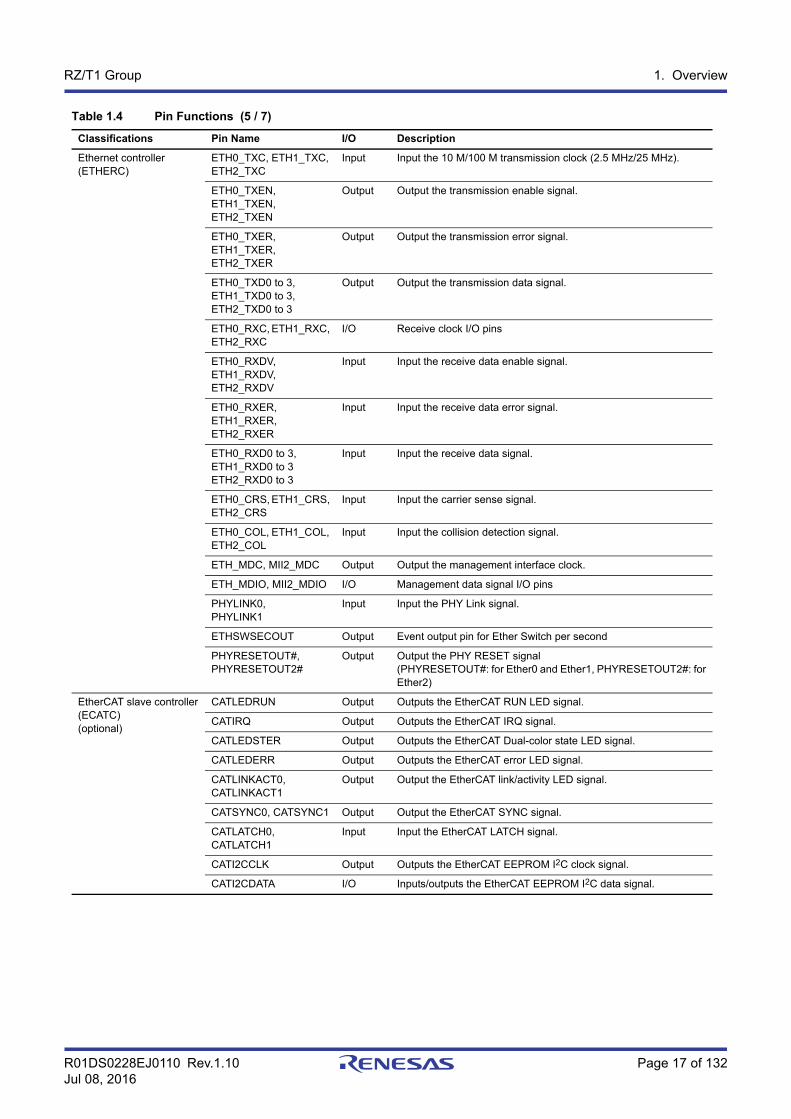
Ethernet controller (ETHERC)
ETH0_TXC, ETH1_TXC, ETH2_TXC
Input Input the 10 M/100 M transmission clock (2.5 MHz/25 MHz).
ETH0_TXEN, ETH1_TXEN, ETH2_TXEN
Output Output the transmission enable signal.
ETH0_TXER, ETH1_TXER, ETH2_TXER
Output Output the transmission error signal.
ETH0_TXD0 to 3, ETH1_TXD0 to 3, ETH2_TXD0 to 3
Output Output the transmission data signal.
ETH0_RXC, ETH1_RXC, ETH2_RXC
I/O Receive clock I/O pins
ETH0_RXDV, ETH1_RXDV, ETH2_RXDV
Input Input the receive data enable signal.
ETH0_RXER, ETH1_RXER, ETH2_RXER
Input Input the receive data error signal.
ETH0_RXD0 to 3, ETH1_RXD0 to 3ETH2_RXD0 to 3
Input Input the receive data signal.
ETH0_CRS, ETH1_CRS, ETH2_CRS
Input Input the carrier sense signal.
ETH0_COL, ETH1_COL, ETH2_COL
Input Input the collision detection signal.
ETH_MDC, MII2_MDC Output Output the management interface clock.
ETH_MDIO, MII2_MDIO I/O Management data signal I/O pins
PHYLINK0,PHYLINK1
Input Input the PHY Link signal.
ETHSWSECOUT Output Event output pin for Ether Switch per second
PHYRESETOUT#, PHYRESETOUT2#
Output Output the PHY RESET signal(PHYRESETOUT#: for Ether0 and Ether1, PHYRESETOUT2#: for Ether2)
EtherCAT slave controller (ECATC)(optional)
CATLEDRUN Output Outputs the EtherCAT RUN LED signal.
CATIRQ Output Outputs the EtherCAT IRQ signal.
CATLEDSTER Output Outputs the EtherCAT Dual-color state LED signal.
CATLEDERR Output Outputs the EtherCAT error LED signal.
CATLINKACT0, CATLINKACT1
Output Output the EtherCAT link/activity LED signal.
CATSYNC0, CATSYNC1 Output Output the EtherCAT SYNC signal.
CATLATCH0, CATLATCH1
Input Input the EtherCAT LATCH signal.
CATI2CCLK Output Outputs the EtherCAT EEPROM I2C clock signal.
CATI2CDATA I/O Inputs/outputs the EtherCAT EEPROM I2C data signal.
Table 1.4 Pin Functions (5 / 7)
Classifications Pin Name I/O Description
R01DS0228EJ0110 Rev.1.10 Page 18 of 132Jul 08, 2016
RZ/T1 Group 1. Overview
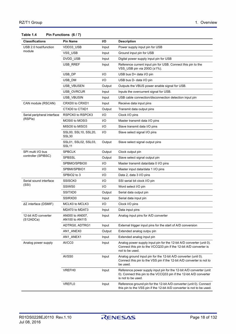
USB 2.0 host/function module
VDD33_USB Input Power supply input pin for USB
VSS_USB Input Ground input pin for USB
DVDD_USB Input Digital power supply input pin for USB
USB_RREF Input Reference current input pin for USB. Connect this pin to the VSS_USB pin via 200Ω (±1%).
USB_DP I/O USB bus D+ data I/O pin
USB_DM I/O USB bus D- data I/O pin
USB_VBUSEN Output Outputs the VBUS power enable signal for USB.
USB_OVRCUR Input Inputs the overcurrent signal for USB.
USB_VBUSIN Input USB cable connection/disconnection detection input pin
CAN module (RSCAN) CRXD0 to CRXD1 Input Receive data input pins
CTXD0 to CTXD1 Output Transmit data output pins
Serial peripheral interface (RSPIa)
RSPCK0 to RSPCK3 I/O Clock I/O pins
MOSI0 to MOSI3 I/O Master transmit data I/O pins
MISO0 to MISO3 I/O Slave transmit data I/O pins
SSL00, SSL10, SSL20, SSL30
I/O Slave select signal I/O pins
SSL01, SSL02, SSL03, SSL11
Output Slave select signal output pins
SPI multi I/O bus controller (SPIBSC)
SPBCLK Output Clock output pin
SPBSSL Output Slave select signal output pin
SPBMO/SPBIO0 I/O Master transmit data/data 0 I/O pins
SPBMI/SPBIO1 I/O Master input data/data 1 I/O pins
SPBIO2 to 3 I/O Data 2, data 3 I/O pins
Serial sound interface (SSI)
SSISCK0 I/O SSI serial bit clock I/O pin
SSIWS0 I/O Word select I/O pin
SSITXD0 Output Serial data output pin
SSIRXD0 Input Serial data input pin
∆Σ interface (DSMIF) MCLK0 to MCLK3 I/O Clock I/O pins
MDAT0 to MDAT3 Input Data input pins
12-bit A/D converter (S12ADCa)
AN000 to AN007, AN100 to AN115
Input Analog input pins for A/D converter
ADTRG0, ADTRG1 Input External trigger input pins for the start of A/D conversion
AN1_ANEX0 Output Extended analog outpu pin
AN1_ANEX1 Input Extended analog input pin
Analog power supply AVCC0 Input Analog power supply input pin for the 12-bit A/D converter (unit 0). Connect this pin to the VCCQ33 pin if the 12-bit A/D converter is not to be used.
AVSS0 Input Analog ground input pin for the 12-bit A/D converter (unit 0). Connect this pin to the VSS pin if the 12-bit A/D converter is not to be used.
VREFH0 Input Reference power supply input pin for the 12-bit A/D converter (unit 0). Connect this pin to the VCCQ33 pin if the 12-bit A/D converter is not to be used.
VREFL0 Input Reference ground pin for the 12-bit A/D converter (unit 0). Connect this pin to the VSS pin if the 12-bit A/D converter is not to be used.
Table 1.4 Pin Functions (6 / 7)
Classifications Pin Name I/O Description
R01DS0228EJ0110 Rev.1.10 Page 19 of 132Jul 08, 2016
RZ/T1 Group 1. Overview
Note 1. Only in products with the encoder interfaces.
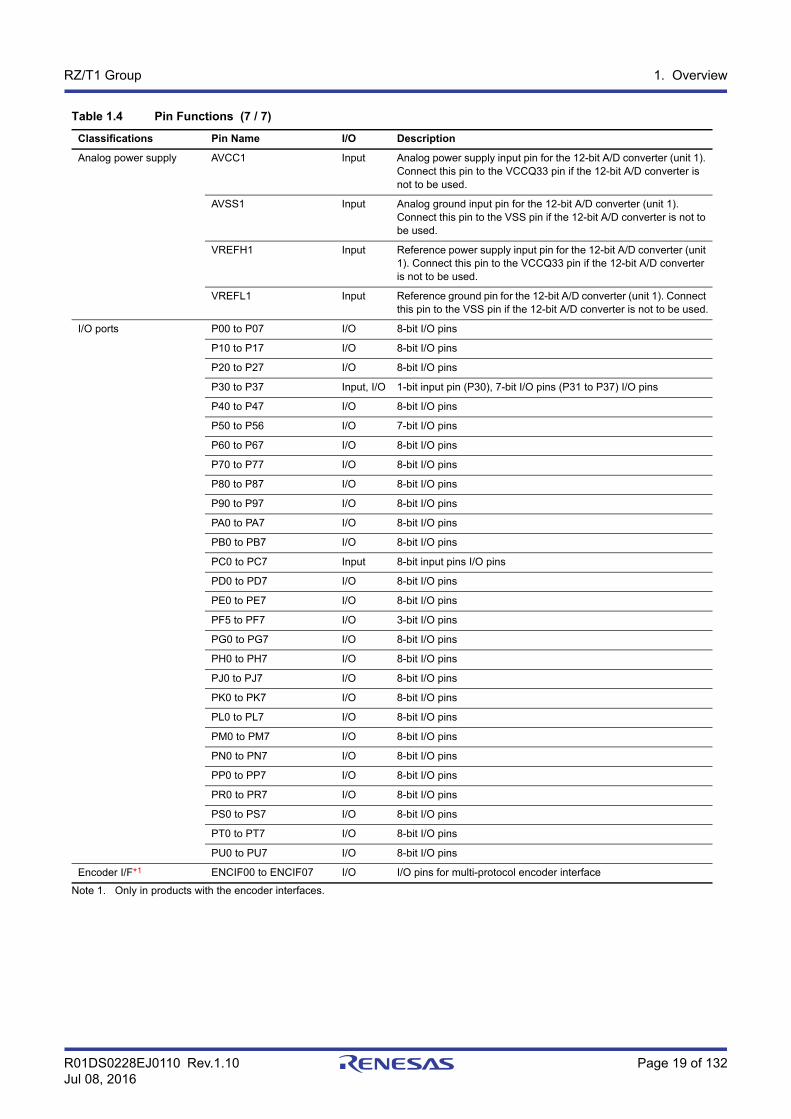
Analog power supply AVCC1 Input Analog power supply input pin for the 12-bit A/D converter (unit 1). Connect this pin to the VCCQ33 pin if the 12-bit A/D converter is not to be used.
AVSS1 Input Analog ground input pin for the 12-bit A/D converter (unit 1). Connect this pin to the VSS pin if the 12-bit A/D converter is not to be used.
VREFH1 Input Reference power supply input pin for the 12-bit A/D converter (unit 1). Connect this pin to the VCCQ33 pin if the 12-bit A/D converter is not to be used.
VREFL1 Input Reference ground pin for the 12-bit A/D converter (unit 1). Connect this pin to the VSS pin if the 12-bit A/D converter is not to be used.
I/O ports P00 to P07 I/O 8-bit I/O pins
P10 to P17 I/O 8-bit I/O pins
P20 to P27 I/O 8-bit I/O pins
P30 to P37 Input, I/O 1-bit input pin (P30), 7-bit I/O pins (P31 to P37) I/O pins
P40 to P47 I/O 8-bit I/O pins
P50 to P56 I/O 7-bit I/O pins
P60 to P67 I/O 8-bit I/O pins
P70 to P77 I/O 8-bit I/O pins
P80 to P87 I/O 8-bit I/O pins
P90 to P97 I/O 8-bit I/O pins
PA0 to PA7 I/O 8-bit I/O pins
PB0 to PB7 I/O 8-bit I/O pins
PC0 to PC7 Input 8-bit input pins I/O pins
PD0 to PD7 I/O 8-bit I/O pins
PE0 to PE7 I/O 8-bit I/O pins
PF5 to PF7 I/O 3-bit I/O pins
PG0 to PG7 I/O 8-bit I/O pins
PH0 to PH7 I/O 8-bit I/O pins
PJ0 to PJ7 I/O 8-bit I/O pins
PK0 to PK7 I/O 8-bit I/O pins
PL0 to PL7 I/O 8-bit I/O pins
PM0 to PM7 I/O 8-bit I/O pins
PN0 to PN7 I/O 8-bit I/O pins
PP0 to PP7 I/O 8-bit I/O pins
PR0 to PR7 I/O 8-bit I/O pins
PS0 to PS7 I/O 8-bit I/O pins
PT0 to PT7 I/O 8-bit I/O pins
PU0 to PU7 I/O 8-bit I/O pins
Encoder I/F*1 ENCIF00 to ENCIF07 I/O I/O pins for multi-protocol encoder interface
Table 1.4 Pin Functions (7 / 7)
Classifications Pin Name I/O Description
R01DS0228EJ0110 Rev.1.10 Page 20 of 132Jul 08, 2016
RZ/T1 Group 1. Overview
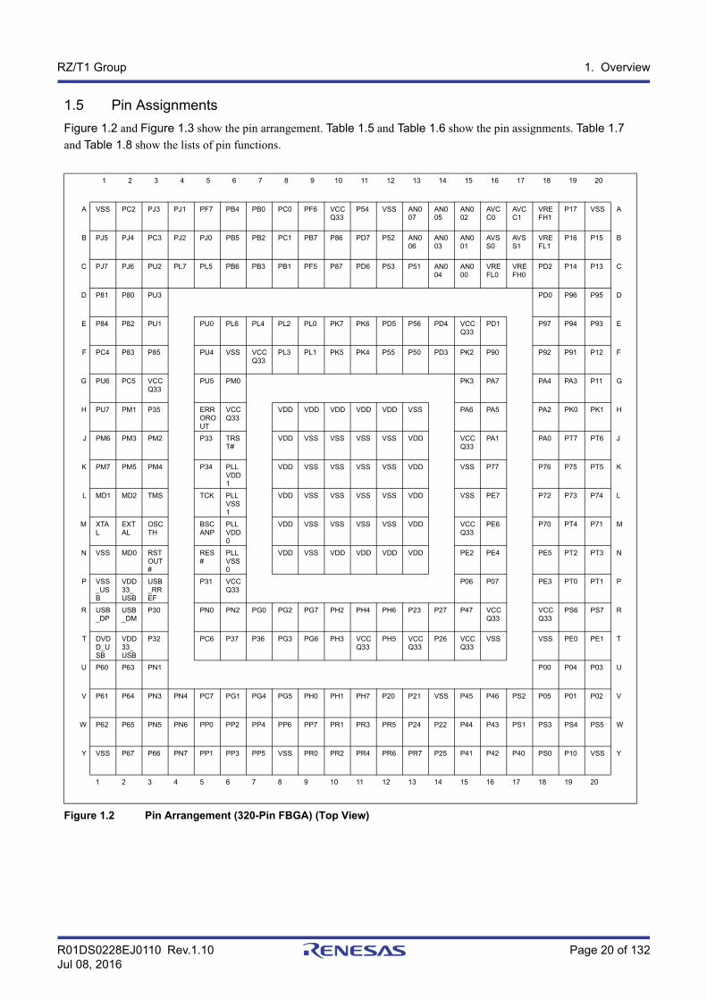
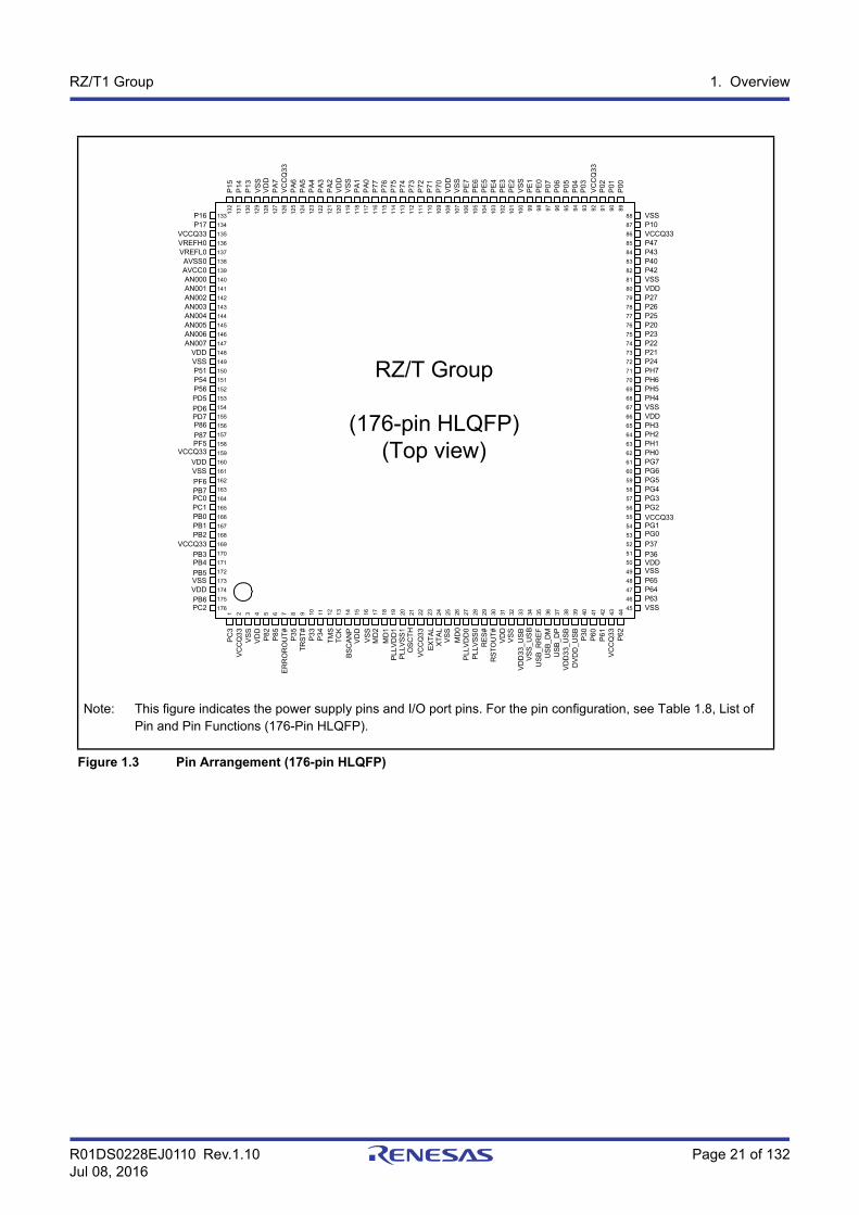
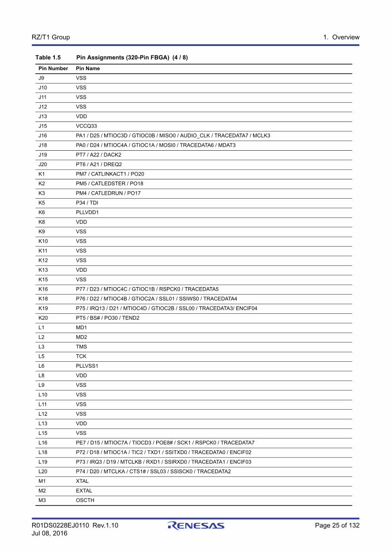
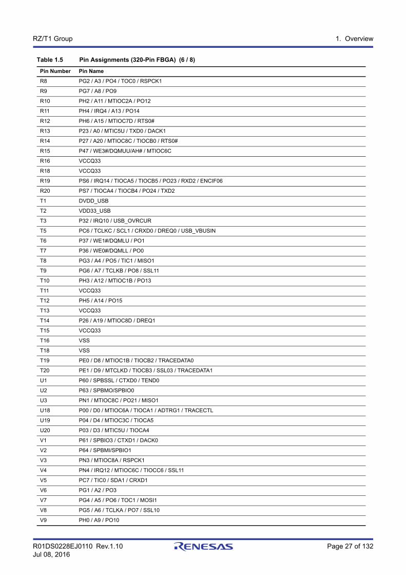
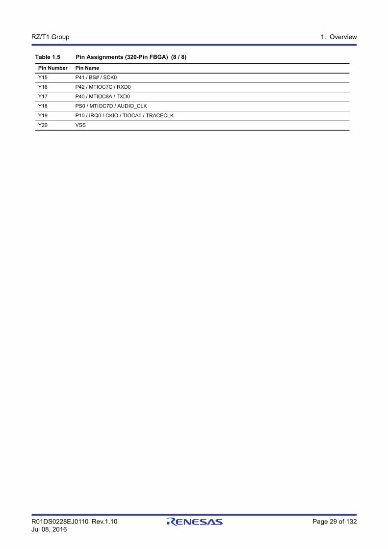
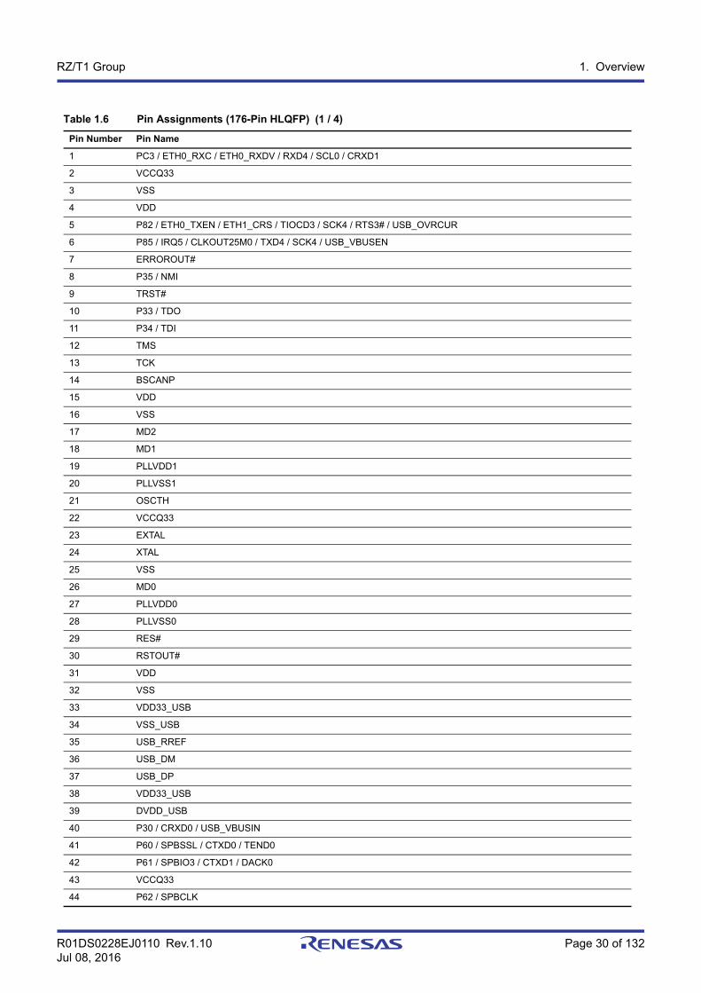
1.5 Pin Assignments
Figure 1.2 and Figure 1.3 show the pin arrangement. Table 1.5 and Table 1.6 show the pin assignments. Table 1.7
and Table 1.8 show the lists of pin functions.
Figure 1.2 Pin Arrangement (320-Pin FBGA) (Top View)
1 2 3 4 5 6 7 8 9 10 11 12 13 14 15 16 17 18 19 20
A VSS PC2 PJ3 PJ1 PF7 PB4 PB0 PC0 PF6 VCCQ33
P54 VSS AN007
AN005
AN002
AVCC0
AVCC1
VREFH1
P17 VSS A
B PJ5 PJ4 PC3 PJ2 PJ0 PB5 PB2 PC1 PB7 P86 PD7 P52 AN006
AN003
AN001
AVSS0
AVSS1
VREFL1
P16 P15 B
C PJ7 PJ6 PU2 PL7 PL5 PB6 PB3 PB1 PF5 P87 PD6 P53 P51 AN004
AN000
VREFL0
VREFH0
PD2 P14 P13 C
D P81 P80 PU3 PD0 P96 P95 D
E P84 P82 PU1 PU0 PL6 PL4 PL2 PL0 PK7 PK6 PD5 P56 PD4 VCCQ33
PD1 P97 P94 P93 E
F PC4 P83 P85 PU4 VSS VCCQ33
PL3 PL1 PK5 PK4 P55 P50 PD3 PK2 P90 P92 P91 P12 F
G PU6 PC5 VCCQ33
PU5 PM0 PK3 PA7 PA4 PA3 P11 G
H PU7 PM1 P35 ERROROUT
VCCQ33
VDD VDD VDD VDD VDD VSS PA6 PA5 PA2 PK0 PK1 H
J PM6 PM3 PM2 P33 TRST#
VDD VSS VSS VSS VSS VDD VCCQ33
PA1 PA0 PT7 PT6 J
K PM7 PM5 PM4 P34 PLLVDD1
VDD VSS VSS VSS VSS VDD VSS P77 P76 P75 PT5 K
L MD1 MD2 TMS TCK PLLVSS1
VDD VSS VSS VSS VSS VDD VSS PE7 P72 P73 P74 L
M XTAL
EXTAL
OSCTH
BSCANP
PLLVDD0
VDD VSS VSS VSS VSS VDD VCCQ33
PE6 P70 PT4 P71 M
N VSS MD0 RSTOUT#
RES#
PLLVSS0
VDD VSS VDD VDD VDD VDD PE2 PE4 PE5 PT2 PT3 N
P VSS_USB
VDD33_USB
USB_RREF
P31 VCCQ33
P06 P07 PE3 PT0 PT1 P
R USB_DP
USB_DM
P30 PN0 PN2 PG0 PG2 PG7 PH2 PH4 PH6 P23 P27 P47 VCCQ33
VCCQ33
PS6 PS7 R
T DVDD_USB
VDD33_USB
P32 PC6 P37 P36 PG3 PG6 PH3 VCCQ33
PH5 VCCQ33
P26 VCCQ33
VSS VSS PE0 PE1 T
U P60 P63 PN1 P00 P04 P03 U
V P61 P64 PN3 PN4 PC7 PG1 PG4 PG5 PH0 PH1 PH7 P20 P21 VSS P45 P46 PS2 P05 P01 P02 V
W P62 P65 PN5 PN6 PP0 PP2 PP4 PP6 PP7 PR1 PR3 PR5 P24 P22 P44 P43 PS1 PS3 PS4 PS5 W
Y VSS P67 P66 PN7 PP1 PP3 PP5 VSS PR0 PR2 PR4 PR6 PR7 P25 P41 P42 P40 PS0 P10 VSS Y
1 2 3 4 5 6 7 8 9 10 11 12 13 14 15 16 17 18 19 20
R01DS0228EJ0110 Rev.1.10 Page 21 of 132Jul 08, 2016
RZ/T1 Group 1. Overview
Note: This figure indicates the power supply pins and I/O port pins. For the pin configuration, see Table 1.8, List of Pin and Pin Functions (176-Pin HLQFP).
Figure 1.3 Pin Arrangement (176-pin HLQFP)
1 2 3 4 5 6 7 8 9 10 11 12 13 14 15 16 17 18 19 20 21 22 23 24 25 26 27 28 29 30 31 32 33 34 35 36 37 38 39 40 41 42 43 44
132
131
130
129
128
127
126
125
124
123
122
121
120
119
118
117
116
115
114
113
112
111
110
109
108
107
106
105
104
103
102
101
100 99 98 97 96 95 94 93 92 91 90 89
88
87
86
85
84
83
82
81
80
79
78
77
76
75
74
73
72
71
70
69
68
67
66
65
64
63
62
61
60
59
58
57
56
55
54
53
52
51
50
49
48
47
46
45
133
134
135
136
137
138
139
140
141
142
143
144
145
146
147
148
149
150
151
152
153
154
155
156
157
158
159
160
161
162
163
164
165
166
167
168
169
170
171
172
173
174
175
176
VCCQ33VREFH0VREFL0AVSS0AVCC0AN000AN001AN002AN003AN004AN005AN006
VDDVSSP51P54P56
VCCQ33
PD5
PD6PD7P86
P87PF5
PB7
VSS
PC1
PB1
PB3
PB5VSS
PC2
P17
AN007
VCCQ33
VSS
P15
P13
VD
DV
SS
PA
7V
CC
Q3
3P
A6
PA
5P
A4
PA
3P
A2
VD
DV
SS
PA
0P
77P
76P
75P
74P
73P
72P
71P
70V
DD
VS
SP
E7
PE
5P
E4
VS
SP
E1
P07
P05
P04
P00
P14
PA
1
P01
PC
3
VS
SV
DD
P82
P85
ER
RO
RO
UT
#P
35T
RS
T#
P33
VS
S
VD
D
P34
TM
S
BS
CA
NP
OS
CT
H
MD
0
VC
CQ
33
EX
TA
LX
TA
L
MD
1
PLL
VD
D0
VS
S
VS
S_U
SB
US
B_R
RE
F
US
B_
DP
DV
DD
_US
B
P60
P61
P62
VS
S
VC
CQ
33
TC
K
RE
S#
P16
MD
2
PLL
VS
S0
RS
TO
UT
#
US
B_
DM
VD
D3
3_U
SB
P30
VC
CQ
33
P63P64P65
VCCQ33
VSSVDDP36
P37
PG0PG1
PG2PG3PG4PG5PG6PG7PH0
PH2PH3
P22
P20P25P26P27VDDVSSP42P40P43
PH1
VDDVSSPH4PH5PH6PH7P24P21
P23
P47VCCQ33P10VSS
PE
6
PE
3P
E2
PE
0
P06
VC
CQ
33
P02
P03
PF6
VDD
PC0
PB0
PB2
PB4
VDDPB6
RZ/T Group
(176-pin HLQFP)(Top view)
PLL
VD
D1
PLL
VS
S1
VD
D
VD
D3
3_U
SB
R01DS0228EJ0110 Rev.1.10 Page 22 of 132Jul 08, 2016
RZ/T1 Group 1. Overview
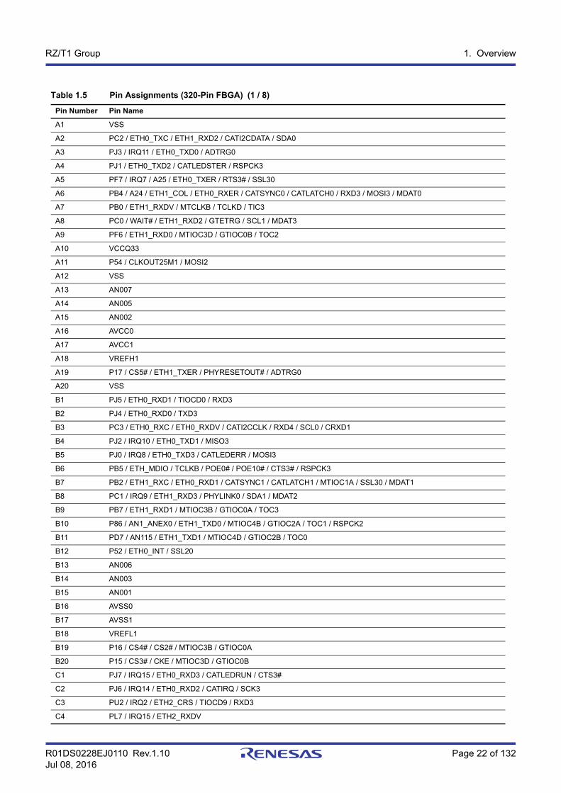
Table 1.5 Pin Assignments (320-Pin FBGA) (1 / 8)
Pin Number Pin Name
A1 VSS
A2 PC2 / ETH0_TXC / ETH1_RXD2 / CATI2CDATA / SDA0
A3 PJ3 / IRQ11 / ETH0_TXD0 / ADTRG0
A4 PJ1 / ETH0_TXD2 / CATLEDSTER / RSPCK3
A5 PF7 / IRQ7 / A25 / ETH0_TXER / RTS3# / SSL30
A6 PB4 / A24 / ETH1_COL / ETH0_RXER / CATSYNC0 / CATLATCH0 / RXD3 / MOSI3 / MDAT0
A7 PB0 / ETH1_RXDV / MTCLKB / TCLKD / TIC3
A8 PC0 / WAIT# / ETH1_RXD2 / GTETRG / SCL1 / MDAT3
A9 PF6 / ETH1_RXD0 / MTIOC3D / GTIOC0B / TOC2
A10 VCCQ33
A11 P54 / CLKOUT25M1 / MOSI2
A12 VSS
A13 AN007
A14 AN005
A15 AN002
A16 AVCC0
A17 AVCC1
A18 VREFH1
A19 P17 / CS5# / ETH1_TXER / PHYRESETOUT# / ADTRG0
A20 VSS
B1 PJ5 / ETH0_RXD1 / TIOCD0 / RXD3
B2 PJ4 / ETH0_RXD0 / TXD3
B3 PC3 / ETH0_RXC / ETH0_RXDV / CATI2CCLK / RXD4 / SCL0 / CRXD1
B4 PJ2 / IRQ10 / ETH0_TXD1 / MISO3
B5 PJ0 / IRQ8 / ETH0_TXD3 / CATLEDERR / MOSI3
B6 PB5 / ETH_MDIO / TCLKB / POE0# / POE10# / CTS3# / RSPCK3
B7 PB2 / ETH1_RXC / ETH0_RXD1 / CATSYNC1 / CATLATCH1 / MTIOC1A / SSL30 / MDAT1
B8 PC1 / IRQ9 / ETH1_RXD3 / PHYLINK0 / SDA1 / MDAT2
B9 PB7 / ETH1_RXD1 / MTIOC3B / GTIOC0A / TOC3
B10 P86 / AN1_ANEX0 / ETH1_TXD0 / MTIOC4B / GTIOC2A / TOC1 / RSPCK2
B11 PD7 / AN115 / ETH1_TXD1 / MTIOC4D / GTIOC2B / TOC0
B12 P52 / ETH0_INT / SSL20
B13 AN006
B14 AN003
B15 AN001
B16 AVSS0
B17 AVSS1
B18 VREFL1
B19 P16 / CS4# / CS2# / MTIOC3B / GTIOC0A
B20 P15 / CS3# / CKE / MTIOC3D / GTIOC0B
C1 PJ7 / IRQ15 / ETH0_RXD3 / CATLEDRUN / CTS3#
C2 PJ6 / IRQ14 / ETH0_RXD2 / CATIRQ / SCK3
C3 PU2 / IRQ2 / ETH2_CRS / TIOCD9 / RXD3
C4 PL7 / IRQ15 / ETH2_RXDV
R01DS0228EJ0110 Rev.1.10 Page 23 of 132Jul 08, 2016
RZ/T1 Group 1. Overview
C5 PL5 / ETH2_RXD2 / TIOCA8
C6 PB6 / ETH_MDC / TCLKA / SCK3 / RTS4# / MISO3
C7 PB3 / IRQ3 / CS1# / ETH1_CRS / PHYRESETOUT# / TXD3 / CTXD1 / MCLK0
C8 PB1 / ETH1_RXER / MTCLKA / TCLKC / CTS4#
C9 PF5 / ETH1_TXEN / MTIOC4A / GTIOC1A / TIC2
C10 P87 / AN1_ANEX1 / A23 / ETH1_TXC / ETH0_RXD0 / MTIOC4C / GTIOC1B / MCLK1
C11 PD6 / AN114 / A22 / ETH1_TXD2 / ETH0_TXD1 / TIC1 / MISO2 / MCLK2
C12 P53 / ETH1_INT / MISO2
C13 P51 / IRQ1 / PHYLINK1 / RSPCK2
C14 AN004
C15 AN000
C16 VREFL0
C17 VREFH0
C18 PD2 / AN110 / WAIT#
C19 P14 / CAS# / MTIOC4A / GTIOC1A
C20 P13 / RAS# / MTIOC4C / GTIOC1B
D1 P81 / ETH0_RXER / TIOCC0 / CTS4#
D2 P80 / IRQ8 / ETH0_RXDV / TIOCC3 / RTS4#
D3 PU3 / ETH2_COL / TIOCD6 / TXD3
D18 PD0 / AN108 / CS4#
D19 P96 / AN106 / POE0# / POE10#
D20 P95 / AN105 / IRQ13 / MTCLKA / CTS2#
E1 P84 / ETH0_COL / CATLINKACT1 / RXD4
E2 P82 / ETH0_TXEN / ETH1_CRS / TIOCD3 / SCK4 / RTS3# / USB_OVRCUR
E3 PU1 / ETH2_RXC / TIOCA11 / SCK3
E5 PU0 / ETH2_RXER / TIOCA10
E6 PL6 / ETH2_RXD3 / TIOCA9
E7 PL4 / IRQ4 / ETH2_RXD1
E8 PL2 / ETH2_TXEN / TIOCA6 / ADTRG1
E9 PL0 / ETH2_TXD0 / TIOCB9
E10 PK7 / ETH2_TXD2 / TIOCB7
E11 PK6 / ETH2_TXD3 / TIOCB6
E12 PD5 / AN113 / A21 / ETH1_TXD3 / ETH0_TXD0 / TIC0 / SSL20 / MCLK3
E13 P56 / BS# / ETH1_TXER
E14 PD4 / AN112 / ETH2_INT
E15 VCCQ33
E16 PD1 / AN109 / CS1#
E18 P97 / AN107 / IRQ7 / A25 / ADTRG1
E19 P94 / AN104 / IRQ4 / MTCLKB / RTS2#
E20 P93 / AN103 / MTIOC1A / TIC3 / SCK2 / ENCIF07
F1 PC4 / CATI2CCLK / TCLKH / SCL0
F2 P83 / IRQ11 / ETH0_CRS / CATLINKACT0 / TXD4
F3 P85 / IRQ5 / CLKOUT25M0 / TXD4 / SCK4 / USB_VBUSEN
F5 PU4 / MII2_MDC / TIOCC9 / CTS3#
F6 VSS
Table 1.5 Pin Assignments (320-Pin FBGA) (2 / 8)
Pin Number Pin Name

R01DS0228EJ0110 Rev.1.10 Page 24 of 132Jul 08, 2016
RZ/T1 Group 1. Overview
F7 VCCQ33
F8 PL3 / ETH2_RXD0 / TIOCA7
F9 PL1 / ETH2_TXC / TIOCB10
F10 PK5 / ETH2_TXD1 / TIOCB8
F11 PK4 / ETH2_TXER / TIOCB11 / MOSI2
F12 P55 / IRQ5 / A24 / ETHSWSECOUT
F13 P50 / IRQ8 / CS1# / PHYLINK0
F14 PD3 / AN111 / PHYRESETOUT2#
F15 PK2 / A23
F16 P90 / AN100 / RAS# / TIOCA5 / TXD4
F18 P92 / AN102 / CS5# / TOC3 / RXD2
F19 P91 / AN101 / CAS# / TXD2 / ENCIF06
F20 P12 / MTIOC4B / GTIOC2A
G1 PU6 / PHYRESETOUT# / TCLKF / CTS4#
G2 PC5 / CATI2CDATA / TCLKG / SDA0
G3 VCCQ33
G5 PU5 / IRQ13 / MII2_MDIO / TIOCC6 / RTS3#
G6 PM0 / CLKOUT25M2 / TXD4
G15 PK3 / A24
G16 PA7 / IRQ7 / D31 / A22 / MTIOC6B / GTIOC3B / RTS2# / MCLK0
G18 PA4 / D28 / ETH1_INT / TIOCA3 / ADTRG0 / RXD2 / TEND2 / MDAT1
G19 PA3 / D27 / ETHSWSECOUT / GTETRG / TIOCA2 / SCK2 / DACK2 / MCLK2
G20 P11 / IRQ9 / MTIOC4D / GTIOC2B
H1 PU7 / CATIRQ / RXD4
H2 PM1 / CATLEDERR / SCK4
H3 P35 / NMI
H5 ERROROUT#
H6 VCCQ33
H8 VDD
H9 VDD
H10 VDD
H11 VDD
H12 VDD
H13 VSS
H15 PA6 / IRQ6 / D30 / A21 / GTIOC3A / CTS2# / MDAT0
H16 PA5 / D29 / ETH0_INT / ETH1_TXER / TIOCA4 / TXD2 / MCLK1
H18 PA2 / D26 / MTIOC3B / GTIOC0A / SSL02 / DREQ2 / MDAT2/ ENCIF05
H19 PK0 / CAS# / PO31
H20 PK1 / CS5#
J1 PM6 / IRQ6 / CATLINKACT0 / PO19
J2 PM3 / CATSYNC0 / CATLATCH0 / PO16
J3 PM2 / CATSYNC1 / CATLATCH1 / TCLKE / RTS4#
J5 P33 / TDO
J6 TRST#
J8 VDD
Table 1.5 Pin Assignments (320-Pin FBGA) (3 / 8)
Pin Number Pin Name
R01DS0228EJ0110 Rev.1.10 Page 25 of 132Jul 08, 2016
RZ/T1 Group 1. Overview
J9 VSS
J10 VSS
J11 VSS
J12 VSS
J13 VDD
J15 VCCQ33
J16 PA1 / D25 / MTIOC3D / GTIOC0B / MISO0 / AUDIO_CLK / TRACEDATA7 / MCLK3
J18 PA0 / D24 / MTIOC4A / GTIOC1A / MOSI0 / TRACEDATA6 / MDAT3
J19 PT7 / A22 / DACK2
J20 PT6 / A21 / DREQ2
K1 PM7 / CATLINKACT1 / PO20
K2 PM5 / CATLEDSTER / PO18
K3 PM4 / CATLEDRUN / PO17
K5 P34 / TDI
K6 PLLVDD1
K8 VDD
K9 VSS
K10 VSS
K11 VSS
K12 VSS
K13 VDD
K15 VSS
K16 P77 / D23 / MTIOC4C / GTIOC1B / RSPCK0 / TRACEDATA5
K18 P76 / D22 / MTIOC4B / GTIOC2A / SSL01 / SSIWS0 / TRACEDATA4
K19 P75 / IRQ13 / D21 / MTIOC4D / GTIOC2B / SSL00 / TRACEDATA3/ ENCIF04
K20 PT5 / BS# / PO30 / TEND2
L1 MD1
L2 MD2
L3 TMS
L5 TCK
L6 PLLVSS1
L8 VDD
L9 VSS
L10 VSS
L11 VSS
L12 VSS
L13 VDD
L15 VSS
L16 PE7 / D15 / MTIOC7A / TIOCD3 / POE8# / SCK1 / RSPCK0 / TRACEDATA7
L18 P72 / D18 / MTIOC1A / TIC2 / TXD1 / SSITXD0 / TRACEDATA0 / ENCIF02
L19 P73 / IRQ3 / D19 / MTCLKB / RXD1 / SSIRXD0 / TRACEDATA1 / ENCIF03
L20 P74 / D20 / MTCLKA / CTS1# / SSL03 / SSISCK0 / TRACEDATA2
M1 XTAL
M2 EXTAL
M3 OSCTH
Table 1.5 Pin Assignments (320-Pin FBGA) (4 / 8)
Pin Number Pin Name

R01DS0228EJ0110 Rev.1.10 Page 26 of 132Jul 08, 2016
RZ/T1 Group 1. Overview
M5 BSCANP
M6 PLLVDD0
M8 VDD
M9 VSS
M10 VSS
M11 VSS
M12 VSS
M13 VDD
M15 VCCQ33
M16 PE6 / IRQ6 / D14 / MTIOC0A / TIOCD0 / RXD1 / MISO0 / TRACEDATA6
M18 P70 / IRQ0 / D16 / MTIOC6D / RTS1# / USB_OVRCUR / TRACECLK / ENCIF00
M19 PT4 / CS3# / PO29
M20 P71 / D17 / POE0# / POE10# / TOC2 / SCK1 / TRACECTL / ENCIF01
N1 VSS
N2 MD0
N3 RSTOUT#
N5 RES#
N6 PLLVSS0
N8 VDD
N9 VSS
N10 VDD
N11 VDD
N12 VDD
N13 VDD
N15 PE2 / IRQ2 / D10 / MTCLKC / TIOCB4 / SSL02 / TRACEDATA2
N16 PE4 / D12 / MTIOC0B / TIOCC0 / RTS1# / SSL00 / TRACEDATA4
N18 PE5 / D13 / MTIOC0C / TIOCC3 / TXD1 / MOSI0 / TRACEDATA5
N19 PT2 / TIOCA1 / TIOCB1 / PO27
N20 PT3 / IRQ11 / TIOCA0 / TIOCB0 / PO28 / CTS2#
P1 VSS_USB
P2 VDD33_USB
P3 USB_RREF
P5 P31 / USB_VBUSEN
P6 VCCQ33
P15 P06 / D6 / MTIOC2B / TIOCB0
P16 P07 / D7 / MTIOC2A / TIOCB1
P18 PE3 / IRQ3 / D11 / MTIOC0D / TIOCB5 / CTS1# / SSL01 / TRACEDATA3
P19 PT0 / IRQ0 / TIOCA3 / TIOCB3 / PO25 / SCK2 / ENCIF07
P20 PT1 / TIOCA2 / TIOCB2 / PO26 / RTS2#
R1 USB_DP
R2 USB_DM
R3 P30 / CRXD0 / USB_VBUSIN
R5 PN0 / MTIOC8D / SSL10
R6 PN2 / IRQ10 / MTIOC8B / MOSI1
R7 PG0 / A1 / PO2
Table 1.5 Pin Assignments (320-Pin FBGA) (5 / 8)
Pin Number Pin Name
R01DS0228EJ0110 Rev.1.10 Page 27 of 132Jul 08, 2016
RZ/T1 Group 1. Overview
R8 PG2 / A3 / PO4 / TOC0 / RSPCK1
R9 PG7 / A8 / PO9
R10 PH2 / A11 / MTIOC2A / PO12
R11 PH4 / IRQ4 / A13 / PO14
R12 PH6 / A15 / MTIOC7D / RTS0#
R13 P23 / A0 / MTIC5U / TXD0 / DACK1
R14 P27 / A20 / MTIOC8C / TIOCB0 / RTS0#
R15 P47 / WE3#/DQMUU/AH# / MTIOC6C
R16 VCCQ33
R18 VCCQ33
R19 PS6 / IRQ14 / TIOCA5 / TIOCB5 / PO23 / RXD2 / ENCIF06
R20 PS7 / TIOCA4 / TIOCB4 / PO24 / TXD2
T1 DVDD_USB
T2 VDD33_USB
T3 P32 / IRQ10 / USB_OVRCUR
T5 PC6 / TCLKC / SCL1 / CRXD0 / DREQ0 / USB_VBUSIN
T6 P37 / WE1#/DQMLU / PO1
T7 P36 / WE0#/DQMLL / PO0
T8 PG3 / A4 / PO5 / TIC1 / MISO1
T9 PG6 / A7 / TCLKB / PO8 / SSL11
T10 PH3 / A12 / MTIOC1B / PO13
T11 VCCQ33
T12 PH5 / A14 / PO15
T13 VCCQ33
T14 P26 / A19 / MTIOC8D / DREQ1
T15 VCCQ33
T16 VSS
T18 VSS
T19 PE0 / D8 / MTIOC1B / TIOCB2 / TRACEDATA0
T20 PE1 / D9 / MTCLKD / TIOCB3 / SSL03 / TRACEDATA1
U1 P60 / SPBSSL / CTXD0 / TEND0
U2 P63 / SPBMO/SPBIO0
U3 PN1 / MTIOC8C / PO21 / MISO1
U18 P00 / D0 / MTIOC6A / TIOCA1 / ADTRG1 / TRACECTL
U19 P04 / D4 / MTIOC3C / TIOCA5
U20 P03 / D3 / MTIC5U / TIOCA4
V1 P61 / SPBIO3 / CTXD1 / DACK0
V2 P64 / SPBMI/SPBIO1
V3 PN3 / MTIOC8A / RSPCK1
V4 PN4 / IRQ12 / MTIOC6C / TIOCC6 / SSL11
V5 PC7 / TIC0 / SDA1 / CRXD1
V6 PG1 / A2 / PO3
V7 PG4 / A5 / PO6 / TOC1 / MOSI1
V8 PG5 / A6 / TCLKA / PO7 / SSL10
V9 PH0 / A9 / PO10
Table 1.5 Pin Assignments (320-Pin FBGA) (6 / 8)
Pin Number Pin Name

R01DS0228EJ0110 Rev.1.10 Page 28 of 132Jul 08, 2016
RZ/T1 Group 1. Overview
V10 PH1 / A10 / MTIOC2B / PO11
V11 PH7 / A16 / MTIC5W
V12 P20 / A17 / MTCLKD
V13 P21 / IRQ1 / CS0# / MTIC5V / TIOCB1 / CTS0#
V14 VSS
V15 P45 / CS2#
V16 P46 / CKE
V17 PS2 / MTIOC7C / SSIWS0
V18 P05 / D5 / MTIOC3A
V19 P01 / D1 / MTIC5W / TIOCA2
V20 P02 / D2 / MTIC5V / TIOCA3
W1 P62 / SPBCLK
W2 P65 / SPBIO2 / DREQ0
W3 PN5 / IRQ5 / MTIOC6A / TIOCD9
W4 PN6 / MTIOC3C / TIOCC9 / MCLK3
W5 PP0 / POE8# / TEND0 / MCLK2
W6 PP2 / MTIOC0C / TCLKH / MCLK1
W7 PP4 / MTIOC0A / MCLK0
W8 PP6 / TIOCA11 / RXD1 / TRACECTL / ENCIF06
W9 PP7 / TCLKF / TCLKH / SCK1 / DACK1 / TRACECLK
W10 PR1 / IRQ9 / POE4# / CTS1# / TEND1 / TRACEDATA1
W11 PR3 / TIOCA10 / TIOCB10 / TRACEDATA3 / ENCIF01
W12 PR5 / TIOCA8 / TIOCB8 / TRACEDATA5 / ENCIF03
W13 P24 / IRQ12 / RD/WR# / RXD0
W14 P22 / IRQ2 / RD# / MTIOC7B / TIOCD0 / SCK0
W15 P44 / IRQ12 / WAIT# / TCLKD / ADTRG0 / CTS0#
W16 P43 / WE2#/DQMUL / MTIOC8B / USB_VBUSEN
W17 PS1 / IRQ1 / MTIOC7B / SSISCK0
W18 PS3 / MTIOC7A / SSIRXD0
W19 PS4 / MTIOC6D / SSITXD0
W20 PS5 / MTIOC6B
Y1 VSS
Y2 P67 / IRQ15 / GTIOC3B / CTXD0 / TEND0 / USB_OVRCUR
Y3 P66 / IRQ14 / GTIOC3A / CTXD1 / DACK0 / USB_VBUSEN
Y4 PN7 / MTIOC3A / TIOCD6 / DREQ0 / MDAT3
Y5 PP1 / MTIOC0D / DACK0 / MDAT2
Y6 PP3 / MTIOC0B / TCLKC / MDAT1
Y7 PP5 / PO22 / MDAT0
Y8 VSS
Y9 PR0 / TCLKE / TCLKG / TXD1 / DREQ1 / TRACEDATA0 / ENCIF07
Y10 PR2 / TIOCA11 / TIOCB11 / RTS1# / TRACEDATA2 / ENCIF00
Y11 PR4 / TIOCA9 / TIOCB9 / TRACEDATA4 / ENCIF02
Y12 PR6 / TIOCA7 / TIOCB7 / TRACEDATA6 / ENCIF04
Y13 PR7 / TIOCA6 / TIOCB6 / TRACEDATA7 / ENCIF05
Y14 P25 / A18 / MTCLKC / TEND1
Table 1.5 Pin Assignments (320-Pin FBGA) (7 / 8)
Pin Number Pin Name
R01DS0228EJ0110 Rev.1.10 Page 29 of 132Jul 08, 2016
RZ/T1 Group 1. Overview
Y15 P41 / BS# / SCK0
Y16 P42 / MTIOC7C / RXD0
Y17 P40 / MTIOC8A / TXD0
Y18 PS0 / MTIOC7D / AUDIO_CLK
Y19 P10 / IRQ0 / CKIO / TIOCA0 / TRACECLK
Y20 VSS
Table 1.5 Pin Assignments (320-Pin FBGA) (8 / 8)
Pin Number Pin Name
R01DS0228EJ0110 Rev.1.10 Page 30 of 132Jul 08, 2016
RZ/T1 Group 1. Overview
Table 1.6 Pin Assignments (176-Pin HLQFP) (1 / 4)
Pin Number Pin Name
1 PC3 / ETH0_RXC / ETH0_RXDV / RXD4 / SCL0 / CRXD1
2 VCCQ33
3 VSS
4 VDD
5 P82 / ETH0_TXEN / ETH1_CRS / TIOCD3 / SCK4 / RTS3# / USB_OVRCUR
6 P85 / IRQ5 / CLKOUT25M0 / TXD4 / SCK4 / USB_VBUSEN
7 ERROROUT#
8 P35 / NMI
9 TRST#
10 P33 / TDO
11 P34 / TDI
12 TMS
13 TCK
14 BSCANP
15 VDD
16 VSS
17 MD2
18 MD1
19 PLLVDD1
20 PLLVSS1
21 OSCTH
22 VCCQ33
23 EXTAL
24 XTAL
25 VSS
26 MD0
27 PLLVDD0
28 PLLVSS0
29 RES#
30 RSTOUT#
31 VDD
32 VSS
33 VDD33_USB
34 VSS_USB
35 USB_RREF
36 USB_DM
37 USB_DP
38 VDD33_USB
39 DVDD_USB
40 P30 / CRXD0 / USB_VBUSIN
41 P60 / SPBSSL / CTXD0 / TEND0
42 P61 / SPBIO3 / CTXD1 / DACK0
43 VCCQ33
44 P62 / SPBCLK
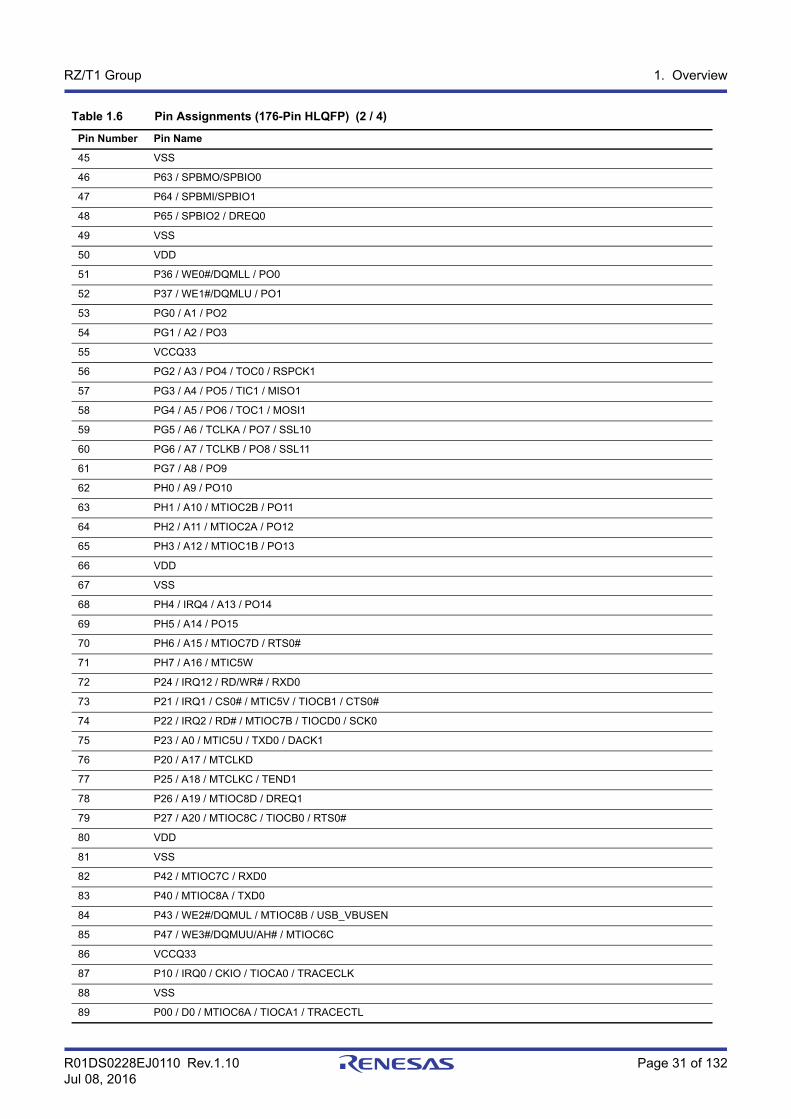
R01DS0228EJ0110 Rev.1.10 Page 31 of 132Jul 08, 2016
RZ/T1 Group 1. Overview
45 VSS
46 P63 / SPBMO/SPBIO0
47 P64 / SPBMI/SPBIO1
48 P65 / SPBIO2 / DREQ0
49 VSS
50 VDD
51 P36 / WE0#/DQMLL / PO0
52 P37 / WE1#/DQMLU / PO1
53 PG0 / A1 / PO2
54 PG1 / A2 / PO3
55 VCCQ33
56 PG2 / A3 / PO4 / TOC0 / RSPCK1
57 PG3 / A4 / PO5 / TIC1 / MISO1
58 PG4 / A5 / PO6 / TOC1 / MOSI1
59 PG5 / A6 / TCLKA / PO7 / SSL10
60 PG6 / A7 / TCLKB / PO8 / SSL11
61 PG7 / A8 / PO9
62 PH0 / A9 / PO10
63 PH1 / A10 / MTIOC2B / PO11
64 PH2 / A11 / MTIOC2A / PO12
65 PH3 / A12 / MTIOC1B / PO13
66 VDD
67 VSS
68 PH4 / IRQ4 / A13 / PO14
69 PH5 / A14 / PO15
70 PH6 / A15 / MTIOC7D / RTS0#
71 PH7 / A16 / MTIC5W
72 P24 / IRQ12 / RD/WR# / RXD0
73 P21 / IRQ1 / CS0# / MTIC5V / TIOCB1 / CTS0#
74 P22 / IRQ2 / RD# / MTIOC7B / TIOCD0 / SCK0
75 P23 / A0 / MTIC5U / TXD0 / DACK1
76 P20 / A17 / MTCLKD
77 P25 / A18 / MTCLKC / TEND1
78 P26 / A19 / MTIOC8D / DREQ1
79 P27 / A20 / MTIOC8C / TIOCB0 / RTS0#
80 VDD
81 VSS
82 P42 / MTIOC7C / RXD0
83 P40 / MTIOC8A / TXD0
84 P43 / WE2#/DQMUL / MTIOC8B / USB_VBUSEN
85 P47 / WE3#/DQMUU/AH# / MTIOC6C
86 VCCQ33
87 P10 / IRQ0 / CKIO / TIOCA0 / TRACECLK
88 VSS
89 P00 / D0 / MTIOC6A / TIOCA1 / TRACECTL
Table 1.6 Pin Assignments (176-Pin HLQFP) (2 / 4)
Pin Number Pin Name
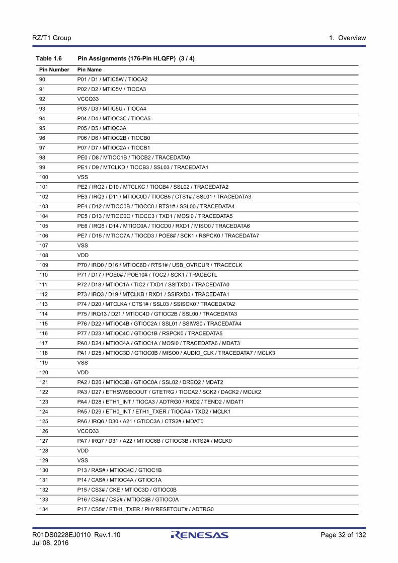
R01DS0228EJ0110 Rev.1.10 Page 32 of 132Jul 08, 2016
RZ/T1 Group 1. Overview
90 P01 / D1 / MTIC5W / TIOCA2
91 P02 / D2 / MTIC5V / TIOCA3
92 VCCQ33
93 P03 / D3 / MTIC5U / TIOCA4
94 P04 / D4 / MTIOC3C / TIOCA5
95 P05 / D5 / MTIOC3A
96 P06 / D6 / MTIOC2B / TIOCB0
97 P07 / D7 / MTIOC2A / TIOCB1
98 PE0 / D8 / MTIOC1B / TIOCB2 / TRACEDATA0
99 PE1 / D9 / MTCLKD / TIOCB3 / SSL03 / TRACEDATA1
100 VSS
101 PE2 / IRQ2 / D10 / MTCLKC / TIOCB4 / SSL02 / TRACEDATA2
102 PE3 / IRQ3 / D11 / MTIOC0D / TIOCB5 / CTS1# / SSL01 / TRACEDATA3
103 PE4 / D12 / MTIOC0B / TIOCC0 / RTS1# / SSL00 / TRACEDATA4
104 PE5 / D13 / MTIOC0C / TIOCC3 / TXD1 / MOSI0 / TRACEDATA5
105 PE6 / IRQ6 / D14 / MTIOC0A / TIOCD0 / RXD1 / MISO0 / TRACEDATA6
106 PE7 / D15 / MTIOC7A / TIOCD3 / POE8# / SCK1 / RSPCK0 / TRACEDATA7
107 VSS
108 VDD
109 P70 / IRQ0 / D16 / MTIOC6D / RTS1# / USB_OVRCUR / TRACECLK
110 P71 / D17 / POE0# / POE10# / TOC2 / SCK1 / TRACECTL
111 P72 / D18 / MTIOC1A / TIC2 / TXD1 / SSITXD0 / TRACEDATA0
112 P73 / IRQ3 / D19 / MTCLKB / RXD1 / SSIRXD0 / TRACEDATA1
113 P74 / D20 / MTCLKA / CTS1# / SSL03 / SSISCK0 / TRACEDATA2
114 P75 / IRQ13 / D21 / MTIOC4D / GTIOC2B / SSL00 / TRACEDATA3
115 P76 / D22 / MTIOC4B / GTIOC2A / SSL01 / SSIWS0 / TRACEDATA4
116 P77 / D23 / MTIOC4C / GTIOC1B / RSPCK0 / TRACEDATA5
117 PA0 / D24 / MTIOC4A / GTIOC1A / MOSI0 / TRACEDATA6 / MDAT3
118 PA1 / D25 / MTIOC3D / GTIOC0B / MISO0 / AUDIO_CLK / TRACEDATA7 / MCLK3
119 VSS
120 VDD
121 PA2 / D26 / MTIOC3B / GTIOC0A / SSL02 / DREQ2 / MDAT2
122 PA3 / D27 / ETHSWSECOUT / GTETRG / TIOCA2 / SCK2 / DACK2 / MCLK2
123 PA4 / D28 / ETH1_INT / TIOCA3 / ADTRG0 / RXD2 / TEND2 / MDAT1
124 PA5 / D29 / ETH0_INT / ETH1_TXER / TIOCA4 / TXD2 / MCLK1
125 PA6 / IRQ6 / D30 / A21 / GTIOC3A / CTS2# / MDAT0
126 VCCQ33
127 PA7 / IRQ7 / D31 / A22 / MTIOC6B / GTIOC3B / RTS2# / MCLK0
128 VDD
129 VSS
130 P13 / RAS# / MTIOC4C / GTIOC1B
131 P14 / CAS# / MTIOC4A / GTIOC1A
132 P15 / CS3# / CKE / MTIOC3D / GTIOC0B
133 P16 / CS4# / CS2# / MTIOC3B / GTIOC0A
134 P17 / CS5# / ETH1_TXER / PHYRESETOUT# / ADTRG0
Table 1.6 Pin Assignments (176-Pin HLQFP) (3 / 4)
Pin Number Pin Name

R01DS0228EJ0110 Rev.1.10 Page 33 of 132Jul 08, 2016
RZ/T1 Group 1. Overview
135 VCCQ33
136 VREFH0
137 VREFL0
138 AVSS0
139 AVCC0
140 AN000
141 AN001
142 AN002
143 AN003
144 AN004
145 AN005
146 AN006
147 AN007
148 VDD
149 VSS
150 P51 / IRQ1 / PHYLINK1 / RSPCK2
151 P54 / CLKOUT25M1 / MOSI2
152 P56 / BS# / ETH1_TXER
153 PD5 / A21 / ETH1_TXD3 / ETH0_TXD0 / TIC0 / SSL20 / MCLK3
154 PD6 / A22 / ETH1_TXD2 / ETH0_TXD1 / TIC1 / MISO2 / MCLK2
155 PD7 / ETH1_TXD1 / MTIOC4D / GTIOC2B / TOC0
156 P86 / ETH1_TXD0 / MTIOC4B / GTIOC2A / TOC1 / RSPCK2
157 P87 / A23 / ETH1_TXC / ETH0_RXD0 / MTIOC4C / GTIOC1B / MCLK1
158 PF5 / ETH1_TXEN / MTIOC4A / GTIOC1A / TIC2
159 VCCQ33
160 VDD
161 VSS
162 PF6 / ETH1_RXD0 / MTIOC3D / GTIOC0B / TOC2
163 PB7 / ETH1_RXD1 / MTIOC3B / GTIOC0A / TOC3
164 PC0 / WAIT# / ETH1_RXD2 / GTETRG / SCL1 / MDAT3
165 PC1 / IRQ9 / ETH1_RXD3 / PHYLINK0 / SDA1 / MDAT2
166 PB0 / ETH1_RXDV / MTCLKB / TCLKD / TIC3
167 PB1 / ETH1_RXER / MTCLKA / TCLKC / CTS4#
168 PB2 / ETH1_RXC / ETH0_RXD1 / MTIOC1A / SSL30 / MDAT1
169 VCCQ33
170 PB3 / IRQ3 / CS1# / ETH1_CRS / PHYRESETOUT# / TXD3 / CTXD1 / MCLK0
171 PB4 / A24 / ETH1_COL / ETH0_RXER / RXD3 / MOSI3 / MDAT0
172 PB5 / ETH_MDIO / TCLKB / POE0# / POE10# / CTS3# / RSPCK3
173 VSS
174 VDD
175 PB6 / ETH_MDC / TCLKA / SCK3 / RTS4# / MISO3
176 PC2 / ETH0_TXC / ETH1_RXD2 / SDA0
Table 1.6 Pin Assignments (176-Pin HLQFP) (4 / 4)
Pin Number Pin Name
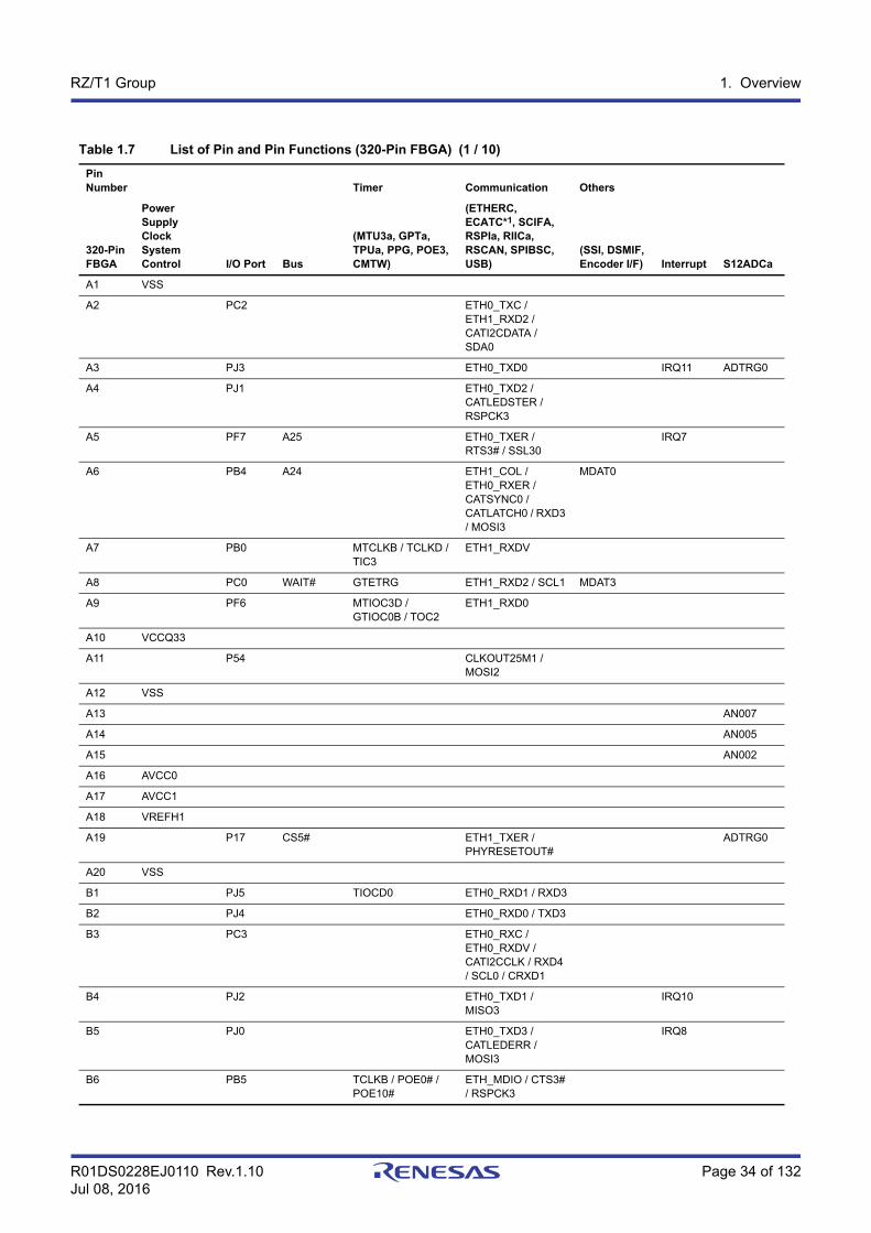
R01DS0228EJ0110 Rev.1.10 Page 34 of 132Jul 08, 2016
RZ/T1 Group 1. Overview
Table 1.7 List of Pin and Pin Functions (320-Pin FBGA) (1 / 10)
PinNumber
PowerSupplyClockSystemControl I/O Port Bus
Timer Communication Others
Interrupt S12ADCa320-PinFBGA
(MTU3a, GPTa, TPUa, PPG, POE3, CMTW)
(ETHERC, ECATC*1, SCIFA, RSPIa, RIICa, RSCAN, SPIBSC, USB)
(SSI, DSMIF,Encoder I/F)
A1 VSS
A2 PC2 ETH0_TXC / ETH1_RXD2 / CATI2CDATA / SDA0
A3 PJ3 ETH0_TXD0 IRQ11 ADTRG0
A4 PJ1 ETH0_TXD2 / CATLEDSTER / RSPCK3
A5 PF7 A25 ETH0_TXER / RTS3# / SSL30
IRQ7
A6 PB4 A24 ETH1_COL / ETH0_RXER / CATSYNC0 / CATLATCH0 / RXD3 / MOSI3
MDAT0
A7 PB0 MTCLKB / TCLKD / TIC3
ETH1_RXDV
A8 PC0 WAIT# GTETRG ETH1_RXD2 / SCL1 MDAT3
A9 PF6 MTIOC3D / GTIOC0B / TOC2
ETH1_RXD0
A10 VCCQ33
A11 P54 CLKOUT25M1 / MOSI2
A12 VSS
A13 AN007
A14 AN005
A15 AN002
A16 AVCC0
A17 AVCC1
A18 VREFH1
A19 P17 CS5# ETH1_TXER / PHYRESETOUT#
ADTRG0
A20 VSS
B1 PJ5 TIOCD0 ETH0_RXD1 / RXD3
B2 PJ4 ETH0_RXD0 / TXD3
B3 PC3 ETH0_RXC / ETH0_RXDV / CATI2CCLK / RXD4 / SCL0 / CRXD1
B4 PJ2 ETH0_TXD1 / MISO3
IRQ10
B5 PJ0 ETH0_TXD3 / CATLEDERR / MOSI3
IRQ8
B6 PB5 TCLKB / POE0# / POE10#
ETH_MDIO / CTS3# / RSPCK3

R01DS0228EJ0110 Rev.1.10 Page 35 of 132Jul 08, 2016
RZ/T1 Group 1. Overview
B7 PB2 MTIOC1A ETH1_RXC / ETH0_RXD1 / CATSYNC1 / CATLATCH1 / SSL30
MDAT1
B8 PC1 ETH1_RXD3 / PHYLINK0 / SDA1
MDAT2 IRQ9
B9 PB7 MTIOC3B / GTIOC0A / TOC3
ETH1_RXD1
B10 P86 MTIOC4B / GTIOC2A / TOC1
ETH1_TXD0 / RSPCK2
AN1_ANEX0
B11 PD7 MTIOC4D / GTIOC2B / TOC0
ETH1_TXD1 AN115
B12 P52 ETH0_INT / SSL20
B13 AN006
B14 AN003
B15 AN001
B16 AVSS0
B17 AVSS1
B18 VREFL1
B19 P16 CS4# / CS2#
MTIOC3B / GTIOC0A
B20 P15 CS3# / CKE MTIOC3D / GTIOC0B
C1 PJ7 ETH0_RXD3 / CATLEDRUN / CTS3#
IRQ15
C2 PJ6 ETH0_RXD2 / CATIRQ / SCK3
IRQ14
C3 PU2 TIOCD9 ETH2_CRS / RXD3 IRQ2
C4 PL7 ETH2_RXDV IRQ15
C5 PL5 TIOCA8 ETH2_RXD2
C6 PB6 TCLKA ETH_MDC / SCK3 / RTS4# / MISO3
C7 PB3 CS1# ETH1_CRS / PHYRESETOUT# / TXD3 / CTXD1
MCLK0 IRQ3
C8 PB1 MTCLKA / TCLKC ETH1_RXER / CTS4#
C9 PF5 MTIOC4A / GTIOC1A / TIC2
ETH1_TXEN
C10 P87 A23 MTIOC4C / GTIOC1B
ETH1_TXC / ETH0_RXD0
MCLK1 AN1_ANEX1
C11 PD6 A22 TIC1 ETH1_TXD2 / ETH0_TXD1 / MISO2
MCLK2 AN114
C12 P53 ETH1_INT / MISO2
C13 P51 PHYLINK1 / RSPCK2
IRQ1
C14 AN004
Table 1.7 List of Pin and Pin Functions (320-Pin FBGA) (2 / 10)
PinNumber
PowerSupplyClockSystemControl I/O Port Bus
Timer Communication Others
Interrupt S12ADCa320-PinFBGA
(MTU3a, GPTa, TPUa, PPG, POE3, CMTW)
(ETHERC, ECATC*1, SCIFA, RSPIa, RIICa, RSCAN, SPIBSC, USB)
(SSI, DSMIF,Encoder I/F)
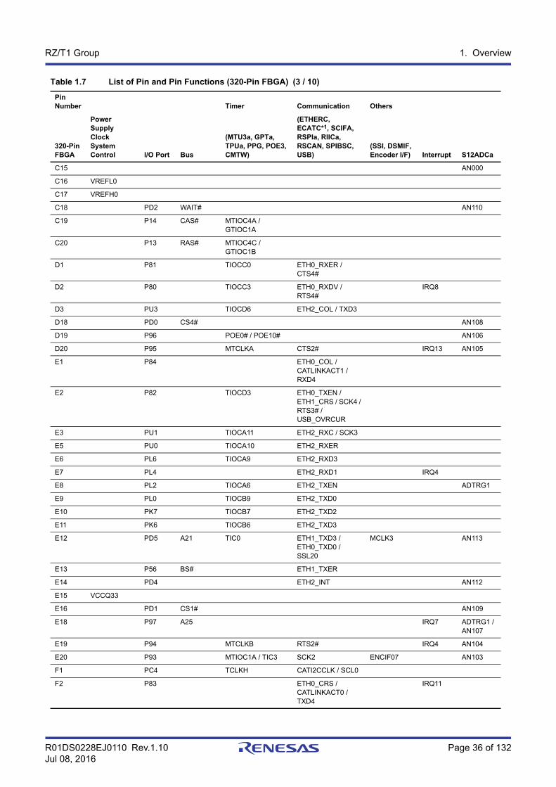
R01DS0228EJ0110 Rev.1.10 Page 36 of 132Jul 08, 2016
RZ/T1 Group 1. Overview
C15 AN000
C16 VREFL0
C17 VREFH0
C18 PD2 WAIT# AN110
C19 P14 CAS# MTIOC4A / GTIOC1A
C20 P13 RAS# MTIOC4C / GTIOC1B
D1 P81 TIOCC0 ETH0_RXER / CTS4#
D2 P80 TIOCC3 ETH0_RXDV / RTS4#
IRQ8
D3 PU3 TIOCD6 ETH2_COL / TXD3
D18 PD0 CS4# AN108
D19 P96 POE0# / POE10# AN106
D20 P95 MTCLKA CTS2# IRQ13 AN105
E1 P84 ETH0_COL / CATLINKACT1 / RXD4
E2 P82 TIOCD3 ETH0_TXEN / ETH1_CRS / SCK4 / RTS3# / USB_OVRCUR
E3 PU1 TIOCA11 ETH2_RXC / SCK3
E5 PU0 TIOCA10 ETH2_RXER
E6 PL6 TIOCA9 ETH2_RXD3
E7 PL4 ETH2_RXD1 IRQ4
E8 PL2 TIOCA6 ETH2_TXEN ADTRG1
E9 PL0 TIOCB9 ETH2_TXD0
E10 PK7 TIOCB7 ETH2_TXD2
E11 PK6 TIOCB6 ETH2_TXD3
E12 PD5 A21 TIC0 ETH1_TXD3 / ETH0_TXD0 / SSL20
MCLK3 AN113
E13 P56 BS# ETH1_TXER
E14 PD4 ETH2_INT AN112
E15 VCCQ33
E16 PD1 CS1# AN109
E18 P97 A25 IRQ7 ADTRG1 / AN107
E19 P94 MTCLKB RTS2# IRQ4 AN104
E20 P93 MTIOC1A / TIC3 SCK2 ENCIF07 AN103
F1 PC4 TCLKH CATI2CCLK / SCL0
F2 P83 ETH0_CRS / CATLINKACT0 / TXD4
IRQ11
Table 1.7 List of Pin and Pin Functions (320-Pin FBGA) (3 / 10)
PinNumber
PowerSupplyClockSystemControl I/O Port Bus
Timer Communication Others
Interrupt S12ADCa320-PinFBGA
(MTU3a, GPTa, TPUa, PPG, POE3, CMTW)
(ETHERC, ECATC*1, SCIFA, RSPIa, RIICa, RSCAN, SPIBSC, USB)
(SSI, DSMIF,Encoder I/F)
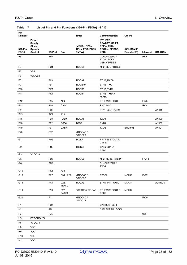
R01DS0228EJ0110 Rev.1.10 Page 37 of 132Jul 08, 2016
RZ/T1 Group 1. Overview
F3 P85 CLKOUT25M0 / TXD4 / SCK4 / USB_VBUSEN
IRQ5
F5 PU4 TIOCC9 MII2_MDC / CTS3#
F6 VSS
F7 VCCQ33
F8 PL3 TIOCA7 ETH2_RXD0
F9 PL1 TIOCB10 ETH2_TXC
F10 PK5 TIOCB8 ETH2_TXD1
F11 PK4 TIOCB11 ETH2_TXER / MOSI2
F12 P55 A24 ETHSWSECOUT IRQ5
F13 P50 CS1# PHYLINK0 IRQ8
F14 PD3 PHYRESETOUT2# AN111
F15 PK2 A23
F16 P90 RAS# TIOCA5 TXD4 AN100
F18 P92 CS5# TOC3 RXD2 AN102
F19 P91 CAS# TXD2 ENCIF06 AN101
F20 P12 MTIOC4B / GTIOC2A
G1 PU6 TCLKF PHYRESETOUT# / CTS4#
G2 PC5 TCLKG CATI2CDATA / SDA0
G3 VCCQ33
G5 PU5 TIOCC6 MII2_MDIO / RTS3# IRQ13
G6 PM0 CLKOUT25M2 / TXD4
G15 PK3 A24
G16 PA7 D31 / A22 MTIOC6B / GTIOC3B
RTS2# MCLK0 IRQ7
G18 PA4 D28 / TEND2
TIOCA3 ETH1_INT / RXD2 MDAT1 ADTRG0
G19 PA3 D27 / DACK2
GTETRG / TIOCA2 ETHSWSECOUT / SCK2
MCLK2
G20 P11 MTIOC4D / GTIOC2B
IRQ9
H1 PU7 CATIRQ / RXD4
H2 PM1 CATLEDERR / SCK4
H3 P35 NMI
H5 ERROROUT#
H6 VCCQ33
H8 VDD
H9 VDD
H10 VDD
H11 VDD
Table 1.7 List of Pin and Pin Functions (320-Pin FBGA) (4 / 10)
PinNumber
PowerSupplyClockSystemControl I/O Port Bus
Timer Communication Others
Interrupt S12ADCa320-PinFBGA
(MTU3a, GPTa, TPUa, PPG, POE3, CMTW)
(ETHERC, ECATC*1, SCIFA, RSPIa, RIICa, RSCAN, SPIBSC, USB)
(SSI, DSMIF,Encoder I/F)

R01DS0228EJ0110 Rev.1.10 Page 38 of 132Jul 08, 2016
RZ/T1 Group 1. Overview
H12 VDD
H13 VSS
H15 PA6 D30 / A21 GTIOC3A CTS2# MDAT0 IRQ6
H16 PA5 D29 TIOCA4 ETH0_INT / ETH1_TXER / TXD2
MCLK1
H18 PA2 D26 / DREQ2
MTIOC3B / GTIOC0A
SSL02 MDAT2 /ENCIF05
H19 PK0 CAS# PO31
H20 PK1 CS5#
J1 PM6 PO19 CATLINKACT0 IRQ6
J2 PM3 PO16 CATSYNC0 / CATLATCH0
J3 PM2 TCLKE CATSYNC1 / CATLATCH1 / RTS4#
J5 TDO P33
J6 TRST#
J8 VDD
J9 VSS
J10 VSS
J11 VSS
J12 VSS
J13 VDD
J15 VCCQ33
J16 TRACEDATA7 PA1 D25 MTIOC3D / GTIOC0B
MISO0 AUDIO_CLK / MCLK3
J18 TRACEDATA6 PA0 D24 MTIOC4A / GTIOC1A
MOSI0 MDAT3
J19 PT7 A22 / DACK2
J20 PT6 A21 / DREQ2
K1 PM7 PO20 CATLINKACT1
K2 PM5 PO18 CATLEDSTER
K3 PM4 PO17 CATLEDRUN
K5 TDI P34
K6 PLLVDD1
K8 VDD
K9 VSS
K10 VSS
K11 VSS
K12 VSS
K13 VDD
K15 VSS
K16 TRACEDATA5 P77 D23 MTIOC4C / GTIOC1B
RSPCK0
Table 1.7 List of Pin and Pin Functions (320-Pin FBGA) (5 / 10)
PinNumber
PowerSupplyClockSystemControl I/O Port Bus
Timer Communication Others
Interrupt S12ADCa320-PinFBGA
(MTU3a, GPTa, TPUa, PPG, POE3, CMTW)
(ETHERC, ECATC*1, SCIFA, RSPIa, RIICa, RSCAN, SPIBSC, USB)
(SSI, DSMIF,Encoder I/F)

R01DS0228EJ0110 Rev.1.10 Page 39 of 132Jul 08, 2016
RZ/T1 Group 1. Overview
K18 TRACEDATA4 P76 D22 MTIOC4B / GTIOC2A
SSL01 SSIWS0
K19 TRACEDATA3 P75 D21 MTIOC4D / GTIOC2B
SSL00 ENCIF04 IRQ13
K20 PT5 BS# / TEND2
PO30
L1 MD1
L2 MD2
L3 TMS
L5 TCK
L6 PLLVSS1
L8 VDD
L9 VSS
L10 VSS
L11 VSS
L12 VSS
L13 VDD
L15 VSS
L16 TRACEDATA7 PE7 D15 MTIOC7A / TIOCD3 / POE8#
SCK1 / RSPCK0
L18 TRACEDATA0 P72 D18 MTIOC1A / TIC2 TXD1 SSITXD0 /ENCIF02
L19 TRACEDATA1 P73 D19 MTCLKB RXD1 SSIRXD0 /ENCIF03
IRQ3
L20 TRACEDATA2 P74 D20 MTCLKA CTS1# / SSL03 SSISCK0
M1 XTAL
M2 EXTAL
M3 OSCTH
M5 BSCANP
M6 PLLVDD0
M8 VDD
M9 VSS
M10 VSS
M11 VSS
M12 VSS
M13 VDD
M15 VCCQ33
M16 TRACEDATA6 PE6 D14 MTIOC0A / TIOCD0 RXD1 / MISO0 IRQ6
M18 TRACECLK P70 D16 MTIOC6D RTS1# / USB_OVRCUR
ENCIF00 IRQ0
M19 PT4 CS3# PO29
M20 TRACECTL P71 D17 POE0# / POE10# / TOC2
SCK1 ENCIF01
N1 VSS
N2 MD0
Table 1.7 List of Pin and Pin Functions (320-Pin FBGA) (6 / 10)
PinNumber
PowerSupplyClockSystemControl I/O Port Bus
Timer Communication Others
Interrupt S12ADCa320-PinFBGA
(MTU3a, GPTa, TPUa, PPG, POE3, CMTW)
(ETHERC, ECATC*1, SCIFA, RSPIa, RIICa, RSCAN, SPIBSC, USB)
(SSI, DSMIF,Encoder I/F)
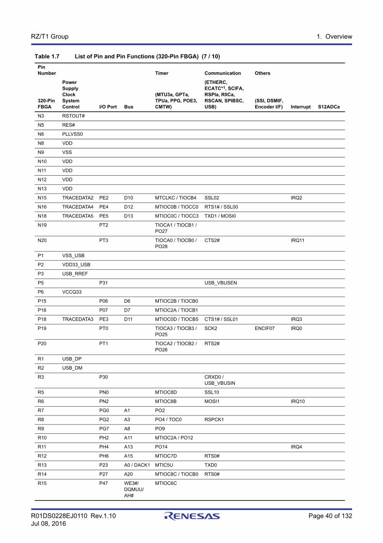
R01DS0228EJ0110 Rev.1.10 Page 40 of 132Jul 08, 2016
RZ/T1 Group 1. Overview
N3 RSTOUT#
N5 RES#
N6 PLLVSS0
N8 VDD
N9 VSS
N10 VDD
N11 VDD
N12 VDD
N13 VDD
N15 TRACEDATA2 PE2 D10 MTCLKC / TIOCB4 SSL02 IRQ2
N16 TRACEDATA4 PE4 D12 MTIOC0B / TIOCC0 RTS1# / SSL00
N18 TRACEDATA5 PE5 D13 MTIOC0C / TIOCC3 TXD1 / MOSI0
N19 PT2 TIOCA1 / TIOCB1 / PO27
N20 PT3 TIOCA0 / TIOCB0 / PO28
CTS2# IRQ11
P1 VSS_USB
P2 VDD33_USB
P3 USB_RREF
P5 P31 USB_VBUSEN
P6 VCCQ33
P15 P06 D6 MTIOC2B / TIOCB0
P16 P07 D7 MTIOC2A / TIOCB1
P18 TRACEDATA3 PE3 D11 MTIOC0D / TIOCB5 CTS1# / SSL01 IRQ3
P19 PT0 TIOCA3 / TIOCB3 / PO25
SCK2 ENCIF07 IRQ0
P20 PT1 TIOCA2 / TIOCB2 / PO26
RTS2#
R1 USB_DP
R2 USB_DM
R3 P30 CRXD0 / USB_VBUSIN
R5 PN0 MTIOC8D SSL10
R6 PN2 MTIOC8B MOSI1 IRQ10
R7 PG0 A1 PO2
R8 PG2 A3 PO4 / TOC0 RSPCK1
R9 PG7 A8 PO9
R10 PH2 A11 MTIOC2A / PO12
R11 PH4 A13 PO14 IRQ4
R12 PH6 A15 MTIOC7D RTS0#
R13 P23 A0 / DACK1 MTIC5U TXD0
R14 P27 A20 MTIOC8C / TIOCB0 RTS0#
R15 P47 WE3#/DQMUU/AH#
MTIOC6C
Table 1.7 List of Pin and Pin Functions (320-Pin FBGA) (7 / 10)
PinNumber
PowerSupplyClockSystemControl I/O Port Bus
Timer Communication Others
Interrupt S12ADCa320-PinFBGA
(MTU3a, GPTa, TPUa, PPG, POE3, CMTW)
(ETHERC, ECATC*1, SCIFA, RSPIa, RIICa, RSCAN, SPIBSC, USB)
(SSI, DSMIF,Encoder I/F)
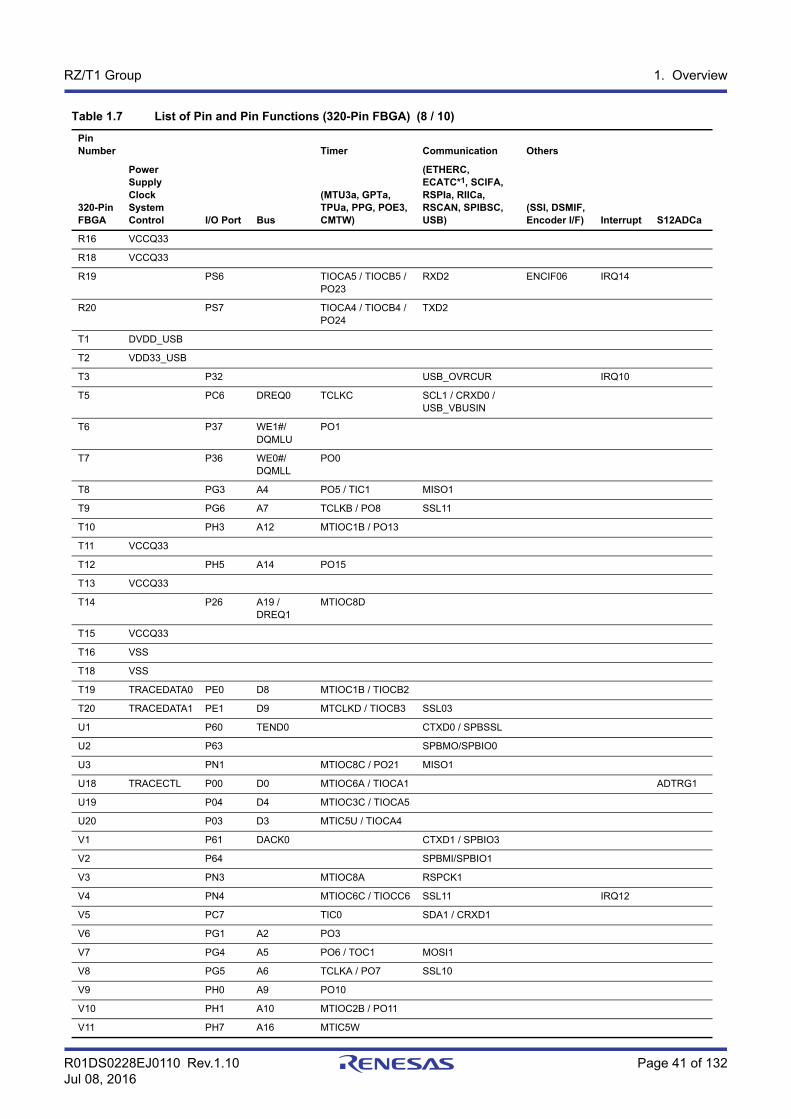
R01DS0228EJ0110 Rev.1.10 Page 41 of 132Jul 08, 2016
RZ/T1 Group 1. Overview
R16 VCCQ33
R18 VCCQ33
R19 PS6 TIOCA5 / TIOCB5 / PO23
RXD2 ENCIF06 IRQ14
R20 PS7 TIOCA4 / TIOCB4 / PO24
TXD2
T1 DVDD_USB
T2 VDD33_USB
T3 P32 USB_OVRCUR IRQ10
T5 PC6 DREQ0 TCLKC SCL1 / CRXD0 / USB_VBUSIN
T6 P37 WE1#/DQMLU
PO1
T7 P36 WE0#/DQMLL
PO0
T8 PG3 A4 PO5 / TIC1 MISO1
T9 PG6 A7 TCLKB / PO8 SSL11
T10 PH3 A12 MTIOC1B / PO13
T11 VCCQ33
T12 PH5 A14 PO15
T13 VCCQ33
T14 P26 A19 / DREQ1
MTIOC8D
T15 VCCQ33
T16 VSS
T18 VSS
T19 TRACEDATA0 PE0 D8 MTIOC1B / TIOCB2
T20 TRACEDATA1 PE1 D9 MTCLKD / TIOCB3 SSL03
U1 P60 TEND0 CTXD0 / SPBSSL
U2 P63 SPBMO/SPBIO0
U3 PN1 MTIOC8C / PO21 MISO1
U18 TRACECTL P00 D0 MTIOC6A / TIOCA1 ADTRG1
U19 P04 D4 MTIOC3C / TIOCA5
U20 P03 D3 MTIC5U / TIOCA4
V1 P61 DACK0 CTXD1 / SPBIO3
V2 P64 SPBMI/SPBIO1
V3 PN3 MTIOC8A RSPCK1
V4 PN4 MTIOC6C / TIOCC6 SSL11 IRQ12
V5 PC7 TIC0 SDA1 / CRXD1
V6 PG1 A2 PO3
V7 PG4 A5 PO6 / TOC1 MOSI1
V8 PG5 A6 TCLKA / PO7 SSL10
V9 PH0 A9 PO10
V10 PH1 A10 MTIOC2B / PO11
V11 PH7 A16 MTIC5W
Table 1.7 List of Pin and Pin Functions (320-Pin FBGA) (8 / 10)
PinNumber
PowerSupplyClockSystemControl I/O Port Bus
Timer Communication Others
Interrupt S12ADCa320-PinFBGA
(MTU3a, GPTa, TPUa, PPG, POE3, CMTW)
(ETHERC, ECATC*1, SCIFA, RSPIa, RIICa, RSCAN, SPIBSC, USB)
(SSI, DSMIF,Encoder I/F)
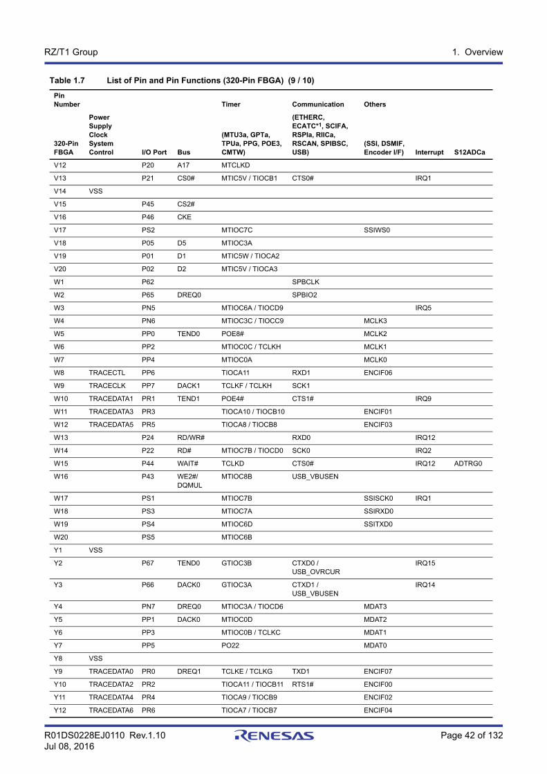
R01DS0228EJ0110 Rev.1.10 Page 42 of 132Jul 08, 2016
RZ/T1 Group 1. Overview
V12 P20 A17 MTCLKD
V13 P21 CS0# MTIC5V / TIOCB1 CTS0# IRQ1
V14 VSS
V15 P45 CS2#
V16 P46 CKE
V17 PS2 MTIOC7C SSIWS0
V18 P05 D5 MTIOC3A
V19 P01 D1 MTIC5W / TIOCA2
V20 P02 D2 MTIC5V / TIOCA3
W1 P62 SPBCLK
W2 P65 DREQ0 SPBIO2
W3 PN5 MTIOC6A / TIOCD9 IRQ5
W4 PN6 MTIOC3C / TIOCC9 MCLK3
W5 PP0 TEND0 POE8# MCLK2
W6 PP2 MTIOC0C / TCLKH MCLK1
W7 PP4 MTIOC0A MCLK0
W8 TRACECTL PP6 TIOCA11 RXD1 ENCIF06
W9 TRACECLK PP7 DACK1 TCLKF / TCLKH SCK1
W10 TRACEDATA1 PR1 TEND1 POE4# CTS1# IRQ9
W11 TRACEDATA3 PR3 TIOCA10 / TIOCB10 ENCIF01
W12 TRACEDATA5 PR5 TIOCA8 / TIOCB8 ENCIF03
W13 P24 RD/WR# RXD0 IRQ12
W14 P22 RD# MTIOC7B / TIOCD0 SCK0 IRQ2
W15 P44 WAIT# TCLKD CTS0# IRQ12 ADTRG0
W16 P43 WE2#/DQMUL
MTIOC8B USB_VBUSEN
W17 PS1 MTIOC7B SSISCK0 IRQ1
W18 PS3 MTIOC7A SSIRXD0
W19 PS4 MTIOC6D SSITXD0
W20 PS5 MTIOC6B
Y1 VSS
Y2 P67 TEND0 GTIOC3B CTXD0 / USB_OVRCUR
IRQ15
Y3 P66 DACK0 GTIOC3A CTXD1 / USB_VBUSEN
IRQ14
Y4 PN7 DREQ0 MTIOC3A / TIOCD6 MDAT3
Y5 PP1 DACK0 MTIOC0D MDAT2
Y6 PP3 MTIOC0B / TCLKC MDAT1
Y7 PP5 PO22 MDAT0
Y8 VSS
Y9 TRACEDATA0 PR0 DREQ1 TCLKE / TCLKG TXD1 ENCIF07
Y10 TRACEDATA2 PR2 TIOCA11 / TIOCB11 RTS1# ENCIF00
Y11 TRACEDATA4 PR4 TIOCA9 / TIOCB9 ENCIF02
Y12 TRACEDATA6 PR6 TIOCA7 / TIOCB7 ENCIF04
Table 1.7 List of Pin and Pin Functions (320-Pin FBGA) (9 / 10)
PinNumber
PowerSupplyClockSystemControl I/O Port Bus
Timer Communication Others
Interrupt S12ADCa320-PinFBGA
(MTU3a, GPTa, TPUa, PPG, POE3, CMTW)
(ETHERC, ECATC*1, SCIFA, RSPIa, RIICa, RSCAN, SPIBSC, USB)
(SSI, DSMIF,Encoder I/F)
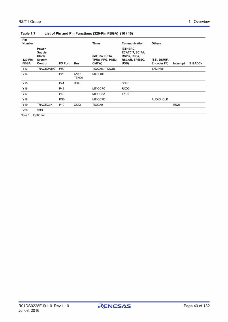
R01DS0228EJ0110 Rev.1.10 Page 43 of 132Jul 08, 2016
RZ/T1 Group 1. Overview
Note 1. Optional
Y13 TRACEDATA7 PR7 TIOCA6 / TIOCB6 ENCIF05
Y14 P25 A18 / TEND1
MTCLKC
Y15 P41 BS# SCK0
Y16 P42 MTIOC7C RXD0
Y17 P40 MTIOC8A TXD0
Y18 PS0 MTIOC7D AUDIO_CLK
Y19 TRACECLK P10 CKIO TIOCA0 IRQ0
Y20 VSS
Table 1.7 List of Pin and Pin Functions (320-Pin FBGA) (10 / 10)
PinNumber
PowerSupplyClockSystemControl I/O Port Bus
Timer Communication Others
Interrupt S12ADCa320-PinFBGA
(MTU3a, GPTa, TPUa, PPG, POE3, CMTW)
(ETHERC, ECATC*1, SCIFA, RSPIa, RIICa, RSCAN, SPIBSC, USB)
(SSI, DSMIF,Encoder I/F)
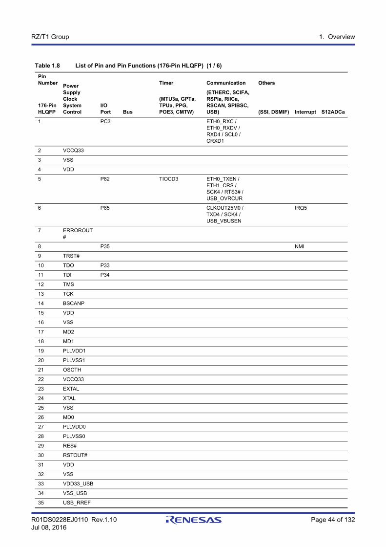
R01DS0228EJ0110 Rev.1.10 Page 44 of 132Jul 08, 2016
RZ/T1 Group 1. Overview
Table 1.8 List of Pin and Pin Functions (176-Pin HLQFP) (1 / 6)
PinNumber
PowerSupplyClockSystemControl
I/O Port Bus
Timer Communication Others
Interrupt S12ADCa176-PinHLQFP
(MTU3a, GPTa, TPUa, PPG, POE3, CMTW)
(ETHERC, SCIFA, RSPIa, RIICa, RSCAN, SPIBSC, USB) (SSI, DSMIF)
1 PC3 ETH0_RXC / ETH0_RXDV / RXD4 / SCL0 / CRXD1
2 VCCQ33
3 VSS
4 VDD
5 P82 TIOCD3 ETH0_TXEN / ETH1_CRS / SCK4 / RTS3# / USB_OVRCUR
6 P85 CLKOUT25M0 / TXD4 / SCK4 / USB_VBUSEN
IRQ5
7 ERROROUT#
8 P35 NMI
9 TRST#
10 TDO P33
11 TDI P34
12 TMS
13 TCK
14 BSCANP
15 VDD
16 VSS
17 MD2
18 MD1
19 PLLVDD1
20 PLLVSS1
21 OSCTH
22 VCCQ33
23 EXTAL
24 XTAL
25 VSS
26 MD0
27 PLLVDD0
28 PLLVSS0
29 RES#
30 RSTOUT#
31 VDD
32 VSS
33 VDD33_USB
34 VSS_USB
35 USB_RREF
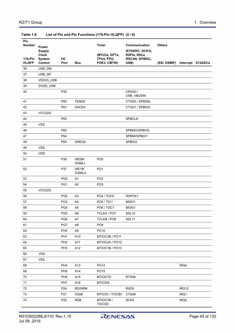
R01DS0228EJ0110 Rev.1.10 Page 45 of 132Jul 08, 2016
RZ/T1 Group 1. Overview
36 USB_DM
37 USB_DP
38 VDD33_USB
39 DVDD_USB
40 P30 CRXD0 / USB_VBUSIN
41 P60 TEND0 CTXD0 / SPBSSL
42 P61 DACK0 CTXD1 / SPBIO3
43 VCCQ33
44 P62 SPBCLK
45 VSS
46 P63 SPBMO/SPBIO0
47 P64 SPBMI/SPBIO1
48 P65 DREQ0 SPBIO2
49 VSS
50 VDD
51 P36 WE0#/DQMLL
PO0
52 P37 WE1#/DQMLU
PO1
53 PG0 A1 PO2
54 PG1 A2 PO3
55 VCCQ33
56 PG2 A3 PO4 / TOC0 RSPCK1
57 PG3 A4 PO5 / TIC1 MISO1
58 PG4 A5 PO6 / TOC1 MOSI1
59 PG5 A6 TCLKA / PO7 SSL10
60 PG6 A7 TCLKB / PO8 SSL11
61 PG7 A8 PO9
62 PH0 A9 PO10
63 PH1 A10 MTIOC2B / PO11
64 PH2 A11 MTIOC2A / PO12
65 PH3 A12 MTIOC1B / PO13
66 VDD
67 VSS
68 PH4 A13 PO14 IRQ4
69 PH5 A14 PO15
70 PH6 A15 MTIOC7D RTS0#
71 PH7 A16 MTIC5W
72 P24 RD/WR# RXD0 IRQ12
73 P21 CS0# MTIC5V / TIOCB1 CTS0# IRQ1
74 P22 RD# MTIOC7B / TIOCD0
SCK0 IRQ2
Table 1.8 List of Pin and Pin Functions (176-Pin HLQFP) (2 / 6)
PinNumber
PowerSupplyClockSystemControl
I/O Port Bus
Timer Communication Others
Interrupt S12ADCa176-PinHLQFP
(MTU3a, GPTa, TPUa, PPG, POE3, CMTW)
(ETHERC, SCIFA, RSPIa, RIICa, RSCAN, SPIBSC, USB) (SSI, DSMIF)
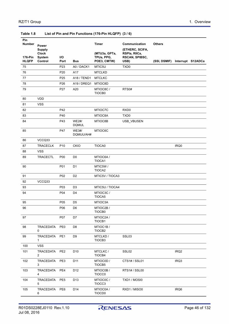
R01DS0228EJ0110 Rev.1.10 Page 46 of 132Jul 08, 2016
RZ/T1 Group 1. Overview
75 P23 A0 / DACK1 MTIC5U TXD0
76 P20 A17 MTCLKD
77 P25 A18 / TEND1 MTCLKC
78 P26 A19 / DREQ1 MTIOC8D
79 P27 A20 MTIOC8C / TIOCB0
RTS0#
80 VDD
81 VSS
82 P42 MTIOC7C RXD0
83 P40 MTIOC8A TXD0
84 P43 WE2#/DQMUL
MTIOC8B USB_VBUSEN
85 P47 WE3#/DQMUU/AH#
MTIOC6C
86 VCCQ33
87 TRACECLK P10 CKIO TIOCA0 IRQ0
88 VSS
89 TRACECTL P00 D0 MTIOC6A / TIOCA1
90 P01 D1 MTIC5W / TIOCA2
91 P02 D2 MTIC5V / TIOCA3
92 VCCQ33
93 P03 D3 MTIC5U / TIOCA4
94 P04 D4 MTIOC3C / TIOCA5
95 P05 D5 MTIOC3A
96 P06 D6 MTIOC2B / TIOCB0
97 P07 D7 MTIOC2A / TIOCB1
98 TRACEDATA0
PE0 D8 MTIOC1B / TIOCB2
99 TRACEDATA1
PE1 D9 MTCLKD / TIOCB3
SSL03
100 VSS
101 TRACEDATA2
PE2 D10 MTCLKC / TIOCB4
SSL02 IRQ2
102 TRACEDATA3
PE3 D11 MTIOC0D / TIOCB5
CTS1# / SSL01 IRQ3
103 TRACEDATA4
PE4 D12 MTIOC0B / TIOCC0
RTS1# / SSL00
104 TRACEDATA5
PE5 D13 MTIOC0C / TIOCC3
TXD1 / MOSI0
105 TRACEDATA6
PE6 D14 MTIOC0A / TIOCD0
RXD1 / MISO0 IRQ6
Table 1.8 List of Pin and Pin Functions (176-Pin HLQFP) (3 / 6)
PinNumber
PowerSupplyClockSystemControl
I/O Port Bus
Timer Communication Others
Interrupt S12ADCa176-PinHLQFP
(MTU3a, GPTa, TPUa, PPG, POE3, CMTW)
(ETHERC, SCIFA, RSPIa, RIICa, RSCAN, SPIBSC, USB) (SSI, DSMIF)
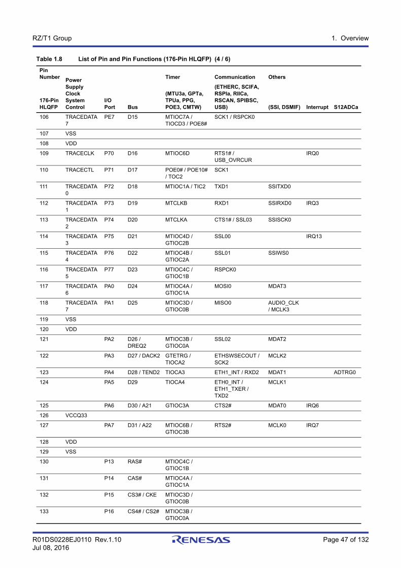
R01DS0228EJ0110 Rev.1.10 Page 47 of 132Jul 08, 2016
RZ/T1 Group 1. Overview
106 TRACEDATA7
PE7 D15 MTIOC7A / TIOCD3 / POE8#
SCK1 / RSPCK0
107 VSS
108 VDD
109 TRACECLK P70 D16 MTIOC6D RTS1# / USB_OVRCUR
IRQ0
110 TRACECTL P71 D17 POE0# / POE10# / TOC2
SCK1
111 TRACEDATA0
P72 D18 MTIOC1A / TIC2 TXD1 SSITXD0
112 TRACEDATA1
P73 D19 MTCLKB RXD1 SSIRXD0 IRQ3
113 TRACEDATA2
P74 D20 MTCLKA CTS1# / SSL03 SSISCK0
114 TRACEDATA3
P75 D21 MTIOC4D / GTIOC2B
SSL00 IRQ13
115 TRACEDATA4
P76 D22 MTIOC4B / GTIOC2A
SSL01 SSIWS0
116 TRACEDATA5
P77 D23 MTIOC4C / GTIOC1B
RSPCK0
117 TRACEDATA6
PA0 D24 MTIOC4A / GTIOC1A
MOSI0 MDAT3
118 TRACEDATA7
PA1 D25 MTIOC3D / GTIOC0B
MISO0 AUDIO_CLK / MCLK3
119 VSS
120 VDD
121 PA2 D26 / DREQ2
MTIOC3B / GTIOC0A
SSL02 MDAT2
122 PA3 D27 / DACK2 GTETRG / TIOCA2
ETHSWSECOUT / SCK2
MCLK2
123 PA4 D28 / TEND2 TIOCA3 ETH1_INT / RXD2 MDAT1 ADTRG0
124 PA5 D29 TIOCA4 ETH0_INT / ETH1_TXER / TXD2
MCLK1
125 PA6 D30 / A21 GTIOC3A CTS2# MDAT0 IRQ6
126 VCCQ33
127 PA7 D31 / A22 MTIOC6B / GTIOC3B
RTS2# MCLK0 IRQ7
128 VDD
129 VSS
130 P13 RAS# MTIOC4C / GTIOC1B
131 P14 CAS# MTIOC4A / GTIOC1A
132 P15 CS3# / CKE MTIOC3D / GTIOC0B
133 P16 CS4# / CS2# MTIOC3B / GTIOC0A
Table 1.8 List of Pin and Pin Functions (176-Pin HLQFP) (4 / 6)
PinNumber
PowerSupplyClockSystemControl
I/O Port Bus
Timer Communication Others
Interrupt S12ADCa176-PinHLQFP
(MTU3a, GPTa, TPUa, PPG, POE3, CMTW)
(ETHERC, SCIFA, RSPIa, RIICa, RSCAN, SPIBSC, USB) (SSI, DSMIF)
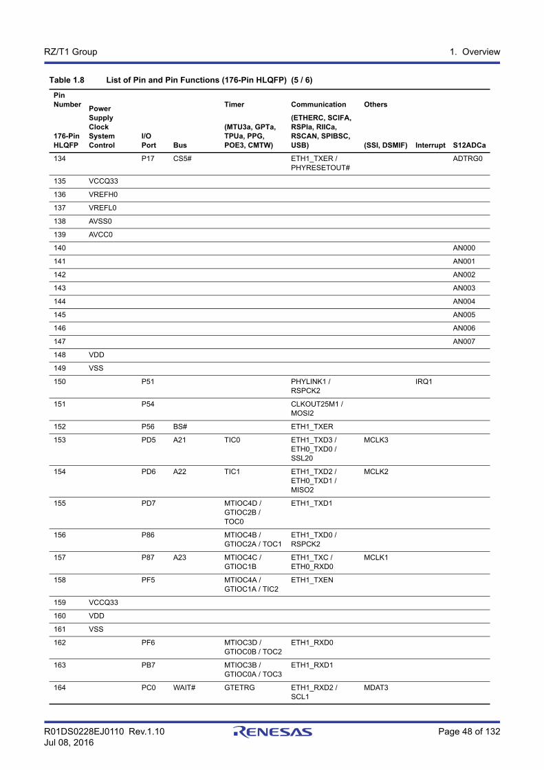
R01DS0228EJ0110 Rev.1.10 Page 48 of 132Jul 08, 2016
RZ/T1 Group 1. Overview
134 P17 CS5# ETH1_TXER / PHYRESETOUT#
ADTRG0
135 VCCQ33
136 VREFH0
137 VREFL0
138 AVSS0
139 AVCC0
140 AN000
141 AN001
142 AN002
143 AN003
144 AN004
145 AN005
146 AN006
147 AN007
148 VDD
149 VSS
150 P51 PHYLINK1 / RSPCK2
IRQ1
151 P54 CLKOUT25M1 / MOSI2
152 P56 BS# ETH1_TXER
153 PD5 A21 TIC0 ETH1_TXD3 / ETH0_TXD0 / SSL20
MCLK3
154 PD6 A22 TIC1 ETH1_TXD2 / ETH0_TXD1 / MISO2
MCLK2
155 PD7 MTIOC4D / GTIOC2B / TOC0
ETH1_TXD1
156 P86 MTIOC4B / GTIOC2A / TOC1
ETH1_TXD0 / RSPCK2
157 P87 A23 MTIOC4C / GTIOC1B
ETH1_TXC / ETH0_RXD0
MCLK1
158 PF5 MTIOC4A / GTIOC1A / TIC2
ETH1_TXEN
159 VCCQ33
160 VDD
161 VSS
162 PF6 MTIOC3D / GTIOC0B / TOC2
ETH1_RXD0
163 PB7 MTIOC3B / GTIOC0A / TOC3
ETH1_RXD1
164 PC0 WAIT# GTETRG ETH1_RXD2 / SCL1
MDAT3
Table 1.8 List of Pin and Pin Functions (176-Pin HLQFP) (5 / 6)
PinNumber
PowerSupplyClockSystemControl
I/O Port Bus
Timer Communication Others
Interrupt S12ADCa176-PinHLQFP
(MTU3a, GPTa, TPUa, PPG, POE3, CMTW)
(ETHERC, SCIFA, RSPIa, RIICa, RSCAN, SPIBSC, USB) (SSI, DSMIF)
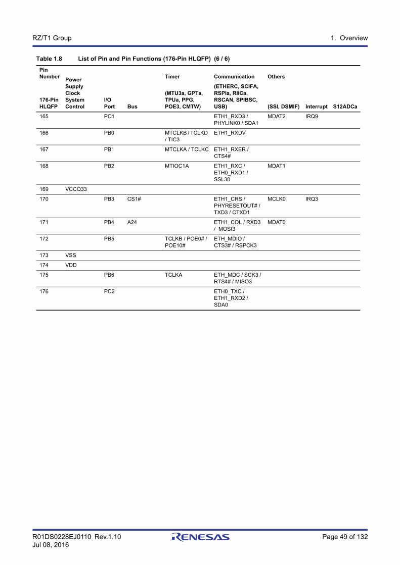
R01DS0228EJ0110 Rev.1.10 Page 49 of 132Jul 08, 2016
RZ/T1 Group 1. Overview
165 PC1 ETH1_RXD3 / PHYLINK0 / SDA1
MDAT2 IRQ9
166 PB0 MTCLKB / TCLKD / TIC3
ETH1_RXDV
167 PB1 MTCLKA / TCLKC ETH1_RXER / CTS4#
168 PB2 MTIOC1A ETH1_RXC / ETH0_RXD1 / SSL30
MDAT1
169 VCCQ33
170 PB3 CS1# ETH1_CRS / PHYRESETOUT# / TXD3 / CTXD1
MCLK0 IRQ3
171 PB4 A24 ETH1_COL / RXD3 / MOSI3
MDAT0
172 PB5 TCLKB / POE0# / POE10#
ETH_MDIO / CTS3# / RSPCK3
173 VSS
174 VDD
175 PB6 TCLKA ETH_MDC / SCK3 / RTS4# / MISO3
176 PC2 ETH0_TXC / ETH1_RXD2 / SDA0
Table 1.8 List of Pin and Pin Functions (176-Pin HLQFP) (6 / 6)
PinNumber
PowerSupplyClockSystemControl
I/O Port Bus
Timer Communication Others
Interrupt S12ADCa176-PinHLQFP
(MTU3a, GPTa, TPUa, PPG, POE3, CMTW)
(ETHERC, SCIFA, RSPIa, RIICa, RSCAN, SPIBSC, USB) (SSI, DSMIF)
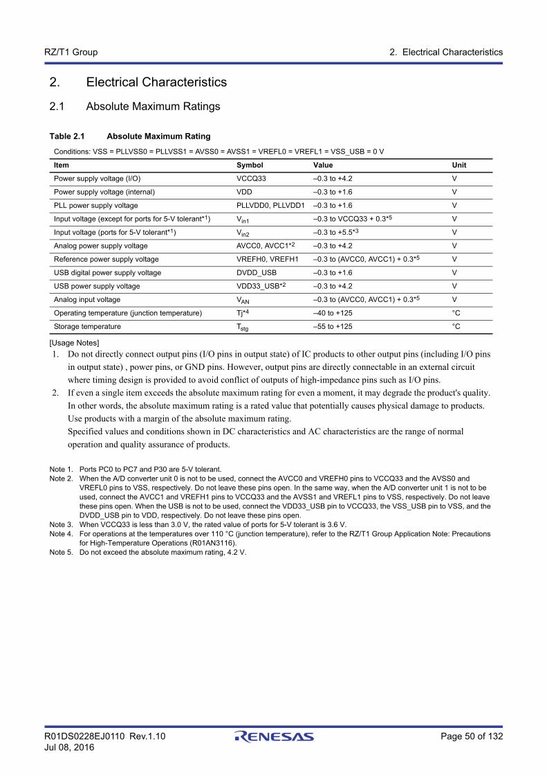
R01DS0228EJ0110 Rev.1.10 Page 50 of 132Jul 08, 2016
RZ/T1 Group 2. Electrical Characteristics
2. Electrical Characteristics
2.1 Absolute Maximum Ratings
[Usage Notes]
1. Do not directly connect output pins (I/O pins in output state) of IC products to other output pins (including I/O pins
in output state) , power pins, or GND pins. However, output pins are directly connectable in an external circuit
where timing design is provided to avoid conflict of outputs of high-impedance pins such as I/O pins.
2. If even a single item exceeds the absolute maximum rating for even a moment, it may degrade the product's quality.
In other words, the absolute maximum rating is a rated value that potentially causes physical damage to products.
Use products with a margin of the absolute maximum rating.
Specified values and conditions shown in DC characteristics and AC characteristics are the range of normal
operation and quality assurance of products.
Note 1. Ports PC0 to PC7 and P30 are 5-V tolerant.Note 2. When the A/D converter unit 0 is not to be used, connect the AVCC0 and VREFH0 pins to VCCQ33 and the AVSS0 and
VREFL0 pins to VSS, respectively. Do not leave these pins open. In the same way, when the A/D converter unit 1 is not to be used, connect the AVCC1 and VREFH1 pins to VCCQ33 and the AVSS1 and VREFL1 pins to VSS, respectively. Do not leave these pins open. When the USB is not to be used, connect the VDD33_USB pin to VCCQ33, the VSS_USB pin to VSS, and the DVDD_USB pin to VDD, respectively. Do not leave these pins open.
Note 3. When VCCQ33 is less than 3.0 V, the rated value of ports for 5-V tolerant is 3.6 V.Note 4. For operations at the temperatures over 110 °C (junction temperature), refer to the RZ/T1 Group Application Note: Precautions
for High-Temperature Operations (R01AN3116).Note 5. Do not exceed the absolute maximum rating, 4.2 V.
Table 2.1 Absolute Maximum Rating
Conditions: VSS = PLLVSS0 = PLLVSS1 = AVSS0 = AVSS1 = VREFL0 = VREFL1 = VSS_USB = 0 V
Item Symbol Value Unit
Power supply voltage (I/O) VCCQ33 –0.3 to +4.2 V
Power supply voltage (internal) VDD –0.3 to +1.6 V
PLL power supply voltage PLLVDD0, PLLVDD1 –0.3 to +1.6 V
Input voltage (except for ports for 5-V tolerant*1) Vin1 –0.3 to VCCQ33 + 0.3*5 V
Input voltage (ports for 5-V tolerant*1) Vin2 –0.3 to +5.5*3 V
Analog power supply voltage AVCC0, AVCC1*2 –0.3 to +4.2 V
Reference power supply voltage VREFH0, VREFH1 –0.3 to (AVCC0, AVCC1) + 0.3*5 V
USB digital power supply voltage DVDD_USB –0.3 to +1.6 V
USB power supply voltage VDD33_USB*2 –0.3 to +4.2 V
Analog input voltage VAN –0.3 to (AVCC0, AVCC1) + 0.3*5 V
Operating temperature (junction temperature) Tj*4 –40 to +125 °C
Storage temperature Tstg –55 to +125 °C

R01DS0228EJ0110 Rev.1.10 Page 51 of 132Jul 08, 2016
RZ/T1 Group 2. Electrical Characteristics
2.2 Power On/Off Sequence
Turn on and off each power supply voltage according to the procedure shown in the figure below.
When turning on the power, be sure to fix TRST# pins and RES# pins to the low level. Otherwise, initialization is not
performed successfully.
Note 1. Turn on all power supply voltages and reset signals with a monotonic increase and turn off with a monotonic decrease.
Note 2. Do not apply a negative voltage to power supply voltages.Note 3. Before turning on the power, be sure to make reset pins (TRST# and RES#) active (low). Otherwise, inputs and
outputs on the pins may be unstable. If this may also be a problem when turning off the power, make reset pins (TRST# and RES#) active (low.)
Note: If the power on/off sequence is not met (out of operation guarantee range), the pin input state and output state may be undefined.
Figure 2.1 Power On/Off Sequence
Powered down Power up sequence Active Power down sequence
Powered down (reverse order)
(1)Trisepwr
VDD
1.2 V for Digital
(1)Trisepwr
DVDD_USB (2)Tdly12
1.2 V for USB
PLLVDD0,PLLVDD1
(2)Tdly12
1.2 V for PLL
(1)Trisepwr
(3)Tdlyana33
AVCC0,AVCC1
VREFH0,VREFH1
3.3 V for Analog (1)Trisepwr
(4)Tdlyusb33
VDD33_USB 3.3 V for USB
(1)Trisepwr
(5)Tdly33
VCCQ33 3.3 V for I/O
XTAL/EXTAL
(6)Tdlyreset
RES#
TRST#
Oscillation
(7)Trisereset
(8)Tdlypwr
(8)Tdlypwr
(8)Tdlypwr
Timing
No. Item
Value
min typ max
(1) Trisepwr 100 us ― 50 ms
(2) Tdly12 0 ms ― 100 ms
(3) Tdlyana33 0 ms 100 ms
(4) Tdlyusb33 0 ms 100 ms
(5) Tdly33 0 ms 100 ms
(6) Tdlyreset 10 ms ― ―
(7) Trisereset ― ― 150 μs
(8) Tdlypwr 0 ms ― ―
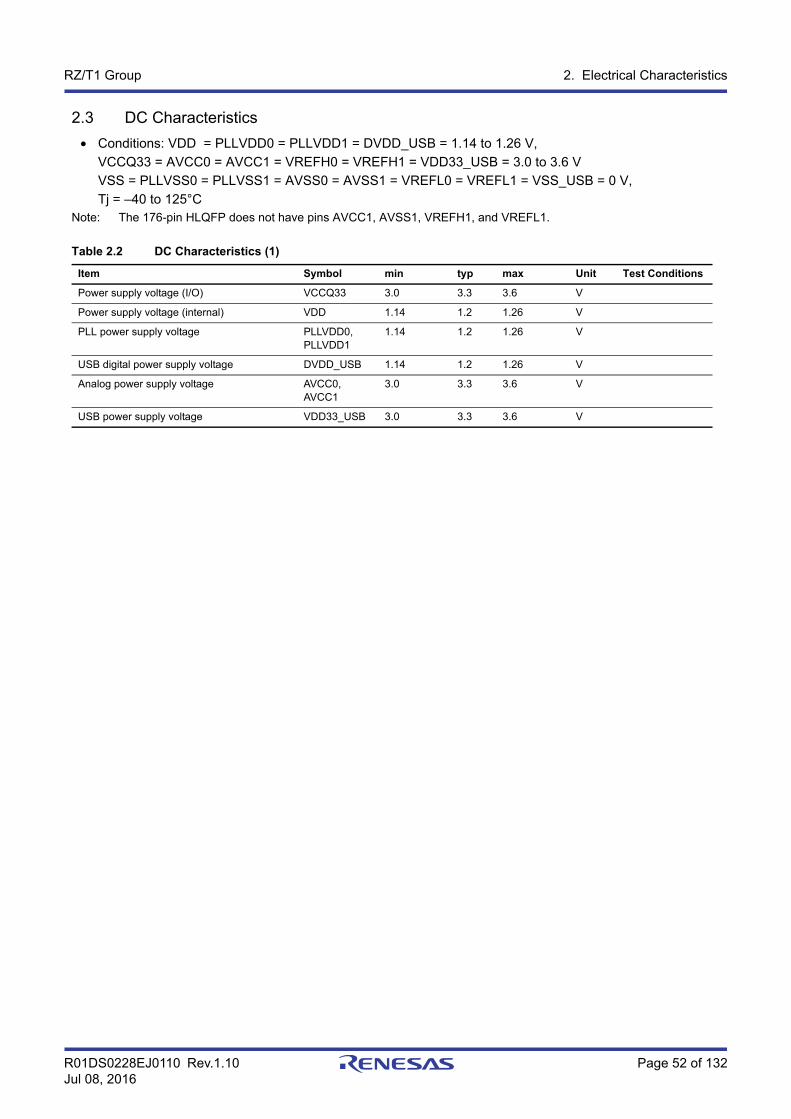
R01DS0228EJ0110 Rev.1.10 Page 52 of 132Jul 08, 2016
RZ/T1 Group 2. Electrical Characteristics
2.3 DC Characteristics
• Conditions: VDD = PLLVDD0 = PLLVDD1 = DVDD_USB = 1.14 to 1.26 V,
VCCQ33 = AVCC0 = AVCC1 = VREFH0 = VREFH1 = VDD33_USB = 3.0 to 3.6 V
VSS = PLLVSS0 = PLLVSS1 = AVSS0 = AVSS1 = VREFL0 = VREFL1 = VSS_USB = 0 V,
Tj = –40 to 125°CNote: The 176-pin HLQFP does not have pins AVCC1, AVSS1, VREFH1, and VREFL1.
Table 2.2 DC Characteristics (1)
Item Symbol min typ max Unit Test Conditions
Power supply voltage (I/O) VCCQ33 3.0 3.3 3.6 V
Power supply voltage (internal) VDD 1.14 1.2 1.26 V
PLL power supply voltage PLLVDD0, PLLVDD1
1.14 1.2 1.26 V
USB digital power supply voltage DVDD_USB 1.14 1.2 1.26 V
Analog power supply voltage AVCC0, AVCC1
3.0 3.3 3.6 V
USB power supply voltage VDD33_USB 3.0 3.3 3.6 V
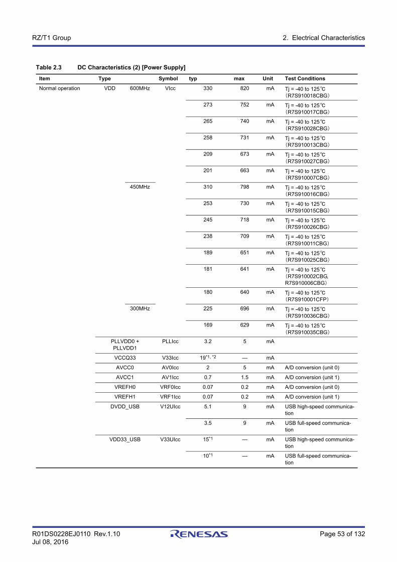
R01DS0228EJ0110 Rev.1.10 Page 53 of 132Jul 08, 2016
RZ/T1 Group 2. Electrical Characteristics
Table 2.3 DC Characteristics (2) [Power Supply]
Item Type Symbol typ max Unit Test Conditions
Normal operation VDD 600MHz VIcc 330 820 mA Tj = -40 to 125(R7S910018CBG)
273 752 mA Tj = -40 to 125(R7S910017CBG)
265 740 mA Tj = -40 to 125(R7S910028CBG)
258 731 mA Tj = -40 to 125(R7S910013CBG)
209 673 mA Tj = -40 to 125(R7S910027CBG)
201 663 mA Tj = -40 to 125(R7S910007CBG)
450MHz 310 798 mA Tj = -40 to 125(R7S910016CBG)
253 730 mA Tj = -40 to 125(R7S910015CBG)
245 718 mA Tj = -40 to 125(R7S910026CBG)
238 709 mA Tj = -40 to 125(R7S910011CBG)
189 651 mA Tj = -40 to 125(R7S910025CBG)
181 641 mA Tj = -40 to 125(R7S910002CBG, R7S910006CBG)
180 640 mA Tj = -40 to 125(R7S910001CFP)
300MHz 225 696 mA Tj = -40 to 125(R7S910036CBG)
169 629 mA Tj = -40 to 125(R7S910035CBG)
PLLVDD0 + PLLVDD1
PLLIcc 3.2 5 mA
VCCQ33 V33Icc 19*1, *2 — mA
AVCC0 AV0Icc 2 5 mA A/D conversion (unit 0)
AVCC1 AV1Icc 0.7 1.5 mA A/D conversion (unit 1)
VREFH0 VRF0Icc 0.07 0.2 mA A/D conversion (unit 0)
VREFH1 VRF1Icc 0.07 0.2 mA A/D conversion (unit 1)
DVDD_USB V12UIcc 5.1 9 mA USB high-speed communica-tion
3.5 9 mA USB full-speed communica-tion
VDD33_USB V33UIcc 15*1 — mA USB high-speed communica-tion
10*1 — mA USB full-speed communica-tion
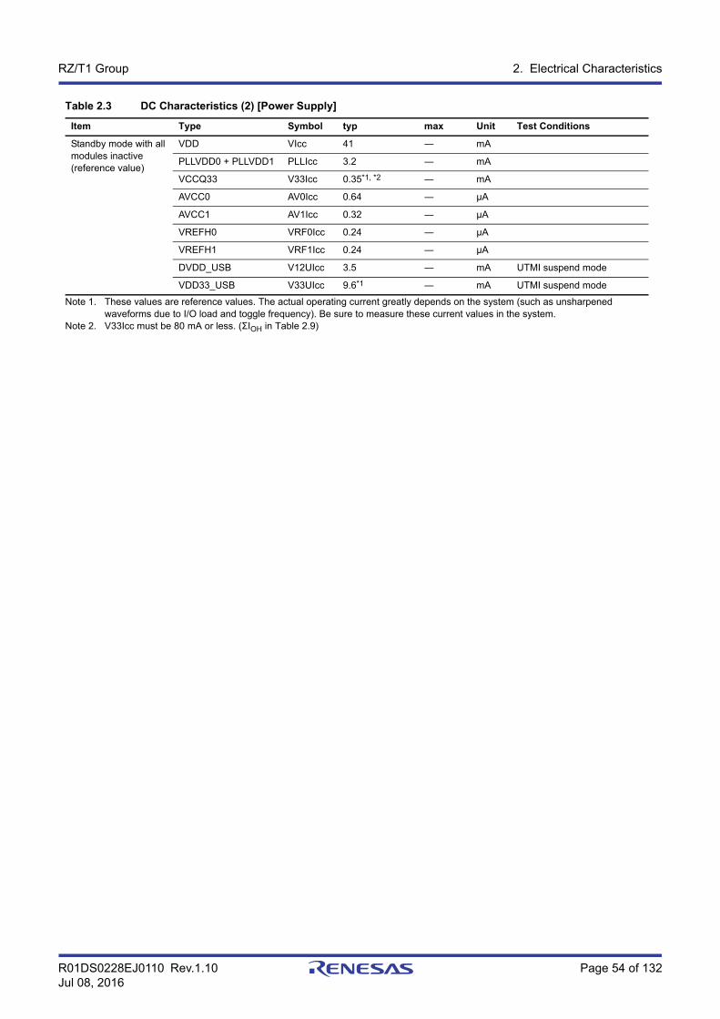
R01DS0228EJ0110 Rev.1.10 Page 54 of 132Jul 08, 2016
RZ/T1 Group 2. Electrical Characteristics
Note 1. These values are reference values. The actual operating current greatly depends on the system (such as unsharpened waveforms due to I/O load and toggle frequency). Be sure to measure these current values in the system.
Note 2. V33Icc must be 80 mA or less. (ΣIOH in Table 2.9)
Standby mode with all modules inactive(reference value)
VDD VIcc 41 ― mA
PLLVDD0 + PLLVDD1 PLLIcc 3.2 ― mA
VCCQ33 V33Icc 0.35*1, *2 ― mA
AVCC0 AV0Icc 0.64 ― μA
AVCC1 AV1Icc 0.32 ― μA
VREFH0 VRF0Icc 0.24 ― μA
VREFH1 VRF1Icc 0.24 ― μA
DVDD_USB V12UIcc 3.5 ― mA UTMI suspend mode
VDD33_USB V33UIcc 9.6*1 ― mA UTMI suspend mode
Table 2.3 DC Characteristics (2) [Power Supply]
Item Type Symbol typ max Unit Test Conditions
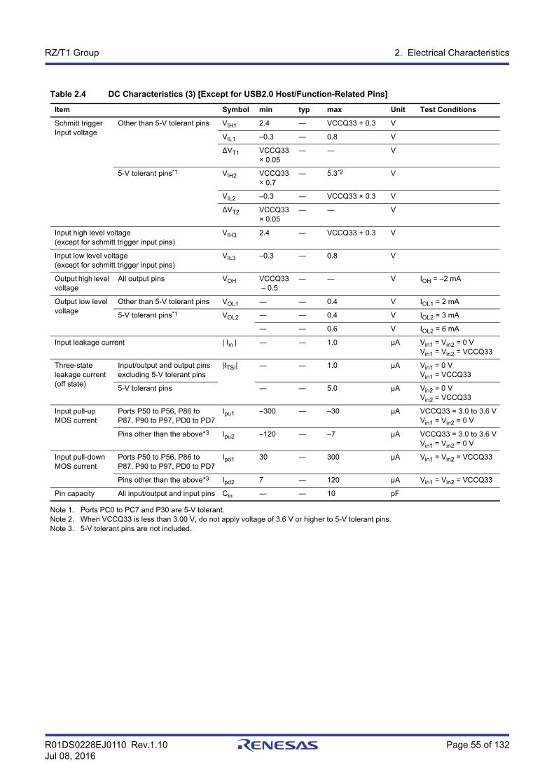
R01DS0228EJ0110 Rev.1.10 Page 55 of 132Jul 08, 2016
RZ/T1 Group 2. Electrical Characteristics
Note 1. Ports PC0 to PC7 and P30 are 5-V tolerant.Note 2. When VCCQ33 is less than 3.00 V, do not apply voltage of 3.6 V or higher to 5-V tolerant pins.Note 3. 5-V tolerant pins are not included.
Table 2.4 DC Characteristics (3) [Except for USB2.0 Host/Function-Related Pins]
Item Symbol min typ max Unit Test Conditions
Schmitt trigger Input voltage
Other than 5-V tolerant pins VIH1 2.4 ― VCCQ33 + 0.3 V
VIL1 –0.3 ― 0.8 V
∆VT1 VCCQ33 × 0.05
― ― V
5-V tolerant pins*1 VIH2 VCCQ33 × 0.7
― 5.3*2 V
VIL2 –0.3 ― VCCQ33 × 0.3 V
∆VT2 VCCQ33 × 0.05
― ― V
Input high level voltage(except for schmitt trigger input pins)
VIH3 2.4 ― VCCQ33 + 0.3 V
Input low level voltage(except for schmitt trigger input pins)
VIL3 –0.3 ― 0.8 V
Output high level voltage
All output pins VOH VCCQ33 – 0.5
― ― V IOH = –2 mA
Output low level voltage
Other than 5-V tolerant pins VOL1 ― ― 0.4 V IOL1 = 2 mA
5-V tolerant pins*1 VOL2 ― ― 0.4 V IOL2 = 3 mA
― ― 0.6 V IOL2 = 6 mA
Input leakage current | Iin | ― ― 1.0 μA Vin1 = Vin2 = 0 VVin1 = Vin2 = VCCQ33
Three-state leakage current (off state)
Input/output and output pins excluding 5-V tolerant pins
|ITSI| ― ― 1.0 μA Vin1 = 0 VVin1 = VCCQ33
5-V tolerant pins ― ― 5.0 μA Vin2 = 0 VVin2 = VCCQ33
Input pull-up MOS current
Ports P50 to P56, P86 to P87, P90 to P97, PD0 to PD7
Ipu1 –300 ― –30 μA VCCQ33 = 3.0 to 3.6 VVin1 = Vin2 = 0 V
Pins other than the above*3 Ipu2 –120 ― –7 μA VCCQ33 = 3.0 to 3.6 VVin1 = Vin2 = 0 V
Input pull-down MOS current
Ports P50 to P56, P86 to P87, P90 to P97, PD0 to PD7
Ipd1 30 ― 300 μA Vin1 = Vin2 = VCCQ33
Pins other than the above*3 Ipd2 7 ― 120 μA Vin1 = Vin2 = VCCQ33
Pin capacity All input/output and input pins Cin ― ― 10 pF
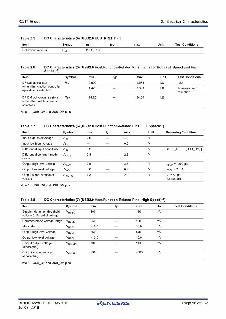
R01DS0228EJ0110 Rev.1.10 Page 56 of 132Jul 08, 2016
RZ/T1 Group 2. Electrical Characteristics
Note 1. USB_DP and USB_DM pins
Note 1. USB_DP and USB_DM pins
Note 1. USB_DP and USB_DM pins
Table 2.5 DC Characteristics (4) [USB2.0 USB_RREF Pin]
Item Symbol min typ max Unit Test Conditions
Reference resistor RREF 200Ω ±1%
Table 2.6 DC Characteristics (5) [USB2.0 Host/Function-Related Pins (Items for Both Full Speed and High Speed)*1]
Item Symbol min typ max Unit Test Conditions
DP pull-up resistor(when the function controller operation is selected)
RPU 0.900 ― 1.575 kΩ Idle
1.425 ― 3.090 kΩ Transmission/reception
DP/DM pull-down resistors(when the host function is selected)
RPD 14.25 ― 24.80 kΩ
Table 2.7 DC Characteristics (6) [USB2.0 Host/Function-Related Pins (Full Speed)*1]
Item Symbol min typ max Unit Measuring Condition
Input high level voltage VFSIH 2.0 ― ― V
Input low level voltage VFSIL ― ― 0.8 V
Differential input sensitivity VFSDI 0.2 ― ― V | (USB_DP) – (USB_DM) |
Differential common mode range
VFSCM 0.8 ― 2.5 V
Output high level voltage VFSOH 2.8 ― 3.6 V IFSOH = –200 μA
Output low level voltage VFSOL 0.0 ― 0.3 V IFSOL = 2 mA
Output signal crossover voltage
VFSCRS 1.3 ― 2.0 V CL = 50 pF(full-speed)
Table 2.8 DC Characteristics (7) [USB2.0 Host/Function-Related Pins (High Speed)*1]
Item Symbol min typ max Unit Test Conditions
Squelch detection threshold voltage (differential voltage)
VHSSQ 100 ― 150 mV
Common mode voltage range VHSCM –50 ― 500 mV
Idle state VHSOI –10.0 ― 10.0 mV
Output high level voltage VHSOH 360 ― 440 mV
Output low level voltage VHSOL –10.0 ― 10.0 mV
Chirp J output voltage (differential)
VCHIRPJ 700 ― 1100 mV
Chirp K output voltage (differential)
VCHIRPK –900 ― –500 mV

R01DS0228EJ0110 Rev.1.10 Page 57 of 132Jul 08, 2016
RZ/T1 Group 2. Electrical Characteristics
[Usage Notes] All output current values shall be within the values in Table 2.9 to ensure the reliability of this LSI.
Table 2.9 Permissible Output Currents
Item Symbol min typ max Unit
Permissible output low current(average value per pin)
Other than 5-V tolerant pins IOL1 ― ― 2.0 mA
5-V tolerant pins IOL2 ― ― 3.0 mA
Permissible output low current(maximum value per pin)
Other than 5-V tolerant pins IOL1 ― ― 4.0 mA
5-V tolerant pins IOL2 ― ― 6.0 mA
Permissible output low current (total) Total of all output pins ΣIOL ― ― 80 mA
Permissible output high current(average value per pin)
All output pins IOH ― ― –2.0 mA
Permissible output high current(maximum value per pin)
All output pins IOH ― ― –4.0 mA
Permissible output high current (total) Total of all output pins ΣIOH ― ― –80 mA
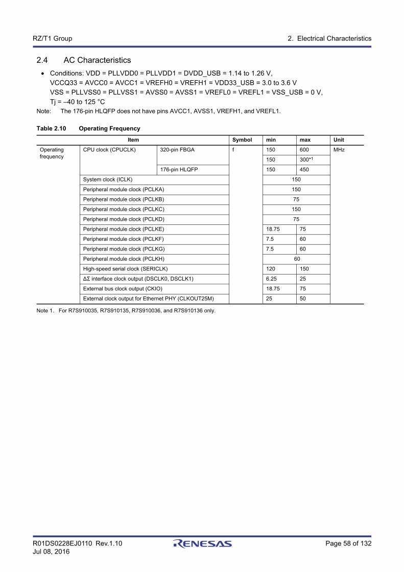
R01DS0228EJ0110 Rev.1.10 Page 58 of 132Jul 08, 2016
RZ/T1 Group 2. Electrical Characteristics
2.4 AC Characteristics
• Conditions: VDD = PLLVDD0 = PLLVDD1 = DVDD_USB = 1.14 to 1.26 V,
VCCQ33 = AVCC0 = AVCC1 = VREFH0 = VREFH1 = VDD33_USB = 3.0 to 3.6 V
VSS = PLLVSS0 = PLLVSS1 = AVSS0 = AVSS1 = VREFL0 = VREFL1 = VSS_USB = 0 V,
Tj = –40 to 125 °CNote: The 176-pin HLQFP does not have pins AVCC1, AVSS1, VREFH1, and VREFL1.
Note 1. For R7S910035, R7S910135, R7S910036, and R7S910136 only.
Table 2.10 Operating Frequency
Item Symbol min max Unit
Operating frequency
CPU clock (CPUCLK) 320-pin FBGA f 150 600 MHz
150 300*1
176-pin HLQFP 150 450
System clock (ICLK) 150
Peripheral module clock (PCLKA) 150
Peripheral module clock (PCLKB) 75
Peripheral module clock (PCLKC) 150
Peripheral module clock (PCLKD) 75
Peripheral module clock (PCLKE) 18.75 75
Peripheral module clock (PCLKF) 7.5 60
Peripheral module clock (PCLKG) 7.5 60
Peripheral module clock (PCLKH) 60
High-speed serial clock (SERICLK) 120 150
∆Σ interface clock output (DSCLK0, DSCLK1) 6.25 25
External bus clock output (CKIO) 18.75 75
External clock output for Ethernet PHY (CLKOUT25M) 25 50
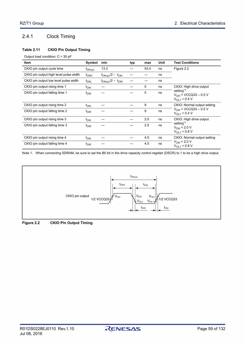
R01DS0228EJ0110 Rev.1.10 Page 59 of 132Jul 08, 2016
RZ/T1 Group 2. Electrical Characteristics
2.4.1 Clock Timing
Note 1. When connecting SDRAM, be sure to set the B0 bit in the drive capacity control register (DSCR) to 1 to be a high drive output.
Table 2.11 CKIO Pin Output Timing
Output load condition: C = 30 pF
Item Symbol min typ max Unit Test Conditions
CKIO pin output cycle time tCKcyc 13.3 ― 53.4 ns Figure 2.2
CKIO pin output high level pulse width tCKH tCKcyc/2 – tCKr ― ― ns
CKIO pin output low level pulse width tCKL tCKcyc/2 – tCKf ― ― ns
CKIO pin output rising time 1 tCKr ― ― 5 ns CKIO: High drive output setting*1
VOH = VCCQ33 – 0.5 VVOL1 = 0.4 V
CKIO pin output falling time 1 tCKf ― ― 5 ns
CKIO pin output rising time 2 tCKr ― ― 9 ns CKIO: Normal output settingVOH = VCCQ33 – 0.5 VVOL1 = 0.4 V
CKIO pin output falling time 2 tCKf ― ― 9 ns
CKIO pin output rising time 3 tCKr ― ― 2.5 ns CKIO: High drive output setting*1
VOH = 2.0 VVOL1 = 0.8 V
CKIO pin output falling time 3 tCKf ― ― 2.5 ns
CKIO pin output rising time 4 tCKr ― ― 4.5 ns CKIO: Normal output settingVOH = 2.0 VVOL1 = 0.8 V
CKIO pin output falling time 4 tCKf ― ― 4.5 ns
Figure 2.2 CKIO Pin Output Timing
tCKcyc
tCKf
CKIO pin output
tCKH tCKL
tCKr
1/2 VCCQ33 1/2 VCCQ33VOH VOH
VOL1
VOH
VOL1
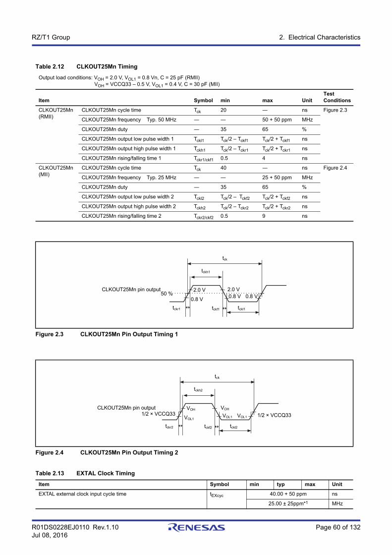
R01DS0228EJ0110 Rev.1.10 Page 60 of 132Jul 08, 2016
RZ/T1 Group 2. Electrical Characteristics
Table 2.12 CLKOUT25Mn Timing
Output load conditions: VOH = 2.0 V, VOL1 = 0.8 Vn, C = 25 pF (RMII) VOH = VCCQ33 – 0.5 V, VOL1 = 0.4 V, C = 30 pF (MII)
Item Symbol min max UnitTest Conditions
CLKOUT25Mn(RMII)
CLKOUT25Mn cycle time Tck 20 ― ns Figure 2.3
CLKOUT25Mn frequency Typ. 50 MHz ― ― 50 + 50 ppm MHz
CLKOUT25Mn duty ― 35 65 %
CLKOUT25Mn output low pulse width 1 Tckl1 Tck/2 – Tckf1 Tck/2 + Tckf1 ns
CLKOUT25Mn output high pulse width 1 Tckh1 Tck/2 – Tckr1 Tck/2 + Tckr1 ns
CLKOUT25Mn rising/falling time 1 Tckr1/ckf1 0.5 4 ns
CLKOUT25Mn(MII)
CLKOUT25Mn cycle time Tck 40 ― ns Figure 2.4
CLKOUT25Mn frequency Typ. 25 MHz ― ― 25 + 50 ppm MHz
CLKOUT25Mn duty ― 35 65 %
CLKOUT25Mn output low pulse width 2 Tckl2 Tck/2 – Tckf2 Tck/2 + Tckf2 ns
CLKOUT25Mn output high pulse width 2 Tckh2 Tck/2 – Tckr2 Tck/2 + Tckr2 ns
CLKOUT25Mn rising/falling time 2 Tckr2/ckf2 0.5 9 ns
Figure 2.3 CLKOUT25Mn Pin Output Timing 1
Figure 2.4 CLKOUT25Mn Pin Output Timing 2
Table 2.13 EXTAL Clock Timing
Item Symbol min typ max Unit
EXTAL external clock input cycle time tEXcyc 40.00 + 50 ppm ns
25.00 ± 25ppm*1 MHz
tck
CLKOUT25Mn pin output
tckh1
2.0 V 2.0 V0.8 V 0.8 V
tckl1
0.8 V
tckr1 tckf1
50 %
tck
CLKOUT25Mn pin output
tckh2
VOH VOH
VOL1 1/2 × VCCQ33VOL1
tckl2
VOL1
tckr2 tckf2
1/2 × VCCQ33
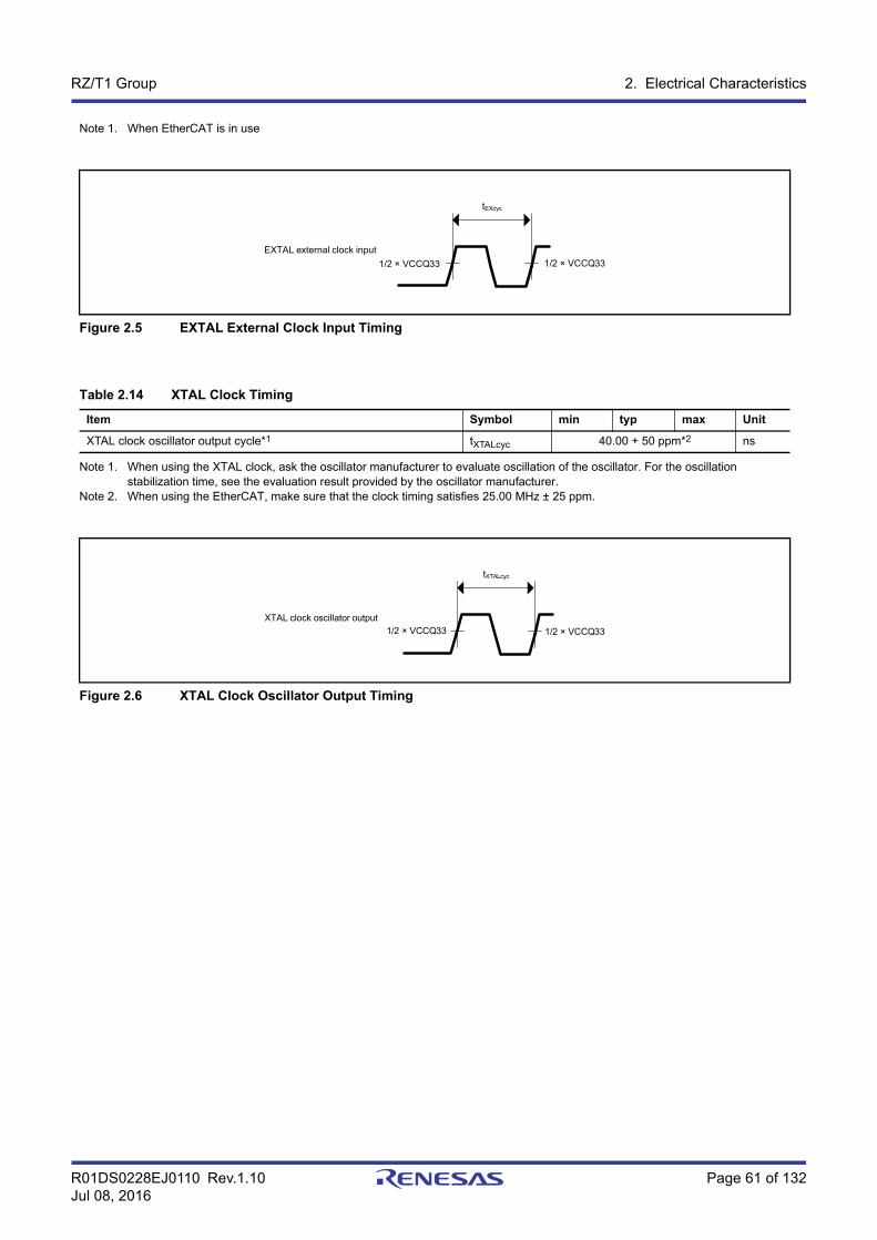
R01DS0228EJ0110 Rev.1.10 Page 61 of 132Jul 08, 2016
RZ/T1 Group 2. Electrical Characteristics
Note 1. When EtherCAT is in use
Note 1. When using the XTAL clock, ask the oscillator manufacturer to evaluate oscillation of the oscillator. For the oscillation stabilization time, see the evaluation result provided by the oscillator manufacturer.
Note 2. When using the EtherCAT, make sure that the clock timing satisfies 25.00 MHz ± 25 ppm.
Figure 2.5 EXTAL External Clock Input Timing
Table 2.14 XTAL Clock Timing
Item Symbol min typ max Unit
XTAL clock oscillator output cycle*1 tXTALcyc 40.00 + 50 ppm*2 ns
Figure 2.6 XTAL Clock Oscillator Output Timing
tEXcyc
1/2 × VCCQ33
EXTAL external clock input
1/2 × VCCQ33
tXTALcyc
1/2 × VCCQ33
XTAL clock oscillator output1/2 × VCCQ33
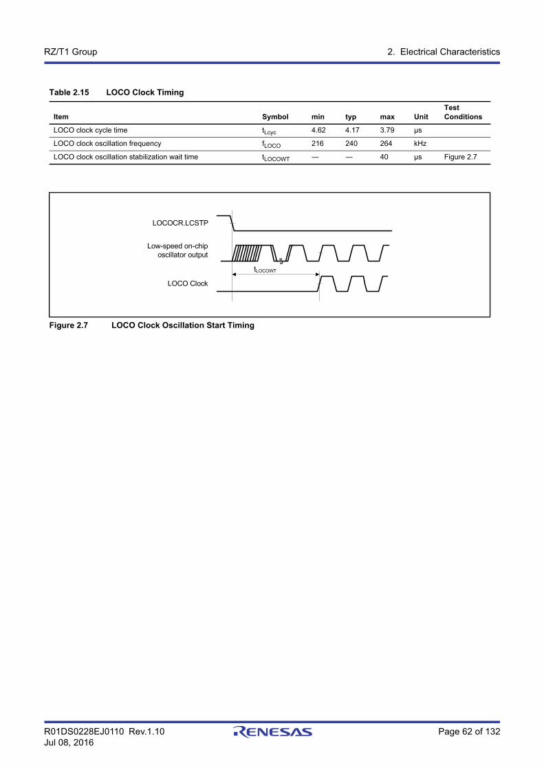
R01DS0228EJ0110 Rev.1.10 Page 62 of 132Jul 08, 2016
RZ/T1 Group 2. Electrical Characteristics
Table 2.15 LOCO Clock Timing
Item Symbol min typ max UnitTest Conditions
LOCO clock cycle time tLcyc 4.62 4.17 3.79 μs
LOCO clock oscillation frequency fLOCO 216 240 264 kHz
LOCO clock oscillation stabilization wait time tLOCOWT ― ― 40 μs Figure 2.7
Figure 2.7 LOCO Clock Oscillation Start Timing
LOCOCR.LCSTP
tLOCOWT
LOCO Clock
Low-speed on-chip oscillator output
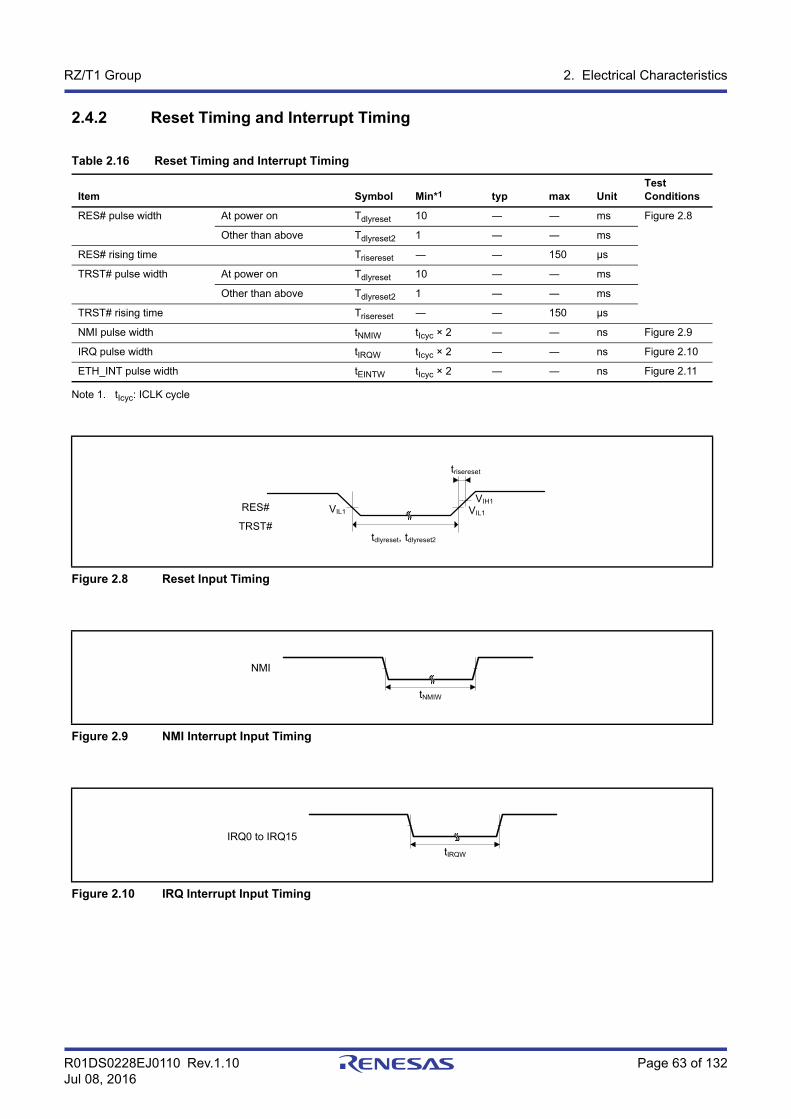
R01DS0228EJ0110 Rev.1.10 Page 63 of 132Jul 08, 2016
RZ/T1 Group 2. Electrical Characteristics
2.4.2 Reset Timing and Interrupt Timing
Note 1. tIcyc: ICLK cycle
Table 2.16 Reset Timing and Interrupt Timing
Item Symbol Min*1 typ max UnitTest Conditions
RES# pulse width At power on Tdlyreset 10 ― ― ms Figure 2.8
Other than above Tdlyreset2 1 ― ― ms
RES# rising time Trisereset ― ― 150 μs
TRST# pulse width At power on Tdlyreset 10 ― ― ms
Other than above Tdlyreset2 1 ― ― ms
TRST# rising time Trisereset ― ― 150 μs
NMI pulse width tNMIW tIcyc × 2 ― ― ns Figure 2.9
IRQ pulse width tIRQW tIcyc × 2 ― ― ns Figure 2.10
ETH_INT pulse width tEINTW tIcyc × 2 ― ― ns Figure 2.11
Figure 2.8 Reset Input Timing
Figure 2.9 NMI Interrupt Input Timing
Figure 2.10 IRQ Interrupt Input Timing
RES#
TRST#
VIL1 VIL1
VIH1
trisereset
tdlyreset, tdlyreset2
NMI
tNMIW
IRQ0 to IRQ15
tIRQW
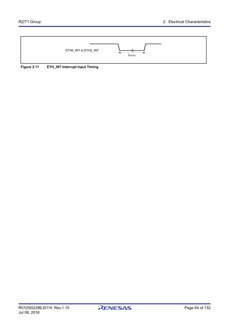
R01DS0228EJ0110 Rev.1.10 Page 64 of 132Jul 08, 2016
RZ/T1 Group 2. Electrical Characteristics
Figure 2.11 ETH_INT Interrupt Input Timing
ETH0_INT to ETH2_INT
tEINTW
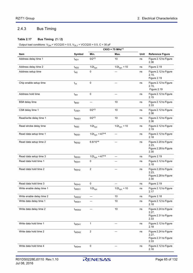
R01DS0228EJ0110 Rev.1.10 Page 65 of 132Jul 08, 2016
RZ/T1 Group 2. Electrical Characteristics
2.4.3 Bus Timing
Table 2.17 Bus Timing (1 / 2)
Output load conditions: VOH = VCCQ33 × 0.5, VOL1 = VCCQ33 × 0.5, C = 30 pF
Item Symbol
CKIO = 75 MHz*1
Unit Reference FigureMin. Max.
Address delay time 1 tAD1 0/2*3 10 ns Figure 2.12 to Figure 2.36
Address delay time 2 tAD2 1/2tcyc 1/2tcyc + 10 ns Figure 2.19
Address setup time tAS 0 ― ns Figure 2.12 to Figure 2.15,Figure 2.19
Chip enable setup time tcs 0 ― ns Figure 2.12 to Figure 2.15, Figure 2.19
Address hold time tAH 0 ― ns Figure 2.12 to Figure 2.15
BS# delay time tBSD ― 10 ns Figure 2.12 to Figure 2.33
CS# delay time 1 tCSD1 0/2*3 10 ns Figure 2.12 to Figure 2.36
Read/write delay time 1 tRWD1 0/2*3 10 ns Figure 2.12 to Figure 2.36
Read strobe delay time tRSD 1/2tcyc 1/2tcyc + 10 ns Figure 2.12 to Figure 2.19
Read data setup time 1 tRDS1 1/2tcyc + 4/7*4 ― ns Figure 2.12 to Figure 2.18
Read data setup time 2 tRDS2 6.6/10*4 ― ns Figure 2.20 to Figure 2.23,Figure 2.28 to Figure 2.30
Read data setup time 3 tRDS3 1/2tcyc + 4/7*4 ― ns Figure 2.19
Read data hold time 1 tRDH1 0 ― ns Figure 2.12 to Figure 2.18
Read data hold time 2 tRDH2 2 ― ns Figure 2.20 to Figure 2.23,Figure 2.28 to Figure 2.30
Read data hold time 3 tRDH3 0 ― ns Figure 2.19
Write enable delay time 1 tWED1 1/2tcyc 1/2tcyc + 10 ns Figure 2.12 to Figure 2.17
Write enable delay time 2 tWED2 ― 10 ns Figure 2.18
Write data delay time 1 tWDD1 ― 10 ns Figure 2.12 to Figure 2.18
Write data delay time 2 tWDD2 ― 10 ns Figure 2.24 to Figure 2.27,Figure 2.31 to Figure 2.33
Write data hold time 1 tWDH1 1 ― ns Figure 2.12 to Figure 2.18
Write data hold time 2 tWDH2 2 ― ns Figure 2.24 to Figure 2.27,Figure 2.31 to Figure 2.33
Write data hold time 4 tWDH4 0 ― ns Figure 2.12 to Figure 2.16
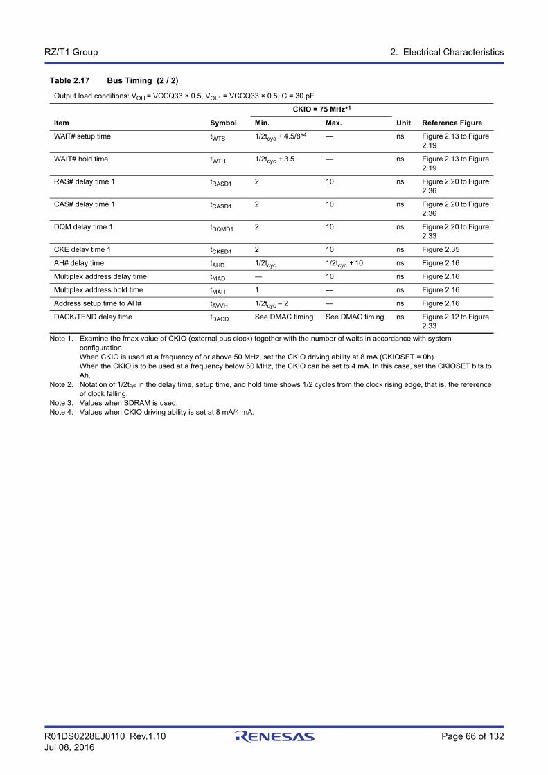
R01DS0228EJ0110 Rev.1.10 Page 66 of 132Jul 08, 2016
RZ/T1 Group 2. Electrical Characteristics
Note 1. Examine the fmax value of CKIO (external bus clock) together with the number of waits in accordance with system configuration.When CKIO is used at a frequency of or above 50 MHz, set the CKIO driving ability at 8 mA (CKIOSET = 0h).When the CKIO is to be used at a frequency below 50 MHz, the CKIO can be set to 4 mA. In this case, set the CKIOSET bits to Ah.
Note 2. Notation of 1/2tcyc in the delay time, setup time, and hold time shows 1/2 cycles from the clock rising edge, that is, the reference of clock falling.
Note 3. Values when SDRAM is used.Note 4. Values when CKIO driving ability is set at 8 mA/4 mA.
WAIT# setup time tWTS 1/2tcyc + 4.5/8*4 ― ns Figure 2.13 to Figure 2.19
WAIT# hold time tWTH 1/2tcyc + 3.5 ― ns Figure 2.13 to Figure 2.19
RAS# delay time 1 tRASD1 2 10 ns Figure 2.20 to Figure 2.36
CAS# delay time 1 tCASD1 2 10 ns Figure 2.20 to Figure 2.36
DQM delay time 1 tDQMD1 2 10 ns Figure 2.20 to Figure 2.33
CKE delay time 1 tCKED1 2 10 ns Figure 2.35
AH# delay time tAHD 1/2tcyc 1/2tcyc + 10 ns Figure 2.16
Multiplex address delay time tMAD ― 10 ns Figure 2.16
Multiplex address hold time tMAH 1 ― ns Figure 2.16
Address setup time to AH# tAVVH 1/2tcyc – 2 ― ns Figure 2.16
DACK/TEND delay time tDACD See DMAC timing See DMAC timing ns Figure 2.12 to Figure 2.33
Table 2.17 Bus Timing (2 / 2)
Output load conditions: VOH = VCCQ33 × 0.5, VOL1 = VCCQ33 × 0.5, C = 30 pF
Item Symbol
CKIO = 75 MHz*1
Unit Reference FigureMin. Max.
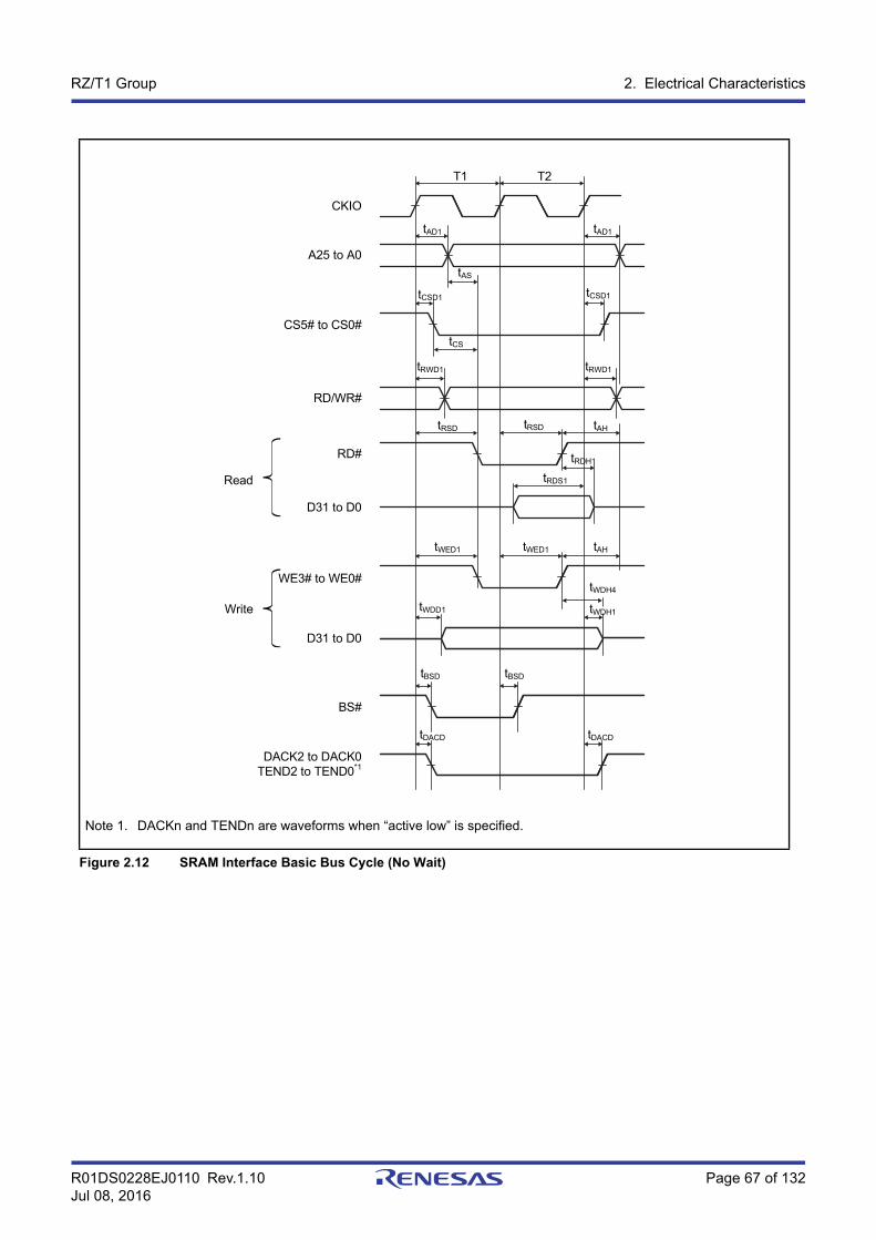
R01DS0228EJ0110 Rev.1.10 Page 67 of 132Jul 08, 2016
RZ/T1 Group 2. Electrical Characteristics
Note 1. DACKn and TENDn are waveforms when “active low” is specified.
Figure 2.12 SRAM Interface Basic Bus Cycle (No Wait)
T1 T2
tAD1 tAD1
tAS
tCSD1 tCSD1
tCS
tRWD1 tRWD1
tRSD tRSD tAH
tRDH1
tRDS1
tWED1 tWED1 tAH
tWDH4
tWDH1tWDD1
tBSD tBSD
tDACD tDACD
CKIO
A25 to A0
CS5# to CS0#
RD/WR#
RD#
D31 to D0
WE3# to WE0#
D31 to D0
BS#
DACK2 to DACK0TEND2 to TEND0*1
Read
Write
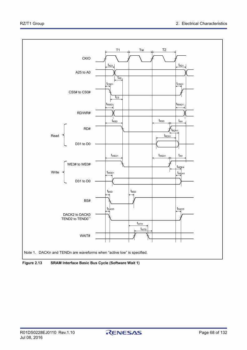
R01DS0228EJ0110 Rev.1.10 Page 68 of 132Jul 08, 2016
RZ/T1 Group 2. Electrical Characteristics
Note 1. DACKn and TENDn are waveforms when “active low” is specified.
Figure 2.13 SRAM Interface Basic Bus Cycle (Software Wait 1)
T1 Tw
tAD1 tAD1
tAS
tCSD1 tCSD1
tCS
tRWD1 tRWD1
tRSD tRSD tAH
tRDH1
tRDS1
tWED1 tWED1 tAH
tWDH4
tWDH1tWDD1
tBSD tBSD
tDACD tDACD
CKIO
A25 to A0
CS5# to CS0#
RD/WR#
RD#
D31 to D0
WE3# to WE0#
D31 to D0
BS#
DACK2 to DACK0TEND2 to TEND0*1
T2
WAIT#
tWTH
tWTS
Read
Write
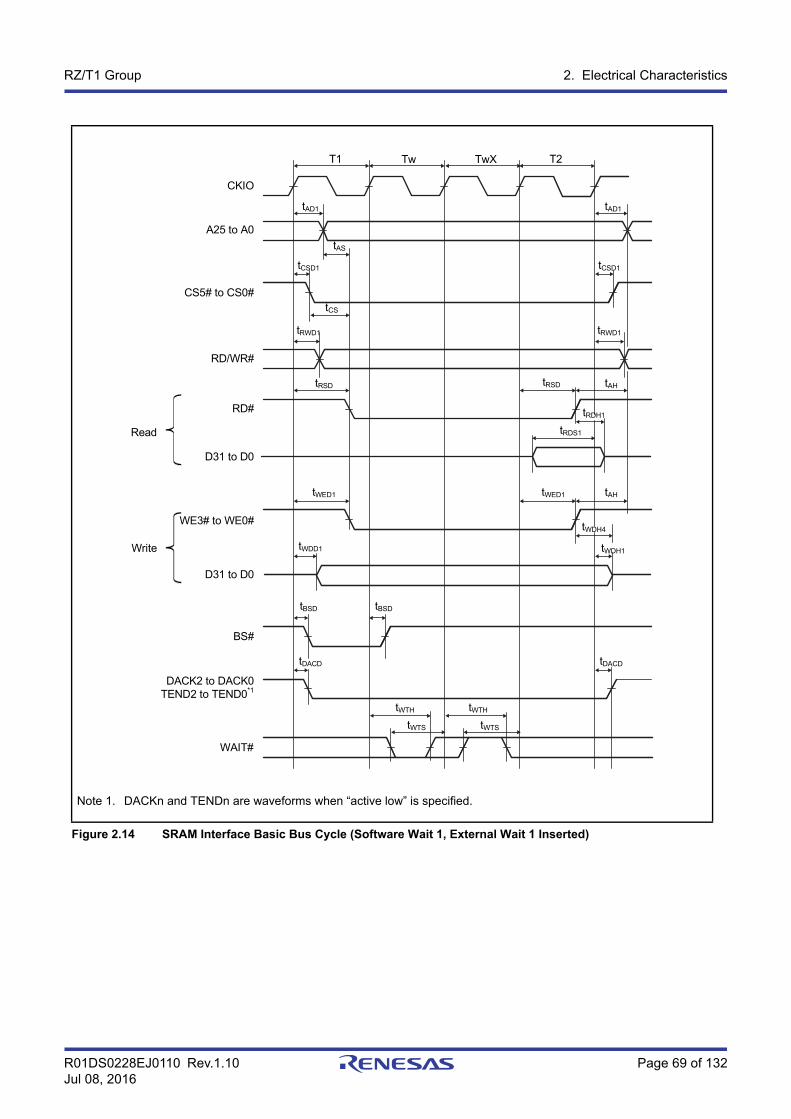
R01DS0228EJ0110 Rev.1.10 Page 69 of 132Jul 08, 2016
RZ/T1 Group 2. Electrical Characteristics
Note 1. DACKn and TENDn are waveforms when “active low” is specified.
Figure 2.14 SRAM Interface Basic Bus Cycle (Software Wait 1, External Wait 1 Inserted)
T1 T2
tAD1 tAD1
tAS
tCSD1 tCSD1
tCS
tRWD1 tRWD1
tRSD tRSD tAH
tRDS1
tWED1 tWED1 tAH
tWDH1tWDD1
tBSD tBSD
tDACD tDACD
CKIO
A25 to A0
CS5# to CS0#
RD/WR#
RD#
D31 to D0
WE3# to WE0#
D31 to D0
BS#
DACK2 to DACK0TEND2 to TEND0*1
Read
Write
WAIT#
Tw TwX
tRDH1
tWDH4
tWTH tWTH
tWTS tWTS
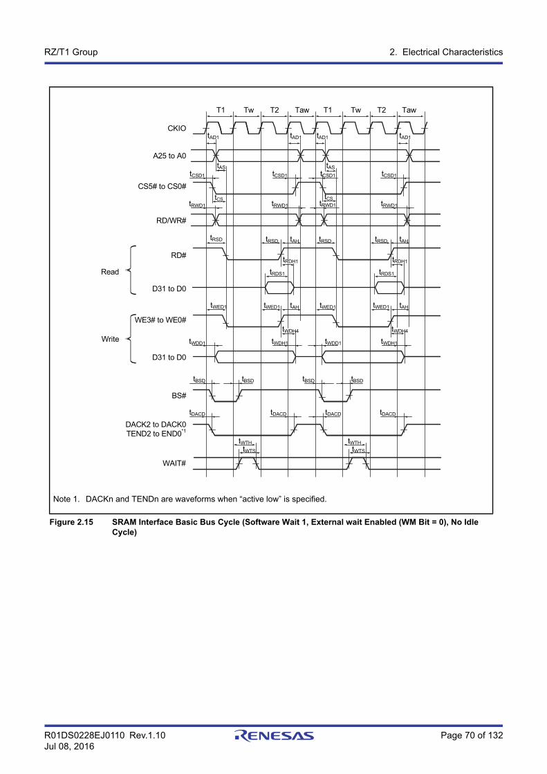
R01DS0228EJ0110 Rev.1.10 Page 70 of 132Jul 08, 2016
RZ/T1 Group 2. Electrical Characteristics
Note 1. DACKn and TENDn are waveforms when “active low” is specified.
Figure 2.15 SRAM Interface Basic Bus Cycle (Software Wait 1, External wait Enabled (WM Bit = 0), No Idle Cycle)
T1 T2
tAD1
tAS
tCSD1
tCStRWD1 tRWD1
tRSD tAH
tRDS1
tWED1 tWED1
tWDH1tWDD1
tBSD tBSD
tDACD
CKIO
A25 to A0
CS5# to CS0#
RD/WR#
RD#
D31 to D0
WE3# to WE0#
D31 to D0
BS#
DACK2 to DACK0TEND2 to END0*1
Read
Write
WAIT#
Tw Taw
tWTH
tWTS
tAD1
T1 T2Tw Taw
tAD1 tAD1
tAS
tCSD1 tCSD1 tCSD1
tCStRWD1 tRWD1
tRSD tRSD tRSD tAH
tRDH1
tRDS1
tRDH1
tAHtWED1tWED1 tAH
tWDH4tWDH4
tDACD
tWDH1tWDD1
tBSD tBSD
tDACD
tWTH
tWTS
tDACD

R01DS0228EJ0110 Rev.1.10 Page 71 of 132Jul 08, 2016
RZ/T1 Group 2. Electrical Characteristics
Note 1. DACKn and TENDn are waveforms when “active low” is specified.
Figure 2.16 MPX-I/O Interface Bus Cycle (Address Cycle 3, Software Wait 1, External Wait 1 Inserted)
Ta1
tAD1 tAD1
tCSD1 tCSD1
tRWD1
tRSD tRSD
tMAD
tWED1 tWED1
tBSD tBSD
tDACD tDACD
CKIO
A25 to A0
CS5#
RD/WR#
RD#
D31 to D0
WE1#, WE0#
D31 to D0
BS#
TEND2 to TEND0*1
Read
Write
WAIT#
tWTH tWTH
tWTS tWTS
AH#
DACK2 to DACK0*1
Ta2 Ta3 T1 Tw TwX T2
tRWD1
tAHD tAHD tAHD
tRDH1
tMAH
tAVVH
tRDS1
tWDH4
tMAD
tAVVH
tMAH
tWDD1
tWDH1
tDACD tDACD
Address Data
DataAddress

R01DS0228EJ0110 Rev.1.10 Page 72 of 132Jul 08, 2016
RZ/T1 Group 2. Electrical Characteristics
Note 1. DACKn and TENDn are waveforms when “active low” is specified.
Figure 2.17 SRAM Bus Cycle with Byte Selection (SW = 1 Cycle, HW = 1 Cycle, Asynchronous External Wait 1 Inserted, BAS = 0 (Write Cycle UB/LB Control))
Th T2
tAD1 tAD1
tCSD1 tCSD1
tRWD1 tRWD1
tRDS1
tWED1 tWED1
tWDH1tWDD1
tBSD
tDACD tDACD
CKIO
A25 to A0
CS5# to CS0#
RD/WR#
RD#
D31 to D0
WE3# to WE0#
D31 to D0
BS#
DACK2 to DACK0TEND2 to TEND0*1
Read
Write
WAIT#
T1 Twx
tRSD
tWTH tWTH
tWTS tWTS
RD/WR#
Tf
tRSD
tRDH1
tRWD1 tRWD1
tBSD
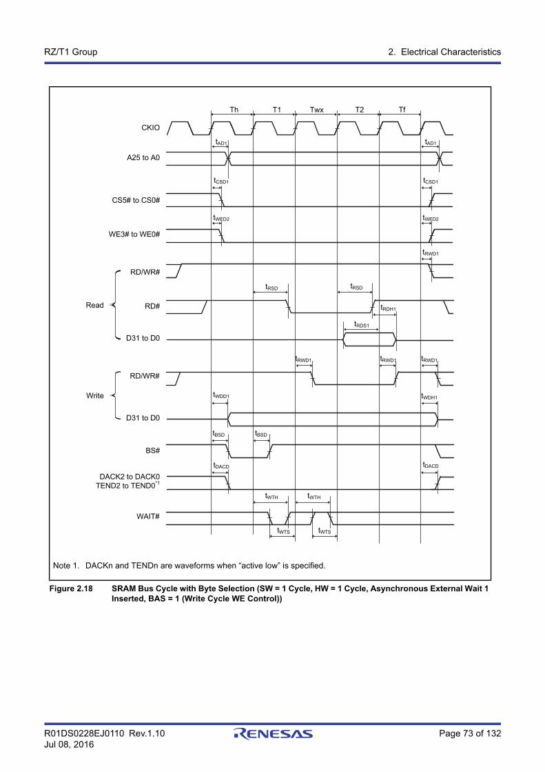
R01DS0228EJ0110 Rev.1.10 Page 73 of 132Jul 08, 2016
RZ/T1 Group 2. Electrical Characteristics
Note 1. DACKn and TENDn are waveforms when “active low” is specified.
Figure 2.18 SRAM Bus Cycle with Byte Selection (SW = 1 Cycle, HW = 1 Cycle, Asynchronous External Wait 1 Inserted, BAS = 1 (Write Cycle WE Control))
Th T2
tAD1 tAD1
tCSD1 tCSD1
tRWD1
tRDS1
tWED2 tWED2
tWDH1tWDD1
tBSD
tDACD tDACD
CKIO
A25 to A0
CS5# to CS0#
RD/WR#
RD#
D31 to D0
WE3# to WE0#
D31 to D0
BS#
DACK2 to DACK0TEND2 to TEND0*1
Read
Write
WAIT#
T1 Twx
tRSD
tWTH tWTH
tWTS tWTS
RD/WR#
Tf
tRSD
tRDH1
tRWD1 tRWD1
tBSD
tRWD1
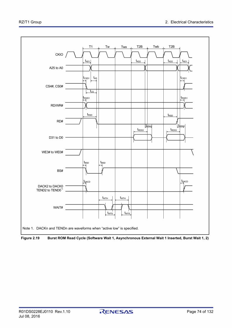
R01DS0228EJ0110 Rev.1.10 Page 74 of 132Jul 08, 2016
RZ/T1 Group 2. Electrical Characteristics
Note 1. DACKn and TENDn are waveforms when “active low” is specified.
Figure 2.19 Burst ROM Read Cycle (Software Wait 1, Asynchronous External Wait 1 Inserted, Burst Wait 1, 2)
T2B
tAD1 tAD1
tCSD1 tCSD1
tRWD1
tRDS3
tBSD
tDACD tDACD
CKIO
A25 to A0
CS4#, CS0#
RD/WR#
RD#
D31 to D0
WE3# to WE0#
BS#
DACK2 to DACK0TEND2 to TEND0*1
WAIT#
T1 Tw
tRSD
tWTH tWTH
tWTS tWTS
Twb
tRSD
tBSD
Twx T2B
tAD2 tAD2
tAS
tCS
tRWD1
tRDS3
tRDH3 tRDH3
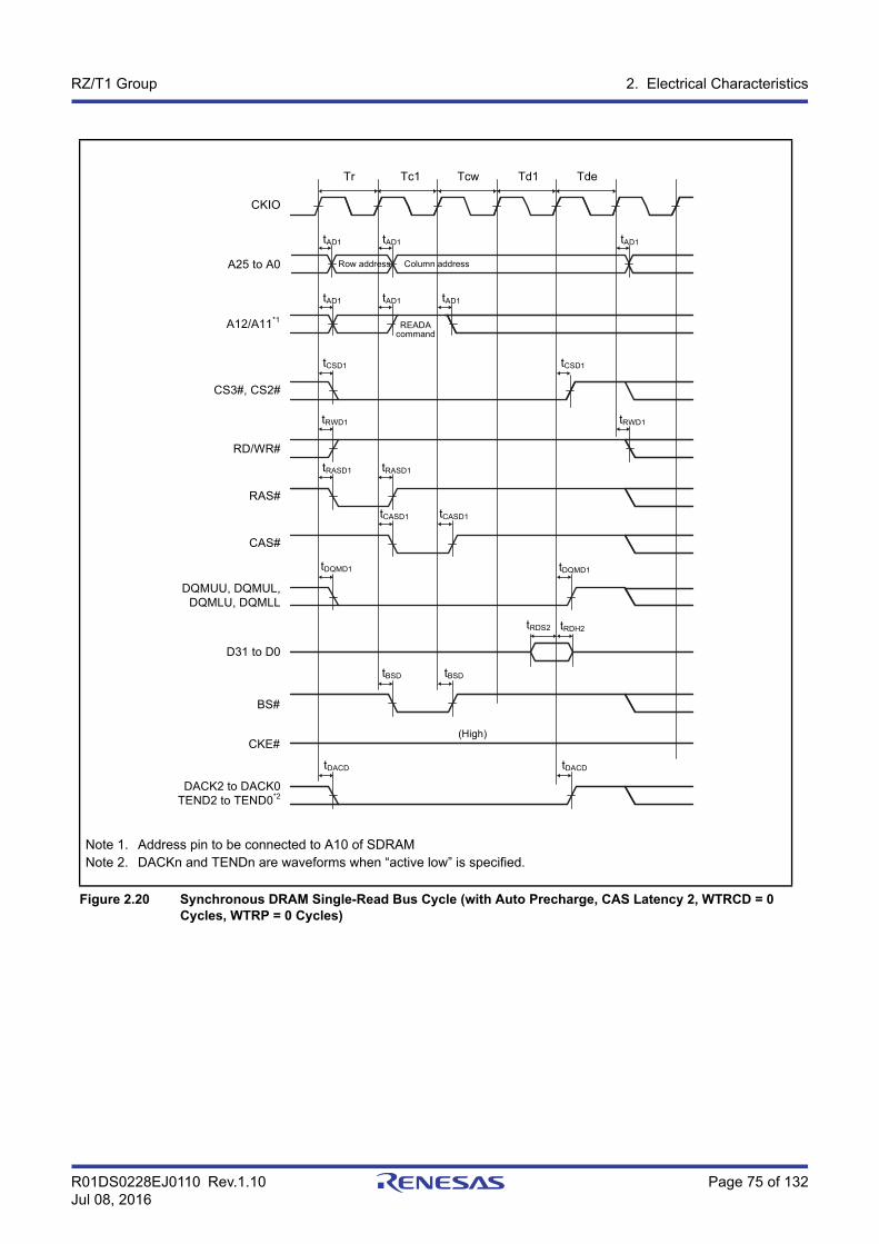
R01DS0228EJ0110 Rev.1.10 Page 75 of 132Jul 08, 2016
RZ/T1 Group 2. Electrical Characteristics
Note 1. Address pin to be connected to A10 of SDRAMNote 2. DACKn and TENDn are waveforms when “active low” is specified.
Figure 2.20 Synchronous DRAM Single-Read Bus Cycle (with Auto Precharge, CAS Latency 2, WTRCD = 0 Cycles, WTRP = 0 Cycles)
Td1
tAD1 tAD1
tCSD1
tRWD1
tBSD
tDACD
CKIO
A25 to A0
CS3#, CS2#
RD/WR#
RAS#
D31 to D0
CAS#
DQMUU, DQMUL, DQMLU, DQMLL
DACK2 to DACK0TEND2 to TEND0*2
BS#
Tr Tc1 Tde
tBSD
Tcw
A12/A11*1
CKE#
tAD1
tAD1 tAD1 tAD1
tCSD1
tRWD1
tRASD1 tRASD1
tCASD1 tCASD1
tDACD
(High)
tRDS2 tRDH2
tDQMD1 tDQMD1
Row address Column address
READAcommand
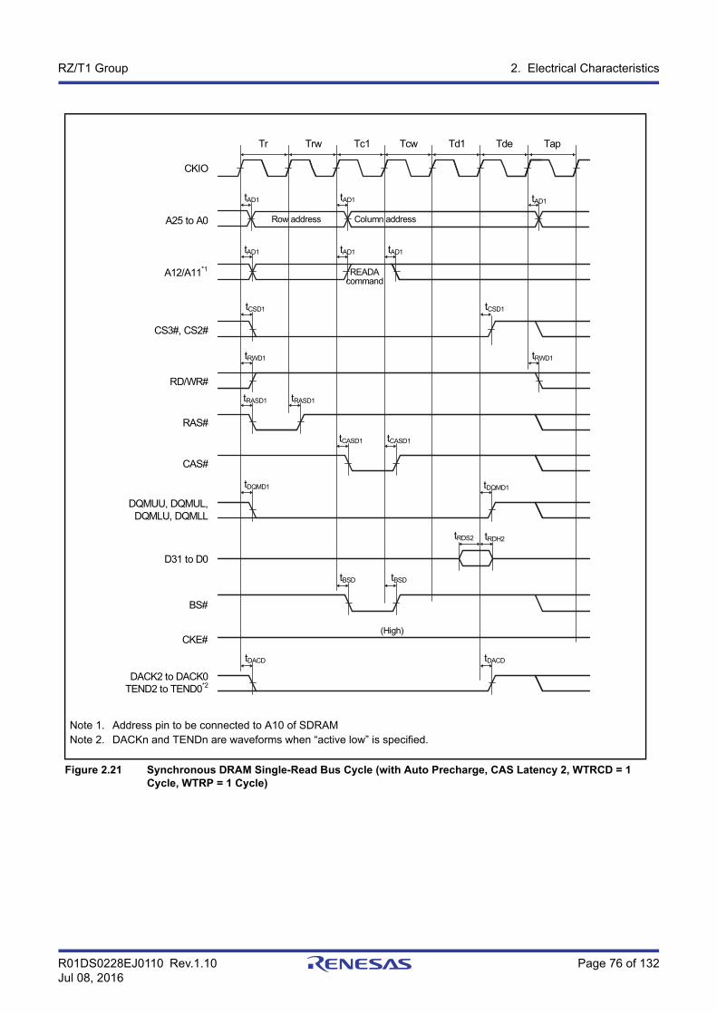
R01DS0228EJ0110 Rev.1.10 Page 76 of 132Jul 08, 2016
RZ/T1 Group 2. Electrical Characteristics
Note 1. Address pin to be connected to A10 of SDRAMNote 2. DACKn and TENDn are waveforms when “active low” is specified.
Figure 2.21 Synchronous DRAM Single-Read Bus Cycle (with Auto Precharge, CAS Latency 2, WTRCD = 1 Cycle, WTRP = 1 Cycle)
Td1
tAD1 tAD1
tCSD1
tRWD1
tBSD
tDACD
CKIO
A25 to A0
CS3#, CS2#
RD/WR#
RAS#
D31 to D0
CAS#
DQMUU, DQMUL, DQMLU, DQMLL
DACK2 to DACK0TEND2 to TEND0*2
BS#
Tr Tc1 Tde
tBSD
Tcw
A12/A11*1
CKE#
tAD1
tAD1 tAD1 tAD1
tCSD1
tRWD1
tRASD1 tRASD1
tCASD1 tCASD1
tDACD
(High)
tRDS2 tRDH2
tDQMD1 tDQMD1
Trw Tap
Row address Column address
READAcommand
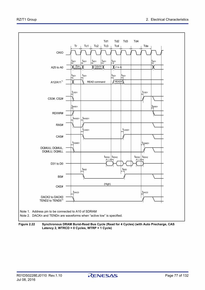
R01DS0228EJ0110 Rev.1.10 Page 77 of 132Jul 08, 2016
RZ/T1 Group 2. Electrical Characteristics
Note 1. Address pin to be connected to A10 of SDRAMNote 2. DACKn and TENDn are waveforms when “active low” is specified.
Figure 2.22 Synchronous DRAM Burst-Read Bus Cycle (Read for 4 Cycles) (with Auto Precharge, CAS Latency 2, WTRCD = 0 Cycles, WTRP = 1 Cycle)
Tc4
tAD1 tAD1
tCSD1
tRWD1
tBSD
tDACD
CKIO
A25 to A0
CS3#, CS2#
RD/WR#
RAS#
D31 to D0
CAS#
DQMUU, DQMUL, DQMLU, DQMLL
DACK2 to DACK0TEND2 to TEND0*2
BS#
Tr Tc1 Tde
tBSD
Tc3
A12/A11*1
CKE#
tAD1
tAD1 tAD1 tAD1
tCSD1
tRWD1
tRASD1 tRASD1
tCASD1 tCASD1
tDACD
(High)
tRDS2 tRDH2
tDQMD1 tDQMD1
Rowaddress
Columnaddress
READAcommand
Tc2
Td4Td1 Td3Td2
tAD1 tAD1 tAD1
tAD1
(1 to 4)
tRDS2 tRDH2
READ command
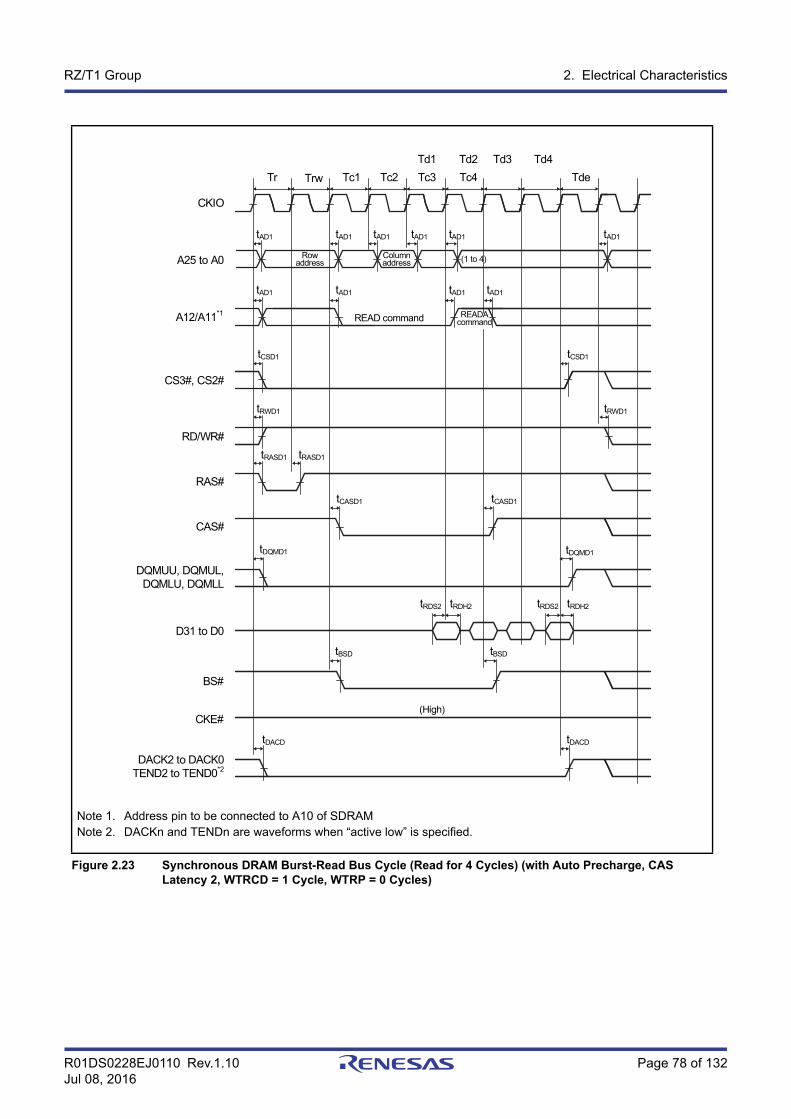
R01DS0228EJ0110 Rev.1.10 Page 78 of 132Jul 08, 2016
RZ/T1 Group 2. Electrical Characteristics
Note 1. Address pin to be connected to A10 of SDRAMNote 2. DACKn and TENDn are waveforms when “active low” is specified.
Figure 2.23 Synchronous DRAM Burst-Read Bus Cycle (Read for 4 Cycles) (with Auto Precharge, CAS Latency 2, WTRCD = 1 Cycle, WTRP = 0 Cycles)
Tc4
tAD1 tAD1
tCSD1
tRWD1
tBSD
tDACD
CKIO
A25 to A0
CS3#, CS2#
RD/WR#
RAS#
D31 to D0
CAS#
DQMUU, DQMUL, DQMLU, DQMLL
DACK2 to DACK0TEND2 to TEND0*2
BS#
Tr Tc1 Tde
tBSD
Tc3
A12/A11*1
CKE#
tAD1
tAD1 tAD1 tAD1
tCSD1
tRWD1
tRASD1 tRASD1
tCASD1 tCASD1
tDACD
(High)
tRDS2 tRDH2
tDQMD1 tDQMD1
Rowaddress
Columnaddress
Tc2
Td4Td1 Td3Td2
tAD1 tAD1 tAD1
tAD1
(1 to 4)
tRDS2 tRDH2
Trw
READAcommandREAD command
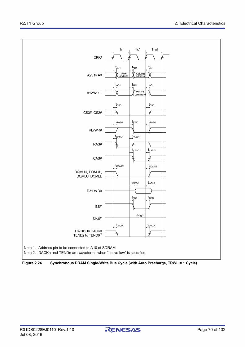
R01DS0228EJ0110 Rev.1.10 Page 79 of 132Jul 08, 2016
RZ/T1 Group 2. Electrical Characteristics
Note 1. Address pin to be connected to A10 of SDRAMNote 2. DACKn and TENDn are waveforms when “active low” is specified.
Figure 2.24 Synchronous DRAM Single-Write Bus Cycle (with Auto Precharge, TRWL = 1 Cycle)
tAD1 tAD1
tCSD1
tRWD1
tBSD
tDACD
CKIO
A25 to A0
CS3#, CS2#
RD/WR#
RAS#
D31 to D0
CAS#
DQMUU, DQMUL, DQMLU, DQMLL
DACK2 to DACK0TEND2 to TEND0*2
BS#
Tr Tc1
tBSD
A12/A11*1
CKE#
tAD1
tAD1 tAD1 tAD1
tCSD1
tRWD1
tRASD1 tRASD1
tCASD1 tCASD1
tDACD
(High)
tWDD2 tWDH2
tDQMD1 tDQMD1
Rowaddress
Columnaddress
WRITAcommand
Trwl
tRWD1
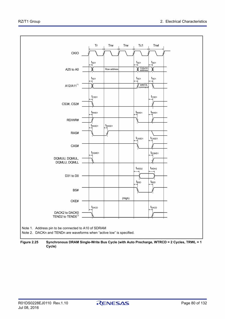
R01DS0228EJ0110 Rev.1.10 Page 80 of 132Jul 08, 2016
RZ/T1 Group 2. Electrical Characteristics
Note 1. Address pin to be connected to A10 of SDRAMNote 2. DACKn and TENDn are waveforms when “active low” is specified.
Figure 2.25 Synchronous DRAM Single-Write Bus Cycle (with Auto Precharge, WTRCD = 2 Cycles, TRWL = 1 Cycle)
tAD1 tAD1
tCSD1
tRWD1
tBSD
tDACD
CKIO
A25 to A0
CS3#, CS2#
RD/WR#
RAS#
D31 to D0
CAS#
DQMUU, DQMUL, DQMLU, DQMLL
DACK2 to DACK0TEND2 to TEND0*2
BS#
Tr Tc1
tBSD
A12/A11*1
CKE#
tAD1
tAD1 tAD1 tAD1
tCSD1
tRWD1
tRASD1 tRASD1
tCASD1 tCASD1
tDACD
(High)
tWDD2 tWDH2
tDQMD1 tDQMD1
Row address Columnaddress
WRITAcommand
Trwl
tRWD1
Trw Trw
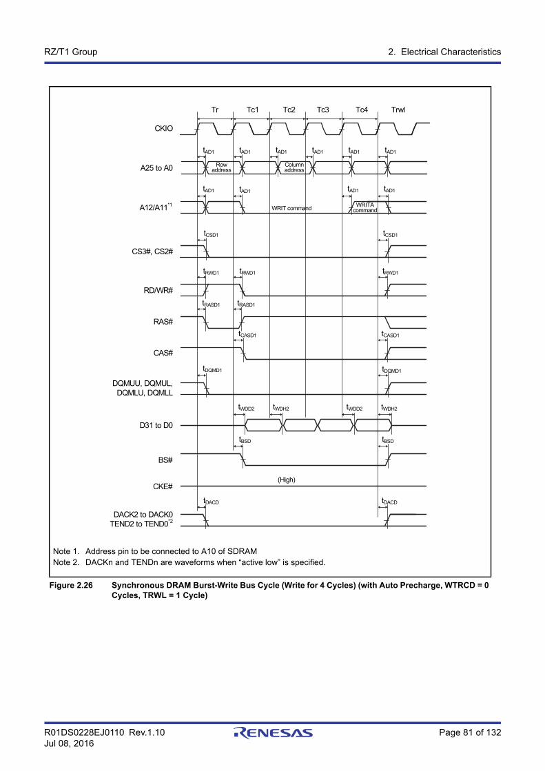
R01DS0228EJ0110 Rev.1.10 Page 81 of 132Jul 08, 2016
RZ/T1 Group 2. Electrical Characteristics
Note 1. Address pin to be connected to A10 of SDRAMNote 2. DACKn and TENDn are waveforms when “active low” is specified.
Figure 2.26 Synchronous DRAM Burst-Write Bus Cycle (Write for 4 Cycles) (with Auto Precharge, WTRCD = 0 Cycles, TRWL = 1 Cycle)
tAD1 tAD1
tCSD1
tRWD1
tBSD
tDACD
CKIO
A25 to A0
CS3#, CS2#
RD/WR#
RAS#
D31 to D0
CAS#
DQMUU, DQMUL, DQMLU, DQMLL
DACK2 to DACK0TEND2 to TEND0*2
BS#
Tr Tc3
tBSD
A12/A11*1
CKE#
tAD1
tAD1 tAD1 tAD1
tCSD1
tRWD1
tRASD1 tRASD1
tCASD1 tCASD1
tDACD
(High)
tWDD2 tWDH2
tDQMD1 tDQMD1
Rowaddress
Columnaddress
WRITAcommand
Trwl
tRWD1
Tc1 Tc2 Tc4
tAD1 tAD1 tAD1
tAD1
WRIT command
tWDD2 tWDH2

R01DS0228EJ0110 Rev.1.10 Page 82 of 132Jul 08, 2016
RZ/T1 Group 2. Electrical Characteristics
Note 1. Address pin to be connected to A10 of SDRAMNote 2. DACKn and TENDn are waveforms when “active low” is specified.
Figure 2.27 Synchronous DRAM Burst-Write Bus Cycle (Write for 4 Cycles) (with Auto Precharge, WTRCD = 1 Cycle, TRWL = 1 Cycle)
tAD1 tAD1
tCSD1
tRWD1
tBSD
tDACD
CKIO
A25 to A0
CS3#, CS2#
RD/WR#
RAS#
D31 to D0
CAS#
DQMUU, DQMUL, DQMLU, DQMLL
DACK2 to DACK0TEND2 to TEND0*2
BS#
Tr Tc3
tBSD
A12/A11*1
CKE#
tAD1
tAD1 tAD1 tAD1
tCSD1
tRWD1
tRASD1 tRASD1
tCASD1 tCASD1
tDACD
(High)
tWDD2 tWDH2
tDQMD1 tDQMD1
Rowaddress
Columnaddress
WRITAcommand
Trwl
tRWD1
Tc1 Tc2 Tc4
tAD1 tAD1 tAD1
tAD1
WRIT command
tWDD2 tWDH2
Trw
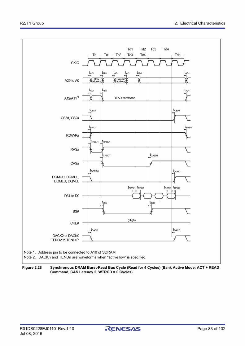
R01DS0228EJ0110 Rev.1.10 Page 83 of 132Jul 08, 2016
RZ/T1 Group 2. Electrical Characteristics
Note 1. Address pin to be connected to A10 of SDRAMNote 2. DACKn and TENDn are waveforms when “active low” is specified.
Figure 2.28 Synchronous DRAM Burst-Read Bus Cycle (Read for 4 Cycles) (Bank Active Mode: ACT + READ Command, CAS Latency 2, WTRCD = 0 Cycles)
Tc4
tAD1 tAD1
tCSD1
tRWD1
tBSD
tDACD
CKIO
A25 to A0
CS3#, CS2#
RD/WR#
RAS#
D31 to D0
CAS#
DQMUU, DQMUL, DQMLU, DQMLL
DACK2 to DACK0TEND2 to TEND0*2
BS#
Tr Tc1 Tde
tBSD
Tc3
A12/A11*1
CKE#
tAD1
tAD1 tAD1
tCSD1
tRWD1
tRASD1 tRASD1
tCASD1 tCASD1
tDACD
(High)
tRDS2 tRDH2
tDQMD1 tDQMD1
Rowaddress
Columnaddress
Tc2
Td4Td1 Td3Td2
tAD1 tAD1 tAD1
tAD1
tRDS2 tRDH2
READ command
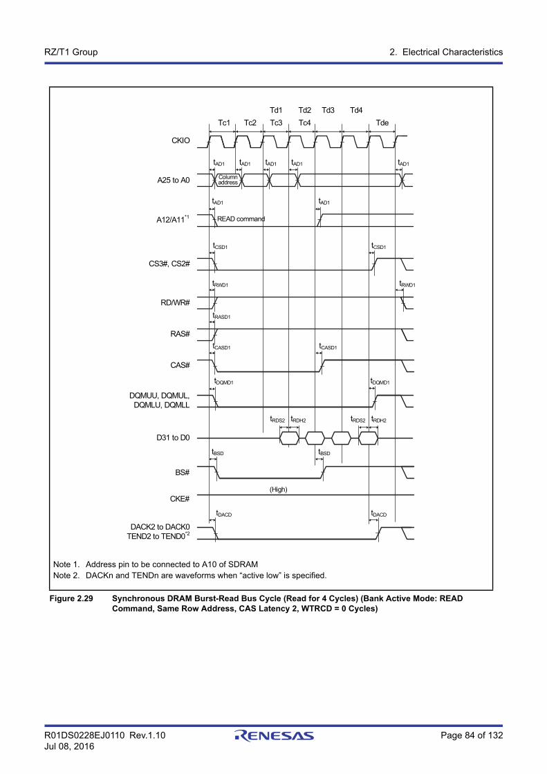
R01DS0228EJ0110 Rev.1.10 Page 84 of 132Jul 08, 2016
RZ/T1 Group 2. Electrical Characteristics
Note 1. Address pin to be connected to A10 of SDRAMNote 2. DACKn and TENDn are waveforms when “active low” is specified.
Figure 2.29 Synchronous DRAM Burst-Read Bus Cycle (Read for 4 Cycles) (Bank Active Mode: READ Command, Same Row Address, CAS Latency 2, WTRCD = 0 Cycles)
Tc4
tAD1
tCSD1
tRWD1
tBSD
tDACD
CKIO
A25 to A0
CS3#, CS2#
RD/WR#
RAS#
D31 to D0
CAS#
DQMUU, DQMUL, DQMLU, DQMLL
DACK2 to DACK0TEND2 to TEND0*2
BS#
Tc1 Tde
tBSD
Tc3
A12/A11*1
CKE#
tAD1
tAD1 tAD1
tCSD1
tRWD1
tRASD1
tCASD1 tCASD1
tDACD
(High)
tRDS2 tRDH2
tDQMD1 tDQMD1
Columnaddress
Tc2
Td4Td1 Td3Td2
tAD1 tAD1 tAD1
tRDS2 tRDH2
READ command

R01DS0228EJ0110 Rev.1.10 Page 85 of 132Jul 08, 2016
RZ/T1 Group 2. Electrical Characteristics
Note 1. Address pin to be connected to A10 of SDRAMNote 2. DACKn and TENDn are waveforms when “active low” is specified.
Figure 2.30 Synchronous DRAM Burst-Read Bus Cycle (Read for 4 Cycles) (Bank Active Mode: PRE + ACT + READ Command, Different Row Address, CAS Latency 2, WTRCD = 0 Cycles)
Tc4
tAD1 tAD1
tCSD1
tRWD1
tBSD
tDACD
CKIO
A25 to A0
CS3#, CS2#
RD/WR#
RAS#
D31 to D0
CAS#
DQMUU, DQMUL, DQMLU, DQMLL
DACK2 to DACK0TEND2 to TEND0*2
BS#
Tr Tc1 Tde
tBSD
Tc3
A12/A11*1
CKE#
tAD1
tAD1 tAD1
tCSD1
tRWD1
tRASD1 tRASD1
tCASD1 tCASD1
tDACD
(High)
tRDS2 tRDH2
tDQMD1 tDQMD1
Rowaddress
Columnaddress
Tc2
Td4Td1 Td3Td2
tAD1 tAD1 tAD1
tAD1
tRDS2 tRDH2
READ command
Tp Trw
tAD1
tRWD1
tRASD1 tRASD1
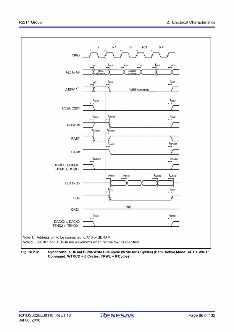
R01DS0228EJ0110 Rev.1.10 Page 86 of 132Jul 08, 2016
RZ/T1 Group 2. Electrical Characteristics
Note 1. Address pin to be connected to A10 of SDRAMNote 2. DACKn and TENDn are waveforms when “active low” is specified.
Figure 2.31 Synchronous DRAM Burst-Write Bus Cycle (Write for 4 Cycles) (Bank Active Mode: ACT + WRITE Command, WTRCD = 0 Cycles, TRWL = 0 Cycles)
tAD1 tAD1
tCSD1
tRWD1
tBSD
tDACD
CKIO
A25 to A0
CS3#, CS2#
RD/WR#
RAS#
D31 to D0
CAS#
DQMUU, DQMUL, DQMLU, DQMLL
DACK2 to DACK0TEND2 to TEND0*2
BS#
Tr Tc3
tBSD
A12/A11*1
CKE#
tAD1
tAD1 tAD1
tCSD1
tRWD1
tRASD1 tRASD1
tCASD1 tCASD1
tDACD
(High)
tWDD2 tWDH2
tDQMD1 tDQMD1
Rowaddress
Columnaddress
tRWD1
Tc1 Tc2 Tc4
tAD1 tAD1 tAD1
tAD1
WRIT command
tWDD2 tWDH2
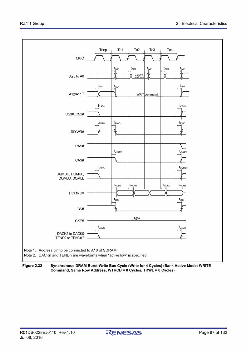
R01DS0228EJ0110 Rev.1.10 Page 87 of 132Jul 08, 2016
RZ/T1 Group 2. Electrical Characteristics
Note 1. Address pin to be connected to A10 of SDRAMNote 2. DACKn and TENDn are waveforms when “active low” is specified.
Figure 2.32 Synchronous DRAM Burst-Write Bus Cycle (Write for 4 Cycles) (Bank Active Mode: WRITE Command, Same Row Address, WTRCD = 0 Cycles, TRWL = 0 Cycles)
tAD1
tCSD1
tRWD1
tBSD
tDACD
CKIO
A25 to A0
CS3#, CS2#
RD/WR#
RAS#
D31 to D0
CAS#
DQMUU, DQMUL, DQMLU, DQMLL
DACK2 to DACK0TEND2 to TEND0*2
BS#
Tnop Tc3
tBSD
A12/A11*1
CKE#
tAD1
tAD1 tAD1
tCSD1
tRWD1
tCASD1 tCASD1
tDACD
(High)
tWDD2 tWDH2
tDQMD1 tDQMD1
Columnaddress
tRWD1
Tc1 Tc2 Tc4
tAD1 tAD1 tAD1
tAD1
WRIT command
tWDD2 tWDH2
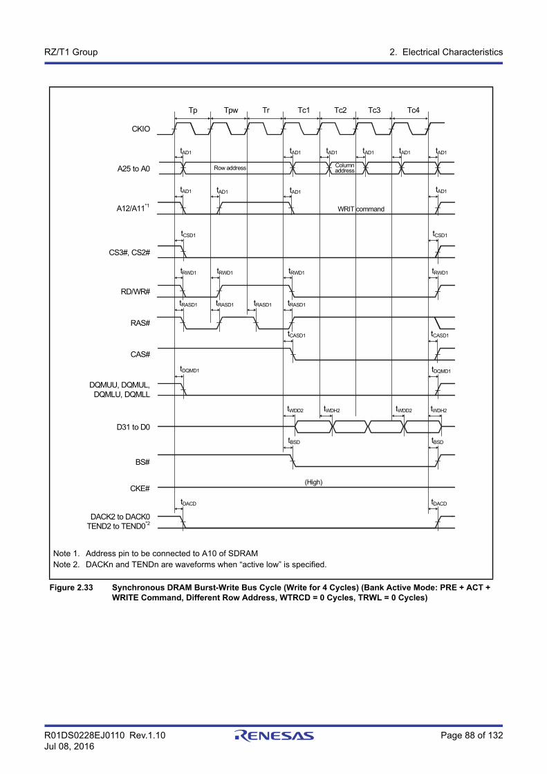
R01DS0228EJ0110 Rev.1.10 Page 88 of 132Jul 08, 2016
RZ/T1 Group 2. Electrical Characteristics
Note 1. Address pin to be connected to A10 of SDRAMNote 2. DACKn and TENDn are waveforms when “active low” is specified.
Figure 2.33 Synchronous DRAM Burst-Write Bus Cycle (Write for 4 Cycles) (Bank Active Mode: PRE + ACT + WRITE Command, Different Row Address, WTRCD = 0 Cycles, TRWL = 0 Cycles)
tAD1 tAD1
tCSD1
tRWD1
tBSD
tDACD
CKIO
A25 to A0
CS3#, CS2#
RD/WR#
RAS#
D31 to D0
CAS#
DQMUU, DQMUL, DQMLU, DQMLL
DACK2 to DACK0TEND2 to TEND0*2
BS#
Tr Tc3
tBSD
A12/A11*1
CKE#
tAD1
tAD1 tAD1
tCSD1
tRWD1
tRASD1 tRASD1
tCASD1 tCASD1
tDACD
(High)
tWDD2 tWDH2
tDQMD1 tDQMD1
Row address Columnaddress
tRWD1
Tc1 Tc2 Tc4
tAD1 tAD1 tAD1
tAD1
WRIT command
tWDD2 tWDH2
Tp Tpw
tAD1
tRWD1
tRASD1 tRASD1

R01DS0228EJ0110 Rev.1.10 Page 89 of 132Jul 08, 2016
RZ/T1 Group 2. Electrical Characteristics
Note 1. Address pin to be connected to A10 of SDRAMNote 2. DACKn and TENDn are waveforms when “active low” is specified.
Figure 2.34 Synchronous DRAM Auto-Refresh Timing (WTRP = 1 Cycle, WTRC = 3 Cycles)
tAD1
tCSD1
tRWD1
CKIO
A25 toA0
CS3#, CS2#
RD/WR#
RAS#
D31 to D0
CAS#
DQMUU, DQMUL, DQMLU, DQMLL
DACK2 to DACK0TEND2 to TEND0*2
BS#
Trr Trc
A12/A11*1
CKE#
tAD1
tRWD1
tRASD1 tRASD1
tCASD1
(High)
Trc Trc
tAD1
Tp Tpw
tAD1
tRWD1
tRASD1 tRASD1
tCSD1 tCSD1 tCSD1
tCASD1
(Hi-Z)
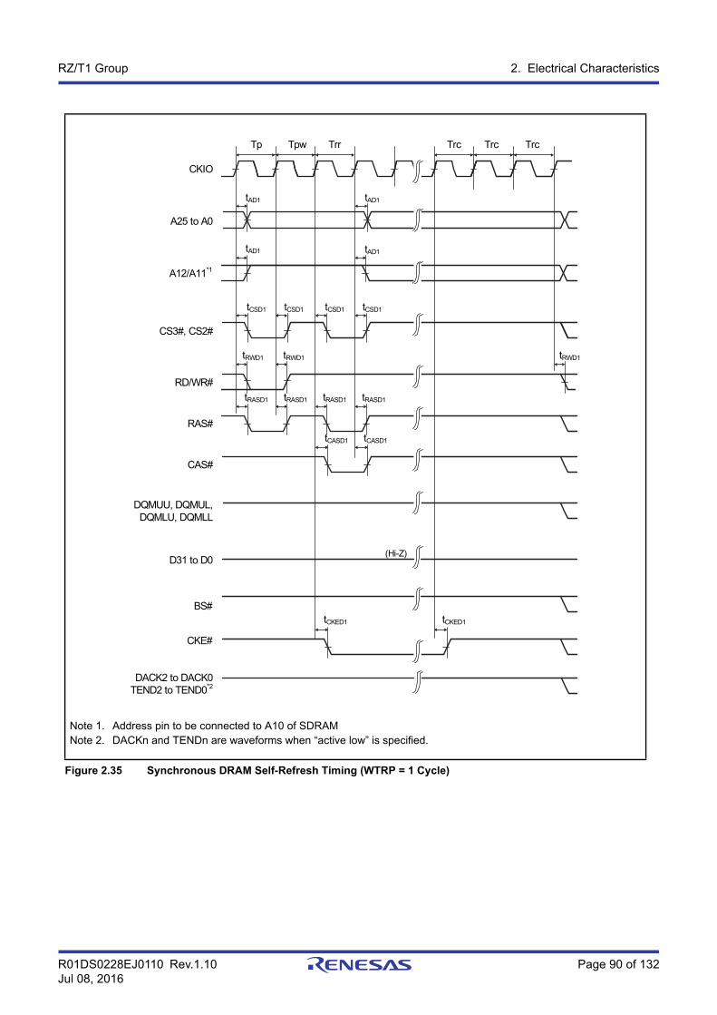
R01DS0228EJ0110 Rev.1.10 Page 90 of 132Jul 08, 2016
RZ/T1 Group 2. Electrical Characteristics
Note 1. Address pin to be connected to A10 of SDRAMNote 2. DACKn and TENDn are waveforms when “active low” is specified.
Figure 2.35 Synchronous DRAM Self-Refresh Timing (WTRP = 1 Cycle)
tAD1
tCSD1
tRWD1
CKIO
A25 to A0
CS3#, CS2#
RD/WR#
RAS#
D31 to D0
CAS#
DQMUU, DQMUL, DQMLU, DQMLL
DACK2 to DACK0TEND2 to TEND0*2
BS#
Trr Trc
A12/A11*1
CKE#
tAD1
tRWD1
tRASD1 tRASD1
tCASD1
Trc Trc
tAD1
Tp Tpw
tAD1
tRWD1
tRASD1 tRASD1
tCSD1 tCSD1 tCSD1
tCASD1
(Hi-Z)
tCKED1 tCKED1
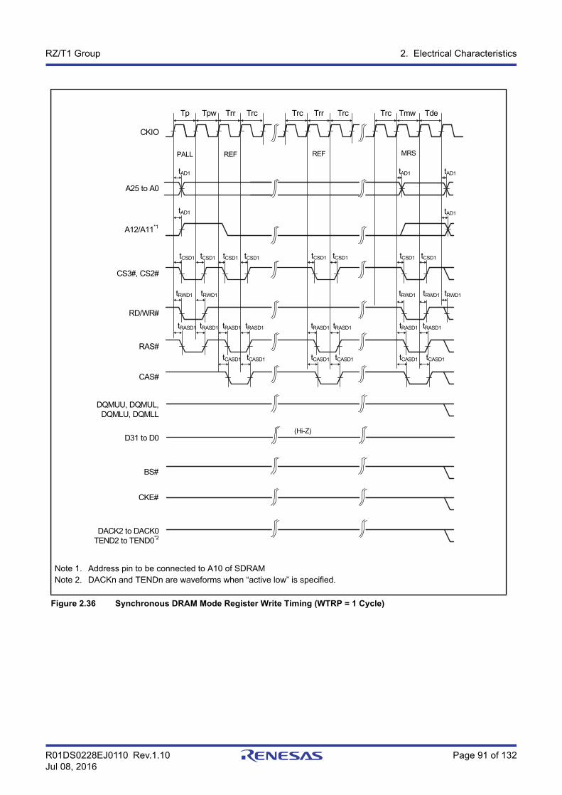
R01DS0228EJ0110 Rev.1.10 Page 91 of 132Jul 08, 2016
RZ/T1 Group 2. Electrical Characteristics
Note 1. Address pin to be connected to A10 of SDRAMNote 2. DACKn and TENDn are waveforms when “active low” is specified.
Figure 2.36 Synchronous DRAM Mode Register Write Timing (WTRP = 1 Cycle)
tAD1
tCSD1
tRWD1
CKIO
A25 to A0
CS3#, CS2#
RD/WR#
RAS#
D31 to D0
CAS#
DQMUU, DQMUL, DQMLU, DQMLL
DACK2 to DACK0TEND2 to TEND0*2
BS#
Trr Trc
A12/A11*1
CKE#
tAD1
tRASD1 tRASD1
tCASD1
Trc Trc
tAD1
Tp Tpw
tAD1
tRWD1
tRASD1 tRASD1
tCSD1 tCSD1 tCSD1
tCASD1
(Hi-Z)
Trr Trc Tmw Tde
tAD1
tCSD1 tCSD1 tCSD1 tCSD1
tRWD1 tRWD1 tRWD1
tRASD1 tRASD1tRASD1 tRASD1
tCASD1 tCASD1 tCASD1 tCASD1
PALL REF REF MRS
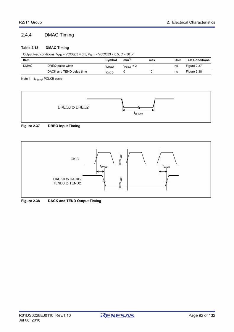
R01DS0228EJ0110 Rev.1.10 Page 92 of 132Jul 08, 2016
RZ/T1 Group 2. Electrical Characteristics
2.4.4 DMAC Timing
Note 1. tPBcyc: PCLKB cycle
Table 2.18 DMAC Timing
Output load conditions: VOH = VCCQ33 × 0.5, VOL1 = VCCQ33 × 0.5, C = 30 pF
Item Symbol min*1 max Unit Test Conditions
DMAC DREQ pulse width tDRQW tPBcyc × 2 ― ns Figure 2.37
DACK and TEND delay time tDACD 0 10 ns Figure 2.38
Figure 2.37 DREQ Input Timing
Figure 2.38 DACK and TEND Output Timing
DREQ0 to DREQ2
tDRQW
DACK0 to DACK2TEND0 to TEND2
tDACD
CKIO
tDACD
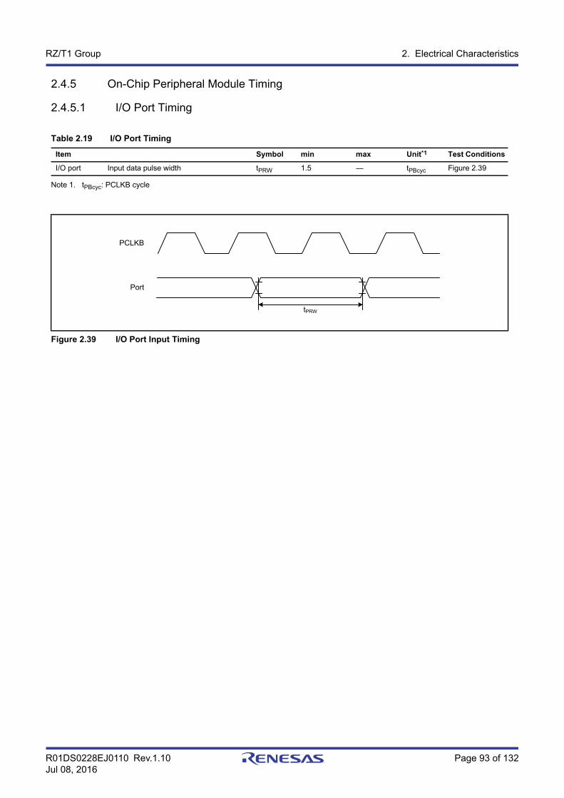
R01DS0228EJ0110 Rev.1.10 Page 93 of 132Jul 08, 2016
RZ/T1 Group 2. Electrical Characteristics
2.4.5 On-Chip Peripheral Module Timing
2.4.5.1 I/O Port Timing
Note 1. tPBcyc: PCLKB cycle
Table 2.19 I/O Port Timing
Item Symbol min max Unit*1 Test Conditions
I/O port Input data pulse width tPRW 1.5 ― tPBcyc Figure 2.39
Figure 2.39 I/O Port Input Timing
Port
PCLKB
tPRW
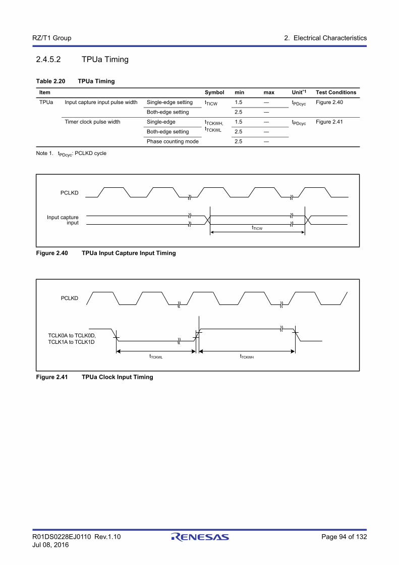
R01DS0228EJ0110 Rev.1.10 Page 94 of 132Jul 08, 2016
RZ/T1 Group 2. Electrical Characteristics
2.4.5.2 TPUa Timing
Note 1. tPDcyc: PCLKD cycle
Table 2.20 TPUa Timing
Item Symbol min max Unit*1 Test Conditions
TPUa Input capture input pulse width Single-edge setting tTICW 1.5 ― tPDcyc Figure 2.40
Both-edge setting 2.5 ―
Timer clock pulse width Single-edge tTCKWH, tTCKWL
1.5 ― tPDcyc Figure 2.41
Both-edge setting 2.5 ―
Phase counting mode 2.5 ―
Figure 2.40 TPUa Input Capture Input Timing
Figure 2.41 TPUa Clock Input Timing
Input capture input
PCLKD
tTICW
TCLK0A to TCLK0D, TCLK1A to TCLK1D
PCLKD
tTCKWL tTCKWH
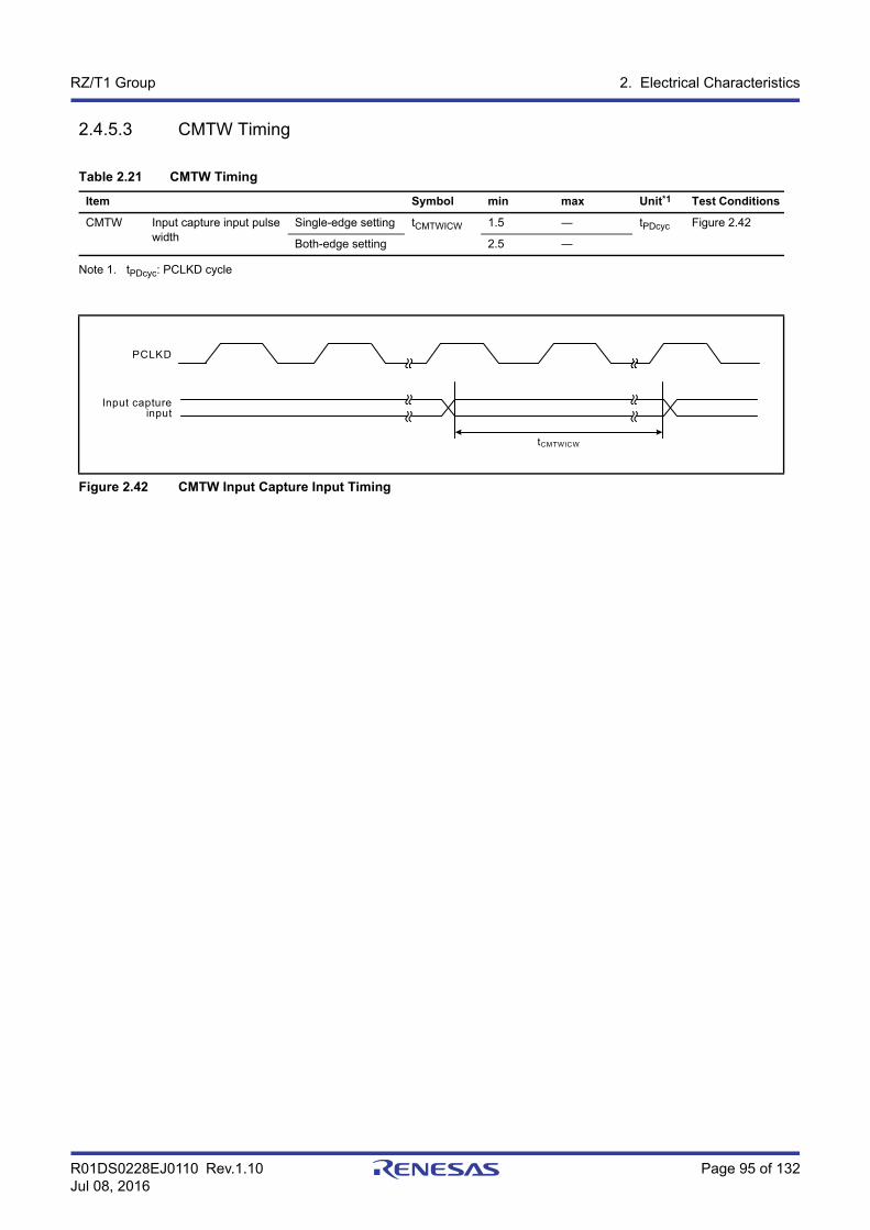
R01DS0228EJ0110 Rev.1.10 Page 95 of 132Jul 08, 2016
RZ/T1 Group 2. Electrical Characteristics
2.4.5.3 CMTW Timing
Note 1. tPDcyc: PCLKD cycle
Table 2.21 CMTW Timing
Item Symbol min max Unit*1 Test Conditions
CMTW Input capture input pulse width
Single-edge setting tCMTWICW 1.5 ― tPDcyc Figure 2.42
Both-edge setting 2.5 ―
Figure 2.42 CMTW Input Capture Input Timing
Input capture input
PCLKD
tCMTWICW
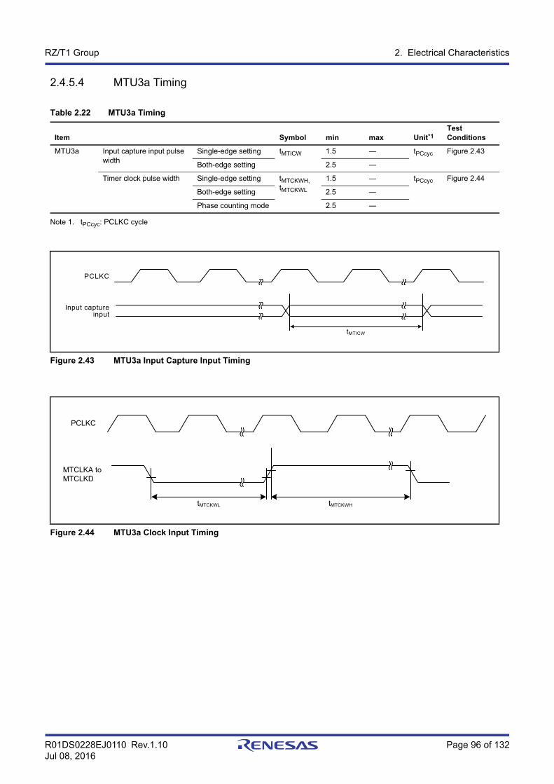
R01DS0228EJ0110 Rev.1.10 Page 96 of 132Jul 08, 2016
RZ/T1 Group 2. Electrical Characteristics
2.4.5.4 MTU3a Timing
Note 1. tPCcyc: PCLKC cycle
Table 2.22 MTU3a Timing
Item Symbol min max Unit*1Test Conditions
MTU3a Input capture input pulse width
Single-edge setting tMTICW 1.5 ― tPCcyc Figure 2.43
Both-edge setting 2.5 ―
Timer clock pulse width Single-edge setting tMTCKWH, tMTCKWL
1.5 ― tPCcyc Figure 2.44
Both-edge setting 2.5 ―
Phase counting mode 2.5 ―
Figure 2.43 MTU3a Input Capture Input Timing
Figure 2.44 MTU3a Clock Input Timing
Input capture input
PCLKC
tMTICW
MTCLKA to MTCLKD
PCLKC
tMTCKWL tMTCKWH

R01DS0228EJ0110 Rev.1.10 Page 97 of 132Jul 08, 2016
RZ/T1 Group 2. Electrical Characteristics
2.4.5.5 POE3 Timing
Note 1. tPDcyc: PCLKD cycle
Table 2.23 POE3 Timing
Item Symbol min max Unit*1 Test Conditions
POE3 POEn# input pulse width tPOEW 1.5 ― tPDcyc Figure 2.45
Figure 2.45 POEn# Input Pulse Timing
POEn# input
PCLKD
tPOEW
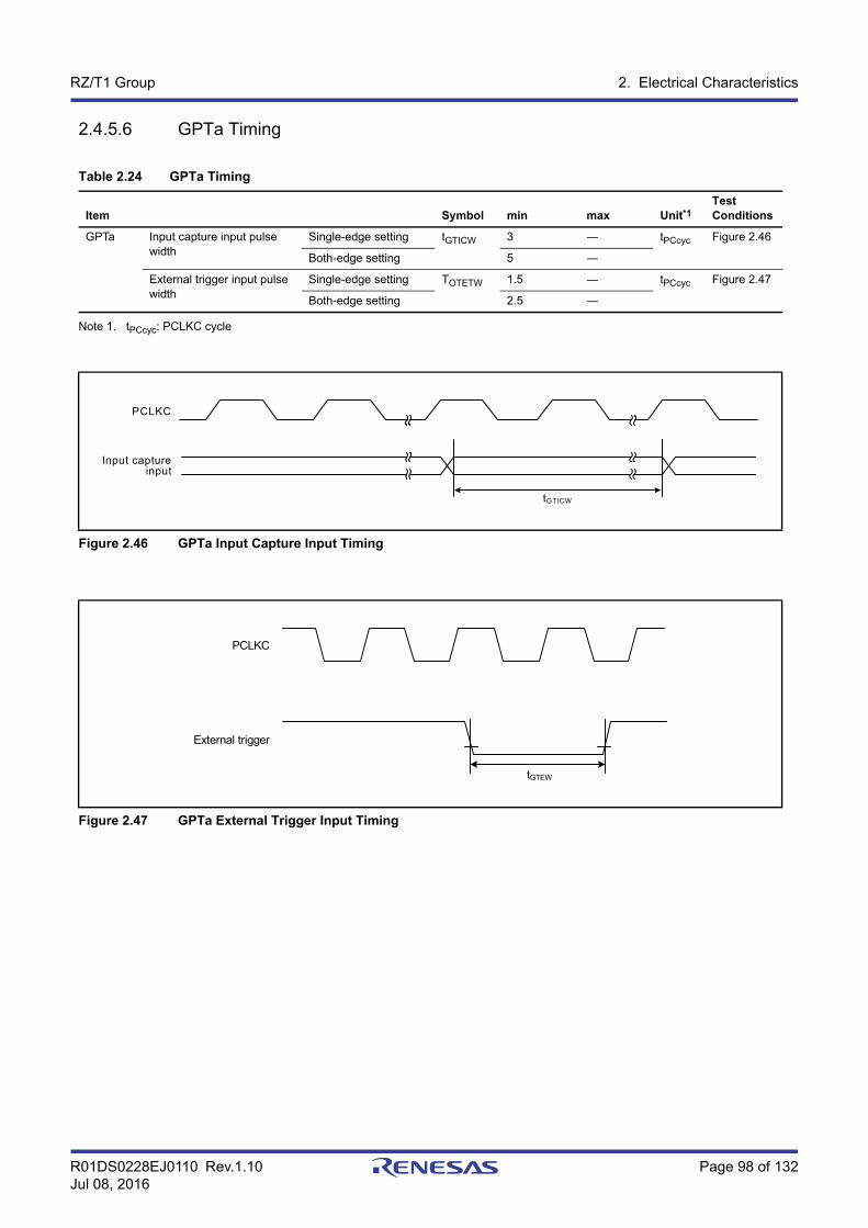
R01DS0228EJ0110 Rev.1.10 Page 98 of 132Jul 08, 2016
RZ/T1 Group 2. Electrical Characteristics
2.4.5.6 GPTa Timing
Note 1. tPCcyc: PCLKC cycle
Table 2.24 GPTa Timing
Item Symbol min max Unit*1Test Conditions
GPTa Input capture input pulse width
Single-edge setting tGTICW 3 ― tPCcyc Figure 2.46
Both-edge setting 5 ―
External trigger input pulse width
Single-edge setting TOTETW 1.5 ― tPCcyc Figure 2.47
Both-edge setting 2.5 ―
Figure 2.46 GPTa Input Capture Input Timing
Figure 2.47 GPTa External Trigger Input Timing
Input capture input
PCLKC
tGTICW
External trigger
PCLKC
tGTEW

R01DS0228EJ0110 Rev.1.10 Page 99 of 132Jul 08, 2016
RZ/T1 Group 2. Electrical Characteristics
2.4.5.7 A/D Converter Trigger Timing
Note 1. tPFcyc: PCLKF cycle, tPGcyc: PCLKG cycle
Table 2.25 A/D Converter Trigger Timing
Item Symbol min max Unit*1Test Conditions
A/D converter A/D converter trigger input pulse width
ADTRG0 tTRGW 1.5 ― tPFcyc Figure 2.48
ADTRG1 1.5 tPGcyc Figure 2.49
Figure 2.48 A/D Converter Trigger Input Timing (ADTRG0)
Figure 2.49 A/D Converter Trigger Input Timing (ADTRG1)
ADTRG0
PCLKF
tTRGW
ADTRG1
PCLKG
tTRGW
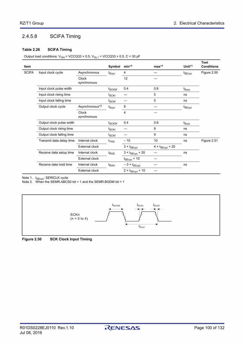
R01DS0228EJ0110 Rev.1.10 Page 100 of 132Jul 08, 2016
RZ/T1 Group 2. Electrical Characteristics
2.4.5.8 SCIFA Timing
Note 1. tSEcyc: SERICLK cycleNote 2. When the SEMR.ABCS0 bit = 1 and the SEMR.BGDM bit = 1
Table 2.26 SCIFA Timing
Output load conditions: VOH = VCCQ33 × 0.5, VOL1 = VCCQ33 × 0.5, C = 30 pF
Item Symbol min*1 max*1 Unit*1Test Conditions
SCIFA Input clock cycle Asynchronous tScyc 4 ― tSEcyc Figure 2.50
Clock synchronous
12 ―
Input clock pulse width tSCKW 0.4 0.6 tScyc
Input clock rising time tSCKr ― 5 ns
Input clock falling time tSCKf ― 5 ns
Output clock cycle Asynchronous*2 tScyc 8 ― tSEcyc
Clock synchronous
4 ―
Output clock pulse width tSCKW 0.4 0.6 tScyc
Output clock rising time tSCKr ― 9 ns
Output clock falling time tSCKf ― 9 ns
Transmit data delay time Internal clock tTXD – 10 10 ns Figure 2.51
External clock 3 × tSEcyc 4 × tSEcyc + 20
Receive data setup time Internal clock tRXS 3 × tSEcyc + 20 ― ns
External clock tSEcyc + 10 ―
Receive data hold time Internal clock tRXH – 3 × tSEcyc ― ns
External clock 2 × tSEcyc + 10 ―
Figure 2.50 SCK Clock Input Timing
tSCKW tSCKr tSCKf
tScyc
SCKn(n = 0 to 4)

R01DS0228EJ0110 Rev.1.10 Page 101 of 132Jul 08, 2016
RZ/T1 Group 2. Electrical Characteristics
Figure 2.51 SCIFA Input/Output Timing/Clock Synchronous Mode
tTXD
tRXS tRXH
TXDn
RXDn
SCKn
n = 0 to 4
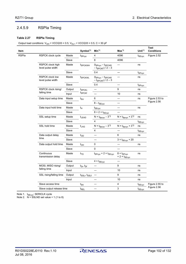
R01DS0228EJ0110 Rev.1.10 Page 102 of 132Jul 08, 2016
RZ/T1 Group 2. Electrical Characteristics
2.4.5.9 RSPIa Timing
Note 1. tSEcyc: SERICLK cycleNote 2. N = SSLND set value + 1 (1 to 8)
Table 2.27 RSPIa Timing
Output load conditions: VOH = VCCQ33 × 0.5, VOL1 = VCCQ33 × 0.5, C = 30 pF
Item Symbol*1 Min*1 Max*1 Unit*1Test Conditions
RSPIa RSPCK clock cycle Maste tSPcyc 4 4096 tSEcyc Figure 2.52
Slave 8 4096
RSPCK clock high level pulse width
Maste tSPCKWH (tSPcyc – tSPCKR– tSPCKF) / 2 – 3
― ns
Slave 0.4 ― tSPcyc
RSPCK clock low level pulse width
Maste tSPCKWL (tSPcyc – tSPCKR– tSPCKF) / 2 – 3
― ns
Slave 0.4 ― tSPcyc
RSPCK clock rising/falling time
Output tSPCKr, tSPCKf
― 9 ns
Input ― 10 ns
Data input setup time Maste tSU 6 ― ns Figure 2.53 to Figure 2.56
Slave 8 – tSEcyc ―
Data input hold time Maste tH tSEcyc ― ns
Slave 8 + 2 × tSEcyc ―
SSL setup time Maste tLEAD N × tSpcyc – 3*2 N × tSpcyc + 3*2 ns
Slave 4 ― tSEcyc
SSL hold time Maste tLAG N × tSpcyc – 3*2 N × tSpcyc + 3*2 ns
Slave 4 ― tSEcyc
Data output delay time
Maste tOD ― 6 ns
Slave ― 3 × tSEcyc + 20
Data output hold time Maste tOH 0 ― ns
Slave 0 ―
Continuous transmission delay
Maste tTD tSPcyc + 2 × tSEcyc 8 × tSPcyc+ 2 × tSEcyc
ns
Slave 4 × tSEcyc ―
MOSI, MISO rising/falling time
Output tDr, tDf ― 9 ns
Input ― 10 ns
SSL rising/falling time Output tSSLr, tSSLf ― 9 ns
Input ― 10 ns
Slave access time tSA ― 4 tSEcyc Figure 2.55 to Figure 2.56
Slave output release time tREL ― 3 tSEcyc
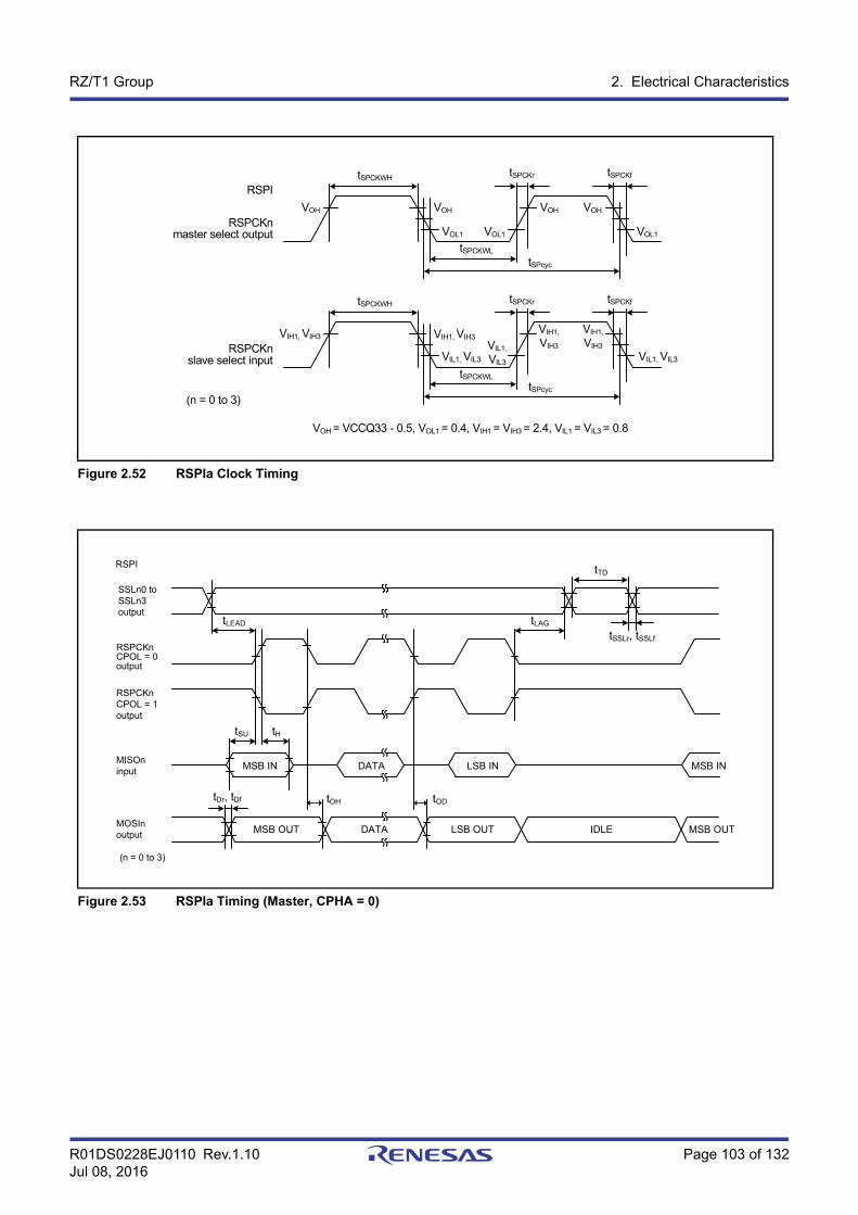
R01DS0228EJ0110 Rev.1.10 Page 103 of 132Jul 08, 2016
RZ/T1 Group 2. Electrical Characteristics
Figure 2.52 RSPIa Clock Timing
Figure 2.53 RSPIa Timing (Master, CPHA = 0)
RSPCKnmaster select output
RSPCKnslave select input
tSPCKWH
VOH VOH
VOL1 VOL1
VOH VOH
tSPCKWL
tSPCKr tSPCKf
VOL1
tSPcyc
tSPCKWH
VIH1, VIH3
tSPCKWL
tSPCKr tSPCKf
tSPcyc
VOH = VCCQ33 - 0.5, VOL1 = 0.4, VIH1 = VIH3 = 2.4, VIL1 = VIL3 = 0.8
RSPI
(n = 0 to 3)
VIH1, VIH3
VIL1, VIL3
VIL1,
VIL3
VIH1,
VIH3
VIH1,
VIH3
VIL1, VIL3
tDr, tDf
tSU tH
tLEAD
tTD
tLAG
tSSLr, tSSLf
tOH tOD
MSB IN DATA LSB IN MSB IN
MSB OUT DATA LSB OUT IDLE MSB OUT
SSLn0 to SSLn3output
RSPCKnCPOL = 0output
RSPCKnCPOL = 1output
MISOninput
MOSInoutput
RSPI
(n = 0 to 3)
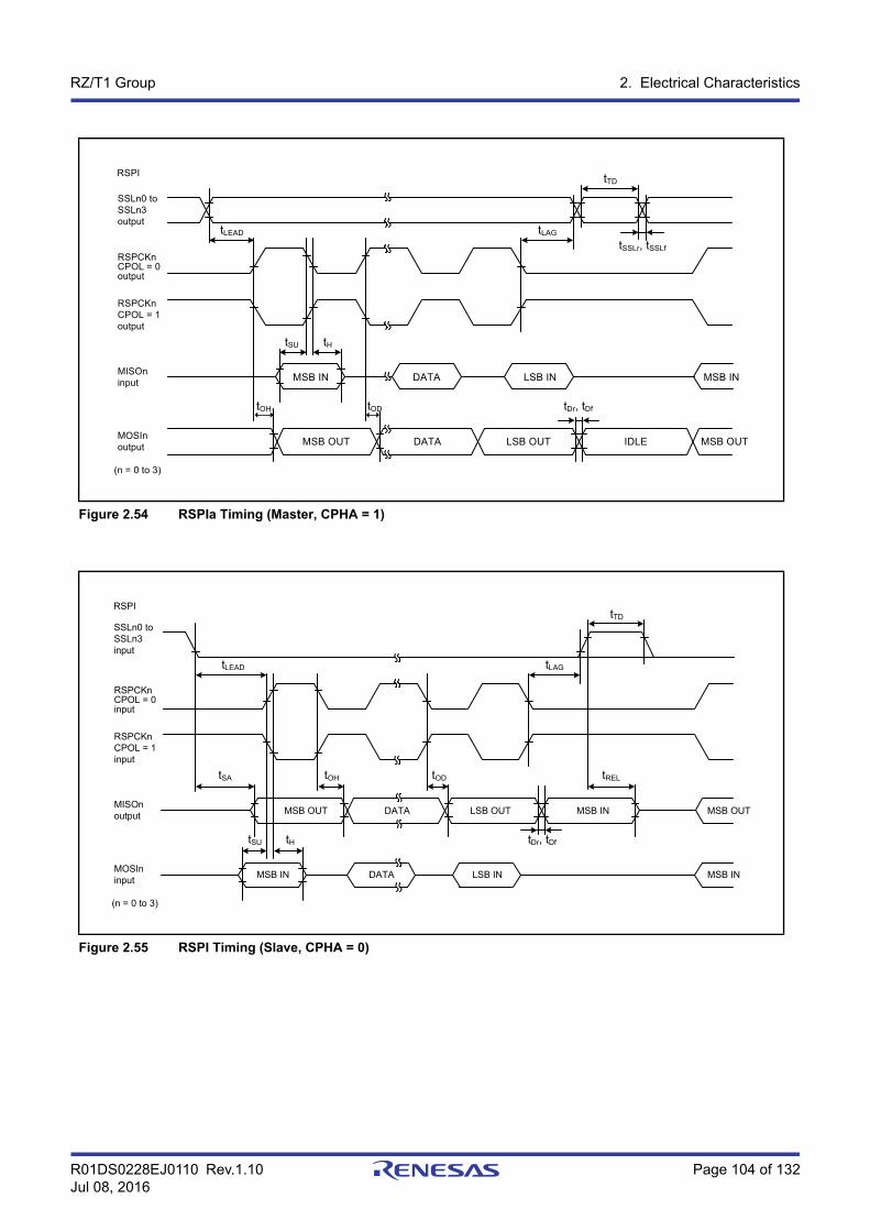
R01DS0228EJ0110 Rev.1.10 Page 104 of 132Jul 08, 2016
RZ/T1 Group 2. Electrical Characteristics
Figure 2.54 RSPIa Timing (Master, CPHA = 1)
Figure 2.55 RSPI Timing (Slave, CPHA = 0)
tSU tH
tLEAD
tTD
tLAG
tSSLr, tSSLf
tOH tOD
MSB IN DATA LSB IN MSB IN
MSB OUT DATA LSB OUT IDLE MSB OUT
SSLn0 to SSLn3output
RSPCKnCPOL = 0output
RSPCKnCPOL = 1output
MISOninput
MOSInoutput
RSPI
(n = 0 to 3)
tDr, tDf
tDr, tDftSU tH
tLEAD
tTD
tLAG
tSA
MSB IN DATA LSB IN MSB IN
MSB OUT DATA LSB OUT MSB IN MSB OUT
tOH tOD tREL
RSPCKnCPOL = 0input
RSPCKnCPOL = 1input
MISOnoutput
MOSIninput
RSPI
(n = 0 to 3)
SSLn0 to SSLn3input
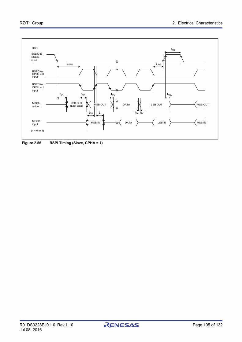
R01DS0228EJ0110 Rev.1.10 Page 105 of 132Jul 08, 2016
RZ/T1 Group 2. Electrical Characteristics
Figure 2.56 RSPI Timing (Slave, CPHA = 1)
RSPCKnCPOL = 0input
RSPCKnCPOL = 1input
MISOnoutput
MOSIninput
tDr, tDf
tSA tOH
tLEAD
tTD
tLAG
tH
LSB OUT(Last data) DATA MSB OUT
MSB IN DATA LSB IN MSB IN
LSB OUT
tSU
tOD tREL
MSB OUT
RSPI
(n = 0 to 3)
SSLn0 to SSLn3input
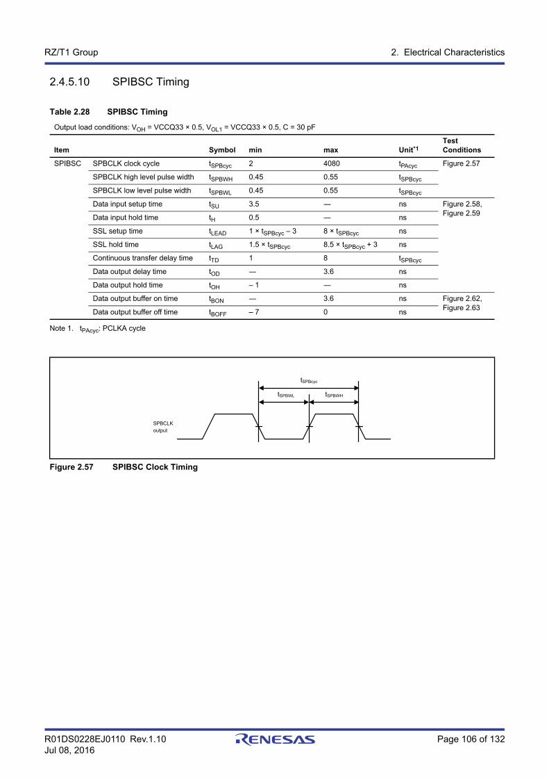
R01DS0228EJ0110 Rev.1.10 Page 106 of 132Jul 08, 2016
RZ/T1 Group 2. Electrical Characteristics
2.4.5.10 SPIBSC Timing
Note 1. tPAcyc: PCLKA cycle
Table 2.28 SPIBSC Timing
Output load conditions: VOH = VCCQ33 × 0.5, VOL1 = VCCQ33 × 0.5, C = 30 pF
Item Symbol min max Unit*1Test Conditions
SPIBSC SPBCLK clock cycle tSPBcyc 2 4080 tPAcyc Figure 2.57
SPBCLK high level pulse width tSPBWH 0.45 0.55 tSPBcyc
SPBCLK low level pulse width tSPBWL 0.45 0.55 tSPBcyc
Data input setup time tSU 3.5 ― ns Figure 2.58, Figure 2.59
Data input hold time tH 0.5 ― ns
SSL setup time tLEAD 1 × tSPBcyc – 3 8 × tSPBcyc ns
SSL hold time tLAG 1.5 × tSPBcyc 8.5 × tSPBcyc + 3 ns
Continuous transfer delay time tTD 1 8 tSPBcyc
Data output delay time tOD ― 3.6 ns
Data output hold time tOH – 1 ― ns
Data output buffer on time tBON ― 3.6 ns Figure 2.62, Figure 2.63
Data output buffer off time tBOFF – 7 0 ns
Figure 2.57 SPIBSC Clock Timing
tSPBcyc
SPBCLKoutput
tSPBWL tSPBWH
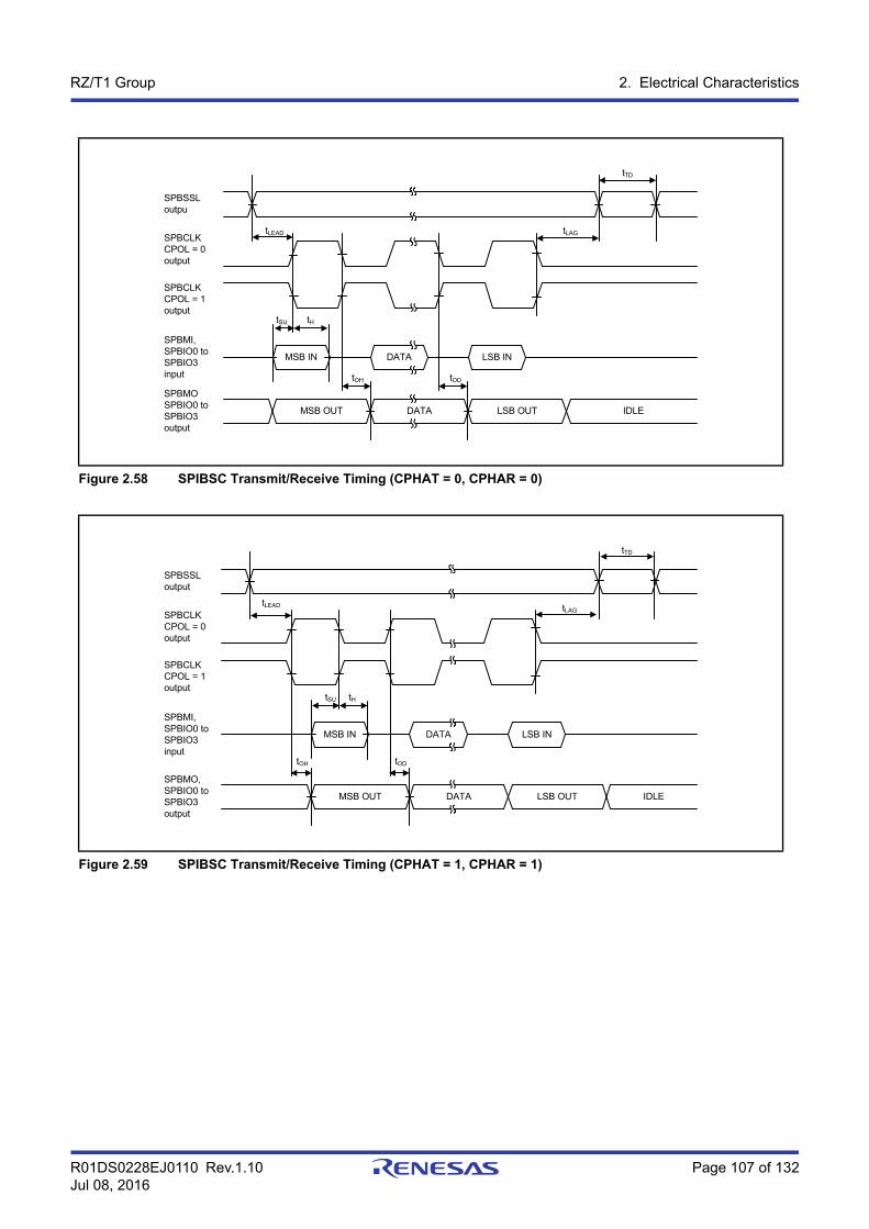
R01DS0228EJ0110 Rev.1.10 Page 107 of 132Jul 08, 2016
RZ/T1 Group 2. Electrical Characteristics
Figure 2.58 SPIBSC Transmit/Receive Timing (CPHAT = 0, CPHAR = 0)
Figure 2.59 SPIBSC Transmit/Receive Timing (CPHAT = 1, CPHAR = 1)
MSB IN
MSB OUT LSB OUT IDLE
DATA LSB IN
DATA
SPBSSLoutpu
SPBCLKCPOL = 0output
SPBCLKCPOL = 1output
SPBMI,SPBIO0 to SPBIO3input
SPBMOSPBIO0 to SPBIO3output
tLEAD tLAG
tSU tH
tOH tOD
tTD
MSB IN
MSB OUT LSB OUT IDLE
DATA LSB IN
DATA
SPBSSLoutput
SPBCLKCPOL = 0output
SPBCLKCPOL = 1output
SPBMI,SPBIO0 to SPBIO3input
SPBMO,SPBIO0 to SPBIO3output
tLEAD tLAG
tOH tOD
tTD
tSU tH
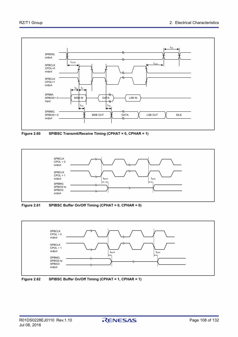
R01DS0228EJ0110 Rev.1.10 Page 108 of 132Jul 08, 2016
RZ/T1 Group 2. Electrical Characteristics
Figure 2.60 SPIBSC Transmit/Receive Timing (CPHAT = 0, CPHAR = 1)
Figure 2.61 SPIBSC Buffer On/Off Timing (CPHAT = 0, CPHAR = 0)
Figure 2.62 SPIBSC Buffer On/Off Timing (CPHAT = 1, CPHAR = 1)
MSB IN
MSB OUT LSB OUT IDLE
DATA LSB IN
DATA
SPBSSLoutput
SPBCLKCPOL=0output
SPBCLKCPOL=1output
SPBMI,SPBIO0~3input
SPBMO,SPBIO0~3output
tLEAD tLAG
tOH tOD
tTD
tSU tH
SPBCLKCPOL = 0output
SPBCLKCPOL = 1output
SPBMO,SPBIO0 to SPBIO3output
tBOFF tBON
SPBCLKCPOL = 0output
SPBCLKCPOL = 1output
SPBMO,SPBIO0 to SPBIO3output
tBOFF tBON

R01DS0228EJ0110 Rev.1.10 Page 109 of 132Jul 08, 2016
RZ/T1 Group 2. Electrical Characteristics
Figure 2.63 SPIBSC Buffer On/Off Timing (CPHAT = 0, CPHAR = 1)
SPBCLKCPOL=0output
SPBCLKCPOL=1output
SPBMO,SPBIO0~3output
tBOFF tBON

R01DS0228EJ0110 Rev.1.10 Page 110 of 132Jul 08, 2016
RZ/T1 Group 2. Electrical Characteristics
2.4.5.11 RIICa Timing
Note 1. tIICcyc: RIIC internal reference clock (IICφ) cycleNote 2. The value out of parentheses is applicable when the value of the ICMR3.NF[1:0] bits is 00b while the digital filter is enabled by
the setting ICFER.NFE = 1. The value within parentheses is applicable when the value of the ICMR3.NF[1:0] bits is 11b while the digital filter is enabled by the setting ICFER.NFE = 1.
Note 3. Cb is the total capacitance of the bus lines.Note 4. The minimum values are not specified for trs and tst in Fast-mode.
Table 2.29 RIICa Timing
Output load conditions: VOL2 = 0.4 V, IOL2 = 3 mA
Item symbol min*2 max*2 Unit*1Test Conditions
RIICa(Standard-mode)
SCL input cycle time tSCL 6(12) × tIICcyc + 1300 ― ns Figure 2.64
SCL input high pulse width tSCLH 3(6) × tIICcyc + 300 ― ns
SCL input low pulse width tSCLL 3(6) × tIICcyc + 300 ― ns
SCL, SDA input rising time tsr ― 1000 ns
SCL, SDA input falling time tsf ― 300 ns
SCL, SDA input spike pulse removal time tSP 0 1(4) × tIICcyc ns
SDA input bus free time tBUF 3(6) × tIICcyc + 300 ― ns
Start condition input hold time tSTAH tIICcyc + 300 ― ns
Restart condition input setup time tSTAS 1000 ― ns
Stop condition input setup time tSTOS 1000 ― ns
Data input setup time tSDAS tIICcyc + 50 ― ns
Data input hold time tSDAH 0 ― ns
SCL, SDA capacitive load Cb ― 400 pF
RIICa(Fast-mode)
SCL input cycle time tSCL 6(12) × tIICcyc + 600 ― ns
SCL input high pulse width tSCLH 3(6) × tIICcyc + 300 ― ns
SCL input low pulse width tSCLL 3(6) × tIICcyc + 300 ― ns
SCL, SDA input rising time tsr ―*4 300 ns
SCL, SDA input falling time tsf ―*4 300 ns
SCL, SDA input spike pulse removal time tSP 0 1(4) × tIICcyc ns
SDA input bus free time tBUF 3(6) × tIICcyc + 300 ― ns
Start condition input hold time tSTAH tIICcyc + 300 ― ns
Restart condition input setup time tSTAS 300 ― ns
Stop condition input setup time tSTOS 300 ― ns
Data input setup time tSDAS tIICcyc + 50 ― ns
Data input hold time tSDAH 0 ― ns
SCL, SDA capacitive load*3 Cb ― 400 pF
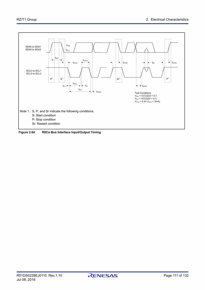
R01DS0228EJ0110 Rev.1.10 Page 111 of 132Jul 08, 2016
RZ/T1 Group 2. Electrical Characteristics
Note 1. S, P, and Sr indicate the following conditions.S: Start conditionP: Stop conditionSr: Restart condition
Figure 2.64 RIICa Bus Interface Input/Output Timing
SDA0 to SDA1SDA0 to SDA3
SCL0 to SCL1SCL0 to SCL3
VIH2
VIL2
tSTAH
tSCLH
tSCLL
P*1 S*1
tSf tSr
tSCLtSDAH
tSDAS
tSTAS tSP tSTOS
P*1
tBUF
Test ConditionsVIH2 = VCCQ33 × 0.7, VIL2 = VCCQ33 × 0.3, VOL2 = 0.4V (IOL2 = 3mA)
Sr*1

R01DS0228EJ0110 Rev.1.10 Page 112 of 132Jul 08, 2016
RZ/T1 Group 2. Electrical Characteristics
2.4.5.12 Serial Sound Interface Timing
Table 2.30 Serial Sound Interface Timing
Output load conditions: VOH = VCCQ33 × 0.5, VOL1 = VCCQ33 × 0.5, C = 30 pF
Item Symbol Min. Max. Unit Test Conditions
SSI AUDIO_CLK input frequency tAUDIO 1 50 MHz
Output clock cycle tO 150 64000 ns Figure 2.65
Input clock cycle tI 150 64000 ns
Clock high level tHC 60 ― ns
Clock low level tLC 60 ― ns
Clock rising time tRC ― 25 ns
Data delay time tDTR –5 25 ns Figure 2.66, Figure 2.67
Setup time tSR 25 ― ns
Hold time tHTR 25 ― ns
WS change edge SSITXD0 output delay TDTRW ― 25 ns Figure 2.68
Figure 2.65 Clock Input/Output Timing
Figure 2.66 Transmit/Receive Timing (SSISCK0 Rising Synchronous)
SSISCK0
tHC
tLC
tRC
tI, tO
tSR tHTR
tDTR
SSISCK0(input or output)
SSIWS0, SSIRXD0(input)
SSIWS0, SSITXD0(output)
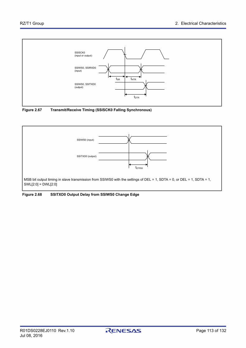
R01DS0228EJ0110 Rev.1.10 Page 113 of 132Jul 08, 2016
RZ/T1 Group 2. Electrical Characteristics
Figure 2.67 Transmit/Receive Timing (SSISCK0 Falling Synchronous)
MSB bit output timing in slave transmission from SSIWS0 with the settings of DEL = 1, SDTA = 0, or DEL = 1, SDTA = 1, SWL[2:0] = DWL[2:0]
Figure 2.68 SSITXD0 Output Delay from SSIWS0 Change Edge
tSR tHTR
tDTR
SSISCK0(input or output)
SSIWS0, SSIRXD0(input)
SSIWS0, SSITXD0(output)
tDTRW
SSIWS0 (input)
SSITXD0 (output)

R01DS0228EJ0110 Rev.1.10 Page 114 of 132Jul 08, 2016
RZ/T1 Group 2. Electrical Characteristics
2.4.5.13 CAN Interface Timing
Internal delay time (tnode) = Internal transmission delay time (toutput) + Internal reception delay time (tinput)
Table 2.31 CAN Interface Timing
Item Symbol min max Unit Test Conditions
Internal delay time tnode ― 100 ns Figure 2.69
Transmission rate ― 1 Mbps
Figure 2.69 CAN Interface Conditions
CAN controller
Internal transmission delay time(toutput)
Internal reception delay time(tinput)
CTXD0, CTXD1 pins
CRXD0, CRXD1 pins
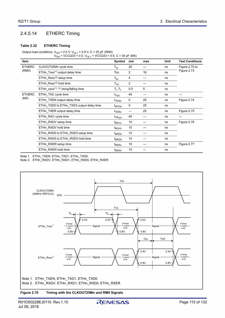
R01DS0228EJ0110 Rev.1.10 Page 115 of 132Jul 08, 2016
RZ/T1 Group 2. Electrical Characteristics
2.4.5.14 ETHERC Timing
Note 1. ETHn_TXEN, ETHn_TXD1, ETHn_TXD0Note 2. ETHn_RXDV, ETHn_RXD1, ETHn_RXD0, ETHn_RXER
Table 2.32 ETHERC Timing
Output load conditions: VOH = 2.0 V, VOL1 = 0.8 V, C = 25 pF (RMII) VOH = VCCQ33 × 0.5, VOL1 = VCCQ33 × 0.5, C = 30 pF (MII)
Item Symbol min max Unit Test Conditions
ETHERC(RMII)
CLKOUT25Mn cycle time Tck 20 ― ns Figure 2.70 to Figure 2.73
ETHn_Txxx*1 output delay time Tco 2 16 ns
ETHn_Rxxx*2 setup time Tsu 4 ― ns
ETHn_Rxxx*2 hold time Thd 2 ― ns
ETHn_xxxx*1, *2 rising/falling time Tr, Tf 0.5 5 ns
ETHERC(MII)
ETHn_TXC cycle time tTcyc 40 ― ns ―
ETHn_TXEN output delay time tTENd 0 25 ns Figure 2.74
ETHn_TXD0 to ETHn_TXD3 output delay time tMTDd 0 25 ns
ETHn_TXER output delay time tTERd ― 25 ns Figure 2.75
ETHn_RXC cycle time tTRcyc 40 ― ns ―
ETHn_RXDV setup time tRDVs 10 ― ns Figure 2.76
ETHn_RXDV hold time tRDVh 10 ― ns
ETHn_RXD0 to ETHn_RXD3 setup time tMRDs 10 ― ns
ETHn_RXD0 to ETHn_RXD3 hold time tMRDh 10 ― ns
ETHn_RXER setup time tRERs 10 ― ns Figure 2.77
ETHn_RXER hold time tRERh 10 ― ns
Note 1. ETHn_TXEN, ETHn_TXD1, ETHn_TXD0Note 2. ETHn_RXDV, ETHn_RXD1, ETHn_RXD0, ETHn_RXER
Figure 2.70 Timing with the CLKOUT25Mn and RMII Signals
Tck
Tco
CLKOUT25Mn(50MHz REFCLK)
ETHn_Txxx*1
50%
0.8V
Tr Tf
ETHn_Rxxx*2
2.4V
0.8V
Tsu Thd
Signal Signal
Signal Signal
0.8V 0.8V
2.0V 2.0V 2.0V
0.8V
2.4V
Change in signal
level
Change in signal
level
Change in signal
level
Change in signal
level
Change in signal
level
Change in signal
level
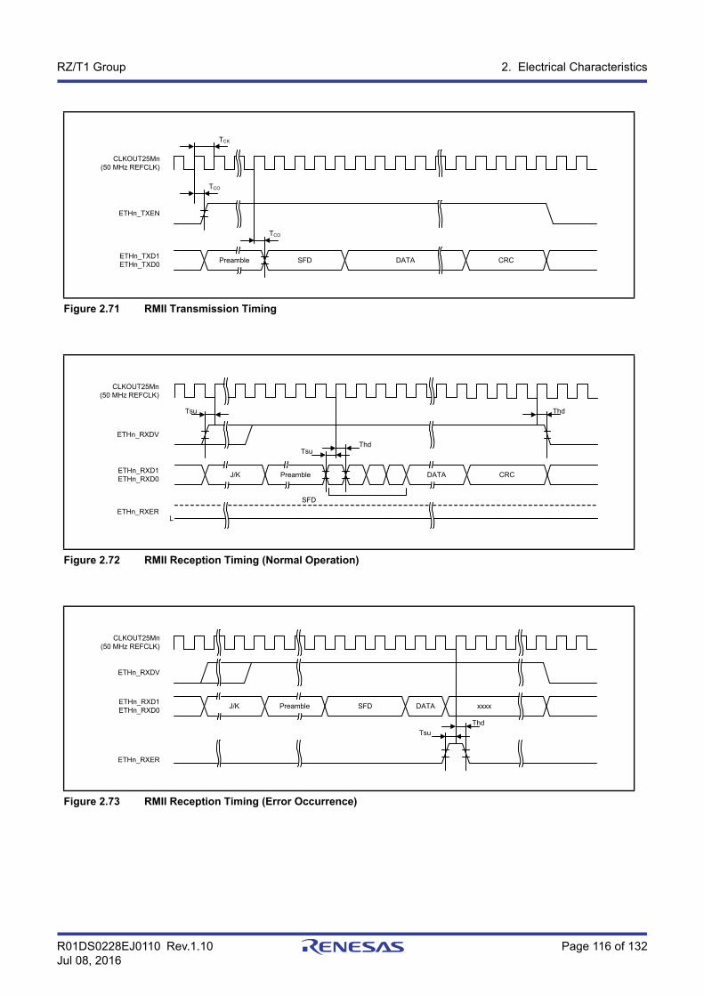
R01DS0228EJ0110 Rev.1.10 Page 116 of 132Jul 08, 2016
RZ/T1 Group 2. Electrical Characteristics
Figure 2.71 RMII Transmission Timing
Figure 2.72 RMII Reception Timing (Normal Operation)
Figure 2.73 RMII Reception Timing (Error Occurrence)
Preamble SFD DATA CRC
TCO
TCO
TCK
CLKOUT25Mn(50 MHz REFCLK)
ETHn_TXEN
ETHn_TXD1ETHn_TXD0
J/K DATA CRC
SFD
Tsu
TsuThd
Thd
L
ETHn_RXDV
ETHn_RXD1ETHn_RXD0
ETHn_RXER
CLKOUT25Mn(50 MHz REFCLK)
Preamble
Preamble DATASFD xxxx
Tsu
Thd
CLKOUT25Mn(50 MHz REFCLK)
ETHn_RXDV
ETHn_RXD1ETHn_RXD0
ETHn_RXER
J/K
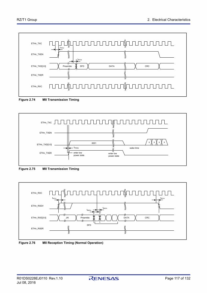
R01DS0228EJ0110 Rev.1.10 Page 117 of 132Jul 08, 2016
RZ/T1 Group 2. Electrical Characteristics
Figure 2.74 MII Transmission Timing
Figure 2.75 MII Transmission Timing
Figure 2.76 MII Reception Timing (Normal Operation)
ETHn_TXC
ETHn_TXEN
ETHn_TXD[3:0]
ETHn_TXER
SFD DATA CRCPreamble
tTENd
tMTDd
ETHn_RXC
ETHn_TXC
ETHn_TXEN
ETHn_TXD[3:0]
ETHn_TXER enter lowpower state
0001
tTERd
enter lowpower state
wake time
x x x x
ETHn_RXC
ETHn_RXDV
ETHn_RXD[3:0]
ETHn_RXER
J/K DATA CRC
SFD
Preamble
tRDVs tRDVh
tMRDs
tMRDh
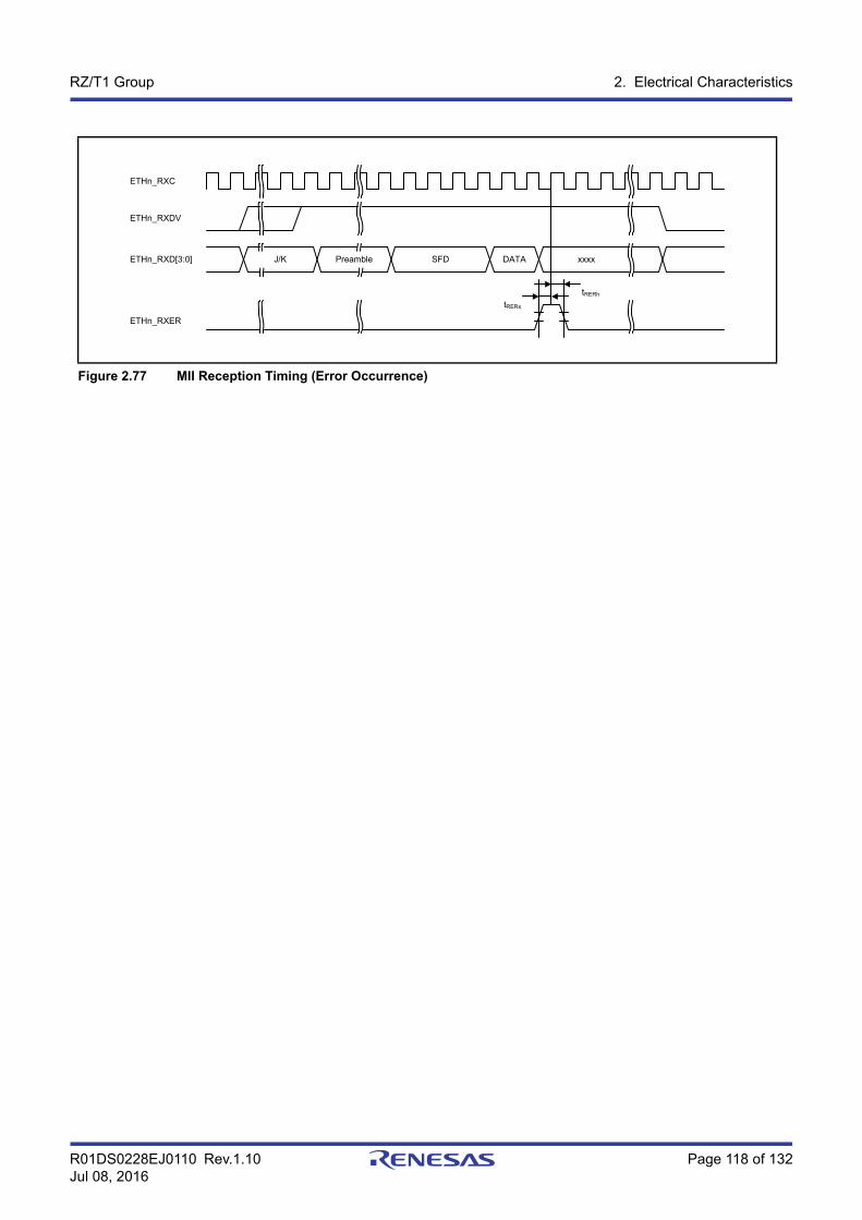
R01DS0228EJ0110 Rev.1.10 Page 118 of 132Jul 08, 2016
RZ/T1 Group 2. Electrical Characteristics
Figure 2.77 MII Reception Timing (Error Occurrence)
ETHn_RXC
ETHn_RXDV
ETHn_RXD[3:0]
ETHn_RXER
Preamble DATASFD xxxxJ/K
tRERs
tRERh

R01DS0228EJ0110 Rev.1.10 Page 119 of 132Jul 08, 2016
RZ/T1 Group 2. Electrical Characteristics
2.4.5.15 Serial Management Interface
Table 2.33 Serial Management Interface
Output load conditions: VOH = VCCQ33 × 0.5, VOL1 = VCCQ33 × 0.5, C = 30 pF
Item Symbol min max UnitTest Conditions
MDIO ETHn_MDC output cycle tMDC 80 ― ns Figure 2.78
ETHn_MDIO input setting time (to ETHn_MDC↑) tSMDIO 10 ― ns
ETHn_MDIO input hold time (to ETHn_MDC↑) tHMDIO 0 ― ns
ETHn_MDIO output delay time (to ETHn_MDC↓) tDMDIO ― 20 ns
Figure 2.78 Serial Management Access Timing
ETH_MDC(Output)
ETH_MDIO(Input)
tMDC
tHMDIO
ETH_MDIO(Output)
tDMDIO tDMDIO
tSMDIO

R01DS0228EJ0110 Rev.1.10 Page 120 of 132Jul 08, 2016
RZ/T1 Group 2. Electrical Characteristics
2.4.5.16 Delta-Sigma Interface Timing
Note: tDCcyc: One cycle time of the ∆Σ interface clock (DSCLK0, DSCLK1)
Table 2.34 ∆Σ Interface Timing
Conditions: VOH = VCCQ33 × 0.5, VOL1 = VCCQ33 × 0.5, C = 30 pF
Item Symbol min max UnitTest Conditions
DSMIF Clock cycle Master tDScyc 1 1 tDCcyc Figure 2.79
Slave 40 200 ns
Clock high level Master tDSCKWH 16 ― ns
Slave 16 ― ns
Clock low level Master tDSCKWL 16 ― ns
Slave 16 ― ns
Setup time Master tSU 15 ― ns Figure 2.80,Figure 2.81
Slave 10 ― ns
Hold time Master tH 0 ― ns
Slave 10 ― ns
Figure 2.79 Clock Input/Output Timing
Figure 2.80 Reception Timing (MCLKn Rising Synchronous)
MCLKn
tDSCKWH
tDSCKWL
tDScyc
tSU tH
MCLKn(input or output)
MDATn(input)

R01DS0228EJ0110 Rev.1.10 Page 121 of 132Jul 08, 2016
RZ/T1 Group 2. Electrical Characteristics
Figure 2.81 Reception Timing (MCLKn Falling Synchronous)
tSU tH
MCLKn(input or output)
MDATn(input)
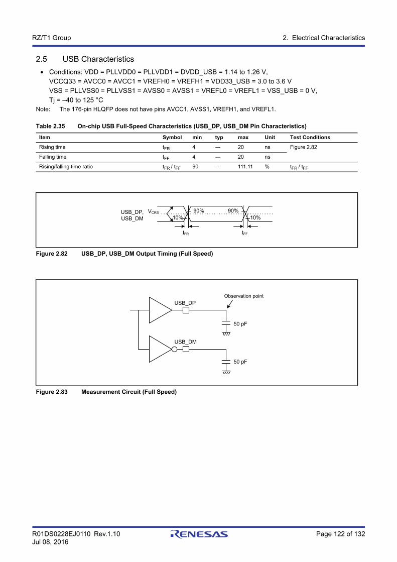
R01DS0228EJ0110 Rev.1.10 Page 122 of 132Jul 08, 2016
RZ/T1 Group 2. Electrical Characteristics
2.5 USB Characteristics
• Conditions: VDD = PLLVDD0 = PLLVDD1 = DVDD_USB = 1.14 to 1.26 V,
VCCQ33 = AVCC0 = AVCC1 = VREFH0 = VREFH1 = VDD33_USB = 3.0 to 3.6 V
VSS = PLLVSS0 = PLLVSS1 = AVSS0 = AVSS1 = VREFL0 = VREFL1 = VSS_USB = 0 V,
Tj = –40 to 125 °CNote: The 176-pin HLQFP does not have pins AVCC1, AVSS1, VREFH1, and VREFL1.
Table 2.35 On-chip USB Full-Speed Characteristics (USB_DP, USB_DM Pin Characteristics)
Item Symbol min typ max Unit Test Conditions
Rising time tFR 4 ― 20 ns Figure 2.82
Falling time tFF 4 ― 20 ns
Rising/falling time ratio tFR / tFF 90 ― 111.11 % tFR / tFF
Figure 2.82 USB_DP, USB_DM Output Timing (Full Speed)
Figure 2.83 Measurement Circuit (Full Speed)
USB_DP, USB_DM
tFFtFR
90%10%10%
90%VCRS
Observation point
50 pF
50 pF
USB_DP
USB_DM
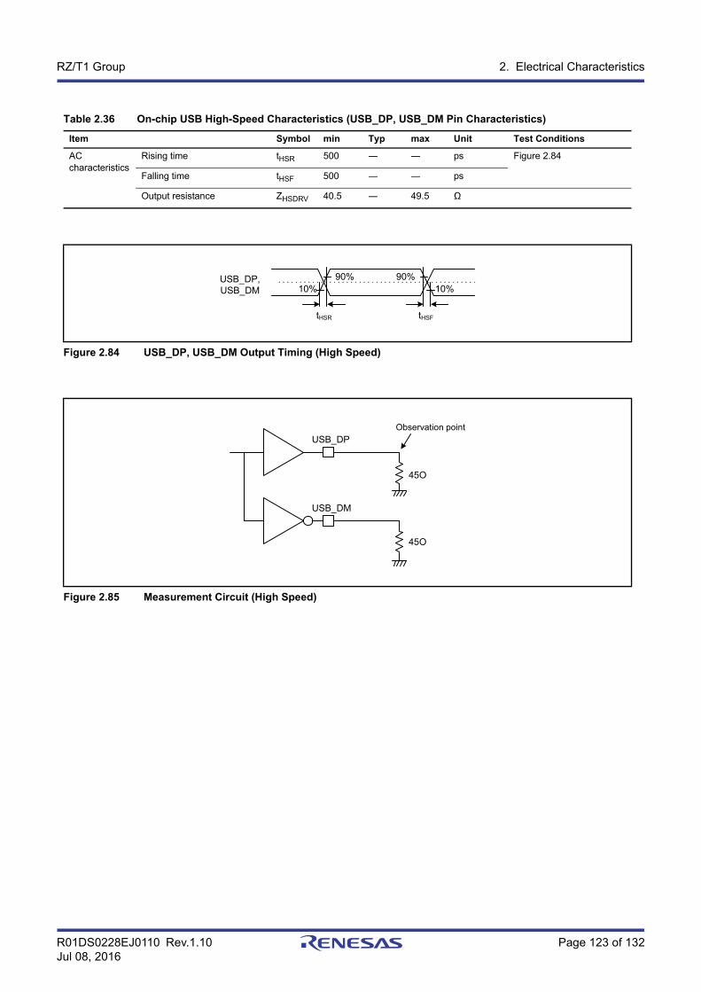
R01DS0228EJ0110 Rev.1.10 Page 123 of 132Jul 08, 2016
RZ/T1 Group 2. Electrical Characteristics
Table 2.36 On-chip USB High-Speed Characteristics (USB_DP, USB_DM Pin Characteristics)
Item Symbol min Typ max Unit Test Conditions
AC characteristics
Rising time tHSR 500 ― ― ps Figure 2.84
Falling time tHSF 500 ― ― ps
Output resistance ZHSDRV 40.5 ― 49.5 Ω
Figure 2.84 USB_DP, USB_DM Output Timing (High Speed)
Figure 2.85 Measurement Circuit (High Speed)
USB_DP, USB_DM
tHSFtHSR
90%10%10%
90%
Observation point
USB_DP
USB_DM
45O
45O
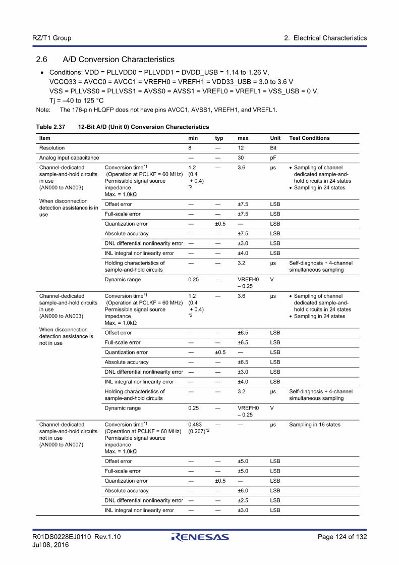
R01DS0228EJ0110 Rev.1.10 Page 124 of 132Jul 08, 2016
RZ/T1 Group 2. Electrical Characteristics
2.6 A/D Conversion Characteristics
• Conditions: VDD = PLLVDD0 = PLLVDD1 = DVDD_USB = 1.14 to 1.26 V,
VCCQ33 = AVCC0 = AVCC1 = VREFH0 = VREFH1 = VDD33_USB = 3.0 to 3.6 V
VSS = PLLVSS0 = PLLVSS1 = AVSS0 = AVSS1 = VREFL0 = VREFL1 = VSS_USB = 0 V,
Tj = –40 to 125 °CNote: The 176-pin HLQFP does not have pins AVCC1, AVSS1, VREFH1, and VREFL1.
Table 2.37 12-Bit A/D (Unit 0) Conversion Characteristics
Item min typ max Unit Test Conditions
Resolution 8 ― 12 Bit
Analog input capacitance ― ― 30 pF
Channel-dedicated sample-and-hold circuits in use(AN000 to AN003)
When disconnection detection assistance is in use
Conversion time*1
(Operation at PCLKF = 60 MHz)Permissible signal source impedanceMax. = 1.0kΩ
1.2(0.4 + 0.4)*2
― 3.6 μs • Sampling of channel dedicated sample-and-hold circuits in 24 states
• Sampling in 24 states
Offset error ― ― ±7.5 LSB
Full-scale error ― ― ±7.5 LSB
Quantization error ― ±0.5 ― LSB
Absolute accuracy ― ― ±7.5 LSB
DNL differential nonlinearity error ― ― ±3.0 LSB
INL integral nonlinearity error ― ― ±4.0 LSB
Holding characteristics of sample-and-hold circuits
― ― 3.2 μs Self-diagnosis + 4-channel simultaneous sampling
Dynamic range 0.25 ― VREFH0 – 0.25
V
Channel-dedicated sample-and-hold circuits in use(AN000 to AN003)
When disconnection detection assistance is not in use
Conversion time*1
(Operation at PCLKF = 60 MHz)Permissible signal source impedanceMax. = 1.0kΩ
1.2(0.4 + 0.4)*2
― 3.6 μs • Sampling of channel dedicated sample-and-hold circuits in 24 states
• Sampling in 24 states
Offset error ― ― ±6.5 LSB
Full-scale error ― ― ±6.5 LSB
Quantization error ― ±0.5 ― LSB
Absolute accuracy ― ― ±6.5 LSB
DNL differential nonlinearity error ― ― ±3.0 LSB
INL integral nonlinearity error ― ― ±4.0 LSB
Holding characteristics of sample-and-hold circuits
― ― 3.2 μs Self-diagnosis + 4-channel simultaneous sampling
Dynamic range 0.25 ― VREFH0 – 0.25
V
Channel-dedicated sample-and-hold circuits not in use(AN000 to AN007)
Conversion time*1
(Operation at PCLKF = 60 MHz)Permissible signal source impedanceMax. = 1.0kΩ
0.483(0.267)*2
― ― μs Sampling in 16 states
Offset error ― ― ±5.0 LSB
Full-scale error ― ― ±5.0 LSB
Quantization error ― ±0.5 ― LSB
Absolute accuracy ― ― ±6.0 LSB
DNL differential nonlinearity error ― ― ±2.5 LSB
INL integral nonlinearity error ― ― ±3.0 LSB
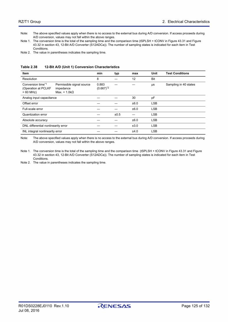
R01DS0228EJ0110 Rev.1.10 Page 125 of 132Jul 08, 2016
RZ/T1 Group 2. Electrical Characteristics
Note: The above specified values apply when there is no access to the external bus during A/D conversion. If access proceeds during A/D conversion, values may not fall within the above ranges.
Note 1. The conversion time is the total of the sampling time and the comparison time (tSPLSH + tCONV in Figure 43.31 and Figure 43.32 in section 43, 12-Bit A/D Converter (S12ADCa)). The number of sampling states is indicated for each item in Test Conditions.
Note 2. The value in parentheses indicates the sampling time.
Table 2.38 12-Bit A/D (Unit 1) Conversion Characteristics
Item min typ max Unit Test Conditions
Resolution 8 ― 12 Bit
Conversion time*1
(Operation at PCLKF = 60 MHz)
Permissible signal source impedanceMax. = 1.0kΩ
0.883(0.667)*2
― ― μs Sampling in 40 states
Analog input capacitance ― ― 30 pF
Offset error ― ― ±6.0 LSB
Full-scale error ― ― ±6.0 LSB
Quantization error ― ±0.5 ― LSB
Absolute accuracy ― ― ±6.0 LSB
DNL differential nonlinearity error ― ― ±3.0 LSB
INL integral nonlinearity error ― ― ±4.0 LSB
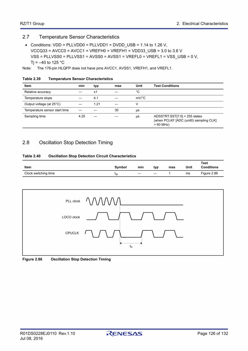
R01DS0228EJ0110 Rev.1.10 Page 126 of 132Jul 08, 2016
RZ/T1 Group 2. Electrical Characteristics
2.7 Temperature Sensor Characteristics
• Conditions: VDD = PLLVDD0 = PLLVDD1 = DVDD_USB = 1.14 to 1.26 V,
VCCQ33 = AVCC0 = AVCC1 = VREFH0 = VREFH1 = VDD33_USB = 3.0 to 3.6 V
VSS = PLLVSS0 = PLLVSS1 = AVSS0 = AVSS1 = VREFL0 = VREFL1 = VSS_USB = 0 V,
Tj = –40 to 125 °CNote: The 176-pin HLQFP does not have pins AVCC1, AVSS1, VREFH1, and VREFL1.
2.8 Oscillation Stop Detection Timing
Table 2.39 Temperature Sensor Characteristics
Item min typ max Unit Test Conditions
Relative accuracy ― ±1 ― °C
Temperature slope ― 4.1 ― mV/°C
Output voltage (at 25°C) ― 1.21 ― V
Temperature sensor start time ― ― 30 μs
Sampling time 4.25 ― ― μs ADSSTRT.SST[7:0] = 255 states(when PCLKF [ADC (unit0) sampling CLK] = 60 MHz)
Table 2.40 Oscillation Stop Detection Circuit Characteristics
Item Symbol min typ max UnitTest Conditions
Clock switching time tdr ― ― 1 ms Figure 2.86
Figure 2.86 Oscillation Stop Detection Timing
PLL clock
CPUCLK
LOCO clock
tdr
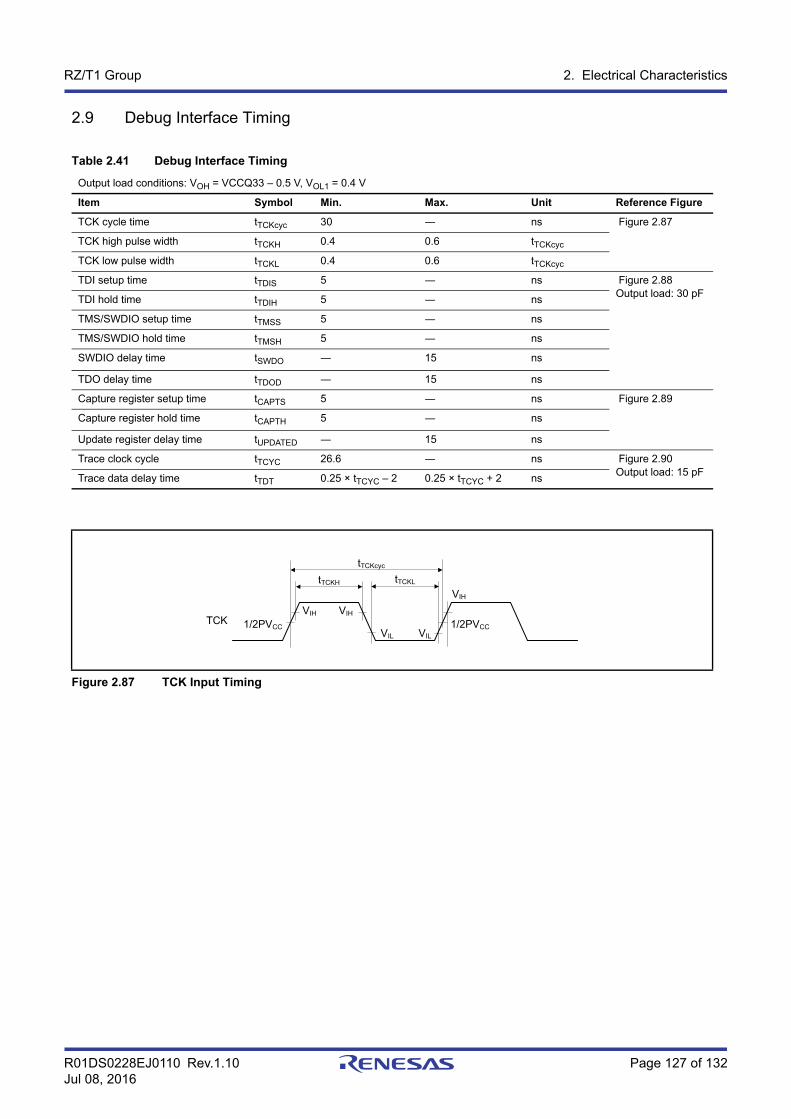
R01DS0228EJ0110 Rev.1.10 Page 127 of 132Jul 08, 2016
RZ/T1 Group 2. Electrical Characteristics
2.9 Debug Interface Timing
Table 2.41 Debug Interface Timing
Output load conditions: VOH = VCCQ33 – 0.5 V, VOL1 = 0.4 V
Item Symbol Min. Max. Unit Reference Figure
TCK cycle time tTCKcyc 30 ― ns Figure 2.87
TCK high pulse width tTCKH 0.4 0.6 tTCKcyc
TCK low pulse width tTCKL 0.4 0.6 tTCKcyc
TDI setup time tTDIS 5 ― ns Figure 2.88Output load: 30 pF
TDI hold time tTDIH 5 ― ns
TMS/SWDIO setup time tTMSS 5 ― ns
TMS/SWDIO hold time tTMSH 5 ― ns
SWDIO delay time tSWDO ― 15 ns
TDO delay time tTDOD ― 15 ns
Capture register setup time tCAPTS 5 ― ns Figure 2.89
Capture register hold time tCAPTH 5 ― ns
Update register delay time tUPDATED ― 15 ns
Trace clock cycle tTCYC 26.6 ― ns Figure 2.90Output load: 15 pF
Trace data delay time tTDT 0.25 × tTCYC – 2 0.25 × tTCYC + 2 ns
Figure 2.87 TCK Input Timing
tTCKcyc
tTCKH tTCKL
TCKVIH VIH
VIL VIL
1/2PVCC1/2PVCC
VIH
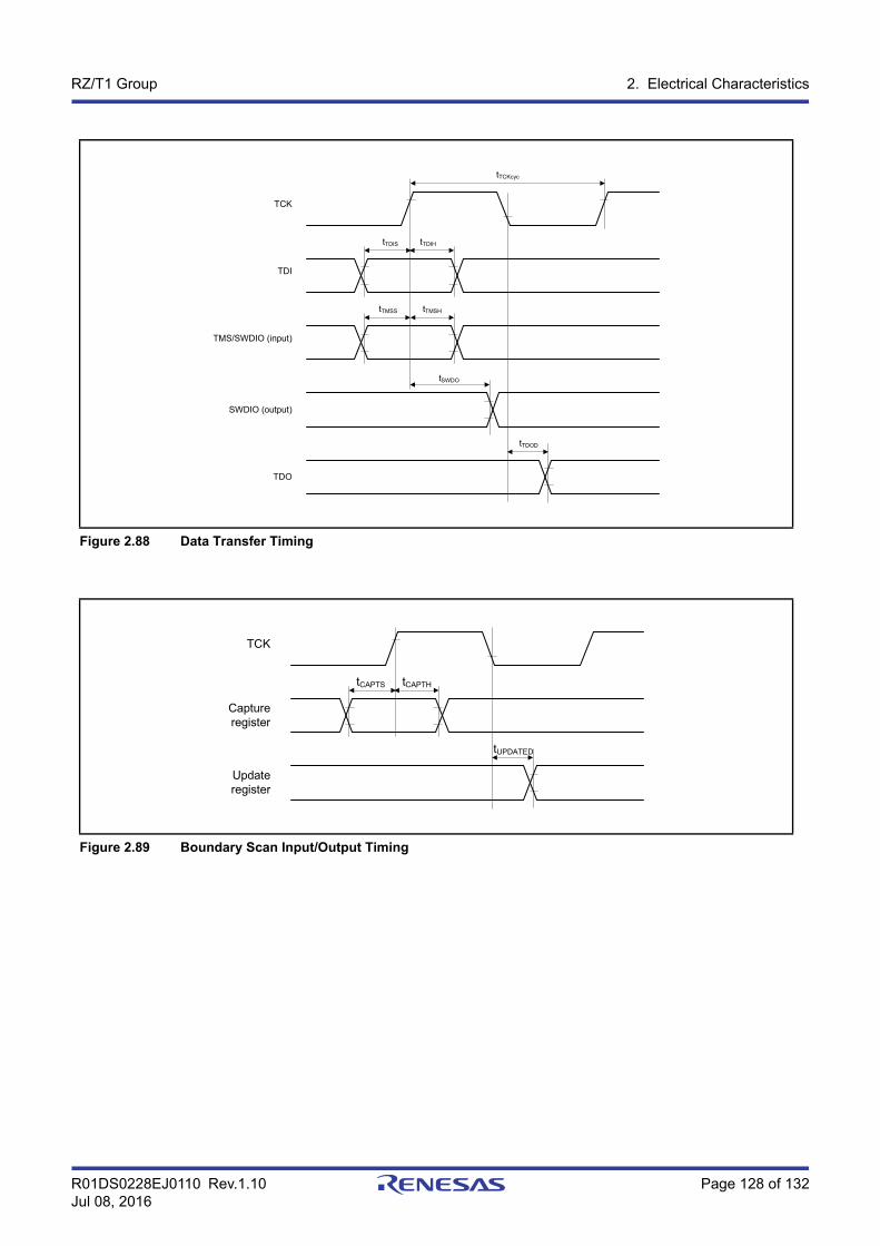
R01DS0228EJ0110 Rev.1.10 Page 128 of 132Jul 08, 2016
RZ/T1 Group 2. Electrical Characteristics
Figure 2.88 Data Transfer Timing
Figure 2.89 Boundary Scan Input/Output Timing
tSWDO
tTDOD
SWDIO (output)
TDO
tTMSS tTMSH
TMS/SWDIO (input)
tTDIS tTDIH
TDI
tTCKcyc
TCK
tCAPTS tCAPTH
Capture register
TCK
tUPDATED
Update register
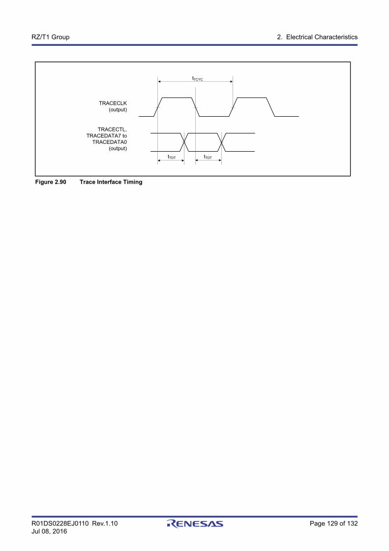
R01DS0228EJ0110 Rev.1.10 Page 129 of 132Jul 08, 2016
RZ/T1 Group 2. Electrical Characteristics
Figure 2.90 Trace Interface Timing
tTCYC
TRACECLK(output)
tTDT tTDT
TRACECTL,TRACEDATA7 to
TRACEDATA0(output)
RZ/T1 Group 改定記録
R01DS0228EJ0110 Rev.1.10 Page 130 of 132Jul 08, 2016
REVISION HISTORY RZ/T1 Group Datasheet
Rev. Date
Description
Page Summary
0.60 Nov 14, 2014 ― First edition, issued
0.70 Dec.25, 2014 Features
1 Operating temperature range: Heading title and description corrected
Section 1 Overview
11 Table 1.3 List of Products (2 / 2): Note corrected
21 Figure 1.3 Pin Arrangement (176-pin HLQFP): The names of pins 33, 34, 38, 39, and 91, corrected
26 Table 1.5 Pin Assignments (320-Pin FBGA) (5 / 8): The names of pins M20 and P19, corrected
27 Table 1.5 Pin Assignments (320-Pin FBGA) (6 / 8): The names of pins R14, R19, R20, T9, V7, and V8, corrected
29 Table 1.5 Pin Assignments (320-Pin FBGA) (8 / 8): The names of pins Y16 and Y17, corrected
30 Table 1.6 Pin Assignments (176-Pin HLQFP) (1 / 4): The names of pins 33, 34, 38, and 39, corrected
31 Table 1.6 Pin Assignments (176-Pin HLQFP) (2 / 4): The names of pins 58, 59, 60, 79, 82, and 83, corrected
32 Table 1.6 Pin Assignments (176-Pin HLQFP) (3 / 4): The names of pins 91 and 110, corrected
33 Table 1.6 Pin Assignments (176-Pin HLQFP) (4 / 4): The names of pins 136, 153, 154, 155, 156, and 157, corrected
39 Table 1.7 List of Pin and Pin Functions (320-Pin FBGA) (6 / 10): The name of pin M20, corrected
40 Table 1.7 List of Pin and Pin Functions (320-Pin FBGA) (7 / 10): The names of pins P19, R8, and R14, corrected
41 Table 1.7 List of Pin and Pin Functions (320-Pin FBGA) (8 / 10): The names of pins R19, R20, T9, V7, and V8, corrected
42 Table 1.7 List of Pin and Pin Functions (320-Pin FBGA) (9 / 10): The names of pins Y16 and Y17, corrected
1.10 Jul.08, 2016 Feature
1 Wholly amended
1. Overview
2 to 49 Wholly amended
2. Electrical Characteristics
50 to 129 Newly added
REVISION HISTORY

General Precautions in the Handling of MPU/MCU Products
The following usage notes are applicable to all MPU/MCU products from Renesas. For detailed usage notes on the products covered by this document, refer to the relevant sections of the document as well as any technical updates that have been issued for the products.
1. Handling of Unused Pins Handle unused pins in accordance with the directions given under Handling of Unused Pins in the manual. ⎯ The input pins of CMOS products are generally in the high-impedance state. In operation with an
unused pin in the open-circuit state, extra electromagnetic noise is induced in the vicinity of LSI, an associated shoot-through current flows internally, and malfunctions occur due to the false recognition of the pin state as an input signal become possible. Unused pins should be handled as described under Handling of Unused Pins in the manual.
2. Processing at Power-on The state of the product is undefined at the moment when power is supplied. ⎯ The states of internal circuits in the LSI are indeterminate and the states of register settings and
pins are undefined at the moment when power is supplied. In a finished product where the reset signal is applied to the external reset pin, the states of pins are not guaranteed from the moment when power is supplied until the reset process is completed. In a similar way, the states of pins in a product that is reset by an on-chip power-on reset function are not guaranteed from the moment when power is supplied until the power reaches the level at which resetting has been specified.
3. Prohibition of Access to Reserved Addresses Access to reserved addresses is prohibited. ⎯ The reserved addresses are provided for the possible future expansion of functions. Do not access
these addresses; the correct operation of LSI is not guaranteed if they are accessed. 4. Clock Signals
After applying a reset, only release the reset line after the operating clock signal has become stable. When switching the clock signal during program execution, wait until the target clock signal has stabilized. ⎯ When the clock signal is generated with an external resonator (or from an external oscillator)
during a reset, ensure that the reset line is only released after full stabilization of the clock signal. Moreover, when switching to a clock signal produced with an external resonator (or by an external oscillator) while program execution is in progress, wait until the target clock signal is stable.
5. Differences between Products Before changing from one product to another, i.e. to a product with a different part number, confirm that the change will not lead to problems. ⎯ The characteristics of an MPU or MCU in the same group but having a different part number may
differ in terms of the internal memory capacity, layout pattern, and other factors, which can affect the ranges of electrical characteristics, such as characteristic values, operating margins, immunity to noise, and amount of radiated noise. When changing to a product with a different part number, implement a system-evaluation test for the given product.
General Precautions in the Handling of MPU/MCU Products

NoticeNotice
1. Descriptions of circuits, software and other related information in this document are provided only to illustrate the operation of semiconductor products and application examples. You are fully responsible for
the incorporation of these circuits, software, and information in the design of your equipment. Renesas Electronics assumes no responsibility for any losses incurred by you or third parties arising from the
use of these circuits, software, or information.
2. Renesas Electronics has used reasonable care in preparing the information included in this document, but Renesas Electronics does not warrant that such information is error free. Renesas Electronics
assumes no liability whatsoever for any damages incurred by you resulting from errors in or omissions from the information included herein.
3. Renesas Electronics does not assume any liability for infringement of patents, copyrights, or other intellectual property rights of third parties by or arising from the use of Renesas Electronics products or
technical information described in this document. No license, express, implied or otherwise, is granted hereby under any patents, copyrights or other intellectual property rights of Renesas Electronics or
others.
4. You should not alter, modify, copy, or otherwise misappropriate any Renesas Electronics product, whether in whole or in part. Renesas Electronics assumes no responsibility for any losses incurred by you or
third parties arising from such alteration, modification, copy or otherwise misappropriation of Renesas Electronics product.
5. Renesas Electronics products are classified according to the following two quality grades: "Standard" and "High Quality". The recommended applications for each Renesas Electronics product depends on
the product's quality grade, as indicated below.
"Standard": Computers; office equipment; communications equipment; test and measurement equipment; audio and visual equipment; home electronic appliances; machine tools; personal electronic
equipment; and industrial robots etc.
"High Quality": Transportation equipment (automobiles, trains, ships, etc.); traffic control systems; anti-disaster systems; anti-crime systems; and safety equipment etc.
Renesas Electronics products are neither intended nor authorized for use in products or systems that may pose a direct threat to human life or bodily injury (artificial life support devices or systems, surgical
implantations etc.), or may cause serious property damages (nuclear reactor control systems, military equipment etc.). You must check the quality grade of each Renesas Electronics product before using it
in a particular application. You may not use any Renesas Electronics product for any application for which it is not intended. Renesas Electronics shall not be in any way liable for any damages or losses
incurred by you or third parties arising from the use of any Renesas Electronics product for which the product is not intended by Renesas Electronics.
6. You should use the Renesas Electronics products described in this document within the range specified by Renesas Electronics, especially with respect to the maximum rating, operating supply voltage
range, movement power voltage range, heat radiation characteristics, installation and other product characteristics. Renesas Electronics shall have no liability for malfunctions or damages arising out of the
use of Renesas Electronics products beyond such specified ranges.
7. Although Renesas Electronics endeavors to improve the quality and reliability of its products, semiconductor products have specific characteristics such as the occurrence of failure at a certain rate and
malfunctions under certain use conditions. Further, Renesas Electronics products are not subject to radiation resistance design. Please be sure to implement safety measures to guard them against the
possibility of physical injury, and injury or damage caused by fire in the event of the failure of a Renesas Electronics product, such as safety design for hardware and software including but not limited to
redundancy, fire control and malfunction prevention, appropriate treatment for aging degradation or any other appropriate measures. Because the evaluation of microcomputer software alone is very difficult,
please evaluate the safety of the final products or systems manufactured by you.
8. Please contact a Renesas Electronics sales office for details as to environmental matters such as the environmental compatibility of each Renesas Electronics product. Please use Renesas Electronics
products in compliance with all applicable laws and regulations that regulate the inclusion or use of controlled substances, including without limitation, the EU RoHS Directive. Renesas Electronics assumes
no liability for damages or losses occurring as a result of your noncompliance with applicable laws and regulations.
9. Renesas Electronics products and technology may not be used for or incorporated into any products or systems whose manufacture, use, or sale is prohibited under any applicable domestic or foreign laws or
regulations. You should not use Renesas Electronics products or technology described in this document for any purpose relating to military applications or use by the military, including but not limited to the
development of weapons of mass destruction. When exporting the Renesas Electronics products or technology described in this document, you should comply with the applicable export control laws and
regulations and follow the procedures required by such laws and regulations.
10. It is the responsibility of the buyer or distributor of Renesas Electronics products, who distributes, disposes of, or otherwise places the product with a third party, to notify such third party in advance of the
contents and conditions set forth in this document, Renesas Electronics assumes no responsibility for any losses incurred by you or third parties as a result of unauthorized use of Renesas Electronics
products.
11. This document may not be reproduced or duplicated in any form, in whole or in part, without prior written consent of Renesas Electronics.
12. Please contact a Renesas Electronics sales office if you have any questions regarding the information contained in this document or Renesas Electronics products, or if you have any other inquiries.
(Note 1) "Renesas Electronics" as used in this document means Renesas Electronics Corporation and also includes its majority-owned subsidiaries.
(Note 2) "Renesas Electronics product(s)" means any product developed or manufactured by or for Renesas Electronics.
http://www.renesas.comRefer to "http://www.renesas.com/" for the latest and detailed information.
Renesas Electronics America Inc.2801 Scott Boulevard Santa Clara, CA 95050-2549, U.S.A.Tel: +1-408-588-6000, Fax: +1-408-588-6130Renesas Electronics Canada Limited1101 Nicholson Road, Newmarket, Ontario L3Y 9C3, CanadaTel: +1-905-898-5441, Fax: +1-905-898-3220Renesas Electronics Europe LimitedDukes Meadow, Millboard Road, Bourne End, Buckinghamshire, SL8 5FH, U.KTel: +44-1628-585-100, Fax: +44-1628-585-900Renesas Electronics Europe GmbHArcadiastrasse 10, 40472 Düsseldorf, Germany Tel: +49-211-6503-0, Fax: +49-211-6503-1327Renesas Electronics (China) Co., Ltd.Room 1709, Quantum Plaza, No.27 ZhiChunLu Haidian District, Beijing 100191, P.R.ChinaTel: +86-10-8235-1155, Fax: +86-10-8235-7679Renesas Electronics (Shanghai) Co., Ltd.Unit 301, Tower A, Central Towers, 555 Langao Road, Putuo District, Shanghai, P. R. China 200333 Tel: +86-21-2226-0888, Fax: +86-21-2226-0999Renesas Electronics Hong Kong LimitedUnit 1601-1613, 16/F., Tower 2, Grand Century Place, 193 Prince Edward Road West, Mongkok, Kowloon, Hong KongTel: +852-2265-6688, Fax: +852 2886-9022/9044Renesas Electronics Taiwan Co., Ltd.13F, No. 363, Fu Shing North Road, Taipei 10543, TaiwanTel: +886-2-8175-9600, Fax: +886 2-8175-9670Renesas Electronics Singapore Pte. Ltd.80 Bendemeer Road, Unit #06-02 Hyflux Innovation Centre, Singapore 339949Tel: +65-6213-0200, Fax: +65-6213-0300Renesas Electronics Malaysia Sdn.Bhd.Unit 906, Block B, Menara Amcorp, Amcorp Trade Centre, No. 18, Jln Persiaran Barat, 46050 Petaling Jaya, Selangor Darul Ehsan, MalaysiaTel: +60-3-7955-9390, Fax: +60-3-7955-9510Renesas Electronics Korea Co., Ltd.12F., 234 Teheran-ro, Gangnam-Ku, Seoul, 135-920, KoreaTel: +82-2-558-3737, Fax: +82-2-558-5141
SALES OFFICES
© 2014 Renesas Electronics Corporation. All rights reserved.Colophon 4.0
Related Documents