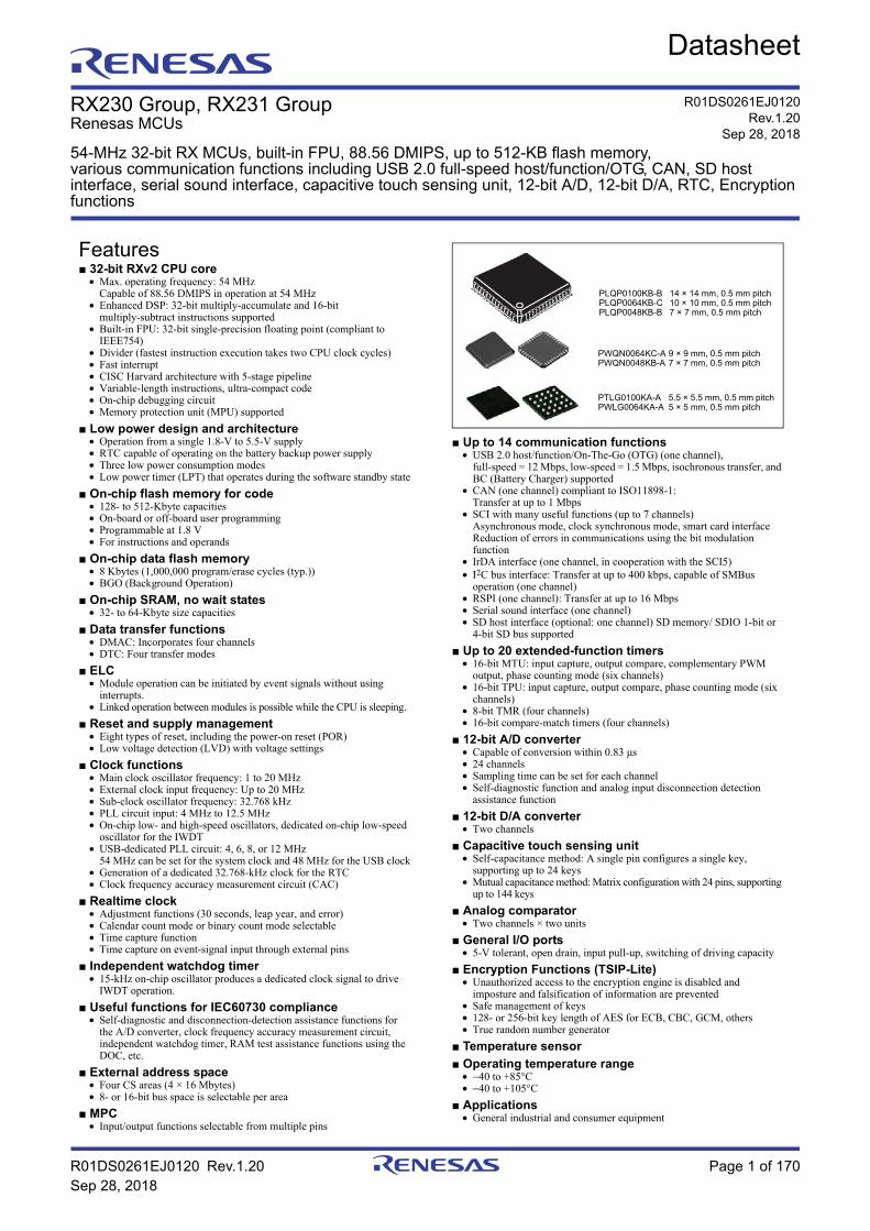
Datasheet R01DS0261EJ0120 Rev.1.20 Page 1 of 170 Sep 28, 2018 RX230 Group, RX231 Group Renesas MCUs Features ■ 32-bit RXv2 CPU core • Max. operating frequency: 54 MHz Capable of 88.56 DMIPS in operation at 54 MHz • Enhanced DSP: 32-bit multiply-accumulate and 16-bit multiply-subtract instructions supported • Built-in FPU: 32-bit single-precision floating point (compliant to IEEE754) • Divider (fastest instruction execution takes two CPU clock cycles) • Fast interrupt • CISC Harvard architecture with 5-stage pipeline • Variable-length instructions, ultra-compact code • On-chip debugging circuit • Memory protection unit (MPU) supported ■ Low power design and architecture • Operation from a single 1.8-V to 5.5-V supply • RTC capable of operating on the battery backup power supply • Three low power consumption modes • Low power timer (LPT) that operates during the software standby state ■ On-chip flash memory for code • 128- to 512-Kbyte capacities • On-board or off-board user programming • Programmable at 1.8 V • For instructions and operands ■ On-chip data flash memory • 8 Kbytes (1,000,000 program/erase cycles (typ.)) • BGO (Background Operation) ■ On-chip SRAM, no wait states • 32- to 64-Kbyte size capacities ■ Data transfer functions • DMAC: Incorporates four channels • DTC: Four transfer modes ■ ELC • Module operation can be initiated by event signals without using interrupts. • Linked operation between modules is possible while the CPU is sleeping. ■ Reset and supply management • Eight types of reset, including the power-on reset (POR) • Low voltage detection (LVD) with voltage settings ■ Clock functions • Main clock oscillator frequency: 1 to 20 MHz • External clock input frequency: Up to 20 MHz • Sub-clock oscillator frequency: 32.768 kHz • PLL circuit input: 4 MHz to 12.5 MHz • On-chip low- and high-speed oscillators, dedicated on-chip low-speed oscillator for the IWDT • USB-dedicated PLL circuit: 4, 6, 8, or 12 MHz 54 MHz can be set for the system clock and 48 MHz for the USB clock • Generation of a dedicated 32.768-kHz clock for the RTC • Clock frequency accuracy measurement circuit (CAC) ■ Realtime clock • Adjustment functions (30 seconds, leap year, and error) • Calendar count mode or binary count mode selectable • Time capture function • Time capture on event-signal input through external pins ■ Independent watchdog timer • 15-kHz on-chip oscillator produces a dedicated clock signal to drive IWDT operation. ■ Useful functions for IEC60730 compliance • Self-diagnostic and disconnection-detection assistance functions for the A/D converter, clock frequency accuracy measurement circuit, independent watchdog timer, RAM test assistance functions using the DOC, etc. ■ External address space • Four CS areas (4 × 16 Mbytes) • 8- or 16-bit bus space is selectable per area ■ MPC • Input/output functions selectable from multiple pins ■ Up to 14 communication functions • USB 2.0 host/function/On-The-Go (OTG) (one channel), full-speed = 12 Mbps, low-speed = 1.5 Mbps, isochronous transfer, and BC (Battery Charger) supported • CAN (one channel) compliant to ISO11898-1: Transfer at up to 1 Mbps • SCI with many useful functions (up to 7 channels) Asynchronous mode, clock synchronous mode, smart card interface Reduction of errors in communications using the bit modulation function • IrDA interface (one channel, in cooperation with the SCI5) • I 2 C bus interface: Transfer at up to 400 kbps, capable of SMBus operation (one channel) • RSPI (one channel): Transfer at up to 16 Mbps • Serial sound interface (one channel) • SD host interface (optional: one channel) SD memory/ SDIO 1-bit or 4-bit SD bus supported ■ Up to 20 extended-function timers • 16-bit MTU: input capture, output compare, complementary PWM output, phase counting mode (six channels) • 16-bit TPU: input capture, output compare, phase counting mode (six channels) • 8-bit TMR (four channels) • 16-bit compare-match timers (four channels) ■ 12-bit A/D converter • Capable of conversion within 0.83 μs • 24 channels • Sampling time can be set for each channel • Self-diagnostic function and analog input disconnection detection assistance function ■ 12-bit D/A converter • Two channels ■ Capacitive touch sensing unit • Self-capacitance method: A single pin configures a single key, supporting up to 24 keys • Mutual capacitance method: Matrix configuration with 24 pins, supporting up to 144 keys ■ Analog comparator • Two channels × two units ■ General I/O ports • 5-V tolerant, open drain, input pull-up, switching of driving capacity ■ Encryption Functions (TSIP-Lite) • Unauthorized access to the encryption engine is disabled and imposture and falsification of information are prevented • Safe management of keys • 128- or 256-bit key length of AES for ECB, CBC, GCM, others • True random number generator ■ Temperature sensor ■ Operating temperature range •−40 to +85°C •−40 to +105°C ■ Applications • General industrial and consumer equipment PLQP0100KB-B 14 × 14 mm, 0.5 mm pitch PLQP0064KB-C 10 × 10 mm, 0.5 mm pitch PLQP0048KB-B 7 × 7 mm, 0.5 mm pitch PWQN0064KC-A 9 × 9 mm, 0.5 mm pitch PWQN0048KB-A 7 × 7 mm, 0.5 mm pitch PTLG0100KA-A 5.5 × 5.5 mm, 0.5 mm pitch PWLG0064KA-A 5 × 5 mm, 0.5 mm pitch 54-MHz 32-bit RX MCUs, built-in FPU, 88.56 DMIPS, up to 512-KB flash memory, various communication functions including USB 2.0 full-speed host/function/OTG, CAN, SD host interface, serial sound interface, capacitive touch sensing unit, 12-bit A/D, 12-bit D/A, RTC, Encryption functions R01DS0261EJ0120 Rev.1.20 Sep 28, 2018

Welcome message from author
This document is posted to help you gain knowledge. Please leave a comment to let me know what you think about it! Share it to your friends and learn new things together.
Transcript
Datasheet
R01DS0261EJ0120 Rev.1.20 Page 1 of 170Sep 28, 2018
RX230 Group, RX231 GroupRenesas MCUs
Features■ 32-bit RXv2 CPU core
• Max. operating frequency: 54 MHzCapable of 88.56 DMIPS in operation at 54 MHz
• Enhanced DSP: 32-bit multiply-accumulate and 16-bit multiply-subtract instructions supported
• Built-in FPU: 32-bit single-precision floating point (compliant to IEEE754)
• Divider (fastest instruction execution takes two CPU clock cycles)• Fast interrupt• CISC Harvard architecture with 5-stage pipeline• Variable-length instructions, ultra-compact code• On-chip debugging circuit• Memory protection unit (MPU) supported
■ Low power design and architecture• Operation from a single 1.8-V to 5.5-V supply• RTC capable of operating on the battery backup power supply• Three low power consumption modes• Low power timer (LPT) that operates during the software standby state
■ On-chip flash memory for code• 128- to 512-Kbyte capacities• On-board or off-board user programming• Programmable at 1.8 V• For instructions and operands
■ On-chip data flash memory• 8 Kbytes (1,000,000 program/erase cycles (typ.))• BGO (Background Operation)
■ On-chip SRAM, no wait states• 32- to 64-Kbyte size capacities
■ Data transfer functions• DMAC: Incorporates four channels • DTC: Four transfer modes
■ ELC• Module operation can be initiated by event signals without using
interrupts.• Linked operation between modules is possible while the CPU is sleeping.
■ Reset and supply management• Eight types of reset, including the power-on reset (POR)• Low voltage detection (LVD) with voltage settings
■ Clock functions• Main clock oscillator frequency: 1 to 20 MHz• External clock input frequency: Up to 20 MHz• Sub-clock oscillator frequency: 32.768 kHz• PLL circuit input: 4 MHz to 12.5 MHz• On-chip low- and high-speed oscillators, dedicated on-chip low-speed
oscillator for the IWDT• USB-dedicated PLL circuit: 4, 6, 8, or 12 MHz
54 MHz can be set for the system clock and 48 MHz for the USB clock• Generation of a dedicated 32.768-kHz clock for the RTC• Clock frequency accuracy measurement circuit (CAC)
■ Realtime clock• Adjustment functions (30 seconds, leap year, and error)• Calendar count mode or binary count mode selectable• Time capture function• Time capture on event-signal input through external pins
■ Independent watchdog timer• 15-kHz on-chip oscillator produces a dedicated clock signal to drive
IWDT operation.■ Useful functions for IEC60730 compliance
• Self-diagnostic and disconnection-detection assistance functions for the A/D converter, clock frequency accuracy measurement circuit, independent watchdog timer, RAM test assistance functions using the DOC, etc.
■ External address space• Four CS areas (4 × 16 Mbytes)• 8- or 16-bit bus space is selectable per area
■ MPC• Input/output functions selectable from multiple pins
■ Up to 14 communication functions• USB 2.0 host/function/On-The-Go (OTG) (one channel),
full-speed = 12 Mbps, low-speed = 1.5 Mbps, isochronous transfer, and BC (Battery Charger) supported
• CAN (one channel) compliant to ISO11898-1: Transfer at up to 1 Mbps
• SCI with many useful functions (up to 7 channels)Asynchronous mode, clock synchronous mode, smart card interfaceReduction of errors in communications using the bit modulation function
• IrDA interface (one channel, in cooperation with the SCI5)• I2C bus interface: Transfer at up to 400 kbps, capable of SMBus
operation (one channel)• RSPI (one channel): Transfer at up to 16 Mbps• Serial sound interface (one channel)• SD host interface (optional: one channel) SD memory/ SDIO 1-bit or
4-bit SD bus supported■ Up to 20 extended-function timers
• 16-bit MTU: input capture, output compare, complementary PWM output, phase counting mode (six channels)
• 16-bit TPU: input capture, output compare, phase counting mode (six channels)
• 8-bit TMR (four channels) • 16-bit compare-match timers (four channels)
■ 12-bit A/D converter• Capable of conversion within 0.83 μs• 24 channels• Sampling time can be set for each channel• Self-diagnostic function and analog input disconnection detection
assistance function■ 12-bit D/A converter
• Two channels■ Capacitive touch sensing unit
• Self-capacitance method: A single pin configures a single key, supporting up to 24 keys
• Mutual capacitance method: Matrix configuration with 24 pins, supporting up to 144 keys
■ Analog comparator• Two channels × two units
■ General I/O ports• 5-V tolerant, open drain, input pull-up, switching of driving capacity
■ Encryption Functions (TSIP-Lite)• Unauthorized access to the encryption engine is disabled and
imposture and falsification of information are prevented• Safe management of keys • 128- or 256-bit key length of AES for ECB, CBC, GCM, others• True random number generator
■ Temperature sensor■ Operating temperature range
• −40 to +85°C• −40 to +105°C
■ Applications• General industrial and consumer equipment
PLQP0100KB-B 14 × 14 mm, 0.5 mm pitchPLQP0064KB-C 10 × 10 mm, 0.5 mm pitchPLQP0048KB-B 7 × 7 mm, 0.5 mm pitch
PWQN0064KC-A 9 × 9 mm, 0.5 mm pitchPWQN0048KB-A 7 × 7 mm, 0.5 mm pitch
PTLG0100KA-A 5.5 × 5.5 mm, 0.5 mm pitchPWLG0064KA-A 5 × 5 mm, 0.5 mm pitch
54-MHz 32-bit RX MCUs, built-in FPU, 88.56 DMIPS, up to 512-KB flash memory, various communication functions including USB 2.0 full-speed host/function/OTG, CAN, SD host interface, serial sound interface, capacitive touch sensing unit, 12-bit A/D, 12-bit D/A, RTC, Encryption functions
R01DS0261EJ0120Rev.1.20
Sep 28, 2018
R01DS0261EJ0120 Rev.1.20 Page 2 of 170Sep 28, 2018
RX230 Group, RX231 Group 1. Overview
1. Overview
1.1 Outline of SpecificationsTable 1.1 lists the specifications, and Table 1.2 gives a comparison of the functions of the products in different packages.Table 1.1 is for products with the greatest number of functions, so the number of peripheral modules and channels will differ in accordance with the package type. For details, see Table 1.2, Comparison of Functions for Different Packages.
Table 1.1 Outline of Specifications (1/4)Classification Module/Function Description
CPU CPU • Maximum operating frequency: 54 MHz• 32-bit RX CPU (RX v2)• Minimum instruction execution time: One instruction per clock cycle• Address space: 4-Gbyte linear• Register set
General purpose: Sixteen 32-bit registersControl: Ten 32-bit registersAccumulator: Two 72-bit registers
• Basic instructions: 75 (variable-length instruction format)• Floating-point instructions: 11• DSP instructions: 23• Addressing modes: 10• Data arrangement
Instructions: Little endianData: Selectable as little endian or big endian
• On-chip 32-bit multiplier: 32-bit × 32-bit → 64-bit• On-chip divider: 32-bit ÷ 32-bit → 32 bits• Barrel shifter: 32 bits• Memory protection unit (MPU)
FPU • Single precision (32-bit) floating point• Data types and floating-point exceptions in conformance with the IEEE754 standard
Memory ROM • Capacity: 128/256/384/512 Kbytes• Up to 32 MHz: No-wait memory access
32 to 54 MHz: Wait state required. No wait state if the instruction is served by a ROM accelerator hit.• Programming/erasing method:
Serial programming (asynchronous serial communication/USB communication), self-programming
RAM • Capacity: 32/64 Kbytes• 54 MHz, no-wait memory access
E2 DataFlash • Capacity: 8 Kbytes• Number of erase/write cycles: 1,000,000 (typ)
MCU operating mode Single-chip mode, on-chip ROM enabled expansion mode, and on-chip ROM disabled expansion mode (software switching)
Clock Clock generation circuit • Main clock oscillator, sub-clock oscillator, low-speed on-chip oscillator, high-speed on-chip oscillator, PLL frequency synthesizer, USB-dedicated PLL frequency synthesizer, and IWDT-dedicated on-chip oscillator
• Oscillation stop detection: Available• Clock frequency accuracy measurement circuit (CAC)• Independent settings for the system clock (ICLK), peripheral module clock (PCLK), external bus clock
(BCLK), and FlashIF clock (FCLK)The CPU and system sections such as other bus masters run in synchronization with the system clock (ICLK): 54 MHz (at max.)MTU2a runs in synchronization with the PCLKA: 54 MHz (at max.)The ADCLK for the S12AD runs in synchronization with the PCLKD: 54 MHz (at max.)Peripheral modules other than MTU2a and S12ADE run in synchronization with the PCLKB: 32 MHz (at max.)Devices connected to external buses run in synchronization with the BCLK: 32 MHz (at max.)The flash peripheral circuit runs in synchronization with the FCLK: 32 MHz (at max.)
Resets RES# pin reset, power-on reset, voltage monitoring reset, watchdog timer reset, independent watchdog timer reset, and software reset
Voltage detection Voltage detection circuit (LVDAb)
• When the voltage on VCC falls below the voltage detection level, an internal reset or internal interrupt is generated.Voltage detection circuit 0 is capable of selecting the detection voltage from 4 levelsVoltage detection circuit 1 is capable of selecting the detection voltage from 14 levelsVoltage detection circuit 2 is capable of selecting the detection voltage from 4 levels
R01DS0261EJ0120 Rev.1.20 Page 3 of 170Sep 28, 2018
RX230 Group, RX231 Group 1. Overview
Low power consumption
Low power consumption functions
• Module stop function• Three low power consumption modes
Sleep mode, deep sleep mode, and software standby mode• Low power timer that operates during the software standby state
Function for lower operating power consumption
• Operating power control modesHigh-speed operating mode, middle-speed operating mode, and low-speed operating mode
Interrupt Interrupt controller (ICUb) • Interrupt vectors: 167• External interrupts: 9 (NMI, IRQ0 to IRQ7 pins)• Non-maskable interrupts: 7 (NMI pin, oscillation stop detection interrupt, voltage monitoring 1
interrupt, voltage monitoring 2 interrupt, WDT interrupt, IWDT interrupt, and VBATT power monitoring interrupt)
• 16 levels specifiable for the order of priority
External bus extension • The external address space can be divided into four areas (CS0 to CS3), each with independent control of access settings.Capacity of each area: 16 Mbytes (CS0 to CS3)A chip-select signal (CS0# to CS3#) can be output for each area.Each area is specifiable as an 8-bit or 16-bit bus spaceThe data arrangement in each area is selectable as little or big endian (only for data).Bus format: Separate bus, multiplex bus
• Wait control• Write buffer facility
DMA DMA controller (DMACA) • 4 channels• Three transfer modes: Normal transfer, repeat transfer, and block transfer• Activation sources: Software trigger, external interrupts, and interrupt requests from peripheral
functions
Data transfer controller (DTCa)
• Transfer modes: Normal transfer, repeat transfer, and block transfer• Activation sources: Interrupts• Chain transfer function
I/O ports General I/O ports 100-pin/64-pin/48-pinI/O: 79/43/30 (RX231 Group), 83/47/34 (RX230 Group)• Input: 1/1/1Pull-up resistors: 79/43/30(RX231 Group), 83/47/34 (RX230 Group)• Open-drain outputs: 58/34/26• 5-V tolerance: 8/5/5
Event link controller (ELC) • Event signals of 61 types can be directly connected to the module• Operations of timer modules are selectable at event input• Capable of event link operation for port B and port E
Multi-function pin controller (MPC) Capable of selecting the input/output function from multiple pins
Timers 16-bit timer pulse unit (TPUa)
• (16 bits × 6 channels) × 1 unit• Maximum of 16 pulse-input/output possible• Select from among seven or eight counter-input clock signals for each channel• Supports the input capture/output compare function• Output of PWM waveforms in up to 15 phases in PWM mode• Support for buffered operation, phase-counting mode (two-phase encoder input) and cascade
connected operation (32 bits × 2 channels) depending on the channel.• Capable of generating conversion start triggers for the A/D converters• Signals from the input capture pins are input via a digital filter• Clock frequency measuring method
Multi-function timer pulse unit 2 (MTU2a)
• (16 bits × 6 channels) × 1 unit• Up to 16 pulse-input/output lines and three pulse-input lines are available based on the six 16-bit
timer channels• Select from among eight or seven counter-input clock signals for each channel (PCLK/1, PCLK/4,
PCLK/16, PCLK/64, PCLK/256, PCLK/1024, MTCLKA, MTCLKB, MTCLKC, MTCLKD) other than channel 5, for which only four signals are available.
• Input capture function• 21 output compare/input capture registers• Pulse output mode• Complementary PWM output mode• Reset synchronous PWM mode• Phase-counting mode• Capable of generating conversion start triggers for the A/D converter
Port output enable 2 (POE2a)
Controls the high-impedance state of the MTU’s waveform output pins
Compare match timer (CMT)
• (16 bits × 2 channels) × 2 units• Select from among four clock signals (PCLK/8, PCLK/32, PCLK/128, PCLK/512)
Watchdog timer (WDTA) • 14 bits x 1 channel• Select from among six counter-input clock signals (PCLK/4, PCLK/64, PCLK/128, PCLK/512, PCLK/
2048, PCLK/8192)
Table 1.1 Outline of Specifications (2/4)Classification Module/Function Description

R01DS0261EJ0120 Rev.1.20 Page 4 of 170Sep 28, 2018
RX230 Group, RX231 Group 1. Overview
Timers Independent watchdog timer (IWDTa)
• 14 bits × 1 channel• Count clock: Dedicated low-speed on-chip oscillator for the IWDT
Frequency divided by 1, 16, 32, 64, 128, or 256
Realtime clock (RTCe) • Clock source: Sub-clock• Time/calendar• Interrupts: Alarm interrupt, periodic interrupt, and carry interrupt• Time-capture facility for three values
Low power timer (LPT) • 16 bits × 1 channel• Clock source: Sub-clock, Dedicated low-speed on-chip oscillator for the IWDT
Frequency divided by 2, 4, 8, 16, or 32
8-bit timer (TMR) • (8 bits × 2 channels) × 2 units• Seven internal clocks (PCLK/1, PCLK/2, PCLK/8, PCLK/32, PCLK/64, PCLK/1024, and PCLK/8192)
and an external clock can be selected• Pulse output and PWM output with any duty cycle are available• Two channels can be cascaded and used as a 16-bit timer
Communication functions
Serial communications interfaces (SCIg, SCIh)
• 7 channels (channel 0, 1, 5, 6, 8, 9: SCIg, channel 12: SCIh)• SCIg
Serial communications modes: Asynchronous, clock synchronous, and smart-card interfaceMulti-processor functionOn-chip baud rate generator allows selection of the desired bit rateChoice of LSB-first or MSB-first transferAverage transfer rate clock can be input from TMR timers for SCI5, SCI6, and SCI12Start-bit detection: Level or edge detection is selectable.Simple I2CSimple SPI9-bit transfer modeBit rate modulationEvent linking by the ELC (only on channel 5)
• SCIh (The following functions are added to SCIg)Supports the serial communications protocol, which contains the start frame and information frameSupports the LIN format
IrDA interface (IRDA) • 1 channel (SCI5 used)• Supports encoding/decoding of waveforms conforming to IrDA standard 1.0
I2C bus interface (RIICa) • 1 channel• Communications formats: I2C bus format/SMBus format• Master mode or slave mode selectable• Supports fast mode
Serial peripheral interface (RSPIa)
• 1 channel• Transfer facility
Using the MOSI (master out, slave in), MISO (master in, slave out), SSL (slave select), and RSPCK (RSPI clock) enables serial transfer through SPI operation (four lines) or clock-synchronous operation (three lines)
• Capable of handling serial transfer as a master or slave• Data formats• Choice of LSB-first or MSB-first transfer
The number of bits in each transfer can be changed to 8, 9, 10, 11, 12, 13, 14, 15, 16, 20, 24, or 32 bits.128-bit buffers for transmission and receptionUp to four frames can be transmitted or received in a single transfer operation (with each frame having up to 32 bits)
• Double buffers for both transmission and reception
USB 2.0 host/function module (USBd)
• USB Device Controller (UDC) and transceiver for USB 2.0 are incorporated.• Host/function module: 1 port• Compliant with USB version 2.0• Transfer speed: Full-speed (12 Mbps), low-speed (1.5 Mbps)• OTG (ON-The-Go) is supported.• Isochronous transfer is supported.• BC1.2 (Battery Charging Specification Revision 1.2) is supported.• Internal power supply for USB (allows operation without external power input to the VCC_USB pin
when VCC = 4.0 to 5.5V)
CAN module (RSCAN) • 1 channel• Compliance with the ISO11898-1 specification (standard frame and extended frame)• 16 Message boxes
Table 1.1 Outline of Specifications (3/4)Classification Module/Function Description
R01DS0261EJ0120 Rev.1.20 Page 5 of 170Sep 28, 2018
RX230 Group, RX231 Group 1. Overview
Communication functions
Serial Sound Interface (SSI) • 1 channel• Capable of duplex communications• Various serial audio formats supported• Master/slave function supported• Programmable word clock or bit clock generation function• 8/16/18/20/22/24/32-bit data formats supported• On-chip 8-stage FIFO for transmission/reception• Supports WS continue mode in which the SSIWS signal is not stopped.
SD Host Interface (SDHIa) • 1 channel• Transfer speed : Default speed mode (8MB/s)• SD memory card interface (1 bit / 4bits SD bus)• MMC, eMMC Backward-compatible are supported.• SD Specifications
Part 1: Compliant with Physical Layer Specification Ver.3.01 (Not support DDR)Part E1: SDIO Specification Ver. 3.00
• Error check function: CRC7 (command), CRC16 (data)• Interrupt Source: Card access interrupt, SDIO access interrupt, Card detection interrupt, SD buffer
access interrupt• DMA transfer sources: SD_BUF write, SD_BUF read• Card detection, Write protection
Encryption functions
Trusted Secure IP (TSIP-Lite)
• Access management circuit • Encryption engine
128- or 256-bit key sizes of AESBlock cipher mode of operation: GCM, ECB, CBC, CMAC, XTS, CTR, GCTR
• Hash function• True random number generator• Prevention from illicit copying of a key
12-bit A/D converter (S12ADE) • 12 bits (24 channels × 1 unit)• 12-bit resolution• Minimum conversion time: 0.83 µs per channel when the ADCLK is operating at 54 MHz• Operating modes
Scan mode (single scan mode, continuous scan mode, and group scan mode)Group A priority control (only for group scan mode)
• Sampling variableSampling time can be set up for each channel.
• Self-diagnostic function• Double trigger mode (A/D conversion data duplicated)• Detection of analog input disconnection• A/D conversion start conditions
A software trigger, a trigger from a timer (MTU, TPU), an external trigger signal, or ELC• Event linking by the ELC
Temperature sensor (TEMPSA) • 1 channel• The voltage output from the temperature sensor is converted into a digital value by the 12-bit A/D
converter.
12-bit D/A converter (R12DAA) • 2 channels• 12-bit resolution• Output voltage: 0.4 to AVCC0-0.5V
CRC calculator (CRC) • CRC code generation for arbitrary amounts of data in 8-bit units• Select any of three generating polynomials:
X8 + X2 + X + 1, X16 + X15 + X2 + 1, or X16 + X12 + X5 + 1• Generation of CRC codes for use with LSB-first or MSB-first communications is selectable.
Comparator B (CMPBa) • 2 channels × 2 units• Function to compare the reference voltage and the analog input voltage• Window comparator operation or standard comparator operation is selectable
Capacitive touch sensing unit (CTSU) Detection pin: 24 channels
Data operation circuit (DOC) Comparison, addition, and subtraction of 16-bit data
Power supply voltages/Operating frequencies VCC = 1.8 to 2.4 V: 8 MHz, VCC = 2.4 to 2.7 V: 16 MHz, VCC = 2.7 to 5.5 V: 54 MHz
Operating temperature range D version: −40 to +85°C, G version: −40 to +105°C
Packages 100-pin TFLGA (PTLG0100KA-A) 5.5 × 5.5 mm, 0.5 mm pitch100-pin LFQFP (PLQP0100KB-B) 14 × 14 mm, 0.5 mm pitch64-pin WFLGA (PWLG0064KA-A) 5 × 5 mm, 0.5 mm pitch64-pin HWQFN (PWQN0064KC-A) 9 × 9 mm, 0.5 mm pitch64-pin LFQFP (PLQP0064KB-C) 10 × 10 mm, 0.5 mm pitch48-pin HWQFN (PWQN0048KB-A) 7 × 7 mm, 0.5 mm pitch48-pin LFQFP (PLQP0048KB-B) 7 × 7 mm, 0.5 mm pitch
Debugging interfaces FINE interface
Table 1.1 Outline of Specifications (4/4)Classification Module/Function Description
R01DS0261EJ0120 Rev.1.20 Page 6 of 170Sep 28, 2018
RX230 Group, RX231 Group 1. Overview
Note 1. Only for chip version B
Table 1.2 Comparison of Functions for Different Packages
Module/Functions
RX230 Group RX231 Group
100 Pins 64 Pins 48 Pins 100 Pins 64 Pins 48 Pins
External bus External bus 16 bit Not supported 16 bit Not supported
Interrupts External interrupts NMI, IRQ0 to IRQ7
NMI, IRQ0, IRQ1, IRQ4
to IRQ7
NMI, IRQ0, IRQ1, IRQ4
to IRQ7
NMI, IRQ0 to IRQ7
NMI, IRQ0, IRQ1, IRQ4
to IRQ7
NMI, IRQ0, IRQ1, IRQ4
to IRQ7
DMA DMA controller 4 channels (DMAC0 to DMAC3) 4 channels (DMAC0 to DMAC3)
Data transfer controller Available Available
Timers 16-bit timer pulse unit 6 channels (TPU0 to TPU5) 6 channels (TPU0 to TPU5)
Multi-function timer pulse unit 2 6 channels (MTU0 to MTU5) 6 channels (MTU0 to MTU5)
Port output enable 2 POE0# to POE3#, POE8# POE0# to POE3#, POE8#
8-bit timer 2 channels× 2 units 2 channels× 2 units
Compare match timer 2 channels× 2 units 2 channels× 2 units
Low power timer 1 channel 1 channel
Realtime clock Available Not supported
Available Not supported
Watchdog timer Available Available
Independent watchdog timer Available Available
Communicationfunctions
Serial communications interfaces (SCIg)
6 channels (SCI0, 1, 5,
6, 8, 9)
5 channels (SCI1, 5, 6,
8, 9)
4 channels (SCI1, 5, 6,
8)
6 channels (SCI0, 1, 5,
6, 8, 9)
5 channels (SCI1, 5, 6,
8, 9)
4 channels (SCI1, 5, 6,
8)
IrDA interface 1 channel (SCI5) 1 channel (SCI5)
Serial communications interfaces (SCIh)
1 channel (SCI12) 1 channel (SCI12)
I2C bus interface 1 channel 1 channel
CAN module Not supported 1 channel*1
Serial peripheral interface 1 channel 1 channel
USB 2.0 host/function module Not supported 1 channel
Serial sound interface 1 channel 1 channel
SD Host Interface Not supported 1 channel*1 Not supported
Capacitive touch sensing unit 24 channels 10 channels 6 channels 24 channels 10 channels 6 channels
12-bit A/D converter(including high-precision channels)
24 channels (8
channels)
12 channels (6
channels)
8 channels (4
channels)
24 channels (8
channels)
12 channels (6
channels)
8 channels (4
channels)
Temperature sensor Available Available
D/A converter 2 channels Not supported
2 channels Not supported
CRC calculator Available Available
Event link controller Available Available
Comparator B 4 channels 4 channels
Packages 100-pin TFLGA100-pin LFQFP
64-pin WFLGA64-pin
HWQFN64-pin LFQFP
48-pin HWQFN48-pin LFQFP
100-pin TFLGA100-pin LFQFP
64-pin WFLGA64-pin
HWQFN64-pin LFQFP
48-pin HWQFN48-pin LFQFP
R01DS0261EJ0120 Rev.1.20 Page 7 of 170Sep 28, 2018
RX230 Group, RX231 Group 1. Overview
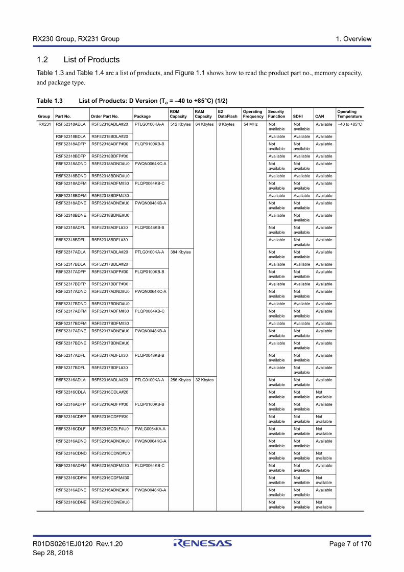
1.2 List of ProductsTable 1.3 and Table 1.4 are a list of products, and Figure 1.1 shows how to read the product part no., memory capacity, and package type.
Table 1.3 List of Products: D Version (Ta = –40 to +85°C) (1/2)
Group Part No. Order Part No. PackageROM Capacity
RAM Capacity
E2 DataFlash
OperatingFrequency
Security Function SDHI CAN
OperatingTemperature
RX231 R5F52318ADLA R5F52318ADLA#20 PTLG0100KA-A 512 Kbytes 64 Kbytes 8 Kbytes 54 MHz Not available
Not available
Available −40 to +85°C
R5F52318BDLA R5F52318BDLA#20 Available Available Available
R5F52318ADFP R5F52318ADFP#30 PLQP0100KB-B Not available
Not available
Available
R5F52318BDFP R5F52318BDFP#30 Available Available Available
R5F52318ADND R5F52318ADND#U0 PWQN0064KC-A Not available
Not available
Available
R5F52318BDND R5F52318BDND#U0 Available Available Available
R5F52318ADFM R5F52318ADFM#30 PLQP0064KB-C Not available
Not available
Available
R5F52318BDFM R5F52318BDFM#30 Available Available Available
R5F52318ADNE R5F52318ADNE#U0 PWQN0048KB-A Not available
Not available
Available
R5F52318BDNE R5F52318BDNE#U0 Available Not available
Available
R5F52318ADFL R5F52318ADFL#30 PLQP0048KB-B Not available
Not available
Available
R5F52318BDFL R5F52318BDFL#30 Available Not available
Available
R5F52317ADLA R5F52317ADLA#20 PTLG0100KA-A 384 Kbytes Not available
Not available
Available
R5F52317BDLA R5F52317BDLA#20 Available Available Available
R5F52317ADFP R5F52317ADFP#30 PLQP0100KB-B Not available
Not available
Available
R5F52317BDFP R5F52317BDFP#30 Available Available Available
R5F52317ADND R5F52317ADND#U0 PWQN0064KC-A Not available
Not available
Available
R5F52317BDND R5F52317BDND#U0 Available Available Available
R5F52317ADFM R5F52317ADFM#30 PLQP0064KB-C Not available
Not available
Available
R5F52317BDFM R5F52317BDFM#30 Available Available Available
R5F52317ADNE R5F52317ADNE#U0 PWQN0048KB-A Not available
Not available
Available
R5F52317BDNE R5F52317BDNE#U0 Available Not available
Available
R5F52317ADFL R5F52317ADFL#30 PLQP0048KB-B Not available
Not available
Available
R5F52317BDFL R5F52317BDFL#30 Available Not available
Available
R5F52316ADLA R5F52316ADLA#20 PTLG0100KA-A 256 Kbytes 32 Kbytes Not available
Not available
Available
R5F52316CDLA R5F52316CDLA#20 Not available
Not available
Not available
R5F52316ADFP R5F52316ADFP#30 PLQP0100KB-B Not available
Not available
Available
R5F52316CDFP R5F52316CDFP#30 Not available
Not available
Not available
R5F52316CDLF R5F52316CDLF#U0 PWLG0064KA-A Not available
Not available
Not available
R5F52316ADND R5F52316ADND#U0 PWQN0064KC-A Not available
Not available
Available
R5F52316CDND R5F52316CDND#U0 Not available
Not available
Not available
R5F52316ADFM R5F52316ADFM#30 PLQP0064KB-C Not available
Not available
Available
R5F52316CDFM R5F52316CDFM#30 Not available
Not available
Not available
R5F52316ADNE R5F52316ADNE#U0 PWQN0048KB-A Not available
Not available
Available
R5F52316CDNE R5F52316CDNE#U0 Not available
Not available
Not available
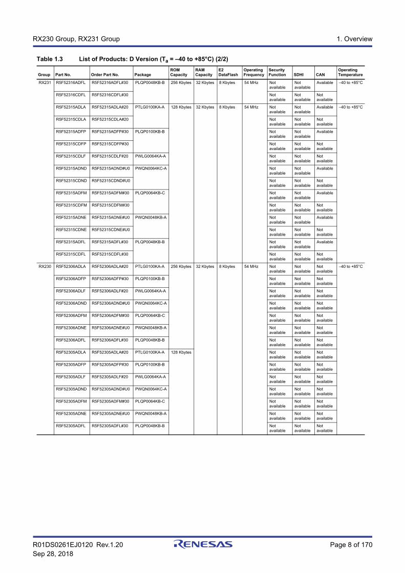
R01DS0261EJ0120 Rev.1.20 Page 8 of 170Sep 28, 2018
RX230 Group, RX231 Group 1. Overview
RX231 R5F52316ADFL R5F52316ADFL#30 PLQP0048KB-B 256 Kbytes 32 Kbytes 8 Kbytes 54 MHz Not available
Not available
Available −40 to +85°C
R5F52316CDFL R5F52316CDFL#30 Not available
Not available
Not available
R5F52315ADLA R5F52315ADLA#20 PTLG0100KA-A 128 Kbytes 32 Kbytes 8 Kbytes 54 MHz Not available
Not available
Available −40 to +85°C
R5F52315CDLA R5F52315CDLA#20 Not available
Not available
Not available
R5F52315ADFP R5F52315ADFP#30 PLQP0100KB-B Not available
Not available
Available
R5F52315CDFP R5F52315CDFP#30 Not available
Not available
Not available
R5F52315CDLF R5F52315CDLF#20 PWLG0064KA-A Not available
Not available
Not available
R5F52315ADND R5F52315ADND#U0 PWQN0064KC-A Not available
Not available
Available
R5F52315CDND R5F52315CDND#U0 Not available
Not available
Not available
R5F52315ADFM R5F52315ADFM#30 PLQP0064KB-C Not available
Not available
Available
R5F52315CDFM R5F52315CDFM#30 Not available
Not available
Not available
R5F52315ADNE R5F52315ADNE#U0 PWQN0048KB-A Not available
Not available
Available
R5F52315CDNE R5F52315CDNE#U0 Not available
Not available
Not available
R5F52315ADFL R5F52315ADFL#30 PLQP0048KB-B Not available
Not available
Available
R5F52315CDFL R5F52315CDFL#30 Not available
Not available
Not available
RX230 R5F52306ADLA R5F52306ADLA#20 PTLG0100KA-A 256 Kbytes 32 Kbytes 8 Kbytes 54 MHz Not available
Not available
Not available
−40 to +85°C
R5F52306ADFP R5F52306ADFP#30 PLQP0100KB-B Not available
Not available
Not available
R5F52306ADLF R5F52306ADLF#20 PWLG0064KA-A Not available
Not available
Not available
R5F52306ADND R5F52306ADND#U0 PWQN0064KC-A Not available
Not available
Not available
R5F52306ADFM R5F52306ADFM#30 PLQP0064KB-C Not available
Not available
Not available
R5F52306ADNE R5F52306ADNE#U0 PWQN0048KB-A Not available
Not available
Not available
R5F52306ADFL R5F52306ADFL#30 PLQP0048KB-B Not available
Not available
Not available
R5F52305ADLA R5F52305ADLA#20 PTLG0100KA-A 128 Kbytes Not available
Not available
Not available
R5F52305ADFP R5F52305ADFP#30 PLQP0100KB-B Not available
Not available
Not available
R5F52305ADLF R5F52305ADLF#20 PWLG0064KA-A Not available
Not available
Not available
R5F52305ADND R5F52305ADND#U0 PWQN0064KC-A Not available
Not available
Not available
R5F52305ADFM R5F52305ADFM#30 PLQP0064KB-C Not available
Not available
Not available
R5F52305ADNE R5F52305ADNE#U0 PWQN0048KB-A Not available
Not available
Not available
R5F52305ADFL R5F52305ADFL#30 PLQP0048KB-B Not available
Not available
Not available
Table 1.3 List of Products: D Version (Ta = –40 to +85°C) (2/2)
Group Part No. Order Part No. PackageROM Capacity
RAM Capacity
E2 DataFlash
OperatingFrequency
Security Function SDHI CAN
OperatingTemperature

R01DS0261EJ0120 Rev.1.20 Page 9 of 170Sep 28, 2018
RX230 Group, RX231 Group 1. Overview
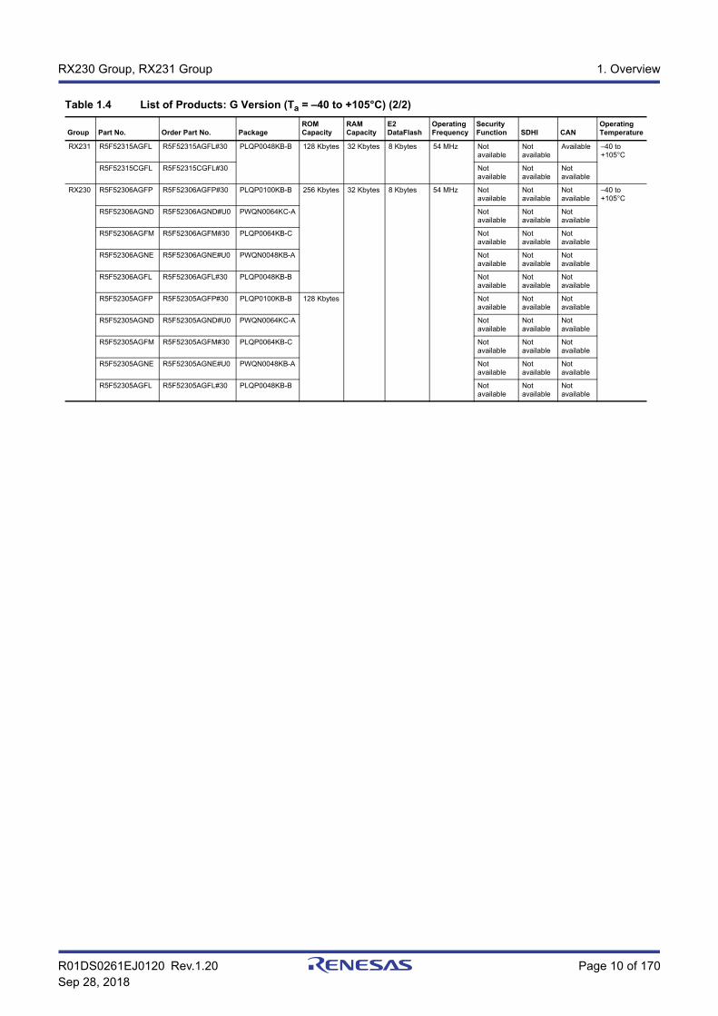
Table 1.4 List of Products: G Version (Ta = –40 to +105°C) (1/2)
Group Part No. Order Part No. PackageROM Capacity
RAM Capacity
E2 DataFlash
OperatingFrequency
Security Function SDHI CAN
OperatingTemperature
RX231 R5F52318AGFP R5F52318AGFP#30 PLQP0100KB-B 512 Kbytes 64 Kbytes 8 Kbytes 54 MHz Not available
Not available
Available −40 to +105°C
R5F52318BGFP R5F52318BGFP#30 Available Available Available
R5F52318AGND R5F52318AGND#U0 PWQN0064KC-A Not available
Not available
Available
R5F52318BGND R5F52318BGND#U0 Available Available Available
R5F52318AGFM R5F52318AGFM#30 PLQP0064KB-C Not available
Not available
Available
R5F52318BGFM R5F52318BGFM#30 Available Available Available
R5F52318AGNE R5F52318AGNE#U0 PWQN0048KB-A Not available
Not available
Available
R5F52318BGNE R5F52318BGNE#U0 Available Not available
Available
R5F52318AGFL R5F52318AGFL#30 PLQP0048KB-B Not available
Not available
Available
R5F52318BGFL R5F52318BGFL#30 Available Not available
Available
R5F52317AGFP R5F52317AGFP#30 PLQP0100KB-B 384 Kbytes Not available
Not available
Available
R5F52317BGFP R5F52317BGFP#30 Available Available Available
R5F52317AGND R5F52317AGND#U0 PWQN0064KC-A Not available
Not available
Available
R5F52317BGND R5F52317BGND#U0 Available Available Available
R5F52317AGFM R5F52317AGFM#30 PLQP0064KB-C Not available
Not available
Available
R5F52317BGFM R5F52317BGFM#30 Available Available Available
R5F52317AGNE R5F52317AGNE#U0 PWQN0048KB-A Not available
Not available
Available
R5F52317BGNE R5F52317BGNE#U0 Available Not available
Available
R5F52317AGFL R5F52317AGFL#30 PLQP0048KB-B Not available
Not available
Available
R5F52317BGFL R5F52317BGFL#30 Available Not available
Available
R5F52316AGFP R5F52316AGFP#30 PLQP0100KB-B 256 Kbytes 32 Kbytes Not available
Not available
Available
R5F52316CGFP R5F52316CGFP#30 Not available
Not available
Not available
R5F52316AGND R5F52316AGND#U0 PWQN0064KC-A Not available
Not available
Available
R5F52316CGND R5F52316CGND#U0 Not available
Not available
Not available
R5F52316AGFM R5F52316AGFM#30 PLQP0064KB-C Not available
Not available
Available
R5F52316CGFM R5F52316CGFM#30 Not available
Not available
Not available
R5F52316AGNE R5F52316AGNE#U0 PWQN0048KB-A Not available
Not available
Available
R5F52316CGNE R5F52316CGNE#U0 Not available
Not available
Not available
R5F52316AGFL R5F52316AGFL#30 PLQP0048KB-B Not available
Not available
Available
R5F52316CGFL R5F52316CGFL#30 Not available
Not available
Not available
R5F52315AGFP R5F52315AGFP#30 PLQP0100KB-B 128 Kbytes Not available
Not available
Available
R5F52315CGFP R5F52315CGFP#30 Not available
Not available
Not available
R5F52315AGND R5F52315AGND#U0 PWQN0064KC-A Not available
Not available
Available
R5F52315CGND R5F52315CGND#U0 Not available
Not available
Not available
R5F52315AGFM R5F52315AGFM#30 PLQP0064KB-C Not available
Not available
Available
R5F52315CGFM R5F52315CGFM#30 Not available
Not available
Not available
R5F52315AGNE R5F52315AGNE#U0 PWQN0048KB-A Not available
Not available
Available
R5F52315CGNE R5F52315CGNE#U0 Not available
Not available
Not available
R01DS0261EJ0120 Rev.1.20 Page 10 of 170Sep 28, 2018
RX230 Group, RX231 Group 1. Overview
RX231 R5F52315AGFL R5F52315AGFL#30 PLQP0048KB-B 128 Kbytes 32 Kbytes 8 Kbytes 54 MHz Not available
Not available
Available −40 to +105°C
R5F52315CGFL R5F52315CGFL#30 Not available
Not available
Not available
RX230 R5F52306AGFP R5F52306AGFP#30 PLQP0100KB-B 256 Kbytes 32 Kbytes 8 Kbytes 54 MHz Not available
Not available
Not available
−40 to +105°C
R5F52306AGND R5F52306AGND#U0 PWQN0064KC-A Not available
Not available
Not available
R5F52306AGFM R5F52306AGFM#30 PLQP0064KB-C Not available
Not available
Not available
R5F52306AGNE R5F52306AGNE#U0 PWQN0048KB-A Not available
Not available
Not available
R5F52306AGFL R5F52306AGFL#30 PLQP0048KB-B Not available
Not available
Not available
R5F52305AGFP R5F52305AGFP#30 PLQP0100KB-B 128 Kbytes Not available
Not available
Not available
R5F52305AGND R5F52305AGND#U0 PWQN0064KC-A Not available
Not available
Not available
R5F52305AGFM R5F52305AGFM#30 PLQP0064KB-C Not available
Not available
Not available
R5F52305AGNE R5F52305AGNE#U0 PWQN0048KB-A Not available
Not available
Not available
R5F52305AGFL R5F52305AGFL#30 PLQP0048KB-B Not available
Not available
Not available
Table 1.4 List of Products: G Version (Ta = –40 to +105°C) (2/2)
Group Part No. Order Part No. PackageROM Capacity
RAM Capacity
E2 DataFlash
OperatingFrequency
Security Function SDHI CAN
OperatingTemperature
R01DS0261EJ0120 Rev.1.20 Page 11 of 170Sep 28, 2018
RX230 Group, RX231 Group 1. Overview
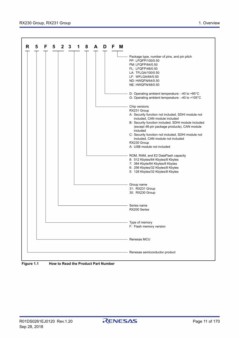
Figure 1.1 How to Read the Product Part Number
R 5 F 5 2 3 1 8 A D F M
Package type, number of pins, and pin pitchFP: LFQFP/100/0.50FM: LFQFP/64/0.50FL: LFQFP/48/0.50LA: TFLGA/100/0.50LF: WFLGA/64/0.50ND: HWQFN/64/0.50NE: HWQFN/48/0.50
D: Operating ambient temperature: –40 to +85°CG: Operating ambient temperature: –40 to +105°C
Chip versionsRX231 GroupA: Security function not included, SDHI module not
included, CAN module includedB: Security function included, SDHI module included
(except 48-pin package products), CAN module included
C: Security function not included, SDHI module not included, CAN module not included
RX230 GroupA: USB module not included
ROM, RAM, and E2 DataFlash capacity8: 512 Kbytes/64 Kbytes/8 Kbytes7: 384 Kbyte/64 Kbytes/8 Kbytes6: 256 Kbytes/32 Kbytes/8 Kbytes5: 128 Kbytes/32 Kbytes/8 Kbytes
Group name31: RX231 Group30: RX230 Group
Series nameRX200 Series
Type of memoryF: Flash memory version
Renesas MCU
Renesas semiconductor product

R01DS0261EJ0120 Rev.1.20 Page 12 of 170Sep 28, 2018
RX230 Group, RX231 Group 1. Overview
1.3 Block DiagramFigure 1.2 shows a block diagram.
Figure 1.2 Block Diagram
Clockgeneration
circuit
RX CPU
RAM
ROM
Port 0
Port 1
Port 3
Port 4
12-bit D/A converter × 2 channels
RIICa × 1 channel
DOC
RTCe
MTU2a × 6 channels
12-bit A/D converter × 24 channels
CMT × 2 channels (unit 0)
RSPIa × 1 channel
DTCa
ICUb
CAC
SCIh × 1 channel
Port 5
Port A
Port B
Port C
POE2a
USB 2.0 host/function module
Port 2
Temperature sensor
Port D
Port H
Port JExternal bus
DMACA× 4 channels
Comparator B × 4 channels
TMR × 2 channels (unit 0)
TMR × 2 channels (unit 1)
SSI
CMT × 2 channels (unit 1)
MPU
TPUa × 6 channels
Ope
rand
bus
Inst
ruct
ion
bus
Inte
rnal
mai
n bu
s 1 In
tern
al m
ain
bus
2
BSC
SCIg × 6 channels(including IrDA × 1 channel)
E2 DataFlash
CRC
ELC
IWDTa
WDTA
SDHIa
RSCAN
CTSU
LPT
Inte
rnal
per
iphe
ral b
uses
1 to
6
Port E
ICUb: Interrupt controllerDTCa: Data transfer controllerDMACA: DMA controllerBSC: Bus controllerWDTA: Watchdog timerIWDTa: Independent watchdog timerELC: Event link controllerCRC: CRC (cyclic redundancy check) calculatorSCIg/SCIh: Serial communications interfaceRSPIa: Serial peripheral interfaceSSI: Serial sound interfaceRIICa: I2C bus interfaceTPUa: 16-bit timer pulse unit
MTU2a: Multi-function timer pulse unit 2POE2a: Port output enable 2CMT: Compare match timerRTCe: Realtime clockDOC: Data operation circuitCAC: Clock frequency accuracy measurement circuitCTSU: Capacitive touch sensing unitSDHIa: SD host interfaceMPU: Memory protection unitTMR: 8-bit timerRSCAN: CAN moduleLPT: Low power timer

R01DS0261EJ0120 Rev.1.20 Page 13 of 170Sep 28, 2018
RX230 Group, RX231 Group 1. Overview
1.4 Pin FunctionsTable 1.5 lists the pin functions.
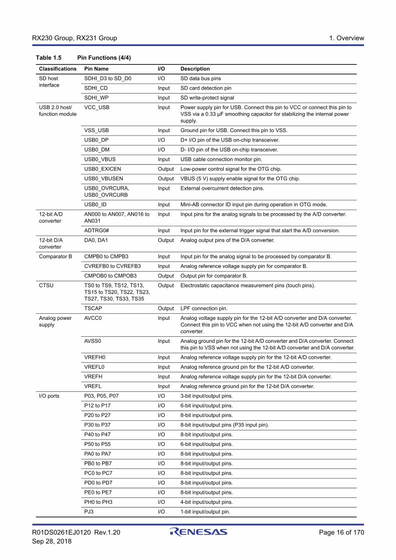
Table 1.5 Pin Functions (1/4)
Classifications Pin Name I/O Description
Power supply VCC Input Power supply pin. Connect it to the system power supply.
VCL — Connect this pin to the VSS pin via a 4.7 μF smoothing capacitor used to stabilize the internal power supply. Place the capacitor close to the pin.
VSS Input Ground pin. Connect it to the system power supply (0 V).
VBATT Input Backup power pin
Clock XTAL Output Pins for connecting a crystal. An external clock can be input through the EXTAL pin.EXTAL Input
BCLK Output Outputs the external bus clock for external devices.
XCIN Input Input/output pins for the sub-clock oscillator. Connect a crystal between XCIN and XCOUT.XCOUT Output
CLKOUT Output Clock output pin.
Operating mode control
MD Input Pin for setting the operating mode. The signal levels on this pin must not be changed during operation.
UB Input Pin used for boot mode (USB interface).
UPSEL Input Pin used for boot mode (USB interface).
System control RES# Input Reset pin. This MCU enters the reset state when this signal goes low.
CAC CACREF Input Input pin for the clock frequency accuracy measurement circuit.
On-chip emulator
FINED I/O FINE interface pin.
Address bus A0 to A23 Output Output pins for the address.
Data bus D0 to D15 I/O Input and output pins for the bidirectional data bus.
Multiplexed bus A0/D0 to A15/D15 I/O Address/data multiplexed bus
Bus control RD# Output Strobe signal which indicates that reading from the external bus interface space is in progress.
WR# Output Strobe signal which indicates that writing to the external bus interface space is in progress, in single-write strobe mode.
WR0#, WR1# Output Strobe signals which indicate that either group of data bus pins (D7 to D0, and D15 to D8) is valid in writing to the external bus interface space, in byte strobe mode.
BC0#, BC1# Output Strobe signals which indicate that either group of data bus pins (D7 to D0 and D15 to D8) is valid in access to the external bus interface space, in single-write strobe mode.
CS0# to CS3# Output Select signals for areas 0 to 3.
WAIT# Input Input pin for wait request signals in access to the external space.
ALE Output Address latch signal when address/data multiplexed bus is selected.
LVD CMPA2 Input Detection target voltage pin for voltage detection 2.
Interrupts NMI Input Non-maskable interrupt request pin.
IRQ0 to IRQ7 Input Interrupt request pins.

R01DS0261EJ0120 Rev.1.20 Page 14 of 170Sep 28, 2018
RX230 Group, RX231 Group 1. Overview
16-bit timer pulse unit
TIOCA0, TIOCB0TIOCC0, TIOCD0
I/O The TGRA0 to TGRD0 input capture input/output compare output/PWM output pins.
TIOCA1, TIOCB1 I/O The TGRA1 and TGRB1 input capture input/output compare output/PWM output pins.
TIOCA2, TIOCB2 I/O The TGRA2 and TGRB2 input capture input/output compare output/PWM output pins.
TIOCA3, TIOCB3TIOCC3, TIOCD3
I/O The TGRA3 to TGRD3 input capture input/output compare output/PWM output pins.
TIOCA4, TIOCB4 I/O The TGRA4 and TGRB4 input capture input/output compare output/PWM output pins.
TIOCA5, TIOCB5 I/O The TGRA5 and TGRB5 input capture input/output compare output/PWM output pins.
TCLKA, TCLKBTCLKC, TCLKD
Input Input pins for external clock signals.
Multi-function timer pulse unit 2
MTIOC0A, MTIOC0BMTIOC0C, MTIOC0D
I/O The TGRA0 to TGRD0 input capture input/output compare output/PWM output pins.
MTIOC1A, MTIOC1B I/O The TGRA1 and TGRB1 input capture input/output compare output/PWM output pins.
MTIOC2A, MTIOC2B I/O The TGRA2 and TGRB2 input capture input/output compare output/PWM output pins.
MTIOC3A, MTIOC3BMTIOC3C, MTIOC3D
I/O The TGRA3 to TGRD3 input capture input/output compare output/PWM output pins.
MTIOC4A, MTIOC4BMTIOC4C, MTIOC4D
I/O The TGRA4 to TGRD4 input capture input/output compare output/PWM output pins.
MTIC5U, MTIC5V, MTIC5W Input The TGRU5, TGRV5, and TGRW5 input capture input/external pulse input pins.
MTCLKA, MTCLKB, MTCLKC, MTCLKD
Input Input pins for the external clock.
Port output enable 2
POE0# to POE3#, POE8# Input Input pins for request signals to place the MTU pins in the high impedance state.
Realtime clock RTCOUT Output Output pin for the 1-Hz/64-Hz clock.
RTCIC0 to RTCIC2 Input Time capture event input pins.
8-bit timer TMO0 to TMO3 Output Compare match output pins.
TMCI0 to TMCI3 Input Input pins for the external clock to be input to the counter.
TMRI0 to TMRI3 Input Counter reset input pins.
Serial communications interface (SCIg)
• Asynchronous mode/clock synchronous mode
SCK0, SCK1, SCK5, SCK6, SCK8, SCK9
I/O Input/output pins for the clock.
RXD0, RXD1, RXD5, RXD6, RXD8, RXD9
Input Input pins for received data.
TXD0, TXD1, TXD5, TXD6, TXD8, TXD9
Output Output pins for transmitted data.
CTS0#, CTS1#, CTS5#, CTS6#, CTS8#, CTS9#
Input Input pins for controlling the start of transmission and reception.
RTS0#, RTS1#, RTS5#, RTS6#, RTS8#, RTS9#
Output Output pins for controlling the start of transmission and reception.
• Simple I2C mode
SSCL0, SSCL1, SSCL5, SSCL6, SSCL8, SSCL9
I/O Input/output pins for the I2C clock.
SSDA0, SSDA1, SSDA5, SSDA6, SSDA8, SSDA9
I/O Input/output pins for the I2C data.
Table 1.5 Pin Functions (2/4)
Classifications Pin Name I/O Description
R01DS0261EJ0120 Rev.1.20 Page 15 of 170Sep 28, 2018
RX230 Group, RX231 Group 1. Overview
Serial communications interface (SCIg)
• Simple SPI mode
SCK0, SCK1, SCK5, SCK6, SCK8, SCK9
I/O Input/output pins for the clock.
SMISO0, SMISO1, SMISO5, SMISO6, SMISO8, SMISO9
I/O Input/output pins for slave transmit data.
SMOSI0, SMOSI1, SMOSI5, SMOSI6, SMOSI8, SMOSI9
I/O Input/output pins for master transmit data.
SS0#, SS1#, SS5#, SS6#, SS8#, SS9#
Input Slave-select input pins.
IrDA interface IRTXD5 Output Data output pin in the IrDA format.
IRRXD5 Input Data input pin in the IrDA format.
Serial communications interface (SCIh)
• Asynchronous mode/clock synchronous mode
SCK12 I/O Input/output pin for the clock.
RXD12 Input Input pin for receiving data.
TXD12 Output Output pin for transmitting data.
CTS12# Input Input pin for controlling the start of transmission and reception.
RTS12# Output Output pin for controlling the start of transmission and reception.
• Simple I2C mode
SSCL12 I/O Input/output pin for the I2C clock.
SSDA12 I/O Input/output pin for the I2C data.
• Simple SPI mode
SCK12 I/O Input/output pin for the clock.
SMISO12 I/O Input/output pin for slave transmit data.
SMOSI12 I/O Input/output pin for master transmit data.
SS12# Input Slave-select input pin.
• Extended serial mode
RXDX12 Input Input pin for data reception by SCIf.
TXDX12 Output Output pin for data transmission by SCIf.
SIOX12 I/O Input/output pin for data reception or transmission by SCIf.
I2C bus interface SCL I/O Input/output pin for I2C bus interface clocks. Bus can be directly driven by the N-channel open drain output.
SDA I/O Input/output pin for I2C bus interface data. Bus can be directly driven by the N-channel open drain output.
Serial peripheral interface
RSPCKA I/O Input/output pin for the RSPI clock.
MOSIA I/O Input/output pin for transmitting data from the RSPI master.
MISOA I/O Input/output pin for transmitting data from the RSPI slave.
SSLA0 I/O Input/output pin to select the slave for the RSPI.
SSLA1 to SSLA3 Output Output pins to select the slave for the RSPI.
Serial sound interface
SSISCK0 I/O SSI serial bit clock pin.
SSIWS0 I/O Word selection pin.
SSITXD0 Output Serial data output pin.
SSIRXD0 Input Serial data input pin.
AUDIO_MCLK Input Master clock pin for audio.
CAN module CRXD0 Input Input pin
CTXD0 Output Output pin
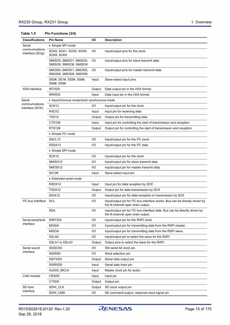
SD host interface
SDHI_CLK Output SD clock output pin
SDHI_CMD I/O SD command output, response input signal pin
Table 1.5 Pin Functions (3/4)
Classifications Pin Name I/O Description
R01DS0261EJ0120 Rev.1.20 Page 16 of 170Sep 28, 2018
RX230 Group, RX231 Group 1. Overview
SD host interface
SDHI_D3 to SD_D0 I/O SD data bus pins
SDHI_CD Input SD card detection pin
SDHI_WP Input SD write-protect signal
USB 2.0 host/function module
VCC_USB Input Power supply pin for USB. Connect this pin to VCC or connect this pin to VSS via a 0.33 µF smoothing capacitor for stabilizing the internal power supply.
VSS_USB Input Ground pin for USB. Connect this pin to VSS.
USB0_DP I/O D+ I/O pin of the USB on-chip transceiver.
USB0_DM I/O D- I/O pin of the USB on-chip transceiver.
USB0_VBUS Input USB cable connection monitor pin.
USB0_EXICEN Output Low-power control signal for the OTG chip.
USB0_VBUSEN Output VBUS (5 V) supply enable signal for the OTG chip.
USB0_OVRCURA,USB0_OVRCURB
Input External overcurrent detection pins.
USB0_ID Input Mini-AB connector ID input pin during operation in OTG mode.
12-bit A/D converter
AN000 to AN007, AN016 to AN031
Input Input pins for the analog signals to be processed by the A/D converter.
ADTRG0# Input Input pin for the external trigger signal that start the A/D conversion.
12-bit D/A converter
DA0, DA1 Output Analog output pins of the D/A converter.
Comparator B CMPB0 to CMPB3 Input Input pin for the analog signal to be processed by comparator B.
CVREFB0 to CVREFB3 Input Analog reference voltage supply pin for comparator B.
CMPOB0 to CMPOB3 Output Output pin for comparator B.
CTSU TS0 to TS9, TS12, TS13, TS15 to TS20, TS22, TS23, TS27, TS30, TS33, TS35
Output Electrostatic capacitance measurement pins (touch pins).
TSCAP Output LPF connection pin.
Analog power supply
AVCC0 Input Analog voltage supply pin for the 12-bit A/D converter and D/A converter. Connect this pin to VCC when not using the 12-bit A/D converter and D/A converter.
AVSS0 Input Analog ground pin for the 12-bit A/D converter and D/A converter. Connect this pin to VSS when not using the 12-bit A/D converter and D/A converter.
VREFH0 Input Analog reference voltage supply pin for the 12-bit A/D converter.
VREFL0 Input Analog reference ground pin for the 12-bit A/D converter.
VREFH Input Analog reference voltage supply pin for the 12-bit D/A converter.
VREFL Input Analog reference ground pin for the 12-bit D/A converter.
I/O ports P03, P05, P07 I/O 3-bit input/output pins.
P12 to P17 I/O 6-bit input/output pins.
P20 to P27 I/O 8-bit input/output pins.
P30 to P37 I/O 8-bit input/output pins (P35 input pin).
P40 to P47 I/O 8-bit input/output pins.
P50 to P55 I/O 6-bit input/output pins.
PA0 to PA7 I/O 8-bit input/output pins.
PB0 to PB7 I/O 8-bit input/output pins.
PC0 to PC7 I/O 8-bit input/output pins.
PD0 to PD7 I/O 8-bit input/output pins.
PE0 to PE7 I/O 8-bit input/output pins.
PH0 to PH3 I/O 4-bit input/output pins.
PJ3 I/O 1-bit input/output pin.
Table 1.5 Pin Functions (4/4)
Classifications Pin Name I/O Description

R01DS0261EJ0120 Rev.1.20 Page 17 of 170Sep 28, 2018
RX230 Group, RX231 Group 1. Overview
1.5 Pin AssignmentsFigure 1.3 to Figure 1.9 show the pin assignments. Table 1.6 to Table 1.10 show the lists of pins and pin functions.
Figure 1.3 Pin Assignments of the 100-Pin TFLGA (Upper Perspective View)
PE2
RX230 Group, RX231 GroupPTLG0100KA-A (100-pin TFLGA)
(Upper perspective view)
PE1 PE0 PD4 PD0 P43 VREFL0 P07 VREFH P05
PE3 PD7 PD6 PD3 PD1 P44 P40 AVCC0 AVSS0 P03
PE4 PE5 PD5 PD2 P47 P42 VREFH0 PJ3 VREFL VCL
PA0 PA1 PE7 PE6 P46 P45 VBATT MD XCOUT XCIN
PA3 PA5 PA4 PA6 PA2 P41 P34 RES# VSS P37/XTAL
VSS PA7 PB0 PB2 PB3 P12 P32 P35 VCC P36/EXTAL
VCC PB1 PB4 PB5 P52 P53 P27 P30 P31 P33
PB7 PB6 PC6 PC7 P54 P55 P15 P16 P25 P26
P17PC1 PC0 PC4 P50 VCC_USB/PH3
*1
VSS_USB/PH0
*1P13 P21 P24
PC2 PC3 PC5 P51 USB0_DP/PH1
*1
USB0_DM/PH2
*1P14 P20 P22 P23 K
J
H
G
F
E
D
C
B
A
10 9 8 7 6 5 4 3 2 1
K
J
H
G
F
E
D
C
B
A
10 9 8 7 6 5 4 3 2 1
Note: This figure indicates the power supply pins and I/O port pins. For the pin configuration, see the table “List of Pins and Pin Functions (100-Pin TFLGA)”.
Note: For the position of A1 pin in the package, see “Package Dimensions”.Note 1. RX230: PH0, PH1, PH2, PH3
RX231: VSS_USB, USB0_DP, USB0_DM, VCC_USB

R01DS0261EJ0120 Rev.1.20 Page 18 of 170Sep 28, 2018
RX230 Group, RX231 Group 1. Overview
Figure 1.4 Pin Assignments of the 100-Pin LFQFP
1 2 3 4 5 6 7 8 9 10 11 12 13 14 15 16 17 18 19 20 21 22 23 24 25
75 74 73 72 71 70 69 68 67 66 65 64 63 62 61 60 59 58 57 56 55 54 53 52 51
50
49
48
47
46
45
44
43
42
41
40
39
38
37
36
35
34
33
32
31
30
29
28
27
26
76
77
78
79
80
81
82
83
84
85
86
87
88
89
90
91
92
93
94
95
96
97
98
99
100
PE0PD7PD6PD5PD4PD3PD2PD1PD0P47P46P45
P43P42P41
VREFL0P40
VREFH0AVCC0
P07AVSS0
PE1
P44
PC2
PC4PC5PC6PC7P50P51P52P53P54P55VSS_USB/PH0*1
USB0_DP/PH1*1
VCC_USB/PH3*1
P12P13P14P15P16P17P20P21P22
PC3
USB0_DM/PH2*1
PE3
PE5
PE6
PE7
PA0
PA1
PA2
PA3
PA4
PA5
PA6
PA7
VSS
VCC
PB1
PB2
PB3
PB4
PB5
PB6
PB7
PC0
PC1
PE4
PB0
VREF
H
VREF
LPJ
3VC
LVB
ATT
MD
XCIN
XCO
UT
RES#
P37/
XTAL
VSS
P36/
EXTA
L
P35
P34
P33
P32
P31
P30
P27
P26
P25
P23
P03
VCC
PE2
P05P2
4
RX230 Group, RX231 GroupPLQP0100KB-B(100-pin LFQFP)
(Top view)
Note: This figure indicates the power supply pins and I/O port pins. For the pin configuration, see the table “List of Pins and Pin Functions (100-Pin LFQFP)”.
Note 1. RX230: PH0, PH1, PH2, PH3RX231: VSS_USB, USB0_DP, USB0_DM, VCC_USB
R01DS0261EJ0120 Rev.1.20 Page 19 of 170Sep 28, 2018
RX230 Group, RX231 Group 1. Overview
Figure 1.5 Pin Assignments of the 64-Pin WFLGA
A B C D E F G H
1
2
3
4
5
6
7
8
RX230 Group, RX231 GroupPWLG0064KA-A(64-pin WFLGA)
(Upper perspective view)
P05
AVCC0
VREFH0
AVSS0
P40
VREFL0 P41P42
P43P44VREFH
P46VREFL PE0
PE1PE2
PE3 PE4
PE5
PA0
PA1
PA3
PA4
PA6
VSS
PB0
VCC PB1
PB3
PB5
PB6 PB7
PC2PC3
PC4
PC5
PC6
PC7
P54
P55
VSS_USB/PH0
*1
USB0_DM/PH2
*1
USB0_DP/PH1
*1
VCC_USB/PH3
*1
P14
P15
P16
P17P26
P27 P30 P31
VBATT P35
VCC P36/EXTALVSS P37/
XTAL
RES#
XCOUTXCIN
MD
VCL
P03
Note: This figure indicates the power supply pins and I/O port pins. For the pin configuration, see the table “List of Pins and Pin Functions (64-Pin WFLGA)”.
Note: For the position of A1 pin in the package, see “Package Dimensions”.Note 1. RX230: PH0, PH1, PH2, PH3
RX231: VSS_USB, USB0_DP, USB0_DM, VCC_USB
R01DS0261EJ0120 Rev.1.20 Page 20 of 170Sep 28, 2018
RX230 Group, RX231 Group 1. Overview
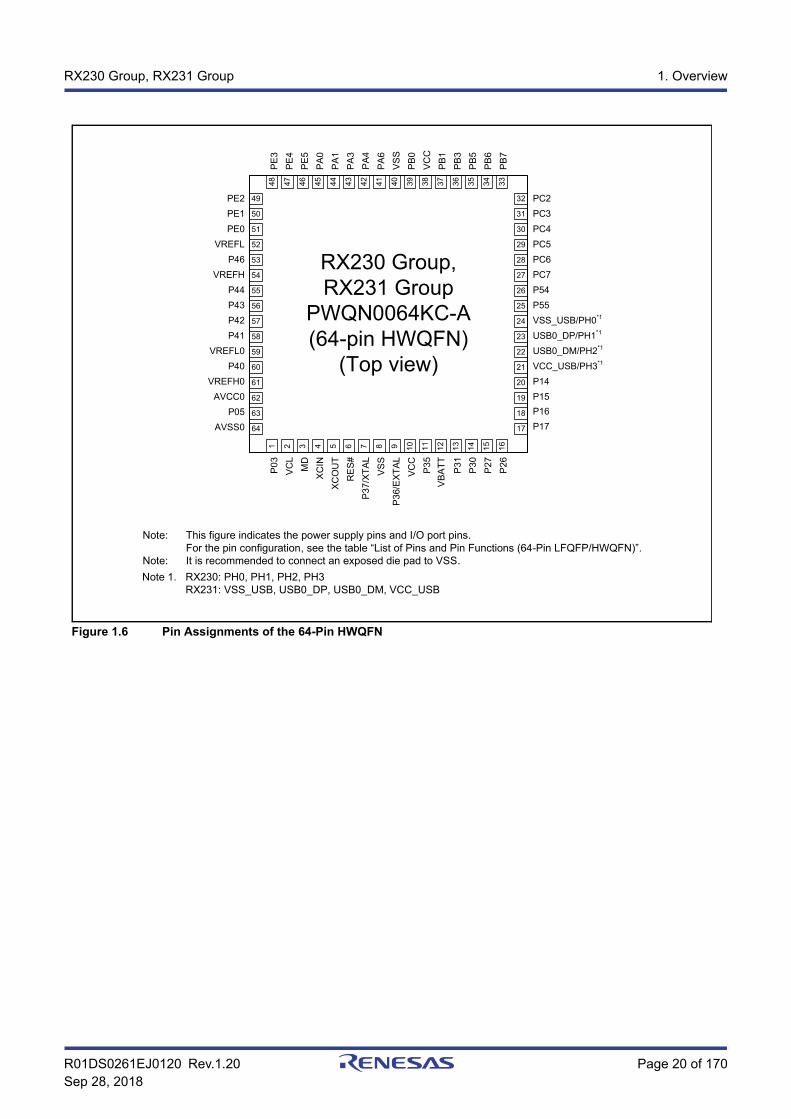
Figure 1.6 Pin Assignments of the 64-Pin HWQFN
49
RX230 Group, RX231 Group
PWQN0064KC-A(64-pin HWQFN)
(Top view)
PE2PE1PE0
VREFLP46
VREFHP44P43P42P41
VREFL0P40
VREFH0AVCC0
P05AVSS0
PE3
PE4
PE5
PA0
PA1
PA3
PA4
PA6
VSS
PB0
VCC
PB1
PB3
PB5
PB6
PB7
PC2PC3PC4PC5PC6PC7P54P55VSS_USB/PH0*1
USB0_DP/PH1*1
USB0_DM/PH2*1
VCC_USB/PH3*1
P14P15P16P17
P03
VCL
MD
XCIN
XCO
UT
RES
#P3
7/XT
ALVS
SP3
6/EX
TAL
VCC
P35
VBAT
T
P31
P30
P27
P26
64
50
51
52
53
54
55
56
57
58
59
60
61
62
63
32
17
31
30
29
28
27
26
25
24
23
22
21
20
19
18
1 162 3 4 5 6 7 8 9 10 11 12 13 14 15
48 3347 46 45 44 43 42 41 40 39 38 37 36 35 34
Note: This figure indicates the power supply pins and I/O port pins. For the pin configuration, see the table “List of Pins and Pin Functions (64-Pin LFQFP/HWQFN)”.
Note: It is recommended to connect an exposed die pad to VSS.Note 1. RX230: PH0, PH1, PH2, PH3
RX231: VSS_USB, USB0_DP, USB0_DM, VCC_USB
R01DS0261EJ0120 Rev.1.20 Page 21 of 170Sep 28, 2018
RX230 Group, RX231 Group 1. Overview
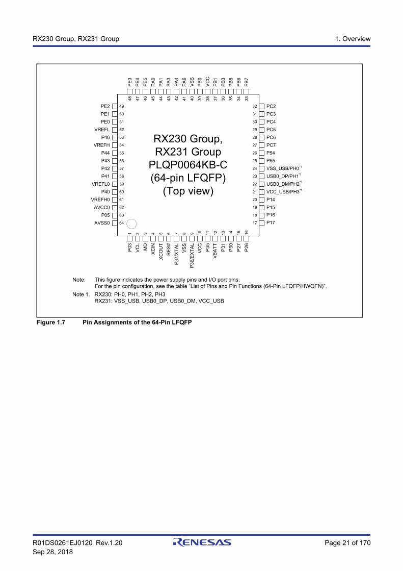
Figure 1.7 Pin Assignments of the 64-Pin LFQFP
48 47 46 45 44 43 42 41 40 39 38 37 36 35 34 33
32
31
30
29
28
27
26
25
24
23
22
21
20
19
18
17
1 2 3 4 5 6 7 8 9 10 11 12 13 14 15 16
54
55
51
49
50
52
53
56
57
58
59
60
61
63
64
62
RX230 Group, RX231 Group
PLQP0064KB-C(64-pin LFQFP)
(Top view)
PE2PE1PE0
VREFLP46
VREFHP44P43P42P41
VREFL0P40
VREFH0AVCC0
P05AVSS0
PE3
PE4
PE5
PA0
PA1
PA3
PA4
PA6
VSS
PB0
VCC
PB1
PB3
PB5
PB6
PB7
PC2PC3PC4PC5PC6PC7P54P55VSS_USB/PH0*1
USB0_DP/PH1*1
USB0_DM/PH2*1
VCC_USB/PH3*1
P14P15P16P17
P03
VCL
MD
XCIN
XCO
UT
RES
#P3
7/XT
ALVS
SP3
6/EX
TAL
VCC
P35
VBAT
T
P31
P30
P27
P26
Note: This figure indicates the power supply pins and I/O port pins. For the pin configuration, see the table “List of Pins and Pin Functions (64-Pin LFQFP/HWQFN)”.
Note 1. RX230: PH0, PH1, PH2, PH3RX231: VSS_USB, USB0_DP, USB0_DM, VCC_USB

R01DS0261EJ0120 Rev.1.20 Page 22 of 170Sep 28, 2018
RX230 Group, RX231 Group 1. Overview
Figure 1.8 Pin Assignments of the 48-Pin LFQFP
Figure 1.9 Pin Assignments of the 48-Pin HWQFN
36 35 34 33 32 31 30 29 28 27 26 25
24
23
22
21
20
19
1 2 3 4 5 6 7 8 9 10 11 12
38
39
37
40
41
42
43
44
45
47
48
46
RX230 Group, RX231 Group
PLQP0048KB-B(48-pin LFQFP)
(Top view)
PE2PE1
VREFLP46
VREFHP42P41
VREFL0P40
VREFH0AVCC0AVSS0
PE3
PE4
PA1
PA3
PA4
PA6
VSS
PB0
VCC
PB1
PB3
PB5
PC4PC5PC6PC7VSS_USB/PH0*1
USB0_DP/PH1*1
USB0_DM/PH2*1
VCC_USB/PH3*1
P14P15P16P17
VCL
MD
RES
#P3
7/XT
ALVS
SP3
6/EX
TAL
VCC
P35
P31
P30
P27
P26
18
17
16
15
14
13
Note: This figure indicates the power supply pins and I/O port pins. For the pin configuration, see the table “List of Pins and Pin Functions (48-Pin LFQFP/HWQFN)”.
Note 1. RX230: PH0, PH1, PH2, PH3RX231: VSS_USB, USB0_DP, USB0_DM, VCC_USB
RX230 Group, RX231 Group
PWQN0048KB-A(48-pin HWQFN)
(Top view)
PE2PE1
VREFLP46
VREFHP42P41
VREFL0P40
VREFH0AVCC0AVSS0
PE3
PE4
PA1
PA3
PA4
PA6
VSS
PB0
VCC
PB1
PB3
PB5
PC4PC5PC6PC7VSS_USB/PH0*1
USB0_DP/PH1*1
USB0_DM/PH2*1
VCC_USB/PH3*1
P14P15P16P17
VCL
MD
RES
#P3
7/XT
ALVS
SP3
6/EX
TAL
VCC
P35
P31
P30
P27
P26
37
48
46
45
44
43
42
41
40
39
38
47
24
13
15
16
17
18
19
20
21
22
23
14
1 121098765432 11
36 25272829303132333435 26
Note: It is recommended to connect an exposed die pad to VSS.Note: This figure indicates the power supply pins and I/O port pins.
For the pin configuration, see the table “List of Pins and Pin Functions (48-Pin LFQFP/HWQFN)”.Note 1. RX230: PH0, PH1, PH2, PH3
RX231: VSS_USB, USB0_DP, USB0_DM, VCC_USB

R01DS0261EJ0120 Rev.1.20 Page 23 of 170Sep 28, 2018
RX230 Group, RX231 Group 1. Overview
Table 1.6 List of Pins and Pin Functions (100-Pin TFLGA) (1/3)
Pin No.
Power Supply, Clock, System Control I/O Port External Bus
Timers(MTU, TPU, TMR, RTC, CMT, POE, CAC)
Communications(SCI, RSPI, RIIC, RSCAN, USB, SSI)
Memory Interface (SDHI)
Touch sensing Others
A1 P05 DA1
A2 VREFH
A3 P07 ADTRG0#
A4 VREFL0
A5 P43 AN003
A6 PD0 D0[A0/D0] IRQ0/AN024
A7 PD4 D4[A4/D4] POE3# IRQ4/AN028
A8 PE0 D8[A8/D8] SCK12 AN016
A9 PE1 D9[A9/D9] MTIOC4C TXD12/TXDX12/SIOX12/SMOSI12/SSDA12
AN017/CMPB0
A10 PE2 D10[A10/D10] MTIOC4A RXD12/RXDX12/SMISO12/SSCL12
IRQ7/AN018/CVREFB0
B1 P03 DA0
B2 AVSS0
B3 AVCC0
B4 P40 AN000
B5 P44 AN004
B6 PD1 D1[A1/D1] MTIOC4B IRQ1/AN025
B7 PD3 D3[A3/D3] POE8# IRQ3/AN027
B8 PD6 D6[A6/D6] MTIC5V/POE1# IRQ6/AN030
B9 PD7 D7[A7/D7] MTIC5U/POE0# IRQ7/AN031
B10 PE3 D11[A11/D11] MTIOC4B/POE8# CTS12#/RTS12#/SS12#/AUDIO_MCLK
AN019/CLKOUT
C1 VCL
C2 VREFL
C3 PJ3 MTIOC3C CTS6#/RTS6#/SS6#
C4 VREFH0
C5 P42 AN002
C6 P47 AN007
C7 PD2 D2[A2/D2] MTIOC4D IRQ2/AN026
C8 PD5 D5[A5/D5] MTIC5W/POE2# IRQ5/AN029
C9 PE5 D13[A13/D13] MTIOC4C/MTIOC2B IRQ5/AN021/ CMPOB0
C10 PE4 D12[A12/D12] MTIOC4D/MTIOC1A AN020/CMPA2/CLKOUT
D1 XCIN
D2 XCOUT
D3 MD FINED
D4 VBATT
D5 P45 AN005
D6 P46 AN006
D7 PE6 D14[A14/D14] IRQ6/AN022
D8 PE7 D15[A15/D15] IRQ7/AN023
D9 PA1 A1 MTIOC0B/MTCLKC/TIOCB0
SCK5/SSLA2/SSISCK0
D10 PA0 A0/BC0# MTIOC4A/TIOCA0 SSLA1 CACREF
E1 XTAL P37
E2 VSS
E3 RES#
E4 P34 MTIOC0A/TMCI3/POE2# SCK6 TS0 IRQ4
E5 P41 AN001
E6 PA2 A2 RXD5/SMISO5/SSCL5/SSLA3/IRRXD5
E7 PA6 A6 MTIC5V/MTCLKB/TMCI3/POE2#/TIOCA2
CTS5#/RTS5#/SS5#/MOSIA/SSIWS0

R01DS0261EJ0120 Rev.1.20 Page 24 of 170Sep 28, 2018
RX230 Group, RX231 Group 1. Overview
E8 PA4 A4 MTIC5U/MTCLKA/TMRI0/TIOCA1
TXD5/SMOSI5/SSDA5/SSLA0/SSITXD0/IRTXD5
IRQ5 /CVREFB1
E9 PA5 A5 TIOCB1 RSPCKA
E10 PA3 A3 MTIOC0D/MTCLKD/TIOCD0/TCLKB
RXD5/SMISO5/SSCL5/SSIRXD0/IRRXD5
IRQ6 /CMPB1
F1 EXTAL P36
F2 VCC
F3 UPSEL P35 NMI
F4 P32 MTIOC0C/TMO3/TIOCC0/RTCOUT/RTCIC2
TXD6/SMOSI6/SSDA6/USB0_VBUSEN
IRQ2
F5 P12 TMCI1 SCL IRQ2
F6 PB3 A11 MTIOC0A/MTIOC4A/TMO0/POE3#/TIOCD3/TCLKD
SCK6 SDHI_WP
F7 PB2 A10 TIOCC3/TCLKC CTS6#/RTS6#/SS6#
F8 PB0 A8 MTIC5W/TIOCA3 RXD6/SMISO6/SSCL6/RSPCKA
SDHI_CMD
F9 PA7 A7 TIOCB2 MISOA
F10 VSS
G1 P33 MTIOC0D/TMRI3/POE3#/TIOCD0
RXD6/SMISO6/SSCL6 TS1 IRQ3
G2 P31 MTIOC4D/TMCI2/RTCIC1 CTS1#/RTS1#/SS1#/SSISCK0
IRQ1
G3 P30 MTIOC4B/TMRI3/POE8#/RTCIC0
RXD1/SMISO1/SSCL1/AUDIO_MCLK
IRQ0/CMPOB3
G4 P27 CS3# MTIOC2B/TMCI3 SCK1/ SSIWS0 TS2 CVREFB3
G5 BCLK P53 TS17
G6 P52 RD# TS18
G7 PB5 A13 MTIOC2A/MTIOC1B/TMRI1/POE1#/TIOCB4
SCK9/USB0_VBUS SDHI_CD
G8 PB4 A12 TIOCA4 CTS9#/RTS9#/SS9#
G9 PB1 A9 MTIOC0C/MTIOC4C/TMCI0/TIOCB3
TXD6/SMOSI6/SSDA6 SDHI_CLK
IRQ4/ CMPOB1
G10 VCC
H1 P26 CS2# MTIOC2A/TMO1 TXD1/SMOSI1/SSDA1/ SSIRXD0
TS3 CMPB3
H2 P25 CS1# MTIOC4C/MTCLKB/TIOCA4
TS4 ADTRG0#
H3 P16 MTIOC3C/MTIOC3D/TMO2/TIOCB1/TCLKC/RTCOUT
TXD1/SMOSI1/SSDA1/MOSIA/SCL/USB0_VBUS/USB0_VBUSEN/USB0_OVRCURB
IRQ6/ADTRG0#
H4 P15 MTIOC0B/MTCLKB/TMCI2/TIOCB2/TCLKB
RXD1/SMISO1/SSCL1/CRXD0
TS12 IRQ5/CMPB2
H5 P55 WAIT# MTIOC4D/TMO3 CRXD0 TS15
H6 P54 ALE MTIOC4B/TMCI1 CTXD0 TS16
H7 UB PC7 A23/CS0# MTIOC3A/MTCLKB/TMO2 TXD8/SMOSI8/SSDA8/MISOA
CACREF
H8 PC6 A22/CS1# MTIOC3C/MTCLKA/TMCI2 RXD8/SMISO8/SSCL8/MOSIA
TS22
H9 PB6 A14 MTIOC3D/TIOCA5 RXD9/SMISO9/SSCL9 SDHI_D1
H10 PB7 A15 MTIOC3B/TIOCB5 TXD9/SMOSI9/SSDA9 SDHI_D2
J1 P24 CS0# MTIOC4A/MTCLKA/TMRI1/TIOCB4
USB0_VBUSEN TS5
J2 P21 MTIOC1B/TMCI0/TIOCA3 RXD0/SMISO0/SSCL0/USB0_EXICEN/SSIWS0
TS8
J3 P17 MTIOC3A/MTIOC3B/TMO1/POE8#/TIOCB0/TCLKD
SCK1/MISOA/SDA/ SSITXD0
IRQ7/ CMPOB2
J4 P13 MTIOC0B/TMO3/TIOCA5 SDA IRQ3
J5 VSS_USB*1 PH0*1 CACREF*1
Table 1.6 List of Pins and Pin Functions (100-Pin TFLGA) (2/3)
Pin No.
Power Supply, Clock, System Control I/O Port External Bus
Timers(MTU, TPU, TMR, RTC, CMT, POE, CAC)
Communications(SCI, RSPI, RIIC, RSCAN, USB, SSI)
Memory Interface (SDHI)
Touch sensing Others

R01DS0261EJ0120 Rev.1.20 Page 25 of 170Sep 28, 2018
RX230 Group, RX231 Group 1. Overview
Note 1. RX230: PH0/CACREF, PH1/IRQ0/TMO0, PH2/IRQ1/TMRI0, PH3/TMCI0RX231: VSS_USB, USB0_DP, USB0_DM, VCC_USB
J6 VCC_USB*1 PH3*1 TMCI0*1
J7 P50 WR0#/WR# TS20
J8 PC4 A20/CS3# MTIOC3D/MTCLKC/TMCI1/POE0#
SCK5/CTS8#/RTS8#/SS8#/SSLA0
SDHI_D1 TSCAP
J9 PC0 A16 MTIOC3C/TCLKC CTS5#/RTS5#/SS5#/SSLA1
TS35
J10 PC1 A17 MTIOC3A/TCLKD SCK5/SSLA2 TS33
K1 P23 MTIOC3D/MTCLKD/TIOCD3
CTS0#/RTS0#/SS0#/ SSISCK0
TS6
K2 P22 MTIOC3B/MTCLKC/TMO0/TIOCC3
SCK0/ USB0_OVRCURB/AUDIO_MCLK
TS7
K3 P20 MTIOC1A/TMRI0/TIOCB3 TXD0/SMOSI0/SSDA0/USB0_ID/SSIRXD0
TS9
K4 P14 MTIOC3A/MTCLKA/TMRI2/TIOCB5/TCLKA
CTS1#/RTS1#/SS1#/CTXD0/USB0_OVRCURA
TS13 IRQ4/CVREFB2
K5 PH2*1 TMRI0*1 USB0_DM*1 IRQ1*1
K6 PH1*1 TMO0*1 USB0_DP*1 IRQ0*1
K7 P51 WR1#/BC1#/WAIT#
TS19
K8 PC5 A21/CS2#/WAIT#
MTIOC3B/MTCLKD/TMRI2 SCK8/RSPCKA TS23
K9 PC3 A19 MTIOC4D/TCLKB TXD5/SMOSI5/SSDA5/ IRTXD5
SDHI_D0 TS27
K10 PC2 A18 MTIOC4B/TCLKA RXD5/SMISO5/SSCL5/SSLA3/ IRRXD5
SDHI_D3 TS30
Table 1.6 List of Pins and Pin Functions (100-Pin TFLGA) (3/3)
Pin No.
Power Supply, Clock, System Control I/O Port External Bus
Timers(MTU, TPU, TMR, RTC, CMT, POE, CAC)
Communications(SCI, RSPI, RIIC, RSCAN, USB, SSI)
Memory Interface (SDHI)
Touch sensing Others

R01DS0261EJ0120 Rev.1.20 Page 26 of 170Sep 28, 2018
RX230 Group, RX231 Group 1. Overview
Table 1.7 List of Pins and Pin Functions (100-Pin LFQFP) (1/3)
Pin No.
Power Supply, Clock, System Control I/O Port External Bus
Timers(MTU, TPU, TMR, RTC, CMT, POE, CAC)
Communications(SCI, RSPI, RIIC, RSCAN, USB, SSI)
Memory Interface (SDHI)
Touch sensing Others
1 VREFH
2 P03 DA0
3 VREFL
4 PJ3 MTIOC3C CTS6#/RTS6#/SS6#
5 VCL
6 VBATT
7 MD FINED
8 XCIN
9 XCOUT
10 RES#
11 XTAL P37
12 VSS
13 EXTAL P36
14 VCC
15 UPSEL P35 NMI
16 P34 MTIOC0A/TMCI3/POE2# SCK6 TS0 IRQ4
17 P33 MTIOC0D/TMRI3/POE3#/TIOCD0
RXD6/SMISO6/SSCL6 TS1 IRQ3
18 P32 MTIOC0C/TMO3/TIOCC0/RTCOUT/RTCIC2
TXD6/SMOSI6/SSDA6/USB0_VBUSEN
IRQ2
19 P31 MTIOC4D/TMCI2/RTCIC1 CTS1#/RTS1#/SS1#/SSISCK0
IRQ1
20 P30 MTIOC4B/TMRI3/POE8#/RTCIC0
RXD1/SMISO1/SSCL1/AUDIO_MCLK
IRQ0/CMPOB3
21 P27 CS3# MTIOC2B/TMCI3 SCK1/ SSIWS0 TS2 CVREFB3
22 P26 CS2# MTIOC2A/TMO1 TXD1/SMOSI1/SSDA1/ SSIRXD0
TS3 CMPB3
23 P25 CS1# MTIOC4C/MTCLKB/TIOCA4
TS4 ADTRG0#
24 P24 CS0# MTIOC4A/MTCLKA/TMRI1/TIOCB4
USB0_VBUSEN TS5
25 P23 MTIOC3D/MTCLKD/TIOCD3
CTS0#/RTS0#/SS0#/ SSISCK0
TS6
26 P22 MTIOC3B/MTCLKC/TMO0/TIOCC3
SCK0/ USB0_OVRCURB/AUDIO_MCLK
TS7
27 P21 MTIOC1B/TMCI0/TIOCA3 RXD0/SMISO0/SSCL0/USB0_EXICEN/SSIWS0
TS8
28 P20 MTIOC1A/TMRI0/TIOCB3 TXD0/SMOSI0/SSDA0/USB0_ID/SSIRXD0
TS9
29 P17 MTIOC3A/MTIOC3B/TMO1/POE8#/TIOCB0/TCLKD
SCK1/MISOA/SDA/ SSITXD0
IRQ7/ CMPOB2
30 P16 MTIOC3C/MTIOC3D/TMO2/TIOCB1/TCLKC/RTCOUT
TXD1/SMOSI1/SSDA1/MOSIA/SCL/USB0_VBUS/USB0_VBUSEN/USB0_OVRCURB
IRQ6/ADTRG0#
31 P15 MTIOC0B/MTCLKB/TMCI2/TIOCB2/TCLKB
RXD1/SMISO1/SSCL1/CRXD0
TS12 IRQ5/CMPB2
32 P14 MTIOC3A/MTCLKA/TMRI2/TIOCB5/TCLKA
CTS1#/RTS1#/SS1#/CTXD0/USB0_OVRCURA
TS13 IRQ4/CVREFB2
33 P13 MTIOC0B/TMO3/TIOCA5 SDA IRQ3
34 P12 TMCI1 SCL IRQ2
35 VCC_USB*1 PH3*1 TMCI0*1
36 PH2*1 TMRI0*1 USB0_DM*1 IRQ1*1
37 PH1*1 TMO0*1 USB0_DP*1 IRQ0*1
38 VSS_USB*1 PH0*1 CACREF*1
39 P55 WAIT# MTIOC4D/TMO3 CRXD0 TS15
40 P54 ALE MTIOC4B/TMCI1 CTXD0 TS16
41 BCLK P53 TS17
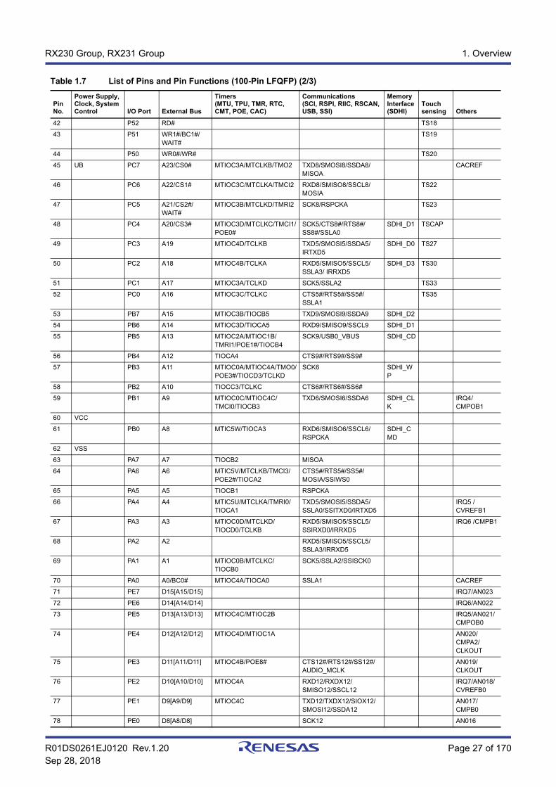
R01DS0261EJ0120 Rev.1.20 Page 27 of 170Sep 28, 2018
RX230 Group, RX231 Group 1. Overview
42 P52 RD# TS18
43 P51 WR1#/BC1#/WAIT#
TS19
44 P50 WR0#/WR# TS20
45 UB PC7 A23/CS0# MTIOC3A/MTCLKB/TMO2 TXD8/SMOSI8/SSDA8/MISOA
CACREF
46 PC6 A22/CS1# MTIOC3C/MTCLKA/TMCI2 RXD8/SMISO8/SSCL8/MOSIA
TS22
47 PC5 A21/CS2#/WAIT#
MTIOC3B/MTCLKD/TMRI2 SCK8/RSPCKA TS23
48 PC4 A20/CS3# MTIOC3D/MTCLKC/TMCI1/POE0#
SCK5/CTS8#/RTS8#/SS8#/SSLA0
SDHI_D1 TSCAP
49 PC3 A19 MTIOC4D/TCLKB TXD5/SMOSI5/SSDA5/ IRTXD5
SDHI_D0 TS27
50 PC2 A18 MTIOC4B/TCLKA RXD5/SMISO5/SSCL5/SSLA3/ IRRXD5
SDHI_D3 TS30
51 PC1 A17 MTIOC3A/TCLKD SCK5/SSLA2 TS33
52 PC0 A16 MTIOC3C/TCLKC CTS5#/RTS5#/SS5#/SSLA1
TS35
53 PB7 A15 MTIOC3B/TIOCB5 TXD9/SMOSI9/SSDA9 SDHI_D2
54 PB6 A14 MTIOC3D/TIOCA5 RXD9/SMISO9/SSCL9 SDHI_D1
55 PB5 A13 MTIOC2A/MTIOC1B/TMRI1/POE1#/TIOCB4
SCK9/USB0_VBUS SDHI_CD
56 PB4 A12 TIOCA4 CTS9#/RTS9#/SS9#
57 PB3 A11 MTIOC0A/MTIOC4A/TMO0/POE3#/TIOCD3/TCLKD
SCK6 SDHI_WP
58 PB2 A10 TIOCC3/TCLKC CTS6#/RTS6#/SS6#
59 PB1 A9 MTIOC0C/MTIOC4C/TMCI0/TIOCB3
TXD6/SMOSI6/SSDA6 SDHI_CLK
IRQ4/ CMPOB1
60 VCC
61 PB0 A8 MTIC5W/TIOCA3 RXD6/SMISO6/SSCL6/RSPCKA
SDHI_CMD
62 VSS
63 PA7 A7 TIOCB2 MISOA
64 PA6 A6 MTIC5V/MTCLKB/TMCI3/POE2#/TIOCA2
CTS5#/RTS5#/SS5#/MOSIA/SSIWS0
65 PA5 A5 TIOCB1 RSPCKA
66 PA4 A4 MTIC5U/MTCLKA/TMRI0/TIOCA1
TXD5/SMOSI5/SSDA5/SSLA0/SSITXD0/IRTXD5
IRQ5 /CVREFB1
67 PA3 A3 MTIOC0D/MTCLKD/TIOCD0/TCLKB
RXD5/SMISO5/SSCL5/SSIRXD0/IRRXD5
IRQ6 /CMPB1
68 PA2 A2 RXD5/SMISO5/SSCL5/SSLA3/IRRXD5
69 PA1 A1 MTIOC0B/MTCLKC/TIOCB0
SCK5/SSLA2/SSISCK0
70 PA0 A0/BC0# MTIOC4A/TIOCA0 SSLA1 CACREF
71 PE7 D15[A15/D15] IRQ7/AN023
72 PE6 D14[A14/D14] IRQ6/AN022
73 PE5 D13[A13/D13] MTIOC4C/MTIOC2B IRQ5/AN021/ CMPOB0
74 PE4 D12[A12/D12] MTIOC4D/MTIOC1A AN020/CMPA2/CLKOUT
75 PE3 D11[A11/D11] MTIOC4B/POE8# CTS12#/RTS12#/SS12#/AUDIO_MCLK
AN019/CLKOUT
76 PE2 D10[A10/D10] MTIOC4A RXD12/RXDX12/SMISO12/SSCL12
IRQ7/AN018/CVREFB0
77 PE1 D9[A9/D9] MTIOC4C TXD12/TXDX12/SIOX12/SMOSI12/SSDA12
AN017/CMPB0
78 PE0 D8[A8/D8] SCK12 AN016
Table 1.7 List of Pins and Pin Functions (100-Pin LFQFP) (2/3)
Pin No.
Power Supply, Clock, System Control I/O Port External Bus
Timers(MTU, TPU, TMR, RTC, CMT, POE, CAC)
Communications(SCI, RSPI, RIIC, RSCAN, USB, SSI)
Memory Interface (SDHI)
Touch sensing Others

R01DS0261EJ0120 Rev.1.20 Page 28 of 170Sep 28, 2018
RX230 Group, RX231 Group 1. Overview
Note 1. RX230: PH0/CACREF, PH1/IRQ0/TMO0, PH2/IRQ1/TMRI0, PH3/TMCI0RX231: VSS_USB, USB0_DP, USB0_DM, VCC_USB
79 PD7 D7[A7/D7] MTIC5U/POE0# IRQ7/AN031
80 PD6 D6[A6/D6] MTIC5V/POE1# IRQ6/AN030
81 PD5 D5[A5/D5] MTIC5W/POE2# IRQ5/AN029
82 PD4 D4[A4/D4] POE3# IRQ4/AN028
83 PD3 D3[A3/D3] POE8# IRQ3/AN027
84 PD2 D2[A2/D2] MTIOC4D IRQ2/AN026
85 PD1 D1[A1/D1] MTIOC4B IRQ1/AN025
86 PD0 D0[A0/D0] IRQ0/AN024
87 P47 AN007
88 P46 AN006
89 P45 AN005
90 P44 AN004
91 P43 AN003
92 P42 AN002
93 P41 AN001
94 VREFL0
95 P40 AN000
96 VREFH0
97 AVCC0
98 P07 ADTRG0#
99 AVSS0
100 P05 DA1
Table 1.7 List of Pins and Pin Functions (100-Pin LFQFP) (3/3)
Pin No.
Power Supply, Clock, System Control I/O Port External Bus
Timers(MTU, TPU, TMR, RTC, CMT, POE, CAC)
Communications(SCI, RSPI, RIIC, RSCAN, USB, SSI)
Memory Interface (SDHI)
Touch sensing Others
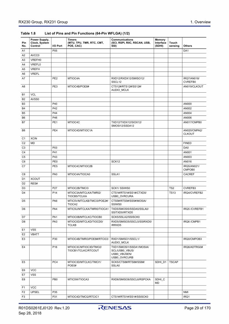
R01DS0261EJ0120 Rev.1.20 Page 29 of 170Sep 28, 2018
RX230 Group, RX231 Group 1. Overview
Table 1.8 List of Pins and Pin Functions (64-Pin WFLGA) (1/2)
Pin No.
Power Supply, Clock, System Control I/O Port
Timers(MTU, TPU, TMR, RTC, CMT, POE, CAC)
Communications(SCI, RSPI, RIIC, RSCAN, USB, SSI)
Memory Interface (SDHI)
Touch sensing Others
A1 P05 DA1
A2 AVCC0
A3 VREFH0
A4 VREFL0
A5 VREFH
A6 VREFL
A7 PE2 MTIOC4A RXD12/RXDX12/SMISO12/SSCL12
IRQ7/AN018/CVREFB0
A8 PE3 MTIOC4B/POE8# CTS12#/RTS12#/SS12#/AUDIO_MCLK
AN019/CLKOUT
B1 VCL
B2 AVSS0
B3 P40 AN000
B4 P42 AN002
B5 P44 AN004
B6 P46 AN006
B7 PE1 MTIOC4C TXD12/TXDX12/SIOX12/SMOSI12/SSDA12
AN017/CMPB0
B8 PE4 MTIOC4D/MTIOC1A AN020/CMPA2/CLKOUT
C1 XCIN
C2 MD FINED
C3 P03 DA0
C4 P41 AN001
C5 P43 AN003
C6 PE0 SCK12 AN016
C7 PE5 MTIOC4C/MTIOC2B IRQ5/AN021/ CMPOB0
C8 PA0 MTIOC4A/TIOCA0 SSLA1 CACREF
D1 XCOUT
D2 RES#
D3 P27 MTIOC2B/TMCI3 SCK1/ SSIWS0 TS2 CVREFB3
D4 P14 MTIOC3A/MTCLKA/TMRI2/TIOCB5/TCLKA
CTS1#/RTS1#/SS1#/CTXD0/ USB0_OVRCURA
TS13 IRQ4/CVREFB2
D5 PA6 MTIC5V/MTCLKB/TMCI3/POE2#/TIOCA2
CTS5#/RTS5#/SS5#/MOSIA/SSIWS0
D6 PA4 MTIC5U/MTCLKA/TMRI0/TIOCA1 TXD5/SMOSI5/SSDA5/SSLA0/SSITXD0/IRTXD5
IRQ5 /CVREFB1
D7 PA1 MTIOC0B/MTCLKC/TIOCB0 SCK5/SSLA2/SSISCK0
D8 PA3 MTIOC0D/MTCLKD/TIOCD0/TCLKB
RXD5/SMISO5/SSCL5/SSIRXD0/IRRXD5
IRQ6 /CMPB1
E1 VSS
E2 VBATT
E3 P30 MTIOC4B/TMRI3/POE8#/RTCIC0 RXD1/SMISO1/SSCL1/AUDIO_MCLK
IRQ0/CMPOB3
E4 P16 MTIOC3C/MTIOC3D/TMO2/TIOCB1/TCLKC/RTCOUT
TXD1/SMOSI1/SSDA1/MOSIA/SCL/USB0_VBUS/USB0_VBUSEN/USB0_OVRCURB
IRQ6/ADTRG0#
E5 PC4 MTIOC3D/MTCLKC/TMCI1/POE0#
SCK5/CTS8#/RTS8#/SS8#/SSLA0
SDHI_D1 TSCAP
E6 VCC
E7 VSS
E8 PB0 MTIC5W/TIOCA3 RXD6/SMISO6/SSCL6/RSPCKA SDHI_CMD
F1 VCC
F2 UPSEL P35 NMI
F3 P31 MTIOC4D/TMCI2/RTCIC1 CTS1#/RTS1#/SS1#/SSISCK0 IRQ1

R01DS0261EJ0120 Rev.1.20 Page 30 of 170Sep 28, 2018
RX230 Group, RX231 Group 1. Overview
Note 1. RX230: PH0/CACREF, PH1/IRQ0/TMO0, PH2/IRQ1/TMRI0, PH3/TMCI0RX231: VSS_USB, USB0_DP, USB0_DM, VCC_USB
F4 PC5 MTIOC3B/MTCLKD/TMRI2 SCK8/RSPCKA/USB0_ID TS23
F5 P15 MTIOC0B/MTCLKB/TMCI2/TIOCB2/TCLKB
RXD1/SMISO1/SSCL1/CRXD0 TS12 IRQ5/CMPB2
F6 PB1 MTIOC0C/MTIOC4C/TMCI0/TIOCB3
TXD6/SMOSI6/SSDA6 SDHI_CLK
IRQ4/ CMPOB1
F7 PB5 MTIOC2A/MTIOC1B/TMRI1/POE1#/TIOCB4
SCK9/USB0_VBUS SDHI_CD
F8 PB3 MTIOC0A/MTIOC4A/TMO0/POE3#/TIOCD3/TCLKD
SCK6 SDHI_WP
G1 EXTAL P36
G2 P26 MTIOC2A/TMO1 TXD1/SMOSI1/SSDA1/ USB0_VBUSEN/SSIRXD0
TS3 CMPB3
G3 VCC_USB*1 PH3*1 TMCI0*1
G4 VSS_USB*1 PH0*1 CACREF*1
G5 UB PC7 MTIOC3A/MTCLKB/TMO2 TXD8/SMOSI8/SSDA8/MISOA CACREF
G6 PC6 MTIOC3C/MTCLKA/TMCI2 RXD8/SMISO8/SSCL8/MOSIA/USB0_EXICEN
TS22
G7 PC3 MTIOC4D/TCLKB TXD5/SMOSI5/SSDA5/IRTXD5 SDHI_D0 TS27
G8 PB6/PC0 MTIOC3D/TIOCA5 RXD9/SMISO9/SSCL9 SDHI_D1
H1 XTAL P37
H2 P17 MTIOC3A/MTIOC3B/TMO1/POE8#/TIOCB0/TCLKD
SCK1/MISOA/SDA/SSITXD0 IRQ7/ CMPOB2
H3 PH2*1 TMRI0*1 USB0_DM*1 IRQ1*1
H4 PH1*1 TMO0*1 USB0_DP*1 IRQ0*1
H5 P55 MTIOC4D/TMO3 CRXD0 TS15
H6 P54 MTIOC4B/TMCI1 CTXD0 TS16
H7 PC2 MTIOC4B/TCLKA RXD5/SMISO5/SSCL5/SSLA3/ IRRXD5
SDHI_D3 TS30
H8 PB7/PC1 MTIOC3B/TIOCB5 TXD9/SMOSI9/SSDA9 SDHI_D2
Table 1.8 List of Pins and Pin Functions (64-Pin WFLGA) (2/2)
Pin No.
Power Supply, Clock, System Control I/O Port
Timers(MTU, TPU, TMR, RTC, CMT, POE, CAC)
Communications(SCI, RSPI, RIIC, RSCAN, USB, SSI)
Memory Interface (SDHI)
Touch sensing Others

R01DS0261EJ0120 Rev.1.20 Page 31 of 170Sep 28, 2018
RX230 Group, RX231 Group 1. Overview
Table 1.9 List of Pins and Pin Functions (64-Pin LFQFP/HWQFN) (1/2)
Pin No.
Power Supply, Clock, System Control I/O Port
Timers(MTU, TPU, TMR, RTC, CMT, POE, CAC)
Communications(SCI, RSPI, RIIC, RSCAN, USB, SSI)
Memory Interface (SDHI)
Touch sensing Others
1 P03 DA0
2 VCL
3 MD FINED
4 XCIN
5 XCOUT
6 RES#
7 XTAL P37
8 VSS
9 EXTAL P36
10 VCC
11 UPSEL P35 NMI
12 VBATT
13 P31 MTIOC4D/TMCI2/RTCIC1 CTS1#/RTS1#/SS1#/SSISCK0 IRQ1
14 P30 MTIOC4B/TMRI3/POE8#/RTCIC0 RXD1/SMISO1/SSCL1/AUDIO_MCLK
IRQ0/CMPOB3
15 P27 MTIOC2B/TMCI3 SCK1/SSIWS0 TS2 CVREFB3
16 P26 MTIOC2A/TMO1 TXD1/SMOSI1/SSDA1/ USB0_VBUSEN/SSIRXD0
TS3 CMPB3
17 P17 MTIOC3A/MTIOC3B/TMO1/POE8#/TIOCB0/TCLKD
SCK1/MISOA/SDA/SSITXD0 IRQ7/ CMPOB2
18 P16 MTIOC3C/MTIOC3D/TMO2/TIOCB1/TCLKC/RTCOUT
TXD1/SMOSI1/SSDA1/MOSIA/SCL/USB0_VBUS/USB0_VBUSEN/USB0_OVRCURB
IRQ6/ADTRG0#
19 P15 MTIOC0B/MTCLKB/TMCI2/TIOCB2/TCLKB
RXD1/SMISO1/SSCL1/CRXD0 TS12 IRQ5/CMPB2
20 P14 MTIOC3A/MTCLKA/TMRI2/TIOCB5/TCLKA
CTS1#/RTS1#/SS1#/CTXD0/ USB0_OVRCURA
TS13 IRQ4/CVREFB2
21 VCC_USB*1 PH3*1 TMCI0*1
22 PH2*1 TMRI0*1 USB0_DM*1 IRQ1*1
23 PH1*1 TMO0*1 USB0_DP*1 IRQ0*1
24 VSS_USB*1 PH0*1 CACREF*1
25 P55 MTIOC4D/TMO3 CRXD0 TS15
26 P54 MTIOC4B/TMCI1 CTXD0 TS16
27 UB PC7 MTIOC3A/MTCLKB/TMO2 TXD8/SMOSI8/SSDA8/MISOA CACREF
28 PC6 MTIOC3C/MTCLKA/TMCI2 RXD8/SMISO8/SSCL8/MOSIA/USB0_EXICEN
TS22
29 PC5 MTIOC3B/MTCLKD/TMRI2 SCK8/RSPCKA/USB0_ID TS23
30 PC4 MTIOC3D/MTCLKC/TMCI1/POE0#
SCK5/CTS8#/RTS8#/SS8#/SSLA0
SDHI_D1 TSCAP
31 PC3 MTIOC4D/TCLKB TXD5/SMOSI5/SSDA5/ IRTXD5 SDHI_D0 TS27
32 PC2 MTIOC4B/TCLKA RXD5/SMISO5/SSCL5/SSLA3/ IRRXD5
SDHI_D3 TS30
33 PB7/PC1 MTIOC3B/TIOCB5 TXD9/SMOSI9/SSDA9 SDHI_D2
34 PB6/PC0 MTIOC3D/TIOCA5 RXD9/SMISO9/SSCL9 SDHI_D1
35 PB5 MTIOC2A/MTIOC1B/TMRI1/POE1#/TIOCB4
SCK9/USB0_VBUS SDHI_CD
36 PB3 MTIOC0A/MTIOC4A/TMO0/POE3#/TIOCD3/TCLKD
SCK6 SDHI_WP
37 PB1 MTIOC0C/MTIOC4C/TMCI0/TIOCB3
TXD6/SMOSI6/SSDA6 SDHI_CLK
IRQ4/ CMPOB1
38 VCC
39 PB0 MTIC5W/TIOCA3 RXD6/SMISO6/SSCL6/RSPCKA SDHI_CMD
40 VSS
41 PA6 MTIC5V/MTCLKB/TMCI3/POE2#/TIOCA2
CTS5#/RTS5#/SS5#/MOSIA/SSIWS0
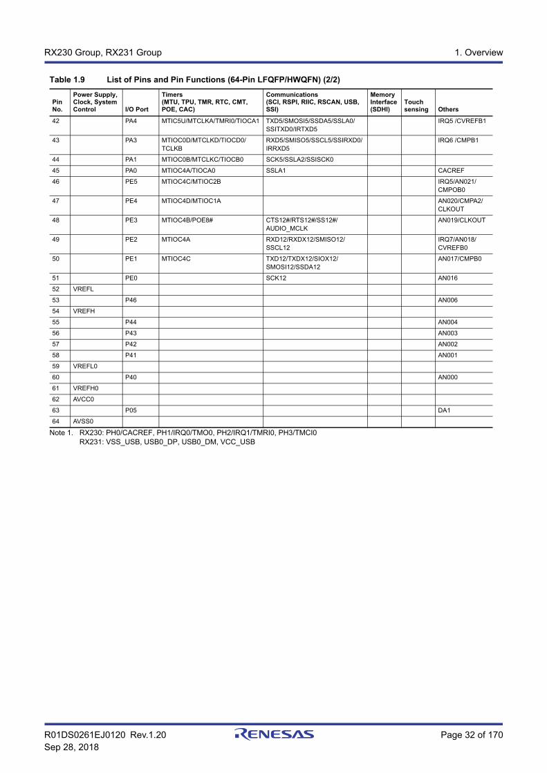
R01DS0261EJ0120 Rev.1.20 Page 32 of 170Sep 28, 2018
RX230 Group, RX231 Group 1. Overview
Note 1. RX230: PH0/CACREF, PH1/IRQ0/TMO0, PH2/IRQ1/TMRI0, PH3/TMCI0RX231: VSS_USB, USB0_DP, USB0_DM, VCC_USB
42 PA4 MTIC5U/MTCLKA/TMRI0/TIOCA1 TXD5/SMOSI5/SSDA5/SSLA0/SSITXD0/IRTXD5
IRQ5 /CVREFB1
43 PA3 MTIOC0D/MTCLKD/TIOCD0/TCLKB
RXD5/SMISO5/SSCL5/SSIRXD0/IRRXD5
IRQ6 /CMPB1
44 PA1 MTIOC0B/MTCLKC/TIOCB0 SCK5/SSLA2/SSISCK0
45 PA0 MTIOC4A/TIOCA0 SSLA1 CACREF
46 PE5 MTIOC4C/MTIOC2B IRQ5/AN021/ CMPOB0
47 PE4 MTIOC4D/MTIOC1A AN020/CMPA2/CLKOUT
48 PE3 MTIOC4B/POE8# CTS12#/RTS12#/SS12#/AUDIO_MCLK
AN019/CLKOUT
49 PE2 MTIOC4A RXD12/RXDX12/SMISO12/SSCL12
IRQ7/AN018/CVREFB0
50 PE1 MTIOC4C TXD12/TXDX12/SIOX12/SMOSI12/SSDA12
AN017/CMPB0
51 PE0 SCK12 AN016
52 VREFL
53 P46 AN006
54 VREFH
55 P44 AN004
56 P43 AN003
57 P42 AN002
58 P41 AN001
59 VREFL0
60 P40 AN000
61 VREFH0
62 AVCC0
63 P05 DA1
64 AVSS0
Table 1.9 List of Pins and Pin Functions (64-Pin LFQFP/HWQFN) (2/2)
Pin No.
Power Supply, Clock, System Control I/O Port
Timers(MTU, TPU, TMR, RTC, CMT, POE, CAC)
Communications(SCI, RSPI, RIIC, RSCAN, USB, SSI)
Memory Interface (SDHI)
Touch sensing Others
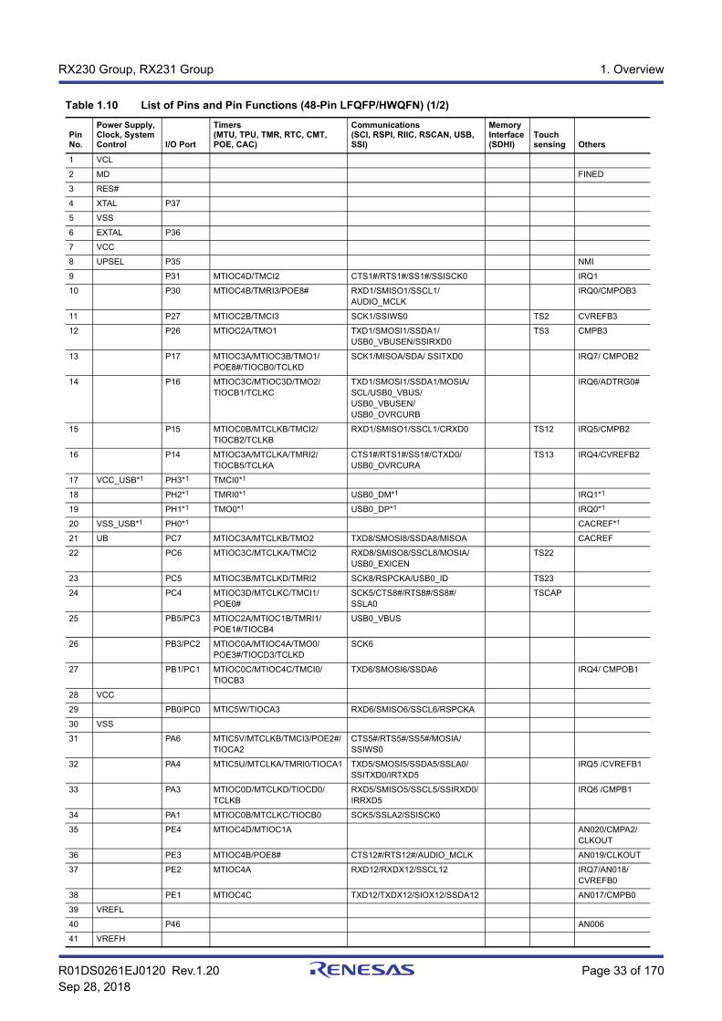
R01DS0261EJ0120 Rev.1.20 Page 33 of 170Sep 28, 2018
RX230 Group, RX231 Group 1. Overview
Table 1.10 List of Pins and Pin Functions (48-Pin LFQFP/HWQFN) (1/2)
Pin No.
Power Supply, Clock, System Control I/O Port
Timers(MTU, TPU, TMR, RTC, CMT, POE, CAC)
Communications(SCI, RSPI, RIIC, RSCAN, USB, SSI)
Memory Interface (SDHI)
Touch sensing Others
1 VCL
2 MD FINED
3 RES#
4 XTAL P37
5 VSS
6 EXTAL P36
7 VCC
8 UPSEL P35 NMI
9 P31 MTIOC4D/TMCI2 CTS1#/RTS1#/SS1#/SSISCK0 IRQ1
10 P30 MTIOC4B/TMRI3/POE8# RXD1/SMISO1/SSCL1/AUDIO_MCLK
IRQ0/CMPOB3
11 P27 MTIOC2B/TMCI3 SCK1/SSIWS0 TS2 CVREFB3
12 P26 MTIOC2A/TMO1 TXD1/SMOSI1/SSDA1/ USB0_VBUSEN/SSIRXD0
TS3 CMPB3
13 P17 MTIOC3A/MTIOC3B/TMO1/POE8#/TIOCB0/TCLKD
SCK1/MISOA/SDA/ SSITXD0 IRQ7/ CMPOB2
14 P16 MTIOC3C/MTIOC3D/TMO2/TIOCB1/TCLKC
TXD1/SMOSI1/SSDA1/MOSIA/SCL/USB0_VBUS/USB0_VBUSEN/USB0_OVRCURB
IRQ6/ADTRG0#
15 P15 MTIOC0B/MTCLKB/TMCI2/TIOCB2/TCLKB
RXD1/SMISO1/SSCL1/CRXD0 TS12 IRQ5/CMPB2
16 P14 MTIOC3A/MTCLKA/TMRI2/TIOCB5/TCLKA
CTS1#/RTS1#/SS1#/CTXD0/ USB0_OVRCURA
TS13 IRQ4/CVREFB2
17 VCC_USB*1 PH3*1 TMCI0*1
18 PH2*1 TMRI0*1 USB0_DM*1 IRQ1*1
19 PH1*1 TMO0*1 USB0_DP*1 IRQ0*1
20 VSS_USB*1 PH0*1 CACREF*1
21 UB PC7 MTIOC3A/MTCLKB/TMO2 TXD8/SMOSI8/SSDA8/MISOA CACREF
22 PC6 MTIOC3C/MTCLKA/TMCI2 RXD8/SMISO8/SSCL8/MOSIA/USB0_EXICEN
TS22
23 PC5 MTIOC3B/MTCLKD/TMRI2 SCK8/RSPCKA/USB0_ID TS23
24 PC4 MTIOC3D/MTCLKC/TMCI1/POE0#
SCK5/CTS8#/RTS8#/SS8#/SSLA0
TSCAP
25 PB5/PC3 MTIOC2A/MTIOC1B/TMRI1/POE1#/TIOCB4
USB0_VBUS
26 PB3/PC2 MTIOC0A/MTIOC4A/TMO0/POE3#/TIOCD3/TCLKD
SCK6
27 PB1/PC1 MTIOC0C/MTIOC4C/TMCI0/TIOCB3
TXD6/SMOSI6/SSDA6 IRQ4/ CMPOB1
28 VCC
29 PB0/PC0 MTIC5W/TIOCA3 RXD6/SMISO6/SSCL6/RSPCKA
30 VSS
31 PA6 MTIC5V/MTCLKB/TMCI3/POE2#/TIOCA2
CTS5#/RTS5#/SS5#/MOSIA/SSIWS0
32 PA4 MTIC5U/MTCLKA/TMRI0/TIOCA1 TXD5/SMOSI5/SSDA5/SSLA0/SSITXD0/IRTXD5
IRQ5 /CVREFB1
33 PA3 MTIOC0D/MTCLKD/TIOCD0/TCLKB
RXD5/SMISO5/SSCL5/SSIRXD0/IRRXD5
IRQ6 /CMPB1
34 PA1 MTIOC0B/MTCLKC/TIOCB0 SCK5/SSLA2/SSISCK0
35 PE4 MTIOC4D/MTIOC1A AN020/CMPA2/CLKOUT
36 PE3 MTIOC4B/POE8# CTS12#/RTS12#/AUDIO_MCLK AN019/CLKOUT
37 PE2 MTIOC4A RXD12/RXDX12/SSCL12 IRQ7/AN018/CVREFB0
38 PE1 MTIOC4C TXD12/TXDX12/SIOX12/SSDA12 AN017/CMPB0
39 VREFL
40 P46 AN006
41 VREFH
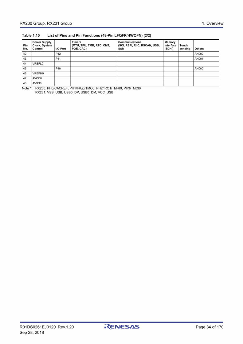
R01DS0261EJ0120 Rev.1.20 Page 34 of 170Sep 28, 2018
RX230 Group, RX231 Group 1. Overview
Note 1. RX230: PH0/CACREF, PH1/IRQ0/TMO0, PH2/IRQ1/TMRI0, PH3/TMCI0RX231: VSS_USB, USB0_DP, USB0_DM, VCC_USB
42 P42 AN002
43 P41 AN001
44 VREFL0
45 P40 AN000
46 VREFH0
47 AVCC0
48 AVSS0
Table 1.10 List of Pins and Pin Functions (48-Pin LFQFP/HWQFN) (2/2)
Pin No.
Power Supply, Clock, System Control I/O Port
Timers(MTU, TPU, TMR, RTC, CMT, POE, CAC)
Communications(SCI, RSPI, RIIC, RSCAN, USB, SSI)
Memory Interface (SDHI)
Touch sensing Others
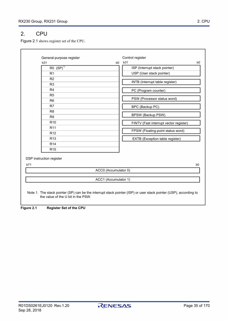
R01DS0261EJ0120 Rev.1.20 Page 35 of 170Sep 28, 2018
RX230 Group, RX231 Group 2. CPU
2. CPUFigure 2.1 shows register set of the CPU.
Figure 2.1 Register Set of the CPU
Note 1. The stack pointer (SP) can be the interrupt stack pointer (ISP) or user stack pointer (USP), according to the value of the U bit in the PSW.
R15 R14 R13 R12 R11 R10 R9 R8 R7 R6 R5 R4 R3 R2 R1 R0 (SP)*1
General-purpose registerb31 b0
DSP instruction register
b71 b0
ACC0 (Accumulator 0)
ACC1 (Accumulator 1)
USP (User stack pointer)ISP (Interrupt stack pointer)
INTB (Interrupt table register)
PC (Program counter)
PSW (Processor status word)
BPC (Backup PC)
BPSW (Backup PSW)
FINTV (Fast interrupt vector register)
FPSW (Floating-point status word)
Control registerb31 b0
EXTB (Exception table register)
R01DS0261EJ0120 Rev.1.20 Page 36 of 170Sep 28, 2018
RX230 Group, RX231 Group 2. CPU
2.1 General-Purpose Registers (R0 to R15)This CPU has sixteen 32-bit general-purpose registers (R0 to R15). R0 to R15 can be used as data registers or address registers.R0, a general-purpose register, also functions as the stack pointer (SP). The stack pointer is switched to operate as the interrupt stack pointer (ISP) or user stack pointer (USP) by the value of the stack pointer select bit (U) in the processor status word (PSW).
2.2 Control Registers
(1) Interrupt stack pointer (ISP) and user stack pointer (USP)The stack pointer (SP) can be either of two types, the interrupt stack pointer (ISP) or the user stack pointer (USP). Whether the stack pointer operates as the ISP or USP depends on the value of the stack pointer select bit (U) in the processor status word (PSW).Set the ISP or USP to a multiple of 4 to reduce the number of cycles required to execute interrupt sequences and instructions entailing stack manipulation.
(2) Exception table register (EXTB)The exception table register (EXTB) specifies the address where the exception vector table starts.Set the EXTB to a multiple of 4 to reduce the number of cycles required to execute interrupt sequences and instructions entailing stack manipulation.
(3) Interrupt table register (INTB)The interrupt table register (INTB) specifies the address where the interrupt vector table starts.Set the INTB to a multiple of 4 to reduce the number of cycles required to execute interrupt sequences and instructions entailing stack manipulation.
(4) Program counter (PC)The program counter (PC) indicates the address of the instruction being executed.
(5) Processor status word (PSW)The processor status word (PSW) indicates the results of instruction execution or the state of the CPU.
(6) Backup PC (BPC)The backup PC (BPC) is provided to speed up response to interrupts.After a fast interrupt has been generated, the contents of the program counter (PC) are saved in the BPC register.
(7) Backup PSW (BPSW)The backup PSW (BPSW) is provided to speed up response to interrupts. After a fast interrupt has been generated, the contents of the processor status word (PSW) are saved in the BPSW. The allocation of bits in the BPSW corresponds to that in the PSW.
(8) Fast interrupt vector register (FINTV)The fast interrupt vector register (FINTV) is provided to speed up response to interrupts.The FINTV register specifies a branch destination address when a fast interrupt has been generated.
R01DS0261EJ0120 Rev.1.20 Page 37 of 170Sep 28, 2018
RX230 Group, RX231 Group 2. CPU
(9) Floating-point status word (FPSW)The floating-point status word (FPSW) indicates the results of floating-point operations.When an exception handling enable bit (Ej) enables the exception handling (Ej = 1), the exception cause can be identified by checking the corresponding Cj flag in the exception handling routine. If the exception handling is masked (Ej = 0), the occurrence of exception can be checked by reading the Fj flag at the end of a series of processing. Once the Fj flag has been set to 1, this value is retained until it is cleared to 0 by software (j = X, U, Z, O, or V).
2.3 AccumulatorThe accumulator (ACC0 or ACC1) is a 72-bit register used for DSP instructions. The accumulator is handled as a 96-bit register for reading and writing. At this time, when bits 95 to 72 of the accumulator are read, the value where the value of bit 71 is sign extended is read. Writing to bits 95 to 72 of the accumulator is ignored. ACC0 is also used for the multiply and multiply-and-accumulate instructions; EMUL, EMULU, FMUL, MUL, and RMPA, in which case the prior value in ACC0 is modified by execution of the instruction.Use the MVTACGU, MVTACHI, and MVTACLO instructions for writing to the accumulator. The MVTACGU, MVTACHI, and MVTACLO instructions write data to bits 95 to 64, the higher-order 32 bits (bits 63 to 32), and the lower-order 32 bits (bits 31 to 0), respectively.Use the MVFACGU, MVFACHI, MVFACMI, and MVFACLO instructions for reading data from the accumulator. The MVFACGU, MVFACHI, MVFACMI, and MVFACLO instructions read data from the guard bits (bits 95 to 64), higher-order 32 bits (bits 63 to 32), the middle 32 bits (bits 47 to 16), and the lower-order 32 bits (bits 31 to 0), respectively.

R01DS0261EJ0120 Rev.1.20 Page 38 of 170Sep 28, 2018
RX230 Group, RX231 Group 3. Address Space
3. Address Space
3.1 Address SpaceThis LSI has a 4-Gbyte address space, consisting of the range of addresses from 0000 0000h to FFFF FFFFh. That is, linear access to an address space of up to 4 Gbytes is possible, and this contains both program and data areas.Figure 3.1 shows the memory maps in the respective operating modes. Accessible areas will differ according to the operating mode and states of control bits.

R01DS0261EJ0120 Rev.1.20 Page 39 of 170Sep 28, 2018
RX230 Group, RX231 Group 3. Address Space
Figure 3.1 Memory Map in Each Operating Mode
Reserved area*3Reserved area*3
Reserved area*3Reserved area*3
Reserved area*3
Reserved area*3
Reserved area*3
Reserved area*3
Reserved area*3
Reserved area*3
Reserved area*3
External address space(CS area)
External address space(CS area)
On-chip ROM (E2DataFlash)
Reserved area*3
0000 0000h
0008 0000h
FFFF FFFFh
Single-chip mode*1
RAM*2
On-chip ROM (program ROM)(read only)*2
0010 0000h
Peripheral I/O registers
0010 2000h
0080 0000h
FFF8 0000h
Peripheral I/O registers
Peripheral I/O registers
007F C000h007F C500h
007F FC00h
0001 0000h0000 0000h
0008 0000h
FFFF FFFFh
On-chip ROM enabled extended mode
RAM*2
On-chip ROM (program ROM)(read only)*2
0010 0000h
Peripheral I/O registers
0010 2000h
On-chip ROM (E2DataFlash)
0080 0000h
0500 0000h
0800 0000h
FFF8 0000h
Peripheral I/O registers
Peripheral I/O registers
007F C000h007F C500h
007F FC00h
0001 0000h
0000 0000h
0008 0000h
FFFF FFFFh
On-chip ROM disabled extended mode
RAM*2
0010 0000h
Peripheral I/O registers
0500 0000h
0800 0000h
FF00 0000h
0001 0000h
External address space
Note 1. The address space in boot mode and USB boot mode is the same as the address space in single-chip mode.Note 2. The capacity of ROM/RAM differs depending on the products.
Note: See Table 1.3 and Table 1.4 List of Products, for the product type name.
Note 3. Reserved areas should not be accessed.
ROM (bytes) RAM (bytes)
Capacity Address Capacity Address
512 Kbytes FFF8 0000h to FFFF FFFFh 64 Kbytes 0000 0000h to 0000 FFFFh
384 Kbytes FFFA 0000h to FFFF FFFFh
256 Kbytes FFFC 0000h to FFFF FFFFh 32 Kbytes 0000 0000h to 0000 7FFFh
128 Kbytes FFFE 0000h to FFFF FFFFh

R01DS0261EJ0120 Rev.1.20 Page 40 of 170Sep 28, 2018
RX230 Group, RX231 Group 3. Address Space
3.2 External Address SpaceThe external address space is divided into up to four CS areas (CS0 to CS3), each corresponding to the CSn# signal output from a CSn# (n = 0 to 3) pin. Figure 3.2 shows the address ranges corresponding to the individual CS areas (CS0 to CS3) in on-chip ROM disabled extended mode.
Figure 3.2 Correspondence between External Address Spaces and CS Areas(In On-Chip ROM Disabled Extended Mode)
Reserved area*1
Reserved area*1
Reserved area*1
0000 0000h
0008 0000h
RAM
External address space(CS area)
0010 0000h
Peripheral I/O registers
0500 0000h
0800 0000h
FF00 0000h
0001 0000h
External address space*2
(CS area)
0500 0000h
0600 0000h
0700 0000h
05FF FFFFh
06FF FFFFh
07FF FFFFh
CS3 (16 Mbytes)
CS2 (16 Mbytes)
CS1 (16 Mbytes)
FFFF FFFFh FFFF FFFFh
FF00 0000h
CS0 (16 Mbytes)
Note 1. Reserved areas should not be accessed.Note 2. The CS0 area is disabled in on-chip ROM enabled extended mode.
In this mode, the address space for addresses above 1000 0000h is as shown in figure on this section, Memory Map in Each Operating Mode.

R01DS0261EJ0120 Rev.1.20 Page 41 of 170Sep 28, 2018
RX230 Group, RX231 Group 4. I/O Registers
4. I/O RegistersThis section provides information on the on-chip I/O register addresses and bit configuration. The information is given as shown below. Notes on writing to registers are also given below.
(1) I/O register addresses (address order)• Registers are listed from the lower allocation addresses.• Registers are classified according to module symbols.• Numbers of cycles for access indicate numbers of cycles of the given base clock.• Among the internal I/O register area, addresses not listed in the list of registers are reserved. Reserved addresses
must not be accessed. Do not access these addresses; otherwise, the operation when accessing these bits and subsequent operations cannot be guaranteed.
(2) Notes on writing to I/O registersWhen writing to an I/O register, the CPU starts executing the subsequent instruction before completing I/O register write. This may cause the subsequent instruction to be executed before the post-update I/O register value is reflected on the operation.As described in the following examples, special care is required for the cases in which the subsequent instruction must be executed after the post-update I/O register value is actually reflected.
[Examples of cases requiring special care]• The subsequent instruction must be executed while an interrupt request is disabled with the IENj bit in IERn of the
ICU (interrupt request enable bit) cleared to 0.• A WAIT instruction is executed immediately after the preprocessing for causing a transition to the low power
consumption state.
In the above cases, after writing to an I/O register, wait until the write operation is completed using the following procedure and then execute the subsequent instruction.
(a) Write to an I/O register.(b) Read the value from the I/O register to a general register.(c) Execute the operation using the value read.(d) Execute the subsequent instruction.
[Instruction examples]• Byte-size I/O registers
MOV.L #SFR_ADDR, R1 MOV.B #SFR_DATA, [R1] CMP [R1].UB, R1 ;; Next process
• Word-size I/O registers
MOV.L #SFR_ADDR, R1 MOV.W #SFR_DATA, [R1] CMP [R1].W, R1 ;; Next process

R01DS0261EJ0120 Rev.1.20 Page 42 of 170Sep 28, 2018
RX230 Group, RX231 Group 4. I/O Registers
• Longword-size I/O registers
MOV.L #SFR_ADDR, R1 MOV.L #SFR_DATA, [R1] CMP [R1].L, R1 ;; Next process
If multiple registers are written to and a subsequent instruction should be executed after the write operations are entirely completed, only read the I/O register that was last written to and execute the operation using the value; it is not necessary to read or execute operation for all the registers that were written to.
(3) Number of Access Cycles to I/O RegistersFor numbers of clock cycles for access to I/O registers, see Table 4.1, List of I/O Registers (Address Order).The number of access cycles to I/O registers is obtained by following equation.*1
Number of access cycles to I/O registers = Number of bus cycles for internal main bus 1 +Number of divided clock synchronization cycles +Number of bus cycles for internal peripheral bus 1 to 6
The number of bus cycles of internal peripheral bus 1 to 6 differs according to the register to be accessed.When peripheral functions connected to internal peripheral bus 2 to 6 or registers for the external bus control unit (except for bus error related registers) are accessed, the number of divided clock synchronization cycles is added.The number of divided clock synchronization cycles differs depending on the frequency ratio between ICLK and PCLK (or FCLK, BCLK) or bus access timing.In the peripheral function unit, when the frequency ratio of ICLK is equal to or greater than that of PCLK (or FCLK), the sum of the number of bus cycles for internal main bus 1 and the number of the divided clock synchronization cycles will be one cycle of PCLK (or FCLK) at a maximum. Therefore, one PCLK (or FCLK) has been added to the number of access cycles shown in Table 4.1.When the frequency ratio of ICLK is lower than that of PCLK (or FCLK), the subsequent bus access is started from the ICLK cycle following the completion of the access to the peripheral functions. Therefore, the access cycles are described on an ICLK basis.In the external bus control unit, the sum of the number of bus cycles for internal main bus 1 and the number of divided clock synchronization cycles will be one cycle of BCLK at a maximum. Therefore, one BCLK is added to the number of access cycles shown in Table 4.1.
Note 1. This applies to the number of cycles when the access from the CPU does not conflict with the instruction fetching to the external memory or bus access from the different bus master (DMAC or DTC).
(4) Restrictions in Relation to RMPA and String-Manipulation InstructionsThe allocation of data to be handled by RMPA or string-manipulation instructions to I/O registers is prohibited, and operation is not guaranteed if this restriction is not observed.
(5) Notes on Sleep Mode and Mode TransitionsDuring sleep mode or mode transitions, do not write to the system control related registers (indicated by 'SYSTEM' in the Module Symbol column in Table 4.1, List of I/O Registers (Address Order)).
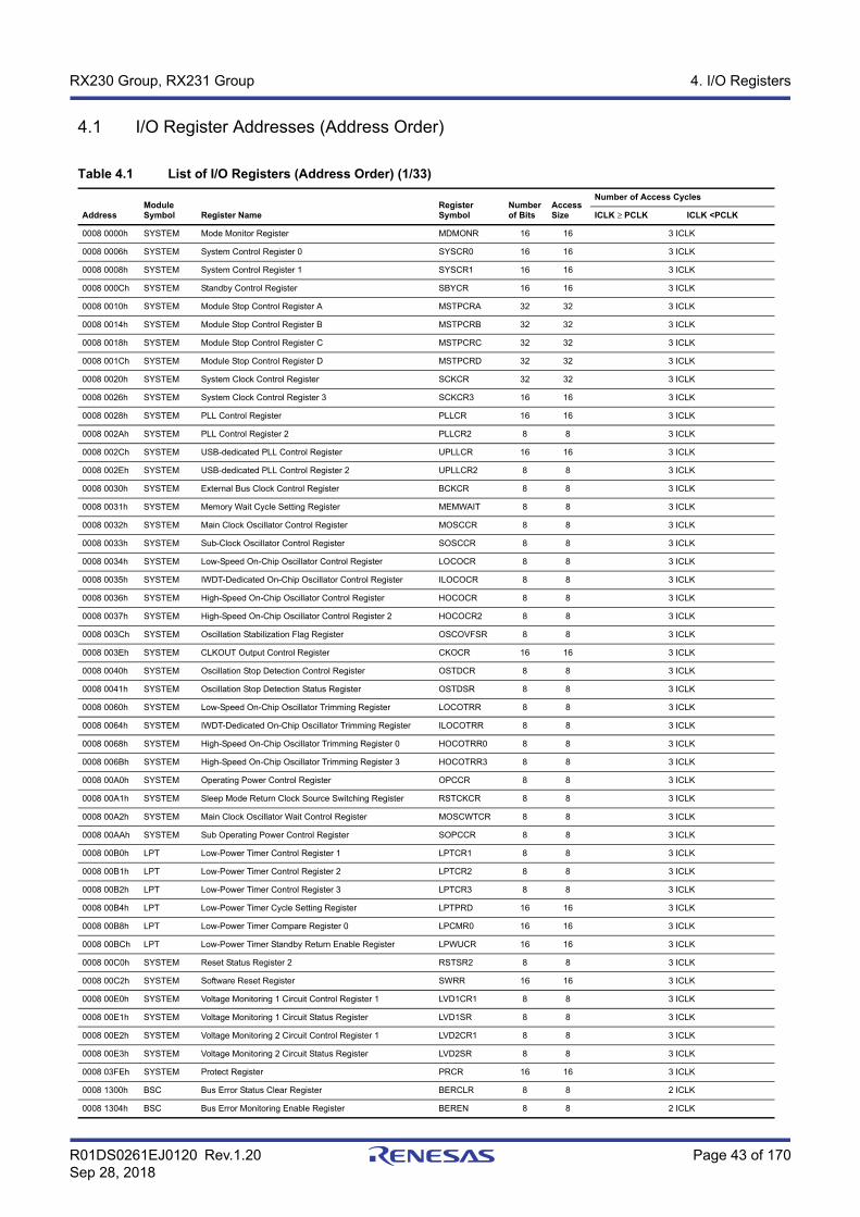
R01DS0261EJ0120 Rev.1.20 Page 43 of 170Sep 28, 2018
RX230 Group, RX231 Group 4. I/O Registers
4.1 I/O Register Addresses (Address Order)
Table 4.1 List of I/O Registers (Address Order) (1/33)
AddressModule Symbol Register Name
Register Symbol
Number of Bits
Access Size
Number of Access Cycles
ICLK ≥ PCLK ICLK <PCLK
0008 0000h SYSTEM Mode Monitor Register MDMONR 16 16 3 ICLK
0008 0006h SYSTEM System Control Register 0 SYSCR0 16 16 3 ICLK
0008 0008h SYSTEM System Control Register 1 SYSCR1 16 16 3 ICLK
0008 000Ch SYSTEM Standby Control Register SBYCR 16 16 3 ICLK
0008 0010h SYSTEM Module Stop Control Register A MSTPCRA 32 32 3 ICLK
0008 0014h SYSTEM Module Stop Control Register B MSTPCRB 32 32 3 ICLK
0008 0018h SYSTEM Module Stop Control Register C MSTPCRC 32 32 3 ICLK
0008 001Ch SYSTEM Module Stop Control Register D MSTPCRD 32 32 3 ICLK
0008 0020h SYSTEM System Clock Control Register SCKCR 32 32 3 ICLK
0008 0026h SYSTEM System Clock Control Register 3 SCKCR3 16 16 3 ICLK
0008 0028h SYSTEM PLL Control Register PLLCR 16 16 3 ICLK
0008 002Ah SYSTEM PLL Control Register 2 PLLCR2 8 8 3 ICLK
0008 002Ch SYSTEM USB-dedicated PLL Control Register UPLLCR 16 16 3 ICLK
0008 002Eh SYSTEM USB-dedicated PLL Control Register 2 UPLLCR2 8 8 3 ICLK
0008 0030h SYSTEM External Bus Clock Control Register BCKCR 8 8 3 ICLK
0008 0031h SYSTEM Memory Wait Cycle Setting Register MEMWAIT 8 8 3 ICLK
0008 0032h SYSTEM Main Clock Oscillator Control Register MOSCCR 8 8 3 ICLK
0008 0033h SYSTEM Sub-Clock Oscillator Control Register SOSCCR 8 8 3 ICLK
0008 0034h SYSTEM Low-Speed On-Chip Oscillator Control Register LOCOCR 8 8 3 ICLK
0008 0035h SYSTEM IWDT-Dedicated On-Chip Oscillator Control Register ILOCOCR 8 8 3 ICLK
0008 0036h SYSTEM High-Speed On-Chip Oscillator Control Register HOCOCR 8 8 3 ICLK
0008 0037h SYSTEM High-Speed On-Chip Oscillator Control Register 2 HOCOCR2 8 8 3 ICLK
0008 003Ch SYSTEM Oscillation Stabilization Flag Register OSCOVFSR 8 8 3 ICLK
0008 003Eh SYSTEM CLKOUT Output Control Register CKOCR 16 16 3 ICLK
0008 0040h SYSTEM Oscillation Stop Detection Control Register OSTDCR 8 8 3 ICLK
0008 0041h SYSTEM Oscillation Stop Detection Status Register OSTDSR 8 8 3 ICLK
0008 0060h SYSTEM Low-Speed On-Chip Oscillator Trimming Register LOCOTRR 8 8 3 ICLK
0008 0064h SYSTEM IWDT-Dedicated On-Chip Oscillator Trimming Register ILOCOTRR 8 8 3 ICLK
0008 0068h SYSTEM High-Speed On-Chip Oscillator Trimming Register 0 HOCOTRR0 8 8 3 ICLK
0008 006Bh SYSTEM High-Speed On-Chip Oscillator Trimming Register 3 HOCOTRR3 8 8 3 ICLK
0008 00A0h SYSTEM Operating Power Control Register OPCCR 8 8 3 ICLK
0008 00A1h SYSTEM Sleep Mode Return Clock Source Switching Register RSTCKCR 8 8 3 ICLK
0008 00A2h SYSTEM Main Clock Oscillator Wait Control Register MOSCWTCR 8 8 3 ICLK
0008 00AAh SYSTEM Sub Operating Power Control Register SOPCCR 8 8 3 ICLK
0008 00B0h LPT Low-Power Timer Control Register 1 LPTCR1 8 8 3 ICLK
0008 00B1h LPT Low-Power Timer Control Register 2 LPTCR2 8 8 3 ICLK
0008 00B2h LPT Low-Power Timer Control Register 3 LPTCR3 8 8 3 ICLK
0008 00B4h LPT Low-Power Timer Cycle Setting Register LPTPRD 16 16 3 ICLK
0008 00B8h LPT Low-Power Timer Compare Register 0 LPCMR0 16 16 3 ICLK
0008 00BCh LPT Low-Power Timer Standby Return Enable Register LPWUCR 16 16 3 ICLK
0008 00C0h SYSTEM Reset Status Register 2 RSTSR2 8 8 3 ICLK
0008 00C2h SYSTEM Software Reset Register SWRR 16 16 3 ICLK
0008 00E0h SYSTEM Voltage Monitoring 1 Circuit Control Register 1 LVD1CR1 8 8 3 ICLK
0008 00E1h SYSTEM Voltage Monitoring 1 Circuit Status Register LVD1SR 8 8 3 ICLK
0008 00E2h SYSTEM Voltage Monitoring 2 Circuit Control Register 1 LVD2CR1 8 8 3 ICLK
0008 00E3h SYSTEM Voltage Monitoring 2 Circuit Status Register LVD2SR 8 8 3 ICLK
0008 03FEh SYSTEM Protect Register PRCR 16 16 3 ICLK
0008 1300h BSC Bus Error Status Clear Register BERCLR 8 8 2 ICLK
0008 1304h BSC Bus Error Monitoring Enable Register BEREN 8 8 2 ICLK

R01DS0261EJ0120 Rev.1.20 Page 44 of 170Sep 28, 2018
RX230 Group, RX231 Group 4. I/O Registers
0008 1308h BSC Bus Error Status Register 1 BERSR1 8 8 2 ICLK
0008 130Ah BSC Bus Error Status Register 2 BERSR2 16 16 2 ICLK
0008 1310h BSC Bus Priority Control Register BUSPRI 16 16 2 ICLK
0008 2000h DMAC0 DMA Source Address Register DMSAR 32 32 2 ICLK
0008 2004h DMAC0 DMA Destination Address Register DMDAR 32 32 2 ICLK
0008 2008h DMAC0 DMA Transfer Count Register DMCRA 32 32 2 ICLK
0008 200Ch DMAC0 DMA Block Transfer Count Register DMCRB 16 16 2 ICLK
0008 2010h DMAC0 DMA Transfer Mode Register DMTMD 16 16 2 ICLK
0008 2013h DMAC0 DMA Interrupt Setting Register DMINT 8 8 2 ICLK
0008 2014h DMAC0 DMA Address Mode Register DMAMD 16 16 2 ICLK
0008 2018h DMAC0 DMA Offset Register DMOFR 32 32 2 ICLK
0008 201Ch DMAC0 DMA Transfer Enable Register DMCNT 8 8 2 ICLK
0008 201Dh DMAC0 DMA Software Start Register DMREQ 8 8 2 ICLK
0008 201Eh DMAC0 DMA Status Register DMSTS 8 8 2 ICLK
0008 201Fh DMAC0 DMA Activation Source Flag Control Register DMCSL 8 8 2 ICLK
0008 2040h DMAC1 DMA Source Address Register DMSAR 32 32 2 ICLK
0008 2044h DMAC1 DMA Destination Address Register DMDAR 32 32 2 ICLK
0008 2048h DMAC1 DMA Transfer Count Register DMCRA 32 32 2 ICLK
0008 204Ch DMAC1 DMA Block Transfer Count Register DMCRB 16 16 2 ICLK
0008 2050h DMAC1 DMA Transfer Mode Register DMTMD 16 16 2 ICLK
0008 2053h DMAC1 DMA Interrupt Setting Register DMINT 8 8 2 ICLK
0008 2054h DMAC1 DMA Address Mode Register DMAMD 16 16 2 ICLK
0008 205Ch DMAC1 DMA Transfer Enable Register DMCNT 8 8 2 ICLK
0008 205Dh DMAC1 DMA Software Start Register DMREQ 8 8 2 ICLK
0008 205Eh DMAC1 DMA Status Register DMSTS 8 8 2 ICLK
0008 205Fh DMAC1 DMA Activation Source Flag Control Register DMCSL 8 8 2 ICLK
0008 2080h DMAC2 DMA Source Address Register DMSAR 32 32 2 ICLK
0008 2084h DMAC2 DMA Destination Address Register DMDAR 32 32 2 ICLK
0008 2088h DMAC2 DMA Transfer Count Register DMCRA 32 32 2 ICLK
0008 208Ch DMAC2 DMA Block Transfer Count Register DMCRB 16 16 2 ICLK
0008 2090h DMAC2 DMA Transfer Mode Register DMTMD 16 16 2 ICLK
0008 2093h DMAC2 DMA Interrupt Setting Register DMINT 8 8 2 ICLK
0008 2094h DMAC2 DMA Address Mode Register DMAMD 16 16 2 ICLK
0008 209Ch DMAC2 DMA Transfer Enable Register DMCNT 8 8 2 ICLK
0008 209Dh DMAC2 DMA Software Start Register DMREQ 8 8 2 ICLK
0008 209Eh DMAC2 DMA Status Register DMSTS 8 8 2 ICLK
0008 209Fh DMAC2 DMA Activation Source Flag Control Register DMCSL 8 8 2 ICLK
0008 20C0h DMAC3 DMA Source Address Register DMSAR 32 32 2 ICLK
0008 20C4h DMAC3 DMA Destination Address Register DMDAR 32 32 2 ICLK
0008 20C8h DMAC3 DMA Transfer Count Register DMCRA 32 32 2 ICLK
0008 20CCh DMAC3 DMA Block Transfer Count Register DMCRB 16 16 2 ICLK
0008 20D0h DMAC3 DMA Transfer Mode Register DMTMD 16 16 2 ICLK
0008 20D3h DMAC3 DMA Interrupt Setting Register DMINT 8 8 2 ICLK
0008 20D4h DMAC3 DMA Address Mode Register DMAMD 16 16 2 ICLK
0008 20DCh DMAC3 DMA Transfer Enable Register DMCNT 8 8 2 ICLK
0008 20DDh DMAC3 DMA Software Start Register DMREQ 8 8 2 ICLK
0008 20DEh DMAC3 DMA Status Register DMSTS 8 8 2 ICLK
0008 20DFh DMAC3 DMA Activation Source Flag Control Register DMCSL 8 8 2 ICLK
0008 2200h DMAC DMA Module Activation Register DMAST 8 8 2 ICLK
0008 2400h DTC DTC Control Register DTCCR 8 8 2 ICLK
0008 2404h DTC DTC Vector Base Register DTCVBR 32 32 2 ICLK
0008 2408h DTC DTC Address Mode Register DTCADMOD 8 8 2 ICLK
Table 4.1 List of I/O Registers (Address Order) (2/33)
AddressModule Symbol Register Name
Register Symbol
Number of Bits
Access Size
Number of Access Cycles
ICLK ≥ PCLK ICLK <PCLK
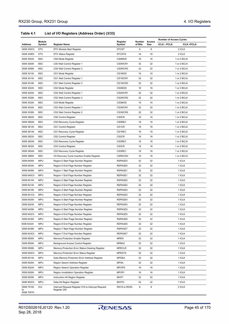
R01DS0261EJ0120 Rev.1.20 Page 45 of 170Sep 28, 2018
RX230 Group, RX231 Group 4. I/O Registers
0008 240Ch DTC DTC Module Start Register DTCST 8 8 2 ICLK
0008 240Eh DTC DTC Status Register DTCSTS 16 16 2 ICLK
0008 3002h BSC CS0 Mode Register CS0MOD 16 16 1 or 2 BCLK
0008 3004h BSC CS0 Wait Control Register 1 CS0WCR1 32 32 1 or 2 BCLK
0008 3008h BSC CS0 Wait Control Register 2 CS0WCR2 32 32 1 or 2 BCLK
0008 3012h BSC CS1 Mode Register CS1MOD 16 16 1 or 2 BCLK
0008 3014h BSC CS1 Wait Control Register 1 CS1WCR1 32 32 1 or 2 BCLK
0008 3018h BSC CS1 Wait Control Register 2 CS1WCR2 32 32 1 or 2 BCLK
0008 3022h BSC CS2 Mode Register CS2MOD 16 16 1 or 2 BCLK
0008 3024h BSC CS2 Wait Control Register 1 CS2WCR1 32 32 1 or 2 BCLK
0008 3028h BSC CS2 Wait Control Register 2 CS2WCR2 32 32 1 or 2 BCLK
0008 3032h BSC CS3 Mode Register CS3MOD 16 16 1 or 2 BCLK
0008 3034h BSC CS3 Wait Control Register 1 CS3WCR1 32 32 1 or 2 BCLK
0008 3038h BSC CS3 Wait Control Register 2 CS3WCR2 32 32 1 or 2 BCLK
0008 3802h BSC CS0 Control Register CS0CR 16 16 1 or 2 BCLK
0008 380Ah BSC CS0 Recovery Cycle Register CS0REC 16 16 1 or 2 BCLK
0008 3812h BSC CS1 Control Register CS1CR 16 16 1 or 2 BCLK
0008 381Ah BSC CS1 Recovery Cycle Register CS1REC 16 16 1 or 2 BCLK
0008 3822h BSC CS2 Control Register CS2CR 16 16 1 or 2 BCLK
0008 382Ah BSC CS2 Recovery Cycle Register CS2REC 16 16 1 or 2 BCLK
0008 3832h BSC CS3 Control Register CS3CR 16 16 1 or 2 BCLK
0008 383Ah BSC CS3 Recovery Cycle Register CS3REC 16 16 1 or 2 BCLK
0008 3880h BSC CS Recovery Cycle Insertion Enable Register CSRECEN 16 16 1 or 2 BCLK
0008 6400h MPU Region-0 Start Page Number Register RSPAGE0 32 32 1 ICLK
0008 6404h MPU Region-0 End Page Number Register REPAGE0 32 32 1 ICLK
0008 6408h MPU Region-1 Start Page Number Register RSPAGE1 32 32 1 ICLK
0008 640Ch MPU Region-1 End Page Number Register REPAGE1 32 32 1 ICLK
0008 6410h MPU Region-2 Start Page Number Register RSPAGE2 32 32 1 ICLK
0008 6414h MPU Region-2 End Page Number Register REPAGE2 32 32 1 ICLK
0008 6418h MPU Region-3 Start Page Number Register RSPAGE3 32 32 1 ICLK
0008 641Ch MPU Region-3 End Page Number Register REPAGE3 32 32 1 ICLK
0008 6420h MPU Region-4 Start Page Number Register RSPAGE4 32 32 1 ICLK
0008 6424h MPU Region-4 End Page Number Register REPAGE4 32 32 1 ICLK
0008 6428h MPU Region-5 Start Page Number Register RSPAGE5 32 32 1 ICLK
0008 642Ch MPU Region-5 End Page Number Register REPAGE5 32 32 1 ICLK
0008 6430h MPU Region-6 Start Page Number Register RSPAGE6 32 32 1 ICLK
0008 6434h MPU Region-6 End Page Number Register REPAGE6 32 32 1 ICLK
0008 6438h MPU Region-7 Start Page Number Register RSPAGE7 32 32 1 ICLK
0008 643Ch MPU Region-7 End Page Number Register REPAGE7 32 32 1 ICLK
0008 6500h MPU Memory-Protection Enable Register MPEN 32 32 1 ICLK
0008 6504h MPU Background Access Control Register MPBAC 32 32 1 ICLK
0008 6508h MPU Memory-Protection Error Status-Clearing Register MPECLR 32 32 1 ICLK
0008 650Ch MPU Memory-Protection Error Status Register MPESTS 32 32 1 ICLK
0008 6514h MPU Data Memory-Protection Error Address Register MPDEA 32 32 1 ICLK
0008 6520h MPU Region Search Address Register MPSA 32 32 1 ICLK
0008 6524h MPU Region Search Operation Register MPOPS 16 16 1 ICLK
0008 6526h MPU Region Invalidation Operation Register MPOPI 16 16 1 ICLK
0008 6528h MPU Instruction-Hit Region Register MHITI 32 32 1 ICLK
0008 652Ch MPU Data-Hit Region Register MHITD 32 32 1 ICLK
0008 7010h to 0008 70FFh
ICU Interrupt Request Register 016 to Interrupt Request Register 255
IR016 to IR255 8 8 2 ICLK
Table 4.1 List of I/O Registers (Address Order) (3/33)
AddressModule Symbol Register Name
Register Symbol
Number of Bits
Access Size
Number of Access Cycles
ICLK ≥ PCLK ICLK <PCLK

R01DS0261EJ0120 Rev.1.20 Page 46 of 170Sep 28, 2018
RX230 Group, RX231 Group 4. I/O Registers
0008 711Bh to 0008 71FFh
ICU DTC Activation Enable Register 027 to DTC Activation Enable Register 255
DTCER027 to DTCER255
8 8 2 ICLK
0008 7202h to 0008 721Fh
ICU Interrupt Request Enable Register 02 to Interrupt Request Enable Register 1F
IER02 to IER1F 8 8 2 ICLK
0008 72E0h ICU Software Interrupt Generation Register SWINTR 8 8 2 ICLK
0008 72F0h ICU Fast Interrupt Set Register FIR 16 16 2 ICLK
0008 7300h to 0008 73FFh
ICU Interrupt Source Priority Register 000 to Interrupt Source Priority Register 255
IPR000 to IPR255
8 8 2 ICLK
0008 7400h ICU DMAC Activation Request Select Register 0 DMRSR0 8 8 2 ICLK
0008 7404h ICU DMAC Activation Request Select Register 1 DMRSR1 8 8 2 ICLK
0008 7408h ICU DMAC Activation Request Select Register 2 DMRSR2 8 8 2 ICLK
0008 740Ch ICU DMAC Activation Request Select Register 3 DMRSR3 8 8 2 ICLK
0008 7500h to 0008 7507h
ICU IRQ Control Register 0 to IRQ Control Register 7 IRQCR0 to IRQCR7
8 8 2 ICLK
0008 7510h ICU IRQ Pin Digital Filter Enable Register 0 IRQFLTE0 8 8 2 ICLK
0008 7514h ICU IRQ Pin Digital Filter Setting Register 0 IRQFLTC0 16 16 2 ICLK
0008 7580h ICU Non-Maskable Interrupt Status Register NMISR 8 8 2 ICLK
0008 7581h ICU Non-Maskable Interrupt Enable Register NMIER 8 8 2 ICLK
0008 7582h ICU Non-Maskable Interrupt Status Clear Register NMICLR 8 8 2 ICLK
0008 7583h ICU NMI Pin Interrupt Control Register NMICR 8 8 2 ICLK
0008 7590h ICU NMI Pin Digital Filter Enable Register NMIFLTE 8 8 2 ICLK
0008 7594h ICU NMI Pin Digital Filter Setting Register NMIFLTC 8 8 2 ICLK
0008 8000h CMT Compare Match Timer Start Register 0 CMSTR0 16 16 2 or 3 PCLKB 2 ICLK
0008 8002h CMT0 Compare Match Timer Control Register CMCR 16 16 2 or 3 PCLKB 2 ICLK
0008 8004h CMT0 Compare Match Counter CMCNT 16 16 2 or 3 PCLKB 2 ICLK
0008 8006h CMT0 Compare Match Constant Register CMCOR 16 16 2 or 3 PCLKB 2 ICLK
0008 8008h CMT1 Compare Match Timer Control Register CMCR 16 16 2 or 3 PCLKB 2 ICLK
0008 800Ah CMT1 Compare Match Counter CMCNT 16 16 2 or 3 PCLKB 2 ICLK
0008 800Ch CMT1 Compare Match Constant Register CMCOR 16 16 2 or 3 PCLKB 2 ICLK
0008 8010h CMT Compare Match Timer Start Register 1 CMSTR1 16 16 2 or 3 PCLKB 2 ICLK
0008 8012h CMT2 Compare Match Timer Control Register CMCR 16 16 2 or 3 PCLKB 2 ICLK
0008 8014h CMT2 Compare Match Counter CMCNT 16 16 2 or 3 PCLKB 2 ICLK
0008 8016h CMT2 Compare Match Constant Register CMCOR 16 16 2 or 3 PCLKB 2 ICLK
0008 8018h CMT3 Compare Match Timer Control Register CMCR 16 16 2 or 3 PCLKB 2 ICLK
0008 801Ah CMT3 Compare Match Counter CMCNT 16 16 2 or 3 PCLKB 2 ICLK
0008 801Ch CMT3 Compare Match Constant Register CMCOR 16 16 2 or 3 PCLKB 2 ICLK
0008 8020h WDT WDT Refresh Register WDTRR 8 8 2 or 3 PCLKB 2 ICLK
0008 8022h WDT WDT Control Register WDTCR 16 16 2 or 3 PCLKB 2 ICLK
0008 8024h WDT WDT Status Register WDTSR 16 16 2 or 3 PCLKB 2 ICLK
0008 8026h WDT WDT Reset Control Register WDTRCR 8 8 2 or 3 PCLKB 2 ICLK
0008 8030h IWDT IWDT Refresh Register IWDTRR 8 8 2 or 3 PCLKB 2 ICLK
0008 8032h IWDT IWDT Control Register IWDTCR 16 16 2 or 3 PCLKB 2 ICLK
0008 8034h IWDT IWDT Status Register IWDTSR 16 16 2 or 3 PCLKB 2 ICLK
0008 8036h IWDT IWDT Reset Control Register IWDTRCR 8 8 2 or 3 PCLKB 2 ICLK
0008 8038h IWDT IWDT Count Stop Control Register IWDTCSTPR 8 8 2 or 3 PCLKB 2 ICLK
0008 8040h DA D/A Data Register 0 DADR0 16 16 2 or 3 PCLKB 2 ICLK
0008 8042h DA D/A Data Register 1 DADR1 16 16 2 or 3 PCLKB 2 ICLK
0008 8044h DA D/A Control Register DACR 8 8 2 or 3 PCLKB 2 ICLK
0008 8045h DA DADRm Format Select Register DADPR 8 8 2 or 3 PCLKB 2 ICLK
0008 8046h DA D/A A/D Synchronous Start Control Register DAADSCR 8 8 2 or 3 PCLKB 2 ICLK
0008 8047h DA D/A VREF Control Register DAVREFCR 8 8 2 or 3 PCLKB 2 ICLK
Table 4.1 List of I/O Registers (Address Order) (4/33)
AddressModule Symbol Register Name
Register Symbol
Number of Bits
Access Size
Number of Access Cycles
ICLK ≥ PCLK ICLK <PCLK
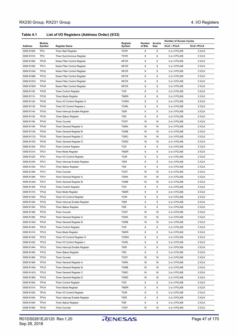
R01DS0261EJ0120 Rev.1.20 Page 47 of 170Sep 28, 2018
RX230 Group, RX231 Group 4. I/O Registers
0008 8100h TPU Timer Start Register TSTR 8 8 2 or 3 PCLKB 2 ICLK
0008 8101h TPU Timer Synchronous Register TSYR 8 8 2 or 3 PCLKB 2 ICLK
0008 8108h TPU0 Noise Filter Control Register NFCR 8 8 2 or 3 PCLKB 2 ICLK
0008 8109h TPU1 Noise Filter Control Register NFCR 8 8 2 or 3 PCLKB 2 ICLK
0008 810Ah TPU2 Noise Filter Control Register NFCR 8 8 2 or 3 PCLKB 2 ICLK
0008 810Bh TPU3 Noise Filter Control Register NFCR 8 8 2 or 3 PCLKB 2 ICLK
0008 810Ch TPU4 Noise Filter Control Register NFCR 8 8 2 or 3 PCLKB 2 ICLK
0008 810Dh TPU5 Noise Filter Control Register NFCR 8 8 2 or 3 PCLKB 2 ICLK
0008 8110h TPU0 Timer Control Register TCR 8 8 2 or 3 PCLKB 2 ICLK
0008 8111h TPU0 Timer Mode Register TMDR 8 8 2 or 3 PCLKB 2 ICLK
0008 8112h TPU0 Timer I/O Control Register H TIORH 8 8 2 or 3 PCLKB 2 ICLK
0008 8113h TPU0 Timer I/O Control Register L TIORL 8 8 2 or 3 PCLKB 2 ICLK
0008 8114h TPU0 Timer Interrupt Enable Register TIER 8 8 2 or 3 PCLKB 2 ICLK
0008 8115h TPU0 Timer Status Register TSR 8 8 2 or 3 PCLKB 2 ICLK
0008 8116h TPU0 Timer Counter TCNT 16 16 2 or 3 PCLKB 2 ICLK
0008 8118h TPU0 Timer General Register A TGRA 16 16 2 or 3 PCLKB 2 ICLK
0008 811Ah TPU0 Timer General Register B TGRB 16 16 2 or 3 PCLKB 2 ICLK
0008 811Ch TPU0 Timer General Register C TGRC 16 16 2 or 3 PCLKB 2 ICLK
0008 811Eh TPU0 Timer General Register D TGRD 16 16 2 or 3 PCLKB 2 ICLK
0008 8120h TPU1 Timer Control Register TCR 8 8 2 or 3 PCLKB 2 ICLK
0008 8121h TPU1 Timer Mode Register TMDR 8 8 2 or 3 PCLKB 2 ICLK
0008 8122h TPU1 Timer I/O Control Register TIOR 8 8 2 or 3 PCLKB 2 ICLK
0008 8124h TPU1 Timer Interrupt Enable Register TIER 8 8 2 or 3 PCLKB 2 ICLK
0008 8125h TPU1 Timer Status Register TSR 8 8 2 or 3 PCLKB 2 ICLK
0008 8126h TPU1 Timer Counter TCNT 16 16 2 or 3 PCLKB 2 ICLK
0008 8128h TPU1 Timer General Register A TGRA 16 16 2 or 3 PCLKB 2 ICLK
0008 812Ah TPU1 Timer General Register B TGRB 16 16 2 or 3 PCLKB 2 ICLK
0008 8130h TPU2 Timer Control Register TCR 8 8 2 or 3 PCLKB 2 ICLK
0008 8131h TPU2 Timer Mode Register TMDR 8 8 2 or 3 PCLKB 2 ICLK
0008 8132h TPU2 Timer I/O Control Register TIOR 8 8 2 or 3 PCLKB 2 ICLK
0008 8134h TPU2 Timer Interrupt Enable Register TIER 8 8 2 or 3 PCLKB 2 ICLK
0008 8135h TPU2 Timer Status Register TSR 8 8 2 or 3 PCLKB 2 ICLK
0008 8136h TPU2 Timer Counter TCNT 16 16 2 or 3 PCLKB 2 ICLK
0008 8138h TPU2 Timer General Register A TGRA 16 16 2 or 3 PCLKB 2 ICLK
0008 813Ah TPU2 Timer General Register B TGRB 16 16 2 or 3 PCLKB 2 ICLK
0008 8140h TPU3 Timer Control Register TCR 8 8 2 or 3 PCLKB 2 ICLK
0008 8141h TPU3 Timer Mode Register TMDR 8 8 2 or 3 PCLKB 2 ICLK
0008 8142h TPU3 Timer I/O Control Register H TIORH 8 8 2 or 3 PCLKB 2 ICLK
0008 8143h TPU3 Timer I/O Control Register L TIORL 8 8 2 or 3 PCLKB 2 ICLK
0008 8144h TPU3 Timer Interrupt Enable Register TIER 8 8 2 or 3 PCLKB 2 ICLK
0008 8145h TPU3 Timer Status Register TSR 8 8 2 or 3 PCLKB 2 ICLK
0008 8146h TPU3 Timer Counter TCNT 16 16 2 or 3 PCLKB 2 ICLK
0008 8148h TPU3 Timer General Register A TGRA 16 16 2 or 3 PCLKB 2 ICLK
0008 814Ah TPU3 Timer General Register B TGRB 16 16 2 or 3 PCLKB 2 ICLK
0008 814Ch TPU3 Timer General Register C TGRC 16 16 2 or 3 PCLKB 2 ICLK
0008 814Eh TPU3 Timer General Register D TGRD 16 16 2 or 3 PCLKB 2 ICLK
0008 8150h TPU4 Timer Control Register TCR 8 8 2 or 3 PCLKB 2 ICLK
0008 8151h TPU4 Timer Mode Register TMDR 8 8 2 or 3 PCLKB 2 ICLK
0008 8152h TPU4 Timer I/O Control Register TIOR 8 8 2 or 3 PCLKB 2 ICLK
0008 8154h TPU4 Timer Interrupt Enable Register TIER 8 8 2 or 3 PCLKB 2 ICLK
0008 8155h TPU4 Timer Status Register TSR 8 8 2 or 3 PCLKB 2 ICLK
0008 8156h TPU4 Timer Counter TCNT 16 16 2 or 3 PCLKB 2 ICLK
Table 4.1 List of I/O Registers (Address Order) (5/33)
AddressModule Symbol Register Name
Register Symbol
Number of Bits
Access Size
Number of Access Cycles
ICLK ≥ PCLK ICLK <PCLK

R01DS0261EJ0120 Rev.1.20 Page 48 of 170Sep 28, 2018
RX230 Group, RX231 Group 4. I/O Registers
0008 8158h TPU4 Timer General Register A TGRA 16 16 2 or 3 PCLKB 2 ICLK
0008 815Ah TPU4 Timer General Register B TGRB 16 16 2 or 3 PCLKB 2 ICLK
0008 8160h TPU5 Timer Control Register TCR 8 8 2 or 3 PCLKB 2 ICLK
0008 8161h TPU5 Timer Mode Register TMDR 8 8 2 or 3 PCLKB 2 ICLK
0008 8162h TPU5 Timer I/O Control Register TIOR 8 8 2 or 3 PCLKB 2 ICLK
0008 8164h TPU5 Timer Interrupt Enable Register TIER 8 8 2 or 3 PCLKB 2 ICLK
0008 8165h TPU5 Timer Status Register TSR 8 8 2 or 3 PCLKB 2 ICLK
0008 8166h TPU5 Timer Counter TCNT 16 16 2 or 3 PCLKB 2 ICLK
0008 8168h TPU5 Timer General Register A TGRA 16 16 2 or 3 PCLKB 2 ICLK
0008 816Ah TPU5 Timer General Register B TGRB 16 16 2 or 3 PCLKB 2 ICLK
0008 8200h TMR0 Timer Control Register TCR 8 8 2 or 3 PCLKB 2 ICLK
0008 8201h TMR1 Timer Control Register TCR 8 8 2 or 3 PCLKB 2 ICLK
0008 8202h TMR0 Timer Control/Status Register TCSR 8 8 2 or 3 PCLKB 2 ICLK
0008 8203h TMR1 Timer Control/Status Register TCSR 8 8 2 or 3 PCLKB 2 ICLK
0008 8204h TMR0 Time Constant Register A TCORA 8 8 2 or 3 PCLKB 2 ICLK
0008 8205h TMR1 Time Constant Register A TCORA 8 8*1 2 or 3 PCLKB 2 ICLK
0008 8206h TMR0 Time Constant Register B TCORB 8 8 2 or 3 PCLKB 2 ICLK
0008 8207h TMR1 Time Constant Register B TCORB 8 8*1 2 or 3 PCLKB 2 ICLK
0008 8208h TMR0 Timer Counter TCNT 8 8 2 or 3 PCLKB 2 ICLK
0008 8209h TMR1 Timer Counter TCNT 8 8*1 2 or 3 PCLKB 2 ICLK
0008 820Ah TMR0 Timer Counter Control Register TCCR 8 8 2 or 3 PCLKB 2 ICLK
0008 820Bh TMR1 Timer Counter Control Register TCCR 8 8*1 2 or 3 PCLKB 2 ICLK
0008 820Ch TMR0 Timer Count Start Register TCSTR 8 8 2 or 3 PCLKB 2 ICLK
0008 8210h TMR2 Timer Control Register TCR 8 8 2 or 3 PCLKB 2 ICLK
0008 8211h TMR3 Timer Control Register TCR 8 8 2 or 3 PCLKB 2 ICLK
0008 8212h TMR2 Timer Control/Status Register TCSR 8 8 2 or 3 PCLKB 2 ICLK
0008 8213h TMR3 Timer Control/Status Register TCSR 8 8 2 or 3 PCLKB 2 ICLK
0008 8214h TMR2 Time Constant Register A TCORA 8 8 2 or 3 PCLKB 2 ICLK
0008 8215h TMR3 Time Constant Register A TCORA 8 8*1 2 or 3 PCLKB 2 ICLK
0008 8216h TMR2 Time Constant Register B TCORB 8 8 2 or 3 PCLKB 2 ICLK
0008 8217h TMR3 Time Constant Register B TCORB 8 8*1 2 or 3 PCLKB 2 ICLK
0008 8218h TMR2 Timer Counter TCNT 8 8 2 or 3 PCLKB 2 ICLK
0008 8219h TMR3 Timer Counter TCNT 8 8*1 2 or 3 PCLKB 2 ICLK
0008 821Ah TMR2 Timer Counter Control Register TCCR 8 8 2 or 3 PCLKB 2 ICLK
0008 821Bh TMR3 Timer Counter Control Register TCCR 8 8*1 2 or 3 PCLKB 2 ICLK
0008 821Ch TMR2 Timer Count Start Register TCSTR 8 8 2 or 3 PCLKB 2 ICLK
0008 8280h CRC CRC Control Register CRCCR 8 8 2 or 3 PCLKB 2 ICLK
0008 8281h CRC CRC Data Input Register CRCDIR 8 8 2 or 3 PCLKB 2 ICLK
0008 8282h CRC CRC Data Output Register CRCDOR 16 16 2 or 3 PCLKB 2 ICLK
0008 8300h RIIC0 I2C-Bus Control Register 1 ICCR1 8 8 2 or 3 PCLKB 2 ICLK
0008 8301h RIIC0 I2C-Bus Control Register 2 ICCR2 8 8 2 or 3 PCLKB 2 ICLK
0008 8302h RIIC0 I2C-Bus Mode Register 1 ICMR1 8 8 2 or 3 PCLKB 2 ICLK
0008 8303h RIIC0 I2C-Bus Mode Register 2 ICMR2 8 8 2 or 3 PCLKB 2 ICLK
0008 8304h RIIC0 I2C-Bus Mode Register 3 ICMR3 8 8 2 or 3 PCLKB 2 ICLK
0008 8305h RIIC0 I2C-Bus Function Enable Register ICFER 8 8 2 or 3 PCLKB 2 ICLK
0008 8306h RIIC0 I2C-Bus Status Enable Register ICSER 8 8 2 or 3 PCLKB 2 ICLK
0008 8307h RIIC0 I2C-Bus Interrupt Enable Register ICIER 8 8 2 or 3 PCLKB 2 ICLK
0008 8308h RIIC0 I2C-Bus Status Register 1 ICSR1 8 8 2 or 3 PCLKB 2 ICLK
0008 8309h RIIC0 I2C-Bus Status Register 2 ICSR2 8 8 2 or 3 PCLKB 2 ICLK
0008 830Ah RIIC0 Slave Address Register L0 SARL0 8 8 2 or 3 PCLKB 2 ICLK
0008 830Bh RIIC0 Slave Address Register U0 SARU0 8 8 2 or 3 PCLKB 2 ICLK
0008 830Ch RIIC0 Slave Address Register L1 SARL1 8 8 2 or 3 PCLKB 2 ICLK
Table 4.1 List of I/O Registers (Address Order) (6/33)
AddressModule Symbol Register Name
Register Symbol
Number of Bits
Access Size
Number of Access Cycles
ICLK ≥ PCLK ICLK <PCLK
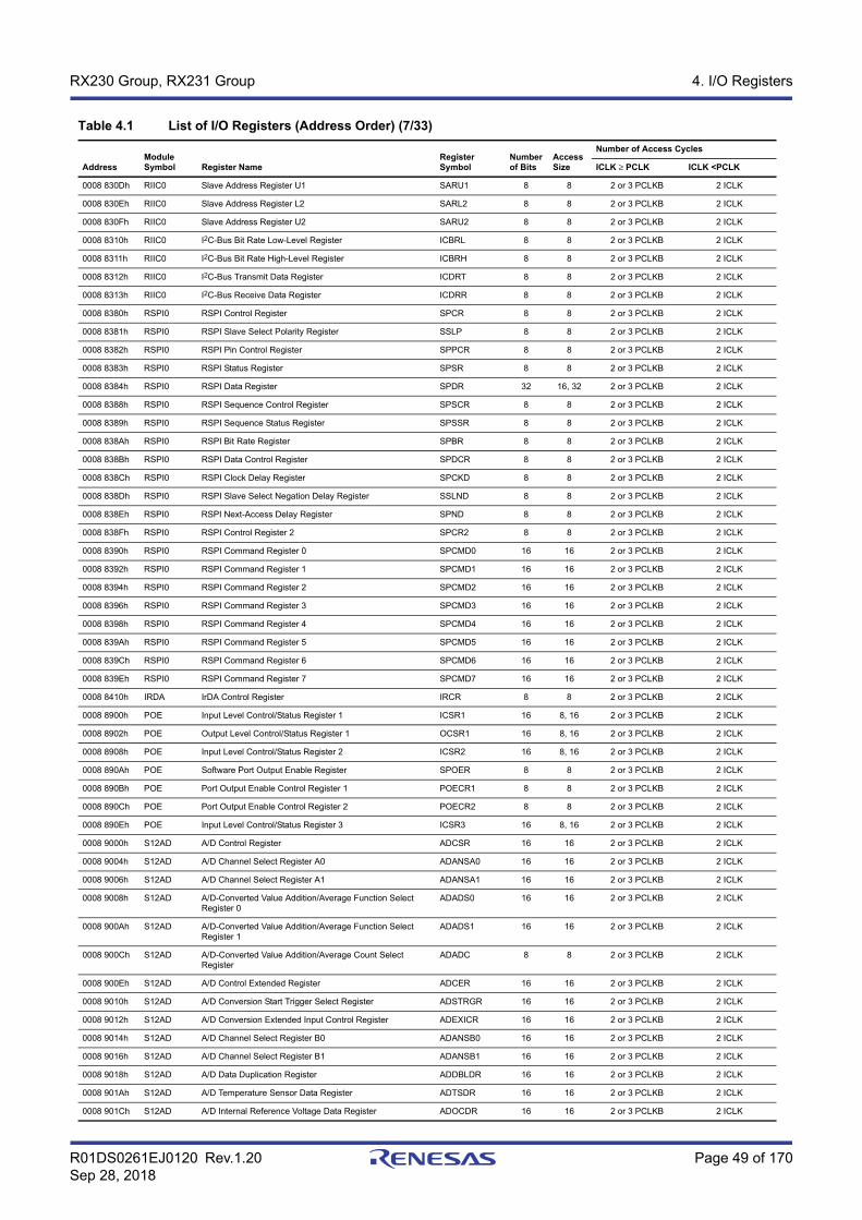
R01DS0261EJ0120 Rev.1.20 Page 49 of 170Sep 28, 2018
RX230 Group, RX231 Group 4. I/O Registers
0008 830Dh RIIC0 Slave Address Register U1 SARU1 8 8 2 or 3 PCLKB 2 ICLK
0008 830Eh RIIC0 Slave Address Register L2 SARL2 8 8 2 or 3 PCLKB 2 ICLK
0008 830Fh RIIC0 Slave Address Register U2 SARU2 8 8 2 or 3 PCLKB 2 ICLK
0008 8310h RIIC0 I2C-Bus Bit Rate Low-Level Register ICBRL 8 8 2 or 3 PCLKB 2 ICLK
0008 8311h RIIC0 I2C-Bus Bit Rate High-Level Register ICBRH 8 8 2 or 3 PCLKB 2 ICLK
0008 8312h RIIC0 I2C-Bus Transmit Data Register ICDRT 8 8 2 or 3 PCLKB 2 ICLK
0008 8313h RIIC0 I2C-Bus Receive Data Register ICDRR 8 8 2 or 3 PCLKB 2 ICLK
0008 8380h RSPI0 RSPI Control Register SPCR 8 8 2 or 3 PCLKB 2 ICLK
0008 8381h RSPI0 RSPI Slave Select Polarity Register SSLP 8 8 2 or 3 PCLKB 2 ICLK
0008 8382h RSPI0 RSPI Pin Control Register SPPCR 8 8 2 or 3 PCLKB 2 ICLK
0008 8383h RSPI0 RSPI Status Register SPSR 8 8 2 or 3 PCLKB 2 ICLK
0008 8384h RSPI0 RSPI Data Register SPDR 32 16, 32 2 or 3 PCLKB 2 ICLK
0008 8388h RSPI0 RSPI Sequence Control Register SPSCR 8 8 2 or 3 PCLKB 2 ICLK
0008 8389h RSPI0 RSPI Sequence Status Register SPSSR 8 8 2 or 3 PCLKB 2 ICLK
0008 838Ah RSPI0 RSPI Bit Rate Register SPBR 8 8 2 or 3 PCLKB 2 ICLK
0008 838Bh RSPI0 RSPI Data Control Register SPDCR 8 8 2 or 3 PCLKB 2 ICLK
0008 838Ch RSPI0 RSPI Clock Delay Register SPCKD 8 8 2 or 3 PCLKB 2 ICLK
0008 838Dh RSPI0 RSPI Slave Select Negation Delay Register SSLND 8 8 2 or 3 PCLKB 2 ICLK
0008 838Eh RSPI0 RSPI Next-Access Delay Register SPND 8 8 2 or 3 PCLKB 2 ICLK
0008 838Fh RSPI0 RSPI Control Register 2 SPCR2 8 8 2 or 3 PCLKB 2 ICLK
0008 8390h RSPI0 RSPI Command Register 0 SPCMD0 16 16 2 or 3 PCLKB 2 ICLK
0008 8392h RSPI0 RSPI Command Register 1 SPCMD1 16 16 2 or 3 PCLKB 2 ICLK
0008 8394h RSPI0 RSPI Command Register 2 SPCMD2 16 16 2 or 3 PCLKB 2 ICLK
0008 8396h RSPI0 RSPI Command Register 3 SPCMD3 16 16 2 or 3 PCLKB 2 ICLK
0008 8398h RSPI0 RSPI Command Register 4 SPCMD4 16 16 2 or 3 PCLKB 2 ICLK
0008 839Ah RSPI0 RSPI Command Register 5 SPCMD5 16 16 2 or 3 PCLKB 2 ICLK
0008 839Ch RSPI0 RSPI Command Register 6 SPCMD6 16 16 2 or 3 PCLKB 2 ICLK
0008 839Eh RSPI0 RSPI Command Register 7 SPCMD7 16 16 2 or 3 PCLKB 2 ICLK
0008 8410h IRDA IrDA Control Register IRCR 8 8 2 or 3 PCLKB 2 ICLK
0008 8900h POE Input Level Control/Status Register 1 ICSR1 16 8, 16 2 or 3 PCLKB 2 ICLK
0008 8902h POE Output Level Control/Status Register 1 OCSR1 16 8, 16 2 or 3 PCLKB 2 ICLK
0008 8908h POE Input Level Control/Status Register 2 ICSR2 16 8, 16 2 or 3 PCLKB 2 ICLK
0008 890Ah POE Software Port Output Enable Register SPOER 8 8 2 or 3 PCLKB 2 ICLK
0008 890Bh POE Port Output Enable Control Register 1 POECR1 8 8 2 or 3 PCLKB 2 ICLK
0008 890Ch POE Port Output Enable Control Register 2 POECR2 8 8 2 or 3 PCLKB 2 ICLK
0008 890Eh POE Input Level Control/Status Register 3 ICSR3 16 8, 16 2 or 3 PCLKB 2 ICLK
0008 9000h S12AD A/D Control Register ADCSR 16 16 2 or 3 PCLKB 2 ICLK
0008 9004h S12AD A/D Channel Select Register A0 ADANSA0 16 16 2 or 3 PCLKB 2 ICLK
0008 9006h S12AD A/D Channel Select Register A1 ADANSA1 16 16 2 or 3 PCLKB 2 ICLK
0008 9008h S12AD A/D-Converted Value Addition/Average Function Select Register 0
ADADS0 16 16 2 or 3 PCLKB 2 ICLK
0008 900Ah S12AD A/D-Converted Value Addition/Average Function Select Register 1
ADADS1 16 16 2 or 3 PCLKB 2 ICLK
0008 900Ch S12AD A/D-Converted Value Addition/Average Count Select Register
ADADC 8 8 2 or 3 PCLKB 2 ICLK
0008 900Eh S12AD A/D Control Extended Register ADCER 16 16 2 or 3 PCLKB 2 ICLK
0008 9010h S12AD A/D Conversion Start Trigger Select Register ADSTRGR 16 16 2 or 3 PCLKB 2 ICLK
0008 9012h S12AD A/D Conversion Extended Input Control Register ADEXICR 16 16 2 or 3 PCLKB 2 ICLK
0008 9014h S12AD A/D Channel Select Register B0 ADANSB0 16 16 2 or 3 PCLKB 2 ICLK
0008 9016h S12AD A/D Channel Select Register B1 ADANSB1 16 16 2 or 3 PCLKB 2 ICLK
0008 9018h S12AD A/D Data Duplication Register ADDBLDR 16 16 2 or 3 PCLKB 2 ICLK
0008 901Ah S12AD A/D Temperature Sensor Data Register ADTSDR 16 16 2 or 3 PCLKB 2 ICLK
0008 901Ch S12AD A/D Internal Reference Voltage Data Register ADOCDR 16 16 2 or 3 PCLKB 2 ICLK
Table 4.1 List of I/O Registers (Address Order) (7/33)
AddressModule Symbol Register Name
Register Symbol
Number of Bits
Access Size
Number of Access Cycles
ICLK ≥ PCLK ICLK <PCLK
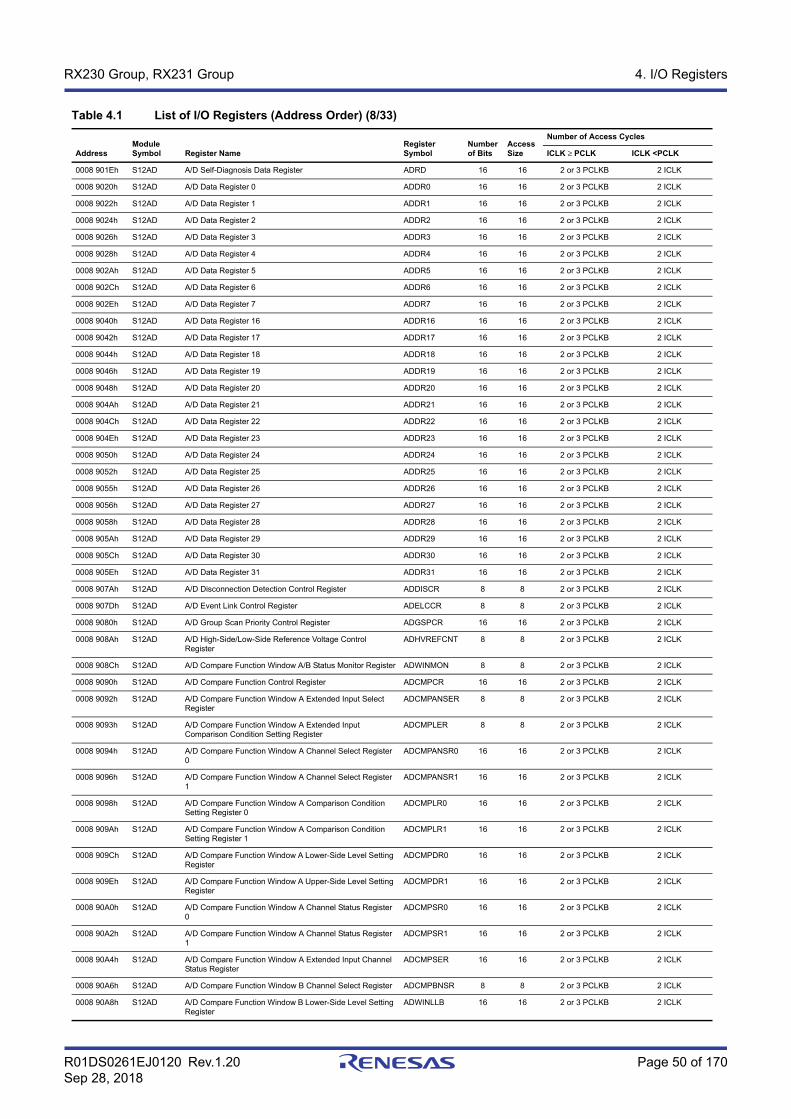
R01DS0261EJ0120 Rev.1.20 Page 50 of 170Sep 28, 2018
RX230 Group, RX231 Group 4. I/O Registers
0008 901Eh S12AD A/D Self-Diagnosis Data Register ADRD 16 16 2 or 3 PCLKB 2 ICLK
0008 9020h S12AD A/D Data Register 0 ADDR0 16 16 2 or 3 PCLKB 2 ICLK
0008 9022h S12AD A/D Data Register 1 ADDR1 16 16 2 or 3 PCLKB 2 ICLK
0008 9024h S12AD A/D Data Register 2 ADDR2 16 16 2 or 3 PCLKB 2 ICLK
0008 9026h S12AD A/D Data Register 3 ADDR3 16 16 2 or 3 PCLKB 2 ICLK
0008 9028h S12AD A/D Data Register 4 ADDR4 16 16 2 or 3 PCLKB 2 ICLK
0008 902Ah S12AD A/D Data Register 5 ADDR5 16 16 2 or 3 PCLKB 2 ICLK
0008 902Ch S12AD A/D Data Register 6 ADDR6 16 16 2 or 3 PCLKB 2 ICLK
0008 902Eh S12AD A/D Data Register 7 ADDR7 16 16 2 or 3 PCLKB 2 ICLK
0008 9040h S12AD A/D Data Register 16 ADDR16 16 16 2 or 3 PCLKB 2 ICLK
0008 9042h S12AD A/D Data Register 17 ADDR17 16 16 2 or 3 PCLKB 2 ICLK
0008 9044h S12AD A/D Data Register 18 ADDR18 16 16 2 or 3 PCLKB 2 ICLK
0008 9046h S12AD A/D Data Register 19 ADDR19 16 16 2 or 3 PCLKB 2 ICLK
0008 9048h S12AD A/D Data Register 20 ADDR20 16 16 2 or 3 PCLKB 2 ICLK
0008 904Ah S12AD A/D Data Register 21 ADDR21 16 16 2 or 3 PCLKB 2 ICLK
0008 904Ch S12AD A/D Data Register 22 ADDR22 16 16 2 or 3 PCLKB 2 ICLK
0008 904Eh S12AD A/D Data Register 23 ADDR23 16 16 2 or 3 PCLKB 2 ICLK
0008 9050h S12AD A/D Data Register 24 ADDR24 16 16 2 or 3 PCLKB 2 ICLK
0008 9052h S12AD A/D Data Register 25 ADDR25 16 16 2 or 3 PCLKB 2 ICLK
0008 9055h S12AD A/D Data Register 26 ADDR26 16 16 2 or 3 PCLKB 2 ICLK
0008 9056h S12AD A/D Data Register 27 ADDR27 16 16 2 or 3 PCLKB 2 ICLK
0008 9058h S12AD A/D Data Register 28 ADDR28 16 16 2 or 3 PCLKB 2 ICLK
0008 905Ah S12AD A/D Data Register 29 ADDR29 16 16 2 or 3 PCLKB 2 ICLK
0008 905Ch S12AD A/D Data Register 30 ADDR30 16 16 2 or 3 PCLKB 2 ICLK
0008 905Eh S12AD A/D Data Register 31 ADDR31 16 16 2 or 3 PCLKB 2 ICLK
0008 907Ah S12AD A/D Disconnection Detection Control Register ADDISCR 8 8 2 or 3 PCLKB 2 ICLK
0008 907Dh S12AD A/D Event Link Control Register ADELCCR 8 8 2 or 3 PCLKB 2 ICLK
0008 9080h S12AD A/D Group Scan Priority Control Register ADGSPCR 16 16 2 or 3 PCLKB 2 ICLK
0008 908Ah S12AD A/D High-Side/Low-Side Reference Voltage Control Register
ADHVREFCNT 8 8 2 or 3 PCLKB 2 ICLK
0008 908Ch S12AD A/D Compare Function Window A/B Status Monitor Register ADWINMON 8 8 2 or 3 PCLKB 2 ICLK
0008 9090h S12AD A/D Compare Function Control Register ADCMPCR 16 16 2 or 3 PCLKB 2 ICLK
0008 9092h S12AD A/D Compare Function Window A Extended Input Select Register
ADCMPANSER 8 8 2 or 3 PCLKB 2 ICLK
0008 9093h S12AD A/D Compare Function Window A Extended Input Comparison Condition Setting Register
ADCMPLER 8 8 2 or 3 PCLKB 2 ICLK
0008 9094h S12AD A/D Compare Function Window A Channel Select Register 0
ADCMPANSR0 16 16 2 or 3 PCLKB 2 ICLK
0008 9096h S12AD A/D Compare Function Window A Channel Select Register 1
ADCMPANSR1 16 16 2 or 3 PCLKB 2 ICLK
0008 9098h S12AD A/D Compare Function Window A Comparison Condition Setting Register 0
ADCMPLR0 16 16 2 or 3 PCLKB 2 ICLK
0008 909Ah S12AD A/D Compare Function Window A Comparison Condition Setting Register 1
ADCMPLR1 16 16 2 or 3 PCLKB 2 ICLK
0008 909Ch S12AD A/D Compare Function Window A Lower-Side Level Setting Register
ADCMPDR0 16 16 2 or 3 PCLKB 2 ICLK
0008 909Eh S12AD A/D Compare Function Window A Upper-Side Level Setting Register
ADCMPDR1 16 16 2 or 3 PCLKB 2 ICLK
0008 90A0h S12AD A/D Compare Function Window A Channel Status Register 0
ADCMPSR0 16 16 2 or 3 PCLKB 2 ICLK
0008 90A2h S12AD A/D Compare Function Window A Channel Status Register 1
ADCMPSR1 16 16 2 or 3 PCLKB 2 ICLK
0008 90A4h S12AD A/D Compare Function Window A Extended Input Channel Status Register
ADCMPSER 16 16 2 or 3 PCLKB 2 ICLK
0008 90A6h S12AD A/D Compare Function Window B Channel Select Register ADCMPBNSR 8 8 2 or 3 PCLKB 2 ICLK
0008 90A8h S12AD A/D Compare Function Window B Lower-Side Level Setting Register
ADWINLLB 16 16 2 or 3 PCLKB 2 ICLK
Table 4.1 List of I/O Registers (Address Order) (8/33)
AddressModule Symbol Register Name
Register Symbol
Number of Bits
Access Size
Number of Access Cycles
ICLK ≥ PCLK ICLK <PCLK
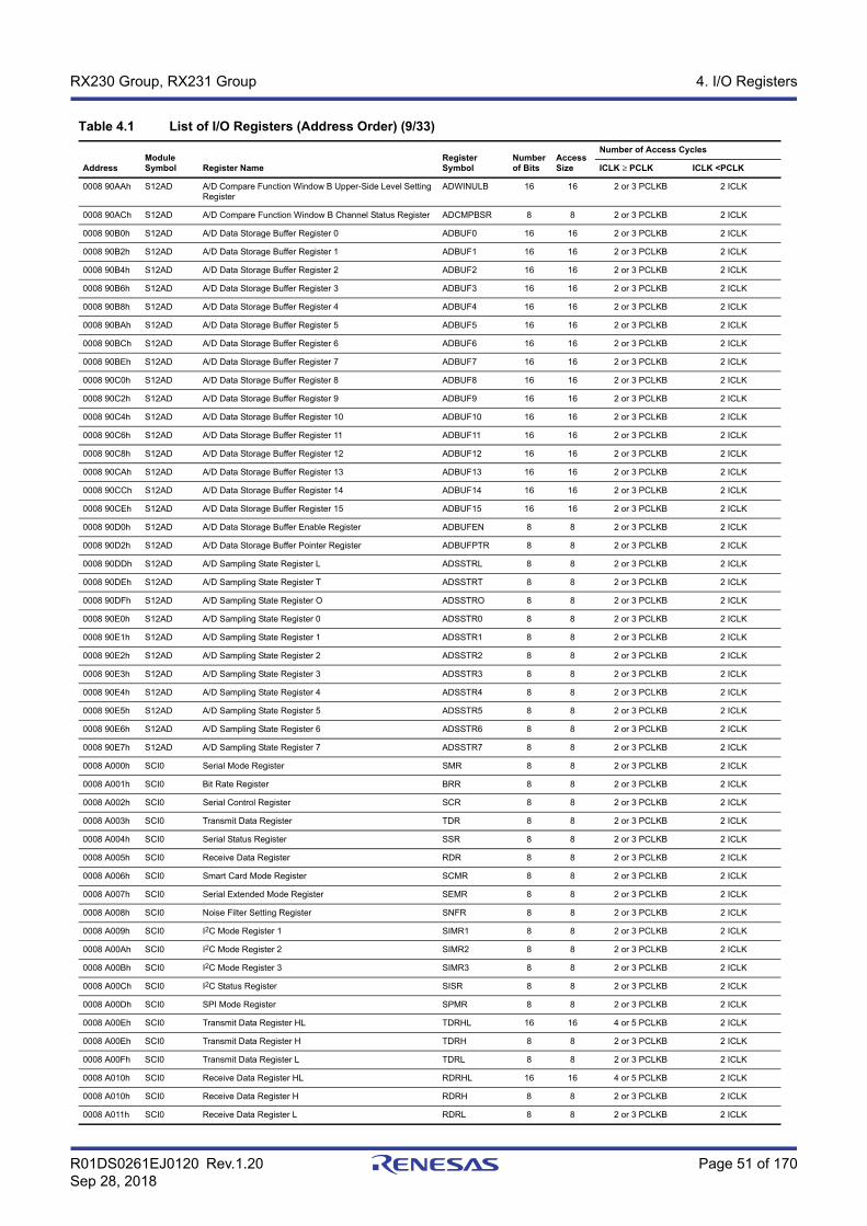
R01DS0261EJ0120 Rev.1.20 Page 51 of 170Sep 28, 2018
RX230 Group, RX231 Group 4. I/O Registers
0008 90AAh S12AD A/D Compare Function Window B Upper-Side Level Setting Register
ADWINULB 16 16 2 or 3 PCLKB 2 ICLK
0008 90ACh S12AD A/D Compare Function Window B Channel Status Register ADCMPBSR 8 8 2 or 3 PCLKB 2 ICLK
0008 90B0h S12AD A/D Data Storage Buffer Register 0 ADBUF0 16 16 2 or 3 PCLKB 2 ICLK
0008 90B2h S12AD A/D Data Storage Buffer Register 1 ADBUF1 16 16 2 or 3 PCLKB 2 ICLK
0008 90B4h S12AD A/D Data Storage Buffer Register 2 ADBUF2 16 16 2 or 3 PCLKB 2 ICLK
0008 90B6h S12AD A/D Data Storage Buffer Register 3 ADBUF3 16 16 2 or 3 PCLKB 2 ICLK
0008 90B8h S12AD A/D Data Storage Buffer Register 4 ADBUF4 16 16 2 or 3 PCLKB 2 ICLK
0008 90BAh S12AD A/D Data Storage Buffer Register 5 ADBUF5 16 16 2 or 3 PCLKB 2 ICLK
0008 90BCh S12AD A/D Data Storage Buffer Register 6 ADBUF6 16 16 2 or 3 PCLKB 2 ICLK
0008 90BEh S12AD A/D Data Storage Buffer Register 7 ADBUF7 16 16 2 or 3 PCLKB 2 ICLK
0008 90C0h S12AD A/D Data Storage Buffer Register 8 ADBUF8 16 16 2 or 3 PCLKB 2 ICLK
0008 90C2h S12AD A/D Data Storage Buffer Register 9 ADBUF9 16 16 2 or 3 PCLKB 2 ICLK
0008 90C4h S12AD A/D Data Storage Buffer Register 10 ADBUF10 16 16 2 or 3 PCLKB 2 ICLK
0008 90C6h S12AD A/D Data Storage Buffer Register 11 ADBUF11 16 16 2 or 3 PCLKB 2 ICLK
0008 90C8h S12AD A/D Data Storage Buffer Register 12 ADBUF12 16 16 2 or 3 PCLKB 2 ICLK
0008 90CAh S12AD A/D Data Storage Buffer Register 13 ADBUF13 16 16 2 or 3 PCLKB 2 ICLK
0008 90CCh S12AD A/D Data Storage Buffer Register 14 ADBUF14 16 16 2 or 3 PCLKB 2 ICLK
0008 90CEh S12AD A/D Data Storage Buffer Register 15 ADBUF15 16 16 2 or 3 PCLKB 2 ICLK
0008 90D0h S12AD A/D Data Storage Buffer Enable Register ADBUFEN 8 8 2 or 3 PCLKB 2 ICLK
0008 90D2h S12AD A/D Data Storage Buffer Pointer Register ADBUFPTR 8 8 2 or 3 PCLKB 2 ICLK
0008 90DDh S12AD A/D Sampling State Register L ADSSTRL 8 8 2 or 3 PCLKB 2 ICLK
0008 90DEh S12AD A/D Sampling State Register T ADSSTRT 8 8 2 or 3 PCLKB 2 ICLK
0008 90DFh S12AD A/D Sampling State Register O ADSSTRO 8 8 2 or 3 PCLKB 2 ICLK
0008 90E0h S12AD A/D Sampling State Register 0 ADSSTR0 8 8 2 or 3 PCLKB 2 ICLK
0008 90E1h S12AD A/D Sampling State Register 1 ADSSTR1 8 8 2 or 3 PCLKB 2 ICLK
0008 90E2h S12AD A/D Sampling State Register 2 ADSSTR2 8 8 2 or 3 PCLKB 2 ICLK
0008 90E3h S12AD A/D Sampling State Register 3 ADSSTR3 8 8 2 or 3 PCLKB 2 ICLK
0008 90E4h S12AD A/D Sampling State Register 4 ADSSTR4 8 8 2 or 3 PCLKB 2 ICLK
0008 90E5h S12AD A/D Sampling State Register 5 ADSSTR5 8 8 2 or 3 PCLKB 2 ICLK
0008 90E6h S12AD A/D Sampling State Register 6 ADSSTR6 8 8 2 or 3 PCLKB 2 ICLK
0008 90E7h S12AD A/D Sampling State Register 7 ADSSTR7 8 8 2 or 3 PCLKB 2 ICLK
0008 A000h SCI0 Serial Mode Register SMR 8 8 2 or 3 PCLKB 2 ICLK
0008 A001h SCI0 Bit Rate Register BRR 8 8 2 or 3 PCLKB 2 ICLK
0008 A002h SCI0 Serial Control Register SCR 8 8 2 or 3 PCLKB 2 ICLK
0008 A003h SCI0 Transmit Data Register TDR 8 8 2 or 3 PCLKB 2 ICLK
0008 A004h SCI0 Serial Status Register SSR 8 8 2 or 3 PCLKB 2 ICLK
0008 A005h SCI0 Receive Data Register RDR 8 8 2 or 3 PCLKB 2 ICLK
0008 A006h SCI0 Smart Card Mode Register SCMR 8 8 2 or 3 PCLKB 2 ICLK
0008 A007h SCI0 Serial Extended Mode Register SEMR 8 8 2 or 3 PCLKB 2 ICLK
0008 A008h SCI0 Noise Filter Setting Register SNFR 8 8 2 or 3 PCLKB 2 ICLK
0008 A009h SCI0 I2C Mode Register 1 SIMR1 8 8 2 or 3 PCLKB 2 ICLK
0008 A00Ah SCI0 I2C Mode Register 2 SIMR2 8 8 2 or 3 PCLKB 2 ICLK
0008 A00Bh SCI0 I2C Mode Register 3 SIMR3 8 8 2 or 3 PCLKB 2 ICLK
0008 A00Ch SCI0 I2C Status Register SISR 8 8 2 or 3 PCLKB 2 ICLK
0008 A00Dh SCI0 SPI Mode Register SPMR 8 8 2 or 3 PCLKB 2 ICLK
0008 A00Eh SCI0 Transmit Data Register HL TDRHL 16 16 4 or 5 PCLKB 2 ICLK
0008 A00Eh SCI0 Transmit Data Register H TDRH 8 8 2 or 3 PCLKB 2 ICLK
0008 A00Fh SCI0 Transmit Data Register L TDRL 8 8 2 or 3 PCLKB 2 ICLK
0008 A010h SCI0 Receive Data Register HL RDRHL 16 16 4 or 5 PCLKB 2 ICLK
0008 A010h SCI0 Receive Data Register H RDRH 8 8 2 or 3 PCLKB 2 ICLK
0008 A011h SCI0 Receive Data Register L RDRL 8 8 2 or 3 PCLKB 2 ICLK
Table 4.1 List of I/O Registers (Address Order) (9/33)
AddressModule Symbol Register Name
Register Symbol
Number of Bits
Access Size
Number of Access Cycles
ICLK ≥ PCLK ICLK <PCLK

R01DS0261EJ0120 Rev.1.20 Page 52 of 170Sep 28, 2018
RX230 Group, RX231 Group 4. I/O Registers
0008 A012h SCI0 Modulation Duty Register MDDR 8 8 2 or 3 PCLKB 2 ICLK
0008 A020h SCI1 Serial Mode Register SMR 8 8 2 or 3 PCLKB 2 ICLK
0008 A021h SCI1 Bit Rate Register BRR 8 8 2 or 3 PCLKB 2 ICLK
0008 A022h SCI1 Serial Control Register SCR 8 8 2 or 3 PCLKB 2 ICLK
0008 A023h SCI1 Transmit Data Register TDR 8 8 2 or 3 PCLKB 2 ICLK
0008 A024h SCI1 Serial Status Register SSR 8 8 2 or 3 PCLKB 2 ICLK
0008 A025h SCI1 Receive Data Register RDR 8 8 2 or 3 PCLKB 2 ICLK
0008 A026h SCI1 Smart Card Mode Register SCMR 8 8 2 or 3 PCLKB 2 ICLK
0008 A027h SCI1 Serial Extended Mode Register SEMR 8 8 2 or 3 PCLKB 2 ICLK
0008 A028h SCI1 Noise Filter Setting Register SNFR 8 8 2 or 3 PCLKB 2 ICLK
0008 A029h SCI1 I2C Mode Register 1 SIMR1 8 8 2 or 3 PCLKB 2 ICLK
0008 A02Ah SCI1 I2C Mode Register 2 SIMR2 8 8 2 or 3 PCLKB 2 ICLK
0008 A02Bh SCI1 I2C Mode Register 3 SIMR3 8 8 2 or 3 PCLKB 2 ICLK
0008 A02Ch SCI1 I2C Status Register SISR 8 8 2 or 3 PCLKB 2 ICLK
0008 A02Dh SCI1 SPI Mode Register SPMR 8 8 2 or 3 PCLKB 2 ICLK
0008 A02Eh SCI1 Transmit Data Register HL TDRHL 16 16 4 or 5 PCLKB 2 ICLK
0008 A02Eh SCI1 Transmit Data Register H TDRH 8 8 2 or 3 PCLKB 2 ICLK
0008 A02Fh SCI1 Transmit Data Register L TDRL 8 8 2 or 3 PCLKB 2 ICLK
0008 A030h SCI1 Receive Data Register HL RDRHL 16 16 4 or 5 PCLKB 2 ICLK
0008 A030h SCI1 Receive Data Register H RDRH 8 8 2 or 3 PCLKB 2 ICLK
0008 A031h SCI1 Receive Data Register L RDRL 8 8 2 or 3 PCLKB 2 ICLK
0008 A032h SCI1 Modulation Duty Register MDDR 8 8 2 or 3 PCLKB 2 ICLK
0008 A0A0h SCI5 Serial Mode Register SMR 8 8 2 or 3 PCLKB 2 ICLK
0008 A0A1h SCI5 Bit Rate Register BRR 8 8 2 or 3 PCLKB 2 ICLK
0008 A0A2h SCI5 Serial Control Register SCR 8 8 2 or 3 PCLKB 2 ICLK
0008 A0A3h SCI5 Transmit Data Register TDR 8 8 2 or 3 PCLKB 2 ICLK
0008 A0A4h SCI5 Serial Status Register SSR 8 8 2 or 3 PCLKB 2 ICLK
0008 A0A5h SCI5 Receive Data Register RDR 8 8 2 or 3 PCLKB 2 ICLK
0008 A0A6h SCI5 Smart Card Mode Register SCMR 8 8 2 or 3 PCLKB 2 ICLK
0008 A0A7h SCI5 Serial Extended Mode Register SEMR 8 8 2 or 3 PCLKB 2 ICLK
0008 A0A8h SCI5 Noise Filter Setting Register SNFR 8 8 2 or 3 PCLKB 2 ICLK
0008 A0A9h SCI5 I2C Mode Register 1 SIMR1 8 8 2 or 3 PCLKB 2 ICLK
0008 A0AAh SCI5 I2C Mode Register 2 SIMR2 8 8 2 or 3 PCLKB 2 ICLK
0008 A0ABh SCI5 I2C Mode Register 3 SIMR3 8 8 2 or 3 PCLKB 2 ICLK
0008 A0ACh SCI5 I2C Status Register SISR 8 8 2 or 3 PCLKB 2 ICLK
0008 A0ADh SCI5 SPI Mode Register SPMR 8 8 2 or 3 PCLKB 2 ICLK
0008 A0AEh SCI5 Transmit Data Register HL TDRHL 16 16 4 or 5 PCLKB 2 ICLK
0008 A0AEh SCI5 Transmit Data Register H TDRH 8 8 2 or 3 PCLKB 2 ICLK
0008 A0AFh SCI5 Transmit Data Register L TDRL 8 8 2 or 3 PCLKB 2 ICLK
0008 A0B0h SCI5 Receive Data Register HL RDRHL 16 16 4 or 5 PCLKB 2 ICLK
0008 A0B0h SCI5 Receive Data Register H RDRH 8 8 2 or 3 PCLKB 2 ICLK
0008 A0B1h SCI5 Receive Data Register L RDRL 8 8 2 or 3 PCLKB 2 ICLK
0008 A0B2h SCI5 Modulation Duty Register MDDR 8 8 2 or 3 PCLKB 2 ICLK
0008 A0C0h SCI6 Serial Mode Register SMR 8 8 2 or 3 PCLKB 2 ICLK
0008 A0C1h SCI6 Bit Rate Register BRR 8 8 2 or 3 PCLKB 2 ICLK
0008 A0C2h SCI6 Serial Control Register SCR 8 8 2 or 3 PCLKB 2 ICLK
0008 A0C3h SCI6 Transmit Data Register TDR 8 8 2 or 3 PCLKB 2 ICLK
0008 A0C4h SCI6 Serial Status Register SSR 8 8 2 or 3 PCLKB 2 ICLK
0008 A0C5h SCI6 Receive Data Register RDR 8 8 2 or 3 PCLKB 2 ICLK
0008 A0C6h SCI6 Smart Card Mode Register SCMR 8 8 2 or 3 PCLKB 2 ICLK
0008 A0C7h SCI6 Serial Extended Mode Register SEMR 8 8 2 or 3 PCLKB 2 ICLK
0008 A0C8h SCI6 Noise Filter Setting Register SNFR 8 8 2 or 3 PCLKB 2 ICLK
Table 4.1 List of I/O Registers (Address Order) (10/33)
AddressModule Symbol Register Name
Register Symbol
Number of Bits
Access Size
Number of Access Cycles
ICLK ≥ PCLK ICLK <PCLK

R01DS0261EJ0120 Rev.1.20 Page 53 of 170Sep 28, 2018
RX230 Group, RX231 Group 4. I/O Registers
0008 A0C9h SCI6 I2C Mode Register 1 SIMR1 8 8 2 or 3 PCLKB 2 ICLK
0008 A0CAh SCI6 I2C Mode Register 2 SIMR2 8 8 2 or 3 PCLKB 2 ICLK
0008 A0CBh SCI6 I2C Mode Register 3 SIMR3 8 8 2 or 3 PCLKB 2 ICLK
0008 A0CCh SCI6 I2C Status Register SISR 8 8 2 or 3 PCLKB 2 ICLK
0008 A0CDh SCI6 SPI Mode Register SPMR 8 8 2 or 3 PCLKB 2 ICLK
0008 A0CEh SCI6 Transmit Data Register HL TDRHL 16 16 4 or 5 PCLKB 2 ICLK
0008 A0CEh SCI6 Transmit Data Register H TDRH 8 8 2 or 3 PCLKB 2 ICLK
0008 A0CFh SCI6 Transmit Data Register L TDRL 8 8 2 or 3 PCLKB 2 ICLK
0008 A0D0h SCI6 Receive Data Register HL RDRHL 16 16 4 or 5 PCLKB 2 ICLK
0008 A0D0h SCI6 Receive Data Register H RDRH 8 8 2 or 3 PCLKB 2 ICLK
0008 A0D1h SCI6 Receive Data Register L RDRL 8 8 2 or 3 PCLKB 2 ICLK
0008 A0D2h SCI6 Modulation Duty Register MDDR 8 8 2 or 3 PCLKB 2 ICLK
0008 A100h SCI8 Serial Mode Register SMR 8 8 2 or 3 PCLKB 2 ICLK
0008 A101h SCI8 Bit Rate Register BRR 8 8 2 or 3 PCLKB 2 ICLK
0008 A102h SCI8 Serial Control Register SCR 8 8 2 or 3 PCLKB 2 ICLK
0008 A103h SCI8 Transmit Data Register TDR 8 8 2 or 3 PCLKB 2 ICLK
0008 A104h SCI8 Serial Status Register SSR 8 8 2 or 3 PCLKB 2 ICLK
0008 A105h SCI8 Receive Data Register RDR 8 8 2 or 3 PCLKB 2 ICLK
0008 A106h SCI8 Smart Card Mode Register SCMR 8 8 2 or 3 PCLKB 2 ICLK
0008 A107h SCI8 Serial Extended Mode Register SEMR 8 8 2 or 3 PCLKB 2 ICLK
0008 A108h SCI8 Noise Filter Setting Register SNFR 8 8 2 or 3 PCLKB 2 ICLK
0008 A109h SCI8 I2C Mode Register 1 SIMR1 8 8 2 or 3 PCLKB 2 ICLK
0008 A10Ah SCI8 I2C Mode Register 2 SIMR2 8 8 2 or 3 PCLKB 2 ICLK
0008 A10Bh SCI8 I2C Mode Register 3 SIMR3 8 8 2 or 3 PCLKB 2 ICLK
0008 A10Ch SCI8 I2C Status Register SISR 8 8 2 or 3 PCLKB 2 ICLK
0008 A10Dh SCI8 SPI Mode Register SPMR 8 8 2 or 3 PCLKB 2 ICLK
0008 A10Eh SCI8 Transmit Data Register HL TDRHL 16 16 4 or 5 PCLKB 2 ICLK
0008 A10Eh SCI8 Transmit Data Register H TDRH 8 8 2 or 3 PCLKB 2 ICLK
0008 A10Fh SCI8 Transmit Data Register L TDRL 8 8 2 or 3 PCLKB 2 ICLK
0008 A110h SCI8 Receive Data Register HL RDRHL 16 16 4 or 5 PCLKB 2 ICLK
0008 A110h SCI8 Receive Data Register H RDRH 8 8 2 or 3 PCLKB 2 ICLK
0008 A111h SCI8 Receive Data Register L RDRL 8 8 2 or 3 PCLKB 2 ICLK
0008 A112h SCI8 Modulation Duty Register MDDR 8 8 2 or 3 PCLKB 2 ICLK
0008 A120h SCI9 Serial Mode Register SMR 8 8 2 or 3 PCLKB 2 ICLK
0008 A121h SCI9 Bit Rate Register BRR 8 8 2 or 3 PCLKB 2 ICLK
0008 A122h SCI9 Serial Control Register SCR 8 8 2 or 3 PCLKB 2 ICLK
0008 A123h SCI9 Transmit Data Register TDR 8 8 2 or 3 PCLKB 2 ICLK
0008 A124h SCI9 Serial Status Register SSR 8 8 2 or 3 PCLKB 2 ICLK
0008 A125h SCI9 Receive Data Register RDR 8 8 2 or 3 PCLKB 2 ICLK
0008 A126h SCI9 Smart Card Mode Register SCMR 8 8 2 or 3 PCLKB 2 ICLK
0008 A127h SCI9 Serial Extended Mode Register SEMR 8 8 2 or 3 PCLKB 2 ICLK
0008 A128h SCI9 Noise Filter Setting Register SNFR 8 8 2 or 3 PCLKB 2 ICLK
0008 A129h SCI9 I2C Mode Register 1 SIMR1 8 8 2 or 3 PCLKB 2 ICLK
0008 A12Ah SCI9 I2C Mode Register 2 SIMR2 8 8 2 or 3 PCLKB 2 ICLK
0008 A12Bh SCI9 I2C Mode Register 3 SIMR3 8 8 2 or 3 PCLKB 2 ICLK
0008 A12Ch SCI9 I2C Status Register SISR 8 8 2 or 3 PCLKB 2 ICLK
0008 A12Dh SCI9 SPI Mode Register SPMR 8 8 2 or 3 PCLKB 2 ICLK
0008 A12Eh SCI9 Transmit Data Register HL TDRHL 16 16 4 or 5 PCLKB 2 ICLK
0008 A12Eh SCI9 Transmit Data Register H TDRH 8 8 2 or 3 PCLKB 2 ICLK
0008 A12Fh SCI9 Transmit Data Register L TDRL 8 8 2 or 3 PCLKB 2 ICLK
0008 A130h SCI9 Receive Data Register HL RDRHL 16 16 4 or 5 PCLKB 2 ICLK
0008 A130h SCI9 Receive Data Register H RDRH 8 8 2 or 3 PCLKB 2 ICLK
Table 4.1 List of I/O Registers (Address Order) (11/33)
AddressModule Symbol Register Name
Register Symbol
Number of Bits
Access Size
Number of Access Cycles
ICLK ≥ PCLK ICLK <PCLK
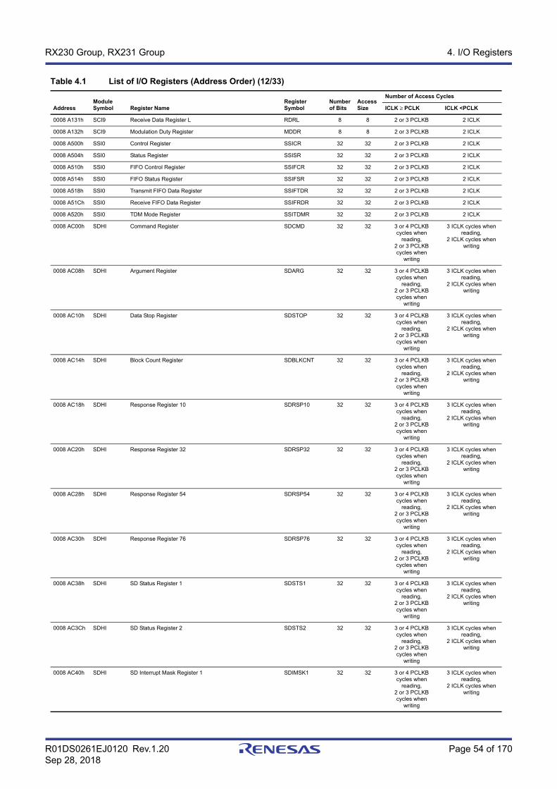
R01DS0261EJ0120 Rev.1.20 Page 54 of 170Sep 28, 2018
RX230 Group, RX231 Group 4. I/O Registers
0008 A131h SCI9 Receive Data Register L RDRL 8 8 2 or 3 PCLKB 2 ICLK
0008 A132h SCI9 Modulation Duty Register MDDR 8 8 2 or 3 PCLKB 2 ICLK
0008 A500h SSI0 Control Register SSICR 32 32 2 or 3 PCLKB 2 ICLK
0008 A504h SSI0 Status Register SSISR 32 32 2 or 3 PCLKB 2 ICLK
0008 A510h SSI0 FIFO Control Register SSIFCR 32 32 2 or 3 PCLKB 2 ICLK
0008 A514h SSI0 FIFO Status Register SSIFSR 32 32 2 or 3 PCLKB 2 ICLK
0008 A518h SSI0 Transmit FIFO Data Register SSIFTDR 32 32 2 or 3 PCLKB 2 ICLK
0008 A51Ch SSI0 Receive FIFO Data Register SSIFRDR 32 32 2 or 3 PCLKB 2 ICLK
0008 A520h SSI0 TDM Mode Register SSITDMR 32 32 2 or 3 PCLKB 2 ICLK
0008 AC00h SDHI Command Register SDCMD 32 32 3 or 4 PCLKBcycles when
reading,2 or 3 PCLKBcycles when
writing
3 ICLK cycles when reading,
2 ICLK cycles when writing
0008 AC08h SDHI Argument Register SDARG 32 32 3 or 4 PCLKBcycles when
reading,2 or 3 PCLKBcycles when
writing
3 ICLK cycles when reading,
2 ICLK cycles when writing
0008 AC10h SDHI Data Stop Register SDSTOP 32 32 3 or 4 PCLKBcycles when
reading,2 or 3 PCLKBcycles when
writing
3 ICLK cycles when reading,
2 ICLK cycles when writing
0008 AC14h SDHI Block Count Register SDBLKCNT 32 32 3 or 4 PCLKBcycles when
reading,2 or 3 PCLKBcycles when
writing
3 ICLK cycles when reading,
2 ICLK cycles when writing
0008 AC18h SDHI Response Register 10 SDRSP10 32 32 3 or 4 PCLKBcycles when
reading,2 or 3 PCLKBcycles when
writing
3 ICLK cycles when reading,
2 ICLK cycles when writing
0008 AC20h SDHI Response Register 32 SDRSP32 32 32 3 or 4 PCLKBcycles when
reading,2 or 3 PCLKBcycles when
writing
3 ICLK cycles when reading,
2 ICLK cycles when writing
0008 AC28h SDHI Response Register 54 SDRSP54 32 32 3 or 4 PCLKBcycles when
reading,2 or 3 PCLKBcycles when
writing
3 ICLK cycles when reading,
2 ICLK cycles when writing
0008 AC30h SDHI Response Register 76 SDRSP76 32 32 3 or 4 PCLKBcycles when
reading,2 or 3 PCLKBcycles when
writing
3 ICLK cycles when reading,
2 ICLK cycles when writing
0008 AC38h SDHI SD Status Register 1 SDSTS1 32 32 3 or 4 PCLKBcycles when
reading,2 or 3 PCLKBcycles when
writing
3 ICLK cycles when reading,
2 ICLK cycles when writing
0008 AC3Ch SDHI SD Status Register 2 SDSTS2 32 32 3 or 4 PCLKBcycles when
reading,2 or 3 PCLKBcycles when
writing
3 ICLK cycles when reading,
2 ICLK cycles when writing
0008 AC40h SDHI SD Interrupt Mask Register 1 SDIMSK1 32 32 3 or 4 PCLKBcycles when
reading,2 or 3 PCLKBcycles when
writing
3 ICLK cycles when reading,
2 ICLK cycles when writing
Table 4.1 List of I/O Registers (Address Order) (12/33)
AddressModule Symbol Register Name
Register Symbol
Number of Bits
Access Size
Number of Access Cycles
ICLK ≥ PCLK ICLK <PCLK
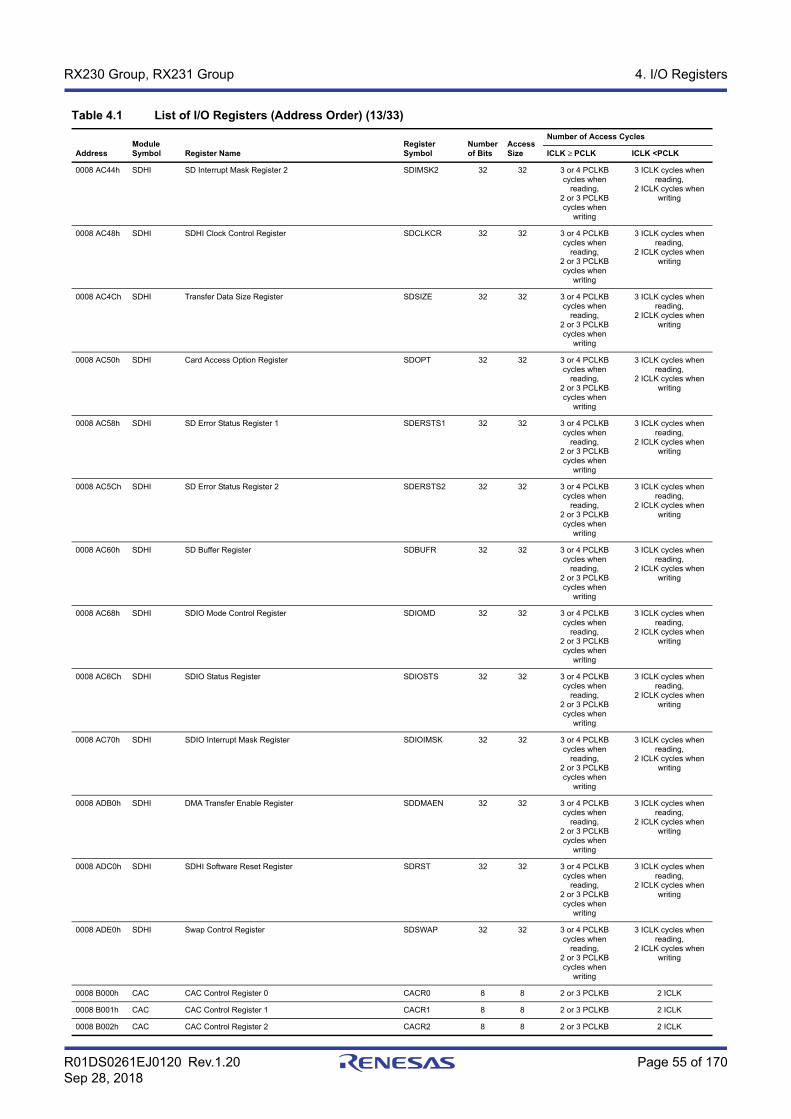
R01DS0261EJ0120 Rev.1.20 Page 55 of 170Sep 28, 2018
RX230 Group, RX231 Group 4. I/O Registers
0008 AC44h SDHI SD Interrupt Mask Register 2 SDIMSK2 32 32 3 or 4 PCLKBcycles when
reading,2 or 3 PCLKBcycles when
writing
3 ICLK cycles when reading,
2 ICLK cycles when writing
0008 AC48h SDHI SDHI Clock Control Register SDCLKCR 32 32 3 or 4 PCLKBcycles when
reading,2 or 3 PCLKBcycles when
writing
3 ICLK cycles when reading,
2 ICLK cycles when writing
0008 AC4Ch SDHI Transfer Data Size Register SDSIZE 32 32 3 or 4 PCLKBcycles when
reading,2 or 3 PCLKBcycles when
writing
3 ICLK cycles when reading,
2 ICLK cycles when writing
0008 AC50h SDHI Card Access Option Register SDOPT 32 32 3 or 4 PCLKBcycles when
reading,2 or 3 PCLKBcycles when
writing
3 ICLK cycles when reading,
2 ICLK cycles when writing
0008 AC58h SDHI SD Error Status Register 1 SDERSTS1 32 32 3 or 4 PCLKBcycles when
reading,2 or 3 PCLKBcycles when
writing
3 ICLK cycles when reading,
2 ICLK cycles when writing
0008 AC5Ch SDHI SD Error Status Register 2 SDERSTS2 32 32 3 or 4 PCLKBcycles when
reading,2 or 3 PCLKBcycles when
writing
3 ICLK cycles when reading,
2 ICLK cycles when writing
0008 AC60h SDHI SD Buffer Register SDBUFR 32 32 3 or 4 PCLKBcycles when
reading,2 or 3 PCLKBcycles when
writing
3 ICLK cycles when reading,
2 ICLK cycles when writing
0008 AC68h SDHI SDIO Mode Control Register SDIOMD 32 32 3 or 4 PCLKBcycles when
reading,2 or 3 PCLKBcycles when
writing
3 ICLK cycles when reading,
2 ICLK cycles when writing
0008 AC6Ch SDHI SDIO Status Register SDIOSTS 32 32 3 or 4 PCLKBcycles when
reading,2 or 3 PCLKBcycles when
writing
3 ICLK cycles when reading,
2 ICLK cycles when writing
0008 AC70h SDHI SDIO Interrupt Mask Register SDIOIMSK 32 32 3 or 4 PCLKBcycles when
reading,2 or 3 PCLKBcycles when
writing
3 ICLK cycles when reading,
2 ICLK cycles when writing
0008 ADB0h SDHI DMA Transfer Enable Register SDDMAEN 32 32 3 or 4 PCLKBcycles when
reading,2 or 3 PCLKBcycles when
writing
3 ICLK cycles when reading,
2 ICLK cycles when writing
0008 ADC0h SDHI SDHI Software Reset Register SDRST 32 32 3 or 4 PCLKBcycles when
reading,2 or 3 PCLKBcycles when
writing
3 ICLK cycles when reading,
2 ICLK cycles when writing
0008 ADE0h SDHI Swap Control Register SDSWAP 32 32 3 or 4 PCLKBcycles when
reading,2 or 3 PCLKBcycles when
writing
3 ICLK cycles when reading,
2 ICLK cycles when writing
0008 B000h CAC CAC Control Register 0 CACR0 8 8 2 or 3 PCLKB 2 ICLK
0008 B001h CAC CAC Control Register 1 CACR1 8 8 2 or 3 PCLKB 2 ICLK
0008 B002h CAC CAC Control Register 2 CACR2 8 8 2 or 3 PCLKB 2 ICLK
Table 4.1 List of I/O Registers (Address Order) (13/33)
AddressModule Symbol Register Name
Register Symbol
Number of Bits
Access Size
Number of Access Cycles
ICLK ≥ PCLK ICLK <PCLK
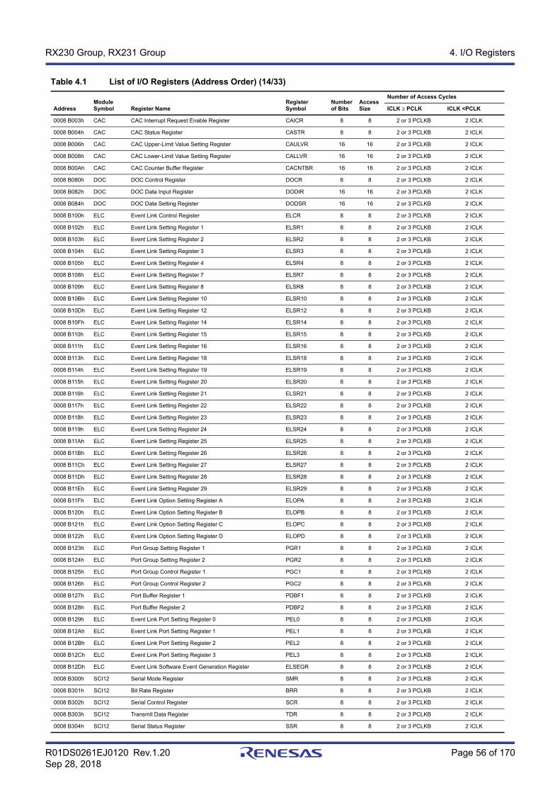
R01DS0261EJ0120 Rev.1.20 Page 56 of 170Sep 28, 2018
RX230 Group, RX231 Group 4. I/O Registers
0008 B003h CAC CAC Interrupt Request Enable Register CAICR 8 8 2 or 3 PCLKB 2 ICLK
0008 B004h CAC CAC Status Register CASTR 8 8 2 or 3 PCLKB 2 ICLK
0008 B006h CAC CAC Upper-Limit Value Setting Register CAULVR 16 16 2 or 3 PCLKB 2 ICLK
0008 B008h CAC CAC Lower-Limit Value Setting Register CALLVR 16 16 2 or 3 PCLKB 2 ICLK
0008 B00Ah CAC CAC Counter Buffer Register CACNTBR 16 16 2 or 3 PCLKB 2 ICLK
0008 B080h DOC DOC Control Register DOCR 8 8 2 or 3 PCLKB 2 ICLK
0008 B082h DOC DOC Data Input Register DODIR 16 16 2 or 3 PCLKB 2 ICLK
0008 B084h DOC DOC Data Setting Register DODSR 16 16 2 or 3 PCLKB 2 ICLK
0008 B100h ELC Event Link Control Register ELCR 8 8 2 or 3 PCLKB 2 ICLK
0008 B102h ELC Event Link Setting Register 1 ELSR1 8 8 2 or 3 PCLKB 2 ICLK
0008 B103h ELC Event Link Setting Register 2 ELSR2 8 8 2 or 3 PCLKB 2 ICLK
0008 B104h ELC Event Link Setting Register 3 ELSR3 8 8 2 or 3 PCLKB 2 ICLK
0008 B105h ELC Event Link Setting Register 4 ELSR4 8 8 2 or 3 PCLKB 2 ICLK
0008 B108h ELC Event Link Setting Register 7 ELSR7 8 8 2 or 3 PCLKB 2 ICLK
0008 B109h ELC Event Link Setting Register 8 ELSR8 8 8 2 or 3 PCLKB 2 ICLK
0008 B10Bh ELC Event Link Setting Register 10 ELSR10 8 8 2 or 3 PCLKB 2 ICLK
0008 B10Dh ELC Event Link Setting Register 12 ELSR12 8 8 2 or 3 PCLKB 2 ICLK
0008 B10Fh ELC Event Link Setting Register 14 ELSR14 8 8 2 or 3 PCLKB 2 ICLK
0008 B110h ELC Event Link Setting Register 15 ELSR15 8 8 2 or 3 PCLKB 2 ICLK
0008 B111h ELC Event Link Setting Register 16 ELSR16 8 8 2 or 3 PCLKB 2 ICLK
0008 B113h ELC Event Link Setting Register 18 ELSR18 8 8 2 or 3 PCLKB 2 ICLK
0008 B114h ELC Event Link Setting Register 19 ELSR19 8 8 2 or 3 PCLKB 2 ICLK
0008 B115h ELC Event Link Setting Register 20 ELSR20 8 8 2 or 3 PCLKB 2 ICLK
0008 B116h ELC Event Link Setting Register 21 ELSR21 8 8 2 or 3 PCLKB 2 ICLK
0008 B117h ELC Event Link Setting Register 22 ELSR22 8 8 2 or 3 PCLKB 2 ICLK
0008 B118h ELC Event Link Setting Register 23 ELSR23 8 8 2 or 3 PCLKB 2 ICLK
0008 B119h ELC Event Link Setting Register 24 ELSR24 8 8 2 or 3 PCLKB 2 ICLK
0008 B11Ah ELC Event Link Setting Register 25 ELSR25 8 8 2 or 3 PCLKB 2 ICLK
0008 B11Bh ELC Event Link Setting Register 26 ELSR26 8 8 2 or 3 PCLKB 2 ICLK
0008 B11Ch ELC Event Link Setting Register 27 ELSR27 8 8 2 or 3 PCLKB 2 ICLK
0008 B11Dh ELC Event Link Setting Register 28 ELSR28 8 8 2 or 3 PCLKB 2 ICLK
0008 B11Eh ELC Event Link Setting Register 29 ELSR29 8 8 2 or 3 PCLKB 2 ICLK
0008 B11Fh ELC Event Link Option Setting Register A ELOPA 8 8 2 or 3 PCLKB 2 ICLK
0008 B120h ELC Event Link Option Setting Register B ELOPB 8 8 2 or 3 PCLKB 2 ICLK
0008 B121h ELC Event Link Option Setting Register C ELOPC 8 8 2 or 3 PCLKB 2 ICLK
0008 B122h ELC Event Link Option Setting Register D ELOPD 8 8 2 or 3 PCLKB 2 ICLK
0008 B123h ELC Port Group Setting Register 1 PGR1 8 8 2 or 3 PCLKB 2 ICLK
0008 B124h ELC Port Group Setting Register 2 PGR2 8 8 2 or 3 PCLKB 2 ICLK
0008 B125h ELC Port Group Control Register 1 PGC1 8 8 2 or 3 PCLKB 2 ICLK
0008 B126h ELC Port Group Control Register 2 PGC2 8 8 2 or 3 PCLKB 2 ICLK
0008 B127h ELC Port Buffer Register 1 PDBF1 8 8 2 or 3 PCLKB 2 ICLK
0008 B128h ELC Port Buffer Register 2 PDBF2 8 8 2 or 3 PCLKB 2 ICLK
0008 B129h ELC Event Link Port Setting Register 0 PEL0 8 8 2 or 3 PCLKB 2 ICLK
0008 B12Ah ELC Event Link Port Setting Register 1 PEL1 8 8 2 or 3 PCLKB 2 ICLK
0008 B12Bh ELC Event Link Port Setting Register 2 PEL2 8 8 2 or 3 PCLKB 2 ICLK
0008 B12Ch ELC Event Link Port Setting Register 3 PEL3 8 8 2 or 3 PCLKB 2 ICLK
0008 B12Dh ELC Event Link Software Event Generation Register ELSEGR 8 8 2 or 3 PCLKB 2 ICLK
0008 B300h SCI12 Serial Mode Register SMR 8 8 2 or 3 PCLKB 2 ICLK
0008 B301h SCI12 Bit Rate Register BRR 8 8 2 or 3 PCLKB 2 ICLK
0008 B302h SCI12 Serial Control Register SCR 8 8 2 or 3 PCLKB 2 ICLK
0008 B303h SCI12 Transmit Data Register TDR 8 8 2 or 3 PCLKB 2 ICLK
0008 B304h SCI12 Serial Status Register SSR 8 8 2 or 3 PCLKB 2 ICLK
Table 4.1 List of I/O Registers (Address Order) (14/33)
AddressModule Symbol Register Name
Register Symbol
Number of Bits
Access Size
Number of Access Cycles
ICLK ≥ PCLK ICLK <PCLK
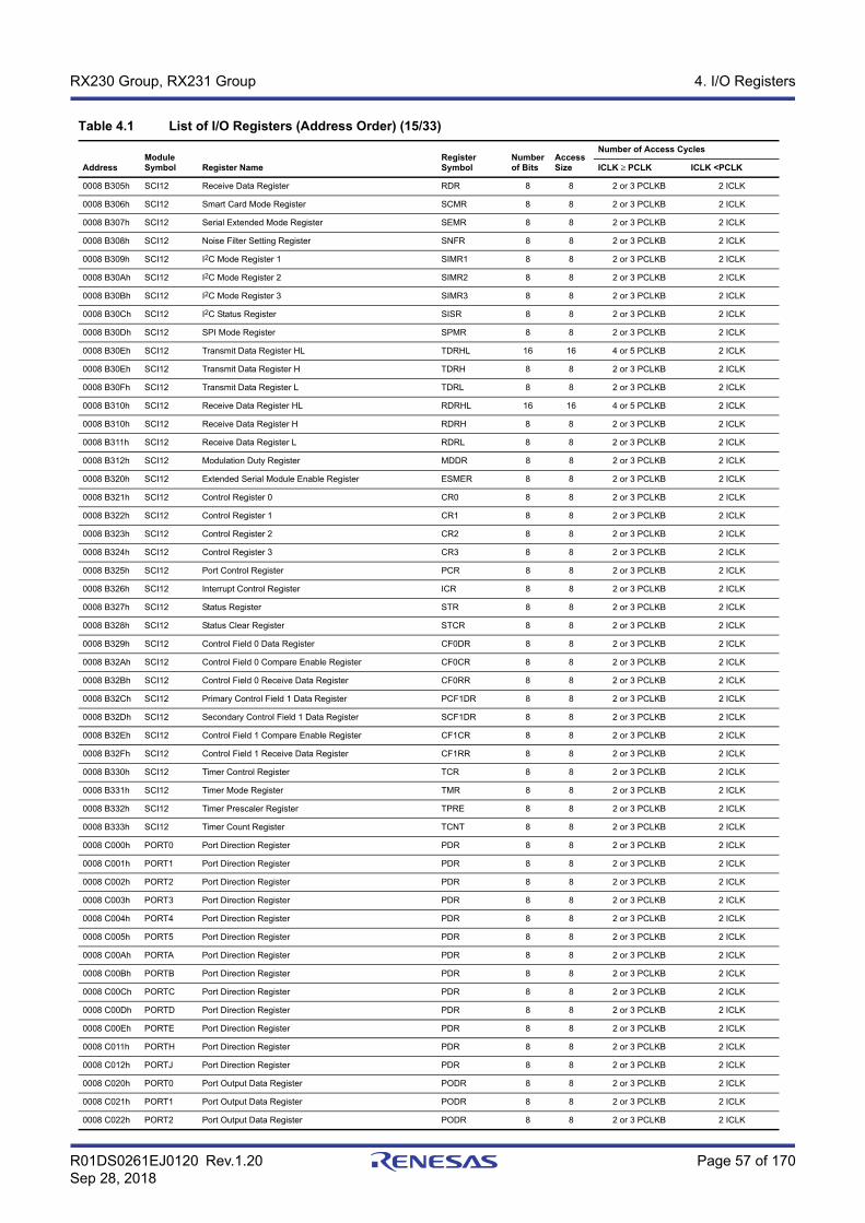
R01DS0261EJ0120 Rev.1.20 Page 57 of 170Sep 28, 2018
RX230 Group, RX231 Group 4. I/O Registers
0008 B305h SCI12 Receive Data Register RDR 8 8 2 or 3 PCLKB 2 ICLK
0008 B306h SCI12 Smart Card Mode Register SCMR 8 8 2 or 3 PCLKB 2 ICLK
0008 B307h SCI12 Serial Extended Mode Register SEMR 8 8 2 or 3 PCLKB 2 ICLK
0008 B308h SCI12 Noise Filter Setting Register SNFR 8 8 2 or 3 PCLKB 2 ICLK
0008 B309h SCI12 I2C Mode Register 1 SIMR1 8 8 2 or 3 PCLKB 2 ICLK
0008 B30Ah SCI12 I2C Mode Register 2 SIMR2 8 8 2 or 3 PCLKB 2 ICLK
0008 B30Bh SCI12 I2C Mode Register 3 SIMR3 8 8 2 or 3 PCLKB 2 ICLK
0008 B30Ch SCI12 I2C Status Register SISR 8 8 2 or 3 PCLKB 2 ICLK
0008 B30Dh SCI12 SPI Mode Register SPMR 8 8 2 or 3 PCLKB 2 ICLK
0008 B30Eh SCI12 Transmit Data Register HL TDRHL 16 16 4 or 5 PCLKB 2 ICLK
0008 B30Eh SCI12 Transmit Data Register H TDRH 8 8 2 or 3 PCLKB 2 ICLK
0008 B30Fh SCI12 Transmit Data Register L TDRL 8 8 2 or 3 PCLKB 2 ICLK
0008 B310h SCI12 Receive Data Register HL RDRHL 16 16 4 or 5 PCLKB 2 ICLK
0008 B310h SCI12 Receive Data Register H RDRH 8 8 2 or 3 PCLKB 2 ICLK
0008 B311h SCI12 Receive Data Register L RDRL 8 8 2 or 3 PCLKB 2 ICLK
0008 B312h SCI12 Modulation Duty Register MDDR 8 8 2 or 3 PCLKB 2 ICLK
0008 B320h SCI12 Extended Serial Module Enable Register ESMER 8 8 2 or 3 PCLKB 2 ICLK
0008 B321h SCI12 Control Register 0 CR0 8 8 2 or 3 PCLKB 2 ICLK
0008 B322h SCI12 Control Register 1 CR1 8 8 2 or 3 PCLKB 2 ICLK
0008 B323h SCI12 Control Register 2 CR2 8 8 2 or 3 PCLKB 2 ICLK
0008 B324h SCI12 Control Register 3 CR3 8 8 2 or 3 PCLKB 2 ICLK
0008 B325h SCI12 Port Control Register PCR 8 8 2 or 3 PCLKB 2 ICLK
0008 B326h SCI12 Interrupt Control Register ICR 8 8 2 or 3 PCLKB 2 ICLK
0008 B327h SCI12 Status Register STR 8 8 2 or 3 PCLKB 2 ICLK
0008 B328h SCI12 Status Clear Register STCR 8 8 2 or 3 PCLKB 2 ICLK
0008 B329h SCI12 Control Field 0 Data Register CF0DR 8 8 2 or 3 PCLKB 2 ICLK
0008 B32Ah SCI12 Control Field 0 Compare Enable Register CF0CR 8 8 2 or 3 PCLKB 2 ICLK
0008 B32Bh SCI12 Control Field 0 Receive Data Register CF0RR 8 8 2 or 3 PCLKB 2 ICLK
0008 B32Ch SCI12 Primary Control Field 1 Data Register PCF1DR 8 8 2 or 3 PCLKB 2 ICLK
0008 B32Dh SCI12 Secondary Control Field 1 Data Register SCF1DR 8 8 2 or 3 PCLKB 2 ICLK
0008 B32Eh SCI12 Control Field 1 Compare Enable Register CF1CR 8 8 2 or 3 PCLKB 2 ICLK
0008 B32Fh SCI12 Control Field 1 Receive Data Register CF1RR 8 8 2 or 3 PCLKB 2 ICLK
0008 B330h SCI12 Timer Control Register TCR 8 8 2 or 3 PCLKB 2 ICLK
0008 B331h SCI12 Timer Mode Register TMR 8 8 2 or 3 PCLKB 2 ICLK
0008 B332h SCI12 Timer Prescaler Register TPRE 8 8 2 or 3 PCLKB 2 ICLK
0008 B333h SCI12 Timer Count Register TCNT 8 8 2 or 3 PCLKB 2 ICLK
0008 C000h PORT0 Port Direction Register PDR 8 8 2 or 3 PCLKB 2 ICLK
0008 C001h PORT1 Port Direction Register PDR 8 8 2 or 3 PCLKB 2 ICLK
0008 C002h PORT2 Port Direction Register PDR 8 8 2 or 3 PCLKB 2 ICLK
0008 C003h PORT3 Port Direction Register PDR 8 8 2 or 3 PCLKB 2 ICLK
0008 C004h PORT4 Port Direction Register PDR 8 8 2 or 3 PCLKB 2 ICLK
0008 C005h PORT5 Port Direction Register PDR 8 8 2 or 3 PCLKB 2 ICLK
0008 C00Ah PORTA Port Direction Register PDR 8 8 2 or 3 PCLKB 2 ICLK
0008 C00Bh PORTB Port Direction Register PDR 8 8 2 or 3 PCLKB 2 ICLK
0008 C00Ch PORTC Port Direction Register PDR 8 8 2 or 3 PCLKB 2 ICLK
0008 C00Dh PORTD Port Direction Register PDR 8 8 2 or 3 PCLKB 2 ICLK
0008 C00Eh PORTE Port Direction Register PDR 8 8 2 or 3 PCLKB 2 ICLK
0008 C011h PORTH Port Direction Register PDR 8 8 2 or 3 PCLKB 2 ICLK
0008 C012h PORTJ Port Direction Register PDR 8 8 2 or 3 PCLKB 2 ICLK
0008 C020h PORT0 Port Output Data Register PODR 8 8 2 or 3 PCLKB 2 ICLK
0008 C021h PORT1 Port Output Data Register PODR 8 8 2 or 3 PCLKB 2 ICLK
0008 C022h PORT2 Port Output Data Register PODR 8 8 2 or 3 PCLKB 2 ICLK
Table 4.1 List of I/O Registers (Address Order) (15/33)
AddressModule Symbol Register Name
Register Symbol
Number of Bits
Access Size
Number of Access Cycles
ICLK ≥ PCLK ICLK <PCLK

R01DS0261EJ0120 Rev.1.20 Page 58 of 170Sep 28, 2018
RX230 Group, RX231 Group 4. I/O Registers
0008 C023h PORT3 Port Output Data Register PODR 8 8 2 or 3 PCLKB 2 ICLK
0008 C024h PORT4 Port Output Data Register PODR 8 8 2 or 3 PCLKB 2 ICLK
0008 C025h PORT5 Port Output Data Register PODR 8 8 2 or 3 PCLKB 2 ICLK
0008 C02Ah PORTA Port Output Data Register PODR 8 8 2 or 3 PCLKB 2 ICLK
0008 C02Bh PORTB Port Output Data Register PODR 8 8 2 or 3 PCLKB 2 ICLK
0008 C02Ch PORTC Port Output Data Register PODR 8 8 2 or 3 PCLKB 2 ICLK
0008 C02Dh PORTD Port Output Data Register PODR 8 8 2 or 3 PCLKB 2 ICLK
0008 C02Eh PORTE Port Output Data Register PODR 8 8 2 or 3 PCLKB 2 ICLK
0008 C031h PORTH Port Output Data Register PODR 8 8 2 or 3 PCLKB 2 ICLK
0008 C032h PORTJ Port Output Data Register PODR 8 8 2 or 3 PCLKB 2 ICLK
0008 C040h PORT0 Port Input Data Register PIDR 8 8 3 or 4 PCLKB 3 ICLK
0008 C041h PORT1 Port Input Data Register PIDR 8 8 3 or 4 PCLKB 3 ICLK
0008 C042h PORT2 Port Input Data Register PIDR 8 8 3 or 4 PCLKB 3 ICLK
0008 C043h PORT3 Port Input Data Register PIDR 8 8 3 or 4 PCLKB 3 ICLK
0008 C044h PORT4 Port Input Data Register PIDR 8 8 3 or 4 PCLKB 3 ICLK
0008 C045h PORT5 Port Input Data Register PIDR 8 8 3 or 4 PCLKB 3 ICLK
0008 C04Ah PORTA Port Input Data Register PIDR 8 8 3 or 4 PCLKB 3 ICLK
0008 C04Bh PORTB Port Input Data Register PIDR 8 8 3 or 4 PCLKB 3 ICLK
0008 C04Ch PORTC Port Input Data Register PIDR 8 8 3 or 4 PCLKB 3 ICLK
0008 C04Dh PORTD Port Input Data Register PIDR 8 8 3 or 4 PCLKB 3 ICLK
0008 C04Eh PORTE Port Input Data Register PIDR 8 8 3 or 4 PCLKB 3 ICLK
0008 C051h PORTH Port Input Data Register PIDR 8 8 3 or 4 PCLKB 3 ICLK
0008 C052h PORTJ Port Input Data Register PIDR 8 8 3 or 4 PCLKB 3 ICLK
0008 C060h PORT0 Port Mode Register PMR 8 8 2 or 3 PCLKB 2 ICLK
0008 C061h PORT1 Port Mode Register PMR 8 8 2 or 3 PCLKB 2 ICLK
0008 C062h PORT2 Port Mode Register PMR 8 8 2 or 3 PCLKB 2 ICLK
0008 C063h PORT3 Port Mode Register PMR 8 8 2 or 3 PCLKB 2 ICLK
0008 C064h PORT4 Port Mode Register PMR 8 8 2 or 3 PCLKB 2 ICLK
0008 C065h PORT5 Port Mode Register PMR 8 8 2 or 3 PCLKB 2 ICLK
0008 C06Ah PORTA Port Mode Register PMR 8 8 2 or 3 PCLKB 2 ICLK
0008 C06Bh PORTB Port Mode Register PMR 8 8 2 or 3 PCLKB 2 ICLK
0008 C06Ch PORTC Port Mode Register PMR 8 8 2 or 3 PCLKB 2 ICLK
0008 C06Dh PORTD Port Mode Register PMR 8 8 2 or 3 PCLKB 2 ICLK
0008 C06Eh PORTE Port Mode Register PMR 8 8 2 or 3 PCLKB 2 ICLK
0008 C071h PORTH Port Mode Register PMR 8 8 2 or 3 PCLKB 2 ICLK
0008 C072h PORTJ Port Mode Register PMR 8 8 2 or 3 PCLKB 2 ICLK
0008 C082h PORT1 Open Drain Control Register 0 ODR0 8 8, 16 2 or 3 PCLKB 2 ICLK
0008 C083h PORT1 Open Drain Control Register 1 ODR1 8 8, 16 2 or 3 PCLKB 2 ICLK
0008 C084h PORT2 Open Drain Control Register 0 ODR0 8 8, 16 2 or 3 PCLKB 2 ICLK
0008 C085h PORT2 Open Drain Control Register 1 ODR1 8 8, 16 2 or 3 PCLKB 2 ICLK
0008 C086h PORT3 Open Drain Control Register 0 ODR0 8 8, 16 2 or 3 PCLKB 2 ICLK
0008 C087h PORT3 Open Drain Control Register 1 ODR1 8 8, 16 2 or 3 PCLKB 2 ICLK
0008 C08Ah PORT5 Open Drain Control Register 0 ODR0 8 8, 16 2 or 3 PCLKB 2 ICLK
0008 C08Bh PORT5 Open Drain Control Register 1 ODR1 8 8, 16 2 or 3 PCLKB 2 ICLK
0008 C094h PORTA Open Drain Control Register 0 ODR0 8 8, 16 2 or 3 PCLKB 2 ICLK
0008 C095h PORTA Open Drain Control Register 1 ODR1 8 8, 16 2 or 3 PCLKB 2 ICLK
0008 C096h PORTB Open Drain Control Register 0 ODR0 8 8, 16 2 or 3 PCLKB 2 ICLK
0008 C097h PORTB Open Drain Control Register 1 ODR1 8 8, 16 2 or 3 PCLKB 2 ICLK
0008 C098h PORTC Open Drain Control Register 0 ODR0 8 8, 16 2 or 3 PCLKB 2 ICLK
0008 C099h PORTC Open Drain Control Register 1 ODR1 8 8, 16 2 or 3 PCLKB 2 ICLK
0008 C09Ch PORTE Open Drain Control Register 0 ODR0 8 8, 16 2 or 3 PCLKB 2 ICLK
0008 C09Dh PORTE Open Drain Control Register 1 ODR1 8 8, 16 2 or 3 PCLKB 2 ICLK
Table 4.1 List of I/O Registers (Address Order) (16/33)
AddressModule Symbol Register Name
Register Symbol
Number of Bits
Access Size
Number of Access Cycles
ICLK ≥ PCLK ICLK <PCLK
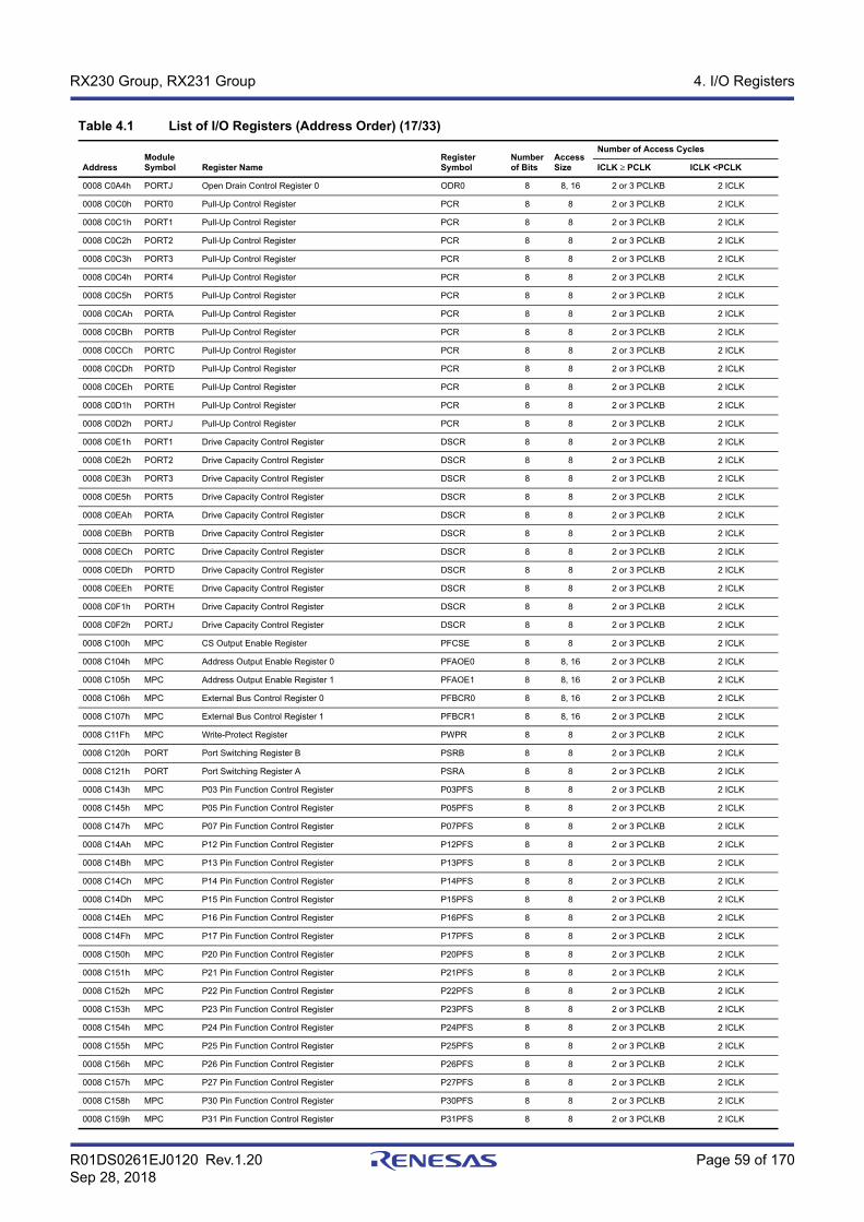
R01DS0261EJ0120 Rev.1.20 Page 59 of 170Sep 28, 2018
RX230 Group, RX231 Group 4. I/O Registers
0008 C0A4h PORTJ Open Drain Control Register 0 ODR0 8 8, 16 2 or 3 PCLKB 2 ICLK
0008 C0C0h PORT0 Pull-Up Control Register PCR 8 8 2 or 3 PCLKB 2 ICLK
0008 C0C1h PORT1 Pull-Up Control Register PCR 8 8 2 or 3 PCLKB 2 ICLK
0008 C0C2h PORT2 Pull-Up Control Register PCR 8 8 2 or 3 PCLKB 2 ICLK
0008 C0C3h PORT3 Pull-Up Control Register PCR 8 8 2 or 3 PCLKB 2 ICLK
0008 C0C4h PORT4 Pull-Up Control Register PCR 8 8 2 or 3 PCLKB 2 ICLK
0008 C0C5h PORT5 Pull-Up Control Register PCR 8 8 2 or 3 PCLKB 2 ICLK
0008 C0CAh PORTA Pull-Up Control Register PCR 8 8 2 or 3 PCLKB 2 ICLK
0008 C0CBh PORTB Pull-Up Control Register PCR 8 8 2 or 3 PCLKB 2 ICLK
0008 C0CCh PORTC Pull-Up Control Register PCR 8 8 2 or 3 PCLKB 2 ICLK
0008 C0CDh PORTD Pull-Up Control Register PCR 8 8 2 or 3 PCLKB 2 ICLK
0008 C0CEh PORTE Pull-Up Control Register PCR 8 8 2 or 3 PCLKB 2 ICLK
0008 C0D1h PORTH Pull-Up Control Register PCR 8 8 2 or 3 PCLKB 2 ICLK
0008 C0D2h PORTJ Pull-Up Control Register PCR 8 8 2 or 3 PCLKB 2 ICLK
0008 C0E1h PORT1 Drive Capacity Control Register DSCR 8 8 2 or 3 PCLKB 2 ICLK
0008 C0E2h PORT2 Drive Capacity Control Register DSCR 8 8 2 or 3 PCLKB 2 ICLK
0008 C0E3h PORT3 Drive Capacity Control Register DSCR 8 8 2 or 3 PCLKB 2 ICLK
0008 C0E5h PORT5 Drive Capacity Control Register DSCR 8 8 2 or 3 PCLKB 2 ICLK
0008 C0EAh PORTA Drive Capacity Control Register DSCR 8 8 2 or 3 PCLKB 2 ICLK
0008 C0EBh PORTB Drive Capacity Control Register DSCR 8 8 2 or 3 PCLKB 2 ICLK
0008 C0ECh PORTC Drive Capacity Control Register DSCR 8 8 2 or 3 PCLKB 2 ICLK
0008 C0EDh PORTD Drive Capacity Control Register DSCR 8 8 2 or 3 PCLKB 2 ICLK
0008 C0EEh PORTE Drive Capacity Control Register DSCR 8 8 2 or 3 PCLKB 2 ICLK
0008 C0F1h PORTH Drive Capacity Control Register DSCR 8 8 2 or 3 PCLKB 2 ICLK
0008 C0F2h PORTJ Drive Capacity Control Register DSCR 8 8 2 or 3 PCLKB 2 ICLK
0008 C100h MPC CS Output Enable Register PFCSE 8 8 2 or 3 PCLKB 2 ICLK
0008 C104h MPC Address Output Enable Register 0 PFAOE0 8 8, 16 2 or 3 PCLKB 2 ICLK
0008 C105h MPC Address Output Enable Register 1 PFAOE1 8 8, 16 2 or 3 PCLKB 2 ICLK
0008 C106h MPC External Bus Control Register 0 PFBCR0 8 8, 16 2 or 3 PCLKB 2 ICLK
0008 C107h MPC External Bus Control Register 1 PFBCR1 8 8, 16 2 or 3 PCLKB 2 ICLK
0008 C11Fh MPC Write-Protect Register PWPR 8 8 2 or 3 PCLKB 2 ICLK
0008 C120h PORT Port Switching Register B PSRB 8 8 2 or 3 PCLKB 2 ICLK
0008 C121h PORT Port Switching Register A PSRA 8 8 2 or 3 PCLKB 2 ICLK
0008 C143h MPC P03 Pin Function Control Register P03PFS 8 8 2 or 3 PCLKB 2 ICLK
0008 C145h MPC P05 Pin Function Control Register P05PFS 8 8 2 or 3 PCLKB 2 ICLK
0008 C147h MPC P07 Pin Function Control Register P07PFS 8 8 2 or 3 PCLKB 2 ICLK
0008 C14Ah MPC P12 Pin Function Control Register P12PFS 8 8 2 or 3 PCLKB 2 ICLK
0008 C14Bh MPC P13 Pin Function Control Register P13PFS 8 8 2 or 3 PCLKB 2 ICLK
0008 C14Ch MPC P14 Pin Function Control Register P14PFS 8 8 2 or 3 PCLKB 2 ICLK
0008 C14Dh MPC P15 Pin Function Control Register P15PFS 8 8 2 or 3 PCLKB 2 ICLK
0008 C14Eh MPC P16 Pin Function Control Register P16PFS 8 8 2 or 3 PCLKB 2 ICLK
0008 C14Fh MPC P17 Pin Function Control Register P17PFS 8 8 2 or 3 PCLKB 2 ICLK
0008 C150h MPC P20 Pin Function Control Register P20PFS 8 8 2 or 3 PCLKB 2 ICLK
0008 C151h MPC P21 Pin Function Control Register P21PFS 8 8 2 or 3 PCLKB 2 ICLK
0008 C152h MPC P22 Pin Function Control Register P22PFS 8 8 2 or 3 PCLKB 2 ICLK
0008 C153h MPC P23 Pin Function Control Register P23PFS 8 8 2 or 3 PCLKB 2 ICLK
0008 C154h MPC P24 Pin Function Control Register P24PFS 8 8 2 or 3 PCLKB 2 ICLK
0008 C155h MPC P25 Pin Function Control Register P25PFS 8 8 2 or 3 PCLKB 2 ICLK
0008 C156h MPC P26 Pin Function Control Register P26PFS 8 8 2 or 3 PCLKB 2 ICLK
0008 C157h MPC P27 Pin Function Control Register P27PFS 8 8 2 or 3 PCLKB 2 ICLK
0008 C158h MPC P30 Pin Function Control Register P30PFS 8 8 2 or 3 PCLKB 2 ICLK
0008 C159h MPC P31 Pin Function Control Register P31PFS 8 8 2 or 3 PCLKB 2 ICLK
Table 4.1 List of I/O Registers (Address Order) (17/33)
AddressModule Symbol Register Name
Register Symbol
Number of Bits
Access Size
Number of Access Cycles
ICLK ≥ PCLK ICLK <PCLK
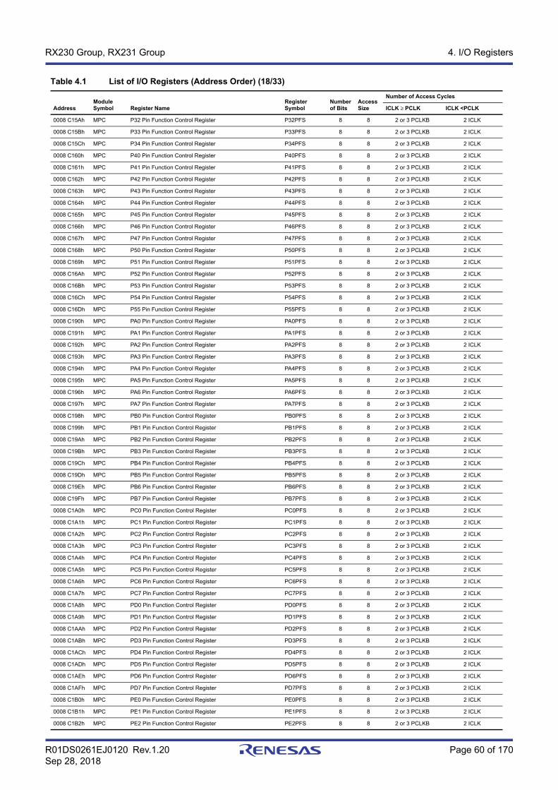
R01DS0261EJ0120 Rev.1.20 Page 60 of 170Sep 28, 2018
RX230 Group, RX231 Group 4. I/O Registers
0008 C15Ah MPC P32 Pin Function Control Register P32PFS 8 8 2 or 3 PCLKB 2 ICLK
0008 C15Bh MPC P33 Pin Function Control Register P33PFS 8 8 2 or 3 PCLKB 2 ICLK
0008 C15Ch MPC P34 Pin Function Control Register P34PFS 8 8 2 or 3 PCLKB 2 ICLK
0008 C160h MPC P40 Pin Function Control Register P40PFS 8 8 2 or 3 PCLKB 2 ICLK
0008 C161h MPC P41 Pin Function Control Register P41PFS 8 8 2 or 3 PCLKB 2 ICLK
0008 C162h MPC P42 Pin Function Control Register P42PFS 8 8 2 or 3 PCLKB 2 ICLK
0008 C163h MPC P43 Pin Function Control Register P43PFS 8 8 2 or 3 PCLKB 2 ICLK
0008 C164h MPC P44 Pin Function Control Register P44PFS 8 8 2 or 3 PCLKB 2 ICLK
0008 C165h MPC P45 Pin Function Control Register P45PFS 8 8 2 or 3 PCLKB 2 ICLK
0008 C166h MPC P46 Pin Function Control Register P46PFS 8 8 2 or 3 PCLKB 2 ICLK
0008 C167h MPC P47 Pin Function Control Register P47PFS 8 8 2 or 3 PCLKB 2 ICLK
0008 C168h MPC P50 Pin Function Control Register P50PFS 8 8 2 or 3 PCLKB 2 ICLK
0008 C169h MPC P51 Pin Function Control Register P51PFS 8 8 2 or 3 PCLKB 2 ICLK
0008 C16Ah MPC P52 Pin Function Control Register P52PFS 8 8 2 or 3 PCLKB 2 ICLK
0008 C16Bh MPC P53 Pin Function Control Register P53PFS 8 8 2 or 3 PCLKB 2 ICLK
0008 C16Ch MPC P54 Pin Function Control Register P54PFS 8 8 2 or 3 PCLKB 2 ICLK
0008 C16Dh MPC P55 Pin Function Control Register P55PFS 8 8 2 or 3 PCLKB 2 ICLK
0008 C190h MPC PA0 Pin Function Control Register PA0PFS 8 8 2 or 3 PCLKB 2 ICLK
0008 C191h MPC PA1 Pin Function Control Register PA1PFS 8 8 2 or 3 PCLKB 2 ICLK
0008 C192h MPC PA2 Pin Function Control Register PA2PFS 8 8 2 or 3 PCLKB 2 ICLK
0008 C193h MPC PA3 Pin Function Control Register PA3PFS 8 8 2 or 3 PCLKB 2 ICLK
0008 C194h MPC PA4 Pin Function Control Register PA4PFS 8 8 2 or 3 PCLKB 2 ICLK
0008 C195h MPC PA5 Pin Function Control Register PA5PFS 8 8 2 or 3 PCLKB 2 ICLK
0008 C196h MPC PA6 Pin Function Control Register PA6PFS 8 8 2 or 3 PCLKB 2 ICLK
0008 C197h MPC PA7 Pin Function Control Register PA7PFS 8 8 2 or 3 PCLKB 2 ICLK
0008 C198h MPC PB0 Pin Function Control Register PB0PFS 8 8 2 or 3 PCLKB 2 ICLK
0008 C199h MPC PB1 Pin Function Control Register PB1PFS 8 8 2 or 3 PCLKB 2 ICLK
0008 C19Ah MPC PB2 Pin Function Control Register PB2PFS 8 8 2 or 3 PCLKB 2 ICLK
0008 C19Bh MPC PB3 Pin Function Control Register PB3PFS 8 8 2 or 3 PCLKB 2 ICLK
0008 C19Ch MPC PB4 Pin Function Control Register PB4PFS 8 8 2 or 3 PCLKB 2 ICLK
0008 C19Dh MPC PB5 Pin Function Control Register PB5PFS 8 8 2 or 3 PCLKB 2 ICLK
0008 C19Eh MPC PB6 Pin Function Control Register PB6PFS 8 8 2 or 3 PCLKB 2 ICLK
0008 C19Fh MPC PB7 Pin Function Control Register PB7PFS 8 8 2 or 3 PCLKB 2 ICLK
0008 C1A0h MPC PC0 Pin Function Control Register PC0PFS 8 8 2 or 3 PCLKB 2 ICLK
0008 C1A1h MPC PC1 Pin Function Control Register PC1PFS 8 8 2 or 3 PCLKB 2 ICLK
0008 C1A2h MPC PC2 Pin Function Control Register PC2PFS 8 8 2 or 3 PCLKB 2 ICLK
0008 C1A3h MPC PC3 Pin Function Control Register PC3PFS 8 8 2 or 3 PCLKB 2 ICLK
0008 C1A4h MPC PC4 Pin Function Control Register PC4PFS 8 8 2 or 3 PCLKB 2 ICLK
0008 C1A5h MPC PC5 Pin Function Control Register PC5PFS 8 8 2 or 3 PCLKB 2 ICLK
0008 C1A6h MPC PC6 Pin Function Control Register PC6PFS 8 8 2 or 3 PCLKB 2 ICLK
0008 C1A7h MPC PC7 Pin Function Control Register PC7PFS 8 8 2 or 3 PCLKB 2 ICLK
0008 C1A8h MPC PD0 Pin Function Control Register PD0PFS 8 8 2 or 3 PCLKB 2 ICLK
0008 C1A9h MPC PD1 Pin Function Control Register PD1PFS 8 8 2 or 3 PCLKB 2 ICLK
0008 C1AAh MPC PD2 Pin Function Control Register PD2PFS 8 8 2 or 3 PCLKB 2 ICLK
0008 C1ABh MPC PD3 Pin Function Control Register PD3PFS 8 8 2 or 3 PCLKB 2 ICLK
0008 C1ACh MPC PD4 Pin Function Control Register PD4PFS 8 8 2 or 3 PCLKB 2 ICLK
0008 C1ADh MPC PD5 Pin Function Control Register PD5PFS 8 8 2 or 3 PCLKB 2 ICLK
0008 C1AEh MPC PD6 Pin Function Control Register PD6PFS 8 8 2 or 3 PCLKB 2 ICLK
0008 C1AFh MPC PD7 Pin Function Control Register PD7PFS 8 8 2 or 3 PCLKB 2 ICLK
0008 C1B0h MPC PE0 Pin Function Control Register PE0PFS 8 8 2 or 3 PCLKB 2 ICLK
0008 C1B1h MPC PE1 Pin Function Control Register PE1PFS 8 8 2 or 3 PCLKB 2 ICLK
0008 C1B2h MPC PE2 Pin Function Control Register PE2PFS 8 8 2 or 3 PCLKB 2 ICLK
Table 4.1 List of I/O Registers (Address Order) (18/33)
AddressModule Symbol Register Name
Register Symbol
Number of Bits
Access Size
Number of Access Cycles
ICLK ≥ PCLK ICLK <PCLK
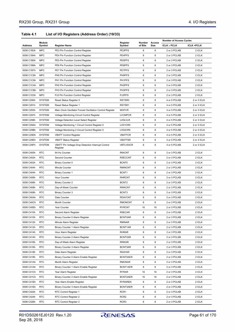
R01DS0261EJ0120 Rev.1.20 Page 61 of 170Sep 28, 2018
RX230 Group, RX231 Group 4. I/O Registers
0008 C1B3h MPC PE3 Pin Function Control Register PE3PFS 8 8 2 or 3 PCLKB 2 ICLK
0008 C1B4h MPC PE4 Pin Function Control Register PE4PFS 8 8 2 or 3 PCLKB 2 ICLK
0008 C1B5h MPC PE5 Pin Function Control Register PE5PFS 8 8 2 or 3 PCLKB 2 ICLK
0008 C1B6h MPC PE6 Pin Function Control Register PE6PFS 8 8 2 or 3 PCLKB 2 ICLK
0008 C1B7h MPC PE7 Pin Function Control Register PE7PFS 8 8 2 or 3 PCLKB 2 ICLK
0008 C1C8h MPC PH0 Pin Function Control Register PH0PFS 8 8 2 or 3 PCLKB 2 ICLK
0008 C1C9h MPC PH1 Pin Function Control Register PH1PFS 8 8 2 or 3 PCLKB 2 ICLK
0008 C1CAh MPC PH2 Pin Function Control Register PH2PFS 8 8 2 or 3 PCLKB 2 ICLK
0008 C1CBh MPC PH3 Pin Function Control Register PH3PFS 8 8 2 or 3 PCLKB 2 ICLK
0008 C1D3h MPC PJ3 Pin Function Control Register PJ3PFS 8 8 2 or 3 PCLKB 2 ICLK
0008 C290h SYSTEM Reset Status Register 0 RSTSR0 8 8 4 or 5 PCLKB 2 or 3 ICLK
0008 C291h SYSTEM Reset Status Register 1 RSTSR1 8 8 4 or 5 PCLKB 2 or 3 ICLK
0008 C293h SYSTEM Main Clock Oscillator Forced Oscillation Control Register MOFCR 8 8 4 or 5 PCLKB 2 or 3 ICLK
0008 C297h SYSTEM Voltage Monitoring Circuit Control Register LVCMPCR 8 8 4 or 5 PCLKB 2 or 3 ICLK
0008 C298h SYSTEM Voltage Detection Level Select Register LVDLVLR 8 8 4 or 5 PCLKB 2 or 3 ICLK
0008 C29Ah SYSTEM Voltage Monitoring 1 Circuit Control Register 0 LVD1CR0 8 8 4 or 5 PCLKB 2 or 3 ICLK
0008 C29Bh SYSTEM Voltage Monitoring 2 Circuit Control Register 0 LVD2CR0 8 8 4 or 5 PCLKB 2 or 3 ICLK
0008 C29Dh SYSTEM VBATT Control Register VBATTCR 8 8 4 or 5 PCLKB 2 or 3 ICLK
0008 C29Eh SYSTEM VBATT Status Register VBATTSR 8 8 4 or 5 PCLKB 2 or 3 ICLK
0008 C29Fh SYSTEM VBATT Pin Voltage Drop Detection Interrupt Control Register
VBTLVDICR 8 8 4 or 5 PCLKB 2 or 3 ICLK
0008 C400h RTC 64-Hz Counter R64CNT 8 8 2 or 3 PCLKB 2 ICLK
0008 C402h RTC Second Counter RSECCNT 8 8 2 or 3 PCLKB 2 ICLK
0008 C402h RTC Binary Counter 0 BCNT0 8 8 2 or 3 PCLKB 2 ICLK
0008 C404h RTC Minute Counter RMINCNT 8 8 2 or 3 PCLKB 2 ICLK
0008 C404h RTC Binary Counter 1 BCNT1 8 8 2 or 3 PCLKB 2 ICLK
0008 C406h RTC Hour Counter RHRCNT 8 8 2 or 3 PCLKB 2 ICLK
0008 C406h RTC Binary Counter 2 BCNT2 8 8 2 or 3 PCLKB 2 ICLK
0008 C408h RTC Day-of-Week Counter RWKCNT 8 8 2 or 3 PCLKB 2 ICLK
0008 C408h RTC Binary Counter 3 BCNT3 8 8 2 or 3 PCLKB 2 ICLK
0008 C40Ah RTC Date Counter RDAYCNT 8 8 2 or 3 PCLKB 2 ICLK
0008 C40Ch RTC Month Counter RMONCNT 8 8 2 or 3 PCLKB 2 ICLK
0008 C40Eh RTC Year Counter RYRCNT 16 16 2 or 3 PCLKB 2 ICLK
0008 C410h RTC Second Alarm Register RSECAR 8 8 2 or 3 PCLKB 2 ICLK
0008 C410h RTC Binary Counter 0 Alarm Register BCNT0AR 8 8 2 or 3 PCLKB 2 ICLK
0008 C412h RTC Minute Alarm Register RMINAR 8 8 2 or 3 PCLKB 2 ICLK
0008 C412h RTC Binary Counter 1 Alarm Register BCNT1AR 8 8 2 or 3 PCLKB 2 ICLK
0008 C414h RTC Hour Alarm Register RHRAR 8 8 2 or 3 PCLKB 2 ICLK
0008 C414h RTC Binary Counter 2 Alarm Register BCNT2AR 8 8 2 or 3 PCLKB 2 ICLK
0008 C416h RTC Day-of-Week Alarm Register RWKAR 8 8 2 or 3 PCLKB 2 ICLK
0008 C416h RTC Binary Counter 3 Alarm Register BCNT3AR 8 8 2 or 3 PCLKB 2 ICLK
0008 C418h RTC Date Alarm Register RDAYAR 8 8 2 or 3 PCLKB 2 ICLK
0008 C418h RTC Binary Counter 0 Alarm Enable Register BCNT0AER 8 8 2 or 3 PCLKB 2 ICLK
0008 C41Ah RTC Month Alarm Register RMONAR 8 8 2 or 3 PCLKB 2 ICLK
0008 C41Ah RTC Binary Counter 1 Alarm Enable Register BCNT1AER 8 8 2 or 3 PCLKB 2 ICLK
0008 C41Ch RTC Year Alarm Register RYRAR 16 16 2 or 3 PCLKB 2 ICLK
0008 C41Ch RTC Binary Counter 2 Alarm Enable Register BCNT2AER 16 16 2 or 3 PCLKB 2 ICLK
0008 C41Eh RTC Year Alarm Enable Register RYRAREN 8 8 2 or 3 PCLKB 2 ICLK
0008 C41Eh RTC Binary Counter 3 Alarm Enable Register BCNT3AER 8 8 2 or 3 PCLKB 2 ICLK
0008 C422h RTC RTC Control Register 1 RCR1 8 8 2 or 3 PCLKB 2 ICLK
0008 C424h RTC RTC Control Register 2 RCR2 8 8 2 or 3 PCLKB 2 ICLK
0008 C426h RTC RTC Control Register 3 RCR3 8 8 2 or 3 PCLKB 2 ICLK
Table 4.1 List of I/O Registers (Address Order) (19/33)
AddressModule Symbol Register Name
Register Symbol
Number of Bits
Access Size
Number of Access Cycles
ICLK ≥ PCLK ICLK <PCLK
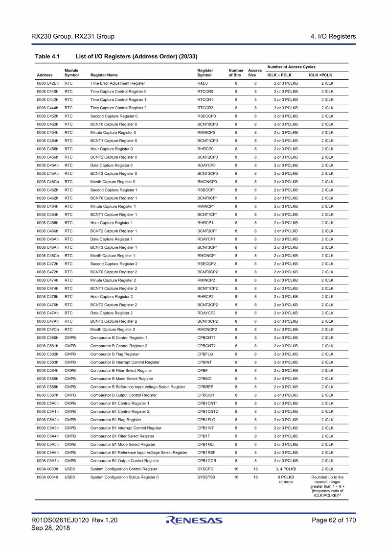
R01DS0261EJ0120 Rev.1.20 Page 62 of 170Sep 28, 2018
RX230 Group, RX231 Group 4. I/O Registers
0008 C42Eh RTC Time Error Adjustment Register RADJ 8 8 2 or 3 PCLKB 2 ICLK
0008 C440h RTC Time Capture Control Register 0 RTCCR0 8 8 2 or 3 PCLKB 2 ICLK
0008 C442h RTC Time Capture Control Register 1 RTCCR1 8 8 2 or 3 PCLKB 2 ICLK
0008 C444h RTC Time Capture Control Register 2 RTCCR2 8 8 2 or 3 PCLKB 2 ICLK
0008 C452h RTC Second Capture Register 0 RSECCP0 8 8 2 or 3 PCLKB 2 ICLK
0008 C452h RTC BCNT0 Capture Register 0 BCNT0CP0 8 8 2 or 3 PCLKB 2 ICLK
0008 C454h RTC Minute Capture Register 0 RMINCP0 8 8 2 or 3 PCLKB 2 ICLK
0008 C454h RTC BCNT1 Capture Register 0 BCNT1CP0 8 8 2 or 3 PCLKB 2 ICLK
0008 C456h RTC Hour Capture Register 0 RHRCP0 8 8 2 or 3 PCLKB 2 ICLK
0008 C456h RTC BCNT2 Capture Register 0 BCNT2CP0 8 8 2 or 3 PCLKB 2 ICLK
0008 C45Ah RTC Date Capture Register 0 RDAYCP0 8 8 2 or 3 PCLKB 2 ICLK
0008 C45Ah RTC BCNT3 Capture Register 0 BCNT3CP0 8 8 2 or 3 PCLKB 2 ICLK
0008 C45Ch RTC Month Capture Register 0 RMONCP0 8 8 2 or 3 PCLKB 2 ICLK
0008 C462h RTC Second Capture Register 1 RSECCP1 8 8 2 or 3 PCLKB 2 ICLK
0008 C462h RTC BCNT0 Capture Register 1 BCNT0CP1 8 8 2 or 3 PCLKB 2 ICLK
0008 C464h RTC Minute Capture Register 1 RMINCP1 8 8 2 or 3 PCLKB 2 ICLK
0008 C464h RTC BCNT1 Capture Register 1 BCNT1CP1 8 8 2 or 3 PCLKB 2 ICLK
0008 C466h RTC Hour Capture Register 1 RHRCP1 8 8 2 or 3 PCLKB 2 ICLK
0008 C466h RTC BCNT2 Capture Register 1 BCNT2CP1 8 8 2 or 3 PCLKB 2 ICLK
0008 C46Ah RTC Date Capture Register 1 RDAYCP1 8 8 2 or 3 PCLKB 2 ICLK
0008 C46Ah RTC BCNT3 Capture Register 1 BCNT3CP1 8 8 2 or 3 PCLKB 2 ICLK
0008 C46Ch RTC Month Capture Register 1 RMONCP1 8 8 2 or 3 PCLKB 2 ICLK
0008 C472h RTC Second Capture Register 2 RSECCP2 8 8 2 or 3 PCLKB 2 ICLK
0008 C472h RTC BCNT0 Capture Register 2 BCNT0CP2 8 8 2 or 3 PCLKB 2 ICLK
0008 C474h RTC Minute Capture Register 2 RMINCP2 8 8 2 or 3 PCLKB 2 ICLK
0008 C474h RTC BCNT1 Capture Register 2 BCNT1CP2 8 8 2 or 3 PCLKB 2 ICLK
0008 C476h RTC Hour Capture Register 2 RHRCP2 8 8 2 or 3 PCLKB 2 ICLK
0008 C476h RTC BCNT2 Capture Register 2 BCNT2CP2 8 8 2 or 3 PCLKB 2 ICLK
0008 C47Ah RTC Date Capture Register 2 RDAYCP2 8 8 2 or 3 PCLKB 2 ICLK
0008 C47Ah RTC BCNT3 Capture Register 2 BCNT3CP2 8 8 2 or 3 PCLKB 2 ICLK
0008 C47Ch RTC Month Capture Register 2 RMONCP2 8 8 2 or 3 PCLKB 2 ICLK
0008 C580h CMPB Comparator B Control Register 1 CPBCNT1 8 8 2 or 3 PCLKB 2 ICLK
0008 C581h CMPB Comparator B Control Register 2 CPBCNT2 8 8 2 or 3 PCLKB 2 ICLK
0008 C582h CMPB Comparator B Flag Register CPBFLG 8 8 2 or 3 PCLKB 2 ICLK
0008 C583h CMPB Comparator B Interrupt Control Register CPBINT 8 8 2 or 3 PCLKB 2 ICLK
0008 C584h CMPB Comparator B Filter Select Register CPBF 8 8 2 or 3 PCLKB 2 ICLK
0008 C585h CMPB Comparator B Mode Select Register CPBMD 8 8 2 or 3 PCLKB 2 ICLK
0008 C586h CMPB Comparator B Reference Input Voltage Select Register CPBREF 8 8 2 or 3 PCLKB 2 ICLK
0008 C587h CMPB Comparator B Output Control Register CPBOCR 8 8 2 or 3 PCLKB 2 ICLK
0008 C5A0h CMPB Comparator B1 Control Register 1 CPB1CNT1 8 8 2 or 3 PCLKB 2 ICLK
0008 C5A1h CMPB Comparator B1 Control Register 2 CPB1CNT2 8 8 2 or 3 PCLKB 2 ICLK
0008 C5A2h CMPB Comparator B1 Flag Register CPB1FLG 8 8 2 or 3 PCLKB 2 ICLK
0008 C5A3h CMPB Comparator B1 Interrupt Control Register CPB1INT 8 8 2 or 3 PCLKB 2 ICLK
0008 C5A4h CMPB Comparator B1 Filter Select Register CPB1F 8 8 2 or 3 PCLKB 2 ICLK
0008 C5A5h CMPB Comparator B1 Mode Select Register CPB1MD 8 8 2 or 3 PCLKB 2 ICLK
0008 C5A6h CMPB Comparator B1 Reference Input Voltage Select Register CPB1REF 8 8 2 or 3 PCLKB 2 ICLK
0008 C5A7h CMPB Comparator B1 Output Control Register CPB1OCR 8 8 2 or 3 PCLKB 2 ICLK
000A 0000h USB0 System Configuration Control Register SYSCFG 16 16 3, 4 PCLKB 2 ICLK
000A 0004h USB0 System Configuration Status Register 0 SYSSTS0 16 16 9 PCLKBor more
Rounded up to the nearest integer
greater than 1 + 9 × (frequency ratio of
ICLK/PCLKB)*2
Table 4.1 List of I/O Registers (Address Order) (20/33)
AddressModule Symbol Register Name
Register Symbol
Number of Bits
Access Size
Number of Access Cycles
ICLK ≥ PCLK ICLK <PCLK

R01DS0261EJ0120 Rev.1.20 Page 63 of 170Sep 28, 2018
RX230 Group, RX231 Group 4. I/O Registers
000A 0008h USB0 Device State Control Register 0 DVSTCTR0 16 16 9 PCLKBor more
Rounded up to the nearest integer
greater than 1 + 9 × (frequency ratio of
ICLK/PCLKB)*2
000A 0014h USB0 CFIFO Port Register CFIFO 16 16 3, 4 PCLKB 2 ICLK
000A 0018h USB0 D0FIFO Port Register D0FIFO 16 16 3, 4 PCLKB 2 ICLK
000A 001Ch USB0 D1FIFO Port Register D1FIFO 16 16 3, 4 PCLKB 2 ICLK
000A 0020h USB0 CFIFO Port Select Register CFIFOSEL 16 16 3, 4 PCLKB 2 ICLK
000A 0022h USB0 CFIFO Port Control Register CFIFOCTR 16 16 3, 4 PCLKB 2 ICLK
000A 0028h USB0 D0FIFO Port Select Register D0FIFOSEL 16 16 3, 4 PCLKB 2 ICLK
000A 002Ah USB0 D0FIFO Port Control Register D0FIFOCTR 16 16 3, 4 PCLKB 2 ICLK
000A 002Ch USB0 D1FIFO Port Select Register D1FIFOSEL 16 16 3, 4 PCLKB 2 ICLK
000A 002Eh USB0 D1FIFO Port Control Register D1FIFOCTR 16 16 3, 4 PCLKB 2 ICLK
000A 0030h USB0 Interrupt Enable Register 0 INTENB0 16 16 9 PCLKBor more
Frequency with 1 + 9 × (frequency ratio of
ICLK/PCLKB)*2
000A 0032h USB0 Interrupt Enable Register 1 INTENB1 16 16 9 PCLKBor more
Frequency with 1 + 9 × (frequency ratio of
ICLK/PCLKB)*2
000A 0036h USB0 BRDY Interrupt Enable Register BRDYENB 16 16 9 PCLKBor more
Frequency with 1 + 9 × (frequency ratio of
ICLK/PCLKB)*2
000A 0038h USB0 NRDY Interrupt Enable Register NRDYENB 16 16 9 PCLKBor more
Frequency with 1 + 9 × (frequency ratio of
ICLK/PCLKB)*2
000A 003Ah USB0 BEMP Interrupt Enable Register BEMPENB 16 16 9 PCLKBor more
Frequency with 1 + 9 × (frequency ratio of
ICLK/PCLKB)*2
000A 003Ch USB0 SOF Output Configuration Register SOFCFG 16 16 9 PCLKBor more
Frequency with 1 + 9 × (frequency ratio of
ICLK/PCLKB)*2
000A 0040h USB0 Interrupt Status Register 0 INTSTS0 16 16 9 PCLKBor more
Frequency with 1 + 9 × (frequency ratio of
ICLK/PCLKB)*2
000A 0042h USB0 Interrupt Status Register 1 INTSTS1 16 16 9 PCLKBor more
Frequency with 1 + 9 × (frequency ratio of
ICLK/PCLKB)*2
000A 0046h USB0 BRDY Interrupt Status Register BRDYSTS 16 16 9 PCLKBor more
Frequency with 1 + 9 × (frequency ratio of
ICLK/PCLKB)*2
000A 0048h USB0 NRDY Interrupt Status Register NRDYSTS 16 16 9 PCLKBor more
Frequency with 1 + 9 × (frequency ratio of
ICLK/PCLKB)*2
000A 004Ah USB0 BEMP Interrupt Status Register BEMPSTS 16 16 9 PCLKBor more
Frequency with 1 + 9 × (frequency ratio of
ICLK/PCLKB)*2
000A 004Ch USB0 Frame Number Register FRMNUM 16 16 9 PCLKBor more
Frequency with 1 + 9 × (frequency ratio of
ICLK/PCLKB)*2
000A 0054h USB0 USB Request Type Register USBREQ 16 16 9 PCLKBor more
Frequency with 1 + 9 × (frequency ratio of
ICLK/PCLKB)*2
000A 0056h USB0 USB Request Value Register USBVAL 16 16 9 PCLKBor more
Frequency with 1 + 9 × (frequency ratio of
ICLK/PCLKB)*2
000A 0058h USB0 USB Request Index Register USBINDX 16 16 9 PCLKBor more
Frequency with 1 + 9 × (frequency ratio of
ICLK/PCLKB)*2
000A 005Ah USB0 USB Request Length Register USBLENG 16 16 9 PCLKBor more
Frequency with 1 + 9 × (frequency ratio of
ICLK/PCLKB)*2
000A 005Ch USB0 DCP Configuration Register DCPCFG 16 16 9 PCLKBor more
Frequency with 1 + 9 × (frequency ratio of
ICLK/PCLKB)*2
000A 005Eh USB0 DCP Maximum Packet Size Register DCPMAXP 16 16 9 PCLKBor more
Frequency with 1 + 9 × (frequency ratio of
ICLK/PCLKB)*2
Table 4.1 List of I/O Registers (Address Order) (21/33)
AddressModule Symbol Register Name
Register Symbol
Number of Bits
Access Size
Number of Access Cycles
ICLK ≥ PCLK ICLK <PCLK
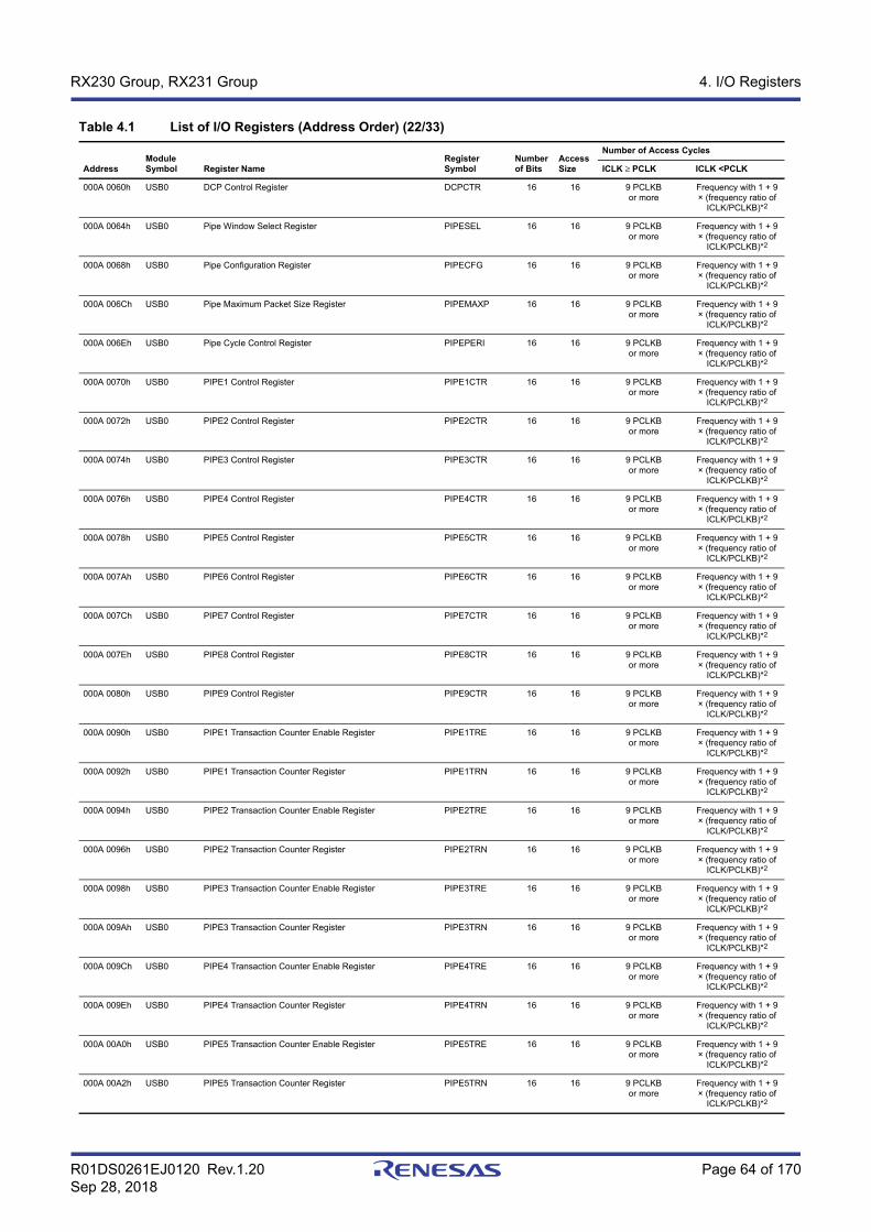
R01DS0261EJ0120 Rev.1.20 Page 64 of 170Sep 28, 2018
RX230 Group, RX231 Group 4. I/O Registers
000A 0060h USB0 DCP Control Register DCPCTR 16 16 9 PCLKBor more
Frequency with 1 + 9 × (frequency ratio of
ICLK/PCLKB)*2
000A 0064h USB0 Pipe Window Select Register PIPESEL 16 16 9 PCLKBor more
Frequency with 1 + 9 × (frequency ratio of
ICLK/PCLKB)*2
000A 0068h USB0 Pipe Configuration Register PIPECFG 16 16 9 PCLKBor more
Frequency with 1 + 9 × (frequency ratio of
ICLK/PCLKB)*2
000A 006Ch USB0 Pipe Maximum Packet Size Register PIPEMAXP 16 16 9 PCLKBor more
Frequency with 1 + 9 × (frequency ratio of
ICLK/PCLKB)*2
000A 006Eh USB0 Pipe Cycle Control Register PIPEPERI 16 16 9 PCLKBor more
Frequency with 1 + 9 × (frequency ratio of
ICLK/PCLKB)*2
000A 0070h USB0 PIPE1 Control Register PIPE1CTR 16 16 9 PCLKBor more
Frequency with 1 + 9 × (frequency ratio of
ICLK/PCLKB)*2
000A 0072h USB0 PIPE2 Control Register PIPE2CTR 16 16 9 PCLKBor more
Frequency with 1 + 9 × (frequency ratio of
ICLK/PCLKB)*2
000A 0074h USB0 PIPE3 Control Register PIPE3CTR 16 16 9 PCLKBor more
Frequency with 1 + 9 × (frequency ratio of
ICLK/PCLKB)*2
000A 0076h USB0 PIPE4 Control Register PIPE4CTR 16 16 9 PCLKBor more
Frequency with 1 + 9 × (frequency ratio of
ICLK/PCLKB)*2
000A 0078h USB0 PIPE5 Control Register PIPE5CTR 16 16 9 PCLKBor more
Frequency with 1 + 9 × (frequency ratio of
ICLK/PCLKB)*2
000A 007Ah USB0 PIPE6 Control Register PIPE6CTR 16 16 9 PCLKBor more
Frequency with 1 + 9 × (frequency ratio of
ICLK/PCLKB)*2
000A 007Ch USB0 PIPE7 Control Register PIPE7CTR 16 16 9 PCLKBor more
Frequency with 1 + 9 × (frequency ratio of
ICLK/PCLKB)*2
000A 007Eh USB0 PIPE8 Control Register PIPE8CTR 16 16 9 PCLKBor more
Frequency with 1 + 9 × (frequency ratio of
ICLK/PCLKB)*2
000A 0080h USB0 PIPE9 Control Register PIPE9CTR 16 16 9 PCLKBor more
Frequency with 1 + 9 × (frequency ratio of
ICLK/PCLKB)*2
000A 0090h USB0 PIPE1 Transaction Counter Enable Register PIPE1TRE 16 16 9 PCLKBor more
Frequency with 1 + 9 × (frequency ratio of
ICLK/PCLKB)*2
000A 0092h USB0 PIPE1 Transaction Counter Register PIPE1TRN 16 16 9 PCLKBor more
Frequency with 1 + 9 × (frequency ratio of
ICLK/PCLKB)*2
000A 0094h USB0 PIPE2 Transaction Counter Enable Register PIPE2TRE 16 16 9 PCLKBor more
Frequency with 1 + 9 × (frequency ratio of
ICLK/PCLKB)*2
000A 0096h USB0 PIPE2 Transaction Counter Register PIPE2TRN 16 16 9 PCLKBor more
Frequency with 1 + 9 × (frequency ratio of
ICLK/PCLKB)*2
000A 0098h USB0 PIPE3 Transaction Counter Enable Register PIPE3TRE 16 16 9 PCLKBor more
Frequency with 1 + 9 × (frequency ratio of
ICLK/PCLKB)*2
000A 009Ah USB0 PIPE3 Transaction Counter Register PIPE3TRN 16 16 9 PCLKBor more
Frequency with 1 + 9 × (frequency ratio of
ICLK/PCLKB)*2
000A 009Ch USB0 PIPE4 Transaction Counter Enable Register PIPE4TRE 16 16 9 PCLKBor more
Frequency with 1 + 9 × (frequency ratio of
ICLK/PCLKB)*2
000A 009Eh USB0 PIPE4 Transaction Counter Register PIPE4TRN 16 16 9 PCLKBor more
Frequency with 1 + 9 × (frequency ratio of
ICLK/PCLKB)*2
000A 00A0h USB0 PIPE5 Transaction Counter Enable Register PIPE5TRE 16 16 9 PCLKBor more
Frequency with 1 + 9 × (frequency ratio of
ICLK/PCLKB)*2
000A 00A2h USB0 PIPE5 Transaction Counter Register PIPE5TRN 16 16 9 PCLKBor more
Frequency with 1 + 9 × (frequency ratio of
ICLK/PCLKB)*2
Table 4.1 List of I/O Registers (Address Order) (22/33)
AddressModule Symbol Register Name
Register Symbol
Number of Bits
Access Size
Number of Access Cycles
ICLK ≥ PCLK ICLK <PCLK

R01DS0261EJ0120 Rev.1.20 Page 65 of 170Sep 28, 2018
RX230 Group, RX231 Group 4. I/O Registers
000A 00B0h USB0 BC Control Register 0 USBBCCTRL0 16 16 9 PCLKBor more
Frequency with 1 + 9 × (frequency ratio of
ICLK/PCLKB)*2
000A 00CCh USB0 USB Module Control Register USBMC 16 16 9 PCLKBor more
Frequency with 1 + 9 × (frequency ratio of
ICLK/PCLKB)*2
000A 00D0h USB0 Device Address 0 Configuration Register DEVADD0 16 16 9 PCLKBor more
Frequency with 1 + 9 × (frequency ratio of
ICLK/PCLKB)*2
000A 00D2h USB0 Device Address 1 Configuration Register DEVADD1 16 16 9 PCLKBor more
Frequency with 1 + 9 × (frequency ratio of
ICLK/PCLKB)*2
000A 00D4h USB0 Device Address 2 Configuration Register DEVADD2 16 16 9 PCLKBor more
Frequency with 1 + 9 × (frequency ratio of
ICLK/PCLKB)*2
000A 00D6h USB0 Device Address 3 Configuration Register DEVADD3 16 16 9 PCLKBor more
Frequency with 1 + 9 × (frequency ratio of
ICLK/PCLKB)*2
000A 00D8h USB0 Device Address 4 Configuration Register DEVADD4 16 16 9 PCLKBor more
Frequency with 1 + 9 × (frequency ratio of
ICLK/PCLKB)*2
000A 00DAh USB0 Device Address 5 Configuration Register DEVADD5 16 16 9 PCLKBor more
Frequency with 1 + 9 × (frequency ratio of
ICLK/PCLKB)*2
000A 0900h CTSU CTSU Control Register 0 CTSUCR0 8 8 2 or 3 PCLKB 2 ICLK
000A 0901h CTSU CTSU Control Register 1 CTSUCR1 8 8 2 or 3 PCLKB 2 ICLK
000A 0902h CTSU CTSU Synchronous Noise Reduction Setting Register CTSUSDPRS 8 8 2 or 3 PCLKB 2 ICLK
000A 0903h CTSU CTSU Sensor Stabilization Wait Control Register CTSUSST 8 8 2 or 3 PCLKB 2 ICLK
000A 0904h CTSU CTSU Measurement Channel Register 0 CTSUMCH0 8 8 2 or 3 PCLKB 2 ICLK
000A 0905h CTSU CTSU Measurement Channel Register 1 CTSUMCH1 8 8 2 or 3 PCLKB 2 ICLK
000A 0906h CTSU CTSU Channel Enable Control Register 0 CTSUCHAC0 8 8 2 or 3 PCLKB 2 ICLK
000A 0907h CTSU CTSU Channel Enable Control Register 1 CTSUCHAC1 8 8 2 or 3 PCLKB 2 ICLK
000A 0908h CTSU CTSU Channel Enable Control Register 2 CTSUCHAC2 8 8 2 or 3 PCLKB 2 ICLK
000A 0909h CTSU CTSU Channel Enable Control Register 3 CTSUCHAC3 8 8 2 or 3 PCLKB 2 ICLK
000A 090Ah CTSU CTSU Channel Enable Control Register 4 CTSUCHAC4 8 8 2 or 3 PCLKB 2 ICLK
000A 090Bh CTSU CTSU Channel Transmit/Receive Control Register 0 CTSUCHTRC0 8 8 2 or 3 PCLKB 2 ICLK
000A 090Ch CTSU CTSU Channel Transmit/Receive Control Register 1 CTSUCHTRC1 8 8 2 or 3 PCLKB 2 ICLK
000A 090Dh CTSU CTSU Channel Transmit/Receive Control Register 2 CTSUCHTRC2 8 8 2 or 3 PCLKB 2 ICLK
000A 090Eh CTSU CTSU Channel Transmit/Receive Control Register 3 CTSUCHTRC3 8 8 2 or 3 PCLKB 2 ICLK
000A 090Fh CTSU CTSU Channel Transmit/Receive Control Register 4 CTSUCHTRC4 8 8 2 or 3 PCLKB 2 ICLK
000A 0910h CTSU CTSU High-Pass Noise Reduction Control Register CTSUDCLKC 8 8 2 or 3 PCLKB 2 ICLK
000A 0911h CTSU CTSU Status Register CTSUST 8 8 2 or 3 PCLKB 2 ICLK
000A 0912h CTSU CTSU High-Pass Noise Reduction Spectrum Diffusion Control Register
CTSUSSC 16 16 2 or 3 PCLKB 2 ICLK
000A 0914h CTSU CTSU Sensor Offset Register 0 CTSUSO0 16 16 2 or 3 PCLKB 2 ICLK
000A 0916h CTSU CTSU Sensor Offset Register 1 CTSUSO1 16 16 2 or 3 PCLKB 2 ICLK
000A 0918h CTSU CTSU Sensor Counter CTSUSC 16 16 2 or 3 PCLKB 2 ICLK
000A 091Ah CTSU CTSU Reference Counter CTSURC 16 16 2 or 3 PCLKB 2 ICLK
000A 091Ch CTSU CTSU Error Status Register CTSUERRS 16 16 2 or 3 PCLKB 2 ICLK
000A 8300h RSCAN0 Bit Configuration Register L CFGL 16 16 2 or 3 PCLKB 2 ICLK
000A 8302h RSCAN0 Bit Configuration Register H CFGH 16 16 2 or 3 PCLKB 2 ICLK
000A 8304h RSCAN0 Control Register L CTRL 16 16 2 or 3 PCLKB 2 ICLK
000A 8306h RSCAN0 Control Register H CTRH 16 16 2 or 3 PCLKB 2 ICLK
000A 8308h RSCAN0 Status Register L STSL 16 16 2 or 3 PCLKB 2 ICLK
000A 830Ah RSCAN0 Status Register H STSH 16 16 2 or 3 PCLKB 2 ICLK
000A 830Ch RSCAN0 Error Flag Register L ERFLL 16 16 2 or 3 PCLKB 2 ICLK
000A 830Eh RSCAN0 Error Flag Register H ERFLH 16 16 2 or 3 PCLKB 2 ICLK
000A 8322h RSCAN Global Configuration Register L GCFGL 16 16 2 or 3 PCLKB 2 ICLK
000A 8324h RSCAN Global Configuration Register H GCFGH 16 16 2 or 3 PCLKB 2 ICLK
Table 4.1 List of I/O Registers (Address Order) (23/33)
AddressModule Symbol Register Name
Register Symbol
Number of Bits
Access Size
Number of Access Cycles
ICLK ≥ PCLK ICLK <PCLK
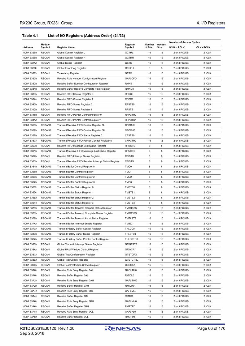
R01DS0261EJ0120 Rev.1.20 Page 66 of 170Sep 28, 2018
RX230 Group, RX231 Group 4. I/O Registers
000A 8326h RSCAN Global Control Register L GCTRL 16 16 2 or 3 PCLKB 2 ICLK
000A 8328h RSCAN Global Control Register H GCTRH 16 16 2 or 3 PCLKB 2 ICLK
000A 832Ah RSCAN Global Status Register GSTS 16 16 2 or 3 PCLKB 2 ICLK
000A 832Ch RSCAN Global Error Flag Register GERFLL 8 8 2 or 3 PCLKB 2 ICLK
000A 832Eh RSCAN Timestamp Register GTSC 16 16 2 or 3 PCLKB 2 ICLK
000A 8330h RSCAN Receive Rule Number Configuration Register GAFLCFG 16 16 2 or 3 PCLKB 2 ICLK
000A 8332h RSCAN Receive Buffer Number Configuration Register RMNB 16 16 2 or 3 PCLKB 2 ICLK
000A 8334h RSCAN Receive Buffer Receive Complete Flag Register RMND0 16 16 2 or 3 PCLKB 2 ICLK
000A 8338h RSCAN Receive FIFO Control Register 0 RFCC0 16 16 2 or 3 PCLKB 2 ICLK
000A 833Ah RSCAN Receive FIFO Control Register 1 RFCC1 16 16 2 or 3 PCLKB 2 ICLK
000A 8340h RSCAN Receive FIFO Status Register 0 RFSTS0 16 16 2 or 3 PCLKB 2 ICLK
000A 8342h RSCAN Receive FIFO Status Register 1 RFSTS1 16 16 2 or 3 PCLKB 2 ICLK
000A 8348h RSCAN Receive FIFO Pointer Control Register 0 RFPCTR0 16 16 2 or 3 PCLKB 2 ICLK
000A 834Ah RSCAN Receive FIFO Pointer Control Register 1 RFPCTR1 16 16 2 or 3 PCLKB 2 ICLK
000A 8350h RSCAN0 Transmit/Receive FIFO Control Register 0L CFCCL0 16 16 2 or 3 PCLKB 2 ICLK
000A 8352h RSCAN0 Transmit/Receive FIFO Control Register 0H CFCCH0 16 16 2 or 3 PCLKB 2 ICLK
000A 8358h RSCAN0 Transmit/Receive FIFO Status Register 0 CFSTS0 16 16 2 or 3 PCLKB 2 ICLK
000A 835Ch RSCAN0 Transmit/Receive FIFO Pointer Control Register 0 CFPCTR0 16 16 2 or 3 PCLKB 2 ICLK
000A 8360h RSCAN Receive FIFO Message Lost Status Register RFMSTS 8 8 2 or 3 PCLKB 2 ICLK
000A 8361h RSCAN0 Transmit/Receive FIFO Message Lost Status Register CFMSTS 8 8 2 or 3 PCLKB 2 ICLK
000A 8362h RSCAN Receive FIFO Interrupt Status Register RFISTS 8 8 2 or 3 PCLKB 2 ICLK
000A 8363h RSCAN Transmit/Receive FIFO Receive Interrupt Status Register CFISTS 8 8 2 or 3 PCLKB 2 ICLK
000A 8364h RSCAN0 Transmit Buffer Control Register 0 TMC0 8 8 2 or 3 PCLKB 2 ICLK
000A 8365h RSCAN0 Transmit Buffer Control Register 1 TMC1 8 8 2 or 3 PCLKB 2 ICLK
000A 8366h RSCAN0 Transmit Buffer Control Register 2 TMC2 8 8 2 or 3 PCLKB 2 ICLK
000A 8367h RSCAN0 Transmit Buffer Control Register 3 TMC3 8 8 2 or 3 PCLKB 2 ICLK
000A 836Ch RSCAN0 Transmit Buffer Status Register 0 TMSTS0 8 8 2 or 3 PCLKB 2 ICLK
000A 836Dh RSCAN0 Transmit Buffer Status Register 1 TMSTS1 8 8 2 or 3 PCLKB 2 ICLK
000A 836Eh RSCAN0 Transmit Buffer Status Register 2 TMSTS2 8 8 2 or 3 PCLKB 2 ICLK
000A 836Fh RSCAN0 Transmit Buffer Status Register 3 TMSTS3 8 8 2 or 3 PCLKB 2 ICLK
000A 8374h RSCAN0 Transmit Buffer Transmit Request Status Register TMTRSTS 16 16 2 or 3 PCLKB 2 ICLK
000A 8376h RSCAN0 Transmit Buffer Transmit Complete Status Register TMTCSTS 16 16 2 or 3 PCLKB 2 ICLK
000A 8378h RSCAN0 Transmit Buffer Transmit Abort Status Register TMTASTS 16 16 2 or 3 PCLKB 2 ICLK
000A 837Ah RSCAN0 Transmit Buffer Interrupt Enable Register TMIEC 16 16 2 or 3 PCLKB 2 ICLK
000A 837Ch RSCAN0 Transmit History Buffer Control Register THLCC0 16 16 2 or 3 PCLKB 2 ICLK
000A 8380h RSCAN0 Transmit History Buffer Status Register THLSTS0 16 16 2 or 3 PCLKB 2 ICLK
000A 8384h RSCAN0 Transmit History Buffer Pointer Control Register THLPCTR0 16 16 2 or 3 PCLKB 2 ICLK
000A 8388h RSCAN Global Transmit Interrupt Status Register GTINTSTS 16 16 2 or 3 PCLKB 2 ICLK
000A 838Ah RSCAN Global RAM Window Control Register GRWCR 16 16 2 or 3 PCLKB 2 ICLK
000A 838Ch RSCAN Global Test Configuration Register GTSTCFG 16 16 2 or 3 PCLKB 2 ICLK
000A 838Eh RSCAN Global Test Control Register GTSTCTRL 16 16 2 or 3 PCLKB 2 ICLK
000A 8394h RSCAN Global Test Protection Unlock Register GLOCKK 16 16 2 or 3 PCLKB 2 ICLK
000A 83A0h RSCAN Receive Rule Entry Register 0AL GAFLIDL0 16 16 2 or 3 PCLKB 2 ICLK
000A 83A0h RSCAN Receive Buffer Register 0AL RMIDL0 16 16 2 or 3 PCLKB 2 ICLK
000A 83A2h RSCAN Receive Rule Entry Register 0AH GAFLIDH0 16 16 2 or 3 PCLKB 2 ICLK
000A 83A2h RSCAN Receive Buffer Register 0AH RMIDH0 16 16 2 or 3 PCLKB 2 ICLK
000A 83A4h RSCAN Receive Rule Entry Register 0BL GAFLML0 16 16 2 or 3 PCLKB 2 ICLK
000A 83A4h RSCAN Receive Buffer Register 0BL RMTS0 16 16 2 or 3 PCLKB 2 ICLK
000A 83A6h RSCAN Receive Rule Entry Register 0BH GAFLMH0 16 16 2 or 3 PCLKB 2 ICLK
000A 83A6h RSCAN Receive Buffer Register 0BH RMPTR0 16 16 2 or 3 PCLKB 2 ICLK
000A 83A8h RSCAN Receive Rule Entry Register 0CL GAFLPL0 16 16 2 or 3 PCLKB 2 ICLK
000A 83A8h RSCAN Receive Buffer Register 0CL RMDF00 16 16 2 or 3 PCLKB 2 ICLK
Table 4.1 List of I/O Registers (Address Order) (24/33)
AddressModule Symbol Register Name
Register Symbol
Number of Bits
Access Size
Number of Access Cycles
ICLK ≥ PCLK ICLK <PCLK
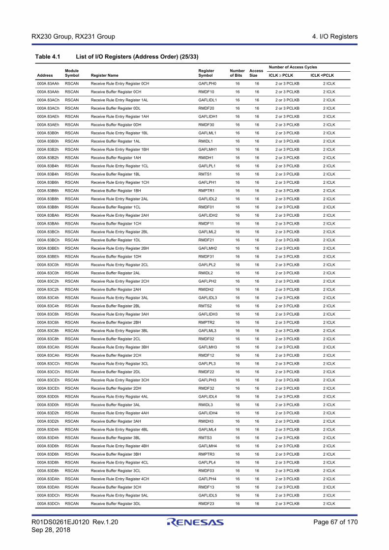
R01DS0261EJ0120 Rev.1.20 Page 67 of 170Sep 28, 2018
RX230 Group, RX231 Group 4. I/O Registers
000A 83AAh RSCAN Receive Rule Entry Register 0CH GAFLPH0 16 16 2 or 3 PCLKB 2 ICLK
000A 83AAh RSCAN Receive Buffer Register 0CH RMDF10 16 16 2 or 3 PCLKB 2 ICLK
000A 83ACh RSCAN Receive Rule Entry Register 1AL GAFLIDL1 16 16 2 or 3 PCLKB 2 ICLK
000A 83ACh RSCAN Receive Buffer Register 0DL RMDF20 16 16 2 or 3 PCLKB 2 ICLK
000A 83AEh RSCAN Receive Rule Entry Register 1AH GAFLIDH1 16 16 2 or 3 PCLKB 2 ICLK
000A 83AEh RSCAN Receive Buffer Register 0DH RMDF30 16 16 2 or 3 PCLKB 2 ICLK
000A 83B0h RSCAN Receive Rule Entry Register 1BL GAFLML1 16 16 2 or 3 PCLKB 2 ICLK
000A 83B0h RSCAN Receive Buffer Register 1AL RMIDL1 16 16 2 or 3 PCLKB 2 ICLK
000A 83B2h RSCAN Receive Rule Entry Register 1BH GAFLMH1 16 16 2 or 3 PCLKB 2 ICLK
000A 83B2h RSCAN Receive Buffer Register 1AH RMIDH1 16 16 2 or 3 PCLKB 2 ICLK
000A 83B4h RSCAN Receive Rule Entry Register 1CL GAFLPL1 16 16 2 or 3 PCLKB 2 ICLK
000A 83B4h RSCAN Receive Buffer Register 1BL RMTS1 16 16 2 or 3 PCLKB 2 ICLK
000A 83B6h RSCAN Receive Rule Entry Register 1CH GAFLPH1 16 16 2 or 3 PCLKB 2 ICLK
000A 83B6h RSCAN Receive Buffer Register 1BH RMPTR1 16 16 2 or 3 PCLKB 2 ICLK
000A 83B8h RSCAN Receive Rule Entry Register 2AL GAFLIDL2 16 16 2 or 3 PCLKB 2 ICLK
000A 83B8h RSCAN Receive Buffer Register 1CL RMDF01 16 16 2 or 3 PCLKB 2 ICLK
000A 83BAh RSCAN Receive Rule Entry Register 2AH GAFLIDH2 16 16 2 or 3 PCLKB 2 ICLK
000A 83BAh RSCAN Receive Buffer Register 1CH RMDF11 16 16 2 or 3 PCLKB 2 ICLK
000A 83BCh RSCAN Receive Rule Entry Register 2BL GAFLML2 16 16 2 or 3 PCLKB 2 ICLK
000A 83BCh RSCAN Receive Buffer Register 1DL RMDF21 16 16 2 or 3 PCLKB 2 ICLK
000A 83BEh RSCAN Receive Rule Entry Register 2BH GAFLMH2 16 16 2 or 3 PCLKB 2 ICLK
000A 83BEh RSCAN Receive Buffer Register 1DH RMDF31 16 16 2 or 3 PCLKB 2 ICLK
000A 83C0h RSCAN Receive Rule Entry Register 2CL GAFLPL2 16 16 2 or 3 PCLKB 2 ICLK
000A 83C0h RSCAN Receive Buffer Register 2AL RMIDL2 16 16 2 or 3 PCLKB 2 ICLK
000A 83C2h RSCAN Receive Rule Entry Register 2CH GAFLPH2 16 16 2 or 3 PCLKB 2 ICLK
000A 83C2h RSCAN Receive Buffer Register 2AH RMIDH2 16 16 2 or 3 PCLKB 2 ICLK
000A 83C4h RSCAN Receive Rule Entry Register 3AL GAFLIDL3 16 16 2 or 3 PCLKB 2 ICLK
000A 83C4h RSCAN Receive Buffer Register 2BL RMTS2 16 16 2 or 3 PCLKB 2 ICLK
000A 83C6h RSCAN Receive Rule Entry Register 3AH GAFLIDH3 16 16 2 or 3 PCLKB 2 ICLK
000A 83C6h RSCAN Receive Buffer Register 2BH RMPTR2 16 16 2 or 3 PCLKB 2 ICLK
000A 83C8h RSCAN Receive Rule Entry Register 3BL GAFLML3 16 16 2 or 3 PCLKB 2 ICLK
000A 83C8h RSCAN Receive Buffer Register 2CL RMDF02 16 16 2 or 3 PCLKB 2 ICLK
000A 83CAh RSCAN Receive Rule Entry Register 3BH GAFLMH3 16 16 2 or 3 PCLKB 2 ICLK
000A 83CAh RSCAN Receive Buffer Register 2CH RMDF12 16 16 2 or 3 PCLKB 2 ICLK
000A 83CCh RSCAN Receive Rule Entry Register 3CL GAFLPL3 16 16 2 or 3 PCLKB 2 ICLK
000A 83CCh RSCAN Receive Buffer Register 2DL RMDF22 16 16 2 or 3 PCLKB 2 ICLK
000A 83CEh RSCAN Receive Rule Entry Register 3CH GAFLPH3 16 16 2 or 3 PCLKB 2 ICLK
000A 83CEh RSCAN Receive Buffer Register 2DH RMDF32 16 16 2 or 3 PCLKB 2 ICLK
000A 83D0h RSCAN Receive Rule Entry Register 4AL GAFLIDL4 16 16 2 or 3 PCLKB 2 ICLK
000A 83D0h RSCAN Receive Buffer Register 3AL RMIDL3 16 16 2 or 3 PCLKB 2 ICLK
000A 83D2h RSCAN Receive Rule Entry Register 4AH GAFLIDH4 16 16 2 or 3 PCLKB 2 ICLK
000A 83D2h RSCAN Receive Buffer Register 3AH RMIDH3 16 16 2 or 3 PCLKB 2 ICLK
000A 83D4h RSCAN Receive Rule Entry Register 4BL GAFLML4 16 16 2 or 3 PCLKB 2 ICLK
000A 83D4h RSCAN Receive Buffer Register 3BL RMTS3 16 16 2 or 3 PCLKB 2 ICLK
000A 83D6h RSCAN Receive Rule Entry Register 4BH GAFLMH4 16 16 2 or 3 PCLKB 2 ICLK
000A 83D6h RSCAN Receive Buffer Register 3BH RMPTR3 16 16 2 or 3 PCLKB 2 ICLK
000A 83D8h RSCAN Receive Rule Entry Register 4CL GAFLPL4 16 16 2 or 3 PCLKB 2 ICLK
000A 83D8h RSCAN Receive Buffer Register 3CL RMDF03 16 16 2 or 3 PCLKB 2 ICLK
000A 83DAh RSCAN Receive Rule Entry Register 4CH GAFLPH4 16 16 2 or 3 PCLKB 2 ICLK
000A 83DAh RSCAN Receive Buffer Register 3CH RMDF13 16 16 2 or 3 PCLKB 2 ICLK
000A 83DCh RSCAN Receive Rule Entry Register 5AL GAFLIDL5 16 16 2 or 3 PCLKB 2 ICLK
000A 83DCh RSCAN Receive Buffer Register 3DL RMDF23 16 16 2 or 3 PCLKB 2 ICLK
Table 4.1 List of I/O Registers (Address Order) (25/33)
AddressModule Symbol Register Name
Register Symbol
Number of Bits
Access Size
Number of Access Cycles
ICLK ≥ PCLK ICLK <PCLK
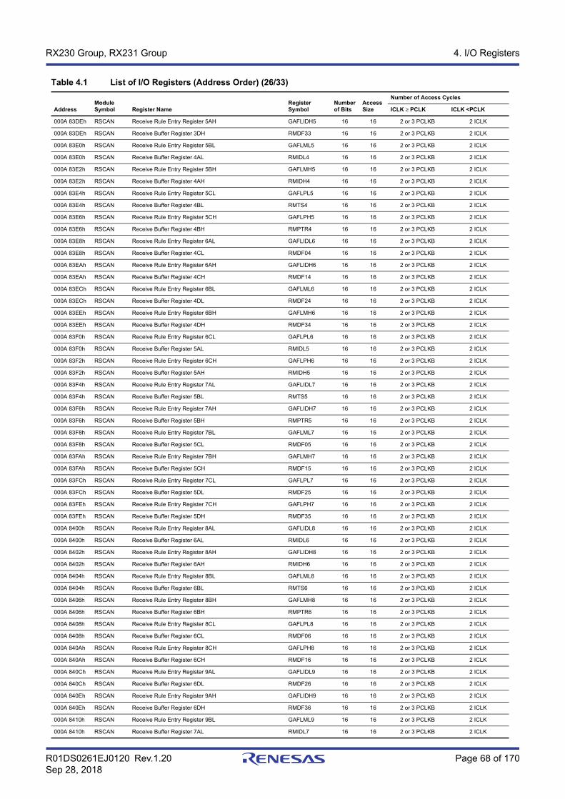
R01DS0261EJ0120 Rev.1.20 Page 68 of 170Sep 28, 2018
RX230 Group, RX231 Group 4. I/O Registers
000A 83DEh RSCAN Receive Rule Entry Register 5AH GAFLIDH5 16 16 2 or 3 PCLKB 2 ICLK
000A 83DEh RSCAN Receive Buffer Register 3DH RMDF33 16 16 2 or 3 PCLKB 2 ICLK
000A 83E0h RSCAN Receive Rule Entry Register 5BL GAFLML5 16 16 2 or 3 PCLKB 2 ICLK
000A 83E0h RSCAN Receive Buffer Register 4AL RMIDL4 16 16 2 or 3 PCLKB 2 ICLK
000A 83E2h RSCAN Receive Rule Entry Register 5BH GAFLMH5 16 16 2 or 3 PCLKB 2 ICLK
000A 83E2h RSCAN Receive Buffer Register 4AH RMIDH4 16 16 2 or 3 PCLKB 2 ICLK
000A 83E4h RSCAN Receive Rule Entry Register 5CL GAFLPL5 16 16 2 or 3 PCLKB 2 ICLK
000A 83E4h RSCAN Receive Buffer Register 4BL RMTS4 16 16 2 or 3 PCLKB 2 ICLK
000A 83E6h RSCAN Receive Rule Entry Register 5CH GAFLPH5 16 16 2 or 3 PCLKB 2 ICLK
000A 83E6h RSCAN Receive Buffer Register 4BH RMPTR4 16 16 2 or 3 PCLKB 2 ICLK
000A 83E8h RSCAN Receive Rule Entry Register 6AL GAFLIDL6 16 16 2 or 3 PCLKB 2 ICLK
000A 83E8h RSCAN Receive Buffer Register 4CL RMDF04 16 16 2 or 3 PCLKB 2 ICLK
000A 83EAh RSCAN Receive Rule Entry Register 6AH GAFLIDH6 16 16 2 or 3 PCLKB 2 ICLK
000A 83EAh RSCAN Receive Buffer Register 4CH RMDF14 16 16 2 or 3 PCLKB 2 ICLK
000A 83ECh RSCAN Receive Rule Entry Register 6BL GAFLML6 16 16 2 or 3 PCLKB 2 ICLK
000A 83ECh RSCAN Receive Buffer Register 4DL RMDF24 16 16 2 or 3 PCLKB 2 ICLK
000A 83EEh RSCAN Receive Rule Entry Register 6BH GAFLMH6 16 16 2 or 3 PCLKB 2 ICLK
000A 83EEh RSCAN Receive Buffer Register 4DH RMDF34 16 16 2 or 3 PCLKB 2 ICLK
000A 83F0h RSCAN Receive Rule Entry Register 6CL GAFLPL6 16 16 2 or 3 PCLKB 2 ICLK
000A 83F0h RSCAN Receive Buffer Register 5AL RMIDL5 16 16 2 or 3 PCLKB 2 ICLK
000A 83F2h RSCAN Receive Rule Entry Register 6CH GAFLPH6 16 16 2 or 3 PCLKB 2 ICLK
000A 83F2h RSCAN Receive Buffer Register 5AH RMIDH5 16 16 2 or 3 PCLKB 2 ICLK
000A 83F4h RSCAN Receive Rule Entry Register 7AL GAFLIDL7 16 16 2 or 3 PCLKB 2 ICLK
000A 83F4h RSCAN Receive Buffer Register 5BL RMTS5 16 16 2 or 3 PCLKB 2 ICLK
000A 83F6h RSCAN Receive Rule Entry Register 7AH GAFLIDH7 16 16 2 or 3 PCLKB 2 ICLK
000A 83F6h RSCAN Receive Buffer Register 5BH RMPTR5 16 16 2 or 3 PCLKB 2 ICLK
000A 83F8h RSCAN Receive Rule Entry Register 7BL GAFLML7 16 16 2 or 3 PCLKB 2 ICLK
000A 83F8h RSCAN Receive Buffer Register 5CL RMDF05 16 16 2 or 3 PCLKB 2 ICLK
000A 83FAh RSCAN Receive Rule Entry Register 7BH GAFLMH7 16 16 2 or 3 PCLKB 2 ICLK
000A 83FAh RSCAN Receive Buffer Register 5CH RMDF15 16 16 2 or 3 PCLKB 2 ICLK
000A 83FCh RSCAN Receive Rule Entry Register 7CL GAFLPL7 16 16 2 or 3 PCLKB 2 ICLK
000A 83FCh RSCAN Receive Buffer Register 5DL RMDF25 16 16 2 or 3 PCLKB 2 ICLK
000A 83FEh RSCAN Receive Rule Entry Register 7CH GAFLPH7 16 16 2 or 3 PCLKB 2 ICLK
000A 83FEh RSCAN Receive Buffer Register 5DH RMDF35 16 16 2 or 3 PCLKB 2 ICLK
000A 8400h RSCAN Receive Rule Entry Register 8AL GAFLIDL8 16 16 2 or 3 PCLKB 2 ICLK
000A 8400h RSCAN Receive Buffer Register 6AL RMIDL6 16 16 2 or 3 PCLKB 2 ICLK
000A 8402h RSCAN Receive Rule Entry Register 8AH GAFLIDH8 16 16 2 or 3 PCLKB 2 ICLK
000A 8402h RSCAN Receive Buffer Register 6AH RMIDH6 16 16 2 or 3 PCLKB 2 ICLK
000A 8404h RSCAN Receive Rule Entry Register 8BL GAFLML8 16 16 2 or 3 PCLKB 2 ICLK
000A 8404h RSCAN Receive Buffer Register 6BL RMTS6 16 16 2 or 3 PCLKB 2 ICLK
000A 8406h RSCAN Receive Rule Entry Register 8BH GAFLMH8 16 16 2 or 3 PCLKB 2 ICLK
000A 8406h RSCAN Receive Buffer Register 6BH RMPTR6 16 16 2 or 3 PCLKB 2 ICLK
000A 8408h RSCAN Receive Rule Entry Register 8CL GAFLPL8 16 16 2 or 3 PCLKB 2 ICLK
000A 8408h RSCAN Receive Buffer Register 6CL RMDF06 16 16 2 or 3 PCLKB 2 ICLK
000A 840Ah RSCAN Receive Rule Entry Register 8CH GAFLPH8 16 16 2 or 3 PCLKB 2 ICLK
000A 840Ah RSCAN Receive Buffer Register 6CH RMDF16 16 16 2 or 3 PCLKB 2 ICLK
000A 840Ch RSCAN Receive Rule Entry Register 9AL GAFLIDL9 16 16 2 or 3 PCLKB 2 ICLK
000A 840Ch RSCAN Receive Buffer Register 6DL RMDF26 16 16 2 or 3 PCLKB 2 ICLK
000A 840Eh RSCAN Receive Rule Entry Register 9AH GAFLIDH9 16 16 2 or 3 PCLKB 2 ICLK
000A 840Eh RSCAN Receive Buffer Register 6DH RMDF36 16 16 2 or 3 PCLKB 2 ICLK
000A 8410h RSCAN Receive Rule Entry Register 9BL GAFLML9 16 16 2 or 3 PCLKB 2 ICLK
000A 8410h RSCAN Receive Buffer Register 7AL RMIDL7 16 16 2 or 3 PCLKB 2 ICLK
Table 4.1 List of I/O Registers (Address Order) (26/33)
AddressModule Symbol Register Name
Register Symbol
Number of Bits
Access Size
Number of Access Cycles
ICLK ≥ PCLK ICLK <PCLK
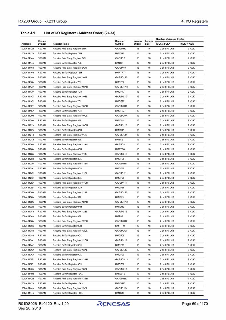
R01DS0261EJ0120 Rev.1.20 Page 69 of 170Sep 28, 2018
RX230 Group, RX231 Group 4. I/O Registers
000A 8412h RSCAN Receive Rule Entry Register 9BH GAFLMH9 16 16 2 or 3 PCLKB 2 ICLK
000A 8412h RSCAN Receive Buffer Register 7AH RMIDH7 16 16 2 or 3 PCLKB 2 ICLK
000A 8414h RSCAN Receive Rule Entry Register 9CL GAFLPL9 16 16 2 or 3 PCLKB 2 ICLK
000A 8414h RSCAN Receive Buffer Register 7BL RMTS7 16 16 2 or 3 PCLKB 2 ICLK
000A 8416h RSCAN Receive Rule Entry Register 9CH GAFLPH9 16 16 2 or 3 PCLKB 2 ICLK
000A 8416h RSCAN Receive Buffer Register 7BH RMPTR7 16 16 2 or 3 PCLKB 2 ICLK
000A 8418h RSCAN Receive Rule Entry Register 10AL GAFLIDL10 16 16 2 or 3 PCLKB 2 ICLK
000A 8418h RSCAN Receive Buffer Register 7CL RMDF07 16 16 2 or 3 PCLKB 2 ICLK
000A 841Ah RSCAN Receive Rule Entry Register 10AH GAFLIDH10 16 16 2 or 3 PCLKB 2 ICLK
000A 841Ah RSCAN Receive Buffer Register 7CH RMDF17 16 16 2 or 3 PCLKB 2 ICLK
000A 841Ch RSCAN Receive Rule Entry Register 10BL GAFLML10 16 16 2 or 3 PCLKB 2 ICLK
000A 841Ch RSCAN Receive Buffer Register 7DL RMDF27 16 16 2 or 3 PCLKB 2 ICLK
000A 841Eh RSCAN Receive Rule Entry Register 10BH GAFLMH10 16 16 2 or 3 PCLKB 2 ICLK
000A 841Eh RSCAN Receive Buffer Register 7DH RMDF37 16 16 2 or 3 PCLKB 2 ICLK
000A 8420h RSCAN Receive Rule Entry Register 10CL GAFLPL10 16 16 2 or 3 PCLKB 2 ICLK
000A 8420h RSCAN Receive Buffer Register 8AL RMIDL8 16 16 2 or 3 PCLKB 2 ICLK
000A 8422h RSCAN Receive Rule Entry Register 10CH GAFLPH10 16 16 2 or 3 PCLKB 2 ICLK
000A 8422h RSCAN Receive Buffer Register 8AH RMIDH8 16 16 2 or 3 PCLKB 2 ICLK
000A 8424h RSCAN Receive Rule Entry Register 11AL GAFLIDL11 16 16 2 or 3 PCLKB 2 ICLK
000A 8424h RSCAN Receive Buffer Register 8BL RMTS8 16 16 2 or 3 PCLKB 2 ICLK
000A 8426h RSCAN Receive Rule Entry Register 11AH GAFLIDH11 16 16 2 or 3 PCLKB 2 ICLK
000A 8426h RSCAN Receive Buffer Register 8BH RMPTR8 16 16 2 or 3 PCLKB 2 ICLK
000A 8428h RSCAN Receive Rule Entry Register 11BL GAFLML11 16 16 2 or 3 PCLKB 2 ICLK
000A 8428h RSCAN Receive Buffer Register 8CL RMDF08 16 16 2 or 3 PCLKB 2 ICLK
000A 842Ah RSCAN Receive Rule Entry Register 11BH GAFLMH11 16 16 2 or 3 PCLKB 2 ICLK
000A 842Ah RSCAN Receive Buffer Register 8CH RMDF18 16 16 2 or 3 PCLKB 2 ICLK
000A 842Ch RSCAN Receive Rule Entry Register 11CL GAFLPL11 16 16 2 or 3 PCLKB 2 ICLK
000A 842Ch RSCAN Receive Buffer Register 8DL RMDF28 16 16 2 or 3 PCLKB 2 ICLK
000A 842Eh RSCAN Receive Rule Entry Register 11CH GAFLPH11 16 16 2 or 3 PCLKB 2 ICLK
000A 842Eh RSCAN Receive Buffer Register 8DH RMDF38 16 16 2 or 3 PCLKB 2 ICLK
000A 8430h RSCAN Receive Rule Entry Register 12AL GAFLIDL12 16 16 2 or 3 PCLKB 2 ICLK
000A 8430h RSCAN Receive Buffer Register 9AL RMIDL9 16 16 2 or 3 PCLKB 2 ICLK
000A 8432h RSCAN Receive Rule Entry Register 12AH GAFLIDH12 16 16 2 or 3 PCLKB 2 ICLK
000A 8432h RSCAN Receive Buffer Register 9AH RMIDH9 16 16 2 or 3 PCLKB 2 ICLK
000A 8434h RSCAN Receive Rule Entry Register 12BL GAFLML12 16 16 2 or 3 PCLKB 2 ICLK
000A 8434h RSCAN Receive Buffer Register 9BL RMTS9 16 16 2 or 3 PCLKB 2 ICLK
000A 8436h RSCAN Receive Rule Entry Register 12BH GAFLMH12 16 16 2 or 3 PCLKB 2 ICLK
000A 8436h RSCAN Receive Buffer Register 9BH RMPTR9 16 16 2 or 3 PCLKB 2 ICLK
000A 8438h RSCAN Receive Rule Entry Register 12CL GAFLPL12 16 16 2 or 3 PCLKB 2 ICLK
000A 8438h RSCAN Receive Buffer Register 9CL RMDF09 16 16 2 or 3 PCLKB 2 ICLK
000A 843Ah RSCAN Receive Rule Entry Register 12CH GAFLPH12 16 16 2 or 3 PCLKB 2 ICLK
000A 843Ah RSCAN Receive Buffer Register 9CH RMDF19 16 16 2 or 3 PCLKB 2 ICLK
000A 843Ch RSCAN Receive Rule Entry Register 13AL GAFLIDL13 16 16 2 or 3 PCLKB 2 ICLK
000A 843Ch RSCAN Receive Buffer Register 9DL RMDF29 16 16 2 or 3 PCLKB 2 ICLK
000A 843Eh RSCAN Receive Rule Entry Register 13AH GAFLIDH13 16 16 2 or 3 PCLKB 2 ICLK
000A 843Eh RSCAN Receive Buffer Register 9DH RMDF39 16 16 2 or 3 PCLKB 2 ICLK
000A 8440h RSCAN Receive Rule Entry Register 13BL GAFLML13 16 16 2 or 3 PCLKB 2 ICLK
000A 8440h RSCAN Receive Buffer Register 10AL RMIDL10 16 16 2 or 3 PCLKB 2 ICLK
000A 8442h RSCAN Receive Rule Entry Register 13BH GAFLMH13 16 16 2 or 3 PCLKB 2 ICLK
000A 8442h RSCAN Receive Buffer Register 10AH RMIDH10 16 16 2 or 3 PCLKB 2 ICLK
000A 8444h RSCAN Receive Rule Entry Register 13CL GAFLPL13 16 16 2 or 3 PCLKB 2 ICLK
000A 8444h RSCAN Receive Buffer Register 10BL RMTS10 16 16 2 or 3 PCLKB 2 ICLK
Table 4.1 List of I/O Registers (Address Order) (27/33)
AddressModule Symbol Register Name
Register Symbol
Number of Bits
Access Size
Number of Access Cycles
ICLK ≥ PCLK ICLK <PCLK
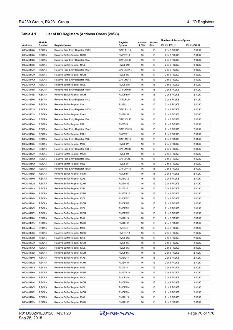
R01DS0261EJ0120 Rev.1.20 Page 70 of 170Sep 28, 2018
RX230 Group, RX231 Group 4. I/O Registers
000A 8446h RSCAN Receive Rule Entry Register 13CH GAFLPH13 16 16 2 or 3 PCLKB 2 ICLK
000A 8446h RSCAN Receive Buffer Register 10BH RMPTR10 16 16 2 or 3 PCLKB 2 ICLK
000A 8448h RSCAN Receive Rule Entry Register 14AL GAFLIDL14 16 16 2 or 3 PCLKB 2 ICLK
000A 8448h RSCAN Receive Buffer Register 10CL RMDF010 16 16 2 or 3 PCLKB 2 ICLK
000A 844Ah RSCAN Receive Rule Entry Register 14AH GAFLIDH14 16 16 2 or 3 PCLKB 2 ICLK
000A 844Ah RSCAN Receive Buffer Register 10CH RMDF110 16 16 2 or 3 PCLKB 2 ICLK
000A 844Ch RSCAN Receive Rule Entry Register 14BL GAFLML14 16 16 2 or 3 PCLKB 2 ICLK
000A 844Ch RSCAN Receive Buffer Register 10DL RMDF210 16 16 2 or 3 PCLKB 2 ICLK
000A 844Eh RSCAN Receive Rule Entry Register 14BH GAFLMH14 16 16 2 or 3 PCLKB 2 ICLK
000A 844Eh RSCAN Receive Buffer Register 10DH RMDF310 16 16 2 or 3 PCLKB 2 ICLK
000A 8450h RSCAN Receive Rule Entry Register 14CL GAFLPL14 16 16 2 or 3 PCLKB 2 ICLK
000A 8450h RSCAN Receive Buffer Register 11AL RMIDL11 16 16 2 or 3 PCLKB 2 ICLK
000A 8452h RSCAN Receive Rule Entry Register 14CH GAFLPH14 16 16 2 or 3 PCLKB 2 ICLK
000A 8452h RSCAN Receive Buffer Register 11AH RMIDH11 16 16 2 or 3 PCLKB 2 ICLK
000A 8454h RSCAN Receive Rule Entry Register 15AL GAFLIDL15 16 16 2 or 3 PCLKB 2 ICLK
000A 8454h RSCAN Receive Buffer Register 11BL RMTS11 16 16 2 or 3 PCLKB 2 ICLK
000A 8456h RSCAN Receive Rule Entry Register 15AH GAFLIDH15 16 16 2 or 3 PCLKB 2 ICLK
000A 8456h RSCAN Receive Buffer Register 11BH RMPTR11 16 16 2 or 3 PCLKB 2 ICLK
000A 8458h RSCAN Receive Rule Entry Register 15BL GAFLML15 16 16 2 or 3 PCLKB 2 ICLK
000A 8458h RSCAN Receive Buffer Register 11CL RMDF011 16 16 2 or 3 PCLKB 2 ICLK
000A 845Ah RSCAN Receive Rule Entry Register 15BH GAFLMH15 16 16 2 or 3 PCLKB 2 ICLK
000A 845Ah RSCAN Receive Buffer Register 11CH RMDF111 16 16 2 or 3 PCLKB 2 ICLK
000A 845Ch RSCAN Receive Rule Entry Register 15CL GAFLPL15 16 16 2 or 3 PCLKB 2 ICLK
000A 845Ch RSCAN Receive Buffer Register 11DL RMDF211 16 16 2 or 3 PCLKB 2 ICLK
000A 845Eh RSCAN Receive Rule Entry Register 15CH GAFLPH15 16 16 2 or 3 PCLKB 2 ICLK
000A 845Eh RSCAN Receive Buffer Register 11DH RMDF311 16 16 2 or 3 PCLKB 2 ICLK
000A 8460h RSCAN Receive Buffer Register 12AL RMIDL12 16 16 2 or 3 PCLKB 2 ICLK
000A 8462h RSCAN Receive Buffer Register 12AH RMIDH12 16 16 2 or 3 PCLKB 2 ICLK
000A 8464h RSCAN Receive Buffer Register 12BL RMTS12 16 16 2 or 3 PCLKB 2 ICLK
000A 8466h RSCAN Receive Buffer Register 12BH RMPTR12 16 16 2 or 3 PCLKB 2 ICLK
000A 8468h RSCAN Receive Buffer Register 12CL RMDF012 16 16 2 or 3 PCLKB 2 ICLK
000A 846Ah RSCAN Receive Buffer Register 12CH RMDF112 16 16 2 or 3 PCLKB 2 ICLK
000A 846Ch RSCAN Receive Buffer Register 12DL RMDF212 16 16 2 or 3 PCLKB 2 ICLK
000A 846Eh RSCAN Receive Buffer Register 12DH RMDF312 16 16 2 or 3 PCLKB 2 ICLK
000A 8470h RSCAN Receive Buffer Register 13AL RMIDL13 16 16 2 or 3 PCLKB 2 ICLK
000A 8472h RSCAN Receive Buffer Register 13AH RMIDH13 16 16 2 or 3 PCLKB 2 ICLK
000A 8474h RSCAN Receive Buffer Register 13BL RMTS13 16 16 2 or 3 PCLKB 2 ICLK
000A 8476h RSCAN Receive Buffer Register 13BH RMPTR13 16 16 2 or 3 PCLKB 2 ICLK
000A 8478h RSCAN Receive Buffer Register 13CL RMDF013 16 16 2 or 3 PCLKB 2 ICLK
000A 847Ah RSCAN Receive Buffer Register 13CH RMDF113 16 16 2 or 3 PCLKB 2 ICLK
000A 847Ch RSCAN Receive Buffer Register 13DL RMDF213 16 16 2 or 3 PCLKB 2 ICLK
000A 847Eh RSCAN Receive Buffer Register 13DH RMDF313 16 16 2 or 3 PCLKB 2 ICLK
000A 8480h RSCAN Receive Buffer Register 14AL RMIDL14 16 16 2 or 3 PCLKB 2 ICLK
000A 8482h RSCAN Receive Buffer Register 14AH RMIDH14 16 16 2 or 3 PCLKB 2 ICLK
000A 8484h RSCAN Receive Buffer Register 14BL RMTS14 16 16 2 or 3 PCLKB 2 ICLK
000A 8486h RSCAN Receive Buffer Register 14BH RMPTR14 16 16 2 or 3 PCLKB 2 ICLK
000A 8488h RSCAN Receive Buffer Register 14CL RMDF014 16 16 2 or 3 PCLKB 2 ICLK
000A 848Ah RSCAN Receive Buffer Register 14CH RMDF114 16 16 2 or 3 PCLKB 2 ICLK
000A 848Ch RSCAN Receive Buffer Register 14DL RMDF214 16 16 2 or 3 PCLKB 2 ICLK
000A 848Eh RSCAN Receive Buffer Register 14DH RMDF314 16 16 2 or 3 PCLKB 2 ICLK
000A 8490h RSCAN Receive Buffer Register 15AL RMIDL15 16 16 2 or 3 PCLKB 2 ICLK
000A 8492h RSCAN Receive Buffer Register 15AH RMIDH15 16 16 2 or 3 PCLKB 2 ICLK
Table 4.1 List of I/O Registers (Address Order) (28/33)
AddressModule Symbol Register Name
Register Symbol
Number of Bits
Access Size
Number of Access Cycles
ICLK ≥ PCLK ICLK <PCLK
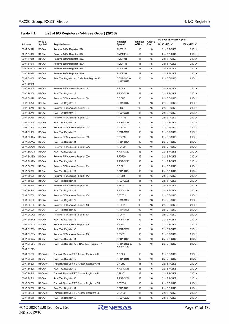
R01DS0261EJ0120 Rev.1.20 Page 71 of 170Sep 28, 2018
RX230 Group, RX231 Group 4. I/O Registers
000A 8494h RSCAN Receive Buffer Register 15BL RMTS15 16 16 2 or 3 PCLKB 2 ICLK
000A 8496h RSCAN Receive Buffer Register 15BH RMPTR15 16 16 2 or 3 PCLKB 2 ICLK
000A 8498h RSCAN Receive Buffer Register 15CL RMDF015 16 16 2 or 3 PCLKB 2 ICLK
000A 849Ah RSCAN Receive Buffer Register 15CH RMDF115 16 16 2 or 3 PCLKB 2 ICLK
000A 849Ch RSCAN Receive Buffer Register 15DL RMDF215 16 16 2 or 3 PCLKB 2 ICLK
000A 849Eh RSCAN Receive Buffer Register 15DH RMDF315 16 16 2 or 3 PCLKB 2 ICLK
000A 8580h to 000A 859Fh
RSCAN RAM Test Register 0 to RAM Test Register 15 RPGACC0 to RPGACC15
16 16 2 or 3 PCLKB 2 ICLK
000A 85A0h RSCAN Receive FIFO Access Register 0AL RFIDL0 16 16 2 or 3 PCLKB 2 ICLK
000A 85A0h RSCAN RAM Test Register 16 RPGACC16 16 16 2 or 3 PCLKB 2 ICLK
000A 85A2h RSCAN Receive FIFO Access Register 0AH RFIDH0 16 16 2 or 3 PCLKB 2 ICLK
000A 85A2h RSCAN RAM Test Register 17 RPGACC17 16 16 2 or 3 PCLKB 2 ICLK
000A 85A4h RSCAN Receive FIFO Access Register 0BL RFTS0 16 16 2 or 3 PCLKB 2 ICLK
000A 85A4h RSCAN RAM Test Register 18 RPGACC18 16 16 2 or 3 PCLKB 2 ICLK
000A 85A6h RSCAN Receive FIFO Access Register 0BH RFPTR0 16 16 2 or 3 PCLKB 2 ICLK
000A 85A6h RSCAN RAM Test Register 19 RPGACC19 16 16 2 or 3 PCLKB 2 ICLK
000A 85A8h RSCAN Receive FIFO Access Register 0CL RFDF00 16 16 2 or 3 PCLKB 2 ICLK
000A 85A8h RSCAN RAM Test Register 20 RPGACC20 16 16 2 or 3 PCLKB 2 ICLK
000A 85AAh RSCAN Receive FIFO Access Register 0CH RFDF10 16 16 2 or 3 PCLKB 2 ICLK
000A 85AAh RSCAN RAM Test Register 21 RPGACC21 16 16 2 or 3 PCLKB 2 ICLK
000A 85ACh RSCAN Receive FIFO Access Register 0DL RFDF20 16 16 2 or 3 PCLKB 2 ICLK
000A 85ACh RSCAN RAM Test Register 22 RPGACC22 16 16 2 or 3 PCLKB 2 ICLK
000A 85AEh RSCAN Receive FIFO Access Register 0DH RFDF30 16 16 2 or 3 PCLKB 2 ICLK
000A 85AEh RSCAN RAM Test Register 23 RPGACC23 16 16 2 or 3 PCLKB 2 ICLK
000A 85B0h RSCAN Receive FIFO Access Register 1AL RFIDL1 16 16 2 or 3 PCLKB 2 ICLK
000A 85B0h RSCAN RAM Test Register 24 RPGACC24 16 16 2 or 3 PCLKB 2 ICLK
000A 85B2h RSCAN Receive FIFO Access Register 1AH RFIDH1 16 16 2 or 3 PCLKB 2 ICLK
000A 85B2h RSCAN RAM Test Register 25 RPGACC25 16 16 2 or 3 PCLKB 2 ICLK
000A 85B4h RSCAN Receive FIFO Access Register 1BL RFTS1 16 16 2 or 3 PCLKB 2 ICLK
000A 85B4h RSCAN RAM Test Register 26 RPGACC26 16 16 2 or 3 PCLKB 2 ICLK
000A 85B6h RSCAN Receive FIFO Access Register 1BH RFPTR1 16 16 2 or 3 PCLKB 2 ICLK
000A 85B6h RSCAN RAM Test Register 27 RPGACC27 16 16 2 or 3 PCLKB 2 ICLK
000A 85B8h RSCAN Receive FIFO Access Register 1CL RFDF01 16 16 2 or 3 PCLKB 2 ICLK
000A 85B8h RSCAN RAM Test Register 28 RPGACC28 16 16 2 or 3 PCLKB 2 ICLK
000A 85BAh RSCAN Receive FIFO Access Register 1CH RFDF11 16 16 2 or 3 PCLKB 2 ICLK
000A 85BAh RSCAN RAM Test Register 29 RPGACC29 16 16 2 or 3 PCLKB 2 ICLK
000A 85BCh RSCAN Receive FIFO Access Register 1DL RFDF21 16 16 2 or 3 PCLKB 2 ICLK
000A 85BCh RSCAN RAM Test Register 30 RPGACC30 16 16 2 or 3 PCLKB 2 ICLK
000A 85BEh RSCAN Receive FIFO Access Register 1DH RFDF31 16 16 2 or 3 PCLKB 2 ICLK
000A 85BEh RSCAN RAM Test Register 31 RPGACC31 16 16 2 or 3 PCLKB 2 ICLK
000A 85C0h to 000A 85DEh
RSCAN RAM Test Register 32 to RAM Test Register 47 RPGACC32 to RPGACC47
16 16 2 or 3 PCLKB 2 ICLK
000A 85E0h RSCAN0 Transmit/Receive FIFO Access Register 0AL CFIDL0 16 16 2 or 3 PCLKB 2 ICLK
000A 85E0h RSCAN RAM Test Register 48 RPGACC48 16 16 2 or 3 PCLKB 2 ICLK
000A 85E2h RSCAN0 Transmit/Receive FIFO Access Register 0AH CFIDH0 16 16 2 or 3 PCLKB 2 ICLK
000A 85E2h RSCAN RAM Test Register 49 RPGACC49 16 16 2 or 3 PCLKB 2 ICLK
000A 85E4h RSCAN0 Transmit/Receive FIFO Access Register 0BL CFTS0 16 16 2 or 3 PCLKB 2 ICLK
000A 85E4h RSCAN RAM Test Register 50 RPGACC50 16 16 2 or 3 PCLKB 2 ICLK
000A 85E6h RSCAN0 Transmit/Receive FIFO Access Register 0BH CFPTR0 16 16 2 or 3 PCLKB 2 ICLK
000A 85E6h RSCAN RAM Test Register 51 RPGACC51 16 16 2 or 3 PCLKB 2 ICLK
000A 85E8h RSCAN0 Transmit/Receive FIFO Access Register 0CL CFDF00 16 16 2 or 3 PCLKB 2 ICLK
000A 85E8h RSCAN RAM Test Register 52 RPGACC52 16 16 2 or 3 PCLKB 2 ICLK
Table 4.1 List of I/O Registers (Address Order) (29/33)
AddressModule Symbol Register Name
Register Symbol
Number of Bits
Access Size
Number of Access Cycles
ICLK ≥ PCLK ICLK <PCLK

R01DS0261EJ0120 Rev.1.20 Page 72 of 170Sep 28, 2018
RX230 Group, RX231 Group 4. I/O Registers
000A 85EAh RSCAN0 Transmit/Receive FIFO Access Register 0CH CFDF10 16 16 2 or 3 PCLKB 2 ICLK
000A 85EAh RSCAN RAM Test Register 53 RPGACC53 16 16 2 or 3 PCLKB 2 ICLK
000A 85ECh RSCAN0 Transmit/Receive FIFO Access Register 0DL CFDF20 16 16 2 or 3 PCLKB 2 ICLK
000A 85ECh RSCAN RAM Test Register 54 RPGACC54 16 16 2 or 3 PCLKB 2 ICLK
000A 85EEh RSCAN0 Transmit/Receive FIFO Access Register 0DH CFDF30 16 16 2 or 3 PCLKB 2 ICLK
000A 85EEh RSCAN RAM Test Register 55 RPGACC55 16 16 2 or 3 PCLKB 2 ICLK
000A 85F0h to 000A 85FEh
RSCAN RAM Test Register 56 to RAM Test Register 63 RPGACC56 to RPGACC63
16 16 2 or 3 PCLKB 2 ICLK
000A 8600h RSCAN0 Transmit Buffer Register 0AL TMIDL0 16 16 2 or 3 PCLKB 2 ICLK
000A 8600h RSCAN RAM Test Register 64 RPGACC64 16 16 2 or 3 PCLKB 2 ICLK
000A 8602h RSCAN0 Transmit Buffer Register 0AH TMIDH0 16 16 2 or 3 PCLKB 2 ICLK
000A 8602h RSCAN RAM Test Register 65 RPGACC65 16 16 2 or 3 PCLKB 2 ICLK
000A 8604h RSCAN RAM Test Register 66 RPGACC66 16 16 2 or 3 PCLKB 2 ICLK
000A 8606h RSCAN0 Transmit Buffer Register 0BH TMPTR0 16 16 2 or 3 PCLKB 2 ICLK
000A 8606h RSCAN RAM Test Register 67 RPGACC67 16 16 2 or 3 PCLKB 2 ICLK
000A 8608h RSCAN0 Transmit Buffer Register 0CL TMDF00 16 16 2 or 3 PCLKB 2 ICLK
000A 8608h RSCAN RAM Test Register 68 RPGACC68 16 16 2 or 3 PCLKB 2 ICLK
000A 860Ah RSCAN0 Transmit Buffer Register 0CH TMDF10 16 16 2 or 3 PCLKB 2 ICLK
000A 860Ah RSCAN RAM Test Register 69 RPGACC69 16 16 2 or 3 PCLKB 2 ICLK
000A 860Ch RSCAN0 Transmit Buffer Register 0DL TMDF20 16 16 2 or 3 PCLKB 2 ICLK
000A 860Ch RSCAN RAM Test Register 70 RPGACC70 16 16 2 or 3 PCLKB 2 ICLK
000A 860Eh RSCAN0 Transmit Buffer Register 0DH TMDF30 16 16 2 or 3 PCLKB 2 ICLK
000A 860Eh RSCAN RAM Test Register 71 RPGACC71 16 16 2 or 3 PCLKB 2 ICLK
000A 8610h RSCAN0 Transmit Buffer Register 1AL TMIDL1 16 16 2 or 3 PCLKB 2 ICLK
000A 8610h RSCAN RAM Test Register 72 RPGACC72 16 16 2 or 3 PCLKB 2 ICLK
000A 8612h RSCAN0 Transmit Buffer Register 1AH TMIDH1 16 16 2 or 3 PCLKB 2 ICLK
000A 8612h RSCAN RAM Test Register 73 RPGACC73 16 16 2 or 3 PCLKB 2 ICLK
000A 8614h RSCAN RAM Test Register 74 RPGACC74 16 16 2 or 3 PCLKB 2 ICLK
000A 8616h RSCAN0 Transmit Buffer Register 1BH TMPTR1 16 16 2 or 3 PCLKB 2 ICLK
000A 8616h RSCAN RAM Test Register 75 RPGACC75 16 16 2 or 3 PCLKB 2 ICLK
000A 8618h RSCAN0 Transmit Buffer Register 1CL TMDF01 16 16 2 or 3 PCLKB 2 ICLK
000A 8618h RSCAN RAM Test Register 76 RPGACC76 16 16 2 or 3 PCLKB 2 ICLK
000A 861Ah RSCAN0 Transmit Buffer Register 1CH TMDF11 16 16 2 or 3 PCLKB 2 ICLK
000A 861Ah RSCAN RAM Test Register 77 RPGACC77 16 16 2 or 3 PCLKB 2 ICLK
000A 861Ch RSCAN0 Transmit Buffer Register 1DL TMDF21 16 16 2 or 3 PCLKB 2 ICLK
000A 861Ch RSCAN RAM Test Register 78 RPGACC78 16 16 2 or 3 PCLKB 2 ICLK
000A 861Eh RSCAN0 Transmit Buffer Register 1DH TMDF31 16 16 2 or 3 PCLKB 2 ICLK
000A 861Eh RSCAN RAM Test Register 79 RPGACC79 16 16 2 or 3 PCLKB 2 ICLK
000A 8620h RSCAN0 Transmit Buffer Register 2AL TMIDL2 16 16 2 or 3 PCLKB 2 ICLK
000A 8620h RSCAN RAM Test Register 80 RPGACC80 16 16 2 or 3 PCLKB 2 ICLK
000A 8622h RSCAN0 Transmit Buffer Register 2AH TMIDH2 16 16 2 or 3 PCLKB 2 ICLK
000A 8622h RSCAN RAM Test Register 81 RPGACC81 16 16 2 or 3 PCLKB 2 ICLK
000A 8624h RSCAN RAM Test Register 82 RPGACC82 16 16 2 or 3 PCLKB 2 ICLK
000A 8626h RSCAN0 Transmit Buffer Register 2BH TMPTR2 16 16 2 or 3 PCLKB 2 ICLK
000A 8626h RSCAN RAM Test Register 83 RPGACC83 16 16 2 or 3 PCLKB 2 ICLK
000A 8628h RSCAN0 Transmit Buffer Register 2CL TMDF02 16 16 2 or 3 PCLKB 2 ICLK
000A 8628h RSCAN RAM Test Register 84 RPGACC84 16 16 2 or 3 PCLKB 2 ICLK
000A 862Ah RSCAN0 Transmit Buffer Register 2CH TMDF12 16 16 2 or 3 PCLKB 2 ICLK
000A 862Ah RSCAN RAM Test Register 85 RPGACC85 16 16 2 or 3 PCLKB 2 ICLK
000A 862Ch RSCAN0 Transmit Buffer Register 2DL TMDF22 16 16 2 or 3 PCLKB 2 ICLK
000A 862Ch RSCAN RAM Test Register 86 RPGACC86 16 16 2 or 3 PCLKB 2 ICLK
000A 862Eh RSCAN0 Transmit Buffer Register 2DH TMDF32 16 16 2 or 3 PCLKB 2 ICLK
Table 4.1 List of I/O Registers (Address Order) (30/33)
AddressModule Symbol Register Name
Register Symbol
Number of Bits
Access Size
Number of Access Cycles
ICLK ≥ PCLK ICLK <PCLK
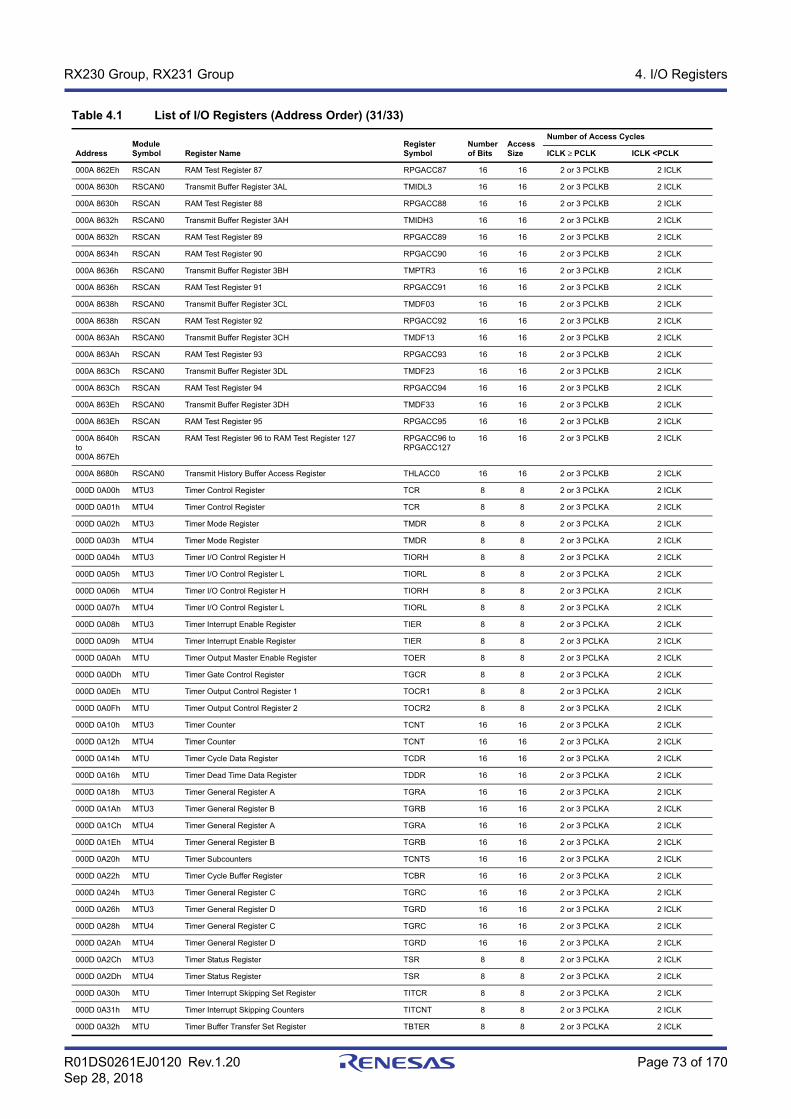
R01DS0261EJ0120 Rev.1.20 Page 73 of 170Sep 28, 2018
RX230 Group, RX231 Group 4. I/O Registers
000A 862Eh RSCAN RAM Test Register 87 RPGACC87 16 16 2 or 3 PCLKB 2 ICLK
000A 8630h RSCAN0 Transmit Buffer Register 3AL TMIDL3 16 16 2 or 3 PCLKB 2 ICLK
000A 8630h RSCAN RAM Test Register 88 RPGACC88 16 16 2 or 3 PCLKB 2 ICLK
000A 8632h RSCAN0 Transmit Buffer Register 3AH TMIDH3 16 16 2 or 3 PCLKB 2 ICLK
000A 8632h RSCAN RAM Test Register 89 RPGACC89 16 16 2 or 3 PCLKB 2 ICLK
000A 8634h RSCAN RAM Test Register 90 RPGACC90 16 16 2 or 3 PCLKB 2 ICLK
000A 8636h RSCAN0 Transmit Buffer Register 3BH TMPTR3 16 16 2 or 3 PCLKB 2 ICLK
000A 8636h RSCAN RAM Test Register 91 RPGACC91 16 16 2 or 3 PCLKB 2 ICLK
000A 8638h RSCAN0 Transmit Buffer Register 3CL TMDF03 16 16 2 or 3 PCLKB 2 ICLK
000A 8638h RSCAN RAM Test Register 92 RPGACC92 16 16 2 or 3 PCLKB 2 ICLK
000A 863Ah RSCAN0 Transmit Buffer Register 3CH TMDF13 16 16 2 or 3 PCLKB 2 ICLK
000A 863Ah RSCAN RAM Test Register 93 RPGACC93 16 16 2 or 3 PCLKB 2 ICLK
000A 863Ch RSCAN0 Transmit Buffer Register 3DL TMDF23 16 16 2 or 3 PCLKB 2 ICLK
000A 863Ch RSCAN RAM Test Register 94 RPGACC94 16 16 2 or 3 PCLKB 2 ICLK
000A 863Eh RSCAN0 Transmit Buffer Register 3DH TMDF33 16 16 2 or 3 PCLKB 2 ICLK
000A 863Eh RSCAN RAM Test Register 95 RPGACC95 16 16 2 or 3 PCLKB 2 ICLK
000A 8640h to 000A 867Eh
RSCAN RAM Test Register 96 to RAM Test Register 127 RPGACC96 to RPGACC127
16 16 2 or 3 PCLKB 2 ICLK
000A 8680h RSCAN0 Transmit History Buffer Access Register THLACC0 16 16 2 or 3 PCLKB 2 ICLK
000D 0A00h MTU3 Timer Control Register TCR 8 8 2 or 3 PCLKA 2 ICLK
000D 0A01h MTU4 Timer Control Register TCR 8 8 2 or 3 PCLKA 2 ICLK
000D 0A02h MTU3 Timer Mode Register TMDR 8 8 2 or 3 PCLKA 2 ICLK
000D 0A03h MTU4 Timer Mode Register TMDR 8 8 2 or 3 PCLKA 2 ICLK
000D 0A04h MTU3 Timer I/O Control Register H TIORH 8 8 2 or 3 PCLKA 2 ICLK
000D 0A05h MTU3 Timer I/O Control Register L TIORL 8 8 2 or 3 PCLKA 2 ICLK
000D 0A06h MTU4 Timer I/O Control Register H TIORH 8 8 2 or 3 PCLKA 2 ICLK
000D 0A07h MTU4 Timer I/O Control Register L TIORL 8 8 2 or 3 PCLKA 2 ICLK
000D 0A08h MTU3 Timer Interrupt Enable Register TIER 8 8 2 or 3 PCLKA 2 ICLK
000D 0A09h MTU4 Timer Interrupt Enable Register TIER 8 8 2 or 3 PCLKA 2 ICLK
000D 0A0Ah MTU Timer Output Master Enable Register TOER 8 8 2 or 3 PCLKA 2 ICLK
000D 0A0Dh MTU Timer Gate Control Register TGCR 8 8 2 or 3 PCLKA 2 ICLK
000D 0A0Eh MTU Timer Output Control Register 1 TOCR1 8 8 2 or 3 PCLKA 2 ICLK
000D 0A0Fh MTU Timer Output Control Register 2 TOCR2 8 8 2 or 3 PCLKA 2 ICLK
000D 0A10h MTU3 Timer Counter TCNT 16 16 2 or 3 PCLKA 2 ICLK
000D 0A12h MTU4 Timer Counter TCNT 16 16 2 or 3 PCLKA 2 ICLK
000D 0A14h MTU Timer Cycle Data Register TCDR 16 16 2 or 3 PCLKA 2 ICLK
000D 0A16h MTU Timer Dead Time Data Register TDDR 16 16 2 or 3 PCLKA 2 ICLK
000D 0A18h MTU3 Timer General Register A TGRA 16 16 2 or 3 PCLKA 2 ICLK
000D 0A1Ah MTU3 Timer General Register B TGRB 16 16 2 or 3 PCLKA 2 ICLK
000D 0A1Ch MTU4 Timer General Register A TGRA 16 16 2 or 3 PCLKA 2 ICLK
000D 0A1Eh MTU4 Timer General Register B TGRB 16 16 2 or 3 PCLKA 2 ICLK
000D 0A20h MTU Timer Subcounters TCNTS 16 16 2 or 3 PCLKA 2 ICLK
000D 0A22h MTU Timer Cycle Buffer Register TCBR 16 16 2 or 3 PCLKA 2 ICLK
000D 0A24h MTU3 Timer General Register C TGRC 16 16 2 or 3 PCLKA 2 ICLK
000D 0A26h MTU3 Timer General Register D TGRD 16 16 2 or 3 PCLKA 2 ICLK
000D 0A28h MTU4 Timer General Register C TGRC 16 16 2 or 3 PCLKA 2 ICLK
000D 0A2Ah MTU4 Timer General Register D TGRD 16 16 2 or 3 PCLKA 2 ICLK
000D 0A2Ch MTU3 Timer Status Register TSR 8 8 2 or 3 PCLKA 2 ICLK
000D 0A2Dh MTU4 Timer Status Register TSR 8 8 2 or 3 PCLKA 2 ICLK
000D 0A30h MTU Timer Interrupt Skipping Set Register TITCR 8 8 2 or 3 PCLKA 2 ICLK
000D 0A31h MTU Timer Interrupt Skipping Counters TITCNT 8 8 2 or 3 PCLKA 2 ICLK
000D 0A32h MTU Timer Buffer Transfer Set Register TBTER 8 8 2 or 3 PCLKA 2 ICLK
Table 4.1 List of I/O Registers (Address Order) (31/33)
AddressModule Symbol Register Name
Register Symbol
Number of Bits
Access Size
Number of Access Cycles
ICLK ≥ PCLK ICLK <PCLK
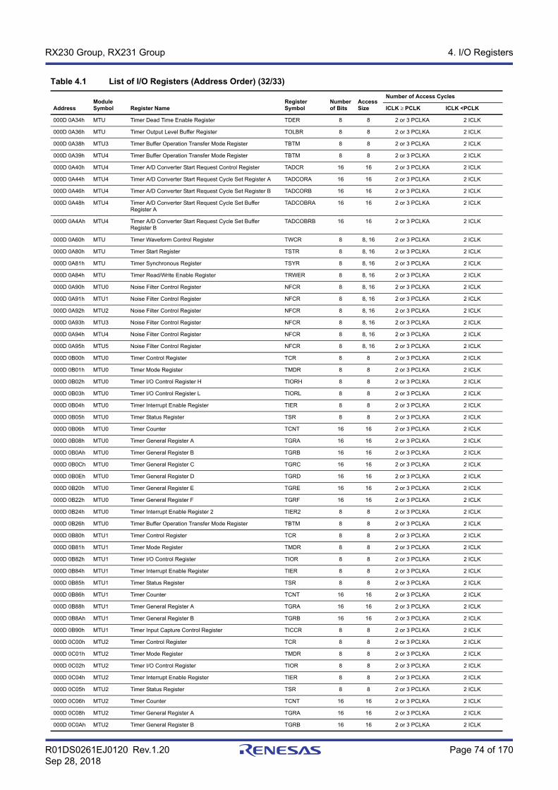
R01DS0261EJ0120 Rev.1.20 Page 74 of 170Sep 28, 2018
RX230 Group, RX231 Group 4. I/O Registers
000D 0A34h MTU Timer Dead Time Enable Register TDER 8 8 2 or 3 PCLKA 2 ICLK
000D 0A36h MTU Timer Output Level Buffer Register TOLBR 8 8 2 or 3 PCLKA 2 ICLK
000D 0A38h MTU3 Timer Buffer Operation Transfer Mode Register TBTM 8 8 2 or 3 PCLKA 2 ICLK
000D 0A39h MTU4 Timer Buffer Operation Transfer Mode Register TBTM 8 8 2 or 3 PCLKA 2 ICLK
000D 0A40h MTU4 Timer A/D Converter Start Request Control Register TADCR 16 16 2 or 3 PCLKA 2 ICLK
000D 0A44h MTU4 Timer A/D Converter Start Request Cycle Set Register A TADCORA 16 16 2 or 3 PCLKA 2 ICLK
000D 0A46h MTU4 Timer A/D Converter Start Request Cycle Set Register B TADCORB 16 16 2 or 3 PCLKA 2 ICLK
000D 0A48h MTU4 Timer A/D Converter Start Request Cycle Set Buffer Register A
TADCOBRA 16 16 2 or 3 PCLKA 2 ICLK
000D 0A4Ah MTU4 Timer A/D Converter Start Request Cycle Set Buffer Register B
TADCOBRB 16 16 2 or 3 PCLKA 2 ICLK
000D 0A60h MTU Timer Waveform Control Register TWCR 8 8, 16 2 or 3 PCLKA 2 ICLK
000D 0A80h MTU Timer Start Register TSTR 8 8, 16 2 or 3 PCLKA 2 ICLK
000D 0A81h MTU Timer Synchronous Register TSYR 8 8, 16 2 or 3 PCLKA 2 ICLK
000D 0A84h MTU Timer Read/Write Enable Register TRWER 8 8, 16 2 or 3 PCLKA 2 ICLK
000D 0A90h MTU0 Noise Filter Control Register NFCR 8 8, 16 2 or 3 PCLKA 2 ICLK
000D 0A91h MTU1 Noise Filter Control Register NFCR 8 8, 16 2 or 3 PCLKA 2 ICLK
000D 0A92h MTU2 Noise Filter Control Register NFCR 8 8, 16 2 or 3 PCLKA 2 ICLK
000D 0A93h MTU3 Noise Filter Control Register NFCR 8 8, 16 2 or 3 PCLKA 2 ICLK
000D 0A94h MTU4 Noise Filter Control Register NFCR 8 8, 16 2 or 3 PCLKA 2 ICLK
000D 0A95h MTU5 Noise Filter Control Register NFCR 8 8, 16 2 or 3 PCLKA 2 ICLK
000D 0B00h MTU0 Timer Control Register TCR 8 8 2 or 3 PCLKA 2 ICLK
000D 0B01h MTU0 Timer Mode Register TMDR 8 8 2 or 3 PCLKA 2 ICLK
000D 0B02h MTU0 Timer I/O Control Register H TIORH 8 8 2 or 3 PCLKA 2 ICLK
000D 0B03h MTU0 Timer I/O Control Register L TIORL 8 8 2 or 3 PCLKA 2 ICLK
000D 0B04h MTU0 Timer Interrupt Enable Register TIER 8 8 2 or 3 PCLKA 2 ICLK
000D 0B05h MTU0 Timer Status Register TSR 8 8 2 or 3 PCLKA 2 ICLK
000D 0B06h MTU0 Timer Counter TCNT 16 16 2 or 3 PCLKA 2 ICLK
000D 0B08h MTU0 Timer General Register A TGRA 16 16 2 or 3 PCLKA 2 ICLK
000D 0B0Ah MTU0 Timer General Register B TGRB 16 16 2 or 3 PCLKA 2 ICLK
000D 0B0Ch MTU0 Timer General Register C TGRC 16 16 2 or 3 PCLKA 2 ICLK
000D 0B0Eh MTU0 Timer General Register D TGRD 16 16 2 or 3 PCLKA 2 ICLK
000D 0B20h MTU0 Timer General Register E TGRE 16 16 2 or 3 PCLKA 2 ICLK
000D 0B22h MTU0 Timer General Register F TGRF 16 16 2 or 3 PCLKA 2 ICLK
000D 0B24h MTU0 Timer Interrupt Enable Register 2 TIER2 8 8 2 or 3 PCLKA 2 ICLK
000D 0B26h MTU0 Timer Buffer Operation Transfer Mode Register TBTM 8 8 2 or 3 PCLKA 2 ICLK
000D 0B80h MTU1 Timer Control Register TCR 8 8 2 or 3 PCLKA 2 ICLK
000D 0B81h MTU1 Timer Mode Register TMDR 8 8 2 or 3 PCLKA 2 ICLK
000D 0B82h MTU1 Timer I/O Control Register TIOR 8 8 2 or 3 PCLKA 2 ICLK
000D 0B84h MTU1 Timer Interrupt Enable Register TIER 8 8 2 or 3 PCLKA 2 ICLK
000D 0B85h MTU1 Timer Status Register TSR 8 8 2 or 3 PCLKA 2 ICLK
000D 0B86h MTU1 Timer Counter TCNT 16 16 2 or 3 PCLKA 2 ICLK
000D 0B88h MTU1 Timer General Register A TGRA 16 16 2 or 3 PCLKA 2 ICLK
000D 0B8Ah MTU1 Timer General Register B TGRB 16 16 2 or 3 PCLKA 2 ICLK
000D 0B90h MTU1 Timer Input Capture Control Register TICCR 8 8 2 or 3 PCLKA 2 ICLK
000D 0C00h MTU2 Timer Control Register TCR 8 8 2 or 3 PCLKA 2 ICLK
000D 0C01h MTU2 Timer Mode Register TMDR 8 8 2 or 3 PCLKA 2 ICLK
000D 0C02h MTU2 Timer I/O Control Register TIOR 8 8 2 or 3 PCLKA 2 ICLK
000D 0C04h MTU2 Timer Interrupt Enable Register TIER 8 8 2 or 3 PCLKA 2 ICLK
000D 0C05h MTU2 Timer Status Register TSR 8 8 2 or 3 PCLKA 2 ICLK
000D 0C06h MTU2 Timer Counter TCNT 16 16 2 or 3 PCLKA 2 ICLK
000D 0C08h MTU2 Timer General Register A TGRA 16 16 2 or 3 PCLKA 2 ICLK
000D 0C0Ah MTU2 Timer General Register B TGRB 16 16 2 or 3 PCLKA 2 ICLK
Table 4.1 List of I/O Registers (Address Order) (32/33)
AddressModule Symbol Register Name
Register Symbol
Number of Bits
Access Size
Number of Access Cycles
ICLK ≥ PCLK ICLK <PCLK
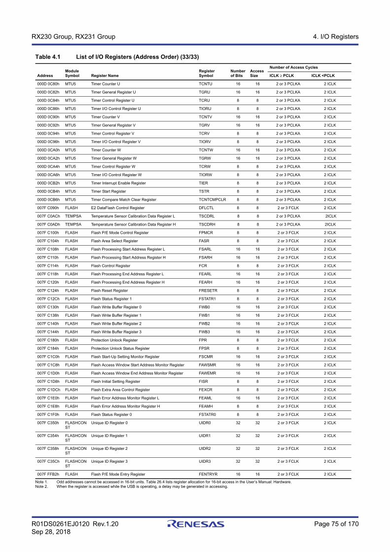
R01DS0261EJ0120 Rev.1.20 Page 75 of 170Sep 28, 2018
RX230 Group, RX231 Group 4. I/O Registers
Note 1. Odd addresses cannot be accessed in 16-bit units. Table 26.4 lists register allocation for 16-bit access in the User’s Manual: Hardware.Note 2. When the register is accessed while the USB is operating, a delay may be generated in accessing.
000D 0C80h MTU5 Timer Counter U TCNTU 16 16 2 or 3 PCLKA 2 ICLK
000D 0C82h MTU5 Timer General Register U TGRU 16 16 2 or 3 PCLKA 2 ICLK
000D 0C84h MTU5 Timer Control Register U TCRU 8 8 2 or 3 PCLKA 2 ICLK
000D 0C86h MTU5 Timer I/O Control Register U TIORU 8 8 2 or 3 PCLKA 2 ICLK
000D 0C90h MTU5 Timer Counter V TCNTV 16 16 2 or 3 PCLKA 2 ICLK
000D 0C92h MTU5 Timer General Register V TGRV 16 16 2 or 3 PCLKA 2 ICLK
000D 0C94h MTU5 Timer Control Register V TCRV 8 8 2 or 3 PCLKA 2 ICLK
000D 0C96h MTU5 Timer I/O Control Register V TIORV 8 8 2 or 3 PCLKA 2 ICLK
000D 0CA0h MTU5 Timer Counter W TCNTW 16 16 2 or 3 PCLKA 2 ICLK
000D 0CA2h MTU5 Timer General Register W TGRW 16 16 2 or 3 PCLKA 2 ICLK
000D 0CA4h MTU5 Timer Control Register W TCRW 8 8 2 or 3 PCLKA 2 ICLK
000D 0CA6h MTU5 Timer I/O Control Register W TIORW 8 8 2 or 3 PCLKA 2 ICLK
000D 0CB2h MTU5 Timer Interrupt Enable Register TIER 8 8 2 or 3 PCLKA 2 ICLK
000D 0CB4h MTU5 Timer Start Register TSTR 8 8 2 or 3 PCLKA 2 ICLK
000D 0CB6h MTU5 Timer Compare Match Clear Register TCNTCMPCLR 8 8 2 or 3 PCLKA 2 ICLK
007F C090h FLASH E2 DataFlash Control Register DFLCTL 8 8 2 or 3 FCLK 2 ICLK
007F C0ACh TEMPSA Temperature Sensor Calibration Data Register L TSCDRL 8 8 2 or 3 PCLKA 2ICLK
007F C0ADh TEMPSA Temperature Sensor Calibration Data Register H TSCDRH 8 8 2 or 3 PCLKA 2ICLK
007F C100h FLASH Flash P/E Mode Control Register FPMCR 8 8 2 or 3 FCLK 2 ICLK
007F C104h FLASH Flash Area Select Register FASR 8 8 2 or 3 FCLK 2 ICLK
007F C108h FLASH Flash Processing Start Address Register L FSARL 16 16 2 or 3 FCLK 2 ICLK
007F C110h FLASH Flash Processing Start Address Register H FSARH 16 16 2 or 3 FCLK 2 ICLK
007F C114h FLASH Flash Control Register FCR 8 8 2 or 3 FCLK 2 ICLK
007F C118h FLASH Flash Processing End Address Register L FEARL 16 16 2 or 3 FCLK 2 ICLK
007F C120h FLASH Flash Processing End Address Register H FEARH 16 16 2 or 3 FCLK 2 ICLK
007F C124h FLASH Flash Reset Register FRESETR 8 8 2 or 3 FCLK 2 ICLK
007F C12Ch FLASH Flash Status Register 1 FSTATR1 8 8 2 or 3 FCLK 2 ICLK
007F C130h FLASH Flash Write Buffer Register 0 FWB0 16 16 2 or 3 FCLK 2 ICLK
007F C138h FLASH Flash Write Buffer Register 1 FWB1 16 16 2 or 3 FCLK 2 ICLK
007F C140h FLASH Flash Write Buffer Register 2 FWB2 16 16 2 or 3 FCLK 2 ICLK
007F C144h FLASH Flash Write Buffer Register 3 FWB3 16 16 2 or 3 FCLK 2 ICLK
007F C180h FLASH Protection Unlock Register FPR 8 8 2 or 3 FCLK 2 ICLK
007F C184h FLASH Protection Unlock Status Register FPSR 8 8 2 or 3 FCLK 2 ICLK
007F C1C0h FLASH Flash Start-Up Setting Monitor Register FSCMR 16 16 2 or 3 FCLK 2 ICLK
007F C1C8h FLASH Flash Access Window Start Address Monitor Register FAWSMR 16 16 2 or 3 FCLK 2 ICLK
007F C1D0h FLASH Flash Access Window End Address Monitor Register FAWEMR 16 16 2 or 3 FCLK 2 ICLK
007F C1D8h FLASH Flash Initial Setting Register FISR 8 8 2 or 3 FCLK 2 ICLK
007F C1DCh FLASH Flash Extra Area Control Register FEXCR 8 8 2 or 3 FCLK 2 ICLK
007F C1E0h FLASH Flash Error Address Monitor Register L FEAML 16 16 2 or 3 FCLK 2 ICLK
007F C1E8h FLASH Flash Error Address Monitor Register H FEAMH 8 8 2 or 3 FCLK 2 ICLK
007F C1F0h FLASH Flash Status Register 0 FSTATR0 8 8 2 or 3 FCLK 2 ICLK
007F C350h FLASHCONST
Unique ID Register 0 UIDR0 32 32 2 or 3 FCLK 2 ICLK
007F C354h FLASHCONST
Unique ID Register 1 UIDR1 32 32 2 or 3 FCLK 2 ICLK
007F C358h FLASHCONST
Unique ID Register 2 UIDR2 32 32 2 or 3 FCLK 2 ICLK
007F C35Ch FLASHCONST
Unique ID Register 3 UIDR3 32 32 2 or 3 FCLK 2 ICLK
007F FFB2h FLASH Flash P/E Mode Entry Register FENTRYR 16 16 2 or 3 FCLK 2 ICLK
Table 4.1 List of I/O Registers (Address Order) (33/33)
AddressModule Symbol Register Name
Register Symbol
Number of Bits
Access Size
Number of Access Cycles
ICLK ≥ PCLK ICLK <PCLK
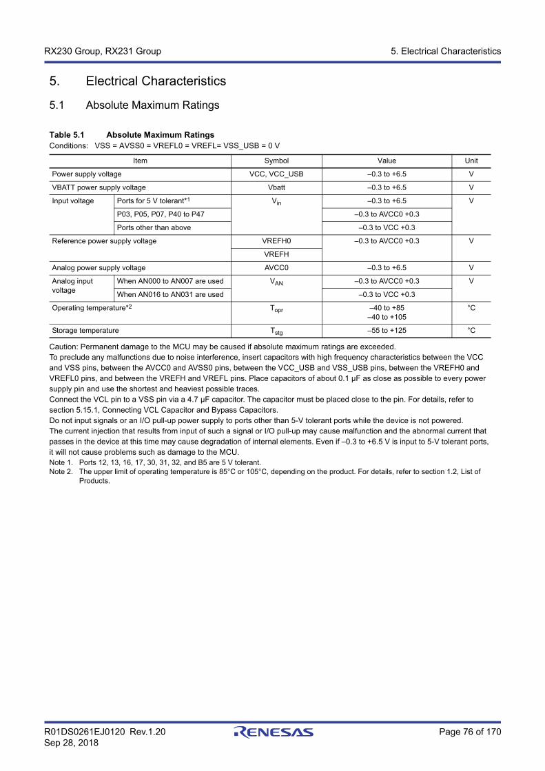
R01DS0261EJ0120 Rev.1.20 Page 76 of 170Sep 28, 2018
RX230 Group, RX231 Group 5. Electrical Characteristics
5. Electrical Characteristics
5.1 Absolute Maximum Ratings
Caution: Permanent damage to the MCU may be caused if absolute maximum ratings are exceeded.To preclude any malfunctions due to noise interference, insert capacitors with high frequency characteristics between the VCC and VSS pins, between the AVCC0 and AVSS0 pins, between the VCC_USB and VSS_USB pins, between the VREFH0 and VREFL0 pins, and between the VREFH and VREFL pins. Place capacitors of about 0.1 μF as close as possible to every power supply pin and use the shortest and heaviest possible traces.Connect the VCL pin to a VSS pin via a 4.7 μF capacitor. The capacitor must be placed close to the pin. For details, refer to section 5.15.1, Connecting VCL Capacitor and Bypass Capacitors.Do not input signals or an I/O pull-up power supply to ports other than 5-V tolerant ports while the device is not powered.The current injection that results from input of such a signal or I/O pull-up may cause malfunction and the abnormal current that passes in the device at this time may cause degradation of internal elements. Even if –0.3 to +6.5 V is input to 5-V tolerant ports, it will not cause problems such as damage to the MCU.Note 1. Ports 12, 13, 16, 17, 30, 31, 32, and B5 are 5 V tolerant.Note 2. The upper limit of operating temperature is 85°C or 105°C, depending on the product. For details, refer to section 1.2, List of
Products.
Table 5.1 Absolute Maximum RatingsConditions: VSS = AVSS0 = VREFL0 = VREFL= VSS_USB = 0 V
Item Symbol Value Unit
Power supply voltage VCC, VCC_USB –0.3 to +6.5 V
VBATT power supply voltage Vbatt –0.3 to +6.5 V
Input voltage Ports for 5 V tolerant*1 Vin –0.3 to +6.5 V
P03, P05, P07, P40 to P47 –0.3 to AVCC0 +0.3
Ports other than above –0.3 to VCC +0.3
Reference power supply voltage VREFH0 –0.3 to AVCC0 +0.3 V
VREFH
Analog power supply voltage AVCC0 –0.3 to +6.5 V
Analog input voltage
When AN000 to AN007 are used VAN –0.3 to AVCC0 +0.3 V
When AN016 to AN031 are used –0.3 to VCC +0.3
Operating temperature*2 Topr –40 to +85–40 to +105
°C
Storage temperature Tstg –55 to +125 °C

R01DS0261EJ0120 Rev.1.20 Page 77 of 170Sep 28, 2018
RX230 Group, RX231 Group 5. Electrical Characteristics
Note 1. Use AVCC0 and VCC under the following conditions: AVCC0 and VCC can be set individually within the operating range when VCC ≥ 2.0 VAVCC0 = VCC when VCC ˂ 2.0 V
Note 2. When powering on the VCC and AVCC0 pins, power them on at the same time or the VCC pin first and then the AVCC0 pin.
Table 5.2 Recommended Operating Voltage Conditions
Item Symbol Conditions Min. Typ. Max. Unit
Power supply voltages VCC*1, *2 When USB is not used 1.8 — 5.5 V
When USB is usedWhen USB regulator is not used
3.0 — 3.6
When USB is usedWhen USB regulator is used
4.0 — 5.5
VSS — 0 —
USB power supply voltages VCC_USB When USB regulator is not used — VCC — V
VSS_USB — 0 —
VBATT power supply voltage VBATT 1.8 — 5.5 V
Analog power supply voltages AVCC0*1, *2 1.8 — 5.5 V
AVSS0 — 0 —
VREFH0 1.8 — AVCC0
VREFL0 — 0 —
VREFH 1.8 — AVCC0
VREFL — 0 —
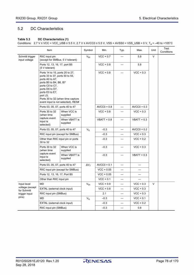
R01DS0261EJ0120 Rev.1.20 Page 78 of 170Sep 28, 2018
RX230 Group, RX231 Group 5. Electrical Characteristics
5.2 DC Characteristics
Table 5.3 DC Characteristics (1)Conditions: 2.7 V ≤ VCC = VCC_USB ≤ 5.5 V, 2.7 V ≤ AVCC0 ≤ 5.5 V, VSS = AVSS0 = VSS_USB = 0 V, Ta = –40 to +105°C
Item Symbol Min. Typ. Max. Unit Test Conditions
Schmitt trigger input voltage
RIIC input pin(except for SMBus, 5 V tolerant)
VIH VCC × 0.7 — 5.8 V
Ports 12, 13, 16, 17, port B5(5 V tolerant)
VCC × 0.8 — 5.8
Ports 14 to 15, ports 20 to 27,ports 33 to 37, ports 50 to 55,ports A0 to A7,ports B0 to B4, B6, B7ports C0 to C7,ports D0 to D7,ports E0 to E7,port J3,Ports 30 to 32 (when time capture event input is not selected), RES#
VCC × 0.8 — VCC + 0.3
Ports 03, 05, 07, ports 40 to 47 AVCC0 × 0.8 — AVCC0 + 0.3
Ports 30 to 32(when time capture event input is selected)
When VCC is supplied
VCC × 0.8 — VCC + 0.3
When VBATT is supplied
VBATT × 0.8 — VBATT + 0.3
Ports 03, 05, 07, ports 40 to 47 VIL –0.3 — AVCC0 × 0.2
RIIC input pin (except for SMBus) –0.3 — VCC × 0.3
Other than RIIC input pin or ports 30 to 32
–0.3 — VCC × 0.2
Ports 30 to 32(when time capture event input is selected)
When VCC is supplied
–0.3 — VCC × 0.3
When VBATT is supplied
–0.3 — VBATT × 0.3
Ports 03, 05, 07, ports 40 to 47 ΔVT AVCC0 × 0.1 — —
RIIC input pin (except for SMBus) VCC × 0.05 — —
Ports 12, 13, 16, 17, Port B5 VCC × 0.05 — —
Other than RIIC input pin VCC × 0.1 — —
Input level voltage (except for Schmitt trigger input pins)
MD VIH VCC × 0.9 — VCC + 0.3 V
EXTAL (external clock input) VCC × 0.8 — VCC + 0.3
RIIC input pin (SMBus) 2.1 — VCC + 0.3
MD VIL –0.3 — VCC × 0.1
EXTAL (external clock input) –0.3 — VCC × 0.2
RIIC input pin (SMBus) –0.3 — 0.8
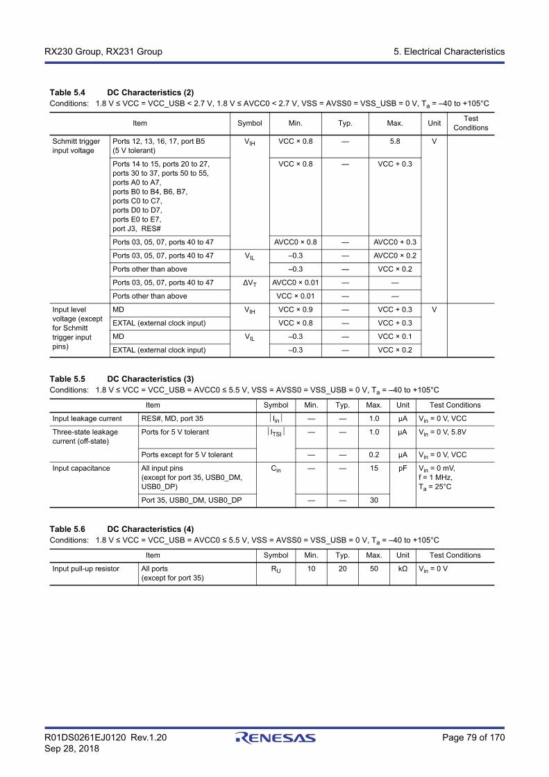
R01DS0261EJ0120 Rev.1.20 Page 79 of 170Sep 28, 2018
RX230 Group, RX231 Group 5. Electrical Characteristics
Table 5.4 DC Characteristics (2)Conditions: 1.8 V ≤ VCC = VCC_USB < 2.7 V, 1.8 V ≤ AVCC0 < 2.7 V, VSS = AVSS0 = VSS_USB = 0 V, Ta = –40 to +105°C
Item Symbol Min. Typ. Max. Unit Test Conditions
Schmitt trigger input voltage
Ports 12, 13, 16, 17, port B5(5 V tolerant)
VIH VCC × 0.8 — 5.8 V
Ports 14 to 15, ports 20 to 27,ports 30 to 37, ports 50 to 55,ports A0 to A7,ports B0 to B4, B6, B7,ports C0 to C7,ports D0 to D7,ports E0 to E7,port J3, RES#
VCC × 0.8 — VCC + 0.3
Ports 03, 05, 07, ports 40 to 47 AVCC0 × 0.8 — AVCC0 + 0.3
Ports 03, 05, 07, ports 40 to 47 VIL –0.3 — AVCC0 × 0.2
Ports other than above –0.3 — VCC × 0.2
Ports 03, 05, 07, ports 40 to 47 ΔVT AVCC0 × 0.01 — —
Ports other than above VCC × 0.01 — —
Input level voltage (except for Schmitt trigger input pins)
MD VIH VCC × 0.9 — VCC + 0.3 V
EXTAL (external clock input) VCC × 0.8 — VCC + 0.3
MD VIL –0.3 — VCC × 0.1
EXTAL (external clock input) –0.3 — VCC × 0.2
Table 5.5 DC Characteristics (3)Conditions: 1.8 V ≤ VCC = VCC_USB = AVCC0 ≤ 5.5 V, VSS = AVSS0 = VSS_USB = 0 V, Ta = –40 to +105°C
Item Symbol Min. Typ. Max. Unit Test Conditions
Input leakage current RES#, MD, port 35 ⏐Iin⏐ — — 1.0 μA Vin = 0 V, VCC
Three-state leakage current (off-state)
Ports for 5 V tolerant ⏐ITSI⏐ — — 1.0 μA Vin = 0 V, 5.8V
Ports except for 5 V tolerant — — 0.2 μA Vin = 0 V, VCC
Input capacitance All input pins(except for port 35, USB0_DM, USB0_DP)
Cin — — 15 pF Vin = 0 mV, f = 1 MHz, Ta = 25°C
Port 35, USB0_DM, USB0_DP — — 30
Table 5.6 DC Characteristics (4)Conditions: 1.8 V ≤ VCC = VCC_USB = AVCC0 ≤ 5.5 V, VSS = AVSS0 = VSS_USB = 0 V, Ta = –40 to +105°C
Item Symbol Min. Typ. Max. Unit Test Conditions
Input pull-up resistor All ports(except for port 35)
RU 10 20 50 kΩ Vin = 0 V

R01DS0261EJ0120 Rev.1.20 Page 80 of 170Sep 28, 2018
RX230 Group, RX231 Group 5. Electrical Characteristics
Table 5.7 DC Characteristics (5)Conditions: 1.8 V ≤ VCC = VCC_USB = AVCC0 ≤ 5.5 V, VSS = AVSS0 = VSS_USB = 0 V, Ta = –40 to +105°C
Item Symbol Typ.*4 Max. Unit Test
Conditions
Supply current*1
High-speed operating mode
Normal operating mode
No peripheral operation*2
ICLK = 54 MHz ICC 6.5 — mA
ICLK = 32 MHz 4.1 —
ICLK = 16 MHz 2.9 —
ICLK = 8 MHz 2.2 —
ICLK = 4 MHz 1.9 —
All peripheral operation: Normal
ICLK = 54 MHz*11 26.5 —
ICLK = 32 MHz*3 21.0 —
ICLK = 16 MHz*3 11.8 —
ICLK = 8 MHz*3 6.6 —
ICLK = 4 MHz*3 4.2 —
All peripheral operation: Max.
ICLK = 54 MHz*11 — 53.3
ICLK = 32 MHz*3 — 40.8
Increase due to operation of the Trusted Secure IP
PCLKB = 32 MHz — 2
Sleep mode No peripheral operation*2
ICLK = 54 MHz 3.5 —
ICLK = 32 MHz 2.4 —
ICLK = 16 MHz 1.9 —
ICLK = 8 MHz 1.6 —
ICLK = 4 MHz 1.5 —
All peripheral operation: Normal
ICLK = 54 MHz*11 13.4 —
ICLK = 32 MHz*3 12.5 —
ICLK = 16 MHz*3 7.3 —
ICLK = 8 MHz*3 4.6 —
ICLK = 4 MHz*3 3.3 —
Deep sleep mode
No peripheral operation*2
ICLK = 54 MHz 2.3 —
ICLK = 32 MHz 1.5 —
ICLK = 16 MHz 1.3 —
ICLK = 8 MHz 1.2 —
ICLK = 4 MHz 1.1 —
All peripheral operation: Normal
ICLK = 54 MHz*11 10.6 —
ICLK = 32 MHz*3 9.9 —
ICLK = 16 MHz*3 5.9 —
ICLK = 8 MHz*3 3.8 —
ICLK = 4 MHz*3 2.7 —
Increase during BGO operation*5 2.5 —
Middle-speed operating mode
Normal operating mode
No peripheral operation*6
ICLK = 12 MHz ICC 2.7 — mA
ICLK = 8 MHz 1.8 —
ICLK = 4 MHz 1.4 —
ICLK = 1 MHz 1.1 —
All peripheral operation: Normal*7
ICLK = 12 MHz 9.6 —
ICLK = 8 MHz 6.2 —
ICLK = 4 MHz 3.8 —
ICLK = 1 MHz 2.3 —
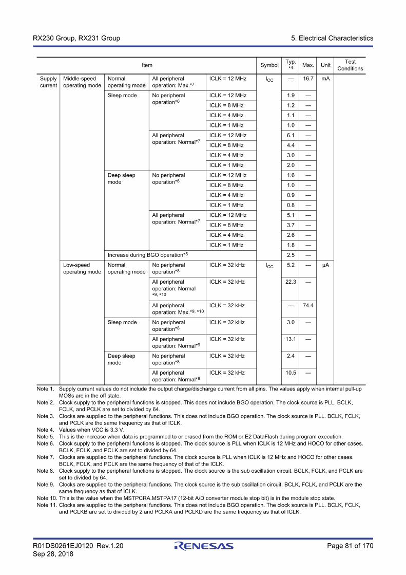
R01DS0261EJ0120 Rev.1.20 Page 81 of 170Sep 28, 2018
RX230 Group, RX231 Group 5. Electrical Characteristics
Note 1. Supply current values do not include the output charge/discharge current from all pins. The values apply when internal pull-up MOSs are in the off state.
Note 2. Clock supply to the peripheral functions is stopped. This does not include BGO operation. The clock source is PLL. BCLK, FCLK, and PCLK are set to divided by 64.
Note 3. Clocks are supplied to the peripheral functions. This does not include BGO operation. The clock source is PLL. BCLK, FCLK, and PCLK are the same frequency as that of ICLK.
Note 4. Values when VCC is 3.3 V.Note 5. This is the increase when data is programmed to or erased from the ROM or E2 DataFlash during program execution.Note 6. Clock supply to the peripheral functions is stopped. The clock source is PLL when ICLK is 12 MHz and HOCO for other cases.
BCLK, FCLK, and PCLK are set to divided by 64.Note 7. Clocks are supplied to the peripheral functions. The clock source is PLL when ICLK is 12 MHz and HOCO for other cases.
BCLK, FCLK, and PCLK are the same frequency of that of the ICLK.Note 8. Clock supply to the peripheral functions is stopped. The clock source is the sub oscillation circuit. BCLK, FCLK, and PCLK are
set to divided by 64.Note 9. Clocks are supplied to the peripheral functions. The clock source is the sub oscillation circuit. BCLK, FCLK, and PCLK are the
same frequency as that of ICLK.Note 10. This is the value when the MSTPCRA.MSTPA17 (12-bit A/D converter module stop bit) is in the module stop state.Note 11. Clocks are supplied to the peripheral functions. This does not include BGO operation. The clock source is PLL. BCLK, FCLK,
and PCLKB are set to divided by 2 and PCLKA and PCLKD are the same frequency as that of ICLK.
Supply current
Middle-speed operating mode
Normal operating mode
All peripheral operation: Max.*7
ICLK = 12 MHz ICC — 16.7 mA
Sleep mode No peripheral operation*6
ICLK = 12 MHz 1.9 —
ICLK = 8 MHz 1.2 —
ICLK = 4 MHz 1.1 —
ICLK = 1 MHz 1.0 —
All peripheral operation: Normal*7
ICLK = 12 MHz 6.1 —
ICLK = 8 MHz 4.4 —
ICLK = 4 MHz 3.0 —
ICLK = 1 MHz 2.0 —
Deep sleep mode
No peripheral operation*6
ICLK = 12 MHz 1.6 —
ICLK = 8 MHz 1.0 —
ICLK = 4 MHz 0.9 —
ICLK = 1 MHz 0.8 —
All peripheral operation: Normal*7
ICLK = 12 MHz 5.1 —
ICLK = 8 MHz 3.7 —
ICLK = 4 MHz 2.6 —
ICLK = 1 MHz 1.8 —
Increase during BGO operation*5 2.5 —
Low-speed operating mode
Normal operating mode
No peripheral operation*8
ICLK = 32 kHz ICC 5.2 — μA
All peripheral operation: Normal*9, *10
ICLK = 32 kHz 22.3 —
All peripheral operation: Max.*9, *10
ICLK = 32 kHz — 74.4
Sleep mode No peripheral operation*8
ICLK = 32 kHz 3.0 —
All peripheral operation: Normal*9
ICLK = 32 kHz 13.1 —
Deep sleep mode
No peripheral operation*8
ICLK = 32 kHz 2.4 —
All peripheral operation: Normal*9
ICLK = 32 kHz 10.5 —
Item Symbol Typ.*4 Max. Unit Test
Conditions

R01DS0261EJ0120 Rev.1.20 Page 82 of 170Sep 28, 2018
RX230 Group, RX231 Group 5. Electrical Characteristics
Figure 5.1 Voltage Dependency in High-Speed Operating Mode (Reference Data)
2.0 2.5 3.0 3.5 4.0 4.5 6.05.0 5.51.5
VCC (V)
Ta = 105°C, ICLK = 54MHz*2
Ta = 105°C, ICLK = 32MHz*2
Ta = 25°C, ICLK = 54MHz*1
Ta = 25°C, ICLK = 32MHz*1
Ta = 105°C, ICLK = 16MHz*2
Ta = 105°C, ICLK = 8MHz*2
Ta = 25°C, ICLK = 16MHz*1
Ta = 105°C, ICLK = 4MHz*2
Ta = 25°C, ICLK = 8MHz*1
Ta = 25°C, ICLK = 4MHz*1
50
40
30
20
10
0
ICC
(mA)
60
Ta = 105°C, ICLK = 54MHz*2Ta = 25°C, ICLK = 54MHz*1
Ta = 25°C, ICLK = 32MHz*1 Ta = 105°C, ICLK = 32MHz*2
Ta = 25°C, ICLK = 16MHz*1 Ta = 105°C, ICLK = 16MHz*2
Ta = 25°C, ICLK = 8MHz*1 Ta = 105°C, ICLK = 8MHz*2
Ta = 25°C, ICLK = 4MHz*1 Ta = 105°C, ICLK = 4MHz*2
Note 1. All peripheral operations except any BGO operation are operating normally. Indicates the average of the typical samples through actual measurement during product evaluation.
Note 2. All peripheral operations except any BGO operation are operating at maximum. Indicates the average of the upper-limit samples through actual measurement during product evaluation.
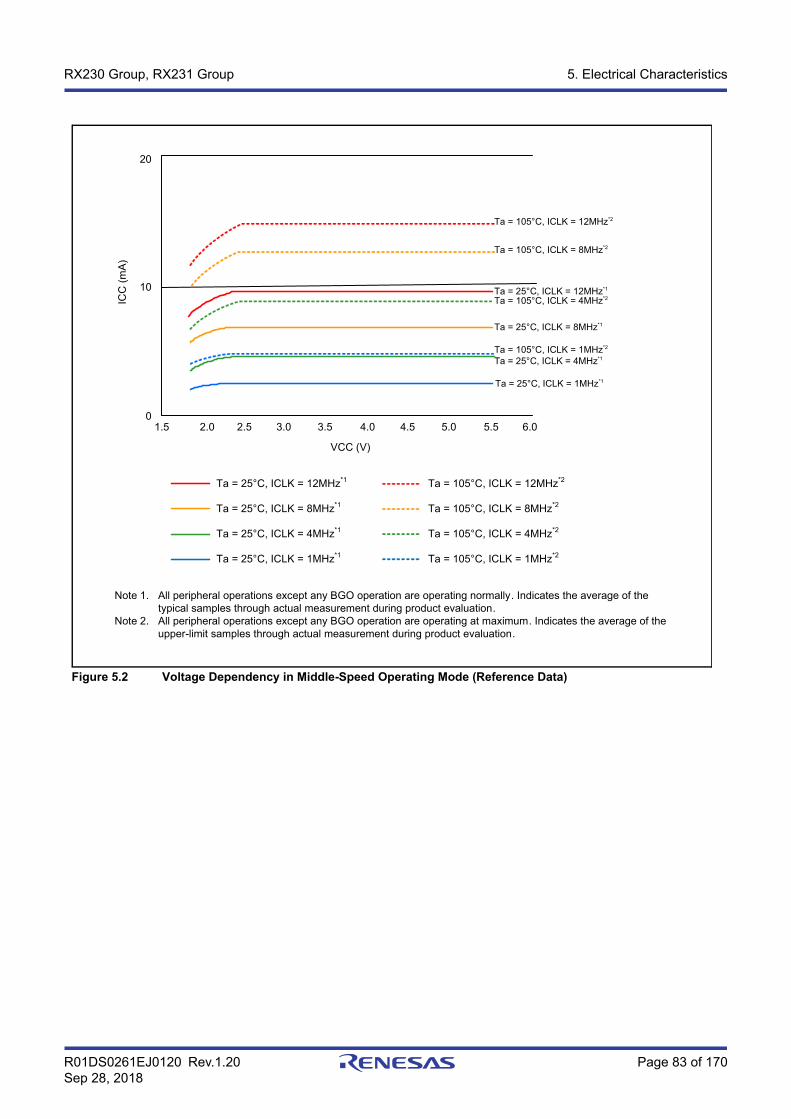
R01DS0261EJ0120 Rev.1.20 Page 83 of 170Sep 28, 2018
RX230 Group, RX231 Group 5. Electrical Characteristics
Figure 5.2 Voltage Dependency in Middle-Speed Operating Mode (Reference Data)
2.0 2.5 3.0 3.5 4.0 4.5 6.05.0 5.51.5
VCC (V)
Ta = 105°C, ICLK = 12MHz*2
Ta = 25°C, ICLK = 12MHz*1
Ta = 25°C, ICLK = 8MHz*1
Ta = 25°C, ICLK = 1MHz*1
Ta = 25°C, ICLK = 4MHz*1
20
10
0
ICC
(mA)
Ta = 105°C, ICLK = 8MHz*2
Ta = 105°C, ICLK = 4MHz*2
Ta = 105°C, ICLK = 1MHz*2
Ta = 105°C, ICLK = 12MHz*2Ta = 25°C, ICLK = 12MHz*1
Ta = 25°C, ICLK = 8MHz*1 Ta = 105°C, ICLK = 8MHz*2
Ta = 25°C, ICLK = 4MHz*1 Ta = 105°C, ICLK = 4MHz*2
Ta = 25°C, ICLK = 1MHz*1 Ta = 105°C, ICLK = 1MHz*2
Note 1. All peripheral operations except any BGO operation are operating normally. Indicates the average of the typical samples through actual measurement during product evaluation.
Note 2. All peripheral operations except any BGO operation are operating at maximum. Indicates the average of the upper-limit samples through actual measurement during product evaluation.
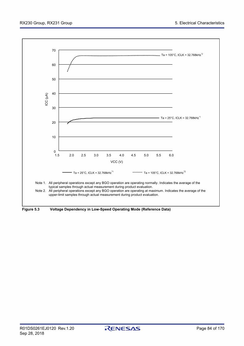
R01DS0261EJ0120 Rev.1.20 Page 84 of 170Sep 28, 2018
RX230 Group, RX231 Group 5. Electrical Characteristics
Figure 5.3 Voltage Dependency in Low-Speed Operating Mode (Reference Data)
2.0 2.5 3.0 3.5 4.0 4.5 6.05.0 5.51.5
50
40
30
20
10
0
ICC
(μA)
60
70
VCC (V)
Ta = 105°C, ICLK = 32.768kHz*2
Ta = 25°C, ICLK = 32.768kHz*1
Ta = 105°C, ICLK = 32.768kHz*2Ta = 25°C, ICLK = 32.768kHz*1
Note 1. All peripheral operations except any BGO operation are operating normally. Indicates the average of the typical samples through actual measurement during product evaluation.
Note 2. All peripheral operations except any BGO operation are operating at maximum. Indicates the average of the upper-limit samples through actual measurement during product evaluation.
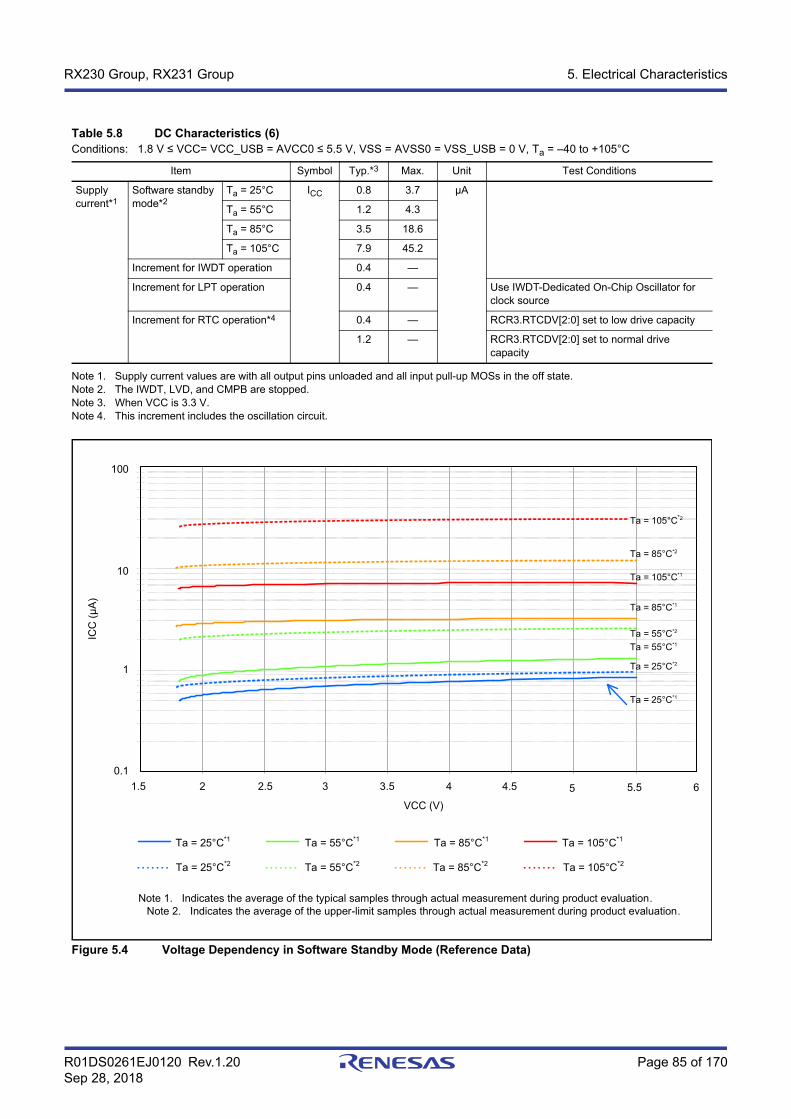
R01DS0261EJ0120 Rev.1.20 Page 85 of 170Sep 28, 2018
RX230 Group, RX231 Group 5. Electrical Characteristics
Note 1. Supply current values are with all output pins unloaded and all input pull-up MOSs in the off state.Note 2. The IWDT, LVD, and CMPB are stopped.Note 3. When VCC is 3.3 V.Note 4. This increment includes the oscillation circuit.
Figure 5.4 Voltage Dependency in Software Standby Mode (Reference Data)
Table 5.8 DC Characteristics (6)Conditions: 1.8 V ≤ VCC= VCC_USB = AVCC0 ≤ 5.5 V, VSS = AVSS0 = VSS_USB = 0 V, Ta = –40 to +105°C
Item Symbol Typ.*3 Max. Unit Test Conditions
Supply current*1
Software standby mode*2
Ta = 25°C ICC 0.8 3.7 μA
Ta = 55°C 1.2 4.3
Ta = 85°C 3.5 18.6
Ta = 105°C 7.9 45.2
Increment for IWDT operation 0.4 —
Increment for LPT operation 0.4 — Use IWDT-Dedicated On-Chip Oscillator for clock source
Increment for RTC operation*4 0.4 — RCR3.RTCDV[2:0] set to low drive capacity
1.2 — RCR3.RTCDV[2:0] set to normal drive capacity
Ta = 105°C*2
Ta = 105°C*1
Ta = 85°C*2
Ta = 85°C*1
Ta = 55°C*2
Ta = 25°C*2
Ta = 55°C*1
Ta = 25°C*1
Ta = 105°C*2
Ta = 105°C*1
Ta = 85°C*2
Ta = 85°C*1
Ta = 55°C*2
Ta = 55°C*1Ta = 25°C*1
Ta = 25°C*2
2 2.5 3 3.5 4 4.5 65 5.51.5
VCC (V)
10
ICC
(µA)
1
0.1
100
Note 1. Indicates the average of the typical samples through actual measurement during product evaluation.Note 2. Indicates the average of the upper-limit samples through actual measurement during product evaluation.
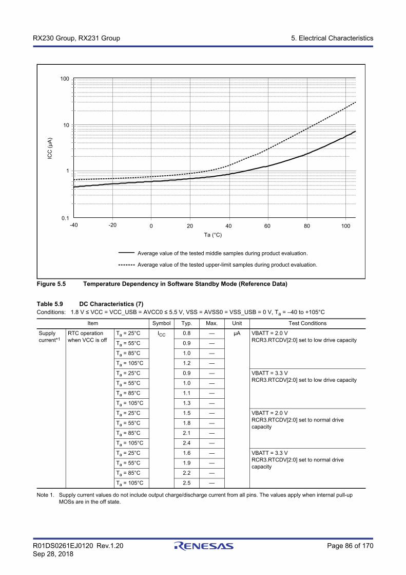
R01DS0261EJ0120 Rev.1.20 Page 86 of 170Sep 28, 2018
RX230 Group, RX231 Group 5. Electrical Characteristics
Figure 5.5 Temperature Dependency in Software Standby Mode (Reference Data)
Note 1. Supply current values do not include output charge/discharge current from all pins. The values apply when internal pull-up MOSs are in the off state.
Table 5.9 DC Characteristics (7)Conditions: 1.8 V ≤ VCC = VCC_USB = AVCC0 ≤ 5.5 V, VSS = AVSS0 = VSS_USB = 0 V, Ta = –40 to +105°C
Item Symbol Typ. Max. Unit Test Conditions
Supply current*1
RTC operation when VCC is off
Ta = 25°C ICC 0.8 — μA VBATT = 2.0 VRCR3.RTCDV[2:0] set to low drive capacityTa = 55°C 0.9 —
Ta = 85°C 1.0 —
Ta = 105°C 1.2 —
Ta = 25°C 0.9 — VBATT = 3.3 VRCR3.RTCDV[2:0] set to low drive capacityTa = 55°C 1.0 —
Ta = 85°C 1.1 —
Ta = 105°C 1.3 —
Ta = 25°C 1.5 — VBATT = 2.0 VRCR3.RTCDV[2:0] set to normal drive capacityTa = 55°C 1.8 —
Ta = 85°C 2.1 —
Ta = 105°C 2.4 —
Ta = 25°C 1.6 — VBATT = 3.3 VRCR3.RTCDV[2:0] set to normal drive capacityTa = 55°C 1.9 —
Ta = 85°C 2.2 —
Ta = 105°C 2.5 —
-40 -20 0 20 40 60 80 1000.1
1
10
100
ICC
(µA)
Ta (°C)
Average value of the tested upper-limit samples during product evaluation.
Average value of the tested middle samples during product evaluation.
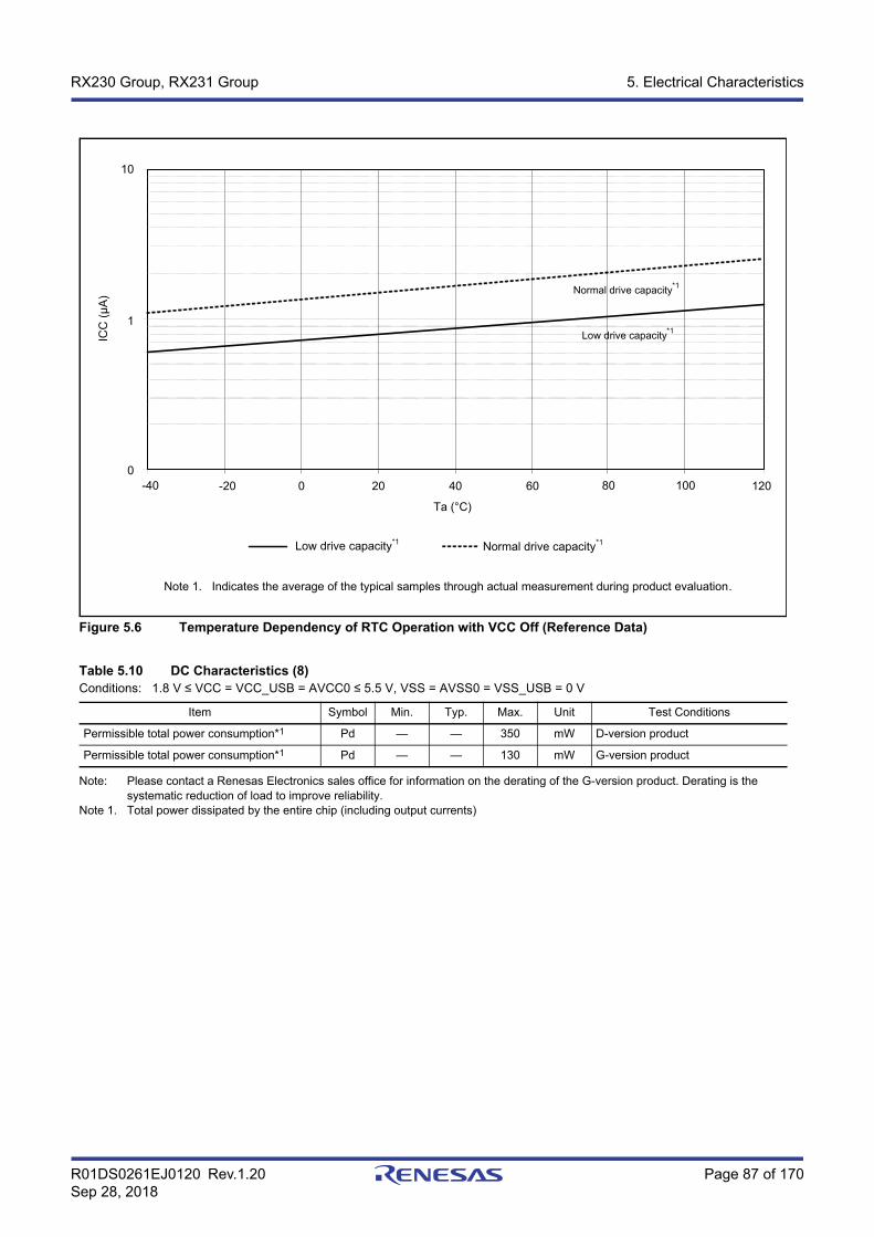
R01DS0261EJ0120 Rev.1.20 Page 87 of 170Sep 28, 2018
RX230 Group, RX231 Group 5. Electrical Characteristics
Figure 5.6 Temperature Dependency of RTC Operation with VCC Off (Reference Data)
Note: Please contact a Renesas Electronics sales office for information on the derating of the G-version product. Derating is the systematic reduction of load to improve reliability.
Note 1. Total power dissipated by the entire chip (including output currents)
Table 5.10 DC Characteristics (8)Conditions: 1.8 V ≤ VCC = VCC_USB = AVCC0 ≤ 5.5 V, VSS = AVSS0 = VSS_USB = 0 V
Item Symbol Min. Typ. Max. Unit Test Conditions
Permissible total power consumption*1 Pd — — 350 mW D-version product
Permissible total power consumption*1 Pd — — 130 mW G-version product
10
1
0
ICC
(µA)
-40 -20 0 20 40 60 80 100 120
Ta (°C)
Low drive capacity*1 Normal drive capacity*1
Low drive capacity*1
Normal drive capacity*1
Note 1. Indicates the average of the typical samples through actual measurement during product evaluation.
R01DS0261EJ0120 Rev.1.20 Page 88 of 170Sep 28, 2018
RX230 Group, RX231 Group 5. Electrical Characteristics
Note 1. The value of the D/A converter is the value of the power supply current including the reference current.Note 2. Current consumed only by the USB module.Note 3. Includes the current supplied from the pull-up resistor of the USB0_DP pin to the pull-down resistor of the host device, in
addition to the current consumed by this MCU during the suspended state.Note 4. Current consumed by the power supplies (VCC and VCC_USB).Note 5. Current consumed only by the comparator B module.Note 6. Current consumed by the power supply (VCC).Note 7. When VCC = AVCC0 = VCC_USB = 3.3 V.
Table 5.11 DC Characteristics (9)Conditions: 1.8 V ≤ VCC = VCC_USB = AVCC0 ≤ 5.5 V, VSS = AVSS0 = VSS_USB = 0 V, Ta = –40 to +105°C
Item Symbol Min. Typ.*7 Max. Unit Test Conditions
Analog power supply current
During A/D conversion (at high-speed conversion) IAVCC — 0.7 1.7 mA
During A/D conversion (in low-current mode) — 0.6 1.0
During D/A conversion (per channel)*1 — 0.4 0.8
Waiting for A/D and D/A conversion (all units) — — 0.4 μA
Reference power supply current
During A/D conversion (at high-speed conversion) IREFH0 — 25 150 μA
Waiting for A/D conversion (all units) — — 60 nA
During D/A conversion (per channel) IREFH — 50 100 μA
Waiting for D/A conversion (all units) — — 100 nA
LVD1, 2 per channel ILVD — 0.15 — μA
Temperature sensor*6
— ITEMP — 75 — μA
Comparator B operating current*6
Window mode ICMP*5 — 12.5 28.6 μA
Comparator high-speed mode (per channel) — 3.2 16.2 μA
Comparator low-speed mode (per channel) — 1.7 4.4 μA
CTSU operating current
When sleep mode Base clock frequency: 2MHz Pin capacitance: 50pF
ICTSU — 150 — μA
USB operating current*4
During USB communication operation under the following settings and conditions
• Host controller operation is set to full-speed modeBulk OUT transfer (64 bytes) × 1,bulk IN transfer (64 bytes) × 1
• Connect peripheral devices via a 1-meter USB cable from the USB port.
IUSBH*2 — 4.3(VCC)
0.9(VCC_USB)
— mA
During USB communication operation under the following settings and conditions
• Function controller operation is set to full-speed modeBulk OUT transfer (64 bytes) × 1,bulk IN transfer (64 bytes) × 1
• Connect the host device via a 1-meter USB cable from the USB port.
IUSBF*2 — 3.6(VCC)
1.1(VCC_USB)
— mA
During suspended state under the following setting and conditions
• Function controller operation is set to full-speed mode (pull up the USB0_DP pin)
• Software standby mode• Connect the host device via a 1-meter USB
cable from the USB port.
ISUSP*3 — 0.35(VCC)170
(VCC_USB)
— μA
Table 5.12 DC Characteristics (10)Conditions: 1.8 V ≤ VCC = VCC_USB = AVCC0 ≤ 5.5 V, VSS = AVSS0 = VSS_USB = 0 V, Ta = –40 to +105°C
Item Symbol Min. Typ. Max. Unit Test Conditions
RAM standby voltage VRAM 1.8 — — V

R01DS0261EJ0120 Rev.1.20 Page 89 of 170Sep 28, 2018
RX230 Group, RX231 Group 5. Electrical Characteristics
Note 1. When OFS1.(FASTSTUP, LVDAS) bits are 11b.Note 2. When OFS1.(FASTSTUP, LVDAS) bits are 01b.Note 3. When OFS1.LVDAS bit is 0.Note 4. Turn on the power supply voltage according to the normal startup rising gradient because the settings in the OFS1 register are
not read in boot mode.
Figure 5.7 Ripple Waveform
Note: The recommended capacitance is 4.7 μF. Variations in connected capacitors should be within the above range.
Table 5.13 DC Characteristics (11)Conditions: 0 V ≤ VCC = VCC_USB = AVCC0 ≤ 5.5 V, VSS = AVSS0 = VSS_USB = 0 V, Ta = –40 to +105°C
Item Symbol Min. Typ. Max. Unit Test Conditions
Power-on VCC rising gradient
At normal startup*1 SrVCC 0.02 — 20 ms/V
During fast startup time*2 0.02 — 2
Voltage monitoring 0 reset enabled at startup*3, *4
0.02 — —
Table 5.14 DC Characteristics (12)Conditions: 1.8 V ≤ VCC = VCC_USB = AVCC0 ≤ 5.5 V, VSS = AVSS0 = VSS_USB = 0 V, Ta = –40 to +105°CThe ripple voltage must meet the allowable ripple frequency fr (VCC) within the range between the VCC upper limit and lower limit. When VCC change exceeds VCC ±10%, the allowable voltage change rising/falling gradient dt/dVCC must be met.
Item Symbol Min. Typ. Max. Unit Test Conditions
Allowable ripple frequency fr (VCC) — — 10 kHz Figure 5.7Vr (VCC) ≤ VCC × 0.2
— — 1 MHz Figure 5.7Vr (VCC) ≤ VCC × 0.08
— — 10 MHz Figure 5.7Vr (VCC) ≤ VCC × 0.06
Allowable voltage change rising/falling gradient
dt/dVCC 1.0 — — ms/V When VCC change exceeds VCC ±10%
Table 5.15 DC Characteristics (13)Conditions: 1.8 V ≤ VCC = VCC_USB = AVCC0 ≤ 5.5 V, VSS = AVSS0 = VSS_USB = 0 V, Ta = –40 to +105°C
Item Symbol Min. Typ. Max. Unit Test Conditions
Permissible error of VCL pin external capacitance
CVCL 1.4 4.7 7.0 μF
Vr (VCC)VCC
1 / fr (VCC)

R01DS0261EJ0120 Rev.1.20 Page 90 of 170Sep 28, 2018
RX230 Group, RX231 Group 5. Electrical Characteristics
Note: Do not exceed the permissible total supply current.
Table 5.16 Permissible Output Currents (1)Conditions: 1.8 V ≤ VCC = VCC_USB = AVCC0 ≤ 5.5 V, VSS = AVSS0 = VSS_USB = 0 V, Ta = –40 to +85°C
Item Symbol Max. Unit
Permissible output low current(average value per pin)
Ports 40 to 47, ports 03, 05, 07, port 36, 37 IOL 4.0 mA
Ports other than above Normal output mode 4.0
High-drive output mode 8.0
Permissible output low current(maximum value per pin)
Ports 40 to 47, ports 03, 05, 07, ports 36, 37 4.0
Ports other than above Normal output mode 4.0
High-drive output mode 8.0
Permissible output low current Total of ports 40 to 47, ports 03, 05, 07 ΣIOL 40
Total of ports 12 to 17, ports 20 to 27, ports 30 to 37, port PJ3 40
Total of ports 50 to 55, ports C0 to C7, ports B0 to B7 40
Total of ports E0 to E7, ports A0 to A7, ports D0 to D4 40
Total of all output pins 80
Permissible output high current(average value per pin)
Ports 40 to 47, ports 03, 05, 07, ports 36, 37 IOH –4.0
Ports other than above Normal output mode –4.0
High-drive output mode –8.0
Permissible output high current(maximum value per pin)
Ports 40 to 47, ports 03, 05, 07, ports 36, 37 –4.0
Ports other than above Normal output mode –4.0
High-drive output mode –8.0
Permissible output high current Total of ports 40 to 47, ports 03, 05, 07 ΣIOH –40
Total of ports 12 to 17, ports 20 to 27, ports 30 to 37, port PJ3 –40
Total of ports 50 to 55, ports C0 to C7, ports B0 to B7 –40
Total of ports E0 to E7, ports A0 to A7, ports D0 to D4 –40
Total of all output pins –80
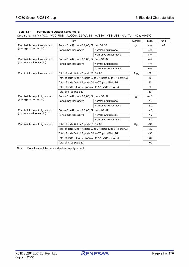
R01DS0261EJ0120 Rev.1.20 Page 91 of 170Sep 28, 2018
RX230 Group, RX231 Group 5. Electrical Characteristics
Note: Do not exceed the permissible total supply current.
Table 5.17 Permissible Output Currents (2)Conditions: 1.8 V ≤ VCC = VCC_USB = AVCC0 ≤ 5.5 V, VSS = AVSS0 = VSS_USB = 0 V, Ta = –40 to +105°C
Item Symbol Max. Unit
Permissible output low current(average value per pin)
Ports 40 to 47, ports 03, 05, 07, port 36, 37 IOL 4.0 mA
Ports other than above Normal output mode 4.0
High-drive output mode 8.0
Permissible output low current(maximum value per pin)
Ports 40 to 47, ports 03, 05, 07, ports 36, 37 4.0
Ports other than above Normal output mode 4.0
High-drive output mode 8.0
Permissible output low current Total of ports 40 to 47, ports 03, 05, 07 ΣIOL 30
Total of ports 12 to 17, ports 20 to 27, ports 30 to 37, port PJ3 30
Total of ports 50 to 55, ports C0 to C7, ports B0 to B7 30
Total of ports E0 to E7, ports A0 to A7, ports D0 to D4 30
Total of all output pins 60
Permissible output high current(average value per pin)
Ports 40 to 47, ports 03, 05, 07, ports 36, 37 IOH –4.0
Ports other than above Normal output mode –4.0
High-drive output mode –8.0
Permissible output high current(maximum value per pin)
Ports 40 to 47, ports 03, 05, 07, ports 36, 37 –4.0
Ports other than above Normal output mode –4.0
High-drive output mode –8.0
Permissible output high current Total of ports 40 to 47, ports 03, 05, 07 ΣIOH –30
Total of ports 12 to 17, ports 20 to 27, ports 30 to 37, port PJ3 –30
Total of ports 50 to 55, ports C0 to C7, ports B0 to B7 –30
Total of ports E0 to E7, ports A0 to A7, ports D0 to D4 –30
Total of all output pins –60

R01DS0261EJ0120 Rev.1.20 Page 92 of 170Sep 28, 2018
RX230 Group, RX231 Group 5. Electrical Characteristics
Table 5.18 Output Values of Voltage (1)Conditions: 1.8 V ≤ VCC = VCC_USB = AVCC0 < 2.7 V, VSS = AVSS0 = VSS_USB = 0 V, Ta = –40 to +105°C
Item Symbol Min. Max. Unit Test Conditions
Output low All output ports Normal output mode VOL — 0.3 V IOL = 0.5 mA
High-drive output mode — 0.3 IOL = 1.0 mA
Output high All output ports Normal output mode
Ports 03, 05, 07, Ports 40 to 47
VOH AVCC0 – 0.3 — V IOH = –0.5 mA
Ports other than above
VCC – 0.3 —
High-drive output mode VCC – 0.3 — IOH = –1.0 mA
Table 5.19 Output Values of Voltage (2)Conditions: 2.7 V ≤ VCC = VCC_USB = AVCC0 < 4.0 V, VSS = AVSS0 = VSS_USB = 0 V, Ta = –40 to +105°C
Item Symbol Min. Max. Unit Test Conditions
Output low All output ports (except for RIIC)
Normal output mode VOL — 0.5 V IOL = 1.0 mA
High-drive output mode — 0.5 IOL = 2.0 mA
RIIC pins Standard mode (Normal output mode)
— 0.4 IOL = 3.0 mA
Fast mode (High-drive output mode)
— 0.6 IOL = 6.0 mA
Output high All output ports Normal output mode
Ports 03, 05, 07, Ports 40 to 47
VOH AVCC0 – 0.5 — V IOH = –1.0 mA
Ports other than above
VCC – 0.5
High-drive output mode VCC – 0.5 — IOH = –2.0 mA
Table 5.20 Output Values of Voltage (3)Conditions: 4.0 V ≤ VCC = VCC_USB = AVCC0 ≤ 5.5 V, VSS = AVSS0 = VSS_USB = 0 V, Ta = –40 to +105°C
Item Symbol Min. Max. Unit Test Conditions
Output low All output ports (except for RIIC)
Normal output mode VOL — 0.8 V IOL = 2.0 mA
High-drive output mode — 0.8 IOL = 4.0 mA
RIIC pins Standard mode(Normal output mode)
— 0.4 IOL = 3.0 mA
Fast mode (High-drive output mode)
— 0.6 IOL = 6.0 mA
Output high All output ports Normal output mode
Ports 03, 05, 07, Ports 40 to 47
VOH AVCC0 – 0.8 — V IOH = –2.0 mA
Ports other than above
VCC – 0.8 —
High-drive output mode VCC – 0.8 — IOH = –4.0 mA
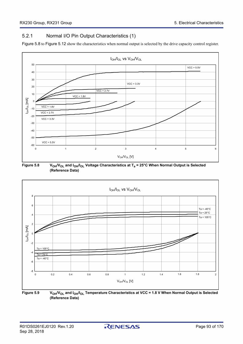
R01DS0261EJ0120 Rev.1.20 Page 93 of 170Sep 28, 2018
RX230 Group, RX231 Group 5. Electrical Characteristics
5.2.1 Normal I/O Pin Output Characteristics (1)Figure 5.8 to Figure 5.12 show the characteristics when normal output is selected by the drive capacity control register.
Figure 5.8 VOH/VOL and IOH/IOL Voltage Characteristics at Ta = 25°C When Normal Output is Selected (Reference Data)
Figure 5.9 VOH/VOL and IOH/IOL Temperature Characteristics at VCC = 1.8 V When Normal Output is Selected (Reference Data)
IOH/IOL vs VOH/VOL
I OH/I O
L [m
A]
VCC = 5.5V
VCC = 3.3V
VCC = 2.7V
VCC = 1.8V
VCC = 1.8V
VCC = 2.7V
VCC = 3.3V
0 1 2 3 4 5 6
VCC = 5.5V
50
40
30
20
10
0
-10
-20
-30
-40
-50
-60
VOH/VOL [V]
VOH/VOL [V]
0 0.2 0.4 0.6 0.8 1 1.2 1.4 1.6 1.8 2
I OH/I O
L [m
A]
0
2
4
6
8
-2
-4
-6
-8
Ta = 105°C
Ta = 25°CTa = -40°C
Ta = 105°C
Ta = 25°CTa = -40°C
IOH/IOL vs VOH/VOL
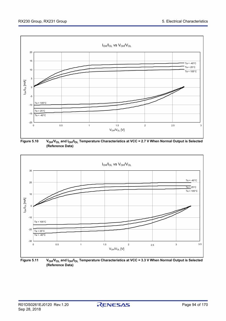
R01DS0261EJ0120 Rev.1.20 Page 94 of 170Sep 28, 2018
RX230 Group, RX231 Group 5. Electrical Characteristics
Figure 5.10 VOH/VOL and IOH/IOL Temperature Characteristics at VCC = 2.7 V When Normal Output is Selected (Reference Data)
Figure 5.11 VOH/VOL and IOH/IOL Temperature Characteristics at VCC = 3.3 V When Normal Output is Selected (Reference Data)
VOH/VOL [V]0 0.5 1.51 2.5 3
I OH/I O
L [m
A]
0
5
10
15
20
-5
-10
-15
-20
Ta = 105°C
Ta = 25°C
Ta = -40°C
Ta = 105°C
Ta = 25°CTa = -40°C
IOH/IOL vs VOH/VOL
2
VOH/VOL [V]0 0.5 1.51 2.5 3
I OH/I O
L [m
A]
0
10
20
-10
-20
Ta = 105°C
Ta = 25°C
Ta = -40°C
Ta = 105°CTa = 25°C
Ta = -40°C
IOH/IOL vs VOH/VOL
2 3.5
30
-30
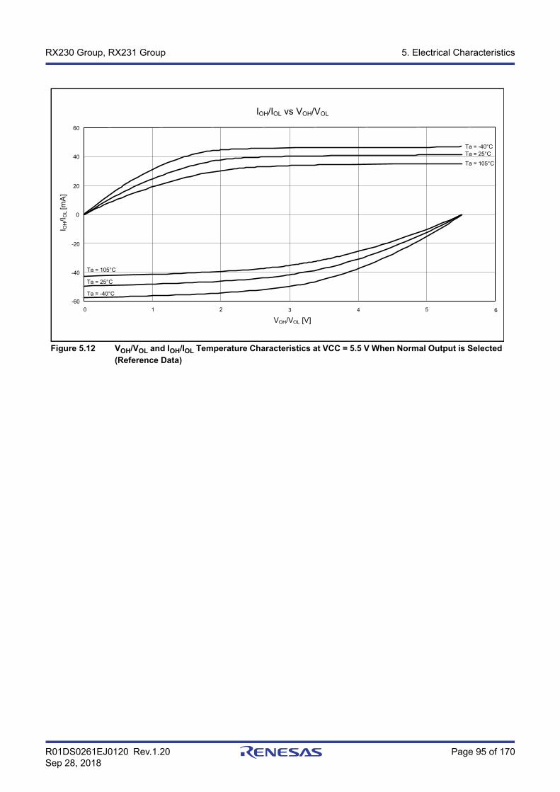
R01DS0261EJ0120 Rev.1.20 Page 95 of 170Sep 28, 2018
RX230 Group, RX231 Group 5. Electrical Characteristics
Figure 5.12 VOH/VOL and IOH/IOL Temperature Characteristics at VCC = 5.5 V When Normal Output is Selected (Reference Data)
VOH/VOL [V]0 21 4 5
I OH/I O
L [m
A]
0
20
40
-20
-40 Ta = 105°C
Ta = 25°C
Ta = -40°C
Ta = 105°CTa = 25°CTa = -40°C
IOH/IOL vs VOH/VOL
3 6
60
-60

R01DS0261EJ0120 Rev.1.20 Page 96 of 170Sep 28, 2018
RX230 Group, RX231 Group 5. Electrical Characteristics
5.2.2 Normal I/O Pin Output Characteristics (2)Figure 5.13 to Figure 5.17 show the characteristics when high-drive output is selected by the drive capacity control register.
Figure 5.13 VOH/VOL and IOH/IOL Voltage Characteristics at Ta = 25°C When High-Drive Output is Selected (Reference Data)
Figure 5.14 VOH/VOL and IOH/IOL Temperature Characteristics at VCC = 1.8 V When High-Drive Output is Selected (Reference Data)
0 1 2 3 4 5 6-150
-100
-50
0
50
100
150IOH/IOL vs VOH/VOL
VOH/VOL [V]
I OH/I O
L [m
A]
VCC=3.3V
VCC=3.3V
VCC=2.7V
VCC=2.7V
VCC=1.8V
VCC=1.8V
VCC=5.5V
VCC=5.5V
VOH/VOL [V]0 0.2 0.4 0.6 0.8 1 1.2 1.4 1.6 1.8 2
I OH/I O
L [m
A]
0
4
8
12
16
-4
-8
-12
-16
Ta = 105°C
Ta = 25°C
Ta = -40°C
Ta = 105°CTa = 25°CTa = -40°C
IOH/IOL vs VOH/VOL
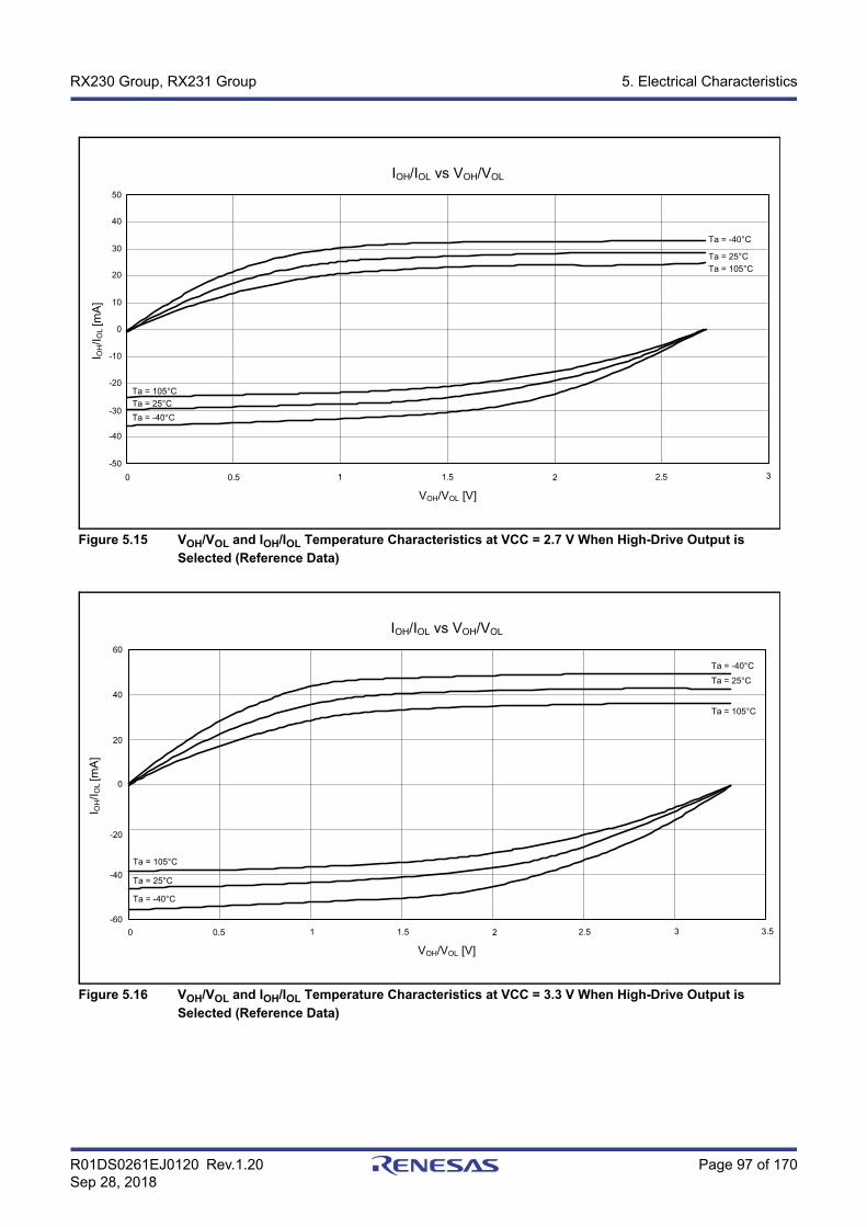
R01DS0261EJ0120 Rev.1.20 Page 97 of 170Sep 28, 2018
RX230 Group, RX231 Group 5. Electrical Characteristics
Figure 5.15 VOH/VOL and IOH/IOL Temperature Characteristics at VCC = 2.7 V When High-Drive Output is Selected (Reference Data)
Figure 5.16 VOH/VOL and IOH/IOL Temperature Characteristics at VCC = 3.3 V When High-Drive Output is Selected (Reference Data)
VOH/VOL [V]0 0.5 1 1.5 2 2.5 3
I OH/I O
L [m
A]
0
10
20
30
40
-20
-30
-40
-50
Ta = 105°CTa = 25°CTa = -40°C
Ta = 105°CTa = 25°C
Ta = -40°C
IOH/IOL vs VOH/VOL
-10
50
VOH/VOL [V]0 0.5 1 1.5 2 2.5 3
I OH/I O
L [m
A]
0
20
40
-20
-40
-60
Ta = 105°C
Ta = 25°C
Ta = -40°C
Ta = 105°C
Ta = 25°CTa = -40°C
IOH/IOL vs VOH/VOL
60
3.5
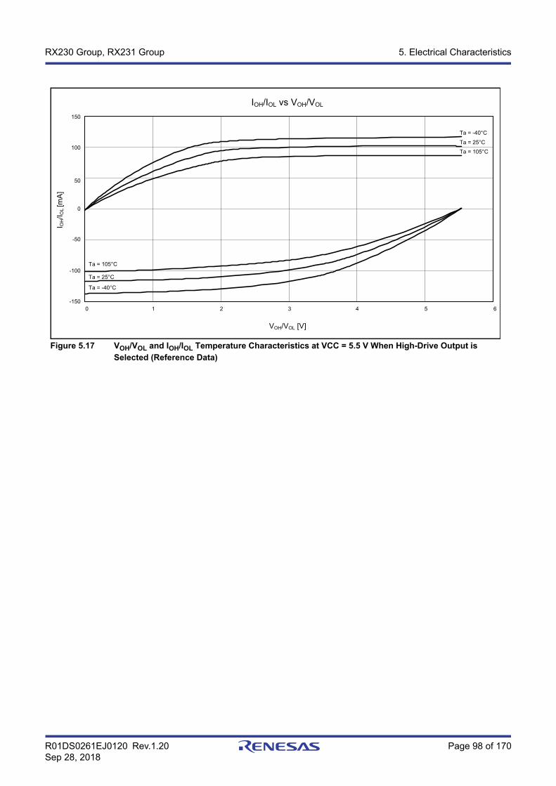
R01DS0261EJ0120 Rev.1.20 Page 98 of 170Sep 28, 2018
RX230 Group, RX231 Group 5. Electrical Characteristics
Figure 5.17 VOH/VOL and IOH/IOL Temperature Characteristics at VCC = 5.5 V When High-Drive Output is Selected (Reference Data)
VOH/VOL [V]
0 41 52 3
I OH/I O
L [m
A]
0
50
100
-50
-150
Ta = 105°C
Ta = 25°C
Ta = -40°C
Ta = 105°CTa = 25°CTa = -40°C
IOH/IOL vs VOH/VOL
150
6
-100
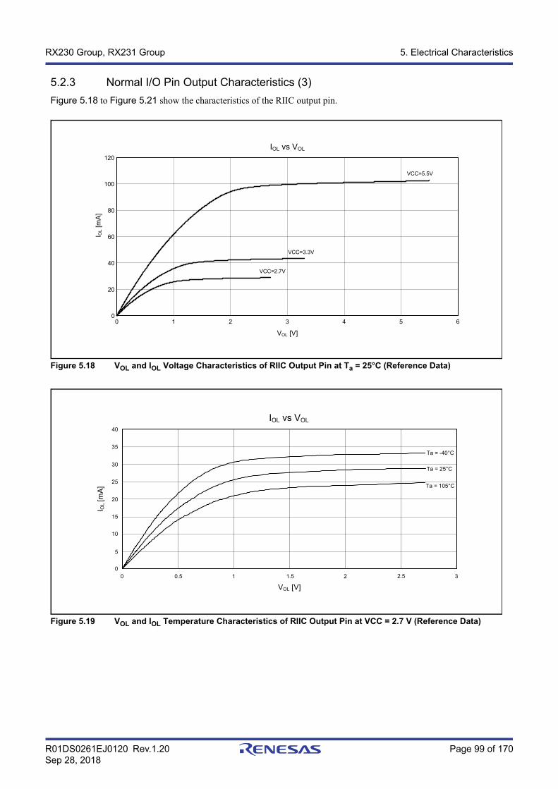
R01DS0261EJ0120 Rev.1.20 Page 99 of 170Sep 28, 2018
RX230 Group, RX231 Group 5. Electrical Characteristics
5.2.3 Normal I/O Pin Output Characteristics (3)Figure 5.18 to Figure 5.21 show the characteristics of the RIIC output pin.
Figure 5.18 VOL and IOL Voltage Characteristics of RIIC Output Pin at Ta = 25°C (Reference Data)
Figure 5.19 VOL and IOL Temperature Characteristics of RIIC Output Pin at VCC = 2.7 V (Reference Data)
0 1 2 3 4 5 60
20
40
60
80
100
120IOL vs VOL
VOL [V]
I OL [
mA]
VCC=3.3V
VCC=2.7V
VCC=5.5V
I OL [m
A]
Ta = 25°C
Ta = 105°C
Ta = -40°C
IOL vs VOL
0
5
10
15
20
25
30
35
40
VOL [V]0 0.5 1 1.5 2 2.5 3

R01DS0261EJ0120 Rev.1.20 Page 100 of 170Sep 28, 2018
RX230 Group, RX231 Group 5. Electrical Characteristics
Figure 5.20 VOL and IOL Temperature Characteristics of RIIC Output Pin at VCC = 3.3 V (Reference Data)
Figure 5.21 VOL and IOL Temperature Characteristics of RIIC Output Pin at VCC = 5.5 V (Reference Data)
IOL vs VOL
I OL [
mA]
VOL [V]
10
20
30
50
40
00 0.5 1 1.5 2 2.5 3 3.5
Ta = 25°C
Ta = 105°C
Ta = -40°C
60
Ta = 105°C
I OL [
mA]
20
40
80
60
00 1 2 3 4 5 6
100
120
140IOL vs VOL
VOL [V]
Ta = -40°C
Ta = 25°C
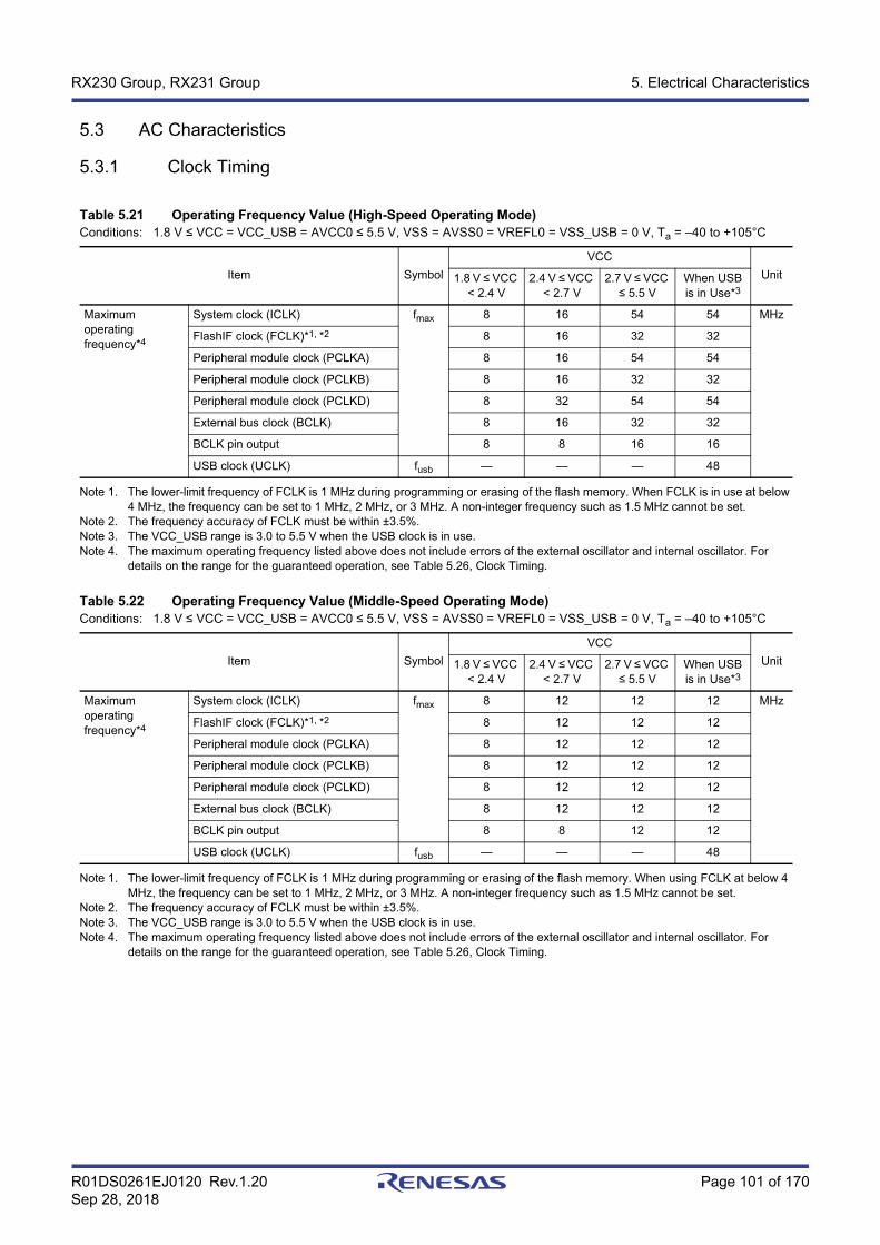
R01DS0261EJ0120 Rev.1.20 Page 101 of 170Sep 28, 2018
RX230 Group, RX231 Group 5. Electrical Characteristics
5.3 AC Characteristics
5.3.1 Clock Timing
Note 1. The lower-limit frequency of FCLK is 1 MHz during programming or erasing of the flash memory. When FCLK is in use at below 4 MHz, the frequency can be set to 1 MHz, 2 MHz, or 3 MHz. A non-integer frequency such as 1.5 MHz cannot be set.
Note 2. The frequency accuracy of FCLK must be within ±3.5%.Note 3. The VCC_USB range is 3.0 to 5.5 V when the USB clock is in use.Note 4. The maximum operating frequency listed above does not include errors of the external oscillator and internal oscillator. For
details on the range for the guaranteed operation, see Table 5.26, Clock Timing.
Note 1. The lower-limit frequency of FCLK is 1 MHz during programming or erasing of the flash memory. When using FCLK at below 4 MHz, the frequency can be set to 1 MHz, 2 MHz, or 3 MHz. A non-integer frequency such as 1.5 MHz cannot be set.
Note 2. The frequency accuracy of FCLK must be within ±3.5%.Note 3. The VCC_USB range is 3.0 to 5.5 V when the USB clock is in use.Note 4. The maximum operating frequency listed above does not include errors of the external oscillator and internal oscillator. For
details on the range for the guaranteed operation, see Table 5.26, Clock Timing.
Table 5.21 Operating Frequency Value (High-Speed Operating Mode)Conditions: 1.8 V ≤ VCC = VCC_USB = AVCC0 ≤ 5.5 V, VSS = AVSS0 = VREFL0 = VSS_USB = 0 V, Ta = –40 to +105°C
Item SymbolVCC
Unit1.8 V ≤ VCC < 2.4 V
2.4 V ≤ VCC < 2.7 V
2.7 V ≤ VCC ≤ 5.5 V
When USBis in Use*3
Maximum operating frequency*4
System clock (ICLK) fmax 8 16 54 54 MHz
FlashIF clock (FCLK)*1, *2 8 16 32 32
Peripheral module clock (PCLKA) 8 16 54 54
Peripheral module clock (PCLKB) 8 16 32 32
Peripheral module clock (PCLKD) 8 32 54 54
External bus clock (BCLK) 8 16 32 32
BCLK pin output 8 8 16 16
USB clock (UCLK) fusb — — — 48
Table 5.22 Operating Frequency Value (Middle-Speed Operating Mode)Conditions: 1.8 V ≤ VCC = VCC_USB = AVCC0 ≤ 5.5 V, VSS = AVSS0 = VREFL0 = VSS_USB = 0 V, Ta = –40 to +105°C
Item SymbolVCC
Unit1.8 V ≤ VCC < 2.4 V
2.4 V ≤ VCC < 2.7 V
2.7 V ≤ VCC ≤ 5.5 V
When USBis in Use*3
Maximum operating frequency*4
System clock (ICLK) fmax 8 12 12 12 MHz
FlashIF clock (FCLK)*1, *2 8 12 12 12
Peripheral module clock (PCLKA) 8 12 12 12
Peripheral module clock (PCLKB) 8 12 12 12
Peripheral module clock (PCLKD) 8 12 12 12
External bus clock (BCLK) 8 12 12 12
BCLK pin output 8 8 12 12
USB clock (UCLK) fusb — — — 48

R01DS0261EJ0120 Rev.1.20 Page 102 of 170Sep 28, 2018
RX230 Group, RX231 Group 5. Electrical Characteristics
Note 1. Programming and erasing the flash memory is impossible.Note 2. The A/D converter cannot be used.Note 3. The maximum operating frequency listed above does not include errors of the external oscillator. For details on the range for the
guaranteed operation, see Table 5.26, Clock Timing.
Table 5.23 Operating Frequency Value (Low-Speed Operating Mode)Conditions: 1.8 V ≤ VCC = VCC_USB = AVCC0 ≤ 5.5 V, VSS = AVSS0 = VREFL0 = VSS_USB = 0 V, Ta = –40 to +105°C
Item SymbolVCC
Unit1.8 V ≤ VCC < 2.4 V
2.4 V ≤ VCC < 2.7 V
2.7 V ≤ VCC ≤ 5.5 V
Maximum operating frequency*3
System clock (ICLK) fmax 32.768 kHz
FlashIF clock (FCLK)*1 32.768
Peripheral module clock (PCLKA) 32.768
Peripheral module clock (PCLKB) 32.768
Peripheral module clock (PCLKD)*2 32.768
External bus clock (BCLK) 32.768
BCLK pin output 32.768
Table 5.24 BCLK Clock Timing (1)Conditions: 2.7 V ≤ VCC= VCC_USB = AVCC0 ≤ 5.5 V, VSS = AVSS0 = VREFL0 = VSS_USB = 0 V,
fBCLK ≤ 32 MHz (BCLK pin output frequency ≤ 16 MHz), Ta = –40 to +105°C
Item Symbol Min. Typ. Max. Unit Test Conditions
BCLK pin output cycle time tBcyc 62.5 — — ns Figure 5.22
BCLK pin output high pulse width tCH 15 — — ns
BCLK pin output low pulse width tCL 15 — — ns
BCLK pin output rise time tCr — — 12 ns
BCLK pin output fall time tCf — — 12 ns
Table 5.25 BCLK Clock Timing (2)Conditions: 1.8 V ≤ VCC = VCC_USB = AVCC0 < 2.7 V, VSS = AVSS0 = VREFL0 = VSS_USB = 0 V,
fBCLK ≤ 16 MHz (BCLK pin output frequency ≤ 8 MHz), Ta = –40 to +105°C
Item Symbol Min. Typ. Max. Unit Test Conditions
BCLK pin output cycle time tBcyc 125 — — ns Figure 5.22
BCLK pin output high pulse width tCH 30 — — ns
BCLK pin output low pulse width tCL 30 — — ns
BCLK pin output rise time tCr — — 25 ns
BCLK pin output fall time tCf — — 25 ns

R01DS0261EJ0120 Rev.1.20 Page 103 of 170Sep 28, 2018
RX230 Group, RX231 Group 5. Electrical Characteristics
Note 1. Time until the clock can be used after the main clock oscillator stop bit (MOSCCR.MOSTP) is set to 0 (operating).Note 2. Reference values when an 8-MHz resonator is used.
When specifying the main clock oscillator stabilization time, set the MOSCWTCR register with a stabilization time value that is equal to or greater than the resonator-manufacturer-recommended value.After the MOSCCR.MOSTP bit is changed to enable the main clock oscillator, confirm that the OSCOVFSR.MOOVF flag has become 1, and then start using the main clock.
Note 3. The VCC range should be 2.4 to 5.5 V when the PLL is used.Note 4. Reference values when a 32.768-kHz resonator is used.
After the setting of the SOSCCR.SOSTP bit or RCR3.RTCEN bit is changed to operate the sub-clock oscillator, only start using the sub-clock after the sub-clock oscillation stabilization wait time that is equal to or greater than the oscillator-manufacturer-recommended value has elapsed.
Note 5. The VCC range should be 3.0 to 5.5 V when the USBPLL is used.Note 6. The input frequency can be set to 6 or 8 MHz and the oscillation frequency can be set to 48 MHz only.Note 7. Only 32.768 kHz can be used.
Table 5.26 Clock TimingConditions: 1.8 V ≤ VCC = VCC_USB = AVCC0 ≤ 5.5 V, VSS = AVSS0 = VREFL0 = VSS_USB = 0 V, Ta = –40 to +105°C
Item Symbol Min. Typ. Max. Unit Test Conditions
EXTAL external clock input cycle time tXcyc 50 — — ns Figure 5.23
EXTAL external clock input high pulse width tXH 20 — — ns
EXTAL external clock input low pulse width tXL 20 — — ns
EXTAL external clock rise time tXr — — 5 ns
EXTAL external clock fall time tXf — — 5 ns
EXTAL external clock input wait time*1 tXWT 0.5 — — μs
Main clock oscillator oscillation frequency*2
2.4 ≤ VCC ≤ 5.5 fMAIN 1 — 20 MHz
1.8 ≤ VCC < 2.4 1 — 8
Main clock oscillation stabilization time (crystal)*2 tMAINOSC — 3 — ms Figure 5.24
Main clock oscillation stabilization time (ceramic resonator)*2
tMAINOSC — 50 — μs
LOCO clock oscillation frequency fLOCO 3.44 4.0 4.56 MHz
LOCO clock oscillation stabilization time tLOCO — — 0.5 μs Figure 5.25
IWDT-dedicated clock oscillation frequency fILOCO 12.75 15 17.25 kHz
IWDT-dedicated clock oscillation stabilization time tILOCO — — 50 μs Figure 5.26
HOCO clock oscillation frequency fHOCO(32 MHz)
31.52 32 32.48 MHz Ta = –40 to + 85°C
31.68 32 32.32 Ta = 0 to + 55°C
31.36 32 32.64 Ta = –40 to +105°C
fHOCO(54 MHz)
53.19 54 54.81 MHz Ta = –40 to + 85°C
53.46 54 54.54 Ta = 0 to + 55°C
52.92 54 55.08 Ta = –40 to +105°C
HOCO clock oscillation stabilization time tHOCO — — 30 μs Figure 5.28
PLL input frequency*3 fPLLIN 4 — 12.5 MHz
PLL circuit oscillation frequency*3 fPLL 24 — 54 MHz
PLL clock oscillation stabilization time tPLL — — 50 μs Figure 5.29
PLL free-running oscillation frequency fPLLFR — 8 — MHz
USBPLL input frequency*5 fPLLIN — 6, 8*6 — MHz
USBPLL circuit oscillation frequency*5 fPLL — 48*6 — MHz
USBPLL clock oscillation stabilization time tPLL — — 50 μs Figure 5.29
Sub-clock oscillator oscillation frequency*7 fSUB — 32.768 — kHz
Sub-clock oscillation stabilization time*4 tSUBOSC — 0.5 — s Figure 5.30
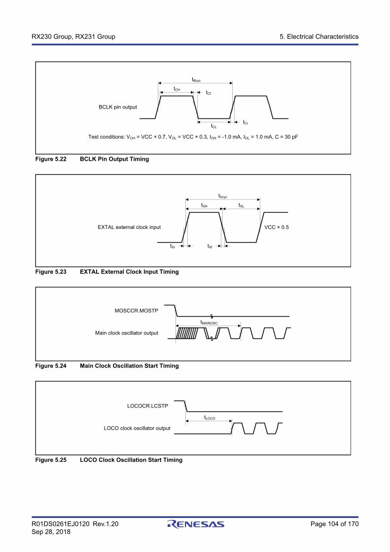
R01DS0261EJ0120 Rev.1.20 Page 104 of 170Sep 28, 2018
RX230 Group, RX231 Group 5. Electrical Characteristics
Figure 5.22 BCLK Pin Output Timing
Figure 5.23 EXTAL External Clock Input Timing
Figure 5.24 Main Clock Oscillation Start Timing
Figure 5.25 LOCO Clock Oscillation Start Timing
tCftCH
tBcyc
tCrtCL
BCLK pin output
Test conditions: VOH = VCC × 0.7, VOL = VCC × 0.3, IOH = -1.0 mA, IOL = 1.0 mA, C = 30 pF
tXH
tXcyc
EXTAL external clock input VCC × 0.5
tXL
tXr tXf
Main clock oscillator output
MOSCCR.MOSTP
tMAINOSC
LOCO clock oscillator output
LOCOCR.LCSTP
tLOCO
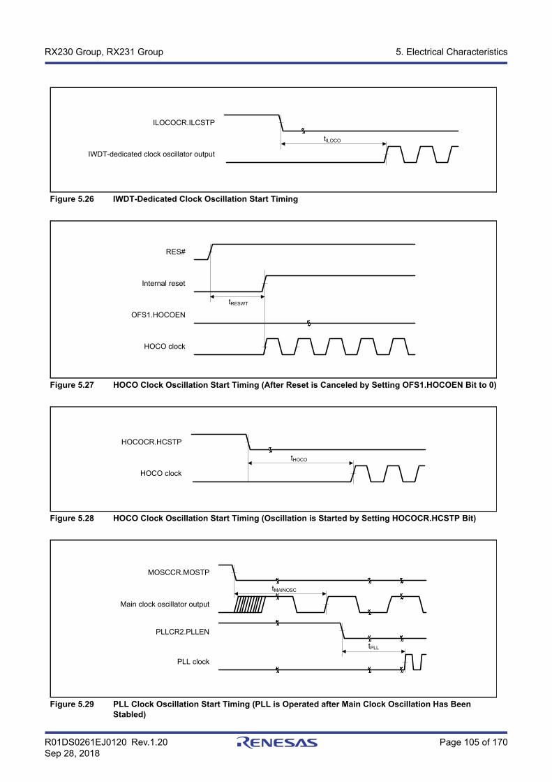
R01DS0261EJ0120 Rev.1.20 Page 105 of 170Sep 28, 2018
RX230 Group, RX231 Group 5. Electrical Characteristics
Figure 5.26 IWDT-Dedicated Clock Oscillation Start Timing
Figure 5.27 HOCO Clock Oscillation Start Timing (After Reset is Canceled by Setting OFS1.HOCOEN Bit to 0)
Figure 5.28 HOCO Clock Oscillation Start Timing (Oscillation is Started by Setting HOCOCR.HCSTP Bit)
Figure 5.29 PLL Clock Oscillation Start Timing (PLL is Operated after Main Clock Oscillation Has Been Stabled)
IWDT-dedicated clock oscillator output
ILOCOCR.ILCSTP
tILOCO
RES#
Internal reset
HOCO clock
OFS1.HOCOEN
tRESWT
HOCO clock
HOCOCR.HCSTP
tHOCO
PLLCR2.PLLEN
PLL clock
MOSCCR.MOSTP
tMAINOSC
Main clock oscillator output
tPLL
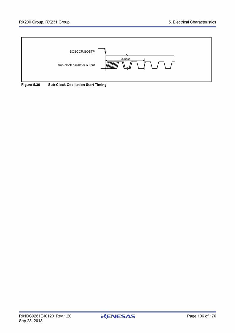
R01DS0261EJ0120 Rev.1.20 Page 106 of 170Sep 28, 2018
RX230 Group, RX231 Group 5. Electrical Characteristics
Figure 5.30 Sub-Clock Oscillation Start Timing
Sub-clock oscillator output
SOSCCR.SOSTP
tSUBOSC
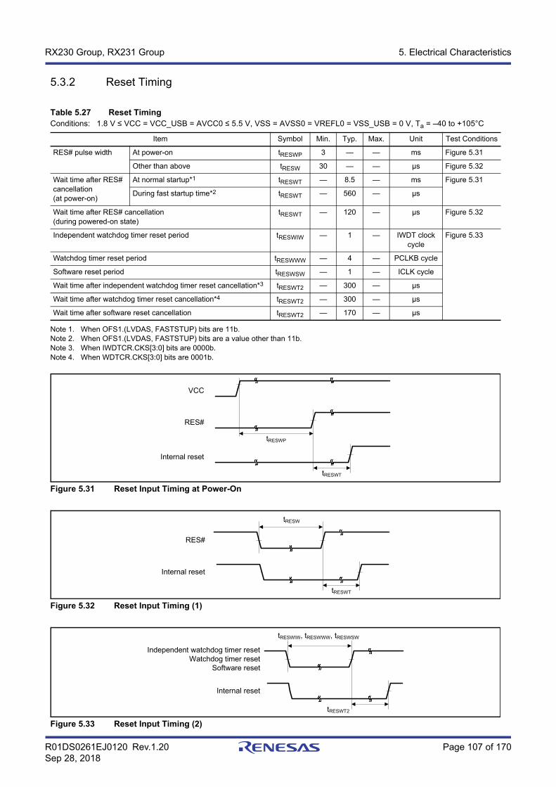
R01DS0261EJ0120 Rev.1.20 Page 107 of 170Sep 28, 2018
RX230 Group, RX231 Group 5. Electrical Characteristics
5.3.2 Reset Timing
Note 1. When OFS1.(LVDAS, FASTSTUP) bits are 11b.Note 2. When OFS1.(LVDAS, FASTSTUP) bits are a value other than 11b.Note 3. When IWDTCR.CKS[3:0] bits are 0000b.Note 4. When WDTCR.CKS[3:0] bits are 0001b.
Figure 5.31 Reset Input Timing at Power-On
Figure 5.32 Reset Input Timing (1)
Figure 5.33 Reset Input Timing (2)
Table 5.27 Reset TimingConditions: 1.8 V ≤ VCC = VCC_USB = AVCC0 ≤ 5.5 V, VSS = AVSS0 = VREFL0 = VSS_USB = 0 V, Ta = –40 to +105°C
Item Symbol Min. Typ. Max. Unit Test Conditions
RES# pulse width At power-on tRESWP 3 — — ms Figure 5.31
Other than above tRESW 30 — — μs Figure 5.32
Wait time after RES# cancellation (at power-on)
At normal startup*1 tRESWT — 8.5 — ms Figure 5.31
During fast startup time*2 tRESWT — 560 — μs
Wait time after RES# cancellation(during powered-on state)
tRESWT — 120 — μs Figure 5.32
Independent watchdog timer reset period tRESWIW — 1 — IWDT clock cycle
Figure 5.33
Watchdog timer reset period tRESWWW — 4 — PCLKB cycle
Software reset period tRESWSW — 1 — ICLK cycle
Wait time after independent watchdog timer reset cancellation*3 tRESWT2 — 300 — μs
Wait time after watchdog timer reset cancellation*4 tRESWT2 — 300 — μs
Wait time after software reset cancellation tRESWT2 — 170 — μs
VCC
RES#
tRESWP
Internal reset
tRESWT
RES#
Internal reset
tRESWT
tRESW
Independent watchdog timer resetWatchdog timer reset
Software reset
Internal reset
tRESWT2
tRESWIW, tRESWWW, tRESWSW
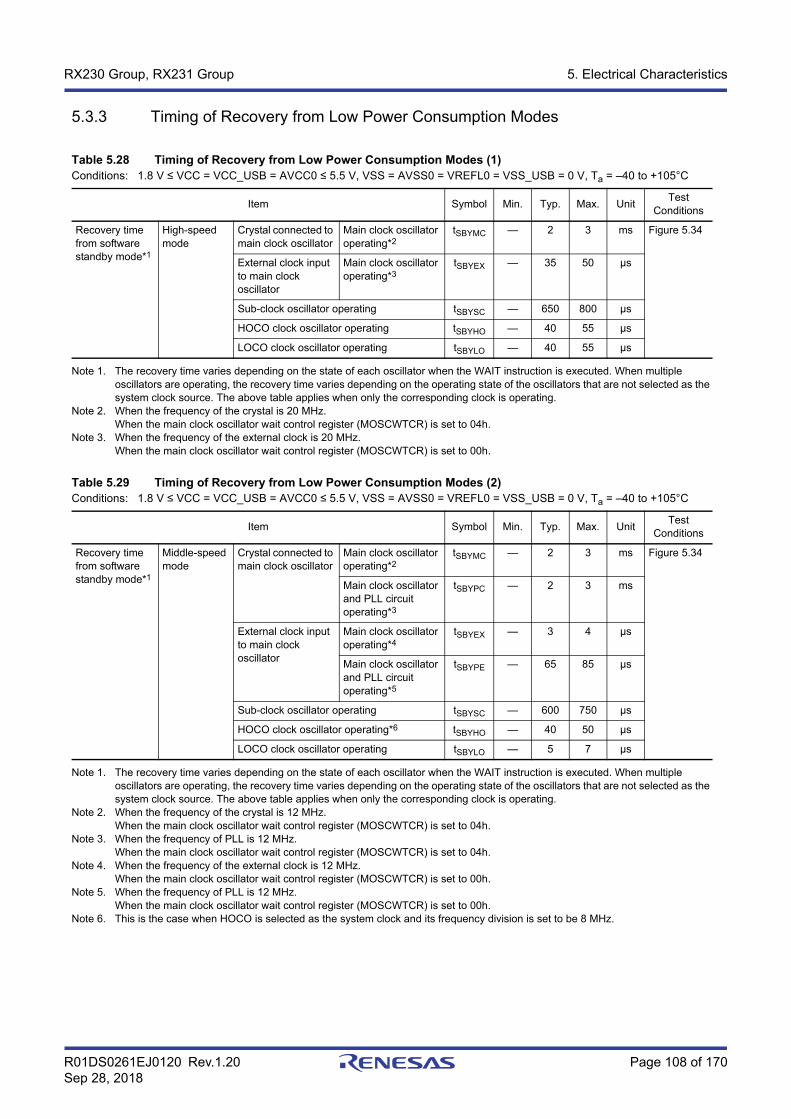
R01DS0261EJ0120 Rev.1.20 Page 108 of 170Sep 28, 2018
RX230 Group, RX231 Group 5. Electrical Characteristics
5.3.3 Timing of Recovery from Low Power Consumption Modes
Note 1. The recovery time varies depending on the state of each oscillator when the WAIT instruction is executed. When multiple oscillators are operating, the recovery time varies depending on the operating state of the oscillators that are not selected as the system clock source. The above table applies when only the corresponding clock is operating.
Note 2. When the frequency of the crystal is 20 MHz.When the main clock oscillator wait control register (MOSCWTCR) is set to 04h.
Note 3. When the frequency of the external clock is 20 MHz.When the main clock oscillator wait control register (MOSCWTCR) is set to 00h.
Note 1. The recovery time varies depending on the state of each oscillator when the WAIT instruction is executed. When multiple oscillators are operating, the recovery time varies depending on the operating state of the oscillators that are not selected as the system clock source. The above table applies when only the corresponding clock is operating.
Note 2. When the frequency of the crystal is 12 MHz.When the main clock oscillator wait control register (MOSCWTCR) is set to 04h.
Note 3. When the frequency of PLL is 12 MHz.When the main clock oscillator wait control register (MOSCWTCR) is set to 04h.
Note 4. When the frequency of the external clock is 12 MHz.When the main clock oscillator wait control register (MOSCWTCR) is set to 00h.
Note 5. When the frequency of PLL is 12 MHz.When the main clock oscillator wait control register (MOSCWTCR) is set to 00h.
Note 6. This is the case when HOCO is selected as the system clock and its frequency division is set to be 8 MHz.
Table 5.28 Timing of Recovery from Low Power Consumption Modes (1)Conditions: 1.8 V ≤ VCC = VCC_USB = AVCC0 ≤ 5.5 V, VSS = AVSS0 = VREFL0 = VSS_USB = 0 V, Ta = –40 to +105°C
Item Symbol Min. Typ. Max. Unit Test Conditions
Recovery time from software standby mode*1
High-speed mode
Crystal connected to main clock oscillator
Main clock oscillator operating*2
tSBYMC — 2 3 ms Figure 5.34
External clock input to main clock oscillator
Main clock oscillator operating*3
tSBYEX — 35 50 μs
Sub-clock oscillator operating tSBYSC — 650 800 μs
HOCO clock oscillator operating tSBYHO — 40 55 μs
LOCO clock oscillator operating tSBYLO — 40 55 μs
Table 5.29 Timing of Recovery from Low Power Consumption Modes (2)Conditions: 1.8 V ≤ VCC = VCC_USB = AVCC0 ≤ 5.5 V, VSS = AVSS0 = VREFL0 = VSS_USB = 0 V, Ta = –40 to +105°C
Item Symbol Min. Typ. Max. Unit Test Conditions
Recovery time from software standby mode*1
Middle-speed mode
Crystal connected to main clock oscillator
Main clock oscillator operating*2
tSBYMC — 2 3 ms Figure 5.34
Main clock oscillator and PLL circuit operating*3
tSBYPC — 2 3 ms
External clock input to main clock oscillator
Main clock oscillator operating*4
tSBYEX — 3 4 μs
Main clock oscillator and PLL circuit operating*5
tSBYPE — 65 85 μs
Sub-clock oscillator operating tSBYSC — 600 750 μs
HOCO clock oscillator operating*6 tSBYHO — 40 50 μs
LOCO clock oscillator operating tSBYLO — 5 7 μs

R01DS0261EJ0120 Rev.1.20 Page 109 of 170Sep 28, 2018
RX230 Group, RX231 Group 5. Electrical Characteristics
Note 1. The sub-clock continues oscillating in software standby mode during low-speed mode.
Figure 5.34 Software Standby Mode Recovery Timing
Note 1. Oscillators continue oscillating in deep sleep mode.Note 2. When the frequency of the system clock is 32 MHz.Note 3. When the frequency of the system clock is 12 MHz.Note 4. When the frequency of the system clock is 32 kHz.
Table 5.30 Timing of Recovery from Low Power Consumption Modes (3)Conditions: 1.8 V ≤ VCC = VCC_USB = AVCC0 ≤ 5.5 V, VSS = AVSS0 = VREFL0 = VSS_USB = 0 V, Ta = –40 to +105°C
Item Symbol Min. Typ. Max. Unit Test Conditions
Recovery time from software standby mode*1
Low-speed mode
Sub-clock oscillator operating tSBYSC — 600 750 μs Figure 5.34
Table 5.31 Timing of Recovery from Low Power Consumption Modes (4)Conditions: 1.8 V ≤ VCC = VCC_USB = AVCC0 ≤ 5.5 V, VSS = AVSS0 = VREFL0 = VSS_USB = 0 V, Ta = –40 to +105°C
Item Symbol Min. Typ. Max. Unit Test Conditions
Recovery time from deep sleep mode*1
High-speed mode*2 tDSLP — 2 3.5 μs Figure 5.35
Middle-speed mode*3 tDSLP — 3 4 μs
Low-speed mode*4 tDSLP — 400 500 μs
Oscillator
ICLK
IRQ
Software standby mode
tSBYMC, tSBYPC, tSBYEX, tSBYPE, tSBYSC, tSBYHO, tSBYLO
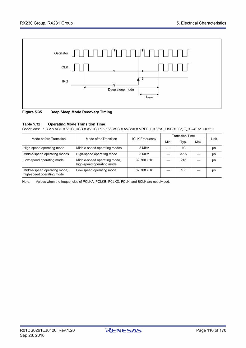
R01DS0261EJ0120 Rev.1.20 Page 110 of 170Sep 28, 2018
RX230 Group, RX231 Group 5. Electrical Characteristics
Figure 5.35 Deep Sleep Mode Recovery Timing
Note: Values when the frequencies of PCLKA, PCLKB, PCLKD, FCLK, and BCLK are not divided.
Table 5.32 Operating Mode Transition TimeConditions: 1.8 V ≤ VCC = VCC_USB = AVCC0 ≤ 5.5 V, VSS = AVSS0 = VREFL0 = VSS_USB = 0 V, Ta = –40 to +105°C
Mode before Transition Mode after Transition ICLK FrequencyTransition Time
UnitMin. Typ. Max.
High-speed operating mode Middle-speed operating modes 8 MHz — 10 — μs
Middle-speed operating modes High-speed operating mode 8 MHz — 37.5 — μs
Low-speed operating mode Middle-speed operating mode, high-speed operating mode
32.768 kHz — 215 — μs
Middle-speed operating mode, high-speed operating mode
Low-speed operating mode 32.768 kHz — 185 — μs
Oscillator
ICLK
IRQ
Deep sleep mode
tDSLP

R01DS0261EJ0120 Rev.1.20 Page 111 of 170Sep 28, 2018
RX230 Group, RX231 Group 5. Electrical Characteristics
5.3.4 Control Signal Timing
Note: 200 ns minimum in software standby mode.Note 1. tPcyc indicates the cycle of PCLKB.Note 2. tNMICK indicates the cycle of the NMI digital filter sampling clock.Note 3. tIRQCK indicates the cycle of the IRQi digital filter sampling clock (i = 0 to 7).
Figure 5.36 NMI Interrupt Input Timing
Figure 5.37 IRQ Interrupt Input Timing
Table 5.33 Control Signal TimingConditions: 1.8 V ≤ VCC = VCC_USB = AVCC0 ≤ 5.5 V, VSS = AVSS0 = VSS_USB = 0 V, Ta = –40 to +105°C
Item Symbol Min. Typ. Max. Unit Test Conditions
NMI pulse width tNMIW 200 — — ns NMI digital filter is disabled (NMIFLTE.NFLTEN = 0)
tPcyc × 2 ≤ 200 ns
tPcyc × 2*1 — — tPcyc × 2 > 200 ns
200 — — NMI digital filter is enabled (NMIFLTE.NFLTEN = 1)
tNMICK × 3 ≤ 200 ns
tNMICK × 3.5*2 — — tNMICK × 3 > 200 ns
IRQ pulse width tIRQW 200 — — ns IRQ digital filter is disabled (IRQFLTE0.FLTENi = 0)
tPcyc × 2 ≤ 200 ns
tPcyc × 2*1 — — tPcyc × 2 > 200 ns
200 — — IRQ digital filter is enabled (IRQFLTE0.FLTENi = 1)
tIRQCK × 3 ≤ 200 ns
tIRQCK × 3.5*3 — — tIRQCK × 3 > 200 ns
NMI
tNMIW
IRQ
tIRQW
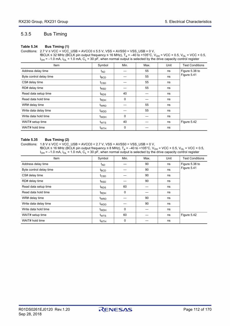
R01DS0261EJ0120 Rev.1.20 Page 112 of 170Sep 28, 2018
RX230 Group, RX231 Group 5. Electrical Characteristics
5.3.5 Bus Timing
Table 5.34 Bus Timing (1)Conditions: 2.7 V ≤ VCC = VCC_USB = AVCC0 ≤ 5.5 V, VSS = AVSS0 = VSS_USB = 0 V,
fBCLK ≤ 32 MHz (BCLK pin output frequency ≤ 16 MHz), Ta = –40 to +105°C, VOH = VCC × 0.5, VOL = VCC × 0.5, IOH = –1.0 mA, IOL = 1.0 mA, CL = 30 pF, when normal output is selected by the drive capacity control register
Item Symbol Min. Max. Unit Test Conditions
Address delay time tAD — 55 ns Figure 5.38 to Figure 5.41Byte control delay time tBCD — 55 ns
CS# delay time tCSD — 55 ns
RD# delay time tRSD — 55 ns
Read data setup time tRDS 40 — ns
Read data hold time tRDH 0 — ns
WR# delay time tWRD — 55 ns
Write data delay time tWDD — 55 ns
Write data hold time tWDH 0 — ns
WAIT# setup time tWTS 40 — ns Figure 5.42
WAIT# hold time tWTH 0 — ns
Table 5.35 Bus Timing (2)Conditions: 1.8 V ≤ VCC = VCC_USB = AVCC0 < 2.7 V, VSS = AVSS0 = VSS_USB = 0 V,
fBCLK ≤ 16 MHz (BCLK pin output frequency ≤ 8 MHz), Ta = –40 to +105°C, VOH = VCC × 0.5, VOL = VCC × 0.5, IOH = –1.0 mA, IOL = 1.0 mA, CL = 30 pF, when normal output is selected by the drive capacity control register
Item Symbol Min. Max. Unit Test Conditions
Address delay time tAD — 90 ns Figure 5.38 to Figure 5.41Byte control delay time tBCD — 90 ns
CS# delay time tCSD — 90 ns
RD# delay time tRSD — 90 ns
Read data setup time tRDS 60 — ns
Read data hold time tRDH 0 — ns
WR# delay time tWRD — 90 ns
Write data delay time tWDD — 90 ns
Write data hold time tWDH 0 — ns
WAIT# setup time tWTS 60 — ns Figure 5.42
WAIT# hold time tWTH 0 — ns
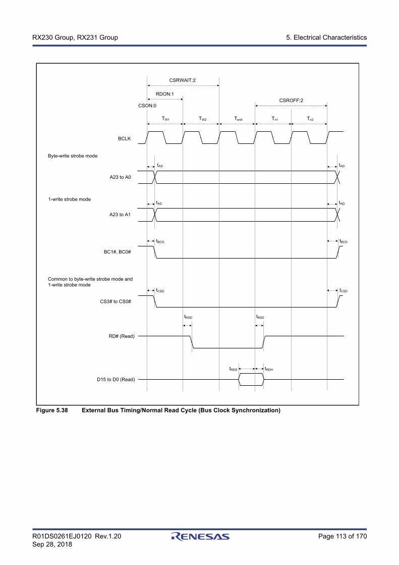
R01DS0261EJ0120 Rev.1.20 Page 113 of 170Sep 28, 2018
RX230 Group, RX231 Group 5. Electrical Characteristics
Figure 5.38 External Bus Timing/Normal Read Cycle (Bus Clock Synchronization)
A23 to A1
CS3# to CS0#
tAD
BCLK
A23 to A0
D15 to D0 (Read)
Byte-write strobe mode
1-write strobe mode
BC1#, BC0#
Common to byte-write strobe mode and 1-write strobe mode
tBCD
tCSD
RD# (Read)
tRSD tRSD
tAD
tRDHtRDS
tAD
tAD
TW1 TW2 Tend Tn1 Tn2
RDON:1
CSRWAIT:2
CSROFF:2CSON:0
tBCD
tCSD
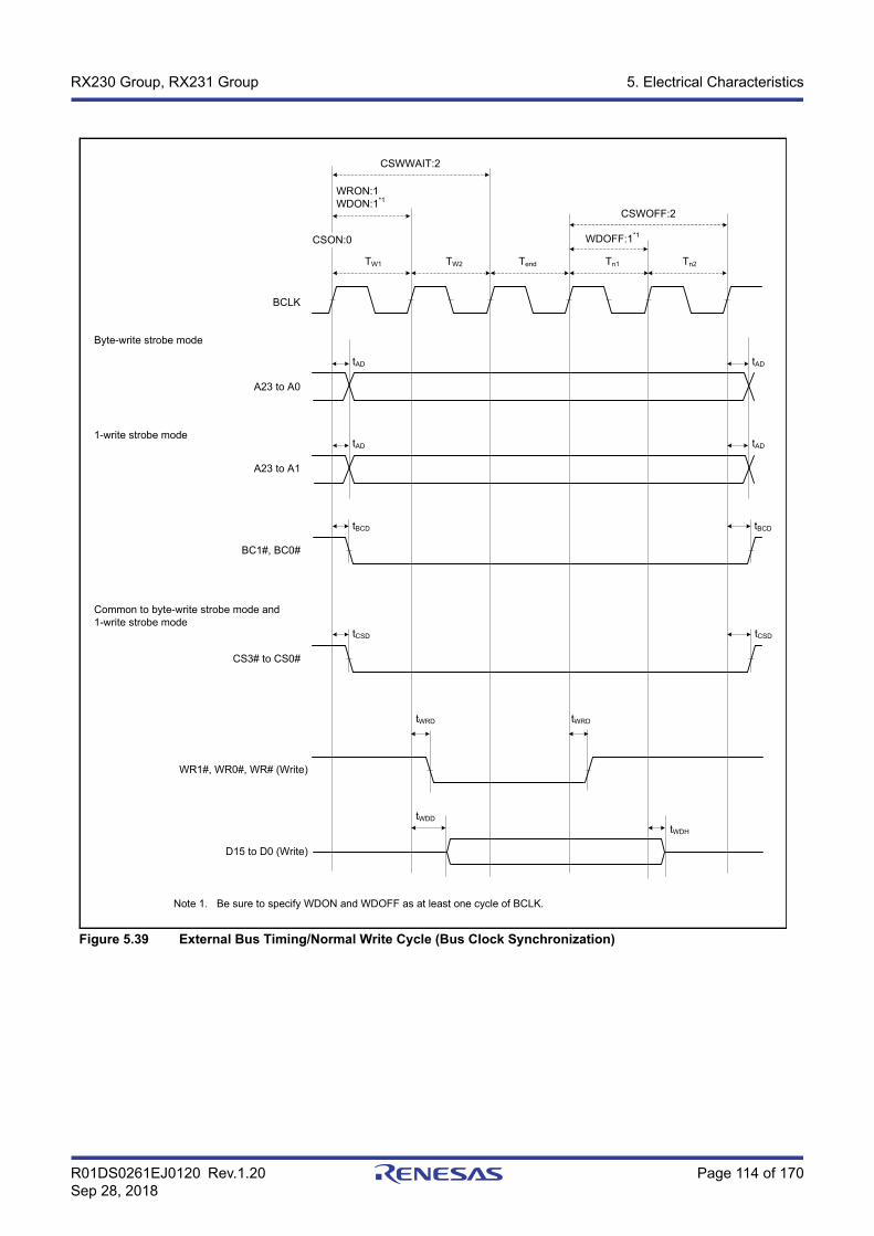
R01DS0261EJ0120 Rev.1.20 Page 114 of 170Sep 28, 2018
RX230 Group, RX231 Group 5. Electrical Characteristics
Figure 5.39 External Bus Timing/Normal Write Cycle (Bus Clock Synchronization)
A23 to A1
CS3# to CS0#
tAD
BCLK
A23 to A0
Byte-write strobe mode
1-write strobe mode
BC1#, BC0#
Common to byte-write strobe mode and 1-write strobe mode
tBCD
tCSD
tAD
tAD
tAD
D15 to D0 (Write)
WR1#, WR0#, WR# (Write)
tWRD tWRD
tWDH
tWDD
TW1 TW2 Tend Tn1 Tn2
WRON:1WDON:1*1
CSWWAIT:2
WDOFF:1*1CSON:0
tBCD
tCSD
CSWOFF:2
Note 1. Be sure to specify WDON and WDOFF as at least one cycle of BCLK.
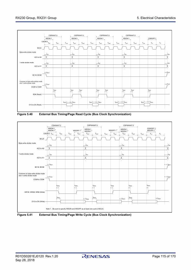
R01DS0261EJ0120 Rev.1.20 Page 115 of 170Sep 28, 2018
RX230 Group, RX231 Group 5. Electrical Characteristics
Figure 5.40 External Bus Timing/Page Read Cycle (Bus Clock Synchronization)
Figure 5.41 External Bus Timing/Page Write Cycle (Bus Clock Synchronization)
A23 to A1
CS3# to CS0#
tAD
BCLK
A23 to A0
D15 to D0 (Read)
Byte-write strobe mode
1-write strobe mode
BC1#, BC0#
Common to byte-write strobe mode and 1-write strobe mode
tBCD
tCSD
RD# (Read)
tRSD tRSD
tRDHtRDS
tAD
TW1 TW2 Tend Tpw1 Tpw2
tAD tAD
tRSD tRSD
tRDHtRDS
tRSD tRSD
tRDHtRDS
Tend Tpw1 Tpw2 Tend Tn1 Th
tAD tAD tAD tAD
RDON:1
CSRWAIT:2
CSROFF:1
tRSD tRSD
tRDHtRDS
tAD
tAD
CSPRWAIT:2
Tpw1 Tpw2 Tend
RDON:1
CSPRWAIT:2
RDON:1
CSPRWAIT:2
RDON:1
CSON:0
tBCD
tCSD
A23 to A1
CS3# to CS0#
tAD
BCLK
A23 to A0
Byte-write strobe mode
1-write strobe mode
BC1#, BC0#
Common to byte-write strobe mode and 1-write strobe mode
tBCD
tCSD
tAD
TW1
D15 to D0 (Write)
WR1#, WR0#, WR# (Write)
tWRD tWRD
tWDHtWDD
TW2 Tend Tpw1 Tpw2
tAD tAD
tWRD tWRD
tWDHtWDD
tWRD tWRD
tWDHtWDD
Tdw1 Tend Tpw1 Tpw2 Tend Tn1 ThTdw1
tAD tAD tAD tAD
WRON:1WDON:1*1
CSWWAIT:2 CSPWWAIT:2
WDOFF:1*1
CSPWWAIT:2
WDOFF:1*1CSWOFF:1WDOFF:1*1
CSON:0
WRON:1WDON:1*1
WRON:1WDON:1*1
tBCD
tCSD
Note 1. Be sure to specify WDON and WDOFF as at least one cycle of BCLK.
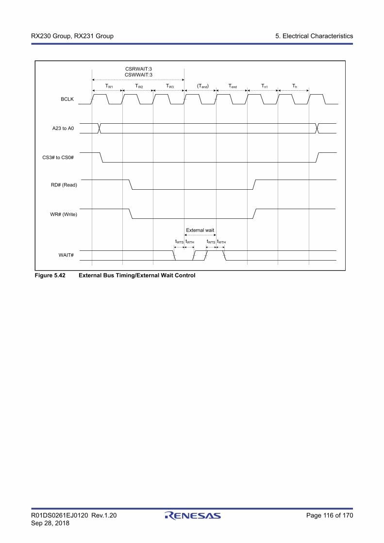
R01DS0261EJ0120 Rev.1.20 Page 116 of 170Sep 28, 2018
RX230 Group, RX231 Group 5. Electrical Characteristics
Figure 5.42 External Bus Timing/External Wait Control
tWTS tWTH tWTS tWTH
CSRWAIT:3CSWWAIT:3
BCLK
A23 to A0
CS3# to CS0#
RD# (Read)
WR# (Write)
WAIT#
TW1 TW2 (Tend) TendTW3 Tn1 Th
External wait

R01DS0261EJ0120 Rev.1.20 Page 117 of 170Sep 28, 2018
RX230 Group, RX231 Group 5. Electrical Characteristics
Table 5.36 Bus Timing (Multiplex bus) (1)Conditions: 2.7 V ≤ VCC = VCC_USB = AVCC0 ≤ 5.5 V, VSS = AVSS0 = VSS_USB = 0 V,
fBCLK ≤ 32 MHz (BCLK pin output frequency ≤ 16 MHz), Ta = –40 to +105°C, VOH = VCC × 0.5, VOL = VCC × 0.5, IOH = –1.0 mA, IOL = 1.0 mA, CL = 30 pF, when normal output is selected by the drive capacity control register
Item Symbol Min. Max. Unit Test Conditions
Address delay time tAD — 55 ns Figure 5.43, Figure 5.44Byte control delay time tBCD — 55 ns
CS# delay time tCSD — 55 ns
RD# delay time tRSD — 55 ns
ALE delay time tALED — 55 ns
Read data setup time tRDS 40 — ns
Read data hold time tRDH 0 — ns
WR# delay time tWRD — 55 ns
Write data delay time tWDD — 55 ns
Write data hold time tWDH 0 — ns
WAIT# setup time tWTS 40 — ns Figure 5.42
WAIT# hold time tWTH 0 — ns
Table 5.37 Bus Timing (Multiplex bus) (2)Conditions: 1.8 V ≤ VCC = VCC_USB = AVCC0 < 5.5 V, VSS = AVSS0 = VSS_USB = 0 V,
fBCLK ≤ 16 MHz (BCLK pin output frequency ≤ 8 MHz), Ta = –40 to +105°C, VOH = VCC × 0.5, VOL = VCC × 0.5, IOH = –1.0 mA, IOL = 1.0 mA, CL = 30 pF, when normal output is selected by the drive capacity control register
Item Symbol Min. Max. Unit Test Conditions
Address delay time tAD — 90 ns Figure 5.43, Figure 5.44Byte control delay time tBCD — 90 ns
CS# delay time tCSD — 90 ns
RD# delay time tRSD — 90 ns
ALE delay time tALED — 90 ns
Read data setup time tRDS 60 — ns
Read data hold time tRDH 0 — ns
WR# delay time tWRD — 90 ns
Write data delay time tWDD — 90 ns
Write data hold time tWDH 0 — ns
WAIT# setup time tWTS 60 — ns Figure 5.42
WAIT# hold time tWTH 0 — ns
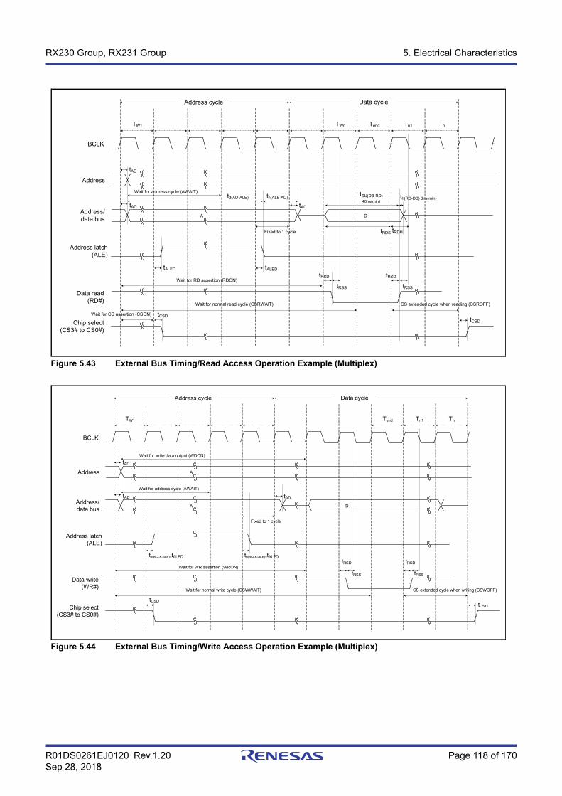
R01DS0261EJ0120 Rev.1.20 Page 118 of 170Sep 28, 2018
RX230 Group, RX231 Group 5. Electrical Characteristics
Figure 5.43 External Bus Timing/Read Access Operation Example (Multiplex)
Figure 5.44 External Bus Timing/Write Access Operation Example (Multiplex)
Address/data bus
Data read (RD#)
tAD
BCLK
Address
Address latch(ALE)
Chip select (CS3# to CS0#)
TW1 TWn
tAD tAD
tSU(DB-RD)40ns(min)
Tend
Address cycle Data cycle
tALED
tCSDtCSD
Tn1 Th
Fixed to 1 cycle
Wait for address cycle (AWAIT)
tRSD
tRSS
tRSD
tRSS
CS extended cycle when reading (CSROFF)
tALED
Wait for RD assertion (RDON)
Wait for normal read cycle (CSRWAIT)
Wait for CS assertion (CSON)
A D
tRDHtRDS
td(AD-ALE) th(ALE-AD) th(RD-DB) 0ns(min)
Address/data bus
Data write(WR#)
tAD
BCLK
Address
Address latch(ALE)
Chip select(CS3# to CS0#)
TW1
tAD tAD
Tend
Address cycle Data cycle
tCSDtCSD
Tn1 Th
Fixed to 1 cycle
td(BCLK-ALE)=tALED
Wait for address cycle (AWAIT)
tRSD
tRSS
tRSD
tRSS
Wait for WR assertion (WRON)
Wait for normal write cycle (CSWWAIT)
A D
Wait for write data output (WDON)
th(BCLK-ALE)=tALED
A
CS extended cycle when writing (CSWOFF)
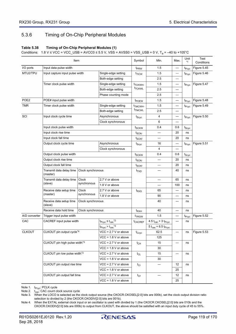
R01DS0261EJ0120 Rev.1.20 Page 119 of 170Sep 28, 2018
RX230 Group, RX231 Group 5. Electrical Characteristics
5.3.6 Timing of On-Chip Peripheral Modules
Note 1. tPcyc: PCLK cycleNote 2. tcac: CAC count clock source cycleNote 3. When the LOCO is selected as the clock output source (the CKOCR.CKOSEL[2:0] bits are 000b), set the clock output division ratio
selection to divided by 2 (the CKOCR.CKODIV[2:0] bits are 001b).Note 4. When the EXTAL external clock input or an oscillator is used with divided by 1 (the CKOCR.CKOSEL[2:0] bits are 010b and the
CKOCR.CKODIV[2:0] bits are 000b) to output from CLKOUT, the above should be satisfied with an input duty cycle of 45 to 55%.
Table 5.38 Timing of On-Chip Peripheral Modules (1)Conditions: 1.8 V ≤ VCC = VCC_USB = AVCC0 ≤ 5.5 V, VSS = AVSS0 = VSS_USB = 0 V, Ta = –40 to +105°C
Item Symbol Min. Max. Unit*1
Test Conditions
I/O ports Input data pulse width tPRW 1.5 — tPcyc Figure 5.45
MTU2/TPU Input capture input pulse width Single-edge setting tTICW 1.5 — tPcyc Figure 5.46
Both-edge setting 2.5 —
Timer clock pulse width Single-edge setting tTCKWH, tTCKWL
1.5 — tPcyc Figure 5.47
Both-edge setting 2.5 —
Phase counting mode 2.5 —
POE2 POE# input pulse width tPOEW 1.5 — tPcyc Figure 5.48
TMR Timer clock pulse width Single-edge setting tTMCWH, tTMCWL
1.5 — tPcyc Figure 5.49
Both-edge setting 2.5 —
SCI Input clock cycle time Asynchronous tScyc 4 — tPcyc Figure 5.50
Clock synchronous 6 —
Input clock pulse width tSCKW 0.4 0.6 tScyc
Input clock rise time tSCKr — 20 ns
Input clock fall time tSCKf — 20 ns
Output clock cycle time Asynchronous tScyc 16 — tPcyc Figure 5.51
Clock synchronous 4 —
Output clock pulse width tSCKW 0.4 0.6 tScyc
Output clock rise time tSCKr — 20 ns
Output clock fall time tSCKf — 20 ns
Transmit data delay time (master)
Clock synchronous tTXD — 40 ns
Transmit data delay time (slave)
Clock synchronous
2.7 V or above — 65 ns
1.8 V or above — 100 ns
Receive data setup time (master)
Clock synchronous
2.7 V or above tRXS 65 — ns
1.8 V or above 90 — ns
Receive data setup time (slave)
Clock synchronous 40 — ns
Receive data hold time Clock synchronous tRXH 40 — ns
A/D converter Trigger input pulse width tTRGW 1.5 — tPcyc Figure 5.52
CAC CACREF input pulse width tPcyc ≤ tcac*2 tCACREF 4.5 tcac + 3 tPcyc — ns
tPcyc > tcac*2 5 tcac + 6.5 tPcyc
CLKOUT CLKOUT pin output cycle*4 VCC = 2.7 V or above tCcyc 62.5 — ns Figure 5.53
VCC = 1.8 V or above 125
CLKOUT pin high pulse width*3 VCC = 2.7 V or above tCH 15 — ns
VCC = 1.8 V or above 30
CLKOUT pin low pulse width*3 VCC = 2.7 V or above tCL 15 — ns
VCC = 1.8 V or above 30
CLKOUT pin output rise time VCC = 2.7 V or above tCr — 12 ns
VCC = 1.8 V or above 25
CLKOUT pin output fall time VCC = 2.7 V or above tCf — 12 ns
VCC = 1.8 V or above 25
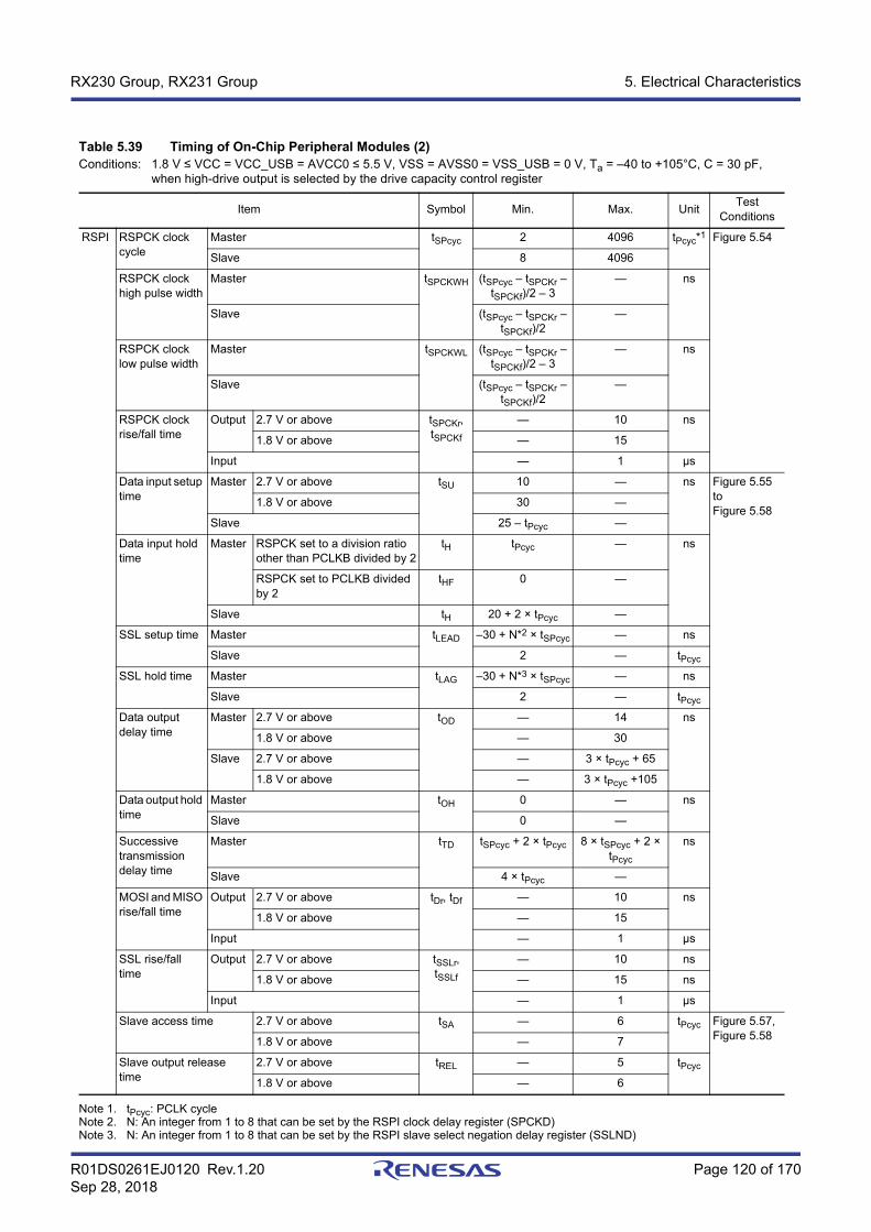
R01DS0261EJ0120 Rev.1.20 Page 120 of 170Sep 28, 2018
RX230 Group, RX231 Group 5. Electrical Characteristics
Note 1. tPcyc: PCLK cycleNote 2. N: An integer from 1 to 8 that can be set by the RSPI clock delay register (SPCKD)Note 3. N: An integer from 1 to 8 that can be set by the RSPI slave select negation delay register (SSLND)
Table 5.39 Timing of On-Chip Peripheral Modules (2)Conditions: 1.8 V ≤ VCC = VCC_USB = AVCC0 ≤ 5.5 V, VSS = AVSS0 = VSS_USB = 0 V, Ta = –40 to +105°C, C = 30 pF,
when high-drive output is selected by the drive capacity control register
Item Symbol Min. Max. Unit Test Conditions
RSPI RSPCK clock cycle
Master tSPcyc 2 4096 tPcyc*1 Figure 5.54
Slave 8 4096
RSPCK clock high pulse width
Master tSPCKWH (tSPcyc – tSPCKr – tSPCKf)/2 – 3
— ns
Slave (tSPcyc – tSPCKr – tSPCKf)/2
—
RSPCK clock low pulse width
Master tSPCKWL (tSPcyc – tSPCKr – tSPCKf)/2 – 3
— ns
Slave (tSPcyc – tSPCKr – tSPCKf)/2
—
RSPCK clock rise/fall time
Output 2.7 V or above tSPCKr, tSPCKf
— 10 ns
1.8 V or above — 15
Input — 1 μs
Data input setup time
Master 2.7 V or above tSU 10 — ns Figure 5.55 to Figure 5.58
1.8 V or above 30 —
Slave 25 – tPcyc —
Data input hold time
Master RSPCK set to a division ratio other than PCLKB divided by 2
tH tPcyc — ns
RSPCK set to PCLKB divided by 2
tHF 0 —
Slave tH 20 + 2 × tPcyc —
SSL setup time Master tLEAD –30 + N*2 × tSPcyc — ns
Slave 2 — tPcyc
SSL hold time Master tLAG –30 + N*3 × tSPcyc — ns
Slave 2 — tPcyc
Data output delay time
Master 2.7 V or above tOD — 14 ns
1.8 V or above — 30
Slave 2.7 V or above — 3 × tPcyc + 65
1.8 V or above — 3 × tPcyc +105
Data output hold time
Master tOH 0 — ns
Slave 0 —
Successive transmission delay time
Master tTD tSPcyc + 2 × tPcyc 8 × tSPcyc + 2 × tPcyc
ns
Slave 4 × tPcyc —
MOSI and MISO rise/fall time
Output 2.7 V or above tDr, tDf — 10 ns
1.8 V or above — 15
Input — 1 μs
SSL rise/fall time
Output 2.7 V or above tSSLr, tSSLf
— 10 ns
1.8 V or above — 15 ns
Input — 1 μs
Slave access time 2.7 V or above tSA — 6 tPcyc Figure 5.57, Figure 5.581.8 V or above — 7
Slave output release time
2.7 V or above tREL — 5 tPcyc
1.8 V or above — 6
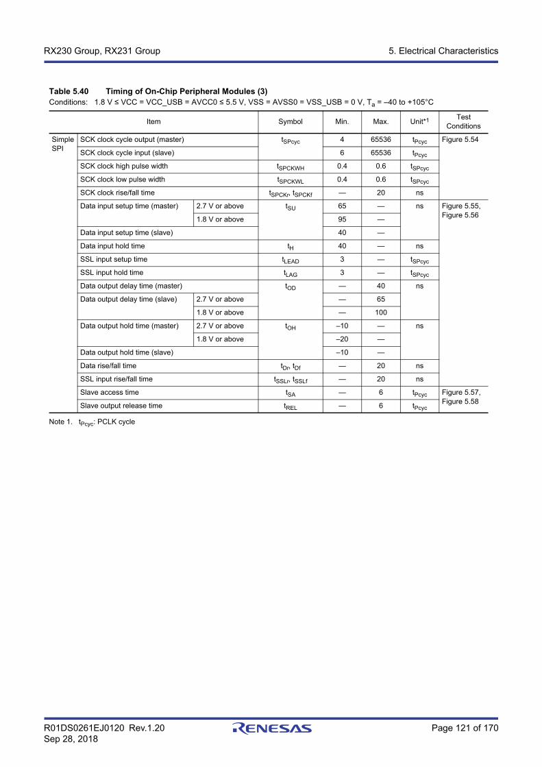
R01DS0261EJ0120 Rev.1.20 Page 121 of 170Sep 28, 2018
RX230 Group, RX231 Group 5. Electrical Characteristics
Note 1. tPcyc: PCLK cycle
Table 5.40 Timing of On-Chip Peripheral Modules (3)Conditions: 1.8 V ≤ VCC = VCC_USB = AVCC0 ≤ 5.5 V, VSS = AVSS0 = VSS_USB = 0 V, Ta = –40 to +105°C
Item Symbol Min. Max. Unit*1 Test Conditions
Simple SPI
SCK clock cycle output (master) tSPcyc 4 65536 tPcyc Figure 5.54
SCK clock cycle input (slave) 6 65536 tPcyc
SCK clock high pulse width tSPCKWH 0.4 0.6 tSPcyc
SCK clock low pulse width tSPCKWL 0.4 0.6 tSPcyc
SCK clock rise/fall time tSPCKr, tSPCKf — 20 ns
Data input setup time (master) 2.7 V or above tSU 65 — ns Figure 5.55, Figure 5.561.8 V or above 95 —
Data input setup time (slave) 40 —
Data input hold time tH 40 — ns
SSL input setup time tLEAD 3 — tSPcyc
SSL input hold time tLAG 3 — tSPcyc
Data output delay time (master) tOD — 40 ns
Data output delay time (slave) 2.7 V or above — 65
1.8 V or above — 100
Data output hold time (master) 2.7 V or above tOH –10 — ns
1.8 V or above –20 —
Data output hold time (slave) –10 —
Data rise/fall time tDr, tDf — 20 ns
SSL input rise/fall time tSSLr, tSSLf — 20 ns
Slave access time tSA — 6 tPcyc Figure 5.57, Figure 5.58Slave output release time tREL — 6 tPcyc
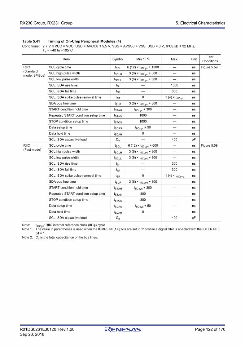
R01DS0261EJ0120 Rev.1.20 Page 122 of 170Sep 28, 2018
RX230 Group, RX231 Group 5. Electrical Characteristics
Note: tIICcyc: RIIC internal reference clock (IICφ) cycleNote 1. The value in parentheses is used when the ICMR3.NF[1:0] bits are set to 11b while a digital filter is enabled with the ICFER.NFE
bit = 1.Note 2. Cb is the total capacitance of the bus lines.
Table 5.41 Timing of On-Chip Peripheral Modules (4)Conditions: 2.7 V ≤ VCC = VCC_USB = AVCC0 ≤ 5.5 V, VSS = AVSS0 = VSS_USB = 0 V, fPCLKB ≤ 32 MHz,
Ta = –40 to +105°C
Item Symbol Min.*1, *2 Max. Unit Test Conditions
RIIC(Standard mode, SMBus)
SCL cycle time tSCL 6 (12) × tIICcyc + 1300 — ns Figure 5.59
SCL high pulse width tSCLH 3 (6) × tIICcyc + 300 — ns
SCL low pulse width tSCLL 3 (6) × tIICcyc + 300 — ns
SCL, SDA rise time tSr — 1000 ns
SCL, SDA fall time tSf — 300 ns
SCL, SDA spike pulse removal time tSP 0 1 (4) × tIICcyc ns
SDA bus free time tBUF 3 (6) × tIICcyc + 300 — ns
START condition hold time tSTAH tIICcyc + 300 — ns
Repeated START condition setup time tSTAS 1000 — ns
STOP condition setup time tSTOS 1000 — ns
Data setup time tSDAS tIICcyc + 50 — ns
Data hold time tSDAH 0 — ns
SCL, SDA capacitive load Cb — 400 pF
RIIC(Fast mode)
SCL cycle time tSCL 6 (12) × tIICcyc + 600 — ns Figure 5.59
SCL high pulse width tSCLH 3 (6) × tIICcyc + 300 — ns
SCL low pulse width tSCLL 3 (6) × tIICcyc + 300 — ns
SCL, SDA rise time tSr — 300 ns
SCL, SDA fall time tSf — 300 ns
SCL, SDA spike pulse removal time tSP 0 1 (4) × tIICcyc ns
SDA bus free time tBUF 3 (6) × tIICcyc + 300 — ns
START condition hold time tSTAH tIICcyc + 300 — ns
Repeated START condition setup time tSTAS 300 — ns
STOP condition setup time tSTOS 300 — ns
Data setup time tSDAS tIICcyc + 50 — ns
Data hold time tSDAH 0 — ns
SCL, SDA capacitive load Cb — 400 pF

R01DS0261EJ0120 Rev.1.20 Page 123 of 170Sep 28, 2018
RX230 Group, RX231 Group 5. Electrical Characteristics
Note: tPcyc: PCLK cycleNote 1. Cb is the total capacitance of the bus lines.
Table 5.42 Timing of On-Chip Peripheral Modules (5)Conditions: 2.7 V ≤ VCC = VCC_USB = AVCC0 ≤ 5.5 V, VSS = AVSS0 = VSS_USB = 0 V, fPCLKB ≤ 32 MHz,
Ta = –40 to +105°C
Item Symbol Min.*1 Max. Unit Test Conditions
Simple I2C(Standard mode)
SDA rise time tSr — 1000 ns Figure 5.59
SDA fall time tSf — 300 ns
SDA spike pulse removal time tSP 0 4 × tPcyc ns
Data setup time tSDAS 250 — ns
Data hold time tSDAH 0 — ns
SCL, SDA capacitive load Cb — 400 pF
Simple I2C(Fast mode)
SDA rise time tSr — 300 ns Figure 5.59
SDA fall time tSf — 300 ns
SDA spike pulse removal time tSP 0 4 × tPcyc ns
Data setup time tSDAS 100 — ns
Data hold time tSDAH 0 — ns
SCL, SDA capacitive load Cb — 400 pF
Table 5.43 Timing of On-Chip Peripheral Modules (6)Conditions: 1.8 V ≤ VCC = VCC_USB = AVCC0 ≤ 5.5 V, VSS = AVSS0 = VSS_USB = 0 V, fPCLKB ≤ 32 MHz,
Ta = –40 to +105°C
Item Symbol Min. Max. Unit Test Conditions
SSI AUDIO_MCLK input frequency
2.7 V or above tAUDIO 1 25 MHz
1.8 V or above 1 4
Output clock cycle tO 250 — ns Figure 5.60
Input clock cycle tI 250 — ns
Clock high level tHC 0.4 0.6 to, ti
Clock low level tLC 0.4 0.6 to, ti
Clock rise time tRC — 20 ns
Data delay time 2.7 V or above tDTR — 65 ns Figure 5.61Figure 5.621.8 V or above — 105
Setup time 2.7 V or above tSR 65 — ns
1.8 V or above 90 —
Hold time tHTR 40 — ns
WS changing edge SSIDATA output delay tDTRW — 105 ns Figure 5.63

R01DS0261EJ0120 Rev.1.20 Page 124 of 170Sep 28, 2018
RX230 Group, RX231 Group 5. Electrical Characteristics
Table 5.44 Timing of On-Chip Peripheral Modules (7)Conditions: 2.7 V ≤ VCC = VCC_USB = AVCC0 ≤ 3.6 V, VSS = AVSS0 = VSS_USB = 0 V, fPCLKB ≤ 32 MHz,
Ta = –40 to +105°C, when high-drive output is selected by the drive capacity control register
Item Symbol Min. Max. Unit Test Conditions
SDHI SDHI_CLK pin output cycle time tPP(SD) 62.5 — ns Figure 5.64
SDHI_CLK pin output high pulse width tWH(SD) 18.25 — ns
SDHI_CLK pin output low pulse width tWL(SD) 18.25 — ns
SDHI_CLK pin output rise time tTLH(SD) — 10 ns
SDHI_CLK pin output fall time tTHL(SD) — 10 ns
Output data delay time (data transfer mode) for SDHI_CMD and SDHI_D0 to SDHI_D3 pins
tODLY(SD) –18.25 18.25 ns
Input data setup time for SDHI_CMD and SDHI_D0 to SDHI_D3 pins
tISU(SD) 9.25 — ns
Input data hold time for SDHI_CMD and SDHI_D0 to SDHI_D3 pins
tIH(SD) 8.3 — ns
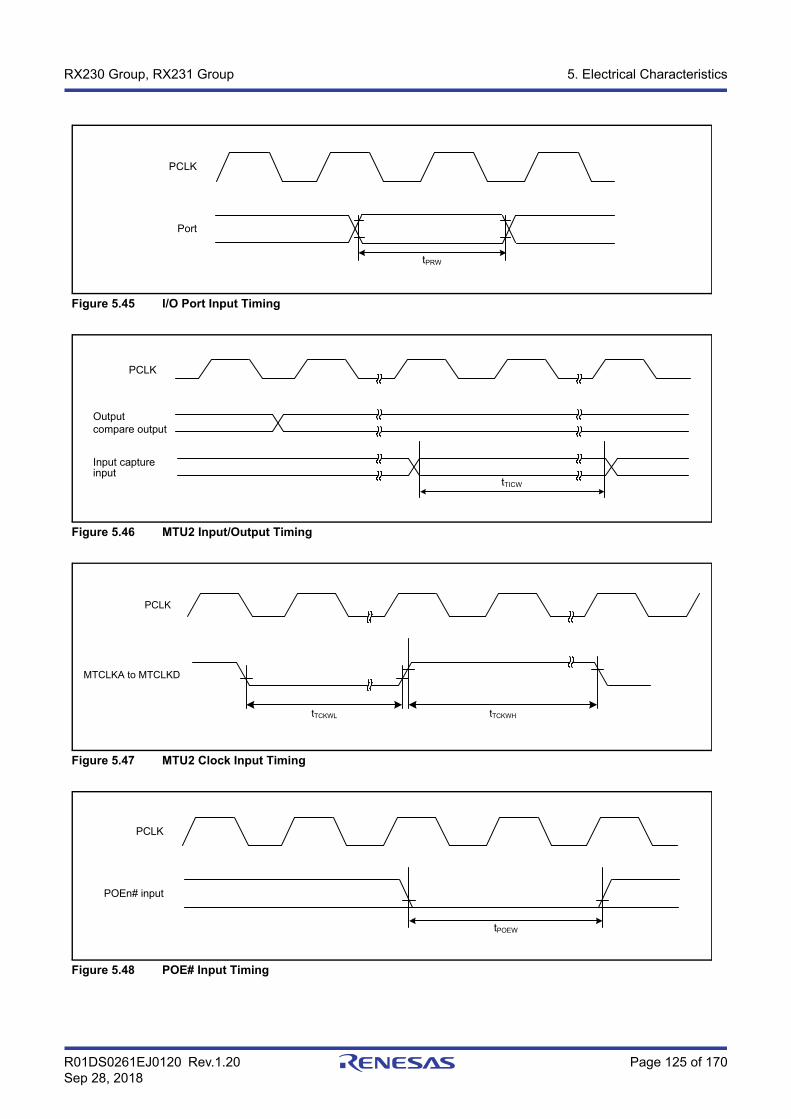
R01DS0261EJ0120 Rev.1.20 Page 125 of 170Sep 28, 2018
RX230 Group, RX231 Group 5. Electrical Characteristics
Figure 5.45 I/O Port Input Timing
Figure 5.46 MTU2 Input/Output Timing
Figure 5.47 MTU2 Clock Input Timing
Figure 5.48 POE# Input Timing
Port
PCLK
tPRW
Output compare output
Input capture input
PCLK
tTICW
MTCLKA to MTCLKD
PCLK
tTCKWL tTCKWH
POEn# input
PCLK
tPOEW

R01DS0261EJ0120 Rev.1.20 Page 126 of 170Sep 28, 2018
RX230 Group, RX231 Group 5. Electrical Characteristics
Figure 5.49 TMR Clock Input Timing
Figure 5.50 SCK Clock Input Timing
Figure 5.51 SCI Input/Output Timing: Clock Synchronous Mode
PCLK
TMCI0 to TMCI3
tTMCWL tTMCWH
tSCKW tSCKr tSCKf
tScyc
SCKn
n = 0, 1, 5, 6, 8, 9, 12
tTXD
tRXS tRXH
TXDn
RXDn
SCKn
n = 0, 1, 5, 6, 8, 9, 12

R01DS0261EJ0120 Rev.1.20 Page 127 of 170Sep 28, 2018
RX230 Group, RX231 Group 5. Electrical Characteristics
Figure 5.52 A/D Converter External Trigger Input Timing
Figure 5.53 CLKOUT Output Timing
Figure 5.54 RSPI Clock Timing and Simple SPI Clock Timing
ADTRG0#
PCLK
tTRGW
tCftCH
tCcyc
tCrtCL
CLKOUT pin output
Test conditions: VOH = VCC × 0.7, VOL = VCC × 0.3, IOH = -1.0 mA, IOL = 1.0 mA, C = 30 pF
tSPCKWH
VOH VOH
VOL VOL
VOH VOH
tSPCKWL
tSPCKr tSPCKf
VOL
tSPcyc
tSPCKWH
VIH VIH
VIL VIL
VIH VIH
tSPCKWL
tSPCKr tSPCKf
VIL
tSPcyc
VOH = 0.7 × VCC, VOL = 0.3 × VCC, VIH = 0.7 × VCC, VIL = 0.3 × VCC
n = 0, 1, 5, 6, 8, 9, 12
SCKnMaster select output
SCKnSlave select input
RSPCKAMaster select output
RSPCKASlave select input
Simple SPIRSPI
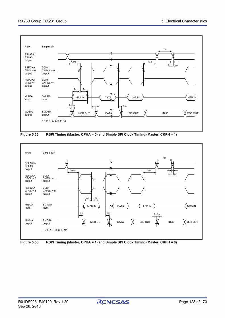
R01DS0261EJ0120 Rev.1.20 Page 128 of 170Sep 28, 2018
RX230 Group, RX231 Group 5. Electrical Characteristics
Figure 5.55 RSPI Timing (Master, CPHA = 0) and Simple SPI Clock Timing (Master, CKPH = 1)
Figure 5.56 RSPI Timing (Master, CPHA = 1) and Simple SPI Clock Timing (Master, CKPH = 0)
tDr, tDf
tSU tH
tLEAD
tTD
tLAG
tSSLr, tSSLf
tOH tOD
MSB IN DATA LSB IN MSB IN
MSB OUT DATA LSB OUT IDLE MSB OUT
SCKnCKPOL = 0output
SCKnCKPOL = 1output
SMISOninput
SMOSInoutput
n = 0, 1, 5, 6, 8, 9, 12
Simple SPIRSPI
SSLA0 to SSLA3output
RSPCKACPOL = 0output
RSPCKACPOL = 1output
MISOAinput
MOSIAoutput
SSLA0 to SSLA3output
RSPCKACPOL = 0output
RSPCKACPOL = 1output
MISOAinput
MOSIAoutput
RSPI Simple SPI
SCKnCKPOL = 1output
SCKnCKPOL = 0output
SMISOninput
SMOSInoutput
tDr, tDf
tSU tH
tLEAD
tTD
tLAG
tSSLr, tSSLf
tOH
MSB IN DATA LSB IN MSB IN
MSB OUT DATA LSB OUT IDLE MSB OUT
tOD
n = 0, 1, 5, 6, 8, 9, 12

R01DS0261EJ0120 Rev.1.20 Page 129 of 170Sep 28, 2018
RX230 Group, RX231 Group 5. Electrical Characteristics
Figure 5.57 RSPI Timing (Slave, CPHA = 0) and Simple SPI Clock Timing (Slave, CKPH = 1)
Figure 5.58 RSPI Timing (Slave, CPHA = 1) and Simple SPI Clock Timing (Slave, CKPH = 0)
tDr, tDftSU tH
tLEAD
tTD
tLAG
tSA
MSB IN DATA LSB IN MSB IN
MSB OUT DATA LSB OUT MSB IN MSB OUT
tOH tOD tREL
SCKnCKPOL = 0input
SCKnCKPOL = 1input
SMISOnoutput
SMOSIninput
n = 0, 1, 5, 6, 8, 9, 12
Simple SPIRSPI
SSLA0input
RSPCKACPOL = 0input
RSPCKACPOL = 1input
MISOAoutput
MOSIAinput
SSn#input
tDr, tDf
tSA tOH
tLEAD
tTD
tLAG
tH
LSB OUT(Last data) DATA MSB OUT
MSB IN DATA LSB IN MSB IN
LSB OUT
tSU
tOD tREL
MSB OUT
SCKnCKPOL = 1input
SCKnCKPOL = 0input
SMISOnoutput
SMOSIninput
n = 0, 1, 5, 6, 8, 9, 12
Simple SPIRSPI
SSLA0input
RSPCKACPOL = 0input
RSPCKACPOL = 1input
MISOAoutput
MOSIAinput
SSn#input
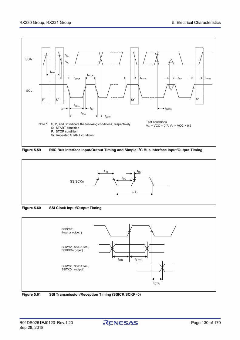
R01DS0261EJ0120 Rev.1.20 Page 130 of 170Sep 28, 2018
RX230 Group, RX231 Group 5. Electrical Characteristics
Figure 5.59 RIIC Bus Interface Input/Output Timing and Simple I2C Bus Interface Input/Output Timing
Figure 5.60 SSI Clock Input/Output Timing
Figure 5.61 SSI Transmission/Reception Timing (SSICR.SCKP=0)
Test conditionsVIH = VCC × 0.7, VIL = VCC × 0.3
SDA
SCL
VIH
VIL
tSTAH
tSCLH
tSCLL
P*1 S*1
tSf tSr
tSCLtSDAH
tSDAS
tSTAS tSP tSTOS
P*1
tBUF
Sr*1
Note 1. S, P, and Sr indicate the following conditions, respectively.S: START conditionP: STOP conditionSr: Repeated START condition
SSISCKn
tHC
tLC
tRC
tI, tO
tSR tHTR
tDTR
SSISCKn(input or output )
SSIWSn, SSIDATAn , SSIRXDn (input)
SSIWSn, SSIDATAn , SSITXDn (output )
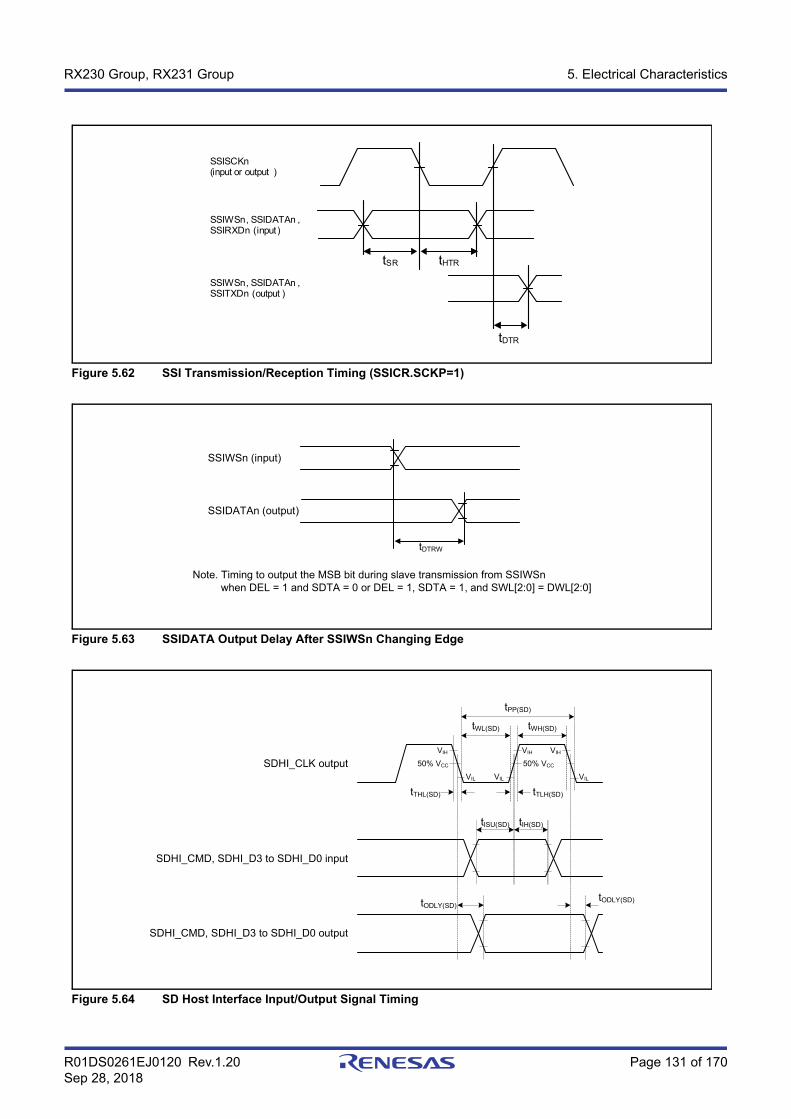
R01DS0261EJ0120 Rev.1.20 Page 131 of 170Sep 28, 2018
RX230 Group, RX231 Group 5. Electrical Characteristics
Figure 5.62 SSI Transmission/Reception Timing (SSICR.SCKP=1)
Figure 5.63 SSIDATA Output Delay After SSIWSn Changing Edge
Figure 5.64 SD Host Interface Input/Output Signal Timing
tSR tHTR
tDTR
SSISCKn(input or output )
SSIWSn, SSIDATAn , SSIRXDn (input)
SSIWSn, SSIDATAn , SSITXDn (output )
tDTRW
SSIWSn (input)
SSIDATAn (output)
Note. Timing to output the MSB bit during slave transmission from SSIWSn when DEL = 1 and SDTA = 0 or DEL = 1, SDTA = 1, and SWL[2:0] = DWL[2:0]
SDHI_CLK output
SDHI_CMD, SDHI_D3 to SDHI_D0 input
SDHI_CMD, SDHI_D3 to SDHI_D0 output
tWL(SD) tWH(SD)
tPP(SD)
tISU(SD) tIH(SD)
tTLH(SD)tTHL(SD)
tODLY(SD)tODLY(SD)
VIH
VIL VIL VIL
VIH VIH
50% VCC 50% VCC

R01DS0261EJ0120 Rev.1.20 Page 132 of 170Sep 28, 2018
RX230 Group, RX231 Group 5. Electrical Characteristics
5.4 USB Characteristics
Figure 5.65 USB0_DP and USB0_DM Output Timing
Table 5.45 USB Characteristics (USB0_DP and USB0_DM Pin Characteristics)Conditions: 3.0 V ≤ VCC = VCC_USB = AVCC < 3.6 V (when a regulator is not in use) or 4.0 V ≤ VCC = AVCC0 < 5.5 V (when
a regulator is in use), VSS = AVSS0 = VSS_USB = 0 V, Ta = –40 to +105°C
Item Symbol Min. Max. Unit Test Conditions
Input characteristics
Input high level voltage VIH 2.0 — V
Input low level voltage VIL — 0.8 V
Differential input sensitivity VDI 0.2 — V | USB0_DP – USB0_DM |
Differential common mode range
VCM 0.8 2.5 V
Output characteristics
Output high level voltage VOH 2.8 VCC_USB V IOH = –200 μA
Output low level voltage VOL 0.0 0.3 V IOL = 2 mA
Cross-over voltage VCRS 1.3 2.0 V Figure 5.65, Figure 5.66Rise time FS tr 4 20 ns
LS 75 300
Fall time FS tf 4 20 ns
LS 75 300
Rise/fall time ratio FS tr/tf 90 111.11 % tr/tfLS 80 125
Output resistance ZDRV 28 44 Ω (Adjusting the resistance by external elements is not necessary.)
VBUS characteristics
VBUS input voltage VIH VCC × 0.8 — V
VIL — VCC × 0.2 V
Pull-up, pull-down
Pull-down resistor RPD 14.25 24.80 kΩ
Pull-up resistor RPUI 0.9 1.575 kΩ During idle state
RPUA 1.425 3.09 kΩ During reception
Battery Charging Specification Ver 1.2
D+ sink current IDP_SINK 25 175 μA
D- sink current IDM_SINK 25 175 μA
DCD source current IDP_SRC 7 13 μA
Data detection voltage VDAT_REF 0.25 0.4 V
D+ source current VDP_SRC 0.5 0.7 V Output current = 250 μA
D- source current VDM_SRC 0.5 0.7 V Output current = 250 μA
USB0_DP, USB0_DM
tftr
90%10%10%
90%VCRS
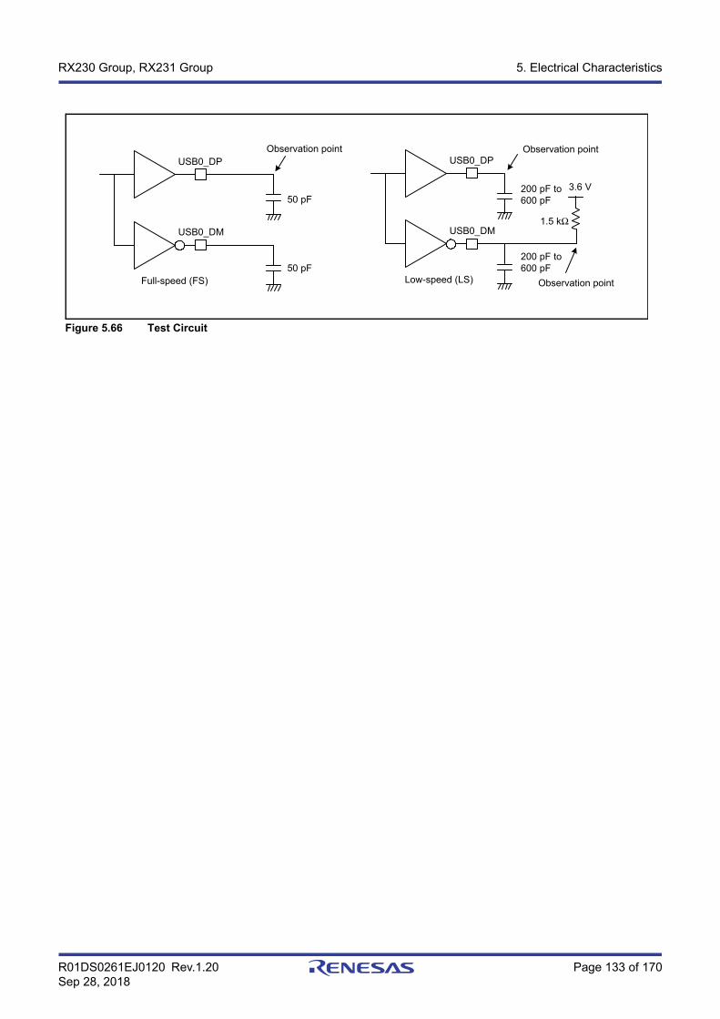
R01DS0261EJ0120 Rev.1.20 Page 133 of 170Sep 28, 2018
RX230 Group, RX231 Group 5. Electrical Characteristics
Figure 5.66 Test Circuit
Observation point
50 pF
50 pF
USB0_DP
USB0_DM
Full-speed (FS)
Observation point
1.5 kΩ
200 pF to 600 pF
USB0_DP
USB0_DM
200 pF to600 pF
3.6 V
Observation pointLow-speed (LS)

R01DS0261EJ0120 Rev.1.20 Page 134 of 170Sep 28, 2018
RX230 Group, RX231 Group 5. Electrical Characteristics
5.5 A/D Conversion Characteristics
Figure 5.67 VREFH0 Voltage Range vs. AVCC0
Note: The characteristics apply when no pin functions other than A/D converter input are used. Absolute accuracy includes quantization errors. Offset error, full-scale error, DNL differential non-linearity error, and INL integral non-linearity error do not include quantization errors.
Note 1. The conversion time is the sum of the sampling time and the comparison time. As the test conditions, the number of sampling states is indicated.
Table 5.46 A/D Conversion Characteristics (1)Conditions: 2.7 V ≤ VCC = VCC_USB = AVCC0 ≤ 5.5 V, 2.7 V ≤ VREFH0 ≤ AVCC0, reference voltage = VREFH0 selected,
VSS = AVSS0 = VREFL0 = VSS_USB = 0 V, Ta = –40 to +105°C
Item Min. Typ. Max. Unit Test Conditions
Frequency 1 — 54 MHz
Resolution — — 12 Bit
Conversion time*1
(Operation at PCLKD = 54 MHz)
Permissible signal source impedance (Max.) = 0.3 kΩ
0.83 — — μs High-precision channelThe ADCSR.ADHSC bit is 0The ADSSTRn register is 0Dh
1.33 — — Normal-precision channelThe ADCSR.ADHSC bit is 0The ADSSTRn register is 28h
Analog input capacitance Cs — — 15 pF Pin capacitance includedFigure 5.68
Analog input resistance Rs — — 2.5 kΩ Figure 5.68
Analog input voltage range Ain 0 — VREFH0 V
Offset error — ±0.5 ±4.5 LSB High-precision channel
±6.0 LSB Other than above
Full-scale error — ±0.75 ±4.5 LSB High-precision channel
±6.0 LSB Other than above
Quantization error — ± 0.5 — LSB
Absolute accuracy — ± 1.25 ±5.0 LSB High-precision channel
±8.0 LSB Other than above
DNL differential non-linearity error — ±1.0 — LSB
INL integral non-linearity error — ±1.0 ±3.0 LSB
VREFH0
5.0
4.0
3.0
2.0
1.0
1.0 2.0 3.0 4.0 5.0
A/D Conversion Characteristics (1)
A/D Conversion Characteristics (2)
ADCSR.ADHSC = 0
5.5
2.72.4
2.4 2.7 5.5 AVCC0
VREFH0
5.0
4.0
3.0
2.0
1.0
1.0 2.0 3.0 4.0 5.0
A/D Conversion Characteristics (3)
A/D Conversion Characteristics (4)
ADCSR.ADHSC = 1
5.5
2.72.4
2.4 2.7 5.5 AVCC0
A/D Conversion Characteristics (5)1.8
1.8
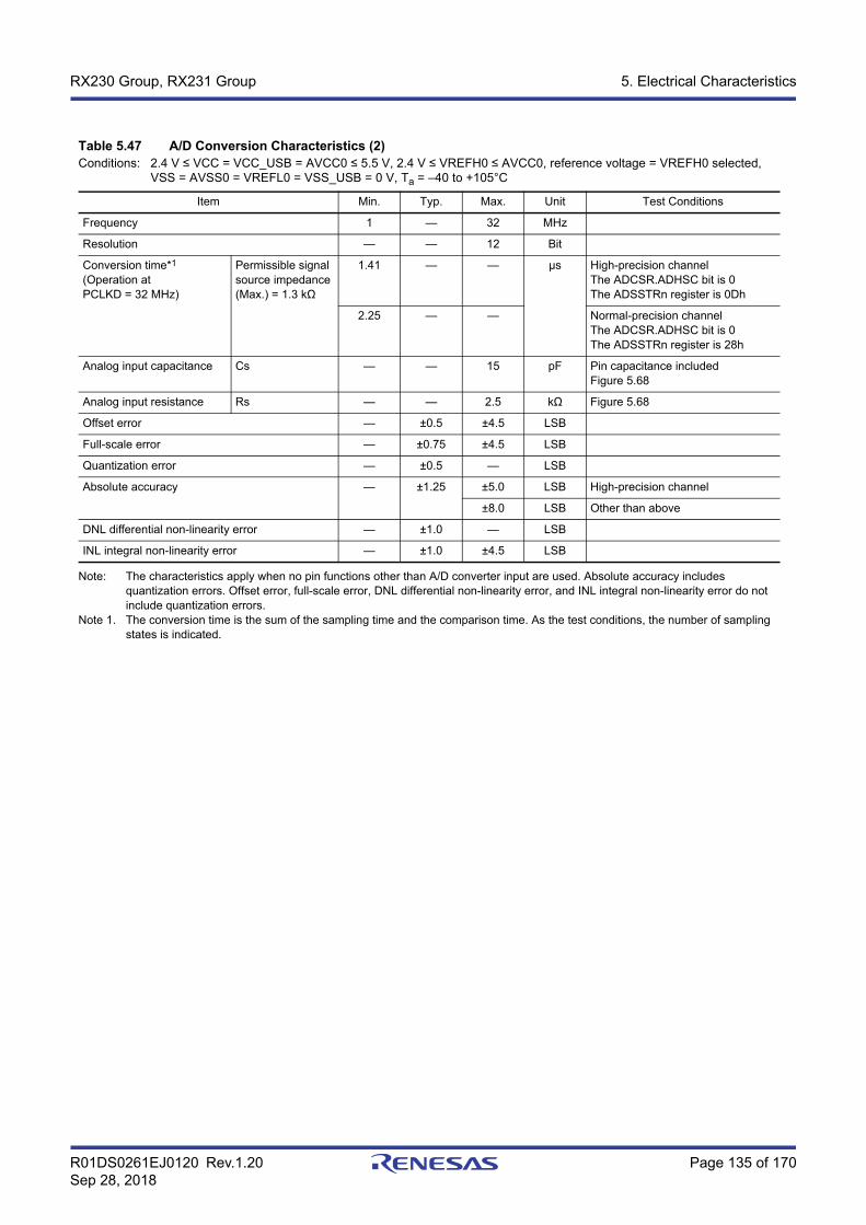
R01DS0261EJ0120 Rev.1.20 Page 135 of 170Sep 28, 2018
RX230 Group, RX231 Group 5. Electrical Characteristics
Note: The characteristics apply when no pin functions other than A/D converter input are used. Absolute accuracy includes quantization errors. Offset error, full-scale error, DNL differential non-linearity error, and INL integral non-linearity error do not include quantization errors.
Note 1. The conversion time is the sum of the sampling time and the comparison time. As the test conditions, the number of sampling states is indicated.
Table 5.47 A/D Conversion Characteristics (2)Conditions: 2.4 V ≤ VCC = VCC_USB = AVCC0 ≤ 5.5 V, 2.4 V ≤ VREFH0 ≤ AVCC0, reference voltage = VREFH0 selected,
VSS = AVSS0 = VREFL0 = VSS_USB = 0 V, Ta = –40 to +105°C
Item Min. Typ. Max. Unit Test Conditions
Frequency 1 — 32 MHz
Resolution — — 12 Bit
Conversion time*1
(Operation at PCLKD = 32 MHz)
Permissible signal source impedance (Max.) = 1.3 kΩ
1.41 — — μs High-precision channelThe ADCSR.ADHSC bit is 0The ADSSTRn register is 0Dh
2.25 — — Normal-precision channelThe ADCSR.ADHSC bit is 0The ADSSTRn register is 28h
Analog input capacitance Cs — — 15 pF Pin capacitance includedFigure 5.68
Analog input resistance Rs — — 2.5 kΩ Figure 5.68
Offset error — ±0.5 ±4.5 LSB
Full-scale error — ±0.75 ±4.5 LSB
Quantization error — ±0.5 — LSB
Absolute accuracy — ±1.25 ±5.0 LSB High-precision channel
±8.0 LSB Other than above
DNL differential non-linearity error — ±1.0 — LSB
INL integral non-linearity error — ±1.0 ±4.5 LSB
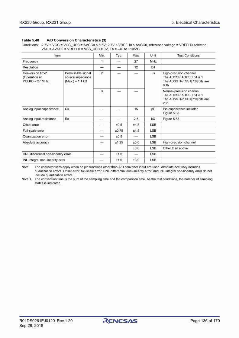
R01DS0261EJ0120 Rev.1.20 Page 136 of 170Sep 28, 2018
RX230 Group, RX231 Group 5. Electrical Characteristics
Note: The characteristics apply when no pin functions other than A/D converter input are used. Absolute accuracy includes quantization errors. Offset error, full-scale error, DNL differential non-linearity error, and INL integral non-linearity error do not include quantization errors.
Note 1. The conversion time is the sum of the sampling time and the comparison time. As the test conditions, the number of sampling states is indicated.
Table 5.48 A/D Conversion Characteristics (3)Conditions: 2.7V ≤ VCC = VCC_USB = AVCC0 ≤ 5.5V, 2.7V ≤ VREFH0 ≤ AVCC0, reference voltage = VREFH0 selected,
VSS = AVSS0 = VREFL0 = VSS_USB = 0V, Ta = –40 to +105°C
Item Min. Typ. Max. Unit Test Conditions
Frequency 1 — 27 MHz
Resolution — — 12 Bit
Conversion time*1
(Operation at PCLKD = 27 MHz)
Permissible signal source impedance (Max.) = 1.1 kΩ
2 — — μs High-precision channelThe ADCSR.ADHSC bit is 1The ADSSTRn.SST[7:0] bits are 0Dh
3 — — Normal-precision channelThe ADCSR.ADHSC bit is 1The ADSSTRn.SST[7:0] bits are 28h
Analog input capacitance Cs — — 15 pF Pin capacitance includedFigure 5.68
Analog input resistance Rs — — 2.5 kΩ Figure 5.68
Offset error — ±0.5 ±4.5 LSB
Full-scale error — ±0.75 ±4.5 LSB
Quantization error — ±0.5 — LSB
Absolute accuracy — ±1.25 ±5.0 LSB High-precision channel
±8.0 LSB Other than above
DNL differential non-linearity error — ±1.0 — LSB
INL integral non-linearity error — ±1.0 ±3.0 LSB

R01DS0261EJ0120 Rev.1.20 Page 137 of 170Sep 28, 2018
RX230 Group, RX231 Group 5. Electrical Characteristics
Note: The characteristics apply when no pin functions other than A/D converter input are used. Absolute accuracy includes quantization errors. Offset error, full-scale error, DNL differential non-linearity error, and INL integral non-linearity error do not include quantization errors.
Note 1. The conversion time is the sum of the sampling time and the comparison time. As the test conditions, the number of sampling states is indicated.
Table 5.49 A/D Conversion Characteristics (4)Conditions: 2.4V ≤ VCC = VCC_USB = AVCC0 ≤ 5.5V, 2.4V ≤ VREFH0 ≤ AVCC0, VSS = AVSS0 = VSS_USB = 0V,
reference voltage = VREFH0 selected, Ta = –40 to +105°C
Item Min. Typ. Max. Unit Test Conditions
Frequency 1 — 16 MHz
Resolution — — 12 Bit
Conversion time*1
(Operation at PCLKD = 16 MHz)
Permissible signal source impedance (Max.) = 2.2 kΩ
3.38 — — μs High-precision channelThe ADCSR.ADHSC bit is 1The ADSSTRn register is 0Dh
5.06 — — Normal-precision channelThe ADCSR.ADHSC bit is 1The ADSSTRn register is 28h
Analog input capacitance Cs — — 15 pF Pin capacitance includedFigure 5.68
Analog input resistance Rs — — 2.5 kΩ Figure 5.68
Offset error — ±0.5 ±4.5 LSB
Full-scale error — ±0.75 ±4.5 LSB
Quantization error — ±0.5 — LSB
Absolute accuracy — ±1.25 ±5.0 LSB High-precision channel
±8.0 LSB Other than above
DNL differential non-linearity error — ±1.0 — LSB
INL integral non-linearity error — ±1.0 ±3.0 LSB
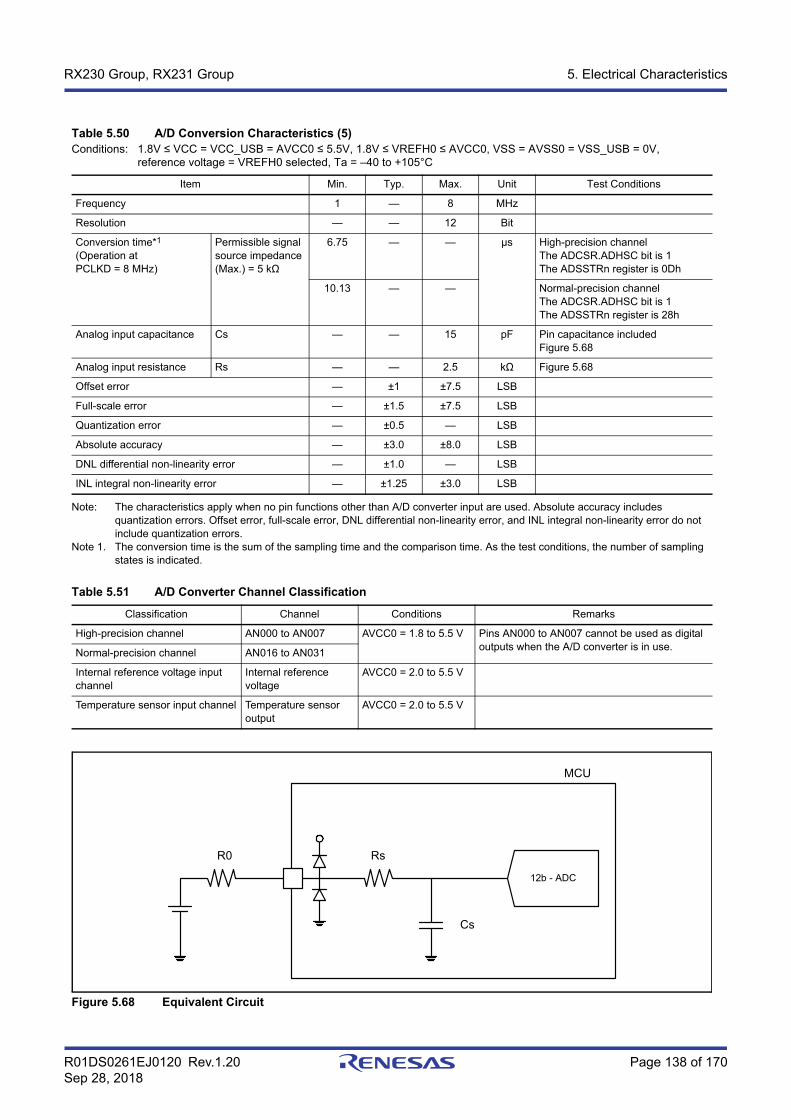
R01DS0261EJ0120 Rev.1.20 Page 138 of 170Sep 28, 2018
RX230 Group, RX231 Group 5. Electrical Characteristics
Note: The characteristics apply when no pin functions other than A/D converter input are used. Absolute accuracy includes quantization errors. Offset error, full-scale error, DNL differential non-linearity error, and INL integral non-linearity error do not include quantization errors.
Note 1. The conversion time is the sum of the sampling time and the comparison time. As the test conditions, the number of sampling states is indicated.
Figure 5.68 Equivalent Circuit
Table 5.50 A/D Conversion Characteristics (5)Conditions: 1.8V ≤ VCC = VCC_USB = AVCC0 ≤ 5.5V, 1.8V ≤ VREFH0 ≤ AVCC0, VSS = AVSS0 = VSS_USB = 0V,
reference voltage = VREFH0 selected, Ta = –40 to +105°C
Item Min. Typ. Max. Unit Test Conditions
Frequency 1 — 8 MHz
Resolution — — 12 Bit
Conversion time*1
(Operation at PCLKD = 8 MHz)
Permissible signal source impedance (Max.) = 5 kΩ
6.75 — — μs High-precision channelThe ADCSR.ADHSC bit is 1The ADSSTRn register is 0Dh
10.13 — — Normal-precision channelThe ADCSR.ADHSC bit is 1The ADSSTRn register is 28h
Analog input capacitance Cs — — 15 pF Pin capacitance includedFigure 5.68
Analog input resistance Rs — — 2.5 kΩ Figure 5.68
Offset error — ±1 ±7.5 LSB
Full-scale error — ±1.5 ±7.5 LSB
Quantization error — ±0.5 — LSB
Absolute accuracy — ±3.0 ±8.0 LSB
DNL differential non-linearity error — ±1.0 — LSB
INL integral non-linearity error — ±1.25 ±3.0 LSB
Table 5.51 A/D Converter Channel Classification
Classification Channel Conditions Remarks
High-precision channel AN000 to AN007 AVCC0 = 1.8 to 5.5 V Pins AN000 to AN007 cannot be used as digital outputs when the A/D converter is in use.Normal-precision channel AN016 to AN031
Internal reference voltage input channel
Internal reference voltage
AVCC0 = 2.0 to 5.5 V
Temperature sensor input channel Temperature sensor output
AVCC0 = 2.0 to 5.5 V
12b - ADC
Cs
RsR0
MCU

R01DS0261EJ0120 Rev.1.20 Page 139 of 170Sep 28, 2018
RX230 Group, RX231 Group 5. Electrical Characteristics
Figure 5.69 Illustration of A/D Converter Characteristic Terms
Absolute accuracyAbsolute accuracy is the difference between output code based on the theoretical A/D conversion characteristics and the actual A/D conversion result. When measuring absolute accuracy, the voltage at the midpoint of the width of analog input voltage (1-LSB width), that can meet the expectation of outputting an equal code based on the theoretical A/D conversion characteristics, is used as an analog input voltage. For example, if 12-bit resolution is used and if reference voltage (VREFH0 = 3.072 V), then 1-LSB width becomes 0.75 mV, and 0 mV, 0.75 mV, 1.5 mV, ... are used as analog input voltages.If analog input voltage is 6 mV, absolute accuracy = ±5 LSB means that the actual A/D conversion result is in the range of 003h to 00Dh, although an output code, 008h, can be expected from the theoretical A/D conversion characteristics.
Integral non-linearity error (INL)The integral non-linearity error is the maximum deviation between the ideal line when the measured offset and full-scale errors are zeroed, and the actual output code.
Integral nonlinearity error (INL)
Actual A/D conversion characteristic
Ideal A/D conversion characteristic
Analog input voltage
Offset error
Absolute accuracy
Differential nonlinearity error (DNL)
Full-scale errorFFFh
000h
0
Ideal line of actual A/D conversion characteristic
1-LSB width for ideal A/D conversion characteristic
Differential nonlinearity error (DNL)
1-LSB width for ideal A/D conversion characteristic
VREFH0(full-scale)
A/D converteroutput code
R01DS0261EJ0120 Rev.1.20 Page 140 of 170Sep 28, 2018
RX230 Group, RX231 Group 5. Electrical Characteristics
Differential non-linearity error (DNL)The differential non-linearity error is the difference between 1-LSB width based on the ideal A/D conversion characteristics and the width of the actual output code.
Offset errorAn offset error is the difference between a transition point of the ideal first output code and the actual first output code.
Full-scale errorA full-scale error is the difference between a transition point of the ideal last output code and the actual last output code.
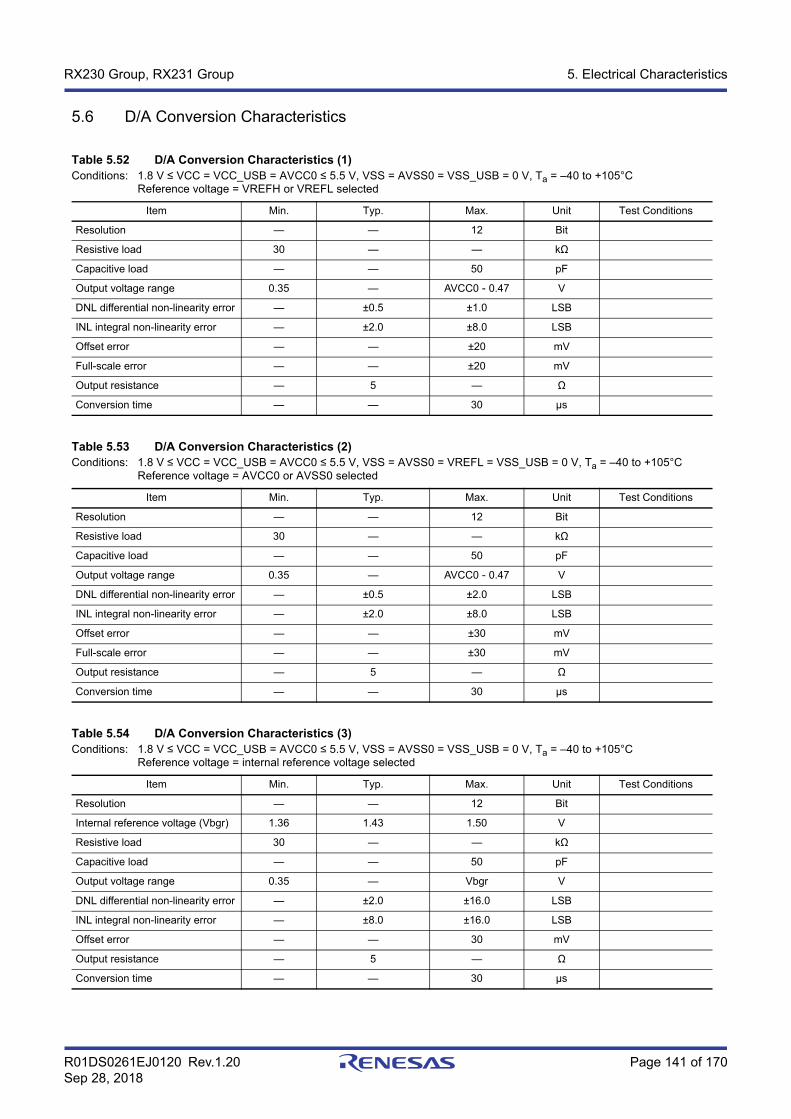
R01DS0261EJ0120 Rev.1.20 Page 141 of 170Sep 28, 2018
RX230 Group, RX231 Group 5. Electrical Characteristics
5.6 D/A Conversion Characteristics
Table 5.52 D/A Conversion Characteristics (1)Conditions: 1.8 V ≤ VCC = VCC_USB = AVCC0 ≤ 5.5 V, VSS = AVSS0 = VSS_USB = 0 V, Ta = –40 to +105°C
Reference voltage = VREFH or VREFL selected
Item Min. Typ. Max. Unit Test Conditions
Resolution — — 12 Bit
Resistive load 30 — — kΩ
Capacitive load — — 50 pF
Output voltage range 0.35 — AVCC0 - 0.47 V
DNL differential non-linearity error — ±0.5 ±1.0 LSB
INL integral non-linearity error — ±2.0 ±8.0 LSB
Offset error — — ±20 mV
Full-scale error — — ±20 mV
Output resistance — 5 — Ω
Conversion time — — 30 μs
Table 5.53 D/A Conversion Characteristics (2)Conditions: 1.8 V ≤ VCC = VCC_USB = AVCC0 ≤ 5.5 V, VSS = AVSS0 = VREFL = VSS_USB = 0 V, Ta = –40 to +105°C
Reference voltage = AVCC0 or AVSS0 selected
Item Min. Typ. Max. Unit Test Conditions
Resolution — — 12 Bit
Resistive load 30 — — kΩ
Capacitive load — — 50 pF
Output voltage range 0.35 — AVCC0 - 0.47 V
DNL differential non-linearity error — ±0.5 ±2.0 LSB
INL integral non-linearity error — ±2.0 ±8.0 LSB
Offset error — — ±30 mV
Full-scale error — — ±30 mV
Output resistance — 5 — Ω
Conversion time — — 30 μs
Table 5.54 D/A Conversion Characteristics (3)Conditions: 1.8 V ≤ VCC = VCC_USB = AVCC0 ≤ 5.5 V, VSS = AVSS0 = VSS_USB = 0 V, Ta = –40 to +105°C
Reference voltage = internal reference voltage selected
Item Min. Typ. Max. Unit Test Conditions
Resolution — — 12 Bit
Internal reference voltage (Vbgr) 1.36 1.43 1.50 V
Resistive load 30 — — kΩ
Capacitive load — — 50 pF
Output voltage range 0.35 — Vbgr V
DNL differential non-linearity error — ±2.0 ±16.0 LSB
INL integral non-linearity error — ±8.0 ±16.0 LSB
Offset error — — 30 mV
Output resistance — 5 — Ω
Conversion time — — 30 μs

R01DS0261EJ0120 Rev.1.20 Page 142 of 170Sep 28, 2018
RX230 Group, RX231 Group 5. Electrical Characteristics
Figure 5.70 Illustration of D/A Converter Characteristic Terms
Integral non-linearity error (INL)The integral non-linearity error is the maximum deviation between the ideal line when the measured offset and full-scale errors are zeroed, and the actual output code.
Differential non-linearity error (DNL)The differential non-linearity error is the difference between 1-LSB width based on the ideal D/A conversion characteristics and the width of the actually output code.
Offset errorAn offset error is the difference between a transition point of the ideal first output code and the actual first output code.
Full-scale errorA full-scale error is the difference between a transition point of the ideal last output code and the actual last output code.
000hD/A converter input code
FFFh
Output analog voltage
Upper output limit
Lower output limit
Offset error
Ideal output voltage
1-LSB width for ideal D/A conversion characteristic
Differential nonlinearity error (DNL)
Actual D/A conversion characteristic
*1
Integral nonlinearity error (INL)
Full-scale error Gain error
Offset error
Ideal output voltage
Note 1. Ideal D/A conversion output voltage that is adjusted so that offset and full scale errors are zeroed.

R01DS0261EJ0120 Rev.1.20 Page 143 of 170Sep 28, 2018
RX230 Group, RX231 Group 5. Electrical Characteristics
5.7 Temperature Sensor Characteristics
5.8 Comparator Characteristics
Table 5.55 Temperature Sensor CharacteristicsConditions: 2.0 V ≤ VCC = VCC_USB = AVCC0 ≤ 5.5 V, VSS = AVSS0 = VSS_USB = 0 V, Ta = –40 to +105°C
Item Symbol Min. Typ. Max. Unit Test Conditions
Relative accuracy ― ― ±1.5 ― °C 2.4 V or above
― ±2.0 ― Below 2.4 V
Temperature slope ― ― –3.65 ― mV/°C
Output voltage (25°C) ― ― 1.05 ― V VCC = 3.3 V
Temperature sensor start time tSTART ― ― 5 μs
Sampling time ― 5 ― ― μs
Table 5.56 Comparator CharacteristicsConditions: 1.8 V ≤ VCC = VCC_USB = AVCC0 ≤ 5.5 V, VSS = AVSS0 = VSS_USB = 0 V, Ta = –40 to +105°C
Item Symbol Min. Typ. Max. Unit Test Conditions
CVREFB0 to CVREFB3 input reference voltage
VREF 0 — VCC - 1.4 V
CMPB0 to CMPB3 input voltage VI –0.3 — VCC + 0.3 V
Offset Comparator high-speed mode
— — — 50 mV
Comparator high-speed modeWindow function enabled
— — — 60 mV
Comparator low-speed mode
— — — 40 mV
Comparator output delay time
Comparator high-speed mode
Td — — 1.2 μs VCC = 3 V, input slew rate ≥ 50 mV/us
Comparator high-speed modeWindow function enabled
Tdw — — 2.0 μs
Comparator low-speed mode
Td — — 5.0 μs
High-side reference voltage(comparator high-speed mode, window function enabled)
VRFH — 0.76 VCC — V
Low-side reference voltage(comparator high-speed mode, window function enabled)
VRFL — 0.24 VCC — V
Operation stabilization wait time Tcmp 100 — — μs
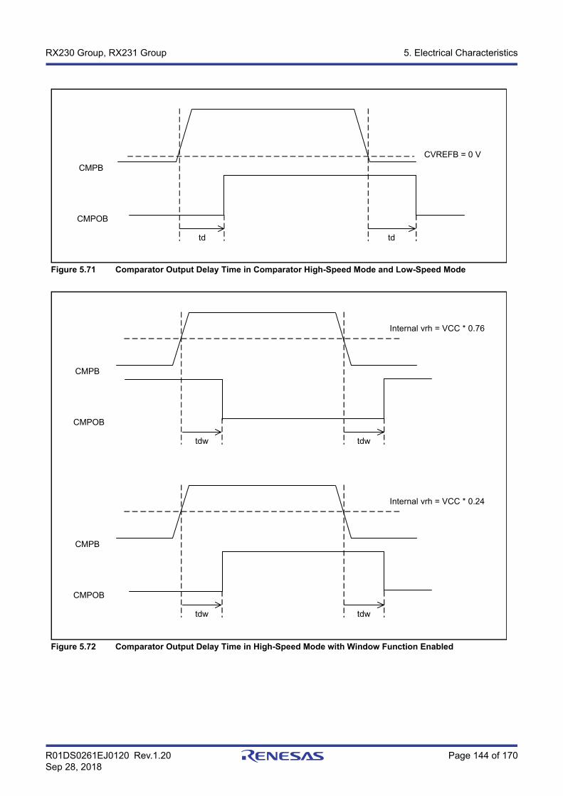
R01DS0261EJ0120 Rev.1.20 Page 144 of 170Sep 28, 2018
RX230 Group, RX231 Group 5. Electrical Characteristics
Figure 5.71 Comparator Output Delay Time in Comparator High-Speed Mode and Low-Speed Mode
Figure 5.72 Comparator Output Delay Time in High-Speed Mode with Window Function Enabled
CMPB
CMPOB
td td
CVREFB = 0 V
CMPB
CMPOB
tdw tdw
Internal vrh = VCC * 0.76
CMPB
CMPOB
tdw tdw
Internal vrh = VCC * 0.24
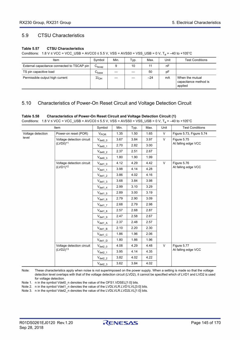
R01DS0261EJ0120 Rev.1.20 Page 145 of 170Sep 28, 2018
RX230 Group, RX231 Group 5. Electrical Characteristics
5.9 CTSU Characteristics
5.10 Characteristics of Power-On Reset Circuit and Voltage Detection Circuit
Note: These characteristics apply when noise is not superimposed on the power supply. When a setting is made so that the voltage detection level overlaps with that of the voltage detection circuit (LVD2), it cannot be specified which of LVD1 and LVD2 is used for voltage detection.
Note 1. n in the symbol Vdet0_n denotes the value of the OFS1.VDSEL[1:0] bits.Note 2. n in the symbol Vdet1_n denotes the value of the LVDLVLR.LVD1LVL[3:0] bits.Note 3. n in the symbol Vdet2_n denotes the value of the LVDLVLR.LVD2LVL[1:0] bits.
Table 5.57 CTSU CharacteristicsConditions: 1.8 V ≤ VCC = VCC_USB = AVCC0 ≤ 5.5 V, VSS = AVSS0 = VSS_USB = 0 V, Ta = –40 to +105°C
Item Symbol Min. Typ. Max. Unit Test Conditions
External capacitance connected to TSCAP pin Ctscap 9 10 11 nF
TS pin capacitive load Cbase — — 50 pF
Permissible output high current ΣIOH — — –24 mA When the mutual capacitance method is applied
Table 5.58 Characteristics of Power-On Reset Circuit and Voltage Detection Circuit (1)Conditions: 1.8 V ≤ VCC = VCC_USB = AVCC0 ≤ 5.5 V, VSS = AVSS0 = VSS_USB = 0 V, Ta = –40 to +105°C
Item Symbol Min. Typ. Max. Unit Test Conditions
Voltage detection level
Power-on reset (POR) VPOR 1.35 1.50 1.65 V Figure 5.73, Figure 5.74
Voltage detection circuit (LVD0)*1
Vdet0_0 3.67 3.84 3.97 V Figure 5.75At falling edge VCCVdet0_1 2.70 2.82 3.00
Vdet0_2 2.37 2.51 2.67
Vdet0_3 1.80 1.90 1.99
Voltage detection circuit (LVD1)*2
Vdet1_0 4.12 4.29 4.42 V Figure 5.76At falling edge VCCVdet1_1 3.98 4.14 4.28
Vdet1_2 3.86 4.02 4.16
Vdet1_3 3.68 3.84 3.98
Vdet1_4 2.99 3.10 3.29
Vdet1_5 2.89 3.00 3.19
Vdet1_6 2.79 2.90 3.09
Vdet1_7 2.68 2.79 2.98
Vdet1_8 2.57 2.68 2.87
Vdet1_9 2.47 2.58 2.67
Vdet1_A 2.37 2.48 2.57
Vdet1_B 2.10 2.20 2.30
Vdet1_C 1.86 1.96 2.06
Vdet1_D 1.80 1.86 1.96
Voltage detection circuit (LVD2)*3
Vdet2_0 4.08 4.29 4.48 V Figure 5.77At falling edge VCCVdet2_1 3.95 4.14 4.35
Vdet2_2 3.82 4.02 4.22
Vdet2_3 3.62 3.84 4.02
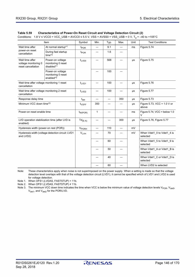
R01DS0261EJ0120 Rev.1.20 Page 146 of 170Sep 28, 2018
RX230 Group, RX231 Group 5. Electrical Characteristics
Note: These characteristics apply when noise is not superimposed on the power supply. When a setting is made so that the voltage detection level overlaps with that of the voltage detection circuit (LVD1), it cannot be specified which of LVD1 and LVD2 is used for voltage detection.
Note 1. When OFS1.(LVDAS, FASTSTUP) = 11b.Note 2. When OFS1.(LVDAS, FASTSTUP) ≠ 11b.Note 3. The minimum VCC down time indicates the time when VCC is below the minimum value of voltage detection levels VPOR, Vdet0,
Vdet1, and Vdet2 for the POR/LVD.
Table 5.59 Characteristics of Power-On Reset Circuit and Voltage Detection Circuit (2)Conditions: 1.8 V ≤ VCC0 = VCC_USB = AVCC0 ≤ 5.5 V, VSS = AVSS0 = VSS_USB = 0 V, Ta = –40 to +105°C
Item Symbol Min. Typ. Max. Unit Test Conditions
Wait time after power-on reset cancellation
At normal startup*1 tPOR ― 9.1 ― ms Figure 5.74
During fast startup time*2
tPOR ― 1.6 ―
Wait time after voltage monitoring 0 reset cancellation
Power-on voltage monitoring 0 reset disabled*1
tLVD0 ― 568 ― μs Figure 5.75
Power-on voltage monitoring 0 reset enabled*2
― 100 ―
Wait time after voltage monitoring 1 reset cancellation
tLVD1 ― 100 ― μs Figure 5.76
Wait time after voltage monitoring 2 reset cancellation
tLVD2 ― 100 ― μs Figure 5.77
Response delay time tdet ― ― 350 μs Figure 5.73
Minimum VCC down time*3 tVOFF 350 ― ― μs Figure 5.73, VCC = 1.0 V or above
Power-on reset enable time tW(POR) 1 ― ― ms Figure 5.74, VCC = below 1.0 V
LVD operation stabilization time (after LVD is enabled)
Td(E-A) ― ― 300 μs Figure 5.76, Figure 5.77
Hysteresis width (power-on rest (POR)) VPORH ― 110 ― mV
Hysteresis width (voltage detection circuit: LVD1 and LVD2)
VLVH ― 70 ― mV When Vdet1_0 to Vdet1_4 is selected
― 60 ― When Vdet1_5 to Vdet1_9 is selected
― 50 ― When Vdet1_A or Vdet1_B is selected
― 40 ― When Vdet1_C or Vdet1_D is selected
― 60 ― When LVD2 is selected

R01DS0261EJ0120 Rev.1.20 Page 147 of 170Sep 28, 2018
RX230 Group, RX231 Group 5. Electrical Characteristics
Figure 5.73 Voltage Detection Reset Timing
Figure 5.74 Power-On Reset Timing
Figure 5.75 Voltage Detection Circuit Timing (Vdet0)
Internal reset signal(active-low)
VCCtVOFF
tPORtdet
VPOR
tdet
1.0V
VPORH
Internal reset signal(active-low)
VCC
tPOR
VPOR
1.0 V
tw(POR)*1
tdet
Note 1. tw(POR) is the time required for a power-on reset to be enabled while the external power VCC is being held below the valid voltage (1.0 V).When turning the VCC on, maintain a voltage below 1.0V for at least 1.0ms.
VPORH
tVOFF
Vdet0VCC
tdettdet
Internal reset signal(active-low)
VLVH
tLVD0
R01DS0261EJ0120 Rev.1.20 Page 148 of 170Sep 28, 2018
RX230 Group, RX231 Group 5. Electrical Characteristics
Figure 5.76 Voltage Detection Circuit Timing (Vdet1)
Figure 5.77 Voltage Detection Circuit Timing (Vdet2)
tVOFF
Vdet1VCC
tdettdet
tLVD1
Td(E-A)
LVD1E
LVD1Comparator output
LVD1CMPE
LVD1MON
Internal reset signal(active-low)
When LVD1RN = L
When LVD1RN = H
VLVH
tLVD1
tVOFF
Vdet2VCC
tdettdet
tLVD2
Td(E-A)
LVD2E
LVD2Comparator output
LVD2CMPE
LVD2MON
Internal reset signal (active-low)
When LVD2RN = L
When LVD2RN = H
VLVH
tLVD2
R01DS0261EJ0120 Rev.1.20 Page 149 of 170Sep 28, 2018
RX230 Group, RX231 Group 5. Electrical Characteristics
5.11 Oscillation Stop Detection Timing
Figure 5.78 Oscillation Stop Detection Timing
Table 5.60 Oscillation Stop Detection TimingConditions: 1.8 V ≤ VCC = VCC_USB = AVCC0 ≤ 5.5 V, VSS = AVSS0 = VREFL0 = VSS_USB = 0 V, Ta = –40 to +105°C
Item Symbol Min. Typ. Max. Unit Test Conditions
Detection time tdr — — 1 ms Figure 5.78
tdr
Main clock
OSTDSR.OSTDF
Low-speed clock
ICLK
tdr
Main clock
OSTDSR.OSTDF
ICLKWhen the main clock is selected
When the PLL clock is selected
PLL clock
Low-speed clock
R01DS0261EJ0120 Rev.1.20 Page 150 of 170Sep 28, 2018
RX230 Group, RX231 Group 5. Electrical Characteristics
5.12 Battery Backup Function Characteristics
Note: The VCC-off period for starting power supply switching indicates the period in which VCC is below the minimum value of the voltage level for switching to battery backup (VDETBATT).
Figure 5.79 Battery Backup Function Characteristics
Table 5.61 Battery Backup Function CharacteristicsConditions: 1.8 V ≤ VCC = VCC_USB = AVCC0 ≤ 5.5 V, 1.8 V ≤ VBATT ≤ 5.5 V, VSS = AVSS0 = VREFL0 = VSS_USB = 0 V,
Ta = –40 to +105°C
Item Symbol Min. Typ. Max. Unit Test Conditions
Voltage level for switching to battery backup (falling) VDETBATT 1.99 2.09 2.19 V Figure 5.79
Hysteresis width VVBATTH — 100 — mV
VCC-off period for starting power supply switching tVOFFBATT — — 350 μs
Allowable voltage change rising/falling gradient dt/dVCC 1.0 — — ms/V Figure 5.7
Level for detection of voltage drop on the VBATT pin (falling)
VBTLVDLVL[1:0] = 10b VDETBATLVD 2.11 2.20 2.29 V Figure 5.79
VBTLVDLVL[1:0] = 11b 1.87 2.00 2.13 V
Hysteresis width for detection of voltage drop on the VBATT pin
VBATLVDH — 50 — mV
VCC
VBATT
Backup power supply area VCC supplied VCC suppliedVBATT supplied
VDETBATTVCC voltage guaranteed range
VBATT voltage guaranteed range
tVOFFBATT
VCCCannot
Beraised
VVBATTH
VDETBATLVD VBATLVDH

R01DS0261EJ0120 Rev.1.20 Page 151 of 170Sep 28, 2018
RX230 Group, RX231 Group 5. Electrical Characteristics
5.13 ROM (Flash Memory for Code Storage) Characteristics
Note 1. Definition of reprogram/erase cycle: The reprogram/erase cycle is the number of erasing for each block. When the reprogram/erase cycle is n times (n = 1000), erasing can be performed n times for each block. For instance, when 4-byte programming is performed 256 times for different addresses in a 1-Kbyte block and then the entire block is erased, the reprogram/erase cycle is counted as one. However, programming the same address for several times as one erasing is not enabled (overwriting is prohibited).
Note 2. Characteristic when using the flash memory programmer and the self-programming library provided from Renesas Electronics.Note 3. This result is obtained from reliability testing.
Note: The time until each operation of the flash memory is started after instructions are executed by software is not included.Note: The lower-limit frequency of FCLK is 1 MHz during programming or erasing of the flash memory. When using FCLK at below
4 MHz, the frequency can be set to 1 MHz, 2 MHz, or 3 MHz. A non-integer frequency such as 1.5 MHz cannot be set.Note: The frequency accuracy of FCLK must be within ±3.5%.
Table 5.62 ROM (Flash Memory for Code Storage) Characteristics (1)
Item Symbol Min. Typ. Max. Unit Conditions
Reprogramming/erasure cycle*1 NPEC 1000 — — Times
Data hold time After 1000 times of NPEC tDRP 20*2, *3 — — Year Ta = +85°C
Table 5.63 ROM (Flash Memory for Code Storage) Characteristics (2) High-Speed Operating ModeConditions: 2.7 V ≤ VCC = VCC_USB = AVCC0 ≤ 5.5 V, VSS = AVSS0 = VSS_USB = 0 VTemperature range for the programming/erasure operation: Ta = –40 to +105°C
Item SymbolFCLK = 1 MHz FCLK = 32 MHz
UnitMin. Typ. Max. Min. Typ. Max.
Programming time 8-byte tP8 — 112 967 — 52.3 491 μs
Erasure time 2-Kbyte tE2K — 8.75 278 — 5.50 215 ms
512-Kbyte(when block erase command is used)
tE512K — 928 19218 — 72.0 1679 ms
512-Kbyte(when all-block erase command is used)
tEA512K — 923 19013 — 66.7 1469 ms
Blank check time 8-byte tBC8 — — 55.0 — — 16.1 μs
2-Kbyte tBC2K — — 1840 — — 136 ms
Erase operation forced stop time tSED — — 18.0 — — 10.7 μs
Start-up area switching setting time tSAS — 12.3 566.5 — 6.2 434 ms
Access window time tAWS — 12.3 566.5 — 6.2 434 ms
ROM mode transition wait time 1 tDIS 2.0 — — 2.0 — — μs
ROM mode transition wait time 2 tMS 5.0 — — 5.0 — — μs

R01DS0261EJ0120 Rev.1.20 Page 152 of 170Sep 28, 2018
RX230 Group, RX231 Group 5. Electrical Characteristics
Note: The time until each operation of the flash memory is started after instructions are executed by software is not included.Note: The lower-limit frequency of FCLK is 1 MHz during programming or erasing of the flash memory. When using FCLK at below
4 MHz, the frequency can be set to 1 MHz, 2 MHz, or 3 MHz. A non-integer frequency such as 1.5 MHz cannot be set. Note: The frequency accuracy of FCLK must be within ±3.5%.
Table 5.64 ROM (Flash Memory for Code Storage) Characteristics (3) Middle-Speed Operating ModeConditions: 1.8 V ≤ VCC = VCC_USB = AVCC0 ≤ 5.5 V, VSS = AVSS0 = VSS_USB = 0 VTemperature range for the programming/erasure operation: Ta = –40 to +85°C
Item SymbolFCLK = 1 MHz FCLK = 8 MHz
UnitMin. Typ. Max. Min. Typ. Max.
Programming time 8-byte tP8 — 152 1367 — 97.9 936 μs
Erasure time 2-Kbyte tE2K — 8.8 279.7 — 5.9 221 ms
512-Kbyte(when block erase command is used)
tE512K — 928 19221 — 191 4108 ms
512-Kbyte(when all-block erase command is used)
tEA512K — 923 19015 — 185 3901 ms
Blank check time 8-byte tBC8 — — 85.0 — — 50.88 μs
2-Kbyte tBC2K — — 1870 — — 402 μs
Erase operation forced stop time tSED — — 28.0 — — 21.3 μs
Start-up area switching setting time tSAS — 13.0 573.3 — 7.7 451 ms
Access window time tAWS — 13.0 573.3 — 7.7 451 ms
ROM mode transition wait time 1 tDIS 2.0 — — 2.0 — — μs
ROM mode transition wait time 2 tMS 3.0 — — 3.0 — — μs
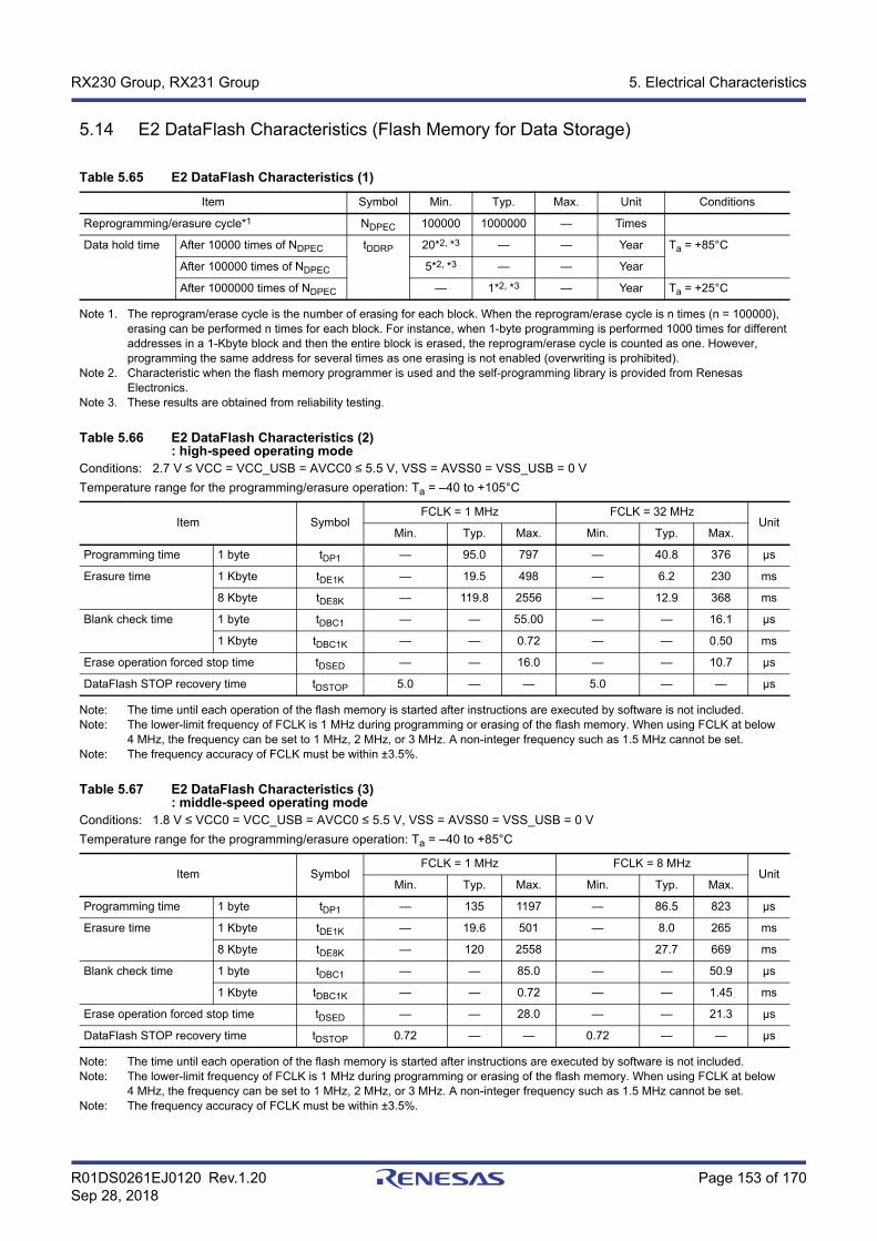
R01DS0261EJ0120 Rev.1.20 Page 153 of 170Sep 28, 2018
RX230 Group, RX231 Group 5. Electrical Characteristics
5.14 E2 DataFlash Characteristics (Flash Memory for Data Storage)
Note 1. The reprogram/erase cycle is the number of erasing for each block. When the reprogram/erase cycle is n times (n = 100000), erasing can be performed n times for each block. For instance, when 1-byte programming is performed 1000 times for different addresses in a 1-Kbyte block and then the entire block is erased, the reprogram/erase cycle is counted as one. However, programming the same address for several times as one erasing is not enabled (overwriting is prohibited).
Note 2. Characteristic when the flash memory programmer is used and the self-programming library is provided from Renesas Electronics.
Note 3. These results are obtained from reliability testing.
Note: The time until each operation of the flash memory is started after instructions are executed by software is not included.Note: The lower-limit frequency of FCLK is 1 MHz during programming or erasing of the flash memory. When using FCLK at below
4 MHz, the frequency can be set to 1 MHz, 2 MHz, or 3 MHz. A non-integer frequency such as 1.5 MHz cannot be set.Note: The frequency accuracy of FCLK must be within ±3.5%.
Table 5.65 E2 DataFlash Characteristics (1)
Item Symbol Min. Typ. Max. Unit Conditions
Reprogramming/erasure cycle*1 NDPEC 100000 1000000 — Times
Data hold time After 10000 times of NDPEC tDDRP 20*2, *3 — — Year Ta = +85°C
After 100000 times of NDPEC 5*2, *3 — — Year
After 1000000 times of NDPEC — 1*2, *3 — Year Ta = +25°C
Table 5.66 E2 DataFlash Characteristics (2): high-speed operating mode
Conditions: 2.7 V ≤ VCC = VCC_USB = AVCC0 ≤ 5.5 V, VSS = AVSS0 = VSS_USB = 0 VTemperature range for the programming/erasure operation: Ta = –40 to +105°C
Item SymbolFCLK = 1 MHz FCLK = 32 MHz
UnitMin. Typ. Max. Min. Typ. Max.
Programming time 1 byte tDP1 — 95.0 797 — 40.8 376 μs
Erasure time 1 Kbyte tDE1K — 19.5 498 — 6.2 230 ms
8 Kbyte tDE8K — 119.8 2556 — 12.9 368 ms
Blank check time 1 byte tDBC1 — — 55.00 — — 16.1 μs
1 Kbyte tDBC1K — — 0.72 — — 0.50 ms
Erase operation forced stop time tDSED — — 16.0 — — 10.7 μs
DataFlash STOP recovery time tDSTOP 5.0 — — 5.0 — — μs
Table 5.67 E2 DataFlash Characteristics (3): middle-speed operating mode
Conditions: 1.8 V ≤ VCC0 = VCC_USB = AVCC0 ≤ 5.5 V, VSS = AVSS0 = VSS_USB = 0 VTemperature range for the programming/erasure operation: Ta = –40 to +85°C
Item SymbolFCLK = 1 MHz FCLK = 8 MHz
UnitMin. Typ. Max. Min. Typ. Max.
Programming time 1 byte tDP1 — 135 1197 — 86.5 823 μs
Erasure time 1 Kbyte tDE1K — 19.6 501 — 8.0 265 ms
8 Kbyte tDE8K — 120 2558 27.7 669 ms
Blank check time 1 byte tDBC1 — — 85.0 — — 50.9 μs
1 Kbyte tDBC1K — — 0.72 — — 1.45 ms
Erase operation forced stop time tDSED — — 28.0 — — 21.3 μs
DataFlash STOP recovery time tDSTOP 0.72 — — 0.72 — — μs
R01DS0261EJ0120 Rev.1.20 Page 154 of 170Sep 28, 2018
RX230 Group, RX231 Group 5. Electrical Characteristics
5.15 Usage Notes
5.15.1 Connecting VCL Capacitor and Bypass CapacitorsThis MCU integrates an internal voltage-down circuit, which is used for lowering the power supply voltage in the internal MCU automatically to the optimum level. A 4.7-μF capacitor needs to be connected between this internal voltage-down power supply (VCL pin) and the VSS pin. Figure 5.80 to Figure 5.82 shows how to connect external capacitors. Place an external capacitor close to the pins. Do not apply the power supply voltage to the VCL pin.Insert a multilayer ceramic capacitor as a bypass capacitor between each pair of the power supply pins. Implement a bypass capacitor as closer to the MCU power supply pins as possible. Use a recommended value of 0.1 μF as the capacitance of the capacitors. For the capacitors related to crystal oscillation, see section 9, Clock Generation Circuit in the User’s Manual: Hardware. For the capacitors related to analog modules, also see section 43, 12-Bit A/D Converter (S12ADE) in the User’s Manual: Hardware.For notes on designing the printed circuit board, see the descriptions of the application note, the Hardware Design Guide (R01AN1411EJ). The latest version can be downloaded from the Renesas Electronics website.
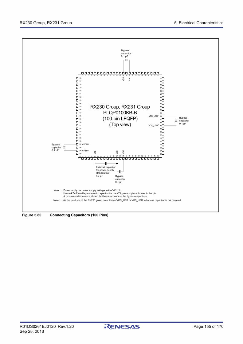
R01DS0261EJ0120 Rev.1.20 Page 155 of 170Sep 28, 2018
RX230 Group, RX231 Group 5. Electrical Characteristics
Figure 5.80 Connecting Capacitors (100 Pins)
Note: Do not apply the power supply voltage to the VCL pin.Use a 4.7-µF multilayer ceramic capacitor for the VCL pin and place it close to the pin.A recommended value is shown for the capacitance of the bypass capacitors.
External capacitor for power supply stabilization4.7 µF Bypass
capacitor0.1 µF
Bypass capacitor0.1 µF
Bypass capacitor0.1 µF
1 2 3 4 5 6 7 8 9 10 11 12 13 14 15 16 17 18 19 20 21 22 23 24 25
75 74 73 72 71 70 69 68 67 66 65 64 63 62 61 60 59 58 57 56 55 54 53 52 51
50
49
48
47
46
45
44
43
42
41
40
39
38
37
36
35
34
33
32
31
30
29
28
27
26
76
77
78
79
80
81
82
83
84
85
86
87
88
89
90
91
92
93
94
95
96
97
98
99
100
AVCC0
AVSS0
VSS_USB*1
VCC_USB*1VS
S
VCC
VCL
VSS
VCC
RX230 Group, RX231 GroupPLQP0100KB-B(100-pin LFQFP)
(Top view)
Bypass capacitor0.1 µF
Note 1. As the products of the RX230 group do not have VCC_USB or VSS_USB, a bypass capacitor is not required.

R01DS0261EJ0120 Rev.1.20 Page 156 of 170Sep 28, 2018
RX230 Group, RX231 Group 5. Electrical Characteristics
Figure 5.81 Connecting Capacitors (64 Pins)
Note: Do not apply the power supply voltage to the VCL pin.Use a 4.7-µF multilayer ceramic capacitor for the VCL pin and place it close to the pin.A recommended value is shown for the capacitance of the bypass capacitors.
External capacitor for power supply stabilization4.7 µF Bypass
capacitor0.1 µF
Bypass capacitor0.1 µF
Bypass capacitor0.1 µF
48 47 46 45 44 43 42 41 40 39 38 37 36 35 34 33
32
31
30
29
28
27
26
25
24
23
22
21
20
19
18
17
1 2 3 4 5 6 7 8 9 10 11 12 13 14 15 16
54
55
51
49
50
52
53
56
57
58
59
60
61
63
64
62
RX230 Group, RX231 Group
PLQP0064KB-C(64-pin LFQFP)
(Top view)AVCC0
AVSS0
VSS
VCC
VSS_USB*1
VCC_USB*1
VCL
VSS
VCC
Bypass capacitor0.1 µF
Note 1. As the products of the RX230 group do not have VCC_USB or VSS_USB, a bypass capacitor is not required.
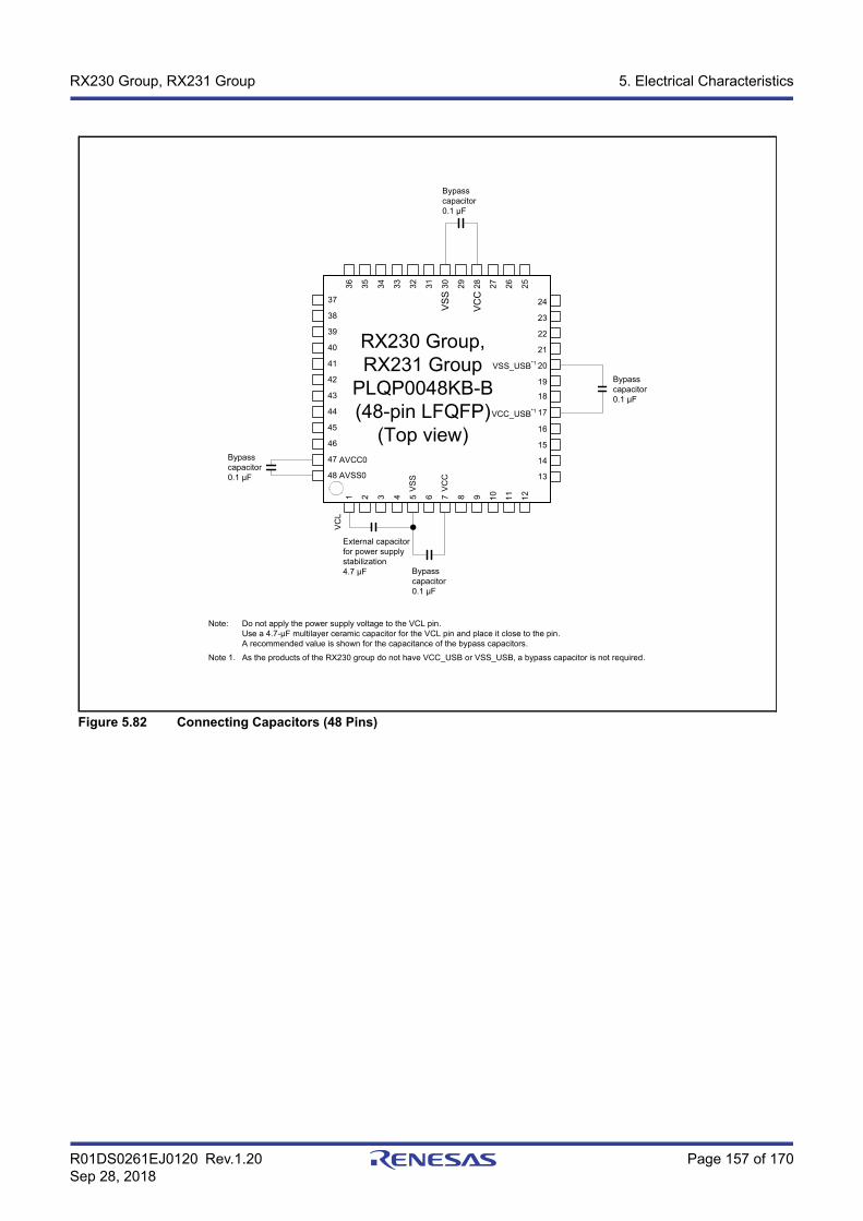
R01DS0261EJ0120 Rev.1.20 Page 157 of 170Sep 28, 2018
RX230 Group, RX231 Group 5. Electrical Characteristics
Figure 5.82 Connecting Capacitors (48 Pins)
36 35 34 33 32 31 30 29 28 27 26 25
24
23
22
21
20
19
1 2 3 4 5 6 7 8 9 10 11 12
38
39
37
40
41
42
43
44
45
47
48
46
RX230 Group, RX231 Group
PLQP0048KB-B(48-pin LFQFP)
(Top view)AVCC0
AVSS0
VSS
VCC
VSS_USB*1
VCC_USB*1VS
S
VCC
18
17
16
15
14
13
Note: Do not apply the power supply voltage to the VCL pin.Use a 4.7-µF multilayer ceramic capacitor for the VCL pin and place it close to the pin.A recommended value is shown for the capacitance of the bypass capacitors.
Bypass capacitor0.1 µF
External capacitor for power supply stabilization4.7 µF Bypass
capacitor0.1 µF
Bypass capacitor0.1 µF
Bypass capacitor0.1 µF
VCL
Note 1. As the products of the RX230 group do not have VCC_USB or VSS_USB, a bypass capacitor is not required.
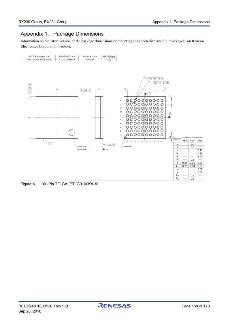
R01DS0261EJ0120 Rev.1.20 Page 158 of 170Sep 28, 2018
RX230 Group, RX231 Group Appendix 1. Package Dimensions
Appendix 1. Package DimensionsInformation on the latest version of the package dimensions or mountings has been displayed in “Packages” on Renesas Electronics Corporation website.
Figure A 100 -Pin TFLGA (PTLG0100KA-A)
e
e
A
B
C
D
E
F
G
H
J
K
1 2 3 4 5 6 7 8 9 10
B
A
S
y S
Index mark Index mark
(Laser mark)
x4
v
Aw S
Bw
S
D
E
ZD
ZE
A
S ABMφ ×
S ABMφ ×
φb1
φb
0.15
1.05
0.08
0.08
ReferenceSymbol
Dimension in Millimeters
Min Nom Max
D
E
v
ZD
b1
b
5.5
5.5
0.5
0.5
A
0.5e
w
x
y
ZE
0.20
0.250.21 0.29
0.340.29 0.39
P-TFLGA100-5.5x5.5-0.50 0.1g
MASS[Typ.]
100F0MPTLG0100KA-A
RENESAS CodeJEITA Package Code Previous Code
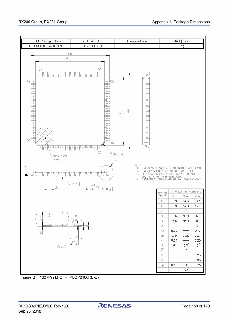
R01DS0261EJ0120 Rev.1.20 Page 159 of 170Sep 28, 2018
RX230 Group, RX231 Group Appendix 1. Package Dimensions
Figure B 100 -Pin LFQFP (PLQP0100KB-B)

R01DS0261EJ0120 Rev.1.20 Page 160 of 170Sep 28, 2018
RX230 Group, RX231 Group Appendix 1. Package Dimensions
Figure C 64 -Pin WFLGA (PWLG0064KA-A)
64-PIN PLASTIC FLGA (5x5)
E
w
5.00 0.10
0.20
y
0.20
0.08
y1
ZD 0.75
0.05x
D 5.00 0.10
A 0.69 0.07
b 0.25 0.04
P64FC-50-AN5
ZE 0.75
S
BSw
Sy
y1
e 0.50
INDEX MARK
w S A ZD
ZE
A
b
S
A
B
e
x S
8
7
6
5
4
3
2
1
BCDEFGH A
C
D
C DDETAIL DETAIL EDETAIL
M60x A B
ITEM DIMENSIONS
(UNIT:mm)
3.90
3.90
b
0.34 0.030.55
0.70 0.030.55 0.04
0.70 0.030.55 0.04
0.75 0.750.55 0.55
R0.17 0.015 R0.17 0.015R0.125 0.02 R0.125 0.02
R0.275 0.02
R0.35 0.0150.75
0.55 0.040.70 0.03
0.550.75
0.55 0.040.70 0.03
(LAND PAD)
(APERTURE OFSOLDER RESIST)
E
E
D
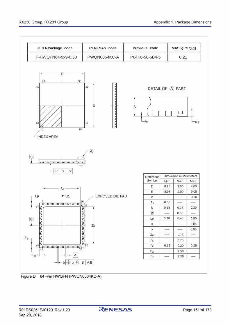
R01DS0261EJ0120 Rev.1.20 Page 161 of 170Sep 28, 2018
RX230 Group, RX231 Group Appendix 1. Package Dimensions
Figure D 64 -Pin HWQFN (PWQN0064KC-A)
Sy
e
Lp
Sxb A BM
A
D
E
4832
33
1617
1
64
A
S
B
A
D
E
49
DETAIL OF A PART
EXPOSED DIE PAD
JEITA Package code RENESAS code Previous code MASS(TYP.)[g]
P-HWQFN64-9x9-0.50 PWQN0064KC-A P64K8-50-6B4-5 0.21
161
17
3249
64
INDEX AREA
2
2
D
A
Lp
0.20
7.50
0.40
9.009.00
7.50
ReferenceSymbol Min Nom Max
Dimension in Millimeters
0.30
0.30 0.50
b 0.18
x
A 0.80
y 0.05
0.00
0.25e
Z
Z
c
DE
1
D
E
2
2
2
E
0.50
0.05
0.75
0.75
0.15 0.25
A1 c 2
9.058.959.058.95
Z
Z
D
E
3348

R01DS0261EJ0120 Rev.1.20 Page 162 of 170Sep 28, 2018
RX230 Group, RX231 Group Appendix 1. Package Dimensions
Figure E 64 -Pin LFQFP (PLQP0064KB-C)
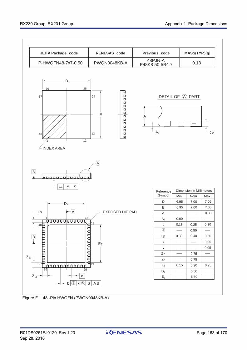
R01DS0261EJ0120 Rev.1.20 Page 163 of 170Sep 28, 2018
RX230 Group, RX231 Group Appendix 1. Package Dimensions
Figure F 48 -Pin HWQFN (PWQN0048KB-A)
Sy
e
Lp
Sxb A BM
A
D
E
36
24
25
12
13
1
48
A
S
B
A
D
E
37
DETAIL OF A PART
EXPOSED DIE PAD
JEITA Package code RENESAS code Previous code MASS(TYP.)[g]
P-HWQFN48-7x7-0.50 PWQN0048KB-A 48PJN-A 0.13
121
13
2437
48
INDEX AREA
2
2
D
A
Lp
0.20
5.50
0.40
7.007.00
5.50
ReferenceSymbol Min Nom Max
Dimension in Millimeters
0.30
0.30 0.50
b 0.18
x
A 0.80
y 0.05
0.00
0.25e
Z
Z
c
DE
1
D
E
2
2
2
E
0.50
0.05
0.75
0.75
0.15 0.25
A1 c 2
7.056.957.056.95
Z
Z
D
E
2536
P48K8-50-5B4-7
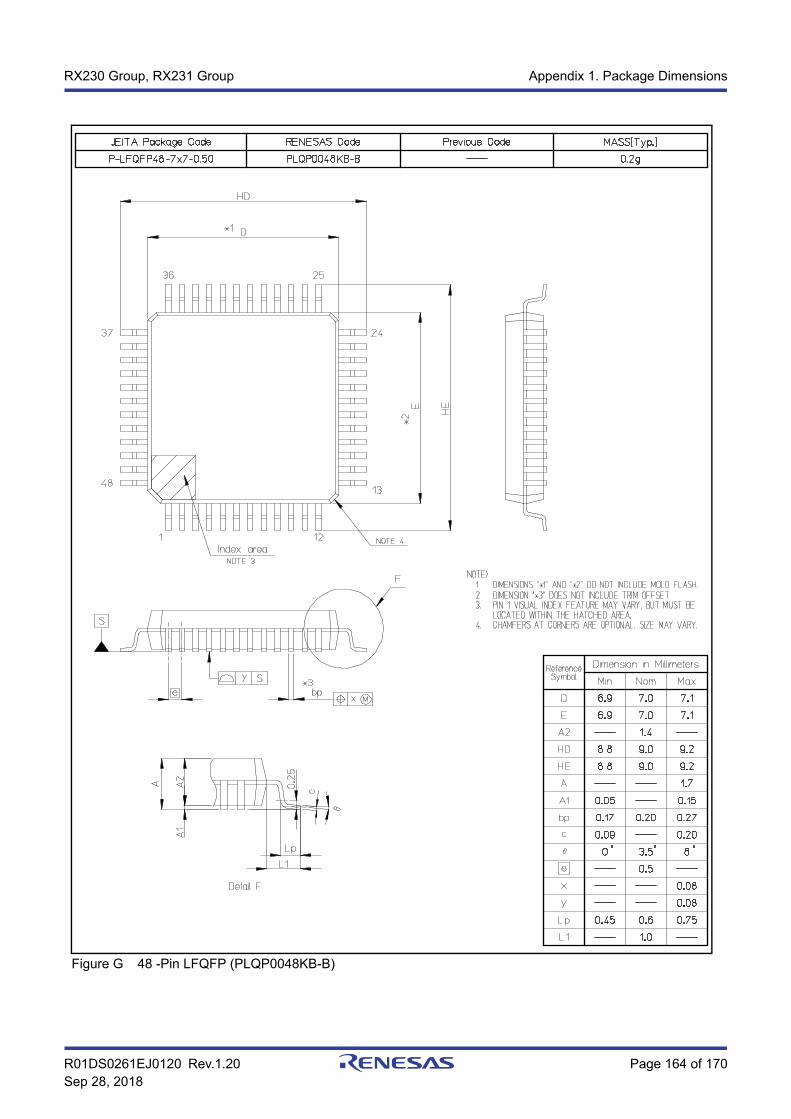
R01DS0261EJ0120 Rev.1.20 Page 164 of 170Sep 28, 2018
RX230 Group, RX231 Group Appendix 1. Package Dimensions
Figure G 48 -Pin LFQFP (PLQP0048KB-B)

R01DS0261EJ0120 Rev.1.20 Page 165 of 170Sep 28, 2018
RX230 Group, RX231 Group REVISION HISTORY
Classifications- Items with Technical Update document number: Changes according to the corresponding issued Technical Update- Items without Technical Update document number: Minor changes that do not require Technical Update to be issued
REVISION HISTORY RX230 Group, RX231 Group Datasheet
Rev. DateDescription
ClassificationPage Summary
1.00 Jun 24, 2015 — First edition, issued1.10 Oct 30, 2015 1. Overview
3 Table 1.1 Outline of Specifications (2/4), changed5 Table 1.1 Outline of Specifications (4/4): SD Host Interface (SDHIa) added6 Table 1.2 Comparison of Functions for Different Packages:
RX230 Group added3. Address Space
39 Figure 3.1 Memory Map in Each Operating Mode, changed4. I/O Registers
67 Table 4.1 List of I/O Registers (Address Order) (25 / 42), changed TN-RX*-A139A/E83 Table 4.1 List of I/O Registers (Address Order) (41 / 42), changed
5. Electrical Characteristics85 Table 5.1 Absolute Maximum Ratings, changed TN-RX*-A137A/E86 Table 5.2 Recommended Operating Voltage Conditions, changed87 Table 5.3 DC Characteristics (1), changed TN-RX*-A137A/E88 Table 5.4 DC Characteristics (2), changed88 Table 5.5 DC Characteristics (3), changed89 Table 5.7 DC Characteristics (5), changed91 Figure 5.1 Voltage Dependency in High-Speed Operating Mode (Reference
Data), changed92 Figure 5.2 Voltage Dependency in Middle-Speed Operating Mode
(Reference Data), changed93 Figure 5.3 Voltage Dependency in Low-Speed Operating Mode (Reference
Data), changedTN-RX*-A137A/E
94 Table 5.8 DC Characteristics (6), changedFigure 5.4 Voltage Dependency in Software Standby Mode (Reference Data), changed
95 Figure 5.5 Temperature Dependency in Software Standby Mode (Reference Data), changed
96 Figure 5.6 Temperature Dependency of RTC Operation with VCC Off (Reference Data), changedTable 5.10 DC Characteristics (8): Conditions changed
97 Table 5.11 DC Characteristics (9), changed TN-RX*-A137A/E99 Table 5.16 Permissible Output Currents (1), changed TN-RX*-A137A/E100 Table 5.17 Permissible Output Currents (2), changed101 Table 5.18 Output Values of Voltage (1), changed101 Table 5.19 Output Values of Voltage (2), changed TN-RX*-A137A/E101 Table 5.20 Output Values of Voltage (3), changed TN-RX*-A137A/E105 Figure 5.13 VOH/VOL and IOH/IOL Voltage Characteristics at Ta = 25°C
When High-Drive Output is Selected (Reference Data), changedTN-RX*-A137A/E
108 Figure 5.18 VOL and IOL Voltage Characteristics of RIIC Output Pin at Ta = 25°C (Reference Data)
TN-RX*-A137A/E
110 Table 5.21 Operating Frequency Value (High-Speed Operating Mode) and Table 5.22 Operating Frequency Value (Middle-Speed Operating Mode), changed
TN-RX*-A137A/E
112 Table 5.26 Clock Timing, changed TN-RX*-A137A/E116 Table 5.27 Reset Timing, changed131 Table 5.41 Timing of On-Chip Peripheral Modules (4): Note changed132 Table 5.43 Timing of On-Chip Peripheral Modules (6), changed138 Figure 5.61 SSI Transmission/Reception Timing (SSICP.SCKP=0), changed TN-RX*-A137A/E139 Figure 5.62 SSI Transmission/Reception Timing (SSICP.SCKP=1), changed TN-RX*-A137A/E142 Figure 5.66 VREFH0 Voltage Range vs. AVCC0, changed
REVISION HISTORY
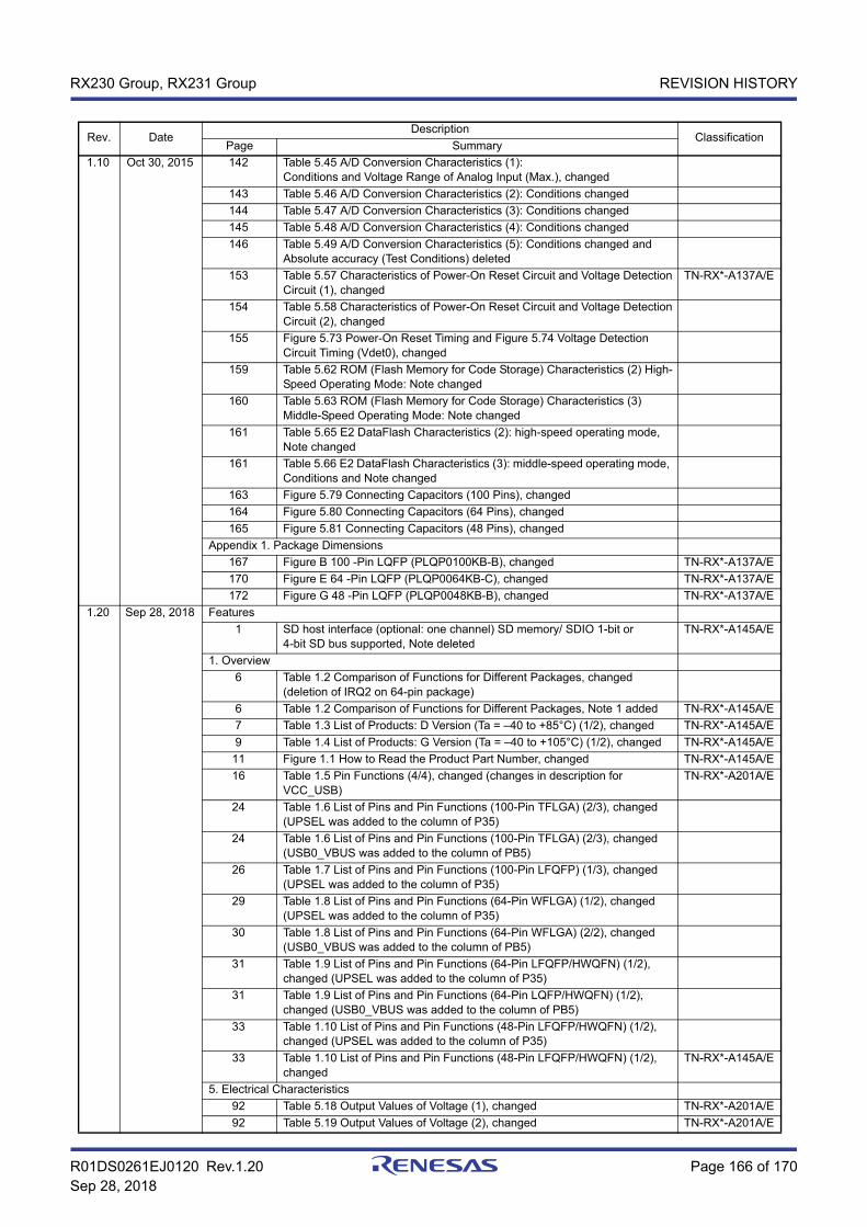
R01DS0261EJ0120 Rev.1.20 Page 166 of 170Sep 28, 2018
RX230 Group, RX231 Group REVISION HISTORY
1.10 Oct 30, 2015 142 Table 5.45 A/D Conversion Characteristics (1): Conditions and Voltage Range of Analog Input (Max.), changed
143 Table 5.46 A/D Conversion Characteristics (2): Conditions changed144 Table 5.47 A/D Conversion Characteristics (3): Conditions changed145 Table 5.48 A/D Conversion Characteristics (4): Conditions changed146 Table 5.49 A/D Conversion Characteristics (5): Conditions changed and
Absolute accuracy (Test Conditions) deleted153 Table 5.57 Characteristics of Power-On Reset Circuit and Voltage Detection
Circuit (1), changedTN-RX*-A137A/E
154 Table 5.58 Characteristics of Power-On Reset Circuit and Voltage Detection Circuit (2), changed
155 Figure 5.73 Power-On Reset Timing and Figure 5.74 Voltage Detection Circuit Timing (Vdet0), changed
159 Table 5.62 ROM (Flash Memory for Code Storage) Characteristics (2) High-Speed Operating Mode: Note changed
160 Table 5.63 ROM (Flash Memory for Code Storage) Characteristics (3) Middle-Speed Operating Mode: Note changed
161 Table 5.65 E2 DataFlash Characteristics (2): high-speed operating mode, Note changed
161 Table 5.66 E2 DataFlash Characteristics (3): middle-speed operating mode, Conditions and Note changed
163 Figure 5.79 Connecting Capacitors (100 Pins), changed164 Figure 5.80 Connecting Capacitors (64 Pins), changed165 Figure 5.81 Connecting Capacitors (48 Pins), changed
Appendix 1. Package Dimensions167 Figure B 100 -Pin LQFP (PLQP0100KB-B), changed TN-RX*-A137A/E170 Figure E 64 -Pin LQFP (PLQP0064KB-C), changed TN-RX*-A137A/E172 Figure G 48 -Pin LQFP (PLQP0048KB-B), changed TN-RX*-A137A/E
1.20 Sep 28, 2018 Features1 SD host interface (optional: one channel) SD memory/ SDIO 1-bit or
4-bit SD bus supported, Note deletedTN-RX*-A145A/E
1. Overview6 Table 1.2 Comparison of Functions for Different Packages, changed
(deletion of IRQ2 on 64-pin package)6 Table 1.2 Comparison of Functions for Different Packages, Note 1 added TN-RX*-A145A/E7 Table 1.3 List of Products: D Version (Ta = –40 to +85°C) (1/2), changed TN-RX*-A145A/E9 Table 1.4 List of Products: G Version (Ta = –40 to +105°C) (1/2), changed TN-RX*-A145A/E11 Figure 1.1 How to Read the Product Part Number, changed TN-RX*-A145A/E16 Table 1.5 Pin Functions (4/4), changed (changes in description for
VCC_USB)TN-RX*-A201A/E
24 Table 1.6 List of Pins and Pin Functions (100-Pin TFLGA) (2/3), changed (UPSEL was added to the column of P35)
24 Table 1.6 List of Pins and Pin Functions (100-Pin TFLGA) (2/3), changed (USB0_VBUS was added to the column of PB5)
26 Table 1.7 List of Pins and Pin Functions (100-Pin LFQFP) (1/3), changed (UPSEL was added to the column of P35)
29 Table 1.8 List of Pins and Pin Functions (64-Pin WFLGA) (1/2), changed (UPSEL was added to the column of P35)
30 Table 1.8 List of Pins and Pin Functions (64-Pin WFLGA) (2/2), changed (USB0_VBUS was added to the column of PB5)
31 Table 1.9 List of Pins and Pin Functions (64-Pin LFQFP/HWQFN) (1/2), changed (UPSEL was added to the column of P35)
31 Table 1.9 List of Pins and Pin Functions (64-Pin LQFP/HWQFN) (1/2), changed (USB0_VBUS was added to the column of PB5)
33 Table 1.10 List of Pins and Pin Functions (48-Pin LFQFP/HWQFN) (1/2), changed (UPSEL was added to the column of P35)
33 Table 1.10 List of Pins and Pin Functions (48-Pin LFQFP/HWQFN) (1/2), changed
TN-RX*-A145A/E
5. Electrical Characteristics92 Table 5.18 Output Values of Voltage (1), changed TN-RX*-A201A/E92 Table 5.19 Output Values of Voltage (2), changed TN-RX*-A201A/E
Rev. DateDescription
ClassificationPage Summary
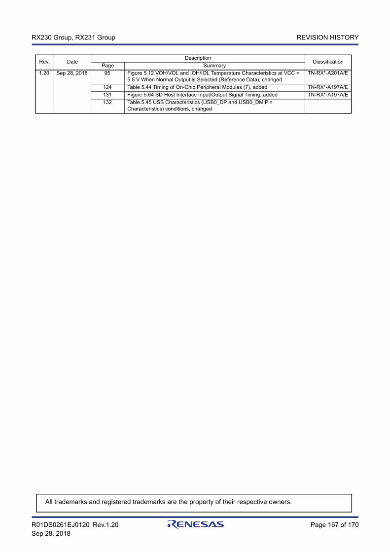
R01DS0261EJ0120 Rev.1.20 Page 167 of 170Sep 28, 2018
RX230 Group, RX231 Group REVISION HISTORY
1.20 Sep 28, 2018 95 Figure 5.12 VOH/VOL and IOH/IOL Temperature Characteristics at VCC = 5.5 V When Normal Output is Selected (Reference Data), changed
TN-RX*-A201A/E
124 Table 5.44 Timing of On-Chip Peripheral Modules (7), added TN-RX*-A197A/E131 Figure 5.64 SD Host Interface Input/Output Signal Timing, added TN-RX*-A197A/E132 Table 5.45 USB Characteristics (USB0_DP and USB0_DM Pin
Characteristics) conditions, changed
Rev. DateDescription
ClassificationPage Summary
All trademarks and registered trademarks are the property of their respective owners.
NOTES FOR CMOS DEVICES
(1) VOLTAGE APPLICATION WAVEFORM AT INPUT PIN: Waveform distortion due to input noise or a
reflected wave may cause malfunction. If the input of the CMOS device stays in the area between VIL (MAX) and VIH (MIN) due to noise, etc., the device may malfunction. Take care to prevent chattering noise from entering the device when the input level is fixed, and also in the transition period when the input level passes through the area between VIL (MAX) and VIH (MIN).
(2) HANDLING OF UNUSED INPUT PINS: Unconnected CMOS device inputs can be cause of malfunction. If an input pin is unconnected, it is possible that an internal input level may be generated due to noise, etc., causing malfunction. CMOS devices behave differently than Bipolar or NMOS devices. Input levels of CMOS devices must be fixed high or low by using pull-up or pull-down circuitry. Each unused pin should be connected to VDD or GND via a resistor if there is a possibility that it will be an output pin. All handling related to unused pins must be judged separately for each device and according to related specifications governing the device.
(3) PRECAUTION AGAINST ESD: A strong electric field, when exposed to a MOS device, can cause destruction of the gate oxide and ultimately degrade the device operation. Steps must be taken to stop generation of static electricity as much as possible, and quickly dissipate it when it has occurred. Environmental control must be adequate. When it is dry, a humidifier should be used. It is recommended to avoid using insulators that easily build up static electricity. Semiconductor devices must be stored and transported in an anti-static container, static shielding bag or conductive material. All test and measurement tools including work benches and floors should be grounded. The operator should be grounded using a wrist strap. Semiconductor devices must not be touched with bare hands. Similar precautions need to be taken for PW boards with mounted semiconductor devices.
(4) STATUS BEFORE INITIALIZATION: Power-on does not necessarily define the initial status of a MOS device. Immediately after the power source is turned ON, devices with reset functions have not yet been initialized. Hence, power-on does not guarantee output pin levels, I/O settings or contents of registers. A device is not initialized until the reset signal is received. A reset operation must be executed immediately after power-on for devices with reset functions.
(5) POWER ON/OFF SEQUENCE: In the case of a device that uses different power supplies for the internal operation and external interface, as a rule, switch on the external power supply after switching on the internal power supply. When switching the power supply off, as a rule, switch off the external power supply and then the internal power supply. Use of the reverse power on/off sequences may result in the application of an overvoltage to the internal elements of the device, causing malfunction and degradation of internal elements due to the passage of an abnormal current. The correct power on/off sequence must be judged separately for each device and according to related specifications governing the device.
(6) INPUT OF SIGNAL DURING POWER OFF STATE : Do not input signals or an I/O pull-up power supply while the device is not powered. The current injection that results from input of such a signal or I/O pull-up power supply may cause malfunction and the abnormal current that passes in the device at this time may cause degradation of internal elements. Input of signals during the power off state must be judged separately for each device and according to related specifications governing the device.
General Precautions in the Handling of Microprocessing Unit and Microcontroller Unit Products The following usage notes are applicable to all Microprocessing unit and Microcontroller unit products from Renesas. For detailed usage notes on the products covered by this document, refer to the relevant sections of the document as well as any technical updates that have been issued for the products.
1. Handling of Unused Pins Handle unused pins in accordance with the directions given under Handling of Unused Pins in the manual. ¾ The input pins of CMOS products are generally in the high-impedance state. In operation with an
unused pin in the open-circuit state, extra electromagnetic noise is induced in the vicinity of LSI, an associated shoot-through current flows internally, and malfunctions occur due to the false recognition of the pin state as an input signal become possible. Unused pins should be handled as described under Handling of Unused Pins in the manual.
2. Processing at Power-on The state of the product is undefined at the moment when power is supplied. ¾ The states of internal circuits in the LSI are indeterminate and the states of register settings and
pins are undefined at the moment when power is supplied. In a finished product where the reset signal is applied to the external reset pin, the states of pins are not guaranteed from the moment when power is supplied until the reset process is completed. In a similar way, the states of pins in a product that is reset by an on-chip power-on reset function are not guaranteed from the moment when power is supplied until the power reaches the level at which resetting has been specified.
3. Prohibition of Access to Reserved Addresses Access to reserved addresses is prohibited. ¾ The reserved addresses are provided for the possible future expansion of functions. Do not access
these addresses; the correct operation of LSI is not guaranteed if they are accessed. 4. Clock Signals
After applying a reset, only release the reset line after the operating clock signal has become stable. When switching the clock signal during program execution, wait until the target clock signal has stabilized. ¾ When the clock signal is generated with an external resonator (or from an external oscillator)
during a reset, ensure that the reset line is only released after full stabilization of the clock signal. Moreover, when switching to a clock signal produced with an external resonator (or by an external oscillator) while program execution is in progress, wait until the target clock signal is stable.
5. Differences between Products Before changing from one product to another, i.e. to a product with a different part number, confirm that the change will not lead to problems. ¾ The characteristics of Microprocessing unit or Microcontroller unit products in the same group but
having a different part number may differ in terms of the internal memory capacity, layout pattern, and other factors, which can affect the ranges of electrical characteristics, such as characteristic values, operating margins, immunity to noise, and amount of radiated noise. When changing to a product with a different part number, implement a system-evaluation test for the given product.
http://www.renesas.comRefer to "http://www.renesas.com/" for the latest and detailed information.
Renesas Electronics CorporationTOYOSU FORESIA, 3-2-24 Toyosu, Koto-ku, Tokyo 135-0061, JapanRenesas Electronics America Inc.1001 Murphy Ranch Road, Milpitas, CA 95035, U.S.A.Tel: +1-408-432-8888, Fax: +1-408-434-5351Renesas Electronics Canada Limited9251 Yonge Street, Suite 8309 Richmond Hill, Ontario Canada L4C 9T3Tel: +1-905-237-2004Renesas Electronics Europe LimitedDukes Meadow, Millboard Road, Bourne End, Buckinghamshire, SL8 5FH, U.KTel: +44-1628-651-700Renesas Electronics Europe GmbHArcadiastrasse 10, 40472 Düsseldorf, Germany Tel: +49-211-6503-0, Fax: +49-211-6503-1327Renesas Electronics (China) Co., Ltd.Room 1709 Quantum Plaza, No.27 ZhichunLu, Haidian District, Beijing, 100191 P. R. ChinaTel: +86-10-8235-1155, Fax: +86-10-8235-7679Renesas Electronics (Shanghai) Co., Ltd.Unit 301, Tower A, Central Towers, 555 Langao Road, Putuo District, Shanghai, 200333 P. R. China Tel: +86-21-2226-0888, Fax: +86-21-2226-0999Renesas Electronics Hong Kong LimitedUnit 1601-1611, 16/F., Tower 2, Grand Century Place, 193 Prince Edward Road West, Mongkok, Kowloon, Hong KongTel: +852-2265-6688, Fax: +852 2886-9022Renesas Electronics Taiwan Co., Ltd.13F, No. 363, Fu Shing North Road, Taipei 10543, TaiwanTel: +886-2-8175-9600, Fax: +886 2-8175-9670Renesas Electronics Singapore Pte. Ltd.80 Bendemeer Road, Unit #06-02 Hyflux Innovation Centre, Singapore 339949Tel: +65-6213-0200, Fax: +65-6213-0300Renesas Electronics Malaysia Sdn.Bhd.Unit 1207, Block B, Menara Amcorp, Amcorp Trade Centre, No. 18, Jln Persiaran Barat, 46050 Petaling Jaya, Selangor Darul Ehsan, MalaysiaTel: +60-3-7955-9390, Fax: +60-3-7955-9510Renesas Electronics India Pvt. Ltd.No.777C, 100 Feet Road, HAL 2nd Stage, Indiranagar, Bangalore 560 038, IndiaTel: +91-80-67208700, Fax: +91-80-67208777Renesas Electronics Korea Co., Ltd.17F, KAMCO Yangjae Tower, 262, Gangnam-daero, Gangnam-gu, Seoul, 06265 KoreaTel: +82-2-558-3737, Fax: +82-2-558-5338
SALES OFFICES
© 2018 Renesas Electronics Corporation. All rights reserved.Colophon 7.2
(Rev.4.0-1 November 2017)
Notice1. Descriptions of circuits, software and other related information in this document are provided only to illustrate the operation of semiconductor products and application examples. You are fully responsible for
the incorporation or any other use of the circuits, software, and information in the design of your product or system. Renesas Electronics disclaims any and all liability for any losses and damages incurred by
you or third parties arising from the use of these circuits, software, or information.
2. Renesas Electronics hereby expressly disclaims any warranties against and liability for infringement or any other claims involving patents, copyrights, or other intellectual property rights of third parties, by or
arising from the use of Renesas Electronics products or technical information described in this document, including but not limited to, the product data, drawings, charts, programs, algorithms, and application
examples.
3. No license, express, implied or otherwise, is granted hereby under any patents, copyrights or other intellectual property rights of Renesas Electronics or others.
4. You shall not alter, modify, copy, or reverse engineer any Renesas Electronics product, whether in whole or in part. Renesas Electronics disclaims any and all liability for any losses or damages incurred by
you or third parties arising from such alteration, modification, copying or reverse engineering.
5. Renesas Electronics products are classified according to the following two quality grades: “Standard” and “High Quality”. The intended applications for each Renesas Electronics product depends on the
product’s quality grade, as indicated below.
"Standard": Computers; office equipment; communications equipment; test and measurement equipment; audio and visual equipment; home electronic appliances; machine tools; personal electronic
equipment; industrial robots; etc.
"High Quality": Transportation equipment (automobiles, trains, ships, etc.); traffic control (traffic lights); large-scale communication equipment; key financial terminal systems; safety control equipment; etc.
Unless expressly designated as a high reliability product or a product for harsh environments in a Renesas Electronics data sheet or other Renesas Electronics document, Renesas Electronics products are
not intended or authorized for use in products or systems that may pose a direct threat to human life or bodily injury (artificial life support devices or systems; surgical implantations; etc.), or may cause
serious property damage (space system; undersea repeaters; nuclear power control systems; aircraft control systems; key plant systems; military equipment; etc.). Renesas Electronics disclaims any and all
liability for any damages or losses incurred by you or any third parties arising from the use of any Renesas Electronics product that is inconsistent with any Renesas Electronics data sheet, user’s manual or
other Renesas Electronics document.
6. When using Renesas Electronics products, refer to the latest product information (data sheets, user’s manuals, application notes, “General Notes for Handling and Using Semiconductor Devices” in the
reliability handbook, etc.), and ensure that usage conditions are within the ranges specified by Renesas Electronics with respect to maximum ratings, operating power supply voltage range, heat dissipation
characteristics, installation, etc. Renesas Electronics disclaims any and all liability for any malfunctions, failure or accident arising out of the use of Renesas Electronics products outside of such specified
ranges.
7. Although Renesas Electronics endeavors to improve the quality and reliability of Renesas Electronics products, semiconductor products have specific characteristics, such as the occurrence of failure at a
certain rate and malfunctions under certain use conditions. Unless designated as a high reliability product or a product for harsh environments in a Renesas Electronics data sheet or other Renesas
Electronics document, Renesas Electronics products are not subject to radiation resistance design. You are responsible for implementing safety measures to guard against the possibility of bodily injury, injury
or damage caused by fire, and/or danger to the public in the event of a failure or malfunction of Renesas Electronics products, such as safety design for hardware and software, including but not limited to
redundancy, fire control and malfunction prevention, appropriate treatment for aging degradation or any other appropriate measures. Because the evaluation of microcomputer software alone is very difficult
and impractical, you are responsible for evaluating the safety of the final products or systems manufactured by you.
8. Please contact a Renesas Electronics sales office for details as to environmental matters such as the environmental compatibility of each Renesas Electronics product. You are responsible for carefully and
sufficiently investigating applicable laws and regulations that regulate the inclusion or use of controlled substances, including without limitation, the EU RoHS Directive, and using Renesas Electronics
products in compliance with all these applicable laws and regulations. Renesas Electronics disclaims any and all liability for damages or losses occurring as a result of your noncompliance with applicable
laws and regulations.
9. Renesas Electronics products and technologies shall not be used for or incorporated into any products or systems whose manufacture, use, or sale is prohibited under any applicable domestic or foreign laws
or regulations. You shall comply with any applicable export control laws and regulations promulgated and administered by the governments of any countries asserting jurisdiction over the parties or
transactions.
10. It is the responsibility of the buyer or distributor of Renesas Electronics products, or any other party who distributes, disposes of, or otherwise sells or transfers the product to a third party, to notify such third
party in advance of the contents and conditions set forth in this document.
11. This document shall not be reprinted, reproduced or duplicated in any form, in whole or in part, without prior written consent of Renesas Electronics.
12. Please contact a Renesas Electronics sales office if you have any questions regarding the information contained in this document or Renesas Electronics products.
(Note 1) “Renesas Electronics” as used in this document means Renesas Electronics Corporation and also includes its directly or indirectly controlled subsidiaries.
(Note 2) “Renesas Electronics product(s)” means any product developed or manufactured by or for Renesas Electronics.
Related Documents