APPLICATION NOTE R01AN1819EJ0400 Rev.4.00 Page 1 of 59 Mar.14.22 RX Family DTC Module Using Firmware Integration Technology Introduction This application note describes the Data Transfer Controller (DTC) module which uses Firmware Integration Technology (FIT). This module uses DTC to control data transfer process using DTC software module. In this document, this module is referred to as the DTC FIT module. Target Devices • RX110 Group, RX111 Group, RX113 Group, RX130 Group, RX13T Group, RX140 Group • RX230 Group, RX231 Group, RX23T Group, RX24T Group, RX24U Group • RX23W Group • RX23E-A Group • RX64M Group, RX65N Group, RX651 Group, RX66T Group, RX66N Group, RX671 Group • RX71M Group • RX72T Group • RX72M Group, RX72N Group When using this application note with other Renesas MCUs, careful evaluation is recommended after making modifications to comply with the alternate MCU. Target Compilers • Renesas Electronics C/C++ Compiler Package for RX Family • GCC for Renesas RX • IAR C/C++ Compiler for Renesas RX (RX13T not supported) For details of the confirmed operation contents of each compiler, refer to “6.1 Confirmed Operation Environment".

Welcome message from author
This document is posted to help you gain knowledge. Please leave a comment to let me know what you think about it! Share it to your friends and learn new things together.
Transcript
APPLICATION NOTE
R01AN1819EJ0400 Rev.4.00 Page 1 of 59 Mar.14.22
RX Family DTC Module Using Firmware Integration Technology Introduction This application note describes the Data Transfer Controller (DTC) module which uses Firmware Integration Technology (FIT). This module uses DTC to control data transfer process using DTC software module. In this document, this module is referred to as the DTC FIT module.
Target Devices • RX110 Group, RX111 Group, RX113 Group, RX130 Group, RX13T Group, RX140 Group • RX230 Group, RX231 Group, RX23T Group, RX24T Group, RX24U Group • RX23W Group • RX23E-A Group • RX64M Group, RX65N Group, RX651 Group, RX66T Group, RX66N Group, RX671 Group • RX71M Group • RX72T Group • RX72M Group, RX72N Group When using this application note with other Renesas MCUs, careful evaluation is recommended after making modifications to comply with the alternate MCU.
Target Compilers • Renesas Electronics C/C++ Compiler Package for RX Family • GCC for Renesas RX • IAR C/C++ Compiler for Renesas RX (RX13T not supported) For details of the confirmed operation contents of each compiler, refer to “6.1 Confirmed Operation Environment".
RX Family DTC Module Using Firmware Integration Technology
R01AN1819EJ0400 Rev.4.00 Page 2 of 59 Mar.14.22
Contents
1. Overview ................................................................................................................................. 4 1.1 DTC FIT Module ...................................................................................................................................... 4 1.2 Overview of DTC FIT Module .................................................................................................................. 4 1.3 Using the FIT DTC module ...................................................................................................................... 6 1.3.1 Using FIT DTC module in C++ project .................................................................................................. 6 1.4 API Overview ........................................................................................................................................... 6 1.5 DTC IP Version ........................................................................................................................................ 7
2. API Information ........................................................................................................................ 8 2.1 Hardware Requirements ......................................................................................................................... 8 2.2 Software Requirements ........................................................................................................................... 8 2.3 Limitations ............................................................................................................................................... 8 2.3.1 RAM Location Limitations ...................................................................................................................... 8 2.4 Supported Toolchain ............................................................................................................................... 8 2.5 Interrupt Vector ........................................................................................................................................ 8 2.6 Header Files ............................................................................................................................................ 9 2.7 Integer Types ........................................................................................................................................... 9 2.8 Configuration Overview ......................................................................................................................... 10 2.9 Code Size .............................................................................................................................................. 11 2.10 Parameters ............................................................................................................................................ 15 2.10.1 r_dtc_rx_if.h ......................................................................................................................................... 15 2.10.2 r_dtc_rx_target_if.h ............................................................................................................................. 16 2.11 Return Values ........................................................................................................................................ 17 2.12 Callback function ................................................................................................................................... 17 2.13 Adding the FIT Module to Your Project ................................................................................................. 18 2.14 “for”, “while” and “do while” statements ................................................................................................. 19
3. API Functions ........................................................................................................................ 20 R_DTC_Open() ................................................................................................................................................ 20 R_DTC_Close() ............................................................................................................................................... 21 R_DTC_Create() .............................................................................................................................................. 23 R_DTC_CreateSeq() ....................................................................................................................................... 31 R_DTC_Control() ............................................................................................................................................. 38 R_DTC_GetVersion() ...................................................................................................................................... 43
4. Pin Setting ............................................................................................................................. 43
5. Demo Projects ....................................................................................................................... 44 5.1 dtc_demo_rskrx231, dtc_demo_rskrx231_gcc ..................................................................................... 44 5.2 dtc_demo_rskrx65n_2m, dtc_demo_rskrx65n_2m_gcc ....................................................................... 44 5.3 dtc_demo_rskrx130, dtc_demo_rskrx130_gcc ..................................................................................... 44
RX Family DTC Module Using Firmware Integration Technology
R01AN1819EJ0400 Rev.4.00 Page 3 of 59 Mar.14.22
5.4 dtc_demo_rskrx72m, dtc_demo_rskrx72m_gcc ................................................................................... 44 5.5 dtc_demo_rskrx671, dtc_demo_rskrx671_gcc ..................................................................................... 44 5.6 Adding a Demo to a Workspace ............................................................................................................ 44 5.7 Downloading Demo Projects ................................................................................................................. 44
6. Appendices ............................................................................................................................ 45 6.1 Confirmed Operation Environment ........................................................................................................ 45 6.2 Troubleshooting ..................................................................................................................................... 54
7. Reference Documents ........................................................................................................... 55
Related Technical Updates ........................................................................................................... 55
Revision History ............................................................................................................................ 56
RX Family DTC Module Using Firmware Integration Technology
R01AN1819EJ0400 Rev.4.00 Page 4 of 59 Mar.14.22
1. Overview 1.1 DTC FIT Module The DTC FIT module can be used by being implemented in a project as an API. See section 2.13, Adding the FIT Module to Your Project for details on methods to implement this FIT module into a project.
1.2 Overview of DTC FIT Module The DTC FIT module supports 3 transfer modes:
• Normal transfer mode • Repeat transfer mode • Block transfer mode
Each mode can enable Chain transfer and Sequence transfer functionality or not. For additional details, see the “Data Transfer Controller” section of the User’s Manual: Hardware.
The DTC is activated by interrupt requests from interrupt sources. The user should create transfer information corresponding to each activation source or many consecutive information elements in the case of chain transfers. Transfer information consists of a start address for source and destination and, configuration information controlling how the DTC will transfer the data. When the DTC in activated, it will read the corresponding Transfer information and start the transfer.
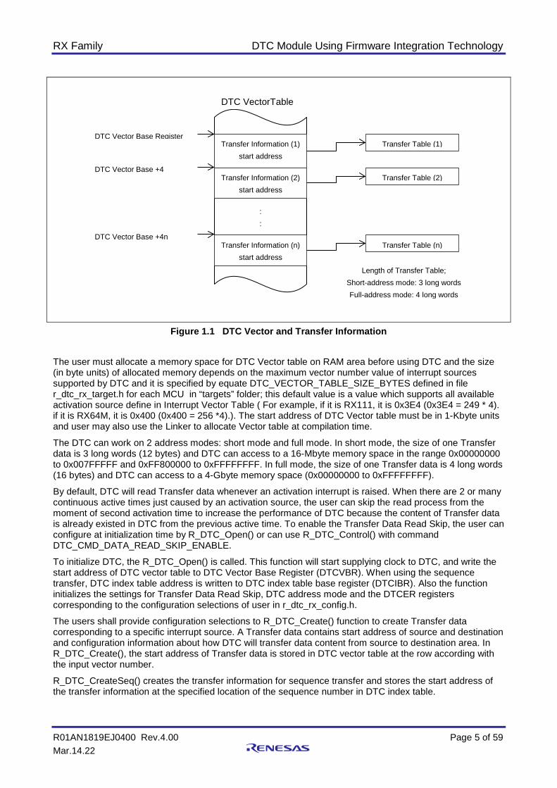
DTC reads start address of a Transfer data that belongs to a specified interrupt source in DTC Vector table. This Vector table is an array of 4 byte addresses and start address of Transfer data (n) that belong to interrupt source with vector number (n) will be stored at the row of table (element of array) having index (4 * n).
RX Family DTC Module Using Firmware Integration Technology
R01AN1819EJ0400 Rev.4.00 Page 5 of 59 Mar.14.22
Figure 1.1 DTC Vector and Transfer Information
The user must allocate a memory space for DTC Vector table on RAM area before using DTC and the size (in byte units) of allocated memory depends on the maximum vector number value of interrupt sources supported by DTC and it is specified by equate DTC_VECTOR_TABLE_SIZE_BYTES defined in file r_dtc_rx_target.h for each MCU in “targets” folder; this default value is a value which supports all available activation source define in Interrupt Vector Table ( For example, if it is RX111, it is 0x3E4 (0x3E4 = 249 * 4). if it is RX64M, it is 0x400 (0x400 = 256 *4).). The start address of DTC Vector table must be in 1-Kbyte units and user may also use the Linker to allocate Vector table at compilation time.
The DTC can work on 2 address modes: short mode and full mode. In short mode, the size of one Transfer data is 3 long words (12 bytes) and DTC can access to a 16-Mbyte memory space in the range 0x00000000 to 0x007FFFFF and 0xFF800000 to 0xFFFFFFFF. In full mode, the size of one Transfer data is 4 long words (16 bytes) and DTC can access to a 4-Gbyte memory space (0x00000000 to 0xFFFFFFFF).
By default, DTC will read Transfer data whenever an activation interrupt is raised. When there are 2 or many continuous active times just caused by an activation source, the user can skip the read process from the moment of second activation time to increase the performance of DTC because the content of Transfer data is already existed in DTC from the previous active time. To enable the Transfer Data Read Skip, the user can configure at initialization time by R_DTC_Open() or can use R_DTC_Control() with command DTC_CMD_DATA_READ_SKIP_ENABLE.
To initialize DTC, the R_DTC_Open() is called. This function will start supplying clock to DTC, and write the start address of DTC vector table to DTC Vector Base Register (DTCVBR). When using the sequence transfer, DTC index table address is written to DTC index table base register (DTCIBR). Also the function initializes the settings for Transfer Data Read Skip, DTC address mode and the DTCER registers corresponding to the configuration selections of user in r_dtc_rx_config.h.
The users shall provide configuration selections to R_DTC_Create() function to create Transfer data corresponding to a specific interrupt source. A Transfer data contains start address of source and destination and configuration information about how DTC will transfer data content from source to destination area. In R_DTC_Create(), the start address of Transfer data is stored in DTC vector table at the row according with the input vector number.
R_DTC_CreateSeq() creates the transfer information for sequence transfer and stores the start address of the transfer information at the specified location of the sequence number in DTC index table.
: :
Transfer Information (1) start address
Transfer Information (2) start address
DTC Vector Base Register
DTC VectorTable
DTC Vector Base +4
Transfer Information (n) start address
DTC Vector Base +4n Transfer Table (n)
Transfer Table (1)
Transfer Table (2)
Length of Transfer Table; Short-address mode: 3 long words Full-address mode: 4 long words
RX Family DTC Module Using Firmware Integration Technology
R01AN1819EJ0400 Rev.4.00 Page 6 of 59 Mar.14.22
The R_DTC_Control() is used to select (or deselect) an interrupt as a DTC activation source, start or stop supplying clock to DTC, enable or disable Transfer Data Read Skip, abort the current chain transfer process, and enable or disable or abort the sequence transfer.
DTC is active when the activation source raises an interrupt. It will read the Transfer data corresponding to the vector number of activation interrupt to self-configure, and then transfer the data. Users can also use R_DTC_Control() to get the current status of DTC: whether DTC is in progress, the vector number of current active interrupt. The driver also support aborting the current Chain transfer process and sequence transfer process via R_DTC_Control() function.
Usage Conditions of DTC FIT Module The usage conditions of the module are as follows.
• The r_bsp default lock function must be used. • A single common bit must be used as the DMAC module stop setting bit and the DTC module stop setting
bit.
1.3 Using the FIT DTC module 1.3.1 Using FIT DTC module in C++ project For C++ project, add FIT DTC module interface header file within extern “C”{}: Extern “C” {
#include “r_smc_entry.h” #include “r_dtc_rx_if.h”
}
1.4 API Overview Table 1.1 lists the API functions included in this module.
Table 1.1 API Functions
Function Name Description R_DTC_Open() Initialization Processing R_DTC_Close() End Processing R_DTC_Create() Register and Activation Source Setting Processing R_DTC_CreateSeq() Register and Activation Source Setting Processing for sequence
transfer R_DTC_Control() Operation Setting Processing R_DTC_GetVersion() Version Information Acquisition Processing
RX Family DTC Module Using Firmware Integration Technology
R01AN1819EJ0400 Rev.4.00 Page 7 of 59 Mar.14.22
1.5 DTC IP Version Table 1.2 lists relations about the DTC IP Version and target device.
The argument specifications of R_DTC_Create() function and the R_DTC_CreateSeq() function variable for the difference in DTC IP version. Refer to 3, API Functions.
Table 1.2 Lists of DTC IP Version
DTC IP Version Target Device DTCa RX110 Group, RX111 Group, RX113 Group, RX130 Group
RX230 Group, RX231 Group, RX23T Group, RX23W Group, RX23E-A Group, RX24T Group, RX24U Group RX64M Group, RX66T Group RX71M Group, RX72T Group
DTCb RX65N Group, RX66N Group, RX72M Group, RX72N Group, RX13T Group, RX671 Group, RX140 Group
RX Family DTC Module Using Firmware Integration Technology
R01AN1819EJ0400 Rev.4.00 Page 8 of 59 Mar.14.22
2. API Information This FIT module has been confirmed to operate under the following conditions.
2.1 Hardware Requirements The MCU used must support the following functions:
DTC (DTCa or DTCb) ICU
2.2 Software Requirements This driver is dependent upon the following FIT module:
Renesas Board Support Package (r_bsp) v5.20 or higher
2.3 Limitations 2.3.1 RAM Location Limitations In FIT, if a value equivalent to NULL is set as the pointer argument of an API function, error might be returned due to parameter check. Therefore, do not pass a NULL equivalent value as pointer argument to an API function.
The NULL value is defined as 0 because of the library function specifications. Therefore, the above phenomenon would occur when the variable or function passed to the API function pointer argument is located at the start address of RAM (address 0x0). In this case, change the section settings or prepare a dummy variable at the top of the RAM so that the variable or function passed to the API function pointer argument is not located at address 0x0.
In the case of the CCRX project (e2 studio V7.5.0), the RAM start address is set as 0x4 to prevent the variable from being located at address 0x0. In the case of the GCC project (e2 studio V7.5.0) and IAR project (EWRX V4.12.1), the start address of RAM is 0x0, so the above measures are necessary.
The default settings of the section may be changed due to the IDE version upgrade. Please check the section settings when using the latest IDE.
2.4 Supported Toolchain This driver has been confirmed to work with the toolchain listed in 6.1, Confirmed Operation Environment.
2.5 Interrupt Vector The DTC interrupt is enabled by executing the R_DTC_Create() function or the R_DTC_CreateSeq() (with specified condition) (while the macro definition DTC is 1).
Table 2.1 lists the interrupt vector used in the DTC FIT Module.
RX Family DTC Module Using Firmware Integration Technology
R01AN1819EJ0400 Rev.4.00 Page 9 of 59 Mar.14.22
Table 2.1 DTC Interrupt vector
Interrupt timing struct member When data transfer a specified number of times finished, Interrupt occurs to CPU.
response_interrupt DTC_INTERRUPT_AFTER_ALL_COMPLETE
Every time data transfer, Interrupt occurs to CPU.
DTC_INTERRUPT_PER_SINGLE_TRANSFER
2.6 Header Files All API calls and their supporting interface definitions are located in r_dtc_rx_if.h.
r_dtc_rx_target.h file should be included by User’s application, when allocating a memory space for DTC Vector table on RAM area using DTC_VECTOR_TABLE_SIZE_BYTES definition.
2.7 Integer Types This project uses ANSI C99. These types are defined in stdint.h.
RX Family DTC Module Using Firmware Integration Technology
R01AN1819EJ0400 Rev.4.00 Page 10 of 59 Mar.14.22
2.8 Configuration Overview The configuration option settings of this module are located in r_dtc_rx_config.h. The option names and setting values are listed in the table below:
Configuration options in r_dtc_rx_config.h
DTC_CFG_PARAM_CHECKING_ENABLE Note: The default value is the value of BSP_CFG_PARAM_CHECKING_ENABLE in the r_bsp_config.h file.
SPECIFY WHETHER TO INCLUDE CODE FOR API PARAMETER CHECKING 0: Compiles out parameter checking. 1: Includes parameter checking. Default value is set to BSP_CFG_PARAM_CHECKING_ENABLE to re-use the system default setting.
DTC_CFG_DISABLE_ALL_ACT_SOURCE Note: The default value is “DTC_ENABLE”.
SPECIFY WHETHER THE DTCER REGISTERS WILL BE CLEARED IN R_DTC_OPEN() DTC_DISABLE: Do nothing. DTC_ENABLE: Clear all DTCER registers in R_DTC_Open().
DTC_CFG_SHORT_ADDRESS_MODE Note: The default value is “DTC_DISABLE”.
SPECIFY WHICH ADDRESS MODE IS SUPPORTED BY DTC DTC_DISABLE: Select the Full-address mode. DTC_ENABLE: Select the Short-address mode.
DTC_CFG_TRANSFER_DATA_READ_SKIP_EN Note: The default value is “DTC_ENABLE”.
SPECIFY WHETHER THE TRANSFER DATA READ SKIP IS ENABLED DTC_DISABLE: Disable Transfer Data Read Skip. DTC_ENABLE: Enable Transfer Data Read Skip.
DTC_CFG_USE_DMAC_FIT_MODULE Note: The default value is “DTC_ENABLE”.
SPECIFY WHETHER THE DMAC FIT MODULE IS USED WITH DTC FIT MODULE DTC_DISABLE: DMAC FIT module is not used with DTC FIT module. DTC_ENABLE: DMAC FIT module is used with DTC FIT module. When DMAC FIT module is not used and “DTC_ENABLE” is set, the compiling error will be generated.
DTC_CFG_USE_SEQUENCE_TRANSFER Note: The default value is “DTC_DISABLE”.
SPECIFY WHETHER THE SEQUENCE TRANSFER IS USED. DTC_DISABLE: SEQUENCE TRANSFER is not used. DTC_ENABLE: SEQUENCE TRANSFER is used. When defined as “DTC_ENABLE”, set DTC_CFG_SHORT_ADDRESS_MODE to “DTC_DISABLE”. When defined both this definition and DTC_CFG_SHORT_ADDRESS_MODE as “DTC_ENABLE”, the compiling error will be generated. When defined as “DTC_ENABLE” for the MCU not supporting sequence transfer, the compiling error will be generated as well.
RX Family DTC Module Using Firmware Integration Technology
R01AN1819EJ0400 Rev.4.00 Page 11 of 59 Mar.14.22
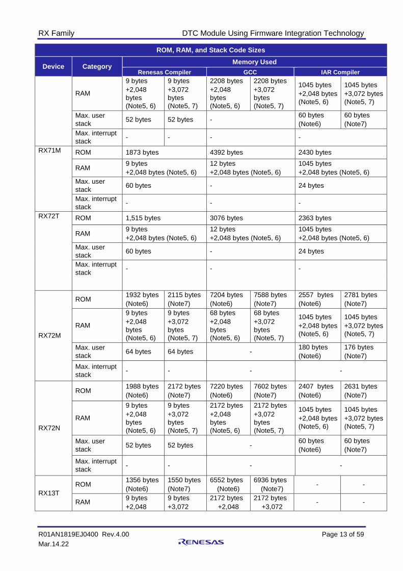
2.9 Code Size Typical code sizes associated with this module are listed below.
The ROM (code and constants) and RAM (global data) sizes are determined by the build-time configuration options described in 2.8, Configuration Overview. The table lists reference values when the C compiler’s compile options are set to their default values, as described in 2.4, Supported Toolchain. The compile option default values are optimization level: 2, optimization type: for size, and data endianness: little-endian. The code size varies depending on the C compiler version and compile options.
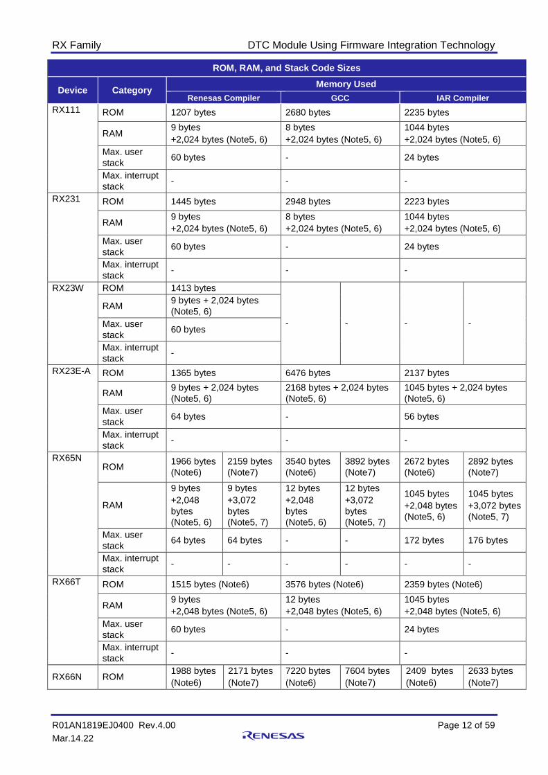
RX Family DTC Module Using Firmware Integration Technology
R01AN1819EJ0400 Rev.4.00 Page 12 of 59 Mar.14.22
ROM, RAM, and Stack Code Sizes
Device Category Memory Used Renesas Compiler GCC IAR Compiler
RX111 ROM 1207 bytes 2680 bytes 2235 bytes
RAM 9 bytes +2,024 bytes (Note5, 6)
8 bytes +2,024 bytes (Note5, 6)
1044 bytes +2,024 bytes (Note5, 6)
Max. user stack 60 bytes - 24 bytes
Max. interrupt stack - - -
RX231 ROM 1445 bytes 2948 bytes 2223 bytes
RAM 9 bytes +2,024 bytes (Note5, 6)
8 bytes +2,024 bytes (Note5, 6)
1044 bytes +2,024 bytes (Note5, 6)
Max. user stack 60 bytes - 24 bytes
Max. interrupt stack - - -
RX23W ROM 1413 bytes
- - - -
RAM 9 bytes + 2,024 bytes (Note5, 6)
Max. user stack 60 bytes
Max. interrupt stack -
RX23E-A ROM 1365 bytes 6476 bytes 2137 bytes
RAM 9 bytes + 2,024 bytes (Note5, 6)
2168 bytes + 2,024 bytes (Note5, 6)
1045 bytes + 2,024 bytes (Note5, 6)
Max. user stack 64 bytes - 56 bytes
Max. interrupt stack - - -
RX65N ROM 1966 bytes
(Note6) 2159 bytes (Note7)
3540 bytes (Note6)
3892 bytes (Note7)
2672 bytes (Note6)
2892 bytes (Note7)
RAM
9 bytes +2,048 bytes (Note5, 6)
9 bytes +3,072 bytes (Note5, 7)
12 bytes +2,048 bytes (Note5, 6)
12 bytes +3,072 bytes (Note5, 7)
1045 bytes +2,048 bytes (Note5, 6)
1045 bytes +3,072 bytes (Note5, 7)
Max. user stack 64 bytes 64 bytes - - 172 bytes 176 bytes
Max. interrupt stack - - - - - -
RX66T ROM 1515 bytes (Note6) 3576 bytes (Note6) 2359 bytes (Note6)
RAM 9 bytes +2,048 bytes (Note5, 6)
12 bytes +2,048 bytes (Note5, 6)
1045 bytes +2,048 bytes (Note5, 6)
Max. user stack 60 bytes - 24 bytes
Max. interrupt stack - - -
RX66N ROM 1988 bytes (Note6)
2171 bytes (Note7)
7220 bytes (Note6)
7604 bytes (Note7)
2409 bytes (Note6)
2633 bytes (Note7)
RX Family DTC Module Using Firmware Integration Technology
R01AN1819EJ0400 Rev.4.00 Page 13 of 59 Mar.14.22
ROM, RAM, and Stack Code Sizes
Device Category Memory Used Renesas Compiler GCC IAR Compiler
RAM
9 bytes +2,048 bytes (Note5, 6)
9 bytes +3,072 bytes (Note5, 7)
2208 bytes +2,048 bytes (Note5, 6)
2208 bytes +3,072 bytes (Note5, 7)
1045 bytes +2,048 bytes (Note5, 6)
1045 bytes +3,072 bytes (Note5, 7)
Max. user stack 52 bytes 52 bytes - 60 bytes
(Note6) 60 bytes (Note7)
Max. interrupt stack - - - -
RX71M ROM 1873 bytes 4392 bytes 2430 bytes
RAM 9 bytes +2,048 bytes (Note5, 6)
12 bytes +2,048 bytes (Note5, 6)
1045 bytes +2,048 bytes (Note5, 6)
Max. user stack 60 bytes - 24 bytes
Max. interrupt stack - - -
RX72T ROM 1,515 bytes 3076 bytes 2363 bytes
RAM 9 bytes +2,048 bytes (Note5, 6)
12 bytes +2,048 bytes (Note5, 6)
1045 bytes +2,048 bytes (Note5, 6)
Max. user stack 60 bytes - 24 bytes
Max. interrupt stack - - -
RX72M
ROM 1932 bytes (Note6)
2115 bytes (Note7)
7204 bytes (Note6)
7588 bytes (Note7)
2557 bytes (Note6)
2781 bytes (Note7)
RAM
9 bytes +2,048 bytes (Note5, 6)
9 bytes +3,072 bytes (Note5, 7)
68 bytes +2,048 bytes (Note5, 6)
68 bytes +3,072 bytes (Note5, 7)
1045 bytes +2,048 bytes (Note5, 6)
1045 bytes +3,072 bytes (Note5, 7)
Max. user stack 64 bytes 64 bytes - 180 bytes
(Note6) 176 bytes (Note7)
Max. interrupt stack - - - -
RX72N
ROM 1988 bytes (Note6)
2172 bytes (Note7)
7220 bytes (Note6)
7602 bytes (Note7)
2407 bytes (Note6)
2631 bytes (Note7)
RAM
9 bytes +2,048 bytes (Note5, 6)
9 bytes +3,072 bytes (Note5, 7)
2172 bytes +2,048 bytes (Note5, 6)
2172 bytes +3,072 bytes (Note5, 7)
1045 bytes +2,048 bytes (Note5, 6)
1045 bytes +3,072 bytes (Note5, 7)
Max. user stack 52 bytes 52 bytes - 60 bytes
(Note6) 60 bytes (Note7)
Max. interrupt stack - - - -
RX13T ROM 1356 bytes
(Note6) 1550 bytes (Note7)
6552 bytes (Note6)
6936 bytes (Note7) - -
RAM 9 bytes +2,048
9 bytes +3,072
2172 bytes +2,048
2172 bytes +3,072
- -
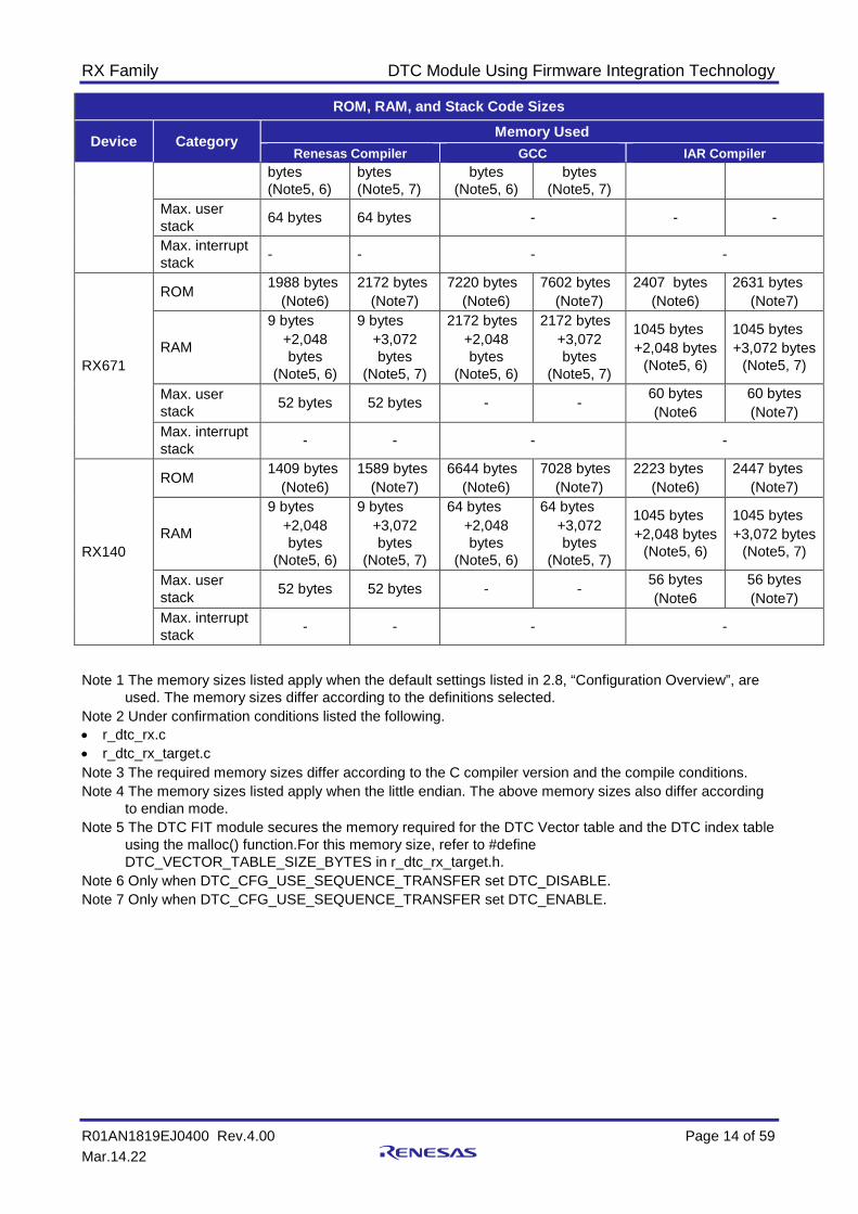
RX Family DTC Module Using Firmware Integration Technology
R01AN1819EJ0400 Rev.4.00 Page 14 of 59 Mar.14.22
ROM, RAM, and Stack Code Sizes
Device Category Memory Used Renesas Compiler GCC IAR Compiler
bytes (Note5, 6)
bytes (Note5, 7)
bytes (Note5, 6)
bytes (Note5, 7)
Max. user stack 64 bytes 64 bytes - - -
Max. interrupt stack - - - -
RX671
ROM 1988 bytes (Note6)
2172 bytes (Note7)
7220 bytes (Note6)
7602 bytes (Note7)
2407 bytes (Note6)
2631 bytes (Note7)
RAM
9 bytes +2,048 bytes
(Note5, 6)
9 bytes +3,072 bytes
(Note5, 7)
2172 bytes +2,048 bytes
(Note5, 6)
2172 bytes +3,072 bytes
(Note5, 7)
1045 bytes +2,048 bytes
(Note5, 6)
1045 bytes +3,072 bytes
(Note5, 7)
Max. user stack 52 bytes 52 bytes - - 60 bytes
(Note6 60 bytes (Note7)
Max. interrupt stack - - - -
RX140
ROM 1409 bytes (Note6)
1589 bytes (Note7)
6644 bytes (Note6)
7028 bytes (Note7)
2223 bytes (Note6)
2447 bytes (Note7)
RAM
9 bytes +2,048 bytes
(Note5, 6)
9 bytes +3,072 bytes
(Note5, 7)
64 bytes +2,048 bytes
(Note5, 6)
64 bytes +3,072 bytes
(Note5, 7)
1045 bytes +2,048 bytes
(Note5, 6)
1045 bytes +3,072 bytes
(Note5, 7)
Max. user stack 52 bytes 52 bytes - - 56 bytes
(Note6 56 bytes (Note7)
Max. interrupt stack - - - -
Note 1 The memory sizes listed apply when the default settings listed in 2.8, “Configuration Overview”, are used. The memory sizes differ according to the definitions selected.
Note 2 Under confirmation conditions listed the following. • r_dtc_rx.c • r_dtc_rx_target.c Note 3 The required memory sizes differ according to the C compiler version and the compile conditions. Note 4 The memory sizes listed apply when the little endian. The above memory sizes also differ according
to endian mode. Note 5 The DTC FIT module secures the memory required for the DTC Vector table and the DTC index table
using the malloc() function.For this memory size, refer to #define DTC_VECTOR_TABLE_SIZE_BYTES in r_dtc_rx_target.h.
Note 6 Only when DTC_CFG_USE_SEQUENCE_TRANSFER set DTC_DISABLE. Note 7 Only when DTC_CFG_USE_SEQUENCE_TRANSFER set DTC_ENABLE.
RX Family DTC Module Using Firmware Integration Technology
R01AN1819EJ0400 Rev.4.00 Page 15 of 59 Mar.14.22
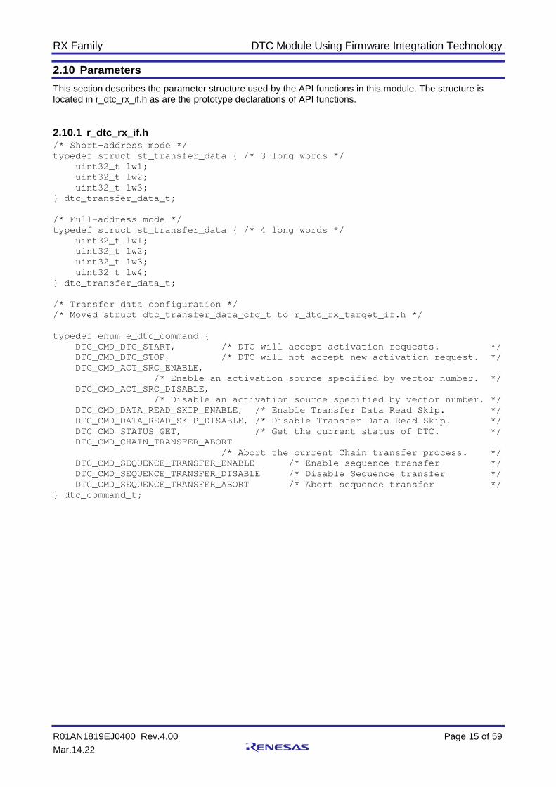
2.10 Parameters This section describes the parameter structure used by the API functions in this module. The structure is located in r_dtc_rx_if.h as are the prototype declarations of API functions.
2.10.1 r_dtc_rx_if.h /* Short-address mode */ typedef struct st_transfer_data { /* 3 long words */ uint32_t lw1; uint32_t lw2; uint32_t lw3; } dtc_transfer_data_t; /* Full-address mode */ typedef struct st_transfer_data { /* 4 long words */ uint32_t lw1; uint32_t lw2; uint32_t lw3; uint32_t lw4; } dtc_transfer_data_t; /* Transfer data configuration */ /* Moved struct dtc_transfer_data_cfg_t to r_dtc_rx_target_if.h */ typedef enum e_dtc_command { DTC_CMD_DTC_START, /* DTC will accept activation requests. */ DTC_CMD_DTC_STOP, /* DTC will not accept new activation request. */ DTC_CMD_ACT_SRC_ENABLE, /* Enable an activation source specified by vector number. */ DTC_CMD_ACT_SRC_DISABLE, /* Disable an activation source specified by vector number. */ DTC_CMD_DATA_READ_SKIP_ENABLE, /* Enable Transfer Data Read Skip. */ DTC_CMD_DATA_READ_SKIP_DISABLE, /* Disable Transfer Data Read Skip. */ DTC_CMD_STATUS_GET, /* Get the current status of DTC. */ DTC_CMD_CHAIN_TRANSFER_ABORT /* Abort the current Chain transfer process. */ DTC_CMD_SEQUENCE_TRANSFER_ENABLE /* Enable sequence transfer */ DTC_CMD_SEQUENCE_TRANSFER_DISABLE /* Disable Sequence transfer */ DTC_CMD_SEQUENCE_TRANSFER_ABORT /* Abort sequence transfer */ } dtc_command_t;
RX Family DTC Module Using Firmware Integration Technology
R01AN1819EJ0400 Rev.4.00 Page 16 of 59 Mar.14.22
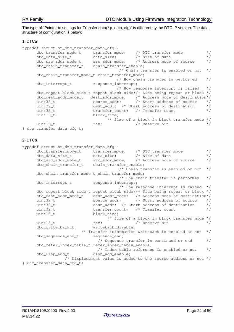
2.10.2 r_dtc_rx_target_if.h dtc_transfer_data_cfg_t has different definition according to DTC IP Version.
1. DTCa typedef struct st_dtc_transfer_data_cfg { dtc_transfer_mode_t transfer_mode; /* DTC transfer mode */ dtc_data_size_t data_size; /* Size of data */ dtc_src_addr_mode_t src_addr_mode; /* Address mode of source */ dtc_chain_transfer_t chain_transfer_enable; /* Chain transfer is enabled or not */ dtc_chain_transfer_mode_t chain_transfer_mode; /* How chain transfer is performed */ dtc_interrupt_t response_interrupt; /* How response interrupt is raised */ dtc_repeat_block_side_t repeat_block_side;/* Side being repeat or block */ dtc_dest_addr_mode_t dest_addr_mode; /* Address mode of destination*/ uint32_t source_addr; /* Start address of source */ uint32_t dest_addr; /* Start address of destination */ uint32_t transfer_count; /* Transfer count */ uint16_t block_size; /* Size of a block in block transfer mode */ uint16_t rsv; /* Reserve bit */ } dtc_transfer_data_cfg_t;
2. DTCb typedef struct st_dtc_transfer_data_cfg { dtc_transfer_mode_t transfer_mode; /* DTC transfer mode */ dtc_data_size_t data_size; /* Size of data */ dtc_src_addr_mode_t src_addr_mode; /* Address mode of source */ dtc_chain_transfer_t chain_transfer_enable; /* Chain transfer is enabled or not */ dtc_chain_transfer_mode_t chain_transfer_mode; /* How chain transfer is performed */ dtc_interrupt_t response_interrupt; /* How response interrupt is raised */ dtc_repeat_block_side_t repeat_block_side;/* Side being repeat or block */ dtc_dest_addr_mode_t dest_addr_mode; /* Address mode of destination*/ uint32_t source_addr; /* Start address of source */ uint32_t dest_addr; /* Start address of destination */ uint32_t transfer_count; /* Transfer count */ uint16_t block_size; /* Size of a block in block transfer mode */ uint16_t rsv; /* Reserve bit */ dtc_write_back_t writeback_disable; /* Transfer information writeback is enabled or not */ dtc_sequence_end_t sequence_end; /* Sequence transfer is continued or end */ dtc_refer_index_table_t refer_index_table_enable; /* Index table reference is enabled or not */ dtc_disp_add_t disp_add_enable; /* Displacement value is added to the source address or not */ } dtc_transfer_data_cfg_t;
RX Family DTC Module Using Firmware Integration Technology
R01AN1819EJ0400 Rev.4.00 Page 17 of 59 Mar.14.22
2.11 Return Values This section describes return values of API functions. This enumeration is located in r_dtc_rx_if.h as are the prototype declarations of API functions. typedef enum e_dtc_err /* DTC API error codes */ { DTC_SUCCESS_DMAC_BUSY = 0, /* One or some DMAC resources are locked by another process. */ DTC_SUCCESS, DTC_ERR_OPENED, /* DTC was initialized already. */ DTC_ERR_NOT_OPEN, /* DTC module is not initialized yet. */ DTC_ERR_INVALID_ARG, /* Arguments are invalid. */ DTC_ERR_INVALID_COMMAND, /* Command parameters are invalid. */ DTC_ERR_NULL_PTR, /* Argument pointers are NULL. */ DTC_ERR_BUSY /* The DTC resources are locked by another process. */ DTC_ERR_ACT /* Data transfer is in progress */ } dtc_err_t;
2.12 Callback function DTC FIT module don’t use callback function.
RX Family DTC Module Using Firmware Integration Technology
R01AN1819EJ0400 Rev.4.00 Page 18 of 59 Mar.14.22
2.13 Adding the FIT Module to Your Project This module must be added to each project in which it is used. Renesas recommends the method using the Smart Configurator described in (1) or (3) below. However, the Smart Configurator only supports some RX devices. Please use the methods of (2) or (4) for RX devices that are not supported by the Smart Configurator.
(1) Adding the FIT module to your project using the Smart Configurator in e2 studio By using the Smart Configurator in e2 studio, the FIT module is automatically added to your project. Refer to “Renesas e2 studio Smart Configurator User Guide (R20AN0451)” for details.
(2) Adding the FIT module to your project using the FIT Configurator in e2 studio By using the FIT Configurator in e2 studio, the FIT module is automatically added to your project. Refer to “Adding Firmware Integration Technology Modules to Projects (R01AN1723)” for details.
(3) Adding the FIT module to your project using the Smart Configurator in CS+ By using the Smart Configurator Standalone version in CS+, the FIT module is automatically added to your project. Refer to “Renesas e2 studio Smart Configurator User Guide (R20AN0451)” for details.
(4) Adding the FIT module to your project in CS+ In CS+, please manually add the FIT module to your project. Refer to “Adding Firmware Integration Technology Modules to CS+ Projects (R01AN1826)” for details.
RX Family DTC Module Using Firmware Integration Technology
R01AN1819EJ0400 Rev.4.00 Page 19 of 59 Mar.14.22
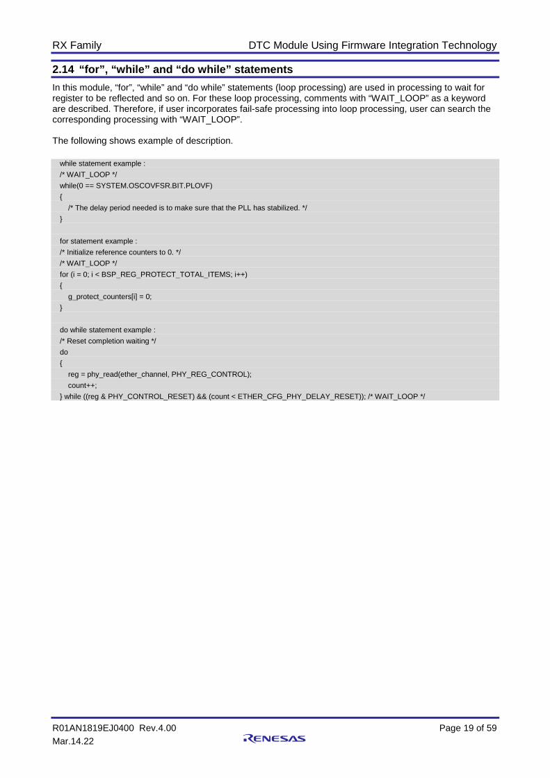
2.14 “for”, “while” and “do while” statements In this module, “for”, “while” and “do while” statements (loop processing) are used in processing to wait for register to be reflected and so on. For these loop processing, comments with “WAIT_LOOP” as a keyword are described. Therefore, if user incorporates fail-safe processing into loop processing, user can search the corresponding processing with “WAIT_LOOP”. The following shows example of description.
while statement example : /* WAIT_LOOP */ while(0 == SYSTEM.OSCOVFSR.BIT.PLOVF) { /* The delay period needed is to make sure that the PLL has stabilized. */ } for statement example : /* Initialize reference counters to 0. */ /* WAIT_LOOP */ for (i = 0; i < BSP_REG_PROTECT_TOTAL_ITEMS; i++) { g_protect_counters[i] = 0; } do while statement example : /* Reset completion waiting */ do { reg = phy_read(ether_channel, PHY_REG_CONTROL); count++; } while ((reg & PHY_CONTROL_RESET) && (count < ETHER_CFG_PHY_DELAY_RESET)); /* WAIT_LOOP */
RX Family DTC Module Using Firmware Integration Technology
R01AN1819EJ0400 Rev.4.00 Page 20 of 59 Mar.14.22
3. API Functions
R_DTC_Open() This function is run first when using the APIs of the DTC FIT module.
Format dtc_err_t R_DTC_Open ( void )
Parameters None.
Return Values [DTC_SUCCESS] /* Successful operation */ [DTC_ERR_OPENED] /* DTC has been initialized already. */ [DTC_ERR_BUSY] /* Resource has been locked by other process. */
Properties Prototype declarations are contained in r_dtc_rx_if.h.
Description Locks*1 the DTC and starts supplying clock to DTC, then initializes DTC vector table, address mode, Data Transfer Read Skip. When setting DTC_CFG_DISABLE_ALL_ACT_SOURCE to DTC_ENABLE in r_dtc_rx_config.h, all DTCER registers are cleared. When setting DTC_CFG_USE_SEQUENCE_TRANSFER to DTC_ENABLE, the area used in DTC index table is secured.
Note: 1. The DTC FIT module uses the r_bsp default lock function. As a result, the DTC is in the locked state after a successful end.
Example dtc_err_t ret; /* Call R_DTC_Open() */ ret = R_DTC_Open();
Special Notes: Set #define BSP_CFG_HEAP_BYTES in r_bsp_config.h to the value greater than #define DTC_VECTOR_TABLE_SIZE_BYTES in r_dtc_rx_target.h.
This is to secure the DTC Vector table area using the malloc() function in the DTC FIT module.
RX Family DTC Module Using Firmware Integration Technology
R01AN1819EJ0400 Rev.4.00 Page 21 of 59 Mar.14.22
R_DTC_Close() This function is used to release the resources of the DTC.
Format dtc_err_t R_DTC_Close ( void )
Parameters None.
Return Values [DTC_SUCCESS] /* Successful operation */ [DTC_SUCCESS_DMAC_BUSY] /* Successful operation.One or some DMAC
resources are locked. */
Properties Prototype declarations are contained in r_dtc_rx_if.h.
Description Unlocks*1 the DTC and disable all DTC activation source by clearing the DTC Activation Enable Register DTCERn; stop supplying clock to DTC and put it to Module stop state.
If in addition all DMAC channels have been unlocked, the function sets the DMAC and DTC to the module stop state.*2
Note: 1. The DTC FIT module uses the r_bsp default lock function. As a result, the DTC is in the unlocked state after a successful end.
2. Because a shared bit is used as both the DMAC module stop setting bit and the DTC module stop setting bit, the function confirms that all DMAC channels are unlocked before making the module stop setting. (For details, see the “Low Power Consumption” section in the User’s Manual: Hardware.
Change the processing method to match the combination of modules used, as shown below.
DMAC Control DTC Control Processing Method DMACA FIT module (lock function control function present, DTC lock state checking function present)
DTC FIT module (lock function control function present, DMAC lock state checking function present)
See case 1.
Other than the above See case 2.
RX Family DTC Module Using Firmware Integration Technology
R01AN1819EJ0400 Rev.4.00 Page 22 of 59 Mar.14.22
Case 1: Using the r_bsp Default Lock Function and Controlling the DMAC with the DMAC FIT Module*1
The function uses the r_bsp default lock function to confirm that all DMAC channels are unlocked and that the DTC is unlocked, then puts the DTC into the module stop state.
Note: 1. A necessary condition is that the DMAC FIT module has a module stop control function that confirms the locked state of the DTC.
Case 2: Control Other Than the Above The user must provide code to confirm that all DMAC channels are unlocked and that the DTC is unlocked (not in use). The DTC FIT module includes an empty function for this purpose.
If the r_bsp default lock function is not used, insert the program code for checking the locked/unlocked state of all the DMAC channels and the DTC after the line marked /* do something */ in the r_dtc_check_DMAC_locking_byUSER() function in the file r_dtc_rx_target.c.
Note that bool type shown below should be used for the return value of the r_dtc_check_DMAC_locking_byUSER() function.
Returns value of r_dtc_check_DMAC_locking_byUSER() [true] /* All DMAC channels are unlocked. */ [false] /* One or some DMAC channels are locked. */
Example dtc_err_t ret; ret = R_DTC_Close();
Special Notes: When controlling the DMAC without using the DMAC FIT module, make sure to monitor the usage of the DMAC and control locking and unlocking of the DMAC so that calling this function does not set the DMAC to the module stop state. Note that even if the DMAC has not been activated, it is necessary to keep it in the locked state when not making DMAC transfer settings.
RX Family DTC Module Using Firmware Integration Technology
R01AN1819EJ0400 Rev.4.00 Page 23 of 59 Mar.14.22
R_DTC_Create() This function is used to make DTC register settings and to specify the activation source.
Format dtc_err_t R_DTC_Create (
dtc_activation_source_t act_source,
dtc_transfer_data_t *p_transfer_data,
dtc_transfer_data_cfg_t *p_data_cfg,
uint32_t chain_transfer_nr
)
Parameters dtc_activation_source_t act_source Activation source. dtc_transfer_data_t *p_transfer_data Pointer to start address of Transfer data area on RAM. dtc_transfer_data_cfg_t *p_data_cfg Pointer to settings for Transfer data
In the case of DTCb, the setting to the following structure members is invalid. This function sets the following values.
p_data_cfg->writeback_disable = DTC_WRITEBACK_ENABLE; p_data_cfg->sequence_end = DTC_SEQUENCE_TRANSFER_CONTINUE; p_data_cfg->refer_index_table_enable = DTC_REFER_INDEX_TABLE_DISABLE; p_data_cfg->disp_add_enable = DTC_SRC_ADDR_DISP_ADD_DISABLE; uint32_t chain_transfer_nr Number of chain transfer
The number of Transfer data and corresponding configurations is (number of chain transfer + 1). Example: if chain_transfer_nr = 1, it means that there are 2 continuous Transfer data and 2 corresponding configurations and the first configuration enable the chain transfer.
The type definition of a Transfer data (* p_transfer_data) depends on the address mode and the details are shown as below and the users will use this data type to allocate memory for Transfer data exactly: #if (1 == DTC_CFG_SHORT_ADDRESS_MODE) /* Short address mode */ typedef struct st_transfer_data { /* 3 long words */ uint32_t lw1; uint32_t lw2; uint32_t lw3; } dtc_transfer_data_t; #else /* Full-address mode */ typedef struct st_transfer_data { /* 4 long words */ uint32_t lw1; uint32_t lw2; uint32_t lw3; uint32_t lw4; } dtc_transfer_data_t; #endif
RX Family DTC Module Using Firmware Integration Technology
R01AN1819EJ0400 Rev.4.00 Page 24 of 59 Mar.14.22
The type of “Pointer to settings for Transfer data(* p_data_cfg)” is different by the DTC IP version. The data structure of configuration is below: 1. DTCa typedef struct st_dtc_transfer_data_cfg { dtc_transfer_mode_t transfer_mode; /* DTC transfer mode */ dtc_data_size_t data_size; /* Size of data */ dtc_src_addr_mode_t src_addr_mode; /* Address mode of source */ dtc_chain_transfer_t chain_transfer_enable; /* Chain transfer is enabled or not */ dtc_chain_transfer_mode_t chain_transfer_mode; /* How chain transfer is performed */ dtc_interrupt_t response_interrupt; /* How response interrupt is raised */ dtc_repeat_block_side_t repeat_block_side;/* Side being repeat or block */ dtc_dest_addr_mode_t dest_addr_mode; /* Address mode of destination*/ uint32_t source_addr; /* Start address of source */ uint32_t dest_addr; /* Start address of destination */ uint32_t transfer_count; /* Transfer count */ uint16_t block_size; /* Size of a block in block transfer mode */ uint16_t rsv; /* Reserve bit */ } dtc_transfer_data_cfg_t;
2. DTCb typedef struct st_dtc_transfer_data_cfg { dtc_transfer_mode_t transfer_mode; /* DTC transfer mode */ dtc_data_size_t data_size; /* Size of data */ dtc_src_addr_mode_t src_addr_mode; /* Address mode of source */ dtc_chain_transfer_t chain_transfer_enable; /* Chain transfer is enabled or not */ dtc_chain_transfer_mode_t chain_transfer_mode; /* How chain transfer is performed */ dtc_interrupt_t response_interrupt; /* How response interrupt is raised */ dtc_repeat_block_side_t repeat_block_side;/* Side being repeat or block */ dtc_dest_addr_mode_t dest_addr_mode; /* Address mode of destination*/ uint32_t source_addr; /* Start address of source */ uint32_t dest_addr; /* Start address of destination */ uint32_t transfer_count; /* Transfer count */ uint16_t block_size; /* Size of a block in block transfer mode */ uint16_t rsv; /* Reserve bit */ dtc_write_back_t writeback_disable; /* Transfer information writeback is enabled or not */ dtc_sequence_end_t sequence_end; /* Sequence transfer is continued or end */ dtc_refer_index_table_t refer_index_table_enable; /* Index table reference is enabled or not */ dtc_disp_add_t disp_add_enable; /* Displacement value is added to the source address or not */ } dtc_transfer_data_cfg_t;
RX Family DTC Module Using Firmware Integration Technology
R01AN1819EJ0400 Rev.4.00 Page 25 of 59 Mar.14.22
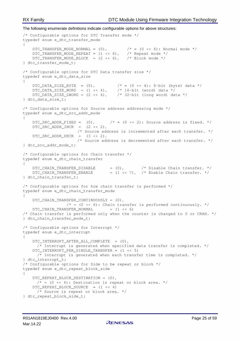
The following enumerate definitions indicate configurable options for above structures: /* Configurable options for DTC Transfer mode */ typedef enum e_dtc_transfer_mode { DTC_TRANSFER_MODE_NORMAL = (0), /* = (0 << 6): Normal mode */ DTC_TRANSFER_MODE_REPEAT = (1 << 6), /* Repeat mode */ DTC_TRANSFER_MODE_BLOCK = (2 << 6), /* Block mode */ } dtc_transfer_mode_t; /* Configurable options for DTC Data transfer size */ typedef enum e_dtc_data_size { DTC_DATA_SIZE_BYTE = (0), /* = (0 << 4): 8-bit (byte) data */ DTC_DATA_SIZE_WORD = (1 << 4), /* 16-bit (word) data */ DTC_DATA_SIZE_LWORD = (2 << 4), /* 32-bit (long word) data */ } dtc_data_size_t; /* Configurable options for Source address addressing mode */ typedef enum e_dtc_src_addr_mode { DTC_SRC_ADDR_FIXED = (0), /* = (0 << 2): Source address is fixed. */ DTC_SRC_ADDR_INCR = (2 << 2),
/* Source address is incremented after each transfer. */ DTC_SRC_ADDR_DECR = (3 << 2),
/* Source address is decremented after each transfer. */ } dtc_src_addr_mode_t; /* Configurable options for Chain transfer */ typedef enum e_dtc_chain_transfer { DTC_CHAIN_TRANSFER_DISABLE = (0), /* Disable Chain transfer. */ DTC_CHAIN_TRANSFER_ENABLE = (1 << 7), /* Enable Chain transfer. */ } dtc_chain_transfer_t; /* Configurable options for how chain transfer is performed */ typedef enum e_dtc_chain_transfer_mode { DTC_CHAIN_TRANSFER_CONTINUOUSLY = (0), /* = (0 << 6): Chain transfer is performed continuously. */ DTC_CHAIN_TRANSFER_NORMAL = (1 << 6) /* Chain transfer is performed only when the counter is changed to 0 or CRAH. */ } dtc_chain_transfer_mode_t; /* Configurable options for Interrupt */ typedef enum e_dtc_interrupt { DTC_INTERRUPT_AFTER_ALL_COMPLETE = (0),
/* Interrupt is generated when specified data transfer is completed. */ DTC_INTERRUPT_PER_SINGLE_TRANSFER = (1 << 5)
/* Interrupt is generated when each transfer time is completed. */ } dtc_interrupt_t; /* Configurable options for Side to be repeat or block */ typedef enum e_dtc_repeat_block_side { DTC_REPEAT_BLOCK_DESTINATION = (0),
/* = (0 << 4): Destination is repeat or block area. */ DTC_REPEAT_BLOCK_SOURCE = (1 << 4)
/* Source is repeat or block area. */ } dtc_repeat_block_side_t;
RX Family DTC Module Using Firmware Integration Technology
R01AN1819EJ0400 Rev.4.00 Page 26 of 59 Mar.14.22
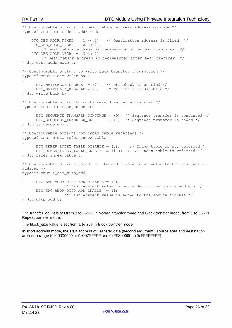
/* Configurable options for Destination address addressing mode */ typedef enum e_dtc_dest_addr_mode { DTC_DES_ADDR_FIXED = (1 << 2), /* Destination address is fixed. */ DTC_DES_ADDR_INCR = (2 << 2),
/* Destination address is incremented after each transfer. */ DTC_DES_ADDR_DECR = (3 << 2)
/* Destination address is decremented after each transfer. */ } dtc_dest_addr_mode_t; /* Configurable options to write back transfer information */ typedef enum e_dtc_write_back { DTC_WRITEBACK_ENABLE = (0), /* Writeback is enabled */ DTC_WRITEBACK_DISABLE = (1) /* Writeback is disabled */ } dtc_write_back_t; /* Configurable option to continue/end sequence transfer */ typedef enum e_dtc_sequence_end { DTC_SEQUENCE_TRANSFER_CONTINUE = (0), /* Sequence transfer is continued */ DTC_SEQUENCE_TRANSFER_END = (1) /* Sequence transfer is ended */ } dtc_sequence_end_t; /* Configurable options for index table reference */ typedef enum e_dtc_refer_index_table { DTC_REFER_INDEX_TABLE_DISABLE = (0), /* Index table is not referred */ DTC_REFER_INDEX_TABLE_ENABLE = (1 << 1) /* Index table is referred */ } dtc_refer_index_table_t; /* Configurable options to add/not to add Displacement value to the destination address */ typedef enum e_dtc_disp_add { DTC_SRC_ADDR_DISP_ADD_DISABLE = (0), /* Displacement value is not added to the source address */ DTC_SRC_ADDR_DISP_ADD_ENABLE = (1) /* Displacement value is added to the source address */ } dtc_disp_add_t; The transfer_count is set from 1 to 65536 in Normal transfer mode and Block transfer mode, from 1 to 256 in Repeat transfer mode.
The block_size value is set from 1 to 256 in Block transfer mode.
In short address mode, the start address of Transfer data (second argument), source area and destination area is in range (0x00000000 to 0x007FFFFF and 0xFF800000 to 0xFFFFFFFF).
RX Family DTC Module Using Firmware Integration Technology
R01AN1819EJ0400 Rev.4.00 Page 27 of 59 Mar.14.22
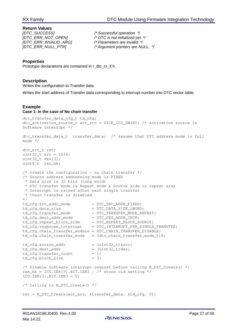
Return Values [DTC_SUCCESS] /* Successful operation */ [DTC_ERR_NOT_OPEN] /* DTC is not initialized yet. */ [DTC_ERR_INVALID_ARG] /* Parameters are invalid. */ [DTC_ERR_NULL_PTR] /* Argument pointers are NULL. */
Properties Prototype declarations are contained in r_dtc_rx_if.h.
Description Writes the configuration to Transfer data.
Writes the start address of Transfer data corresponding to interrupt number into DTC vector table.
Example Case 1: In the case of No chain transfer dtc_transfer_data_cfg_t td_cfg; dtc_activation_source_t act_src = DTCE_ICU_SWINT; /* activation source is Software Interrupt */ dtc_transfer_data_t transfer_data; /* assume that DTC address mode is full mode */ dtc_err_t ret; uint32_t src = 1234; uint32_t des[3]; uint8_t ien_bk; /* create the configuration – no chain transfer */ /* Source address addressing mode is FIXED * Data size is 32 bits (long word) * DTC transfer mode is Repeat mode & Source side is repeat area * Interrupt is raised after each single transfer * Chain transfer is disabled */ td_cfg.src_addr_mode = DTC_SRC_ADDR_FIXED; td_cfg.data_size = DTC_DATA_SIZE_LWORD; td_cfg.transfer_mode = DTC_TRANSFER_MODE_REPEAT; td_cfg.dest_addr_mode = DTC_DES_ADDR_INCR; td_cfg.repeat_block_side = DTC_REPEAT_BLOCK_SOURCE; td_cfg.response_interrupt = DTC_INTERRUPT_PER_SINGLE_TRANSFER; td_cfg.chain_transfer_enable = DTC_CHAIN_TRANSFER_DISABLE; td_cfg.chain_transfer_mode = (dtc_chain_transfer_mode_t)0; td_cfg.source_addr = (uint32_t)&src; td_cfg.dest_addr = (uint32_t)des; td_cfg.transfer_count = 1; td_cfg.block_size = 3; /* Disable Software interrupt request before calling R_DTC_Create() */ ien_bk = ICU.IER[3].BIT.IEN3 ; /* store old setting */ ICU.IER[3].BIT.IEN3 = 0; /* Calling to R_DTC_Create() */ ret = R_DTC_Create(act_src, &transfer_data, &td_cfg, 0);
RX Family DTC Module Using Firmware Integration Technology
R01AN1819EJ0400 Rev.4.00 Page 28 of 59 Mar.14.22
/* Restore the setting for Software interrupt request */ ICU.IER[3].BIT.IEN3 = ien_bk;
Case 2: In the case of ONE chain transfer dtc_transfer_data_cfg_t td_cfg[2]; /* need 2 configuration sets */ dtc_activation_source_t act_src = DTCE_ICU_SWINT;
/* activation source is Software Interrupt */ uint32_t transfer_data[8];
/* for 2 Transfer data; assume that DTC address mode is full mode */ dtc_err_t ret; uint32_t src = 1234; uint32_t des[3]; /* The destination for first Transfer data */ uint32_t des2[3]; /* The destination for second Transfer data */ uint8_t ien_bk; /* create the configuration 1 – support chain transfer */ /* Source address addressing mode is FIXED * Destination address addressing mode is INCREMENTED * Data size is 32 bits (long word) * DTC transfer mode is Normal mode * Interrupt is raised after each single transfer * Chain transfer is enabled * Chain transfer is performed after when transfer counter is set to 0 */ td_cfg[0].src_addr_mode = DTC_SRC_ADDR_FIXED; td_cfg[0].data_size = DTC_DATA_SIZE_LWORD; td_cfg[0].transfer_mode = DTC_TRANSFER_MODE_NORMAL; td_cfg[0].dest_addr_mode = DTC_DES_ADDR_INCR; td_cfg[0].repeat_block_side = DTC_REPEAT_BLOCK_SOURCE; td_cfg[0].response_interrupt = DTC_INTERRUPT_PER_SINGLE_TRANSFER; td_cfg[0].chain_transfer_enable = DTC_CHAIN_TRANSFER_ENABLE; td_cfg[0].chain_transfer_mode = DTC_CHAIN_TRANSFER_NORMAL; td_cfg[0].source_addr = (uint32_t)&src; td_cfg[0].dest_addr = (uint32_t)des; /* transfer from source to des 1 */ td_cfg[0].transfer_count = 1; td_cfg[0].block_size = 3; /* create the configuration 2 – no chain transfer */ /* Source address addressing mode is FIXED * Destination address addressing mode is INCREMENTED * Data size is 32 bits (long word) * DTC transfer mode is Normal mode * Interrupt is raised after each single transfer * Chain transfer is disabled */ td_cfg[1].src_addr_mode = DTC_SRC_ADDR_FIXED; td_cfg[1].data_size = DTC_DATA_SIZE_LWORD; td_cfg[1].transfer_mode = DTC_TRANSFER_MODE_NORMAL; td_cfg[1].dest_addr_mode = DTC_DES_ADDR_INCR; td_cfg[1].repeat_block_side = DTC_REPEAT_BLOCK_SOURCE; td_cfg[1].response_interrupt = DTC_INTERRUPT_PER_SINGLE_TRANSFER; td_cfg[1].chain_transfer_enable = DTC_CHAIN_TRANSFER_DISABLE; td_cfg[1].chain_transfer_mode = (dtc_chain_transfer_mode_t)0; td_cfg[1].source_addr = (uint32_t)&src; td_cfg[1].dest_addr = (uint32_t)des2; /* transfer from source to des 2*/ td_cfg[1].transfer_count = 1; td_cfg[1].block_size = 3; /* Disable Software interrupt request before calling R_DTC_Create() */
RX Family DTC Module Using Firmware Integration Technology
R01AN1819EJ0400 Rev.4.00 Page 29 of 59 Mar.14.22
ien_bk = ICU.IER[3].BIT.IEN3 ; /* store old setting */ ICU.IER[3].BIT.IEN3 = 0; /* Call R_DTC_Create() */ ret = R_DTC_Create(act_src, transfer_data , td_cfg, 1); /* The fourth argument indicates that there’s one chain transfer enabled in first Transfer data */ /* Restore the setting for Software interrupt request */ ICU.IER[3].BIT.IEN3 = ien_bk;
Case 3: In the case of multiple source registration dtc_transfer_data_cfg_t td_cfg_sw; dtc_transfer_data_cfg_t td_cfg_cmt; dtc_activation_source_t act_src_sw = DTCE_ICU_SWINT;
/* activation source is Software Interrupt */ dtc_activation_source_t act_src_cmt = DTCE_CMT0_CMI0;
/* activation source is CMT Interrupt */ dtc_transfer_data_t transfer_data_sw;
/* assume that DTC address mode is full mode */ dtc_transfer_data_t transfer_data_cmt;
/* assume that DTC address mode is full mode */ dtc_err_t ret; uint32_t src_sw = 1234; uint32_t src_cmt = 5678; uint32_t des_sw[3]; uint32_t des_cmt[3]; uint8_t ien_bk; /* create the configuration – no chain transfer */ /* Source address addressing mode is FIXED * Data size is 32 bits (long word) * DTC transfer mode is Repeat mode & Source side is repeat area * Interrupt is raised after each single transfer * Chain transfer is disabled */ td_cfg_sw.src_addr_mode = DTC_SRC_ADDR_FIXED; td_cfg_sw.data_size = DTC_DATA_SIZE_LWORD; td_cfg_sw.transfer_mode = DTC_TRANSFER_MODE_REPEAT; td_cfg_sw.dest_addr_mode = DTC_DES_ADDR_INCR; td_cfg_sw.repeat_block_side = DTC_REPEAT_BLOCK_SOURCE; td_cfg_sw.response_interrupt = DTC_INTERRUPT_PER_SINGLE_TRANSFER; td_cfg_sw.chain_transfer_enable = DTC_CHAIN_TRANSFER_DISABLE; td_cfg_sw.chain_transfer_mode = (dtc_chain_transfer_mode_t)0; td_cfg_sw.source_addr = (uint32_t)&src_sw; td_cfg_sw.dest_addr = (uint32_t)des_sw; td_cfg_sw.transfer_count = 1; td_cfg_sw.block_size = 3; /* Disable Software interrupt request before calling R_DTC_Create() */ ien_bk = ICU.IER[3].BIT.IEN3 ; /* store old setting */ ICU.IER[3].BIT.IEN3 = 0;
RX Family DTC Module Using Firmware Integration Technology
R01AN1819EJ0400 Rev.4.00 Page 30 of 59 Mar.14.22
/* Calling to R_DTC_Create() */ ret = R_DTC_Create(act_src_sw, &transfer_data_sw, &td_cfg_sw, 0); /* Restore the setting for Software interrupt request */ ICU.IER[3].BIT.IEN3 = ien_bk; /* create the configuration – no chain transfer */ /* Source address addressing mode is FIXED * Data size is 32 bits (long word) * DTC transfer mode is Repeat mode & Source side is repeat area * Interrupt is raised after each single transfer * Chain transfer is disabled */ td_cfg_cmt.src_addr_mode = DTC_SRC_ADDR_FIXED; td_cfg_cmt.data_size = DTC_DATA_SIZE_LWORD; td_cfg_cmt.transfer_mode = DTC_TRANSFER_MODE_REPEAT; td_cfg_cmt.dest_addr_mode = DTC_DES_ADDR_INCR; td_cfg_cmt.repeat_block_side = DTC_REPEAT_BLOCK_SOURCE; td_cfg_cmt.response_interrupt = DTC_INTERRUPT_PER_SINGLE_TRANSFER; td_cfg_cmt.chain_transfer_enable = DTC_CHAIN_TRANSFER_DISABLE; td_cfg_cmt.chain_transfer_mode = (dtc_chain_transfer_mode_t)0; td_cfg_cmt.source_addr = (uint32_t)&src_cmt; td_cfg_cmt.dest_addr = (uint32_t)des_cmt; td_cfg_cmt.transfer_count = 1; td_cfg_cmt.block_size = 3; /* Calling to R_DTC_Create() */ ret = R_DTC_Create(act_src_cmt, &transfer_data_cmt, &td_cfg_cmt, 0); R_CMT_CreateOneShot(10000, &cmt_callback, &cmt_channel);
Special Notes: Before calling R_DTC_Create(), user must disable the current interrupt request (the interrupt source is passed to R_DTC_Create()) by clearing Interrupt Request Enable bit IERm.IENj: ICU.IER[m].BIT.IENj = 0;
Then, enable the interrupt request disabled after R_DTC_Create() is ended.
The correspondence between IERm.IENj bit and interrupt source is described in Interrupt Vector Table, chapter Interrupt Controller (ICU) of User’s Manual: Hardware.
RX Family DTC Module Using Firmware Integration Technology
R01AN1819EJ0400 Rev.4.00 Page 31 of 59 Mar.14.22
R_DTC_CreateSeq() This function performs the setting of the DTC register used in the sequence transfer and the activation source.
Format dtc_err_t R_DTC_CreateSeq(
dtc_activation_source_t act_source,
dtc_transfer_data_t *p_transfer_data,
dtc_transfer_data_cfg_t *p_data_cfg,
uint32_t sequence_transfer_nr,
uint8_t sequence_no)
)
Parameters act_source Activation source
* p_transfer_data Pointer to the start address in the transfer information area in RAM.
* p_data_cfg Pointer to the transfer information setting
Set the following structure members. p_data_cfg->writeback_disable p_data_cfg->sequence_end p_data_cfg->refer_index_table_enable p_data_cfg->disp_add_enable sequence_transfer_nr
Transfer information counts per sequence transfer (0 - 4294967295)
sequence_transfer_nr Description 0 When transfer request for the sequence number (sequence_no)
specified is generated, the setting is made to output CPU interrupt request without starting the sequence.
1 - 4294967295 When transfer request for the sequence number (sequence_no) specified is generated, the transfer information for the sequence transfer is set. Prepare transfer information about the number to be specified sequence_transfer_nr in advance, and set the start address of the transfer information to *p_data_cfg.
sequence_no Sequence number (0 - 255)
The type definition of the transfer information and the data structure are the same as R_DTC_Create(). Total of 256 ways of the sequence information can be set.
RX Family DTC Module Using Firmware Integration Technology
R01AN1819EJ0400 Rev.4.00 Page 32 of 59 Mar.14.22
Return Values DTC_SUCCESS /* Successful operation */ DTC_ERR_NOT_OPEN /* DTC is not initialized yet. */ DTC_ERR_INVALID_ARG /* Arguments are invalid. */ DTC_ERR_NULL_PTR /* Argument pointers are NULL. */
Properties Prototype declarations are contained in r_dtc_rx_if.h.
Description This function writes the setting information to the transfer information.
Start address of the transfer information for the sequence number is written to DTC index table.
RX Family DTC Module Using Firmware Integration Technology
R01AN1819EJ0400 Rev.4.00 Page 33 of 59 Mar.14.22
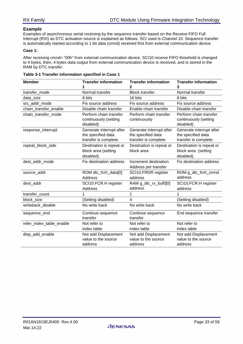
Example Examples of asynchronous serial receiving by the sequence transfer based on the Receive FIFO Full Interrupt (RXI) as DTC activation source is explained as follows. SCI used is Channel 10. Sequence transfer is automatically started according to 1 bit data (cmnd) received first from external communication device.
Case 1: After receiving cmnd= ”00h” from external communication device, SCI10 receive FIFO threshold is changed to 4 bytes, then, 4 bytes data output from external communication device is received, and is stored in the RAM by DTC transfer.
Table 3-1 Transfer information specified in Case 1
Member Transfer information 1
Transfer information 2
Transfer information 3
transfer_mode Normal transfer Block transfer Normal transfer data_size 8 bits 16 bits 8 bits src_addr_mode Fix source address Fix source address Fix source address chain_transfer_enable Disable chain transfer Enable chain transfer Disable chain transfer chain_transfer_mode Perform chain transfer
continuously (setting disabled)
Perform chain transfer continuously
Perform chain transfer continuously (setting disabled)
response_interrupt Generate interrupt after the specified data transfer is complete.
Generate interrupt after the specified data transfer is complete.
Generate interrupt after the specified data transfer is complete.
repeat_block_side Destination is repeat or block area (setting disabled)
Destination is repeat or block area
Destination is repeat or block area (setting disabled)
dest_addr_mode Fix destination address Increment destination Address per transfer
Fix destination address
source_addr ROM dtc_fcrh_data[0] Address
SCI10.FRDR register address
ROM g_dtc_fcrh_cmnd address
dest_addr SCI10.FCR.H register Address
RAM g_dtc_rx_buf0[0] address
SCI10.FCR.H register address
transfer_count 1 1 1 block_size (Setting disabled) 4 (Setting disabled) writeback_disable No write back No write back No write back
sequence_end Continue sequence transfer
Continue sequence transfer
End sequence transfer
refer_index_table_enable Not refer to index table
Not refer to index table
Not refer to index table
disp_add_enable Not add Displacement value to the source address
Not add Displacement value to the source address
Not add Displacement value to the source address
RX Family DTC Module Using Firmware Integration Technology
R01AN1819EJ0400 Rev.4.00 Page 34 of 59 Mar.14.22
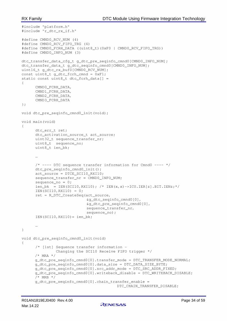
#include "platform.h" #include "r_dtc_rx_if.h" #define CMND0_RCV_NUM (4) #define CMND0_RCV_FIFO_TRG (4) #define CMND0_FCRH_DATA ((uint8_t)(0xF0 | CMND0_RCV_FIFO_TRG)) #define CMND0_INFO_NUM (3) dtc_transfer_data_cfg_t g_dtc_pre_seqinfo_cmnd0[CMND0_INFO_NUM]; dtc_transfer_data_t g_dtc_seqinfo_cmnd0[CMND0_INFO_NUM]; uint16_t g_dtc_rx_buf0[CMND0_RCV_NUM]; const uint8_t g_dtc_fcrh_cmnd = 0xF1; static const uint8_t dtc_fcrh_data[] = {
CMND0_FCRH_DATA, CMND1_FCRH_DATA, CMND2_FCRH_DATA, CMND3_FCRH_DATA
}; void dtc_pre_seqinfo_cmnd0_init(void); void main(void) {
dtc_err_t ret; dtc_activation_source_t act_source; uint32_t sequence_transfer_nr; uint8_t sequence_no; uint8_t ien_bk; … /* ---- DTC sequence transfer information for Cmnd0 ---- */ dtc_pre_seqinfo_cmnd0_init(); act_source = DTCE_SCI10_RXI10; sequence_transfer_nr = CMND0_INFO_NUM; sequence_no = 0; ien_bk = IEN(SCI10,RXI10); /* IEN(x,x)->ICU.IER[z].BIT.IENz;*/ IEN(SCI10,RXI10) = 0; ret = R_DTC_CreateSeq(act_source,
&g_dtc_seqinfo_cmnd0[0], &g_dtc_pre_seqinfo_cmnd0[0], sequence_transfer_nr, sequence_no);
IEN(SCI10,RXI10)= ien_bk;
… } void dtc_pre_seqinfo_cmnd0_init(void) {
/* [1st] Sequence transfer information – Changing the SCI10 Receive FIFO trigger */
/* MRA */ g_dtc_pre_seqinfo_cmnd0[0].transfer_mode = DTC_TRANSFER_MODE_NORMAL; g_dtc_pre_seqinfo_cmnd0[0].data_size = DTC_DATA_SIZE_BYTE; g_dtc_pre_seqinfo_cmnd0[0].src_addr_mode = DTC_SRC_ADDR_FIXED; g_dtc_pre_seqinfo_cmnd0[0].writeback_disable = DTC_WRITEBACK_DISABLE; /* MRB */ g_dtc_pre_seqinfo_cmnd0[0].chain_transfer_enable =
DTC_CHAIN_TRANSFER_DISABLE;
RX Family DTC Module Using Firmware Integration Technology
R01AN1819EJ0400 Rev.4.00 Page 35 of 59 Mar.14.22
g_dtc_pre_seqinfo_cmnd0[0].chain_transfer_mode = DTC_CHAIN_TRANSFER_CONTINUOUSLY;
g_dtc_pre_seqinfo_cmnd0[0].response_interrupt = DTC_INTERRUPT_AFTER_ALL_COMPLETE;
g_dtc_pre_seqinfo_cmnd0[0].repeat_block_side = DTC_REPEAT_BLOCK_DESTINATION;
g_dtc_pre_seqinfo_cmnd0[0].dest_addr_mode = DTC_DES_ADDR_FIXED; g_dtc_pre_seqinfo_cmnd0[0].refer_index_table_enable =
DTC_REFER_INDEX_TABLE_DISABLE; g_dtc_pre_seqinfo_cmnd0[0].sequence_end =
DTC_SEQUENCE_TRANSFER_CONTINUE; /* MRC */ g_dtc_pre_seqinfo_cmnd0[0].disp_add_enable =
DTC_SRC_ADDR_DISP_ADD_DISABLE; /* SAR */ g_dtc_pre_seqinfo_cmnd0[0].source_addr = (uint32_t)&dtc_fcrh_data[0]; /* DAR */ g_dtc_pre_seqinfo_cmnd0[0].dest_addr = (uint32_t)&SCI10.FCR.BYTE.H; /* CRA, CRB */ g_dtc_pre_seqinfo_cmnd0[0].transfer_count = 1;
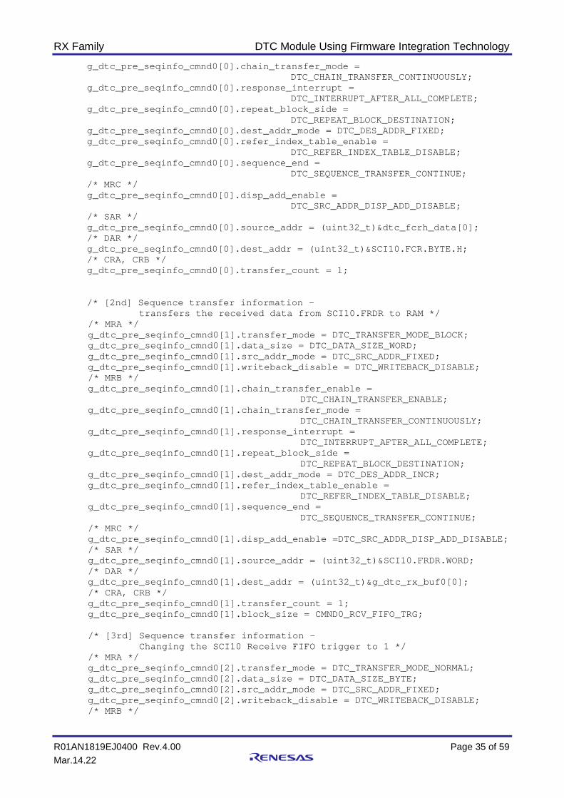
/* [2nd] Sequence transfer information – transfers the received data from SCI10.FRDR to RAM */
/* MRA */ g_dtc_pre_seqinfo_cmnd0[1].transfer_mode = DTC_TRANSFER_MODE_BLOCK; g_dtc_pre_seqinfo_cmnd0[1].data_size = DTC_DATA_SIZE_WORD; g_dtc_pre_seqinfo_cmnd0[1].src_addr_mode = DTC_SRC_ADDR_FIXED; g_dtc_pre_seqinfo_cmnd0[1].writeback_disable = DTC_WRITEBACK_DISABLE; /* MRB */ g_dtc_pre_seqinfo_cmnd0[1].chain_transfer_enable =
DTC_CHAIN_TRANSFER_ENABLE; g_dtc_pre_seqinfo_cmnd0[1].chain_transfer_mode =
DTC_CHAIN_TRANSFER_CONTINUOUSLY; g_dtc_pre_seqinfo_cmnd0[1].response_interrupt =
DTC_INTERRUPT_AFTER_ALL_COMPLETE; g_dtc_pre_seqinfo_cmnd0[1].repeat_block_side =
DTC_REPEAT_BLOCK_DESTINATION; g_dtc_pre_seqinfo_cmnd0[1].dest_addr_mode = DTC_DES_ADDR_INCR; g_dtc_pre_seqinfo_cmnd0[1].refer_index_table_enable =
DTC_REFER_INDEX_TABLE_DISABLE; g_dtc_pre_seqinfo_cmnd0[1].sequence_end =
DTC_SEQUENCE_TRANSFER_CONTINUE; /* MRC */ g_dtc_pre_seqinfo_cmnd0[1].disp_add_enable =DTC_SRC_ADDR_DISP_ADD_DISABLE; /* SAR */ g_dtc_pre_seqinfo_cmnd0[1].source_addr = (uint32_t)&SCI10.FRDR.WORD; /* DAR */ g_dtc_pre_seqinfo_cmnd0[1].dest_addr = (uint32_t)&g_dtc_rx_buf0[0]; /* CRA, CRB */ g_dtc_pre_seqinfo_cmnd0[1].transfer_count = 1; g_dtc_pre_seqinfo_cmnd0[1].block_size = CMND0_RCV_FIFO_TRG;
/* [3rd] Sequence transfer information –
Changing the SCI10 Receive FIFO trigger to 1 */ /* MRA */ g_dtc_pre_seqinfo_cmnd0[2].transfer_mode = DTC_TRANSFER_MODE_NORMAL; g_dtc_pre_seqinfo_cmnd0[2].data_size = DTC_DATA_SIZE_BYTE; g_dtc_pre_seqinfo_cmnd0[2].src_addr_mode = DTC_SRC_ADDR_FIXED; g_dtc_pre_seqinfo_cmnd0[2].writeback_disable = DTC_WRITEBACK_DISABLE; /* MRB */
RX Family DTC Module Using Firmware Integration Technology
R01AN1819EJ0400 Rev.4.00 Page 36 of 59 Mar.14.22
g_dtc_pre_seqinfo_cmnd0[2].chain_transfer_enable = DTC_CHAIN_TRANSFER_DISABLE;
g_dtc_pre_seqinfo_cmnd0[2].chain_transfer_mode = DTC_CHAIN_TRANSFER_CONTINUOUSLY;
g_dtc_pre_seqinfo_cmnd0[2].response_interrupt = DTC_INTERRUPT_AFTER_ALL_COMPLETE;
g_dtc_pre_seqinfo_cmnd0[2].repeat_block_side = DTC_REPEAT_BLOCK_DESTINATION;
g_dtc_pre_seqinfo_cmnd0[2].dest_addr_mode = DTC_DES_ADDR_FIXED; g_dtc_pre_seqinfo_cmnd0[2].refer_index_table_enable=
DTC_REFER_INDEX_TABLE_DISABLE; g_dtc_pre_seqinfo_cmnd0[2].sequence_end = DTC_SEQUENCE_TRANSFER_END; /* MRC */ g_dtc_pre_seqinfo_cmnd0[2].disp_add_enable =DTC_SRC_ADDR_DISP_ADD_DISABLE; /* SAR */ g_dtc_pre_seqinfo_cmnd0[2].source_addr = (uint32_t)&g_dtc_fcrh_cmnd; /* DAR */ g_dtc_pre_seqinfo_cmnd0[2].dest_addr = (uint32_t)&SCI10.FCR.BYTE.H; /* CRA, CRB */ g_dtc_pre_seqinfo_cmnd0[2].transfer_count = 1;
}
Case 2 : When receiving cmnd >= “04h” from external communication device, generate the interrupt to CPU without sequence transfer. #include "platform.h" #include "r_dtc_rx_if.h" void main(void) {
dtc_err_t ret; dtc_activation_source_t act_source; uint32_t sequence_transfer_nr; uint8_t sequence_no; uint8_t ien_bk; uint16_t i; … /* ---- DTC sequence transfer information for Cmnd4-Cmnd255 ---- */ for (i = 4; i < 256; i++) {
act_source = DTCE_SCI10_RXI10; sequence_transfer_nr = 0; sequence_no = i; ien_bk = IEN(SCI10,RXI10); /* IEN(x,x)->ICU.IER[z].BIT.IENz;*/ IEN(SCI10,RXI10) = 0; ret = R_DTC_CreateSeq(act_source,
NULL, NULL, sequence_transfer_nr, sequence_no);
IEN(SCI10,RXI10) = ien_bk; }
…
RX Family DTC Module Using Firmware Integration Technology
R01AN1819EJ0400 Rev.4.00 Page 37 of 59 Mar.14.22
Special Notes: Before calling R_DTC_CreateSeq(), user must disable the current interrupt request (the interrupt source is passed to R_DTC_CreateSeq()) by clearing Interrupt Request Enable bit (IERm.IENj):
ICU.IER[m].BIT.IENj = 0;
Then, enable the interrupt request disabled after R_DTC_CreateSeq() is ended.
The correspondence between IERm.IENj bit and interrupt source is described in Interrupt Vector Table, chapter Interrupt Controller (ICU) of User’s Manual: Hardware.
RX Family DTC Module Using Firmware Integration Technology
R01AN1819EJ0400 Rev.4.00 Page 38 of 59 Mar.14.22
R_DTC_Control() This function controls the operation of the DTC.
Format dtc_err_t R_DTC_Control (
dtc_command_t command,
dtc_stat_t * p_stat,
dtc_cmd_arg_t * p_args
)
Parameters dtc_command_t command DTC control command
dtc_stat_t * p_stat Pointer to the status when command is DTC_CMD_STATUS_GET.
Member of dtc_stat_t Structure
Member Short Description
Setting Value Setting Details
vect_nr DTC-Activating Vector Number
Vector Number Monitoring
The value is only valid when DTC transfer is in progress (the value of the DTC Active Flag is 1).
in_progress DTC Active Flag - false - true
- DTC transfer operation is not in progress. - DTC transfer operation is in progress.
dtc_cmd_arg_t * p_args Pointer to the argument structure when command is DTC_CMD_ACT_SRC_ENABLE, DTC_CMD_ACT_SRC_DISABLE, DTC_CMD_CHAIN_TRANSFER_ABORT, DTC_CMD_SEQUENCE_TRANSFER_ENABLE, or DTC_CMD_CHANGING_DATA_FORCIBLY_SET.
Members of dtc_cmd_arg_t Structure
Member Short Description Setting Details act_src DTC-Activating Vector
Number The value is only valid when command is DTC_CMD_ACT_SRC_ENABLE or DTC_CMD_ACT_SRC_DISABLE or DTC_CMD_SEQUENCE_TRANSFER_ENABLE or DTC_CMD_CHANGING_DATA_FORCIBLY_SET
chain_transfer_nr Number of chain transfer (Note)
The value is only valid when command is DTC_CMD_CHAIN_TRANSFER_ABORT or DTC_CMD_CHANGING_DATA_FORCIBLY_SET.
*p_transfer_data Pointer to start address of Transfer data area on RAM
The value is only valid when command is DTC_CMD_CHANGING_DATA_FORCIBLY_SET.
*p_data_cfg Pointer to settings for Transfer data
The value is only valid when command is DTC_CMD_CHANGING_DATA_FORCIBLY_SET.
Note: Set the value as same as the argument chain_transfer_nr when user call R_DTC_Create() before.
RX Family DTC Module Using Firmware Integration Technology
R01AN1819EJ0400 Rev.4.00 Page 39 of 59 Mar.14.22
Return Values [DTC_SUCCESS] /* Successful operation */ [DTC_ERR_NOT_OPEN] /* DTC is not initialized yet. */ [DTC_ERR_INVALID_COMMAND] /* Command parameters are invalid or DTC_CMD_CHANGING_DATA_FORCIBLY_SET command error. */ [DTC_ERR_NULL_PTR] /* Argument pointers are NULL. */ [DTC_ERR_ACT] /* Data transfer is in progress. */
Properties Prototype declarations are contained in r_dtc_rx_if.h.
Description Processing is performed depending on the command.
Command Arguments dtc_stat_t *
Arguments dtc_cmd_arg_t *
Description
DTC_CMD_DTC_START
NULL NULL Starts DTC module using DTC Module Start (DTCST) bit.
DTC_CMD_DTC_STOP
NULL NULL Stops DTC module using DTC Module Start (DTCST) bit.
DTC_CMD_DATA_READ_SKIP_ENABLE
NULL NULL Enables Transfer Data Read Skip using DTC Transfer Information Read Skip Enable (RRS) bit.
DTC_CMD_DATA_READ_SKIP_DISABLE
NULL NULL Disables Transfer Data Read Skip using DTC Transfer Information Read Skip Enable (RRS) bit.
DTC_CMD_ACT_SRC_ENABLE
NULL p_args->act_src Sets an interrupt source using DTC Start Enable (DTCE) bit.
DTC_CMD_ACT_SRC_DISABLE
NULL p_args->act_src Clears an interrupt source using DTC Start Enable (DTCE) bit.
DTC_CMD_STATUS_GET
p_stat->in_progress p_stat->vect_nr
NULL Gets a DTC Active Flag (ACT) and vector number (VECN[7:0]) using DTC Status Register (DTCSTS).
DTC_CMD_CHAIN_TRANSFER_ABORT
NULL p_args-> chain_transfer_nr
Aborts the current active chain transfer.
DTC_CMD_SEQUENCE_TRANSFER_ENABLE
NULL p_args->act_src Specifies Sequence Transfer Vector number and enables Sequence transfer using DTC Sequence Transfer Enable Register (DTCSEQ).
DTC_CMD_SEQUENCE_TRANSFER_DISABLE
NULL NULL Disables Sequence Transfer using DTC Sequence Transfer Enable Register (DTCSEQ).
DTC_CMD_SEQUENCE_TRANSFER_ABORT
NULL NULL Aborts Sequence Transfer using Sequence Transfer End bit (SQTFRL).
DTC_CMD_CHANGING_DATA_FORCIBLY_SET
NULL p_args->act_src p_args->chain_transfer_nr p_args->p_transfer_data p_args->p_data_cfg
Changes the value set by R_DTC_Create(). It is a valid process for changing parameters*1 forcibly set by R_DTC_Create().
Note: 1. writeback_disable, sequence_end, refer_index_table_enable, and disp_add_enable
Example Case 1: Start DTC module
RX Family DTC Module Using Firmware Integration Technology
R01AN1819EJ0400 Rev.4.00 Page 40 of 59 Mar.14.22
dtc_err_t ret; /* Start DTC module */ ret = R_DTC_Control(DTC_CMD_DTC_START, NULL, NULL); Case 2: Stop DTC module dtc_err_t ret; /* Stop DTC module */ ret = R_DTC_Control(DTC_CMD_DTC_STOP, NULL, NULL); Case 3 : Enable transfer information read skip dtc_err_t ret; /* Enable transfer information read skip */ ret = R_DTC_Control(DTC_CMD_DATA_READ_SKIP_ENABLE, NULL, NULL); Case 4: Disable transfer information read skip dtc_err_t ret; /* Disable transfer information read skip */ ret = R_DTC_Control(DTC_CMD_DATA_READ_SKIP_DISABLE, NULL, NULL); Case 5 : Using the DTCE, set the interrupt used for DTC activation source dtc_err_t ret; dtc_cmd_arg_t args; /* Disable DTC transfer request by SCI10 receive data full interrupt */ IEN(SCI10, RXI10) = 0; /* Set SCI10 receive data full interrupt as DTC activation source*/ args.act_src = DTCE_SCI10_RXI10; /* Set the interrupt used for DTC activation source */ ret = R_DTC_Control(DTC_CMD_ACT_SRC_ENABLE, NULL, &args); Case 6 : Using the DTCE, clear the interrupt used for DTC activation source dtc_err_t ret; dtc_cmd_arg_t args; /* Disable DTC trasnfer request by SCI10 receive data full interrupt */ IEN(SCI10, RXI10) = 0; /* Set SCI10 receive data full interrupt as DTC activation source */ args.act_src = DTCE_SCI10_RXI10; /* Delete the interrupt used for DTC activation source */ ret = R_DTC_Control(DTC_CMD_ACT_SRC_DISABLE, NULL, &args);
RX Family DTC Module Using Firmware Integration Technology
R01AN1819EJ0400 Rev.4.00 Page 41 of 59 Mar.14.22
Case 7 : Get DTC Active Flag (ACT) and Vector number (VECN[7:0]) in progress dtc_err_t ret; dtc_stat_t stat; uint8_t interrupt_number; /* Get DTC Active Flag (ACT) and Vector number(VECN[7:0])in progress */ ret = R_DTC_Control(DTC_CMD_STATUS_GET, stat, NULL); if (true == stat.in_progress) { /* Vector number is valid */ interrupt_number = stat.vect_nr; } else { /* Vector number is inbalid */ } Case 8 : Abort the chain transfer in process dtc_err_t ret; dtc_cmd_arg_t args; /* No. Of chain transfer = 5 */ args. chain_transfer_nr = 5; /* Abort the chain transfer in process */ ret = R_DTC_Control(DTC_CMD_STATUS_GET, NULL, &args); Case 9 : Enable the sequence transfer dtc_err_t ret; dtc_cmd_arg_t args; /* Set SCI10 receive data full interrupt as sequence transfger activation source */ args.act_src = DTCE_SCI10_RXI10; /* Enable sequence transfer */ ret = R_DTC_Control(DTC_CMD_SEQUENCE_TRANSFER_ENABLE, NULL, &args); Case 10: Disable the sequence transfer dtc_err_t ret; /* Disable sequence transfer */ ret = R_DTC_Control(DTC_CMD_SEQUENCE_TRANSFER_DISABLE, NULL, NULL); Case 11: Abort the sequence transfer dtc_err_t ret; /* Disable DTC transfer request by SCI10 receive data full interrupt */ IEN(SCI10, RXI10) = 0; /* Issue command repeatedly until sequence transfer can be aborted */ do { ret = R_DTC_Control(DTC_CMD_SEQUENCE_TRANSFER_ABORT, NULL, NULL); } while (DTC_ERR_ACT == ret);
RX Family DTC Module Using Firmware Integration Technology
R01AN1819EJ0400 Rev.4.00 Page 42 of 59 Mar.14.22
Case 12: Changes the value set by R_DTC_Create() dtc_activation_source_t act_source; uint32_t chain_transfer_nr; act_source = DTCE_SCI10_RXI10; chain_transfer_nr = 0; if (R_DTC_Create(act_source, &g_dtc_info_sqnum, &g_dtc_pre_info_sqnum, chain_transfer_nr) != DTC_SUCCESS) { /* Error */ } g_dtc_pre_info_sqnum.writeback_disable = DTC_WRITEBACK_DISABLE; g_dtc_pre_info_sqnum.sequence_end = DTC_SEQUENCE_TRANSFER_CONTINUE; g_dtc_pre_info_sqnum.refer_index_table_enable = DTC_REFER_INDEX_TABLE_ENABLE; g_dtc_pre_info_sqnum.disp_add_enable = DTC_SRC_ADDR_DISP_ADD_DISABLE; args.act_src = DTCE_SCI10_RXI10; args.chain_transfer_nr = 0; args.p_transfer_data = &g_dtc_info_sqnum; args.p_data_cfg = &g_dtc_pre_info_sqnum; if (R_DTC_Control(DTC_CMD_CHANGING_DATA_FORCIBLY_SET, NULL, &args) != DTC_SUCCESS) { /* Error */ }
Special Notes: When the command is DTC_CMD_GET_STATUS, the vector number is valid if only the DTC is in the progress (p_stat->in_progress is true).
With command DTC_CMD_ENABLE_ACT_SRC, DTC_CMD_DISABLE_ACT_SRC or DTC_CMD_SEQUENCE_TRANSFER_ABORT, before calling R_DTC_Control(), user must disable the current interrupt request (the interrupt source is passed to R_DTC_Control()) by clearing Interrupt Request Enable bit (IERm.IENj); ICU.IER[m].BIT.IENj = 0; After processing of R_DTC_Control() is ended, the interrupt request disabled is enabled.
The correspondence between IERm.IENj bit and interrupt source is described in Interrupt Vector Table, chapter Interrupt Controller (ICU) of User’s Manual: Hardware.
With abort processing, user must re-create the Chain transfer data after the transfer is aborted because the old Transfer data are destroyed.
If an invalid value is attempted to set with DTC_CMD_CHANGING_DATA_FORCIBLY_SET, R_DTC_Control() returns DTC_ERR_INVALID_COMMAND
R_DTC_Control() may already update some registers before the invalid value is detected. This occurs only when users try to change FORCIBLY DTC with Invalid Value.
RX Family DTC Module Using Firmware Integration Technology
R01AN1819EJ0400 Rev.4.00 Page 43 of 59 Mar.14.22
R_DTC_GetVersion() This function is used to get the driver version information.
Format uint32_t R_DTC_GetVersion (void)
Parameters None.
Return Values Version number
Upper 2 bytes: major version, lower 2 bytes: minor version
Properties Prototype declarations are contained in r_dtc_rx_if.h.
Description Returns the version information.
Example uint32_t version; version = R_DTC_GetVersion();
Special Notes: None.
4. Pin Setting DTC FIT module don’t use pin setting.
RX Family DTC Module Using Firmware Integration Technology
R01AN1819EJ0400 Rev.4.00 Page 44 of 59 Mar.14.22
5. Demo Projects Demo projects include function main() that utilizes the FIT module and its dependent modules (e.g. r_bsp). This FIT module includes the following demo projects.
5.1 dtc_demo_rskrx231, dtc_demo_rskrx231_gcc The dtc_demo_rskrx231, dtc_demo_rskrx231_gcc program demonstrates how to set up a DTC in repeat transfer mode to handle ADC conversion result. As the program runs, the DTC save ADC conversion result to a buffer of 32 bytes in sequence.
5.2 dtc_demo_rskrx65n_2m, dtc_demo_rskrx65n_2m_gcc The dtc_demo_rskrx65n_2m, dtc_demo_rskrx65n_2m_gcc program is identical to dtc_demo_rskrx231.
5.3 dtc_demo_rskrx130, dtc_demo_rskrx130_gcc The dtc_demo_rskrx130, dtc_demo_rskrx130_gcc program is identical to dtc_demo_rskrx231.
5.4 dtc_demo_rskrx72m, dtc_demo_rskrx72m_gcc The dtc_demo_rskrx72m, dtc_demo_rskrx72m_gcc program is identical to dtc_demo_rskrx231.
5.5 dtc_demo_rskrx671, dtc_demo_rskrx671_gcc The dtc_demo_rskrx671, dtc_demo_rskrx671_gcc program is identical to dtc_demo_rskrx231.
5.6 Adding a Demo to a Workspace Demo projects are found in the FITDemos subdirectory of the distribution file for this application note. To add a demo project to a workspace, select File >> Import >> General >> Existing Projects into Workspace, then click “Next”. From the Import Projects dialog, choose the “Select archive file” radio button. “Browse” to the FITDemos subdirectory, select the desired demo zip file, then click “Finish”.
5.7 Downloading Demo Projects Demo projects are not included in the RX Driver Package. When using the demo project, the FIT module needs to be downloaded. To download the FIT module, right click on this application note and select “Sample Code (download)” from the context menu in the Smart Browser >> Application Notes tab.
RX Family DTC Module Using Firmware Integration Technology
R01AN1819EJ0400 Rev.4.00 Page 45 of 59 Mar.14.22
6. Appendices 6.1 Confirmed Operation Environment This section describes confirmed operation environment for the DTC FIT module.
Table 6.1 Confirmed Operation Environment (Rev.4.00)
Item Contents Integrated development environment
Renesas Electronics e2 studio Version 2022-01 IAR Embedded Workbench for Renesas RX 4.20.3
C compiler Renesas Electronics C/C++ Compiler Package for RX Family V3.04.00 Compiler option: The following option is added to the default settings of the integrated development environment. -lang = c99
GCC for Renesas RX 8.3.0.202104 Compiler option: The following option is added to the default settings of the integrated development environment. -std=gnu99 Linker option: The following user defined option should be added to the default settings of the integrated development environment, if “Optimize size (-Os)” is used: -Wl,--no-gc-sections This is to work around a GCC linker issue whereby the linker erroneously discard interrupt functions declared in FIT peripheral module
IAR C/C++ Compiler for Renesas RX version 4.20.3 Compiler option: The default settings of the integrated development environment.
Endian Big endian/little endian Revision of the module Rev.4.00 Board used Target board for RX140 (Part Number.: RTK55140xxxxxxxxxx)
Renesas Starter Kit for RX66T (product No: RTK50566T0SxxxxxBE)
Table 6.2 Confirmed Operation Environment (Rev.3.90)
Item Contents Integrated development environment
Renesas Electronics e2 studio Version 2021-07 IAR Embedded Workbench for Renesas RX 4.20.3
C compiler Renesas Electronics C/C++ Compiler Package for RX Family V3.03.00 Compiler option: The following option is added to the default settings of the integrated development environment. -lang = c99
GCC for Renesas RX 8.3.0.202004 Compiler option: The following option is added to the default settings of the integrated development environment. -std=gnu99 Linker option: The following user defined option should be added to the default settings of the integrated development environment, if “Optimize size (-Os)” is used: -Wl,--no-gc-sections This is to work around a GCC linker issue whereby the linker erroneously discard interrupt functions declared in FIT peripheral module
IAR C/C++ Compiler for Renesas RX version 4.20.3 Compiler option: The default settings of the integrated development environment.
Endian Big endian/little endian Revision of the module Rev.3.90 Board used Renesas Starter Kit+ for RX671 (product No.: RTK55671xxxxxxxxxx)
RX Family DTC Module Using Firmware Integration Technology
R01AN1819EJ0400 Rev.4.00 Page 46 of 59 Mar.14.22
Table 6.3 Confirmed Operation Environment (Rev.3.80)
Item Contents Integrated development environment
Renesas Electronics e2 studio Version 2021-07 IAR Embedded Workbench for Renesas RX 4.20.3
C compiler Renesas Electronics C/C++ Compiler Package for RX Family V3.03.00 Compiler option: The following option is added to the default settings of the integrated development environment. -lang = c99
GCC for Renesas RX 8.3.0.202004 Compiler option: The following option is added to the default settings of the integrated development environment. -std=gnu99 Linker option: The following user defined option should be added to the default settings of the integrated development environment, if “Optimize size (-Os)” is used: -Wl,--no-gc-sections This is to work around a GCC linker issue whereby the linker erroneously discard interrupt functions declared in FIT peripheral module
IAR C/C++ Compiler for Renesas RX version 4.20.3 Compiler option: The default settings of the integrated development environment.
Endian Big endian/little endian Revision of the module Rev.3.80 Board used Target board for RX140 (Part Number.: RTK5RX140xxxxxxxxx)
RX Family DTC Module Using Firmware Integration Technology
R01AN1819EJ0400 Rev.4.00 Page 47 of 59 Mar.14.22
Table 6.4 Confirmed Operation Environment (Rev.3.70)
Item Contents Integrated development environment
Renesas Electronics e2 studio Version 2021-07 IAR Embedded Workbench for Renesas RX 4.20.3
C compiler Renesas Electronics C/C++ Compiler Package for RX Family V3.03.00 Compiler option: The following option is added to the default settings of the integrated development environment. -lang = c99
GCC for Renesas RX 8.3.0.202004 Compiler option: The following option is added to the default settings of the integrated development environment. -std=gnu99 Linker option: The following user defined option should be added to the default settings of the integrated development environment, if “Optimize size (-Os)” is used: -Wl,--no-gc-sections This is to work around a GCC linker issue whereby the linker erroneously discard interrupt functions declared in FIT peripheral module
IAR C/C++ Compiler for Renesas RX version 4.20.3 Compiler option: The default settings of the integrated development environment.
Endian Big endian/little endian Revision of the module Rev.3.70 Board used Renesas Starter Kit+ for RX671 (product No.: RTK55671xxxxxxxxxx) Table 6.5 Confirmed Operation Environment (Rev.3.60)
Item Contents Integrated development environment
Renesas Electronics e2 studio Version 7.8.0
C compiler Renesas Electronics C/C++ Compiler Package for RX Family V3.02.00 Compiler option: The following option is added to the default settings of the integrated development environment. -lang = c99
GCC for Renesas RX 8.3.0.201904 Compiler option: The following option is added to the default settings of the integrated development environment. -std=gnu99 Linker option: The following user defined option should be added to the default settings of the integrated development environment, if “Optimize size (-Os)” is used: -Wl,--no-gc-sections This is to work around a GCC linker issue whereby the linker erroneously discard interrupt functions declared in FIT peripheral module
Endian Little endian Revision of the module Rev.3.60 Board used Renesas Starter Kit+ for RX72M (product No.: RTK5572Mxxxxxxxxxx)
Renesas Starter Kit+ for RX65N-2MB (product No.: RTK50565N2CxxxxxBR) Renesas Starter Kit for RX130 (product No.: RTK5005130SxxxxxBE) Renesas Starter Kit+ for RX231 (product No.: RTK505231xxxxxxxx)
RX Family DTC Module Using Firmware Integration Technology
R01AN1819EJ0400 Rev.4.00 Page 48 of 59 Mar.14.22
Table 6.6 Confirmed Operation Environment (Rev.3.50)
Item Contents Integrated development environment
Renesas Electronics e2 studio Version 7.7.0 IAR Embedded Workbench for Renesas RX 4.12.1
C compiler Renesas Electronics C/C++ Compiler Package for RX Family V3.02.00 Compiler option: The following option is added to the default settings of the integrated development environment. -lang = c99
GCC for Renesas RX 8.3.0.201904 Compiler option: The following option is added to the default settings of the integrated development environment. -std=gnu99 Linker option: The following user defined option should be added to the default settings of the integrated development environment, if “Optimize size (-Os)” is used: -Wl,--no-gc-sections This is to work around a GCC linker issue whereby the linker erroneously discard interrupt functions declared in FIT peripheral module
IAR C/C++ Compiler for Renesas RX version 4.12.1 Compiler option: The default settings of the integrated development environment.
Endian Big endian/little endian Revision of the module Rev.3.50 Board used Renesas Solution Starter Kit+ for RX23E-A
(product No.: RTK0ESXBxxxxxxxxxx) Table 6.7 Confirmed Operation Environment (Rev.3.40)
Item Contents Integrated development environment
Renesas Electronics e2 studio Version 7.7.0 IAR Embedded Workbench for Renesas RX 4.12.1
C compiler Renesas Electronics C/C++ Compiler Package for RX Family V3.01.00 Compiler option: The following option is added to the default settings of the integrated development environment. -lang = c99
GCC for Renesas RX 4.8.4.201902 Compiler option: The following option is added to the default settings of the integrated development environment. -std=gnu99 Linker option: The following user defined option should be added to the default settings of the integrated development environment, if “Optimize size (-Os)” is used: -Wl,--no-gc-sections This is to work around a GCC linker issue whereby the linker erroneously discard interrupt functions declared in FIT peripheral module
IAR C/C++ Compiler for Renesas RX version 4.12.1 Compiler option: The default settings of the integrated development environment.
Endian Big endian/little endian Revision of the module Rev.3.40 Board used Renesas Starter Kit+ for RX72N (product No.: RTK5572Nxxxxxxxxxx)
RX Family DTC Module Using Firmware Integration Technology
R01AN1819EJ0400 Rev.4.00 Page 49 of 59 Mar.14.22
Table 6.8 Confirmed Operation Environment (Rev.3.30)
Item Contents Integrated development environment
Renesas Electronics e2 studio Version 7.7.0
C compiler Renesas Electronics C/C++ Compiler Package for RX Family V3.01.00 Compiler option: The following option is added to the default settings of the integrated development environment. -lang = c99
GCC for Renesas RX 4.8.4.201902 Compiler option: The following option is added to the default settings of the integrated development environment. -std=gnu99 Linker option: The following user defined option should be added to the default settings of the integrated development environment, if “Optimize size (-Os)” is used: -Wl,--no-gc-sections This is to work around a GCC linker issue whereby the linker erroneously discard interrupt functions declared in FIT peripheral module
Endian Big endian/little endian Revision of the module Rev.3.30 Board used RX13T CPU Card (product No.: RTK0EMXA10C00000BJ)
Table 6.9 Confirmed Operation Environment (Rev.3.21)
Item Contents Integrated development environment
Renesas Electronics e2 studio Version 7.5.0 IAR Embedded Workbench for Renesas RX 4.12.1
C compiler Renesas Electronics C/C++ Compiler Package for RX Family V3.01.00 Compiler option: The following option is added to the default settings of the integrated development environment. -lang = c99
GCC for Renesas RX 4.8.4.201902 Compiler option: The following option is added to the default settings of the integrated development environment. -std=gnu99 Linker option: The following user defined option should be added to the default settings of the integrated development environment, if “Optimize size (-Os)” is used: -Wl,--no-gc-sections This is to work around a GCC linker issue whereby the linker erroneously discard interrupt functions declared in FIT peripheral module
IAR C/C++ Compiler for Renesas RX version 4.12.1 Compiler option: The default settings of the integrated development environment.
Endian Big endian/little endian Revision of the module Rev.3.21 Board used Renesas Solution Starter Kit for RX23W (product No.: RTK5523Wxxxxxxxxxx)
RX Family DTC Module Using Firmware Integration Technology
R01AN1819EJ0400 Rev.4.00 Page 50 of 59 Mar.14.22
Table 6.10 Confirmed Operation Environment (Rev.3.20)
Item Contents Integrated development environment
Renesas Electronics e2 studio Version 7.5.0 IAR Embedded Workbench for Renesas RX 4.12.1
C compiler Renesas Electronics C/C++ Compiler Package for RX Family V3.01.00 Compiler option: The following option is added to the default settings of the integrated development environment. -lang = c99
GCC for Renesas RX 4.8.4.201902 Compiler option: The following option is added to the default settings of the integrated development environment. -std=gnu99 Linker option: The following user defined option should be added to the default settings of the integrated development environment, if “Optimize size (-Os)” is used: -Wl,--no-gc-sections This is to work around a GCC linker issue whereby the linker erroneously discard interrupt functions declared in FIT peripheral module
IAR C/C++ Compiler for Renesas RX version 4.12.1 Compiler option: The default settings of the integrated development environment.
Endian Big endian/little endian Revision of the module Rev.3.20 Board used Renesas Starter Kit+ for RX72M (product No.: RTK5572Mxxxxxxxxxx) Table 6.11 Confirmed Operation Environment (Rev.3.10)
Item Contents Integrated development environment
Renesas Electronics e2 studio Version 7.5.0
C compiler Renesas Electronics C/C++ Compiler Package for RX Family V3.01.00 Compiler option: The following option is added to the default settings of the integrated development environment. -lang = c99
Endian Big endian/little endian Revision of the module Rev.3.10 Board used Renesas Solution Starter Kit for RX23W (product No.: RTK5523Wxxxxxxxxxx)
RX Family DTC Module Using Firmware Integration Technology
R01AN1819EJ0400 Rev.4.00 Page 51 of 59 Mar.14.22
Table 6.12 Confirmed Operation Environment (Rev.3.01)
Item Contents Integrated development environment
Renesas Electronics e2 studio Version 7.4.0 IAR Embedded Workbench for Renesas RX 4.10.1
C compiler Renesas Electronics C/C++ Compiler Package for RX Family V3.01.00 Compiler option: The following option is added to the default settings of the integrated development environment. -lang = c99
GCC for Renesas RX 4.8.4.201803 Compiler option: The following option is added to the default settings of the integrated development environment. -std=gnu99 Linker option: The following user defined option should be added to the default settings of the integrated development environment, if “Optimize size (-Os)” is used: -Wl,--no-gc-sections This is to work around a GCC linker issue whereby the linker erroneously discard interrupt functions declared in FIT peripheral module
IAR C/C++ Compiler for Renesas RX version 4.10.1 Compiler option: The default settings of the integrated development environment.
Endian Big endian/little endian Revision of the module Rev.3.01 Board used Renesas Starter Kit+ for RX65N-2MB (product No.: RTK50565Nxxxxxxxxx) Table 6.13 Confirmed Operation Environment (Rev.3.00)
Item Contents Integrated development environment
Renesas Electronics e2 studio Version 7.4.0 IAR Embedded Workbench for Renesas RX 4.10.1
C compiler Renesas Electronics C/C++ Compiler Package for RX Family V3.01.00 Compiler option: The following option is added to the default settings of the integrated development environment. -lang = c99
GCC for Renesas RX 4.8.4.201803 Compiler option: The following option is added to the default settings of the integrated development environment. -std=gnu99 Linker option: The following user defined option should be added to the default settings of the integrated development environment, if “Optimize size (-Os)” is used: -Wl,--no-gc-sections This is to work around a GCC linker issue whereby the linker erroneously discard interrupt functions declared in FIT peripheral module
IAR C/C++ Compiler for Renesas RX version 4.10.1 Compiler option: The default settings of the integrated development environment.
Endian Big endian/little endian Revision of the module Rev.3.00 Board used Renesas Starter Kit+ for RX65N-2MB (product No.: RTK50565Nxxxxxxxxx)
RX Family DTC Module Using Firmware Integration Technology
R01AN1819EJ0400 Rev.4.00 Page 52 of 59 Mar.14.22
Table 6.14 Confirmed Operation Environment (Rev.2.20)
Item Contents Integrated development environment
Renesas Electronics e2 studio V7.3.0
C compiler Renesas Electronics C/C++ compiler for RX Family V3.01.00 Compiler options: The integrated development environment default settings are used, with the following option added. -lang = c99
Endian order Big-endian/Little-endian Module version Ver.2.20 Board used Renesas Starter Kit for RX72T (product No.: RTK5572Txxxxxxxxxx) Table 6.15 Confirmed Operation Environment (Rev.2.10)
Item Contents Integrated development environment
Renesas Electronics e2 studio V7.0.0
C compiler Renesas Electronics C/C++ compiler for RX Family V3.00.00 Compiler options: The integrated development environment default settings are used, with the following option added. -lang = c99
Endian order Big-endian/Little-endian Module version Ver.2.10 Board used Renesas Starter Kit for RX111 (product No.: R0K505111SxxxBE)
Renesas Starter Kit for RX113 (product No.: R0K505113SxxxBE) Renesas Starter Kit for RX130 (product No.: RTK5005130SxxxxxBE) Renesas Starter Kit for RX130-512KB (product No.: RTK5051308SxxxxxBE) Renesas Starter Kit for RX231 (product No.: R0K505231SxxxBE) Renesas Starter Kit for RX23T (product No.: RTK500523TSxxxxxBE) Renesas Starter Kit for RX24T (product No.: RTK500524TSxxxxxBE) Renesas Starter Kit for RX24U (product No.: RTK500524USxxxxxBE) Renesas Starter Kit for RX64M (product No.: R0K50564MSxxxBE) Renesas Starter Kit for RX71M (product No.: R0K50571MSxxxBE) Renesas Starter Kit for RX65N (product No.: RTK500565NSxxxxxBE) Renesas Starter Kit for RX65N-2MB (product No.: RTK50565N2SxxxxxBE) Renesas Starter Kit for RX66T (product No.: RTK50566T0SxxxxxBE)
RX Family DTC Module Using Firmware Integration Technology
R01AN1819EJ0400 Rev.4.00 Page 53 of 59 Mar.14.22
Table 6.16 Confirmed Operation Environment (Rev.2.08)
Item Contents Integrated development environment
Renesas Electronics e2 studio V6.0.0
C compiler Renesas Electronics C/C++ compiler for RX Family V.2.07.00 Compiler options: The integrated development environment default settings are used, with the following option added. -lang = c99
Endian order Big-endian/Little-endian Module version Ver.2.08 Board used Renesas Starter Kit for RX111 (product No.: R0K505111SxxxBE)
Renesas Starter Kit for RX113 (product No.: R0K505113SxxxBE) Renesas Starter Kit for RX130 (product No.: RTK5005130SxxxxxBE) Renesas Starter Kit for RX130-512KB (product No.: RTK5051308SxxxxxBE) Renesas Starter Kit for RX231 (product No.: R0K505231SxxxBE) Renesas Starter Kit for RX23T (product No.: RTK500523TSxxxxxBE) Renesas Starter Kit for RX24T (product No.: RTK500524TSxxxxxBE) Renesas Starter Kit for RX24U (product No.: RTK500524USxxxxxBE) Renesas Starter Kit for RX64M (product No.: R0K50564MSxxxBE) Renesas Starter Kit for RX71M (product No.: R0K50571MSxxxBE) Renesas Starter Kit for RX65N (product No.: RTK500565NSxxxxxBE) Renesas Starter Kit for RX65N-2MB (product No.: RTK50565N2SxxxxxBE)
RX Family DTC Module Using Firmware Integration Technology
R01AN1819EJ0400 Rev.4.00 Page 54 of 59 Mar.14.22
6.2 Troubleshooting
(1) Q: I have added the FIT module to the project and built it. Then I got the error: Could not open source file “platform.h”.
A: The FIT module may not be added to the project properly. Check if the method for adding FIT modules is correct with the following documents:
Using CS+:
Application note “Adding Firmware Integration Technology Modules to CS+ Projects (R01AN1826)”
Using e2 studio:
Application note “Adding Firmware Integration Technology Modules to Projects (R01AN1723)”
When using this FIT module, the board support package FIT module (BSP module) must also be added to the project. Refer to the application note “Board Support Package Module Using Firmware Integration Technology (R01AN1685)”.
(2) Q: I have added the FIT module to the project and built it. Then I got the error: This MCU is not supported by the current r_dtc_rx module.
A: The FIT module you added may not support the target device chosen in your project. Check the supported devices of added FIT modules.
RX Family DTC Module Using Firmware Integration Technology
R01AN1819EJ0400 Rev.4.00 Page 55 of 59 Mar.14.22
7. Reference Documents User’s Manual: Hardware The latest versions can be downloaded from the Renesas Electronics website.
Technical Update/Technical News The latest information can be downloaded from the Renesas Electronics website.
User’s Manual: Development Tools RX Family C/C++ Compiler CC-RX User's Manual (R20UT3248) The latest version can be downloaded from the Renesas Electronics website.
Related Technical Updates Not applicable technical update for this module.
RX Family DTC Module Using Firmware Integration Technology
R01AN1819EJ0400 Rev.4.00 Page 56 of 59 Mar.14.22
Revision History
Rev. Date Description Page Summary
2.02 Apr 1, 2015 — First edition issued 2.03 Jun 15, 2015 1 Added RX230 Group and RX231 Group In Target Device 9 1.2.2 Operating Environment and Memory Size
Added (5)RX231 18 3.2 R_DTC_Close() Description
Changed “If all DMAC channels are unlocked,” to “If all DMAC channels have been unlocked,”
27 3.3 R_DTC_Create() Added Case 3: In the case of multiple source registration to Example
2.04 Dec 29,2015 1 Added RX130 Group, RX23T Group, and RX24T Group In Target Device
2 Changed the explanation of 1. Overviews; “The DTC is activated by interrupt……start the transfer.”
13 2.6 Compile Settings #define DTC_CFG_SHORT_ADDRESS_MODE Changed from ”ADDRRESS”
14 2.7 Arguments Added /* Short-address mode */ and /* Full-address mode */
16 Updated 2.9 Adding Driver to Your Project 20 3.3 R_DTC_Create() Parameters
#if (1 == DTC_CFG_SHORT_ADDRESS_MODE) Changed from “ADDRRESS”
25 3.3 R_DTC_Create() Example Case 1 Added uint8_t ien_bk; Changed from dest_addr to des_addr
26 3.3 R_DTC_Create() Example Case 2 Changed from uint32 transfer_data[8] to uint32_t transfer_data[8] Added uint8_t ien_bk;
26 3.3 R_DTC_Create() Example Case 2 Changed from dest_addr to des_addr (2 places)
27 3.3 R_DTC_Create() Example Case 3 Added uint8_t ien_bk; Changed from dest_addr to des_addr
27 3.3 R_DTC_Create() Example Case 3 Changed from dest_addr to des_addr :
30 3.4 R_DTC_Control() Example Added uint8_t interrupt_number;
2.05 Sep 30, 2016 1 Added RX65N Group In Target Device 2-3 Added the contents of sequence transfer to 1. Overview 4 1.2.1 Overview of API
Added “R_DTC_CreateSeq()” to Table 1.1 10 1.2.2 Operating Environment and Memory Size
Added (6)RX65N 12 2.1 Hardware Requirements
Added DTCb 2.05 Sep 30, 2016 13 2.6 Compile Settings
Added “#define DTC_CFG_USE_SEQUENCE_TRANSFER to the table
RX Family DTC Module Using Firmware Integration Technology
R01AN1819EJ0400 Rev.4.00 Page 57 of 59 Mar.14.22
14 2.7 Arguments Added r_dtc_rx_target_if.h
14-15 Divided the contents of 2.7 Arguments into 2.7.1 r_dtc_rx_if.h and 2.7.2 r_dtc_rx_target_if.h
15 2.7.1 r_dtc_rx_if.h Added Structure dtc_command_t to the followings; DTC_CMD_SEQUENCE_TRANSFER_ENABLE DTC_CMD_SEQUENCE_TRANSFER_DISABLE DTC_CMD_SEQUENCE_TRANSFER_ABORT
16 2.8 Return Values Added DTC_ERR_ACT
16 2.9 Adding FIT Module to Your Project Changed the title from Adding Driver to Your Project
17 3.1 R_DTC_Open() Added the contents of Description DTC Index table
21 3.3 R_DTC_Create() Added the contents of DTCb to Data structure dtc_transfer_data_cfg_t
23 3.3 R_DTC_Create() Added the following data structure; dtc_write_back_t, dtc_sequence_end_t, dtc_refer_index_table_t, dtc_disp_add_t
29 - 34 Added 3.4 R_DTC_CreateSeq() 35 3.5 R_DTC_Control() Return Values
Added DTC_ERR_ACT 36 3.5 R_DTC_Control() Description
Added the table 37 -39 3.5 R_DTC_Control()
Revised the contents of Example 2.06 Jan 31, 2017 10 1.2.2 Operating Environment and Memory Size
Updated Table 1.12 and Table 1.13. 20 - 21 3.3 R_DTC_Create() Parameters
Added the explanation. 29 3.4 R_DTC_CreateSeq() Parameters
Added the explanation. 2.07 Mar 31, 2017 - Changed the following chapter number.
Moved 1.2.2 Operating Environment and Memory Sizes to 2.3 Operating Environment, 2.8 Code Size and 4.1 Details of Operating Environment.
1 Added RX24U Group in Target Device 4 Added 1.3. DTC IP Version. 5 1.4 Related Application Note
Revised the contents 37 Added 4. Appendix 2.08 Jul 31, 2017 - Moved the following chapter contents.
Moved from 1. Overview to 1.2 Overview of APIs Changed the following chapter number. Changed form 2.3 Operating Environment to 5.1 Operating Confirmation environment Changed form 4. Appendix to 5.Appendices Changed form 5. Reference Documents to 6. Reference Documents Added the following chapter. Added 2.4 Interrupt vector usage
RX Family DTC Module Using Firmware Integration Technology
R01AN1819EJ0400 Rev.4.00 Page 58 of 59 Mar.14.22
Added 2.12 Adding FIT Module to your Project Added 5.2 Troubleshooting
1 Added RX651 Group in Target Device 7 Deleted “r_cgc_rx” of 2.2 Software Requirements. 31 - 35 3.5 R_DTC_Control()
Added new command “DTC_CMD_CHANGING_DATA_FORCIBLY_SET”.
2.10 Sep 28, 2018 1,5 Added support for RX66T. 8 Added code size corresponding to RX66T 40 5.1 Confirmed Operation Environment:
Added Table for Rev.2.10 2.20 Feb 01, 2019 1 Added RX72T Group in Target Device 5 Added RX72T Group to DTC IP version section 9 Added code size corresponding to RX72T 16-39 Removed ‘Reentrant’ description in each API function. 38 Updated Special notes of R_DTC_Control() function 41 Changed Renesas Starter Kit for RX66T Product No 41 6.1 Confirmed Operation Environment:
Added Table for Rev.2.20 3.00 May.20.19 —
Supported the following compilers: - GCC for Renesas RX - IAR C/C++ Compiler for Renesas RX
1 Added the section of Target compilers. Deleted related documents. 6 2.2 Software Requirements Requires r_bsp v5.20 or higher 9 Updated the section of 2.8 Code Size 41 Table 5.1 Confirmed Operation Environment:
Added table for Rev.3.00 44 Deleted the section of Website and Support. 3.01 Jun.18.19 — Removed "defined(__BIG_ENDIAN__)" from
DTC_BIG_ENDIAN macro definition. 3.10 Jun.28.19 1, 5 Added support for RX23W 9 Added code size corresponding to RX23W 41 Added 5. Demo Projects 42 6.1 Confirmed Operation Environment:
Added Table for Rev.3.10 3.20 Aug.15.19 1, 5 Added support for RX72M 10 Added code size corresponding to RX72M 42
Table 6.1: Confirmed Operation Environment: Added Table for Rev.3.20 Table 6.2: Corrected board name for RX23W
Program Added support for RX72M.
3.21 Nov.12.19 42
Table 6.1: Confirmed Operation Environment: Added Table for Rev.3.21
Program Removed some macros in r_dtc_rx_target.c for RX23W 3.30 Nov.25.19 1, 5 Added support for RX13T 6
2.3 Limitations Added limitations.
11 Added code size corresponding to RX13T 43
Table 6.1: Confirmed Operation Environment: Added Table for Rev.3.30
RX Family DTC Module Using Firmware Integration Technology
R01AN1819EJ0400 Rev.4.00 Page 59 of 59 Mar.14.22
Program Added support for RX13T. Changed the comment of API functions to the doxygen style.
3.40 Dec.30.19 1, 5 Added support for RX66N, RX72N 10-11 Added code size corresponding to RX66N, RX72N 44
Table 6.1: Confirmed Operation Environment: Added Table for Rev.3.40
Program Added support for RX66N, RX72N. 3.50 Mar.31.20 1, 6 Added support for RX23E-A 11 Added code size corresponding to RX23E-A 45
Table 6.1: Confirmed Operation Environment: Added Table for Rev.3.50
Program Added support for RX23E-A. 3.60 Jun.30.20 44
Updated and added new demo project Added RSKRX72M to “5. Demo Projects”.
45
Table 6.1: Confirmed Operation Environment: Added Table for Rev.3.60
Program Updated and added new demo project 3.70 Mar.31.21 1, 7 Added support for RX671 6
Added 1.3 Using the FIT DTC module. Added 1.3.1 Using FIT DTC module in C++ project.
14 Added code size corresponding to RX671 45
Table 6.1: Confirm Operation Environment: Added Table for Rev. 3.70
Program Added support for RX671. 3.80 Apr.15.21 1, 7 Added support for RX140 14 Added code size corresponding to RX140 45
Table 6.1: Confirm Operation Environment: Added Table for Rev. 3.80
Program Added support for RX140. Added CS+ support for demo project. Updated configuration settings for all demo projects
3.90 Sep.13.21 44 Added “5.5 dtc_demo_rskrx671, dtc_demo_rskrx671_gcc” 45
Table 6.1: Confirm Operation Environment: Added Table for Rev. 3.90.
Program Updated and added new demo projects 4.00 Mar.14.22 45
Table 6.1: Confirm Operation Environment: Added Table for Rev. 4.00.
Program Added interrupt vector "DTCE_RNG_RNGRDI" for RX140 Added support for RX66T-48Pin.

General Precautions in the Handling of Microprocessing Unit and Microcontroller Unit Products The following usage notes are applicable to all Microprocessing unit and Microcontroller unit products from Renesas. For detailed usage notes on the products covered by this document, refer to the relevant sections of the document as well as any technical updates that have been issued for the products.
1. Precaution against Electrostatic Discharge (ESD)
A strong electrical field, when exposed to a CMOS device, can cause destruction of the gate oxide and ultimately degrade the device operation. Steps
must be taken to stop the generation of static electricity as much as possible, and quickly dissipate it when it occurs. Environmental control must be
adequate. When it is dry, a humidifier should be used. This is recommended to avoid using insulators that can easily build up static electricity.
Semiconductor devices must be stored and transported in an anti-static container, static shielding bag or conductive material. All test and
measurement tools including work benches and floors must be grounded. The operator must also be grounded using a wrist strap. Semiconductor
devices must not be touched with bare hands. Similar precautions must be taken for printed circuit boards with mounted semiconductor devices.
2. Processing at power-on
The state of the product is undefined at the time when power is supplied. The states of internal circuits in the LSI are indeterminate and the states of
register settings and pins are undefined at the time when power is supplied. In a finished product where the reset signal is applied to the external reset
pin, the states of pins are not guaranteed from the time when power is supplied until the reset process is completed. In a similar way, the states of pins
in a product that is reset by an on-chip power-on reset function are not guaranteed from the time when power is supplied until the power reaches the
level at which resetting is specified.
3. Input of signal during power-off state
Do not input signals or an I/O pull-up power supply while the device is powered off. The current injection that results from input of such a signal or I/O
pull-up power supply may cause malfunction and the abnormal current that passes in the device at this time may cause degradation of internal
elements. Follow the guideline for input signal during power-off state as described in your product documentation.
4. Handling of unused pins
Handle unused pins in accordance with the directions given under handling of unused pins in the manual. The input pins of CMOS products are
generally in the high-impedance state. In operation with an unused pin in the open-circuit state, extra electromagnetic noise is induced in the vicinity of
the LSI, an associated shoot-through current flows internally, and malfunctions occur due to the false recognition of the pin state as an input signal
become possible.
5. Clock signals
After applying a reset, only release the reset line after the operating clock signal becomes stable. When switching the clock signal during program
execution, wait until the target clock signal is stabilized. When the clock signal is generated with an external resonator or from an external oscillator
during a reset, ensure that the reset line is only released after full stabilization of the clock signal. Additionally, when switching to a clock signal
produced with an external resonator or by an external oscillator while program execution is in progress, wait until the target clock signal is stable.
6. Voltage application waveform at input pin
Waveform distortion due to input noise or a reflected wave may cause malfunction. If the input of the CMOS device stays in the area between VIL
(Max.) and VIH (Min.) due to noise, for example, the device may malfunction. Take care to prevent chattering noise from entering the device when the
input level is fixed, and also in the transition period when the input level passes through the area between VIL (Max.) and VIH (Min.).
7. Prohibition of access to reserved addresses
Access to reserved addresses is prohibited. The reserved addresses are provided for possible future expansion of functions. Do not access these
addresses as the correct operation of the LSI is not guaranteed.
8. Differences between products
Before changing from one product to another, for example to a product with a different part number, confirm that the change will not lead to problems.
The characteristics of a microprocessing unit or microcontroller unit products in the same group but having a different part number might differ in terms
of internal memory capacity, layout pattern, and other factors, which can affect the ranges of electrical characteristics, such as characteristic values,
operating margins, immunity to noise, and amount of radiated noise. When changing to a product with a different part number, implement a system-
evaluation test for the given product.
© 2022 Renesas Electronics Corporation. All rights reserved.
Notice 1. Descriptions of circuits, software and other related information in this document are provided only to illustrate the operation of semiconductor products
and application examples. You are fully responsible for the incorporation or any other use of the circuits, software, and information in the design of your product or system. Renesas Electronics disclaims any and all liability for any losses and damages incurred by you or third parties arising from the use of these circuits, software, or information.
2. Renesas Electronics hereby expressly disclaims any warranties against and liability for infringement or any other claims involving patents, copyrights, or other intellectual property rights of third parties, by or arising from the use of Renesas Electronics products or technical information described in this document, including but not limited to, the product data, drawings, charts, programs, algorithms, and application examples.
3. No license, express, implied or otherwise, is granted hereby under any patents, copyrights or other intellectual property rights of Renesas Electronics or others.
4. You shall be responsible for determining what licenses are required from any third parties, and obtaining such licenses for the lawful import, export, manufacture, sales, utilization, distribution or other disposal of any products incorporating Renesas Electronics products, if required.
5. You shall not alter, modify, copy, or reverse engineer any Renesas Electronics product, whether in whole or in part. Renesas Electronics disclaims any and all liability for any losses or damages incurred by you or third parties arising from such alteration, modification, copying or reverse engineering.
6. Renesas Electronics products are classified according to the following two quality grades: “Standard” and “High Quality”. The intended applications for each Renesas Electronics product depends on the product’s quality grade, as indicated below. "Standard": Computers; office equipment; communications equipment; test and measurement equipment; audio and visual equipment; home
electronic appliances; machine tools; personal electronic equipment; industrial robots; etc. "High Quality": Transportation equipment (automobiles, trains, ships, etc.); traffic control (traffic lights); large-scale communication equipment; key
financial terminal systems; safety control equipment; etc. Unless expressly designated as a high reliability product or a product for harsh environments in a Renesas Electronics data sheet or other Renesas Electronics document, Renesas Electronics products are not intended or authorized for use in products or systems that may pose a direct threat to human life or bodily injury (artificial life support devices or systems; surgical implantations; etc.), or may cause serious property damage (space system; undersea repeaters; nuclear power control systems; aircraft control systems; key plant systems; military equipment; etc.). Renesas Electronics disclaims any and all liability for any damages or losses incurred by you or any third parties arising from the use of any Renesas Electronics product that is inconsistent with any Renesas Electronics data sheet, user’s manual or other Renesas Electronics document.
7. No semiconductor product is absolutely secure. Notwithstanding any security measures or features that may be implemented in Renesas Electronics hardware or software products, Renesas Electronics shall have absolutely no liability arising out of any vulnerability or security breach, including but not limited to any unauthorized access to or use of a Renesas Electronics product or a system that uses a Renesas Electronics product. RENESAS ELECTRONICS DOES NOT WARRANT OR GUARANTEE THAT RENESAS ELECTRONICS PRODUCTS, OR ANY SYSTEMS CREATED USING RENESAS ELECTRONICS PRODUCTS WILL BE INVULNERABLE OR FREE FROM CORRUPTION, ATTACK, VIRUSES, INTERFERENCE, HACKING, DATA LOSS OR THEFT, OR OTHER SECURITY INTRUSION (“Vulnerability Issues”). RENESAS ELECTRONICS DISCLAIMS ANY AND ALL RESPONSIBILITY OR LIABILITY ARISING FROM OR RELATED TO ANY VULNERABILITY ISSUES. FURTHERMORE, TO THE EXTENT PERMITTED BY APPLICABLE LAW, RENESAS ELECTRONICS DISCLAIMS ANY AND ALL WARRANTIES, EXPRESS OR IMPLIED, WITH RESPECT TO THIS DOCUMENT AND ANY RELATED OR ACCOMPANYING SOFTWARE OR HARDWARE, INCLUDING BUT NOT LIMITED TO THE IMPLIED WARRANTIES OF MERCHANTABILITY, OR FITNESS FOR A PARTICULAR PURPOSE.
8. When using Renesas Electronics products, refer to the latest product information (data sheets, user’s manuals, application notes, “General Notes for Handling and Using Semiconductor Devices” in the reliability handbook, etc.), and ensure that usage conditions are within the ranges specified by Renesas Electronics with respect to maximum ratings, operating power supply voltage range, heat dissipation characteristics, installation, etc. Renesas Electronics disclaims any and all liability for any malfunctions, failure or accident arising out of the use of Renesas Electronics products outside of such specified ranges.
9. Although Renesas Electronics endeavors to improve the quality and reliability of Renesas Electronics products, semiconductor products have specific characteristics, such as the occurrence of failure at a certain rate and malfunctions under certain use conditions. Unless designated as a high reliability product or a product for harsh environments in a Renesas Electronics data sheet or other Renesas Electronics document, Renesas Electronics products are not subject to radiation resistance design. You are responsible for implementing safety measures to guard against the possibility of bodily injury, injury or damage caused by fire, and/or danger to the public in the event of a failure or malfunction of Renesas Electronics products, such as safety design for hardware and software, including but not limited to redundancy, fire control and malfunction prevention, appropriate treatment for aging degradation or any other appropriate measures. Because the evaluation of microcomputer software alone is very difficult and impractical, you are responsible for evaluating the safety of the final products or systems manufactured by you.
10. Please contact a Renesas Electronics sales office for details as to environmental matters such as the environmental compatibility of each Renesas Electronics product. You are responsible for carefully and sufficiently investigating applicable laws and regulations that regulate the inclusion or use of controlled substances, including without limitation, the EU RoHS Directive, and using Renesas Electronics products in compliance with all these applicable laws and regulations. Renesas Electronics disclaims any and all liability for damages or losses occurring as a result of your noncompliance with applicable laws and regulations.
11. Renesas Electronics products and technologies shall not be used for or incorporated into any products or systems whose manufacture, use, or sale is prohibited under any applicable domestic or foreign laws or regulations. You shall comply with any applicable export control laws and regulations promulgated and administered by the governments of any countries asserting jurisdiction over the parties or transactions.
12. It is the responsibility of the buyer or distributor of Renesas Electronics products, or any other party who distributes, disposes of, or otherwise sells or transfers the product to a third party, to notify such third party in advance of the contents and conditions set forth in this document.
13. This document shall not be reprinted, reproduced or duplicated in any form, in whole or in part, without prior written consent of Renesas Electronics. 14. Please contact a Renesas Electronics sales office if you have any questions regarding the information contained in this document or Renesas
Electronics products.
(Note1) “Renesas Electronics” as used in this document means Renesas Electronics Corporation and also includes its directly or indirectly controlled subsidiaries.
(Note2) “Renesas Electronics product(s)” means any product developed or manufactured by or for Renesas Electronics. (Rev.5.0-1 October 2020)
Corporate Headquarters Contact information TOYOSU FORESIA, 3-2-24 Toyosu, Koto-ku, Tokyo 135-0061, Japan www.renesas.com
For further information on a product, technology, the most up-to-date version of a document, or your nearest sales office, please visit: www.renesas.com/contact/
Trademarks
Renesas and the Renesas logo are trademarks of Renesas Electronics Corporation. All trademarks and registered trademarks are the property of their respective owners.
Related Documents