An IMPORTANT NOTICE at the end of this TI reference design addresses authorized use, intellectual property matters and other important disclaimers and information. TINA-TI is a trademark of Texas Instruments WEBENCH is a registered trademark of Texas Instruments TIDU969-May 2015 RTD to Voltage Using Instrumentation Amplifier and Current Reference 1 Copyright © 2015, Texas Instruments Incorporated Art Kay TI Designs – Precision: Verified Design RTD to Voltage Reference Design Using Instrumentation Amplifier and Current Reference TI Designs – Precision Circuit Description TI Designs – Precision are analog solutions created by TI’s analog experts. Verified Designs offer the theory, component selection, simulation, complete PCB schematic & layout, bill of materials, and measured performance of useful circuits. Circuit modifications that help to meet alternate design goals are also discussed. This translates RTD resistance to a voltage level convenient for an ADC input. A precision current reference provides excitation and an instrumentation amplifier scales the signal. The design also uses a three wire RTD configuration to minimize errors due to wiring resistance. Design Resources Design Archive All Design files TINA-TI™ SPICE Simulator REF200 Product Folder Ask The Analog Experts WEBENCH® Design Center TI Designs – Precision Library INA326 Product Folder +5V +5V R1 2k 100μA Vout RTD + - R1 R1 U1 INA326 R2 698k C2 220p R3 78.7 U2 REF200 3 Wire RTD 100μA

Welcome message from author
This document is posted to help you gain knowledge. Please leave a comment to let me know what you think about it! Share it to your friends and learn new things together.
Transcript
An IMPORTANT NOTICE at the end of this TI reference design addresses authorized use, intellectual property matters and other important disclaimers and information.
TINA-TI is a trademark of Texas Instruments WEBENCH is a registered trademark of Texas Instruments
TIDU969-May 2015 RTD to Voltage Using Instrumentation Amplifier and Current Reference 1 Copyright © 2015, Texas Instruments Incorporated
Art Kay
TI Designs – Precision: Verified Design
RTD to Voltage Reference Design Using Instrumentation Amplifier and Current Reference
TI Designs – Precision Circuit Description
TI Designs – Precision are analog solutions created by TI’s analog experts. Verified Designs offer the theory, component selection, simulation, complete PCB schematic & layout, bill of materials, and measured performance of useful circuits. Circuit modifications that help to meet alternate design goals are also discussed.
This translates RTD resistance to a voltage level convenient for an ADC input. A precision current reference provides excitation and an instrumentation amplifier scales the signal. The design also uses a three wire RTD configuration to minimize errors due to wiring resistance.
Design Resources
Design Archive All Design files TINA-TI™ SPICE Simulator REF200 Product Folder
Ask The Analog Experts WEBENCH® Design Center TI Designs – Precision Library
INA326 Product Folder
+5V
+5V
R1
2k
100µA
Vout
RT
D
+
-R1
R1
U1 INA326
R2
69
8k
C2
22
0p
R3 78.7
U2 REF200
3 Wire
RTD
100µA
www.ti.com
2 RTD to Voltage Using Instrumentation Amplifier and Current Reference TIDU969-May 2015 Copyright © 2015, Texas Instruments Incorporated
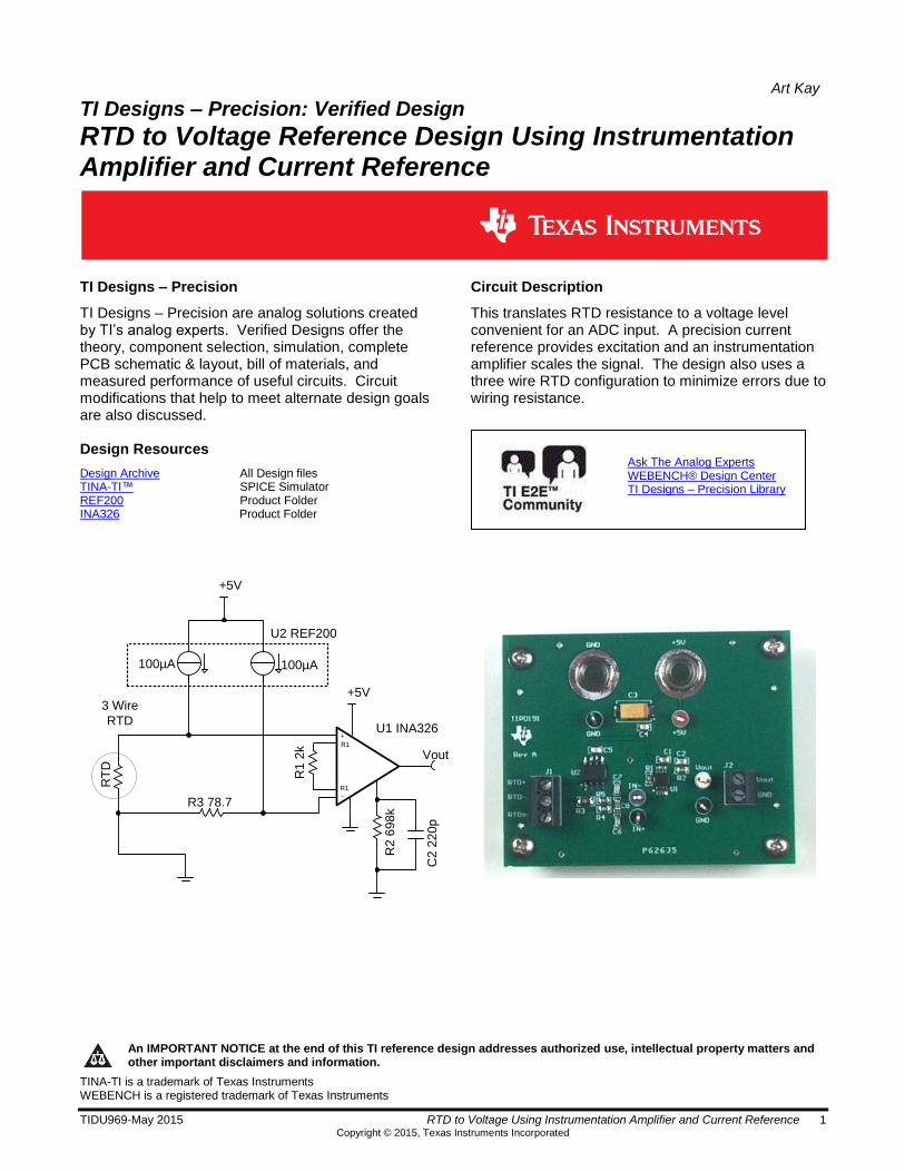
1 Design Summary
The design requirements are as follows:
Supply Voltage: 5 V
RTD temperature range: -50 to 125
RTD resistance range 80.3Ω to 147.9 Ω
Output: 0.1V to 4.9V
The design goals and performance are summarized in Table 1. Figure 1 depicts the measured transfer function of the design.
Table 1. Comparison of Design Goals, Calculations, Simulation, and Measured Performance
RTD Goal Calculated Simulated Measured
Vout (Max scale) 80.3Ω 0.1V 0.112V 0.117V 0.113V
Vout (Min scale) 142.9Ω 4.9V 4.83V 4.82V 4.862V
Figure 1: Measured Transfer Function
00.5
1
1.5
2
2.5
3
3.5
4
4.5
5
80 90 100 110 120 130 140 150
Vo
ut
(V)
RTD Resistance
Vout vs. RTD Resistance
www.ti.com
TIDU969-May 2015 RTD to Voltage Using Instrumentation Amplifier and Current Reference 3 Copyright © 2015, Texas Instruments Incorporated
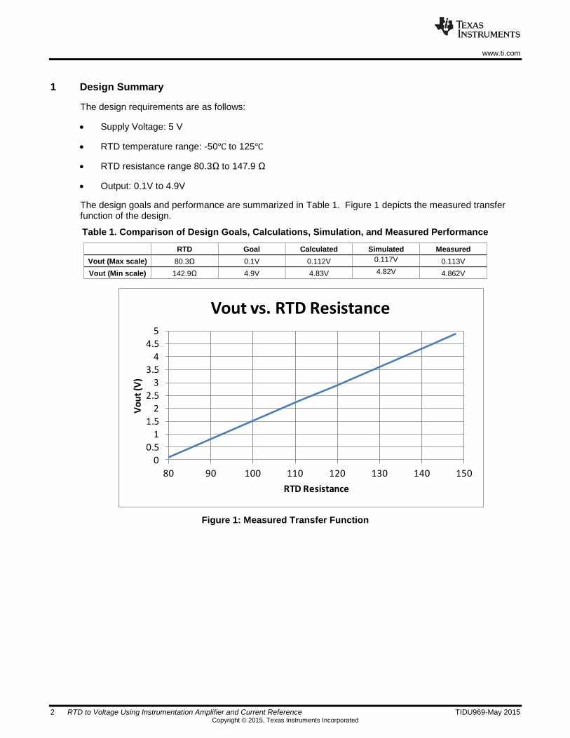
2 Theory of Operation
Figure 2 and Figure 3 show the schematic of the RTD amplifier for minimum and maximum output
conditions. Note that this circuit was designed for a -50 to 150 RTD temperature range. At -50 the RTD resistance is 80.3Ω and the voltage across it is 8.03mV (VRTD = (100µA)(80.3Ω), see Figure 2). Notice that R3 develops a voltage drop that opposes the RTD drop. The drop across R3 is used to shift amplifiers input differential voltage to a minimum level. The output is the differential input multiplied by the
gain (Vout = 698 ∙ 160µV = 0.111V). At 150 the RTD resistance is 148Ω and the voltage across it is 14.8mV (VRTD = (100µA)(148Ω)). This produces a differential input of 6.93mV and an output voltage of 4.84V (Vout = 698 ∙ 6.93mV = 4.84V, see Figure 3).
Figure 2: RTD Amplifier with Minimum Output Condition
Figure 3: RTD Amplifier with Maximum Output Condition
+5V
+5V
R1
2k
100µA
Vout
RT
D
+
-R1
R1
U1 INA326
R2
69
8k
C2
22
0p
R3 78.7
U2 REF200
3 Wire
RTD
200µA
- 7.87mV +
80.3Ω @
-50C
+
8.03mV
-
+
160µ V
-
0.111V
100µA
G = 2(R2/R1)
+5V
+5V
R1
2k
100µA
Vout
RT
D
+
-R1
R1
U1 INA326
R2
69
8k
C2
22
0p
R3 78.7
U2 REF200
3 Wire
RTD
200µA
- 7.87mV +
148Ω @
150C
+
14.8mV
-
+
6.93mV
-
4.84V
100µA
G = 2(R2/R1)

www.ti.com
4 RTD to Voltage Using Instrumentation Amplifier and Current Reference TIDU969-May 2015 Copyright © 2015, Texas Instruments Incorporated
2.1 Lead Resistance Cancelation (3 wire RTD)
Figure 4 below shows the three wire RTD configuration can be used to cancel lead resistance. Note that the resistance in each lead must be equal to cancel the error. Also, the two current sources in the REF200 need to be equal. Notice that the voltage developed on the two top leads of the RTD are equal and opposite polarity so that the amplifiers input is only from the RTD voltage. In this example, the RTD drop is 14.8mV and the leads each have 1mV. Notice that the 1mV drops cancel. Finally, notice that the voltage on the 3
rd lead (2mV) creates a small shift in the common mode voltage. In some applications, a
larger resistor is intentionally added to shift the common mode voltage. However, the INA326 has a rail to rail common mode range, so it can accept common mode voltages near ground.
Figure 4: Three wire RTD configuration cancels lead resistance
2.2 Noise Calculation The input noise is dominated by the INA326 noise (33nV/rtHz). The simplified calculation below ignores the noise from the REF200 and the thermal noise of the resistors. The noise simulation includes reference and thermal noise.
( 1 )
( 2 )
( 3 )
+5V
+5V
R1
2k
100µA
Vout
RT
D
+
-R1
R1
U1 INA326
R2
69
8k
C2
22
0p
R3 78.7
U2 REF200
3 Wire
RTD
148Ω @
150C
+
14.8mV
-4.84V
100µA
10Ω
- 1mV +
10Ω
- 1mV +
10Ω
+ 2mV -
+
14.8mV
-
Large Lead R
PCB
300m

www.ti.com
TIDU969-May 2015 RTD to Voltage Using Instrumentation Amplifier and Current Reference 5 Copyright © 2015, Texas Instruments Incorporated
2.3 Input Filter
Because the RTD leads are long, they may develop large common mode noise signals. The filter shown in Figure 5 is useful in attenuating the common mode noise pickup. Details on this configuration are covered in the Analog Engineers Pocket Reference ( www.ti.com/analogrefguide ).
Figure 5: Common Mode and Differential Noise filter
( 4 )
( 5 )
+5V
+5V
R1
2k
100µA
Vout
RT
D
+
-R1
R1
U1 INA326
R2
69
8k
C2
22
0p
R3 78.7
U2 REF200
3 Wire
RTD
80.3Ω @
-50C
100µA
R5 10k
R4 10k
Long Leads Common
Mode noise Pickup
Attenuated noise signal
C6
1nF
C7
1nF
C8
10nF
www.ti.com
6 RTD to Voltage Using Instrumentation Amplifier and Current Reference TIDU969-May 2015 Copyright © 2015, Texas Instruments Incorporated
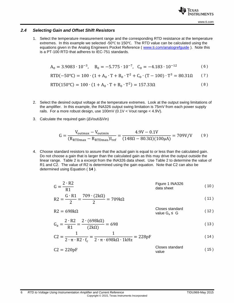
2.4 Selecting Gain and Offset Shift Resistors
1. Select the temperature measurement range and the corresponding RTD resistance at the temperature
extremes. In this example we selected -50 to 150. The RTD value can be calculated using the equations given in the Analog Engineers Pocket Reference ( www.ti.com/analogrefguide ). Note this is a PT-100 RTD that adheres to IEC-751 standards.
( 6 )
( 7 )
( 8 )
2. Select the desired output voltage at the temperature extremes. Look at the output swing limitations of the amplifier. In this example, the INA326 output swing limitation is 75mV from each power supply rails. For a more robust design, use 100mV (0.1V < Vout range < 4.9V).
3. Calculate the required gain (ΔVout/ΔVin)
( 9 )
4. Choose standard resistors to assure that the actual gain is equal to or less than the calculated gain. Do not choose a gain that is larger than the calculated gain as this may drive the output outside the linear range. Table 2 is a excerpt from the INA326 data sheet. Use Table 2 to determine the value of R1 and C2. The value of R2 is determined using the gain equation. Note that C2 can also be determined using Equation ( 14 ).
Figure 1 INA326 data sheet
( 10 )
( 11 )
Closes standard value Ga ≤ G
( 12 )
( 13 )
( 14 )
Closes standard value
( 15 )
www.ti.com
TIDU969-May 2015 RTD to Voltage Using Instrumentation Amplifier and Current Reference 7 Copyright © 2015, Texas Instruments Incorporated
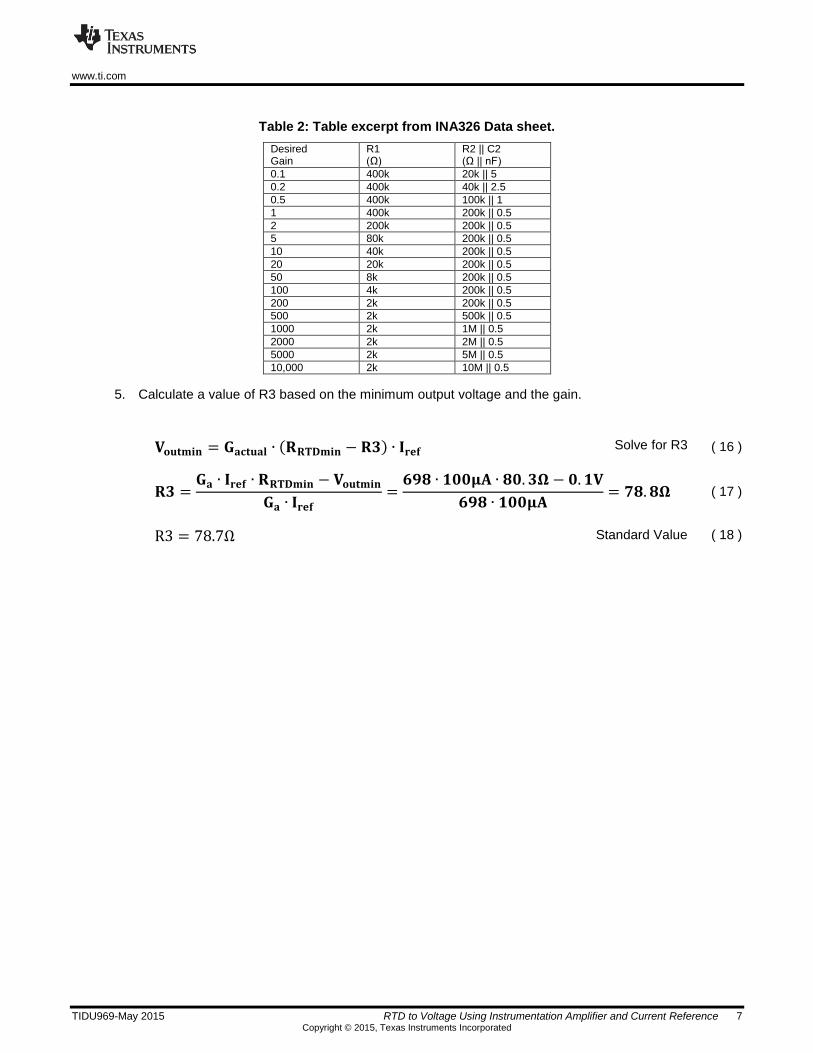
Table 2: Table excerpt from INA326 Data sheet.
Desired Gain
R1 (Ω)
R2 || C2 (Ω || nF)
0.1 400k 20k || 5
0.2 400k 40k || 2.5
0.5 400k 100k || 1
1 400k 200k || 0.5
2 200k 200k || 0.5
5 80k 200k || 0.5
10 40k 200k || 0.5
20 20k 200k || 0.5
50 8k 200k || 0.5
100 4k 200k || 0.5
200 2k 200k || 0.5
500 2k 500k || 0.5
1000 2k 1M || 0.5
2000 2k 2M || 0.5
5000 2k 5M || 0.5
10,000 2k 10M || 0.5
5. Calculate a value of R3 based on the minimum output voltage and the gain.
Solve for R3 ( 16 )
( 17 )
Standard Value ( 18 )

www.ti.com
8 RTD to Voltage Using Instrumentation Amplifier and Current Reference TIDU969-May 2015 Copyright © 2015, Texas Instruments Incorporated
3 Component Selection
3.1 Current Reference
The REF200 was because it is a convenient and simple way to generate a matched current source. The current setting of 100µA will work well for PT-100 and PT-1000 RTDs.
3.2 Passive Components
This design uses 1% thin film resistors and X7R ceramic capacitors. Special low distortion capacitors are not required in this application as the desired signal is dc.
www.ti.com
TIDU969-May 2015 RTD to Voltage Using Instrumentation Amplifier and Current Reference 9 Copyright © 2015, Texas Instruments Incorporated
4 Simulation
4.1 Transfer Function
The upper end points (temperature extremes) dc operating values were verified in simulation. The circuit below shows the simulation for the -50C point (80.3Ω). Note that the value of the RTD was manually adjusted to the appropriate value to test the condition. Table 3 shows the results for this simulation. Note that the ability of the three wire RTD configuration to reject lead resistance was also tested in simulation.
+5V
+5V
+5V
R1 2k
IS1 100uIS2 100u
V3 5
Vout
R_lead1 10
R_Lead2 10
RT
D 8
0.3 V
+
VM1
V+
VM2
Vcm
++
-R1
R1
R2
U3 INA326T
R2 6
98k
C2 5
00p
R_Lead3 10
R3 78.7
V+
VM3
RTD = 80.3 -> -50C
RTD = 147.94 -> 125C
8.03mV
2mV
8.03mV
160uV
117.15mV
Figure 6: Frequency response for OPA376 ac coupled amplifier
Table 3: DC Output for RTD Resistance
Temperature RTD Value Output (0Ω line R) Output (10Ω line R)
-50 80.3Ω 0.117V 0.117V
150 149.94Ω 4.82V 4.82V
Note: All lead resistances are equal (R_lead1 = R_lead2 = R_lead3)
www.ti.com
10 RTD to Voltage Using Instrumentation Amplifier and Current Reference TIDU969-May 2015 Copyright © 2015, Texas Instruments Incorporated
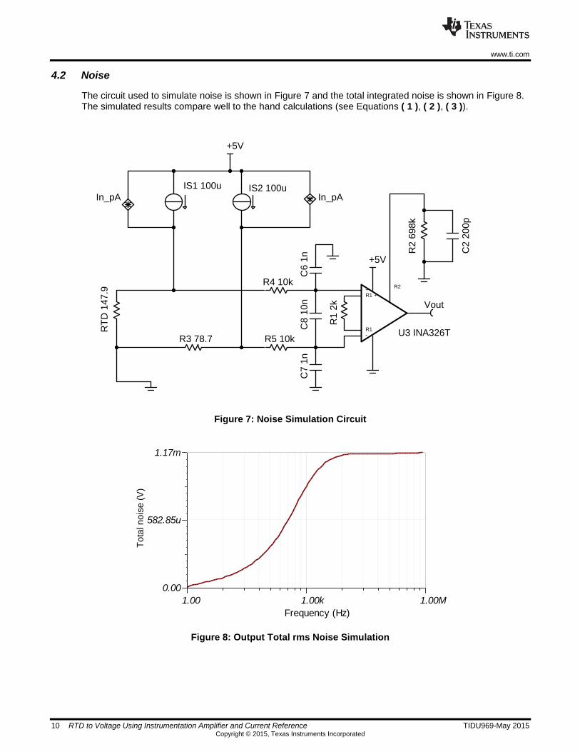
4.2 Noise
The circuit used to simulate noise is shown in Figure 7 and the total integrated noise is shown in Figure 8. The simulated results compare well to the hand calculations (see Equations ( 1 ), ( 2 ), ( 3 )).
+5V
+5V
R1
2k
IS1 100u IS2 100u
Vout
RT
D 1
47
.9 ++
-R1
R1
R2
U3 INA326T
R2
69
8k
C2
20
0p
R3 78.7
R4 10k
R5 10k
In_pA In_pA
C8
10
nC
6 1
nC
7 1
n
Figure 7: Noise Simulation Circuit
Figure 8: Output Total rms Noise Simulation
T
Frequency (Hz)
1.00 1.00k 1.00M
To
tal n
ois
e (
V)
0.00
582.85u
1.17m

www.ti.com
TIDU969-May 2015 RTD to Voltage Using Instrumentation Amplifier and Current Reference 11 Copyright © 2015, Texas Instruments Incorporated
5 PCB Design
The PCB schematic and bill of materials can be found in the Appendix.
5.1 PCB Layout
Normal PCB layout precautions were in this layout (i.e. short traces, solid ground connections, minimized vias, close decoupling capacitors).
Figure 9: PCB Layout (Top - Red, Bottom - Blue)
www.ti.com
12 RTD to Voltage Using Instrumentation Amplifier and Current Reference TIDU969-May 2015 Copyright © 2015, Texas Instruments Incorporated
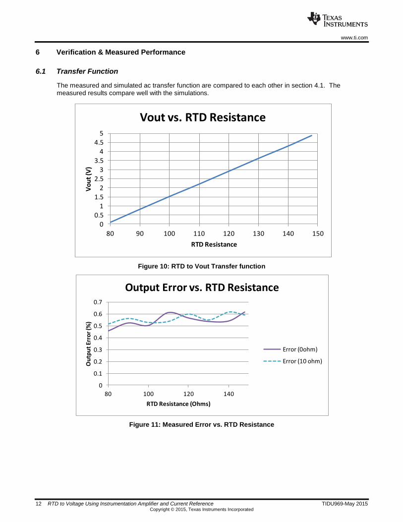
6 Verification & Measured Performance
6.1 Transfer Function
The measured and simulated ac transfer function are compared to each other in section 4.1. The measured results compare well with the simulations.
Figure 10: RTD to Vout Transfer function
Figure 11: Measured Error vs. RTD Resistance
00.5
1
1.5
2
2.5
3
3.5
4
4.5
5
80 90 100 110 120 130 140 150
Vo
ut
(V)
RTD Resistance
Vout vs. RTD Resistance
0
0.1
0.2
0.3
0.4
0.5
0.6
0.7
80 100 120 140
Ou
tpu
t Er
ror
(%)
RTD Resistance (Ohms)
Output Error vs. RTD Resistance
Error (0ohm)
Error (10 ohm)

www.ti.com
TIDU969-May 2015 RTD to Voltage Using Instrumentation Amplifier and Current Reference 13 Copyright © 2015, Texas Instruments Incorporated
6.2 Noise Measurement
The measured noise results are shown in Figure 12. Note that the unfiltered noise is significantly higher than the calculated noise calculate and simulated earlier and the filtered is slightly higher. The previous calculations assumed a 1kHz low pass filter which was not included on the PCB design. Note that the noise contains auto-zero switching noise.
Unfiltered
Output
1kHz
Filtered
Output
Figure 12: Measured Noise
Figure 13: External 1.6kHz Low Pass Filter
+5V
+5V
R1
2k
100µA
Vout
RT
D
+
-R1
R1
U1 INA326
R2
69
8k
C2
22
0p
R3 78.7
U2 REF200
3 Wire
RTD
80.3Ω @
-50C
100µA
100Ω
1µF
External 1.6kHz
Low Pass Filter
www.ti.com
14 RTD to Voltage Using Instrumentation Amplifier and Current Reference TIDU969-May 2015 Copyright © 2015, Texas Instruments Incorporated
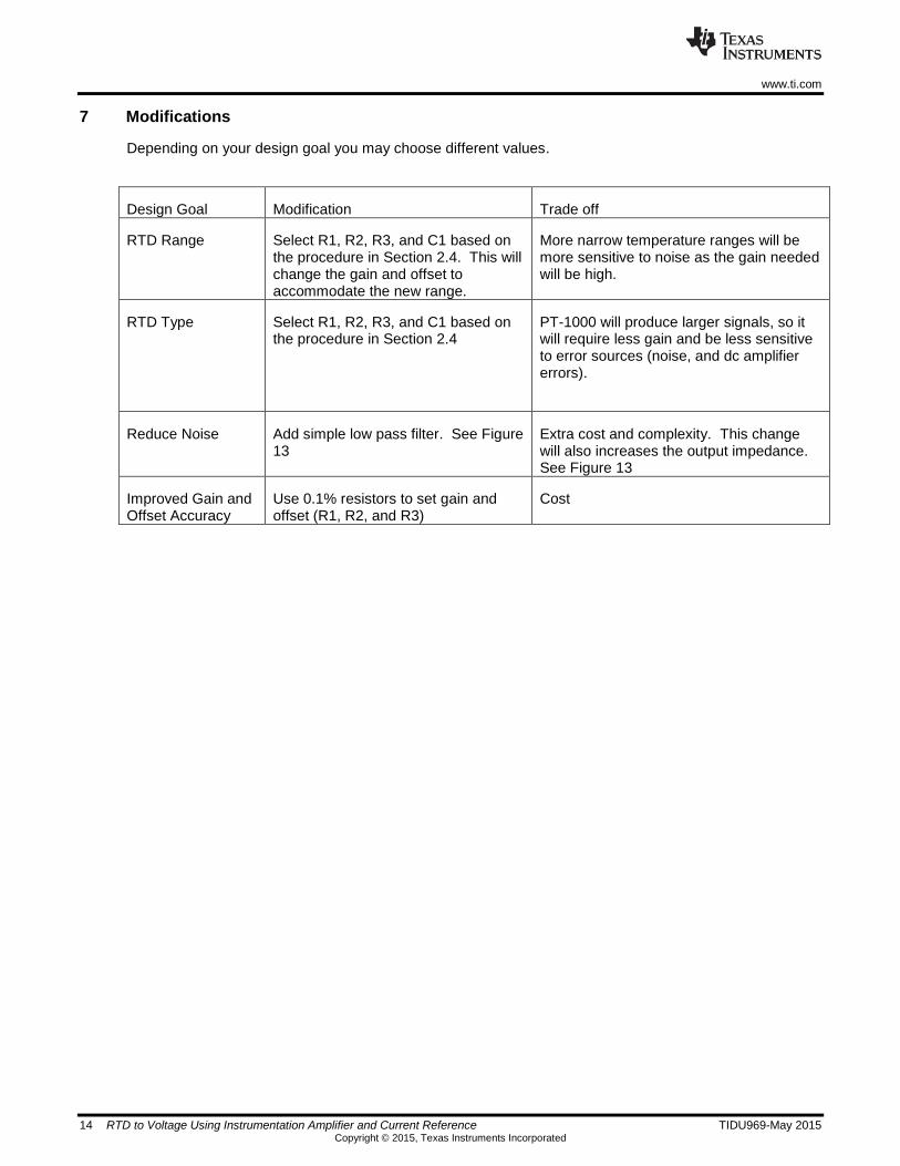
7 Modifications
Depending on your design goal you may choose different values.
Design Goal Modification Trade off
RTD Range Select R1, R2, R3, and C1 based on the procedure in Section 2.4. This will change the gain and offset to accommodate the new range.
More narrow temperature ranges will be more sensitive to noise as the gain needed will be high.
RTD Type Select R1, R2, R3, and C1 based on the procedure in Section 2.4
PT-1000 will produce larger signals, so it will require less gain and be less sensitive to error sources (noise, and dc amplifier errors).
Reduce Noise Add simple low pass filter. See Figure 13
Extra cost and complexity. This change will also increases the output impedance. See Figure 13
Improved Gain and Offset Accuracy
Use 0.1% resistors to set gain and offset (R1, R2, and R3)
Cost

www.ti.com
TIDU969-May 2015 RTD to Voltage Using Instrumentation Amplifier and Current Reference 15 Copyright © 2015, Texas Instruments Incorporated
8 About the Author
Arthur Kay is an applications engineering manager at TI where he specializes in the support of amplifiers, references, and mixed signal devices. Arthur focuses a good deal on industrial applications such as bridge sensor signal conditioning. Arthur has published a book and an article series on amplifier noise. Arthur received his M.S.E.E. from Georgia Institute of Technology, and B.S.E.E. from Cleveland State University.
9 Acknowledgements & References
1. A. Kay, Operational Amplifier Noise: Techniques and Tips for Analyzing and Reducing Noise. Elsevier, 2012.
2. A. Kay and T. Green. (2012, February 8). Analog Engineer’s Pocket Reference. Available: www.ti.com/analogrefguide
www.ti.com
16 RTD to Voltage Using Instrumentation Amplifier and Current Reference TIDU969-May 2015 Copyright © 2015, Texas Instruments Incorporated
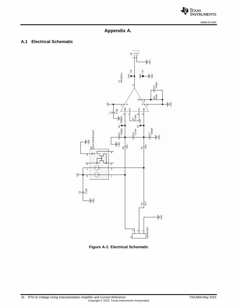
Appendix A.
A.1 Electrical Schematic
Figure A-1: Electrical Schematic
www.ti.com
TIDU969-May 2015 RTD to Voltage Using Instrumentation Amplifier and Current Reference 17 Copyright © 2015, Texas Instruments Incorporated
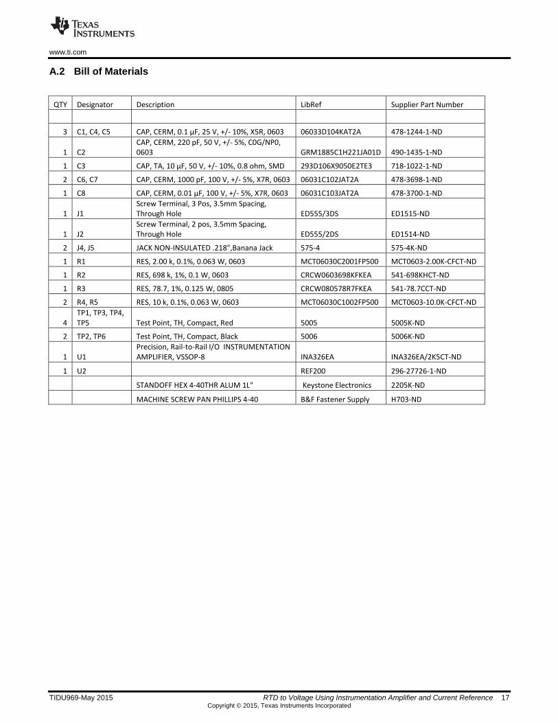
A.2 Bill of Materials
QTY Designator Description LibRef Supplier Part Number
3 C1, C4, C5 CAP, CERM, 0.1 µF, 25 V, +/- 10%, X5R, 0603 06033D104KAT2A 478-1244-1-ND
1 C2 CAP, CERM, 220 pF, 50 V, +/- 5%, C0G/NP0, 0603 GRM1885C1H221JA01D 490-1435-1-ND
1 C3 CAP, TA, 10 µF, 50 V, +/- 10%, 0.8 ohm, SMD 293D106X9050E2TE3 718-1022-1-ND
2 C6, C7 CAP, CERM, 1000 pF, 100 V, +/- 5%, X7R, 0603 06031C102JAT2A 478-3698-1-ND
1 C8 CAP, CERM, 0.01 µF, 100 V, +/- 5%, X7R, 0603 06031C103JAT2A 478-3700-1-ND
1 J1 Screw Terminal, 3 Pos, 3.5mm Spacing, Through Hole ED555/3DS ED1515-ND
1 J2 Screw Terminal, 2 pos, 3.5mm Spacing, Through Hole ED555/2DS ED1514-ND
2 J4, J5 JACK NON-INSULATED .218",Banana Jack 575-4 575-4K-ND
1 R1 RES, 2.00 k, 0.1%, 0.063 W, 0603 MCT06030C2001FP500 MCT0603-2.00K-CFCT-ND
1 R2 RES, 698 k, 1%, 0.1 W, 0603 CRCW0603698KFKEA 541-698KHCT-ND
1 R3 RES, 78.7, 1%, 0.125 W, 0805 CRCW080578R7FKEA 541-78.7CCT-ND
2 R4, R5 RES, 10 k, 0.1%, 0.063 W, 0603 MCT06030C1002FP500 MCT0603-10.0K-CFCT-ND
4 TP1, TP3, TP4, TP5 Test Point, TH, Compact, Red 5005 5005K-ND
2 TP2, TP6 Test Point, TH, Compact, Black 5006 5006K-ND
1 U1 Precision, Rail-to-Rail I/O INSTRUMENTATION AMPLIFIER, VSSOP-8 INA326EA INA326EA/2K5CT-ND
1 U2
REF200 296-27726-1-ND
STANDOFF HEX 4-40THR ALUM 1L" Keystone Electronics 2205K-ND
MACHINE SCREW PAN PHILLIPS 4-40 B&F Fastener Supply H703-ND

IMPORTANT NOTICE FOR TI REFERENCE DESIGNS
Texas Instruments Incorporated ("TI") reference designs are solely intended to assist designers (“Buyers”) who are developing systems thatincorporate TI semiconductor products (also referred to herein as “components”). Buyer understands and agrees that Buyer remainsresponsible for using its independent analysis, evaluation and judgment in designing Buyer’s systems and products.TI reference designs have been created using standard laboratory conditions and engineering practices. TI has not conducted anytesting other than that specifically described in the published documentation for a particular reference design. TI may makecorrections, enhancements, improvements and other changes to its reference designs.Buyers are authorized to use TI reference designs with the TI component(s) identified in each particular reference design and to modify thereference design in the development of their end products. HOWEVER, NO OTHER LICENSE, EXPRESS OR IMPLIED, BY ESTOPPELOR OTHERWISE TO ANY OTHER TI INTELLECTUAL PROPERTY RIGHT, AND NO LICENSE TO ANY THIRD PARTY TECHNOLOGYOR INTELLECTUAL PROPERTY RIGHT, IS GRANTED HEREIN, including but not limited to any patent right, copyright, mask work right,or other intellectual property right relating to any combination, machine, or process in which TI components or services are used.Information published by TI regarding third-party products or services does not constitute a license to use such products or services, or awarranty or endorsement thereof. Use of such information may require a license from a third party under the patents or other intellectualproperty of the third party, or a license from TI under the patents or other intellectual property of TI.TI REFERENCE DESIGNS ARE PROVIDED "AS IS". TI MAKES NO WARRANTIES OR REPRESENTATIONS WITH REGARD TO THEREFERENCE DESIGNS OR USE OF THE REFERENCE DESIGNS, EXPRESS, IMPLIED OR STATUTORY, INCLUDING ACCURACY ORCOMPLETENESS. TI DISCLAIMS ANY WARRANTY OF TITLE AND ANY IMPLIED WARRANTIES OF MERCHANTABILITY, FITNESSFOR A PARTICULAR PURPOSE, QUIET ENJOYMENT, QUIET POSSESSION, AND NON-INFRINGEMENT OF ANY THIRD PARTYINTELLECTUAL PROPERTY RIGHTS WITH REGARD TO TI REFERENCE DESIGNS OR USE THEREOF. TI SHALL NOT BE LIABLEFOR AND SHALL NOT DEFEND OR INDEMNIFY BUYERS AGAINST ANY THIRD PARTY INFRINGEMENT CLAIM THAT RELATES TOOR IS BASED ON A COMBINATION OF COMPONENTS PROVIDED IN A TI REFERENCE DESIGN. IN NO EVENT SHALL TI BELIABLE FOR ANY ACTUAL, SPECIAL, INCIDENTAL, CONSEQUENTIAL OR INDIRECT DAMAGES, HOWEVER CAUSED, ON ANYTHEORY OF LIABILITY AND WHETHER OR NOT TI HAS BEEN ADVISED OF THE POSSIBILITY OF SUCH DAMAGES, ARISING INANY WAY OUT OF TI REFERENCE DESIGNS OR BUYER’S USE OF TI REFERENCE DESIGNS.TI reserves the right to make corrections, enhancements, improvements and other changes to its semiconductor products and services perJESD46, latest issue, and to discontinue any product or service per JESD48, latest issue. Buyers should obtain the latest relevantinformation before placing orders and should verify that such information is current and complete. All semiconductor products are soldsubject to TI’s terms and conditions of sale supplied at the time of order acknowledgment.TI warrants performance of its components to the specifications applicable at the time of sale, in accordance with the warranty in TI’s termsand conditions of sale of semiconductor products. Testing and other quality control techniques for TI components are used to the extent TIdeems necessary to support this warranty. Except where mandated by applicable law, testing of all parameters of each component is notnecessarily performed.TI assumes no liability for applications assistance or the design of Buyers’ products. Buyers are responsible for their products andapplications using TI components. To minimize the risks associated with Buyers’ products and applications, Buyers should provideadequate design and operating safeguards.Reproduction of significant portions of TI information in TI data books, data sheets or reference designs is permissible only if reproduction iswithout alteration and is accompanied by all associated warranties, conditions, limitations, and notices. TI is not responsible or liable forsuch altered documentation. Information of third parties may be subject to additional restrictions.Buyer acknowledges and agrees that it is solely responsible for compliance with all legal, regulatory and safety-related requirementsconcerning its products, and any use of TI components in its applications, notwithstanding any applications-related information or supportthat may be provided by TI. Buyer represents and agrees that it has all the necessary expertise to create and implement safeguards thatanticipate dangerous failures, monitor failures and their consequences, lessen the likelihood of dangerous failures and take appropriateremedial actions. Buyer will fully indemnify TI and its representatives against any damages arising out of the use of any TI components inBuyer’s safety-critical applications.In some cases, TI components may be promoted specifically to facilitate safety-related applications. With such components, TI’s goal is tohelp enable customers to design and create their own end-product solutions that meet applicable functional safety standards andrequirements. Nonetheless, such components are subject to these terms.No TI components are authorized for use in FDA Class III (or similar life-critical medical equipment) unless authorized officers of the partieshave executed an agreement specifically governing such use.Only those TI components that TI has specifically designated as military grade or “enhanced plastic” are designed and intended for use inmilitary/aerospace applications or environments. Buyer acknowledges and agrees that any military or aerospace use of TI components thathave not been so designated is solely at Buyer's risk, and Buyer is solely responsible for compliance with all legal and regulatoryrequirements in connection with such use.TI has specifically designated certain components as meeting ISO/TS16949 requirements, mainly for automotive use. In any case of use ofnon-designated products, TI will not be responsible for any failure to meet ISO/TS16949.IMPORTANT NOTICE
Mailing Address: Texas Instruments, Post Office Box 655303, Dallas, Texas 75265Copyright © 2015, Texas Instruments Incorporated
Related Documents