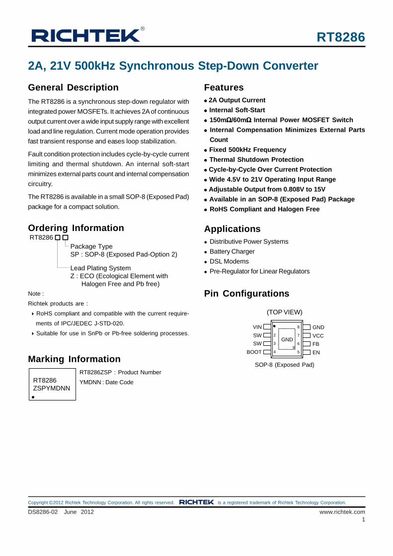
RT8286 ® DS8286-02 June 2012 www.richtek.com 1 © Copyright 2012 Richtek Technology Corporation. All rights reserved. is a registered trademark of Richtek Technology Corporation. Ordering Information Note : Richtek products are : RoHS compliant and compatible with the current require- ments of IPC/JEDEC J-STD-020. Suitable for use in SnPb or Pb-free soldering processes. Applications Distributive Power Systems Battery Charger DSL Modems Pre-Regulator for Linear Regulators Pin Configurations General Description The RT8286 is a synchronous step-down regulator with integrated power MOSFETs. It achieves 2A of continuous output current over a wide input supply range with excellent load and line regulation. Current mode operation provides fast transient response and eases loop stabilization. Fault condition protection includes cycle-by-cycle current limiting and thermal shutdown. An internal soft-start minimizes external parts count and internal compensation circuitry. The RT8286 is available in a small SOP-8 (Exposed Pad) package for a compact solution. Features 2A Output Current Internal Soft-Start 150mΩ/60mΩ Ω Ω Ω Ω Internal Power MOSFET Switch Internal Compensation Minimizes External Parts Count Fixed 500kHz Frequency Thermal Shutdown Protection Cycle-by-Cycle Over Current Protection Wide 4.5V to 21V Operating Input Range Adjustable Output from 0.808V to 15V Available in an SOP-8 (Exposed Pad) Package RoHS Compliant and Halogen Free SOP-8 (Exposed Pad) (TOP VIEW) Marking Information RT8286ZSP : Product Number YMDNN : Date Code 2A, 21V 500kHz Synchronous Step-Down Converter Package Type SP : SOP-8 (Exposed Pad-Option 2) RT8286 Lead Plating System Z : ECO (Ecological Element with Halogen Free and Pb free) RT8286 ZSPYMDNN VIN SW SW BOOT GND VCC EN FB GND 2 3 4 5 6 7 8 9

Welcome message from author
This document is posted to help you gain knowledge. Please leave a comment to let me know what you think about it! Share it to your friends and learn new things together.
Transcript
RT8286®
DS8286-02 June 2012 www.richtek.com1
©Copyright 2012 Richtek Technology Corporation. All rights reserved. is a registered trademark of Richtek Technology Corporation.
Ordering Information
Note :
Richtek products are :
RoHS compliant and compatible with the current require-
ments of IPC/JEDEC J-STD-020.
Suitable for use in SnPb or Pb-free soldering processes.
ApplicationsDistributive Power SystemsBattery ChargerDSL ModemsPre-Regulator for Linear Regulators
Pin Configurations
General DescriptionThe RT8286 is a synchronous step-down regulator withintegrated power MOSFETs. It achieves 2A of continuousoutput current over a wide input supply range with excellentload and line regulation. Current mode operation providesfast transient response and eases loop stabilization.
Fault condition protection includes cycle-by-cycle currentlimiting and thermal shutdown. An internal soft-startminimizes external parts count and internal compensationcircuitry.
The RT8286 is available in a small SOP-8 (Exposed Pad)package for a compact solution.
Features 2A Output Current Internal Soft-Start 150mΩΩΩΩΩ/60mΩ Ω Ω Ω Ω Internal Power MOSFET Switch Internal Compensation Minimizes External PartsCount
Fixed 500kHz Frequency Thermal Shutdown Protection Cycle-by-Cycle Over Current Protection Wide 4.5V to 21V Operating Input Range Adjustable Output from 0.808V to 15V Available in an SOP-8 (Exposed Pad) PackageRoHS Compliant and Halogen Free
SOP-8 (Exposed Pad)
(TOP VIEW)
Marking InformationRT8286ZSP : Product Number
YMDNN : Date Code
2A, 21V 500kHz Synchronous Step-Down Converter
Package TypeSP : SOP-8 (Exposed Pad-Option 2)
RT8286
Lead Plating SystemZ : ECO (Ecological Element with Halogen Free and Pb free)
RT8286ZSPYMDNN
VINSWSW
BOOT
GNDVCC
ENFB
GND2
3
4 5
6
7
8
9

RT8286
2DS8286-02 June 2012www.richtek.com
©Copyright 2012 Richtek Technology Corporation. All rights reserved. is a registered trademark of Richtek Technology Corporation.
Functional Pin DescriptionPin No. Pin Name Pin Function
1 VIN Supply Input. VIN supplies the power to the IC, as well as the step-down converter switches. Drive VIN with a 4.5V to 21V power source. Bypass VIN to GND with a suitably large capacitor to eliminate noise on the input to the IC.
2, 3 SW Switch Node. SW is the switching node that supplies power to the output. Connect the output LC filter from SW to the output load. Note that a capacitor is required from SW to BOOT to power the high side switch.
4 BOOT High Side Gate Drive Boost Input. BOOT supplies the drive for the high side N-MOSFET switch. Connect a 100nF or greater capacitor from SW to BOOT to power the high side switch.
5 EN Chip Enable (Active High). For automatic start up, connect the EN pin to VIN with a 100kΩ resistor.
6 FB Feedback Input. FB senses the output voltage to regulate said voltage. Drive FB with a resistive voltage divider from the output voltage. The feedback threshold is 0.808V.
7 VCC Bias Supply. Decouple with 0.1μF to 0.22μF capacitor. The capacitance should be no more than 0.22μF.
8, 9 (Exposed Pad) GND Ground. The Exposed Pad must be soldered to a large PCB and connected to
GND for maximum power dissipation.
Typical Application Circuit
Table 1. Recommended Components SelectionVOUT (V) R1 (kΩ) R2 (kΩ) RT (kΩ) L (μH) COUT (μF)
5 75 14.46 0 4.7 22 x 2 3.3 75 24.32 0 3.6 22 x 2 2.5 75 35.82 0 3.6 22 x 2 1.8 5 4.07 30 2 22 x 2 1.5 5 5.84 39 2 22 x 2 1.2 5 10.31 47 2 22 x 2 1.05 5 16.69 47 1.5 22 x 2
VIN
EN
GND
BOOT
FB
SW5 6
1
2, 3
4
L100nF
R2
22µF RT8286
8, 9 (Exposed Pad)
CBOOT
RT
CIN
COUTR1
VCC
0.1µFCC
7
VIN
VOUTChip Enable
RT8286
3DS8286-02 June 2012 www.richtek.com
©Copyright 2012 Richtek Technology Corporation. All rights reserved. is a registered trademark of Richtek Technology Corporation.
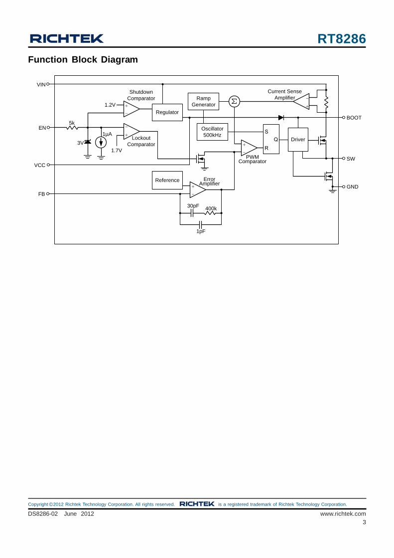
Function Block Diagram
SQ
RDriver
-
+
Current Sense Amplifier
PWM Comparator
Oscillator500kHz
Ramp Generator
Regulator
Reference+
-
Error Amplifier
SW
BOOT
FB
EN
VIN
+
-
GND
VCC
+
-
1.2V
+
-
1.7V
1µA
3V
5k
Lockout Comparator
Shutdown Comparator
400k30pF
1pF

RT8286
4DS8286-02 June 2012www.richtek.com
©Copyright 2012 Richtek Technology Corporation. All rights reserved. is a registered trademark of Richtek Technology Corporation.
Absolute Maximum Ratings (Note 1)
Supply Voltage, VIN ------------------------------------------------------------------------------------------- −0.3V to 26VSwitch Voltage, SW ------------------------------------------------------------------------------------------- −0.3V to (VIN + 0.3V)Boot Voltage, BOOT ------------------------------------------------------------------------------------------- (SW − 0.3V) to (SW + 6V)Other Pins-------------------------------------------------------------------------------------------------------- −0.3V to 6VPower Dissipation, PD @ TA = 25°CSOP-8 (Exposed Pad) ---------------------------------------------------------------------------------------- 1.333WPackage Thermal Resistance (Note 2)SOP-8 (Exposed Pad), θJA ----------------------------------------------------------------------------------- 75°C/W
SOP-8 (Exposed Pad), θJC ---------------------------------------------------------------------------------------------------------------------- 15°C/WJunction Temperature ------------------------------------------------------------------------------------------ 150°CLead Temperature (Soldering, 10 sec.) -------------------------------------------------------------------- 260°CStorage Temperature Range --------------------------------------------------------------------------------- −65°C to 150°CESD Susceptibility (Note 3)HBM (Human Body Model) ----------------------------------------------------------------------------------- 2kV
Recommended Operating Conditions (Note 4)
Supply Input Voltage Range, VIN --------------------------------------------------------------------------- 4.5V to 21VJunction Temperature Range--------------------------------------------------------------------------------- −40°C to 125°CAmbient Temperature Range--------------------------------------------------------------------------------- −40°C to 85°C
Electrical Characteristics (VIN = 5V, TA = 25°C, unless otherwise specified)
Parameter Symbol Test Conditions Min Typ Max Unit Shutdown Current ISHDN VEN = 0 -- 0 1 μA Quiescent Current IQ VEN = 2V, VFB = 1V -- 0.7 -- mA Upper Switch On Resistance RDS(ON)1 -- 150 -- mΩ Lower Switch On Resistance RDS(ON)2 -- 60 -- mΩ Switch Leakage ILEAK VEN = 0V, VSW = 0V or 12V -- 0 10 μA Current Limit ILIM VBOOT − VSW = 4.8V 3.9 5 -- A Oscillator Frequency fSW VFB = 0.75V 425 500 575 kHz Short Circuit Frequency VFB = 0V -- 150 -- kHz Maximum Duty Cycle DMAX VFB = 0.8V -- 90 -- % Minimum On Time tON -- 100 -- ns Feedback Voltage VFB 4.5V ≤ VIN ≤ 21V 0.796 0.808 0.82 V Feedback Current IFB -- 10 50 nA
Logic-High VIH 2 -- 5.5 EN Input Threshold Voltage Logic-Low VIL -- -- 0.4
V
VEN = 2V -- 1 -- Enable Current
VEN = 0V -- 0 -- μA
Under Voltage Lockout Threshold VUVLO VIN Rising 3.8 4 4.2 V Under Voltage Lockout Threshold Hysteresis ΔVUVLO -- 400 -- mV
RT8286
5DS8286-02 June 2012 www.richtek.com
©Copyright 2012 Richtek Technology Corporation. All rights reserved. is a registered trademark of Richtek Technology Corporation.
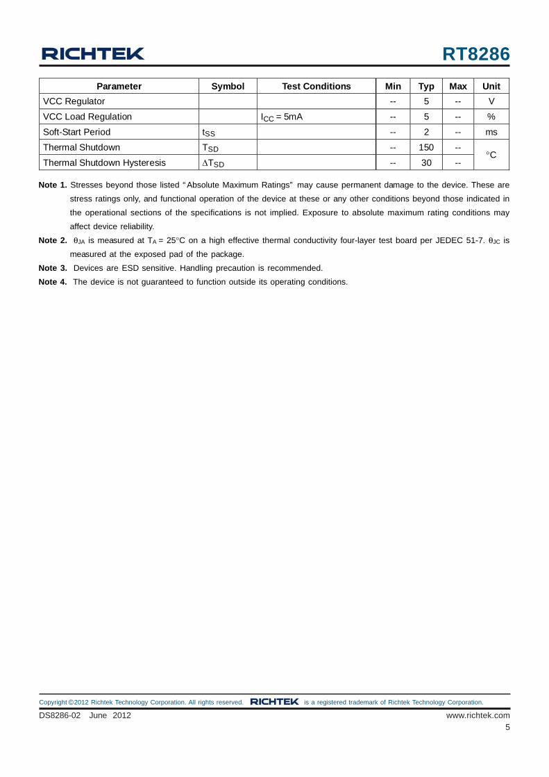
Parameter Symbol Test Conditions Min Typ Max Unit VCC Regulator -- 5 -- V
VCC Load Regulation ICC = 5mA -- 5 -- %
Soft-Start Period tSS -- 2 -- ms
Thermal Shutdown TSD -- 150 --
Thermal Shutdown Hysteresis ΔTSD -- 30 -- °C
Note 1. Stresses beyond those listed “Absolute Maximum Ratings” may cause permanent damage to the device. These are
stress ratings only, and functional operation of the device at these or any other conditions beyond those indicated in
the operational sections of the specifications is not implied. Exposure to absolute maximum rating conditions may
affect device reliability.
Note 2. θJA is measured at TA = 25°C on a high effective thermal conductivity four-layer test board per JEDEC 51-7. θJC is
measured at the exposed pad of the package.
Note 3. Devices are ESD sensitive. Handling precaution is recommended.
Note 4. The device is not guaranteed to function outside its operating conditions.

RT8286
6DS8286-02 June 2012www.richtek.com
©Copyright 2012 Richtek Technology Corporation. All rights reserved. is a registered trademark of Richtek Technology Corporation.
Output Voltage vs. Output Current
1.200
1.205
1.210
1.215
1.220
1.225
1.230
1.235
1.240
0 0.25 0.5 0.75 1 1.25 1.5 1.75 2
Output Current (A)
Out
put V
olta
ge (V
)
VIN = 12V, VOUT = 1.22V, IOUT = 0A to 2A
Reference Voltage vs. Input Voltage
0.790
0.795
0.800
0.805
0.810
0.815
0.820
0.825
0.830
4 6 8 10 12 14 16 18 20 22
Input Voltage (V)
Ref
eren
ce V
olta
ge (V
)Reference Voltage vs. Temperature
0.76
0.77
0.78
0.79
0.80
0.81
0.82
0.83
0.84
-50 -25 0 25 50 75 100 125
Temperature (°C)
Ref
eren
ce V
olta
ge (V
)
Typical Operating Characteristics
Efficiency vs. Output Current
0
10
20
30
40
50
60
70
80
90
100
0 0.25 0.5 0.75 1 1.25 1.5 1.75 2
Output Current (A)
Effi
cien
cy (%
)
VOUT = 1.22V, IOUT = 0A to 2A
VIN = 12V
VIN = 21V
Switching Frequency vs. Temperature
350
375
400
425
450
475
500
525
550
-50 -25 0 25 50 75 100 125
Temperature (°C)
Sw
itchi
ng F
requ
ency
(kH
z) 1
VIN = 12V, VOUT = 1.22V, IOUT = 1A
Switching Frequency vs. Input Voltage
350
375
400
425
450
475
500
525
550
4 6 8 10 12 14 16 18 20 22
Input Voltage (V)
Sw
itchi
ng F
requ
ency
(kH
z) 1
VOUT = 1.22V, IOUT = 0.8A

RT8286
7DS8286-02 June 2012 www.richtek.com
©Copyright 2012 Richtek Technology Corporation. All rights reserved. is a registered trademark of Richtek Technology Corporation.
Current Limit vs. Input Voltage
0
2
4
6
8
10
4 6 8 10 12 14 16 18 20 22
Input Voltage (V)
Cur
rent
Lim
it (A
)
Output Voltage Ripple
Time (1μs/Div)
IL(2A/Div)
VLX(10V/Div)
VIN = 12V, IOUT = 2A
VOUT(50mV/Div)
Output Voltage Ripple
Time (1μs/Div)
IL(2A/Div)
VLX(10V/Div)
VIN = 12V, IOUT = 1A
VOUT(50mV/Div)
VIN = 12V, VOUT = 1.22V, IOUT = 1A to 2A
Load Transient Response
Time (100μs/Div)
IOUT(1A/Div)
VOUT(200mV/Div)
VIN = 12V, VOUT = 1.22V, IOUT = 0A to 2A
Load Transient Response
Time (100μs/Div)
IOUT(1A/Div)
VOUT(200mV/Div)
Current Limit vs. Temperature
0
2
4
6
8
10
-50 -25 0 25 50 75 100 125
Temperature (°C)
Cur
rent
Lim
it (A
)
VIN = 12V, VOUT = 1.22V

RT8286
8DS8286-02 June 2012www.richtek.com
©Copyright 2012 Richtek Technology Corporation. All rights reserved. is a registered trademark of Richtek Technology Corporation.
Power Off from EN
Time (50μs/Div)
IL(2A/Div)
VOUT(1V/Div)
VEN(5V/Div)
VIN = 12V, VOUT = 1.22V, IOUT = 2A
VLX(10V/Div)
Power On from EN
Time (2.5ms/Div)
IL(2A/Div)
VOUT(1V/Div)
VEN(5V/Div)
VIN = 12V, VOUT = 1.22V, IOUT = 2A
VLX(10V/Div)
Power Off from VIN
Time (50ms/Div)
IL(2A/Div)
VOUT(1V/Div)
VIN(10V/Div)
VIN = 12V, VOUT = 1.22V, IOUT = 2A
Power On from VIN
Time (5ms/Div)
IL(2A/Div)
VOUT(1V/Div)
VIN(10V/Div)
VIN = 12V, VOUT = 1.22V, IOUT = 2A
RT8286
9DS8286-02 June 2012 www.richtek.com
©Copyright 2012 Richtek Technology Corporation. All rights reserved. is a registered trademark of Richtek Technology Corporation.
Application InformationThe IC is a synchronous high voltage buck converter thatcan support the input voltage range from 4.5V to 21V andthe output current can be up to 2A.
Output Voltage SettingThe output voltage is set by an external resistive divideraccording to the following equation :
where VFB is the feedback reference voltage 0.808V(typical).
The resistive divider allows the FB pin to sense a fractionof the output voltage as shown in Figure 1.
Figure 1. Output Voltage Setting
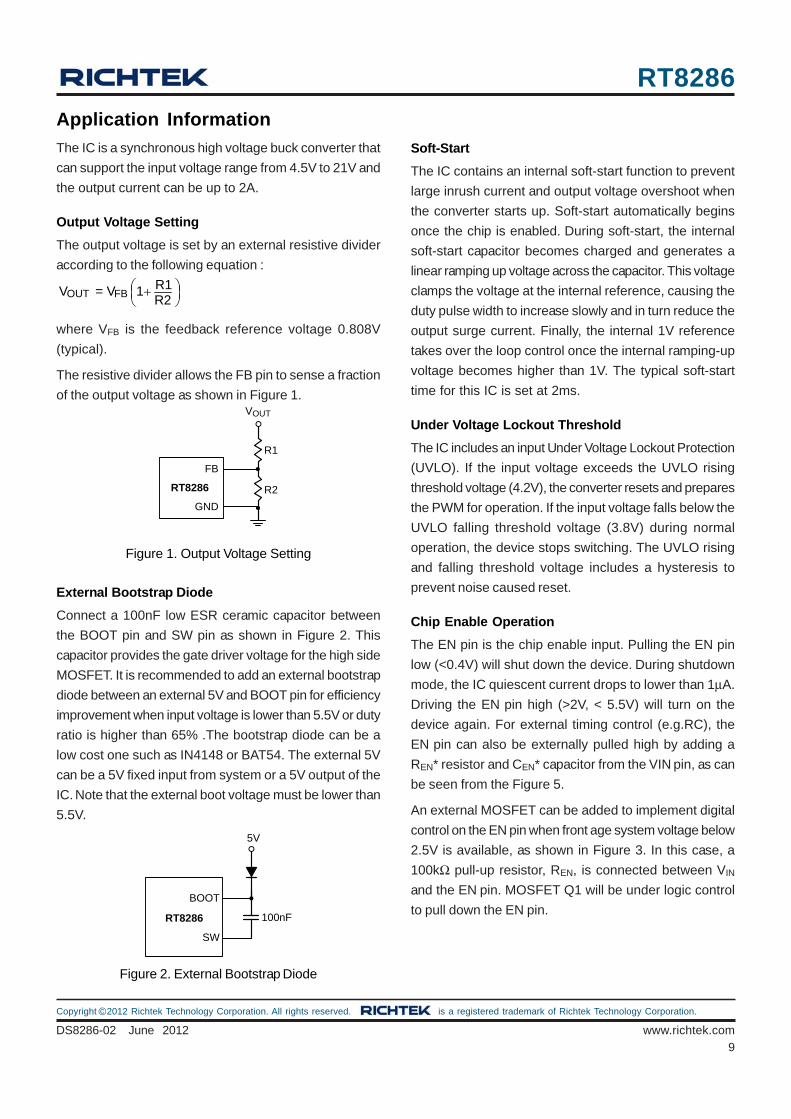
External Bootstrap DiodeConnect a 100nF low ESR ceramic capacitor betweenthe BOOT pin and SW pin as shown in Figure 2. Thiscapacitor provides the gate driver voltage for the high sideMOSFET. It is recommended to add an external bootstrapdiode between an external 5V and BOOT pin for efficiencyimprovement when input voltage is lower than 5.5V or dutyratio is higher than 65% .The bootstrap diode can be alow cost one such as IN4148 or BAT54. The external 5Vcan be a 5V fixed input from system or a 5V output of theIC. Note that the external boot voltage must be lower than5.5V.
Figure 2. External Bootstrap Diode
Soft-StartThe IC contains an internal soft-start function to preventlarge inrush current and output voltage overshoot whenthe converter starts up. Soft-start automatically beginsonce the chip is enabled. During soft-start, the internalsoft-start capacitor becomes charged and generates alinear ramping up voltage across the capacitor. This voltageclamps the voltage at the internal reference, causing theduty pulse width to increase slowly and in turn reduce theoutput surge current. Finally, the internal 1V referencetakes over the loop control once the internal ramping-upvoltage becomes higher than 1V. The typical soft-starttime for this IC is set at 2ms.
Under Voltage Lockout ThresholdThe IC includes an input Under Voltage Lockout Protection(UVLO). If the input voltage exceeds the UVLO risingthreshold voltage (4.2V), the converter resets and preparesthe PWM for operation. If the input voltage falls below theUVLO falling threshold voltage (3.8V) during normaloperation, the device stops switching. The UVLO risingand falling threshold voltage includes a hysteresis toprevent noise caused reset.
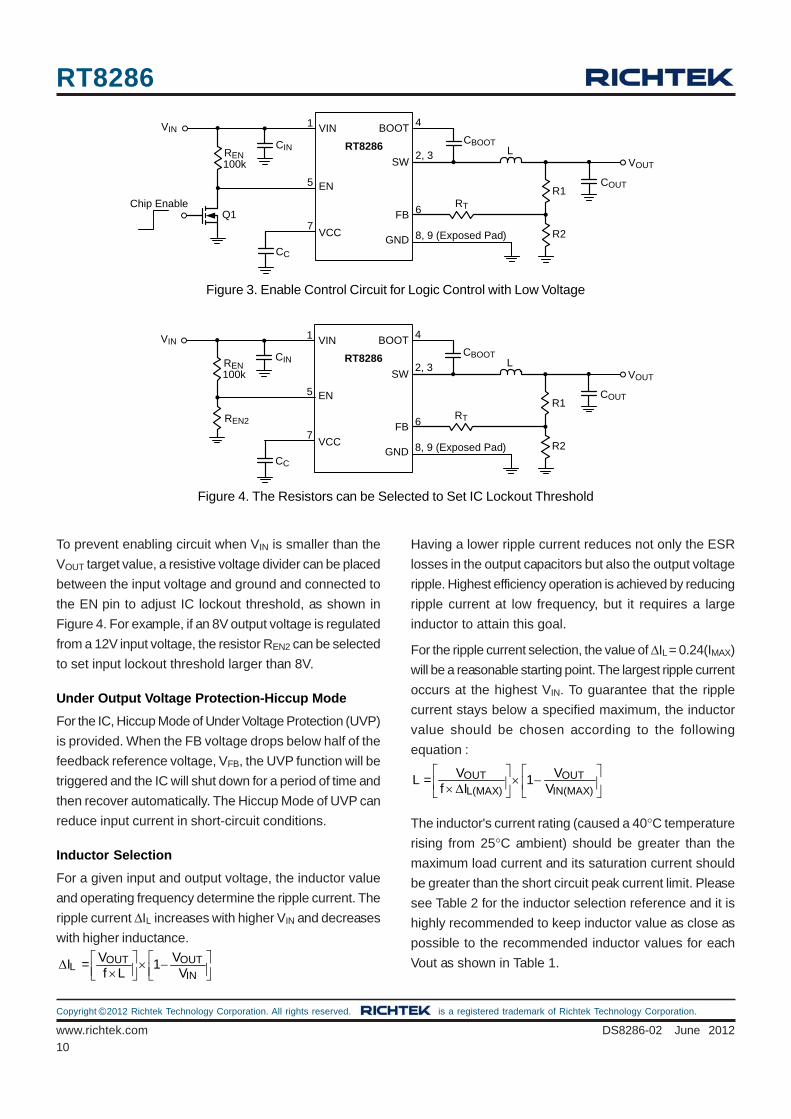
Chip Enable OperationThe EN pin is the chip enable input. Pulling the EN pinlow (<0.4V) will shut down the device. During shutdownmode, the IC quiescent current drops to lower than 1μA.Driving the EN pin high (>2V, < 5.5V) will turn on thedevice again. For external timing control (e.g.RC), theEN pin can also be externally pulled high by adding aREN* resistor and CEN* capacitor from the VIN pin, as canbe seen from the Figure 5.
An external MOSFET can be added to implement digitalcontrol on the EN pin when front age system voltage below2.5V is available, as shown in Figure 3. In this case, a100kΩ pull-up resistor, REN, is connected between VIN
and the EN pin. MOSFET Q1 will be under logic controlto pull down the EN pin.
⎛ ⎞+⎜ ⎟⎝ ⎠
OUT FBR1V = V 1R2
RT8286
GND
FB
R1
R2
VOUT
SW
BOOT
5V
100nFRT8286
RT8286
10DS8286-02 June 2012www.richtek.com
©Copyright 2012 Richtek Technology Corporation. All rights reserved. is a registered trademark of Richtek Technology Corporation.
Figure 3. Enable Control Circuit for Logic Control with Low Voltage
Figure 4. The Resistors can be Selected to Set IC Lockout Threshold
To prevent enabling circuit when VIN is smaller than theVOUT target value, a resistive voltage divider can be placedbetween the input voltage and ground and connected tothe EN pin to adjust IC lockout threshold, as shown inFigure 4. For example, if an 8V output voltage is regulatedfrom a 12V input voltage, the resistor REN2 can be selectedto set input lockout threshold larger than 8V.
Under Output Voltage Protection-Hiccup ModeFor the IC, Hiccup Mode of Under Voltage Protection (UVP)is provided. When the FB voltage drops below half of thefeedback reference voltage, VFB, the UVP function will betriggered and the IC will shut down for a period of time andthen recover automatically. The Hiccup Mode of UVP canreduce input current in short-circuit conditions.
Inductor SelectionFor a given input and output voltage, the inductor valueand operating frequency determine the ripple current. Theripple current ΔIL increases with higher VIN and decreaseswith higher inductance.
VIN
VCC
BOOT
FB
SW
6
1
2, 3
4
L
R1
R2
VOUT
VIN
RT8286
7
CBOOT
COUT
CIN
RT
EN
CC
5
Q1
REN100k
Chip Enable
GND 8, 9 (Exposed Pad)
REN2
VIN
VCC
BOOT
FB
SW
6
1
2, 3
4
L
R1
R2
VOUT
VIN
RT8286
7
CBOOT
COUT
CIN
RT
EN
CC
5
REN100k
GND 8, 9 (Exposed Pad)
Having a lower ripple current reduces not only the ESRlosses in the output capacitors but also the output voltageripple. Highest efficiency operation is achieved by reducingripple current at low frequency, but it requires a largeinductor to attain this goal.
For the ripple current selection, the value of ΔIL = 0.24(IMAX)will be a reasonable starting point. The largest ripple currentoccurs at the highest VIN. To guarantee that the ripplecurrent stays below a specified maximum, the inductorvalue should be chosen according to the followingequation :
The inductor's current rating (caused a 40°C temperaturerising from 25°C ambient) should be greater than themaximum load current and its saturation current shouldbe greater than the short circuit peak current limit. Pleasesee Table 2 for the inductor selection reference and it ishighly recommended to keep inductor value as close aspossible to the recommended inductor values for eachVout as shown in Table 1.OUT OUTL
INV VI = 1f L V
⎡ ⎤ ⎡ ⎤Δ × −⎢ ⎥ ⎢ ⎥×⎣ ⎦ ⎣ ⎦
OUT OUTL(MAX) IN(MAX)
V VL = 1f I V⎡ ⎤ ⎡ ⎤
× −⎢ ⎥ ⎢ ⎥× Δ⎣ ⎦ ⎣ ⎦
RT8286
11DS8286-02 June 2012 www.richtek.com
©Copyright 2012 Richtek Technology Corporation. All rights reserved. is a registered trademark of Richtek Technology Corporation.
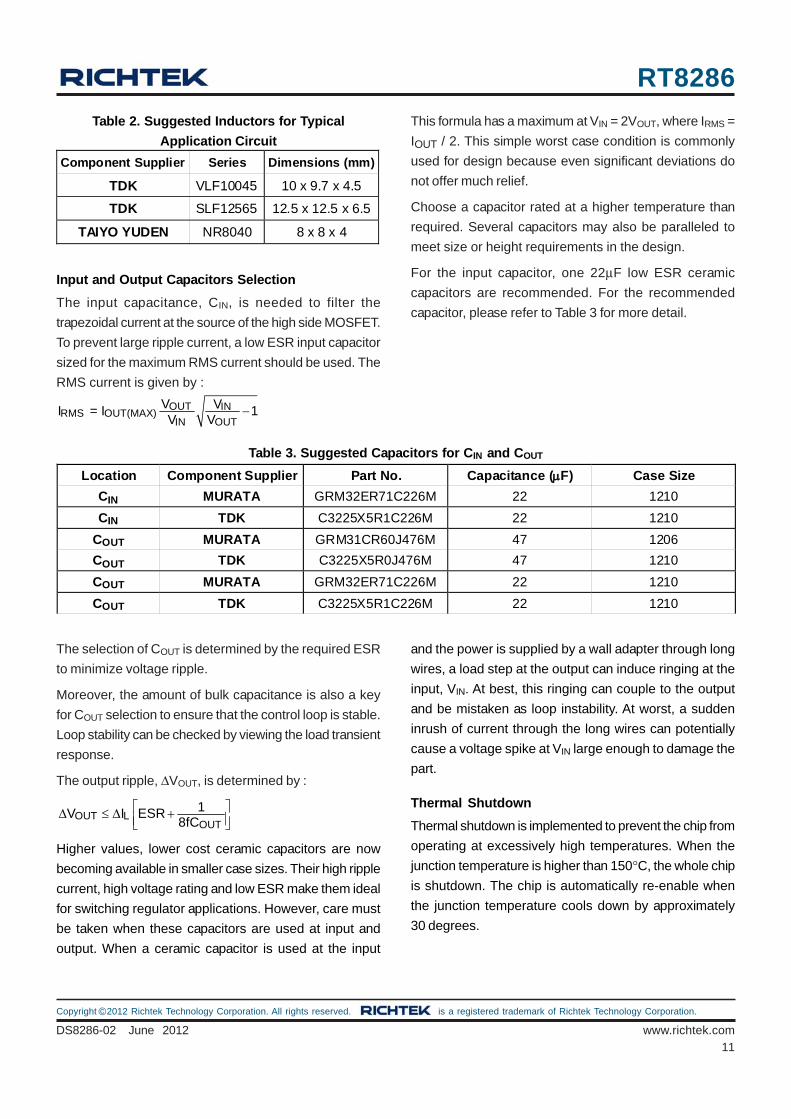
Table 2. Suggested Inductors for TypicalApplication Circuit
Component Supplier Series Dimensions (mm)
TDK VLF10045 10 x 9.7 x 4.5
TDK SLF12565 12.5 x 12.5 x 6.5
TAIYO YUDEN NR8040 8 x 8 x 4
Input and Output Capacitors SelectionThe input capacitance, CIN, is needed to filter thetrapezoidal current at the source of the high side MOSFET.To prevent large ripple current, a low ESR input capacitorsized for the maximum RMS current should be used. TheRMS current is given by :
This formula has a maximum at VIN = 2VOUT, where IRMS =IOUT / 2. This simple worst case condition is commonlyused for design because even significant deviations donot offer much relief.
Choose a capacitor rated at a higher temperature thanrequired. Several capacitors may also be paralleled tomeet size or height requirements in the design.
For the input capacitor, one 22μF low ESR ceramiccapacitors are recommended. For the recommendedcapacitor, please refer to Table 3 for more detail.
OUT INRMS OUT(MAX)IN OUT
V VI = I 1V V
−
Table 3. Suggested Capacitors for CIN and COUT
Location Component Supplier Part No. Capacitance (μF) Case Size CIN MURATA GRM32ER71C226M 22 1210 CIN TDK C3225X5R1C226M 22 1210
COUT MURATA GRM31CR60J476M 47 1206 COUT TDK C3225X5R0J476M 47 1210 COUT MURATA GRM32ER71C226M 22 1210 COUT TDK C3225X5R1C226M 22 1210
The selection of COUT is determined by the required ESRto minimize voltage ripple.
Moreover, the amount of bulk capacitance is also a keyfor COUT selection to ensure that the control loop is stable.Loop stability can be checked by viewing the load transientresponse.
The output ripple, ΔVOUT, is determined by :
Higher values, lower cost ceramic capacitors are nowbecoming available in smaller case sizes. Their high ripplecurrent, high voltage rating and low ESR make them idealfor switching regulator applications. However, care mustbe taken when these capacitors are used at input andoutput. When a ceramic capacitor is used at the input
OUT LOUT1V I ESR
8fC⎡ ⎤Δ ≤ Δ +⎢ ⎥⎣ ⎦
and the power is supplied by a wall adapter through longwires, a load step at the output can induce ringing at theinput, VIN. At best, this ringing can couple to the outputand be mistaken as loop instability. At worst, a suddeninrush of current through the long wires can potentiallycause a voltage spike at VIN large enough to damage thepart.
Thermal ShutdownThermal shutdown is implemented to prevent the chip fromoperating at excessively high temperatures. When thejunction temperature is higher than 150°C, the whole chipis shutdown. The chip is automatically re-enable whenthe junction temperature cools down by approximately30 degrees.

RT8286
12DS8286-02 June 2012www.richtek.com
©Copyright 2012 Richtek Technology Corporation. All rights reserved. is a registered trademark of Richtek Technology Corporation.
EMI ConsiderationSince parasitic inductance and capacitance effects in PCBcircuitry would cause a spike voltage on SW pin whenhigh side MOSFET is turned-on/off, this spike voltage onSW may impact on EMI performance in the system. Inorder to enhance EMI performance, there are two methodsto suppress the spike voltage. One way is by placing anR-C snubber (RS*, CS*) between SW and GND and locatingthem as close as possible to the SW pin, as shown in
Figure 5. Reference Circuit with Snubber and Enable Timing Control
REN*
CEN*
* : Optional
VIN
VCC
BOOT
FB
SW
6
1
2, 3
4
L
R1
R2
VOUT
VIN
RT8286
7
CBOOT
COUT
CIN
RT
EN
CC
5
GND 8, 9 (Exposed Pad)
CS*
RS*
Figure 5. Another method is by adding a resistor in serieswith the bootstrap capacitor, CBOOT, but this method willdecrease the driving capability to the high side MOSFET.It is strongly recommended to reserve the R-C snubberduring PCB layout for EMI improvement. Moreover,reducing the SW trace area and keeping the main powerin a small loop will be helpful on EMI performance. Fordetailed PCB layout guide, please refer to the sectionLayout Considerations.
Thermal ConsiderationsFor continuous operation, do not exceed absolutemaximum junction temperature. The maximum powerdissipation depends on the thermal resistance of the ICpackage, PCB layout, rate of surrounding airflow, anddifference between junction and ambient temperature. Themaximum power dissipation can be calculated by thefollowing formula :
PD(MAX) = (TJ(MAX) − TA) / θJA
where TJ(MAX) is the maximum junction temperature, TA isthe ambient temperature, and θJA is the junction to ambientthermal resistance.
For recommended operating condition specifications, themaximum junction temperature is 125°C. The junction toambient thermal resistance, θJA, is layout dependent. ForSOP-8 (Exposed Pad) packages, the thermal resistance,θJA, is 75°C/W on a standard JEDEC 51-7 four-layerthermal test board. The maximum power dissipation atTA = 25°C can be calculated by the following formula :
PD(MAX) = (125°C − 25°C) / (75°C/W) = 1.333W forSOP-8 (Exposed Pad) package
Figure 6. Derating Curve of Maximum Power Dissipation
0.0
0.2
0.4
0.6
0.8
1.0
1.2
1.4
0 25 50 75 100 125
Ambient Temperature (°C)
Max
imum
Pow
er D
issi
patio
n (W
) Four-Layer PCB
The maximum power dissipation depends on the operatingambient temperature for fixed TJ(MAX) and thermalresistance, θJA. The derating curve in Figure 6 allows thedesigner to see the effect of rising ambient temperatureon the maximum power dissipation.

RT8286
13DS8286-02 June 2012 www.richtek.com
©Copyright 2012 Richtek Technology Corporation. All rights reserved. is a registered trademark of Richtek Technology Corporation.
Figure 7. PCB Layout Guide
Layout ConsiderationsFollow the PCB layout guidelines for optimal performanceof the IC.
Keep the traces of the main current paths as short andwide as possible.
Put the input capacitor as close as possible to the devicepins (VIN and GND).
SW node is with high frequency voltage swing andshould be kept at small area. Keep analog componentsaway from the SW node to prevent stray capacitive noisepickup.
CIN
CBOOT
VOUTCOUT
GND
VOUT
RTR2
R1
L
GND
Place the input and output capacitors as close to the IC as possible.
SW should be connected to inductor by wide and short trace and keep sensitive components away from this trace.
Place the feedback as close to the IC as possible.
VINSWSW
BOOT
GNDVCC
ENFB
GND2
3
4 5
6
7
8
9
Connect feedback network behind the output capacitors.Keep the loop area small. Place the feedbackcomponents near the IC.
Connect all analog grounds to a common node and thenconnect the common node to the power ground behindthe output capacitors.
An example of PCB layout guide is shown in Figure 7.for reference.

RT8286
14DS8286-02 June 2012www.richtek.com
Richtek Technology Corporation5F, No. 20, Taiyuen Street, Chupei CityHsinchu, Taiwan, R.O.C.Tel: (8863)5526789
Richtek products are sold by description only. Richtek reserves the right to change the circuitry and/or specifications without notice at any time. Customers shouldobtain the latest relevant information and data sheets before placing orders and should verify that such information is current and complete. Richtek cannotassume responsibility for use of any circuitry other than circuitry entirely embodied in a Richtek product. Information furnished by Richtek is believed to beaccurate and reliable. However, no responsibility is assumed by Richtek or its subsidiaries for its use; nor for any infringements of patents or other rights of thirdparties which may result from its use. No license is granted by implication or otherwise under any patent or patent rights of Richtek or its subsidiaries.
Outline Dimension
A
BJ
F
H
M
C
D
I
Y
X
EXPOSED THERMAL PAD(Bottom of Package)
8-Lead SOP (Exposed Pad) Plastic Package
Dimensions In Millimeters Dimensions In Inches Symbol
Min Max Min Max
A 4.801 5.004 0.189 0.197
B 3.810 4.000 0.150 0.157
C 1.346 1.753 0.053 0.069
D 0.330 0.510 0.013 0.020
F 1.194 1.346 0.047 0.053
H 0.170 0.254 0.007 0.010
I 0.000 0.152 0.000 0.006
J 5.791 6.200 0.228 0.244
M 0.406 1.270 0.016 0.050
X 2.000 2.300 0.079 0.091 Option 1
Y 2.000 2.300 0.079 0.091
X 2.100 2.500 0.083 0.098 Option 2
Y 3.000 3.500 0.118 0.138
Related Documents