Row-Based Area-Array I/O Design Planning in Concurrent Chip- Package Design Flow R. Lee and H. Chen Department of EE NCTU, Taiwan ASPDAC 2011

Row-Based Area-Array I/O Design Planning in Concurrent Chip-Package Design Flow R. Lee and H. Chen Department of EE NCTU, Taiwan ASPDAC 2011.
Dec 17, 2015
Welcome message from author
This document is posted to help you gain knowledge. Please leave a comment to let me know what you think about it! Share it to your friends and learn new things together.
Transcript
Row-Based Area-Array I/O Design Planning in Concurrent Chip-Package Design Flow
R. Lee and H. Chen
Department of EE
NCTU, Taiwan
ASPDAC 2011

Outline
Introduction Novel I/O-bump tile design and I/O-row based
planning Package-aware I/O-bump planning methods Experimental results Conclusion
Introduction
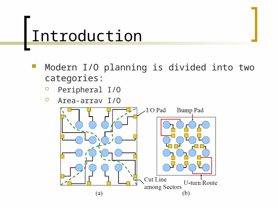
Modern I/O planning is divided into two categories: Peripheral I/O Area-array I/O
Introduction
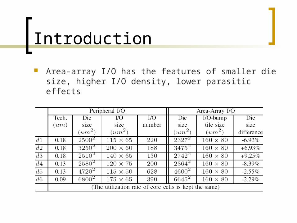
Area-array I/O has the features of smaller die size, higher I/O density, lower parasitic effects

Introduction
Flip-chip
RDL routing
Introduction
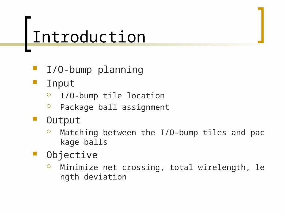
I/O-bump planning Input
I/O-bump tile location Package ball assignment
Output Matching between the I/O-bump tiles and package balls
Objective Minimize net crossing, total wirelength, length deviation
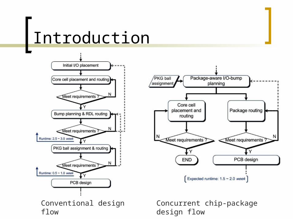
Introduction
Conventional design flow Concurrent chip-package design flow
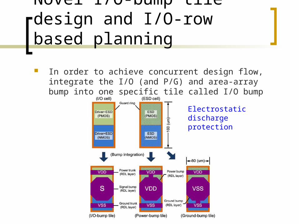
Novel I/O-bump tile design and I/O-row based planning
In order to achieve concurrent design flow, integrate the I/O (and P/G) and area-array bump into one specific tile called I/O bump
Electrostatic discharge protection
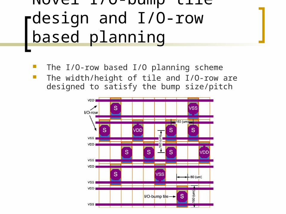
Novel I/O-bump tile design and I/O-row based planning
The I/O-row based I/O planning scheme The width/height of tile and I/O-row are designed to satisfy the
bump size/pitch
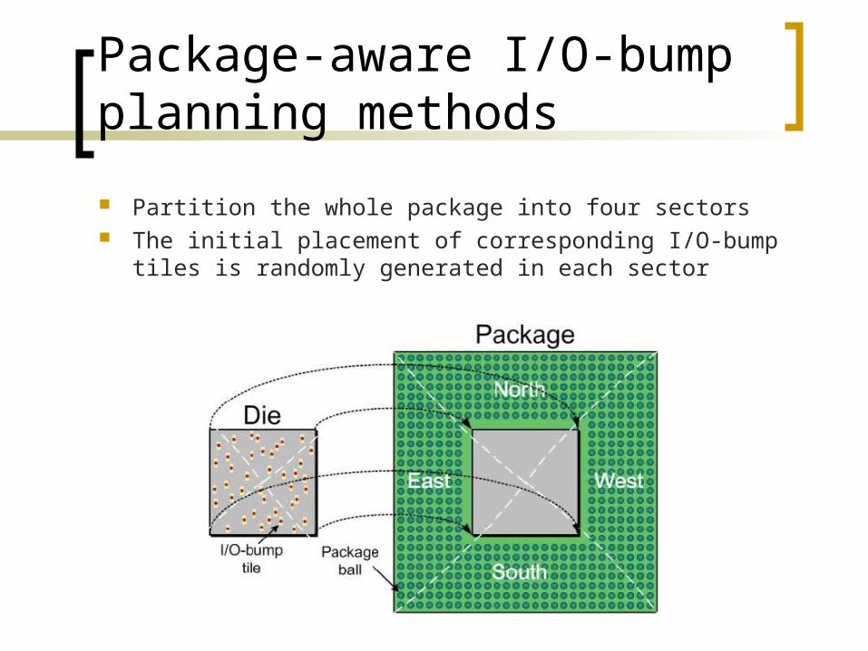
Package-aware I/O-bump planning methods
Partition the whole package into four sectors The initial placement of corresponding I/O-bump
tiles is randomly generated in each sector

Package-aware I/O-bump planning methods
Double sorting for planar planning (SORT) Sort package balls (top to bottom, outer to inner) Sort I/O-bump tiles (top to bottom, inner to outer) Balls and bumps which have the same numbers will be
paired for connection
1
2
1
2

Package-aware I/O-bump planning methods
SORT method intuitively succeeds in producing a zero-crossing package routing
However, the net length is another critical factor, nets from bumps to balls should be routed as short as possible
Each net should be kept in the similar wirelength
Apply a greedy way to shorten the total wirelength and the length deviation called GREEDY
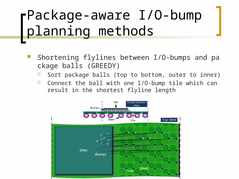
Package-aware I/O-bump planning methods
Shortening flylines between I/O-bumps and package balls (GREEDY) Sort package balls (top to bottom, outer to inner) Connect the ball with one I/O-bump tile which can result in
the shortest flyline length
Package-aware I/O-bump planning methods
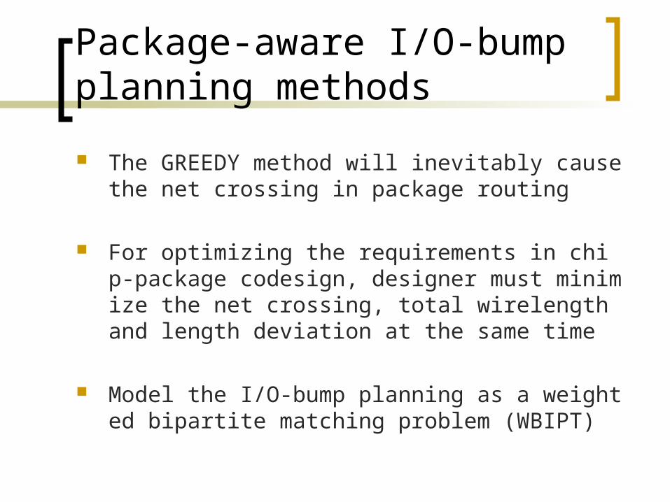
The GREEDY method will inevitably cause the net crossing in package routing
For optimizing the requirements in chip-package codesign, designer must minimize the net crossing, total wirelength and length deviation at the same time
Model the I/O-bump planning as a weighted bipartite matching problem (WBIPT)

Package-aware I/O-bump planning methods
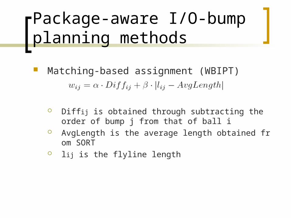
Matching-based assignment (WBIPT)
xij = 1 if ball i is assigned to bump j m and n are the total number of balls and bumps
Package-aware I/O-bump planning methods
Matching-based assignment (WBIPT)
Diffij is obtained through subtracting the order of bump j from that of ball i
AvgLength is the average length obtained from SORT lij is the flyline length
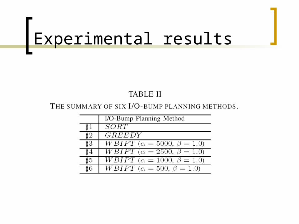
Experimental results

Experimental results

Experimental results

Experimental results
Conclusion
With the setup in the design of I/O-bump tile and I/O-row based scheme, this paper develop a chip-package concurrent design flow
Related Documents