Rotary Micro-Ball Bearing Designs for MEMS Applications Robert J. Hergert A thesis submitted to Imperial College London in fulfilment of the requirements for the Degree of Doctor of Philosophy (PhD) and the Diploma of Imperial College Optical and Semiconductor Devices Group Department of Electrical and Electronic Engineering Imperial College London August 2013

Welcome message from author
This document is posted to help you gain knowledge. Please leave a comment to let me know what you think about it! Share it to your friends and learn new things together.
Transcript

Rotary Micro-Ball Bearing Designs for MEMSApplications
Robert J. Hergert
A thesis submitted to Imperial College London in fulfilmentof the requirements for
the Degree of Doctor of Philosophy (PhD)and the Diploma of Imperial College
Optical and Semiconductor Devices GroupDepartment of Electrical and Electronic Engineering
Imperial College London
August 2013

Declaration of Copyright
The author declares that the work presented in this thesis is his own. The
works by others have been appropriately cited and acknowledged.
The copyright of this thesis rests with the author and is made available
under a Creative Commons Attribution Non-Commercial No Derivatives li-
cence. Researchers are free to copy, distribute or transmit the thesis on the
condition that they attribute it, that they do not use it for commercial pur-
poses and that they do not alter, transform or build upon it. For any reuse
or redistribution, researchers must make clear to others the licence terms of
this work.
2

Acknowledgements
I would first of all like to thank my very understanding and supportive wife
Sarah Nolton Hergert. For her love, patience and support throughout this
research. Without her none of this would have been possible.
I greatly appreciate Prof. Andrew Holmes for agreeing to take on this project
and me as a student. Your insight, support, and help have been greatly val-
ued. It was extremely educational and enjoyable working with you. Your
vast knowledge and keen mind were invaluable assets.
I would also like to express my appreciation to to the following colleagues:
• Dr. Munir Ahmad for all of your help with fabrication processes and
equipment. Without your training and support none of these devices
would have been possible.
• Dr. Werner Karl for your friendship, brilliant ideas, teaching and pa-
tience in the cleanroom. You helped me with many problems and en-
couraged me to try new things.
• Dr. Ingrid Ku and Dr. Tom Reddyhoff for your help with tribometer
testing and expanding my knowledge of tribology. The time you spent
helping me was much appreciated.
• Phil Jones for letting me use the machine shop and for teaching me
how to better design and built test equipment.
• Dr. Robert Maher and Dr. Kai Herbertz for your friendship and for
3

helping to keep me somewhat sane. Thanks for all of the distractions
and good times.
• Susan Brace for everything that you do for the group and for making
all of our lives easier.
• Dr. Edd Davies, Dr. Aifric Delahunty, Dr. Kaushal Choonee, Dr.
Tzern Toh, Pit Pillatsch, Dr. Anisha Mukherjee, Anshu Bansal, Will
Otter, Emilijana Krali, Dr. Timmy Floume and anyone who I may
have forgotten for your help, friendship and for making the group a
great place to work.
• Prof. Tom Pike and Dr. Mike Ward for taking the time and effort to
review this thesis.
4

Abstract
Micro-electro-mechanical systems (MEMS) technology allows the fabrication
of small mechanical systems in silicon using standard micro-fabrication pro-
cesses. MEMS techniques have found wide acceptance in such devices as ac-
celerometers, micro-mirrors, resonators, probes, and micro-tweezers to name
a few. Though small linear motions are common in MEMS applications, few
devices exhibit reliable rotary motion. This work explores several methods
of fabricating rotary bearings using micro-balls as the support mechanism.
Micro-ball bearings have several advantages over other MEMS bearing tech-
nologies in that they provide robust mechanical support, require no external
control systems, and basic designs require very few fabrication steps.
Ball cages or retainers are common in macro-scale bearings, providing
uniform spacing between the balls. Several cage designs are proposed and
explored in this work: a radial ball bearing with an integrated ball cage, a
dual-row style cage, and five unique cage geometries integrated into silicon
micro-turbines (SMTs.) Also, an example of a curved or angular contact race-
way is presented as an example of this type of raceway geometry in MEMS
devices. Each is presented with a discussion of the design considerations and
fabrication process. This is followed by a characterization of the performance
of each design.
These studies found that the integrated cage in the radial ball bearing
performs well at speeds ranging up to 20 000 RPM. Minimal wear was ob-
served after 6 hours of continuous testing. However, the solder bond in the
cage was a common failure point in these devices, limiting the reliability and
longevity. The dual groove style cage was designed to eliminate the solder
bond. However, the higher frictional forces between the ball and the cage in
5

this design resulted in higher losses during operation. Taking into account the
higher losses and the added complexity of the design, it seems unlikely that
this approach would be appropriate for further study. However, the design
does represent a novel approach for releasing multi-wafer rotary structures
and is presented here as example of this technique. Testing of the cage de-
signs for the SMTs indicated that a full ring design (a full annulus with holes
for the balls) performed the best of the 5 cage geometries. However, these
devices do not perform as well as cage-less designs for high speed applications
due to higher fictional forces and increased raceway wear at the interface be-
tween the ball and the raceway edge. Finally, the curved raceway has shown
excellent performance up to 2500 RPM with normal loads up to 40 mN in
tribometer testing. SMTs with this raceway desing were also tested for over
10 million revolutions and at speeds over 70 000 RPM. The test results for all
of the bearings designs presented here show that the devices exhibit stable
operation at low to moderately high speeds.
6

Contents
Acknowledgments 3
Abstract 5
Table of Contents 7
List of Figures 8
List of Tables 9
Nomenclature 10
1 Introduction 141.1 Background . . . . . . . . . . . . . . . . . . . . . . . . . . . . 141.2 Motivation and Goals . . . . . . . . . . . . . . . . . . . . . . . 161.3 Research Objectives . . . . . . . . . . . . . . . . . . . . . . . . 161.4 Description of Thesis . . . . . . . . . . . . . . . . . . . . . . . 17
2 Bearings in MEMS Devices 192.1 Competing Bearing Technologies . . . . . . . . . . . . . . . . 192.2 Pin Joint Bearing . . . . . . . . . . . . . . . . . . . . . . . . . 202.3 Magnetic or Electrostatic Levitation . . . . . . . . . . . . . . 222.4 Jewel Bearing . . . . . . . . . . . . . . . . . . . . . . . . . . . 222.5 Air Bearing . . . . . . . . . . . . . . . . . . . . . . . . . . . . 232.6 Liquid Bearing . . . . . . . . . . . . . . . . . . . . . . . . . . 262.7 Previous Work in Micro-Ball Bearings . . . . . . . . . . . . . . 27
2.7.1 Linear Micro-Ball Bearing . . . . . . . . . . . . . . . . 272.7.2 Rotary Micro-Ball Bearings . . . . . . . . . . . . . . . 292.7.3 Conventional Micro-Ball Bearings . . . . . . . . . . . . 30
2.8 Discussion and Conclusions . . . . . . . . . . . . . . . . . . . 32
7

3 Micro-Fabrication Technologies 333.1 Patterning and Masking . . . . . . . . . . . . . . . . . . . . . 33
3.1.1 Photo-Masks . . . . . . . . . . . . . . . . . . . . . . . 343.1.2 Photolithography . . . . . . . . . . . . . . . . . . . . . 343.1.3 Masking Materials . . . . . . . . . . . . . . . . . . . . 35
3.1.3.1 Photoresist . . . . . . . . . . . . . . . . . . . 353.1.3.2 Silicon Dioxide . . . . . . . . . . . . . . . . . 36
3.2 Deep Reaction Ion Etching (DRIE) . . . . . . . . . . . . . . . 373.2.1 Basic Principles . . . . . . . . . . . . . . . . . . . . . . 373.2.2 Through-Wafer Etching . . . . . . . . . . . . . . . . . 383.2.3 Halo Mask for Through Wafer Etching . . . . . . . . . 393.2.4 Etch Lag . . . . . . . . . . . . . . . . . . . . . . . . . . 40
3.3 Electroplating . . . . . . . . . . . . . . . . . . . . . . . . . . . 413.4 Eutectic and Solder Wafer Bonding . . . . . . . . . . . . . . . 433.5 Conclusion . . . . . . . . . . . . . . . . . . . . . . . . . . . . . 44
4 Ball Bearing Design Considerations 454.1 Ball Cage . . . . . . . . . . . . . . . . . . . . . . . . . . . . . 464.2 Raceway and Roller Element Materials . . . . . . . . . . . . . 494.3 Raceway Geometry . . . . . . . . . . . . . . . . . . . . . . . . 504.4 Raceway Tolerance . . . . . . . . . . . . . . . . . . . . . . . . 544.5 Raceway Fill . . . . . . . . . . . . . . . . . . . . . . . . . . . . 554.6 Wear . . . . . . . . . . . . . . . . . . . . . . . . . . . . . . . . 564.7 Bearing Loss . . . . . . . . . . . . . . . . . . . . . . . . . . . . 574.8 Discussion and Conclusions . . . . . . . . . . . . . . . . . . . 61
5 Testing Methodologies 635.1 Tribometer . . . . . . . . . . . . . . . . . . . . . . . . . . . . 63
5.1.1 Tribometer Measurement Technique . . . . . . . . . . . 645.1.2 Test Platform . . . . . . . . . . . . . . . . . . . . . . . 66
5.1.2.1 Torque Measurement Platform (Inner Plat-form) . . . . . . . . . . . . . . . . . . . . . . 66
5.1.2.2 Normal Load Measurement Platform (OuterPlatform) . . . . . . . . . . . . . . . . . . . . 69
5.1.3 Tribometer Setup and Operation . . . . . . . . . . . . 715.2 Silicon Micro-Turbine (SMT) . . . . . . . . . . . . . . . . . . 76
5.2.1 Turbine Design and Operation . . . . . . . . . . . . . . 775.2.2 Testing Setup . . . . . . . . . . . . . . . . . . . . . . . 79
5.3 Discussion and Conclusions . . . . . . . . . . . . . . . . . . . 86
8

6 Proof of Concept of a Radial Ball Bearing with IntegratedBall Cage 886.1 Design . . . . . . . . . . . . . . . . . . . . . . . . . . . . . . . 896.2 Device Fabrication . . . . . . . . . . . . . . . . . . . . . . . . 91
6.2.1 Step A - Plate Solder Pads . . . . . . . . . . . . . . . . 916.2.2 Step B - Etch Cage Arms and Bearing Raceway . . . . 926.2.3 Step C - Pattern Cage Release Channels . . . . . . . . 926.2.4 Step D - Device Assembly . . . . . . . . . . . . . . . . 926.2.5 Step E - Release Etch . . . . . . . . . . . . . . . . . . 926.2.6 Fabricated Devices . . . . . . . . . . . . . . . . . . . . 93
6.3 Testing . . . . . . . . . . . . . . . . . . . . . . . . . . . . . . . 946.3.1 Cage Bond Failure . . . . . . . . . . . . . . . . . . . . 956.3.2 Tribometer Results . . . . . . . . . . . . . . . . . . . . 966.3.3 Wear . . . . . . . . . . . . . . . . . . . . . . . . . . . . 99
6.4 Discussion and Conclusions . . . . . . . . . . . . . . . . . . . 101
7 In-Situ Fabrication of a Monolithic Silicon Ball Cage 1037.1 Design . . . . . . . . . . . . . . . . . . . . . . . . . . . . . . . 1057.2 Device Fabrication . . . . . . . . . . . . . . . . . . . . . . . . 110
7.2.1 Top and Bottom Die Fabrication . . . . . . . . . . . . 1107.2.1.1 Step A (Front Side)- Plate Solder Pads . . . . 1117.2.1.2 Step B (Front Side) - Pattern Raceway Stand-
off Trench . . . . . . . . . . . . . . . . . . . . 1127.2.1.3 Step C (Front Side) - Pattern the Raceway
and Etch the Raceway Stand-Off . . . . . . . 1127.2.1.4 Step D (Front Side) - Etch Bearing Raceway . 1127.2.1.5 Step E (Back Side) - Define Cage Release
Window and Identification Marks . . . . . . . 1127.2.1.6 Step F (Back Side) - Define Testing Adaptor
Feature and Bearing Release Channels; Pre-Etch Cage Release Window . . . . . . . . . . 113
7.2.1.7 Step G (Back Side) - Pre-Etch Testing Adap-tor Feature and Bearing Release Channels;Etch Cage Release Window Through the Wafer113
7.2.1.8 Images of Fabricated Top and Bottom Die . . 1137.2.2 Center Die Fabrication . . . . . . . . . . . . . . . . . . 115
7.2.2.1 Step A (Top Side) - Plate Solder Pads . . . . 1167.2.2.2 Step B (Top Side) - Define Cage with Support
Beams . . . . . . . . . . . . . . . . . . . . . . 1177.2.2.3 Step C (Back Side) - Plate Solder Pads . . . . 117
9

7.2.2.4 Step D (Back Side) - Define Cage with Sup-port Beams . . . . . . . . . . . . . . . . . . . 117
7.2.2.5 Step E (Back Side) - Pattern Cage With-out Support Beams and Pre-Etch Cage WithSupport Beams . . . . . . . . . . . . . . . . . 117
7.2.2.6 Step F (Back Side) - Etch Cage to Final Depthand Reduce Beam Thickness . . . . . . . . . 118
7.2.2.7 Step G (Top Side) - Pattern Cage WithoutSupport Beams and Pre-Etch Cage With Sup-port Beams . . . . . . . . . . . . . . . . . . . 118
7.2.2.8 Step H (Top Side) Etch Area Around CageThrough the Wafer and Reduce the BeamThickness . . . . . . . . . . . . . . . . . . . . 118
7.2.2.9 Images of Fabricated Center Die . . . . . . . 1197.2.3 Device Assembly and Release Etching . . . . . . . . . . 120
7.2.3.1 Step A - Device Assembly . . . . . . . . . . . 1217.2.3.2 Step B - Release Etching . . . . . . . . . . . . 1227.2.3.3 Images of Assembled and Released Devices . . 123
7.3 Testing . . . . . . . . . . . . . . . . . . . . . . . . . . . . . . . 1247.4 Test Results . . . . . . . . . . . . . . . . . . . . . . . . . . . . 1247.5 Wear . . . . . . . . . . . . . . . . . . . . . . . . . . . . . . . . 1267.6 Discussion and Conclusions . . . . . . . . . . . . . . . . . . . 128
8 Micro-Turbines with Integrated Silicon Ball Cage 1308.1 Retainer Ring Design Considerations . . . . . . . . . . . . . . 1318.2 Retainer Ring Design Variations . . . . . . . . . . . . . . . . . 1368.3 SMT Design . . . . . . . . . . . . . . . . . . . . . . . . . . . . 1388.4 Device Fabrication . . . . . . . . . . . . . . . . . . . . . . . . 138
8.4.1 Retainer Fabrication . . . . . . . . . . . . . . . . . . . 1398.4.2 Turbine Wafer Fabrication . . . . . . . . . . . . . . . . 139
8.4.2.1 Step A (Top Side) - Electroplate Solder Pads 1418.4.2.2 Step B (Top Side) - Pattern Turbine Release
Channel . . . . . . . . . . . . . . . . . . . . . 1418.4.2.3 Step C (Top Side) - Pattern Cage Raceway
Standoff . . . . . . . . . . . . . . . . . . . . . 1418.4.2.4 Step D (Top Side) - Pattern Cage Raceway
and Etch Bearing Release Channel . . . . . . 1418.4.2.5 Step E (Top Side) - Etch Cage Raceway Stand
Off . . . . . . . . . . . . . . . . . . . . . . . . 1428.4.2.6 Step F (Top Side) - Etch Cage Raceway . . . 142
10

8.4.2.7 Step G (Back Side) - Pattern Turbine ReleaseChannel . . . . . . . . . . . . . . . . . . . . . 143
8.4.2.8 Step H (Back Side) - Pattern Turbine Bladeand Etch Bearing Release Channel . . . . . . 143
8.4.2.9 Step I (Back Side) - Pre-Etch Turbine Blades 1438.4.3 Thrust Wafer Fabrication . . . . . . . . . . . . . . . . 143
8.4.3.1 Step A (Top Side) - Electroplate Solder Pads 1448.4.3.2 Step B (Top Side) - Etch Bearing Raceway . 1448.4.3.3 Step C (Back Side) - Pattern and Pre-Etch
Thrust Release Channel . . . . . . . . . . . . 1458.4.4 Assembly and Release Etch . . . . . . . . . . . . . . . 145
8.4.4.1 Step A - Place Cage, Solder Balls, and SteelBalls in Thrust Die . . . . . . . . . . . . . . . 146
8.4.4.2 Step B - Align Turbine Die and Bond the Device1468.4.4.3 Step C - Turbine Release Etch . . . . . . . . 1478.4.4.4 Images of Fabricated SMT Devices with In-
tegrated Cages . . . . . . . . . . . . . . . . . 1478.5 Testing . . . . . . . . . . . . . . . . . . . . . . . . . . . . . . . 148
8.5.1 Comparison of Cage Design Performance . . . . . . . . 1498.5.2 Performance Repeatability . . . . . . . . . . . . . . . . 152
8.6 Longevity and Wear . . . . . . . . . . . . . . . . . . . . . . . 1538.7 Discussion and Conclusions . . . . . . . . . . . . . . . . . . . 155
9 Curved Raceway 1579.1 Device Design . . . . . . . . . . . . . . . . . . . . . . . . . . . 1579.2 Device Fabrication . . . . . . . . . . . . . . . . . . . . . . . . 159
9.2.1 Fabrication of SMTs with Angular Contact Raceways . 1599.2.1.1 Bearing Raceways . . . . . . . . . . . . . . . 1599.2.1.2 Turbine Side . . . . . . . . . . . . . . . . . . 1619.2.1.3 Thrust Side . . . . . . . . . . . . . . . . . . . 1629.2.1.4 Device Assembly . . . . . . . . . . . . . . . . 163
9.2.2 Fabrication of Devices for Tribometer Testing . . . . . 1649.2.2.1 Bearing Raceway . . . . . . . . . . . . . . . . 1649.2.2.2 Backside . . . . . . . . . . . . . . . . . . . . . 1669.2.2.3 Adaptor Side . . . . . . . . . . . . . . . . . . 1679.2.2.4 Device Assembly . . . . . . . . . . . . . . . . 168
9.2.3 Images of Fabricated Devices . . . . . . . . . . . . . . 1699.3 Performance . . . . . . . . . . . . . . . . . . . . . . . . . . . . 171
9.3.1 Performance of SMT with Angular Contact Raceway . 1719.3.2 Tribometer Measurements . . . . . . . . . . . . . . . . 1739.3.3 Wear . . . . . . . . . . . . . . . . . . . . . . . . . . . . 175
11

9.4 Discussion and Conclusions . . . . . . . . . . . . . . . . . . . 176
10 Conclusions and Further Work 17810.1 Contributions of this Thesis . . . . . . . . . . . . . . . . . . . 17810.2 Objectives Revisited . . . . . . . . . . . . . . . . . . . . . . . 17910.3 Conclusions . . . . . . . . . . . . . . . . . . . . . . . . . . . . 18210.4 Further Work . . . . . . . . . . . . . . . . . . . . . . . . . . . 182
11 List of Published Works 185
List of Published Works 185
Bibliography 201
A AZ9260 Photoresist Coating Process 202
12

List of Figures
2.1 A. Image of the gear arrangement in the polysilicon pin jointstudies; B. Excessive wear found on drive gear pin hole; C.Undamaged pin hole on side gear to compare with above im-age; D. Cross section of the pin joint bearing interface showingunworn structure (top) and worn structures (bottom). Imagesreproduced from [Tanner 98] . . . . . . . . . . . . . . . . . . . 21
2.2 Conceptual drawing of a common jewel bearing design, withjewels forming a cup on the stator to hold a pin attached tothe rotor. . . . . . . . . . . . . . . . . . . . . . . . . . . . . . 23
2.3 Optical photograph (top) and schematic (bottom) of the crosssection of a silicon micro-turbine supported on an air bearing.Diagram reproduced from [Frechette 05]. . . . . . . . . . . . . 24
2.4 Air bearing operating modes presented in [Hara 03]. Figurereproduced from [Hara 03]. . . . . . . . . . . . . . . . . . . . . 26
2.5 (a) Schematic of the linear micro-motor on micro-ball bearings(b) Square wave motor drive signal. Figure reproduced from[Modafe 06]. . . . . . . . . . . . . . . . . . . . . . . . . . . . . 28
2.6 A. Optical image of ball jamming in the bearing raceway; B.SEM image of ball without wear (top) and ball after 39 min.operation (bottom); C. SEM image of the unworn bonded sili-con raceway interface (top) and the worn bonded silicon race-way interface. Images reproduced from [Waits 07a]. . . . . . . 30
2.7 Picture of the Timken S100 micro-ball bearing, photo by TimkenCo. . . . . . . . . . . . . . . . . . . . . . . . . . . . . . . . . . 31
3.1 Halo mask concept (left) with the etch trenches in white, thedevice structure in pink and the sacrificial substrate in green.SEM (right) of a device fabricated by through wafer etchingusing a halo mask. . . . . . . . . . . . . . . . . . . . . . . . . 40
13

3.2 SEM image of high aspect ratio silicon trenches, with featuresizes ranging from 2.2 µm on the left to 5.5 µm on the right.Larger trench sizes have a higher etch rate and lower aspectratio. Image from [Chung 04]. . . . . . . . . . . . . . . . . . . 41
4.1 Examples of macro-scale cage designs. A. Nylon snap cage forball bearing, B. Nylon cage for cylindrical bearing, C. Nyloncage of high-angular-contact bearing, D. Phenolic cage for pre-cision ball bearing, E. Angular contact bearing with annularcage, F. deep-groove Conrad-assembly bearing with rivetedcage, G. Dual row ball bearing with snap cage, H. Thrustball bearing with annular cage design. Images reproducedfrom [Harris 06b]. . . . . . . . . . . . . . . . . . . . . . . . . . 48
4.2 Examples of the 2 raceway geometries explored in this thesis.The contact region for each race is indicated by the red regionsin the diagram, the rectangular raceway (left) provides smallerelliptical contacts, while the curved (angular) raceway (right)provides much larger elongated elliptical contact regions. Athrust load (W) is applied to the rotor as indicated by theblue arrow. . . . . . . . . . . . . . . . . . . . . . . . . . . . . 51
4.3 The contact angle (α) is shown for a ball bearing under thrustload. The contact angle is the angle at which the ball contactsthe raceway under load or during operation. The contact anglecan be different between at the rotor and the stator. . . . . . . 51
4.4 Parameters for Calculating Pd. . . . . . . . . . . . . . . . . . . 554.5 Examples of wear and denting on macro-scale bearings. A.
Smearing on the raceway of a tapered bearing, B. Extrememicropitting on ball bearing inner raceway, C. Advanced sur-face initiated fatigue on a thrust ball bearing, and D. Rollingelement denting of a ball. Images from [Harris 06a]. . . . . . . 57
4.6 Diagram showing the net force on the stator from clockwisemotion of the rotor during sliding (clockwise) and rolling (an-ticlockwise.) . . . . . . . . . . . . . . . . . . . . . . . . . . . . 58
5.1 Top view of the center test platform under applied torque. . . 645.2 Side view of the outer platform under applied normal load. . . 655.3 Assembled and labeled test platform . . . . . . . . . . . . . . 665.4 SEM of the torque of a torque platform with all 50 beam (left)
and a CAD rendering of the entire platform (right). . . . . . 675.5 Top view of torque platform, w - beam width, L - beam Length. 68
14

5.6 Top view of normal load platform, w - beam width, L - halfthe folded beam Length. . . . . . . . . . . . . . . . . . . . . . 71
5.7 CAD drawing of the fully assembled test platform showingtop, side and bottom views. . . . . . . . . . . . . . . . . . . . 72
5.8 Drawing of the underside of the test platform, depicting thetorque measurement laser path from the source, reflected fromthe prism, and redirected to the sensor by the piezo actuatedreflector and fixed mirrors. . . . . . . . . . . . . . . . . . . . . 73
5.9 A. Cad Drawing of the the top (left) and bottom (right) ofthe device adaptor, B. SEM of the bottom of the adaptor, thisis the part that is inserted into the device, C. picture of theadaptor inserted into the device, the device is inserted into thesample holder, and the motor coupler can be seen above theadaptor. . . . . . . . . . . . . . . . . . . . . . . . . . . . . . . 74
5.10 Screen capture of the LabVIEW screen used for testing. . . . . 755.11 Diagram showing the net force on the stator from clockwise
motion of the rotor during sliding (clockwise) and rolling (an-ticlockwise.) . . . . . . . . . . . . . . . . . . . . . . . . . . . . 76
5.12 SMTs with 5 mm rotor diameter (left) and 10 mm (right). . . . 775.13 A cutaway showing the turbine test setup. Pressurized gas is
use power the turbine. The input power is controlled by anelectronically controlled proportional valve and input poweris monitored by a flow sensor and inlet pressure sensor. Thetop of the turbine is vented to atmospheric pressure. Some ofthe inlet gas leaks through the bearing to the backside of theturbine. This gas applies a net upward force, monitored bythe thrust pressure sensor, on the turbine allowing the bear-ing to function in the proper mode. In order to reduce thispressure a bleed valve is attached to the bottom side of thetest enclosure. The bleed rate is controlled by an electronicallycontrolled proportional solenoid. . . . . . . . . . . . . . . . . . 78
5.14 CAD drawing of the turbine with half of the plumbing wafercutaway with a conceptualization of the gas flow through theturbine with a stalled rotor. . . . . . . . . . . . . . . . . . . . 79
5.15 Conceptual diagram showing the parts and connections in theSMT test setup. . . . . . . . . . . . . . . . . . . . . . . . . . . 81
5.16 Optical Signal Digitizer comparator circuit (top) and a digi-tal oscilloscope capture (bottom) of the conversion from theanalog signal to digital. . . . . . . . . . . . . . . . . . . . . . . 84
15

5.17 Picture of the test enclosures for both 10 mm and 5 mm diam-eter devices (top) and the assembled test enclosure set up fortesting (bottom). . . . . . . . . . . . . . . . . . . . . . . . . . 85
6.1 CAD rendering of the assembled bearing (left) and an ex-ploded diagram showing all of the individual part (right.) . . . 89
6.2 Depiction of the design parameters and how they relate to thebearing design. . . . . . . . . . . . . . . . . . . . . . . . . . . 90
6.3 Process flow for a radial ball bearing with an integrated ballcage. A) electroplate solder pads, B) etch cage and racewayfeatures, C) define DRIE mask in backside oxide, D) insertsteel balls and bond die, and E) release the rotor and cageusing oxide mask from Step C. . . . . . . . . . . . . . . . . . . 91
6.4 SEM of the parts of the bearing: the ball cage (upper left), therotor (upper right) the stator (lower left), and fully assembledbearing (lower right). . . . . . . . . . . . . . . . . . . . . . . . 93
6.5 SEM of the stator after the release etch. The boxes and arrowsindicate damage caused to the raceway by over-etching duringfabrication. . . . . . . . . . . . . . . . . . . . . . . . . . . . . 94
6.6 SEM of a design with 8 balls with the top of the stator removedto show the inside of the bearing. . . . . . . . . . . . . . . . . 94
6.7 SEM image of a cage that quickly during testing. The . . . . 966.8 The measured torque of the bearing at low speeds and the
predicted torque from Equation 6.1. The error bars indicatethe range of the measurement for each speed and the connectedpoints are the average of the measurements. . . . . . . . . . . 97
6.9 The average of the measured torque for the bearing over 3 testruns at speeds of 1000 RPM to 20 000 RPM with the predictedtorque from Equation 6.1. . . . . . . . . . . . . . . . . . . . . 98
6.10 The graph shows the measured power loss in the bearing from1000 RPM to 20 000 RPM. At 1000 RPM the bearing loss isapproximately 0.5 mW. As the speed increases and the cen-trifugal force plays a more dominate role and increases thebearing loss. . . . . . . . . . . . . . . . . . . . . . . . . . . . . 99
6.11 SEM image of the cage after testing. The circles indicate thelocations of the wear on the ball pockets. The damage to thecage arms is due to wear as similar damage is not seen inFigure 6.7 on a cage that failed after very little testing . . . . 100
16

6.12 SEM image of the top of the silicon rotor after testing. Fab-rication damage is indicated in the boxes and wear damage iscontained in the ellipse. The wear damage appears as a round-ing at the edge of the rotor where the rotor and ball contacteach other. This damage is not seen in untested devices. . . . 100
6.13 SEM Image showing the wear on the bottom half of the stator.Wear damage is contained in the ellipse. The wear is a round-ing of the stator edge where the stator and the ball contacteach other. This rounding is not present in untested device. . 101
7.1 Conceptual drawing of the multi-wafer release etch technique(left), DRIE is used to etch a sacrificial beam through windowsthat have been etched in the upper and lower wafers of the 3wafer stack. A CAD drawing of the bearing design with redarrows to indicate the location of the sacrificial beams and therotor release channel before release etching (right A) and afterrelease etching (right B.) . . . . . . . . . . . . . . . . . . . . . 104
7.2 Conceptual drawing of the dual groove style bearing design.The cutaway (lower right) shows the orientation of the partsof the device under a thrust normal load. . . . . . . . . . . . . 104
7.3 Conceptual drawing of the cage support release etching. Thisis done in two DRIE etch steps, one from the top and one fromthe bottom. . . . . . . . . . . . . . . . . . . . . . . . . . . . . 106
7.4 Drawing of the cage release window showing the cage supportbeam, the top and bottom balls, the release channel and mea-surement labels for the cage features. . . . . . . . . . . . . . . 107
7.5 Layouts on both sides of the top/bottom wafers, and on thecenter wafer of the dual row style design with labels indicatingimportant features. . . . . . . . . . . . . . . . . . . . . . . . . 109
7.6 Device fabrication process flow for the top and bottom dieused in the dual row style cage device. . . . . . . . . . . . . . 111
7.7 SEM image of the raceway of the bottom die for the dual rowstyle cage device. . . . . . . . . . . . . . . . . . . . . . . . . . 114
7.8 SEM of the raceway side of the bottom die for the dual rowstyle cage device, the arrows indicate features that have beenetched completely through the wafer. . . . . . . . . . . . . . . 114
7.9 SEM image of the top of the top die for the dual row stylecage device. The device identification marks, test adaptorfeatures, bearing release channels and the cage release windowsare clearly visible. . . . . . . . . . . . . . . . . . . . . . . . . . 115
17

7.10 Device fabrication process flow for the center die used in thedual row style cage device. . . . . . . . . . . . . . . . . . . . . 116
7.11 SEM image of the center die used for the dual row style cagedevice. The cage can be seen at the center of the device sup-ported by 4 beams. The black regions in the image have beenetched through the wafer. . . . . . . . . . . . . . . . . . . . . 119
7.12 SEM image of the center die used in the dual row style cagedevice. The angle of the device in the image shows the dif-ference in the height between the top of the wafer, the ballpockets and the tops of the beams. The black regions havebeen etched through the wafer. . . . . . . . . . . . . . . . . . 120
7.13 Device fabrication process flow for assembly and release etch-ing of the dual row style cage device. The red arrows showthe location of the sacrificial beams and the bearing releasechannel before (A) and after (B) the release etches. . . . . . . 121
7.14 SEM image of the top of an assembled and released dual rowstyle cage device. The test adaptor, bearing release channel,cage release windows and identification marks are visible. . . . 123
7.15 SEM image of the bottom of an assembled and released dualrow style cage device. The bearing release channel, cage re-lease windows and the identification marks are visible. . . . . 124
7.16 Torque measurements of 4 tests of the dual row ball bearingdesign. . . . . . . . . . . . . . . . . . . . . . . . . . . . . . . . 125
7.17 Measured bearing loss of the dual row ball bearing design forall 4 tests plotted with the power loss for the radial bearingover the same range. Though the power loss varies with ωrather than ω2, as seen in the radial design, the loss of thedual row bearing is almost an order of magnitude greater thanthe radial design over the same range. . . . . . . . . . . . . . . 126
7.18 SEM image of the cage after testing. Wear at the edge of theball pocket is indicated in the ellipse on the left. The locationof the support beam is indicated in the ellipse on the right;there is very little indication of the location of the supportbeam after the release etch. . . . . . . . . . . . . . . . . . . . 127
7.19 SEM image of the rotor after testing. The arrow on the leftpoints to rotor wear which appears as a discolored region onraceway. The ellipse in the figure indicates where the supportbeam was located before etching. . . . . . . . . . . . . . . . . 127
18

7.20 SEM image the stator after testing. The arrow indicates thelocation of the wear, which appears as a discolored region onthe raceway. Pillar defects are present at the edge of the race-way and are an artifact of the multi-step etching processes. . . 128
8.1 Photographs of the both the 5 mm and 10 mm devices with aBritish Pound coin for scale (top), and a cutaway view of thedevice showing the retainer ring (bottom). . . . . . . . . . . . 131
8.2 Cut-away schematic view of a conventional thrust bearing witha ball-riding retainer. . . . . . . . . . . . . . . . . . . . . . . . 132
8.3 (a) SEM images showing the 5 mm retainer ring designs: FullRing (top left); Full Skeleton (top right); Half Skeleton (bot-tom left); Outer Open (bottom right); Inner Open (centre).(b) Schematic cross-sections of bearings with the different re-tainer types. . . . . . . . . . . . . . . . . . . . . . . . . . . . . 133
8.4 SEM image of a SMT with the rotor removed to expose theretainer and balls, release etch damage to the retainer is indi-cated by the arrow. . . . . . . . . . . . . . . . . . . . . . . . . 139
8.5 Process flow for the turbine wafer of the SMT with a siliconball cage. . . . . . . . . . . . . . . . . . . . . . . . . . . . . . 140
8.6 Photograph showing the different mask layers on the turbineraceway before the bearing release channel is etched. Thesolder pads are also covered with photoresist. . . . . . . . . . . 142
8.7 Process flow for the thrust wafer of the SMT with a siliconball cage. . . . . . . . . . . . . . . . . . . . . . . . . . . . . . 144
8.8 Process flow for the assembly and release etch of the SMT witha silicon ball cage. . . . . . . . . . . . . . . . . . . . . . . . . . 145
8.9 SEM of the 5 mm diameter SMT after the all of the parts havebeen assembled on the thrust die but before the turbine diehas been placed on top. . . . . . . . . . . . . . . . . . . . . . . 146
8.10 SEM of the 5 mm diameter device after release etching. . . . . 1478.11 SEM image showing the Full Ring cage and steel balls in the
5 mm SMT stator after rotor has been removed. . . . . . . . . 1488.12 SEM image of a rotor and cage that have been removed for the
SMT stator. The turbine blades have been severely damaged. 1488.13 Performance curves for the 5 mm devices plotted in RPM ver-
sus Input Power W. . . . . . . . . . . . . . . . . . . . . . . . . 1518.14 Performance curves for the 10 mm devices plotted in RPM
versus Input Power W. . . . . . . . . . . . . . . . . . . . . . . 1518.15 Measured repeatability of performance over 12 ramp tests for
a 5 mm Full Ring Device operating at difference power levels. . 153
19

8.16 SEM images of the raceway wear on the rotor (top image) andthe stator (bottom image) of the 10 mm diameter device afterlongevity testing. . . . . . . . . . . . . . . . . . . . . . . . . . 154
8.17 SEM image showing the wear (indicated by the arrows) on thetop of the retainer after longevity testing. . . . . . . . . . . . . 155
8.18 SEM image showing the wear on the bottom of the retainerafter longevity testing. . . . . . . . . . . . . . . . . . . . . . . 155
9.1 SEM of micro-lens mold with a diameter of 116.7 µm createdusing HNA etching, picture from [Albero 09]. . . . . . . . . . . 158
9.2 SEMs of the curved profile created by the ICP method, picturefrom [Larson 05]. . . . . . . . . . . . . . . . . . . . . . . . . . 158
9.3 Device fabrication process flow for SMTs with angular contactraceways. . . . . . . . . . . . . . . . . . . . . . . . . . . . . . 160
9.4 Device fabrication process flow for devices with angular con-tact raceways for tribometer testing. . . . . . . . . . . . . . . 165
9.5 SEM image of a rotor used for tribometer testing. A steel ballhas been placed next to the rotor to show the curvature of theraceway in relation to the ball used in the device. . . . . . . . 169
9.6 SEM image of the SMT rotor with a ball next to the racewayto show the curvature of the raceway in relation to the ball. . 170
9.7 SEM image of a SMT stator raceway. The large depressionon the raceway are damage for over-etching during the releaseetch step. . . . . . . . . . . . . . . . . . . . . . . . . . . . . . 170
9.8 SEM image of a stator raceway with the ideal geometry andno etch damage. . . . . . . . . . . . . . . . . . . . . . . . . . . 171
9.9 Graph of the speed and input power of the SMT after each2 million revolution longevity test. After an initial improve-ment in performance after 2 million revolution, the turbineperformance begins to decline. . . . . . . . . . . . . . . . . . . 172
9.10 Comparison of the performance of the 5 mm SMT with theFull Ring and the curved raceway SMT. . . . . . . . . . . . . 173
9.11 Graph of the tribometer results for the angular contact bear-ings. The line represents the expected torque value for thedevices and the measured data points for 3 tests are scatteredplotted on the graph . . . . . . . . . . . . . . . . . . . . . . . 174
9.12 The power loss predicted by using Equation 9.1 to calculatethe frictional torque and the power loss calculated using theaverage of the measured frictional torque. . . . . . . . . . . . . 175
20

9.13 SEM image of the tested SMT stator raceway. The wear pat-tern is enclosed in the box and the over-etch damage to theraceway is indicated by the arrows. The wear can be identifiedas the lighter regions on the raceway region enclosed by the box.176
21
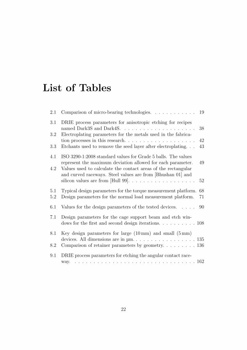
List of Tables
2.1 Comparison of micro-bearing technologies. . . . . . . . . . . . 19
3.1 DRIE process parameters for anisotropic etching for recipesnamed Dark3S and Dark4S. . . . . . . . . . . . . . . . . . . . 38
3.2 Electroplating parameters for the metals used in the fabrica-tion processes in this research. . . . . . . . . . . . . . . . . . . 42
3.3 Etchants used to remove the seed layer after electroplating. . . 43
4.1 ISO 3290-1:2008 standard values for Grade 5 balls. The valuesrepresent the maximum deviation allowed for each parameter. 49
4.2 Values used to calculate the contact areas of the rectangularand curved raceways. Steel values are from [Bhushan 01] andsilicon values are from [Hull 99]. . . . . . . . . . . . . . . . . . 52
5.1 Typical design parameters for the torque measurement platform. 685.2 Design parameters for the normal load measurement platform. 71
6.1 Values for the design parameters of the tested devices. . . . . 90
7.1 Design parameters for the cage support beam and etch win-dows for the first and second design iterations. . . . . . . . . . 108
8.1 Key design parameters for large (10 mm) and small (5 mm)devices. All dimensions are in µm. . . . . . . . . . . . . . . . . 135
8.2 Comparison of retainer parameters by geometry. . . . . . . . . 136
9.1 DRIE process parameters for etching the angular contact race-way. . . . . . . . . . . . . . . . . . . . . . . . . . . . . . . . . 162
22

Nomenclature
Symbols Used - In Order of Appearance
D Ball diameter
νSi Poisson Ratio Silicon
νSt Poisson Ratio 440C Steel
ESi Young’s Modulus Silicon
ESt Young’s Modulus 440C Steel
r Raceway curvature radius
W Force on the rolling element
dm Bearing Pitch Diameter
E Contact Modulus
R Ball Radius
a Elliptical Contact along Major Axis, or radius for point contact
b Elliptical Contact along Minor Axis
p0 Maximum Pressure at Center of a Contact Ellipse
σρ Geometric Parameter for Calculating Elliptical contacts
Pd Diametral Clearance
do Outer Diameter of Ball Raceway
di Inner Diameter of Ball Raceway
F% Raceway Fill
Nb Number of Balls in Bearing Design
23
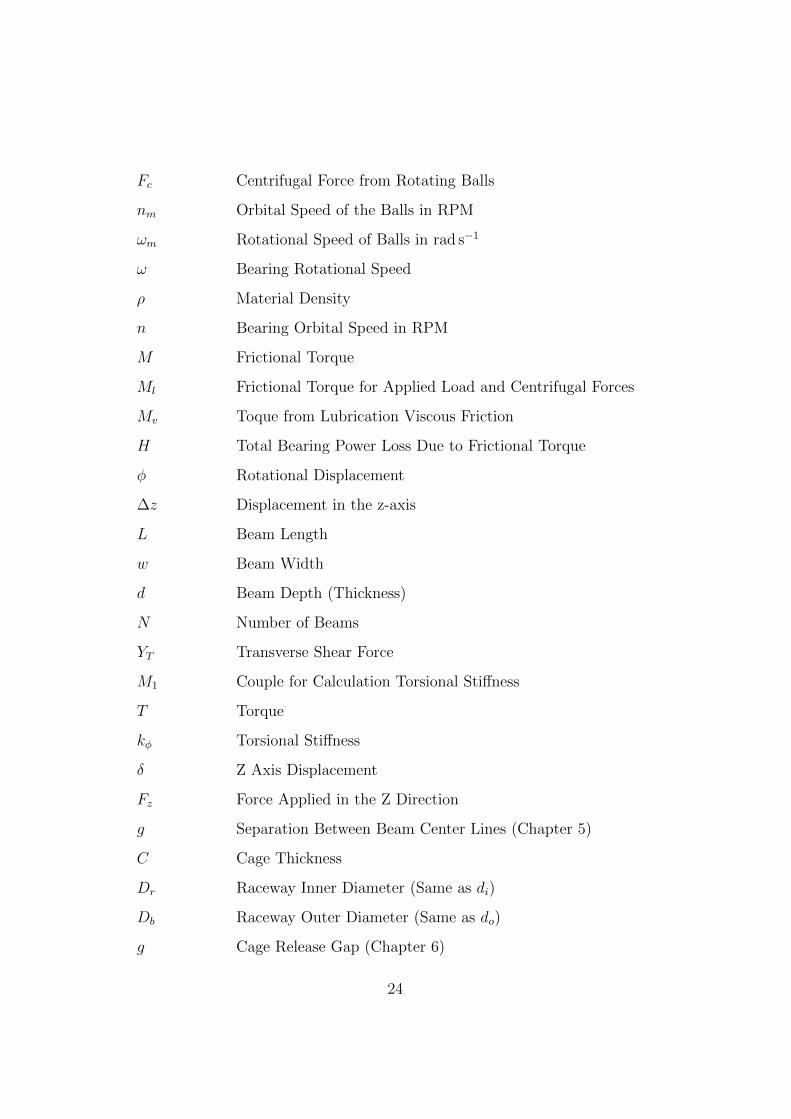
Fc Centrifugal Force from Rotating Balls
nm Orbital Speed of the Balls in RPM
ωm Rotational Speed of Balls in rad s−1
ω Bearing Rotational Speed
ρ Material Density
n Bearing Orbital Speed in RPM
M Frictional Torque
Ml Frictional Torque for Applied Load and Centrifugal Forces
Mv Toque from Lubrication Viscous Friction
H Total Bearing Power Loss Due to Frictional Torque
φ Rotational Displacement
∆z Displacement in the z-axis
L Beam Length
w Beam Width
d Beam Depth (Thickness)
N Number of Beams
YT Transverse Shear Force
M1 Couple for Calculation Torsional Stiffness
T Torque
kφ Torsional Stiffness
δ Z Axis Displacement
Fz Force Applied in the Z Direction
g Separation Between Beam Center Lines (Chapter 5)
C Cage Thickness
Dr Raceway Inner Diameter (Same as di)
Db Raceway Outer Diameter (Same as do)
g Cage Release Gap (Chapter 6)
24

t Raceway Tolerance Equal to 0.5PdWb Sacrificial Beam Width
Ww Etch Window Width
Hw Etch Window Height
RBP Radius of Ball Path
RI Retainer Inner Radius
RO Retainer Outer Radius
g Ball Pocket Opening (Chapter 8)
RB Ball Radius
RP Pocket Radius in Retainer
WBR Width of Bearing Raceway
WRR Width of Retainer Raceway
HBR Height of Bearing Raceway
HRR Height of Retainer Raceway (Incl. Solder)
HSO Stand-Off Height
HR Height of Retainer
δ± Radial Play in Retainer Ball Pocket
Acronyms
ADC Analog to Digital Converter
APC Automatic Pressure Control
BR Ball Riding (Cage Design)
BCB Bisbenzocyclotene
CAD Computer Aided Design
COF Coefficient of Friction
DRIE Deep Reactive Ion Etching
25

DSP Double Side Polished
HF Hydroflouric Acid
ICP Inductively Coupled Plasma
IRL Inner Ring Land (Cage Design)
KOH Potassium Hydroxide
MEMS Micro-Electro Mechanical Systems
ORL Outer Ring Land (Cage Design)
RF Radio Frequency
RIE Reactive Ion Etching
RPM Revolutions per minute
RF Radio Frequency
SEM Scanning Electron Microscope
SMT Silicon Micro-Turbine
SPI Serial Peripheral Interface
USB Universal Serial Buss
UV Ultra Violet
26
Chapter 1
Introduction
This chapter presents a brief background of MEMS bearings, the motivation
for performing the present work, and a list of objectives. The layout of the
thesis and a brief description of each chapter are also presented.
1.1 Background
The development of microengineered bearings capable of long-term operation
would open up new applications for MEMS technology, particularly in the
areas of micropower generation and microfluidics. Research on micro-scale
bearings dates back to the late 1980s when the first silicon rotary microma-
chines were demonstrated [Mehregany 90]. These devices had simple journal
or thrust bearings with sliding silicon contacts which showed high rates of
friction and wear. Subsequent research on bearings of this type focused on
the use of self-assembled monolayers [Maboudian 00] and dry coatings such
as diamond-like carbon [Smallwood 06] to reduce sliding friction; however,
such coatings suffer from degradation under load and do not allow long-
term operation. More recently attention has turned to vapour- [Asay 08]
and liquid-phase [Ku 12] lubrication methods for high-sliding contacts as
these allow replenishment of the lubricant. Recently a liquid bearing was
reported [Chan 11] which has a simple design and does not require exter-
nal controls, but the performance is highly reliant on the thickness of the
27

1.1 Background
fluid film in the bearing and this design could be difficult to encapsulate
into a working MEMS device. In parallel with the above, levitation schemes
based on electrostatic, magnetic or hydrostatic forces have been developed
as presented in [Houlihan 02], [Komori 01], and [Livermore 04]. These are
highly effective but require relatively complex control systems and an aux-
iliary supply of pressurised fluid or electrical power. Aerodynamic bearings
as demonstrated in [Frechette 05] and [Lin 99] avoid this control complexity
but can be made to work only at extremely high rotation speeds and have a
very complex mechanical design.
Microengineered rolling element bearings, such as those presented in this
thesis, could provide a viable alternative to the above approaches for applica-
tions involving low or moderate rotation speeds (up to around 50 000 RPM).
Rolling element bearings achieve low friction and wear by reducing the de-
gree of sliding at the load-bearing contacts; moreover they do not require
any external control system or power supply and they can operate over a rel-
atively wide range of speeds. Silicon MEMS rolling element micro-bearings
have been under development since the mid 1990s, and in the last few years
this technology has matured to the point where micro-ball bearings can be
integrated into functional devices (see, for example [Waits 10]). The bearing
raceways in these devices are formed by etching annular channels in a pair
of silicon wafers. The micro-balls (typically stainless steel) are placed manu-
ally in the raceway channels on one wafer before the two wafers are bonded
together; a final release etch is then used to free the moving part (inner ring)
of the bearing.
This thesis extends the exploration of silicon MEMS micro-ball bearings
in several new directions. The first is the integration of ball cage designs
into devices with micro-ball bearings. Ball cages are used in macro-scale ball
bearings to reduce friction, reduce the number of balls required, eliminate
ball-to-ball collisions, and increase the stability of the bearing. This work is
the first to explore the design and characteristics of ball cages in micro-scale
bearings. A further micro-ball bearing improvement explored in this work is
the fabrication of a curved ball race. This is also a common design aspect
in macro-scale ball bearings and allows for the creation of self-centering and
28

1.2 Motivation and Goals
angular contact ball bearings. The new bearing designs were fabricated and
then tested using an existing micro-turbine design and a micro-tribometer
for studying high-sliding contact MEMS devices. The ultimate goal of these
micro-ball bearing design changes is to provide a platform for designing reli-
able and stable rotary MEMS bearings that can be incorporated into devices
such as micro- pumps, gears and generators.
1.2 Motivation and Goals
The motivation behind this research was to explore the possibility of trans-
ferring common aspects found in macro-scale ball bearings to the design of
micro-ball bearings, thereby creating a platform for designing reliable rotary
devices for micro-scale applications. The primary goal was to introduce new
design and fabrication techniques with broader applications in micro- motors,
gears and pumps that will open new possibilities in the design of devices for
the space, medical and mechanical engineering fields. This would bring the
MEMS field closer to reaching the goal of achieving highly reliable micro-scale
rotary devices.
1.3 Research Objectives
The aim of the project described in this thesis was to explore the integration
of new geometries and fabrication techniques into the design of micro-ball
bearings. The following tasks were performed during this exploration:
1. Characterize the performance of the devices designed for this study by
modifying and improving, where possible, existing testing methodolo-
gies (Chapter 5.)
2. Design and integrate a ball cage into a MEMS micro-ball bearing using
the simplest technique possible (Chapter 6.)
3. Design a fabrication technique for releasing moving parts from MEMS
devices with multiple layers (Chapter 7.)
29

1.4 Description of Thesis
4. Integrate a ball cage into a working MEMS device with a micro-ball
bearing support mechanism (Chapter 8.)
5. Create a micro-ball bearing raceway with a curved geometry that will
allow for the bearing to self-center and to better mimic race geometries
found in conventional macro-scale bearings (Chapter 9.)
The aim of studying these bearing designs and geometries was to deter-
mine the feasibility of modifying the design and fabrication of micro-bearings
to incorporate features commonly found in macro-scale bearings. Further the
study was intended to determine of how these new designs affected the per-
formance of the bearing designs. Though the new geometries explored here
are not ideal for all micro-rotary applications, the designs presented have
shown that it is possible to integrate many aspects of macro-scale bearings
into the design of micro-scale bearings.
1.4 Description of Thesis
The remainder of this thesis is organised as follows:
Chapter 2: Bearings in MEMS Devices - Presents competing MEMS
bearing technologies and previous work on MEMS micro-ball bearings.
Chapter 3: Micro-fabrication Techniques and Constraints - De-
scribes the micro-fabrication techniques used to create the devices described
in this thesis.
Chapter 4: Ball Bearing Design Consideration and Tribology - De-
scribes the ball bearing design and tribological considerations important to
the study presented in this thesis.
Chapter 5: Testing Methodologies - Describes the techniques used to
characterize the devices created for this study.
30

1.4 Description of Thesis
Chapter 6: Proof of Concept of a Radial Ball Bearing with In-
tegrated Ball Cage - Describes the fabrication and performance of the
device with the simplest cage integration technique.
Chapter 7: In-Situ Fabrication of a Monolithic Silicon Ball Cage -
Presents a new and novel technique for releasing moving silicon structures in
devices made from stacking multiple wafers.
Chapter 8: Micro-Turbines with Integrated Silicon Ball Cage -
Presents and compares 5 cage designs that were integrated into an exist-
ing micro-turbine device.
Chapter 9: Curved Raceway - Presents the integration of a curved race-
way geometry, made with deep isotropic etching, into micro-ball bearings.
Chapter 10: Conclusions and Further Work - Presents the conclu-
sions of the studies in this thesis and proposes suggestions for further work.
Bibliography Contains a full list of references cited in this thesis.
31

Chapter 2
Bearings in MEMS Devices
Several MEMS bearings technologies have been explored over the years. This
chapter will present several of the competing technologies that have emerged
along with previous work on micro-ball bearings.
2.1 Competing Bearing Technologies
Research on micro-scale bearings has been reported since the late 1980s. This
section will provide an overview of the dominant micro-bearing technologies
that compete with micro-ball bearings in the design of rotary MEMS devices.
Table 2.1 presents a comparison of the technologies presented in this section,
including micro-ball bearings.
Technology Design Speeds Load Stability ExternalComplexity Cap. Control
Pin Joint Medium Low-Medium Low High NoneMag. Lev. High Medium-High Low Low Complex
Jewel Low Low-High Medium Medium NoneAir High High Low Low Complex
Liquid Medium Low Low Low NoneMicro-Ball Low Low-Medium High High None
Table 2.1: Comparison of micro-bearing technologies.
32

2.2 Pin Joint Bearing
2.2 Pin Joint Bearing
One of the earliest reported rotary MEMS bearings was the pin joint bearing.
In this design the rotor is fabricated around a ”pin” that is attached to the
stator. A cap is then fabricated on the top of the pin to keep the rotor in
place. A typical fabrication technique was to fabricate the rotor in polysilicon
on a sacrificial silicon dioxide layer as seen in [Mehregany 98] and [Garcia 95].
However the use of thick metal layers to form the bearing structures with a
PMMA sacrificial layer has also been reported in [Guckel 98]. This design
can only support very low loads due to the large surface area of the contacts
at the interface of rotor and stator. The contact surface area limits the
load due to the fact that high loads will cause the friction and wear at the
interface to increase dramatically. The effects of wear have been observed
in several applications using the pin joint bearing. In [Mehregany 90] it was
found that the performance of a wobble motor increased over time due to
wear increasing the bearing clearance; however, it was also observed that
the particles from this wear process could seize the bearing. In this study
no devices failed due to failure of the pin or the joint structures. Further,
the observation of excessive wear causing failure due to rotor misalignment,
making it impossible to actuate the device, in micro- turbines and gears after
around 1 million revolutions was reported in [Gabriel 90].
Sandia National Labs has performed the most extensive tests of polysil-
icon pin joint structures with a rotor actuated by a set of capacitive linear
drives connected by a pin joint bearing. In [Garcia 95], it was shown that a
silicon nitride on polysilicon joint was superior to a polysilicon on polysilicon
one. This was attributed to the formation at fewer particulates and improved
tribological characteristics at the polysilicon to silicon nitride interface. The
improved device was observed to survive over 2.8 million cycles at 1500 RPM.
These devices also suffered from seizure due to wear particles collecting at
the bearing interface. A further characterization of the failure modes of these
devices, presented in [Miller 97], seems to indicate that asperities formed be-
tween sliding contacts cause sticking and ultimately failure in the motors.
In other work [Paterson 97], it was difficult to observe wear on the bearing
33

2.2 Pin Joint Bearing
contacts with SEM imaging and it was considered that failure modes often
had more to do with electrostatics or drive failures, rather than failures in
the bearing. A later study on loaded gears [Tanner 98] did show that the
dominant failure mode in this type of bearing was in fact due to wear at
the bearing interfaces. These results were further reported in [Tanner 00]
and [van Spengen 03]. Figure 2.1 shows the design of the gear and the wear
observed at the bearing interfaces. Later it was determined [Tanner 02] that
the dominant design parameter for increasing the longevity of the bearing was
an increased gap spacing in the bearing which reduces the contact time and
friction between the rotor and stator hence reducing wear. The reduced wear
also reduces the generation of particles that can seize the bearing and the
loss of materials from the rotor a stator surfaces that can lead the ultimate
mechanical failure of the parts.
Figure 2.1: A. Image of the gear arrangement in the polysilicon pin jointstudies; B. Excessive wear found on drive gear pin hole; C. Undamaged pinhole on side gear to compare with above image; D. Cross section of the pinjoint bearing interface showing unworn structure (top) and worn structures(bottom). Images reproduced from [Tanner 98]
34

2.3 Magnetic or Electrostatic Levitation
2.3 Magnetic or Electrostatic Levitation
Magnetic and electrostatic levitation seem to be very compelling technolo-
gies for use in MEMS devices. With the low loads and forces experienced
at the micro-scale levitation should be able to provide a reliable low friction
bearing. The major challenges to using this technology, however, are incor-
porating permanent magnetic materials into the fabrication process (though
this can be accomplished manually) or incorporating the control system re-
quired to keep the rotor suspended and stable during rotary operation. Ex-
amples of magnetic levitation systems in MEMS are described in [Komori 01]
and [Houlihan 02]. These devices operate best at moderate to high speeds,
and though the technology has been proven to be conceptually sound it has
not received widespread acceptance as a MEMS bearing technology. A less
complex method used to electrostatically levitate a simple proof mass in a
power harvesting application has also been shown to be effective in elimi-
nating stiction in [Suzuki 10]. Electrostatic levitation has also been demon-
strated in MEMS gyroscopes in by using planar coils to levitate and stabilize
an aluminium rotor as reported in [Williams 96] and [Shearwood 00]. This
micro-motor was able to reach speeds of approximately 1000 RPM in air and
was tested at to over 200 hours with no indication of degradation in per-
formance. A final promising approach to creating levitation bearing is the
use of diamagnetic levitation. This method uses static fields that require no
external controls. A proof of concept design for a levitated accelerometer is
presented in [Garmire 07] and a capacitive drive micro-motor is presented
in [Liu 08]. A model for improving the performance of MEMS accelerome-
ters using this technique is presented in [Pasquale 09]. Though these initial
results are encouraging for broader application of this technique, there is no
evidence yet of a fully integrated MEMS system using this technology.
2.4 Jewel Bearing
The jewel bearing has been widely used in watch making for centuries. This
simple bearing requires only a pair of hard, smooth, cupped surfaces (jewels)
35

2.5 Air Bearing
placed on stator platforms above and below a pin attached to the rotor. A
conceptual drawing of this design is shown in Figure 2.2. This is a relatively
simple design but requires at least 3 surfaces in order to work properly, which
could increase the complexity of MEMS device design. The three surfaces
involved would be the top jewel surface (stator), the rotating device in the
center (rotor) and the bottom jewel surface (stator.) This design also can
allow wobble and instability that is unfavourable in some MEMS applications.
However, the simple design, wide range of acceptable speeds, low wear, and
lack of external controls make this an attractive bearing technology. Some
examples of this application in MEMS and centimeter scale applications can
be found in [Lee 05], [Leinvuo 06], [Romero 09] and [Bansal 09].
Figure 2.2: Conceptual drawing of a common jewel bearing design, withjewels forming a cup on the stator to hold a pin attached to the rotor.
2.5 Air Bearing
High-speed micro-turbines supported on an air bearing were first explored in
the late 1990s by Massachusetts Institute of Technology. The stability of this
type of bearing relies on carefully controlling the air pressure at several points
in the device. Hydrostatic thrust bearings levitate the rotor at the center.
Journal bearings at the periphery of the rotor are needed to keep the rotor
36

2.5 Air Bearing
from colliding with the stator during rotation. A thrust plenum balance is
needed to keep the bottom of the rotor from colliding with the stator under
load. And finally there is the main inlet pressure which drives the turbine.
Figure 2.3 shows the cross section of a silicon micro-turbine supported by
an air bearing. Disadvantages of this approach are the complexity of the
bearing design (requiring a 5 wafer stack), the need for closed loop control
(the stability of the bearing is highly dependent on maintaining tight control
over, and balancing, the air pressures in the device), and the fact that the
rotor must necessarily collide with the stator when the air pressure is removed
from the device.
Figure 2.3: Optical photograph (top) and schematic (bottom) of the crosssection of a silicon micro-turbine supported on an air bearing. Diagramreproduced from [Frechette 05].
In the first reported results for a device of the type shown in Figure 2.3,
in [Lin 99], the turbine was able to achieve speeds of up to 60 000 RPM. The
upper speed and stable operation of the bearing were limited by the stiffness
of the air bearing, and it was difficult to maintain rotation without the rotor
touching down on the stator. With fabrication improvements and optimiza-
tion of the bearing stiffness speeds of up to 1 400 000 RPM were achieved
37

2.5 Air Bearing
and reported in [Frechette 00]. In [Frechette 05], it is reported that several
of the devices were still limited to speeds below 60 000 RPM, and all of the
devices (high and low speed) could suffer from catastrophic failures typically
attributed to rotor instability. The need for highly stable and precisely fab-
ricated rotors required extensive optimization of the fabrication parameters,
with special emphasis on the DRIE (deep reactive ion etching) processes.
A further exploration of the DRIE optimization and tight fabrication toler-
ances is reported in [Kang 05] for a similar device used to explore MEMS
turbochargers. Another study, [Hara 03], explored 3 types of journal bearing
structures, finding that an asymmetrical multi-lobed journal bearing would
be the best candidate for high-speed turbine operation. It was also observed
that the air bearing operated in 3 distinct modes, as shown in Figure 2.4.
Mode C is the most desirable mode due the fact that contact is made at the
journal bearing and not at the top or bottom surface of the rotor allowing
for the most stability and freedom of movement. Further in this mode only
the journal pressure will need to optimized to compensate for the centrifugal
forces.
Work on creating working MEMS engines and generators struggled pri-
marily with the rotor dynamics and operation of the air bearing support
mechanism [Epstein 04]. Integration of inductive coils needed to create a gen-
erator or motor from these devices has been demonstrated in [Livermore 04].
However, optimization of the bearing stability and control still limit the ap-
plication of this type of bearing.
38

2.6 Liquid Bearing
Figure 2.4: Air bearing operating modes presented in [Hara 03]. Figurereproduced from [Hara 03].
2.6 Liquid Bearing
A recent exploration of liquid bearings is presented in [Chan 11]. This bear-
ing uses water or ethylene glycol as the bearing support mechanism. A
hydrophobic (Cytop) layer is used to keep the bearing in a fixed location.
This technique relies on the surface tension of the liquid to support the ro-
tor of the device, making drag and load capacity dependent on the liquid
film thickness. The results reported show a drag reduction of over 15 times
compared to micro-ball bearing designs of similar dimensions. It is unclear,
however, how a fully encapsulated liquid bearing could be incorporated into
a MEMS device as the liquid would have to integrated into the device at
39

2.7 Previous Work in Micro-Ball Bearings
some point in the fabrication process and would have to be maintained at
the rotor and stator interfaces. This design method is attractive because it
requires no external control mechanisms and provides the reduced drag and
friction of air bearings with much less design complexity.
2.7 Previous Work in Micro-Ball Bearings
MEMS micro-ball bearings have been under investigation by the University
of Maryland since the late 1990s. Bearing manufacturers have also been pro-
viding micro-ball bearings, fabricated through more conventional methods,
for many years. This section will present an overview of the MEMS micro-
ball bearing research and will also some details on commercially available
micro-ball bearings.
2.7.1 Linear Micro-Ball Bearing
Linear ball bearings were the first type used to characterize micro-ball bear-
ing performance in MEMS devices, the first resuts appearing in the early
2000’s with [Lin 01] and [Lin 02]. In [Lin 04] linear bearings with V-groove
raceways, created by isotropic KOH etching, were studied in-situ using a
visual processing technique to measure the displacement of the slider in re-
lation to the stator. This first investigation showed a significant reduction in
the COF (coefficient of friction) between structures with micro-ball bearings
in relation to those with sliding contacts. The same system was also used to
further characterize the hysteresis present in this linear bearing system, as
described in [Tan 04]. A further study, leading to the development of a model
for the friction and hysteresis observed in the linear micro-ball bearings, was
presented in [Tan 06a].
40

2.7 Previous Work in Micro-Ball Bearings
Figure 2.5: (a) Schematic of the linear micro-motor on micro-ball bearings(b) Square wave motor drive signal. Figure reproduced from [Modafe 06].
A linear bearing was first integrated with an electrostatically driven micro-
motor in [Modafe 06]. The bearing grooves had straight side walls, fabricated
with DRIE, rather than the V-grooves used in earlier work due to an incom-
patibility between the KOH etching needed to create the V-grooves and the
thick BCB used for electrical isolation in the electrostatic drive. Figure 2.5
shows a diagram of the linear electrostatic motor with the square wave driv-
ing signals. This device did perform as predicted when allowance was made
for flaws relating to the fabrication process. A better agreement with theory
was reported in [Ghalichechian 07]. Due to this understanding and charac-
terization of dynamics of the bearing, a closed loop control system could be
41

2.7 Previous Work in Micro-Ball Bearings
integrated into the linear motor that provided positional control with a reso-
lution of 120 µm over a total travel of 2 mm, as reported in [Beyaz 09]. This
work provided initial confirmation of the performance and controllability of
MEMS devices supported on micro-ball bearings.
2.7.2 Rotary Micro-Ball Bearings
The first exploration of a rotary micro-ball bearing was reported in [Waits 07a].
This was a simple bearing integrated into a square chip. The device was ac-
tuated by placing the outer corners of the device die into a flow of pressurized
nitrogen. This first bearing suffered from ball jamming, extensive wear at the
bonded wafer interface and wear on the steel balls, as shown in Figure 2.6.
This design was further refined to produce a 6-phase capacitive micro-motor
(similar in design to the linear motors mentioned in the previous section), as
reported in [Ghalichechian 08]. These experiments showed that the perfor-
mance of the bearing was in agreement with the previously developed models
and proved that micro-ball bearings could be integrated and encapsulated for
use in MEMS devices.
Further research involved integrating the micro-ball bearing into devices
with micro-turbines in the rotor. The first turbine designs used a tangential
flow to drive the turbine, see [Waits 07b]. This turbine still suffered from poor
performance. A dramatic improvement in performance was realized when
the turbine design was changed and the ball bearing raceway contact surface
was changed to more closely resemble that of a thrust bearing, as shown in
[McCarthy 09], reducing friction and wear. Moving the bond interface away
from the center of the ball to reduce the wear at the bond interface increased
the longevity and performance of the bearing, as reported in [Hanrahan 10].
These changes have finally enabled the micro-ball bearing to achieve a level
of reliability and performance acceptable for integration into Power MEMS
devices. Recently magnets and coils have been integrated into the SMT
device for power generation [Beyaz 10].
42

2.7 Previous Work in Micro-Ball Bearings
Figure 2.6: A. Optical image of ball jamming in the bearing raceway; B. SEMimage of ball without wear (top) and ball after 39 min. operation (bottom);C. SEM image of the unworn bonded silicon raceway interface (top) and theworn bonded silicon raceway interface. Images reproduced from [Waits 07a].
2.7.3 Conventional Micro-Ball Bearings
Conventional or commercially available micro-ball bearings require special
manufacturing techniques, equipment and hand assembly. The manufactur-
ing process can take between 8-12 weeks and must meet extremely tight tol-
erances. These bearings can be found in applications such as medical pumps,
dentist drills, aerospace applications, watches and office equipment [Mc-
Cann 09]. The complex manufacturing process could benefit from the batch
fabrication techniques made available by using silicon as the raceway mate-
rial, thereby reducing the overall time and cost of production. The extremely
tight tolerance required for these bearings can also be met easily with the
43

2.7 Previous Work in Micro-Ball Bearings
fabrication techniques proposed in this and other MEMS micro-ball bearing
research.
As an example of a commercially available ball bearing, one part listed by
NSK Micro Precision Co., has an inner diameter of 0.6 mm, outer diameter
of 2 mm, and a ball diameter of 0.3 mm [NSK 12]. NMB Technologies Corpo-
ration list a bearing with an outer diameter of 1.5 mm, inner bore of 0.5 mm
and a ball diameter of 0.25 mm [NMB 12]. MPS, a member company of the
Faulhaber Group, lists a bearing with an outer diameter of 1.6 mm, inner
diameter of 0.3 mm, and ball diameter of 0.2 mm [MPS 12b]. MPS provides
a large selection of micro-bearings for watches, medical equipment and other
applications. The Timken S100 ball bearing, pictured in Figure 2.7, has an
outer diameter of 2.5 mm, an inner diameter of 0.6 mm and a ball diameter
of 0.6 mm. Information on Timken bearings and applications can be located
at [Timken 12].
Figure 2.7: Picture of the Timken S100 micro-ball bearing, photo by TimkenCo.
44

2.8 Discussion and Conclusions
2.8 Discussion and Conclusions
Several bearing technologies have been proposed and tested for MEMS sys-
tems. Many of these techniques have limitations that would make them
unacceptable for harsh environments or suffer from catastrophic failure over
a short period of time. The pin joint bearing can only support light loads and
fails due to wear at the rotor and stator/pin interface. Magnetic and elec-
trostatic levitation bearing also support low loads and can require complex
external controls. Though the use of diamagnetic materials could lead to lev-
itation bearings that do not require any external controls the technique has
not yet been demonstrated in a fully integrated system. Jewel bearings could
provide a stable and low friction bearing with a long service life, however,
this design has not yet been integrated in a MEMS device. Air bearings also
offer a low friction bearing, but only work at higher speeds and suffer from
low stability that can only be overcome with complex designs and external
control systems. And finally, the liquid bearing which can also only support
low loads and have not yet been fully integrated into a MEMS system.
Micro-ball bearings show a high stability over a wide range of operating
speeds and applied loads with no external controls. The mechanical support
in the bearing also allows devices to survive shock and vibration during op-
eration that would cause catastrophic failures in several of the other bearing
designs. The initial results have indicated that this low complexity design
has broad application in rotary and linear MEMS actuators. Ball co-location,
which resulted in the seizure of the bearing, was a problem in the early micro-
ball bearing designs. The research this thesis will explore the use of ball
cages or retainers, common in macro-scale bearings, to solve this problem.
Further, a curved raceway will also be presented that will more closely match
the geometry found in macro-scale ball bearings and allows the bearing to
self-centre during operation. These improvements are intended to improve
the longevity and performance of the bearings in MEMS applications.
45

Chapter 3
Micro-Fabrication Technologies
This chapter will outline the micro-fabrication techniques used to make the
devices described in this thesis. A brief and general description of each tech-
nique will be presented with an explanation of the constraints of the technique
as applied to this research. It should be noted that the techniques used were
often chosen due to the availability of suitable equipment in our laboratory
and not always because they were the first choice for accomplishing the step.
Therefore, process and device design should be considered in the light of
the restrictions of the processes described in this chapter. These restrictions
inevitably lead to added complexity in some of the processing described in
later chapters.
3.1 Patterning and Masking
The first step in a MEMS fabrication process involves creating a set of masks
with the patterns required to define the desired device. The patterns on the
masks are transferred to the substrate at different stages in the process flow
using a photolithographic process. In the research described in this thesis
all masks were created with 1:1 scale and the patterns transferred using a
contact mask aligner. Other techniques such as proximity printing, projec-
tion and stepper printing were not used. For a more detailed description
of photolithographic processes and technologies the reader is encouraged to
46

3.1 Patterning and Masking
review Chapter 2 in [Jaeger 02].
3.1.1 Photo-Masks
Two types of masks were used for the photolithography process: chrome/glass
and polymer. Chrome/glass masks are made from a soda lime glass with
a thin (typically 980 A) layer of chrome which is patterned by direct-write
lithography using either a laser or electron beam. These masks provide a high
resolution, and are durable and easy to clean. The chrome/glass masks used
in this work were printed by Delta Mask [DeltaMask 12] and had a printable
resolution of 1 µm. In order to explore multiple designs, and to create the
more complex multiple-mask designs at a lower cost, polymer masks were also
used. These masks were printed by JD Photo-Tools [JDPhoto 12], with a
photo-emulsion film on a polyester-based film. These masks must be handled
carefully because the emulsion film is soft and easy to scratch and cannot be
cleaned. The resolution of the masks can be as fine as 8 µm; however, they
can exhibit dimensional instability under varying humidity and temperature
conditions. The key advantage of polymer masks is that 24 masks for 100 mm
diameter wafers can be printed for the same cost as 1 chrome/glass mask.
3.1.2 Photolithography
Photolithography is the process of transferring the pattern from the mask to
a layer of photoresist on the substrate. In a mask aligner this is accomplished
by aligning the mask to features on the substrate with the aid of a micro-
scope, bringing the mask and substrate into contact, and then exposing the
photoresist to UV (ultra violet) light incident through the mask. The expo-
sure step produces a latent image in the photoresist layer which is converted
to a topographic pattern when the wafer is immersed in a developer solution.
There are two common types of photoresist: positive and negative. In
a negative resist the UV exposure results in cross-linking of the photoresist
making it less soluble in developer. While in positive resists the UV exposure
makes the photoresist more soluble in the developer. Therefore, after devel-
opment, negative resists will remain in regions corresponding to the clear
47
3.1 Patterning and Masking
areas of the mask, while positive resist will remain in regions corresponding
to the dark areas [May 06]. For this research positive photoresist was used
for all pattern transfer.
3.1.3 Masking Materials
Two types of masking materials were used for the processes described in this
thesis. Photoresist was used to define regions for electroplating, RIE (reactive
ion etching) of silicon dioxide and DRIE of silicon, while silicon dioxide was
used as an alternative mask material for RIE and DRIE etching of silicon.
These masking material will be described in the following sections.
3.1.3.1 Photoresist
Photoresist is used to transfer the mask pattern to the substrate for sub-
sequent processing. For the fabrication processes described in this thesis, a
thick photoresist was required that could survive highly aggressive etching
and also act as a template or mold for thick (>1 µm) metal electro-plating.
For all of these steps it was easiest to use one type of photoresist with an
optimized process for our specific laboratory equipment. As a result it was
determined that AZ9260 was the ideal photoresist for all of processes used
to fabricate the devices. This resist can be used to create thick coatings, and
it has a very high resistance to plasma etching (with selectivity of at least
80:1 observed in DRIE etching) as well as a high resistance to electroplating
bath chemistry; it also provides excellent photo-patterning capabilities. A
guide on recommended processing steps for AZ9260 positive photoresist can
be found in [MicroChemicals 09]. The standard process used for AZ9260 in
this thesis was provided by Dr. Werner Karl [Karl 08] and was optimized
to provide a coating with a thickness of approximately 10 µm on the equip-
ment in the laboratory. Some minor optimizations were made to the coating
process over time to improve throughput and reduce processing time when
applying photoresist to multiple substrates. The AZ9260 coating process is
detailed in Appendix A.
48
3.1 Patterning and Masking
3.1.3.2 Silicon Dioxide
Silicon dioxide was used as a resilient hard mask for several DRIE processing
steps. Some of the advantages of silicon dioxide as a masking material are:
1. It can be grown on silicon by thermal oxidation. (A 1 µm layer can be
grown in an oxidation furnace at 1100 ◦C, with 1 l min−1 Oxygen flow,
for 48 h.)
2. It is able to survive high temperature processing.
3. It is unaffected by, or minimally affected by, most chemistry used in
other processing steps (i.e. metal etching with acids, electroplating
bath chemistry, photoresist stripping).
4. It offers high selectivity against silicon during RIE and DRIE process-
ing, with a slectivity of 50:1 observed during DRIE etching.
5. It can be patterned by depositing a photoresist mask then etching the
exposed oxide using HF wet etching or RIE dry etching. Mask resolu-
tion is limited only by the oxide thickness, the anisotropy of the etch
process and the resolution of the photoresist mask.
In the process flow of the devices described in this thesis, a silicon dioxide
mask is used during the final etching step. This is due to the fact that the
mask can be defined on the wafer before it is broken into die for assembly.
The hard mask can then survive handling, assembly and the high temperature
wafer bonding. Different layers of silicon dioxide, photoresist and exposed
silicon are also used in some processes to create stepped geometries in the
silicon substrate.
The silicon dioxide masks used in this thesis were created by first defining
a mask in AZ9260 and then transferring the pattern into the oxide by reactive
ion etching the exposed silicon dioxide using an Oxford Instruments System
80 etch tool. The basic theory behind plasma etching can be found in Section
2.1.3.2 of [May 06]. In this process we used CHF3 to create the etchant
species in the plasma. Due to a characterization of the etching processes
49

3.2 Deep Reaction Ion Etching (DRIE)
found in [Kumar 07], it was determined that 2 min etch steps should be
interspersed with 2 min cooling steps. This prevents resist damage induced
by overheating during the etching process. This process provided excellent
pattern transfer from AZ9260 mask to the oxide layer. Minimal undercut
was observed and the photoresist patterns transferred within the required
design tolerances. It was also determined that HF wet etching of the oxide
would not provide the desired pattern resolution.
3.2 Deep Reaction Ion Etching (DRIE)
Deep Reactive Ion Etching (DRIE) is one of the key processes that has made
this research possible. The DRIE process used for this research was the Bosch
process, described below. Therefore all references DRIE in other sections of
this thesis are referring to the Bosch process. This process allows for creat-
ing high aspect ratio, deep, anisotropic features in a silicon substrate. The
section will give a brief overview of the principles of this process, processing
considerations for through wafer etching, the use of halo masks to improve
etch uniformity in through wafer etching, and the effects of etch lag.
3.2.1 Basic Principles
The Bosch DRIE silicon etching process was used in this research to define
anisotropic trenches in the silicon substrates. Chapter 4 of [Kumar 07] has
an excellent overview of the processes, design considerations and equipment
used for the research presented here. The Bosch DRIE process achieves
deep anisotropic etching using a highly reactive gas to create a high density
plasma to etch the features in to the silicon while also interleaving passivation
steps that protect the sidewalls from isotropic etching. Due to the inherent
isotropic etching of the stable flourochemicals typically used in this process
a polymer passivation layer is required to protect the sidewalls of the feature
from the etchant species. In the Bosch process this is accomplished by time-
multiplexed or pulsed etching, in which the substrate is first etched and then
a passivation layer is deposited. [Schilp 96] An excellent overview of the Bosch
50

3.2 Deep Reaction Ion Etching (DRIE)
Parameter Dark3S Dark4SEtch Step (s) 11 13
Passivation Step (s) 8 6Etch Rate (µm min−1) 3 4
SF6 Flow Rate 130 sccmO2 Flow Rate 13 sccmC4F8 Flow Rage 85 sccm
RF power 600 WRF frequency 13.56 MHzPlaten Power 20 wattAPC setting 75% (manual)
Table 3.1: DRIE process parameters for anisotropic etching for recipes namedDark3S and Dark4S.
DRIE history and process considerations can also be found in [Laermer 10].
In this research a Surface Technologies Systems multiplex ICP etcher was
used for the DRIE processing. SF6 was used as the etchant gas and C4F8
was used to deposit the passivation layer. The recipes typically used for
the DRIE processes described in this thesis are presented in Table 3.1. The
Dark3S recipe has been optimized for etching 40 µm-wide features through
a wafer, and also performs well when all of the etched features are below
150 µm. Dark4S performs well for features larger than 150 µm, but does have
a tendency to create footing or widening of the trench as the etch depth
increases. The primary difference between the two recipes is the ratio of the
etch step to the passivation step. The etch rates given are typically valid
to a depth of approximately 250 µm, at which point the etch rate seems to
drop off markedly and at a rate that is highly dependent on the width of the
etched feature.
3.2.2 Through-Wafer Etching
One method used to create the test suspension and ball cages presented
in this research was to etch the structures from a silicon substrate. Etch
lag becomes a significant factor during through-wafer etching, where larger
features will etch at a higher rate than smaller features. This leads to the
51

3.2 Deep Reaction Ion Etching (DRIE)
need for using a halo mask design to ensure a near-constant etch rate for all
of the features on the wafer during a through-wafer etch. In [Pike 03] the
optimization of the DRIE etching parameters and mask design for through-
wafer etching are discussed. The results of these optimization studies were
used for through-wafer etching as presented in this thesis and also in [Ku 10b]
and [Kumar 07].
The basic concept of the process involves patterning resist on the sub-
strate with the desired features. The features are then etched to a depth
that is typically greater than half of the thickness of the substrate. The
substrate is then mounted on a backing wafer, typically a silicon substrate,
using photoresist as a temporary bonding adhesive. The features are then
etched the rest of the way through the substrate. The wafer stack is then
soaked in acetone or photoresist stripper to detach the backing wafer and to
remove any parts of the substrate that are no longer attached to the devices
as a result of the etching.
3.2.3 Halo Mask for Through Wafer Etching
In order to overcome the effects of etch lag while trying to remove significant
portions of silicon during a through-wafer etch a ”halo” mask can be used.
This type of mask is designed so that all of the features on the mask are of
similar width. Large areas of silicon that need to be removed from the device
are surrounded completely by a narrow trench so that they will drop out at
the end of the process. This technique is used in, for example [Bayt 98],
[Kumar 07], and [Pike 03]. Figure 3.1 shows the concept of this type of mask
design.
52

3.2 Deep Reaction Ion Etching (DRIE)
Figure 3.1: Halo mask concept (left) with the etch trenches in white, thedevice structure in pink and the sacrificial substrate in green. SEM (right)of a device fabricated by through wafer etching using a halo mask.
3.2.4 Etch Lag
DRIE etch lag is an important factor that must be considered when designing
devices that rely heavily on the geometries of high aspect ratio anisotropic
trenches. Features with different widths will etch at different rates during
DRIE processing. An illustration of this phenomenon is shown in Figure 3.2.
In [Chung 04] it is shown that, regardless of the trench shape, the etch rate
depends on the area of the trench. This effect is primarily due to ion and radi-
cal or inhibitor depletion during the DRIE process [Gottscho 92]. Differential
charging of insulators, field curvature near conductors, image force deflection,
and ion shadowing with ion angular distribution are responsible for ion deple-
tion. Radical/inhibitor shadowing, molecular flow, bulk diffusion and surface
diffusion are responsible for radical and inhibitor depletion [Jansen 97]. Op-
timization of DRIE parameters to accommodate differently sized high aspect
ratio features has been explored in [Ayon 01] and this effect has also been
used in the fabrication of 3-dimensional structures [Rao 04]. A model is also
available in [Tan 06b]for predicting and simulating the effects of etch lag.
53

3.3 Electroplating
Figure 3.2: SEM image of high aspect ratio silicon trenches, with featuresizes ranging from 2.2 µm on the left to 5.5 µm on the right. Larger trenchsizes have a higher etch rate and lower aspect ratio. Image from [Chung 04].
For many of the devices described in this thesis multiple DRIE steps
were used to create stepped profiles in the silicon substrate. The design of
the device features and etching process is further complicated, due to etch
lag, because as the stepped profile in the silicon is etched deeper the effects of
etch lag are enhanced on the narrower features patterned in the earlier layers.
This lag requires that the narrower and deep features must be initially etched
to a much greater depth in order to retain the desired final etch profile. A
further challenge in most of the designs presented in this thesis is that many
of the device features are of very different sizes. During some of the etching
processes trench widths can range from 40 µm to 510 µm. These factors are
critical considerations during the design of the masks and process flow for a
device.
3.3 Electroplating
Electroplating or electrodeposition of metals onto a substrate is a common
method of creating interconnects and depositing metals for wafer bonding
54
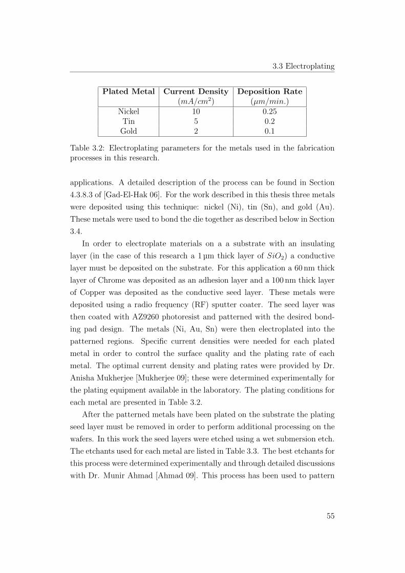
3.3 Electroplating
Plated Metal Current Density Deposition Rate(mA/cm2) (µm/min.)
Nickel 10 0.25Tin 5 0.2
Gold 2 0.1
Table 3.2: Electroplating parameters for the metals used in the fabricationprocesses in this research.
applications. A detailed description of the process can be found in Section
4.3.8.3 of [Gad-El-Hak 06]. For the work described in this thesis three metals
were deposited using this technique: nickel (Ni), tin (Sn), and gold (Au).
These metals were used to bond the die together as described below in Section
3.4.
In order to electroplate materials on a a substrate with an insulating
layer (in the case of this research a 1 µm thick layer of SiO2) a conductive
layer must be deposited on the substrate. For this application a 60 nm thick
layer of Chrome was deposited as an adhesion layer and a 100 nm thick layer
of Copper was deposited as the conductive seed layer. These metals were
deposited using a radio frequency (RF) sputter coater. The seed layer was
then coated with AZ9260 photoresist and patterned with the desired bond-
ing pad design. The metals (Ni, Au, Sn) were then electroplated into the
patterned regions. Specific current densities were needed for each plated
metal in order to control the surface quality and the plating rate of each
metal. The optimal current density and plating rates were provided by Dr.
Anisha Mukherjee [Mukherjee 09]; these were determined experimentally for
the plating equipment available in the laboratory. The plating conditions for
each metal are presented in Table 3.2.
After the patterned metals have been plated on the substrate the plating
seed layer must be removed in order to perform additional processing on the
wafers. In this work the seed layers were etched using a wet submersion etch.
The etchants used for each metal are listed in Table 3.3. The best etchants for
this process were determined experimentally and through detailed discussions
with Dr. Munir Ahmad [Ahmad 09]. This process has been used to pattern
55

3.4 Eutectic and Solder Wafer Bonding
Metal Etchant Etch Time (sec.)Copper H3PO4 + CH3COOH +HNO3 +H2O 10Chrome NaOH 1 g 60
K3{Fe(CN)6} 1 gH2O 5 ml
Table 3.3: Etchants used to remove the seed layer after electroplating.
features with a resolution of 15 µm after the seed layer has been removed.
3.4 Eutectic and Solder Wafer Bonding
A method for bonding two or more silicon substrates together was needed for
all of the devices described in this thesis. Tin-gold solder bonding was chosen
as the bonding technique because of the availability and ease of electroplating
the solder metals onto a silicon substrate. The solder layer was also able
to withstand all of the subsequent processing steps, such as DRIE, plasma
cleaning, resist stripping and masking steps. This was a key advantage that
allowed for depositing the solder layer as the first step. This ensured that
the solder was as planar as possible and was located at the wafer to wafer
interface, while still allowing all of the processing steps to be performed using
standard resist spinning and lithographic processes.
The concept behind eutectic solder bonding is that metal alloys will be
formed between the eutectic metals, thereby providing advantages such as a
higher or lower melting point, improved ductility, some self alignment capa-
bility during bonding, and enhanced reflow characteristics [Ramm 12]. All of
these advantages are compounded by the advantageous processing parame-
ters such as low to no bonding force, low temperature reflow (approximately
280 ◦C for 20%/80% Sn/Au solder) and the ability to bond in a controlled
or ambient air environment. Au/Sn solders also provide an excellent re-
placement for Pd based solders. Fluxless soldering of devices using Tin-rich
solders has been demonstrated in air [Chuang 04]. Further a 20% Sn 80% Au
is compared in hydrogen, nitrogen and air environments in [Kallmayer 96].
It has been determined that a nickel diffusion barrier between the solder and
56

3.5 Conclusion
the substrate can improve the quality and reflow of the Au/Sn solder pad
over that of a copper barrier [Tsai 06], which led us to use a nickel diffusion
barrier for all of our bonding processes. For further information on and char-
acterizations of different types of Au/Sn bonds please refer to [Welch III 08].
For the devices presented in this thesis we were able to obtain a yield
of 75% using a standard plated Au/Sn bond process in ambient air. The
highest yields were obtained when a solder flux was applied to the bonding
pads. To improve the yield Sn-3.0Ag-0.5Cu solder balls (the same as used
in [Gu 09]) and solder flux were added to the solder stack. This increased
the bonding yield to 95% when bonding in air.
3.5 Conclusion
The design of the devices presented in this thesis were based on the avail-
ability of the technologies described in this chapter. Design constraints and
geometries were all determined by evaluating the capabilities and limitation
of the micro-fabrication technologies. Several new fabrication techniques were
devised using these base technologies that allowed for the creation of unique
geometries and etching profiles. Examples include optimization of stepped
etch profile geometries using multiple oxide masks, the creation of a curved
annual bearing raceway and the in situ fabrication and release of embedded
moving parts in a multiple wafer stack. The body of work presented here
shows how flexible these basic techniques can be with an understanding of
the underlying principles, process optimization and a bit of creativity.
57

Chapter 4
Ball Bearing Design
Considerations
This chapter will cover the design parameters considered while creating the
devices described in this thesis. The design of the bearings is based on general
rules and suggestions found in earlier studies.
Though many models exist for ball bearings and for various facets of ball
bearing designs, many of these models rely on conventional bearing designs
and geometries that include curved raceways, demonstrated only at the end
of this research, and lubrication which was not used in these studies. As the
macro-geometry and design of the fabricated bearings do not match many
of these design constraints in existing models it was difficult to use existing
models to evaluate the bearing designs. Further, most models rely on the
assumption that the balls are in pure rolling conditions, which will be shown
not to be the case in the bearings studied here. A simplified model for the
bearing loss is presented here. This model is used as an initial estimate for
the bearing loss and will be used to evaluate and explain the empirical results
presented later in this thesis.
58

4.1 Ball Cage
4.1 Ball Cage
Ball cages are ubiquitous in traditional ball bearings. They help to ensure
even load distribution, and prevent collisions between the balls which can
lead to increased losses and wear. Some examples of ball cages that are
used in macro-scale bearings can be seen in Figure 4.1. The cage design
depends heavily on the bearing speed, application, temperature rating, cost
and overall desired precision.
Ball cages should be less hard than the rolling elements, and common
retainer materials are pressed steel (low-cost bearings), bronze or brass [Har-
ris 06b]. Polymers are also used in bearings not intended for high temperature
operation [Katagiri 04] and can offer advantages such as reduced friction and
lower (cage-ball) collision noise, in addition to lower production costs. Poly-
meric cages can be fabricated into complex shapes and do not have the the
debris associated with metal cages. A wide range of polymers can be used
including Nylon(polyamide) 6,6 and even high temperature polymers such as
Peek [Harris 06b]. The greater mechanical flexibility of polymer cages can
also be an advantage as it lowers the ball-pocket forces and the shape can as-
sist in lubricating the rolling elements [Weinzapfel 09]. Unfortunately, in this
research we violate the rule of having cage material that is softer than the
rolling element. Silicon is used for the cages due to the ease of fabrication and
design of silicon cage structures. Future works will explore the integration
of polymers, metals and lubricating coatings into the cage designs. However,
due to the added complexity of implementing these designs they have not
been explored at this time.
In designing the cage geometries explored in this thesis we used certain
design rules. The cage pocket clearance was limited to at most half of the
diametral clearance of the bearing. In [Gupta 91] it was determined that
higher ball pocket clearances resulted in the appearance of greater cage in-
stability resulting in undesireable lateral and vertical movement. This design
rule was also based on design recommendations found in [Khonsari 08]. A
lower frictional coefficient between the cage and the ball is also expected to
improve performance as shown in [Meeks 85b], [Meeks 85a] and [Kannel 78].
59

4.1 Ball Cage
As no lubrication was used in our studies every attempt was made to reduce
the cage contact area and ball forces by reducing the thickness of the cage
when possible. This design approach also provides a more flexible cage which
should reduce ball-pocket forces and improve the steady state operation of
the bearing [Weinzapfel 09]. In general all of the cages and bearings were
designed so that the maximum cage excursion would not allow the cage to
collide with the inner or outer land during operation.
In addition to improving performance, cages could substantially lower
the cost of silicon micro-ball bearings by reducing the number of expen-
sive precision micro-balls required; in the absence of a retainer, the raceway
needs to be substantially full in order to avoid excessive vibration and loss
of load-bearing capacity if the balls become redistributed. Longer term the
incorporation of cages could also facilitate the integration of intra-bearing
sensors, opening up the possibility of new types of ”smart” bearing that can
provide real-time information about the bearing status, for example mea-
surements of temperature and/or vibration. Such data might be useful both
for tribological studies and for condition monitoring when the bearing is in
service. Macro-scale smart bearings have been demonstrated, such as the one
in [Holm-Hansen 00]. Here the outer ring of a bearing was modified to in-
corporate a piezoelectric sensor that could monitor dynamic load variations.
In a silicon microengineered bearing, sensors with wireless power delivery
and data transfer could potentially be integrated directly into the retainer,
providing additional data on the moving parts.
60

4.1 Ball Cage
Figure 4.1: Examples of macro-scale cage designs. A. Nylon snap cage for ballbearing, B. Nylon cage for cylindrical bearing, C. Nylon cage of high-angular-contact bearing, D. Phenolic cage for precision ball bearing, E. Angular con-tact bearing with annular cage, F. deep-groove Conrad-assembly bearing withriveted cage, G. Dual row ball bearing with snap cage, H. Thrust ball bearingwith annular cage design. Images reproduced from [Harris 06b].
61

4.2 Raceway and Roller Element Materials
Parameter Max. ValueDiameter Variation 0.13 µm
Deviation from Sphere 0.08 µmSurface Roughness 0.010 µm
Table 4.1: ISO 3290-1:2008 standard values for Grade 5 balls. The valuesrepresent the maximum deviation allowed for each parameter.
4.2 Raceway and Roller Element Materials
Bearing components are made from various materials based on the bear-
ing application and operating environment. In common lubricated bearings
hardened stainless steels are often used for both the roller elements and the
bearing raceway. However, in bearing lacking lubrication, such as those in
space and other extreme environments, ceramics such as silicon nitride have
been used to make the bearing raceway and rolling elements. It has been de-
termined that bearings with ceramic components can operate for longer and
at higher temperatures when deprived of lubrication than similar steel bear-
ings. [Bhushan 01] Also for high speed applications ceramic rolling elements
have a lower density and overall weight then steel components thus reducing
internal bearing forces and improving the bearing performance. Ceramics
have lower fracture toughness than steel, making ceramic components more
susceptible to fracture from shock and they can rapidly crumble when any
disruption occurs at the contact interface.
In this research we have chosen 440C stainless steel balls for all of the
presented devices. This was primarily due to the lower cost and availability
of steel balls over comparable balls made of other materials such as tungsten
carbide or silicon nitride, though the latter materials will be explored in future
research. All balls used in this research were Grade 5 and were sourced from
Nanoball GmbH [Nanoball 12] or Micro Precision Systems AG [MPS 12a].
Ball Grade 5 ISO specifications are listed in Table 4.1.
62

4.3 Raceway Geometry
4.3 Raceway Geometry
Most of the devices described in this thesis have a rectangular raceway geom-
etry. Though this geometry is acceptable and even ideal for roller bearings,
it is not the ideal geometry for ball bearings. However, as this geometry is
the easiest to create with DRIE processing, it has been used in all previous
MEMS rotary ball bearing designs. In the research presented here, all of the
designs except those presented in Chapter 9 were created with rectangular
raceways. This was primarily due to the desire to first explore the viability
of the ball cage designs without the added complication of also integrating
the processing steps needed to create a curved raceway.
The curved raceway has many advantages such as self centering, improved
load carrying capabilities and a greatly improved contact angle. The contact
angle is that angle at which the roller element contacts the raceway under
load. Figure 4.3 shows how the contact angle relates to the geometry of
the ball bearing under thrust load. The curved raceway is also ideal for
angular contact raceways that can support both radial and thrust loads.
The larger contact surface will reduce the concentration of force on each
roller element and the raceway. This could lead to a reduction in wear and
fatigue, increasing the effective lifetime of the bearing. Figure 4.2 shows
the contact regions of the ball with rectangular and the curved (angular)
raceways under a thrust load. The rectangular raceway has a much smaller
contact ellipse than the curved raceway.
63

4.3 Raceway Geometry
Figure 4.2: Examples of the 2 raceway geometries explored in this thesis. Thecontact region for each race is indicated by the red regions in the diagram,the rectangular raceway (left) provides smaller elliptical contacts, while thecurved (angular) raceway (right) provides much larger elongated ellipticalcontact regions. A thrust load (W) is applied to the rotor as indicated bythe blue arrow.
Figure 4.3: The contact angle (α) is shown for a ball bearing under thrustload. The contact angle is the angle at which the ball contacts the racewayunder load or during operation. The contact angle can be different betweenat the rotor and the stator.
64

4.3 Raceway Geometry
Parameter Description ValueD Ball Diameter 500 µmνSi Poisson Ratio Silicon 0.22 (Isotropic)νSt Poisson Ratio 440C Steel 0.3ESi Young’s Modulus Silicon 165 GPa (Isotropic)ESt Young’s Modulus 440C Steel 200 GPar Raceway curvature radius 255 µmW Force on the rolling element 10 mNdm bearing pitch diameter 5 mm
Table 4.2: Values used to calculate the contact areas of the rectangular andcurved raceways. Steel values are from [Bhushan 01] and silicon values arefrom [Hull 99].
An example of the difference between the roller element loading in the
two raceway geometries is presented below. With the following assumptions
- The contact between the ball and the raceway conforms to the assumptions
made for a classic Hertzian contact. The thrust load is static, centric and
evenly distributed on all of the roller elements. The ball in the rectangular
raceway will only transfer load to the contact at the bottom of the raceway.
Further the curved raceway contact is also simplified by assuming a contact
angle of 90° and neglecting the effects of diameteral clearance. With these
assumptions the forces will be the equal and opposite for contacts on the
rotor and the stator. Table 4.2 contains the design parameters similar to
those used in some of the designs in this thesis and used for this comparison.
A contact modulus E is defined for both raceway types:
1E
= 1− ν2Si
ESi+ 1− ν2
St
ESt(4.1)
E ≈ 91 GPa (4.2)
For the rectangular raceway the problem reduces to the Hertzian contact
between a sphere and a plane [Bhushan 01]. In this case, the radius of the
65

4.3 Raceway Geometry
contact area is given by:
a =(3WR
4E
) 13≈ 2.7 µm (4.3)
The reduced radius of curvature R is the radius of the ball due to the
plane contact with the raceway:
R = D
2 = 250 µm (4.4)
The maximum pressure at the center of the contact is then:
p0 = 3W2πa2 ≈ 0.66 GPa (4.5)
For the curved raceway the calculation becomes more complex due to the
need to perform elliptical integrals to find the contact ellipse major and minor
axes. With the assumptions made above the calculation becomes [Harris 06b]:
a = a∗[
3W2EΣρ
] 13
≈ 15.2 µm (4.6)
b = b∗[
3W2EΣρ
] 13
≈ 1.3 µm (4.7)
Σρ = 1D
4− D
r−
2 Ddm
1 + Ddm
≈ 3715 m−1 (4.8)
Contact parameters a∗ = 4.395 and b∗ = 0.3830 are approximate values
taken from a table provided in [Harris 06b] based on a calculated value of F (ρ)= 0.958. The calculation of F (ρ), which represents the curvature difference
between the ball and the race, has not been included but is based on Equation
2.31 in [Harris 06b]. F (ρ) is the curvature difference between the raceway
and the ball.
The maximum pressure at the center of the contact is then:
p0 = 3W2πab ≈ 0.024 GPa (4.9)
66

4.4 Raceway Tolerance
From the calculations above it can be seen that the maximum force con-
centration on the rectangular raceway for the design considered is almost 5
times greater than that of the curved raceway. This shows the the maximum
force at the center of the contact ellipse in the rectangular raceway is 27 times
higher than that on the curved raceway. A lower maximum force reduces the
amount of wear and vibration in the bearing leading to the ability to support
higher loads with less wear and vibration. The curved raceway also has the
advantage of allowing the bearing to self-center which can improve bearing
load distribution, reduce vibration and improve bearing performance.
4.4 Raceway Tolerance
One of the key design parameters that was considered was the raceway toler-
ance or diametral clearance (Pd) of the bearing design. This parameter has
many implication for performance of the ball bearing design. The stiffness
of the bearing decreases with higher values of Pd. This will allow the bear-
ing more freedom to spin, but will increase the free angle of misalignment
and endplay allowing for more wobble in the bearing under eccentric loads.
In bearings with a curved raceway this will also increase the contact angle.
Depending on the application this can have advantages or disadvantages, as
the value of Pd increase the amount of eccentric load tolerance increase but
this also means that the bearing will have more wobble and out of plane
movement. For most MEMS applications a low value of Pd is typically more
desirable. The designs presented in this thesis typically have Pd values be-
tween 10 µm to 40 µm.
To calculate Pd for a bearing design refer to Figure 4.4 and use Equation
4.10. [Harris 06b]
Pd = do − di − 2D (4.10)
dm is known as the bearing pitch diameter and is effectively the diameter
of the center of the unloaded bearing raceway.
67

4.5 Raceway Fill
dm = 1/2(di + do) (4.11)
Figure 4.4: Parameters for Calculating Pd.
4.5 Raceway Fill
One of the factors that was explored was the number of balls that were
used in the raceways of the bearing designs, otherwise known as raceway fill
factor. In previous works on micro-ball bearings without ball cages it was
determined that the best performance of the device was achieved with an 85%
fill factor [McCarthy 08]. It has also been determined that when using a ball
cage that an increase in the number of balls used in the design will reduce the
effects of cage runout, such as vibration and instability [Nataraj 08]. Cage
runout is an increase in the cage ball pocket size which is caused by wear
between the ball and the cage. A higher fill factor will also reduce the load
on each rolling element. However, in a high speed ball bearing it is often
desirable to reduce the number of balls and thereby reduce the centrifugal
force of the roller elements. It is also preferred to reduce the number of balls
used in micro-ball bearings due to the high cost of the balls.
A ball bearing without a cage cannot have a fill factor below 50% as
this would create an unstable situation in which the rotor could collide with
the stator if all of the balls move to one side of the bearing. With a caged
bearing, however, we have been able to demonstrate designs with fill factors
below 50%.
68

4.6 Wear
The fill factor (F%) is the percentage of the bearing raceway that is effec-
tively filled with rolling elements. This can roughly be calculated as:
F% ≈ (NbD)/(πdm)× 100% (4.12)
Where Nb is the number of balls, D is the ball dimeter, dm is the bearing
pitch diameter calculated with Equation 4.12.
4.6 Wear
Wear is the removal of material from a surface in the form of particles. The
four fundamental modes of wear according to [Bhushan 01] are:
1. Adhesive Wear: This is caused by the strong adhesion of the two
materials under elastic contact.
2. Abrasive Wear: This is caused by a harder material cutting into a
softer material under elastic contact and is also considered 3-body wear
as particles of material can also cause this mode.
3. Fatigue Wear: This is caused by repeated friction cycles that even-
tually cause fracturing at the contact surfaces.
4. Corrosive: This is caused by a chemical reaction at the contact sur-
face and is also known as chemical wear. The surfaces act as transport
mechanisms to remove the affected area.
In the devices described in this thesis we will see examples of the effects
of the first 3 modes. The evidence of the wear on the devices will appear as
micro-pitting, smearing and the removal of material at some of the interfaces
on the bearings. Denting of the rolling elements is also possible, and is caused
by particles or large asperities in the bearing raceway [Harris 06a]. Though
this is not truly considered wear it is caused by the same mechanism as wear.
Examples of wear and roller element denting on macro-scale bearings are
shown in Figure 4.5. Wear patterns is also used to determine the contact
points and operating modes of the bearing designs.
69

4.7 Bearing Loss
Figure 4.5: Examples of wear and denting on macro-scale bearings. A. Smear-ing on the raceway of a tapered bearing, B. Extreme micropitting on ballbearing inner raceway, C. Advanced surface initiated fatigue on a thrust ballbearing, and D. Rolling element denting of a ball. Images from [Harris 06a].
4.7 Bearing Loss
The tribometer described in Section 5.1 is used to test the performance of
bearing designs by measuring the torque applied to the outer (fixed) ring of
the bearing. Two operating regimes were noticed in the testing of the ball
bearing designs: sliding and rolling. Figure 4.6 shows how relative movements
of the rotor, stator and the ball during each operating regime. The sliding
regime of operation happens at low speeds and under low thrust loads. In
[Hirano 65] a bearing with a magnetic ball was used to monitor the motion
of rolling elements. It was determined that slip of the rolling elements in an
angular contact ball bearing under the following conditions:
70

4.7 Bearing Loss
NbFcW
< 0.1 (4.13)
Where Nb is the number of balls, Fc is the centrifugal force, and W is
the normal load on the bearing. This implies that under low loads that the
centrifugal force has a significant impact on the behaviour of the ball. It is
reasonable to assume that the low loads present in MEMS micro-ball bearings
will conform to these conditions. For measurements presented in this thesis
torque measurements related to slip will be denoted with a negative value.
This is primarily due to the measurement technique used in the tribometer
and the fact that the outer ring of the bearing moves in a different direction
depending on whether the balls slip or roll (see Figure 4.6.)
Figure 4.6: Diagram showing the net force on the stator from clockwisemotion of the rotor during sliding (clockwise) and rolling (anticlockwise.)
From [Harris 06b] the centrifugal force on a ball in the bearing design
(assuming steel balls) can be calculated as:
Fc = 12mdmω
2m (4.14)
Fc = 12
4π3D3
8 ρdm4π2n2
m
3600 (4.15)
71

4.7 Bearing Loss
Fc = π3
10800ρdmD3n2
m (4.16)
Fc = 2.19× 10⁻⁸dmD3n2
m (4.17)
where D is the diameter of the ball, dm is the bearing pitch diameter, and
nm is the orbital speed of the balls in RPM, ρ is the density of 440C steel
(7.65× 10⁻⁶ kg mm−3). Fc expresses the centrifugal force in mN.
To convert the orbital speed from rad/s to rpm we use the relation:
nm = 60ω2π (4.18)
where ω is the rotational speed of the bearing in rad s−1.
As the rotational speed of the bearing increases the centrifugal force of
the rolling elements becomes a more significant factor in the loss of the ball
bearing. This is due to the change in the bearing loading as the balls are
forced against the outer raceway.
The total measured frictional torque of a ball bearing will be defined as:
M = Mc − (Ml +Mv) (4.19)
where, Ml is the frictional torque due to applied load and Mv is the
torque due to lubrication viscous friction. For all of the bearings in this
thesis lubrication is not used and the value of Mv is assumed to be 0 as
the viscous drag of the balls moving through air is assumed to be negligible.
Mc is the frictional torque due to the centrifugal force of the balls. M is
expressed in µN m.
Ml is defined as:
Ml = 1000× flFadm (4.20)
Where dm is the bearing pitch diameter. The constant 1000 is used to
change the units of Ml to µN m. fl is calculated as follows:
72

4.7 Bearing Loss
fl = z
((FaCs
)y)(4.21)
Fa is the load applied to each ball and in a thrust bearing can be calculated
as:
Fa = W
Nb
(4.22)
W is the applied load, z = 0.0008 and y = 0.33 for thrust bearings (Table
10.1 [Harris 06b]). The coefficients z and y are determined empirically for
different bearing geometries and therefore as we will discover do not accu-
rately predict the performance of the bearings presented in this thesis. Cs is
the static load at which the ball will permanently deform 0.0001D where D
is the diameter of the ball. Cs is the highest static load at which the bearing
will perform well without excessive vibration or noise. In a thrust bearing
with with a 90° contact angle Cs can be expressed as:
Cs = Nb ×Qmax (4.23)
In this case Qmax is calculated for a ball deformation (δs) of 0.0001D and
in the case of the micro-ball bearings presented this can be calculated as
follows:
δs = 2.52× 10⁻⁷(Qmax
D
)2 ( 10.5D
)(4.24)
δs = 0.0001D = 0.0001× 0.5 = 50 nm (4.25)
Qmax = D
√0.000025D2.52× 10−7 = 3.52 N (4.26)
This assumes that D = 0.5 mm and that the balls are made of steel. This
is the case for all of the bearings presented in this thesis so this value for
Qmax is valid for all of the designs presented.
Mc is defined as:
Mc = NbFcdo2 (4.27)
73

4.8 Discussion and Conclusions
Where Nb is the number of balls, Fc is the centrifugal force on one ball,
and do is the outer diameter of the bearing raceway. The units of Mc is
µN m. This is a simplified model for the torque related to the centrifugal
force and assumes that the resulting torque is applied to the outer radius of
the raceway.
The total measured torque on the outer raceway can then be used to
calculate the total power loss in the bearing. The total bearing loss is simply
the force times velocity or the torque times the speed therefore power loss in
Watts can be expressed as:
H = 1× 10⁻⁶Mω = 1.047× 10⁻⁷nM (4.28)
Where H it the total power loss in Watts, n is the rotational speed in
RPM and M is the total torque in µN m.
The torque measurements present in this thesis are shown with some
negative measurement values. This is due to the fact that when the ball is
sliding in the raceway it will force a displacement in the outer raceway in the
direction of the rotor’s rotation. However, during pure rolling the outer ring
will rotate in the opposite direction. This relationship is depicted in Figure
4.6. Therefore, it is convenient when presenting the data to have the sliding
friction shown as a negative value.
It should be noted that this is the model for the bearing loss is highly
simplified. No attempt was made to establish a comprehensive model of
bearing losses or dynamics. A comprehensive model, that includes factors
such as the gyroscopic moment, changes in contact angle, and the effects of
the changes in the contact ellipse is beyond the scope of this thesis. The
model presented here does provide a predictive curve that can be used to
interpret the empirical data.
4.8 Discussion and Conclusions
This chapter has presented the parameters that were considered during the
design of the bearings presented in this thesis. As Ball cages are incorpo-
74
4.8 Discussion and Conclusions
rated in most macro-scale ball bearings to improve performance and evenly
distribute the bearing load. This research investigates incorporating cages
into micro-ball bearings the inspiration for the micro cage designs is pre-
sented with basic design guidelines. Further, a discussion of the differences
between the curved and rectangular raceway geometry is presented as mo-
tivation for investigating the incorporation of the curved raceway into the
micro-bearing design. The key difference being the self-centering and im-
proved loading characteristics of the curved raceway. Raceway tolerance and
raceway fill are also important considerations that not only drive the design
and fabrication of the bearings but also affect the overall performance of the
bearings. Finally the two parameters that are used to assess the bearing
designs are presented: wear and power loss. Wear is damage to the bearing
elements and can be evaluated visually. A simplified model is provided for
evaluating the power loss in the bearing. This assumes that the centrifugal
force on the balls in the bearing are the dominate source of the increased
losses in the bearing at higher speeds. The use of macro-bearing designs, tol-
erance considerations, and models was critical to the successful design and
evaluation of the micro-ball bearings presented in this work.
75

Chapter 5
Testing Methodologies
Two methods were chosen to test the micro-ball bearing designs described in
this thesis. A tribometer was used to measure the torque on the outer raceway
of the bearing under varying speeds and normal loads. The second method
was to integrate the bearing designs into a Silicon Micro-Turbine (SMT) to
evaluate the performance of the turbine under varying input power. This
chapter will describe the theory and setup of each of these testing methods.
5.1 Tribometer
The tribometer used to evaluate the performance of the bearings was first
proposed in [Holmes 03] as a method for evaluating sliding friction in MEMS
devices with high sliding contacts, i.e. contacts where there is prolonged
sliding and a large sliding distance. This platform was chosen because only
slight modifications were needed to evaluate the torque on the outer raceway
of the bearings presented here. This test platform has been used for several
tests of high-sliding MEMS bearings and was described in [Ku 10a]. Later
modifications of the setup allowed for testing liquid- and vapour-lubricated
MEMS bearings as described in [Reddyhoff 11] and [Ku 12]. And finally a
discussion of the wear from silicon on silicon contacts is found in [Ku 11].
These studies and the maturity of the test setup made it a desirable candidate
for use in the studies of the micro-ball bearings discussed here.
76

5.1 Tribometer
A description of the measurement technique, the micro-machined test
platforms and the test setup are presented in this section. An extended
and detailed description of the tribometer and the results of the previously
mentioned studies can be found in [Ku 10b].
5.1.1 Tribometer Measurement Technique
The tribometer is capable of measuring: the applied torque on a central
platform, the normal load applied to the sample, and a change in fluid film
thickness in a lubricated bearing testing. The last parameter does not apply
to the devices described in this thesis. The bearings are mounted on silicon
micro-machined platforms and are rotated using a DC electric motor. The
rotational speed of the motor is controlled through the computerized test
setup described in Section 5.1.3.
Figure 5.1: Top view of the center test platform under applied torque.
Torque is determined by measuring the angular displacement of a cen-
tral platform. The platform is supported on silicon beams that will allow
the platform to rotate a small angle (φ), as illustrated in Figure 5.1. The
dotted lines in the figure represent the position of the left-hand beam before
the torque is applied to the platform. A laser source is aligned to a small
prism mounted on the bottom of the test platform. By using the internal
reflection of the prism the beam is redirected to a reflector. The laser beam
is then directed to a detector along a 1.6 m path using a series of mirrors
77

5.1 Tribometer
to increase the linear displacement of the beam associated with the small
angular displacement caused by the applied torque. The first reflector has a
piezoelectric actuator that is close-loop controlled to maintain the position
of the beam spot at the center of the detector. The test rig is then calibrated
to determine the relationship of the piezoelectric actuator voltage to known
applied torque values.
The normal load is measured using an outer platform that has beams that
are compliant to vertical forces. The displacement of the platform is shown
in Figure 5.2, with W representing the normal load, ∆z the vertical displace-
ment of the platform, the dotted lines indicating the original position of the
beams and the platform, and the blue boxes representing the bent support
beams. The platform allows for a measurable displacement (in the order of
µm) for the desired normal loads (W ). An optical displacement sensor is used
to measure the vertical displacement of the central platform as the normal
load is applied to the sample. This platform is calibrated before testing to
determine the relationship of the applied load to vertical displacement of the
platform. Figure 5.2 shows a sideview of the outer platform with an applied
normal load. The dotted lines indicate the position of the platform with no
applied load.
Figure 5.2: Side view of the outer platform under applied normal load.
Section 5.1.2 shows the fully assembled test platform and describe the
design considerations for both inner and outer platforms. The test setup and
operation will be described in Section 5.1.3. The reader should refer to these
sections for more detail.
78

5.1 Tribometer
5.1.2 Test Platform
Silicon has many favorable properties as a structural material as described
in [Petersen 82] and can be fabricated into very precise structures using
the micro-fabrication techniques described in Chapter 3. This makes it a
desirable material for the test platforms used in this study. The torque
measurement (or inner) platform and the normal load measurement (or outer)
platform are fabricated separately and are then assembled by hand using
cyanoacrylate adhesives (or super glue). A picture of a fully assembled test
platform can be found in Figure 5.3. The labels indicate the various parts
that will be covered in this section.
Figure 5.3: Assembled and labeled test platform
5.1.2.1 Torque Measurement Platform (Inner Platform)
The outer dimensions of the torque measurement platform are 10 mm by
10 mm; this allows the fabrication of up to 60 platforms on a 100 mm diameter
wafer. The platforms are typically fabricated from a 100 mm diameter, p-
type, <100> wafer with a thickness of 525±25 µm. Fabrication uses a single
mask and through wafer etching (as described in Section 3.2.2.) The mask
is designed to use halo etching (as described in Section 3.2.3) which provides
high quality beams as described in [Kumar 07]. The bearing sample holder
and prism mount designs are found on the periphery of the wafer and are
79

5.1 Tribometer
etched at the same time as the test platforms. Test platforms were designed
with either 22 or 50 beams to allow for configuring the maximum measurable
torque, and also to increase the yield of the devices. The 50 beam design is
shown in Figure 5.4. Extra beams can be removed from the platform, leaving
only the beams needed for testing. Stoppers were incorporated into the design
to restrict the allowable twist of the platform to 2°, thereby reducing the
possibility of failure if too much force is applied. Figure 5.5 shows a top view
of the platform and indicates the location of the stoppers and the sample
holder. This picture also shows the platform with a typical configuration
for testing, with all but 4 of the beams removed and indicates where beam
length (L) and width (w) are measured.
Figure 5.4: SEM of the torque of a torque platform with all 50 beam (left)and a CAD rendering of the entire platform (right).
80

5.1 Tribometer
Figure 5.5: Top view of torque platform, w - beam width, L - beam Length.
Parameter ValueBeam Length (L) 2 mmBeam Width (w) 80 µm
Platform Radius (R) 2.5 mmBeam Depth (Thickness) (d) 0.5 mmMaximum Rotation Angle 2°
Number of Beams (N) 4
Table 5.1: Typical design parameters for the torque measurement platform.
A full description and theoretical evaluation of the test platform design
can be found in Section 3.3 of [Ku 10b]. This analysis and experimental
work determined the design used for the micro-ball bearing tests. The plat-
forms used for testing have the design parameters listed in Table 5.1. By
limiting the angle of rotation to a maximum of 2° and by centering our ex-
pected measurement range below 1°, a linear approximation could be used
for the relationship between the applied torque and the rotation angle of the
inner platform. This is confirmed by calibrating each platform before testing.
Theoretically evaluation of the non-linearity shown in the study of a similar
device found in [Davis 04] found that the linear approximation below 1° is
in good agreement with more rigorous higher order models. The following
81

5.1 Tribometer
equations are used to approximate relationship of the applied torque to the
rotational displacement of the platform, and are taken from Section 3.3.1
of [Ku 10b]. The transverse shear force (YT ) and the resulting couple (M1)
are given by:
YT = (aR + e)φ (5.1)
M1 = (eR + c)φ (5.2)
Where:
a = 12EI ′L3
c = 4EI ′L
e = 6EI ′L2
I ′ = w3d
12R is the radius of the platform, φ is the rotational angle of the platform,
N is the number of beams in the platform and E is the Young’s Modulus of
silicon (from Table 4.2).
The torque is then given as:
T = N(RcosφYT +M1) ≈ N(aR2 + 2eR + c)φ = kφφ (5.3)
kφ is the torsion stiffness of the platform. Using the values from Ta-
ble 5.1 for the test platforms used for the testing gives a value of kφ ≈8192 µN m rad−1.
5.1.2.2 Normal Load Measurement Platform (Outer Platform)
The normal load measurement platform was designed using a folded beam
design to allow high lateral (or torsional) stability, compliance to applied
normal loads, and maintain a compact design. The platforms are fabricated
from a 100 mm diameter, p-type, <100>, double side polished (DSP) wafer
82

5.1 Tribometer
with a thickness of 525±25 µm.The platform is 25 mm by 25 mm with 2.5 mm-
diameter holes in the corners to mount the platform to the test setup. The
torque platform is attached to a recess etched in the center of the normal
load platform with adhesive. The Figure 5.6 shows a top view of the plat-
form indicating the locations of the features mentioned. The platforms used
in testing have the design parameters listed in Table 5.2. The linearity of
displacement of the platform is confirmed by calibrating the platform before
testing. Also, because the torque (inner) platform is calibrated while at-
tached to this platform, and angular displacement resulting from twist of the
folded beams is also accounted for during pre-testing calibration. A detailed
evaluation of the torsional stiffness and the vertical compliance of the beams
can be found in Section 3.3 of [Ku 10b]. The theoretical analysis of the design
and the experimental results show a good agreement with devices described
in [Pike 07].
The displacement of platform with four beams can be estimated by the
following equation derived in [Ku 10b]:
δ = Fzkz
= Fz
(L3
6EI + Lg2
2βbd3G
)(5.4)
In this equation β is a shape factor associated with the torsion of the
beams [Timoshenko 51]. For beams with a 2:1 aspect ratio as in Table 5.2,
β = 0.229. The parameter g is the separation of the center-lines of the
beams. Putting E = 168 GPa (<110> direction), G = 61.7 GPa, g = 1.2 mm,
I = 1.35× 10⁻¹⁴ m4 (second moment of area), and with other parameters as
in Table 5.2, the he total stiffness of each folded beam is 1773 N m−1 and the
stiffness of a platform with 4 beams will be 7092 N m.
83

5.1 Tribometer
Figure 5.6: Top view of normal load platform, w - beam width, L - half thefolded beam Length.
Parameter ValueTotal Folded 18 mm
Beam Length (2L)Beam Width (w) 600 µm
Wafer Thickness (d) 300 µm
Table 5.2: Design parameters for the normal load measurement platform.
5.1.3 Tribometer Setup and Operation
A short description of the test setup is presented here; for a detailed descrip-
tion of the test set up and operation please refer to Section 3.8 of [Ku 10b].
The torque measurement platform is mounted on the top of the normal
load measurement platform. A device holder is attached to the top of the
torque platform and a prism mount is attached to the bottom of the platform.
A small prism is attached to the prism mount and a small piece of silicon
is attached to the bottom of the prism. This piece of silicon provides a
better target for the optical displacement sensor used to measure normal load
displacement. Figure 5.7 shows a CAD drawing of the assembled platform
with labels indicating the parts of the platform.
84

5.1 Tribometer
Figure 5.7: CAD drawing of the fully assembled test platform showing top,side and bottom views.
The platform is mounted in the test rig. The normal measurement plat-
form is then calibrated by placing weights onto center of the platform and
recording the vertical displacement measured by a CCD laser displacement
sensor (Keyence LKG-32) trained on the silicon reflector mounted to the
bottom of the prism. The measurements are then used to provide acalibrate
the linear relationship between the applied normal load and the measured
displacement. The laser used for measuring torque is then aligned with the
prism. The peizo actuated reflector and fixed mirrors are used to center the
beam spot on the beam sensor, as shown in Figure 5.8. The torque measure-
ment platform is then calibrated by using a calibration tool that applies and
measures a torque at the center of the platform. The torque measurement
and the piezo actuator voltage are recorded by the LabView interface and
used to provide acalibrate the linear relationship between the applied torque
and the actuator voltage.
85

5.1 Tribometer
Figure 5.8: Drawing of the underside of the test platform, depicting thetorque measurement laser path from the source, reflected from the prism, andredirected to the sensor by the piezo actuated reflector and fixed mirrors.
A device is placed in a sample holder (see Figure 5.3)in the center of the
platform and a device adapter is inserted into the center of the rotor of the
bearing. The adapter is fabricated with the ball bearings and is designed to
resemble a torque bit. The top or the adapter has holes to insert the pins of
the motor adapter and a circular feature in the center that allows the ball
on motor adapter to level the adapter during testing. Figyre 5.9 shows a
rendering of top and bottom of the adapter, a SEM image of the bottom and
a picture of the adaptor inserted in the device which is in the sample holder
and the motor coupler can be seen above the adaptor.
86

5.1 Tribometer
Figure 5.9: A. Cad Drawing of the the top (left) and bottom (right) of thedevice adaptor, B. SEM of the bottom of the adaptor, this is the part thatis inserted into the device, C. picture of the adaptor inserted into the device,the device is inserted into the sample holder, and the motor coupler can beseen above the adaptor.
The device adapter is then coupled to the motor with the motor adapter.
This adapter, as mentioned previously, had two pins that couple with the
device adapter and a small (300 µm diameter) sapphire ball that levels the
adapters of the device and the motor. The motor is attached to a platform
that is moved with a precision linear actuator allowing for movements as
small as 0.1 µm. The motor is moved down until the desired normal load is
applied to the bearing.
A LabVIEW program, shown in Figure 5.10, is used to control the motor
and to record the test data. The motor speed can be set to a specific RPM
value, or can be programmed step through a set speed range. The piezo
actuator voltage is converted to its calibrated torque value and recorded
with the motor speed (in RPM) and the applied normal load.
87

5.1 Tribometer
Figure 5.10: Screen capture of the LabVIEW screen used for testing.
There is one difference in the measurements for micro-ball bearings com-
pared to the planar contacts explored in previous studies using the micro-
tribometer. As a ball bearing moves from the regime of ball slide to ball
rolling the direction of the force applied to the stator reverses. When the
ball is sliding in the bearing raceway, a clockwise motion of the rotor results
in a net clockwise force on the stator, but when ball is rolling in the bearing
raceway a clockwise rotation of the stator results in a net anticlockwise force
on the stator. This is illustrated in Figure 5.11. The distinction between
rolling and sliding regimes will be indicated in the results in the appropriate
sections.
88

5.2 Silicon Micro-Turbine (SMT)
Figure 5.11: Diagram showing the net force on the stator from clockwisemotion of the rotor during sliding (clockwise) and rolling (anticlockwise.)
5.2 Silicon Micro-Turbine (SMT)
The silicon micro-turbine (SMT) used in these studies is relatively mature
and has been used in many other studies. The most recent SMT advances by
the University of Maryland are to incorporate an accelerometer to monitor
the bearing properties as shown in [Hanrahan 12] and using the turbine in a
micro-generator as described in [Beyaz 12]. Devices with rotor diameters of
10 mm and 5 mm were used in the studies and are pictured in Figure 5.12.
As the development of the devices was carried out with the University of
Maryland and the test setup was based on an existing design, this chapter
will briefly describe the turbine operation and design, and the test setup.
The test setup used in these studies was modified to provide fully automated
testing, not included in the University of Maryland setup. The test setup
will be described below.
89

5.2 Silicon Micro-Turbine (SMT)
Figure 5.12: SMTs with 5 mm rotor diameter (left) and 10 mm (right).
5.2.1 Turbine Design and Operation
[McCarthy 08] provides an overview of the radial in-flow turbine design
parameters for the SMTs with 10 mm diameter rotors. The devices with
5 mm diameter are simply a scaled version of the 10 mm design. No effort
was made to optimize the design of the turbine for these studies, as the
primary concern was to explore bearing technologies. Fabrication of the
turbines will be covered in the appropriate chapters as each study required
slightly different fabrications techniques.
Figure 5.13 shows a cutaway view of the turbine in the test enclosure.
The pressurized gas flow through the plumbing wafer and around the guide
vanes to drive the turbine blades. Most of the air will exit the top of the test
enclosure as shown in the figure, however, some of the gas will leak through
the turbine bearing channel and provide a backside or thrust pressure on
the rotor. This will provide a net upward force (normal load) on the rotor.
The figure shows that some or the gas is vented from the bottom of the test
enclosure, however, gas can be input from the thrust side of the device to
90

5.2 Silicon Micro-Turbine (SMT)
increase the thrust side pressure. In the studies covered in this work, gas
was allowed to leak from the thrust side of the device, thereby reducing the
normal load on the rotor. Figure 5.14 is a CAD drawing of the the turbine,
with half of the plumbing wafer cut away to reveal the locations of the speed
tracking marks, the guide vanes and the turbine blades. A conceptualization
of the gas flow, within a stalled rotor, is also included in the diagram.
Figure 5.13: A cutaway showing the turbine test setup. Pressurized gas isuse power the turbine. The input power is controlled by an electronicallycontrolled proportional valve and input power is monitored by a flow sensorand inlet pressure sensor. The top of the turbine is vented to atmosphericpressure. Some of the inlet gas leaks through the bearing to the backside ofthe turbine. This gas applies a net upward force, monitored by the thrustpressure sensor, on the turbine allowing the bearing to function in the propermode. In order to reduce this pressure a bleed valve is attached to the bottomside of the test enclosure. The bleed rate is controlled by an electronicallycontrolled proportional solenoid.
91

5.2 Silicon Micro-Turbine (SMT)
Figure 5.14: CAD drawing of the turbine with half of the plumbing wafercutaway with a conceptualization of the gas flow through the turbine with astalled rotor.
5.2.2 Testing Setup
The test setup was designed to be fully automated. A diagram showing the
parts and connections of the test setup is shown in Figure 5.15. Testing
is performed by controlling the flow of pressurized gas into the SMT and
measuring the speed of the turbine using an optical displacement sensor.
The displacement sensor is positioned over the center of the device which
has 12 features that are used to track the speed of the device. The input
flow, input pressure, device speed and thrust side pressure of the device are
recorded. The test setup is controlled by an Arduino Mega 2560 allowing for
testing independent of an external computer system. All data is recorded in
a tab delimited text file on a MicroSD card attached to the system, which
allows easy import and analysis of the testing data.
Improvements over test setups reported in previous studies include au-
92

5.2 Silicon Micro-Turbine (SMT)
tomated flow control at the input and thrust side of the device and a new
method of measuring the speed of the device. The automation of flow con-
trol is accomplished by using proportional solenoid valves connected to a
controller that provides a constant current to drive the valves. The constant
current provided to the solenoid is windowed to conform to the desired oper-
ating range of the valve and has 4095 steps (12-bit control value) allowing for
a wide range of input power testing. Speed tracking has been improved by
converting the output of the optical displacement sensor into a digital signal.
This signal is then attached to a timer/counter on the Arduino controller
proving an asynchronous count based solely the converted optical pulses.
The number of pulses is then recorded every 500 ms and the counter is reset.
This provides an accurate count of the passing speed marks to within ±2marks per 500 ms. The pulse counting method is base on a modified version
of Arduino pulse counting code found in [Margolis 11].
A discussion of each of the parts in the test setup follows:
Arduino Mega 2560: This is a micro-controller prototyping system
based on the Atmel ATmega2560 chipset, with an Open Source program-
ming environment. More information on Arduino systems can be found
at [Arduino 12b] for for the Mega 2560 used in this system at [Arduino 12a].
Provides all control of the system. The SPI interface is used to communicate
with the Solenoid Controller and MicroSD Card. Analog input signals from
the Flow Sensor, Top Side Pressure Sensor, Thrust Side Pressure Sensor,
Manual Thrust Flow Control and Manual Input Control are converted to
10-bit digital values by the built in Analog to Digital Convert (ADC.) The
speed of the turbine is monitored by connecting the output of the Optical
Signal Digitizer to a clock input and counting the number of pulses every
500 ms. The systems is programmed thought the USB interface, which can
also be used during operation to provide debugging information through the
Serial Monitor. However, the system is designed operate on its own and can
perform automated testing and data logging without being attached to an
external computer. Data is logged every 500 ms and includes: Record Num-
ber, Time in ms since the system was powered on, Flow Control Solenoid
digital control value, Thrust Control Solenoid digital control value, top side
93

5.2 Silicon Micro-Turbine (SMT)
Figure 5.15: Conceptual diagram showing the parts and connections in theSMT test setup.
94

5.2 Silicon Micro-Turbine (SMT)
pressure, thrust side pressure, gas flow rate, and the number of optical pulses
for the previous 500 ms.
Pressurized Gas: This gas provides the air flow to actuate the turbine.
Nitrogen and compressed air have both been used for testing. Compressed
air is run through a drier to remove moisture before entering the test setup.
The flow of gas entering the test setup is controlled by the Flow Control
Proportional Solenoid. The Flow rate of the gas is measured by the Flow
Sensor and the input at the turbine is measured by the Top Side Pressure
Sensor.
Flow Sensor: The flow sensor used in the system is a microbridge mass
airflow sensor with a Venturi type flow housing (AWM5104VN made by Hon-
eywell.) It is a nitrogen calibrated sensor capable of measuring flow rates from
0-20 standard liters per minute (SLPM) and has a linearly proportional out-
put from 1 V to 5 V. More information can be found in the data sheet [Hon-
eywell 12]. The flow rate is recorded by Arduino Mega by attaching the
output to a 10-bit ADC.
Flow Control Proportional Solenoid: The proportional solenoid is
a SMC PVQ31-6G-23-01F. The valve requires a 12 VDC power supply and
has a maximum flow rate of 100 SLPM. More information can be found in
the data sheet [SMC 12]. This valve controls the flow of the pressurized gas
input to the turbine test enclosure and is controlled by a constant current
provided by one of channels of the Solenoid Controller. This is the key to
providing fully automated testing of the turbines, as the input flow rate can
be controlled electronically.
Thrust Control Proportional Solenoid: This valve is the same
model of valve as used for the Flow Control Proportional Solenoid. The
valve can be used to control an input pressure to the thrust side of the
turbine or to allow for a leak off gas to reduce the thrust pressure. The
solenoid controller provides a constant current to control the solenoid. This
allows for automated control of the thrust side pressure of the turbine.
Solenoid Controller: This provides a constant current to the propor-
tional solenoids over 2 analog channels. The current control has a resolution
of 12-bits over the range required to operate the solenoids. The Arduino
95

5.2 Silicon Micro-Turbine (SMT)
provides 12-bit control signals for the 2 channels over the SPI interface. This
allows full electronic control of the input flow rate and the thrust side pressure
of the devices, thereby allowing for fully automated testing of the devices.
The controller was designed, by the author, specifically for this application.
Top Side Pressure Sensor: The top side or input pressure sensor
is a Freescale Semiconductor MPX5050 integrated silicon pressure sensor
capable of measuring guage pressures of 0 kPa to 50 kPa with proportional
analog output range of 0.2 V to 4.7 V, more information can be found in
[Freescale 10]. The output is measured by a 10-bit ADC channel on the
Arduino controller. This provides a measure of the pressure of the gas input
to turbine and is used to calculate the input power.
Thrust Side Pressure Sensor: The thrust side pressure sensor is the
same model as the top side pressure sensor and the output is also measured
by a 10-bit ADC channel on the Arduino controller. This provides a measure
of the backside or thrust pressure of the device and can be used to calculate
the normal load on the rotor of the device.
Optical Displacement Sensor: This sensor is used to measure the
speed of the turbine by detecting the height difference between the turbine
surface and the top of the speed tracking marks. This provides an analog
signal, which is coupled through a capacitor to remove DC bias to the Optical
Signal Digitizer. The sensor is a Philtec Model D6 reflectance dependent
fiberoptic sensor with an analog output and a bandwidth of 20 kHz, more
information can be found in the data sheet [Philtec 10]. The sensor tip is
positioned over the speed tracking marks at the center of the turbine using
the X,Y,Z positioner.
Optical Signal Digitizer: This is a comparator with a configurable
reference (or threshold) voltage that is used to convert the analog signal from
the Optical Displacement Sensor into a digital signal that can be recorded
by the Arduino. The conversion threshold is controlled by a potentiometer
attached to the control panel (the Digitizer Comparator Threshold.) Figure
5.16 shows the comparator circuit and a graph of the conversion from the
optical signal to the digital signal as captured by a digital oscilloscope.
96

5.2 Silicon Micro-Turbine (SMT)
Figure 5.16: Optical Signal Digitizer comparator circuit (top) and a digitaloscilloscope capture (bottom) of the conversion from the analog signal todigital.
X,Y,Z Stage: This is used to position the optical displacement sensor
over the speed tracking marks at the center of the turbine. The Z height
is adjusted to provide the maximum analog output from the optical dis-
placement sensor. Manual 12.7 mm Linear Translation Stages (part number
DT12XYZ/M) from Thorlabs are used in this test setup. A custom made
Perspex arm was used to attach the displacement sensor tip to the translation
stages.
MicroSD Card: This provides 2 GB of data storage. All testing data
is written by the Arduino controller to the card through the SPI interface.
The text file written by the Arduino is tab delimited for easy import into
data analysis software.
Turbine Test Enclosure: The test enclosures are custom made Perspex
enclosures fabricated for this test set up. Separate enclosures were made for
the 10 mm and 5 mm rotor diameter devices. The top of the enclosure has two
input ports for connecting the pressurized gas lines, two grooves for the seal
o-rings, a recess for the turbine and an exhaust port in the center (which also
serves as the hole in which the displacement sensor is inserted.) The bottom
of the enclosure has the thrust side gas port and provides a contact for the
97

5.2 Silicon Micro-Turbine (SMT)
thrust side seal o-ring. The two parts are bolted together by 4 bolts and
the entire enclosure is bolted down to an optical bench for stability during
testing. Pictures of the test enclosure can be found in Figure 5.17.
Figure 5.17: Picture of the test enclosures for both 10 mm and 5 mm diameterdevices (top) and the assembled test enclosure set up for testing (bottom).
Control Panel: This panel is used to turn on the test setup and
control the manual and automated functions. It also provides the main power
connection to the test setup. A green LED on the panel indicates that the
power is on.
Power Switch - Turn on/off main power to the test setup.
Manual/Auto Control Switch - This switch selects between the Auto and
Manual modes of operation. In Auto mode the control program will set the
Thrust Control Proportional Solenoid to a predefined value and will step
through a preset input flow range. The Manual Input Flow Control and
Manual Thrust Flow Control are disabled in this mode. Initial values are
set in the programmed memory (requiring reprogramming of the Arduino
controller in order to change the start values.) In manual mode the Flow
Controls are active and the user can manually adjust both the thrust and
input flow rates. Manual mode also provides debugging information though
98

5.3 Discussion and Conclusions
the USB serial monitor.
Manual Input Flow Control - This a potentiometer that provides an ana-
log value from 0 V to 5 V to a 10-bit ADC channel on the Arduino. This
value is converted into a 12-bit value and sent to the Solenoid Controller to
change the flow rate of the input (pressurized) gas.
Manual Thrust Flow Control - This a potentiometer that provides an
analog value from 0 V to 5 V to a 10-bit ADC channel on the Arduino. This
value is converted into a 12-bit value and sent to the Solenoid Controller to
change the flow rate of the thrust proportional solenoid.
Digitizer Comparator Threshold - This a potentiometer that provides an
analog value from 0 V to 5 V to comparator in the Optical Signal Digitizer.
This provides the digital conversion threshold for the optical signal input,
when the the optical signal is greater than this input the comparator provides
a high (5 V) signal otherwise a low (0 V) signal is provided.
5.3 Discussion and Conclusions
By choosing mature test platforms, that required only minor modifications
or some improvements, it was possible to focus on the design and evaluation
of the unique micro-ball bearing geometries. The advantages of using these
measurement techniques are:
For the Tribometer: It is possible to resolve torque measurements down to
1 µN m with the current platform configuration with maximum measurable
torque of 100 µN m. The maximum measurable torque is configurable by
increasing the number of beams attached the to test platform. The normal
load has a measurement resolution of 5 mN and can applied reliably in 10 mN
increments. The speed can be set in increments of 1 RPM of the range
of 0 RPM to 30 000 RPM. Measurement acquisition is configurable in 1 s
increments. The testing range and measurement resolution of this system are
sufficient provide insight into the losses in the micro-bearings. The system
also has the added benefit of showing when the bearing is operating in rolling
or sliding friction.
For the SMT: The turbine is a fully integrated MEMS solution for testing
99

5.3 Discussion and Conclusions
the bearing technologies. The input power can be measured and controlled
in 5 mW increments. The force on backside of the turbine can be measured
in 5 mN increments. Speed can be resolved up to 200 000 RPM with a reso-
lution of 1/12 of a revolution. The data acquisition can also be configured to
capture data in increments of 100 ms and with data storage of 2GB testing
can be performed for multiple days without interruption. Also, testing can
be performed in a fully automated mode including the ramping up and down
of the input power.
These test platforms provide the means by which the bearing designs pre-
sented in this thesis can be analyzed any compared. Due to the automation
of the test platforms it is possible to evaluate the repeatability of test results
and to confirm performance on more than one device for each design.
100
Chapter 6
Proof of Concept of a Radial
Ball Bearing with Integrated
Ball Cage
This chapter will discuss the first micro-ball bearing with an integrated silicon
cage. This was a simple design to explore fabrication and design techniques.
This design was first reported in [Hergert 10] and is important in that it
showed that a silicon cage could be fabricated into a MEMS bearing and
that the cage could withstand the internal bearing forces. A CAD drawing
of an exploded device is presented in Figure 6.1. The rotor, cage and stator
are held together in the center with electroplated solder. The motivation
for integrating a ball cage into a micro-ball bearing was to alleviate ball
jamming as described in [Waits 07a]. Ball jamming is a bearing failure mode
in which the balls in the raceway are collated in the raceway and seize the
bearing. This becomes possible as the raceway and balls experience wear
during operation. With a ball cage, seizure of the bearing is not possible
due to ball jamming, because the balls are always physically separated by
the cage. The use the cage also allows for even spacing of the balls which
improves the load distribution in the bearing.
101

6.1 Design
Figure 6.1: CAD rendering of the assembled bearing (left) and an explodeddiagram showing all of the individual part (right.)
6.1 Design
This bearing was designed for simplicity. The fabrication process required
3 lithographic masks and 5 fabrication steps. One DRIE etch step was re-
quired on each side of the wafer for fabrication. The design was also a first
experiment with the idea of using a silicon dioxide mask to allow patterning
the die, assembling the die at high temperature and then release the devices
using DRIE.
Though there were many bearing designs on the masks with different cage
thickness and raceway tolerances, only one design was successfully fabricated
and tested. Figure 6.2 shows how the design parameters relate to the bearing
design and Table 6.1 shows the values of each of the design parameters in
the case of the successful design. The bearings were designed to use Grade
5, 440C steel balls with a diameter of 500 µm.
The primary goal of this design was to see if a ball cage could be fabri-
cated into a MEMS ball bearing and if that cage could survive the bearing
forces. The thickest cage (C = 100 µm) was the only design that was able
to survive fabrication and testing. The tolerances chosen were sufficient to
102

6.1 Design
Parameter Description ValueDr Raceway inner diameter 1.18 mmDb Raceway outer diameter 2.2 mmg Cage release gap 40 µmt Raceway tolerance (0.5Pd) 10 µmC Cage width 100 µmNb Number of balls (not shown) 4F% Raceway fill (not shown) 40%
Table 6.1: Values for the design parameters of the tested devices.
ensure smooth operation of the bearing while not permitting enough room
for the cage to collide with the inner or outer lands during operation.
The bonding process for this design had the lowest yield of any of the
designs presented in this thesis. This is primarily because the solder pads had
significantly different areas which caused the pads to have different heights.
This made bonding the devices difficult and unreliable. This may also have
been the major cause of the cage failures, which always occurred at solder
bond interface.
Figure 6.2: Depiction of the design parameters and how they relate to thebearing design.
103

6.2 Device Fabrication
6.2 Device Fabrication
The radial ball bearing with an integrated cage is fabricated using a 100 mm
diameter, p-type, <100>, DSP silicon wafer with a thickness of 525±25 µm.
The wafers also had 0.5 µm of thermally grown silicon dioxide. A description
of the simple 3 mask fabrication follows. The steps are labeled with the letter
corresponding to the depiction of the step in Figure 6.3.
Figure 6.3: Process flow for a radial ball bearing with an integrated ballcage. A) electroplate solder pads, B) etch cage and raceway features, C)define DRIE mask in backside oxide, D) insert steel balls and bond die, andE) release the rotor and cage using oxide mask from Step C.
6.2.1 Step A - Plate Solder Pads
The wafer is sputter coated with a chrome and copper seed layer (not shown
in the process flow diagram.) The wafers are coated with photoresist and
104

6.2 Device Fabrication
patterned with the solder pad mask. The solder pads are electroplated with a
2 µm nickel diffusion barrier, 3 µm of tin and 300 nm of gold. The photoresist
is then stripped and the exposed seed layer (not shown in the diagram) is
etched to expose the silicon dioxide below.
6.2.2 Step B - Etch Cage Arms and Bearing Raceway
After the solder pads are plated, photoresist is spun on the wafer. The
bearing raceway and cage arms are patterned. The exposed oxide is etche
using RIE. Then DRIE is used to etched the features to a depth of 250 µm.
The photoresist is then stripped from the wafer.
6.2.3 Step C - Pattern Cage Release Channels
The wafer is then flipped over and spun with photoresist. The test adaptor
feature and the cage release channels are patterned into the oxide on the back
of the wafer using RIE. The photoresist is then removed from the wafer. The
wafer is broken into die for the assembly step.
6.2.4 Step D - Device Assembly
The steel balls are placed between the cage arms in the raceway of each
device. The solder pads are then carefully painted with solder flux. The flux
enhances the reflow of the eutectic metals by helping to reduce oxidation. The
top die is then aligned to the bottom device using a custom bond aligner.
Force is applied to the die and heat is applied using a butane torch. The
bonded die are then removed from the bonder and placed on a metal surface
to cool.
6.2.5 Step E - Release Etch
The bonded die are then attached to a carrier wafer and DRIE is used to
etch the features patterned in the oxide on the backside of the wafer. The
bearing and cage release channels are etched until they meet the raceway
105

6.2 Device Fabrication
feature on the other side of the wafer. This etching is performed on both
sides of the assembled die. At the end of this processing step the individual
devices drop out of the die. The bearing rotor and cage are released from
the bearing stator and are free to rotate.
6.2.6 Fabricated Devices
The following images show the parts that have been fabricated with the
process described above. In Figure 6.4 SEM images show the cage, rotor,
stator and an assembled bearing. In Figure 6.5 the stator of a bearing is
shown with raceway damage caused by over-etching the device during the
release step. This damage helped to identify shortcomings in the fabrication
process that were addressed in future design efforts. Finally, Figure 6.6 shows
a bearing design having 8 balls with the stator removed to show the internal
parts of the bearing. Though none of the 8 ball designs survived fabrication
and testing this SEM does provide an excellent representation of the internals
of the bearings.
Figure 6.4: SEM of the parts of the bearing: the ball cage (upper left), therotor (upper right) the stator (lower left), and fully assembled bearing (lowerright).
106

6.3 Testing
Figure 6.5: SEM of the stator after the release etch. The boxes and arrowsindicate damage caused to the raceway by over-etching during fabrication.
Figure 6.6: SEM of a design with 8 balls with the top of the stator removedto show the inside of the bearing.
6.3 Testing
The devices were tested on the micro-tribometer covered in Section 5.1. The
devices were tested by applying a thrust load to the rotor (center) of the
bearing. Two devices were tested with a load of 60 mN and at speeds of
107
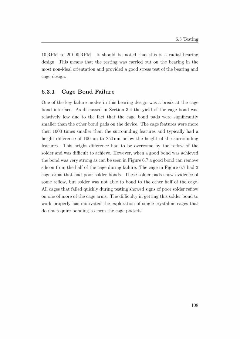
6.3 Testing
10 RPM to 20 000 RPM. It should be noted that this is a radial bearing
design. This means that the testing was carried out on the bearing in the
most non-ideal orientation and provided a good stress test of the bearing and
cage design.
6.3.1 Cage Bond Failure
One of the key failure modes in this bearing design was a break at the cage
bond interface. As discussed in Section 3.4 the yield of the cage bond was
relatively low due to the fact that the cage bond pads were significantly
smaller than the other bond pads on the device. The cage features were more
then 1000 times smaller than the surrounding features and typically had a
height difference of 100 nm to 250 nm below the height of the surrounding
features. This height difference had to be overcome by the reflow of the
solder and was difficult to achieve. However, when a good bond was achieved
the bond was very strong as can be seen in Figure 6.7 a good bond can remove
silicon from the half of the cage during failure. The cage in Figure 6.7 had 3
cage arms that had poor solder bonds. These solder pads show evidence of
some reflow, but solder was not able to bond to the other half of the cage.
All cages that failed quickly during testing showed signs of poor solder reflow
on one of more of the cage arms. The difficulty in getting this solder bond to
work properly has motivated the exploration of single crystaline cages that
do not require bonding to form the cage pockets.
108

6.3 Testing
Figure 6.7: SEM image of a cage that quickly during testing. The
6.3.2 Tribometer Results
Tribometer testing was carried out on the bearings for low and high speeds.
The measurements were used to test the validity of the model presented in
Section 4.7. Though the characteristic curve of the model is similar to the
measured values the predicted values were lower than the measured torque.
The model was modified in two stages. First the low speed measurements
were used to assess the value ofMl as the centrifugal forces would be negligible
at the lower speed. Then, with the modified calculation for Ml the model
was compared to the high speed results to assess the effects of the centrifugal
force. The results of these analysis steps are described below.
2 devices were measured at speed of 50 RPM to 550 RPM in increments
of 50 RPM. The results of this testing is presented in Figure 6.8 with a
plot of a modified model (Equation 6.1) for the torque. Measurement of
the torque is less stable at lower speeds, therefore the spread of the torque
measurements is shown on the graph as error bars. It should also be noted
the torque is negative because the balls are sliding at lower speed rather than
rolling, therefore the outer ring is moving in the direction of the motor which
is represented as a negative value. It was found that the torque on the outer
109
6.3 Testing
platform predicted by Equation 4.19 was 3 orders of magnitude lower than
the values measured during testing. As was stated in Section 4.7 the value of
z and y used to calculate fl are determined empirically for existing macro-
scale bearing. It was determined by analyzing the measured torque that the
value of z is not appropriate for this bearing design. If we substitute z = 0.8
instead of the value of z = 0.008 reported in [Harris 06b] the model closely
fits the measured torque values for the low speed measurements. Centrifugal
forces are negligible at these lower speeds so the frictional toque is nearly
constant as would be expected from the model.
Figure 6.8: The measured torque of the bearing at low speeds and the pre-dicted torque from Equation 6.1. The error bars indicate the range of themeasurement for each speed and the connected points are the average of themeasurements.
After modifying the model for to predict a more realistic value for Ml the
model was compared the the high speed measurements. To obtain the high
speed torque measurements, a bearing was tested at speeds of 1000 RPM to
20 000 RPM in increments of 200 RPM. An average of three tests is plotted
in Figure ?? with the predicted toque values of the modified model(Equation
110

6.3 Testing
6.1.) The crossing at the x-axis does not represent that no torque was mea-
sured at the outer platform. In the range from approximately 6000 RPM to
8000 RPM the balls are transitioning from sliding to rolling and there is a
mixture of both which results in reducing the measured displacement of the
outer platform. It was found that the measured centrifugal torque was 3
times greater than the value predicted by Equation 4.19.
These observations led to the following modified model for the total fric-
tional torque for the bearings presented in this chapter:
M = 3× (2.19× 10−8)NbdmD3n2
m
do2 − 0.8
((FaCs
)0.33)Fadm (6.1)
Figure 6.9: The average of the measured torque for the bearing over 3 testruns at speeds of 1000 RPM to 20 000 RPM with the predicted torque fromEquation 6.1.
The measured results and the modified model indicate that the friction
torque at higher speeds does change proportional to ω2; which indicates that
the centrifugal torque does play a significant in the bearing loss at higher
111

6.3 Testing
speeds as predicted. The significant difference between the original model
of the load torque and the measured load torque can likely be attributed
to both geometric and scaling factors. Figure 6.10 shows the measured and
predicted power loss which is proportional to ω3 as expected.
Figure 6.10: The graph shows the measured power loss in the bearing from1000 RPM to 20 000 RPM. At 1000 RPM the bearing loss is approximately0.5 mW. As the speed increases and the centrifugal force plays a more dom-inate role and increases the bearing loss.
6.3.3 Wear
After 5 hours of testing the second tested device was soaked in chrome etchant
to break the solder bonds. The parts of the bearing were then viewed in the
SEM to evaluate any indication of wear. Minimal wear was noted on bearing
interfaces. There was some indication of abrasive or shock wear in the ball
pockets of the cage as seen in Figure 6.11. The edge of the ball contact with
stator and the rotor both showed signs of abrasive wear in the form rounding
of the interface. Figure 6.12 shows the wear on the rotor and also indicates
the location of over-etching damage on the rotor. Figure 6.13 shows wear
damage at the ball contact on the bottom half of the stator.
112

6.3 Testing
Figure 6.11: SEM image of the cage after testing. The circles indicate thelocations of the wear on the ball pockets. The damage to the cage arms isdue to wear as similar damage is not seen in Figure 6.7 on a cage that failedafter very little testing
Figure 6.12: SEM image of the top of the silicon rotor after testing. Fab-rication damage is indicated in the boxes and wear damage is contained inthe ellipse. The wear damage appears as a rounding at the edge of the rotorwhere the rotor and ball contact each other. This damage is not seen inuntested devices.
113

6.4 Discussion and Conclusions
Figure 6.13: SEM Image showing the wear on the bottom half of the stator.Wear damage is contained in the ellipse. The wear is a rounding of the statoredge where the stator and the ball contact each other. This rounding is notpresent in untested device.
6.4 Discussion and Conclusions
As a first proof of concept this bearing design provided an excellent test case
for designing and fabricating ball bearings with an integrated ball cage. The
solder bond at the center of the cage was the only point of failure in the
device and this may have been due to the design of the solder pads and the
bonding process. The fabrication process also caused damage to the raceway
of the bearing, leading us to explore solutions to this damage when designing
new devices. Overall, this design proved that the silicon cage could survive
for several hours of continuous operation at speeds of up to 20 000 RPM with
a thrust load of 60 mN. This design also showed a measurable difference
when the balls were in the sliding and rolling regimes. Further the model for
the friction torque presented in Section 4.7 was found to under estimate the
frictional torque measured for these bearings. The model for the load torque
predicted values 3 orders of magnitude below the measured values. This
difference could be attributed to geometric and scaling differences between
these bearings and the bearing that we used to create model. The centrifugal
114

6.4 Discussion and Conclusions
torque was also under estimated but only be a factor of 3. The model has
been modified to reflect these observations. The results do indicate that
the frictional torque does increase proportional to ω2 which indicates that
centrifugal force does play a significant role in the bearing loss at higher
speeds.
115

Chapter 7
In-Situ Fabrication of a
Monolithic Silicon Ball Cage
The dual row style cage was designed to demonstrate the fabrication of a
retainer ring from a single piece of silicon. Due to the fact that the weak-
est point in the radial design presented in Chapter 6 was the solder bond
in the ball cage, a geometry and fabrication process that would allow for
creating a cage without the need for bonding together parts of the cage were
explored. The focus of this exploration was to create a process that would al-
low for creating the desired geometry while keeping the silicon cage attached
to the stator and rotor until after the device was assembled. This work was
presented in [Hergert 13a].
The fabrication process consists of a novel method of using windows in the
top and bottom wafers of the device to etch away sacrificial beams located
on the center wafer that holds the cage and rotor in place, this is shown
in Figure 7.1. This process could be adapted for any multi-wafer process in
which the design requires that a part on one wafer be released after the wafer
stack is assembled. Examples would be complex mechanics such as a watch
assembly, the parts of power harvesters or, as in this case, a rotary device.
A conceptual drawing of the bearing design can be found in Figure 7.2.
116

Figure 7.1: Conceptual drawing of the multi-wafer release etch technique(left), DRIE is used to etch a sacrificial beam through windows that havebeen etched in the upper and lower wafers of the 3 wafer stack. A CADdrawing of the bearing design with red arrows to indicate the location of thesacrificial beams and the rotor release channel before release etching (rightA) and after release etching (right B.)
Figure 7.2: Conceptual drawing of the dual groove style bearing design. Thecutaway (lower right) shows the orientation of the parts of the device undera thrust normal load.
117

7.1 Design
7.1 Design
Several fabrication methods provide the possibility of creating a cage design
from a single piece of material. Several initial ideas came from [Jaeger 02].
One option is to create structures by building the device on the surface of
a bulk silicon substrate, then use an isotropic etching process for release as
described in [Kovacs 98] or [Fedder 96]. However, this method would have
presented design challenges and might have suffered from poor geometry
control during the isotropic release process. Another option for creating the
device would have been to create the cage on the surface of a silicon substrate
with an intermediate sacrificial layer. This method has been shown to work
for devices made of polysilicon using silicon dioxide as the sacrificial layer as
in [Mehregany 98] or [Pister 92]. After etching away the silicon dioxide layers
the structures are free to move. This is a very attractive option, however,
we were not able to create the polysilicon layers needed for this technique in
our laboratory. Also, it would not have been possible to use this method to
create a cage over or within the deep trench of the bearing raceway. Another
option would have been to create the entire bearing by defining the geometry
in layers of electroplated metals formed in or on a polymer sacrificial layer
as shown in [Guckel 98] and [Cohen 10]. This would have required multiple
masks and it would have been challenging to incorporate the balls into the
bearing design.
In [Frechette 05] a sacrificial silicon beam was used to hold a turbine in
place during the fabrication process, and this tab was snapped out using
micromachined silicon needles before testing. A further improvement is the
use of a laser to remove the sacrificial tabs as described in [Lin 99]. A similar
method is described in [Abraham 08].Using a silicon beam to support the ball
cage during device assembly seemed to be the most accessible design option
with the processing techniques available. This method allows for creating
the exact geometries needed for the device, uses standard DRIE processing
to create the structures, and provides a rigid and reliable support mechanism
to hold the cage in place during assembly. However, a method of removing
the support beams was required. As a DRIE step is required to release the
118

7.1 Design
rotor of the bearing after assembly, it seemed natural to try to use this etch
step to remove the sacrificial beams as well. This idea was further supported
by the use of stencils as masks as reported in [Pang 88] and [Villanueva 09].
The beam release concept is illustrated in Figure 7.3.
Figure 7.3: Conceptual drawing of the cage support release etching. This isdone in two DRIE etch steps, one from the top and one from the bottom.
The design of the bearing required that windows were etched all the
way through the silicon of the top and bottom of the device to expose the
silicon beams holding the cage in place on the middle wafer of the device.
These windows had to be large enough to compensate for etch lag effects
which are dependent on feature size and that become more dominant with
increased feature depth. Etch lag is further explained in Section 3.2.4. The
etch windows with and sacrificial beam can seen in Figure 7.4.
In our first investigation of the sacrificial beam release method we ex-
plored using 8 beams to secure the cage and the rotor. These beams were
located above the balls and therefore only exposed to DRIE etching for one
of the rotor release etch steps. The beam had a width of 20 µm and the etch
window had a height(in the radial direction) of 40 µm and a width of 80 µm.
119

7.1 Design
The perceived advantages of this design was that the beams were closer to
the surface of the middle wafer and thus closer to the top of the etch window,
8 beams provided excellent support during assembly, and the beam was pro-
tected during one of the DRIE etching cycles by the ball which was intended
to eliminate excessive etch damage to the bearing side wall. However, This
design did not allow sufficient time for the beam to be etched all the way
through on a single etch cycle; only 50 µm of the total 150 µm beam thickness
was etched.
The final design had only 4 beams which were exposed to DRIE etching
during both the top and bottom rotor release etch cycles. This was accom-
plished by designing the beams into the space between the top and bottom
ball in the cage. The cage release windows were also increased in size to
a height of 110 µm and width of 80 µm. The thickness of the cage support
beams was kept at 20 µm. With these design changes the cage support beams
were completely etched away during the rotor release etch steps. A diagram
showing the window design with the beam is provided in 7.4 and a compar-
ison of the two design iterations is provided in Table 7.1. The final layout
design of the device top, raceway and middle are shown in Figure 7.5.
120

7.1 Design
Figure 7.4: Drawing of the cage release window showing the cage supportbeam, the top and bottom balls, the release channel and measurement labelsfor the cage features.
Parameter First Design Final DesignBeam Width (Wb) 20 µm 20 µmWindow Width (Ww) 40 µm 150 µmWindow Height (Hw) 80 µm 110 µmBeam Thickness 125 µm 100 µmTotal Support Beams 8 4Release Etch Beam Exposure Top Only Top and BottomSuccessful Release Etch No Yes
Table 7.1: Design parameters for the cage support beam and etch windowsfor the first and second design iterations.
121

7.1 Design
Figure 7.5: Layouts on both sides of the top/bottom wafers, and on thecenter wafer of the dual row style design with labels indicating importantfeatures.
122

7.2 Device Fabrication
7.2 Device Fabrication
Due to the complexity of the device fabrication, the process has been broken
up into 3 distinct sections: Top and Bottom Die Fabrication, Center Die Fab-
rication, and Device Assembly and Release Etching. For more information
on the processes described in this section please refer to Chapter 3.
7.2.1 Top and Bottom Die Fabrication
The top and the bottom die are fabricated on the same wafer using a100 mm
diameter, p-type, <100>, DSP silicon wafer with a thickness of 525±25 µm.
The wafers also had 1 µm of thermally grown silicon dioxide. A descrip-
tion of each processing step follows. The steps are labeled with the letter
corresponding to the depiction of the step in Figure 7.6.
123

7.2 Device Fabrication
Figure 7.6: Device fabrication process flow for the top and bottom die usedin the dual row style cage device.
7.2.1.1 Step A (Front Side)- Plate Solder Pads
The wafer is sputter coated with a chrome and copper seed layer (not shown
in the process flow diagram.) The wafers are coated with photoresist and
patterned with the solder pad mask. The solder pads are electroplated with a
2 µm nickel diffusion barrier, 3 µm of tin and 300 nm of gold. The photoresist
is then stripped and the exposed seed layer (not shown in the diagram) is
etched to expose the silicon dioxide below.
124

7.2 Device Fabrication
7.2.1.2 Step B (Front Side) - Pattern Raceway Stand-off Trench
The wafer is coated with photo resist and is patterned with the raceway
stand-off mask. The exposed oxide is then etched using RIE. The photoresist
is then stripped from the wafer.
This feature will be etched below the level of the contact region of the
ball bearing raceway. This allows for etching the cage release window all
the through the wafer. Initial designs that did not have this recess showed
damage to the contact region of raceway caused during the release etch steps.
Devices with the recessed showed less damage to the raceway from the win-
dow and release etch.
7.2.1.3 Step C (Front Side) - Pattern the Raceway and Etch the
Raceway Stand-Off
The wafer is coated with photoresist and the raceway is patterned on the
wafer. The raceway stand off (patterned in the oxide in the previous step) is
etched to a depth of 100 µm using DRIE. As the raceway is protected by oxide
it is not etched. The photoresist is left on the wafer for the next processing
step.
7.2.1.4 Step D (Front Side) - Etch Bearing Raceway
The exposed oxide is etched from the the wafer. The raceway is etched to a
depth of approximately 225 µm using DRIE. The depth of the standoff also
increased during this etch creating a stepped profile. After the raceway is
etched, the photoresist is removed from the wafer. This completes all of the
processing on the top side of the wafer.
7.2.1.5 Step E (Back Side) - Define Cage Release Window and
Identification Marks
The back side of the wafer is coated with photoresist and the cage release
windows are patterned in the oxide using RIE. The die identifier and the
125

7.2 Device Fabrication
device release lines are also etched in the oxide. After the oxide etch the
photoresist is stripped from the wafer.
7.2.1.6 Step F (Back Side) - Define Testing Adaptor Feature and
Bearing Release Channels; Pre-Etch Cage Release Win-
dow
Photoresist is coated on the wafer. The bearing release channel and the test
adaptor feature are patterned in the resist. The cage release windows are
etched to a depth of approximately 150 µm. The photoresist is left on the
wafer after this step.
7.2.1.7 Step G (Back Side) - Pre-Etch Testing Adaptor Feature
and Bearing Release Channels; Etch Cage Release Win-
dow Through the Wafer
The exposed oxide is etched by RIE using the photoresist from the previous
step as a mask. The test adaptor feature and the bearing release channel
are etched to a depth of approximately 125 µm using DRIE. During this etch
the cage release windows and the device edge are etched through the wafer
(meeting the features etched on the front side of the wafer.) This leaves the
windows needed to etch the beams holding the cage in place on the center
die of the device.
7.2.1.8 Images of Fabricated Top and Bottom Die
Below are SEM images of completed top and bottom die used in the fabrica-
tion of the dual row style cage bearing. The devices depicted in the images
were early prototypes and show signs of spires and the loss of solder pads (in
Figure 7.7.) These sample images do show the die with the features and etch
depths used in the final device.
126

7.2 Device Fabrication
Figure 7.7: SEM image of the raceway of the bottom die for the dual rowstyle cage device.
Figure 7.8: SEM of the raceway side of the bottom die for the dual row stylecage device, the arrows indicate features that have been etched completelythrough the wafer.
127

7.2 Device Fabrication
Figure 7.9: SEM image of the top of the top die for the dual row style cagedevice. The device identification marks, test adaptor features, bearing releasechannels and the cage release windows are clearly visible.
7.2.2 Center Die Fabrication
The center die is fabricated using a 100 mm diameter, p-type, <100>, DSP
silicon wafer with a thickness of 525±25 µm. The wafer also had 1 µm of
thermally grown silicon dioxide. A description of each processing step follows.
The steps are labeled with the letter corresponding to the depiction of the
step in Figure 7.10.
The fabrication process flips from the top side to the back side and then
back to the top side of the wafer. This is due to the fact that the wafer would
often break during the second electroplating process if the top side had deep
etched features. In order to eliminate the risk of breaking the wafers during
the second plating process all of the DRIE etching was done after both sides
of the wafer had been electroplated with the solder pads.
128

7.2 Device Fabrication
Figure 7.10: Device fabrication process flow for the center die used in thedual row style cage device.
7.2.2.1 Step A (Top Side) - Plate Solder Pads
The wafer is sputter coated with a chrome and copper seed layer (not shown
in the process flow diagram.) The wafers are coated with photoresist and
patterned with the solder pad mask. The solder pads are electroplated with a
2 µm nickel diffusion barrier, 3 µm of tin and 300 nm of gold. The photoresist
is then stripped and the exposed seed layer (not shown in the diagram) is
etched to expose the silicon dioxide below.
129

7.2 Device Fabrication
7.2.2.2 Step B (Top Side) - Define Cage with Support Beams
Photoresist is deposited on the top side of the wafer. The cage with sup-
port beams is patterned in the photoresist and then RIE is used to etch the
exposed silicon dioxide. The photoresist is then stripped from the wafer.
7.2.2.3 Step C (Back Side) - Plate Solder Pads
The top side of the wafer is coated with photoreist to protect the existing
solder pads during the electroplating step. The back side of the wafer is then
sputter coated with a chrome and copper seed layer (not shown in the process
flow diagram.) The wafers are coated with photoresist and patterned with
the solder pad mask. The solder pads are electroplated with a 2 µm nickel
diffusion barrier, 3 µm of tin and 300 nm of gold. The photoresist is then
stripped and the exposed seed layer (not shown in the diagram) is etched to
expose the silicon dioxide below.
7.2.2.4 Step D (Back Side) - Define Cage with Support Beams
Photoresist is deposited on the back side of the wafer. The cage with sup-
port beams is patterned in the photoresist and then RIE is used to etch the
exposed silicon dioxide. The photoresist is then stripped from the wafer.
7.2.2.5 Step E (Back Side) - Pattern Cage Without Support Beams
and Pre-Etch Cage With Support Beams
Photoresist is deposited on the wafer and is patterned with the cage design
without support beams. The pattern from the previous step is the etched to
a depth of approximately 50 µm. This etch will establish the height of the
beams that will support the rotor and the cage during the assembly of the
device. The photoresist is left on the wafer for the next step.
130

7.2 Device Fabrication
7.2.2.6 Step F (Back Side) - Etch Cage to Final Depth and Reduce
Beam Thickness
The exposed silicon dioxide is etched. This will expose the silicon at the top
of the support beams. The cage and the beams are etched approximately
225 µm so that the ball pocket is at a final depth of 275 µm. This also brings
the area around the cage to a depth below the center of the wafer thickness.
The photoresist is stripped from the wafer and this completes the processing
of the back side of the wafer.
7.2.2.7 Step G (Top Side) - Pattern Cage Without Support Beams
and Pre-Etch Cage With Support Beams
Photoresist is deposited on the top side of the wafer. The photoresist is
patterned with the cage design without the supporting beams. In Step B
(Section 7.2.2.2) the cage with support beams was patterned on the top side
of the wafer, therefore the oxide pattern that defines the support beams
already exists on this side of the wafer. This pattern is etched to a depth
of approximately 50 µm. This established the height of the beam that will
support the rotor and the cage during device assembly. The photoresist is
left on the wafer for the next step.
7.2.2.8 Step H (Top Side) Etch Area Around Cage Through the
Wafer and Reduce the Beam Thickness
The exposed silicon dioxide is etched from the wafer, thus exposing the silicon
on top of the support beams. DRIE is then used to etch the cage and the
beams to a depth of 225 µm. This provides a final ball pocket depth of
275 µm and support beam thickness (total from both sides of the wafer) of
approximately 100 µm. The regions between cage and the rotor and the stator
are etched completely through the wafer. Thus the rotor and the stator are
held in place by only the 4 support beams. The photoresist is stripped from
the wafer and the wafer is broken into die for assembly.
131

7.2 Device Fabrication
7.2.2.9 Images of Fabricated Center Die
Below are SEM images of the center die made by following the process flow
described above. From the top view, presented in Figure 7.11, it is possible
to see the regions that have been etched through the wafer around the edges
of the cage. The image also shows how the 4 beams that support the cage
and the rotor by attaching them to the stator. The Angled view of the device
clearly shows the varying step heights that have been achieved in the process
flow. The reduced height of the support beams is also evident in the image.
Figure 7.11: SEM image of the center die used for the dual row style cagedevice. The cage can be seen at the center of the device supported by 4beams. The black regions in the image have been etched through the wafer.
132

7.2 Device Fabrication
Figure 7.12: SEM image of the center die used in the dual row style cagedevice. The angle of the device in the image shows the difference in theheight between the top of the wafer, the ball pockets and the tops of thebeams. The black regions have been etched through the wafer.
7.2.3 Device Assembly and Release Etching
After the top, bottom and center die are made the device must be assembled
and the cage and the rotor must be released. The following sections will
detail the steps that are required for the assembly and release. The steps are
labeled with the letter corresponding to the depiction of the step in Figure
7.13.
133

7.2 Device Fabrication
Figure 7.13: Device fabrication process flow for assembly and release etchingof the dual row style cage device. The red arrows show the location of thesacrificial beams and the bearing release channel before (A) and after (B)the release etches.
7.2.3.1 Step A - Device Assembly
The device is assembled by first placing steel balls in the ball pockets on
one side of a center die. Solder flux is then painted onto the solder pads and
134

7.2 Device Fabrication
200 µm diameter solder balls are placed at the center of each pad. Steel align-
ment pins are inserted into the alignment holes located on either side of the
die. The bottom die is then slid onto the alignment pins. The center/bottom
die stack is then flipped over while pressing the stack together with tweezers.
The alignment pins keep the stack, steel balls and solder balls in the proper
position. Steel balls are then inserted into the ball pockets on the other side
of the center die. The top die is then slid onto the alignment pins, completing
the 3 wafer stack. The die stack is then transferred to a custom bond aligner
where a low force is applied to the stack. A butane torch is used to rapidly
head the stack and reflow the solder balls. During the heating process the
steel alignment pins expand and creating a snug fit with the alignment holes
thereby improving the overall alignment of the stack during solder reflow.
After reflow the devices are ready for the final release etching.
7.2.3.2 Step B - Release Etching
After assembly the devices are mounted on a backing wafer with the bottom
side facing up. The patterned silicon dioxide from the previous processing
steps is used as a mask for the final release etch steps. The bottom side of
the device is etched, using DRIE, until the bearing release channel reaches
the bearing raceway. During this etch the support beams, holding the cage
and rotor in place, are also etched part of the way through. This is due to
the windows in the silicon located above the beams.
After the bottom of the device is etched the device is removed from the
backing wafer and mounted on a new backing wafer with the top of the device
facing up. The top bearing release channel is then etched, using DRIE, until
it meets the raceway. The support beams are completely etched away during
this step. Thus at the completion of this step, when the device is removed
from the carrier wafer, the rotor and cage are completely released from the
stator.
135

7.2 Device Fabrication
7.2.3.3 Images of Assembled and Released Devices
Figures 7.13 and 7.14 show SEM images of the top and bottom of assembled
and released devices. The top view presented here is of a 6 ball design that
was too unstable survive testing. The diameters of the top and bottom release
channels differ because these are thrust bearing designs and therefore have a
load support surface on the rotor at the top of the device and on the stator
at the bottom of the device. An image of the released cage can be found in
Figure 7.18 and a released rotor can be seen in Figure 7.19. The supports
beams are completely etched from the cage and the rotor with only a slight
feature to indicate where the beams were located before etching.
Figure 7.14: SEM image of the top of an assembled and released dual rowstyle cage device. The test adaptor, bearing release channel, cage releasewindows and identification marks are visible.
136

7.3 Testing
Figure 7.15: SEM image of the bottom of an assembled and released dualrow style cage device. The bearing release channel, cage release windows andthe identification marks are visible.
7.3 Testing
The devices were tested on the micro-tribometer discussed in Section 5.1. A
thrust load was applied to the rotor (center) of the bearing. One device that
contained 8 balls was tested successfully. Another device that contained only
6 balls was extremely unstable and failed catastrophically during testing,
breaking the device and the silicon test platform.
The 8-ball device that was successfully tested had a cage width of 300 µm,
a diameteral play (Pd) of 40 µm. The raceway diameter (dm) was 1.75 mm. A
thrust load of 40 mN was applied to the bearing. It was test at speed ranging
from 50 RPM to 5100 RPM.
7.4 Test Results
The measured torque of the dual row device is plotted in Figure 7.16. In this
figure the torque is plotted as a function of the speed. As can be seen in
the figure, the bearing did not show signs of ball sliding at any of the mea-
sured speeds. The measured frictional torque does not show the expected
137

7.4 Test Results
relationship to centrifugal forces, as was observed and described in Section
6.3.2, there is also no indication of ball sliding at any of the measured speeds.
The frictional torque is almost constant over the tested speed range, with the
exception of a jump in the measured torque above 4000 RPM. The torque
is also significantly higher than seen in the radial design. For example the
frictional torque for this design at speeds below 4000 RPM is close to mea-
sured the fictional torque of the radial bearing at 18 000 RPM. The observed
frictional torque implies that this design is much less efficient than the radial
design. The power loss of the bearing is plotted in Figure 7.17. Even though
the power loss varies with ω rather then ω2, as seen in the radial design, the
power loss over the measured range is almost and order of magnitude greater
for the dual row bearing.
Figure 7.16: Torque measurements of 4 tests of the dual row ball bearingdesign.
138

7.5 Wear
Figure 7.17: Measured bearing loss of the dual row ball bearing design forall 4 tests plotted with the power loss for the radial bearing over the samerange. Though the power loss varies with ω rather than ω2, as seen in theradial design, the loss of the dual row bearing is almost an order of magnitudegreater than the radial design over the same range.
7.5 Wear
Though minimal wear was apparent on the bearing it should also be noted
that the bearing was only tested for a total of 2 h. Abrasive wear is apparent
at the top edges of the cage pockets. This wear is similar to seen at the edge
of the cage pockets in the radial bearing design and due to abrasion from the
ball and possible from ball/cage shock. The cage wear is shown in Figure
7.18. The ball contact surfaces on both the rotor and stator showed signs of
abrasive and possible adhesive wear. The pattern on both raceway surfaces
was consistent with that seen on the contacts of other thrust style bearings.
Figure 7.19 shows the wear on the rotor raceway, while Figure 7.20 shows
the wear on the stator raceway.
139

7.5 Wear
Figure 7.18: SEM image of the cage after testing. Wear at the edge of theball pocket is indicated in the ellipse on the left. The location of the supportbeam is indicated in the ellipse on the right; there is very little indication ofthe location of the support beam after the release etch.
Figure 7.19: SEM image of the rotor after testing. The arrow on the leftpoints to rotor wear which appears as a discolored region on raceway. Theellipse in the figure indicates where the support beam was located beforeetching.
140

7.6 Discussion and Conclusions
Figure 7.20: SEM image the stator after testing. The arrow indicates thelocation of the wear, which appears as a discolored region on the raceway.Pillar defects are present at the edge of the raceway and are an artifact ofthe multi-step etching processes.
7.6 Discussion and Conclusions
This chapter presented a new fabrication technique that allows for the release
of moving parts that are embedded in the middle of a multi-wafer stack.
This is possible by using DRIE to etch windows through the top and bottom
wafers and then have beams on the center wafer that are exposed to DRIE
etching after assembly. The technique was applied to a ball bearing with
a dual row style cage. Though the cage design is inefficient and unstable
the fabrication technique has proven to be viable. In Figures 7.18 and 7.19
the regions where the cage support beams were located are visible. The
beams are completely removed from the cage and rotor surfaces with only
small features remaining to indicate where the beams were attached. It
should also be noted that in Figure 7.19 the etch windows are visible and
that the windows and the surrounding features have experienced minimal
damage during the release etch process. This is a new release technique that
could have broad application in the fabrication of gear trains, power MEMS
devices, or any application in which a part with a large range of motion must
141

7.6 Discussion and Conclusions
be released after assembly of a device.
Though the fabrication technique proved to be a valid design approach, tt
should be noted that the design of the ball cage is this chapter is significantly
less efficient than the radial design presented in Chapter 6. The tests results
show an almost constant frictional torque over the tested range of 50 RPM
to 5000 RPM. And though the power loss of this design is proportional to
ω, rather than ω2 as seen in the radial design, the power loss for this design
is almost an order of magnitude greater. Due to the inefficiency of and the
complexity of this design further exploration of this cage geometry is not
recommended. However, the fabrication technique could have much broader
application in complex MEMS devices.
142

Chapter 8
Micro-Turbines with Integrated
Silicon Ball Cage
This chapter describes the investigation of the effect of incorporating silicon
retainers into silicon MEMS thrust micro-ball bearings reported in [Waits 10]
and integrated in the SMT devices described in Section 5.2. Section 4.1 de-
scribes some of the inherent advantages of using a ball cage in ball bearing
designs. The bearing investigated in this chapter is a thrust-style bearing
which lends itself to incorporation of a monolithically fabricated silicon re-
tainer. To allow functional testing the bearing is integrated with a silicon
micro-turbine (SMT), following [McCarthy 09]. This platform was chosen
as it provides a proven method for actuation of the bearing during charac-
terisation. Several different retainer designs were investigated in turbines
of two sizes, with 5 mm- and 10 mm-diameter turbine rotors respectively.
Photographs of devices of both sizes, together with a cut-away schematic
view showing the retainer, are shown in Figure 8.1. The different designs
were compared in terms of losses, inferred from the variation of turbine in-
put power with rotation speed; measurements of repeatability and longevity
were also made on selected devices.
An early investigation of the retainer geometries in 5 mm-diameter SMTs
was reported in [Hergert 11]. Since the publication of the early work, the
fabrication process for the devices was improved to allow for successfully
143

8.1 Retainer Ring Design Considerations
fabricating and test devices with a 10 mm rotor diameter, this work was first
repoted in [Hergert 13b]. This was achieved by making the turbine with
a 1 mm-thick silicon wafer rather than a 500 µm thick wafer and changing
the etching steps to better account for etch lag. These changes allowed for
an increase in the thickness of silicon above the bearing raceway, making it
sufficient to withstand the forces of bearing operation in larger devices.
Figure 8.1: Photographs of the both the 5 mm and 10 mm devices with aBritish Pound coin for scale (top), and a cutaway view of the device showingthe retainer ring (bottom).
8.1 Retainer Ring Design Considerations
Figure 8.2 shows a cut-away schematic view of a conventional thrust bearing
incorporating a so-called ball-riding (BR) retainer [Harris 06b]. In this style
of bearing, the retainer is supported entirely by the rolling elements which
are held captive in suitably shaped pockets, and consequently there is no
contact between the retainer and the bearing rings. Alternative designs for
radial/mixed load bearings employ inner ring (IRL) or outer ring (ORL) land
riding retainers which are sized to fit the cylindrical surface of either the inner
or outer bearing ring [Harris 73]. IRL retainers are driven by a friction force
between the retainer and the inner ring, and under optimal conditions this
144
8.1 Retainer Ring Design Considerations
can result in negligible loading of the rolling elements by the retainer. ORL
retainers are guided by the outer ring and are therefore subject to a drag
force; this type of retainer tends to be used in high-speed applications.
Figure 8.2: Cut-away schematic view of a conventional thrust bearing witha ball-riding retainer.
Five different designs of retainer ring were investigated for the work pre-
sented in this chapter, designated as Full Ring, Full Skeleton, Half Skeleton,
Outer Open and Inner Open. Scanning electron microscope (SEM) images
of all five retainer types are shown in Figure 8.3. Also shown in this figure
are schematic cross-sections for the different retainer types. The left-hand
schematic also illustrates how the bearing and micro-turbine are integrated;
the device is assembled at die level as a bonded two-die stack, comprising a
lower ”thrust” die and an upper ”turbine” die, with the steel balls and cages
manually inserted between the die. The bearing is formed at the interface
between the two dies, with the rotor blades and guide vanes of the turbine
being defined in the upper surface of the turbine die.
145

8.1 Retainer Ring Design Considerations
Figure 8.3: (a) SEM images showing the 5 mm retainer ring designs: FullRing (top left); Full Skeleton (top right); Half Skeleton (bottom left); OuterOpen (bottom right); Inner Open (centre). (b) Schematic cross-sections ofbearings with the different retainer types.
Comparing Figures 8.2 and 8.3, two important differences, both arising
from micro-fabrication process constraints, can be seen between the MEMS
thrust bearing and its conventional counterpart. Firstly, the raceways on
the conventional bearing are curved in cross-section so that the balls have
a single point of contact with each raceway and the bearing is inherently
self-aligning when subject to an axial load. In contrast, the silicon raceways
are rectangular, with the balls riding on essentially flat surfaces top and
bottom. The balls are constrained to follow a nominally circular path by the
146

8.1 Retainer Ring Design Considerations
sidewalls of the bearing raceway, with which they make intermittent contact,
and also by the retainer. Secondly, while the pockets in the conventional
retainer are shaped to enable it to ride on the balls, this cannot be achieved
with the silicon retainer because the pockets are cylindrical. Instead the
Inner Open retainer rides on the land adjacent to the bearing raceway on the
outer (stator) side, while the Outer Open retainer is supported by the land
on the inner (rotor) side. The inner land is slightly elevated with respect
to the outer, and consequently the Full and Skeleton retainers should ride
in the same way as the Outer Open type. However, if the height difference
is sufficiently small then bearing vibration and dynamic distortions of the
retainer may bring it into contact also with the outer land. The different
silicon retainers can reasonably be classified as either inner ring or outer ring
land riding, though they differ from conventional IRL and ORL retainers in
that they ride on flat surfaces in the plane of the bearing rather than on
cylindrical surfaces. It should also be noted that interactions between the
retainer and the balls when the bearing is operational may cause the retainer
to ride up and make contact with the top of the retainer raceway; the top
of the raceway is recessed to provide a stand-off and reduce the contact area
under these conditions. Key design parameters for the bearings developed in
this work are given in Table 8.1.
The width of the bearing raceway was set at 510 µm giving a clearance
of 5 µm either side of the 500 µm-diameter steel balls. This clearance deter-
mines the lateral play in the rotor position, and the value chosen was the
smallest that would guarantee easy insertion of the balls, taking into account
fabrication tolerances. The width of the retainer raceway was chosen to give
a clearance of 25 µm either side of a Full Ring retainer, ensuring that no
retainer-raceway sidewall contact would occur with any of the designs. The
bearing raceway was made slightly higher than the ball radius to ensure a
planar contact between the ball and the raceway sidewall. The height of the
retainer raceway was then set so that the combined height of the raceways,
including the thickness of the solder bond between the wafers and the recess
in the top of the retainer raceway, was nominally 10 µm larger than the ball
diameter i.e.
147

8.1 Retainer Ring Design Considerations
Parameter Description Large SmallDevice Device
RBP Radius of ball path 5000 2600RI Retainer inner radius - full, outer open 4647.5 2247.5
- inner open 4787.5 2387.5RO Retainer outer radius - full, inner open 5352.5 2387.5
- outer open 5212.5 2812.5g Ball pocket opening - outer open 278 284
- inner open 267 261RB Ball radius 250RP Pocket radius in retainer 252.5WBR Width of bearing raceway 510WRR Width of retainer raceway 755HBR Height of bearing raceway 260HRR Height of retainer raceway (incl. solder) 245HSO Stand-off height 5HR Height of retainer 225
Table 8.1: Key design parameters for large (10 mm) and small (5 mm) devices.All dimensions are in µm.
148

8.2 Retainer Ring Design Variations
Cage Name No. Balls Ball Fill Contact Stability Mechanical10 mm/5 mm Factor Area Strength
Full Ring 32 / 16 50% High High HighFull Skeleton 32 / 16 50% Medium High MediumHalf Skeleton 16 / 8 25% Very Low Low MediumOuter Open 32 / 16 50% Low Medium LowInner Open 32 / 16 50% Low Medium Low
Table 8.2: Comparison of retainer parameters by geometry.
∆ = HBR +HRR +HSO − 2RB = 10 µm (8.1)
where all the variables are as defined in Table 8.1. In choosing the design
value of ∆, tolerances in etch depth and solder bond thickness were taken
into account. It is essential that ∆ > 0 so that there is clearance above the
balls while the device is being assembled.
8.2 Retainer Ring Design Variations
The five retainer designs were chosen to explore the effects on the bearing
performance of sliding friction, retainer rigidity, ball pocket shape and ball
complement. The differences between the designs are summarised in Table
8.2. Considering first sliding friction, this is expected to be most significant
in the Full Ring design which has the largest overlap area with the inner
and outer lands. The Skeleton designs reduce the overlap area on either
side by removing material between the ball pockets, while the Open designs
eliminate it entirely on one side of the raceway. Removal of material from
the Skeleton and Open designs will also reduce the mechanical rigidity of the
retainer. This has been found to improve the performance in conventional
bearings under some loading conditions [Weinzapfel 09].
In addition to distributing the balls uniformly around the raceway, the
retainer will also limit the radial excursions of the balls, encouraging them
to follow a stable circular trajectory and reducing the extent to which they
interact with the raceway sidewalls; this is expected to be beneficial in terms
149

8.2 Retainer Ring Design Variations
of friction and wear. The radial play allowed by the ball pockets will differ
for the Full/Skeleton and Open designs. Considering first the Full/Skeleton
retainers, and referring to the schematic in Table 8.1, the radial play in the
cylindrical pockets is expected to be:
δ± = RP −√R2B − h2
R (8.2)
Where RP is the pocket radius, RB is the ball radius, and hR is the
height of the retainer above the centre of the ball. The value of hR when the
bearing is at rest depends on the height of the bearing raceway. However,
during operation hR can lie anywhere in the range:
(HBR −RB) ≤ hR ≤ (HBR −RB) + (HRR −HR −∆) (8.3)
Using values from Table 8.1, Equation 8.3 gives 10 µm ≤ hR ≤ 20 µm.
The maximum play predicted by Equation 8.2 is then δ± = 3.3 µm. This
is larger than the difference between the pocket and ball radii because the
retainer sits above the centre of the ball. The open pockets on the Inner
Open and Outer Open designs will allow the balls more radial play. The
generalisation of Equation 8.2 in the case where the pocket has an opening
on one side is:
δ± =√R2P − (g/2)2 −
√R2B − h2
R − (g/2)2 (8.4)
where g is either the opening width (open side of pocket) or zero (closed
side). For example, for the large Inner Open retainer, g = 267 µm and with
hR = 20 µm. Equation 8.4 gives δ+ = 3.3 µm and δ− = 3.9 µm. The other
Open designs have similar gaps and hence will yield similar results.
The above calculations ignore the effects of wear at the bottom of the
retainer, and so apply only when the bearing is newly fabricated. Over
time the ball pockets will become enlarged due to abrasion by the balls,
and this will increase the ball pocket play for all designs. It is expected
that this effect will be more pronounced for the Open designs, since the
edges of the openings are likely to exhibit higher rates of wear, so that the
150

8.3 SMT Design
difference in play between the Full/Skeleton and Open designs will become
more pronounced throughout the bearing lifetime.
The ball complements for the Full Ring, Open and Skeleton designs were
32 balls for the large devices and 16 balls for the small devices, corresponding
in each case to a fill factor of about 50%. These values were halved in the
Half Skeleton designs. Increasing the number of balls is generally beneficial
for performance because it lessens the load per ball, stiffens the bearing and
reduces vibration [Harris 73]. It was therefore expected that losses would be
higher in devices with Half-Skeleton retainers.
8.3 SMT Design
The micro-turbine design adopted for the 10 mm-diameter devices was as
described in [McCarthy 09], and this design was simply scaled down for the
5 mm-diameter devices, a description of the SMT can also be found in Section
5.2. No attempts were made to optimize the turbine performance. However,
the bearing housing was altered to accommodate larger 500 µm diameter
balls, primarily to ease the assembly of the devices. Also the turbine wafer
thickness was increased to 1 mm so that it could accommodate the retainer
raceway on the back side and the rotor blades and guide vanes on the front
side (see Figure 8.3b) while leaving a sufficient thickness of silicon in between
to withstand the thrust force applied to the bearing during operation. The
process flow reported in [Hergert 11] did not leave a sufficient silicon thickness
above the bearing to support the normal load during operation, resulting in
rapid failure of 10 mm-diameter devices due to silicon fracture.
8.4 Device Fabrication
Due to the complex fabrication process; the device fabrication is broken into
several sections. The retainer, the turbine and the thrust side of the device
are all fabricated separately. The following sections will describe the fabrica-
tion process for each part of the device followed by the assembly and release
151

8.4 Device Fabrication
of the device.
8.4.1 Retainer Fabrication
The retainer rings are fabricated from a 225 µm-thick, 100 mm-diameter sil-
icon wafer with a 1 µm-thick thermal oxide layer on both sides. Photoresist
(PR) is spin-coated onto the wafer and patterned by photolithography, and
reactive ion etching (RIE) is used to etch the exposed silicon dioxide. Deep
reactive ion etching (DRIE) is then used to etch through the wafer to re-
lease the retainer rings. A halo mask design was used to provide better etch
rate uniformity and side wall quality. The silicon dioxide protects the ring
in the final stages of the SMT fabrication process when DRIE etches are
used to release the turbine rotor. Previous designs lacking the silicon dioxide
layer showed etch damage to the retainer caused during the release etch, an
example of the damage is shown in Figure 8.4.
Figure 8.4: SEM image of a SMT with the rotor removed to expose theretainer and balls, release etch damage to the retainer is indicated by thearrow.
8.4.2 Turbine Wafer Fabrication
The turbine wafer is fabricated using a100 mm diameter, p-type, <100>,
DSP silicon wafer with a thickness of 1000±50 µm. The wafers also had 1 µm
152

8.4 Device Fabrication
of thermally grown silicon dioxide. A description of each processing step
follows. The steps are labeled with the letter corresponding to the depiction
of the step in Figure 8.5.
Figure 8.5: Process flow for the turbine wafer of the SMT with a silicon ballcage.
153

8.4 Device Fabrication
8.4.2.1 Step A (Top Side) - Electroplate Solder Pads
The wafer is sputter coated with a chrome and copper seed layer (not shown
in the process flow diagram.) The wafers are coated with photoresist and
patterned with the solder pad mask. The solder pads are electroplated with a
2 µm nickel diffusion barrier, 3 µm of tin and 300 nm of gold. The photoresist
is then stripped and the exposed seed layer (not shown in the diagram) is
etched to expose the silicon dioxide below.
8.4.2.2 Step B (Top Side) - Pattern Turbine Release Channel
Photoresist is deposited on the wafer. The turbine release channel is pat-
terned in the photoresist and then etched into the exposed oxide using RIE.
The photoresist is then stripped from the wafer.
8.4.2.3 Step C (Top Side) - Pattern Cage Raceway Standoff
Photo resist it deposited on the the wafer. The cage raceway standoff is then
patterned in the photoresist. The 200 nm of the exposed oxide is etched.
This provides for a stepped oxide mask that will be used later to define a
recess in the cage raceway. The photoresist is then stripped from the wafer.
8.4.2.4 Step D (Top Side) - Pattern Cage Raceway and Etch Bear-
ing Release Channel
Photoresist is deposited on the wafer and patterned with the cage raceway.
The multi layer pattern that is produced by this step is shown in Figure 8.6.
This pattern will allow for the fabrication of 3 distinct steps in the raceway.
The turbine release channel (the only region with fully exposed silicon)
is etched to a depth of 200 µm using DRIE. At this point the thinned oxide
mask of the cage raceway standoff will begin to fail. The Photo resist is not
stripped at the end of this step.
154

8.4 Device Fabrication
Figure 8.6: Photograph showing the different mask layers on the turbineraceway before the bearing release channel is etched. The solder pads arealso covered with photoresist.
8.4.2.5 Step E (Top Side) - Etch Cage Raceway Stand Off
The oxide mask for the cage raceway standoff is etched using RIE. Care
it taken to not remove the mask for the cage raceway. The cage raceway
standoff is then etched to a depth of 3 µm. The Photoresist is not removed
after this step.
8.4.2.6 Step F (Top Side) - Etch Cage Raceway
After the cage raceway standoff is etched, all of the exposed oxide on the
wafer is etched using RIE. The cage raceway is then etched to a depth of
240 µm using DRIE. The photo resist is then stripped from the wafer and
processing of the Top Side of the wafer is complete.
155

8.4 Device Fabrication
8.4.2.7 Step G (Back Side) - Pattern Turbine Release Channel
Photoresist is deposited on the Back Side of the wafer. The turbine release
channel is patterned in the resist and then etched into the exposed oxide
using RIE. The photoresist is then stripped from the wafer.
This step is performed on the Top Side and Back Side of the wafer because
etch lag (see [Jansen 97]) reduces the depth of the release channel on both
sides of the wafer. If the release channel is etched from only one side, the
resulting silicon thickness on the turbine is not enough to support the bearing
forces of the 10 mm diameter devices.
8.4.2.8 Step H (Back Side) - Pattern Turbine Blade and Etch
Bearing Release Channel
Photo resist is deposited on the wafer and patterned with the turbine blades.
The turbine release channel is etched to a depth of 250 µm at which point
the exposed oxide mask begins to fail. The photo resist is not stripped at
the end of this step.
8.4.2.9 Step I (Back Side) - Pre-Etch Turbine Blades
The exposed oxide is etched using RIE to pattern the turbine blades. The
turbine blades are then etched to a depth of 300 µm. The photoresist is then
stripped from the wafer and the wafer is broken into die for assembly.
8.4.3 Thrust Wafer Fabrication
The thrust wafer is fabricated using a100 mm diameter, p-type, <100>, DSP
silicon wafer with a thickness of 500±25 µm. The wafers also had 1 µm of
thermally grown silicon dioxide. A description of each processing step follows.
The steps are labeled with the letter corresponding to the depiction of the
step in Figure 8.7.
156

8.4 Device Fabrication
Figure 8.7: Process flow for the thrust wafer of the SMT with a silicon ballcage.
8.4.3.1 Step A (Top Side) - Electroplate Solder Pads
The wafer is sputter coated with a chrome and copper seed layer (not shown
in the process flow diagram.) The wafers are coated with photoresist and
patterned with the solder pad mask. The solder pads are electroplated with a
2 µm nickel diffusion barrier, 3 µm of tin and 300 nm of gold. The photoresist
is then stripped and the exposed seed layer (not shown in the diagram) is
etched to expose the silicon dioxide below.
8.4.3.2 Step B (Top Side) - Etch Bearing Raceway
Photoresist is deposited on the wafer and the bearing raceway is patterned
in the resist. The patter is then etched into the exposed oxide. The raceway
is etched to a depth of 260 µm. The photoresist is then stripped from the
wafer.
157
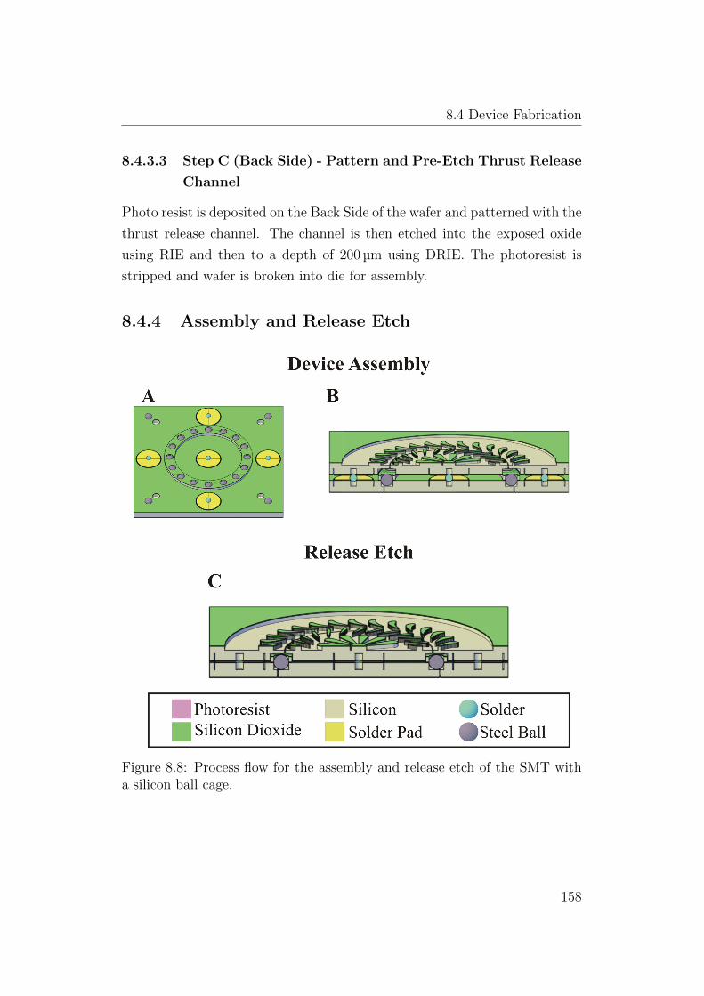
8.4 Device Fabrication
8.4.3.3 Step C (Back Side) - Pattern and Pre-Etch Thrust Release
Channel
Photo resist is deposited on the Back Side of the wafer and patterned with the
thrust release channel. The channel is then etched into the exposed oxide
using RIE and then to a depth of 200 µm using DRIE. The photoresist is
stripped and wafer is broken into die for assembly.
8.4.4 Assembly and Release Etch
Figure 8.8: Process flow for the assembly and release etch of the SMT witha silicon ball cage.
158

8.4 Device Fabrication
8.4.4.1 Step A - Place Cage, Solder Balls, and Steel Balls in
Thrust Die
A thrust side die is placed on a surface and the solder pads are painted with
solder flux. 300 µm diameter solder balls are placed at the center of the solder
pads and are held in place by the solder flux. A cage is then placed over the
raceway. The ball pockets are then filled with the steel balls. A SEM image
of the thrust die after this assembly process is shown in Figure 8.9.
Figure 8.9: SEM of the 5 mm diameter SMT after the all of the parts havebeen assembled on the thrust die but before the turbine die has been placedon top.
8.4.4.2 Step B - Align Turbine Die and Bond the Device
The turbine die is attached to the vacuum chuck of a custom bonder/aligner.
The assembled thrust die is placed under the turbine die, the die are aligned
and then brought into contact under light force. A butane torch is then used
to rapidly heat the die, causing the solder to reflow and bonding the die. The
bonded device is then removed from the bonder and allowed to rapidly cool
on a metal surface.
159
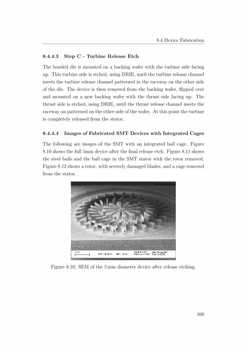
8.4 Device Fabrication
8.4.4.3 Step C - Turbine Release Etch
The bonded die is mounted on a backing wafer with the turbine side facing
up. This turbine side is etched, using DRIE, until the turbine release channel
meets the turbine release channel patterned in the raceway on the other side
of the die. The device is then removed from the backing wafer, flipped over
and mounted on a new backing wafer with the thrust side facing up. The
thrust side is etched, using DRIE, until the thrust release channel meets the
raceway on patterned on the other side of the wafer. At this point the turbine
is completely released from the stator.
8.4.4.4 Images of Fabricated SMT Devices with Integrated Cages
The following are images of the SMT with an integrated ball cage. Figure
8.10 shows the full 5mm device after the final release etch. Figure 8.11 shows
the steel balls and the ball cage in the SMT stator with the rotor removed.
Figure 8.12 shows a rotor, with severely damaged blades, and a cage removed
from the stator.
Figure 8.10: SEM of the 5 mm diameter device after release etching.
160

8.5 Testing
Figure 8.11: SEM image showing the Full Ring cage and steel balls in the5 mm SMT stator after rotor has been removed.
Figure 8.12: SEM image of a rotor and cage that have been removed for theSMT stator. The turbine blades have been severely damaged.
8.5 Testing
The devices were tested using the setup described in Section 5.2.2; and was
carried out by driving the SMT with a compressed nitrogen or air supply
while at the same time bleeding gas from the back side of the device to provide
161

8.5 Testing
some control over the normal load on the bearing. In initial performance tests
the input drive power (inlet gauge pressure X volume flow rate) was varied,
and rotation speed, gas flow and input pressure were recorded. This allowed a
performance curve of rotation speed versus input power to be plotted. These
tests could not provide an absolute measure of the bearing losses, since the
turbine efficiency was unknown; however, they did allow comparison between
the bearings with different cage designs. Performance tests were carried out
on two devices for each combination of retainer type and device size. In
addition, the repeatability of results was verified for one device, and longevity
testing was performed on a 5 mm device and a 10 mm device to evaluate wear
during extended operation
To test each device, the bleed valve was first set to a known value. This
value was determined by running a Half Skeleton device at 2 W of input
power and adjusting the bleed valve until the device operated smoothly. This
calibration was performed separately for the 5 mm rotor and 10 mm devices
and the initial valve setting was maintained for all subsequent testing. The
calibration resulted in an upward normal force on the underside of the rotor
of 5 mN to 48 mN for the 5 mm devices and 4.5 mN to 40 mN for the 10 mm
devices over the input power range tested. Each device was then ramped
through a range of inlet pressures at least 3 times to evaluate the performance.
Longevity and wear were evaluated by operating a 5 mm and a 10 mm device
continuously for an extended period of time (up to 12 hours) while counting
the number of revolutions. Open retainer designs were used in these tests.
8.5.1 Comparison of Cage Design Performance
Each type of retainer was tested by increasing the flow of nitrogen in steps
until an input power of 2.5 W was achieved. The flow of nitrogen was then
cut and the ramping was repeated two further times. In order to gain an
adequate comparison for each retainer ring, two devices of each type were
tested from the same fabrication run.
Figures 8.13 and 8.14 show the measured variations of speed with input
power for the 5 mm and 10 mm devices respectively. Six measurements were
162

8.5 Testing
taken at each input power setting, and all data points are plotted to give
an idea of the scatter in the measurements. The results for both the 5 mm
and 10 mm devices indicate that the Full Ring and the Full Skeleton designs
exhibit the best performance (i.e. highest rotation speed for a given input
power) over a wider range of input power, with the Full Ring performing the
best overall. The Half Skeleton, Outer Open and Inner Open designs perform
consistently less well over the same range.
The Full Ring and Full Skeleton consistently showed the lowest losses.
The Full Skeleton retainer performed less well than the Full Ring in both
sizes of device, and the reasons for this are currently unclear. One possibility
is that the lower rigidity of the Full Skeleton retainer makes it more suscep-
tible to dynamic distortions that result in more contact with the raceways.
This could also explain the drop in performance of the 10 mm Full Skeleton
device at higher power levels. This effect would be expected to be more pro-
nounced in the larger device where the retainer is less stiff. The relatively
poor performance of the more flexible design does run counter to results from
previous studies [Weinzapfel 09]. However, the flat raceways on the silicon
bearings make them less constrained and more susceptible to vibration, and
it is not clear that results relevant to conventional bearings should carry over.
Low rigidity may also be a contributing factor to the poor performance
of the Inner Open and Outer Open retainers. These designs also allow the
balls more radial play which is likely to increase interaction between the
balls and the raceway sidewalls. Furthermore, interactions between the balls
and the edges of the pocket openings may lead to increased frictional losses
with the Open designs. Finally, the poor performance of the Half Skeleton
designs is consistent with their having a lower ball fill factor in the raceways
[Nataraj 08].
163

8.5 Testing
Figure 8.13: Performance curves for the 5 mm devices plotted in RPM versusInput Power W.
Figure 8.14: Performance curves for the 10 mm devices plotted in RPM versusInput Power W.
It should also be noted that, because the thrust bleed valve was main-
tained in a fixed position during ramp testing, the turbines may not have
been operating in the most ideal regime. It was verified during tests that the
164

8.5 Testing
bearings were operating in the correct mode, with a net upward thrust on
the rotor. However, it is likely that better performance could be obtained by
re-adjusting the bleed valve during testing to find the optimal performance
regime, and this will be explored in future work.
8.5.2 Performance Repeatability
A 5 mm diameter Full Ring device was run through successive ramp tests,
averaging 30,000 revolutions per ramp, to evaluate the repeatability of the
results. For each ramp test, the measured variations of rotation speed with
inlet power were averaged, and then simple linear interpolation was used
to estimate the rotation speed at fixed power levels of 0.5 W, 1.0 W, and
1.5 W. Figure 8.15 shows how the rotation speed at each of these power levels
varied over the first 12 runs. At all power levels, an initial improvement in
performance was observed, followed by a fall-off up to round the 8th run,
beyond which the rotation speed was stable to within ±10%. It is believed
that the initial improvement is due to removal of asperities on the bearing
surfaces, while the subsequent fall occurs as the sides of the bearing raceway
become worn making the bearing less stable due to increased play in the
rotor position.
165

8.6 Longevity and Wear
Figure 8.15: Measured repeatability of performance over 12 ramp tests for a5 mm Full Ring Device operating at difference power levels.
8.6 Longevity and Wear
Longevity was evaluated by running a 10 mm diameter device with an Outer
Open retainer and a 5 mm diameter device with an Inner Open retainer for
extended periods of time. The retainers with the lowest mechanical strength
were chosen for this test as one of the aims was to induce early failure and
identify the failure mode. However, both devices survived the longevity test-
ing without failure and only required minimal cleaning to resume operation if
the bearing became locked. Just over 2.5 million revolutions were logged for
the 10 mm diameter device and just over 2.98 million revolutions were logged
for the 5 mm diameter device. The devices were disassembled for inspection
by heating the tested device to above the melting point of the solder to break
the solder bonds.
Wear effects on the bearing raceways after longevity testing were similar
to those described in [McCarthy 09] and [Hanrahan 10]. There was some ball-
induced wear on the sidewalls of the bearing raceway, and narrow wear tracks
could be seen in the silicon raceway surfaces top and bottom, as shown in
Figure 8.16. The retainers in both devices experienced minimal wear on their
166

8.6 Longevity and Wear
upper surfaces during operation. For example, Figure 8.17 is an SEM image
showing the upper surface of the 5 mm Inner Open retainer. An optical
profilometer scan indicated that the contact wear on the retainer did not
exceed 1 µm on any portion of the ring. This was also confirmed using a
microscope, by observing that silicon dioxide was still present in most of the
wear regions. The edge of one of the ball pockets also shows some signs of
damage likely attributable to shock during start up of the device.
The undersides of the retainers showed wear around the edges of the ball
pockets due to abrasion by the balls, as shown in Figure 8.18. This has
the effect of increasing the effective pocket size, and relaxing the constraints
imposed on the balls by the retainer.
Figure 8.16: SEM images of the raceway wear on the rotor (top image)and the stator (bottom image) of the 10 mm diameter device after longevitytesting.
167

8.7 Discussion and Conclusions
Figure 8.17: SEM image showing the wear (indicated by the arrows) on thetop of the retainer after longevity testing.
Figure 8.18: SEM image showing the wear on the bottom of the retainerafter longevity testing.
8.7 Discussion and Conclusions
This chapter presented the exploration of several different geometries of sili-
con retainer rings integrated into a SMT with a thrust ball bearing, at rotor
168

8.7 Discussion and Conclusions
diameters of both 5 mm and 10 mm. Full Ring retainers, which are an annu-
lar design with cylindrical ball pockets, were found to perform better than
designs with pockets that were open on one side, even though the latter
had lower contact area with the bearing rings. Removal of material from
the Full Ring design while retaining the cylindrical pocket shape was also
found to degrade performance. The SMT with the Full Ring retainer could
operate at over 20 000 RPM with less than 2 W of input power. Also 5 mm-
and 10 mm-diameter devices were able to operate for over 2.5 million revo-
lutions without device failure. Further investigation will need to be carried
out to fully characterize the performance of each design and to understand
the effects of retainer and raceway wear on the bearing performance. Future
work will include measuring the bearing vibration, observing the lateral dis-
placements of the turbines during operation and finding the optimal running
conditions for the turbine by varying the thrust bleed rate. Design improve-
ments will include exploring softer retainer materials such as polymers and
metals; exploring new ball materials; and improving the bearing geometry by
moving the retainer to the center of the ball and creating a curved raceway
to allow for better self-center of the bearing during operation.
169
Chapter 9
Curved Raceway
A curved raceway can support higher normal loads than a similar rectangular
raceway. This design can also be used to create self centering ball bearings
similar to those found at the macro-scale. This chapter will present the design
and fabrication of the devices used to explore the viability of integrating
the angular contact raceway into silicon MEMS rotary ball bearings. The
raceway is created by using the isotropic properties of inductively coupled
plasma (ICP) as found in deep reactive ion etching (DRIE) systems when
passivation cycles are removed from the processing. The micro-tribometer
and silicon micro-turbines (SMTs) were both used in this study to evaluate
the bearings. Results will be presented for the bearing performance in terms
of power loss, as well as for the longevity and wear.
9.1 Device Design
Two classes of curved raceway bearing were developed for this study: one
designed for evaluation using the micro-tribometer, and another that was
integrated into an SMT with a 5 mm diameter rotor. The novelty in these
devices lay in the fabrication of the bearing raceway. As there was no inte-
grated ball cage, there were fewer design constraints and geometric consider-
ations than seen in the radial design described in Chapter 6. The fabrication
process for the SMTs was also greatly simplified over the devices presented
170

9.1 Device Design
in Chapter 8 as the raceway did not have the stepped profile needed for an
integrated ball cage.
Figure 9.1: SEM of micro-lens mold with a diameter of 116.7 µm createdusing HNA etching, picture from [Albero 09].
Figure 9.2: SEMs of the curved profile created by the ICP method, picturefrom [Larson 05].
The primary design challenge for these devices was creating a curved
raceway profile that was suitable for a ball with a 500 µm diameter. Curved
geometries have been created previously in silicon for micro-lens molds. For
171

9.2 Device Fabrication
example, in [Albero 09] a wet etch process is used to create spherical molds as
shown in Figure 9.1. In [Larsen 05] an ICP etch is used to create the micro-
lens shape. This is very similar to the desired profile of the angular contact
raceway and is shown in Figure 9.2. The ICP process has the advantage
of being easily integrated into existing fabrication process flows described in
this thesis, therefore it was deemed the most efficient method for creating
the angular contact raceways. The special requirements for this process step
will be covered in the following section.
9.2 Device Fabrication
This section will describe the device fabrication process flows for each of the
two classes of device. Simplified process flows are presented here; for more
details on the processes used please refer to Chapter 3.
9.2.1 Fabrication of SMTs with Angular Contact Race-
ways
The SMTs with angular contact raceways were fabricated from 100 mm di-
ameter, p-type, <100>, DSP silicon wafers with a thickness of 525±25 µm.
The wafers also had 1 µm of thermally grown silicon dioxide. A seed layer
of chrome and copper was deposited on the wafer (and is not shown in the
process flow) for electroplating the solder pads. A description of each pro-
cessing step follows. The steps are labeled with the letter corresponding to
the depiction of the step in Figure 9.3.
9.2.1.1 Bearing Raceways
The wafer is plated with eutectic solder pads and the curved raceways are
then etched into the silicon substrate. The steps for these processes are listed
below with the letter corresponding to the step depicted in Figure 9.3
9.2.1.1.1 Step A - Plate Solder Pads
The wafers are coated with photoresist and patterned with the solder pad
172

9.2 Device Fabrication
Figure 9.3: Device fabrication process flow for SMTs with angular contactraceways.
173

9.2 Device Fabrication
mask. The solder pads are electroplated with a 2 µm nickel diffusion barrier,
3 µm of tin and 300 nm of gold. The photoresist is then stripped and the
exposed seed layer (not shown in the diagram) is etched to expose the silicon
dioxide below.
9.2.1.1.2 Step B - Define Raceway Width
The wafer is coated with photoresist and a mask is used to define the
desired width of the raceway (505 µm.) The exposed oxide is etch using RIE
and the photoresist is stripped from the wafer. This pattern is used during
the isotropic etch step to monitor the width of angular contact raceway.
Ensuring that the raceway reaches the minimum desired width at the end of
the etching cycle.
9.2.1.1.3 Step C - Pattern Raceway Isotropic Etch Mask
The wafer is coated with photoresist. The raceway isotropic etch mask is
used to pattern a track that is half the width of the final raceway (250 µm.)
The pattern is half the desired width to account for the isotropic nature of
the etch. The etch (described in the next step) will undercut the photoresist
mask and producing a toroidal geometry that is 250 µm deep and 500 µm
wide.
9.2.1.1.4 Step D - Raceway Isotropic Etch
The raceway feature patterned in the previous step is etched using a DRIE
in an ICP configuration. The DRIE parameters used to etch the raceways can
be found in Table 9.1. After etching the raceway, the photoresist is stripped
from wafer.
It should be noted that the photoresist is the only mask used in this etch
process. It was found that even with bending in the photoresist, from the
excessive undercut, the etch maintained a toroidal geometry.
9.2.1.2 Turbine Side
After the solder pads are deposited and the raceway is etched, the turbine
is defined on the other side of the wafer. The process steps for defining the
174

9.2 Device Fabrication
Parameter ValueEtch Time 90 minSF6 flow rate 130 sccmO2 flow rate 13 sccmRF power 600 W
RF frequency 13.56 MHzPlaten Power 5 wattAPC setting 60% (manual)
Table 9.1: DRIE process parameters for etching the angular contact raceway.
turbine are listed below with the letter corresponding to the step depicted in
Figure 9.3.
9.2.1.2.1 Step E - Define Turbine Blades in Oxide
Photoresist is deposited on the wafer and patterned with the turbine
blades. The blade design is then transferred to the wafer by etching the
exposed oxide. The photoresist is then stripped from the wafer.
This pattern will be used as an etch mask during the turbine blade etch
and device release step (Section 9.2.1.4.2 or Step I.) An oxide mask is required
because it can survive the assembly process and high temperatures of the
solder reflow (Section 9.2.1.4.1 or Step H.)
9.2.1.2.2 Step F - Etch Turbine Journal After the turbine blades are
defined, a new layer of photoresist is deposited on the wafer. The turbine
journal is patterned and etched to a depth of approximated 175 µm. This
depth accounts for the etch lag during the turbine blade etch and device
release step (Section 9.2.1.4.2 or Step I.) After this step, the photoresist is
stripped and the wafer is broken into individual die for assembly.
9.2.1.3 Thrust Side
After the solder pads are deposited and the raceway is etched, the thrust
journal is defined on the other side of the wafer. The process step for defining
the thrust journal is listed below with the letter corresponding to the step
175

9.2 Device Fabrication
depicted in Figure 9.3. This will then become the bottom wafer in the bonded
device stack.
9.2.1.3.1 Step G - Define Thrust Journal Photoresist is deposited
on the wafer and patterned with the thrust journal. The oxide is then etched
using RIE to defined the thrust journal. The wafer is then loaded into the
DRIE and the thrust journal is etched to a depth of 175 µm. After this step
the photoresist is stripped and the wafer is broken into individual die for
assembly. The oxide remaining on the thrust side of the wafer will be used
as an etch mask during the final release etch (Section 9.2.1.4.2 or Step I.)
9.2.1.4 Device Assembly
After the turbine and the thrust sides of the device have been fabricated, the
device can be assembled. After assembly the oxide masks created in previous
steps are used to define the turbine blades and release the turbine rotor from
the stator. The process steps for the device assembly and release are listed
below with the letter corresponding to the step depicted in Figure 9.3.
9.2.1.4.1 Step H - Placement of Steel Balls, Solder Balls, Die
Alignment and Solder Reflow
The device is assembled in a custom aligner/bonder. The raceway of thrust
die of the device is filled with the desired number of steel balls. Solder flux
is then painted on to the solder pads using a fine tip paint brush; this serves
to inhibit oxidation of the solder pads and to hold the solder balls in place.
300 µm diameter solder balls are then placed on the centers of the solder pads.
The turbine die of the device is attached to a vacuum chuck and aligned to
the thrust side of the device in a custom bond aligner. A force is applied
to the top of the turbine side to hold the alignment position of the die and
encourage a uniform reflow of the solder. The device is heated with the flame
from a butane torch for 30 s. The force is removed, the device is removed
from the aligner/bonder and is cooled on a metal surface.
176

9.2 Device Fabrication
9.2.1.4.2 Step I - Release Etches
The bonded devices from the previous step (Section 9.2.1.4.1 or Step H)
are mounted to a backing wafer with the turbine side facing up. The device
is etched using DRIE until the turbine journal reaches the raceway below.
This results in a turbine blade height of 150 µm to 175 µm. The devices are
then detached from the backing wafer, cleaned and remounted to a backing
wafer with the thrust side of the device facing up. The thrust journal is
then etched until it reaches the raceway. For both of these steps the oxide
patterned in previous steps is used as the etch mask. These final etch steps
define the turbine blades and release the turbine rotor from the stator.
9.2.2 Fabrication of Devices for Tribometer Testing
The ball bearings with angular contact raceways for tribometer testing were
fabricated from 100 mm diameter, p-type, <100>, DSP silion wafers with a
thickness of 525±25 µm. The wafers also had 1 µm of thermally grown silicon
dioxide. A seed layer of chrome and copper was deposited on the wafer (not
shown in the process flow) for electroplating the solder pads. A description
of each processing step follows the step letter corresponding to the depiction
of the step in Figure 9.4.
9.2.2.1 Bearing Raceway
The bearing raceway is fabricated in the same way as the raceway for the
angular contact SMT devices. Please see Section 9.2.1.1 for more details. The
process steps are depicted in Figure 9.4 and letter for each step corresponds
with the label in the figure.
9.2.2.1.1 Step A - Plate Solder Pads
See Section 9.2.1.1.1 for more details.
9.2.2.1.2 Step B - Define Raceway Width
See Section 9.2.1.1.2 for more details.
177

9.2 Device Fabrication
Figure 9.4: Device fabrication process flow for devices with angular contactraceways for tribometer testing.
178
9.2 Device Fabrication
9.2.2.1.3 Step C - Pattern Raceway Isotropic Etch Mask
See Section 9.2.1.1.3 for more details.
9.2.2.1.4 Step D - Raceway Isotropic Etch
See Section 9.2.1.1.4 for more details.
9.2.2.2 Backside
The backside of the device, or the side of the device that does not connect
to the testing adaptor is fabricated with the steps indicated below. These
steps result in features of 2 different etch depths and leave an oxide mask
for the final release etch after assembly. The letter for each step corresponds
with the depiction of that step in Figure 9.4. For the DRIE steps the wafer
is mounted to a backing wafer; this is not shown in Figure 9.4.
9.2.2.2.1 Step E - Define Device Edge
Photoresist is spun on the back of the wafer after the bearing raceway has
been patterned. The Photoresist is patterned with the edge features of the
device (the feature that will release the device from the die.) The exposed
oxide is etched using RIE and the photoresist is stripped from the wafer.
9.2.2.2.2 Step F - Pre-Etch Device Edge
Photoresist is spun on the wafer. The wafer is patterned with the device
edge and the bearing back side rotor release channel. The device edge is
then etched to a depth of approximately 250 µm. The backside rotor release
channel will not be etched due to the oxide mask. The photoresist is not
stripped from the wafer after this step as it will continue to be used as a
mask in the next step.
9.2.2.2.3 Step G - Define and Pre-Etch Rotor Release Channel
The exposed oxide (covering the rotor release channel in the previous step)
is etched using RIE. The rotor release channel and the device edge are then
etched using DRIE. The rotor release channel is etched to a depth of 200 µm,
while the device edge typically reaches a final depth of around 400 µm due to
179

9.2 Device Fabrication
etch lag. The photoresist is stripped and the wafer is broken into individual
die for device assembly.
9.2.2.3 Adaptor Side
The adaptor side of the device has an adaptor port which allows the device to
be coupled to the tribometer. Further, in order to easily identify the thrust
style and radial style bearings, the radial bearing has a label as shown in the
process depicted in Figure 9.4. The letter for each step corresponds with the
depiction of that step in Figure 9.4. For the DRIE steps the wafer is mounted
to a backing wafer, this is not shown in Figure 9.4.
9.2.2.3.1 Step H - Define Device Edge and Device Label
Photoresist is spun on the wafer. The wafer is patterned with the device
label and the device edge. The exposed oxide is etched using RIE and the
photoresist is then removed from the wafer.
9.2.2.3.2 Step I - Pre-Etch Device Edge
Photoresist is spun on the wafer. The wafer is patterned with the device
edge, the adaptor port feature and the rotor release channel. The device edge
is then etched to a depth of 250 µm. The photoresist is not stripped after
this step as it will be used in the next step.
It can be seen that the device label is covered by the photoresist in this
step. This will allow us to pattern and etch the other features while protecting
the label from etching until the final release etch. This allows us to create 3
different etch depths with only 2 masks.
9.2.2.3.3 Step J - Define and Pre-Etch Rotor Release Channel and
Testing Adaptor Feature
The exposed oxide from the previous step is etched using RIE. The wafer is
then etched using DRIE. The rotor release channel and the adaptor port are
etched to a depth of approximately 200 µm, while the device edge typically
reaches a final depth of around 400 µm due to etch lag. The photoresist is
removed and the wafer is broken into die for assembly.
180

9.2 Device Fabrication
9.2.2.4 Device Assembly
9.2.2.4.1 Step K - Placement of Steel Balls, Solder Balls, Die
Alignment and Solder Reflow
The device is assembled in a custom aligner/bonder. The raceway of adap-
tor side of the device is filled with 7 steel balls. Solder flux is then painted
on to the solder pads using a fine tip paint brush, this serves the purposed of
removing oxidation from the solder pads and to hold the solder ball in place.
300 µm diameter solder balls are then placed on the center of the solder pads.
The Backside of the device is attached to a vacuum chuck and aligned to the
adaptor side of the device in a custom bond aligner. A force is applied to
the top of the backside of the device to hold the alignment position of the
die and encourage a uniform reflow of the solder. The device is heated with
the flame from a butane torch for 30 s. The force is removed, the device is
removed from the aligner/bonder and is cooled on a metal surface.
9.2.2.4.2 Step L - Release Etch
Patterned oxide from previous steps will be used as the DRIE mask in this
step. After assembly, the die are mounted to a backing wafer (not shown
in Figure 9.4) with the adaptor side facing up. The device is then etched
using DRIE until the rotor release channel reaches the raceway below, and
the device edge reaches the back of the wafer. The device label will also
be etched to a depth of approximately 150 µm and the adaptor feature is
etched an additional depth of approximately 125 µm. After DRIE processing
the device is removed from the backing wafer, flipped over to explose the
backside of the device, and mounted to a backing wafer for DRIE processing
of the backside. The device is eched until the rotor release channel reaches
the raceway below and the device edge reaches the back of the wafer. The
wafer is then removed from the backing wafer.
9.2.2.4.3 Step M - Remove Device from Die
After the final release etches, the device is removed from the die. The
device is completely separated from the die at this point and can be easily
lifted from the surrounding silicon. Five devices are present on each die,
181

9.2 Device Fabrication
and when separated from the die look like the device labeled M in Figure
9.4. The device can now be inserted into the tribometer test platform for
characterization.
9.2.3 Images of Fabricated Devices
This section contains images of the fabricated devices. Figure 9.5 shows a
rotor from a device used for tribometer testing. A steel ball that has been
through testing is located next to the device to show the raceway curvature
in relation to the ball in the design. A similar SEM for the SMT rotor is
shown in Figure 9.6. In the image some fabrication damage can bee seen
on the raceway of the rotor. This damage was present on all of the devices
fabricated with the current process, and was caused by over-etching during
the bearing release etch step. Figure 9.7 shows a close up of the worst of the
damage on a SMT stator raceway. This damage is only present where the
balls are not located in the raceway during the release etch. Further studies
will make an effort to protect the raceway from this damage. Figure 9.8
shows how the raceway should look without any of the over-etching damage.
The raceway is extremely smooth and has the desired curved geometry.
Figure 9.5: SEM image of a rotor used for tribometer testing. A steel ballhas been placed next to the rotor to show the curvature of the raceway inrelation to the ball used in the device.
182

9.2 Device Fabrication
Figure 9.6: SEM image of the SMT rotor with a ball next to the raceway toshow the curvature of the raceway in relation to the ball.
Figure 9.7: SEM image of a SMT stator raceway. The large depression onthe raceway are damage for over-etching during the release etch step.
183

9.3 Performance
Figure 9.8: SEM image of a stator raceway with the ideal geometry and noetch damage.
9.3 Performance
The performance of the angular contact raceway was evaluated by testing
the SMTs and the devices in the tribometer. The SMT devices were used to
evaluate the longevity of the bearings at high speeds. The tribometer was
used to evaluate the bearing loss under controlled conditions. The following
sections will describe the results of these tests.
9.3.1 Performance of SMT with Angular Contact Race-
way
The SMT was run for a total of 10 million revolutions. Ramp tests were per-
formed on the SMT before any longevity testing and then after ever 2 million
revolutions. The longevity tests were run at speeds of up to 70 000 RPM.
These speeds were achieved by adjusting the bleed valve and the input pres-
sure until the turbine was able to run smoothly at the higher speeds. This was
primarily to reduce the duration of the longevity tests and to rapidly stress
test the bearing in the turbine. The graph in Figure 9.9 shows that after an
initial improvement in performance after 2 million revolutions the bearing
184

9.3 Performance
performance starts to decrease. As will be seen in Section 9.3.3 the raceway
shows minimal wear after testing. When compared to the performance of
the 5 mm diameter SMT with the Full Ring retainer, presented in Chapter
8, the curved raceway under performs the bearing with the retainer at lower
speeds as shown in Figure 9.10. This would be the case if the centrifugal
forces on the balls dominates the power loss in the bearings as the Full Ring
design has only 16 ball and the curved raceway has 25 balls. The curved
raceway, however, does out perform the Full Ring bearing at higher input
powers which is contradictory to what we would expect. This performance
difference may have more to do with the turbine design and the differences
in the blade heights for devices. The blade height for the Full Ring turbine
was approximately 650 µm where the blade height for the curved raceway
was approximately 125 µm.
Figure 9.9: Graph of the speed and input power of the SMT after each 2million revolution longevity test. After an initial improvement in performanceafter 2 million revolution, the turbine performance begins to decline.
185

9.3 Performance
Figure 9.10: Comparison of the performance of the 5 mm SMT with the FullRing and the curved raceway SMT.
9.3.2 Tribometer Measurements
The bearings tested in this study had a radial bearing design much like the
bearings described in Chapter 6 but without a cage. The bearings also had
7 balls in the raceway to give a fill factor (F%) of approximately 74% and
dm of 1.25 mm. The bearings were tested in 50 RPM speed increments from
50 RPM to 2500 RPM. The normal load for these tests was set to 40 mN.
Figure 9.11 shows the raw measurements for the 3 tests. As seen in the
graph the measurements had a relatively wide spread.
If Equation 6.1 is used to predict the frictional torque we find the the
calculation for Ml is a good estimate for this bearing. However, the pre-
dicted centrifugal torque 9 times lower than the measured torque. However,
the frictional torque (even with the wide spread) does conform to a change
proportional to ω2 as is expected for an increase in frictional torque due to
the centrifugal force of the balls.
A further observation is that if it is assumed that the only influence on
increase in the bearing frictional torque is the number of balls the relation-
186

9.3 Performance
ship between the radial bearing and the curved raceway bearing could be
expressed as:
M = e0.75Nb
7 Mc −Ml (9.1)
This is using z = 0.8 to calculate Ml. However, since there are several
other aspects that differ in the bearings such as the lack of a cage in the
curved raceway bearing and the different raceway geometries, this is simply
an observation of the relation of the two designs.
The power loss varies by ω3 as expected. The predicted value based using
Equation 9.1 to calculate M is plotted in Figure 9.12 with the power loss
calculated using the average of the measured data.
Figure 9.11: Graph of the tribometer results for the angular contact bear-ings. The line represents the expected torque value for the devices and themeasured data points for 3 tests are scattered plotted on the graph
187

9.3 Performance
Figure 9.12: The power loss predicted by using Equation 9.1 to calculatethe frictional torque and the power loss calculated using the average of themeasured frictional torque.
9.3.3 Wear
Both the SMT and the tribometer devices showed very little wear on the
raceways after testing. The SMT survived over 10 million recorded revolu-
tions with speed up to 70 000 RPM and still showed minimal wear. As the
curved raceway allows the load on the ball and the raceway to be spread over
a larger area less wear would be expected on the raceway. Figure 9.13 shows
the stator of the tested turbine with arrows indicating the over-etch damage
on the raceway and with the wear region indicated by a box. The wear is
seen as lighter areas within the box. The wear, which is very difficult to see,
appears as small lighter areas on the raceway. The raceway of the device
tested with the tribometer showed no detectable wear pattern.
188

9.4 Discussion and Conclusions
Figure 9.13: SEM image of the tested SMT stator raceway. The wear patternis enclosed in the box and the over-etch damage to the raceway is indicated bythe arrows. The wear can be identified as the lighter regions on the racewayregion enclosed by the box.
9.4 Discussion and Conclusions
The curved raceway was successfully incorporated into both SMT and tri-
bometer designs. The SMT was able to survive over 10 million revolutions
at prolonged speeds of up to 70 000 RPM and showed minimal signs of wear
on the bearing raceway. However, the performance of the turbine does show
a steady decline after 2 million revolutions, which may be attributable to
excessive wear on the balls. The curved raceway SMT performed worse than
the SMT with the Full Ring retainer at lower input power, as would be ex-
pected if the the centrifugal force on the balls is the dominant cause of losses
in the bearing as the curved raceway had 25 balls and the SMT with the
full ring had 16 balls. However, at higher input power the curved raceway
did start to perform better than the SMT with the Full Ring retainer. This
may have been due to the difference in the turbine blade heights or it may
have been due to the geometry of the raceway, further testing on devices with
similar blade heights will need to be carried out to determine the cause of
this phenomenon.
189

9.4 Discussion and Conclusions
The tribometer measurements showed frictional torque 9 times greater
than the torque that was estimated by the Equation 6.1 for the radial bearing
in Chapter 6. A higher frictional torque was expected for this design as 7 balls
were in the test device rather than the 4 in the radial design. A relationship
is provided for the difference in measured torque relating only to the number
of balls in Equation 9.1. However, this is a rather naive modification that
ignores other factors such as the lack of a cage in the curved design and the
new raceway geometry. However, estimate for Ml as calculated in Equation
6.1 does conform to the measured values for this design.
Additional work will need to be done to remove the release etch damage
from the the curved raceway and to characterize any advantage of using
the curved raceway geometry. The design does allow for the creation of self
centering bearings and there appeared to be less wear on the curved raceways
went compared to the rectangular raceways.
190

Chapter 10
Conclusions and Further Work
This chapter will present an overview of the contributions of the thesis and a
review of the research objectives. A brief overview of some of the conclusions
reached through completing the work will also be provided, and future work
will be proposed.
10.1 Contributions of this Thesis
This thesis provides an investigation of new fabrication techniques and ge-
ometries for use in micro-ball bearings for MEMS applications. The work
presented here showed the first integration of ball cages into MEMS ball
bearing designs. The investigation of the fabrication and design constraints
will be useful in guiding future designs. Further, the observation of the ef-
fects of centrifugal force on the performance and the overall loss within the
bearing has not been previously presented for bearings on this scale. The
frictional torque related to the bearing load was found to be 1000 times
greater for micro-bearing compared to the predicted value for macro scale
bearings. Also, the measured friction torque increased with ω2 confirming
that the centrifugal force of the balls plays a significant role in the bearing
loss at higher speeds. It should be noted that the equation used to predict
the frictional torque was extremely simplistic and it under estimated the fric-
tional torque for the bearings presented in this thesis. Further, this thesis
191

10.2 Objectives Revisited
presents new fabrication techniques and designs that can be used in future
micro-ball bearing designs.
10.2 Objectives Revisited
In the introduction a list of research objectives was presented to provide an
overview of the overall goals of this thesis. Each objective will be revisited
here with a brief discussion how the objective was met and the results of the
investigation presented in the preceding chapters.
1. Characterize the performance of the devices designed for this study by
modifying and improving, where possible, existing testing methodolo-
gies (Chapter 5.) This objective was met by using the existing micro-
tribometer and the SMT designs. Data acquisition and gas flow con-
trol were improved in the SMT setup to provide accurate and simple
measurement techniques not available in earlier similar research. The
micro-tribometer was used as designed. Devices were designed to allow
coupling of the driving motor and mounting into existing test platforms.
Test platforms were modified by the author to allow for configuration
of the measurement range and to improve device yield. The capabilities
of each of the test platforms is:
Tribometer: It is possible to resolve torque measurements down to
1 µN m with the current platform configuration with maximum measur-
able torque of 100 µN m. The maximum measurable torque is config-
urable by increasing the number of beams attached the to test platform.
The normal load has a measurement resolution of 5 mN and can applied
reliably in 10 mN increments. The speed can be set in increments of
1 RPM of the range of 0 RPM to 30 000 RPM. Measurement acquisition
is configurable in 1 s increments. The testing range and measurement
resolution of this system are sufficient provide insight into the losses in
the micro-bearings. The system also has the added benefit of showing
when the bearing is operating in rolling or sliding friction.
192

10.2 Objectives Revisited
SMT Setup: The turbine is a fully integrated MEMS solution for test-
ing the bearing technologies. The input power can be measured and
controlled in 5 mW increments. The force on backside of the turbine
can be measured in 5 mN increments. Speed can be resolved up to
200 000 RPM with a resolution of 1/12 of a revolution. The data acqui-
sition can also be configured to capture data in increments of 100 ms
and with data storage of 2GB testing can be performed for multiple
days without interruption. Also, testing can be performed in a fully au-
tomated mode including the ramping up and down of the input power.
The tribometer testing provided the measurement resolution needed to
confirm that the centrifugal force is the dominant source of the losses
in the ball bearings. While the SMT allowed for prolonged testing of
the bearings at high speed, while demonstrating the bearing design as
a fully integrated part of a MEMS device.
2. Design and integrate a ball cage into a MEMS micro-ball bearing us-
ing the simplest technique possible (Chapter 6.) The design technique
presented provides a simple method of incorporating a ball cage into a
micro-ball bearing. This design reduced the overall bearing fill factor
and the centrifugal force related bearing loss over comparably sized de-
vices without a cage as presented in Chapter 9. The limitation of this
design was primarily in the failure of the cage bond interface. This was
due to poor reflow during the bond process and also due to failure of
solder pad due to poor adhesion with the silicon. This cage weakness
led to the further studies of single crystalline silicon cages. However,
this design provided insight into the power loss in the bearings. As
it was observed that the frictional torque due to the applied load was
1000 times higher than that predicted for macro-scale bearings. It was
also observed that the frictional torque increased with ω2 as would be
expected if the centrifugal force of the balls played a dominant role in
the bearing loss. When comparing the measured frictional torque to
the simplified model it was discovered that the measured values were 3
times greater than the value predicted by the model.
193

10.2 Objectives Revisited
3. Design a fabrication technique for releasing moving parts from MEMS
devices with multiple layers (Chapter 7.) This fabrication technique
- using DRIE to remove sacrificial beams embedded in a multi-wafer
stack - was intended to improve the micro-ball bearing performance by
allowing for the in situ fabrication of a single crystalline ball cage. The
dual row cage design was not as efficient as the previous design. Though
the cage design was not optimal, the fabrication technique does prove to
be viable for aligned multi-level MEMS application such as gear stacks
and other complex mechanics.
4. Integrate a ball cage into a working MEMS device with a micro-ball
bearing support mechanism (Chapter 8.) The SMT was used to ex-
plore 5 different single crystalline ball cages. The cages were inserted
manually in this application but could be integrated using the tech-
nique demonstrated in Chapter 7. The hope was to demonstrate a
lower bearing loss than present in a cageless bearing by reducing the
centrifugal force of the balls. The devices did not necessarily demon-
strate an improved performance. However, testing indicated that the
Full Ring ball cage provided the best performance and should likely be
used in further investigations. The results of this study indicate that
the rigidity of the cage is the most important factor in the design.
5. Create a micro-ball bearing raceway with a curved geometry that will
allow for the bearing to self-center and to better mimic race geome-
tries found in conventional macro-scale bearings (Chapter 9.) The
curved raceway was created with an optimized isotropic etching recipe.
The tribometer tests provided frictional torque measurements that con-
firmed the modified calculation ofMl using z=0.8 (rather than 0.0008 as
in macro-scale bearings.) However, the centrifugal torque was 9 times
greater than values predicted by the modified model. These results
point to the need to further improve the model. However, the measure-
ments did confirm that the frictional varied with ω2, further confirming
the role of the centrifugal force as a dominant factor in the bearing loss.
The SMT tests showed that the bearing could survive speeds of up to
194

10.3 Conclusions
70 000 RPM for prolonged periods and that after 10 million revolutions
the bearing was still able to reach speeds of 25 000 RPM with an in-
put power of 2.5 W. It was also observed that the performance of the
curved raceway SMT under performed the SMT with the Full Ring
retainer for input powers below 2 W, which would be expected if the
centrifugal force from the balls in the bearings was the most significant
factor in the power loss in the bearing. However at higher input powers
the curved raceway started to perform better than the SMT with the
Full Ring retainer which requires more exploration.
10.3 Conclusions
This work has shown that it is possible to integrate a ball cage into MEMS
micro-ball bearings. This will be useful for future bearing designs by helping
to reduce bearing losses due to centrifugal forces at intermediate speeds. The
observation of the effects of centrifugal force on the bearing performance
provides insight into the limitations of the micro-ball bearing for high speed
applications. However, the micro-ball bearing has the advantage of providing
high stability; it can also support higher loads and can be integrated into
a device with a simple design with no need for external control systems.
The ability to integrate the bearing in complex micro-mechanical has also
been shown by developing fabrication techniques that can allow for multiple
layers of moving parts. The designs and fabrication techniques presented in
this thesis can be extended for use in multiple applications such as medical
devices, micro-robotics and micro-motors. The research presented in this
thesis provide a basis for creating truly intricate and complex micro-machines.
10.4 Further Work
There were several aspects of the dynamics and the design of the micro-ball
bearings that were not explored in this thesis. Some of these aspects warrant
additional exploration. The following is a list of additional aspects of the
195

10.4 Further Work
bearings that could be explored with the designs that are presented here:
Hysteresis This is a commonly observed phenomenon in ball bearing sys-
tems. Due to the configuration of the test equipment for the micro-
tribometer and the SMT test setup, hysteresis was not studied in the
bearings presented here. Positional, frictional and torque hysteresis
could be characterized for the devices in future studies which would
help to provide models for speed and positional control systems for
systems with micro-ball bearings.
Curved Raceway with Ball Cage A thrust or radial ball bearing could
be created with both a curved raceway and a ball cage. Though the
design of such a bearing would be much more complex than the design
presented in Chapter 6 it would have the advantages of being self-
centering and would have a reduction in the number of balls thereby
reducing centrifugal force losses.
Different Ball Materials Alternative ball materials could improve the per-
formance and the longevity of the bearing. Silicon nitride balls would
reduce the mass and centrifugal force loss in the bearing. Silicon ni-
tride and tungsten carbide could increase the longevity of the balls in
the bearing as balls made from these materials would be stronger than
the 440C steel balls used for the bearings presented in this thesis. Balls
made from these materials are readily available in the sizes needed for
micro-ball bearing designs, but are much more expensive and more
difficult to locate for purchase.
New Cage materials An exploration of new cage materials such as poly-
mers, metals or even glasses could prove to improve cage fabrication
techniques and reduce losses and frictional ball damage associated with
the silicon cages.
Exploration of New Bearing Types With the technique described in Chap-
ter 7 it would be possible to design and fabricate micro-jewel and mag-
netic levitation bearing. The exploration of these bearing types could
196

10.4 Further Work
provide simple designs that operate at higher speeds without the cen-
trifugal losses inherent in the micro-ball bearing designs. The technique
could also be used to create complex gear sets that use either micro-ball
bearings or other bearing designs.
197

Chapter 11
List of Published Works
The following works were published during the course of this research:
• R. Hergert, I.S.Y Ku, T. Reddyhoff, & A.S. Holmes. Micro Rotary
Ball Bearing with Integrated Ball Cage: Fabrication and Characteriza-
tion. In Proceedings of IEEE MEMS Conference, pages 687-690, Hong
Kong, January 24-28 2010.
• R. J. Hergert, B. Hanrahan, A.S. Holmes, & R. Ghodssi. Silicon Re-
tainer Ring Integration in Micro-Turbine with Thrust Ball Bearing Sup-
port Mechanism. In Proceedings of Transducers 2011, Bejing, China,
2011.
• Robert J. Hergert, Brendan Hanrahan, Reza Ghodssi, & Andrew S.
Holmes. Performance of Integrated Retainer Rings in Silicon Micro-
Turbines with Thrust Style Micro-Ball Bearings. Journal of Microme-
chanics and Microengineering. Volume 23, Issue 6,
• R. J. Hergert, W. J. Karl, and A. S. Holmes. Release of Moving Sil-
icon Microstructures Embedded in a Bonded Multi-Wafer Stack Using
DRIE. In Proceedings of Transducers 2013, pages 163-166, Barcelona,
Spain, 16-20 June 2013.
198

Bibliography
[Abraham 08] M. H. Abraham, H. Helvajian & S. W. Janson. LaserAssisted Chemical Ecthing Method for Release Mi-croscale and Nanoscale Devices. United States Patent,no. Patent No. US 7,419,915 B2, Sep 2, 2008.
[Ahmad 09] M. M. Ahmad. Etchant selection for removal of elec-troplating seed layer. Personal Communication, April2009.
[Albero 09] Jorge Albero, Lukasz Nieradko, Christophe Gorecki,Heidi Ottevaere, Virginia Gomez, Hugo Thienpont,Juha Pietarinen, Birgit Paivanranta & Nicolas Passilly.Fabrciation of spherical mircolenses by a combinationof isotropic wet etching of silicon and molding tech-niques. Optics Express, vol. 17, no. 8, pages 6283–6292,13 April 2009.
[Arduino 12a] Arduino. Arduino - ArduinoBoardMega2560.http://arduino.cc/en/Main/ArduinoBoardMega2560,May 2012.
[Arduino 12b] Arduino. Arduino - Home Page. www.arduion.cc, May2012.
[Asay 08] D. B. Asay, M. T. Dugger & S. H. Kim. In-situ vapor-phase lubrication of MEMS. Tribology Letters, vol. 29,no. 1, pages 67–74, 2008.
[Ayon 01] A. A. Ayon, X. Zhang & R. Khanna. Anisotropic Sil-icon Trenches 300-500µm deep eimploying time multi-plexed deep etching (TMDE). Sensor and Actuators A,vol. 91, pages 381–385, 2001.
199

BIBLIOGRAPHY
[Bansal 09] A. Bansal, D. A. Howey & A. S. Holmes. CM-ScaleAir Turbine and Generator for Energy Harvesting fromLow-Speed Flows. In IEEE Transducers, pages 529–532,Denver, CO, USA, 21-25 June 2009.
[Bayt 98] R. L. Bayt, K. S. Breuer & A. A. Ayon. DRIE-Fabricated Nozzles for Generating Subersonic Flows inMicropropulsion Systems. In Proc. of the Solid-StateSensor and Acturator Workshop, pages 312–315, HiltonHead Island, SC, USA, June 1998.
[Beyaz 09] M. I. Beyaz, M. McCarthy, N. Ghalichechian & R. Gh-odssi. Closed-loop control of a long-range microposi-tioner using integrated photodiode sensors. Sensors andActuators A: Physical, vol. 151, pages 187–194, April2009.
[Beyaz 10] M. Beyaz, B. Hanrahan & R. Ghodssi. A Microfab-ricated Rotor Supported On Microball Bearings WithIntegrated Permanent Magnets. In Proceedings of the10th International Workshop on Micro and Nanotech-nology for Power Generation and Energy ConversionApplications (PowerMEMS 2010), pages 167–171, Leu-ven, Belgium, November 30 - December 3 2010.
[Beyaz 12] M.I. Beyaz, B. Hanrahan, J. Feldman & R. Ghodssi.An Integrated Electromagnetic Micro-Turbo-GeneratorSupported on Encapsulated Microball Bearings. InIEEE International Conference on Micro Electro Me-chanical Systems, pages 1209–1212, Paris France, 2012.
[Bhushan 01] Bharat Bhushan, editeur. Modern tribology handbookvolume one principles of tribilogy. CRC Press, BocaRaton, Fla., 2001.
[Chan 11] Mei Lin Chan, B. Yoxall, Hyunkyu Park, Zhaoyi Kang,I. Izyumin, J. Chou, M.M. Megens, M.C. Wu, B.E.Boser & D.A. Horsley. Low friction liquid bearingmems micromotor. In Micro Electro Mechanical Sys-tems (MEMS), 2011 IEEE 24th International Confer-ence on, pages 1237 –1240, Jan 2011.
200
BIBLIOGRAPHY
[Chuang 04] Ricky W. Chuang, Dongwook Kim, Jeong Park &Chin C. Lee. A Fluxless Process of Producing Tin-RichGold-Tin Joints in Air. IEEE Trans. on Componentsand Packaging Technologies, vol. 27, no. 1, pages 177–181, March 2004.
[Chung 04] C.-K. Chung. Geometrical Pattern Effect on SiliconDeep Etching by an Inductively Coupled Plasma Sys-tem. Journal of Micromechanics and Microengineering,vol. 14, pages 656–662, 2004.
[Cohen 10] A. L. Cohen. Micro-Turbines, Roller Bearings, Bushingand Design of Hollow Closed Structures and FabricationMethods for Creating Such Structures. United StatesPatent, no. Patent No. US 7,674,361 B2, March 9, 2010.
[Davis 04] Wyatt O. Davis, Oliver M. O’Reilly & Albert Pisano.On the Nonlinear Dynamics of Tether Suspensions forMEMS. Journal Vibration and Acoustics, vol. 126,no. Issue 3, pages 326–331, July 2004.
[DeltaMask 12] DeltaMask. Welcome to Delta Mask.http://www.deltamask.nl/frames.html, 2012.
[Epstein 04] A. H. Epstein. Millimeter-Scale, Micro-Electro-Mechanical Systems Gas Turbine Engines. Journal ofEngineering for Gase Turbines and Power, vol. 126,pages 205–226, April 2004.
[Fedder 96] G. K. Fedder, S. Santhanam, M. L. Reed, S. C. Eagle,D. F. Guillou, M. S.-C. Lu & L. R. Carley. LaminatedHigh-Aspect-Ratio Microstructures in a ConventionalCMOS Process. Proc. of IEEE International Work-shop on Micro Electro Mechanical Systems, pages 13–18, February 1996.
[Frechette 00] L. G. Frechette, S. A. Jacobson, K. S. Breuer,F. F. Ehrich, R. Ghodssi, R. Khanna, C. W. Wong,X. Zhang, M. A. Schmidt & A. H. Epstein. Demon-stration of a Microfabricated High-Speed Turbine Sup-ported on Gas Bearings. In Solid-State Sensor and Ac-tuator Workshop, Hilton Head Island, SC, USA, June4-8 2000.
201

BIBLIOGRAPHY
[Frechette 05] L. G. Frechette, S. A. Jacobson, K. S. Breuer,F. F. Ehrich, R. Ghodssi, R. Khanna, C. W. Wong,X. Zhang, M. A. Schmidt & A. H. Epstein. High-Speed Microfabricated SIlicon Turbomachinery andFluid Film Bearings. Journal of Microelectromechan-ical Systems (JMEMS), vol. 14, no. 1, pages 141–152,February 2005.
[Freescale 10] Freescale. Integrated Silicon Pressure Sensor On-ChipConditioned, Tempeature Compensated and Calibrated.www.freescale.com, no. Rev 11, March 2010.
[Gabriel 90] K.J. Gabriel, F. Behi, R. Mahadevan & M. Mehre-gany. In situ friction and wear measurements in inte-grated polysilicon mechanisms. Sensors and ActuatorsA: Physical, vol. 21, no. 1-3, pages 184–188, February1990.
[Gad-El-Hak 06] Mohamed Gad-El-Hak, editeur. Mems: Design and fab-rication. Taylor and Fracis Group, Boca Raton, Fla.,2nd edition edition, 2006.
[Garcia 95] E. J. Garcia & J. J. Sniegowski. Surface microma-chined microengine. Sensors and Actuators A: Physical,vol. 48, no. 3, pages 203–214, 30 May 1995.
[Garmire 07] D. Garmire, H. Choo, R. Kant, S. Govindjee, C. H. Se-quin, R. S. Miller & J. Demmel. Diamagnetically Lev-itated MEMS Accelerometers. In IEEE, editeur, Solid-State Sensors, Actuators, and Microsystems Work-shop, TRANSDUCERS 2007, pages 1203–1206, Lyon,France, 10-14 June 2007.
[Ghalichechian 07] N. Ghalichechian, A. Modafe, J. H. Lang & R. Ghodssi.Dynamic characterization of a linear electrostatic mi-cromotor supported on microball bearings. Sensors andActuators A: Physical, vol. 136, no. 2, pages 416–503,May 2007.
[Ghalichechian 08] N. Ghalichechian, A. Modafe, M. Beyaz & R. Ghodssi.Design, Fabrication, and Characterization of a RotaryMicromotor Supported on Microball Bearings. Journal
202

BIBLIOGRAPHY
of Microelectromechanical Systems (JMEMS), vol. 17,no. 3, pages 632–642, June 2008.
[Gottscho 92] R. A. Gottscho, C. W. Jurgenson & D. J. Vitkavage.Microscopic Uniformity in Plasma Etching. Journal ofVacuum Science and Technology B, vol. 10, no. 5, pages2133–2147, September/October 1992.
[Gu 09] J. Gu, W. T. Pike & W. J. Karl. A Novel Capillary-Effect-Based Solder Pump Structure and its PotentionalApplication for Through-Wafer Interconnection. Jour-nal of Micromechanics and Microengineering, vol. 19,pages 1–7, 2009.
[Guckel 98] H. Guckel. High-Aspect-Ratio Micromachining ViaDeep X-Ray Lithography. Proceedings of the IEEE,vol. 86, no. 8, pages 1586–1593, August 1998.
[Gupta 91] Pradeep K. Gupta. Modeling of Instabilities Induced byCage Clearances in Ball Bearings. Tribology Transac-tions, vol. 34, no. 1, pages 93–99, 1991.
[Hanrahan 10] B. Hanrahan, M.McCarthy M. Beyaz, C.M. Waits &R. Ghodssi. A New Performance Regime For Micro-fabricated Ball Bearings. In Proceedings of the 10thInternational Workshop on Micro and Nanotechnologyfor Power Generation and Energy Conversion Appli-cations (PowerMEMS 2010), pages 191–194, Leuven,Belgium, November 30 - December 3 2010.
[Hanrahan 12] B. Hanrahan, J. Feldman, S. Misra, C. M. Waits, P. D.Mitcheson & R. Ghodssi. Off-the-Shelf MEMS for Ro-tary MEMS. In IEEE International Conference on Mi-cro Electro Mechanical Systems, pages 579–582, Paris,France, 29 January - 2 February 2012.
[Hara 03] M. Hara, S. Tanaka & M. Esashi. Rotational infraredpolarization modulator using a MEMS-based air turbinewith different types of journal bearings. Journal of Mi-cromechanics and Microengineering, vol. 13, pages 223–228, 2003.
[Harris 73] T. A. Harris & M. H. Mindel. Rolling Element BearingDynamics. Wear, vol. 23, pages 311–337, 1973.
203

BIBLIOGRAPHY
[Harris 06a] Tedric A. Harris & Michael N. Kotzalas. Advancedconcepts of bearing technology. Roller Bearing Analy-sis. Taylor and Francis Group, Boca Raton, Fla., 5thedition edition, 2006.
[Harris 06b] Tedric A. Harris & Michael N. Kotzalas. Essential con-cepts of bearing technology. Roller Bearing Analysis.Taylor and Francis Group, Boca Raton, Fla., 5th edi-tion edition, 2006.
[Hergert 10] R. Hergert, I.S.Y. Ku, T. Reddyhoff & A. S. Holmes.Micro Rotary Ball Bearing with Integrated Ball Cage:Fabrciation and Characterization. In Proc. IEEEMEMS Conf., pages 687–690, Hong Kong, January 24-28 2010.
[Hergert 11] R. J. Hergert, B. Hanrahan, A. S. Holmes & R. Gh-odssi. Silicon Retainer Ring Integration in Micro-Turbine with Thrust Ball Bearing Support Mecahanism.In Proceedings of Transducers 2011, Bejing, China,2011.
[Hergert 13a] R. J. Hergert, W. J. Karl & A. S. Holmes. Release ofMoving Silicon Microstructures Embedded in a BondedMulti-Wafer Stack Using DRIE. In Proceedings ofTranducers 2013, pages 163–166, Barcelona, Spain, 16-20 June 2013. IEEE.
[Hergert 13b] Robert J. Hergert, Brendan Hanrahan, Reza Ghodssi& Andrew S. Holmes. Performance of Integrated Re-tainer Rings in Silicon Mircro-Turbines with ThrustStyle Micro-Ball Bearings. Journal of Micromechanicsand Microengineering, vol. 23, no. 6, 2013.
[Hirano 65] F. Hirano. Motion of a Ball in Angular-Contact BallBearing. ASLE Transactions, vol. 8, no. 4, pages 425–434, 1965.
[Holm-Hansen 00] Brian T. Holm-Hansen & Robert X. Gao. StructuralDesign and Analysis for a Sensor-Integrated Ball Bear-ing. Finite Elements in Analysis and Design, vol. 34,pages 257–270, 2000.
204

BIBLIOGRAPHY
[Holmes 03] A. S. Holmes. Turbine Project - Notes on Bearing TestStructures. Internal Note (Imperial College London),2003.
[Honeywell 12] Honeywell. Awm500 series high flow mass air-flow/amplified sensors. http://sensing.honeywell.com/,Honeywell Sensing and Control: Freeport, Ill., USA,Last Accessed: May 2012.
[Houlihan 02] R. Houlihan & M. Kraft. Modeling of an accelerometerbased on a levitated proof mass. Journal of Microme-chanics and Microengineering, vol. 12, no. 4, pages 495–503, 2002.
[Hull 99] Robert Hull, editeur. Properties of crystalline silicon.Numeero 20 in Datareviews. The Institution of Electri-cal Engineers, London, UK, 1999.
[Jaeger 02] Richard C. Jaeger. Introduction to microelectronic fab-rication, volume V of Modular Series on Solid State De-vices. Prentice Hall, Upper Saddle River NJ, USA, 2ndedition edition, 2002.
[Jansen 97] H. Jansen, M. de Boer, R. Wiegerink, n. Tas, E. Smul-ders, C. Neagu & M. Elwenspoek. RIE Lag in HighAspect Ratio Trench Etching of Silicon. Microelectron-ics Engineering, vol. 35, pages 45–50, 1997.
[JDPhoto 12] JDPhoto. Photo Data and JD Photo-Tools - It’s allabout sevice. http://jdphoto.co.uk, 2012.
[Kallmayer 96] Christine Kallmayer, Hermann Oppermann, GunterEngelmann, Elke Zakel & Herbert Reichl. Self-AligningFlip-Chip Assembly Using Eutectic Gold/Tin Solder inDifferent Atmospheres. In 19th IEEE/CPMT Electron-ics Manufacturing Technology Symposium, pages 18–25, Austin, TX, October 14-16 1996.
[Kang 05] P. Kang, S. Tanaka & M. Esashi. Demonstration of aMEMS-based turbocharger on a single rotor. Journal ofMicromechanics and Microengineering, vol. 15, pages1076–1087, 2005.
205

BIBLIOGRAPHY
[Kannel 78] J. W. Kannel & S. S. Bupara. A Simplified Model ofCage Motion in Angular Contact Ball Bearings Operat-ing in the EHD Lubrication Regime. ASME Journal ofLubrication Technology, vol. 100, no. 3, pages 395–403,July 1978.
[Karl 08] W. J. Karl. Az9260 processing instructions. PersonalCommunication, December 2008.
[Katagiri 04] Chikara Katagiri & Kenichiro Naito. Next GenerationDeep Groove Ball Bearing for High Speed Servomotor.NTN Technical Review, no. 72, pages 46–51, 2004.
[Khonsari 08] M. M Khonsari & E. R. Booser. Applied tribology:Bearing design and lubrication. Joh Wiley and Sons,Chichester, England, 2nd edition edition, 2008.
[Komori 01] M. Komori & T. Yamane. Magnetically levitated microPM motors by two types of active magnetic bearings.IEEE/ASME Transactions of Mechatronics, vol. 6,no. 1, pages 43–49, 2001.
[Kovacs 98] G. T. A. Kovacs, N. I Maluf & K. E. Petersen. BulkMicromachining of Silicon. Proceedings of the IEEE,vol. 86, no. 8, pages 1536–1551, August 1998.
[Ku 10a] I. S. Y. Ku, J. H. Choo, T. Reddyhoff, A. S. Holmes &H. A. Spikes. A Novel Tribometer for the Measurementof friction in MEMS. Tribology International, vol. 42,no. (5-6), pages 1087–1090, 2010.
[Ku 10b] Ingrid Siu Ying Ku. Lubrication of High Sliding SiliconMicromachines. PhD thesis, Imperial College London,October 2010.
[Ku 11] I. S. Y. Ku, T. Reddyhoff, A. S. Holmes & H. A. Spikes.Wear of Silicon Surfaces in MEMS. Wear, vol. 271,no. 7-8, pages 1050–1058, 2011.
[Ku 12] I. S. Y. Ku, T. Reddyhoff, R. Wayte, J. H. Choo, A. S.Holmes & H. A. Spikes. Lubrication of Microelectrome-chanical Devices Using Liquids of Different Viscosities.Journal of Tribology, vol. 134, no. 1, page 012002, 2012.
206
BIBLIOGRAPHY
[Kumar 07] Sunil Kumar. Design and Fabrication of Microma-chined Silicon Suspensions. PhD thesis, Imperial Col-lege London, Imperial College London, UK, May 2007.
[Laermer 10] F. Laermer & A. Urban. Bosch-DRIE Shaping MEMS- History, Applications and Future Directions. In Solid-State Suensors, Actuators, and Microsystems Work-shop, pages 1–6, Hilon Head Island, South Carolina,June 6-10 2010.
[Larsen 05] Kristian Pontoppidan Larsen, Jan T. Ravnkilde & OleHansen. Investigation of the isotropic etch of an ICPfor silicon microlens mold fabrication. Journal of Mi-cromechanics and Microengineering, vol. 15, no. 4,pages 873–882, 2005.
[Lee 05] Sanghoon Lee, Daejong Kim, Michael D. Bryant &Frederick F. Ling. A Micro Corona Motor. Sensor andActuators A, vol. 118, pages 226–232, 2005.
[Leinvuo 06] J. T. Leinvuo, S. A. Wilson, R. W. Whatmore & M. G.Cain. Flextensional Ultrasonic Piezoelectric Micro-Motor. IEEE Trans. on Ultrasonics, Ferroelectrics andFrequency Control, vol. 53, no. 12, pages 2357–2366,December 2006.
[Lin 99] C.-C. Lin, R. Ghodssi, A. A. Ayon, D.-Z. Chen,S. Jacobson, K. Breuer, A. H. Epstein & M. A.Schmidt. Fabrication and Characterization of a Mi-cro Turbine/Bearing Rig. In Twelfth IEEE Interna-tional Conference on Micro Electro Mechanical Sys-tems, pages 529–533, Orlando, FL, USA, 17-21 January1999.
[Lin 01] T-W. Lin, D. Wendland, B. Shapiro & R. Ghodssi.Measurement of Rolling Friction for MEMS Applica-tions. In American Vacuum Society 48th InternationalSymposium, San Francisco, CA, USA, Ocober 28 -November 2 2001.
[Lin 02] T-W. Lin, D. Wendland, B. Shapiro & R. Ghodssi.Experimental Characterization of Dynamic Friciton of
207

BIBLIOGRAPHY
Micro-Ball Bearings. In 2002 Solid-State Sensor, Ac-tuator and Microsystems Worshop, page Open PosterSession, Hilton Head, SC, USA, June 2-6 2002.
[Lin 04] T-W. Lin, A. Modafe, B. Shapiro & R. Ghodssi.Characterization of Dynamic Friction in MEMS-BasedMicro-Ball Bearings. IEEE Transactions on Instrumen-tation and Measurement, vol. 53, no. 3, pages 839–846,June 2004.
[Liu 08] W. Liu, W.-Y. Chen, W.-P. Zhang, X.-G. Huang & Z.-R. Zhang. Variable Capacitance Micromotor with Lev-itated Diamagnetic Rotor. Electronics Letters, vol. 44,no. 11, pages 681–683, 22 May 2008.
[Livermore 04] C. Livermore, A. Forte, T. Lyszczarz, S. D. Umans,A. A. Ayon & J. H. Lang. A high-power MEMS elec-tric induction motor. Journal of Microelectromechan-ical Systems (JMEMS), vol. 13, no. 3, pages 465–471,2004.
[Maboudian 00] R. Maboudian, W. R. Ashurt & C. Carraro. Self-assembled monolayers as anti-stiction coatings forMEMS: characteristics and recent developments. Sen-sors and Actuators, vol. 82, pages 219–223, 2000.
[Margolis 11] Michael Margolis. Arduino cookbook. O’Reilly,Sabastopol, CA, USA, 2011.
[May 06] G. S. May & C. J. Spanos. Fendamentals of semicon-ductor manufacturing and process control. Jophn Wileyand Sons, Inc., Hoboken, New Jersey, USA, 2006.
[McCann 09] Daniel McCann. Manufacturing micro ball bear-ings is a detailed, multifaceted process. Mi-cro Manufacturing, vol. 2, no. 1, pages link:http://www.micromanufacturing.com/content/manufacturing–micro–ball–bearings–detailed–multifaceted–process, March 2009.
[McCarthy 08] M. McCarthy, C.M. Waits & R. Ghodssi. Dy-namic Friction and Microturbine Performance Usinga Planar-Contact Encapsulated Microball Bearing. In
208

BIBLIOGRAPHY
Proceedings of the 2008 Solid-State Sensor, Actuator,and Microsystems Workshop, Hilton Head Island, SC,USA, June 1-5 2008.
[McCarthy 09] M. McCarthy, C. M. Waits & R. Ghodssi. DynamicFriction and Wear in a Planar-Contact EncapsulatedMicroball Bearing using an Integrated Microturbine.Journal of Microelectromechanical Systems (JMEMS),vol. 18, no. 2, pages 263–273, April 2009.
[Meeks 85a] Crawfor R. Meeks. The Dynamics of Ball Separators inBall Bearings - Part II: Results of Optimization Study.ASLE Transactions, vol. 28, no. 3, pages 288–295, 1985.
[Meeks 85b] Crawford R. Meeks & Karen O. Ng. The Dynamicsof Ball Separators in Ball Bearings - Part I: Analysis.ASLE Transactions, vol. 28, no. 3, pages 277–287, 1985.
[Mehregany 90] M. Mehregany, S. D. Senturia & J. H. Lang. Frici-ton and wear in mirofabricated hamonic side-drive mo-tors. In Technical Diget Solid-State Sensor and Actu-ator Workshop, pages 17–22, Hilton Head Island, SC,USA, 4-7 June 1990. IEEE.
[Mehregany 98] M. Mehregany, K. J. Gabriel & W. S. N. Trimmer. In-tegrated Fabrication of Polysilicon Mechanisms. IEEETransactions on Electronic Devices, vol. 35, no. 6, pages719–723, June 1998.
[MicroChemicals 09] MicroChemicals. Thick Resist Processing.www.microchemicals.eu/technical information, 11November 2009.
[Miller 97] S. L. Miller, G. LaVigne, M. S. Rodgers, J. J.Sniegowski, J. P. Waters & P. J. McWhorter. Routesto failure in rotating MEMS devices experiencing slid-ing friction. In Proc. SPIE Micromachined Devices andComponents III, pages 24–30, Austin, TX, USA, 29-30September 1997.
[Modafe 06] A. Modafe, N. Ghalichechian, A. Frey, J. H. Lang &R. Ghodssi. Microball-Bearing-Supported Electrostatic
209

BIBLIOGRAPHY
Micromachines with Polymer Delectric Films for Elec-tromechanical Power Conversion. Journal of Microme-chanics and Microengineering, vol. 16, pages S182–S190, 2006.
[MPS 12a] MPS. Our mission - MPS Micro Precision Sytems AG.http://www.mpsag.com, 31 December 2012.
[MPS 12b] MPS. Standard bearings -MPS Micro Precision Sytems AG.http://www.mpsag.com/en/watch/watch/standard-bearings.html, November 2012.
[Mukherjee 09] A. G. Mukherjee. Electro-plating current density anddeposition rates. Personal Communication, April 2009.
[Nanoball 12] Nanoball. Nanoball - manufacturer and supplier ofballs. http://nanoball.com, December 2012.
[Nataraj 08] C. Nataraj & S. P. Harsha. The Effect of BearingCage Run-Out on the Nonlinear Dynamics of a Rotat-ing Shaft. Communications in Nonlinear Science andNumerical Simulations, vol. 13, pages 822–838, 2008.
[NMB 12] NMB. World’s Smallest Ball Bearing - from Minebea.http://www.nmbtc.com/technologies/worlds-smallest-ball-bearing.html, November 2012.
[NSK 12] NSK. The Worlds Smallest Miniature Ball Bear-ing. http://www.nskmicro.co.jp/english/products/products04.html, November 2012.
[Pang 88] S.W. Pang, M. W. Geis, W. D. Goodhue, N. N. Efre-mow, D. J. Ehrlich, R. B. Goodmand & J. N. Ran-dall. Pattern Transfer by Dry Ectching Through StencilMasks. Journal of Vacuum Science and Technology B,vol. 6, pages 249–252, 1988.
[Pasquale 09] G. De Pasquale, C. Siyambalapitiya, A. Soma &J. Wang. Perfomance Improvements of MEMS Sensorsand Energy Scavengers by Diamagnetic Levitation. InElectromagnetics in Advanced Applications, ICEAA,pages 465–468, Torino, Italy, 14-18 September 2009.
210
BIBLIOGRAPHY
[Paterson 97] K. A. Paterson, P. Tangyunyong & D. L. Barton. Fail-ure Analysis for Micro-Electrical-Mechanical Systems(MEMS). Conference: International symposium fortesting and failure analysis, Santa Clara, CA, USA Re-port Number: SAND–97-1733C; CONF-971037, SandiaNational Laboratory, Albuquerque, NM, USA, October1997.
[Petersen 82] Kurt E. Petersen. Silicon as a Mechanical Material.Proceedings of the IEEE, no. 5, pages 410–457, May1982.
[Philtec 10] Philtec. Fiberoptic Sensor - Reflectance DependentModel D6. www.philtec.com, August 2010.
[Pike 03] W. T. Pike, W. J. Karl, S. Kumar, S. Vijendran &T. Semple. Analysis of Sidewall Quality in Through-Wafer Deep Reactive-Ion Ecthing. Microelectronic En-gineering, vol. 73-74, pages 340–345, June 2003.
[Pike 07] W. T. Pike & S. Kumar. Improved Design of Mi-cromachined Lateral Suspensions Using IntermediateFrames. Journal of Micromechanics and Microengineer-ing, vol. 17, pages 1680–1694, 2007.
[Pister 92] K.S.J. Pister. Microfabricated Hinges. Sensors and Ac-tuators A: Physical, vol. 33, no. 3, pages 249–256, June1992.
[Ramm 12] P. Ramm, J. J.-Q. Lu & M. M. V. Taklo, editeurs.Handbook of wafer bonding. Wiley-VCH, Weinheim,Germany, 2012.
[Rao 04] M. P. Rao, M. F. Aimi & N. C. MacDonald. Single-Mask, Three-Dimensional Microfabrication of High-Aspect-Ratio Structures in Bulk Silicon Using Reac-tive Ion Eching Lag and Sacrificial Oxidation. AppliedPhysics Letters, vol. 85, no. 25, pages 6281–6283, 20December 2004.
[Reddyhoff 11] T. Reddyhoff, I. S. Y. Ku, A. S. Holmes & H. A. Spikes.Friction Modifier Behaviour in Lubricated MEMS De-vices. Tribology Letters, vol. 41, pages 239–246, 2011.
211

BIBLIOGRAPHY
[Romero 09] E. Romero, M. R. Neuman & R. O. Warrington. Ki-netic Engery Harvester for Body Motion. In Power-MEMS, pages 237–240, Washington DC, USA, 1-4 De-cember 2009.
[Schilp 96] A. Schilp & F. Laermer. Method of AnisotropicallyEtching Silicon. US Patent US5501893: Robert BoschGmbH, March 26 1996.
[Shearwood 00] C. Shearwood, K. Y. Ho, C. B. Williams & H. Gong.Development of a Levitated Micromotor for Applica-tions as a Gyroscope. Sensors and Actuators A: Physi-cal, vol. 83, no. 1-3, pages 85–92, 22 May 2000.
[Smallwood 06] S. A. Smallwood, K. C. Eapen, S. T. Patton & J. S.Zabinski. Performance results for MEMS coated witha conformal DLC. Wear, vol. 260, pages 1179–1189,2006.
[SMC 12] SMC. Compact Proportional Solenoid Valve.www.smcpneumatics.ie, Last accessed: May 2012.
[Suzuki 10] Y. Suzuki, D. Miki, M. Edamoto & M. Hanzumi.A MEMS electret generator with electrostatic levi-tation for vibration-driven energy-harvesting applica-tions. Journal of Micromechanics and Microengineer-ing, vol. 20, page 8pp, 2010.
[Tan 04] X. Tan, A. Modafe, R. Hergert, N. Ghalichechian,B. Shapiro, J. S. Baras & R. Ghodssi. Vision-BasedMicrotribological Characterization of Linear MicroballBearings. In ASME/STLE International Joint Tribol-ogy Conference, Special Symposium on Contact Me-chanics in MEMS, pages 23–28, Long Beach, CA, USA,6-10 June 2004.
[Tan 06a] X. Tan, A. Modafe & R. Ghodssi. Measurement andModeling of Dynamic Rolling Friction in Linear Mi-croball Bearings. Journal of Dynamic Systems, vol. 128,pages 891–898, December 2006.
[Tan 06b] Y. Tan, R. Zhou, H. Zhang, G. Lu & Z. Li. Modelingand Simulation of the Lag Effect in a Deep Reactive
212

BIBLIOGRAPHY
Ion Etching Process. Journal of Micromechanics andMicroengineering, vol. 16, pages 2570–2575, 2006.
[Tanner 98] D. M. Tanner, W. M. Miller, W. P. Eaton, L. W. Ir-win, K. A. Peterson, M. T. Dugger, D. C. Senft, N. F.Smith, P. Tangyunyong & S. L. Miller. The Effect ofFrequency on the Lifetime of a Surface MicromachinedMicroengine Driving a Load. In IEEE International Re-liability Physics Symposium, pages 26–35, Reno, NV,USA, 1998.
[Tanner 00] D. M. Tanner. Reliability of Surface MicromachinedMicroEletroMechanical Actuators. In Proc. 22nd In-ternational Conference on Microelectronics, volume 1,pages 97–104, Nis, Serbia, 14-17 May 2000. IEEE.
[Tanner 02] Danelle M. Tanner, Jeremy A. Walraven, Settambal S.Mani & Scot E. Swanson. Pin-Joint Design Effect onthe Reliability of a Polysilicon Microengine. In 40thAnnual International Reliability Physics Symposium,pages 122–129, Dallas, TX, 2002.
[Timken 12] Timken. Miniature and Instrument BallBearings. http://www.timken.com/en-us/products /bearings/productlist/ball/ preci-sion/Pages/miniature.aspx, 10 November 2012.
[Timoshenko 51] S. P. Timoshenko & J. Goddier. Theory of elacticity.McGraw-Hill, New York, 1951.
[Tsai 06] J. Y. Tsai, C. W. Chang, C. E. Ho, Y. L. Lin & C. R.Kao. Microstructure Evolution of Gold-Tin EutecticSolder on Cu and Ni Substrates. Journal of ElectronicMaterials, vol. 35, no. 1, pages 65–71, 2006.
[van Spengen 03] W. Merlijin van Spengen. MEMS Reliability from aFailure Mechanism Perspective. Microelectronics Reli-ability, vol. 43, pages 1049–1060, 2003.
[Villanueva 09] G. Villanueva, O. Vazquez-Mena, C. Hibert & J. Brug-ger. Direct Etching of High Aspect Ratio StructuresThrough a Stencil. In 22nd International IEEE Confer-ence on Micro Eletro Mechanical Systems, pages 144–147, Sorrento, Italy, 25-29 January 2009.
213

BIBLIOGRAPHY
[Waits 07a] C. M. Waits, B. Geil & R. Ghodssi. EncapsulatedBall Bearings for Rotary Micro Machines. Journal ofMicromechanics and Microengineering (JMM), vol. 17,pages S224–S229, August 2007.
[Waits 07b] C. M. Waits, N. Jankowski, B. Geil & R. Ghodssi.MEMS rotary actuator using an integrated ball bear-ing and air turbine. In Proceeds International Con-ference Solid-State Sensors and Microsystems, pages1131–1134, Lyon, France, 10-14 June 2007.
[Waits 10] Christopher Mike Waits, Matthew McCarthy & RezaGhodssi. A Microfabricated Spiral-Groove TurbopumpSupported on Microball Bearings. Journal of Microelec-tromechanical Systems (JMEMS), vol. 19, no. 1, pages99–109, February 2010.
[Weinzapfel 09] Nick Weinzapfel & Farshid Sadeghi. A Discrete Ele-ment Approach for Modeling Cage Flexibility in BallBearing Dynamics Simulations. Journal of Tribology,vol. 131, pages 021102–1 – 11, 2009.
[Welch III 08] W. C. Welch III. Vacuum and Hermetic Packaging ofMEMS Using Solder. Phd thesis, The Univerisity ofMichigan, Ann Arbor, MI, USA, 2008.
[Williams 96] C. B. Williams, C. Shearwood, P. H. Mellor, A. D. Mat-tingley, M. R. J. Gibbs & R. B. Yates. Initial Fabri-cation if a Micro-Induction Gyroscope. MicroelectronicEngineering, vol. 30, no. 1-4, pages 531–534, January1996.
214

Appendix A
AZ9260 Photoresist Coating
Process
The following is the coating process that was used for depositing a 10 µm
thick layer of AZ9260 photoresist on a substrate.
• Clean and Dehydrate Substrate
1. Plasma clean substrate in barrel asher or RIE with Argon and
Oxygen (2:4) plasma for 5 min to 10 min.
2. Bake wafer in oven at 150 ◦C for a minimum of 5 min.
• Apply Adhesion Promoter (HMDS)
1. Remove substrate from 150 ◦C oven and immediately transfer to
spinner.
2. Pour HMDS on the surface of the warm wafer and spin the wafer
at with an a speed 1000 RPM for 90 s, with an acceleration of
1000 RPM/s.
3. Return the substrate to the oven at 150 ◦C for 5 minute.
• AZ9260 Photoresist Spin Coat
1. Remove substrate from the 150 ◦C oven and allow to cool on metal
surface for at least 1 minute.
215

2. Pour at a AZ9260 resist from the bottle onto the center of the
wafer until approximately half of the area of the wafer is covered
with photoresist.
3. Spin the photo resists with the following spin steps:
a. Speed: 500 RPM Acceleration: 500 RPM/s Time: 10 s
b. Speed: 2000 RPM Acceleration: 2000 RPM/s Time: 60 s
c. Speed: 3000 RPM Acceleration: 3000 RPM/s Time: 2 s
4. Allow the substrate to rest on the spinner chuck for 5 min to
10 min.
• AZ9260 Coating Soft Bake
1. Bake coated substrate in contact with a 60 ◦C hotplate for 5 min.
2. Move coated substrate to 100 ◦C hotplate for 15 min.
3. Remove substrate from heat and place on a cool metal surface for
at least 2 minute.
• Rehydrate AZ9260 Coating
1. Place coated substrate in a storage container and cover to avoid
exposure to light.
2. Allow the substrate to rest in the ambient environment for at
least 90 min. Superior results were observed for electro-plating
applications when the coating was allowed to rehydrate for at least
8 h.
216
Related Documents