Room: Timbalan Pengarah Pusat Komputer Phone: 03-8921 6150 [email protected] Dr Masri Ayob Dr Masri Ayob TK 2633 TK 2633 Microprocessor & Microprocessor & Interfacing Interfacing Lecture 4: Introduction to Lecture 4: Introduction to 8085 Instruction Set (1) 8085 Instruction Set (1)

Room: Timbalan Pengarah Pusat Komputer Phone: 03-8921 6150 [email protected] Dr Masri Ayob TK 2633 Microprocessor & Interfacing Lecture 4: Introduction.
Dec 20, 2015
Welcome message from author
This document is posted to help you gain knowledge. Please leave a comment to let me know what you think about it! Share it to your friends and learn new things together.
Transcript

Room: Timbalan Pengarah Pusat Komputer
Phone: 03-8921 6150
Dr Masri AyobDr Masri Ayob
TK 2633TK 2633Microprocessor & Interfacing Microprocessor & Interfacing
Lecture 4: Introduction to 8085 Lecture 4: Introduction to 8085 Instruction Set (1)Instruction Set (1)

Prepared by: Dr Masri AyobPrepared by: Dr Masri Ayob - TK2123 - TK212322
INTRODUCTIONINTRODUCTION
A microcomputer performs a task by A microcomputer performs a task by reading and executing the set of reading and executing the set of instructions written in its memory. instructions written in its memory.
This set of instructions, written in a This set of instructions, written in a sequence, is called a program. sequence, is called a program.
Each instruction in the program is a Each instruction in the program is a command, in binary, to the microprocessor command, in binary, to the microprocessor to perform an operation. to perform an operation.
Prepared by: Dr Masri AyobPrepared by: Dr Masri Ayob - TK2123 - TK212333
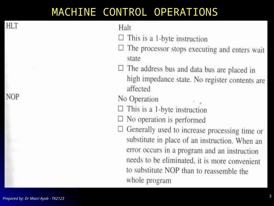
MACHINE CONTROL OPERATIONSMACHINE CONTROL OPERATIONS
Prepared by: Dr Masri AyobPrepared by: Dr Masri Ayob - TK2123 - TK212344
DATA TRANSFER OPERATIONSDATA TRANSFER OPERATIONS
The data transfer instructions The data transfer instructions ‘copy’‘copy’ data data from a source into a destination without from a source into a destination without modifying the contents of the source. modifying the contents of the source.
The previous contents of the destination are The previous contents of the destination are replaced by the contents of the source. replaced by the contents of the source.

Prepared by: Dr Masri AyobPrepared by: Dr Masri Ayob - TK2123 - TK212355
DATA TRANSFER OPERATIONSDATA TRANSFER OPERATIONS
Prepared by: Dr Masri AyobPrepared by: Dr Masri Ayob - TK2123 - TK212366
Prepared by: Dr Masri AyobPrepared by: Dr Masri Ayob - TK2123 - TK212377
Prepared by: Dr Masri AyobPrepared by: Dr Masri Ayob - TK2123 - TK212388
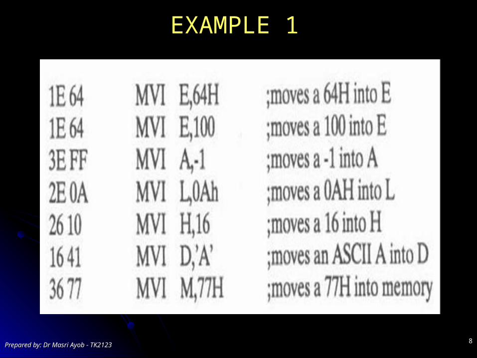
EXAMPLE 1EXAMPLE 1
Prepared by: Dr Masri AyobPrepared by: Dr Masri Ayob - TK2123 - TK212399
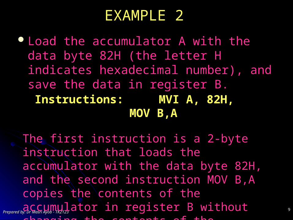
EXAMPLE 2EXAMPLE 2
Load the accumulator A with the data byte Load the accumulator A with the data byte 82H (the letter H indicates hexadecimal 82H (the letter H indicates hexadecimal number), and save the data in register B.number), and save the data in register B.
Instructions:Instructions: MVI A, 82H, MVI A, 82H, MOV B,AMOV B,A
The first instruction is a 2-byte instruction that loads the accumulator with the data byte 82H, and the second instruction MOV B,A copies the contents of the accumulator in register B without changing the contents of the accumulator.

Prepared by: Dr Masri AyobPrepared by: Dr Masri Ayob - TK2123 - TK21231010
EXAMPLE 3EXAMPLE 3 Write instructions to read 8 ON/OFF switches connected to the input Write instructions to read 8 ON/OFF switches connected to the input
port with the address OOH, and turn on the devices connected to the port with the address OOH, and turn on the devices connected to the output port with the address 01H, as shown in Figure 6.1. output port with the address 01H, as shown in Figure 6.1.

Prepared by: Dr Masri AyobPrepared by: Dr Masri Ayob - TK2123 - TK21231111
SOLUTION FOR EXAMPLE 3SOLUTION FOR EXAMPLE 3
The input has eight switches that are connected to the data bus through The input has eight switches that are connected to the data bus through the tri-state buffer. the tri-state buffer. Any one of the switches can be connected to +5 V (logic 1) or to ground Any one of the switches can be connected to +5 V (logic 1) or to ground
(logic 0), (logic 0), and each switch controls the corresponding device at the output port. and each switch controls the corresponding device at the output port. The microprocessor needs to read the bit pattern on the switches and send The microprocessor needs to read the bit pattern on the switches and send
the same bit pattern to the output port to turn on the corresponding devices. the same bit pattern to the output port to turn on the corresponding devices.
Instructions:Instructions: IN IN OOHOOH OUTOUT 01H01H
HLTHLT
When MPU executes the instruction IN 00H, it enables the tri-state buffer. When MPU executes the instruction IN 00H, it enables the tri-state buffer. The bit pattern 4FH formed by the switch positions is placed on the data bus and The bit pattern 4FH formed by the switch positions is placed on the data bus and
transferred to the accumulator (reading an input port).transferred to the accumulator (reading an input port). When MPU executes OUT 01H, When MPU executes OUT 01H,
it places the contents of the accumulator on the data bus and enables the output port it places the contents of the accumulator on the data bus and enables the output port O1H (writing to output port).O1H (writing to output port).
The output port latches the bit pattern and turns ON/OFF the devices connected to the The output port latches the bit pattern and turns ON/OFF the devices connected to the port according to the bit pattern. port according to the bit pattern.

Prepared by: Dr Masri AyobPrepared by: Dr Masri Ayob - TK2123 - TK21231212
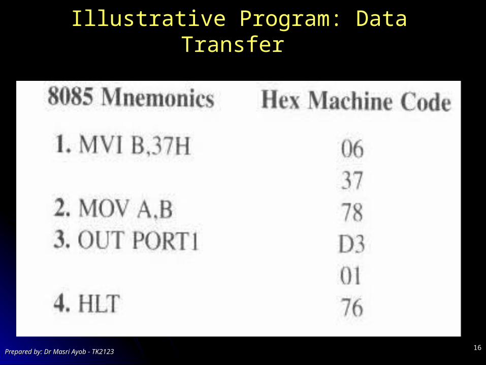
Illustrative Program: Data Transfer Illustrative Program: Data Transfer
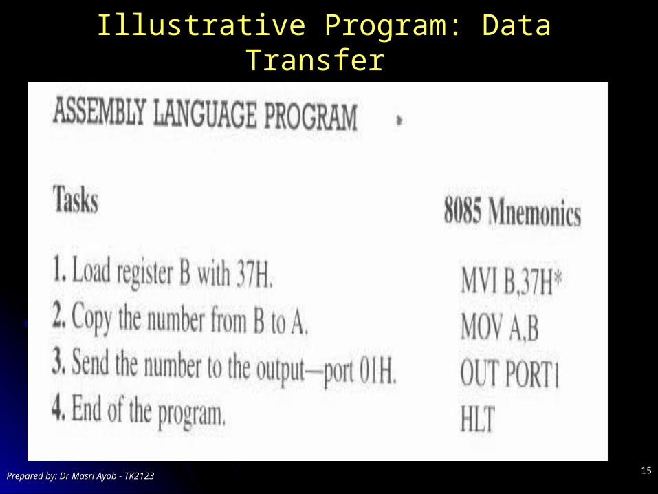
PROBLEM STATEMENTPROBLEM STATEMENT Load the hexadecimal number 37H in register B, and Load the hexadecimal number 37H in register B, and
display the number at the output port labeled PORT1.display the number at the output port labeled PORT1.
PROBLEM ANALYSISPROBLEM ANALYSIS Step 1: Load register B with a number.Step 1: Load register B with a number. Step 2: Send the number to the output port.Step 2: Send the number to the output port.
QUESTIONS TO BE ASKEDQUESTIONS TO BE ASKED Is there an instruction to load the register B? YES—MVI B.Is there an instruction to load the register B? YES—MVI B. Is there an instruction to send the data from register B to the output port? Is there an instruction to send the data from register B to the output port?
NO. Review the instruction OUT. This instruction sends data from the NO. Review the instruction OUT. This instruction sends data from the accumulator to an output port.accumulator to an output port.
The solution appears to be as follows: Copy the number from register B into The solution appears to be as follows: Copy the number from register B into accumulator A.accumulator A.
Is there an instruction to copy data from one register to another register? Is there an instruction to copy data from one register to another register? YES—MOV Rd,Rs.YES—MOV Rd,Rs.

Prepared by: Dr Masri AyobPrepared by: Dr Masri Ayob - TK2123 - TK21231313
Illustrative Program: Data Transfer Illustrative Program: Data Transfer FLOWCHART FLOWCHART
Generally, a flowchart is used for two purposes:Generally, a flowchart is used for two purposes: to assist and clarify the thinking process to assist and clarify the thinking process and to communicate the programmer’s thoughts or logic to others. and to communicate the programmer’s thoughts or logic to others.

Prepared by: Dr Masri AyobPrepared by: Dr Masri Ayob - TK2123 - TK21231414
Illustrative Program: Data Transfer Illustrative Program: Data Transfer
Prepared by: Dr Masri AyobPrepared by: Dr Masri Ayob - TK2123 - TK21231515
Illustrative Program: Data Transfer Illustrative Program: Data Transfer
Prepared by: Dr Masri AyobPrepared by: Dr Masri Ayob - TK2123 - TK21231616
Illustrative Program: Data Transfer Illustrative Program: Data Transfer
Prepared by: Dr Masri AyobPrepared by: Dr Masri Ayob - TK2123 - TK21231717
Exercises Exercises
Write instructions to read the data at input Write instructions to read the data at input PORT 07H and at PORT 08H. Display the PORT 07H and at PORT 08H. Display the input data from PORT 07H at output PORT input data from PORT 07H at output PORT OOH, and store the input data from PORT OOH, and store the input data from PORT 08H in register B.08H in register B.
Prepared by: Dr Masri AyobPrepared by: Dr Masri Ayob - TK2123 - TK21231818
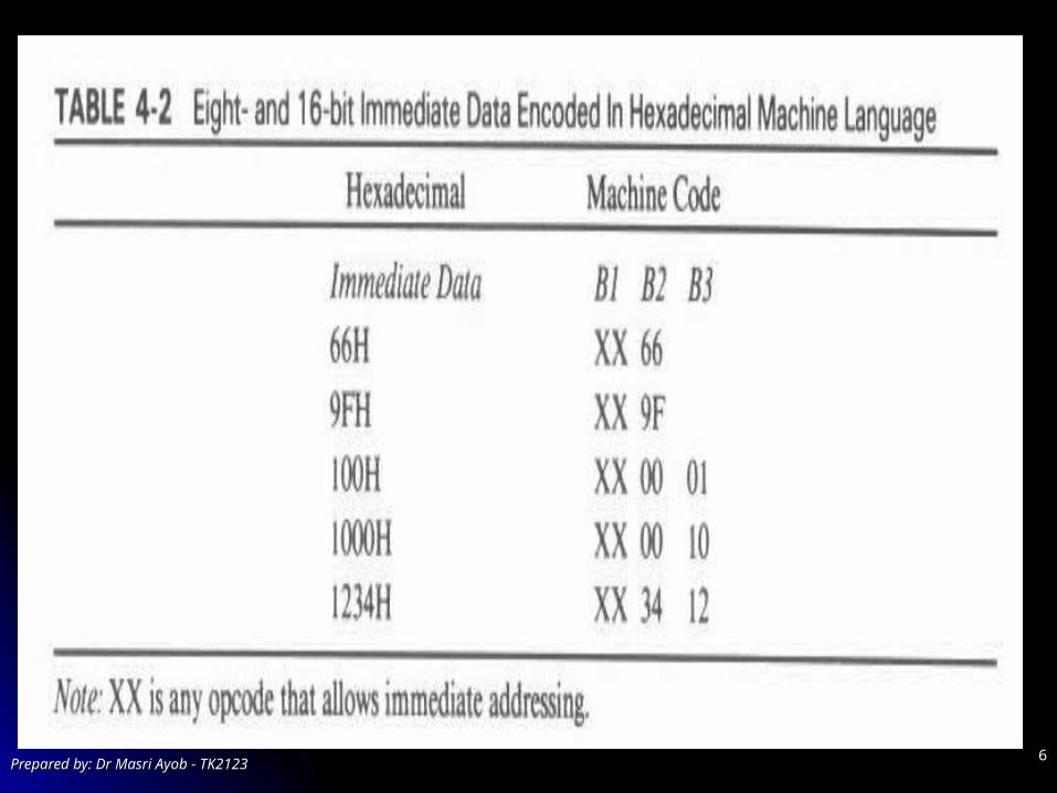
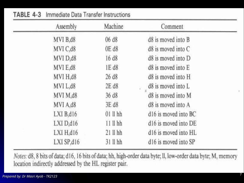
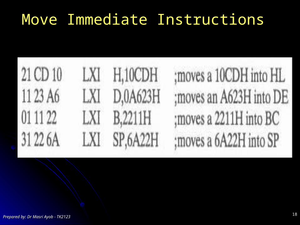
Move Immediate Instructions Move Immediate Instructions

Prepared by: Dr Masri AyobPrepared by: Dr Masri Ayob - TK2123 - TK21231919
Move Immediate Instructions Move Immediate Instructions
The memory location, which is indirectly addressed by the HL register pair, appears as the letter M in all instructions.

Prepared by: Dr Masri AyobPrepared by: Dr Masri Ayob - TK2123 - TK21232020
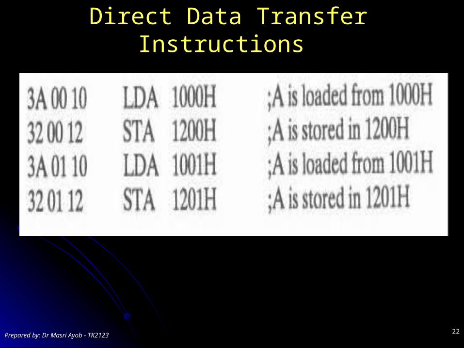
Direct Data Transfer Instructions Direct Data Transfer Instructions
Direct data transfer instructions are useful Direct data transfer instructions are useful if only one byte or word of data is if only one byte or word of data is transferred to or from the memory. transferred to or from the memory.
If more than one byte or word is If more than one byte or word is transferred, it is more efficient to use transferred, it is more efficient to use indirectly addressed instruction. indirectly addressed instruction.

Prepared by: Dr Masri AyobPrepared by: Dr Masri Ayob - TK2123 - TK21232121
Direct Data Transfer Instructions Direct Data Transfer Instructions
Prepared by: Dr Masri AyobPrepared by: Dr Masri Ayob - TK2123 - TK21232222
Direct Data Transfer Instructions Direct Data Transfer Instructions
Prepared by: Dr Masri AyobPrepared by: Dr Masri Ayob - TK2123 - TK21232323
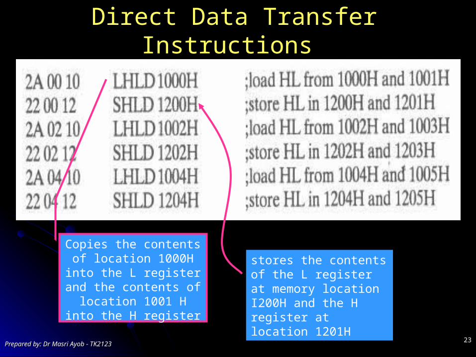
Direct Data Transfer Instructions Direct Data Transfer Instructions
Copies the contents of location 1000H into the L register and the contents of location 1001 H into
the H register
stores the contents of the L register at memory location I200H and the H register at location 1201H

Prepared by: Dr Masri AyobPrepared by: Dr Masri Ayob - TK2123 - TK21232424
INDIRECT DATA TRANSFER INDIRECT DATA TRANSFER INSTRUCTIONS INSTRUCTIONS
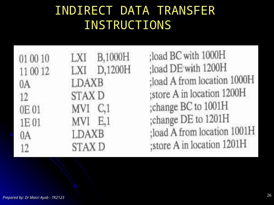
With register indirect addressing, a register With register indirect addressing, a register pair holds the address of the memory pair holds the address of the memory location accessed by the instruction.location accessed by the instruction.
The contents of the register pair indirectly The contents of the register pair indirectly addresses a memory location.addresses a memory location.
Whenever, the letter M appears instead of a Whenever, the letter M appears instead of a register, the HL register pair indirectly register, the HL register pair indirectly addresses a memory location.addresses a memory location.

Prepared by: Dr Masri AyobPrepared by: Dr Masri Ayob - TK2123 - TK21232525
INDIRECT DATA TRANSFER INDIRECT DATA TRANSFER INSTRUCTIONS INSTRUCTIONS
Prepared by: Dr Masri AyobPrepared by: Dr Masri Ayob - TK2123 - TK21232626
INDIRECT DATA TRANSFER INDIRECT DATA TRANSFER INSTRUCTIONS INSTRUCTIONS
Prepared by: Dr Masri AyobPrepared by: Dr Masri Ayob - TK2123 - TK21232727
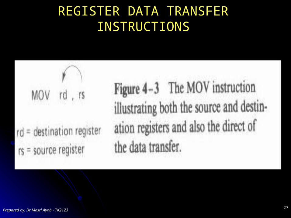
REGISTER DATA TRANSFER REGISTER DATA TRANSFER INSTRUCTIONSINSTRUCTIONS

Prepared by: Dr Masri AyobPrepared by: Dr Masri Ayob - TK2123 - TK21232828
REGISTER DATA TRANSFER REGISTER DATA TRANSFER INSTRUCTIONSINSTRUCTIONS

Prepared by: Dr Masri AyobPrepared by: Dr Masri Ayob - TK2123 - TK21232929
STACK DATA TRANSFER INSTRUCTIONSSTACK DATA TRANSFER INSTRUCTIONS
The Intel 8085A microprocessor has a LIFO (last-The Intel 8085A microprocessor has a LIFO (last-in, first-out) stack memory.in, first-out) stack memory.
The stack memory stores both return addresses The stack memory stores both return addresses from subroutines and data temporarily.from subroutines and data temporarily.
The microprocessor cannot locate the stack The microprocessor cannot locate the stack memory when power is first applied to the system memory when power is first applied to the system because the number in the SP is unknown.because the number in the SP is unknown.
The location of the stack must be initialised after The location of the stack must be initialised after the application of system power. the application of system power.
Prepared by: Dr Masri AyobPrepared by: Dr Masri Ayob - TK2123 - TK21233030
STACK DATA TRANSFER INSTRUCTIONSSTACK DATA TRANSFER INSTRUCTIONS
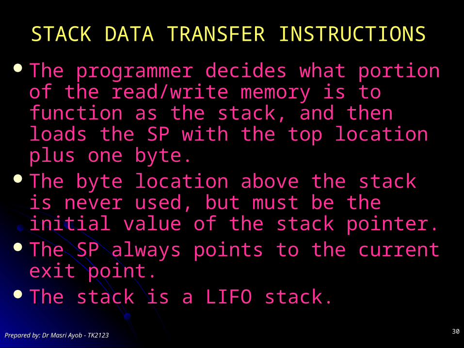
The programmer decides what portion of the The programmer decides what portion of the read/write memory is to function as the stack, read/write memory is to function as the stack, and then loads the SP with the top location and then loads the SP with the top location plus one byte. plus one byte.
The byte location above the stack is never The byte location above the stack is never used, but must be the initial value of the used, but must be the initial value of the stack pointer. stack pointer.
The SP always points to the current exit The SP always points to the current exit point. point.
The stack is a LIFO stack.The stack is a LIFO stack.

Prepared by: Dr Masri AyobPrepared by: Dr Masri Ayob - TK2123 - TK21233131
STACK DATA TRANSFER INSTRUCTIONSSTACK DATA TRANSFER INSTRUCTIONS
If data are pushed (placed) onto the stack, they If data are pushed (placed) onto the stack, they move into the memory locations addressed by SP-1 move into the memory locations addressed by SP-1 and SP-2.and SP-2. Note that pairs of registers always move to the stack.Note that pairs of registers always move to the stack. A PUSH instruction stores the high-order register first A PUSH instruction stores the high-order register first
(SP - 1), followed by the low-order register (SP -2). (SP - 1), followed by the low-order register (SP -2). The SP then decrements by two so that the next push The SP then decrements by two so that the next push
occurs below the first.occurs below the first. Notice that when the PUSH occurs, nothing is placed at Notice that when the PUSH occurs, nothing is placed at
the location addressed by the stack pointer. the location addressed by the stack pointer. This is why the SP is initialised at one byte above the top This is why the SP is initialised at one byte above the top
of the stack. of the stack.
Prepared by: Dr Masri AyobPrepared by: Dr Masri Ayob - TK2123 - TK21233232
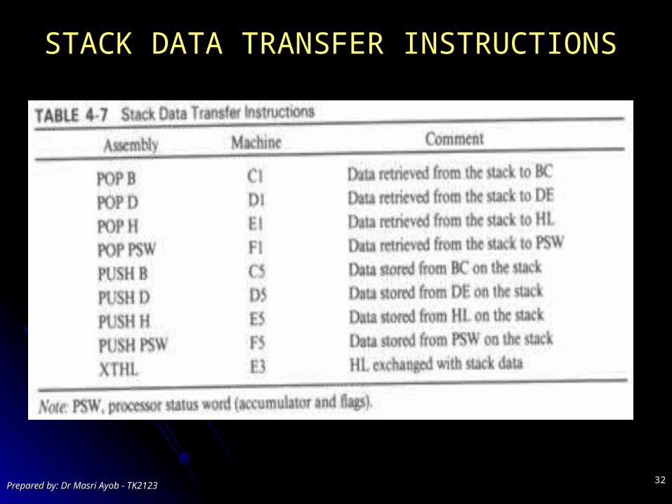
STACK DATA TRANSFER INSTRUCTIONSSTACK DATA TRANSFER INSTRUCTIONS

Prepared by: Dr Masri AyobPrepared by: Dr Masri Ayob - TK2123 - TK21233333
STACK DATA TRANSFER INSTRUCTIONSSTACK DATA TRANSFER INSTRUCTIONS
Prepared by: Dr Masri AyobPrepared by: Dr Masri Ayob - TK2123 - TK21233434
STACK DATA TRANSFER INSTRUCTIONS STACK DATA TRANSFER INSTRUCTIONS
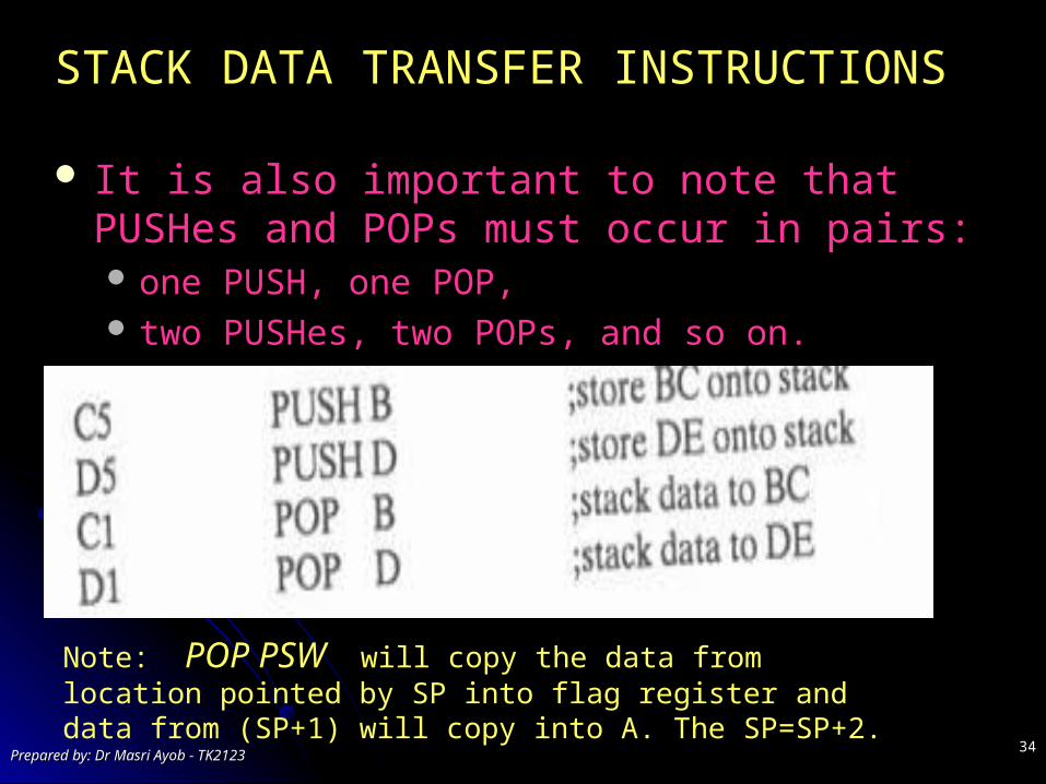
It is also important to note that PUSHes and It is also important to note that PUSHes and POPs must occur in pairs: POPs must occur in pairs: one PUSH, one POP, one PUSH, one POP, two PUSHes, two POPs, and so on. two PUSHes, two POPs, and so on.
Note: POP PSW will copy the data from location pointed by SP into flag register and data from (SP+1) will copy into A. The SP=SP+2.

Prepared by: Dr Masri AyobPrepared by: Dr Masri Ayob - TK2123 - TK21233535
MISCELLANEOUS DATA TRANSFER MISCELLANEOUS DATA TRANSFER INSTRUQTIONS INSTRUQTIONS
Exchange DE with HL (XCHG)Exchange DE with HL (XCHG) The XCHG instruction exchanges the contents of the HL register The XCHG instruction exchanges the contents of the HL register
pair with the contents of the DE register pair. pair with the contents of the DE register pair.
Load SP from HL (SPHL)Load SP from HL (SPHL) Is a one-byte instruction, copies the contents of the HL register Is a one-byte instruction, copies the contents of the HL register
pair into the SP.pair into the SP.
Exchange HL with Stack Data (XTHL)Exchange HL with Stack Data (XTHL) This instruction exchanges the contents of the HL pair with the This instruction exchanges the contents of the HL pair with the
most recent data on the stack.most recent data on the stack. Input/Output Data Transfer Instructions Input/Output Data Transfer Instructions
IN : IN : instruction inputs data from an I/O device into the accumulator. instruction inputs data from an I/O device into the accumulator. OUT : OUT : sends accumulator data out to an I/O device.sends accumulator data out to an I/O device.

Prepared by: Dr Masri AyobPrepared by: Dr Masri Ayob - TK2123 - TK21233636
SUMMARY SUMMARY
Data transfer instructions transfer information from register to register, Data transfer instructions transfer information from register to register, from register to memory, from memory to register. from register to memory, from memory to register.
Data transfer instructions also allow data transfer between registers Data transfer instructions also allow data transfer between registers and stack or the I/O devices in a system.and stack or the I/O devices in a system.
The Intel 8085A uses four different addressing modes: direct, register, The Intel 8085A uses four different addressing modes: direct, register, register indirect, and immediate.register indirect, and immediate.
Direct addressing accesses a memory location to transfer data Direct addressing accesses a memory location to transfer data between memory and the accumulator or HL register pair. The between memory and the accumulator or HL register pair. The address of the data follow with the instruction in the memory.address of the data follow with the instruction in the memory.
Register addressing allows either a single 8-bit register (B, C, D, E, H, Register addressing allows either a single 8-bit register (B, C, D, E, H, L, or A) or a 16-bit register pair (BC, DE, HL, and SP).L, or A) or a 16-bit register pair (BC, DE, HL, and SP).
Register indirect addressing allows the instruction to address memory Register indirect addressing allows the instruction to address memory
through the address held in a register pair.through the address held in a register pair.

Prepared by: Dr Masri AyobPrepared by: Dr Masri Ayob - TK2123 - TK21233737
SUMMARY SUMMARY
Immediate addressing is used whenever the data (8 or 16 Immediate addressing is used whenever the data (8 or 16 bits) are a constant. Immediate data immediately follow the bits) are a constant. Immediate data immediately follow the opcode in the program.opcode in the program.
The M register or operand indirectly addresses memory The M register or operand indirectly addresses memory through the HL register pair.through the HL register pair.
The LDA and STA instructions load or store the The LDA and STA instructions load or store the accumulator. The LHLD and SHLD instructions load or store accumulator. The LHLD and SHLD instructions load or store the HL register pair.the HL register pair.
Besides M for indirectly addressing the memory, the DE and Besides M for indirectly addressing the memory, the DE and BC register pairs are also available. The LDAX and STAX BC register pairs are also available. The LDAX and STAX instructions allow the accumulator to be indirectly stored or instructions allow the accumulator to be indirectly stored or loaded from the memory by using the BC or DE register loaded from the memory by using the BC or DE register pairs. pairs.
Prepared by: Dr Masri AyobPrepared by: Dr Masri Ayob - TK2123 - TK21233838
SUMMARY SUMMARY
Register data transfer instructions are the most numerous form of data Register data transfer instructions are the most numerous form of data transfer: 63 instructions.transfer: 63 instructions.
The stack memory is a LIFO (last-in, first-out) memory that stores data The stack memory is a LIFO (last-in, first-out) memory that stores data and return addresses from subroutines.and return addresses from subroutines.
The SP register indirectly addresses the stack. The stack functions The SP register indirectly addresses the stack. The stack functions with the stack data transfer instructions PUSH, POP, and XTHL.with the stack data transfer instructions PUSH, POP, and XTHL.
The PSW is the processor status word that contains both the The PSW is the processor status word that contains both the accumulator and the flag byte. The accumulator is the high-order accumulator and the flag byte. The accumulator is the high-order register and the flag bits are the low-order register.register and the flag bits are the low-order register.
IN and OUT effect data transfers between an external I/O device and IN and OUT effect data transfers between an external I/O device and the accumulator. the accumulator.
I/O devices are often called I/O ports and are addressed by an 8-bit I/O devices are often called I/O ports and are addressed by an 8-bit I/O port address. I/O port address.

Prepared by: Dr Masri AyobPrepared by: Dr Masri Ayob - TK2123 - TK21233939
ExercisesExercises
Write a sequence of immediate instructions that store a Write a sequence of immediate instructions that store a 16H into memory location 1200H and a 17H in memory 16H into memory location 1200H and a 17H in memory location 1202H. location 1202H.
Write a sequence of instructions that use register indirect Write a sequence of instructions that use register indirect addressing to transfer the contents of A into location addressing to transfer the contents of A into location 2800H, B into 2801H, and C into 2802H. 2800H, B into 2801H, and C into 2802H.
Write a sequence of instructions that use register indirect Write a sequence of instructions that use register indirect addressing to transfer the number stored in memory addressing to transfer the number stored in memory location 1300H into memory location 2302H. location 1300H into memory location 2302H.

Prepared by: Dr Masri AyobPrepared by: Dr Masri Ayob - TK2123 - TK21234040
Thank youThank youQ&AQ&A
Related Documents