RM42 Hercules Development Kit (HDK) User's Guide Literature Number: SPNU567 September 2012

Welcome message from author
This document is posted to help you gain knowledge. Please leave a comment to let me know what you think about it! Share it to your friends and learn new things together.
Transcript
RM42 Hercules Development Kit (HDK)
User's Guide
Literature Number: SPNU567
September 2012
Contents
Preface ....................................................................................................................................... 4
1 Introduction ........................................................................................................................ 51.1 Scope of Document ......................................................................................................... 51.2 RM42 HERCULES Development Kit (HDK) Features ................................................................. 51.3 HDK Board Block Diagram ................................................................................................ 61.4 RM42 HDK Contents ....................................................................................................... 61.5 HDK Specifications ......................................................................................................... 71.6 Basic Operation ............................................................................................................. 71.7 Memory Map ................................................................................................................. 71.8 Power Supply ................................................................................................................ 7
2 Physical Description ............................................................................................................ 82.1 Board Layout ................................................................................................................ 82.2 Connectors ................................................................................................................... 9
2.2.1 20-Pin ARM JTAG Header ........................................................................................ 92.2.2 20-Pin Compact TI JTAG Header .............................................................................. 102.2.3 CAN Interface ..................................................................................................... 102.2.4 J4, XDS100V2 USB JTAG Interface ........................................................................... 112.2.5 P1, +5 V to +12 V Input .......................................................................................... 112.2.6 Virtual COM Port Interface ...................................................................................... 122.2.7 Daughter Card Interface ......................................................................................... 12
2.3 LEDs ........................................................................................................................ 162.4 Emulator and Pin Multiplexing Selection DIP Switch ................................................................. 162.5 Jumpers ..................................................................................................................... 172.6 S3, Power-On Reset Switch ............................................................................................. 172.7 S2, System Reset Switch ................................................................................................ 172.8 S4, Pushbutton for Clock Failure Test .................................................................................. 17
A Operation Notices .............................................................................................................. 18A.1 Support Resources ........................................................................................................ 18
2 Contents SPNU567–September 2012Submit Documentation Feedback
Copyright © 2012, Texas Instruments Incorporated
www.ti.com
List of Figures
1-1. RM42 HDK Board Block Diagram ........................................................................................ 6
2-1. RM42 HDK Board........................................................................................................... 8
2-2. Connectors on RM42 HDK Table......................................................................................... 9
2-3. CAN Bus Termination..................................................................................................... 11
2-4. J1, J2 Screw Terminal Block for CAN Bus............................................................................. 11
2-5. +12 V Input Jack........................................................................................................... 12
2-6. J9, J10 and J11 Connectors ............................................................................................. 13
2-7. DIP Switch Settings ....................................................................................................... 16
List of Tables
1-1. RM42L432 Memory Map................................................................................................... 7
1-2. Power Supply Selection .................................................................................................... 7
1-3. Power Test Points .......................................................................................................... 7
2-1. Connectors on HDK Board ................................................................................................ 9
2-2. 20-Pin ARM JTAG Header ............................................................................................... 10
2-3. 20-Pin CTI JTAG Header................................................................................................. 10
2-4. Expansion Connector P2 (J9, Right, TopView)........................................................................ 13
2-5. Expansion Connector P1 (J9, Left, TopView) ......................................................................... 14
2-6. Expansion Connector P3 (J11, Bottom One, TopView) .............................................................. 15
2-7. Demo LEDs ................................................................................................................ 16
2-8. Other LEDs as Indicator .................................................................................................. 16
2-9. S5 DIP Switch Functions ................................................................................................. 16
2-10. Jumpers..................................................................................................................... 17
3SPNU567–September 2012 List of FiguresSubmit Documentation Feedback
Copyright © 2012, Texas Instruments Incorporated
PrefaceSPNU567–September 2012
Read This First
About This Manual
This document describes the board level operations of the RM42 Hercules™ Development Kit (HDK). TheHDK is based on the Texas Instruments RM42L432 Microcontroller. The RM42 HDK is a table top cardthat allows engineers and software developers to evaluate certain characteristics of the RM42L432microcontroller to determine if the microcontroller meets the designer application requirements. Evaluatorscan create software to execute on board or expand the system in a variety of ways.
Notational Conventions
This document uses the following conventions.
The RM42 HDK will sometimes be referred to as the HDK.
Program listings, program examples, and interactive displays are shown in a special italic typeface. Hereis a sample program listing:
• equations
• !rd = !strobe&rw;
Information About Cautions
This book may contain cautions.
This is an example of a caution statement.
A caution statement describes a situation that could potentially damage your software, or hardware, orother equipment. The information in a caution is provided for your protection. Please read each cautioncarefully.
Related Documentation From Texas Instruments
Information regarding this device can be found at the following Texas Instruments website:http://www.ti.com/rm4
4 Read This First SPNU567–September 2012Submit Documentation Feedback
Copyright © 2012, Texas Instruments Incorporated
Chapter 1SPNU567–September 2012
Introduction
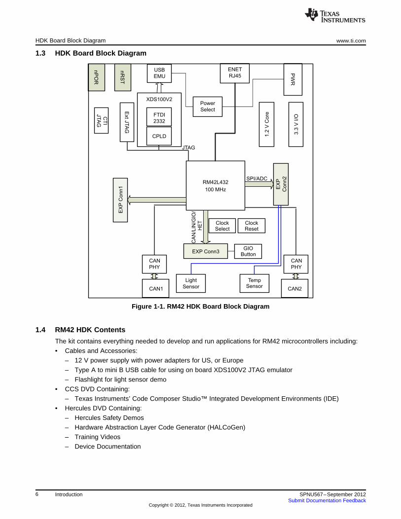
The RM42L432 HDK is a low cost and easy to use hardware and software platform for evaluating thefunctionality of the Texas Instruments RM42L432 microcontroller family. Project collateral, schematics andPCB layouts discussed in this application report can be downloaded from the following URL:
(http://processors.wiki.ti.com/index.php/RM42_HDK_Kit).
1.1 Scope of Document
This user guide will list the contents of the development kit, point out the features of the majorcomponents, and provide the instructions necessary to verify your development kit is in working order. Anyadditional usage instructions or details fall outside the scope of this document. Additional resources arelisted at the end of this user guide.
1.2 RM42 HERCULES Development Kit (HDK) Features
The HDK comes with a full complement of on board devices that suit a wide variety of applicationenvironments. Key features include:
• A Hercules RM42L432 100-pin QFP microcontroller
• Integrated USB JTAG emulator (XDS100v2)
• External JTAG headers ( ARM® 20 pin and TI compact 20-pin CTI)
• One DIP switch to select pull-up or pull-down for JTAG nTRST
• Two CAN transceivers (SN65HVDA541Q1) and screw terminal blocks
• One ambient light sensor
• One ambient temperature sensor
• Microcontroller’s serial communications interface (SCI) universal asynchronous receiver/transmitter(UART) accessible through a USB virtual COM port
• Four user programmable white LEDs
• One user programmable pushbutton
• Three expansion connectors for hardware prototyping
• Reset and power-on reset pushbuttons (nRST and nPORRST)
• One pushbutton simulating external oscillator failure
• One Jumper to select clock source for MCU: crystal or crystal oscillator
• One crystal socket (HC-18)
• One SD card slot (SPI mode)
• Current measurement capability for 3.3 V IO, 3.3 V analog-to digital converter (ADC) and, 1.2 V corevoltage
• May be powered by USB or an external power supply in case additional power is required (forexpansion boards)
• Accepts an external power supply between +5 V and +12 V
5SPNU567–September 2012 IntroductionSubmit Documentation Feedback
Copyright © 2012, Texas Instruments Incorporated
RM42L432
100 MHz
Power
Select
GIOButton
Light
Sensor
ENET
RJ45
XDS100V2
FTDI
2332
CPLD
USB
EMU
CAN
PHY
CAN
PHY
CAN1 CAN2
TempSensor
Ext J
TA
G
1.2
V C
ore
3.3
V I/O
PW
R
EX
PC
onn1
EXP Conn3
EX
P
Conn2
nP
OR
nR
ST
SPI/ADC
JTAG
CA
N/L
IN/G
IO/
HE
T
CT
I
JTA
G
ClockReset
ClockSelect
HDK Board Block Diagram www.ti.com
1.3 HDK Board Block Diagram
Figure 1-1. RM42 HDK Board Block Diagram
1.4 RM42 HDK Contents
The kit contains everything needed to develop and run applications for RM42 microcontrollers including:
• Cables and Accessories:
– 12 V power supply with power adapters for US, or Europe
– Type A to mini B USB cable for using on board XDS100V2 JTAG emulator
– Flashlight for light sensor demo
• CCS DVD Containing:
– Texas Instruments’ Code Composer Studio™ Integrated Development Environments (IDE)
• Hercules DVD Containing:
– Hercules Safety Demos
– Hardware Abstraction Layer Code Generator (HALCoGen)
– Training Videos
– Device Documentation
6 Introduction SPNU567–September 2012Submit Documentation Feedback
Copyright © 2012, Texas Instruments Incorporated
www.ti.com HDK Specifications
1.5 HDK Specifications• Board supply voltage: 5 V to 12 V DC
• Board supply current: 130 mA typ (fully active, CPU at 100 MHz)
• Dimensions: 4.90” x 4.30” x 0.85” (LxWxH)
1.6 Basic Operation
The HDK is designed to work with TI’s Code Composer Studio and other third party ARM IDEs. The IDEscommunicate with the board through the embedded emulator or an external JTAG emulator. To getstarted, follow the instructions in the Quick Start Guide to install Hercules specific software. This processwill install all of the necessary development tools, documentation, and drivers.
1.7 Memory Map
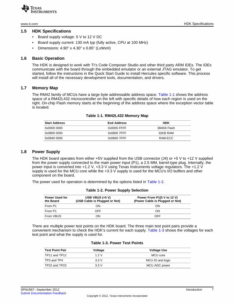
The RM42 family of MCUs have a large byte addressable address space. Table 1-1 shows the addressspace of a RM42L432 microcontroller on the left with specific details of how each region is used on theright. On-chip Flash memory starts at the beginning of the address space where the exception vector tableis located.
Table 1-1. RM42L432 Memory Map
Start Address End Address HDK
0x0000 0000 0x0005 FFFF 384KB Flash
0x0800 0000 0x0800 7FFF 32KB RAM
0x0840 0000 0x0840 7FFF RAM-ECC
1.8 Power Supply
The HDK board operates from either +5V supplied from the USB connector (J4) or +5 V to +12 V suppliedfrom the power supply connected to the main power input (P1), a 2.5 MM, barrel-type plug. Internally, thepower input is converted into +1.2 V, +3.3 V using Texas Instruments voltage regulators. The +1.2 Vsupply is used for the MCU core while the +3.3 V supply is used for the MCU's I/O buffers and othercomponent on the board.
The power used for operation is determined by the options listed in Table 1-2.
Table 1-2. Power Supply Selection
Power Used for USB VBUS (+5 V) Power From P1(5 V to 12 V)the Board (USB Cable is Plugged or Not) (Power Cable is Plugged or Not)
From P1 ON ON
From P1 OFF ON
From VBUS ON OFF
There are multiple power test points on the HDK board. The three main test point pairs provide aconvenient mechanism to check the HDK’s current for each supply. Table 1-3 shows the voltages for eachtest point and what the supply is used for.
Table 1-3. Power Test Points
Test Point Pair Voltage Voltage Use
TP11 and TP12 1.2 V MCU core
TP3 and TP4 3.3 V MCU IO and logic
TP22 and TP23 3.3 V MCU ADC power
7SPNU567–September 2012 IntroductionSubmit Documentation Feedback
Copyright © 2012, Texas Instruments Incorporated
RM42L432
Chapter 2SPNU567–September 2012
Physical Description
This chapter describes the physical layout of the RM42 HDK board and its interfaces.
2.1 Board Layout
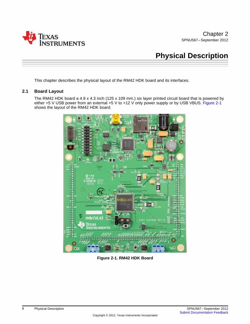
The RM42 HDK board a 4.9 x 4.3 inch (125 x 109 mm.) six layer printed circuit board that is powered byeither +5 V USB power from an external +5 V to +12 V only power supply or by USB VBUS. Figure 2-1shows the layout of the RM42 HDK board.
Figure 2-1. RM42 HDK Board
8 Physical Description SPNU567–September 2012Submit Documentation Feedback
Copyright © 2012, Texas Instruments Incorporated
J15
J3
J10 J9
J11
J5
J1 J2
J4P1
RM42L432
www.ti.com Connectors
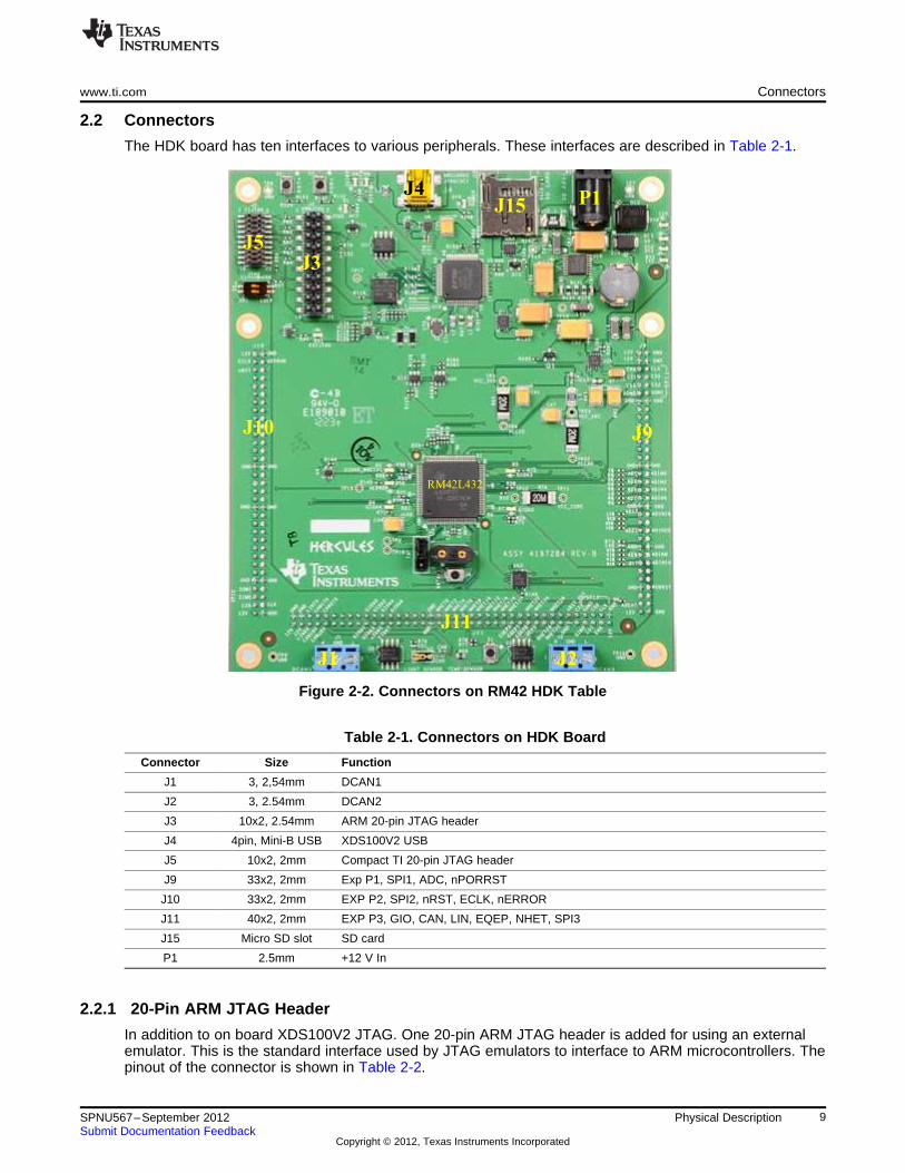
2.2 Connectors
The HDK board has ten interfaces to various peripherals. These interfaces are described in Table 2-1.
Figure 2-2. Connectors on RM42 HDK Table
Table 2-1. Connectors on HDK Board
Connector Size Function
J1 3, 2,54mm DCAN1
J2 3, 2.54mm DCAN2
J3 10x2, 2.54mm ARM 20-pin JTAG header
J4 4pin, Mini-B USB XDS100V2 USB
J5 10x2, 2mm Compact TI 20-pin JTAG header
J9 33x2, 2mm Exp P1, SPI1, ADC, nPORRST
J10 33x2, 2mm EXP P2, SPI2, nRST, ECLK, nERROR
J11 40x2, 2mm EXP P3, GIO, CAN, LIN, EQEP, NHET, SPI3
J15 Micro SD slot SD card
P1 2.5mm +12 V In
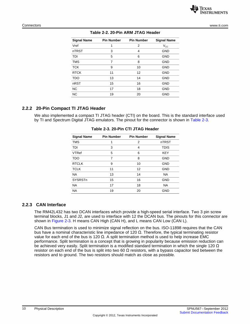
2.2.1 20-Pin ARM JTAG Header
In addition to on board XDS100V2 JTAG. One 20-pin ARM JTAG header is added for using an externalemulator. This is the standard interface used by JTAG emulators to interface to ARM microcontrollers. Thepinout of the connector is shown in Table 2-2.
9SPNU567–September 2012 Physical DescriptionSubmit Documentation Feedback
Copyright © 2012, Texas Instruments Incorporated
Connectors www.ti.com
Table 2-2. 20-Pin ARM JTAG Header
Signal Name Pin Number Pin Number Signal Name
Vref 1 2 VCC
nTRST 3 4 GND
TDI 5 6 GND
TMS 7 8 GND
TCK 9 10 GND
RTCK 11 12 GND
TDO 13 14 GND
nRST 15 16 GND
NC 17 18 GND
NC 19 20 GND
2.2.2 20-Pin Compact TI JTAG Header
We also implemented a compact TI JTAG header (CTI) on the board. This is the standard interface usedby TI and Spectrum Digital JTAG emulators. The pinout for the connector is shown in Table 2-3.
Table 2-3. 20-Pin CTI JTAG Header
Signal Name Pin Number Pin Number Signal Name
TMS 1 2 nTRST
TDI 3 4 TDIS
VTRef 5 6 KEY
TDO 7 8 GND
RTCLK 9 10 GND
TCLK 11 12 GND
NA 13 14 NA
SYSRSTn 15 16 GND
NA 17 18 NA
NA 19 20 GND
2.2.3 CAN Interface
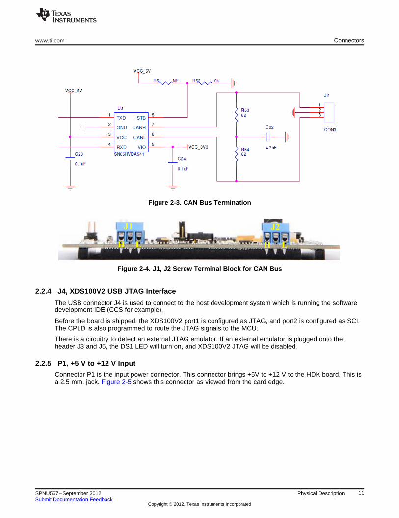
The RM42L432 has two DCAN interfaces which provide a high-speed serial interface. Two 3 pin screwterminal blocks, J1 and J2, are used to interface with 12 the DCAN bus. The pinouts for this connector areshown in Figure 2-3. H means CAN High (CAN H), and L means CAN Low (CAN L).
CAN Bus termination is used to minimize signal reflection on the bus. ISO-11898 requires that the CANbus have a nominal characteristic line impedance of 120 Ω. Therefore, the typical terminating resistorvalue for each end of the bus is 120 Ω. A split termination method is used to help increase EMCperformance. Split termination is a concept that is growing in popularity because emission reduction canbe achieved very easily. Split termination is a modified standard termination in which the single 120 Ωresistor on each end of the bus is split into two 60 Ω resistors, with a bypass capacitor tied between theresistors and to ground. The two resistors should match as close as possible.
10 Physical Description SPNU567–September 2012Submit Documentation Feedback
Copyright © 2012, Texas Instruments Incorporated
J1 J2
H HL L
www.ti.com Connectors
Figure 2-3. CAN Bus Termination
Figure 2-4. J1, J2 Screw Terminal Block for CAN Bus
2.2.4 J4, XDS100V2 USB JTAG Interface
The USB connector J4 is used to connect to the host development system which is running the softwaredevelopment IDE (CCS for example).
Before the board is shipped, the XDS100V2 port1 is configured as JTAG, and port2 is configured as SCI.The CPLD is also programmed to route the JTAG signals to the MCU.
There is a circuitry to detect an external JTAG emulator. If an external emulator is plugged onto theheader J3 and J5, the DS1 LED will turn on, and XDS100V2 JTAG will be disabled.
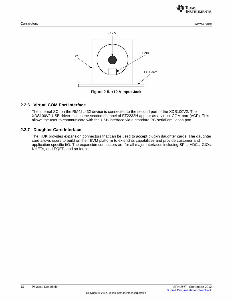
2.2.5 P1, +5 V to +12 V Input
Connector P1 is the input power connector. This connector brings +5V to +12 V to the HDK board. This isa 2.5 mm. jack. Figure 2-5 shows this connector as viewed from the card edge.
11SPNU567–September 2012 Physical DescriptionSubmit Documentation Feedback
Copyright © 2012, Texas Instruments Incorporated
texttext
P1
PC Board
GND
+12 V
Connectors www.ti.com
Figure 2-5. +12 V Input Jack
2.2.6 Virtual COM Port Interface
The internal SCI on the RM42L432 device is connected to the second port of the XDS100V2. TheXDS100V2 USB driver makes the second channel of FT2232H appear as a virtual COM port (VCP). Thisallows the user to communicate with the USB interface via a standard PC serial emulation port.
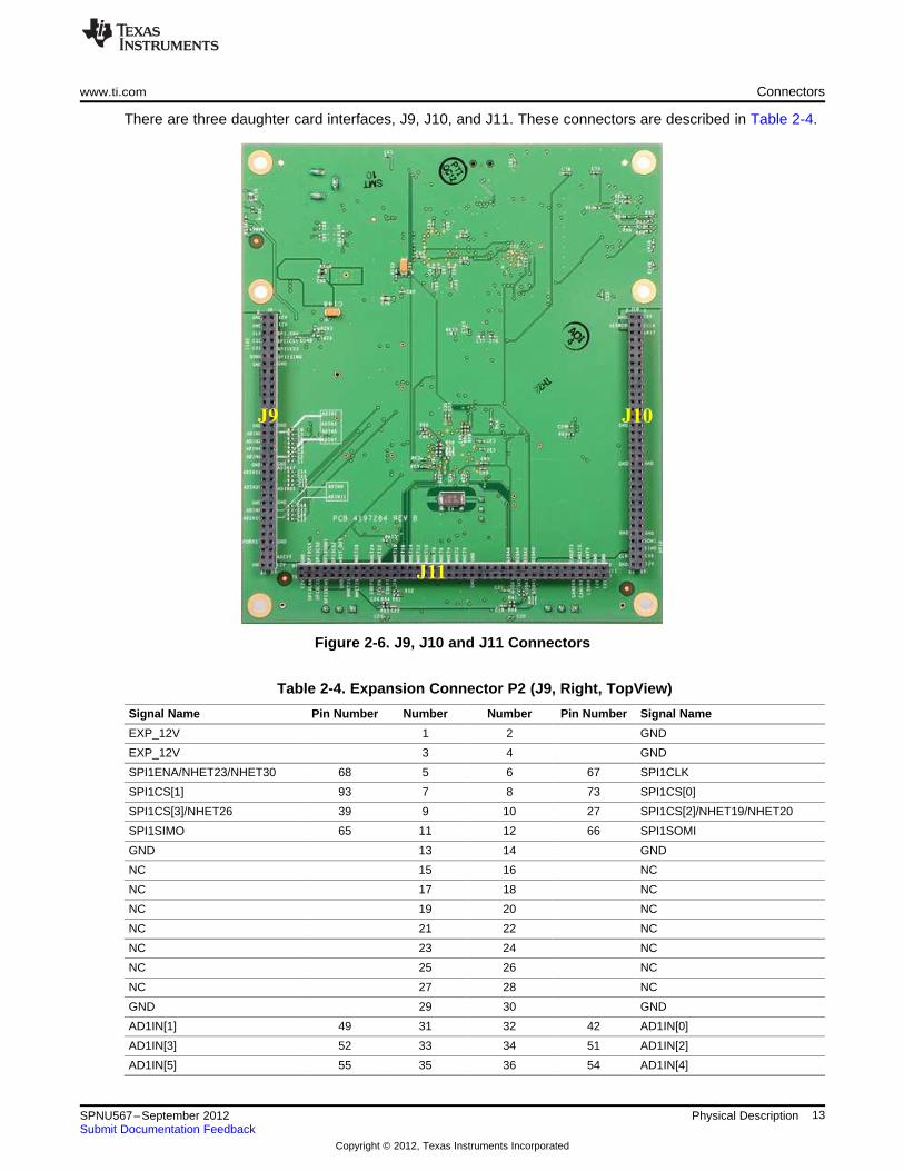
2.2.7 Daughter Card Interface
The HDK provides expansion connectors that can be used to accept plug-in daughter cards. The daughtercard allows users to build on their EVM platform to extend its capabilities and provide customer andapplication specific I/O. The expansion connectors are for all major interfaces including SPIs, ADCs, GIOs,NHETs, and EQEP, and so forth.
12 Physical Description SPNU567–September 2012Submit Documentation Feedback
Copyright © 2012, Texas Instruments Incorporated
J9 J10
J11
www.ti.com Connectors
There are three daughter card interfaces, J9, J10, and J11. These connectors are described in Table 2-4.
Figure 2-6. J9, J10 and J11 Connectors
Table 2-4. Expansion Connector P2 (J9, Right, TopView)
Signal Name Pin Number Number Number Pin Number Signal Name
EXP_12V 1 2 GND
EXP_12V 3 4 GND
SPI1ENA/NHET23/NHET30 68 5 6 67 SPI1CLK
SPI1CS[1] 93 7 8 73 SPI1CS[0]
SPI1CS[3]/NHET26 39 9 10 27 SPI1CS[2]/NHET19/NHET20
SPI1SIMO 65 11 12 66 SPI1SOMI
GND 13 14 GND
NC 15 16 NC
NC 17 18 NC
NC 19 20 NC
NC 21 22 NC
NC 23 24 NC
NC 25 26 NC
NC 27 28 NC
GND 29 30 GND
AD1IN[1] 49 31 32 42 AD1IN[0]
AD1IN[3] 52 33 34 51 AD1IN[2]
AD1IN[5] 55 35 36 54 AD1IN[4]
13SPNU567–September 2012 Physical DescriptionSubmit Documentation Feedback
Copyright © 2012, Texas Instruments Incorporated
Connectors www.ti.com
Table 2-4. Expansion Connector P2 (J9, Right, TopView) (continued)
Signal Name Pin Number Number Number Pin Number Signal Name
AD1IN[7] 43 37 38 56 AD1IN[6]
GND 39 40 GND
AD1IN[17] 41 41 42 40 AD1IN[16]
NC 43 44 NC
AD1IN[21] 45 45 46 44 AD1IN[20]
NC 47 48 NC
AGND 49 50 GND
AD1IN[9] 48 51 52 57 AD1IN[8]
AD1IN[11] 53 53 54 50 AD1IN[10]
NC 55 56 NC
NC 57 58 NC
GND 59 60 31 nPORRST
NC 61 62 NC
AD1EVT/NHET28 58 63 64 NC
EXP_12V 65 66 GND
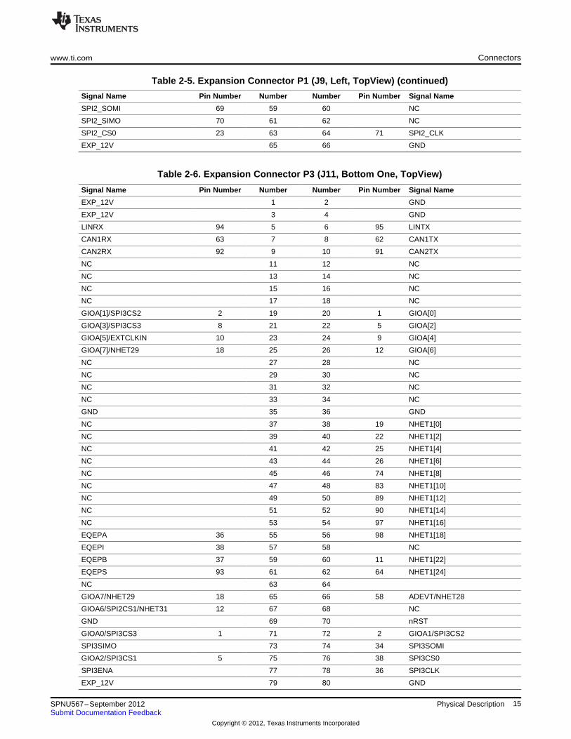
Table 2-5. Expansion Connector P1 (J9, Left, TopView)
Signal Name Pin Number Number Number Pin Number Signal Name
EXP_12V 1 2 GND
ECLK 84 3 4 82 nERROR
nRST 81 5 6 NC
NC 7 8 NC
NC 9 10 NC
NC 11 12 NC
NC 13 14 NC
NC 15 16 NC
NC 17 18 NC
NC 19 20 NC
NC 21 22 NC
NC 23 24 NC
NC 25 26 NC
NC 27 28 NC
GND 29 30 GND
NC 31 32 NC
NC 33 34 NC
NC 35 36 NC
NC 37 38 NC
GND 39 40 GND
NC 41 42 NC
NC 43 44 NC
NC 45 46 NC
NC 47 48 NC
NC 49 50 NC
NC 51 52 NC
NC 53 54 NC
NC 55 56 NC
GND 57 58 GND
14 Physical Description SPNU567–September 2012Submit Documentation Feedback
Copyright © 2012, Texas Instruments Incorporated
www.ti.com Connectors
Table 2-5. Expansion Connector P1 (J9, Left, TopView) (continued)
Signal Name Pin Number Number Number Pin Number Signal Name
SPI2_SOMI 69 59 60 NC
SPI2_SIMO 70 61 62 NC
SPI2_CS0 23 63 64 71 SPI2_CLK
EXP_12V 65 66 GND
Table 2-6. Expansion Connector P3 (J11, Bottom One, TopView)
Signal Name Pin Number Number Number Pin Number Signal Name
EXP_12V 1 2 GND
EXP_12V 3 4 GND
LINRX 94 5 6 95 LINTX
CAN1RX 63 7 8 62 CAN1TX
CAN2RX 92 9 10 91 CAN2TX
NC 11 12 NC
NC 13 14 NC
NC 15 16 NC
NC 17 18 NC
GIOA[1]/SPI3CS2 2 19 20 1 GIOA[0]
GIOA[3]/SPI3CS3 8 21 22 5 GIOA[2]
GIOA[5]/EXTCLKIN 10 23 24 9 GIOA[4]
GIOA[7]/NHET29 18 25 26 12 GIOA[6]
NC 27 28 NC
NC 29 30 NC
NC 31 32 NC
NC 33 34 NC
GND 35 36 GND
NC 37 38 19 NHET1[0]
NC 39 40 22 NHET1[2]
NC 41 42 25 NHET1[4]
NC 43 44 26 NHET1[6]
NC 45 46 74 NHET1[8]
NC 47 48 83 NHET1[10]
NC 49 50 89 NHET1[12]
NC 51 52 90 NHET1[14]
NC 53 54 97 NHET1[16]
EQEPA 36 55 56 98 NHET1[18]
EQEPI 38 57 58 NC
EQEPB 37 59 60 11 NHET1[22]
EQEPS 93 61 62 64 NHET1[24]
NC 63 64
GIOA7/NHET29 18 65 66 58 ADEVT/NHET28
GIOA6/SPI2CS1/NHET31 12 67 68 NC
GND 69 70 nRST
GIOA0/SPI3CS3 1 71 72 2 GIOA1/SPI3CS2
SPI3SIMO 73 74 34 SPI3SOMI
GIOA2/SPI3CS1 5 75 76 38 SPI3CS0
SPI3ENA 77 78 36 SPI3CLK
EXP_12V 79 80 GND
15SPNU567–September 2012 Physical DescriptionSubmit Documentation Feedback
Copyright © 2012, Texas Instruments Incorporated
1
2
12
12
LEDs www.ti.com
2.3 LEDs
The RM42 HDK board has fourteen (14) LEDs. Four of them are under user control. Those LEDs arecontrolled and programmed by GIO signals.
LED DS2, DS3, DS4, and DS5 indicate the presence of the power (+1.2 V, +5 V, 3.3 V, and 12 V) on theboard. The LED functions are summarized in Table 2-7 and Table 2-8.
Table 2-7. Demo LEDs
LED Number Location Signals Color
D2 Left Top GIOA6 White
D4 Left Bottom GIOA4 White
D5 Right Top GIOA3 White
D7 Right Bottom GIOA2 White
Table 2-8. Other LEDs as Indicator
Number LED Color
DS6 nERROR Red
D9 XDS100V2 SCI RX Blue
D8 XDS100V2 SCI TX Blue
D10 XDS100V2 PWRENn Blue
D1 JTAG TDI Blue
DS1 External JTAG Emulator Used Blue
DS5 VCC_1V2 Blue
DS3 VCC_5V Blue
DS2 VCC_3V3 Blue
DS4 VCC_12V Blue
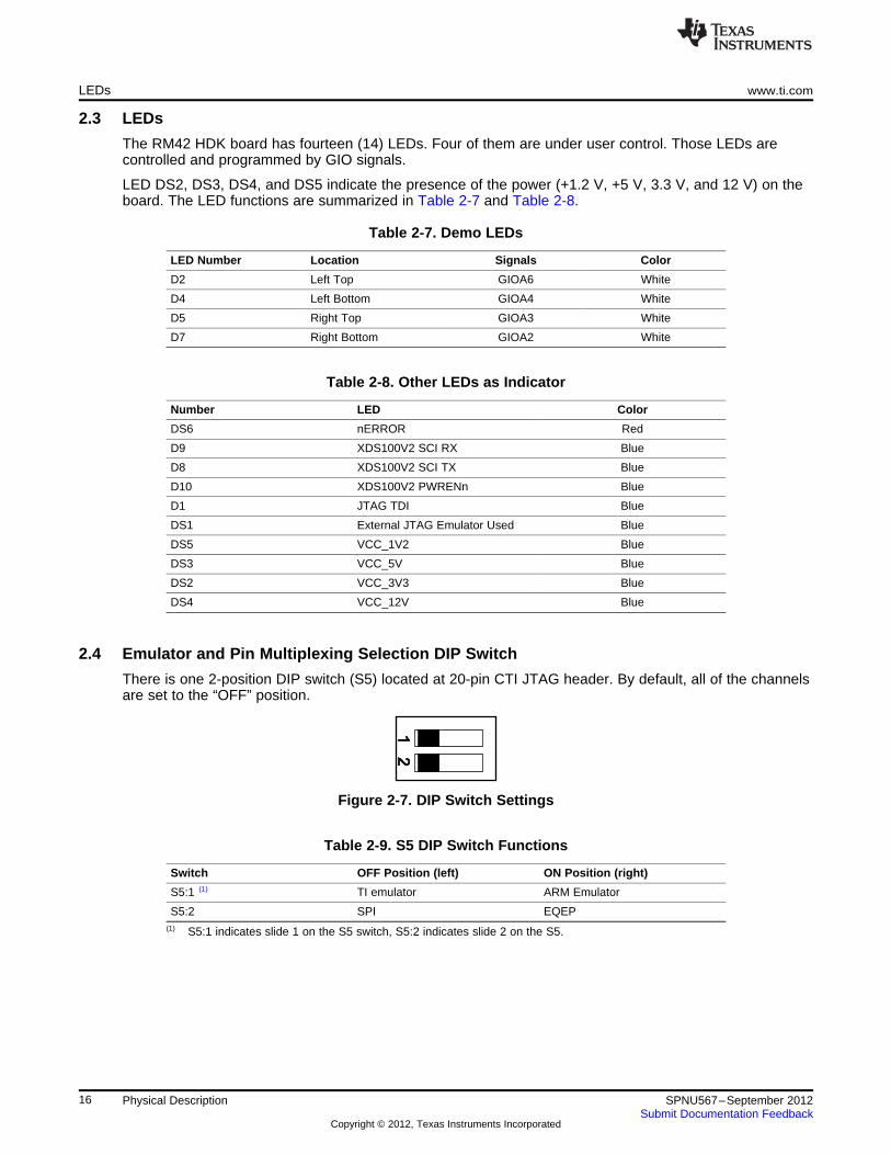
2.4 Emulator and Pin Multiplexing Selection DIP Switch
There is one 2-position DIP switch (S5) located at 20-pin CTI JTAG header. By default, all of the channelsare set to the “OFF” position.
Figure 2-7. DIP Switch Settings
Table 2-9. S5 DIP Switch Functions
Switch OFF Position (left) ON Position (right)
S5:1 (1) TI emulator ARM Emulator
S5:2 SPI EQEP(1) S5:1 indicates slide 1 on the S5 switch, S5:2 indicates slide 2 on the S5.
16 Physical Description SPNU567–September 2012Submit Documentation Feedback
Copyright © 2012, Texas Instruments Incorporated
www.ti.com Jumpers
2.5 Jumpers
HDK board has one jumper to select crystal or oscillator for MCU.
Table 2-10. Jumpers
Switch Position 1 - 2 Position 2 - 3
JP1 Oscillator Y3 Crystal Y2
2.6 S3, Power-On Reset Switch
RM42 MCU has two resets: Warm Reset (nRST) and Power-On Reset (nPORRST). Switch S3 is amomentary switch that asserts power on reset to the RM42L432 device. The nPORRST condition isintended to reset all logic on the device including the test and emulation circuitry.
2.7 S2, System Reset Switch
Switch S2 is used to assert a warm reset to reset the RM42L432 device. Warm reset does not reset anytest or emulation logic. The reset signal from window watchdog will also assert a warm reset to MCU. TheSystem Reset can be invoked by pushing nRST button, or by RESET signals from XDS100 CPLD, ARMJTAG SREST, and CTI JTAG SREST.
2.8 S4, Pushbutton for Clock Failure Test
Switch S4 is a momentary switch that will short the OSCIN pin of the crystal to ground through a currentlimiting resistor. Pushing this button simulates a crystal failure and causes a CLKDET hardware fault onMCU. By default this detection will trigger the Error Signaling Module (ESM) to drive the nERROR pin. OnRM42 HDK, the red LED will then light. The error can be cleared by the nPORRST (S3), cycling the powerto the MCU or via safety software executed on the MCU.
17SPNU567–September 2012 Physical DescriptionSubmit Documentation Feedback
Copyright © 2012, Texas Instruments Incorporated
Appendix ASPNU567–September 2012
Operation Notices
The user assumes all responsibility and liability for proper and safe handling of the boards. It is the user'sresponsibility to take any and all appropriate precautions with regard to electrostatic discharge.
A.1 Support Resources• If you have problems or need additional information regarding the embedded emulation please refer to
the XDS100 USB wiki on the TI web site. The URL for this site is:http://tiexpressdsp.com/index.php?title=XDS100
• Code Composer Studio support is available via a forum at: http://community.ti.com/forums/138.aspx
• Hercules MCU support is available via a forum at: http://www.ti.com/hercules-support
18 Operation Notices SPNU567–September 2012Submit Documentation Feedback
Copyright © 2012, Texas Instruments Incorporated
EVALUATION BOARD/KIT/MODULE (EVM) ADDITIONAL TERMS
Texas Instruments (TI) provides the enclosed Evaluation Board/Kit/Module (EVM) under the following conditions:
The user assumes all responsibility and liability for proper and safe handling of the goods. Further, the user indemnifies TI from all claimsarising from the handling or use of the goods.
Should this evaluation board/kit not meet the specifications indicated in the User’s Guide, the board/kit may be returned within 30 days fromthe date of delivery for a full refund. THE FOREGOING LIMITED WARRANTY IS THE EXCLUSIVE WARRANTY MADE BY SELLER TOBUYER AND IS IN LIEU OF ALL OTHER WARRANTIES, EXPRESSED, IMPLIED, OR STATUTORY, INCLUDING ANY WARRANTY OFMERCHANTABILITY OR FITNESS FOR ANY PARTICULAR PURPOSE. EXCEPT TO THE EXTENT OF THE INDEMNITY SET FORTHABOVE, NEITHER PARTY SHALL BE LIABLE TO THE OTHER FOR ANY INDIRECT, SPECIAL, INCIDENTAL, OR CONSEQUENTIALDAMAGES.
Please read the User's Guide and, specifically, the Warnings and Restrictions notice in the User's Guide prior to handling the product. Thisnotice contains important safety information about temperatures and voltages. For additional information on TI's environmental and/or safetyprograms, please visit www.ti.com/esh or contact TI.
No license is granted under any patent right or other intellectual property right of TI covering or relating to any machine, process, orcombination in which such TI products or services might be or are used. TI currently deals with a variety of customers for products, andtherefore our arrangement with the user is not exclusive. TI assumes no liability for applications assistance, customer product design,software performance, or infringement of patents or services described herein.
REGULATORY COMPLIANCE INFORMATION
As noted in the EVM User’s Guide and/or EVM itself, this EVM and/or accompanying hardware may or may not be subject to the FederalCommunications Commission (FCC) and Industry Canada (IC) rules.
For EVMs not subject to the above rules, this evaluation board/kit/module is intended for use for ENGINEERING DEVELOPMENT,DEMONSTRATION OR EVALUATION PURPOSES ONLY and is not considered by TI to be a finished end product fit for general consumeruse. It generates, uses, and can radiate radio frequency energy and has not been tested for compliance with the limits of computingdevices pursuant to part 15 of FCC or ICES-003 rules, which are designed to provide reasonable protection against radio frequencyinterference. Operation of the equipment may cause interference with radio communications, in which case the user at his own expense willbe required to take whatever measures may be required to correct this interference.
General Statement for EVMs including a radio
User Power/Frequency Use Obligations: This radio is intended for development/professional use only in legally allocated frequency andpower limits. Any use of radio frequencies and/or power availability of this EVM and its development application(s) must comply with locallaws governing radio spectrum allocation and power limits for this evaluation module. It is the user’s sole responsibility to only operate thisradio in legally acceptable frequency space and within legally mandated power limitations. Any exceptions to this are strictly prohibited andunauthorized by Texas Instruments unless user has obtained appropriate experimental/development licenses from local regulatoryauthorities, which is responsibility of user including its acceptable authorization.
For EVMs annotated as FCC – FEDERAL COMMUNICATIONS COMMISSION Part 15 Compliant
Caution
This device complies with part 15 of the FCC Rules. Operation is subject to the following two conditions: (1) This device may not causeharmful interference, and (2) this device must accept any interference received, including interference that may cause undesired operation.
Changes or modifications not expressly approved by the party responsible for compliance could void the user's authority to operate theequipment.
FCC Interference Statement for Class A EVM devices
This equipment has been tested and found to comply with the limits for a Class A digital device, pursuant to part 15 of the FCC Rules.These limits are designed to provide reasonable protection against harmful interference when the equipment is operated in a commercialenvironment. This equipment generates, uses, and can radiate radio frequency energy and, if not installed and used in accordance with theinstruction manual, may cause harmful interference to radio communications. Operation of this equipment in a residential area is likely tocause harmful interference in which case the user will be required to correct the interference at his own expense.
FCC Interference Statement for Class B EVM devices
This equipment has been tested and found to comply with the limits for a Class B digital device, pursuant to part 15 of the FCC Rules.These limits are designed to provide reasonable protection against harmful interference in a residential installation. This equipmentgenerates, uses and can radiate radio frequency energy and, if not installed and used in accordance with the instructions, may causeharmful interference to radio communications. However, there is no guarantee that interference will not occur in a particular installation. Ifthis equipment does cause harmful interference to radio or television reception, which can be determined by turning the equipment off andon, the user is encouraged to try to correct the interference by one or more of the following measures:
• Reorient or relocate the receiving antenna.• Increase the separation between the equipment and receiver.• Connect the equipment into an outlet on a circuit different from that to which the receiver is connected.• Consult the dealer or an experienced radio/TV technician for help.
For EVMs annotated as IC – INDUSTRY CANADA Compliant
This Class A or B digital apparatus complies with Canadian ICES-003.
Changes or modifications not expressly approved by the party responsible for compliance could void the user’s authority to operate theequipment.
Concerning EVMs including radio transmitters
This device complies with Industry Canada licence-exempt RSS standard(s). Operation is subject to the following two conditions: (1) thisdevice may not cause interference, and (2) this device must accept any interference, including interference that may cause undesiredoperation of the device.
Concerning EVMs including detachable antennas
Under Industry Canada regulations, this radio transmitter may only operate using an antenna of a type and maximum (or lesser) gainapproved for the transmitter by Industry Canada. To reduce potential radio interference to other users, the antenna type and its gain shouldbe so chosen that the equivalent isotropically radiated power (e.i.r.p.) is not more than that necessary for successful communication.
This radio transmitter has been approved by Industry Canada to operate with the antenna types listed in the user guide with the maximumpermissible gain and required antenna impedance for each antenna type indicated. Antenna types not included in this list, having a gaingreater than the maximum gain indicated for that type, are strictly prohibited for use with this device.
Cet appareil numérique de la classe A ou B est conforme à la norme NMB-003 du Canada.
Les changements ou les modifications pas expressément approuvés par la partie responsable de la conformité ont pu vider l’autorité del'utilisateur pour actionner l'équipement.
Concernant les EVMs avec appareils radio
Le présent appareil est conforme aux CNR d'Industrie Canada applicables aux appareils radio exempts de licence. L'exploitation estautorisée aux deux conditions suivantes : (1) l'appareil ne doit pas produire de brouillage, et (2) l'utilisateur de l'appareil doit accepter toutbrouillage radioélectrique subi, même si le brouillage est susceptible d'en compromettre le fonctionnement.
Concernant les EVMs avec antennes détachables
Conformément à la réglementation d'Industrie Canada, le présent émetteur radio peut fonctionner avec une antenne d'un type et d'un gainmaximal (ou inférieur) approuvé pour l'émetteur par Industrie Canada. Dans le but de réduire les risques de brouillage radioélectrique àl'intention des autres utilisateurs, il faut choisir le type d'antenne et son gain de sorte que la puissance isotrope rayonnée équivalente(p.i.r.e.) ne dépasse pas l'intensité nécessaire à l'établissement d'une communication satisfaisante.
Le présent émetteur radio a été approuvé par Industrie Canada pour fonctionner avec les types d'antenne énumérés dans le manueld’usage et ayant un gain admissible maximal et l'impédance requise pour chaque type d'antenne. Les types d'antenne non inclus danscette liste, ou dont le gain est supérieur au gain maximal indiqué, sont strictement interdits pour l'exploitation de l'émetteur.
SPACER
SPACER
SPACER
SPACER
SPACER
SPACER
SPACER
SPACER
【【Important Notice for Users of this Product in Japan】】This development kit is NOT certified as Confirming to Technical Regulations of Radio Law of Japan
If you use this product in Japan, you are required by Radio Law of Japan to follow the instructions below with respect to this product:
1. Use this product in a shielded room or any other test facility as defined in the notification #173 issued by Ministry of Internal Affairs andCommunications on March 28, 2006, based on Sub-section 1.1 of Article 6 of the Ministry’s Rule for Enforcement of Radio Law ofJapan,
2. Use this product only after you obtained the license of Test Radio Station as provided in Radio Law of Japan with respect to thisproduct, or
3. Use of this product only after you obtained the Technical Regulations Conformity Certification as provided in Radio Law of Japan withrespect to this product. Also, please do not transfer this product, unless you give the same notice above to the transferee. Please notethat if you could not follow the instructions above, you will be subject to penalties of Radio Law of Japan.
Texas Instruments Japan Limited(address) 24-1, Nishi-Shinjuku 6 chome, Shinjuku-ku, Tokyo, Japan
http://www.tij.co.jp
【ご使用にあたっての注】
本開発キットは技術基準適合証明を受けておりません。
本製品のご使用に際しては、電波法遵守のため、以下のいずれかの措置を取っていただく必要がありますのでご注意ください。1. 電波法施行規則第6条第1項第1号に基づく平成18年3月28日総務省告示第173号で定められた電波暗室等の試験設備でご使用いただく。2. 実験局の免許を取得後ご使用いただく。3. 技術基準適合証明を取得後ご使用いただく。
なお、本製品は、上記の「ご使用にあたっての注意」を譲渡先、移転先に通知しない限り、譲渡、移転できないものとします。
上記を遵守頂けない場合は、電波法の罰則が適用される可能性があることをご留意ください。
日本テキサス・インスツルメンツ株式会社東京都新宿区西新宿6丁目24番1号西新宿三井ビルhttp://www.tij.co.jp
SPACER
SPACER
SPACER
SPACER
SPACER
SPACER
SPACER
SPACER
SPACER
SPACER
SPACER
SPACER
SPACER
SPACER
SPACER
SPACER

EVALUATION BOARD/KIT/MODULE (EVM)WARNINGS, RESTRICTIONS AND DISCLAIMERS
For Feasibility Evaluation Only, in Laboratory/Development Environments. Unless otherwise indicated, this EVM is not a finishedelectrical equipment and not intended for consumer use. It is intended solely for use for preliminary feasibility evaluation inlaboratory/development environments by technically qualified electronics experts who are familiar with the dangers and application risksassociated with handling electrical mechanical components, systems and subsystems. It should not be used as all or part of a finished endproduct.
Your Sole Responsibility and Risk. You acknowledge, represent and agree that:
1. You have unique knowledge concerning Federal, State and local regulatory requirements (including but not limited to Food and DrugAdministration regulations, if applicable) which relate to your products and which relate to your use (and/or that of your employees,affiliates, contractors or designees) of the EVM for evaluation, testing and other purposes.
2. You have full and exclusive responsibility to assure the safety and compliance of your products with all such laws and other applicableregulatory requirements, and also to assure the safety of any activities to be conducted by you and/or your employees, affiliates,contractors or designees, using the EVM. Further, you are responsible to assure that any interfaces (electronic and/or mechanical)between the EVM and any human body are designed with suitable isolation and means to safely limit accessible leakage currents tominimize the risk of electrical shock hazard.
3. You will employ reasonable safeguards to ensure that your use of the EVM will not result in any property damage, injury or death, evenif the EVM should fail to perform as described or expected.
4. You will take care of proper disposal and recycling of the EVM’s electronic components and packing materials.
Certain Instructions. It is important to operate this EVM within TI’s recommended specifications and environmental considerations per theuser guidelines. Exceeding the specified EVM ratings (including but not limited to input and output voltage, current, power, andenvironmental ranges) may cause property damage, personal injury or death. If there are questions concerning these ratings please contacta TI field representative prior to connecting interface electronics including input power and intended loads. Any loads applied outside of thespecified output range may result in unintended and/or inaccurate operation and/or possible permanent damage to the EVM and/orinterface electronics. Please consult the EVM User's Guide prior to connecting any load to the EVM output. If there is uncertainty as to theload specification, please contact a TI field representative. During normal operation, some circuit components may have case temperaturesgreater than 60°C as long as the input and output are maintained at a normal ambient operating temperature. These components includebut are not limited to linear regulators, switching transistors, pass transistors, and current sense resistors which can be identified using theEVM schematic located in the EVM User's Guide. When placing measurement probes near these devices during normal operation, pleasebe aware that these devices may be very warm to the touch. As with all electronic evaluation tools, only qualified personnel knowledgeablein electronic measurement and diagnostics normally found in development environments should use these EVMs.
Agreement to Defend, Indemnify and Hold Harmless. You agree to defend, indemnify and hold TI, its licensors and their representativesharmless from and against any and all claims, damages, losses, expenses, costs and liabilities (collectively, "Claims") arising out of or inconnection with any use of the EVM that is not in accordance with the terms of the agreement. This obligation shall apply whether Claimsarise under law of tort or contract or any other legal theory, and even if the EVM fails to perform as described or expected.
Safety-Critical or Life-Critical Applications. If you intend to evaluate the components for possible use in safety critical applications (suchas life support) where a failure of the TI product would reasonably be expected to cause severe personal injury or death, such as deviceswhich are classified as FDA Class III or similar classification, then you must specifically notify TI of such intent and enter into a separateAssurance and Indemnity Agreement.
Mailing Address: Texas Instruments, Post Office Box 655303, Dallas, Texas 75265Copyright © 2012, Texas Instruments Incorporated

EVALUATION BOARD/KIT/MODULE (EVM) ADDITIONAL TERMSTexas Instruments (TI) provides the enclosed Evaluation Board/Kit/Module (EVM) under the following conditions:
The user assumes all responsibility and liability for proper and safe handling of the goods. Further, the user indemnifies TI from all claimsarising from the handling or use of the goods.
Should this evaluation board/kit not meet the specifications indicated in the User’s Guide, the board/kit may be returned within 30 days fromthe date of delivery for a full refund. THE FOREGOING LIMITED WARRANTY IS THE EXCLUSIVE WARRANTY MADE BY SELLER TOBUYER AND IS IN LIEU OF ALL OTHER WARRANTIES, EXPRESSED, IMPLIED, OR STATUTORY, INCLUDING ANY WARRANTY OFMERCHANTABILITY OR FITNESS FOR ANY PARTICULAR PURPOSE. EXCEPT TO THE EXTENT OF THE INDEMNITY SET FORTHABOVE, NEITHER PARTY SHALL BE LIABLE TO THE OTHER FOR ANY INDIRECT, SPECIAL, INCIDENTAL, OR CONSEQUENTIALDAMAGES.
Please read the User's Guide and, specifically, the Warnings and Restrictions notice in the User's Guide prior to handling the product. Thisnotice contains important safety information about temperatures and voltages. For additional information on TI's environmental and/or safetyprograms, please visit www.ti.com/esh or contact TI.
No license is granted under any patent right or other intellectual property right of TI covering or relating to any machine, process, orcombination in which such TI products or services might be or are used. TI currently deals with a variety of customers for products, andtherefore our arrangement with the user is not exclusive. TI assumes no liability for applications assistance, customer product design,software performance, or infringement of patents or services described herein.
REGULATORY COMPLIANCE INFORMATIONAs noted in the EVM User’s Guide and/or EVM itself, this EVM and/or accompanying hardware may or may not be subject to the FederalCommunications Commission (FCC) and Industry Canada (IC) rules.
For EVMs not subject to the above rules, this evaluation board/kit/module is intended for use for ENGINEERING DEVELOPMENT,DEMONSTRATION OR EVALUATION PURPOSES ONLY and is not considered by TI to be a finished end product fit for general consumeruse. It generates, uses, and can radiate radio frequency energy and has not been tested for compliance with the limits of computingdevices pursuant to part 15 of FCC or ICES-003 rules, which are designed to provide reasonable protection against radio frequencyinterference. Operation of the equipment may cause interference with radio communications, in which case the user at his own expense willbe required to take whatever measures may be required to correct this interference.
General Statement for EVMs including a radioUser Power/Frequency Use Obligations: This radio is intended for development/professional use only in legally allocated frequency andpower limits. Any use of radio frequencies and/or power availability of this EVM and its development application(s) must comply with locallaws governing radio spectrum allocation and power limits for this evaluation module. It is the user’s sole responsibility to only operate thisradio in legally acceptable frequency space and within legally mandated power limitations. Any exceptions to this are strictly prohibited andunauthorized by Texas Instruments unless user has obtained appropriate experimental/development licenses from local regulatoryauthorities, which is responsibility of user including its acceptable authorization.
For EVMs annotated as FCC – FEDERAL COMMUNICATIONS COMMISSION Part 15 Compliant
CautionThis device complies with part 15 of the FCC Rules. Operation is subject to the following two conditions: (1) This device may not causeharmful interference, and (2) this device must accept any interference received, including interference that may cause undesired operation.
Changes or modifications not expressly approved by the party responsible for compliance could void the user's authority to operate theequipment.
FCC Interference Statement for Class A EVM devicesThis equipment has been tested and found to comply with the limits for a Class A digital device, pursuant to part 15 of the FCC Rules.These limits are designed to provide reasonable protection against harmful interference when the equipment is operated in a commercialenvironment. This equipment generates, uses, and can radiate radio frequency energy and, if not installed and used in accordance with theinstruction manual, may cause harmful interference to radio communications. Operation of this equipment in a residential area is likely tocause harmful interference in which case the user will be required to correct the interference at his own expense.
FCC Interference Statement for Class B EVM devicesThis equipment has been tested and found to comply with the limits for a Class B digital device, pursuant to part 15 of the FCC Rules.These limits are designed to provide reasonable protection against harmful interference in a residential installation. This equipmentgenerates, uses and can radiate radio frequency energy and, if not installed and used in accordance with the instructions, may causeharmful interference to radio communications. However, there is no guarantee that interference will not occur in a particular installation. Ifthis equipment does cause harmful interference to radio or television reception, which can be determined by turning the equipment off andon, the user is encouraged to try to correct the interference by one or more of the following measures:
• Reorient or relocate the receiving antenna.• Increase the separation between the equipment and receiver.• Connect the equipment into an outlet on a circuit different from that to which the receiver is connected.• Consult the dealer or an experienced radio/TV technician for help.
For EVMs annotated as IC – INDUSTRY CANADA Compliant
This Class A or B digital apparatus complies with Canadian ICES-003.
Changes or modifications not expressly approved by the party responsible for compliance could void the user’s authority to operate theequipment.
Concerning EVMs including radio transmitters
This device complies with Industry Canada licence-exempt RSS standard(s). Operation is subject to the following two conditions: (1) thisdevice may not cause interference, and (2) this device must accept any interference, including interference that may cause undesiredoperation of the device.
Concerning EVMs including detachable antennasUnder Industry Canada regulations, this radio transmitter may only operate using an antenna of a type and maximum (or lesser) gainapproved for the transmitter by Industry Canada. To reduce potential radio interference to other users, the antenna type and its gain shouldbe so chosen that the equivalent isotropically radiated power (e.i.r.p.) is not more than that necessary for successful communication.
This radio transmitter has been approved by Industry Canada to operate with the antenna types listed in the user guide with the maximumpermissible gain and required antenna impedance for each antenna type indicated. Antenna types not included in this list, having a gaingreater than the maximum gain indicated for that type, are strictly prohibited for use with this device.
Cet appareil numérique de la classe A ou B est conforme à la norme NMB-003 du Canada.
Les changements ou les modifications pas expressément approuvés par la partie responsable de la conformité ont pu vider l’autorité del'utilisateur pour actionner l'équipement.
Concernant les EVMs avec appareils radio
Le présent appareil est conforme aux CNR d'Industrie Canada applicables aux appareils radio exempts de licence. L'exploitation estautorisée aux deux conditions suivantes : (1) l'appareil ne doit pas produire de brouillage, et (2) l'utilisateur de l'appareil doit accepter toutbrouillage radioélectrique subi, même si le brouillage est susceptible d'en compromettre le fonctionnement.
Concernant les EVMs avec antennes détachables
Conformément à la réglementation d'Industrie Canada, le présent émetteur radio peut fonctionner avec une antenne d'un type et d'un gainmaximal (ou inférieur) approuvé pour l'émetteur par Industrie Canada. Dans le but de réduire les risques de brouillage radioélectrique àl'intention des autres utilisateurs, il faut choisir le type d'antenne et son gain de sorte que la puissance isotrope rayonnée équivalente(p.i.r.e.) ne dépasse pas l'intensité nécessaire à l'établissement d'une communication satisfaisante.
Le présent émetteur radio a été approuvé par Industrie Canada pour fonctionner avec les types d'antenne énumérés dans le manueld’usage et ayant un gain admissible maximal et l'impédance requise pour chaque type d'antenne. Les types d'antenne non inclus danscette liste, ou dont le gain est supérieur au gain maximal indiqué, sont strictement interdits pour l'exploitation de l'émetteur.
SPACER
SPACER
SPACER
SPACER
SPACER
SPACER
SPACER
SPACER

【【Important Notice for Users of this Product in Japan】】This development kit is NOT certified as Confirming to Technical Regulations of Radio Law of Japan
If you use this product in Japan, you are required by Radio Law of Japan to follow the instructions below with respect to this product:
1. Use this product in a shielded room or any other test facility as defined in the notification #173 issued by Ministry of Internal Affairs andCommunications on March 28, 2006, based on Sub-section 1.1 of Article 6 of the Ministry’s Rule for Enforcement of Radio Law ofJapan,
2. Use this product only after you obtained the license of Test Radio Station as provided in Radio Law of Japan with respect to thisproduct, or
3. Use of this product only after you obtained the Technical Regulations Conformity Certification as provided in Radio Law of Japan withrespect to this product. Also, please do not transfer this product, unless you give the same notice above to the transferee. Please notethat if you could not follow the instructions above, you will be subject to penalties of Radio Law of Japan.
Texas Instruments Japan Limited(address) 24-1, Nishi-Shinjuku 6 chome, Shinjuku-ku, Tokyo, Japan
http://www.tij.co.jp
【ご使用にあたっての注】
本開発キットは技術基準適合証明を受けておりません。
本製品のご使用に際しては、電波法遵守のため、以下のいずれかの措置を取っていただく必要がありますのでご注意ください。1. 電波法施行規則第6条第1項第1号に基づく平成18年3月28日総務省告示第173号で定められた電波暗室等の試験設備でご使用いただく。2. 実験局の免許を取得後ご使用いただく。3. 技術基準適合証明を取得後ご使用いただく。
なお、本製品は、上記の「ご使用にあたっての注意」を譲渡先、移転先に通知しない限り、譲渡、移転できないものとします。
上記を遵守頂けない場合は、電波法の罰則が適用される可能性があることをご留意ください。
日本テキサス・インスツルメンツ株式会社東京都新宿区西新宿6丁目24番1号西新宿三井ビルhttp://www.tij.co.jp
SPACER
SPACER
SPACER
SPACER
SPACER
SPACER
SPACER
SPACER
SPACER
SPACER
SPACER
SPACER
SPACER
SPACER
SPACER
SPACER
EVALUATION BOARD/KIT/MODULE (EVM)WARNINGS, RESTRICTIONS AND DISCLAIMERS
For Feasibility Evaluation Only, in Laboratory/Development Environments. Unless otherwise indicated, this EVM is not a finishedelectrical equipment and not intended for consumer use. It is intended solely for use for preliminary feasibility evaluation inlaboratory/development environments by technically qualified electronics experts who are familiar with the dangers and application risksassociated with handling electrical mechanical components, systems and subsystems. It should not be used as all or part of a finished endproduct.
Your Sole Responsibility and Risk. You acknowledge, represent and agree that:
1. You have unique knowledge concerning Federal, State and local regulatory requirements (including but not limited to Food and DrugAdministration regulations, if applicable) which relate to your products and which relate to your use (and/or that of your employees,affiliates, contractors or designees) of the EVM for evaluation, testing and other purposes.
2. You have full and exclusive responsibility to assure the safety and compliance of your products with all such laws and other applicableregulatory requirements, and also to assure the safety of any activities to be conducted by you and/or your employees, affiliates,contractors or designees, using the EVM. Further, you are responsible to assure that any interfaces (electronic and/or mechanical)between the EVM and any human body are designed with suitable isolation and means to safely limit accessible leakage currents tominimize the risk of electrical shock hazard.
3. You will employ reasonable safeguards to ensure that your use of the EVM will not result in any property damage, injury or death, evenif the EVM should fail to perform as described or expected.
4. You will take care of proper disposal and recycling of the EVM’s electronic components and packing materials.
Certain Instructions. It is important to operate this EVM within TI’s recommended specifications and environmental considerations per theuser guidelines. Exceeding the specified EVM ratings (including but not limited to input and output voltage, current, power, andenvironmental ranges) may cause property damage, personal injury or death. If there are questions concerning these ratings please contacta TI field representative prior to connecting interface electronics including input power and intended loads. Any loads applied outside of thespecified output range may result in unintended and/or inaccurate operation and/or possible permanent damage to the EVM and/orinterface electronics. Please consult the EVM User's Guide prior to connecting any load to the EVM output. If there is uncertainty as to theload specification, please contact a TI field representative. During normal operation, some circuit components may have case temperaturesgreater than 60°C as long as the input and output are maintained at a normal ambient operating temperature. These components includebut are not limited to linear regulators, switching transistors, pass transistors, and current sense resistors which can be identified using theEVM schematic located in the EVM User's Guide. When placing measurement probes near these devices during normal operation, pleasebe aware that these devices may be very warm to the touch. As with all electronic evaluation tools, only qualified personnel knowledgeablein electronic measurement and diagnostics normally found in development environments should use these EVMs.
Agreement to Defend, Indemnify and Hold Harmless. You agree to defend, indemnify and hold TI, its licensors and their representativesharmless from and against any and all claims, damages, losses, expenses, costs and liabilities (collectively, "Claims") arising out of or inconnection with any use of the EVM that is not in accordance with the terms of the agreement. This obligation shall apply whether Claimsarise under law of tort or contract or any other legal theory, and even if the EVM fails to perform as described or expected.
Safety-Critical or Life-Critical Applications. If you intend to evaluate the components for possible use in safety critical applications (suchas life support) where a failure of the TI product would reasonably be expected to cause severe personal injury or death, such as deviceswhich are classified as FDA Class III or similar classification, then you must specifically notify TI of such intent and enter into a separateAssurance and Indemnity Agreement.
Mailing Address: Texas Instruments, Post Office Box 655303, Dallas, Texas 75265Copyright © 2012, Texas Instruments Incorporated
IMPORTANT NOTICE
Texas Instruments Incorporated and its subsidiaries (TI) reserve the right to make corrections, enhancements, improvements and otherchanges to its semiconductor products and services per JESD46, latest issue, and to discontinue any product or service per JESD48, latestissue. Buyers should obtain the latest relevant information before placing orders and should verify that such information is current andcomplete. All semiconductor products (also referred to herein as “components”) are sold subject to TI’s terms and conditions of salesupplied at the time of order acknowledgment.
TI warrants performance of its components to the specifications applicable at the time of sale, in accordance with the warranty in TI’s termsand conditions of sale of semiconductor products. Testing and other quality control techniques are used to the extent TI deems necessaryto support this warranty. Except where mandated by applicable law, testing of all parameters of each component is not necessarilyperformed.
TI assumes no liability for applications assistance or the design of Buyers’ products. Buyers are responsible for their products andapplications using TI components. To minimize the risks associated with Buyers’ products and applications, Buyers should provideadequate design and operating safeguards.
TI does not warrant or represent that any license, either express or implied, is granted under any patent right, copyright, mask work right, orother intellectual property right relating to any combination, machine, or process in which TI components or services are used. Informationpublished by TI regarding third-party products or services does not constitute a license to use such products or services or a warranty orendorsement thereof. Use of such information may require a license from a third party under the patents or other intellectual property of thethird party, or a license from TI under the patents or other intellectual property of TI.
Reproduction of significant portions of TI information in TI data books or data sheets is permissible only if reproduction is without alterationand is accompanied by all associated warranties, conditions, limitations, and notices. TI is not responsible or liable for such altereddocumentation. Information of third parties may be subject to additional restrictions.
Resale of TI components or services with statements different from or beyond the parameters stated by TI for that component or servicevoids all express and any implied warranties for the associated TI component or service and is an unfair and deceptive business practice.TI is not responsible or liable for any such statements.
Buyer acknowledges and agrees that it is solely responsible for compliance with all legal, regulatory and safety-related requirementsconcerning its products, and any use of TI components in its applications, notwithstanding any applications-related information or supportthat may be provided by TI. Buyer represents and agrees that it has all the necessary expertise to create and implement safeguards whichanticipate dangerous consequences of failures, monitor failures and their consequences, lessen the likelihood of failures that might causeharm and take appropriate remedial actions. Buyer will fully indemnify TI and its representatives against any damages arising out of the useof any TI components in safety-critical applications.
In some cases, TI components may be promoted specifically to facilitate safety-related applications. With such components, TI’s goal is tohelp enable customers to design and create their own end-product solutions that meet applicable functional safety standards andrequirements. Nonetheless, such components are subject to these terms.
No TI components are authorized for use in FDA Class III (or similar life-critical medical equipment) unless authorized officers of the partieshave executed a special agreement specifically governing such use.
Only those TI components which TI has specifically designated as military grade or “enhanced plastic” are designed and intended for use inmilitary/aerospace applications or environments. Buyer acknowledges and agrees that any military or aerospace use of TI componentswhich have not been so designated is solely at the Buyer's risk, and that Buyer is solely responsible for compliance with all legal andregulatory requirements in connection with such use.
TI has specifically designated certain components which meet ISO/TS16949 requirements, mainly for automotive use. Components whichhave not been so designated are neither designed nor intended for automotive use; and TI will not be responsible for any failure of suchcomponents to meet such requirements.
Products Applications
Audio www.ti.com/audio Automotive and Transportation www.ti.com/automotive
Amplifiers amplifier.ti.com Communications and Telecom www.ti.com/communications
Data Converters dataconverter.ti.com Computers and Peripherals www.ti.com/computers
DLP® Products www.dlp.com Consumer Electronics www.ti.com/consumer-apps
DSP dsp.ti.com Energy and Lighting www.ti.com/energy
Clocks and Timers www.ti.com/clocks Industrial www.ti.com/industrial
Interface interface.ti.com Medical www.ti.com/medical
Logic logic.ti.com Security www.ti.com/security
Power Mgmt power.ti.com Space, Avionics and Defense www.ti.com/space-avionics-defense
Microcontrollers microcontroller.ti.com Video and Imaging www.ti.com/video
RFID www.ti-rfid.com
OMAP Applications Processors www.ti.com/omap TI E2E Community e2e.ti.com
Wireless Connectivity www.ti.com/wirelessconnectivity
Mailing Address: Texas Instruments, Post Office Box 655303, Dallas, Texas 75265Copyright © 2012, Texas Instruments Incorporated
Related Documents