Introduction to RF Power Amplifier Design and Simulation

Welcome message from author
This document is posted to help you gain knowledge. Please leave a comment to let me know what you think about it! Share it to your friends and learn new things together.
Transcript

I n t r o d u c t i o n t oRF Power AmplifierDesign and Simulation

CRC Press is an imprint of theTaylor & Francis Group, an informa business
Boca Raton London New York
I n t r o d u c t i o n t oRF Power AmplifierDesign and Simulation
A b d u l l a h E r o g l uI N D I A N A U N I V E R S I T Y – P U R D U E U N I V E R S I T Y
F O R T W A Y N E , I N , U S A

MATLAB® and Simulink® are trademarks of The MathWorks, Inc. and are used with permission. The MathWorks does not warrant the accuracy of the text or exercises in this book. This book’s use or discussion of MATLAB® and Simulink® software or related products does not constitute endorsement or sponsorship by The MathWorks of a particular pedagogical approach or particular use of the MAT-LAB® and Simulink® software.
CRC PressTaylor & Francis Group6000 Broken Sound Parkway NW, Suite 300Boca Raton, FL 33487-2742
© 2016 by Taylor & Francis Group, LLCCRC Press is an imprint of Taylor & Francis Group, an Informa business
No claim to original U.S. Government worksVersion Date: 20150312
International Standard Book Number-13: 978-1-4822-3165-6 (eBook - PDF)
This book contains information obtained from authentic and highly regarded sources. Reasonable efforts have been made to publish reliable data and information, but the author and publisher cannot assume responsibility for the validity of all materials or the consequences of their use. The authors and publishers have attempted to trace the copyright holders of all material reproduced in this publication and apologize to copyright holders if permission to publish in this form has not been obtained. If any copyright material has not been acknowledged please write and let us know so we may rectify in any future reprint.
Except as permitted under U.S. Copyright Law, no part of this book may be reprinted, reproduced, transmitted, or utilized in any form by any electronic, mechanical, or other means, now known or hereafter invented, including photocopying, microfilming, and recording, or in any information stor-age or retrieval system, without written permission from the publishers.
For permission to photocopy or use material electronically from this work, please access www.copy-right.com (http://www.copyright.com/) or contact the Copyright Clearance Center, Inc. (CCC), 222 Rosewood Drive, Danvers, MA 01923, 978-750-8400. CCC is a not-for-profit organization that pro-vides licenses and registration for a variety of users. For organizations that have been granted a photo-copy license by the CCC, a separate system of payment has been arranged.
Trademark Notice: Product or corporate names may be trademarks or registered trademarks, and are used only for identification and explanation without intent to infringe.
Visit the Taylor & Francis Web site athttp://www.taylorandfrancis.com
and the CRC Press Web site athttp://www.crcpress.com

Dedicated to my sons, Duhan and Enes, and daughter Dilem

vii
ContentsPreface.................................................................................................................... xiiiAcknowledgments ....................................................................................................xvAuthor ....................................................................................................................xvii
Chapter 1 Radio Frequency Amplifier Basics.......................................................1
1.1 Introduction ...............................................................................11.2 RF Amplifier Terminology ........................................................5
1.2.1 Gain ..............................................................................51.2.2 Efficiency ......................................................................81.2.3 Power Output Capability ..............................................91.2.4 Linearity .......................................................................91.2.5 1-dB Compression Point ............................................. 10
1.3 Small-Signal vs. Large-Signal Characteristics ........................ 111.3.1 Harmonic Distortion .................................................. 121.3.2 Intermodulation .......................................................... 15
1.4 RF Amplifier Classifications ...................................................251.4.1 Conventional Amplifiers—Classes A, B, and C ........29
1.4.1.1 Class A ........................................................ 331.4.1.2 Class B ........................................................341.4.1.3 Class AB .....................................................361.4.1.4 Class C ........................................................36
1.4.2 Switch-Mode Amplifiers—Classes D, E, and F ........ 371.4.2.1 Class D ........................................................ 381.4.2.2 Class E ........................................................401.4.2.3 Class DE ..................................................... 411.4.2.4 Class F ........................................................ 421.4.2.5 Class S ........................................................ 45
1.5 High-Power RF Amplifier Design Techniques ........................ 451.5.1 Push–Pull Amplifier Configuration ........................... 471.5.2 Parallel Transistor Configuration ............................... 471.5.3 PA Module Combiners ............................................... 49
1.6 RF Power Transistors ..............................................................501.7 CAD Tools in RF Amplifier Design ........................................ 51References .......................................................................................... 59
Chapter 2 Radio Frequency Power Transistors ................................................... 61
2.1 Introduction ............................................................................. 612.2 High-Frequency Model for MOSFETs .................................... 61
viii Contents
2.3 Use of Simulation to Obtain Internal Capacitances of MOSFETs ............................................................................ 712.3.1 Finding Ciss with PSpice ............................................. 712.3.2 Finding Coss and Crss with PSpice ............................... 72
2.4 Transient Characteristics of MOSFET .................................... 752.4.1 During Turn-On ......................................................... 752.4.2 During Turn-Off ......................................................... 79
2.5 Losses for MOSFET ................................................................ 832.6 Thermal Characteristics of MOSFETs ....................................842.7 Safe Operating Area for MOSFETs ........................................872.8 MOSFET Gate Threshold and Plateau Voltage .......................88References .......................................................................................... 91
Chapter 3 Transistor Modeling and Simulation ..................................................93
3.1 Introduction .............................................................................933.2 Network Parameters ................................................................93
3.2.1 Z-Impedance Parameters ...........................................933.2.2 Y-Admittance Parameters ...........................................943.2.3 ABCD-Parameters ......................................................953.2.4 h-Hybrid Parameters ..................................................96
3.3 Network Connections ............................................................ 1033.3.1 MATLAB® Implementation of Network Parameters ...111
3.4 S-Scattering Parameters ........................................................ 1233.4.1 One-Port Network .................................................... 1233.4.2 N-Port Network ........................................................ 1253.4.3 Normalized Scattering Parameters .......................... 130
3.5 Measurement of S Parameters ............................................... 1433.5.1 Measurement of S Parameters for a Two-Port
Network .................................................................... 1433.5.2 Measurement of S Parameters for a Three-Port
Network .................................................................... 1453.5.3 Design and Calibration Methods for
Measurement of Transistor Scattering Parameters ... 1483.5.3.1 Design of SOLT Test Fixtures Using
Grounded Coplanar Waveguide Structure ... 1513.6 Chain Scattering Parameters ................................................. 1653.7 Systematizing RF Amplifier Design by Network Analysis ... 1693.8 Extraction of Parasitics for MOSFET Devices ...................... 174
3.8.1 De-Embedding Techniques ...................................... 1833.8.2 De-Embedding Technique with Static Approach ..... 1863.8.3 De-Embedding Technique with Real-Time
Approach .................................................................. 187References ........................................................................................ 194
ixContents
Chapter 4 Resonator Networks for Amplifiers.................................................. 197
4.1 Introduction ........................................................................... 1974.2 Parallel and Series Resonant Networks ................................. 197
4.2.1 Parallel Resonance ................................................... 1974.2.2 Series Resonance ......................................................205
4.3 Practical Resonances with Loss, Loading, and Coupling Effects ....................................................................................2094.3.1 Component Resonances ...........................................2094.3.2 Parallel LC Networks ............................................... 216
4.3.2.1 Parallel LC Networks with Ideal Components .............................................. 216
4.3.2.2 Parallel LC Networks with Non-Ideal Components .............................................. 219
4.3.2.3 Loading Effects on Parallel LC Networks ...2204.3.2.4 LC Network Transformations ................... 2234.3.2.5 LC Network with Series Loss ...................228
4.4 Coupling of Resonators ......................................................... 2294.5 LC Resonators as Impedance Transformers..........................234
4.5.1 Inductive Load ..........................................................2344.5.2 Capacitive Load ........................................................ 235
4.6 Tapped Resonators as Impedance Transformers ................... 2394.6.1 Tapped-C Impedance Transformer .......................... 2394.6.2 Tapped-L Impedance Transformer ...........................244
Reference ..........................................................................................260
Chapter 5 Impedance Matching Networks ....................................................... 261
5.1 Introduction ........................................................................... 2615.2 Transmission Lines ................................................................ 261
5.2.1 Limiting Cases for Transmission Lines ...................2665.2.2 Terminated Lossless Transmission Lines.................2685.2.3 Special Cases of Terminated Transmission Lines ... 274
5.3 Smith Chart ........................................................................... 2765.3.1 Input Impedance Determination with Smith Chart ...2825.3.2 Smith Chart as an Admittance Chart .......................2855.3.3 ZY Smith Chart and Its Application .........................287
5.4 Impedance Matching between Transmission Lines and Load Impedances .................................................................. 289
5.5 Single-Stub Tuning ................................................................2925.5.1 Shunt Single-Stub Tuning ........................................2925.5.2 Series Single-Stub Tuning ........................................294
5.6 Impedance Transformation and Matching between Source and Load Impedances ...............................................296
5.7 Signal Flow Graphs ...............................................................299Reference ..........................................................................................305
x Contents
Chapter 6 Couplers, Multistate Reflectometers, and RF Power Sensors for Amplifiers ...................................................................................307
6.1 Introduction ...........................................................................3076.2 Directional Couplers ..............................................................307
6.2.1 Microstrip Directional Couplers .............................. 3106.2.1.1 Two-Line Microstrip Directional
Couplers .................................................... 3106.2.1.2 Three-Line Microstrip Directional
Couplers .................................................... 3166.2.2 Multilayer Planar Directional Couplers ................... 3206.2.3 Transformer-Coupled Directional Couplers ............. 323
6.2.3.1 Four-Port Directional Coupler Design and Implementation .................................. 325
6.2.3.2 Six-Port Directional Coupler Design and Implementation .................................. 327
6.3 Multistate Reflectometers ...................................................... 3426.3.1 Multistate Reflectometer Based on Four-Port
Network and Variable Attenuator............................. 3436.4 RF Power Sensors .................................................................. 347References ........................................................................................ 352
Chapter 7 Filter Design for RF Power Amplifiers ............................................ 355
7.1 Introduction ........................................................................... 3557.2 Filter Design by Insertion Loss Method ................................ 357
7.2.1 Low Pass Filters ....................................................... 3577.2.1.1 Binomial Filter Response ......................... 3587.2.1.2 Chebyshev Filter Response ....................... 361
7.2.2 High-Pass Filters ...................................................... 3687.2.3 Bandpass Filters ....................................................... 3687.2.4 Bandstop Filters ........................................................ 369
7.3 Stepped-Impedance LPFs ...................................................... 3707.4 Stepped-Impedance Resonator BPFs .................................... 3747.5 Edge/Parallel-Coupled, Half-Wavelength Resonator BPFs ... 3777.6 End-Coupled, Capacitive Gap, Half-Wavelength
Resonator BPFs...................................................................... 387References ........................................................................................ 398
Chapter 8 Computer Aided Design Tools for Amplifier Design and Implementation .......................................................................... 399
8.1 Introduction ........................................................................... 3998.2 Passive Component Design and Modeling with CAD—
Combiners .............................................................................. 4018.2.1 Analysis Phase for Combiners ................................. 401

xiContents
8.2.2 Simulation Phase for Combiners ..............................4088.2.3 Experimental Phase for Combiners .......................... 411
8.3 Active Component Design and Modeling with CAD ............ 4138.3.1 Analysis Phase for Hybrid Package.......................... 4148.3.2 Simulation Phase for Hybrid Package ...................... 4168.3.3 Experimental Phase for Hybrid Package .................. 420
References ........................................................................................ 420
Index ...................................................................................................................... 423


xiii
PrefaceRadio frequency (RF) power amplifiers are used in everyday life for many applica-tions including cellular phones, magnetic resonance imaging, semiconductor wafer processing for chip manufacturing, etc. Therefore, the design and performance of RF amplifiers carry great importance for the proper functionality of these devices. Furthermore, several industrial and military applications require low-profile yet high-powered and efficient power amplifiers. This is a challenging task when several components are needed to be considered in the design of RF power amplifiers to meet the required criteria. As a result, designers are in need of a resource to provide all the essential design components for better-performing, low-profile, high-power, and efficient RF power amplifiers. This book is intended to be the main resource for engineers and students and fill the existing gap in the area of RF power ampli-fier design by giving a complete guidance with demonstration of the details for the design stages including analytical formulation and simulation. Therefore, in addition to the fact that it can be used as a unique resource for engineers and researchers, this book can also be used as a textbook for RF/microwave engineering students in their senior year at college. Chapter end problems are given to make this option feasible for instructors and students.
Successful realization of RF power amplifiers depends on the transition between each design stage. This book provides practical hints to accomplish the transition between the design stages with illustrations and examples. An analytical formulation to design the amplifier and computer-aided design (CAD) tools to verify the design, have been detailed with a step-by-step design process that makes this book easy to follow. The extensive coverage of the book includes not only an introduction to the design of several amplifier topologies; it also includes the design and simulation of amplifier’s surrounding sections and assemblies. This book also focuses on the higher-level design sections and assemblies for RF amplifiers, which make the book unique and essential for the designer to accomplish the amplifier design as per the given specifications.
The scope of each chapter in this book can be summarized as follows. Chapter 1 provides an introduction to RF power amplifier basics and topologies. It also gives a brief overview of intermodulation and elaborates discussion on the difference between linear and nonlinear amplifiers. Chapter 2 gives details on the high-frequency model and transient characteristics of metal–oxide–semiconductor field-effect tran-sistors. In Chapter 3, active device modeling techniques for transistors are detailed. Parasitic extraction methods for active devices are given with application exam-ples. The discussion about network and scattering parameters is also given in this chapter. Resonator and matching networks are critical in amplifier design. The dis-cussion on resonators, matching networks, and tools such as the Smith chart are given in Chapters 4 and 5. Every RF amplifier system has some type of voltage, current, or power-sensing device for control and stability of the amplifier. In Chapter 6, there is an elaborate discussion on power-sensing devices, including four-port directional

xiv Preface
couplers and new types of reflectometers. RF filter designs for power amplifiers are given in Chapter 7. Several special filter types for amplifiers are discussed, and application examples are presented. In Chapter 8, CAD tools for RF amplifiers are discussed. Unique real-life engineering examples are given. Systematic design tech-niques using simulation tools are presented and implemented.
Throughout the book, several methods and techniques are presented to show how to blend the theory and practice. In summary, I believe engineers, researchers, and students will greatly benefit from it.
Abdullah ErogluFort Wayne, IN, USA
MATLAB® is a registered trademark of The MathWorks, Inc. For product informa-tion, please contact:
The MathWorks, Inc.3 Apple Hill DriveNatick, MA 01760-2098 USATel: 508 647 7000Fax: 508-647-7001E-mail: [email protected]: www.mathworks.com

xv
AcknowledgmentsI thank my wife and children for allowing me to write this book instead of spending time with them. I am deeply indebted to their endless support and love. In addition, my students at Indiana University–Purdue University Fort Wayne will always be an inspiration for me to enhance my research in the area of radio frequency/microwave. As usual, special thanks go to my editor, Nora Konopka, for her understanding when I needed more time.


xvii
AuthorAbdullah Eroglu earned his MSEE in 1999 and PhD in 2004 in electrical engineer-ing from the Electrical Engineering and Computer Science Department of Syracuse University, Syracuse, NY. From 2000 to 2008, he worked as a radio frequency (RF) senior design engineer at MKS Instruments, where he was involved with the design of RF power amplifiers and systems. He is a recipient of the 2013 IPFW Outstanding Researcher Award, 2012 Indiana University-Purdue University Featured Faculty Award, 2011 Sigma Xi Researcher of the Year Award, 2010 College of Engineering, Technology and Computer Science (ETCS) Excellence in Research Award, and the 2004 Outstanding Graduate Student award from the Electrical Engineering and Computer Science Department of Syracuse University. Since 2014, he is a professor of electrical engineering at the Engineering Department of Indiana University–Purdue University, Fort Wayne, IN. He was a faculty Fellow at the Fusion Energy Division of Oak Ridge National Laboratory during the summer of 2009. His teaching and research interests include RF circuit design, microwave engineering, development of nonreciprocal devices, electromagnetic fields, wave propagation, radiation, and scattering in anisotropic and gyrotropic media. Dr. Eroglu has published over 100 peer-reviewed journal and conference papers. He is also the author of four books. He is a reviewer and on the editorial board of several journals.

1
1 Radio Frequency Amplifier Basics
1.1 INTRODUCTION
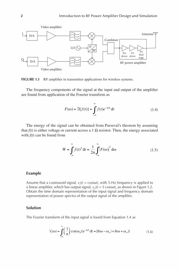
Radio frequency (RF) amplifiers are critical components and are widely used in applications including communication systems, radar applications, semiconductor manufacturing, magnetic resonance imaging (MRI), and induction heating. Use of RF amplifier as a core element in conjunction with an antenna in transmitter applica-tions for wireless communication systems is illustrated in Figure 1.1.
The frequency of operation for the amplifiers is based on the application and varies from the very low frequency range to microwave frequencies. In any type of application, when a signal needs to be amplified to a certain level at the frequency of interest, the amplification process of the signal is accomplished using RF power amplifiers (PAs). The power level of the amplifiers also varies, and it can be anywhere from milliwatt to megawatt ranges. The commonly used RF amplifier topologies are A, B, AB, C, D, E, F, and S class. These topologies represent linear or nonlinear amplification of the signal. Linear amplification is realized by using class A, B, or AB amplifier topologies, whereas nonlinear amplification is performed with class C, D, E, F, and S amplifiers. Class D, E, F, and S amplifiers are known as switch-mode amplifiers where the active device or transistor is used as a switch during the opera-tion of the amplifier. The relation between the RF signal waveforms at the input and output of the linear amplifiers can be expressed with the following relation:
vo(t) = βvi(t) (1.1)
When the amplifier is operating in nonlinear mode, then the signals at the input and output are expressed using the power series, as given in Equation 1.2:
v t v t v t v to i i i( ) ( ) ( ) ( )= + + + +α α α α0 1 22
33 … (1.2)
Equation 1.2 represents weak nonlinearities in the amplifier response. When weak distortion takes place, harmonics disappear as the signal amplitude gets smaller. Coefficients in Equation 1.2 can be found from
αn
no
in
i
==
1
0nd v t
dv tv
!( )
( ) (1.3)
2 Introduction to RF Power Amplifier Design and Simulation
The frequency components of the signal at the input and output of the amplifier are found from application of the Fourier transform as
F f t f t e t( ) ( ) ( )ω ω= ℑ = −
−∞
∞
∫ j t d (1.4)
The energy of the signal can be obtained from Parseval’s theorem by assuming that f(t) is either voltage or current across a 1 Ω resistor. Then, the energy associated with f(t) can be found from
W f t t F= =−∞
∞
−∞
∞
∫ ∫( ) ( )2 212
d dπ
ω ω (1.5)
Example
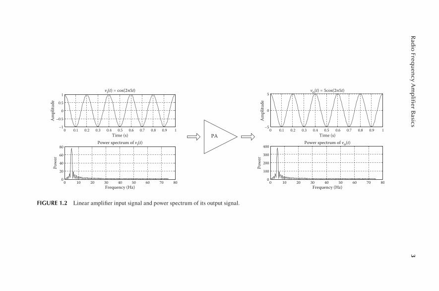
Assume that a cosinusoid signal, vi(t) = cos(ωt), with 5-Hz frequency is applied to a linear amplifier, which has output signal, vo(t) = 5 cos(ωt), as shown in Figure 1.2. Obtain the time domain representation of the input signal and frequency domain representation of power spectra of the output signal of the amplifier.
Solution
The Fourier transform of the input signal is found from Equation 1.4 as
V t tij t
o od( ) cos( ) [ ( ) ( )]ωπ
ω δ ω ω δ ω ωω=
= − + +−1o e
−−∞
∞
∫ (1.6)
D/A
D/A
I
Q
Video amplifier
Video amplifier
LO 0°90°
Combiner
Predriver
PAdriver
PAfinalstage
Antenna
RF power amplifier
FIGURE 1.1 RF amplifier in transmitter applications for wireless systems.
3R
adio
Frequ
ency A
mp
lifier B
asics
0 0.1 0.2 0.3 0.4 0.5 0.6 0.7 0.8 0.9 1–1
–0.5
0
0.5
1vi(t) = cos(2π5t)
Time (s)
Am
plitu
de
0 10 20 30 40 50 60 70 800
20
40
60
80Power spectrum of vi(t)
Frequency (Hz)
0 0.1 0.2 0.3 0.4 0.5 0.6 0.7 0.8 0.9 1
vo(t) = 5cos(2π5t)
Time (s)
0 10 20 30 40 50 60 70 80
Power spectrum of vo(t)
Frequency (Hz)
Pow
er
Am
plitu
dePo
wer
–5
0
5
0
100
200
300
400
PA
FIGURE 1.2 Linear amplifier input signal and power spectrum of its output signal.
4 Introduction to RF Power Amplifier Design and Simulation
and the output
V t tjo o o od( ) cos( ) [ ( ) ( )ω
πω δ ω ω δ ω ωω=
= − + +−55e t ]]
−∞
∞
∫ (1.7)
The power spectra of the output signal are obtained with application of Equation 1.5. The input signal and power spectrum of the output signal are illus-trated in frequency and time domain in Figure 1.2.
In the amplifier design, there are several parameters that indicate the perfor-mance of the amplifier: amplifier gain, output power, stability, linearity, DC supply voltage, efficiency, and ruggedness. The thermal profile of individual transistors and the overall amplifier are also very important to prevent the catastrophic failure of an amplifier.
The basic RF amplifier is illustrated in Figure 1.3. The amplifier mode of opera-tion depends on how the metal–oxide–semiconductor field-effect transistor (MOSFET) is biased based on the voltages applied from gate to source, Vgs, and from drain to source, Vds. The MOSFET can be operated either as a dependent current source or as a switch. When it operates as a dependent current source, the ohmic (linear) region becomes the operational region for the MOSFET.
The saturation (active) region is the operational region for the MOSFET when it is operating as a switch. As a result, the operational region of the active device such as the MOSFET shown in Figure 1.3 determines the amplifier mode with vari-able parameters such as Vgs and Vds.
In practice, RF PAs are implemented as part of systems that include several sub-assemblies such as DC power supply unit for amplifier, line filter, housekeeping power supply, system controller, splitter, combiner, coupler, compensator, and PA modules, as illustrated in Figure 1.4. Several PA modules are combined to obtain higher power levels via combiners. Couplers are used to monitor the reflected and forward power and provide control signal to the system controller. The system controller then adjusts the level of RF input signal to deliver the desired amount of output power.
VDC
RF choke
Load
Inputmatchingnetwork
Outputmatchingnetwork
RFin
FIGURE 1.3 Basic RF amplifier.
5Radio Frequency Amplifier Basics
1.2 RF AMPLIFIER TERMINOLOGY
In this section, some of the common terminologies used in RF PA design will be discussed. For this discussion, consider the simplified RF PA block diagram given in Figure 1.5. In the figure, RF PA is simply considered as a three-port network, where the RF input signal port, the DC input port, and the RF signal output port constitute the ports of the network as illustrated. Power that is not converted to RF output power, Pout, is dissipated as heat and designated by Pdiss, as shown in Figure 1.5. The dissipated power, Pdiss, is found from
Pdiss = (Pin + PDC) − Pout (1.8)
1.2.1 Gain
RF PA gain is defined as the ratio of the output power to the input power, as given by
GPP
= out
in
(1.9)
Daisy chain
Line filter
PA module
Driv
er
PSU module
PSU moduleFilter
ree-phase AC in
HK supply
brkr
SystemcontrollerCustomer
interface
Interlock Powersupply
controllerCombiner
filtercoupler RF output
Daisy chainCompensator
V IPA module
Driv
er
Daisychain
FIGURE 1.4 Typical RF amplifier system architecture.
PA
PDC
Pin( fo) Pout( fo)
Pdiss( fo)
Load
FIGURE 1.5 RF PA as a three-port network.
6 Introduction to RF Power Amplifier Design and Simulation
It can be defined in terms of decibels as
GPP
( ) log [ ]dB dBout
in
= 10 (1.10)
RF PA amplifier gain is higher at lower frequencies. This can be illustrated based on the measured data for a switched-mode RF amplifier operating at high-frequency (HF) range in Figure 1.6 for several applied DC supply voltages.
It is possible to obtain higher gain level when multiple amplifiers are cascaded to obtain multistage amplifier configuration, as shown in Figure 1.7.
The overall gain of the multistage amplifier system for the one shown in Figure 1.7 can then be found from
G G G Gtot PA PA PAdB dB dB dB( ) ( ) ( ) ( )= + +1 2 3 (1.11)
The unit of the gain is given in terms of decibels because it is the ratio of the output power to the input power. It is important to note that decibel is not a unit that defines the power. In amplifier terminology, dBm is used to define the power. dBm is found from
dBmmW
= 101
logP
(1.12)
141210
8642012.5 13 13.5
Gain at VDC = 60 VGain at VDC = 80 VGain at VDC = 100 VGain at VDC = 120 V
Frequency (MHz)
Gai
n (d
B)
14 14.5
FIGURE 1.6 Measured gain variation vs. frequency for a switched-mode RF amplifier.
PA1GPA1 (dB)
PA2GPA2 (dB)
PA3GPA3 (dB)
PoutPin
FIGURE 1.7 Multistage RF amplifiers.

7Radio Frequency Amplifier Basics
Example
In the RF system shown in Figure 1.8, the RF signal source can provide power out-put from 0 to 30 dBm. The RF signal is fed through a 1-dB T-pad attenuator and a 20-dB directional coupler where the sample of the RF signal is further attenuated by a 3-dB π-pad attenuator before power meter reading in dB. The “through” port of the directional coupler has 0.1 dB of loss before it is sent to PA. RF PA output is then connected to a 6-dB π-pad attenuator. If the power meter is reading 10 dBm, what is the power delivered to the load shown in Figure 1.8 in mW?
Solution
We need to find the power source first. The loss from the power meter to the RF signal source is
loss from power meter to source = 3 dB + 20 dB + 1 dB = 23 dB
Then, the power at the source is
RF source signal = 23 dBm + 10 dBm = 33 dBm
The total loss toward PA is due to the T-pad attenuator (1 dB) and the direc-tional coupler (0.1 dB) = 1.1 dB. So the transmitted RF signal at PA is
RF signal at PA = 33 dBm − 1.1 dBm = 31.9 dBm
Hence, the power delivered to the load is found from
power delivered to the load = 31.9 dBm – 6 dBm = 25.9 dBm
Power delivered in mW is found from
P( ) . [ ].
mW mWdBm
= = =10 10 389 041025 910
PRFin (0–35 dBm)
Directionalcoupler(20 dB)
PA
Power meter
Reading = 10 dBm
T-Pad (1 dB) IL = 0.1 dB π-Pad (6 dB)
π-Pa
d (3
dB)
Load
FIGURE 1.8 RF system with coupler and attenuation pads.
8 Introduction to RF Power Amplifier Design and Simulation
1.2.2 EfficiEncy
In practical applications, RF PA is implemented as a subsystem and consumes most of the DC power from the supply. As a result, minimal DC power consumption for the amplifier becomes important and can be accomplished by having high RF PA efficiency. RF PA efficiency is one of the critical and most important amplifier per-formance parameters. Amplifier efficiency can be used to define the drain efficiency for MOSFET or collector efficiency for a bipolar junction transistor (BJT). Amplifier efficiency is defined as the ratio of the RF output power to power supplied by the DC source and can be expressed as
η(%) = ×PPout
DC
100 (1.13)
Efficiency in terms of gain can be put in the following form:
η(%) =
+
−
×1
11
100PP Gdiss
out
(1.14)
The maximum efficiency is possible when there is no dissipation, i.e., Pdiss = 0. The maximum efficiency from Equation 1.14 is then equal to
η(%) =
−
×1
11
100
G
(1.15)
When RF input power is included in the efficiency calculation, the efficiency is then called as power-added efficiency, ηPAE, and found from
ηPAEout in
DC
(%) =−
×P PP
100 (1.16)
or
η ηPAE(%) = −
×1
1100
G (1.17)
Example
RF PA delivers 200[W] to a given load. If the input supply power for this ampli-fier is given to be 240[W], and the power gain of the amplifier is 15 dB, find the (a) drain efficiency and (b) power-added efficiency.
9Radio Frequency Amplifier Basics
Solution
a. The drain efficiency is found from Equation 1.13 as
η(%) . %= × = × =PPout
DC
100200240
100 83 33
b. Power-added efficiency is found from Equation 1.17 as
η ηPAE(%) . %= −
× = −
=1
1100 83 1
115
77 47G
1.2.3 PowEr outPut caPability
The power output capability of an amplifier is defined as the ratio of the output power for the amplifier to the maximum values of the voltage and current that the device experiences during the operation of the amplifier. When there are more than one transistor, or the number of the transistors increases due to amplifier configura-tion used in such push–pull configuration or any other combining techniques, this is reflected in the denominator of the following equation:
cPVpo
NI=
max max
(1.18)
1.2.4 linEarity
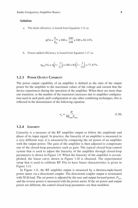
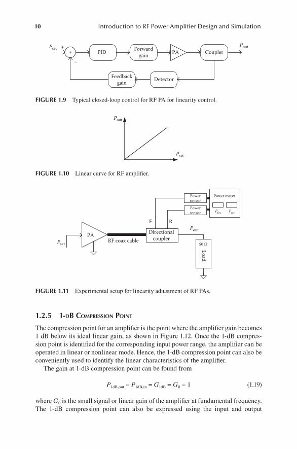
Linearity is a measure of the RF amplifier output to follow the amplitude and phase of its input signal. In practice, the linearity of an amplifier is measured in a very different way; it is measured by comparing the set power of an amplifier with the output power. The gain of the amplifier is then adjusted to compensate one of the closed-loop parameters such as gain. The typical closed-loop control system that is used to adjust the linearity of the amplifier through closed-loop parameters is shown in Figure 1.9. When the linearity of the amplifier is accom-plished, the linear curve shown in Figure 1.10 is obtained. The experimental setup that is used to calibrate RF PAs to have linear characteristics is given in Figure 1.11.
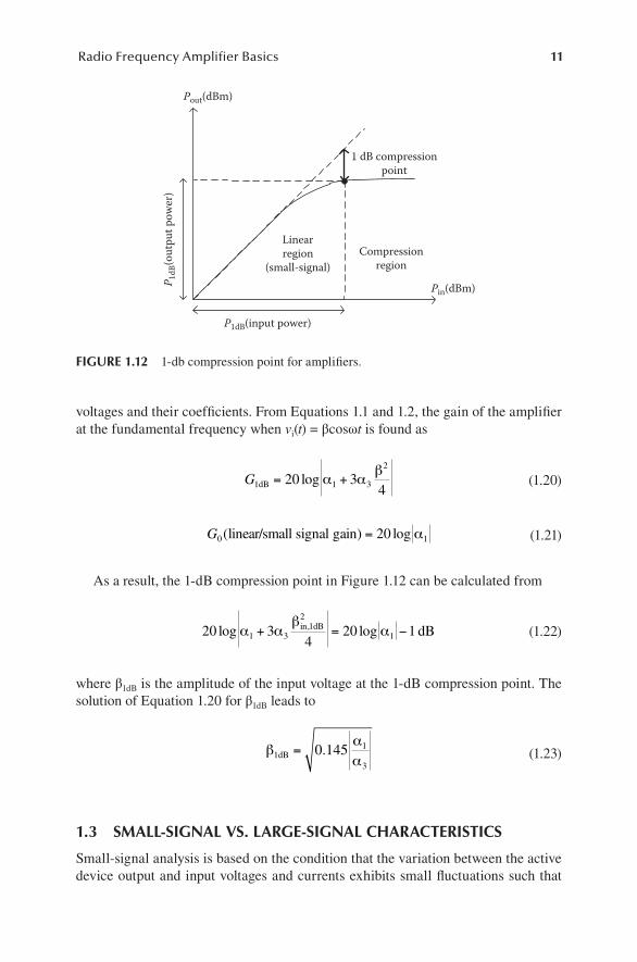
In Figure 1.11, the RF amplifier output is measured by a thermocouple-based power meter via a directional coupler. The directional coupler output is terminated with 50 Ω load. The set power is adjusted by the user and output forward power, Pfwr, and the reverse power is measured with the power meter. If the set power and output power are different, the control closed-loop parameters are then modified.
10 Introduction to RF Power Amplifier Design and Simulation
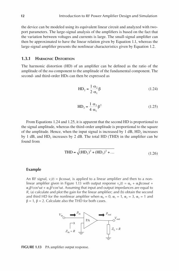
1.2.5 1-db comPrEssion Point
The compression point for an amplifier is the point where the amplifier gain becomes 1 dB below its ideal linear gain, as shown in Figure 1.12. Once the 1-dB compres-sion point is identified for the corresponding input power range, the amplifier can be operated in linear or nonlinear mode. Hence, the 1-dB compression point can also be conveniently used to identify the linear characteristics of the amplifier.
The gain at 1-dB compression point can be found from
P1dB,out − P1dB,in = G1dB = G0 − 1 (1.19)
where G0 is the small signal or linear gain of the amplifier at fundamental frequency. The 1-dB compression point can also be expressed using the input and output
+ PID Forwardgain PA Coupler
DetectorFeedbackgain
PoutPset +
–
FIGURE 1.9 Typical closed-loop control for RF PA for linearity control.
Pout
Pset
FIGURE 1.10 Linear curve for RF amplifier.
Pout
Pset
PARF coax cable
Directionalcoupler
F
50 Ω
Power meterPowersensor
Pfwr PrevPowersensor
R
Load
FIGURE 1.11 Experimental setup for linearity adjustment of RF PAs.
11Radio Frequency Amplifier Basics
voltages and their coefficients. From Equations 1.1 and 1.2, the gain of the amplifier at the fundamental frequency when vi(t) = βcosωt is found as
G1 1 3
2
20 34dB = +log α αβ
(1.20)
G0 120( ) loglinear/small signal gain = α (1.21)
As a result, the 1-dB compression point in Figure 1.12 can be calculated from
20 34
20 11 31
2
1log log,α αβ
α+ = −in dB dB (1.22)
where β1dB is the amplitude of the input voltage at the 1-dB compression point. The solution of Equation 1.20 for β1dB leads to
βαα1
1
3
0 145dB = . (1.23)
1.3 SMALL-SIGNAL VS. LARGE-SIGNAL CHARACTERISTICS
Small-signal analysis is based on the condition that the variation between the active device output and input voltages and currents exhibits small fluctuations such that
Compressionregion
Linearregion
(small-signal)
1 dB compressionpoint
Pin(dBm)
Pout(dBm)
P1dB(input power)
P 1dB
(out
put p
ower
)
FIGURE 1.12 1-db compression point for amplifiers.
12 Introduction to RF Power Amplifier Design and Simulation
the device can be modeled using its equivalent linear circuit and analyzed with two-port parameters. The large-signal analysis of the amplifiers is based on the fact that the variation between voltages and currents is large. The small-signal amplifier can then be approximated to have the linear relation given by Equation 1.1, whereas the large-signal amplifier presents the nonlinear characteristics given by Equation 1.2.
1.3.1 Harmonic distortion
The harmonic distortion (HD) of an amplifier can be defined as the ratio of the amplitude of the nω component to the amplitude of the fundamental component. The second- and third-order HDs can then be expressed as
HD22
1
12
=αα
β (1.24)
HD33
1
214
=αα
β (1.25)
From Equations 1.24 and 1.25, it is apparent that the second HD is proportional to the signal amplitude, whereas the third-order amplitude is proportional to the square of the amplitude. Hence, when the input signal is increased by 1 dB, HD2 increases by 1 dB, and HD3 increases by 2 dB. The total HD (THD) in the amplifier can be found from
THD HD HD= + +( ) ( )22
32 … (1.26)
Example
An RF signal, vi(t) = βcosωt, is applied to a linear amplifier and then to a non-linear amplifier given in Figure 1.13 with output response vo(t) = α0 + α1βcosωt + α2β2cos2ωt + α3β3cos3ωt. Assuming that input and output impedances are equal to R, (a) calculate and plot the gain for the linear amplifier; and (b) obtain the second and third HD for the nonlinear amplifier when α0 = 0, α1 = 1, α2 = 3, α3 = 1 and β = 1, β = 2. Calculate also the THD for both cases.
Zin = R ZL = R
Vin
PA
Pin PoutVout
FIGURE 1.13 PA amplifier output response.
13Radio Frequency Amplifier Basics
Solution
a. For linear amplifier characteristics, the output voltage is expressed using Equation 1.1 as
vo(t) = βvi(t) (1.27)
which can also be written as
12
12
2 2 2
Rv t
Rv to i( ) ( )= β (1.28)
or
Po = β2Pi (1.29)
When power (Equation 1.21) is given in dBm, then Equation 1.21 can be expressed as
10 10 2log logP Po i
1 mW 1 mW
=
β (1.30)
or
Po(dBm) = 10log(β2) + Pin(dBm) (1.31)
Then, the power gain is obtained from Equation 1.24 as
Gain(dBm) = G(dBm) = 10log(β2) = Po(dBm) − Pin(dBm) (1.32)
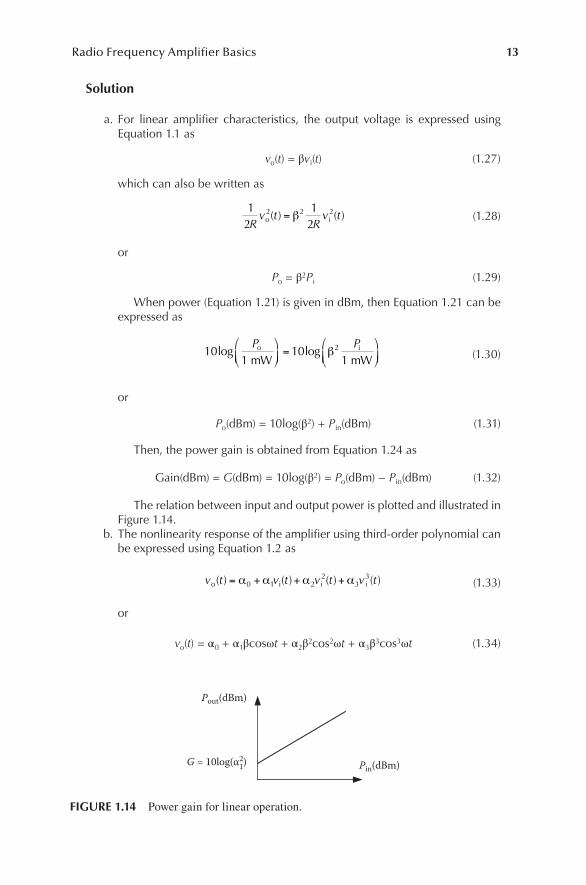
The relation between input and output power is plotted and illustrated in Figure 1.14.
b. The nonlinearity response of the amplifier using third-order polynomial can be expressed using Equation 1.2 as
v t v t v t v to( ) ( ) ( ) ( )= + + +α α α α0 1 22
33
i i i (1.33)
or
vo(t) = α0 + α1βcosωt + α2β2cos2ωt + α3β3cos3ωt (1.34)
Pin(dBm)
Pout(dBm)
G = 10log(α12)
FIGURE 1.14 Power gain for linear operation.
14 Introduction to RF Power Amplifier Design and Simulation
As seen from Equation 1.24, we have fundamental, second-order harmonic, third-order harmonic, and a DC component in the output response of the ampli-fier. In Equation 1.27, it is also seen that the DC component exists due to the second harmonic content. Equation 1.28 can be rearranged to give the following closed-form relation:
v t t t to( ) cos cos cos= + + + +α α β ωα β α β
ωα β
ω0 12
22
23
3
2 22 3
4++α β
ω33
43cos t (1.35)
which can be simplified to
v t to( ) cos= +
+ +
+
α
α βα
α ββ ω
α0
22
13
22
23
4 2 +β ω
α βω2 3
3
24
3cos cost t (1.36)
When α1 = 1, α2 = 3, α3 = 1 and β = 1, HD2 and HD3 are obtained from Equations 1.24 and 1.25 as
HD22
1
12
12311 1 5= = =
αα
β ( ) . (1.37)
HD33
1
2 214
14111 0 25= = =
αα
β ( ) . (1.38)
When α1 = 1, α2 = 3, α3 = 1 and β = 2,
HD22
1
12
12312 3= = =
αα
β ( ) (1.39)
HD33
1
2 214
14112 1= = =
αα
β ( ) (1.40)
The THD for this system is found from Equation 1.26 as
THD = + =( . ) ( . ) .1 5 0 25 1 56252 2 (1.41)
and
THD = + =( ) ( ) .3 1 3 162 2 (1.42)
Example
The input of voltage for an RF circuit is given to be vin(t) = βcos(ωt). The RF circuit generates signal at the third harmonic as V3cos(3ωt). What is the 1-dB compres-sion point?

15Radio Frequency Amplifier Basics
Solution
Using Equation 1.36, the amplitude of the third harmonic component can be found from
α β
αβ
33
3 3334
4= =V
Vor (1.43)
Then, the 1-dB compression point, β1dB, is found from Equation 1.23 as
βαα
β α β α1
1
3
31
3
31
3
0 1450 1454
0 19dB = = =..
.V V (1.44)
1.3.2 intErmodulation
When a signal composed of two cosine waveforms with different frequencies
vi(t) = β1cosω1t + β2cosω2t (1.45)
is applied to an input of an amplifier, the output signal consists of components of the self-frequencies and their products created by frequencies by ω1 and ω2 given by the following equation:
vo(t) = α1(β1cosω1t + β2cosω2t) + α2(β1cosω1t + β2cosω2t)2
+ α3(β1cosω1t + β2cosω2t)3 (1.46)
or
v t t t
t
o ( ) ( cos cos )
( cos )
= + +
+ +
α β ω β ω α
β ω
1 1 1 2 2 2
12
1
12
1 2112
1 2
12
22
2
1 2 1 2 1 2
β ω
β β ω ω ω ω
( cos )
(cos( ) cos( )
+
+ + + −
t
t tt
t t
)
(cos ) (cos )
+
+
α
β ω β β ω
3
13
1 1 22
1
34
32
++ + −
+
14
334
2
34
13
1 1 22
1 2
12
2
β ω β β ω ω
β β
cos( ) (cos( ) )
(
t t
ccos( ) ) (cos ) (cos )232
34
141 2 1
22 2 2
32ω ω β β ω β ω− + + +t t t ββ ω
β β ω ω β β
23
2
12
2 1 2 1 22
3
34
234
(cos )
(cos( ) ) (cos
t
t+ + + (( ) )ω ω1 22+
t
(1.47)
16 Introduction to RF Power Amplifier Design and Simulation
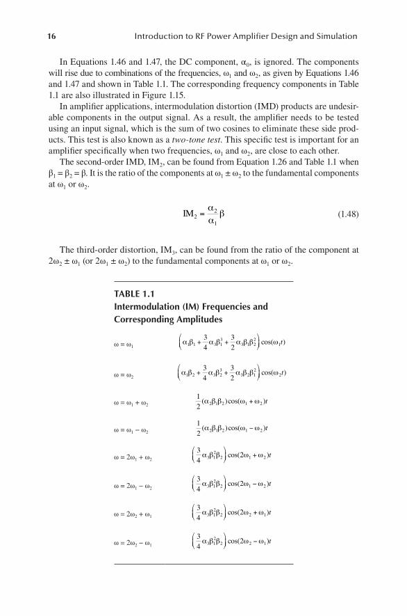
In Equations 1.46 and 1.47, the DC component, α0, is ignored. The components will rise due to combinations of the frequencies, ω1 and ω2, as given by Equations 1.46 and 1.47 and shown in Table 1.1. The corresponding frequency components in Table 1.1 are also illustrated in Figure 1.15.
In amplifier applications, intermodulation distortion (IMD) products are undesir-able components in the output signal. As a result, the amplifier needs to be tested using an input signal, which is the sum of two cosines to eliminate these side prod-ucts. This test is also known as a two-tone test. This specific test is important for an amplifier specifically when two frequencies, ω1 and ω2, are close to each other.
The second-order IMD, IM2, can be found from Equation 1.26 and Table 1.1 when β1 = β2 = β. It is the ratio of the components at ω1 ± ω2 to the fundamental components at ω1 or ω2.
IM22
1
=αα
β (1.48)
The third-order distortion, IM3, can be found from the ratio of the component at 2ω2 ± ω1 (or 2ω1 ± ω2) to the fundamental components at ω1 or ω2.
TABLE 1.1Intermodulation (IM) Frequencies and Corresponding Amplitudes
ω = ω1α β α β α β β ω1 1 3 1
33 1 2
21
34
32
+ +
cos( )t
ω = ω2α β α β α β β ω1 2 3 2
33 2 1
22
34
32
+ +
cos( )t
ω = ω1 + ω2
12 2 1 2 1 2( )cos( )α β β ω ω+ t
ω = ω1 − ω2
12 2 1 2 1 2( )cos( )α β β ω ω− t
ω = 2ω1 + ω2
34
23 12
2 1 2α β β ω ω
+cos( )t
ω = 2ω1 − ω2
34
23 12
2 1 2α β β ω ω
−cos( )t
ω = 2ω2 + ω1
34
23 12
2 2 1α β β ω ω
+cos( )t
ω = 2ω2 − ω1
34
23 12
2 2 1α β β ω ω
−cos( )t
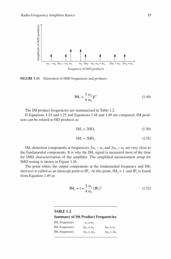
17Radio Frequency Amplifier Basics
IM33
1
234
=αα
β (1.49)
The IM product frequencies are summarized in Table 1.2.If Equations 1.24 and 1.25 and Equations 1.48 and 1.49 are compared, IM prod-
ucts can be related to HD products as
IM2 = 2HD2 (1.50)
IM3 = 3HD3 (1.51)
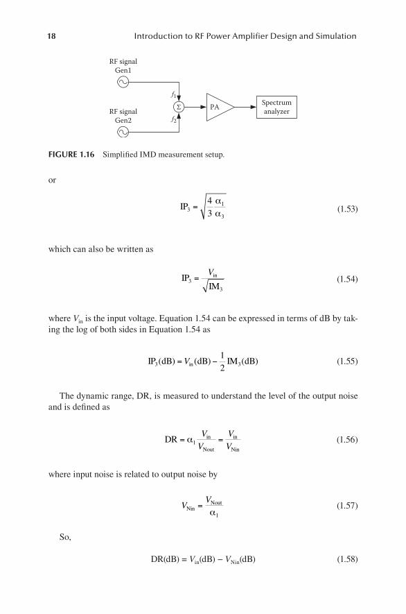
IM3 distortion components at frequencies 2ω1 − ω2 and 2ω2 − ω1 are very close to the fundamental components. It is why the IM3 signal is measured most of the time for IMD characterization of the amplifier. The simplified measurement setup for IMD testing is shown in Figure 1.16.
The point where the output components at the fundamental frequency and IM3 intersect is called as an intercept point or IP3. At this point, IM3 = 1, and IP3 is found from Equation 1.49 as
IM IP33
13
2134
= =αα
( ) (1.52)
Am
plitu
de o
f IM
D p
rodu
cts
ω1 – ω2 ω1 + ω22ω1 – ω2 2ω2 – ω1 2ω1 + ω2 2ω2 + ω1ω1 ω2
Frequency of IMD products
FIGURE 1.15 Illustration of IMD frequencies and products.
TABLE 1.2Summary of IM Product FrequenciesIM2 frequencies ω1 ± ω2
IM3 frequencies 2ω1 ± ω2 2ω2 ± ω1
IM5 frequencies 3ω1 ± 2ω1 3ω2 ± 2ω1
18 Introduction to RF Power Amplifier Design and Simulation
or
IP31
3
43
=αα (1.53)
which can also be written as
IPIMin
3
3
=V
(1.54)
where Vin is the input voltage. Equation 1.54 can be expressed in terms of dB by tak-ing the log of both sides in Equation 1.54 as
IP dB dB IM dBin3 312
( ) ( ) ( )= −V (1.55)
The dynamic range, DR, is measured to understand the level of the output noise and is defined as
DR in
Nout
in
Nin
= =α1VV
VV
(1.56)
where input noise is related to output noise by
VV
NinNout=α1
(1.57)
So,
DR(dB) = Vin(dB) − VNin(dB) (1.58)
RF signalGen1
RF signalGen2
f1
f2
Σ PA Spectrumanalyzer
FIGURE 1.16 Simplified IMD measurement setup.
19Radio Frequency Amplifier Basics
Intermodulation free dynamic range, IMFDR3, is defined as the largest DR pos-sible with no IM3 product. For the third-order IMD, VNout is defined by
V VNout in=34 3
3α (1.59)
We can obtain
V Vin Nout=4
3 3
3α (1.60)
Substitution of Equation 1.59 into Equation 1.56 gives IMFDR3 as
DR IMFDR in
Noutin
Nout
= = = =3 113
32
343
1α
αα
VV
VV (1.61)
Since VNout = α1 VNin from Equation 1.54, Equation 1.56 can be written in terms of input noise as
IMFDR in
Noutin
Nin3 1
1
32
343
1= = =α
αα
VV
VV (1.62)
When Equations 1.53 and 1.62 are compared, IMFDR3 can also be expressed using IP3 as
IMFDRIP
Nin3
3
23
=V
(1.63)
or in terms of dB, Equation 1.63 can also be given by
IMFDR dB IP dB dBNin3 323
( ) ( ( ) ( ))= −V (1.64)
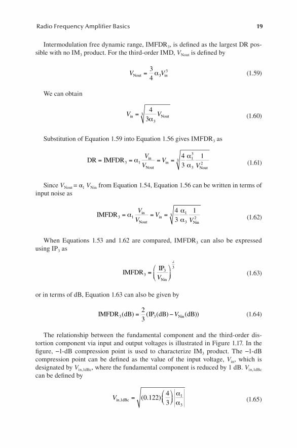
The relationship between the fundamental component and the third-order dis-tortion component via input and output voltages is illustrated in Figure 1.17. In the figure, −1-dB compression point is used to characterize IM3 product. The −1-dB compression point can be defined as the value of the input voltage, Vin, which is designated by Vin,1dBc, where the fundamental component is reduced by 1 dB. Vin,1dBc can be defined by
Vin dBc, ( . )11
3
0 12243
=
αα (1.65)
20 Introduction to RF Power Amplifier Design and Simulation
which is also equal to
Vin dBc IP, ( . )1 30 122= (1.66)
Equation 1.66 can be expressed in dB as
Vin,1dBc(dB) = IP3(dB) − 9.64 dB (1.67)
As a result, once IP3 is determined, Equation 1.66 can be used to calculate the −1-dB compression point for the amplifier.
Example
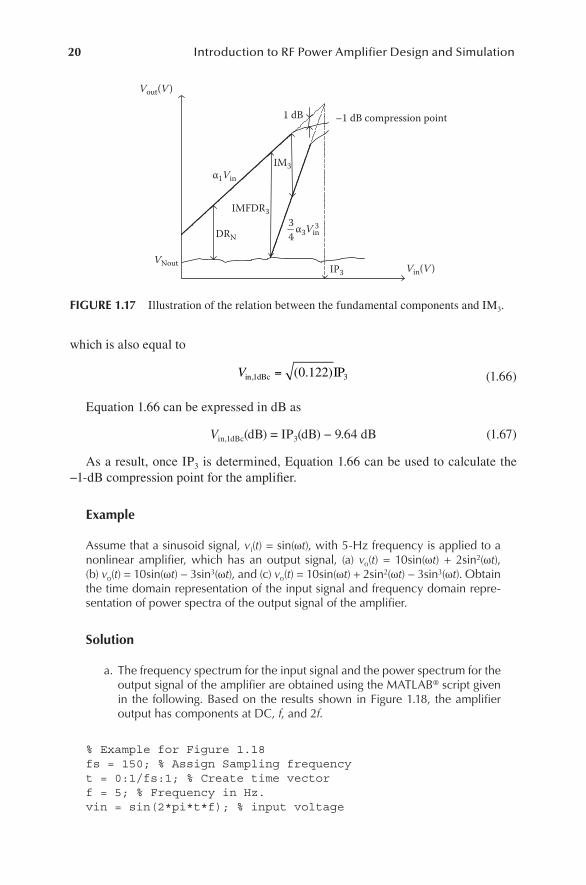
Assume that a sinusoid signal, vi(t) = sin(ωt), with 5-Hz frequency is applied to a nonlinear amplifier, which has an output signal, (a) vo(t) = 10sin(ωt) + 2sin2(ωt), (b) vo(t) = 10sin(ωt) − 3sin3(ωt), and (c) vo(t) = 10sin(ωt) + 2sin2(ωt) − 3sin3(ωt). Obtain the time domain representation of the input signal and frequency domain repre-sentation of power spectra of the output signal of the amplifier.
Solution
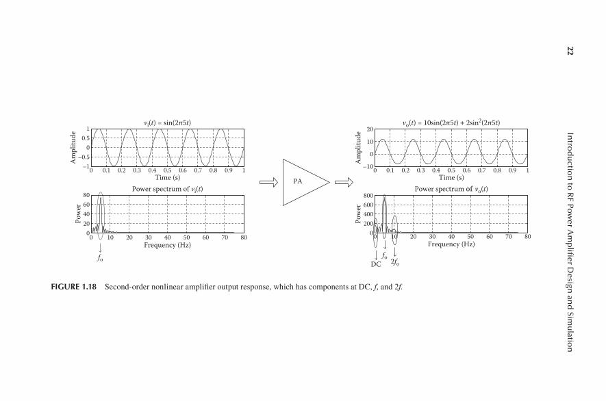
a. The frequency spectrum for the input signal and the power spectrum for the output signal of the amplifier are obtained using the MATLAB® script given in the following. Based on the results shown in Figure 1.18, the amplifier output has components at DC, f, and 2f.
% Example for Figure 1.18fs = 150; % Assign Sampling frequencyt = 0:1/fs:1; % Create time vectorf = 5; % Frequency in Hz.vin = sin(2*pi*t*f); % input voltage
IP3 Vin(V )
Vout(V )
VNout
1 dB
34
α3Vin3
α1Vin
DRN
IMFDR3
IM3
–1 dB compression point
FIGURE 1.17 Illustration of the relation between the fundamental components and IM3.

21Radio Frequency Amplifier Basics
vout = 10*sin(2*pi*t*f)+2*(sin(2*pi*t*f)).^2; % output voltage
lfft = 1024; % length of FFTVin = fft(vin,lfft);% Take FFTVin = Vin(1:lfft/2); % FFT is symmetric, dont need second
% halfVout = fft(vout,lfft);% Repeat it for output
Vout = Vout(1:lfft/2);magvin = abs(Vin); % Magnitude of FFT of vinmagvout = abs(Vout);% Magnitude of FFT of voutf = (0:lfft/2-1)*fs/lfft; % Create frequency vectorfigure(1) % Plotting begins subplot(2,1,1)plot(t,vin);title('v_i(t) = sin(2\pi5t)','fontsize',12)xlabel('Time (s)');ylabel('Amplitude');grid onsubplot(2,1,2)plot(f,magvin);title('Power Spectrum of v_i(t)','fontsize',12);xlabel('Frequency (Hz)');ylabel('Power');grid on
% Obtain the Output Waveforms
figure(2)subplot(2,1,1)plot(t,vout);title('v_o(t) = 10sin(2\pi5t)+2sin^2(2\pi5t)',
'fontsize',12)xlabel('Time (s)');ylabel('Amplitude');grid onsubplot(2,1,2)plot(f,magvout);title('Power Spectrum of v_o(t)','fontsize',12);xlabel('Frequency (Hz)');ylabel('Power');grid on
b. The MATLAB script in part (a) is modified for input and output voltage to obtain the third-order response shown in Figure 1.19. As seen from Figure 1.19, the output signal does not have a DC component anymore. The third-order effect shows itself as clipping in the time domain signal and funda-mental and third-order components at the output power spectra of the signal.
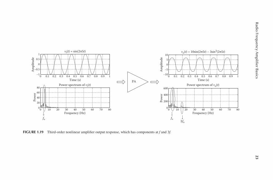
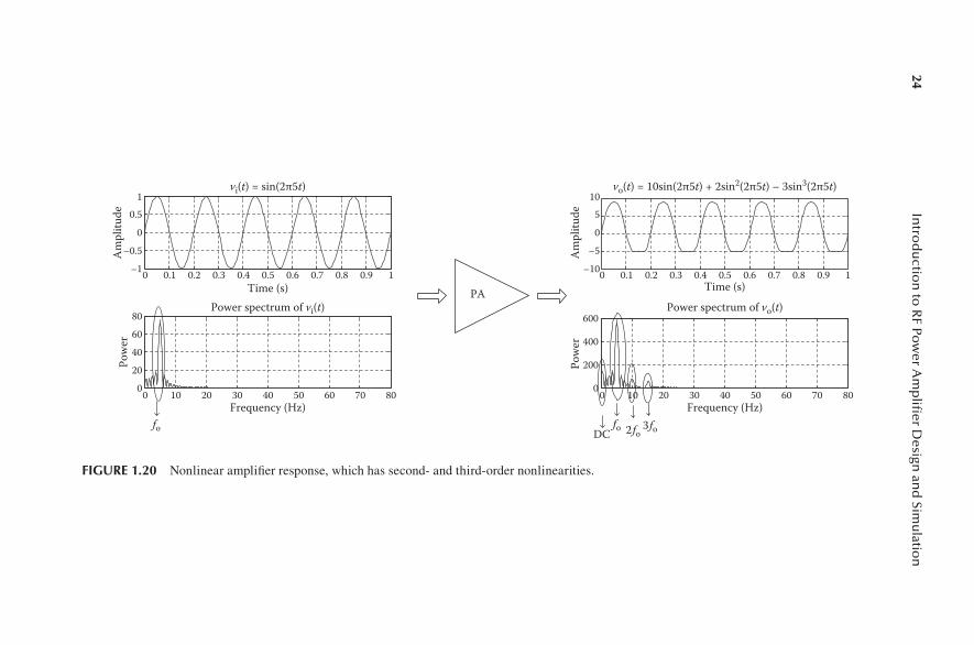
c. Using the modified MATLAB script in parts (a) and (b), the time domain and frequency domain signals are obtained and illustrated in Figure 1.20.
22In
trod
uctio
n to
RF Po
wer A
mp
lifier D
esign an
d Sim
ulatio
n
PA0 0.1 0.2 0.3 0.4 0.5 0.6 0.7 0.8 0.9 1–1
–0.50
0.51
Time (s)0 0.1 0.2 0.3 0.4 0.5 0.6 0.7 0.8 0.9 1
Time (s)
Frequency (Hz)
Am
plitu
de
0 10 20 30 40 50 60 70 80Frequency (Hz)
0 10 20 30 40 50 60 70 80020406080
Pow
er
–10
0
10
20
Am
plitu
de
0200400600800
Pow
er
fo fo 2foDC
vi(t) = sin(2π5t) vo(t) = 10sin(2π5t) + 2sin2(2π5t)
Power spectrum of vi(t) Power spectrum of vo(t)
FIGURE 1.18 Second-order nonlinear amplifier output response, which has components at DC, f, and 2f.
23R
adio
Frequ
ency A
mp
lifier B
asics
PA
–1
–0.5
0
0.51
Am
plitu
de
0
20
40
6080
Pow
er
Am
plitu
dePo
wer
–10–5
05
10
0
200
400
600
0 0.1 0.2 0.3 0.4 0.5 0.6 0.7 0.8 0.9 1Time (s)
0 0.1 0.2 0.3 0.4 0.5 0.6 0.7 0.8 0.9 1Time (s)
vi(t) = sin(2π5t)
Frequency (Hz)0 10 20 30 40 50 60 70 80
Frequency (Hz)0 10 20 30 40 50 60 70 80
Power spectrum of vi(t)
vo(t) = 10sin(2π5t) − 3sin3(2π5t)
Power spectrum of vo(t)
fo fo3fo
FIGURE 1.19 Third-order nonlinear amplifier output response, which has components at f and 3f.
24In
trod
uctio
n to
RF Po
wer A
mp
lifier D
esign an
d Sim
ulatio
n
PA
–1
–0.5
0
0.51
Am
plitu
de
–10
–5
0
510
Am
plitu
de
0
20
40
60
80
Pow
er
0
200
400
600
Pow
er
0 0.1 0.2 0.3 0.4 0.5 0.6 0.7 0.8 0.9 1Time (s)
Frequency (Hz)0 10 20 30 40 50 60 70 80
vi(t) = sin(2π5t)
Power spectrum of vi(t)
0 0.1 0.2 0.3 0.4 0.5 0.6 0.7 0.8 0.9 1Time (s)
Frequency (Hz)0 10 20 30 40 50 60 70 80
vo(t) = 10sin(2π5t) + 2sin2(2π5t) – 3sin3(2π5t)
Power spectrum of vo(t)
fo fo 2fo 3foDC
FIGURE 1.20 Nonlinear amplifier response, which has second- and third-order nonlinearities.
25Radio Frequency Amplifier Basics
As illustrated, the output response has components at DC, f, 2f, and 3f. Overall, the level of the nonlinearity response of the amplifier strongly depends on the coefficients of the output signal.
1.4 RF AMPLIFIER CLASSIFICATIONS
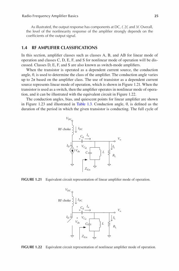
In this section, amplifier classes such as classes A, B, and AB for linear mode of operation and classes C, D, E, F, and S for nonlinear mode of operation will be dis-cussed. Classes D, E, F, and S are also known as switch-mode amplifiers.
When the transistor is operated as a dependent current source, the conduction angle, θ, is used to determine the class of the amplifier. The conduction angle varies up to 2π based on the amplifier class. The use of transistor as a dependent current source represents linear mode of operation, which is shown in Figure 1.21. When the transistor is used as a switch, then the amplifier operates in nonlinear mode of opera-tion, and it can be illustrated with the equivalent circuit in Figure 1.22.
The conduction angles, bias, and quiescent points for linear amplifier are shown in Figure 1.23 and illustrated in Table 1.3. Conduction angle, θ, is defined as the duration of the period in which the given transistor is conducting. The full cycle of
VDC
RF choke
+
+
ID
IDC
VdsRL
IL
IoVo
ZtLn
VCd
Cd
C L
FIGURE 1.21 Equivalent circuit representation of linear amplifier mode of operation.
VDC
RF choke
+
+ Vo
ILID
RL
Vds
Cd
VCd
Io
IDC
ZtLn
LC
FIGURE 1.22 Equivalent circuit representation of nonlinear amplifier mode of operation.
26 Introduction to RF Power Amplifier Design and Simulation
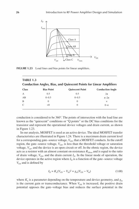
conduction is considered to be 360°. The points of intersection with the load line are known as the “quiescent” conditions or “Q points” or the DC bias conditions for the transistor and represent the operational device voltages and drain current, as shown in Figure 1.23.
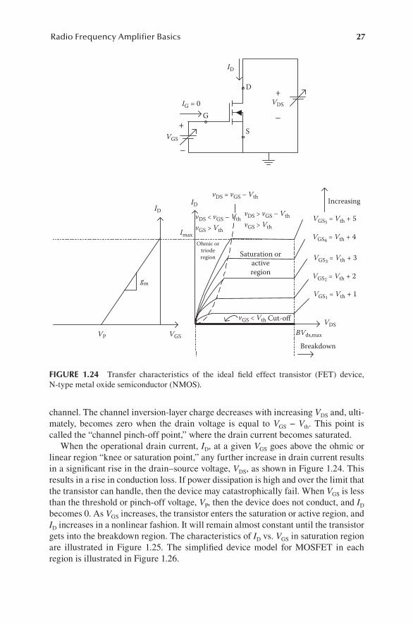
In our analysis, MOSFET is used as an active device. The ideal MOSFET transfer characteristics are illustrated in Figure 1.24. There is a maximum drain current level for a corresponding gate–source voltage, VGS, that a MOSFET conducts. In the cutoff region, the gate–source voltage, VGS, is less than the threshold voltage or saturation voltage, Vsat, and the device is an open circuit or off. In the ohmic region, the device acts as a resistor with an almost constant on-resistance RDSon and is equal to the ratio of drain voltage, VDS, and the drain current ID. In the linear mode of operation, the device operates in the active region where ID is a function of the gate–source voltage VGS and is defined by
ID = Kn(VGS − Vth)2 = gm(VGS − Vth) (1.68)
where Kn is a parameter depending on the temperature and device geometry, and gm is the current gain or transconductance. When VDS is increased, the positive drain potential opposes the gate–voltage bias and reduces the surface potential in the
VDSVmaxVsat
ID
Class A
Class AB
Class B
Imax
Class C
FIGURE 1.23 Load lines and bias points for linear amplifiers.
TABLE 1.3Conduction Angles, Bias, and Quiescent Points for Linear Amplifiers
Class Bias Point Quiescent Point Conduction Angle
A 0.5 0.5 2πAB 0–0.5 0–0.5 π–2πB 0 0 π
C <0 0 0–π
27Radio Frequency Amplifier Basics
channel. The channel inversion-layer charge decreases with increasing VDS and, ulti-mately, becomes zero when the drain voltage is equal to VGS − Vth. This point is called the “channel pinch-off point,” where the drain current becomes saturated.
When the operational drain current, ID, at a given VGS goes above the ohmic or linear region “knee or saturation point,” any further increase in drain current results in a significant rise in the drain–source voltage, VDS, as shown in Figure 1.24. This results in a rise in conduction loss. If power dissipation is high and over the limit that the transistor can handle, then the device may catastrophically fail. When VGS is less than the threshold or pinch-off voltage, VP, then the device does not conduct, and ID becomes 0. As VGS increases, the transistor enters the saturation or active region, and ID increases in a nonlinear fashion. It will remain almost constant until the transistor gets into the breakdown region. The characteristics of ID vs. VGS in saturation region are illustrated in Figure 1.25. The simplified device model for MOSFET in each region is illustrated in Figure 1.26.
Imax
BVds,max
vGS < Vth
VGS1 = Vth + 1
VGS2 = Vth + 2
VGS3 = Vth + 3
VGS4 = Vth + 4
VGS5 = Vth + 5
vDS = vGS – Vth Increasing
Ohmic ortrioderegion Saturation or
activeregion
BreakdownVGS
IDID
VDSVP
gm
G
D
S
Cut-off
vDS > vGS – VthvGS > Vth
vDS < vGS – VthvGS > Vth
VDS
VGS
ID
IG = 0+
–+
–
FIGURE 1.24 Transfer characteristics of the ideal field effect transistor (FET) device, N-type metal oxide semiconductor (NMOS).
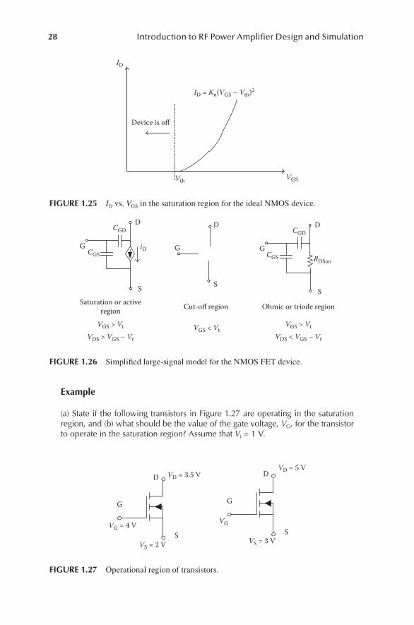
28 Introduction to RF Power Amplifier Design and Simulation
Example
(a) State if the following transistors in Figure 1.27 are operating in the saturation region, and (b) what should be the value of the gate voltage, VG, for the transistor to operate in the saturation region? Assume that Vt = 1 V.
Device is off
ID
ID = Kn(VGS – Vth)2
VGSVth
FIGURE 1.25 ID vs. VGS in the saturation region for the ideal NMOS device.
G
D
S
iD
CGD
CGSG
S
D
G
D
S
CGD
CGS RDSon
Ohmic or triode regionCut-off regionSaturation or activeregion
VGS > Vt VGS < VtVDS > VGS – Vt
VGS > Vt
VDS < VGS – Vt
FIGURE 1.26 Simplified large-signal model for the NMOS FET device.
D
G
S
VD = 3.5 V
VG = 4 V VG
VS = 3 V
D
G
S
VD = 5 V
VS = 2 V
FIGURE 1.27 Operational region of transistors.
29Radio Frequency Amplifier Basics
Solution
The condition to operate in the saturation region is
VGS > Vt
VDS > VGS − Vt
a. VGS = 4 − 2 = 2 [V] > Vt = 1 [V] and VDS = 3.5 − 2 = 1.5 [V] > VGS − Vt = 2 − 1 = 1 [V]. So, the first transistor is operating in the saturation region.
b. From the first condition, for the transistor to operate in the saturation region, VGS > 1 [V]. That requires gate voltage VG > 4 [V]. In addition, it is required that VGS < VDS + Vt = 2 + 1 = 3 [V]. The overall solution is
1 < VGS < 3
Since the source voltage is VS = 2 V, then,
1 < VG − 2 < 3 or 3 < VG < 5
1.4.1 convEntional amPlifiErs—classEs a, b, and c
In amplifier classes A, B, and C, the transistor can be modeled as the voltage-dependent current source and is shown in Figure 1.28. Most of the time, the class of these amplifiers is also known as conventional amplifiers.
The current iD flowing through the device, the drain-to-source voltage, and the voltage applied at the gate to source of the transistor in Figure 1.28 are
iD = IDC + Imcos(θ) (1.69)
VDC
RF choke
Cd
vds
+
+iD
IDC
VCd
vo
RL
io
C L
ZtLn
vGS iG
FIGURE 1.28 Conventional RF PA classes: classes A, B, and C.

30 Introduction to RF Power Amplifier Design and Simulation
vDS = VDC − Vmcos(θ) (1.70)
vGS = Vt + Vgsmcos(θ) (1.71)
where θ = ωt. The DC component of the drain current and the drain-to-source volt-age are equal to IDC and VDC, and the AC component is Im cos(θ), − Vm cos(θ) as given by
ID = IDC, VDS = VDC (1.72)
i I v VD DS m= = −mcos( ), cos( )θ θ (1.73)
Fourier integrals can be used to determine the DC power and output of the ampli-fier. The drain current, iD, can be represented using Fourier series expansion using sine or cosine functions, which are harmonically related as
i t I I n t I n tD o o( ) cos sin= + +=
∞
∑o an bn
n
ω ω1
(1.74)
v t V V n t V n tDS o o o( ) cos sin= + +=
∞
∑ an bn
n
ω ω1
(1.75)
The odd and even harmonic coefficients can be combined into a single cosine (or sine) to give
i t I I n tD o o( ) cos( )= + +=
∞
∑ n n
n
ω α1
(1.76)
v t V V n tDS o o( ) cos( )= + +=
∞
∑ n n
n
ω β1
(1.77)
where
I I In an bn= +2 2 (1.78)
31Radio Frequency Amplifier Basics
and
V V Vn an bn= +2 2 (1.79)
and
αnbn
an
=
−tan 1 I
I (1.80)
and
βnbn
an
=
−tan 1 V
V (1.81)
The impedance at the transistor load line of the transistor is found from
ZV e
I eZ etLn
j
j= =n
ntLn
j n
α
βφ
(1.82)
where ϕn = (αn − βn). The Fourier coefficients Io, Ian, and Ibn for the drain current are calculated from
IT
i t to D=−∫
1
2
2
( )/
/
dT
T
(1.83)
IT
i t k t tan =−∫
2
2
2
D o
T
T
d( )cos( )/
/
ω (1.84)
IT
i t k t tbn =−∫
2
2
2
D o
T
T
d( )sin( )/
/
ω (1.85)
where ωo = 2π/T. The fundamental component in Equation 1.82 is obtained when n = 1, and the DC components are found from Equation 1.83 as follows:
I I I Io DC m DCd= + =−∫
12π
θ θπ
π
( cos( )) (1.86)
32 Introduction to RF Power Amplifier Design and Simulation
I I I n I nan DC= + = =−∫
1π
θ θ θπ
π
( cos( ))cos( )m md when 1otherrwise Ian = 0 (1.87)
I I I n nbn = + =−∫
10
πθ θ θ
π
π
( cos( ))sin( )DC m d for all (1.88)
The same analysis and derivation can also be repeated for the drain-to-source voltage. Hence, the DC and the fundamental components of the drain current and the drain-to-source voltage at the resonant frequency, fo, are
I I V Vo DC o DC= =, (1.89)
I I V V1 1= =m, m (1.90)
DC power, PDC, from supply is then calculated from
PDC = VDCIDC (1.91)
The power delivered from the device to the output is represented by Po and cal-culated at the fundamental frequency, which is the resonant frequency of the LC network and is obtained from Equation 1.90 as
P V Io m m=12
(1.92)
The more general expression when operational frequency is not equal to resonant frequency for the output power can be found at the fundamental and harmonic fre-quencies as
P V I non = =12
1 2n n ncos( ), , ,φ … (1.93)
The transistor dissipation is calculated using
PT
v t i t tdiss DS D d= ∫1
0
( ) ( )
T
(1.94)
33Radio Frequency Amplifier Basics
which is also equal to
P P Pdiss DC o= −=
∞
∑ ,n
n 1
(1.95)
The drain efficiency is the ratio of the output power to DC supply power and cal-culated using Equations 1.91 and 1.93 as
η = =+
P
P
P
P Po
DC
o
diss o
, ,
,
n n
n
(1.96)
The maximum efficiency is obtained when
P Pdiss o+ ==
∞
∑ ,n
n 2
0
Then, the maximum efficiency from Equation 1.96 is found to be ηmax = 100%.The drive input power is calculated using Equation 1.71 for gate-to-source volt-
age, vGS, and gate current, iG, from
PT
v t i t tG GS G
T
d= ∫1
0
( ) ( ) (1.97)
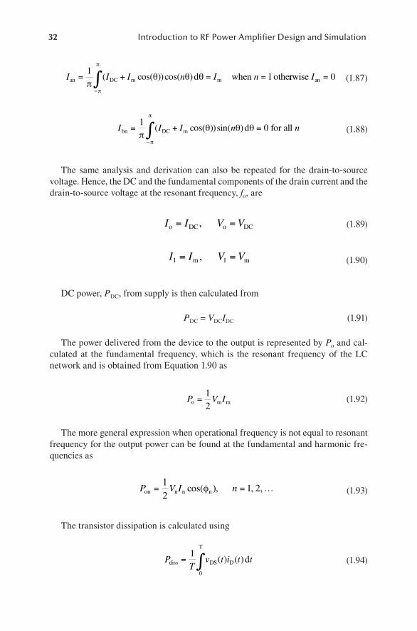
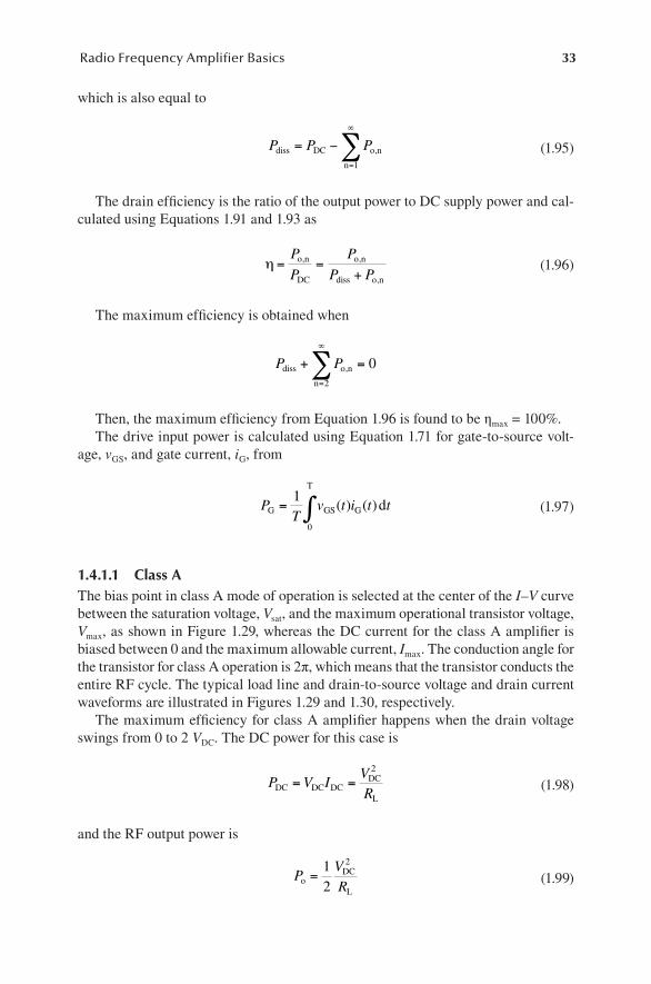
1.4.1.1 Class AThe bias point in class A mode of operation is selected at the center of the I–V curve between the saturation voltage, Vsat, and the maximum operational transistor voltage, Vmax, as shown in Figure 1.29, whereas the DC current for the class A amplifier is biased between 0 and the maximum allowable current, Imax. The conduction angle for the transistor for class A operation is 2π, which means that the transistor conducts the entire RF cycle. The typical load line and drain-to-source voltage and drain current waveforms are illustrated in Figures 1.29 and 1.30, respectively.
The maximum efficiency for class A amplifier happens when the drain voltage swings from 0 to 2 VDC. The DC power for this case is
P V IVRDC DC DCDC
L
= =2
(1.98)
and the RF output power is
PVRoDC
L
=12
2
(1.99)
34 Introduction to RF Power Amplifier Design and Simulation
Then, the efficiency from Equations 1.13, 1.98, and 1.99 is
ηmax .= =PPout
DC
0 5 (1.100)
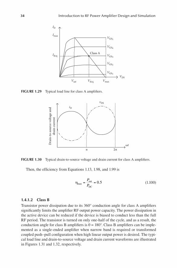
1.4.1.2 Class BTransistor power dissipation due to its 360° conduction angle for class A amplifiers significantly limits the amplifier RF output power capacity. The power dissipation in the active device can be reduced if the device is biased to conduct less than the full RF period. The transistor is turned on only one-half of the cycle, and as a result, the conduction angle for class B amplifiers is θ = 180°. Class B amplifiers can be imple-mented as a single-ended amplifier when narrow band is required or transformed coupled push–pull configuration when high linear output power is desired. The typi-cal load line and drain-to-source voltage and drain current waveforms are illustrated in Figures 1.31 and 1.32, respectively.
VDS
ID
Vsat
Class A
Imax
VmaxVdcq
Idcq
VGS1
VGS2
VGS3
VGS4
VGS5
FIGURE 1.29 Typical load line for class A amplifiers.
vDSiD
π 2πωtDra
in-to
-sou
rce v
olta
ge an
ddr
ain
curr
ent
FIGURE 1.30 Typical drain-to-source voltage and drain current for class A amplifiers.
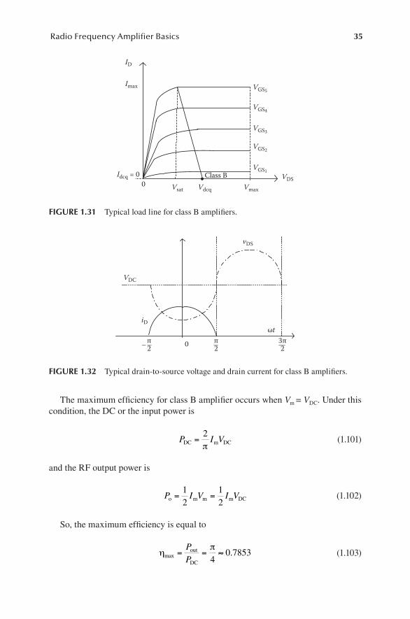
35Radio Frequency Amplifier Basics
The maximum efficiency for class B amplifier occurs when Vm = VDC. Under this condition, the DC or the input power is
P I VDC m DC=2π
(1.101)
and the RF output power is
P I V I Vo m m m DC= =12
12
(1.102)
So, the maximum efficiency is equal to
ηπ
max .= = ≈PPout
DC 40 7853 (1.103)
VDS
ID
Idcq = 0Vsat Vdcq Vmax
Class B
Imax VGS5
VGS4
VGS3
VGS2
VGS1
0
FIGURE 1.31 Typical load line for class B amplifiers.
vDS
iD
2π
2π
23π
ωt
VDC
0–
FIGURE 1.32 Typical drain-to-source voltage and drain current for class B amplifiers.
36 Introduction to RF Power Amplifier Design and Simulation
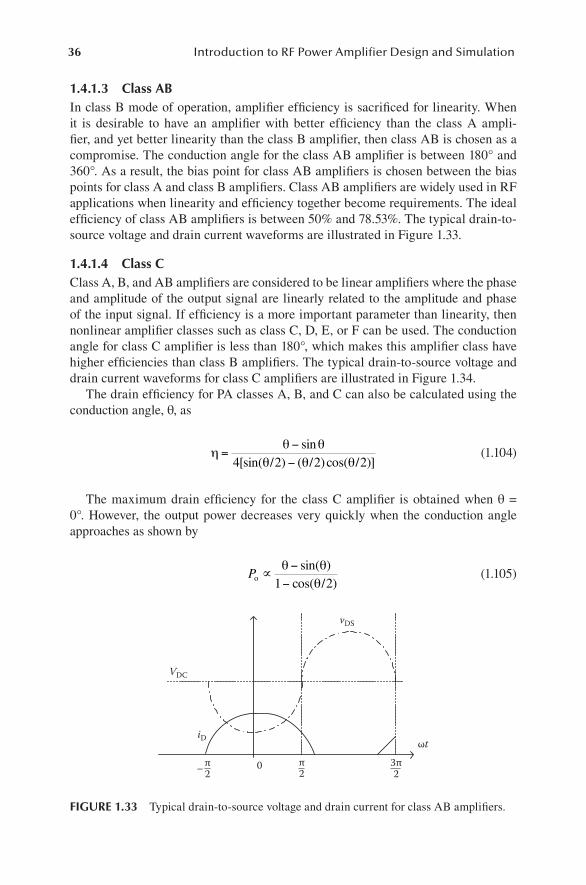
1.4.1.3 Class ABIn class B mode of operation, amplifier efficiency is sacrificed for linearity. When it is desirable to have an amplifier with better efficiency than the class A ampli-fier, and yet better linearity than the class B amplifier, then class AB is chosen as a compromise. The conduction angle for the class AB amplifier is between 180° and 360°. As a result, the bias point for class AB amplifiers is chosen between the bias points for class A and class B amplifiers. Class AB amplifiers are widely used in RF applications when linearity and efficiency together become requirements. The ideal efficiency of class AB amplifiers is between 50% and 78.53%. The typical drain-to-source voltage and drain current waveforms are illustrated in Figure 1.33.
1.4.1.4 Class CClass A, B, and AB amplifiers are considered to be linear amplifiers where the phase and amplitude of the output signal are linearly related to the amplitude and phase of the input signal. If efficiency is a more important parameter than linearity, then nonlinear amplifier classes such as class C, D, E, or F can be used. The conduction angle for class C amplifier is less than 180°, which makes this amplifier class have higher efficiencies than class B amplifiers. The typical drain-to-source voltage and drain current waveforms for class C amplifiers are illustrated in Figure 1.34.
The drain efficiency for PA classes A, B, and C can also be calculated using the conduction angle, θ, as
ηθ θ
θ θ θ=
−−
sin[sin( ) ( )cos( )]4 2 2 2/ / /
(1.104)
The maximum drain efficiency for the class C amplifier is obtained when θ = 0°. How ever, the output power decreases very quickly when the conduction angle approaches as shown by
Po /∝
θ θθ
−−
sin( )cos( )1 2
(1.105)
vDS
iD
2
VDC
02
3ππωt
2π–
FIGURE 1.33 Typical drain-to-source voltage and drain current for class AB amplifiers.
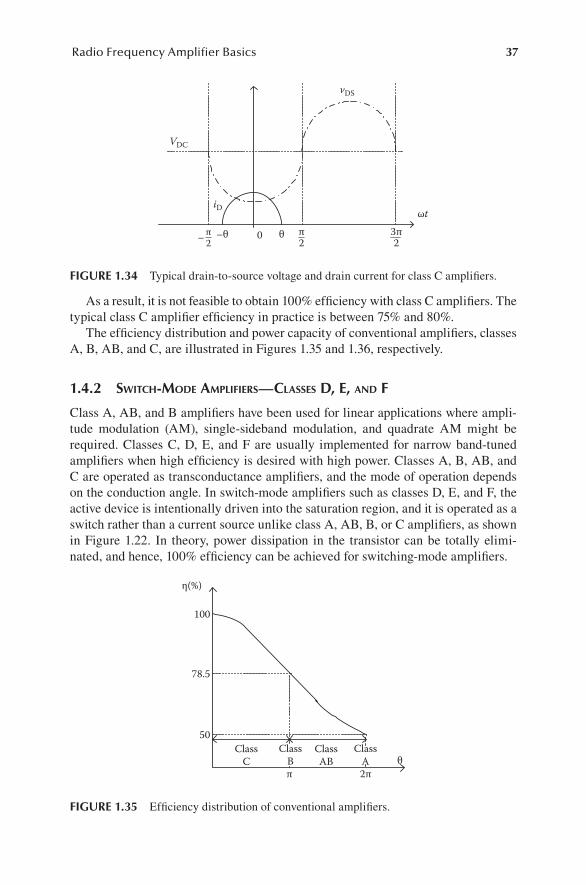
37Radio Frequency Amplifier Basics
As a result, it is not feasible to obtain 100% efficiency with class C amplifiers. The typical class C amplifier efficiency in practice is between 75% and 80%.
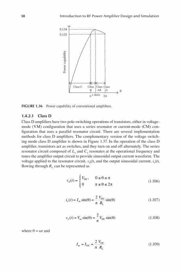
The efficiency distribution and power capacity of conventional amplifiers, classes A, B, AB, and C, are illustrated in Figures 1.35 and 1.36, respectively.
1.4.2 switcH-modE amPlifiErs—classEs d, E, and f
Class A, AB, and B amplifiers have been used for linear applications where ampli-tude modulation (AM), single-sideband modulation, and quadrate AM might be required. Classes C, D, E, and F are usually implemented for narrow band-tuned amplifiers when high efficiency is desired with high power. Classes A, B, AB, and C are operated as transconductance amplifiers, and the mode of operation depends on the conduction angle. In switch-mode amplifiers such as classes D, E, and F, the active device is intentionally driven into the saturation region, and it is operated as a switch rather than a current source unlike class A, AB, B, or C amplifiers, as shown in Figure 1.22. In theory, power dissipation in the transistor can be totally elimi-nated, and hence, 100% efficiency can be achieved for switching-mode amplifiers.
vDS
iD
VDC
0–θ θ2π– 2
3πωt
2π
FIGURE 1.34 Typical drain-to-source voltage and drain current for class C amplifiers.
100
78.5
50
η(%)
ClassC
ClassB
ClassAB
ClassA θ
π 2π
FIGURE 1.35 Efficiency distribution of conventional amplifiers.
38 Introduction to RF Power Amplifier Design and Simulation
1.4.2.1 Class DClass D amplifiers have two pole-switching operations of transistors, either in voltage- mode (VM) configuration that uses a series resonator or current-mode (CM) con-figuration that uses a parallel resonator circuit. There are several implementation methods for class D amplifiers. The complementary version of the voltage switch-ing mode class D amplifier is shown in Figure 1.37. In the operation of the class D amplifier, transistors act as switches, and they turn on and off alternately. The series resonator circuit composed of Lo and Co resonates at the operational frequency and tunes the amplifier output circuit to provide sinusoidal output current waveform. The voltage applied to the resonator circuit, vd(t), and the output sinusoidal current, io(t), flowing through RL can be represented as
v tV
dDC
0( )
,=
≤ ≤
≤ ≤
0
2
θ π
π θ π (1.106)
i t IVRo mDC
L
( ) sin( ) sin( )= =θπ
θ2
(1.107)
v t V Vo m DC( ) sin( ) sin( )= =θπ
θ2
(1.108)
where θ = ωt and
I IVRm DCDC
L
= =2π
(1.109)
Pow
er ca
pabi
lity
0.1250.134
Class Cθ
π 2π
ClassAB
1.362π
ClassB
ClassA
FIGURE 1.36 Power capability of conventional amplifiers.
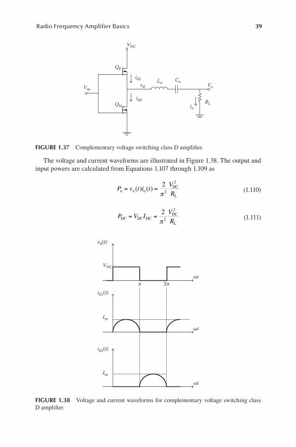
39Radio Frequency Amplifier Basics
The voltage and current waveforms are illustrated in Figure 1.38. The output and input powers are calculated from Equations 1.107 through 1.109 as
P v t i tVRo o oDC
L
= =( ) ( )22
2
π (1.110)
P V IVRDC DC DCDC
L
= =22
2
π (1.111)
Vin
RL
Vo
VDC
id1
id2
vd
io
QP
QN
Lo Co
FIGURE 1.37 Complementary voltage switching class D amplifier.
vd(t)
id1(t)
VDC
Im
Im
id2(t)
2πωt
ωt
ωt
π
FIGURE 1.38 Voltage and current waveforms for complementary voltage switching class D amplifier.
40 Introduction to RF Power Amplifier Design and Simulation
As a result, in theory, for class D amplifiers, Po = PDC, so the efficiency is equal to 100%, as shown in the following equation:
η(%) %= × =PP
o
DC
100 100 (1.112)
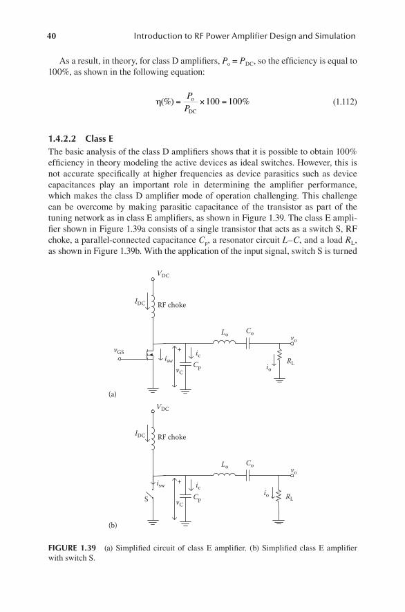
1.4.2.2 Class EThe basic analysis of the class D amplifiers shows that it is possible to obtain 100% efficiency in theory modeling the active devices as ideal switches. However, this is not accurate specifically at higher frequencies as device parasitics such as device capacitances play an important role in determining the amplifier performance, which makes the class D amplifier mode of operation challenging. This challenge can be overcome by making parasitic capacitance of the transistor as part of the tuning network as in class E amplifiers, as shown in Figure 1.39. The class E ampli-fier shown in Figure 1.39a consists of a single transistor that acts as a switch S, RF choke, a parallel-connected capacitance Cp, a resonator circuit L–C, and a load RL, as shown in Figure 1.39b. With the application of the input signal, switch S is turned
VDC
(a)
(b)
RF chokeIDC
CpRL
vo
vCio
Lo Co
iswic
+vGS
VDC
RF chokeIDC
Cp RL
vo
vC
io
Lo Co
isw ic+
S
FIGURE 1.39 (a) Simplified circuit of class E amplifier. (b) Simplified class E amplifier with switch S.
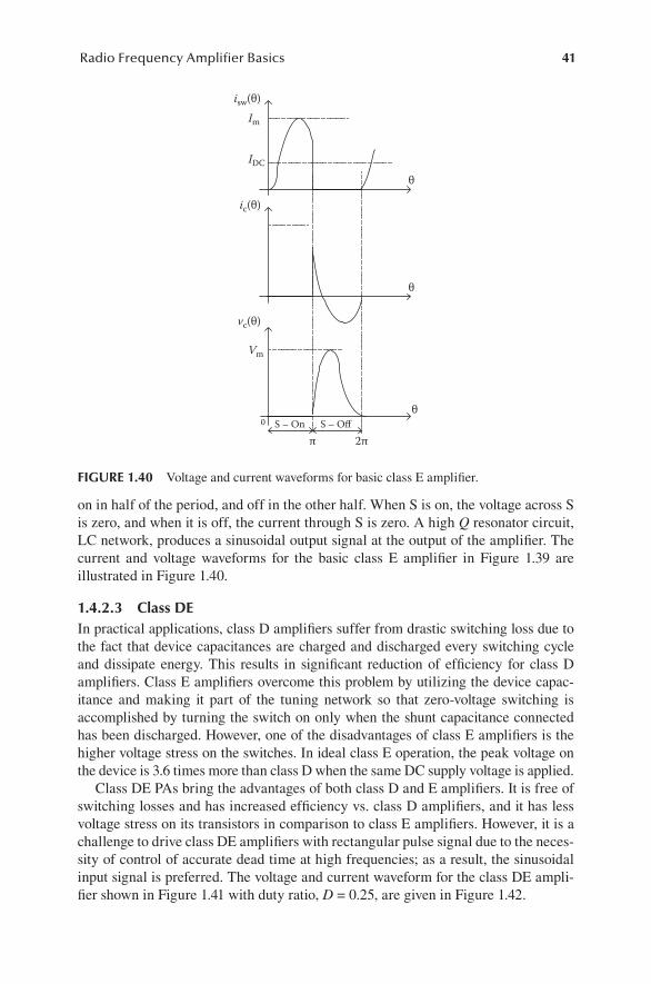
41Radio Frequency Amplifier Basics
on in half of the period, and off in the other half. When S is on, the voltage across S is zero, and when it is off, the current through S is zero. A high Q resonator circuit, LC network, produces a sinusoidal output signal at the output of the amplifier. The current and voltage waveforms for the basic class E amplifier in Figure 1.39 are illustrated in Figure 1.40.
1.4.2.3 Class DEIn practical applications, class D amplifiers suffer from drastic switching loss due to the fact that device capacitances are charged and discharged every switching cycle and dissipate energy. This results in significant reduction of efficiency for class D amplifiers. Class E amplifiers overcome this problem by utilizing the device capac-itance and making it part of the tuning network so that zero-voltage switching is accomplished by turning the switch on only when the shunt capacitance connected has been discharged. However, one of the disadvantages of class E amplifiers is the higher voltage stress on the switches. In ideal class E operation, the peak voltage on the device is 3.6 times more than class D when the same DC supply voltage is applied.
Class DE PAs bring the advantages of both class D and E amplifiers. It is free of switching losses and has increased efficiency vs. class D amplifiers, and it has less voltage stress on its transistors in comparison to class E amplifiers. However, it is a challenge to drive class DE amplifiers with rectangular pulse signal due to the neces-sity of control of accurate dead time at high frequencies; as a result, the sinusoidal input signal is preferred. The voltage and current waveform for the class DE ampli-fier shown in Figure 1.41 with duty ratio, D = 0.25, are given in Figure 1.42.
isw(θ)
θ
θ
θ
π 2π
ic(θ)
vc(θ)
0 S – On S – Off
Im
Vm
IDC
FIGURE 1.40 Voltage and current waveforms for basic class E amplifier.
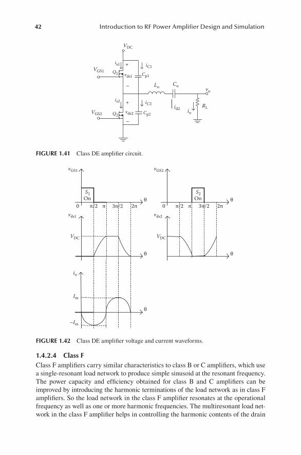
42 Introduction to RF Power Amplifier Design and Simulation
1.4.2.4 Class FClass F amplifiers carry similar characteristics to class B or C amplifiers, which use a single-resonant load network to produce simple sinusoid at the resonant frequency. The power capacity and efficiency obtained for class B and C amplifiers can be improved by introducing the harmonic terminations of the load network as in class F amplifiers. So the load network in the class F amplifier resonates at the operational frequency as well as one or more harmonic frequencies. The multiresonant load net-work in the class F amplifier helps in controlling the harmonic contents of the drain
VDC
Cp1
Cp2
iC1is1
is2
vds1
vds2
Q1
Q2
iC2+
–
+
–
VGS1
VGS2
CoLo vo
ioid2 RL
FIGURE 1.41 Class DE amplifier circuit.
0θ
π/2 3π/2π 2π π/2 3π/2π 2πθ
θ
θ
θ
vGS1 vGS2
vds1
VDC
Im
–Im
io
VDC
vds2
S1On
S2On
0
FIGURE 1.42 Class DE amplifier voltage and current waveforms.
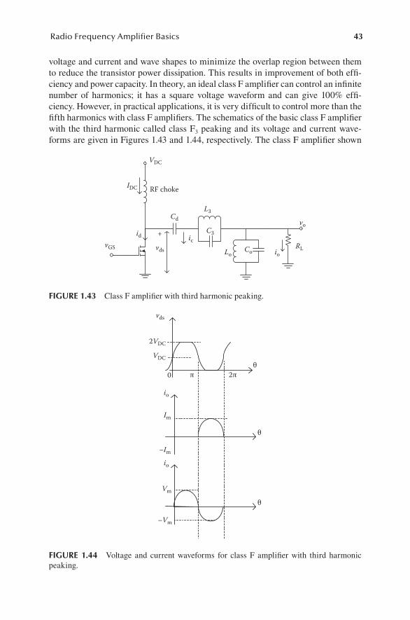
43Radio Frequency Amplifier Basics
voltage and current and wave shapes to minimize the overlap region between them to reduce the transistor power dissipation. This results in improvement of both effi-ciency and power capacity. In theory, an ideal class F amplifier can control an infinite number of harmonics; it has a square voltage waveform and can give 100% effi-ciency. However, in practical applications, it is very difficult to control more than the fifth harmonics with class F amplifiers. The schematics of the basic class F amplifier with the third harmonic called class F3 peaking and its voltage and current wave-forms are given in Figures 1.43 and 1.44, respectively. The class F amplifier shown
VDC
RF chokeIDC
Cd
RL
vo
vds io
id ic+
vGS
L3
C3
LoCo
FIGURE 1.43 Class F amplifier with third harmonic peaking.
vds
io
io
Im
Vm
–Im
–Vm
2VDC
VDC
0θ
π 2π
θ
θ
FIGURE 1.44 Voltage and current waveforms for class F amplifier with third harmonic peaking.
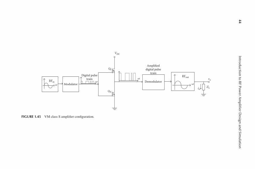
44In
trod
uctio
n to
RF Po
wer A
mp
lifier D
esign an
d Sim
ulatio
n
VDC
QP
QN
Modulatorωt
Digital pulsetrain
Demodulator
Amplifieddigital pulse
train
vo
ioZL
RFoutRFin ωt
ωt
ωt
FIGURE 1.45 VM class S amplifier configuration.
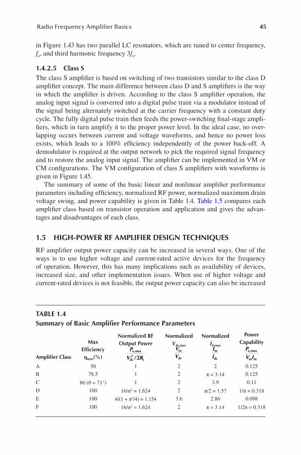
45Radio Frequency Amplifier Basics
in Figure 1.43 has two parallel LC resonators, which are tuned to center frequency, fo, and third harmonic frequency 3fo.
1.4.2.5 Class SThe class S amplifier is based on switching of two transistors similar to the class D amplifier concept. The main difference between class D and S amplifiers is the way in which the amplifier is driven. According to the class S amplifier operation, the analog input signal is converted into a digital pulse train via a modulator instead of the signal being alternately switched at the carrier frequency with a constant duty cycle. The fully digital pulse train then feeds the power-switching final-stage ampli-fiers, which in turn amplify it to the proper power level. In the ideal case, no over-lapping occurs between current and voltage waveforms, and hence no power loss exists, which leads to a 100% efficiency independently of the power back-off. A demodulator is required at the output network to pick the required signal frequency and to restore the analog input signal. The amplifier can be implemented in VM or CM configurations. The VM configuration of class S amplifiers with waveforms is given in Figure 1.45.
The summary of some of the basic linear and nonlinear amplifier performance parameters including efficiency, normalized RF power, normalized maximum drain voltage swing, and power capability is given in Table 1.4. Table 1.5 compares each amplifier class based on transistor operation and application and gives the advan-tages and disadvantages of each class.
1.5 HIGH-POWER RF AMPLIFIER DESIGN TECHNIQUES
RF amplifier output power capacity can be increased in several ways. One of the ways is to use higher voltage and current-rated active devices for the frequency of operation. However, this has many implications such as availability of devices, increased size, and other implementation issues. When use of higher voltage and current-rated devices is not feasible, the output power capacity can also be increased
TABLE 1.4Summary of Basic Amplifier Performance Parameters
Amplifier Class
Max Efficiencyηmax(%)
Normalized RF Output Power
P
V Ro
dc L/,max
2 2
Normalized Vds,maxVV
m
dc
Normalized Id,maxIIm
dc
Power CapabilityPV Io
m m
,max
A 50 1 2 2 0.125
B 78.5 1 2 π = 3.14 0.125
C 86 (θ = 71°) 1 2 3.9 0.11
D 100 16/π2 = 1.624 2 π/2 = 1.57 1/π = 0.318
E 100 4/(1 + π2/4) = 1.154 3.6 2.86 0.098
F 100 16/π2 = 1.624 2 π = 3.14 1/2π = 0.318
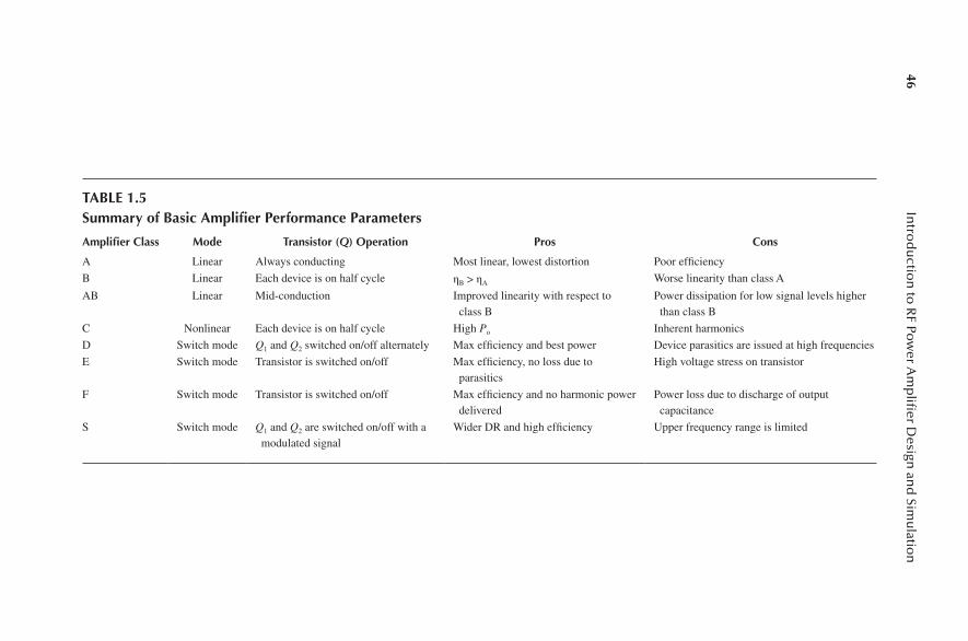
46In
trod
uctio
n to
RF Po
wer A
mp
lifier D
esign an
d Sim
ulatio
n
TABLE 1.5Summary of Basic Amplifier Performance Parameters
Amplifier Class Mode Transistor (Q) Operation Pros Cons
A Linear Always conducting Most linear, lowest distortion Poor efficiency
B Linear Each device is on half cycle ηB > ηA Worse linearity than class A
AB Linear Mid-conduction Improved linearity with respect to class B
Power dissipation for low signal levels higher than class B
C Nonlinear Each device is on half cycle High Po Inherent harmonics
D Switch mode Q1 and Q2 switched on/off alternately Max efficiency and best power Device parasitics are issued at high frequencies
E Switch mode Transistor is switched on/off Max efficiency, no loss due to parasitics
High voltage stress on transistor
F Switch mode Transistor is switched on/off Max efficiency and no harmonic power delivered
Power loss due to discharge of output capacitance
S Switch mode Q1 and Q2 are switched on/off with a modulated signal
Wider DR and high efficiency Upper frequency range is limited

47Radio Frequency Amplifier Basics
by using push–pull configuration and/or parallel transistor configuration. The fol-lowing discussion describes how these two techniques can be implemented.
1.5.1 PusH–Pull amPlifiEr confiGuration
Practical RF PA design uses push–pull configuration widely to meet with the demand of high output power. The input drive signal for push–pull amplifiers is outphased by 180° using transformers such as input balun. Output balun is used at the output to combine the outphased amplifier output signal and double the RF power. The RF input voltage signal at operational frequency, ignoring the phases and assuming ideal conditions for simplicity, can be expressed as
vs(t) = 4Vm sin(ωt) (1.113)
Assuming the matched impedance case, the signal at the input of the balun is then
v tv t
V tins
m( )( )
sin( )= =2
2 ω (1.114)
The signal at the output of the balun will be equally split and phased by 180°. These signals at the input of the amplifiers can be represented as
v1(t) = Vm sin(ωt) (1.115)
v2(t) = Vm sin(ωt + θ) = −Vm sin(ωt) (1.116)
where θ = 180°.The signals v1(t) and v2(t) will be amplified by the amplifiers by their corresponding
gains, A1 and A2, respectively. The signals at the output of the amplifiers are then equal to
v1(t) = A1Vm sin(ωt) (1.117)
v2(t) = −A2Vm sin(ωt) (1.118)
The amplifier output signals are then combined via the output balun. The final load signal is
vL(t) = v1(t) − v2(t) = (A1 + A2)Vm sin(ωt) (1.119)
The illustration of the push–pull amplifier with waveforms is given in Figure 1.46.
1.5.2 ParallEl transistor confiGuration
RF power output in the amplifier system can be increased by also paralleling the tran-sistors. When transistors are paralleled, the current is increased proportional to the number of transistors used under ideal conditions. This can be illustrated in Figure 1.47.
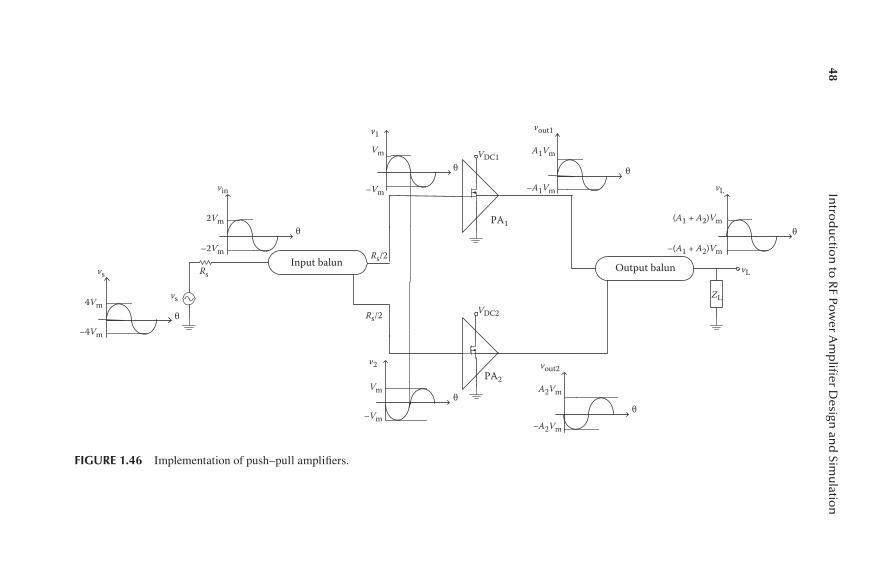
48In
trod
uctio
n to
RF Po
wer A
mp
lifier D
esign an
d Sim
ulatio
n
Input balun
PA1
Output balunRs
vout1v1
Vm
–Vm
v2
Vm
–Vm
vL
vL
ZL
A1Vm
(A1 + A2)Vm
–(A1 + A2)Vm
–A1Vm
θ
vin
2Vm
4Vm
–4Vm
vs
vs
–2Vm
θ
θ
θ
θ
θ
θ
PA2vout2
VDC2
Rs/2
Rs/2
VDC1
A2Vm
–A2Vm
FIGURE 1.46 Implementation of push–pull amplifiers.
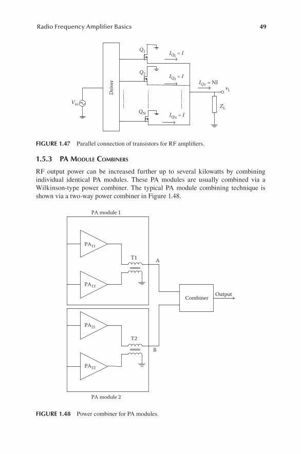
49Radio Frequency Amplifier Basics
1.5.3 Pa modulE combinErs
RF output power can be increased further up to several kilowatts by combining individual identical PA modules. These PA modules are usually combined via a Wilkinson-type power combiner. The typical PA module combining technique is shown via a two-way power combiner in Figure 1.48.
Q1
Q2
QN
Vin
vLIQT = NI
ZL
IQ1 = I
IQ2 = I
IQN = ID
river
FIGURE 1.47 Parallel connection of transistors for RF amplifiers.
Combiner
A
B
Output
PA module 2
PA module 1
T1
T2
PA11
PA12
PA21
PA22
FIGURE 1.48 Power combiner for PA modules.
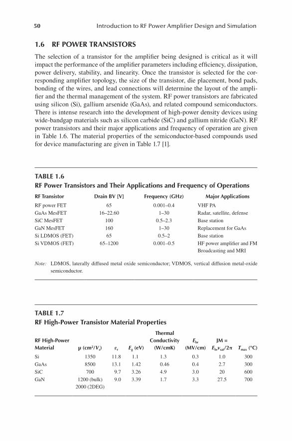
50 Introduction to RF Power Amplifier Design and Simulation
1.6 RF POWER TRANSISTORS
The selection of a transistor for the amplifier being designed is critical as it will impact the performance of the amplifier parameters including efficiency, dissipation, power delivery, stability, and linearity. Once the transistor is selected for the cor-responding amplifier topology, the size of the transistor, die placement, bond pads, bonding of the wires, and lead connections will determine the layout of the ampli-fier and the thermal management of the system. RF power transistors are fabricated using silicon (Si), gallium arsenide (GaAs), and related compound semiconductors. There is intense research into the development of high-power density devices using wide-bandgap materials such as silicon carbide (SiC) and gallium nitride (GaN). RF power transistors and their major applications and frequency of operation are given in Table 1.6. The material properties of the semiconductor-based compounds used for device manufacturing are given in Table 1.7 [1].
TABLE 1.6RF Power Transistors and Their Applications and Frequency of Operations
RF Transistor Drain BV [V] Frequency (GHz) Major Applications
RF power FET 65 0.001–0.4 VHF PA
GaAs MesFET 16–22.60 1–30 Radar, satellite, defense
SiC MesFET 100 0.5–2.3 Base station
GaN MesFET 160 1–30 Replacement for GaAs
Si LDMOS (FET) 65 0.5–2 Base station
Si VDMOS (FET) 65–1200 0.001–0.5 HF power amplifier and FMBroadcasting and MRI
Note: LDMOS, laterally diffused metal oxide semiconductor; VDMOS, vertical diffusion metal-oxide semiconductor.
TABLE 1.7RF High-Power Transistor Material Properties
RF High-Power Material μ (cm2/Vs) εr Eg (eV)
Thermal Conductivity
(W/cmK)Ebr
(MV/ cm)JM =
Ebrvsat/2π Tmax (°C)
Si 1350 11.8 1.1 1.3 0.3 1.0 300
GaAs 8500 13.1 1.42 0.46 0.4 2.7 300
SiC 700 9.7 3.26 4.9 3.0 20 600
GaN 1200 (bulk)2000 (2DEG)
9.0 3.39 1.7 3.3 27.5 700
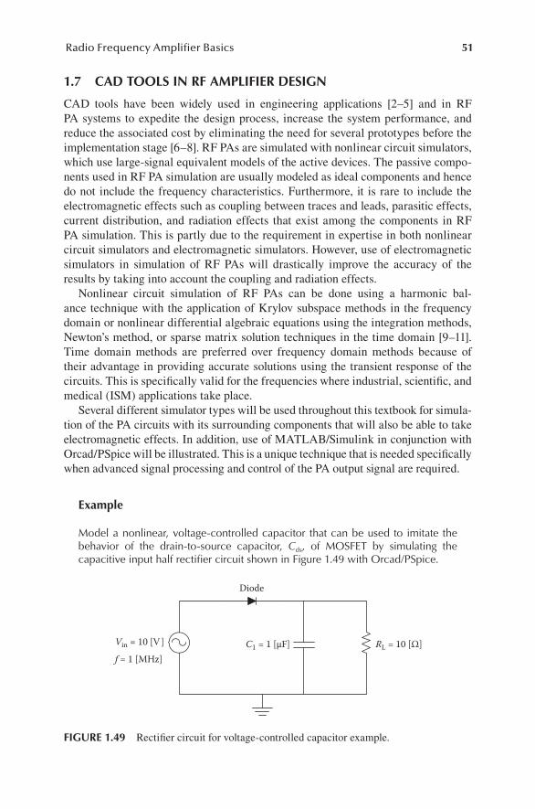
51Radio Frequency Amplifier Basics
1.7 CAD TOOLS IN RF AMPLIFIER DESIGN
CAD tools have been widely used in engineering applications [2–5] and in RF PA systems to expedite the design process, increase the system performance, and reduce the associated cost by eliminating the need for several prototypes before the implementation stage [6–8]. RF PAs are simulated with nonlinear circuit simulators, which use large-signal equivalent models of the active devices. The passive compo-nents used in RF PA simulation are usually modeled as ideal components and hence do not include the frequency characteristics. Furthermore, it is rare to include the electromagnetic effects such as coupling between traces and leads, parasitic effects, current distribution, and radiation effects that exist among the components in RF PA simulation. This is partly due to the requirement in expertise in both nonlinear circuit simulators and electromagnetic simulators. However, use of electromagnetic simulators in simulation of RF PAs will drastically improve the accuracy of the results by taking into account the coupling and radiation effects.
Nonlinear circuit simulation of RF PAs can be done using a harmonic bal-ance technique with the application of Krylov subspace methods in the frequency domain or nonlinear differential algebraic equations using the integration methods, Newton’s method, or sparse matrix solution techniques in the time domain [9–11]. Time domain methods are preferred over frequency domain methods because of their advantage in providing accurate solutions using the transient response of the circuits. This is specifically valid for the frequencies where industrial, scientific, and medical (ISM) applications take place.
Several different simulator types will be used throughout this textbook for simula-tion of the PA circuits with its surrounding components that will also be able to take electromagnetic effects. In addition, use of MATLAB/Simulink in conjunction with Orcad/PSpice will be illustrated. This is a unique technique that is needed specifically when advanced signal processing and control of the PA output signal are required.
Example
Model a nonlinear, voltage-controlled capacitor that can be used to imitate the behavior of the drain-to-source capacitor, Cds, of MOSFET by simulating the capacitive input half rectifier circuit shown in Figure 1.49 with Orcad/PSpice.
C1 = 1 [µF] RL = 10 [Ω]Vin = 10 [V ]
f = 1 [MHz]
Diode
FIGURE 1.49 Rectifier circuit for voltage-controlled capacitor example.
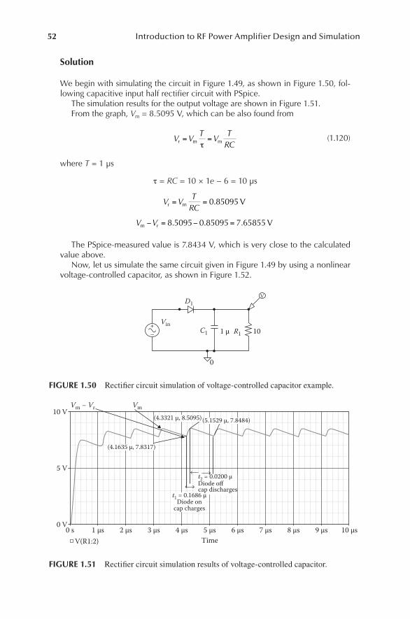
52 Introduction to RF Power Amplifier Design and Simulation
Solution
We begin with simulating the circuit in Figure 1.49, as shown in Figure 1.50, fol-lowing capacitive input half rectifier circuit with PSpice.
The simulation results for the output voltage are shown in Figure 1.51.From the graph, Vm = 8.5095 V, which can be also found from
V VT
VTRCr m m= =
τ (1.120)
where T = 1 µs
τ = RC = 10 × 1e − 6 = 10 µs
V VTRC
V V
r m
m r
V
V
= =
− = − =
0 85095
8 5095 0 85095 7 65855
.
. . .
The PSpice-measured value is 7.8434 V, which is very close to the calculated value above.
Now, let us simulate the same circuit given in Figure 1.49 by using a nonlinear voltage-controlled capacitor, as shown in Figure 1.52.
D1
C1 1 μ R1 10
0
Vin+–
V
FIGURE 1.50 Rectifier circuit simulation of voltage-controlled capacitor example.
(4.1635 µ, 7.8317)
Time0 s
0 V
5 V
10 VVm − Vr Vm
1 µs 2 µs 3 µs 4 µs 5 µs 6 µs 7 µs 8 µs 9 µs 10 µsV(R1:2)
t1 = 0.1686 µDiode on
cap charges
(4.3321 µ, 8.5095)(5.1529 µ, 7.8484)
t2 = 0.0200 µDiode offcap discharges
FIGURE 1.51 Rectifier circuit simulation results of voltage-controlled capacitor.
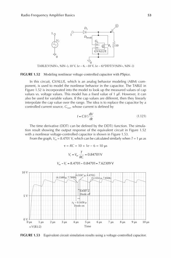
53Radio Frequency Amplifier Basics
In this circuit, GVALUE, which is an analog behavior modeling (ABM) com-ponent, is used to model the nonlinear behavior in the capacitor. The TABLE in Figure 1.52 is incorporated into the model to look up the measured values of cap values vs. voltage values. This model has a fixed value of 1 μF. However, it can also be used for variable values. If the cap values are different, then they linearly interpolate the cap value over the range. The idea is to replace the capacitor by a controlled current source, Gout, whose current is defined by
I C VVt
= ( )dd
(1.121)
The time derivative (DDT) can be defined by the DDT() function. The simula-tion result showing the output response of the equivalent circuit in Figure 1.52 with a nonlinear voltage-controlled capacitor is shown in Figure 1.53.
From the graph, Vm = 8.4701 V, which can be calculated similarly when T = 1 μs as
τ = RC = 10 × 1e − 6 = 10 μs
V VT
V V
r m
m r
V
V
= =
− = − =
RC0 84701
8 4701 0 84701 7 62309
.
. . .
1 1
+–
D1
IN+IN–
G1R1
GVALUE
10
V
DbreakV7
0
TABLE(V(%IN+, %IN–), 10 V, 1e – 6, –10 V, 1e – 6)*DDT(V(%IN+, %IN–))0
FIGURE 1.52 Modeling nonlinear voltage-controlled capacitor with PSpice.
Time0 µs 1 µs 2 µs 3 µs 4 µs 5 µs 6 µs 7 µs 8 µs 9 µs 10 µs
V(R1:2)
0 V
5 V
10 V
0.8307 Diode off
t1 = 0.1658 µDiode on
(5.1554 µ, 7.8506)(4.3247 µ, 8.4701)
(4.1589 µ, 7.7899)
µ
FIGURE 1.53 Equivalent circuit simulation results using a voltage-controlled capacitor.
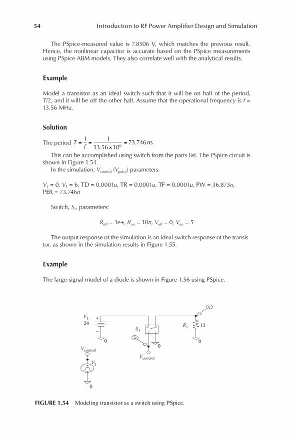
54 Introduction to RF Power Amplifier Design and Simulation
The PSpice-measured value is 7.8506 V, which matches the previous result. Hence, the nonlinear capacitor is accurate based on the PSpice measurements using PSpice ABM models. They also correlate well with the analytical results.
Example
Model a transistor as an ideal switch such that it will be on half of the period, T/2, and it will be off the other half. Assume that the operational frequency is f = 13.56 MHz.
Solution
The period Tf
= =×
=1 1
13 56 1073 7466.
. ns
This can be accomplished using switch from the parts list. The PSpice circuit is shown in Figure 1.54.
In the simulation, Vcontrol (Vpulse) parameters:
V1 = 0, V2 = 6, TD = 0.0001u, TR = 0.0001u, TF = 0.0001u, PW = 36.873n, PER = 73.746n
Switch, S1, parameters:
Roff = 1e+, Ron = 10n, Voff = 0, Von = 5
The output response of the simulation is an ideal switch response of the transis-tor, as shown in the simulation results in Figure 1.55.
Example
The large-signal model of a diode is shown in Figure 1.56 using PSpice.
+–
Vcontrol
0
S1
V2
R1 12
V
00
++ –
–
Vcontrol
V
24+
–
0
V1
FIGURE 1.54 Modeling transistor as a switch using PSpice.
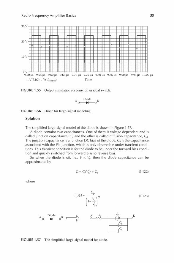
55Radio Frequency Amplifier Basics
Solution
The simplified large-signal model of the diode is shown in Figure 1.57.A diode contains two capacitances. One of them is voltage dependent and is
called junction capacitance, Cj, and the other is called diffusion capacitance, Cd. The junction capacitance is a function DC bias of the diode. Cd is the capacitance associated with the PN junction, which is only observable under transient condi-tions. This transient condition is for the diode to be under the forward bias condi-tion and quickly switched from forward bias to reverse bias.
So when the diode is off, i.e., V < Vd, then the diode capacitance can be approximated by
C = Cj(VR) + Cd (1.122)
where
C VC
VV
j Rjo
d
j
M( ) =
−
1
(1.123)
Time9.50 µs 9.55 µs 9.60 µs 9.65 µs 9.70 µs 9.75 µs 9.80 µs 9.85 µs 9.90 µs 9.95 µs 10.00 µs
V(R1:2) V(Vcontrol)
0 V
10 V
20 V
30 V
FIGURE 1.55 Output simulation response of an ideal switch.
DiodeA K
FIGURE 1.56 Diode for large-signal modeling.
DiodeA KRs
ID
Cj
Cd
A K
FIGURE 1.57 The simplified large-signal model for diode.
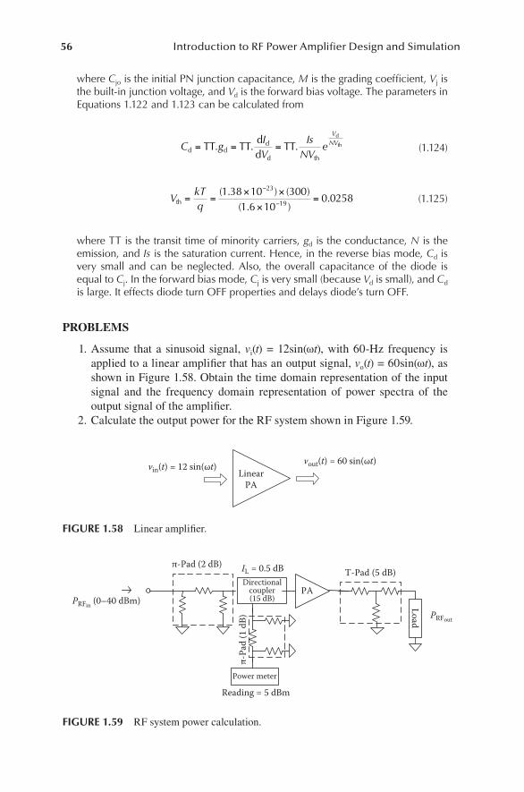
56 Introduction to RF Power Amplifier Design and Simulation
where Cjo is the initial PN junction capacitance, M is the grading coefficient, Vj is the built-in junction voltage, and Vd is the forward bias voltage. The parameters in Equations 1.122 and 1.123 can be calculated from
C gI Is
NV
VNV
d dd
d th
TT TTdd
TTd
th= = =. . .V
e (1.124)
VkTqth = =
× ×
×=
−
−
( . ) ( )( . )
.1 38 10 300
1 6 100 0258
23
19 (1.125)
where TT is the transit time of minority carriers, gd is the conductance, N is the emission, and Is is the saturation current. Hence, in the reverse bias mode, Cd is very small and can be neglected. Also, the overall capacitance of the diode is equal to Cj. In the forward bias mode, Cj is very small (because Vd is small), and Cd is large. It effects diode turn OFF properties and delays diode’s turn OFF.
PROBLEMS
1. Assume that a sinusoid signal, vi(t) = 12sin(ωt), with 60-Hz frequency is applied to a linear amplifier that has an output signal, vo(t) = 60sin(ωt), as shown in Figure 1.58. Obtain the time domain representation of the input signal and the frequency domain representation of power spectra of the output signal of the amplifier.
2. Calculate the output power for the RF system shown in Figure 1.59.
LinearPA
vout(t) = 60 sin(ωt)vin(t) = 12 sin(ωt)
FIGURE 1.58 Linear amplifier.
Directionalcoupler(15 dB)
PA
Power meter
Reading = 5 dBm
π-Pad (2 dB) IL = 0.5 dB T-Pad (5 dB)
π-Pa
d (1
dB) PRFout
PRFin (0–40 dBm) Load
FIGURE 1.59 RF system power calculation.
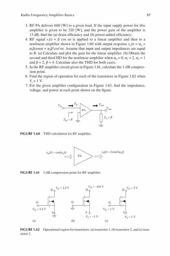
57Radio Frequency Amplifier Basics
3. RF PA delivers 600 [W] to a given load. If the input supply power for this amplifier is given to be 320 [W], and the power gain of the amplifier is 13 dB, find the (a) drain efficiency and (b) power-added efficiency.
4. RF signal vi(t) = β cos ωt is applied to a linear amplifier and then to a nonlinear amplifier shown in Figure 1.60 with output response vo(t) = α0 + α1βcosωt + α2β2cos2ωt. Assume that input and output impedances are equal to R. (a) Calculate and plot the gain for the linear amplifier. (b) Obtain the second and third HD for the nonlinear amplifier when α0 = 0, α1 = 2, α2 = 1 and β = 2, β = 4. Calculate also the THD for both cases.
5. In the RF amplifier circuit given in Figure 1.61, calculate the 1-dB compres-sion point.
6. Find the region of operation for each of the transistors in Figure 1.62 when Vt = 1 V.
7. For the given amplifier configuration in Figure 1.63, find the impedance, voltage, and power at each point shown on the figure.
Vin
PA
Pin
ZL = RZin = R
PoutVout
FIGURE 1.60 THD calculation for RF amplifier.
PAv3(t) = 5cos(3ωot)vin(t) = cos(ωot)
FIGURE 1.61 1-dB compression point for RF amplifier.
D
G
S
VD = 2.2 V VD = –0.6 V VD = 3 V
VS = 1 VVS = –1 V
VG = 2.2 V VG = 1 V
D
G
S
D
G
S
(a) (b) (c)
FIGURE 1.62 Operational region for transistors: (a) transistor 1, (b) transistor 2, and (c) tran-sistor 3.
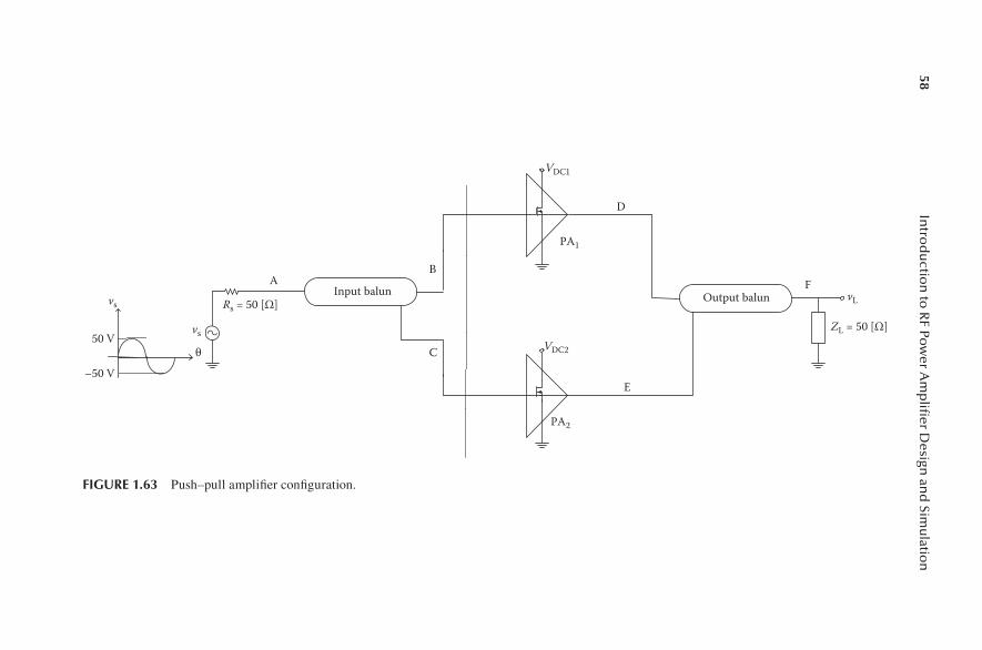
58In
trod
uctio
n to
RF Po
wer A
mp
lifier D
esign an
d Sim
ulatio
n
Input balun
PA2
PA1
Output balun vL
ZL = 50 [Ω]
Rs = 50 [Ω]
VDC1
VDC2
vs
vs
A
50 Vθ
–50 V
B
C
D
E
F
FIGURE 1.63 Push–pull amplifier configuration.
59Radio Frequency Amplifier Basics
REFERENCES
1. U.K. Mishra, L. Shen, T.E. Kazior, and Y.-F. Wu. 2008. GaN-based RF power devices and amplifiers. Proceedings of the IEEE, Vol. 96, No. 2, pp. 287–305, February.
2. S. El Alimi, C. Münch, A. Azzi, P. Bégou, and S.B. Nasrallah. 2009. Large eddy simu-lation of a compressible flow in a locally heated square duct. International Review of Modeling and Simulations (IREMOS), Vol. 2, No. 1, pp. 93–97, February.
3. O. Chocron, and H. Mangel. 2011. Models and simulations for reconfigurable magnetic- coupling thrusters technology. International Review of Modeling and Simulations (IREMOS), Vol. 4, No. 1, pp. 325–334, February.
4. A. Milovanovic, B. Koprivica, and M. Bjekic. 2010. Application of the charge simu-lation method to the calculation of the characteristic parameters of printed transmis-sion lines. International Review of Electrical Engineering (IREE), Vol. 5, No. 6, Pt. A, pp. 2722–2726, December.
5. M. Heidari, R. Kianinezhad, S.Gh. Seifossadat, M. Monadi, and D. Mirabbasi. 2011. Effects of distribution network unbalance voltage types with identical unbalance factor on the induction motors simulation and experimental. International Review of Electrical Engineering (IREE), Vol. 6, No. 1, Pt. A, pp. 223–228, February.
6. P.H. Aaen, J.A. Pla, and C.A. Balanis. 2006. Modeling techniques suitable for CAD-based design of internal matching networks of high-power RF/microwave transistors. IEEE Transactions on Microwave Theory and Techniques, Vol. 54, No. 7, pp. 3052–3059, July.
7. R. Mittra, and V. Veremey. 2000. Computer-aided design of RF circuits. 2000 IEEE AP-S, Vol. 2, pp. 596–599, Salt Lake City.
8. K.C. Gupta. 1998. Emerging trends in millimeter-wave CAD. IEEE Transactions on Microwave Theory and Techniques, Vol. 46, No. 6, pp. 747–755, June.
9. R.J. Gilmore, and M.B. Steer. 1991. Nonlinear circuit analysis using the method of harmonic balance—A review of the art. Part I. Introductory concepts. International Journal of Microwave and Millimeter-Wave Computer-Aided Engineering, Vol. 1, No. 1, pp. 22–37.
10. R.J. Gilmore, and M.B. Steer. 1991. Nonlinear circuit analysis using the method of harmonic balance—A review of the art. Part II. Advanced concepts. International Journal of Microwave and Millimeter-Wave Computer-Aided Engineering, Vol. 1, No. 2, pp. 159–180.
11. K.S. Kundert. 1998. The Designer’s Guide to Spice and Spectre. Kluwer Academic Publishers, Boston.

61
2 Radio Frequency Power Transistors
2.1 INTRODUCTION
Radio frequency (RF) power transistors are the most critical components in the amplifier system since their characteristics have direct implications in amplifier response including power, stability, linearity, and the profile of the amplifier itself. The parameters of the transistor such as gain, intrinsic parameters such as capaci-tances, and extrinsic parameters such as lead inductances are determining factors of the amplifier design and performance. Transistors have small-signal and large-signal models. Small-signal models assume small variation between voltages and currents and hence do not provide an accurate design for amplifiers when large varia-tions take place between voltages and currents. It is also very challenging to obtain accurate large-signal models for active devices. Small- and large-signal models are provided by manufacturers and implemented in simulators such as advanced design system (ADS) and Orcad/PSpice environment. When the transistor model is avail-able as an equivalent circuit, the transistor then can be treated as a two-port device, as shown in Figure 2.1, and network analysis is performed to produce analytical and numerical results.
2.2 HIGH-FREQUENCY MODEL FOR MOSFETs
Metal–oxide–semiconductor field-effect transistors (MOSFETs) are the preferred active device that will be used throughout this book for illustration of the majority of the concepts and examples in RF power amplifier design. There are several dif-ferent versions of MOSFETs, which are manufactured using different processes, as illustrated in Figure 2.2.
MOSFET parameters are identified by manufacturers at different static and dynamic conditions. Hence, each MOSFET device has been manufactured with dif-ferent characteristics. A designer makes the selection of the appropriate device for the specific circuit under consideration. One of the standard ways commonly used by designers for the selection of the right MOSFET device is called figure of merit (FOM) [1]. Although there are different types of FOMs that are used, FOM in its simplest form compares the gate charge, Qg, against Rdson. The multiplication of gate charge and drain to source on resistance relates to a certain device technology as it can be related to the required Qg and Rdson to achieve the right scale for MOSFETs. The challenge is the relation between Qg and Rdson because MOSFETs have inher-ent trade-offs between the ON resistance and gate charge, i.e., the lower the Rdson is,
62 Introduction to RF Power Amplifier Design and Simulation
the higher the gate charge will be. In device design, this translates into conduction loss vs. switching loss trade-off. The new-generation MOSFETs are manufactured to have an improved FOM [2–4]. The comparison of FOM on MOSFETs manufactured with different processes can be illustrated on planar MOSFET structure and trench MOSFET structure. MOSFETs with trench structure have seven times better FOM vs. planar structure, as shown in Figure 2.3.
Two variations of trench power MOSFETs are shown in Figure 2.4. The trench technology has the advantage of higher cell density but is more difficult to manufac-ture than the planar device.
There is a best die size for MOSFET devices for a given output power. The opti-mum die size for minimal power loss, Ploss, depends on load impedance, rated power,
Two-port network
I1
V1+–
I2
V2+–
FIGURE 2.1 RF power transistor as a two-port network.
FET
MOSFET
GaA
s MO
SFET
Si M
OSF
ET
NM
OS,
PM
OS
CM
OS
HM
OS
DM
OS,
DIM
OS
VM
OS
SOS,
SO
I
MESFET
Het
eros
truc
ture
MES
FET
InP
MES
FET
GaA
s MES
FET
Si M
ESFE
T
Sing
le g
ate
Dua
l gat
eIn
terd
igita
l str
uctu
reJFET
Si JF
ET
GaA
s JFE
TD
iffus
edG
row
nH
eter
ojun
ctio
n
Sing
le c
hann
elV
-gro
ove
Mul
ticha
nnel
FIGURE 2.2 Types of MOSFETs.
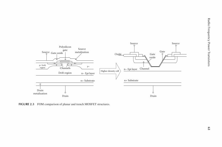
63R
adio
Frequ
ency Po
wer Tran
sistors
Source
Drain
Gate oxide
Polysilicongate Source
metalization
p+ bodyregion
n+ n+p p
Channelsp+
Drift region n– Epi layer
n+ Substrate
Drainmetalization
Channel
Gateoxide
Source
Oxide
Source
Gate
Drain
n– Epi layer
n+ Substrate
Higher density cell
FIGURE 2.3 FOM comparison of planar and trench MOSFET structures.
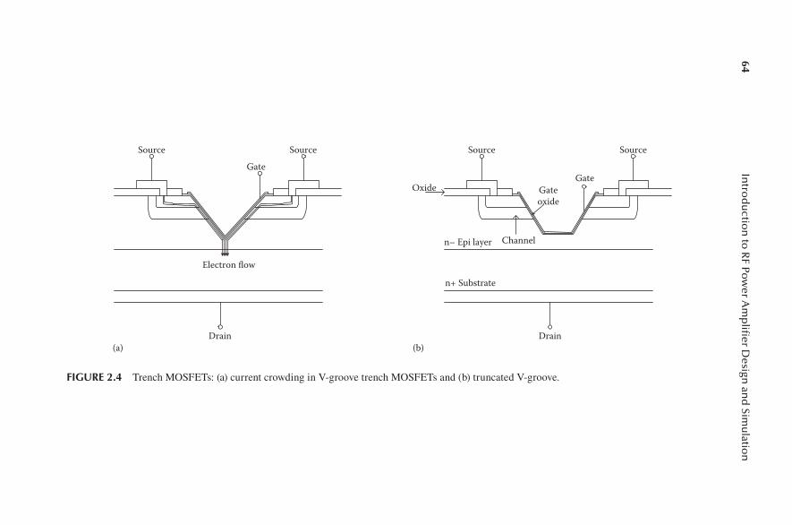
64In
trod
uctio
n to
RF Po
wer A
mp
lifier D
esign an
d Sim
ulatio
n
Channel
Gateoxide
Source
Oxide
Source
Gate
Drain
n– Epi layer
n+ Substrate
Source Source
Gate
Drain
Electron flow
(b)(a)
FIGURE 2.4 Trench MOSFETs: (a) current crowding in V-groove trench MOSFETs and (b) truncated V-groove.
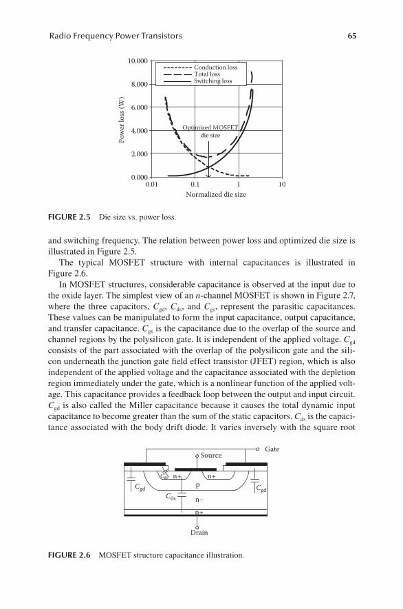
65Radio Frequency Power Transistors
and switching frequency. The relation between power loss and optimized die size is illustrated in Figure 2.5.
The typical MOSFET structure with internal capacitances is illustrated in Figure 2.6.
In MOSFET structures, considerable capacitance is observed at the input due to the oxide layer. The simplest view of an n-channel MOSFET is shown in Figure 2.7, where the three capacitors, Cgd, Cds, and Cgs, represent the parasitic capacitances. These values can be manipulated to form the input capacitance, output capacitance, and transfer capacitance. Cgs is the capacitance due to the overlap of the source and channel regions by the polysilicon gate. It is independent of the applied voltage. Cgd consists of the part associated with the overlap of the polysilicon gate and the sili-con underneath the junction gate field effect transistor (JFET) region, which is also independent of the applied voltage and the capacitance associated with the depletion region immediately under the gate, which is a nonlinear function of the applied volt-age. This capacitance provides a feedback loop between the output and input circuit. Cgd is also called the Miller capacitance because it causes the total dynamic input capacitance to become greater than the sum of the static capacitors. Cds is the capaci-tance associated with the body drift diode. It varies inversely with the square root
0.000
2.000
4.000
6.000
8.000
10.000
0.01 0.1 1 10
Conduction lossTotal lossSwitching loss
Normalized die size
Pow
er lo
ss (W
)Optimized MOSFET
die size
FIGURE 2.5 Die size vs. power loss.
n+ n+CgdCgd
Cds
Cgs
n–n+
p
GateSource
Drain
FIGURE 2.6 MOSFET structure capacitance illustration.
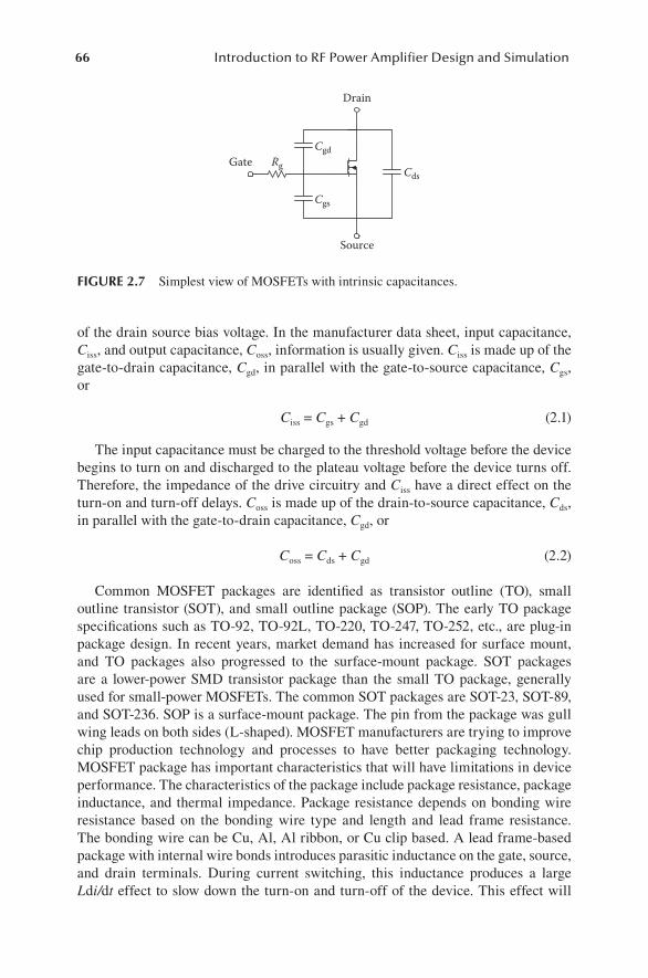
66 Introduction to RF Power Amplifier Design and Simulation
of the drain source bias voltage. In the manufacturer data sheet, input capacitance, Ciss, and output capacitance, Coss, information is usually given. Ciss is made up of the gate-to-drain capacitance, Cgd, in parallel with the gate-to-source capacitance, Cgs, or
Ciss = Cgs + Cgd (2.1)
The input capacitance must be charged to the threshold voltage before the device begins to turn on and discharged to the plateau voltage before the device turns off. Therefore, the impedance of the drive circuitry and Ciss have a direct effect on the turn-on and turn-off delays. Coss is made up of the drain-to-source capacitance, Cds, in parallel with the gate-to-drain capacitance, Cgd, or
Coss = Cds + Cgd (2.2)
Common MOSFET packages are identified as transistor outline (TO), small outline transistor (SOT), and small outline package (SOP). The early TO package specifications such as TO-92, TO-92L, TO-220, TO-247, TO-252, etc., are plug-in package design. In recent years, market demand has increased for surface mount, and TO packages also progressed to the surface-mount package. SOT packages are a lower-power SMD transistor package than the small TO package, generally used for small-power MOSFETs. The common SOT packages are SOT-23, SOT-89, and SOT-236. SOP is a surface-mount package. The pin from the package was gull wing leads on both sides (L-shaped). MOSFET manufacturers are trying to improve chip production technology and processes to have better packaging technology. MOSFET package has important characteristics that will have limitations in device performance. The characteristics of the package include package resistance, package inductance, and thermal impedance. Package resistance depends on bonding wire resistance based on the bonding wire type and length and lead frame resistance. The bonding wire can be Cu, Al, Al ribbon, or Cu clip based. A lead frame-based package with internal wire bonds introduces parasitic inductance on the gate, source, and drain terminals. During current switching, this inductance produces a large Ldi/dt effect to slow down the turn-on and turn-off of the device. This effect will
Cds
Cgs
CgdRg
Drain
Source
Gate
FIGURE 2.7 Simplest view of MOSFETs with intrinsic capacitances.
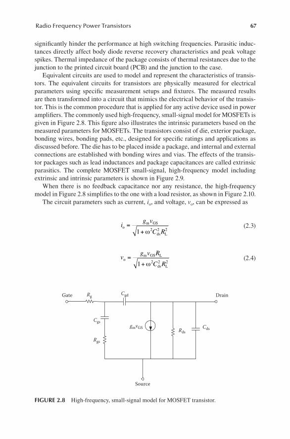
67Radio Frequency Power Transistors
significantly hinder the performance at high switching frequencies. Parasitic induc-tances directly affect body diode reverse recovery characteristics and peak voltage spikes. Thermal impedance of the package consists of thermal resistances due to the junction to the printed circuit board (PCB) and the junction to the case.
Equivalent circuits are used to model and represent the characteristics of transis-tors. The equivalent circuits for transistors are physically measured for electrical parameters using specific measurement setups and fixtures. The measured results are then transformed into a circuit that mimics the electrical behavior of the transis-tor. This is the common procedure that is applied for any active device used in power amplifiers. The commonly used high-frequency, small-signal model for MOSFETs is given in Figure 2.8. This figure also illustrates the intrinsic parameters based on the measured parameters for MOSFETs. The transistors consist of die, exterior package, bonding wires, bonding pads, etc., designed for specific ratings and applications as discussed before. The die has to be placed inside a package, and internal and external connections are established with bonding wires and vias. The effects of the transis-tor packages such as lead inductances and package capacitances are called extrinsic parasitics. The complete MOSFET small-signal, high-frequency model including extrinsic and intrinsic parameters is shown in Figure 2.9.
When there is no feedback capacitance nor any resistance, the high-frequency model in Figure 2.8 simplifies to the one with a load resistor, as shown in Figure 2.10.
The circuit parameters such as current, io, and voltage, vo, can be expressed as
ig v
C Ro
m GS
ds L
=+1 2 2 2ω
(2.3)
vg v R
C Ro
m GS L
ds L
=+1 2 2 2ω
(2.4)
Rg Cgd
Cgs
Rgs
RdsgmvGS Cds
Gate Drain
Source
FIGURE 2.8 High-frequency, small-signal model for MOSFET transistor.
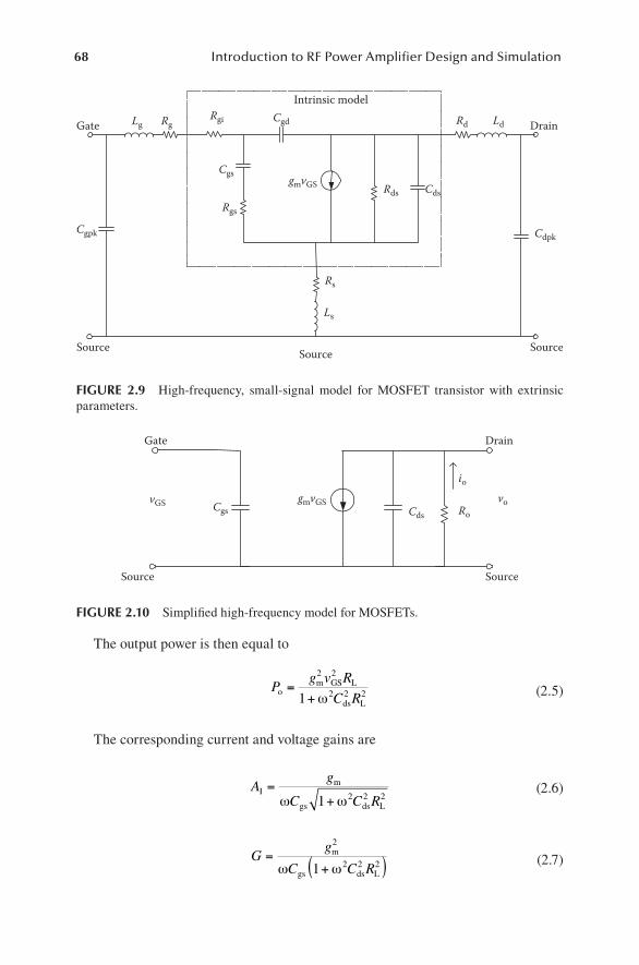
68 Introduction to RF Power Amplifier Design and Simulation
The output power is then equal to
Pg v R
C Ro
m GS L
ds L
=+
2 2
2 2 21 ω (2.5)
The corresponding current and voltage gains are
Ag
C C RI
m
gs ds L
=+ω ω1 2 2 2
(2.6)
Gg
C C R=
+( )m
gs ds L
2
2 2 21ω ω (2.7)
Drain
Source Source
Gate
Source
Lg RgRgi Cgd
Cgpk
Rgs
Rds Cds
Cdpk
gmvGSCgs
Rd Ld
Ls
Rs
Intrinsic model
FIGURE 2.9 High-frequency, small-signal model for MOSFET transistor with extrinsic parameters.
Gate Drain
Source Source
vGS Cgs Cds
gmvGSRo
io
vo
FIGURE 2.10 Simplified high-frequency model for MOSFETs.
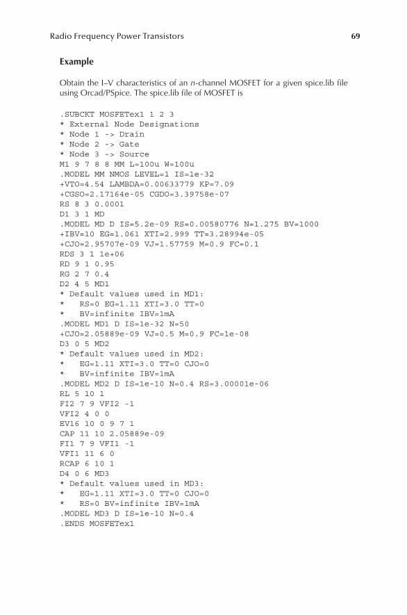
69Radio Frequency Power Transistors
Example
Obtain the I–V characteristics of an n-channel MOSFET for a given spice.lib file using Orcad/PSpice. The spice.lib file of MOSFET is
.SUBCKT MOSFETex1 1 2 3* External Node Designations* Node 1 -> Drain* Node 2 -> Gate* Node 3 -> SourceM1 9 7 8 8 MM L=100u W=100u.MODEL MM NMOS LEVEL=1 IS=1e-32+VTO=4.54 LAMBDA=0.00633779 KP=7.09+CGSO=2.17164e-05 CGDO=3.39758e-07RS 8 3 0.0001D1 3 1 MD.MODEL MD D IS=5.2e-09 RS=0.00580776 N=1.275 BV=1000+IBV=10 EG=1.061 XTI=2.999 TT=3.28994e-05+CJO=2.95707e-09 VJ=1.57759 M=0.9 FC=0.1RDS 3 1 1e+06RD 9 1 0.95RG 2 7 0.4D2 4 5 MD1* Default values used in MD1:* RS=0 EG=1.11 XTI=3.0 TT=0* BV=infinite IBV=1mA.MODEL MD1 D IS=1e-32 N=50+CJO=2.05889e-09 VJ=0.5 M=0.9 FC=1e-08D3 0 5 MD2* Default values used in MD2:* EG=1.11 XTI=3.0 TT=0 CJO=0* BV=infinite IBV=1mA.MODEL MD2 D IS=1e-10 N=0.4 RS=3.00001e-06RL 5 10 1FI2 7 9 VFI2 -1VFI2 4 0 0EV16 10 0 9 7 1CAP 11 10 2.05889e-09FI1 7 9 VFI1 -1VFI1 11 6 0RCAP 6 10 1D4 0 6 MD3* Default values used in MD3:* EG=1.11 XTI=3.0 TT=0 CJO=0* RS=0 BV=infinite IBV=1mA.MODEL MD3 D IS=1e-10 N=0.4.ENDS MOSFETex1
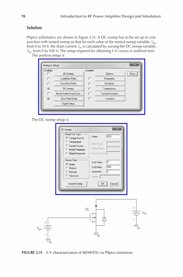
70 Introduction to RF Power Amplifier Design and Simulation
Solution
PSpice schematics are shown in Figure 2.11. A DC sweep has to be set up in con-junction with nested sweep so that for each value of the nested sweep variable, Vgs, from 0 to 10 V, the drain current, Id, is calculated by varying the DC sweep variable, Vds, from 0 to 100 V. The setup required for obtaining I–V curves is outlined next.
The analysis setup is
The DC sweep setup is
Q1Vds
+
–
0
0
+
–
0
Vgs
FIGURE 2.11 I–V characterization of MOSFETs via PSpice simulation.

71Radio Frequency Power Transistors
The nested sweep setup is
When simulation is run, the I–V characteristics are obtained from the Probe interface. As seen from simulation results shown in Figure 2.12, Vgs > Vth = 4.54 [V] as specified in the lib file that MOSFET conducts.
2.3 USE OF SIMULATION TO OBTAIN INTERNAL CAPACITANCES OF MOSFETs
2.3.1 Finding Ciss with PsPice
The Ciss given by Equation 2.1 for any MOSFET is obtained using the PSpice circuit given in Figure 2.13 by following the steps outlined below.
Vgs = 10 [V ]
Vgs = 9 [V ]
Vgs = 8 [V ]
Vgs = 7 [V ]
Vgs = 6 [V ]Vgs = 5 [V ]
I d (A
)
Vds (V)
100
80
60
40
20
0
120
0 5 10 15 20 25 30 35 40 45 50 55 60 65 70 75 80 85 90 95 100
FIGURE 2.12 PSpice simulation results for I–V curves of an enhancement MOSFET.
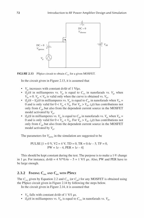
72 Introduction to RF Power Amplifier Design and Simulation
In the circuit given in Figure 2.13, it is assumed that
• Vgs increases with constant dv/dt of 1 V/μs.• |Ig(t)| in milliamperes vs. Vgs is equal to Ciss in nanofarads vs. Vgs when
Vds = 0. Vgs < Vth is valid only when the curve is obtained vs. Vds.• |Ig(t)| − |Id(t)| in milliamperes vs. Vgs is equal to Cgs in nanofarads when Vds =
0 and is only valid for 0 < Vgs < Vth. For Vgs > Vth, id(t) has contributions not only from Cgd but also from the dependent current source in the MOSFET model activated by Vgs.
• |Id(t)| in milliamperes vs. Vgs is equal to Cgd in nanofarads vs. Vgs when Vds = 0 and is only valid for 0 < Vgs < Vth. For Vgs > Vth, id(t) has contributions not only from Cgd but also from the dependent current source in the MOSFET model activated by Vgs.
The parameters for Vpulse in the simulation are suggested to be
PULSE [1 = 0 V, V2 = 4 V, TD = 0, TR = 0.4e – 5, TF = 0, PW = 1e – 4, PER = 1e – 4]
This should be kept constant during the test. The purpose is to make a 1-V change in 1 μs. For instance, dv/dt = 4 V/*0.4e – 5 = 1 V/1 μs. Also, PW and PER have to be large enough.
2.3.2 Finding Coss and Crss with PsPice
The Coss given by Equation 2.2 and Crss (or Cgd) for any MOSFET is obtained using the PSpice circuit given in Figure 2.14 by following the steps below.
In the circuit given in Figure 2.14, it is assumed that
• Vds falls with constant dv/dt of 1 V/1 μs.• |Id(t)| in milliamperes vs. Vds is equal to Coss in nanofarads vs. Vds.
+–
DC = 0Vigsense
DC = 0Vidsense
Vdd
Vg
–+
–+
– +
FIGURE 2.13 PSpice circuit to obtain Ciss for a given MOSFET.
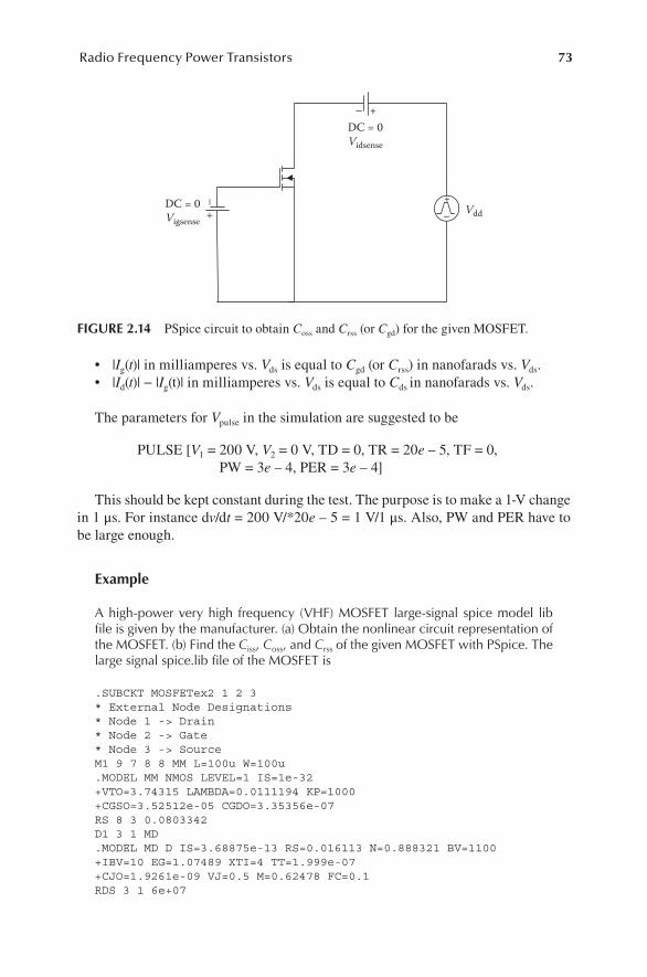
73Radio Frequency Power Transistors
• |Ig(t)| in milliamperes vs. Vds is equal to Cgd (or Crss) in nanofarads vs. Vds.• |Id(t)| − |Ig(t)| in milliamperes vs. Vds is equal to Cds in nanofarads vs. Vds.
The parameters for Vpulse in the simulation are suggested to be
PULSE [V1 = 200 V, V2 = 0 V, TD = 0, TR = 20e – 5, TF = 0, PW = 3e – 4, PER = 3e – 4]
This should be kept constant during the test. The purpose is to make a 1-V change in 1 μs. For instance dv/dt = 200 V/*20e – 5 = 1 V/1 μs. Also, PW and PER have to be large enough.
Example
A high-power very high frequency (VHF) MOSFET large-signal spice model lib file is given by the manufacturer. (a) Obtain the nonlinear circuit representation of the MOSFET. (b) Find the Ciss, Coss, and Crss of the given MOSFET with PSpice. The large signal spice.lib file of the MOSFET is
.SUBCKT MOSFETex2 1 2 3* External Node Designations* Node 1 -> Drain* Node 2 -> Gate* Node 3 -> SourceM1 9 7 8 8 MM L=100u W=100u.MODEL MM NMOS LEVEL=1 IS=1e-32+VTO=3.74315 LAMBDA=0.0111194 KP=1000+CGSO=3.52512e-05 CGDO=3.35356e-07RS 8 3 0.0803342D1 3 1 MD.MODEL MD D IS=3.68875e-13 RS=0.016113 N=0.888321 BV=1100+IBV=10 EG=1.07489 XTI=4 TT=1.999e-07+CJO=1.9261e-09 VJ=0.5 M=0.62478 FC=0.1RDS 3 1 6e+07
DC = 0Vigsense
DC = 0Vidsense
Vdd+–
–
–+
+
FIGURE 2.14 PSpice circuit to obtain Coss and Crss (or Cgd) for the given MOSFET.
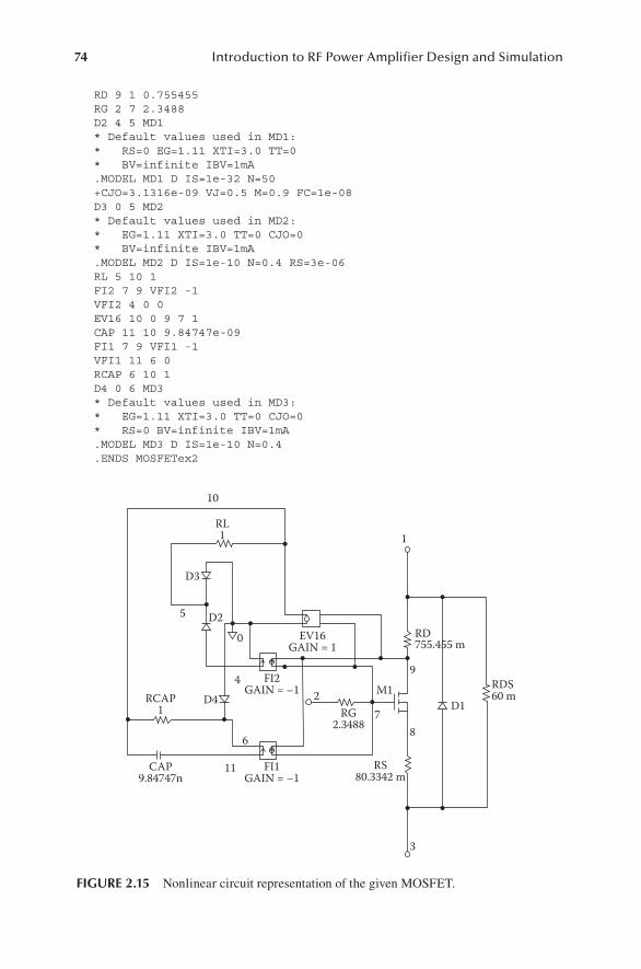
74 Introduction to RF Power Amplifier Design and Simulation
RD 9 1 0.755455RG 2 7 2.3488D2 4 5 MD1* Default values used in MD1:* RS=0 EG=1.11 XTI=3.0 TT=0* BV=infinite IBV=1mA.MODEL MD1 D IS=1e-32 N=50+CJO=3.1316e-09 VJ=0.5 M=0.9 FC=1e-08D3 0 5 MD2* Default values used in MD2:* EG=1.11 XTI=3.0 TT=0 CJO=0* BV=infinite IBV=1mA.MODEL MD2 D IS=1e-10 N=0.4 RS=3e-06RL 5 10 1FI2 7 9 VFI2 -1VFI2 4 0 0EV16 10 0 9 7 1CAP 11 10 9.84747e-09FI1 7 9 VFI1 -1VFI1 11 6 0RCAP 6 10 1D4 0 6 MD3* Default values used in MD3:* EG=1.11 XTI=3.0 TT=0 CJO=0* RS=0 BV=infinite IBV=1mA.MODEL MD3 D IS=1e-10 N=0.4.ENDS MOSFETex2
1
RDS60 m
RS80.3342 m
FI1GAIN = –1
FI2GAIN = –1
EV16GAIN = 1
CAP9.84747n
RCAP1
D4
4
0
D2
RL1
10
D3
5
11
6
RD755.455 m
9
8
3
D1M1
72
RG2.3488
FIGURE 2.15 Nonlinear circuit representation of the given MOSFET.
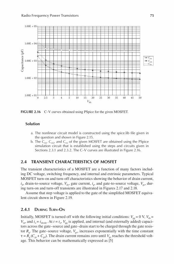
75Radio Frequency Power Transistors
Solution
a. The nonlinear circuit model is constructed using the spice.lib file given in the question and shown in Figure 2.15.
b. The Ciss, Coss, and Crss of the given MOSFET are obtained using the PSpice simulation circuit that is established using the steps and circuits given in Sections 2.3.1 and 2.3.2. The C–V curves are illustrated in Figure 2.16.
2.4 TRANSIENT CHARACTERISTICS OF MOSFET
The transient characteristics of a MOSFET are a function of many factors includ-ing DC voltage, switching frequency, and internal and extrinsic parameters. Typical MOSFET turn-on and turn-off characteristics showing the behavior of drain current, id, drain-to-source voltage, Vds, gate current, ig, and gate-to-source voltage, Vgs, dur-ing turn-on and turn-off transients are illustrated in Figures 2.17 and 2.18.
Assume that step voltage is applied to the gate of the simplified MOSFET equiva-lent circuit shown in Figure 2.19.
2.4.1 during turn-on
Initially, MOSFET is turned off with the following initial conditions: Vgg = 0 V, Vds = Vin, and io = idiode. At t = to, Vgg is applied, and internal (and externally added) capaci-tors across the gate–source and gate–drain start to be charged through the gate resis-tor Rg. The gate–source voltage, Vgs, increases exponentially with the time constant τ = Rg (Cgs + Cgd). The drain current remains zero until Vgs reaches the threshold volt-age. This behavior can be mathematically expressed as [5]
1.00E + 05
1.00E + 04
1.00E + 03
1.00E + 02
1.00E + 010 2.5 3 4 5 10 15 20
Vds
Capa
cita
nce (
pF)
25 30 35 40 45 50
CrssCossCiss
FIGURE 2.16 C–V curves obtained using PSpice for the given MOSFET.
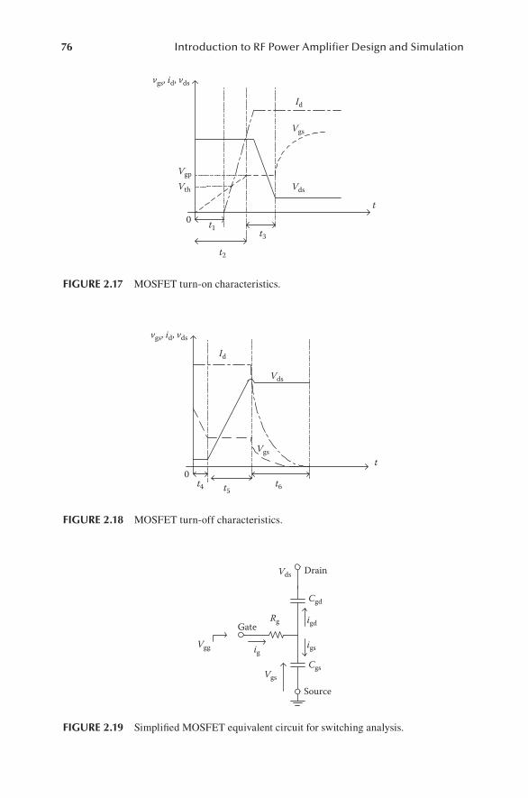
76 Introduction to RF Power Amplifier Design and Simulation
Id
Vds
Vgs
vgs, id, vds
t0
t4 t5t6
FIGURE 2.18 MOSFET turn-off characteristics.
Cgd
Cgs
Rg
Drain
Gate
Source
Vds
Vgg ig
igd
igs
Vgs
FIGURE 2.19 Simplified MOSFET equivalent circuit for switching analysis.
Id
Vds
Vgs
Vth
Vgp
vgs, id, vds
t0
t3t1
t2
FIGURE 2.17 MOSFET turn-on characteristics.
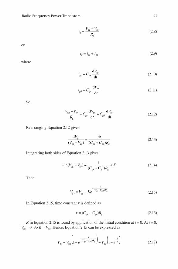
77Radio Frequency Power Transistors
iV V
Rggg gs
g
=−
(2.8)
or
ig = igs + igd (2.9)
where
i CV
tgs gsgsd
d= (2.10)
i CV
tgd gdgsd
d= (2.11)
So,
V V
RC
V
tC
V
tgg gs
ggs
gsgd
gsd
d
d
d
−= + (2.12)
Rearranging Equation 2.12 gives
d dgs
gg gs gs gd g
V
V Vt
C C R( ) ( )−=
+ (2.13)
Integrating both sides of Equation 2.13 gives
− − =+
+ln( )( )
V Vt
C C RKgg gs
gs gd g
(2.14)
Then,
V V K
t
C C Rgs gg
gs gd g= −−
+e ( ) (2.15)
In Equation 2.15, time constant τ is defined as
τ = (Cgs + Cgd)Rg (2.16)
K in Equation 2.15 is found by application of the initial condition at t = 0. At t = 0, Vgs = 0. So K = Vgg. Hence, Equation 2.15 can be expressed as
V V V
t
C C Rt
gs gg gggs gd g= −( ) = −( )−+ −
1 1e e( ) τ (2.17)
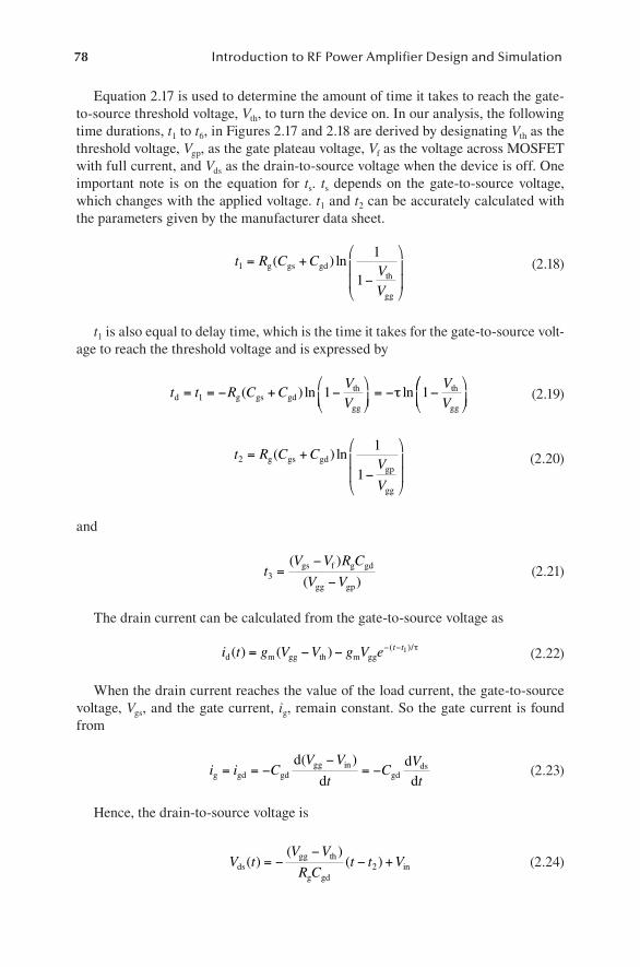
78 Introduction to RF Power Amplifier Design and Simulation
Equation 2.17 is used to determine the amount of time it takes to reach the gate-to-source threshold voltage, Vth, to turn the device on. In our analysis, the following time durations, t1 to t6, in Figures 2.17 and 2.18 are derived by designating Vth as the threshold voltage, Vgp, as the gate plateau voltage, Vf as the voltage across MOSFET with full current, and Vds as the drain-to-source voltage when the device is off. One important note is on the equation for ts. ts depends on the gate-to-source voltage, which changes with the applied voltage. t1 and t2 can be accurately calculated with the parameters given by the manufacturer data sheet.
t R C CVV
11
1= +
−
g gs gdth
gg
( ) ln (2.18)
t1 is also equal to delay time, which is the time it takes for the gate-to-source volt-age to reach the threshold voltage and is expressed by
t t R C CVV
VVd g gs gd
th
gg
th
gg
= = − + −
= − −1 1 1( ) ln lnτ
(2.19)
t R C CV
V
21
1
= +−
g gs gdgp
gg
( ) ln (2.20)
and
tV V R C
V V3 =−
−
( )
( )gs f g gd
gg gp
(2.21)
The drain current can be calculated from the gate-to-source voltage as
i t g V V g V e t td m gg th m gg( ) ( ) ( )/= − − − − 1 τ (2.22)
When the drain current reaches the value of the load current, the gate-to-source voltage, Vgs, and the gate current, ig, remain constant. So the gate current is found from
i i CV V
tC
Vtg gd gd
gg ingd
dsd
ddd
= = −−
= −( )
(2.23)
Hence, the drain-to-source voltage is
V tV V
R Ct t Vds
gg th
g gdin( )
( )( )= −
−− +2 (2.24)

79Radio Frequency Power Transistors
The dV/dt that happens during turn-on is an important parameter that impacts the performance of the amplifier. dV/dt can be calculated from Equation 2.23 as
dd
ds g
gd
Vt
i
C= − (2.25)
Substituting Equation 2.8 into Equation 2.25 gives
dd
ds g
gd
gg gs
g gd
Vt
i
C
V V
R C= − = −
− (2.26)
The value of the gate-to-source voltage, Vgs, in Equation 2.26 is calculated from the values given in the manufacturer data sheet for MOSFETs as
VIg
Vgso
mth= + (2.27)
So, the maximum value of dV/dt during turn-on is found from
dd
ds
g gdgg
o
mth
Vt R C
VIg
Vmax
= − +
1
(2.28)
2.4.2 during turn-oFF
The initial conditions for turn-off are Vds,onstate = RdsIo, ig = 0, Vgs = Vgg, and id = Io. The analysis performed during turn-on can be applied for derivation of the time duration turn-off. The transition time during turn-off is
t R C CV
V4 = +g gs gdgg
gp
( ) ln (2.29)
At the time t = t4, the gate-to-source and gate-to-drain capacitors discharge through Rg, and the gate current can be represented by
iV
Rggg
g
= − (2.30)
Also,
i i i C CV
tg gs gd gs gdgsd
d= + = +( ) (2.31)

80 Introduction to RF Power Amplifier Design and Simulation
which leads to
V V et
gs gg=−τ (2.32)
Vgs decreases until it reaches the constant value at the plateau, whereas the drain current, id, remains constant at id = Io. The gate-to-source voltage, Vgs, at id = Io is found from
VIg
Vgso
mth= + (2.33)
From Equations 2.32 and 2.33, we can obtain the time it takes for Vgs to reach the plateau voltage, or the constant value can be found as
VV
Ig
Vgs
gg
o
mth
=+
τ (2.34)
Time duration t5 can be calculated from
t R CV V
Vf
5 =−
g gd
ds
gp
ln (2.35)
Since Vgs is constant during t5, all the current at the gate is due to the gate-to-drain capacitance and can be expressed as
i Cv
tg gdgdd
d= (2.36)
or
i Cv v
tC
vtg gd
gs dsgd
dsd
ddd
=−
= −( )
(2.37)
Hence,
iR
Ig
Vgg
o
mth= +
1 (2.38)
From Equations 2.37 and 2.38, we can find the drain-to-source voltage as
V VR C
Ig
V t tds ds,ong gd
o
mth= + +
−
11( ) (2.39)
81Radio Frequency Power Transistors
The final time duration t6 is calculated from
t R C CV
V6 = +g gs gdgp
th
( ) ln (2.40)
When t6 begins, the free-wheeling diode in the MOSFET structure turns on, and the drain current starts falling. The drain current can then be represented as
id = gm(Vgs − Vth) (2.41)
where
VIg
V et t
gso
mth= +
−
−( )2τ (2.42)
The gate current during this cycle is found from
iR
Ig
V et t
gg
o
mth= − +
−
−1 2( )τ (2.43)
The turn-off time period is completed when the gate-to-source voltage becomes zero, Vgs = 0.
The MOSFET turn-on and turn-off times are illustrated in Figure 2.20. They can be related to the transition times defined by Equations 2.18 through 2.32 as follows. Turn-on delay time, td(on), is the time for the gate voltage, Vgs, to reach the threshold voltage, Vth. The input capacitance during this period is Ciss = Cgs + Cgd. This means that this is the charging period to bring up the capacitance to the threshold voltage.
It is expressed as
td(on) ≈ t1 + tir (2.44)
where tir is the current rise time and is defined by
tir = t2 − t1 (2.45)
or
t R Cg V V
g V V Iir g issm gg th
m gg th o
=−
− −
ln
( )
( ) (2.46)
Rise time is the period after Vgs reaches Vth to complete the transient. During the rise time, as both the high voltage and the high current exist in the device, high power dissipation occurs. The rise time should be reduced by reducing the gate series resistance and the drain–gate capacitance, Cgd. After this, the gate voltage continues

82 Introduction to RF Power Amplifier Design and Simulation
to increase up to the supplied voltage level, but as the drain voltage and the current are already in steady state, they are not affected during this region. Rise time can be expressed as
tr ≈ tvf (2.47)
where tvf is the voltage fall time and is defined by
tvf = t3 (2.48)
or
tQ V V R
V V V VIg
vfgd d ds f
ds d f d gg tho
m
=−
−( ) − +
_
_ _
( ) g
(2.49)
In Equation 2.49, (Vds_d − Vf_d) is the voltage swing at the drain of the MOSFET, and Qgd_d is the corresponding gate charge. Then, the MOSFET turn-on time, ton, is defined by
ton(MOSFET) = td(on) + tr (2.50)
Turn-off delay time, td(off), is the time for the gate voltage to reach the point where it is required to make the drain current become saturated at the value of the load current. During this time, there are no changes to the drain voltage and the cur-rent. It is defined by
td(off) ≈ t4 (2.51)
Vds Vgs
V
t0
td(on) td(off )
10%
90%
tr tf
FIGURE 2.20 Illustration of the MOSFET turn-on and turn-off times.

83Radio Frequency Power Transistors
where t4 is given in Equation 2.29. Then, MOSFET turn-off time is defined as
toff(MOSFET) = td(off) + tf (2.52)
where tf is the fall time where the gate voltage reaches the threshold voltage after td(off).
There is a lot of power dissipation in the tf region during the turn-off state similar to the turn-on state. Hence, tf must be reduced as much as possible. After this, the gate voltage continues to decrease until it reaches zero. As the drain voltage and the current are already in steady state, they are not affected during this region. tf is defined by
tf ≈ tvr (2.53)
where tvr is the voltage rise time and defined by
tvr = t5 (2.54)
or
tQ V V R
V V VIg
vrgd_d ds f g
ds_d f_d tho
m
=−
−( ) +
( ) (2.55)
The current fall time can also be expressed as
t R CV
Ig
Vif g iss
tho
m
th
=+
ln (2.56)
The rate change of current is calculated from
ddd d
if
it
it
= (2.57)
2.5 LOSSES FOR MOSFET
The power losses in MOSFETs are mainly due to conduction losses, Pc, and switch-ing losses, Psw [6–8]. Hence, the overall power loss for MOSFETs can be approxi-mated as
Ploss ≈ Pc + Psw (2.58)

84 Introduction to RF Power Amplifier Design and Simulation
The instantaneous value of the conduction losses for MOSFETs can be calculated using
P t V t i t R i tc d d ds d( ) ( ) ( ) ( )= = 2 (2.59)
The average value of the conduction loss in Equation 2.59 is calculated from
PT
P t tT
R i t t R I
T T
c c ds d ds dd d= = =∫ ∫1 1
0
2
0
2( ) ( ) (2.60)
where T represents the time period for switching. The switching loss for MOSFETs is
Psw = (Eon + Eoff)fsw (2.61)
where Eon and Eoff are the turn-on and turn-off energies for MOSFETs, respectively, and calculated from
E V t i t t V It t
Q V
t t
on d d dd donri fv
rr ddri fv
= =+
+
+
∫ ( ) ( )0
2 dd (2.62)
and
E V t i t t V It t
t t
on d d dd doffrv fid
rv fi
= =+
+
∫ ( ) ( )0
2 (2.63)
where Qrr is the reverse recovery charge. So the overall loss in MOSFETs from Equation 2.58 can be expressed as
P P P R I E E floss c sw dson drms on off sw= + = + +2 ( ) (2.64)
2.6 THERMAL CHARACTERISTICS OF MOSFETs
The thermal profile of MOSFETs is important in device performance. When power loss occurs, it is turned into heat and increases the junction temperature. This degrades the device characteristics and can cause device failure. As a result, it is crucial to lower the junction temperature by transferring heat from the chip junc-tion to ambient via the cold plate. The thermal path of MOSFETs illustrating die, case, junctions, cold plate, and ambient is shown in Figure 2.21. In the figure, Tj is used for junction temperature, Tc represents the case temperature at a point of the package that has the semiconductor die inside, Ts is used for heat sink or cold plate
85Radio Frequency Power Transistors
temperature, and Ta represents the ambient temperature of the surrounding environ-ment where the device is located. Rθjc shows the junction-to-case thermal resistance, Rθcs is used for the case-to-heat sink thermal resistance, and Rθsa shows the heat sink-to-ambient thermal resistance.
The heat produced at the die junction commonly radiates over 80% in the direc-tion of 1 and about 20% in the direction of 2, 3, and 4. The equivalent electrical circuit for the thermal path shown in Figure 2.21 is established and given in Figure 2.22. Thermal capacitance effect of the structure is ignored for simplicity of the analysis in Figure 2.22. Die junction-to-ambient thermal, Rθja, can be expressed as
Rθja = Rθjc + Rθcs + Rθsa (2.65)
In Equation 2.65, junction-to-case thermal resistance, Rθjc, is the internal thermal resistance from the die junction to the case package. If the size of the die is known, this thermal resistance of pure package is determined by the package design and lead frame material and is expressed by
RT T
Pθjcj c
d
[ C/W]=−
° (2.66)
D Case Tc
Heat sink Ts
Die Tj
G S
Ambient Ta
3
1
4
2Compound
FIGURE 2.21 Illustration of thermal path for MOSFETs.
Rθjc Rθcs Rθsa+
–
+
–
+
–
+
–
TjPd Tc Ts Ta
Junction Case Sink Ambient
FIGURE 2.22 Electrical equivalent circuit for thermal path.
86 Introduction to RF Power Amplifier Design and Simulation
Consider the power dissipation profile of MOSFETs shown in Figure 2.23 for a pulsing RF amplifier. The junction temperature varies accordingly and can be expressed as
Tjmax − Tc = RθjcPd (2.67)
The time-dependent thermal impedance for repetitive power pulses having a con-stant duty factor (D) is calculated using
Zθjc(t) = RθjcD + (1 − D)Sθjc(t) (2.68)
where Sθjc(t) is the thermal impedance for a single pulse. The drain current, Id, rating of the device is found from
I TT T
R T Rd Cjmax C
dson jmax jc
( )( )
=−
θ (2.69)
When MOSFETs are pulsed, the pulsed drain current rating is obtained from
Idpulse(Tc) = 4Id(Tc) (2.70)
The crossover point is an important point that identifies the safe operational region for MOSFETs. It is obtained by finding the intersection point of I–V curves of MOSFETs for extreme and nominal junction temperatures, Tj. The I–V charac-teristics of MOSFETs vs. junction temperature, Tj, giving the crossover point for MOSFETs are shown in Figure 2.24. MOSFETs are inherently stable when they are operated above the crossover point because hot spotting van occurs below the crossover point.
Pd
Pd (W )
Tj (°C )
11t
0
12tt
tt11 t12
0
Tj12Tj11
t2
FIGURE 2.23 Power dissipation profile and the corresponding junction temperature.
87Radio Frequency Power Transistors
2.7 SAFE OPERATING AREA FOR MOSFETs
Safe operating area (SOA) is the region identified by the maximum value of the drain-to-source voltage and drain current that guarantees safe operation when the device is at the forward bias. The SOA for MOSFETs can be expressed by a constant-power line, which is limited by thermal resistance with pulse width as a parameter. MOSFETs can be safely operated over a very wide range within the breakdown voltage between the drain and the source without narrowing the high-voltage area because secondary breakdown does not occur in the high-voltage area. The typical SOA for a MOSFET is illustrated in Figure 2.25. The relationship between SOA and device parameters such as Rdson and Pdmax is given in Figure 2.26. In Figure 2.26, the actual response of device dissipation characteristics, which has steeper slope when it is over a certain value, is assumed.
Id
Vgs
Vgs (Volts)
I d (A
mps
)
15
30
0
369
12
18212427
76
Crossoverpoint
Tj = –55°CTj = +25°CTj = +125°C
FIGURE 2.24 Transfer characteristics of MOSFETs vs. junction temperature, Tj.
100 (µs)1 (ms)
10 (ms)
* Single pulseat Tc = 25°C
maxdI
Vds
Id
Drain to source voltage (V)
Dra
in c
urre
nt (A
)
Vdmax
Idmax (pulsed)*
FIGURE 2.25 Typical SOA curves for MOSFETs.
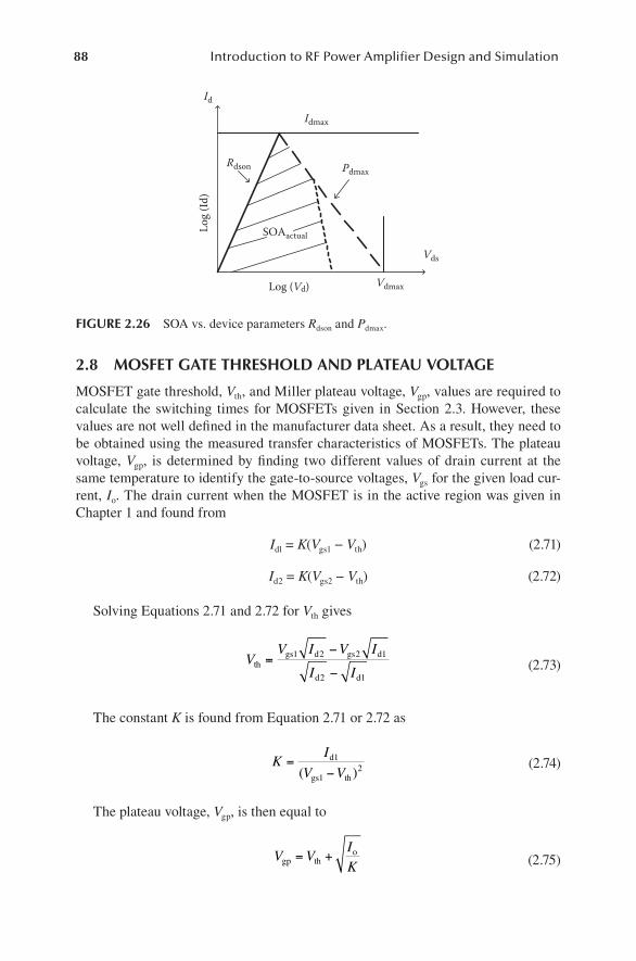
88 Introduction to RF Power Amplifier Design and Simulation
2.8 MOSFET GATE THRESHOLD AND PLATEAU VOLTAGE
MOSFET gate threshold, Vth, and Miller plateau voltage, Vgp, values are required to calculate the switching times for MOSFETs given in Section 2.3. However, these values are not well defined in the manufacturer data sheet. As a result, they need to be obtained using the measured transfer characteristics of MOSFETs. The plateau voltage, Vgp, is determined by finding two different values of drain current at the same temperature to identify the gate-to-source voltages, Vgs for the given load cur-rent, Io. The drain current when the MOSFET is in the active region was given in Chapter 1 and found from
Idl = K(Vgs1 − Vth) (2.71)
Id2 = K(Vgs2 − Vth) (2.72)
Solving Equations 2.71 and 2.72 for Vth gives
VV I V I
I Ith
gs d gs d1
d d1
=−
−1 2 2
2 (2.73)
The constant K is found from Equation 2.71 or 2.72 as
KI
V V=
−d1
gs th( )12 (2.74)
The plateau voltage, Vgp, is then equal to
V VIKgp tho= + (2.75)
Idmax
Pdmax
Vdmax
Vds
Id
Rdson
SOAactual
Log (Vd)
Log
(Id)
FIGURE 2.26 SOA vs. device parameters Rdson and Pdmax.
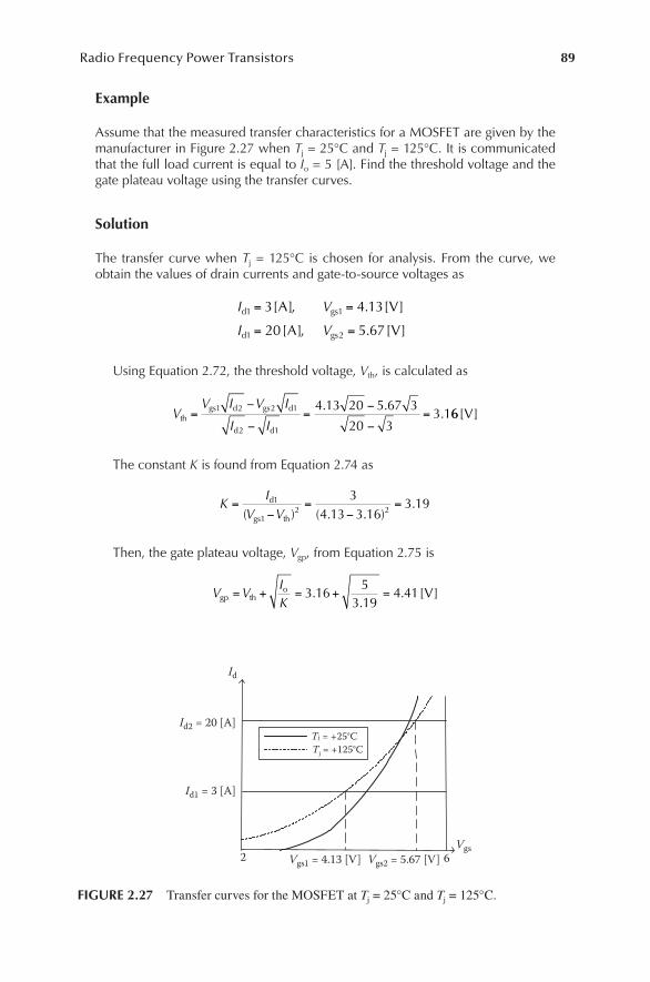
89Radio Frequency Power Transistors
Example
Assume that the measured transfer characteristics for a MOSFET are given by the manufacturer in Figure 2.27 when Tj = 25°C and Tj = 125°C. It is communicated that the full load current is equal to Io = 5 [A]. Find the threshold voltage and the gate plateau voltage using the transfer curves.
Solution
The transfer curve when Tj = 125°C is chosen for analysis. From the curve, we obtain the values of drain currents and gate-to-source voltages as
I V
I Vd gs
d gs
,
,1 1
1 2
3 4 13
20 5 67
= =
= =
[ ] . [ ]
[ ] . [ ]
A V
A V
Using Equation 2.72, the threshold voltage, Vth, is calculated as
VV I V I
I Ith
gs d gs d
d d
=−
−=
−
−=1 2 2 1
2 1
4 13 20 5 67 3
20 33 1
. .. 66[ ]V
The constant K is found from Equation 2.74 as
KI
V V=
−=
−=d
gs th
1
12 2
34 13 3 16
3 19( ) ( . . )
.
Then, the gate plateau voltage, Vgp, from Equation 2.75 is
V VIKgp tho= + = + =3 16
53 19
4 41..
. [ ]V
Id
Vgs2 6
Tj = +25°CTj = +125°C
Id2 = 20 [A]
Vgs1 = 4.13 [V ] Vgs2 = 5.67 [V ]
Id1 = 3 [A]
FIGURE 2.27 Transfer curves for the MOSFET at Tj = 25°C and Tj = 125°C.

90 Introduction to RF Power Amplifier Design and Simulation
PROBLEMS
1. Obtain the I–V characteristics of the MOSFET given in the example in Section 2.2 using ADS and MATLAB®/Simulink, and compare your results with the results obtained with PSpice in the example.
2. An RF amplifier used IRF440 MOSFET as an active device. It is rated for 500 V at 8 A with TO-3 package. The following information is given from the data sheet:
Rθcs = 0.2°C/W, Rθss = 1°C/W, Rθjc = 1°C/W
Rdson at 25°C = 0.8 Ω, Vgs = 10 V, Ta = 50°C, IDrms = 3 A, Pl = 5 W
Calculate the total die dissipation, Pt, and junction temperature, Tj, using the transient thermal model with
T T R P I R Rj a ja l D rms ds C dson= + + °θ ( ) ( )2
25
P P I R Rt l D rms ds C dson= + °( ) ( )2
25
and Rdson = 0.4 Ω at 67.3°C, Rdson = 2 Ω at 92.7°C. 3. The measurement of important parameters of a specific MOSFET has been
done, and the results obtained are tabulated in Table 2.1. Calculate the turn-on and turn-off times shown in Figure 2.20.
TABLE 2.1Measured Value of MOSFET Parameters
Min Type Max Unit
Rg 0.6 0.8 1 ΩRg_app 5.4 6 6.6 ΩCiss at Vds 620 775 930 pF
Ciss at 0 V 880 1100 1320 pF
gfs 21.6 27 32.4 S
Vgs_app 9 10 11 V
Vth 0.8 1.4 1.8 V
Ids 0.9 1 1.1 A
Qgd_d 2.8 3.5 4.2 nC
Vds_d 13.5 15 16.5 V
Ids_d 11.2 12.4 13.6 A
Rdson 0.008 0.01 0.012 ΩVf 0.0072 0.01 0.0132 V
Vf_d 0.09 0.12 0.16 V
Vds 13.5 15 16.5 V

91Radio Frequency Power Transistors
REFERENCES
1. B.J. Baliga. 2010. Advanced Power MOSFET Concepts. Springer, San Francisco. 2. M. Deboy, N. Marz, J.-P. Stengl, H. Strack, J. Tihanyi, and H. Weber. 1998. A new gen-
eration of high voltage MOSFETs breaks the limit line of silicon. IEDM ’98 Electron Devices Meeting, IEDM ’98, Technical Digest, pp. 683–685.
3. G. Sabui, and Z.J. Shen. 2014. On the feasibility of further improving Figure of Merits (FOM) of low voltage power MOSFETs. Proceedings of the 26th International Symposium on Power Semiconductor Devices & IC’s, June 15–19, Waikoloa, Hawaii.
4. S. Xu et al. 2009. NexFET: A new power device. Proceedings of the International Electron Devices Meeting, pp. 1–4.
5. B.J. Baliga. 1995. Power Semiconductor Devices. PWS Pub. Co, Boston. 6. M.H. Rashid. 2011. Power Electronics Handbook: Devices, Circuits, and Applications.
Academic Press, Burlington, MA. 7. N. Mohan. 1995. Power Electronics: Converters, Applications, and Design. John Wiley
and Sons, Hoboken, NJ. 8. D. Graovac, M. Pürschel, and A. Kiep. 2006. MOSFET Power Losses Calculation Using
the Data-Sheet Para meters. Infineon, Neubiberg, Germany.

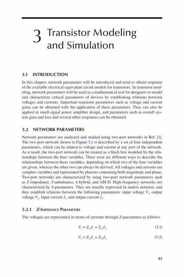
93
3 Transistor Modeling and Simulation
3.1 INTRODUCTION
In this chapter, network parameters will be introduced and used to obtain response of the available electrical equivalent circuit models for transistors. In transistor mod-eling, network parameters will be used as a mathematical tool for designers to model and characterize critical parameters of devices by establishing relations between voltages and currents. Important transistor parameters such as voltage and current gains can be obtained with the application of these parameters. They can also be applied in small-signal power amplifier design, and parameters such as overall sys-tem gain and loss and several other responses can be obtained.
3.2 NETWORK PARAMETERS
Network parameters are analyzed and studied using two-port networks in Ref. [1]. The two-port network shown in Figure 3.1 is described by a set of four independent parameters, which can be related to voltage and current at any port of the network. As a result, the two-port network can be treated as a black box modeled by the rela-tionships between the four variables. There exist six different ways to describe the relationships between these variables, depending on which two of the four variables are given, whereas the other two can always be derived. All voltages and currents are complex variables and represented by phasors containing both magnitude and phase. Two-port networks are characterized by using two-port network parameters such as Z-impedance, Y-admittance, h-hybrid, and ABCD. High-frequency networks are characterized by S-parameters. They are usually expressed in matrix notation, and they establish relations between the following parameters: input voltage V1, output voltage V2, input current I1, and output current I2.
3.2.1 Z-Impedance parameters
The voltages are represented in terms of currents through Z-parameters as follows:
V1 = Z11I1 + Z12I2 (3.1)
V2 = Z21I1 + Z22I2 (3.2)
94 Introduction to RF Power Amplifier Design and Simulation
In matrix form, Equations 3.1 and 3.2 can be combined and written as
V
V
Z Z
Z Z
I
I1
2
11 12
21 22
1
2
= (3.3)
The Z-parameters for a two-port network are defined as
ZV
IZ
V
I
ZV
IZ
V
I
I I
I I
111
1 0
121
2 0
212
1 0
222
2
2 1
2 1
= =
= =
= =
= =00
(3.4)
The formulation in Equation 3.4 can be generalized for an N-port network as
ZVI
I k m
nmn
mk
== ≠0( )
(3.5)
Znm is the input impedance seen looking into port n when all other ports are open circuited. In other words, Znm is the transfer impedance between ports n and m when all other ports are open. It can be shown that for reciprocal networks,
Znm = Zmn (3.6)
3.2.2 Y-admIttance parameters
The currents are related to voltages through Y-parameters as follows:
I1 = Y11V1 + Y12V2 (3.7)
I2 = Y21V1 + Y22V2 (3.8)
I1
+V1
I2
V2–
I2I1
+
–Two-port network
FIGURE 3.1 Two-port network representation.
95Transistor Modeling and Simulation
In matrix form, Equations 3.6 and 3.7 can be written as
I
I
Y Y
Y Y
V
V1
2
11 12
21 22
1
2
= (3.9)
The Y-parameters in Equation 3.9 can be defined as
YI
VY
I
V
YI
VY
I
V
V V
V V
111
1 0
121
2 0
212
1 0
222
2
2 1
2 1
= =
= =
= =
= =00
(3.10)
The formulation in Equation 3.10 can be generalized for an N-port network as
YIV
V k m
nmn
mk
== ≠0( )
(3.11)
Ynm is the input impedance seen looking into port n, when all other ports are short circuited. In other words, Ynm is the transfer admittance between ports n and m when all other ports are short. It can be shown that
Ynm = Ymn (3.12)
In addition, it can be further proved that the impedance and admittance matrices are related through
[Z] = [Y]−1 (3.13)
or
[Y] = [Z]−1 (3.14)
3.2.3 ABCD-parameters
ABCD-parameters relate the voltages to current in the following form for a two-port network:
V1 = AV1 − BI2 (3.15)
I1 = CV1 − DI2 (3.16)
96 Introduction to RF Power Amplifier Design and Simulation
which can be put in matrix form as
V
IA BC D
V
I1
1
1
2
=
−
(3.17)
The ABCD parameters in Equation 3.17 are defined as
AV
VB
V
I
CI
VD
I
I
I V
I V
= =−
= =−
= =
= =
1
2 0
1
2 0
1
2 0
1
2 0
2 2
2 2
(3.18)
It can be shown that
AD – BC = 1 (3.19)
for the reciprocal network and A = D for the symmetrical network. The ABCD net-work is useful in finding the voltage or current gain of a component or the overall gain of a network. One of the great advantages of ABCD parameters is their use in cas-caded network or components. When this condition exists, the overall ABCD param-eter of the network simply becomes the matrix product of an individual network and a component. This can be generalized for an N-port network shown in Figure 3.2 as
v
i
A B
C D
A B
C D1
1
1 1
1 1
=
… n n
n n
−
v
i2
2 (3.20)
3.2.4 h-HybrId parameters
Hybrid parameters relate voltage and current in a two-port network as
V1 = h11I1 + h12V2 (3.21)
I2 = h21I1 + h22V2 (3.22)
DnCn
BnAn
I2
V2 D1C1
B1A1
I1
V1
FIGURE 3.2 ABCD-parameter of cascaded networks.
97Transistor Modeling and Simulation
Equations 3.21 and 3.22 can be put in matrix form as
V
I
h h
h h
I
V1
2
11 12
21 22
1
2
= (3.23)
The hybrid parameters in Equation 3.23 can be found from
hV
I
hI
I
hV
V
hI
V
V
V
I
I
111
1 0
212
1 0
121
2 0
222
2
2
2
1
1
=
=
=
=
=
=
=,
==0
(3.24)
Hybrid parameters are preferred for components such as transistors and trans-formers since they can be measured with ease in practice.
Example
Obtain the h-parameter of the circuit shown in Figure 3.3 if L1 = L2 = M = 1 H.
Solution
There are two methods to solve this example.
• First method. From KVL on the primary side,
V sL I sMI1 1 1 2= +x (3.25)
Application of KCL gives
I I V1 1 1x = − (3.26)
1 [Ω]
+
V1
+
V2
I1 I2M
L1 L2
1 [Ω]
I1x
V2x
+
FIGURE 3.3 Coupling transformer example.
98 Introduction to RF Power Amplifier Design and Simulation
Substitution of I1x into the above equation gives
(1 + sL1)V1 − sMI2 = sL1I1 (3.27)
From KVL on the secondary side,
V V I2 2 2= +x (3.28)
Also,
V sL I sMI2 2 2 1x x= + (3.29)
Substitution of I1x
into the above leads to
V sL I sM I V2 2 2 1 1x = + −( ) (3.30)
When V2x
is inserted in V2, we obtain
V2 = (1 + sL2)I2 + sM(I1 − V1) (3.31)
or
sMV1 − (1 + sL2)I2 = sMI1 − V2 (3.32)
Equation 3.32 can be written in matrix form as
1
10
11
2
1
2
1+ −
− +
=
−
sL sM
SM sL
V
IsL
sM( )
I
V1
2 (3.33)
or
V
I
sL sM
sM sLsL
sM1
2
1
2
1
11
10
=
+ −
− +
−
( ) −−
1
1
2
I
V (3.34)
When L1 = L2 = M = 1 H, Equation 3.34 becomes
V
Is s
s sss
I1
2
1
11
01
= + −
− +
−
−
( )11
2V
(3.35)
or
V
I ss ss s
I
V1
2
1
2
12 1 1
=
+ − +
( ) (3.36)
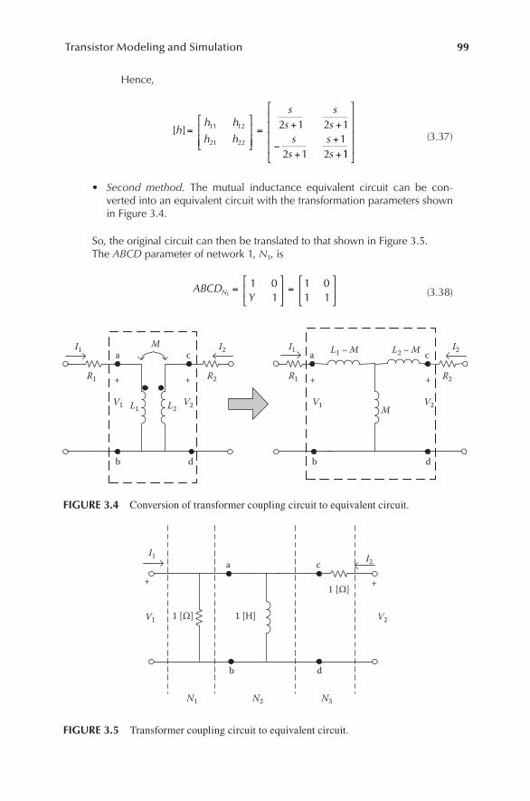
99Transistor Modeling and Simulation
Hence,
[ ]hh h
h h
ss
ss
ss
ss
=
= + +
−+
++
11 12
21 22
2 1 2 1
2 11
2 11
(3.37)
• Second method. The mutual inductance equivalent circuit can be con-verted into an equivalent circuit with the transformation parameters shown in Figure 3.4.
So, the original circuit can then be translated to that shown in Figure 3.5.The ABCD parameter of network 1, N1, is
ABCDY
N1
1 01
1 01 1
= = (3.38)
+
I1 I1 I2
R1 R1R2 R2
V1 V1 V2L1
L1 – M L2 – M
L2V2
I2M
+
a
b d
c
+
M
+
a
b d
c
FIGURE 3.4 Conversion of transformer coupling circuit to equivalent circuit.
1 [Ω]
I1 I2
V1 V2
N2 N3N1
1 [H]
a
b d
c
1 [Ω]+ +
FIGURE 3.5 Transformer coupling circuit to equivalent circuit.
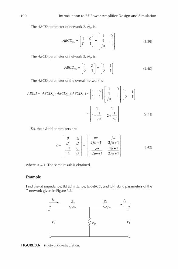
100 Introduction to RF Power Amplifier Design and Simulation
The ABCD parameter of network 2, N2, is
ABCDY j
N2
1 01
1 01
1=
=
ω
(3.39)
The ABCD parameter of network 3, N3, is
ABCD ZN3
10 1
1 10 1
= = (3.40)
The ABCD parameter of the overall network is
ABCD ABCD ABCD ABCDj
N N N= =
( )( )( )1 2 3
1 01 1
1 01
1ω
=+ +
1 10 1
1 1
11
21
j jω ω (3.41)
So, the hybrid parameters are
h
BD D
DCD
jj
jj
jj
j=
−
=+ +
−+
∆
1
2 1 2 1
2 1
ω
ω
ω
ω
ω
ω
ωω
ω
+
+
12 1j
(3.42)
where Δ = 1. The same result is obtained.
Example
Find the (a) impedance, (b) admittance, (c) ABCD, and (d) hybrid parameters of the T-network given in Figure 3.6.
I1
V1 V2ZC
ZA ZBI2
+ +
FIGURE 3.6 T-network configuration.
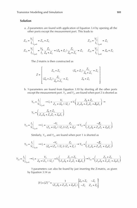
101Transistor Modeling and Simulation
Solution
a. Z-parameters are found with application of Equation 3.4 by opening all the other ports except the measurement port. This leads to
ZVI
Z Z ZVI
Z
ZVI
V
I I
I
111
1 0
212
1 0
121
2 0
2 2
1
= = + = =
= =
= =
=
A C C
22
222
2
2 01I
ZZ Z
Z ZZ
Z ZZ Z
VI
Z ZI
C
B CB C
C
B CC B C+
= ++
= = = +=
( )
The Z-matrix is then constructed as
ZZ Z Z Z
ZZ Z
Z
Z ZZ
Z ZZ Z Z
=
+ ++
=
++
= +
A C B CC
B CC
B CC
B CC B C
( )
( )
b. Y-parameters are found from Equation 3.10 by shorting all the other ports except the measurement port. Y11 and Y21 are found when port 2 is shorted as
YIV
IV
Z Z ZV
Z ZZ Z Z Z
V
111
1 0
11
1
2
= → =+
=+
+ += A B C
B C
A B A C( / / ) ZZ Z
YZ Z
Z Z Z Z Z Z
B C
B C
A B A C B C
→
=+
+ +
11
YIV
IV
Z Z ZZ
Z ZY
V
212
1 0
21
21
2
= → =−
+ +→ =
−
=( ( / / )) ( )A B C
C
C B
ZZZ Z Z Z Z Z
C
A B A C B C+ +
Similarly, Y12 and Y22 are found when port 1 is shorted as
YIV
IV
Z Z ZZ
Z ZY
V
121
2 0
12
12
1
= → =−
+ +→ =
−
=( ( / / )) ( )B A C
C
A C
ZZZ Z Z Z Z Z
C
A B A C B C+ +
YIV
IV
Z Z ZV
Z ZZ Z Z Z
V
222
2 0
22
1
1
= → =+
=+
+ += B A C
A C
A B A C( / / ) ZZ ZY
Z ZZ Z Z Z Z ZB C
A C
A B A C B C
→ =
++ +
22
Y-parameters can also be found by just inverting the Z-matrix, as given by Equation 3.14 as
[ ] [ ]( )
Y ZZ Z Z Z Z Z
Z Z Z
Z Z Z= =
+ +
+ −
− +
−1 1
A B A C B C
B C C
C A C

102 Introduction to RF Power Amplifier Design and Simulation
So, the Y-matrix for the T-network is then
Y
Z ZZ Z Z Z Z Z
ZZ Z Z Z Z Z
=
++ +
−
+ +
B C
A B A C B C
C
A B A C B C
−+ +
+
+ +
ZZ Z Z Z Z Z
Z ZZ Z Z Z Z Z
C
A B A C B C
A C
A B A C B C
As seen from the results of parts a and b, the network is reciprocal since
Z12 = Z21 and Y12 = Y21
c. Hybrid parameters are found using Equation 3.24. Parameters h11 and h21 are obtained when port 2 is shorted as
hVI
V I Z Z Z IZ Z Z Z Z Z
V
111
1 0
1 1 1
2
= → = + =+ +
=
( ( / / ))A B CA B A C B CC
B C
A B A C B C
B C
Z Zh
Z Z Z Z Z ZZ Z
+
→
=+ +
+
11
and
hII
I IZ
Z Zh
ZZ Z
V
212
1 0
2 1 21
2
= → = −+
→ = −
+
=
C
B C
C
B C
Parameters h12 and h22 are obtained when port 1 is open circuited as
hVV
V VZ
Z Zh
ZZ Z
I
121
1 0
1 2 12
1
= → =+
→ =
+
=
C
B C
C
B C
and
hIV
I VZ Z
hZ Z
I
222
2 0
2 2 22
1
1 1= → =
+
→ =
+
= B C B C
The hybrid matrix for the T-network can now be constructed as
h
Z Z Z Z Z ZZ Z
ZZ Z
ZZ Z
=
+ ++
+
−+
A B A C B C
B C
C
B C
C
B CC B C
+
1Z Z
103Transistor Modeling and Simulation
d. ABCD parameters are found using Equations 3.1 through 3.18. Parameters A and C are determined when port 2 is open circuited as
AVV
VZ
Z ZV A
Z ZZ
I
= → =+
→ =+
=
1
2 0
2 1
2
C
C A
C A
C
and
CIV
I VZ
CZ
I
= → =
→ =
=
1
2 0
1 2
2
1 1
C C
Parameters B and D are determined when port 2 is short circuited as
BVI
IV
Z Z ZZ
Z ZB
Z Z Z
V
=−
→ =−
+ +→ =
+
=
1
2 0
21
2A B C
C
B C
A B
( / / ) ( )AA C B C
C
Z Z ZZ
+
and
DII
I IZ
Z ZD
Z ZZ
V
=−
→ = −+
→ =
+
=
1
2 0
2 1
2
C
B C
B C
C
So, the ABCD matrix is
ABCD
Z ZZ
Z Z Z Z Z ZZ
Z
=
+ + +C A
C
A B A C B C
C
C
1 +Z ZZ
B C
C
It can be proven that Z, Y, h, and ABCD parameters are related using the rela-tions given in Table 3.1.
3.3 NETWORK CONNECTIONS
Networks and components in engineering applications can be connected in different ways to perform certain tasks. The commonly used network connection methods are series, parallel, and cascade connections. The series connection of two networks is shown in Figure 3.7. Since the networks are connected in series, currents are the same and voltages are added across ports of the network to find the overall voltage at the ports of the combined network. This can be represented by impedance matrices as
[ ] [ ] [ ]Z Z ZZ Z
Z Z
Z Z= + = +x y
x x
x x
y y11 12
21 22
11 12
ZZ Z
Z Z Z Z
Z Z Z21 22
11 11 12 12
21 21 2y y
x y x y
x y=
+ +
+ 22 22x y+ Z
(3.43)
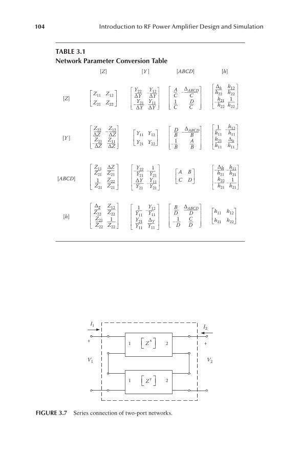
104 Introduction to RF Power Amplifier Design and Simulation
TABLE 3.1Network Parameter Conversion Table
Z11Y22 Y12 ∆ABCD
∆hh22
h12
h121h11
h11
h11h21h11
h22
∆h
∆Y
∆Z
1
1h21
h11h21
h22h21
h21h22
1h22
AC C
C1
CD
∆ABCDDB B
B1
BA
Y21∆Y
Z22∆Z
Z12∆Z
Z21∆Z
Z11∆Z
∆Y
∆Y∆YY11
∆h
Y121Y11
Y11
Y11
Y22Z11Z21 Z21
Z21
Z22Z21
Y21 Y21Y11Y21Y21
Y21Y11
∆Y
Z21
Z12
Z22
Y11
AC
BD
Y21
Y12
Y22
h11
h21
h12
h22
1h21
∆zZ22
Z12Z22
Z21Z22
1Z22
∆ABCDBD D
D1
DC
[Z]
[Z] [Y ] [ABCD] [h]
[Y ]
[ABCD]
[h]
1
1
2
2
I1
+ +
V1 V2
I2
Z x
Z y
FIGURE 3.7 Series connection of two-port networks.
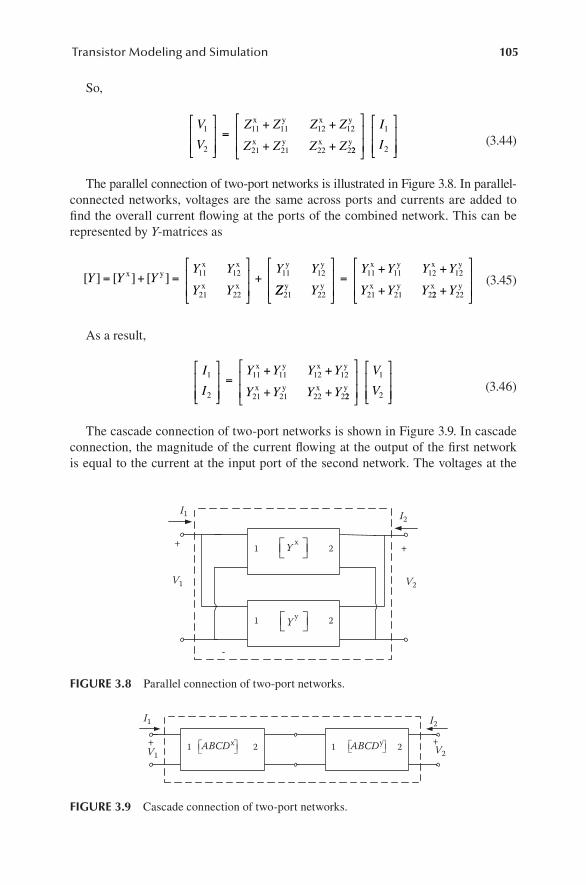
105Transistor Modeling and Simulation
So,
V
V
Z Z Z Z
Z Z Z Z
1
2
11 11 12 12
21 21 22 2
=+ +
+ +
x y x y
x y x22
1
2y
I
I (3.44)
The parallel connection of two-port networks is illustrated in Figure 3.8. In parallel-connected networks, voltages are the same across ports and currents are added to find the overall current flowing at the ports of the combined network. This can be represented by Y-matrices as
[ ] [ ] [ ]Y Y YY Y
Y Y
Y Y= + = +x y
x x
x x
y y11 12
21 22
11 12
ZZ Y
Y Y Y Y
Y Y Y21 22
11 11 12 12
21 21 2y y
x y x y
x y=
+ +
+ 22 22x y+Y
(3.45)
As a result,
I
I
Y Y Y Y
Y Y Y Y
1
2
11 11 12 12
21 21 22 2
=+ +
+ +
x y x y
x y x22
1
2y
V
V (3.46)
The cascade connection of two-port networks is shown in Figure 3.9. In cascade connection, the magnitude of the current flowing at the output of the first network is equal to the current at the input port of the second network. The voltages at the
1
1
2
2
I1
+ +
V1
I2
V2
Y x
Y y
FIGURE 3.8 Parallel connection of two-port networks.
1 12 2
I1
+ +V1
I2
V2ABCD x ABCD y
FIGURE 3.9 Cascade connection of two-port networks.
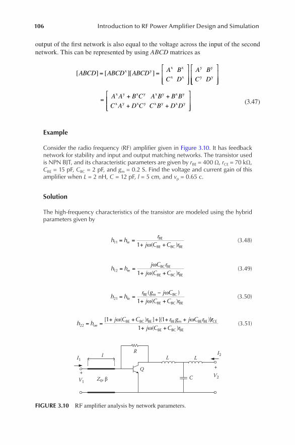
106 Introduction to RF Power Amplifier Design and Simulation
output of the first network is also equal to the voltage across the input of the second network. This can be represented by using ABCD matrices as
[ ] [ ][ ]ABCD ABCD ABCD A B
C D
A B
C D= =x y
x x
x x
y y
y y
= + +
+ +
A A B C A B B B
C A D C C B D D
x y x y x y x y
x y x y x y x y (3.47)
Example
Consider the radio frequency (RF) amplifier given in Figure 3.10. It has feedback network for stability and input and output matching networks. The transistor used is NPN BJT, and its characteristic parameters are given by rBE = 400 Ω, rCE = 70 kΩ, CBE = 15 pF, CBC = 2 pF, and gm = 0.2 S. Find the voltage and current gain of this amplifier when L = 2 nH, C = 12 pF, l = 5 cm, and vp = 0.65 c.
Solution
The high-frequency characteristics of the transistor are modeled using the hybrid parameters given by
h hr
j C C r11 1= =
+ +ieBE
BE BC BEω( ) (3.48)
h hj C r
j C C r12 1= =
+ +reBC BE
BE BC BE
ω
ω( ) (3.49)
h hr g j Cj C C r21 1
= =−
+ +feBE m BC
BE BC BE
( )( )
ω
ω (3.50)
h hj C C r r g j C r
221 1
= =+ + + + +
oeBE BC BE BE m BE BE[ ( ) ] [( )]ω ω rr
j C C rCE
BE BC BE1+ +ω( ) (3.51)
Z0, β
lR
Q
L L
C
I1
V1
++
I2
V2
FIGURE 3.10 RF amplifier analysis by network parameters.
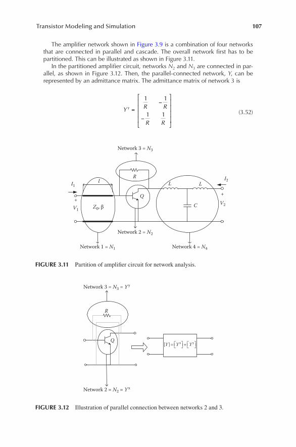
107Transistor Modeling and Simulation
The amplifier network shown in Figure 3.9 is a combination of four networks that are connected in parallel and cascade. The overall network first has to be partitioned. This can be illustrated as shown in Figure 3.11.
In the partitioned amplifier circuit, networks N2 and N3 are connected in par-allel, as shown in Figure 3.12. Then, the parallel-connected network, Y, can be represented by an admittance matrix. The admittance matrix of network 3 is
Y R R
R R
y =−
−
1 1
1 1 (3.52)
Z0, β
lR
Q
L L
C
I1
V1
++
I2
V2
Network 1 = N1 Network 4 = N4
Network 2 = N2
Network 3 = N3
FIGURE 3.11 Partition of amplifier circuit for network analysis.
R
Q[Y ] = +Y x Y y
Network 2 = N2 = Y x
Network 3 = N3 = Y y
FIGURE 3.12 Illustration of parallel connection between networks 2 and 3.
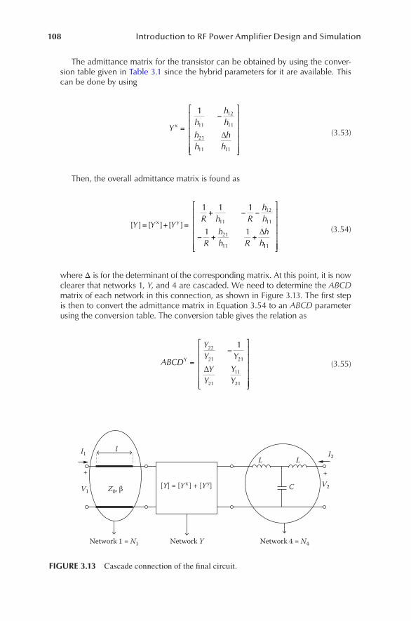
108 Introduction to RF Power Amplifier Design and Simulation
The admittance matrix for the transistor can be obtained by using the conver-sion table given in Table 3.1 since the hybrid parameters for it are available. This can be done by using
Yh
hh
hh
hh
x =
−
1
11
12
11
21
11 11
∆ (3.53)
Then, the overall admittance matrix is found as
[ ] [ ] [ ]Y Y YR h R
hh
Rhh R
hh
= + =
+ − −
− + +
x y
1 1 1
1 111
12
11
21
11
∆
111
(3.54)
where Δ is for the determinant of the corresponding matrix. At this point, it is now clearer that networks 1, Y, and 4 are cascaded. We need to determine the ABCD matrix of each network in this connection, as shown in Figure 3.13. The first step is then to convert the admittance matrix in Equation 3.54 to an ABCD parameter using the conversion table. The conversion table gives the relation as
ABCD
YY Y
YY
YY
Y
∆=
−
22
21 21
21
11
21
1
(3.55)
Network 1 = N1
Z0, β [Y] = [Y x ] + [Y y]
+
I1 I2l
L L
CV1
+V2
Network 4 = N4Network Y
FIGURE 3.13 Cascade connection of the final circuit.
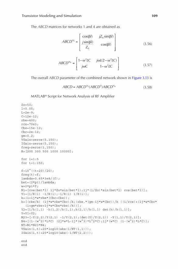
109Transistor Modeling and Simulation
The ABCD matrices for networks 1 and 4 are obtained as
ABCD
l jZ l
j lZ
lN1
0
0
=
cos( ) sin( )
sin( )cos( )
β β
ββ
(3.56)
ABCDLC j L LC
j C LCN4
1 2
1
2 2
2=
− −
−
ω ω ω
ω ω
( ) (3.57)
The overall ABCD parameter of the combined network shown in Figure 3.13 is
ABCD ABCD ABCD ABCDN N= 1 4( )Y (3.58)
MATLAB® Script for Network Analysis of RF Amplifier
Zo=50;l=0.05;L=2e-9;C=12e-12;rbe=400;rce=70e3;Cbe=15e-12;Cbc=2e-12;gm=0.2;VGain=zeros(5,150);IGain=zeros(5,150);freq=zeros(1,150);R=[200 300 500 1000 10000];
for i=1:5for t=1:150;
f=10^((t+20)/20);freq(t)=f;lambda=0.65*3e8/(f);bet=(2*pi)/lambda;w=2*pi*f;N1=[cos(bet*l) 1j*Zo*sin(bet*l);1j*(1/Zo)*sin(bet*l) cos(bet*l)];Y1=[1/R(i) -1/R(i);-1/R(i) 1/R(i)];k=(1+1j*w*rbe*(Cbc+Cbe));h= [(rbe/k) (1j*w*rbe*Cbc)/k;(rbe.*(gm-1j*w*Cbc))/k ((1/rce)+(1j*w*Cbc*(1+gm*rbe+1j*w*Cbe*rbe)/k))];
Y2=[1/h(1,1) -h(1,2)/h(1,1);h(2,1)/h(1,1) det(h)/h(1,1)];Y=Y1+Y2;N23=[-Y(2,2)/Y(2,1) -1/Y(2,1);(det(Y)/Y(2,1)) -Y(1,1)/Y(2,1)];N4=[(1-(w^2)*L*C) (2j*w*L-1j*(w^3)*L^2*C);1j*(w*C) (1-(w^2)*L*C)];NT=N1*N23*N4;VGain(i,t)=20*log10(abs(1/NT(1,1)));IGain(i,t)=20*log10(abs(-1/NT(2,2)));
endend
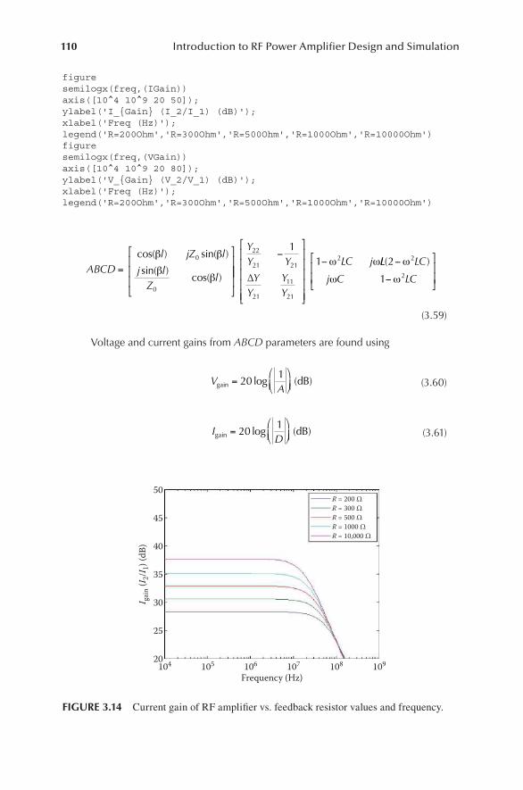
110 Introduction to RF Power Amplifier Design and Simulation
figuresemilogx(freq,(IGain))axis([10^4 10^9 20 50]);ylabel('I_Gain (I_2/I_1) (dB)');xlabel('Freq (Hz)');legend('R=200Ohm','R=300Ohm','R=500Ohm','R=1000Ohm','R=10000Ohm')figuresemilogx(freq,(VGain))axis([10^4 10^9 20 80]);ylabel('V_Gain (V_2/V_1) (dB)');xlabel('Freq (Hz)');legend('R=200Ohm','R=300Ohm','R=500Ohm','R=1000Ohm','R=10000Ohm')
ABCDl jZ l
j lZ
l=
cos( ) sin( )
sin( )cos( )
β β
ββ
0
0
−
−YY Y
YY
YY
LC j22
21 21
21
11
21
2
11
∆
ω ωLL LC
j C LC
( )2
1
2
2
−
−
ω
ω ω
(3.59)
Voltage and current gains from ABCD parameters are found using
VAgain dB= 201
log ( ) (3.60)
IDgain dB= 201
log ( ) (3.61)
50
45
40
35
30
25
20104 105 106 107
Frequency (Hz)
I gain
(I2/
I 1) (
dB)
108
R = 200 ΩR = 300 ΩR = 500 ΩR = 1000 ΩR = 10,000 Ω
109
FIGURE 3.14 Current gain of RF amplifier vs. feedback resistor values and frequency.
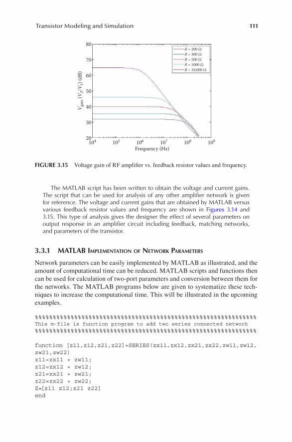
111Transistor Modeling and Simulation
The MATLAB script has been written to obtain the voltage and current gains. The script that can be used for analysis of any other amplifier network is given for reference. The voltage and current gains that are obtained by MATLAB versus various feedback resistor values and frequency are shown in Figures 3.14 and 3.15. This type of analysis gives the designer the effect of several parameters on output response in an amplifier circuit including feedback, matching networks, and parameters of the transistor.
3.3.1 mATLAB ImplementatIon of network parameters
Network parameters can be easily implemented by MATLAB as illustrated, and the amount of computational time can be reduced. MATLAB scripts and functions then can be used for calculation of two-port parameters and conversion between them for the networks. The MATLAB programs below are given to systematize these tech-niques to increase the computational time. This will be illustrated in the upcoming examples.
%%%%%%%%%%%%%%%%%%%%%%%%%%%%%%%%%%%%%%%%%%%%%%%%%%%%%%%%%%%%%%This m-file is function program to add two series connected network%%%%%%%%%%%%%%%%%%%%%%%%%%%%%%%%%%%%%%%%%%%%%%%%%%%%%%%%%%%%%%
function [z11,z12,z21,z22]=SERIES(zx11,zx12,zx21,zx22,zw11,zw12,zw21,zw22)z11=zx11 + zw11; z12=zx12 + zw12; z21=zx21 + zw21; z22=zx22 + zw22; Z=[z11 z12;z21 z22]end
80
70
60
50
40
30
20104 105 106 107
Frequency (Hz)
V gai
n (V 2
/V1)
(dB)
108
R = 200 ΩR = 300 ΩR = 500 ΩR = 1000 ΩR = 10,000 Ω
109
FIGURE 3.15 Voltage gain of RF amplifier vs. feedback resistor values and frequency.

112 Introduction to RF Power Amplifier Design and Simulation
%%%%%%%%%%%%%%%%%%%%%%%%%%%%%%%%%%%%%%%%%%%%%%%%%%%%%%%%%%%%%%This m-file is function program to add two parallel connected network%%%%%%%%%%%%%%%%%%%%%%%%%%%%%%%%%%%%%%%%%%%%%%%%%%%%%%%%%%%%%%
function [y11,y12,y21,y22]=PARALLEL(yx11,yx12,yx21,yx22,yw11,yw12,yw21,yw22)y11=yx11 + yw11 ;y12=yx12 + yw12 ;y21=yx21 + yw21 ;y22=yx22 + yw22 ;Y=[y11 y12;y21 y22]end
%%%%%%%%%%%%%%%%%%%%%%%%%%%%%%%%%%%%%%%%%%%%%%%%%%%%%%%%%%%%%%This m-file is function program to add two cascaded connected network%%%%%%%%%%%%%%%%%%%%%%%%%%%%%%%%%%%%%%%%%%%%%%%%%%%%%%%%%%%%%%
function [a11,a12,a21,a22]=CASCADE(ax11,ax12,ax21,ax22,aw11,aw12,aw21,aw22)a11=ax11.*aw11 + ax12.*aw21;a12=ax11.*aw12 + ax12.*aw22;a21=ax21.*aw11 + ax22.*aw21;a22=ax21.*aw12 + ax22.*aw22;A=[a11 a12;a21 a22]end
%%%%%%%%%%%%%%%%%%%%%%%%%%%%%%%%%%%%%%%%%%%%%%%%%%%%%%%%%%%%%%This m-file is function program to convert Z Parameters to Y Parameters%%%%%%%%%%%%%%%%%%%%%%%%%%%%%%%%%%%%%%%%%%%%%%%%%%%%%%%%%%%%%%
function [y11,y12,y21,y22]=Z2Y(z11,z12,z21,z22)DET=z11.*z22-z21.*z12;y11=z22./DET;y12=-z12./DET;y21=-z21./DET;y22=z11./DET;end
%%%%%%%%%%%%%%%%%%%%%%%%%%%%%%%%%%%%%%%%%%%%%%%%%%%%%%%%%%%%%%This m-file is function program to convert Y Parameters to Z Parameters%%%%%%%%%%%%%%%%%%%%%%%%%%%%%%%%%%%%%%%%%%%%%%%%%%%%%%%%%%%%%%
function [z11,z12,z21,z22]=Y2Z(y11,y12,y21,y22)DET=y11.*y22-y21.*y12;z11=y22./DET;z12=-y12./DET;z21=-y21./DET;z22=y11./DET;end

113Transistor Modeling and Simulation
%%%%%%%%%%%%%%%%%%%%%%%%%%%%%%%%%%%%%%%%%%%%%%%%%%%%%%%%%%%%%%This m-file is function program to convert Z Parameters to A Parameters%%%%%%%%%%%%%%%%%%%%%%%%%%%%%%%%%%%%%%%%%%%%%%%%%%%%%%%%%%%%%%
function [a11,a12,a21,a22]=Z2A(z11,z12,z21,z22)DET=z11.*z22-z21.*z12;a11=z11./z21;a12=DET./z21;a21=1./z21;a22=z22./z21;end
%%%%%%%%%%%%%%%%%%%%%%%%%%%%%%%%%%%%%%%%%%%%%%%%%%%%%%%%%%%%%%This m-file is function program to convert Y Parameters to A Parameters%%%%%%%%%%%%%%%%%%%%%%%%%%%%%%%%%%%%%%%%%%%%%%%%%%%%%%%%%%%%%%
function [a11,a12,a21,a22]=Y2A(y11,y12,y21,y22)DET=y11.*y22-y21.*y12;a11=-y22./y21;a12=-1./y21;a21=-DET./y21;a22=-y11./y21;end
The following MATLAB program uses the menu option and asks the user to enter the two-port network parameters when networks are connected in series or in paral-lel or are cascaded, and outputs the desired results.
%%%%%%%%%%%%%%%%%%%%%%%%%%%%%%%%%%%%%%%%%%%%%%%%%%%%%%%%%%%%%%This m-file is a script program that calculates the final 2-port% %parameters when networks are connected in series, parallel or cascaded%%%%%%%%%%%%%%%%%%%%%%%%%%%%%%%%%%%%%%%%%%%%%%%%%%%%%%%%%%%%%%clear;
M = menu('Network Analysis','2 Network in Series', '2 Network in Parallel','2-Network in Cascade');
switch M case 1 zx11 = input('enter Z1_11: '); zx12 = input('enter Z1_12: '); zx21 = input('enter Z1_21: '); zx22 = input('enter Z1_22: '); zw11 = input('enter Z2_11: '); zw12 = input('enter Z2_12: '); zw21 = input('enter Z2_21: '); zw22 = input('enter Z2_22: '); SERIES(zx11,zx12,zx21,zx22,zw11,zw12,zw21,zw22);
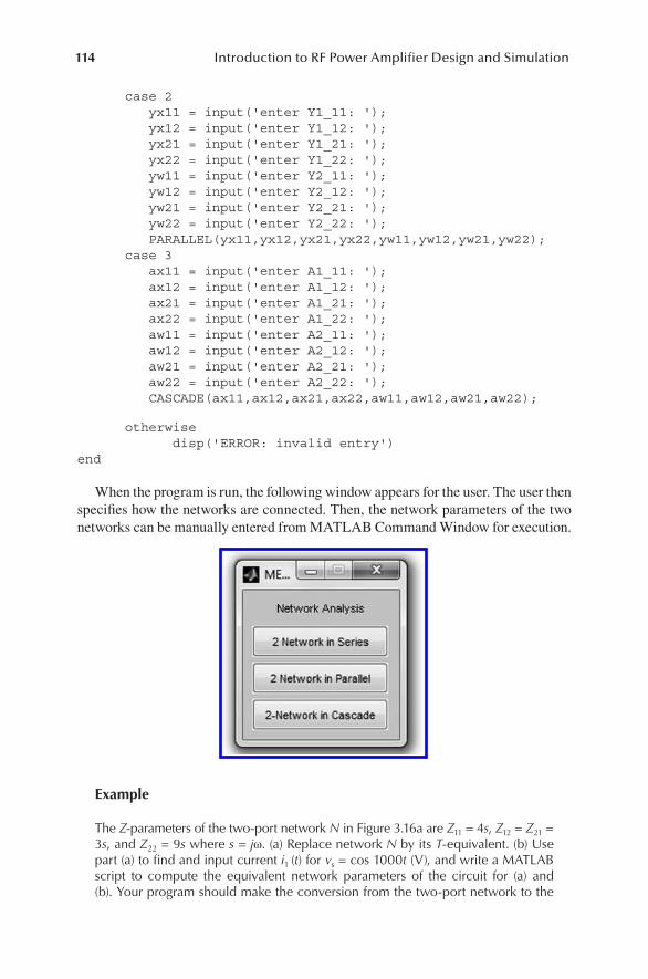
114 Introduction to RF Power Amplifier Design and Simulation
case 2 yx11 = input('enter Y1_11: '); yx12 = input('enter Y1_12: '); yx21 = input('enter Y1_21: '); yx22 = input('enter Y1_22: '); yw11 = input('enter Y2_11: '); yw12 = input('enter Y2_12: '); yw21 = input('enter Y2_21: '); yw22 = input('enter Y2_22: '); PARALLEL(yx11,yx12,yx21,yx22,yw11,yw12,yw21,yw22); case 3 ax11 = input('enter A1_11: '); ax12 = input('enter A1_12: '); ax21 = input('enter A1_21: '); ax22 = input('enter A1_22: '); aw11 = input('enter A2_11: '); aw12 = input('enter A2_12: '); aw21 = input('enter A2_21: '); aw22 = input('enter A2_22: '); CASCADE(ax11,ax12,ax21,ax22,aw11,aw12,aw21,aw22);
otherwise disp('ERROR: invalid entry')end
When the program is run, the following window appears for the user. The user then specifies how the networks are connected. Then, the network parameters of the two networks can be manually entered from MATLAB Command Window for execution.
Example
The Z-parameters of the two-port network N in Figure 3.16a are Z11 = 4s, Z12 = Z21 = 3s, and Z22 = 9s where s = jω. (a) Replace network N by its T-equivalent. (b) Use part (a) to find and input current i1 (t) for vs = cos 1000t (V), and write a MATLAB script to compute the equivalent network parameters of the circuit for (a) and (b). Your program should make the conversion from the two-port network to the
115Transistor Modeling and Simulation
T-equivalent network by checking if the two-port network is reciprocal. Execute your program, plot i(t), and confirm your results.
Solution
a. Any two networks can be converted to their equivalent T-network shown in Figure 3.16b if it is reciprocal.
The transformation of the network to the T-network shown in Figure 3.16b is valid with the following relations:
Z Z Z
Z Z Z
Z Z Z
a
b
c
= −
= −
= =
11 12
22 21
12 21
N
A+
B
V2V1+
C
I1
I1
I2
6 [kΩ]
12 [kΩ]Vs
N
A+
B
V2 V2V1V1+
I2I2I1 ZA ZB
ZC
++
I1
6 [kΩ]
Vs
s 6s
3s
12 [kΩ]
N
Zin
(a)
(b)
(c)
FIGURE 3.16 (a) N-network for analysis. (b) Network transformation to T-network. (c) Equivalent T-network.

116 Introduction to RF Power Amplifier Design and Simulation
Based on the given information, the network is reciprocal because Z12 = Z21. So, we can convert the network to its T-network equivalent and obtain
Z Z Z s s s
Z Z Z s s s
Z Z Z
a
b
c
= − = − =
= − = − =
= =
11 12
22 21
12 21
4 3
9 3 6
== 3s
Hence, this simplified network can now be analyzed by establishing the relations between voltage and current.
V Z I Z I
V Z I Z I
1 11 1 12 2
2 21 1 22 2
= +
= +
b. From the final circuit, we obtain Zin as
Z s V I ss s
ss jin s in/( )
( )( )= = +
+ ++
= + = + = ∠3 6 6 12
9 183 4 3 5 5 336 9. °
So, the current is
i(t) = 0.2cos(1000t − 36.9°) [mA]
This operation can be implemented by MATLAB simply.
%%%%%%%%%%%%%%%%%%%%%%%%%%%%%%%%%%%%%%%%%%%%%%%%%%%%%%%%%%%%%%This m-file is a script checks if a network is reciprocal network and then converts it to its equivalent T-network and calculates current%%%%%%%%%%%%%%%%%%%%%%%%%%%%%%%%%%%%%%%%%%%%%%%%%%%%%%%%%%%%%%clear;w = input('Circuit frequency: ');s=sqrt(-1)*w;
'Enter Z parameters for network N in figure 2:'z11 = input('Enter Z_11: ');z12 = input('Enter Z_12: ');z21 = input('Enter Z_21: ');z22 = input('Enter Z_22: '); if (z12==z21) za=z11-z12; zb=z22-z21; zc=z12; 'The T equivalent of network N is:' za zb zc zeq=((6000+zc)*(12000+zb))/((6000+zc)+(12000+zb))+za; t=0:0.0001:0.1; v=cos(1000*t);
117Transistor Modeling and Simulation
i=1/(abs(zeq))*cos(w*t-angle(zeq)); plot(t,i) title('i(t) for problem 2b'); xlabel('t'); ylabel('Amplitude'); else 'Network N is not reciprocal'end
Example
a. Obtain a small-signal model of the MOSFET using Y-parameters for the equivalent shown in Figure 3.17. (b) Use MATLAB to compute the voltage gain and phase of the voltage gain of the model when Rg = 5 Ω, Cgs = 10 × 10–12, Rgs = 0.5 Ω, Cgd = 100 × 10–12 F, Cds = 2 × 10–12 F, gm = 20 × 10–3 S, Rds = 70 × 103 Ω, RS = 3 Ω, RhighL = 10 × 103 Ω, and the connected load is RL = 10 × 103 Ω.
Solution
a. The equivalent circuit in Figure 3.17 is simplified and shown in Figure 3.18. When Figures 3.17 and 3.18 are compared, the following can be written:
Z R Z R jC
Z jCg g gs
gs gd
= = − = −, ,1 21 1
ω ω,
Z R Z R jC
Z R Z R ZZ ZZ Z3 4
3 4
3
1= = − = = ′ =
+ds highLds
s s L L, , , ,ω 44
Rg Cgd
Cgs
Rgs
Rds
Cds
Gate Drain
Source
gmVGS
RhighL
FIGURE 3.17 Small-signal MOSFET model.
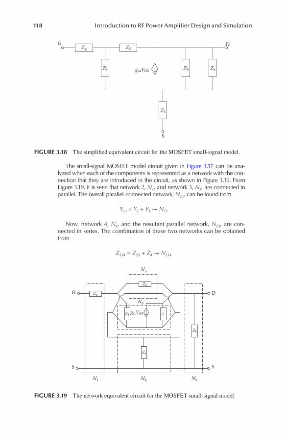
118 Introduction to RF Power Amplifier Design and Simulation
The small-signal MOSFET model circuit given in Figure 3.17 can be ana-lyzed when each of the components is represented as a network with the con-nection that they are introduced in the circuit, as shown in Figure 3.19. From Figure 3.19, it is seen that network 2, N2, and network 3, N3, are connected in parallel. The overall parallel-connected network, N23, can be found from
Y23 = Y2 + Y3 → N23
Now, network 4, N4, and the resultant parallel network, N23, are con-nected in series. The combination of these two networks can be obtained from
Z234 = Z23 + Z4 → N234
GZg
Zs
Z2
Z1 Z3 Z4gmVGS
D
S
FIGURE 3.18 The simplified equivalent circuit for the MOSFET small-signal model.
Zg
Zs
gmVGS Z
N1 N4
N3
N2
N5
G
S S
D
ZL
Z1
Z2
FIGURE 3.19 The network equivalent circuit for the MOSFET small-signal model.
119Transistor Modeling and Simulation
where Z23 = (Y23)−1. From Figure 3.19, it is also observed that networks, N1, N234, and N5 are cascaded. Hence, the overall network parameters can now be found from ABCD parameters:
[ ] [ ] [ ] [ ]ABCD ABCD ABCD ABCDN N NNetwork = 1 234 5
• The ABCD parameters for networks 1 and 5 and the Y parameters for network 2 are
[ ] ,[ ]ABCD
ZY
Y Y
Y YN N
C C
C C1 2
1
0 1=
=−
−g gd gd
gd gd
=
, [ ]and/
ABCDZN5
1 01 1L
• The Y-parameters for network 3 are found using Figure 3.20. The Y-parameters are found using Figure 3.20 as
YIV
Y YIV
YIV
g Y
V V
V
111
1 0
121
2 0
212
1 0
2
2 1
2
0= = = =
= =
= =
=
GS
m 222
2 0 31
1= =
=
IV Z
V
So,
[ ]YY
g ZN3
0
1=
′
GS
m /
• The parallel-connected network, N23, is now found from
[ ] [ ] [ ]Y Y Y
Y Y
Y YN N N
C C
C C23 3 2= + =
−
−
gd gd
gd gd
++′
Y
g ZGS
m /
0
1
ZGS gmVGS Z
+
VGS VL
+
I1 I2
FIGURE 3.20 The equivalent circuit for network 3.
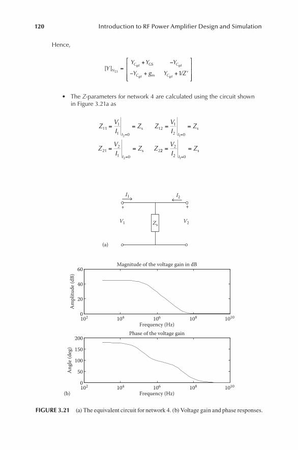
120 Introduction to RF Power Amplifier Design and Simulation
Hence,
[ ]Y
Y Y Y
Y g Y ZN
C C
C C23 1=
+ −
− + + ′
gd gd
gd gd
GS
m /
• The Z-parameters for network 4 are calculated using the circuit shown in Figure 3.21a as
ZVI
Z ZVI
Z
ZVI
Z Z
I I
I
111
1 0
121
2 0
212
1 0
2
2 1
2
= = = =
= =
= =
=
s s
s 222
2 01
= ==
VI
ZI
s
Zs
+ +
I1 I2
V2V1
102 104 106 108 1010
102 104 106 108 1010
0
20
40
60
Frequency (Hz)
Am
plitu
de (d
B)
Magnitude of the voltage gain in dB
0
50
100
150
200
Frequency (Hz)
Ang
le (d
eg)
Phase of the voltage gain
(a)
(b)
FIGURE 3.21 (a) The equivalent circuit for network 4. (b) Voltage gain and phase responses.

121Transistor Modeling and Simulation
So,
[ ]ZZ Z
Z ZN4= S S
S S
• The port parameters for series-connected networks N4 and N23 are found first by converting Y parameters for N23 to Z parameters by
[ ] ([ ] )Z Y
Y Z
Y
Y
Y
Y gN N
C
N
C
N
C23 23
23 231
1
= =
+ ′
−−
gd gd
gd
/
∆ ∆
mm GSgd
∆ ∆Y
Y Y
YN
C
N23 23
+
As a result, the two-port parameters for series-connected networks are found from
[ ] [ ] [ ]Z Z Z
Y Z
Y
Y
Y
YN N N
C
N
C
N
C234 23 4
23 23
1
= + =
+ ′gd gd
g
/
∆ ∆
dd gdm GS
S S
S− +
+g
Y
Y Y
Y
Z Z
Z Z
N
C
N∆ ∆23 23
SS
Hence,
[ ]Z
Y Z
YZ
Y
YZ
Y g
Y
N
C
N
C
N
C
N
234
23 23
1
=
+ ′+ +
−
gd gd
gd
/S S
m
∆ ∆
∆223 23
++
+
ZY Y
YZ
C
NS
GS
Sgd
∆
• We need to convert the resultant central Z parameters to ABCD param-eters using
[ ]
( )
( )
[ ]
( )[ ]
[ ]ABCD
Z
Z
Z
ZN
Z
Z
NN
N
234
234
234
23411
21 21=
[[ ]
[ ]
[ ]
[ ]( )
( )
( )
Z
Z
Z
Z
N
N
N
NZ
Z
Z
234
234
234
234
1
21
22
21
• The complete network parameters of the small-signal model of MOSFETs are found from ABCD parameters since now, N1, N234, and N5 are all cascaded as
[ ] [ ] [ ] [ ]ABCD ABCD ABCD ABCDN N N=1 234 5

122 Introduction to RF Power Amplifier Design and Simulation
or
[ ]
( )
( )
[ ][ ]
[ ]ABCD
Z
Z
Z
ZZ
Z
N
N=1
0 1
11
21
234
234g
NN
Z
Z
Z
Z
Z
Z
Z
N
N
N
234
234
234
234
21
21
22
21
1
( )
( )
( )
( )
[ ]
[ ]
[ ]
[[ ]Z N
Z
234
1 01 1/ L
b. The MATLAB script is written to obtain the characteristics of the network by finding the voltage gain and the phase of the voltage gain using the MATLAB functions developed and given in Section 3.4, as shown below.
%%%%%%%%%%%%%%%%%%%%%%%%%%%%%%%%%%%%%%%%%%%%%%%%%%%%%%%%%%%%%%%%%%%%%%This m-file is developed to calculate the response of small signal MOSFET model%%%%%%%%%%%%%%%%%%%%%%%%%%%%%%%%%%%%%%%%%%%%%%%%%%%%%%%%%%%%%%%%%%%%%%
clearRg=5;Cgs=10e-12;rgs=0.5;Cgd=100e-12;Cds=2e-12;Gm=20e-3;Rds=70e3;RL=10e3;RS=3;Rhigh=10e3;f=logspace(3,10);omega=2*pi.*f;Z3=Rds;Z4=1./(1i.*omega.*Cds)+Rhigh;Zp=(Z3.*Z4)./(Z3+Z4);
%+++++++++++++++++++++++++VCCS (y-parameters)+++++++++++++++++++++++++VCCS_11=1./(rgs.*ones(size(f))+1./(1i.*omega.*Cgs));VCCS_12=zeros(size(f));VCCS_21=Gm.*ones(size(f));VCCS_22=1./(Zp);%+++++++++++++++++++++++++CGD (y-parameters)++++++++++++++++++++++++++CGD_11= 1i.*omega.*Cgd;CGD_12=-1i.*omega.*Cgd;CGD_21=-1i.*omega.*Cgd;CGD_22= 1i.*omega.*Cgd;%++++++++++++++++++++++++++RS (z-parameters)++++++++++++++++++++++++++RS_11=RS.*ones(size(f));RS_12=RS.*ones(size(f));RS_21=RS.*ones(size(f));RS_22=RS.*ones(size(f));%++++++++++++++++++++++++RL (ABCD-parameters)+++++++++++++++++++++++++RL_11=1.*ones(size(f));RL_12=0.*ones(size(f));RL_21=1./(RL);RL_22=1.*ones(size(f));

123Transistor Modeling and Simulation
%++++++++++++++++++++++++Ci (ABCD-parameters)+++++++++++++++++++++++++Ci_11=1.*ones(size(f));Ci_12=(Rg.*ones(size(f)));Ci_21=0.*ones(size(f));Ci_22=1.*ones(size(f));%++++++++++++++++++++++++++++Xa = VCCS and CGD++++++++++++++++++++++++[Xa _11,Xa_12,Xa_21,Xa_22]=PARALLEL(VCCS_11,VCCS_12,VCCS_21,VCCS_22,
CGD _11,CGD_12,CGD_21,CGD_22);%++++++++++++++++++++Convert Admittance to Impedance++++++++++++++++++[z11,z12,z21,z22]=Y2Z(Xa_11,Xa_12,Xa_21,Xa_22);%+++++++++++++++++++++++Xb = VCCS, CGD and RS+++++++++++++++++++++++++[Xb _11,Xb_12,Xb_21,Xb_22]=SERIES(z11,z12,z21,z22,RS_11,RS_12,RS_21,
RS_22);%+++++++++++++++++++++Convert Impedance to ABCD+++++++++++++++++++++++[a11,a12,a21,a22]=Z2A(Xb_11,Xb_12,Xb_21,Xb_22);%++++++++++++++++++++++Xc = VCCS, CGD, RS and RL++++++++++++++++++++++[Xc _11,Xc_12,Xc_21,Xc_22]=CASCADE(a11,a12,a21,a22,RL_11,RL_12,RL_21,
RL_22);%++++++++++++++++++++Xd = VCCS, CGD, RS, RL and Ci++++++++++++++++++++[Xd _11,Xd_12,Xd_21,Xd_22]=CASCADE(Xc_11,Xc_12,Xc_21,Xc_22,Ci_11,Ci_12,
Ci_21,Ci_22);subplot(211)semilogx(f,20*log10(abs(1./Xd_11)))xlabel('Frequency (Hz)')ylabel('Amplitude (dB)')title('Magnitude of the voltage gain in dB')subplot(212)semilogx(f,((angle(1./Xd_11)).*180)./pi)xlabel('Frequency (Hz)')ylabel('Angle (deg)')title('Phase of the voltage gain')%=====================================================================
The voltage gain and phase responses when the program is run are given in Figure 3.21b.
3.4 S-SCATTERING PARAMETERS
Scattering parameters are used to characterize RF/microwave devices and compo-nents at high frequencies [2]. Specifically, they are used to define the return loss and insertion loss of a component or a device.
3.4.1 one-port network
Consider the circuit given in Figure 3.22. The relationship between current and volt-age can be written as
IV
Z Z=
+g
g L (3.62)
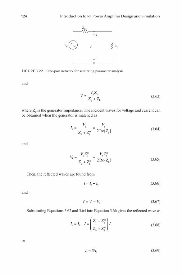
124 Introduction to RF Power Amplifier Design and Simulation
and
VV Z
Z Z=
+g L
g L (3.63)
where Zg is the generator impedance. The incident waves for voltage and current can be obtained when the generator is matched as
IV
Z Z
V
Zig
g g
g
g
=+ ∗
=2Re (3.64)
and
VV Z
Z Z
V Z
Zig g
g g
g g
g
=∗
+ ∗=
∗
2Re (3.65)
Then, the reflected waves are found from
I = Ii − Ir (3.66)
and
V = Vi − Vr (3.67)
Substituting Equations 3.62 and 3.64 into Equation 3.66 gives the reflected wave as
I I IZ Z
Z ZIr i
L g
L g
i= − =− ∗
+ ∗
(3.68)
or
Ir = SIIi (3.69)
Vg
Zg
ZLV
+
FIGURE 3.22 One-port network for scattering parameter analysis.
125Transistor Modeling and Simulation
where
SZ Z
Z Z
I L g
L g
=− ∗
+ ∗
(3.70)
is the scattering matrix for current. A similar analysis can be done to find the reflected voltage wave by substituting Equations 3.63 and 3.65 into Equation 3.67 as
V V VZ
Z
Z Z
Z ZVr i
g
g
L g
L g
i= − =∗
− ∗
+ ∗
(3.71)
or
VZ
ZS V S Vr
g
g
Ii
Vi=
∗= (3.72)
where
SZ
ZSV g
g
I=∗
(3.73)
is the scattering matrix for voltage. It can also be shown that
V Z Ii g i= ∗ (3.74)
Vr = ZgIr (3.75)
When the generator impedance is purely real, Zg = Rg, then
S SZ R
Z RI V L g
L g i
= =−
+
(3.76)
3.4.2 N-port network
The analysis described in Section 3.4.1 can be extended to the N-port network shown in Figure 3.23. The analysis is based on the assumption that generators are indepen-dent of each other. Hence, the Z-generator matrix has no cross-coupling terms, and it can be expressed as a diagonal matrix:
126 Introduction to RF Power Amplifier Design and Simulation
[ ]Z
Z
Z
Z
g
g
g
gn
=
1
2
0 0
0 0
0 0
…
(3.77)
From Equations 3.66 and 3.67, the incident and reflected waves are related to the actual voltage and current values as
[I] = [Ii] − [Ir] (3.78)
[V] = [Vi] + [Vr] (3.79)
From Equations 3.74 and 3.75, the incident and reflected components can be related through
[ ] [ ][ ]V Z Ii g i= ∗ (3.80)
[Vr] = [Zg][Ir] (3.81)
Vg1
Zg1
V1
+
N-port network
Vg4
Zg1
+
Vgn
Zgn+ +
V4
V5 V8
+
+
Vn
V9Vg9
Z9
Vg5 Vg8
Zg5 Zg8
I1
I4
I5 I8
I9
In
FIGURE 3.23 N-port network for scattering analysis.
127Transistor Modeling and Simulation
similar to the one-port case as derived before. For the N-port network, Z parameters can be obtained as
[V] = [Z][I] (3.82)
Using Equations 3.77 through 3.82, we can obtain
[ ] [ ] [ ] [ ][ ] [ ][ ]V V V Z I Z Ir i g i= − = − ∗ (3.83)
Equation 3.83 can also be expressed as
[ ][ ] [ ][ ] [ ][ ] [ ]([ ] [ ]) [ ][Z I Z I Z I Z I I Zg r g i i r g= − ∗ = − − ∗ II i ] (3.84)
and simplified to
([ ] [ ])[ ] ([ ] [ ])[ ]Z Z I Z Z I+ = − ∗g r g i (3.85)
Equation 3.85 can be put in the following form:
[ ] ([ ] [ ]) ([ ] [ ])[ ]I Z Z Z Z Ir g g i= + − ∗−1 (3.86)
From Equation 3.70, the scattering matrix for the current for the N-port network is equal to
S Z Z Z ZIg g= + − ∗−([ ] [ ]) ([ ] [ ])1
(3.87)
Then, Equation 3.86 can be expressed as
[Ir] = [SI][Ii] (3.88)
For the N-port network, the Y parameters for the short-circuit case can be obtained similarly as
[I] = [Y][V] (3.89)
It can also be shown that
[ ] ([ ] [ ]) ([ ] [ ])[ ]V Y Y Y Y Vr g g i= − + − ∗−1 (3.90)
or
[Vr] = [SV][Vi] (3.91)
128 Introduction to RF Power Amplifier Design and Simulation
where
S Y Y Y YVg g= − + − ∗−([ ] [ ]) ([ ] [ ])1
(3.92)
Example
Consider a transistor network that is represented as a two-port network and con-nected between the source and the load. It is assumed that the generator or source and load impedances are equal and given to be Rg. The transistor is represented by the following Z parameters, as shown in Figure 3.24. Find the current scattering matrix, SI.
[ ]ZZ Z
Z Z= i r
f o
Solution
From Equation 3.87, the scattering matrix for current is
S Z Z Z ZIg g= + − ∗−([ ] [ ]) ([ ] [ ])1
(3.93)
The generator Zg-matrix is
[ ] [ *]Z ZR
Rg gg
g
= =0
0 (3.94)
Then,
[ ] [ ]Z ZZ Z
Z Z
R
R
Z R+ ∗ =
+
=
+g
i r
f o
g
g
i g0
0
00
0 Z Ro g+
(3.95)
Vg
Zg
ZLV
+
Zi Zr
Zf Zo
I
FIGURE 3.24 Two-port transistor network.

129Transistor Modeling and Simulation
The inverse of the matrix in Equation 3.95 is
[([ ] [ ])][ ] [ ]
([[ ] [ ]] )Z ZZ Z
Z Z+ ∗ =+ ∗
+ ∗−g
g
gC T1 1
(3.96)
[ ] [ ]Z Z+ ∗g is the determinant of [ ] [ ]Z Z+ ∗
g and is calculated as
[ ] [ ] ( )( )Z Z Z R Z R Z Z+ ∗ = + + −g i g o g r f (3.97)
[[ ] [ ]]Z Z+ ∗g
C
is the cofactor matrix for [ ] [ ]Z Z+ ∗g and is calculated as
([ ] [ ])Z ZZ R Z
Z Z R+ ∗ =
+ −
− +
g
C o g f
r i g (3.98)
Then,
[([ ] [ ]) ]Z ZZ R Z
Z Z R+ ∗ =
+ −
− +
g
C T o g r
f i g (3.99)
Hence, the inverse of the matrix from Equations 3.97 through 3.99 is equal to
[([ ] [ ])](( )( ) )
Z ZZ R Z R Z Z
Z R Z+ ∗ =
+ + −
+ −
−−
gi g o g r f
o g r1 1ZZ Z Rf i g+
(3.100)
Then, from Equation 3.93,
S Z Z Z ZZ R Z R Z Z
Ig g
i g o g r f
= + − =+ + −
−([ ] [ ]) ([ ] [ ])(( )( )
1 1))
Z R Z
Z Z R
Z R Z
o g r
f i g
i g
+ −
− +
−− rr
f o gZ Z R−
(3.101)
which can be simplified to
S Z Z Z ZZ R Z R Z Z Z
Ig g
o g i g r f= + − =
+ − −−([ ] [ ]) ([ ] [ ])
( )( )1
2 rr g
f g i g o g r f
R
Z R Z R Z R Z Z2 ( )( )+ − −
(3.102)
130 Introduction to RF Power Amplifier Design and Simulation
3.4.3 normalIzed scatterIng parameters
Normalized scattering parameters can be introduced by Equations 3.103 and 3.104 for the incident and reflected waves as follows:
[ ] ([ ] [ *])[ ]a Z Z I= +1
2g g i (3.103)
[ ] ([ ] [ *])[ ]b Z Z I= +1
2g g r (3.104)
where
1
2
0 0
0 0
0 0
1
2([ ] [ *]) Re
Re
Re Z Z Z
Z
Zg g g
g
g+ = =
…
Re Zgn
(3.105)
Substituting Equation 3.86 into Equations 3.103 and 3.104 gives
[ ]
Re [ ] [ ][ ]
b
ZI S I
g
rI
i= = (3.106)
or
[ ]
Re [ ]
[ ]
Re
b
ZS
a
Zg
I
g
= (3.107)
Then, from Equations 3.106 and 3.107,
[ ] Re [ ][Re ] [ ]b Z S Z a= −g
Ig
/1 2 (3.108)
Equation 3.108 can be simplified to
[b] = [S][a] (3.109)
where
[ ] Re [ ][Re ]S Z S Z= −g
Ig
/1 2 (3.110)
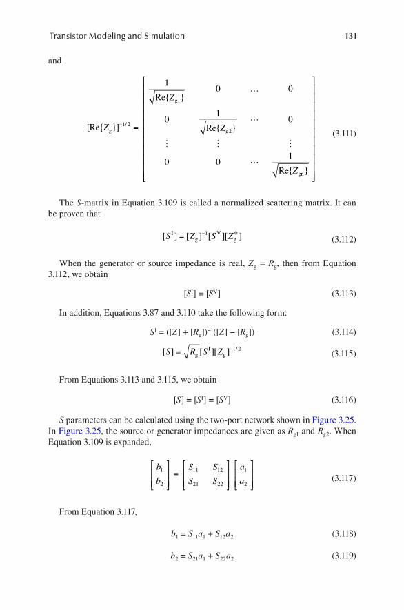
131Transistor Modeling and Simulation
and
[Re ]
Re
Re
Re
Z
Z
Z
Z
g/
g
g
g
− =1 2
1
2
10 0
01
0
0 01
…
nn
(3.111)
The S-matrix in Equation 3.109 is called a normalized scattering matrix. It can be proven that
[ ] [ ] [ ][ *]S Z S ZIg
Vg= −1
(3.112)
When the generator or source impedance is real, Zg = Rg, then from Equation 3.112, we obtain
[SI] = [SV] (3.113)
In addition, Equations 3.87 and 3.110 take the following form:
SI = ([Z] + [Rg])−1([Z] − [Rg]) (3.114)
[ ] [ ][ ]S R S Z= −g
Ig
/1 2 (3.115)
From Equations 3.113 and 3.115, we obtain
[S] = [SI] = [SV] (3.116)
S parameters can be calculated using the two-port network shown in Figure 3.25. In Figure 3.25, the source or generator impedances are given as Rg1 and Rg2. When Equation 3.109 is expanded,
b
b
S S
S S
a
a1
2
11 12
21 22
1
2
= (3.117)
From Equation 3.117,
b1 = S11a1 + S12a2 (3.118)
b2 = S21a1 + S22a2 (3.119)
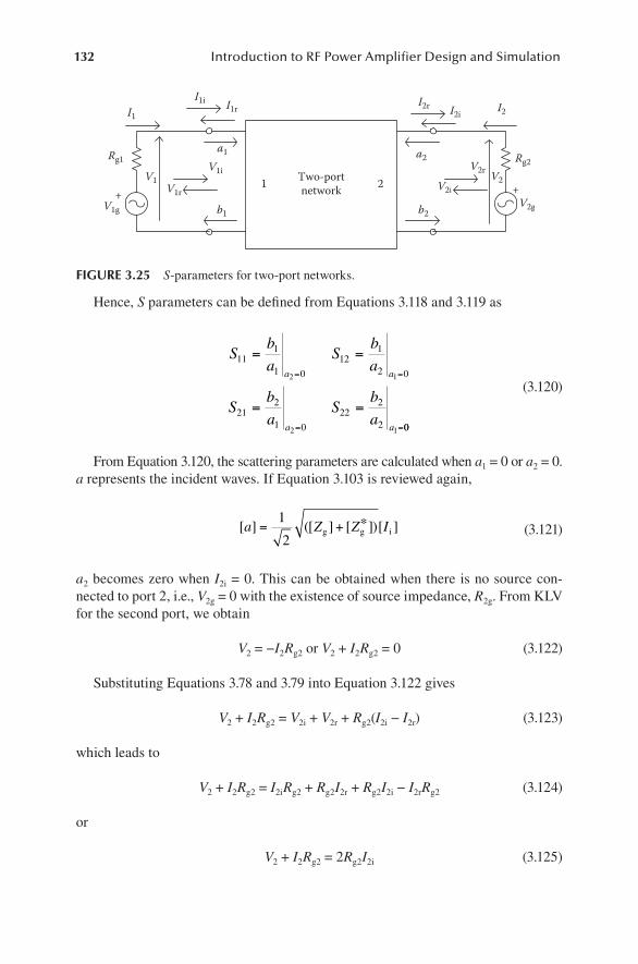
132 Introduction to RF Power Amplifier Design and Simulation
Hence, S parameters can be defined from Equations 3.118 and 3.119 as
Sb
aS
b
a
Sb
aS
b
a
a a
a a
111
1 0
121
2 0
212
1 0
222
2
2 1
2 1
= =
= =
= =
= =00
(3.120)
From Equation 3.120, the scattering parameters are calculated when a1 = 0 or a2 = 0. a represents the incident waves. If Equation 3.103 is reviewed again,
[ ] ([ ] [ *])[ ]a Z Z I= +1
2g g i (3.121)
a2 becomes zero when I2i = 0. This can be obtained when there is no source con-nected to port 2, i.e., V2g = 0 with the existence of source impedance, R2g. From KLV for the second port, we obtain
V2 = −I2Rg2 or V2 + I2Rg2 = 0 (3.122)
Substituting Equations 3.78 and 3.79 into Equation 3.122 gives
V2 + I2Rg2 = V2i + V2r + Rg2(I2i − I2r) (3.123)
which leads to
V2 + I2Rg2 = I2iRg2 + Rg2I2r + Rg2I2i − I2rRg2 (3.124)
or
V2 + I2Rg2 = 2Rg2I2i (3.125)
1 2
a1 a2
b1 b2
Two-portnetwork
V1g
Rg1
V2g
Rg2
+V1
I1
I1i I1r
V1i
V1r
I2iI2r I2
V2r
V2i +V2
FIGURE 3.25 S-parameters for two-port networks.
133Transistor Modeling and Simulation
From Equation 3.121, when Zg = Rg,
[ ] [ ]a R I= g i (3.126)
Substituting Equation 3.124 into Equation 3.125 gives
V I R R a2 2 2 2 22+ =g g (3.127)
Then,
aV I R
R2
2 2 2
22=
+ g
g
(3.128)
It is then proven that when Equation 3.122 is substituted into Equation 3.128, a2 = 0 as expected. This also requires Ii = 0 from Equation 3.127. Then, this shows that there is no reflected current, which is the incident current, I2i, at port 2 due to the source generator incident wave from port 1.
A similar analysis can be done at port 1 when a1 = 0. The same steps can be fol-lowed, and it can be shown that
aV I R
R1
1 1 1
12=
+ g
g
(3.129)
Reflected waves b1 and b2 can be analyzed the same way using the analysis just presented for the incident waves a1 and a2. When there is no source voltage con-nected at port 1, a1 = 0 in the existence of source voltage Rg1, we can write
V1 = −I1Rg1 or V1 + I1Rg1 = 0 (3.130)
In terms of the reflected and incident voltage and current, we get
V1 − I1Rg1 = V1i + V1r − Rg1(I1i − I1r) (3.131)
which leads to
V1 − I1Rg1 = I1iRg1 + I1r Rg1 − I1iRg1 + I1r Rg1 (3.132)
or
V1 − I1Rg1 = 2Rg1I1r (3.133)
134 Introduction to RF Power Amplifier Design and Simulation
From Equation 3.104, when Zg = Rg,
[ ] [ ]b R I= g r (3.134)
Hence, Equation 3.133 can be written as
V I R R b1 1 1 1 12− =g g (3.135)
Then,
bV I R
R1
1 1 1
12=
− g
g
(3.136)
It can also be shown that when a2 = 0,
bV I R
R2
2 2 2
22=
− g
g
(3.137)
The incident and reflected parameters a and b for the N-port network can be written using the results given in Equations 3.128, 3.129, 3.136, and 3.137 for real generator impedance, Rg, as
[ ] [ ] ([ ] [ ][ ])a R V R I= +−12
1 2g
/g (3.138)
[ ] [ ] ([ ] [ ][ ])b R V R I= −−12
1 2g
/g (3.139)
For an arbitrary impedance, Equations 3.138 and 3.139 can be written as
[ ] [Re ] ([ ] [ ][ ])a Z V Z I= +−12
1 2g
/g (3.140)
[ ] [Re ] ([ ] [ *][ ])b Z V Z I= −−12
1 2g
/g (3.141)
Now, since the conditions when a1 and a2 are zero were derived, the equations given by Equation 3.120 can be expanded. When a2 = 0, S11 and S21 can be calculated. From Equations 3.124, 3.126, 3.129, and 3.136, S11 can be expressed as
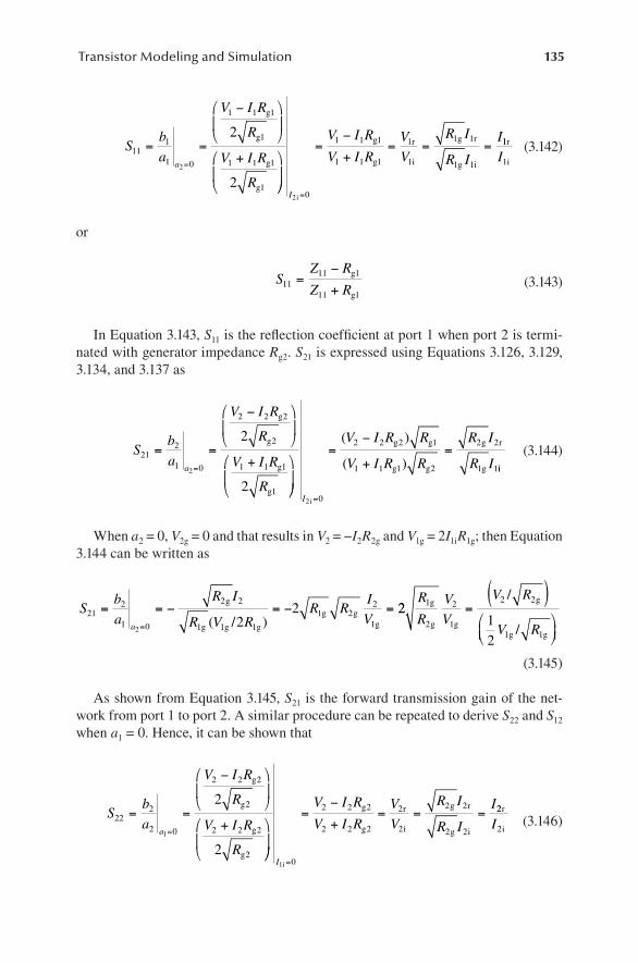
135Transistor Modeling and Simulation
Sb
a
V I R
R
V I R
R
a
111
1 0
1 1 1
1
1 1 1
1
2
2
2
= =
−
+
=
g
g
g
g
=−
+= = =
=I
V I R
V I R
V
V
R I
R I
I
2 0
1 1 1
1 1 1
1
1
1 1
1 1
i
g
g
r
i
g r
g i
11
1
r
iI (3.142)
or
SZ R
Z R1111 1
11 1
=−
+g
g (3.143)
In Equation 3.143, S11 is the reflection coefficient at port 1 when port 2 is termi-nated with generator impedance Rg2. S21 is expressed using Equations 3.126, 3.129, 3.134, and 3.137 as
Sb
a
V I R
R
V I R
R
a
212
1 0
2 2 2
2
1 1 1
1
2
2
2
= =
−
+
=
g
g
g
g
=−
+=
=I
V I R R
V I R R
R I
R I
2 0
2 2 2 1
1 1 1 2
2 2
1 1
i
g g
g g
g r
g
( )
( ) ii (3.144)
When a2 = 0, V2g = 0 and that results in V2 = −I2R2g and V1g = 2I1iR1g; then Equation 3.144 can be written as
Sb
a
R I
R V RR R
I
Va
212
1 0
2 2
1 1 1
1 22
12
22= = − = − =
=
g
g g g
g gg/( )
2212
1
2
2
1
2 2
1 1
R
R
V
V
V R
V R
g
g g
g
g g
/
/
=( )
(3.145)
As shown from Equation 3.145, S21 is the forward transmission gain of the net-work from port 1 to port 2. A similar procedure can be repeated to derive S22 and S12 when a1 = 0. Hence, it can be shown that
Sb
a
V I R
R
V I R
R
a
222
2 0
2 2 2
2
2 2 2
2
1
2
2
= =
−
+
=
g
g
g
g
=−
+= = =
=I
V I R
V I R
V
V
R I
R I
I
1 0
2 2 2
2 2 2
2
2
2 2
2 2
i
g
g
r
i
g r
g i
22
2
r
iI (3.146)
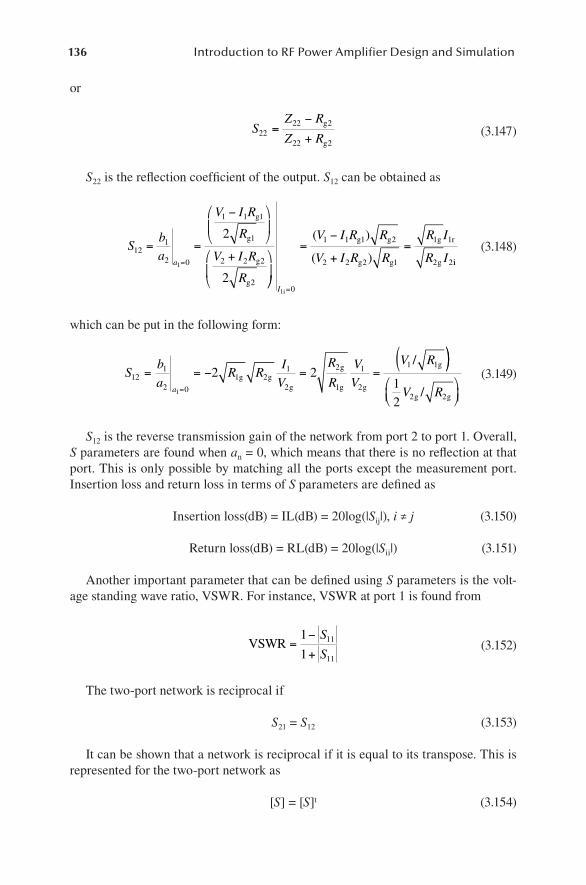
136 Introduction to RF Power Amplifier Design and Simulation
or
SZ R
Z R2222 2
22 2
=−
+g
g (3.147)
S22 is the reflection coefficient of the output. S12 can be obtained as
Sba
V I R
R
V I R
Ra
121
2 0
1 1 1
1
2 2 2
2
1
2
2
= =
−
+
=
g
g
g
g
=−
+=
=I
V I R R
V I R R
R I
R I
1 0
1 1 1 2
2 2 2 1
1 1
2 2
i
g g
g g
g r
g
( )
( ) ii
(3.148)
which can be put in the following form:
Sb
aR R
I
V
R
R
V
V
V R
a
121
2 0
1 21
2
2
1
1
2
1 1
1
2 2= = − = =(
=
g gg
g
g g
g/ ))
12 2 2V Rg g/
(3.149)
S12 is the reverse transmission gain of the network from port 2 to port 1. Overall, S parameters are found when an = 0, which means that there is no reflection at that port. This is only possible by matching all the ports except the measurement port. Insertion loss and return loss in terms of S parameters are defined as
Insertion loss(dB) = IL(dB) = 20log(|Sij|), i ≠ j (3.150)
Return loss(dB) = RL(dB) = 20log(|Sii|) (3.151)
Another important parameter that can be defined using S parameters is the volt-age standing wave ratio, VSWR. For instance, VSWR at port 1 is found from
VSWR =−
+
1
111
11
S
S (3.152)
The two-port network is reciprocal if
S21 = S12 (3.153)
It can be shown that a network is reciprocal if it is equal to its transpose. This is represented for the two-port network as
[S] = [S]t (3.154)
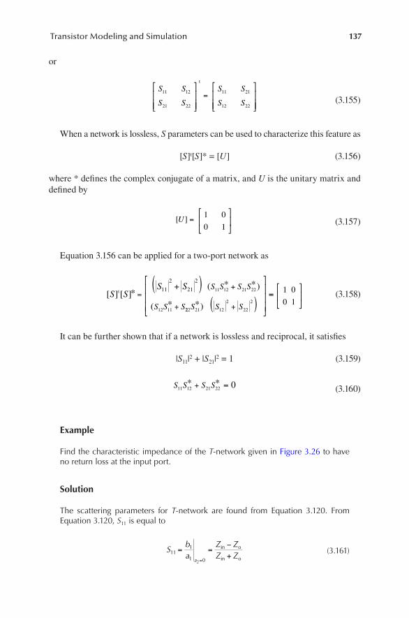
137Transistor Modeling and Simulation
or
S S
S S
S S
S S
11 12
21 22
11 21
12 22
=
t
(3.155)
When a network is lossless, S parameters can be used to characterize this feature as
[S]t[S]* = [U] (3.156)
where * defines the complex conjugate of a matrix, and U is the unitary matrix and defined by
[ ]U = 1 0
0 1 (3.157)
Equation 3.156 can be applied for a two-port network as
[ ] [ ]( * *)
( *S S
S S S S S S
S S S
t * =+
+
+( )11
2
21
2
11 12 21 22
12 11 222 21 12
2
22
2
1 0
0 1S S S*) +( )
= (3.158)
It can be further shown that if a network is lossless and reciprocal, it satisfies
|S11|2 + |S21|2 = 1 (3.159)
S S S S11 12 21 22 0* *+ = (3.160)
Example
Find the characteristic impedance of the T-network given in Figure 3.26 to have no return loss at the input port.
Solution
The scattering parameters for T-network are found from Equation 3.120. From Equation 3.120, S11 is equal to
Sba
Z ZZ Z
a
111
1 02
= =−+
=
in o
in o (3.161)
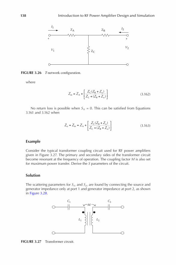
138 Introduction to RF Power Amplifier Design and Simulation
where
Z ZZ Z ZZ Z Zin A
C B o
C B o
= ++
+ +( )( ) (3.162)
No return loss is possible when S11 = 0. This can be satisfied from Equations 3.161 and 3.162 when
Z Z ZZ Z ZZ Z Zo in A
C B o
C B o
= = ++
+ +( )( ) (3.163)
Example
Consider the typical transformer coupling circuit used for RF power amplifiers given in Figure 3.27. The primary and secondary sides of the transformer circuit become resonant at the frequency of operation. The coupling factor M is also set for maximum power transfer. Derive the S parameters of the circuit.
Solution
The scattering parameters for S11 and S21 are found by connecting the source and generator impedance only at port 1 and generator impedance at port 2, as shown in Figure 3.28.
ZB
ZC
ZAI1
V1
+ +
V2
I2
FIGURE 3.26 T-network configuration.
MC2C1
L2L1
FIGURE 3.27 Transformer circuit.
139Transistor Modeling and Simulation
Application of KVL on the left and right sides of the circuit gives
V1g − I1Rg1 + jI1XC1 − jI1XL1 − jωI2M = 0 (3.164)
I2Rg2 − jI2XC2 + jI2XL2 + jωI1M = 0 (3.165)
From Equations 3.164 and 3.165, we obtain
V I R jX jXM
R jX jXg g C Lg C L
1 1 1 1 1
2
2 2 2
= − + +− +
ω (3.166)
ω2
2 2 2
MR jX jXg C L− + represented the secondary impedance referred to the primary
side. It is communicated in the problem that the circuit is at resonance with the operational frequency. Then, Equation 3.166 is simplified to
V I RM
Rg gg
1 1 1
2
2
= +
ω (3.167)
From Equation 3.167, it is seen that the maximum power transfer occurs when
RM
Rgg
1
2
2
=ω
(3.168)
Hence, the coupling factor, M, is found from Equation 3.168 as
M R R= ω g g1 2 (3.169)
As a result of Equations 3.168 and 3.169, Z11 is equal to
Z11 = Rg1 (3.170)
MC1 C2
L1 L2Vg1
Rg1V1
+ +
V2 Rg2
Z11
I1 I2
FIGURE 3.28 Transformer coupling circuit for S11 and S21.
140 Introduction to RF Power Amplifier Design and Simulation
From Equation 3.143, S11 is found as
S11 = 0 (3.171)
From Equation 3.145,
S R RIV21 1 22
1
2= − g gg
(3.172)
When Equation 3.169 is substituted into Equations 3.164 and 3.165, they are simplified to
V I R jI R R1 1 1 2 1 2 0g g g g− − = (3.173)
I R jI R R2 2 1 1 2 0g g g+ = (3.174)
Solving Equations 3.173 and 3.174 for the ratio of (I2/V1g) gives
IV
j
R R2
1 1 22g g g
=−
(3.175)
Substitution of Equation 3.175 into Equation 3.172 gives S21 as
S R Rj
R R21 1 2
1 2
22
= −−
g g
g g (3.176)
Then,
S21 = j = 1 ∠90° (3.177)
The scattering parameters for S22 and S12 are found by connecting the source and generator impedance only at port 2 and the generator impedance at port 1, as shown in Figure 3.29.
We can apply KVL for both sides of the circuit with Equation 3.169 and obtain
I R jI R R1 1 2 1 2 0g g g+ = (3.178)
V I R jI R Rg g g g2 2 2 1 1 2 0− − = (3.179)
Solving Equations 3.178 and 3.179 for Vg2 gives
Vg2 = I2(Rg1 + Rg2) (3.180)
141Transistor Modeling and Simulation
Since from Equations 3.168 and 3.169,
RMRg2
2
1
=ω
(3.181)
Then,
Z22 = Rg2 (3.182)
Substitution of Equation 3.182 into Equation 3.147 leads to
S22 = 0 (3.183)
S12 is calculated by finding the ratio of (I1/Vg2) from Equations 3.178 and 3.179 as
IV
j
R R1
2 1 22g g g
=−
(3.184)
From Equation 3.149,
S R RIV
R Rj
R R12 1 2
1
21 2
1 2
2 22
= − = −−
g g
gg g
g g (3.185)
Hence, S12 is equal to
S12 = j = 1 ∠90° (3.186)
Then, the S-matrix for a coupling transformer can be written as
Sj
j=
0
0 (3.187)
MC1 C2
+ +
V2L2L1V1
Rg2
Vg2Z22
I1 I2
Rg1
FIGURE 3.29 Transformer coupling circuit for S22 and S12.
142 Introduction to RF Power Amplifier Design and Simulation
TABLE 3.2ABCD and S Parameters of Basic Network Configurations
Z
Zz =Zo
Yy =Yo
Y
N1 : N2
ℓ
Zo, γ
Zo sinh (γℓ)
sinh (γℓ)Zo
γ = α + jβ
A
B
C
D
1
Z
0
1
1
0
Y
1
A
B
C
D
n = N1/N2
n = N1/N2
0
0
1N1
N2n
=
cosh(γℓ)
cosh(γℓ)
S11
S12
S21
S22
S11
S12
S21
S22
zz + 2
2z + 2
2y + 2
2z + 2
2y + 2
zz + 2
–yy + 2
–yy + 2 n2 + 1
n2 + 1
n2 + 1
n2 – 1
n2 – 1–n2 + 1
2n
2n
0
0
e–γℓ
e–γℓ
143Transistor Modeling and Simulation
or
S = ∠ °∠ °
0 1 901 90 0 (3.188)
The ABCD and S parameters for some of the basic RF components given in the following are shown in Table 3.2.
3.5 MEASUREMENT OF S PARAMETERS
In this section, the measurement of scattering parameters for two-port and three-port networks will be discussed. In addition, the design of test fixture to measure scatter-ing parameters will also be given.
3.5.1 measurement of S parameters for a two-port network
Two-port scattering parameters can be measured by expressing the incident and reflected waves in terms of circuit parameters. From Equations 3.118 and 3.119,
b1 = S11a1 + S12a2 (3.189)
b2 = S21a1 + S22a2 (3.190)
It was given by Equations 3.80, 3.81, 3.126, and 3.134 that
[ ] [ *][ ]V Z Ii g i= (3.191)
[Vr] = [Zg][Ir] (3.192)
[ ] [ ]a R I= g i (3.193)
[ ] [ ]b R I= g r (3.194)
Then, when there are real generator impedances, the following equations can be written:
Vi1 = Rg1Ii1 (3.195)
Vr1 = Rg1Ir1 (3.196)
Vi2 = Rg2Ii2 (3.197)
Vr2 = Rg2Ir2 (3.198)
144 Introduction to RF Power Amplifier Design and Simulation
and
a R I1 1 1= g i (3.199)
b R I1 1 1= g r (3.200)
a R I2 2 2= g i (3.201)
b R I2 2 2= g r (3.202)
When Equations 3.199 through 3.202 are substituted into Equations 3.189 and 3.190, we obtain
R I S R I S R Ig r g i g i1 1 11 1 1 12 2 2= + (3.203)
R I S R I S R Ig r g i g i2 2 21 2 1 22 2 2= + (3.204)
When the generator impedances at ports 1 and 2 are equal, i.e., Rg1 = Rg2 = R, then Equations 3.203 and 3.204 simplify to
Ir1 = S11Ii1 + S12Ii2 (3.205)
Ir2 = S21Ii1 + S22Ii2 (3.206)
Similarly,
Vr1 = S11Vi1 + S12Vi2 (3.207)
Vr2 = S21Vi1 + S22Vi2 (3.208)
Hence, from Equations 3.207 and 3.208, the scattering parameters can be mea-sured as
SV
VS
V
V
SV
VS
V V
V
111
1 0
121
2 0
212
1 0
2
2 1
2
= =
=
= =
=
r
i
r
i
r
i
i i
i
222
2 01
==
V
VV
r
ii
(3.209)
145Transistor Modeling and Simulation
As seen from Equation 3.209, the measurement of the incident and reflected volt-ages at each port while the other port is terminated by a matched port will give the scattering parameters in Equation 3.209. The incident and reflected voltage waves can be simply measured by directional couplers in practical applications.
3.5.2 measurement of S parameters for a tHree-port network
The following results are obtained by applying the same analysis for a three-port network. The incident and reflected voltage and current in terms of scattering param-eters for a three-port network are obtained as
Ir1 = S11Ii1 + S12Ii2 + S13Ii3 (3.210)
Ir2 = S21Ii1 + S22Ii2 + S23Ii3 (3.211)
Ir3 = S31Ii1 + S32Ii2 + S33Ii3 (3.212)
Similarly,
Vr1 = S11Vi1 + S12Vi2 + S13Vi3 (3.213)
Vr2 = S21Vi1 + S22Vi2 + S23Vi3 (3.214)
Vr3 = S31Vi1 + S32Vi2 + S33Vi3 (3.215)
Hence, the scattering parameters from Equations 3.210 through 3.215 are found as
SV
VS
V
V
SV
V V V V
111
1 0 0
121
2 0 0
31
2 3 1 3
= =
=
= = = =
r
i
r
ii i i i, ,
rr
i
r
ii i i i
3
1 0 0
333
3 0 02 3 1 3V
SV
VV V V V= = = =
=, ,
(3.216)
The complete conversion chart between S parameters and two-port parameters is given in Table 3.3.
146In
trod
uctio
n to
RF Po
wer A
mp
lifier D
esign an
d Sim
ulatio
n
TABLE 3.3Conversion Chart between S Parameters and Two-Port Parameters
S Z Y ABCD
S11 S11( )( )Z Z Z Z Z Z
Z11 0 22 0 12 21− + −
∆
( )( )Y Y Y Y Y Y
Y0 11 0 22 12 21− + +
∆
A B Z CZ D
A B Z CZ D
+ − −
+ + +
/
/0 0
0 0
S12 S122 12 0Z Z
Z∆
−2 12 0Y Y
Y∆
2
0 0
( )AD BC
A B Z CZ D
−+ + +/
S21 S212 21 0Z Z
Z∆
−2 21 0Y Y
Y∆
2
0 0A B Z CZ D+ + +/
S22 S22( )( )Z Z Z Z Z Z
Z11 0 22 0 12 21+ − −
∆
( )( )Y Y Y Y Y Y
Y0 11 0 22 12 21+ − +
∆
− + − +
+ + +
A B Z CZ D
A B Z CZ D
/
/0 0
0 0
Z11 ZS S S S
S S S S011 22 12 21
11 22 12 21
1 1
1 1
( )( )
( )( )
+ − +
− − −Z11
Y
Y22 A
C
Z12 ZS
S S S S012
11 22 12 21
2
1 1( )( )− − −Z12
−Y
Y12 AD BC
C
−
Z21 ZS
S S S S021
11 22 12 21
2
1 1( )( )− − −Z21
−Y
Y21 1
C
Z22 ZS S S S
S S S S011 22 12 21
11 22 12 21
1 1
1 1
( )( )
( )( )
− + +
− − −Z22
Y
Y11 D
C
(Continued)
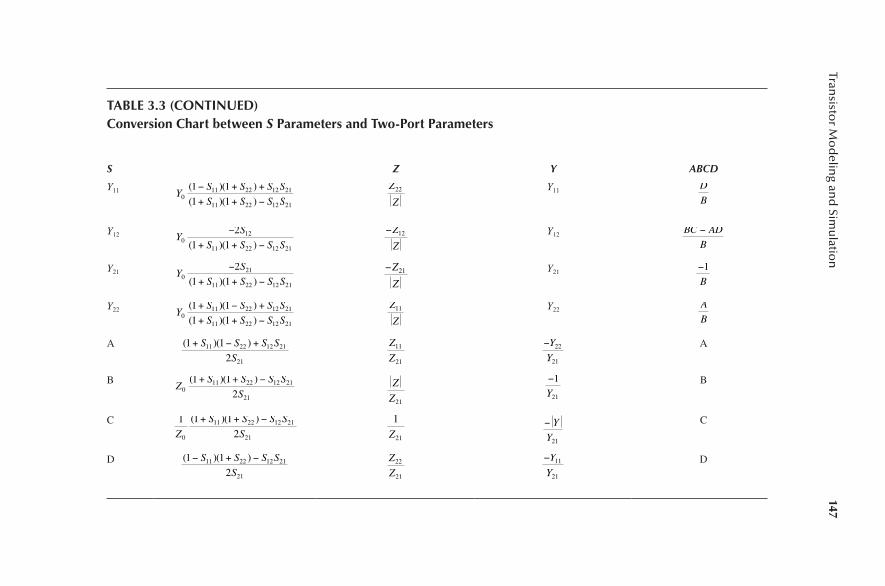
147Tran
sistor M
od
eling an
d Sim
ulatio
n
TABLE 3.3 (CONTINUED)Conversion Chart between S Parameters and Two-Port Parameters
S Z Y ABCD
Y11 YS S S S
S S S S011 22 12 21
11 22 12 21
1 1
1 1
( )( )
( )( )
− + +
+ + −
Z
Z22 Y11
D
B
Y12 YS
S S S S012
11 22 12 21
2
1 1
−
+ + −( )( )
−Z
Z12 Y12
BC AD
B
−
Y21 YS
S S S S021
11 22 12 21
2
1 1
−
+ + −( )( )−Z
Z21 Y21
−1B
Y22 YS S S S
S S S S011 22 12 21
11 22 12 21
1 1
1 1
( )( )
( )( )
+ − +
+ + −
Z
Z11 Y22
A
B
A ( )( )1 1
211 22 12 21
21
+ − +S S S S
S
Z
Z11
21
−Y
Y22
21
A
BZ
S S S S
S011 22 12 21
21
1 1
2
( )( )+ + − Z
Z21
−1
21YB
C 1 1 1
20
11 22 12 21
21Z
S S S S
S
( )( )+ + − 1
21Z− YY21
C
D ( )( )1 1
211 22 12 21
21
− + −S S S S
S
Z
Z22
21
−Y
Y11
21
D
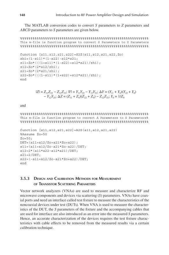
148 Introduction to RF Power Amplifier Design and Simulation
The MATLAB conversion codes to convert S parameters to Z parameters and ABCD parameters to S parameters are given below.
%%%%%%%%%%%%%%%%%%%%%%%%%%%%%%%%%%%%%%%%%%%%%%%%%%%%%%%%%%%%%%This m-file is function program to convert S Parameters to Z Parameters%%%%%%%%%%%%%%%%%%%%%%%%%%%%%%%%%%%%%%%%%%%%%%%%%%%%%%%%%%%%%% function [z11,z12,z21,z22]=S2Z(s11,s12,s21,s22,Zo)zhi=(1-s11)*(1-s22)-s12*s21;z11=Zo*(((1+s11)*(1-s22)+s12*s21)/zhi);z12=Zo*(2*s12/zhi);z21=Zo*(2*s21/zhi);z22=Zo*(((1-s11)*(1+s22)+s12*s21)/zhi);end
|Z| = Z11Z22 − Z12Z21; |Y| = Y11Y22 − Y12Y21; ΔY = (Y11 + Y0)(Y22 + Y0) − Y12Y21; ΔZ = (Z11 + Z0)(Z22 + Z0) − Z12Z21; Y0 = 1/Z0
and
%%%%%%%%%%%%%%%%%%%%%%%%%%%%%%%%%%%%%%%%%%%%%%%%%%%%%%%%%%%%%%This m-file is function program to convert A Parameters to S Parameters%%%%%%%%%%%%%%%%%%%%%%%%%%%%%%%%%%%%%%%%%%%%%%%%%%%%%%%%%%%%%%%
function [s11,s12,s21,s22]=A2S(a11,a12,a21,a22)%Assume Zo=50Zo=50;DET=(a11+a12/Zo+a21*Zo+a22);s11=(a11+a12/Zo-a21*Zo-a22)/DET;s12=2*(a11*a22-a12*a21)/DET;s21=2/DET;s22=(-a11+a12/Zo-a21*Zo+a22)/DET;end
3.5.3 desIgn and calIbratIon metHods for measurement of transIstor scatterIng parameters
Vector network analyzers (VNAs) are used to measure and characterize RF and microwave components and devices via scattering (S) parameters. VNAs have coax-ial ports and need an interface called test fixture to measure the characteristics of the noncoaxial devices under test (DUTs). When VNA is used to measure the character-istics of the DUT, the S parameters of the fixture and the accompanying cables that are used for interface are also introduced as an error into the measured S parameters. Hence, an accurate characterization of the devices requires the test fixture charac-teristics with cable effects to be removed from the measured results via a certain calibration technique.
149Transistor Modeling and Simulation
There has been an extensive study on various calibration methods and algo-rithms in the literature for characterization of RF transistors [3–10]. The network analyzer with test fixture calibration is based on the error models, which are used for correction. Two-port error correction gives more accurate results because it accounts for all of the important sources of systematic error. Systematic errors include VNA measurement errors due to impedance mismatch and leakage terms in the test setup, isolation characteristics between the reference and test signal paths, and system frequency response. The most commonly used error model for two-port calibration with automatic network analyzer is the 12-term error model [11], though modern network analyzers also use 8- or 16-term error models [12]. The 12-term error model requires measurement of a complete S parameter set of the two-port device. It has two six-term error models: one for the forward measure-ment direction and one for the reverse measurement direction. The error terms that are due to fixturing effects can be removed by modeling, de-embedding, or direct measurement of the test fixture. The advantage in using the direct measurement method is due to the fact that the precise characteristics of the fixture do not need to be known beforehand. The characteristics of the fixture are measured during the calibration process. The commonly used calibration methods based on different error models are short–open–load–thru (SOLT) and thru–reflect–line (TRL) tech-niques. The TRL method is a multiline calibration method using the zero-length through, reflection (short or open), and line standards and was first introduced by Engen and Hoer [13] and then studied extensively by other researchers [14–16]. One of the disadvantages of the TRL calibration method is that the line standards can become physically too long for practical use at low frequencies. The SOLT calibra-tion method is attractive for RF fixtures due to simpler and less-expensive fixtures and standards, which gives more accuracy at lower frequencies in comparison to the TRL method [17–20].
Typical network analyzer measurement setup for direct measurement using two-port calibration to characterize active devices is illustrated in Figure 3.30.
The effects of the test fixture including loss, length, and mismatch from the measurement can be removed if in-fixture calibration standards are available. Full two-port calibration with the conventional SOLT method based on the 12-term error model can be used to remove the effects of fixture in the measurement. Figure 3.31 illustrates the representation of the 12-term error model using forward and reverse models with a signal flow graph. There are six error terms in each model, which must be solved to accurately measure the DUT. The SOLT calibra-tion method allows the error terms to be solved accurately through the measure-ment of a set of known calibration standards. Hence, when the SOLT method is used, the calibration standards must be well known in terms of their scattering parameters in order to achieve the accurate DUT measurements. This requires accurate modeling and characterization of calibration standards, which will be detailed in Section 3.5.3.1.
The DUT in Figure 3.31 is considered to be a two-port device. When the DUT is a bipolar junction transistor (BJT), it can be treated as a two-port device if it is oper-ated in a common emitter configuration.
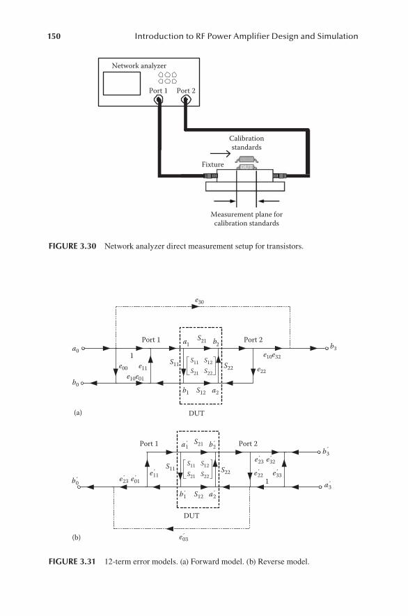
150 Introduction to RF Power Amplifier Design and Simulation
Network analyzer
Port 1 Port 2
Calibrationstandards
Measurement plane forcalibration standards
Fixture DUT
FIGURE 3.30 Network analyzer direct measurement setup for transistors.
1
21S
DUT
e30
a0
e00 e11e10e01
e10e32
e22S11 S22
b1 S12 a2
b3
b0
1a 2bPort 1 Port 2
DUT
b3a1 b2
a3a2b1
e11 e22
e03
e33
e23 e32
e23 e01
Port 1 Port 2
1
(a)
(b)
b0
S22S11
S21
S12
S11S21
S12S22
S11S21
S12S22
FIGURE 3.31 12-term error models. (a) Forward model. (b) Reverse model.
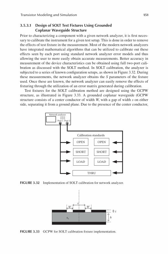
151Transistor Modeling and Simulation
3.5.3.1 Design of SOLT Test Fixtures Using Grounded Coplanar Waveguide Structure
Prior to characterizing a component with a given network analyzer, it is first neces-sary to calibrate the instrument for a given test setup. This is done in order to remove the effects of test fixture in the measurement. Most of the modern network analyzers have integrated mathematical algorithms that can be utilized to calibrate out these effects seen by each port using standard network analyzer error models and thus allowing the user to more easily obtain accurate measurements. Better accuracy in measurement of the device characteristics can be obtained using full two-port cali-bration as discussed with the SOLT method. In SOLT calibration, the analyzer is subjected to a series of known configuration setups, as shown in Figure 3.32. During these measurements, the network analyzer obtains the S parameters of the fixture used. Once these are known, the network analyzer can easily remove the effects of fixturing through the utilization of an error matrix generated during calibration.
Test fixtures for the SOLT calibration method are designed using the GCPW structure, as illustrated in Figure 3.33. A grounded coplanar waveguide (GCPW structure consists of a center conductor of width W, with a gap of width s on either side, separating it from a ground plane. Due to the presence of the center conductor,
Calibration standards
Network analyzer
Port 1 Port 2
OPEN
SHORT
LOAD
THRU
OPEN
SHORT
LOAD
FIGURE 3.32 Implementation of SOLT calibration for network analyzer.
W Ws
h
t
εr
FIGURE 3.33 GCPW for SOLT calibration fixture implementation.
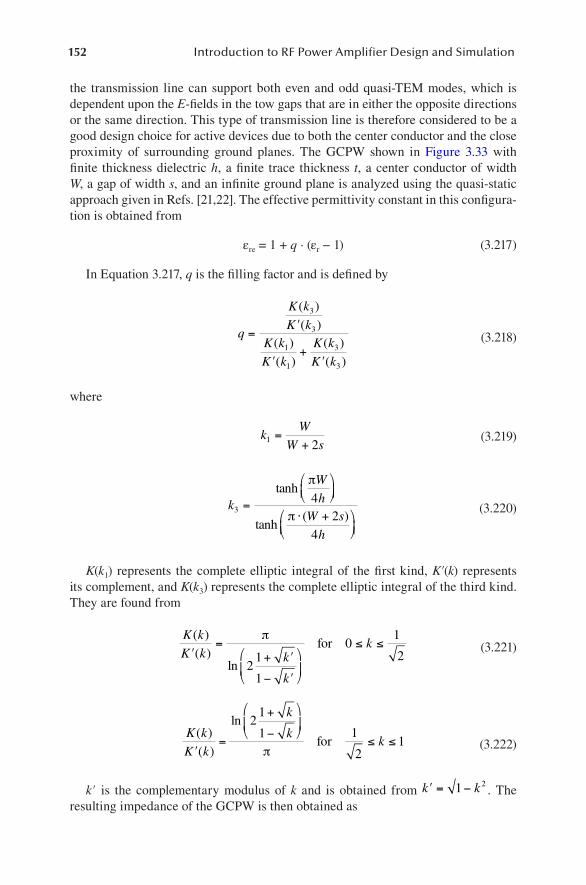
152 Introduction to RF Power Amplifier Design and Simulation
the transmission line can support both even and odd quasi-TEM modes, which is dependent upon the E-fields in the tow gaps that are in either the opposite directions or the same direction. This type of transmission line is therefore considered to be a good design choice for active devices due to both the center conductor and the close proximity of surrounding ground planes. The GCPW shown in Figure 3.33 with finite thickness dielectric h, a finite trace thickness t, a center conductor of width W, a gap of width s, and an infinite ground plane is analyzed using the quasi-static approach given in Refs. [21,22]. The effective permittivity constant in this configura-tion is obtained from
εre = 1 + q ∙ (εr − 1) (3.217)
In Equation 3.217, q is the filling factor and is defined by
q
K k
K kK k
K k
K k
K k
=′
′+
′
( )( )
( )( )
( )( )
3
3
1
1
3
3
(3.218)
where
kW
W s1 2=
+ (3.219)
k
W
hW s
h
34
24
=
⋅ +
tanh
tanh( )
π
π (3.220)
K(k1) represents the complete elliptic integral of the first kind, K′(k) represents its complement, and K(k3) represents the complete elliptic integral of the third kind. They are found from
K k
K k k
k
k( )( )
ln′
=+ ′
− ′
≤ ≤π
21
1
01
2for (3.221)
K k
K k
k
kk
( )( )
ln
′=
+
−
≤ ≤
21
1 1
21
πfor (3.222)
k′ is the complementary modulus of k and is obtained from ′ = −k k1 2. The
resulting impedance of the GCPW is then obtained as
153Transistor Modeling and Simulation
ZK kK k
K kK k
= ⋅
′+
′
60 1
1
1
3
3
π
εre ( )( )
( )( )
(3.223)
The effects of the trace thickness are included using a first-order correction factor on the conductor width and gap as
se = s − Δ (3.224)
We = W + Δ (3.225)
The correction factor, Δ, is given by
∆ = ⋅ +
1 25
14.
lnt W
tππ
(3.226)
The trace thickness can be included in the impedance calculation given by Equation 3.223 using effective modulus ke, which is given by
kW
W sk k
see
e e
=+
≈ + −( ) ⋅2
121 1
2 ∆ (3.227)
and effective modulus εret given by
ε εε
ret
re
re
= −⋅ − ⋅
′+ ⋅
0 7 1
0 71
1
. ( )
( )( )
.
ts
K kK k
ts
(3.228)
In Equation 3.228, t represents the trace thickness, and s represents the noncor-rected gap of the coplanar waveguide (CPW). Substituting the modulus values of ke and εre
t back into the impedance formula gives the final impedance of the GCPW as
ZK kK k
K kK k
= ⋅
′+
′
60 1
3
3
π
εret e
e
( )( )
( )( )
(3.229)
Since the impedance of GCPW is obtained and given by Equation 3.229, the next design parameter to consider is the physical length of the transmission line. The physical length of the transmission line is obtained from
le
=⋅l λ
360 (3.230)
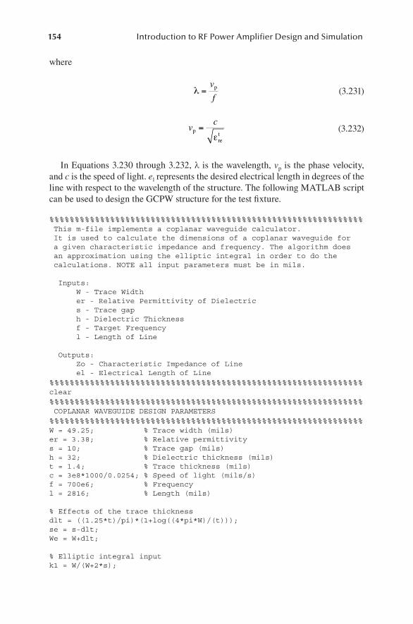
154 Introduction to RF Power Amplifier Design and Simulation
where
λ =v
fp (3.231)
vc
p
ret
=ε
(3.232)
In Equations 3.230 through 3.232, λ is the wavelength, vp is the phase velocity, and c is the speed of light. el represents the desired electrical length in degrees of the line with respect to the wavelength of the structure. The following MATLAB script can be used to design the GCPW structure for the test fixture.
%%%%%%%%%%%%%%%%%%%%%%%%%%%%%%%%%%%%%%%%%%%%%%%%%%%%%%%%%%%%%% This m-file implements a coplanar waveguide calculator. It is used to calculate the dimensions of a coplanar waveguide for a given characteristic impedance and frequency. The algorithm does an approximation using the elliptic integral in order to do the calculations. NOTE all input parameters must be in mils.
Inputs: W - Trace Width er - Relative Permittivity of Dielectric s - Trace gap h - Dielectric Thickness f - Target Frequency l - Length of Line Outputs: Zo - Characteristic Impedance of Line el - Electrical Length of Line %%%%%%%%%%%%%%%%%%%%%%%%%%%%%%%%%%%%%%%%%%%%%%%%%%%%%%%%%%%%%%clear%%%%%%%%%%%%%%%%%%%%%%%%%%%%%%%%%%%%%%%%%%%%%%%%%%%%%%%%%%%%%% COPLANAR WAVEGUIDE DESIGN PARAMETERS %%%%%%%%%%%%%%%%%%%%%%%%%%%%%%%%%%%%%%%%%%%%%%%%%%%%%%%%%%%%%%W = 49.25; % Trace width (mils)er = 3.38; % Relative permittivitys = 10; % Trace gap (mils)h = 32; % Dielectric thickness (mils)t = 1.4; % Trace thickness (mils)c = 3e8*1000/0.0254; % Speed of light (mils/s)f = 700e6; % Frequencyl = 2816; % Length (mils) % Effects of the trace thickness dlt = ((1.25*t)/pi)*(1+log((4*pi*W)/(t)));se = s-dlt;We = W+dlt; % Elliptic integral input k1 = W/(W+2*s);

155Transistor Modeling and Simulation
% Elliptic integral input k3num = tanh((pi*W)/(4*h));k3den = tanh((pi*(W+2*s))/(4*h));k3 = k3num/k3den;
% Elliptic integral input ke = We/(We+2*se);ke = k1+(1-k1^2)*(dlt/(2*s));%%%%%%%%%%%%%%%%%%%%%%%%%%%%%%%%%%%%%%%%%%%%%%%%%%%%%%%%%%%%%% ELLIPTIC INTEGRAL APPROXIMATIONS %%%%%%%%%%%%%%%%%%%%%%%%%%%%%%%%%%%%%%%%%%%%%%%%%%%%%%%%%%%%%%
k1u=sqrt(1-k1^2);if k1>=0 & k1<=(1/sqrt(2)) kk1=pi/log((2*(1+sqrt(k1u))/(1-sqrt(k1u))));elseif k1>(1/sqrt(2)) & k1<=1 kk1=log((2*(1+sqrt(k1)))/(1-sqrt(k1)))/pi;end;k3u=sqrt(1-k3^2);if k3>=0 & k3<=(1/sqrt(2)) kk3=pi/log((2*(1+sqrt(k3u))/(1-sqrt(k3u))));elseif k3>(1/sqrt(2)) & k3<=1 kk3=log((2*(1+sqrt(k3)))/(1-sqrt(k3)))/pi;end;
keu=sqrt(1-ke^2);if ke>=0 & ke<=(1/sqrt(2)) kke=pi/log((2*(1+sqrt(keu))/(1-sqrt(keu))));elseif ke>(1/sqrt(2)) & ke<=1 kke=log((2*(1+sqrt(ke)))/(1-sqrt(ke)))/pi;end;
% Filling factorq = (kk3)/(kk1+kk3);
%%%%%%%%%%%%%%%%%%%%%%%%%%%%%%%%%%%%%%%%%%%%%%%%%%%%%%%%%%%%%% EFFECTIVE PERMITTIVITY%%%%%%%%%%%%%%%%%%%%%%%%%%%%%%%%%%%%%%%%%%%%%%%%%%%%%%%%%%%%%%ere3 = 1+q*(er-1);ere4 = ere3-((0.7*(ere3-1)*(t/s))/(kk1+0.7*(t/s))); %%%%%%%%%%%%%%%%%%%%%%%%%%%%%%%%%%%%%%%%%%%%%%%%%%%%%%%%%%%%%% ELECTRICAL LENGTH (degrees) %%%%%%%%%%%%%%%%%%%%%%%%%%%%%%%%%%%%%%%%%%%%%%%%%%%%%%%%%%%%%%vp = c/sqrt(ere4); % Phase velocitylambda = vp/f; % Lambdaround = floor(l/lambda)*lambda; % Nearest whole wavelengthl = l-round; % 360 degree constrainedel = (l/lambda)*(360) % Electrical length (degrees) %%%%%%%%%%%%%%%%%%%%%%%%%%%%%%%%%%%%%%%%%%%%%%%%%%%%%%%%%%%%%% IMPEDANCE OF THE LINE%%%%%%%%%%%%%%%%%%%%%%%%%%%%%%%%%%%%%%%%%%%%%%%%%%%%%%%%%%%%%%Zo = ((60*pi)/(sqrt(ere4)))*(1/(kke+kk3))
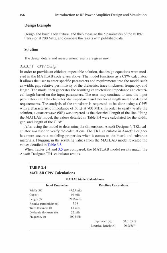
156 Introduction to RF Power Amplifier Design and Simulation
Design Example
Design and build a test fixture, and then measure the S parameters of the BFR92 transistor at 700 MHz, and compare the results with published data.
Solution
The design details and measurement results are given next.
3.5.3.1.1 CPW DesignIn order to provide an efficient, repeatable solution, the design equations were mod-eled in the MATLAB code given above. The model functions as a CPW calculator. It allows the user to enter specific parameters and requirements into the model such as width, gap, relative permittivity of the dielectric, trace thickness, frequency, and length. The model then generates the resulting characteristic impedance and electri-cal length based on the input parameters. The user may continue to tune the input parameters until the characteristic impedance and electrical length meet the defined requirements. The analysis of the transistor is requested to be done using a CPW with a characteristic impedance of 50 Ω at 700 MHz. In order to easily verify the solution, a quarter wave (90°) was targeted as the electrical length of the line. Using the MATLAB model, the values detailed in Table 3.4 were calculated for the width, gap, and length of the CPW.
After using the model to determine the dimensions, Ansoft Designer’s TRL cal-culator was used to verify the calculations. The TRL calculator in Ansoft Designer has more accurate modeling properties when it comes to the board and substrate materials. Plugging in the resulting values from the MATLAB model revealed the values detailed in Table 3.5.
When Tables 3.4 and 3.5 are compared, the MATLAB model results match the Ansoft Designer TRL calculator results.
TABLE 3.4MATLAB CPW Calculations
MATLAB Model Calculations
Input Parameters Resulting Calculations
Width (W) 49.25 mils
Gap (s) 10 mils
Length (l) 2816 mils
Relative permittivity (εr) 3.38
Trace thickness (t) 1.4 mils
Dielectric thickness (h) 32 mils
Frequency (f) 700 MHz
Impedance (Z0) 50.0105 ΩElectrical length (el) 90.0535°

157Transistor Modeling and Simulation
3.5.3.1.2 Quarter-Wave Stub DesignThe stubs were to be designed using a parallel coaxial line and attached to both the input and output ports. The stubs are “invisible” at the design frequency of 700 MHz. The target frequency chosen was 100 MHz for the quarter-wave stub design. Ansoft Designer’s coaxial line TRL calculator was used to design the quarter-wave 50 Ω coaxial stub lines at 100 MHz. From the calculator, a length of 29,507 mils is calculated for the stub.
3.5.3.1.3 SOLT Test FixturesThe SOLT test fixtures are designed repeating the method described above; they are implemented as shown in Figures 3.34 through 3.37. Rogers 4003 with relative permittivity of 3.38 is used as a dielectric substrate. The board material has substrate thickness of 0.060 in. with 1-oz. copper plating on both sides. The gap size of 10 mils is used as discussed and illustrated in Figure 3.33. In addition, several biases were
TABLE 3.5Ansoft Designer CPW Calculations
Ansoft Designer TRL Calculations
Input Parameters Resulting Calculations
Width (W) 49.25 mils
Gap (s) 10 mils
Length (l) 2816 mils
Relative permittivity (εr) 3.38
Trace thickness (t) 1.4 mils
Dielectric thickness (h) 32 mils
Frequency (f) 700 MHz
Impedance (Z0) 50.1467 ΩElectrical length (el) 90.5856°
FIGURE 3.34 “Thru” calibration test fixture—top view.
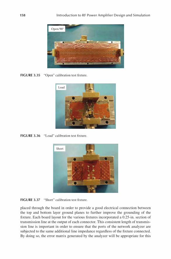
158 Introduction to RF Power Amplifier Design and Simulation
placed through the board in order to provide a good electrical connection between the top and bottom layer ground planes to further improve the grounding of the fixture. Each board layout for the various fixtures incorporated a 0.25-in. section of transmission line at the output of each connector. This consistent length of transmis-sion line is important in order to ensure that the ports of the network analyzer are subjected to the same additional line impedance regardless of the fixture connected. By doing so, the error matrix generated by the analyzer will be appropriate for this
Open/90°
FIGURE 3.35 “Open” calibration test fixture.
Load
FIGURE 3.36 “Load” calibration test fixture.
Short
FIGURE 3.37 “Short” calibration test fixture.
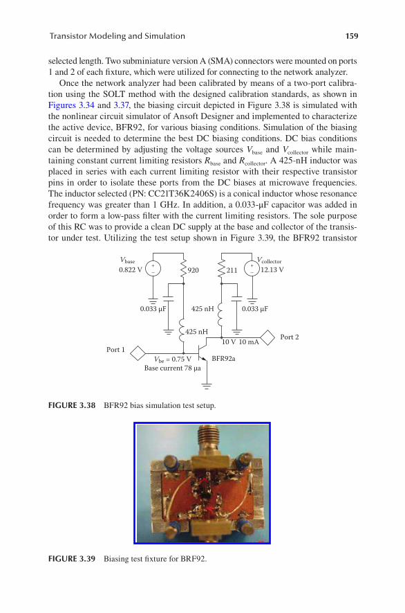
159Transistor Modeling and Simulation
selected length. Two subminiature version A (SMA) connectors were mounted on ports 1 and 2 of each fixture, which were utilized for connecting to the network analyzer.
Once the network analyzer had been calibrated by means of a two-port calibra-tion using the SOLT method with the designed calibration standards, as shown in Figures 3.34 and 3.37, the biasing circuit depicted in Figure 3.38 is simulated with the nonlinear circuit simulator of Ansoft Designer and implemented to characterize the active device, BFR92, for various biasing conditions. Simulation of the biasing circuit is needed to determine the best DC biasing conditions. DC bias conditions can be determined by adjusting the voltage sources Vbase and Vcollector while main-taining constant current limiting resistors Rbase and Rcollector. A 425-nH inductor was placed in series with each current limiting resistor with their respective transistor pins in order to isolate these ports from the DC biases at microwave frequencies. The inductor selected (PN: CC21T36K2406S) is a conical inductor whose resonance frequency was greater than 1 GHz. In addition, a 0.033-μF capacitor was added in order to form a low-pass filter with the current limiting resistors. The sole purpose of this RC was to provide a clean DC supply at the base and collector of the transis-tor under test. Utilizing the test setup shown in Figure 3.39, the BFR92 transistor
VcollectorVbase0.822 V
0.033 µF
920
425 nH 0.033 µF
12.13 V
Port 2Port 1
10 V 10 mA
BFR92aVbe = 0.75 VBase current 78 µa
+–
+–
425 nH
211
FIGURE 3.38 BFR92 bias simulation test setup.
FIGURE 3.39 Biasing test fixture for BRF92.
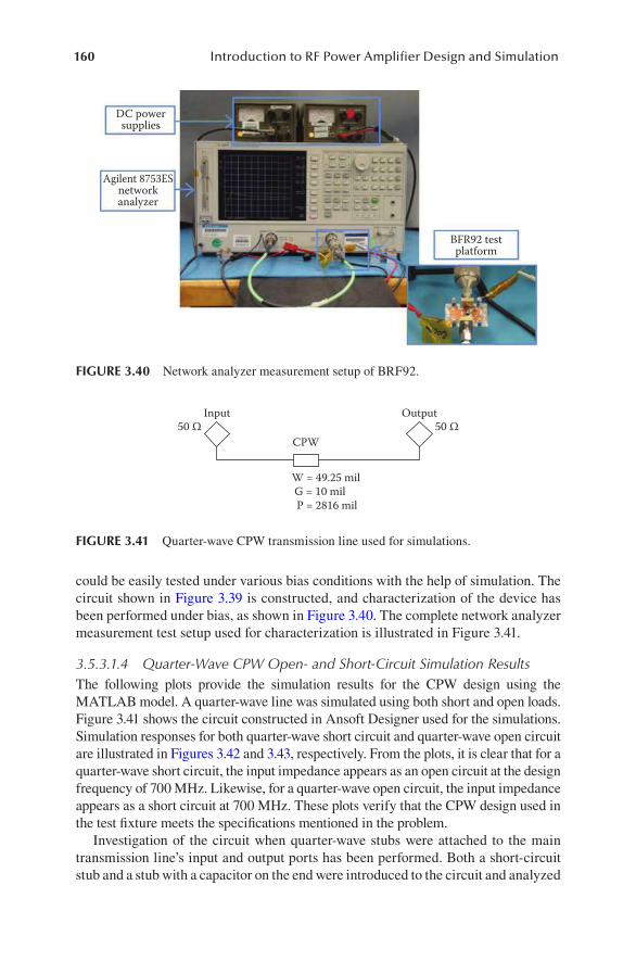
160 Introduction to RF Power Amplifier Design and Simulation
could be easily tested under various bias conditions with the help of simulation. The circuit shown in Figure 3.39 is constructed, and characterization of the device has been performed under bias, as shown in Figure 3.40. The complete network analyzer measurement test setup used for characterization is illustrated in Figure 3.41.
3.5.3.1.4 Quarter-Wave CPW Open- and Short-Circuit Simulation ResultsThe following plots provide the simulation results for the CPW design using the MATLAB model. A quarter-wave line was simulated using both short and open loads. Figure 3.41 shows the circuit constructed in Ansoft Designer used for the simulations. Simulation responses for both quarter-wave short circuit and quarter-wave open circuit are illustrated in Figures 3.42 and 3.43, respectively. From the plots, it is clear that for a quarter-wave short circuit, the input impedance appears as an open circuit at the design frequency of 700 MHz. Likewise, for a quarter-wave open circuit, the input impedance appears as a short circuit at 700 MHz. These plots verify that the CPW design used in the test fixture meets the specifications mentioned in the problem.
Investigation of the circuit when quarter-wave stubs were attached to the main transmission line’s input and output ports has been performed. Both a short- circuit stub and a stub with a capacitor on the end were introduced to the circuit and analyzed
DC powersupplies
Agilent 8753ESnetworkanalyzer
BFR92 testplatform
FIGURE 3.40 Network analyzer measurement setup of BRF92.
CPW
Input
W = 49.25 mil G = 10 mil P = 2816 mil
Output50 Ω50 Ω
FIGURE 3.41 Quarter-wave CPW transmission line used for simulations.
161Transistor Modeling and Simulation
in Ansoft Designer. Before attaching the stubs, the S parameters of the CPW trans-mission line were captured to serve as a reference when comparing the results with the stubs attached. Figure 3.44 provides the plot of the S parameters with no stubs attached. It is shown in Figure 3.35 that S11 = S22 and S12 = S21. This is consistent with what would be expected. There should be no forward (S21) or reverse gain (S12) and very little reflection at both ends (S11 and S22) due to the 50 Ω transmission line, which provides a good impedance match to the ports.
Figure 3.45 shows the circuit in Ansoft Designer used for the analysis to verify that short-circuit stub attached to the input port is “invisible” at the design frequency of 700 MHz. Ansoft Designer is also used to do the same analysis, only replacing the
10,000.00
8000.00
6000.00
4000.00
2000.00
0.000.00 0.20 0.40 0.60
F (GHz)
mag
(ZIN
)
0.80 1.00
X1 = 0.70 GHzY1 = 9048.72
FIGURE 3.42 Quarter-wave short-circuit simulation.
250.00
200.00
150.00
100.00
50.00
0.000.00 0.20 0.40 0.60
F (GHz)
mag
(ZIN
)
0.80 1.00
X1 = 0.70 GHzY1 = 0.28
FIGURE 3.43 Quarter-wave open-circuit simulation.
162 Introduction to RF Power Amplifier Design and Simulation
short end of the stub by a small capacitor, which results in an open-circuit stub at high frequencies. Simulations were run, and the S parameters were captured and plotted. Figures 3.46 and 3.47 provide the plots of the S parameters for the short- circuit and capacitor-attached cases, respectively. Note that the capacitor was removed for the short-circuit stub analysis.
From the results in Figures 3.46 and 3.47, it is clear that neither the short- nor open-circuit quarter-wave stubs had any negative effects on the circuit’s performance at the design frequency of 700 MHz. In both cases, the forward and reverse gains as well as the reflection coefficients at both ports were unaffected. Ansoft Designer
0.00
–20.00
–40.00
–60.00
–80.000.00 0.20 0.40 0.60
F (GHz)
Y1
0.80 1.00
FIGURE 3.44 S parameters of CPW transmission line without stubs attached.
Input Output50 Ω50 Ω
CPW
W = 49.25 mil G = 10 mil P = 2816 mil
Z = 50P = 29507 mil
0.001 pF
0
Coax stub(100 MHz)
FIGURE 3.45 Quarter-wave stub attached to input port.
163Transistor Modeling and Simulation
is also used to attach the same short and open stub to the output port and verify that the stub is again “invisible” at the design frequency of 700 MHz, as shown in Figure 3.48. Simulations were run, and the S parameters were captured and plotted. Figures 3.49 and 3.50 provide the plots of the S parameters for the short-circuit and capacitor-attached cases, respectively. Note that the capacitor was removed for the short-circuit stub analysis.
From the results in Figures 3.44 and 3.45, it is clear that neither the short- nor open-circuit quarter-wave stubs had any negative effects on the circuit’s performance
640.00–60.00
–40.00
–20.00
0.00
20.00
660.00
Y1dB(S21)NWA1
dB(S22)NWA1
dB(S11)NWA1
dB(S12)NWA1
Y1Y1
Y1
680.00 700.00F (MHz)
Y1
720.00 740.00 760.00
FIGURE 3.46 Quarter-wave short-circuit stub attached at input port.
640.00–100.00
–80.00
–60.00
–40.00
–20.00
0.00
20.00
660.00
Y1dB(S21)NWA1
dB(S22)NWA1
dB(S11)NWA1
dB(S12)NWA1
Y1Y1
Y1
680.00 700.00F (MHz)
Y1
720.00 740.00 760.00
FIGURE 3.47 Quarter-wave stub with capacitor attached at input port.
164 Introduction to RF Power Amplifier Design and Simulation
at the design frequency of 700 MHz. Both the forward and reverse gains were unaf-fected in both cases. However, the reflection coefficients in the short-circuit case actually provided better performance (20–30 dB) than the original circuit.
3.5.3.1.5 Measurement ResultsS parameter characterization data are obtained with the manufactured calibration set shown in Figure 3.40 and test fixtures shown in Figures 3.34 through 3.37. The BFR92 transistor was measured under the six different bias conditions detailed in Table 3.1. The measured DC gain under each biasing condition is summarized in the
Input Output50 Ω50 Ω
CPW
W = 49.25 mil G = 10 mil P = 2816 mil
Z = 50P = 29507 mil
0.001 pF
0
Coax stub(100 MHz)
Z = 50P = 29507 mil
0.001 pF
0
Coax stub(100 MHz)
FIGURE 3.48 Quarter-wave stub attached to both input and output ports.
640.00–100.00
–50.00
–75.00
–25.00
0.00
25.00
660.00
Y1dB(S21)NWA1
dB(S22)NWA1
dB(S11)NWA1
dB(S12)NWA1
Y1Y1
Y1
680.00 700.00F (MHz)
Y1
720.00 740.00 760.00
FIGURE 3.49 Quarter-wave short-circuit stub attached to both input and output ports.
165Transistor Modeling and Simulation
column titled “β” in Table 3.6. The measured S parameters were then plotted with the vendor-supplied spice model under the same biasing conditions, as well as the catalog vendor data for the given biases. These results are detailed in Figures 3.51 through 3.54 when VCE = 10[V] and Ic = 5[mA]. As detailed in the S parameter plots, the data measured using the BFR92 test fixture aligned themselves closely with both the vendor-supplied spice model and the vendor catalog data. The comparison of the measured and simulated data has also been done for all other conditions shown in Table 3.6. The agreement again was seen on all of them.
3.6 CHAIN SCATTERING PARAMETERS
When amplifier networks are cascaded, as shown in Figure 3.55, and the relation between the incident and reflected waves using scattering parameters is requested to be established, mathematically, it is more efficient to use a direct matrix multiplication
640.00–100.00
–50.00
–75.00
–25.00
0.00
25.00
660.00
Y1dB(S21)NWA1
dB(S22)NWA1
dB(S11)NWA1
dB(S12)NWA1
Y1 Y1
Y1
680.00 700.00F (MHz)
Y1
720.00 740.00 760.00
FIGURE 3.50 Quarter-wave stub with capacitor attached at both input and output ports.
TABLE 3.6DC Bias Conditions
VCE IC VBE Vbase Vcollector IB β10 V 5 mA 0.769 V 0.823 V 11.04 V 59 μa 85
10 V 10 mA 0.765 V 0.865 V 12.11 V 109 μa 91
10 V 15 mA 0.751 V 0.889 V 13.16 V 150 μa 100
5 V 5 mA 0.785 V 0.845 V 6.05 V 65 μa 77
5 V 10 mA 0.794 V 0.909 V 7.10 V 125 μa 80
5 V 15 mA 0.797 V 0.966 V 8.15 V 184 μa 82
166 Introduction to RF Power Amplifier Design and Simulation
similar to ABCD matrices. The chain scattering matrix, T, is introduced to fulfill this requirement. The chain scattering matrix, T, can be expressed in terms of incident and reflected waves as
a
b
T T
T T
b
a1
1
11 12
21 22
2
2
= (3.233)
5.002.001.000.500.200.00
5.00
–5.00
2.00
–2.00
1.00
–1.00
0.50
–0.50
0.20
–0.20
0.00
20
30
40
50
60
7080100
110
120
130
140
150
60
60
–150
–140
–130
–120
–70–110
–60
–50
–40
–30
–20
–
Simulated S11Red
Green Data sheet S11
Measured S11Blue
FIGURE 3.51 Input return loss comparison (S11); VCE = 10 V, IC = 5 mA.
5.002.001.000.500.200.00
5.00
–5.00
2.00
–2.00
1.00
–1.00
0.50
–0.50
0.20
-0.20
0.00
20
30
40
50
60
7080100
110
120
130
140
150
60
60
–150
–140
–130
–120
–70–110
–60
–50
–40
–30
–20
–
Simulated S11Red
Green Data sheet S11
Measured S11Blue
FIGURE 3.52 Output return loss comparison (S22); VCE = 10 V, IC = 5 mA.
167Transistor Modeling and Simulation
S 12 (
dB)
Simulated S11RedGreen Data sheet S11
Measured S11Blue
0.10–35.00
–32.50
–30.00
–27.50
–25.00
–22.50
–20.00
0.20 0.30 0.40 0.50 0.60F (GHz)
0.70 0.80 0.90 1.00
Red = Spice model performanceGreen = Phillips catalog dataBlue = measured BFR92 data
Curved infodB(S(Spice1, Spice2))LinearFrequencydB(S(Sparam1, Sparam2))LinearFrequencydB(S(Meas1, Meas2))LinearFrequency
FIGURE 3.53 Reverse isolation comparison (S12); VCE = 10 V, IC = 5 mA.
S 12 (
dB)
0.100.00
12.50
15.00
17.50
20.00
22.50
0.20 0.30 0.40 0.50 0.60F (GHz)
0.70 0.80 0.90 1.00
Red = Spice model performanceGreen = Phillips catalog dataBlue = measured BFR92 data
Curved infodB(S(Spice1, Spice2))LinearFrequencydB(S(Sparam1, Sparam2))LinearFrequencydB(S(Meas1, Meas2))LinearFrequency
Simulated S11RedGreen Data sheet S11
Measured S11Blue
FIGURE 3.54 Forward gain comparison (S21); VCE = 10 V, IC = 5 mA.
a1A
b1A
b1B
a1B
a2A
b2A
a2B
b2B
Port 1T A
Port 2Network A Network B
T B
FIGURE 3.55 Illustration of chain scattering matrix for cascaded networks.
168 Introduction to RF Power Amplifier Design and Simulation
Hence, the chain scattering matrices for networks A and B can be written as
a
b
T T
T T
b
a
1
1
11 12
21 22
2
2
A
A
A A
A A
A
A= (3.234)
a
b
T T
T T
b
a
1
1
11 12
21 22
2
2
B
B
B B
B B
B
B= (3.235)
It is also seen from Figure 3.55 that
a
b
b
a
2
2
1
1
A
A
B
B= (3.236)
Then, using Equation 3.236, we can turn Equation 3.235 into Equation 3.234 and obtain
a
b
T T
T T
T T1
1
11 12
21 22
11 12A
A
A A
A A
B B
=TT T
b
a21 22
2
2B B
B
B (3.237)
or
a
bT
b
a
1
1
2
2
A
A
B
B= [ ] (3.238)
where
[T] = [TA][T B] (3.239)
and
[ ]TT T
T TA
A A
A A= 11 12
21 22 (3.240)
and
[ ]TT T
T TB
B B
B B= 11 12
21 22 (3.241)
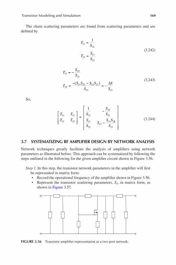
169Transistor Modeling and Simulation
The chain scattering parameters are found from scattering parameters and are defined by
TS
TS
S
1121
2111
21
1=
=
(3.242)
TS
S
TS S S S
S
S
S
1222
21
2211 22 12 21
21 21
= −
=− −
= −( ) ∆
(3.243)
So,
T T
T T
S
S
S
S
SS
S S11 12
21 22
21
22
21
11
2112
11 2
1
=
−
− 22
21S
(3.244)
3.7 SYSTEMATIZING RF AMPLIFIER DESIGN BY NETWORK ANALYSIS
Network techniques greatly facilitate the analysis of amplifiers using network parameters as illustrated before. This approach can be systematized by following the steps outlined in the following for the given amplifier circuit shown in Figure 3.56.
Step 1. In this step, the transistor network parameters in the amplifier will first be represented in matrix form:• Record the operational frequency of the amplifier shown in Figure 3.56.• Represent the transistor scattering parameters, ST, in matrix form, as
shown in Figure 3.57.
FIGURE 3.56 Transistor amplifier representation as a two-port network.
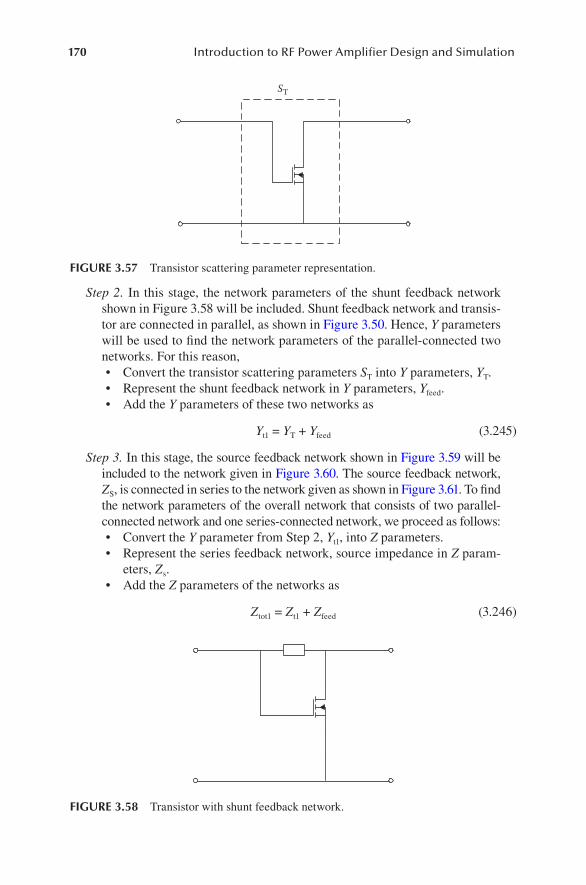
170 Introduction to RF Power Amplifier Design and Simulation
Step 2. In this stage, the network parameters of the shunt feedback network shown in Figure 3.58 will be included. Shunt feedback network and transis-tor are connected in parallel, as shown in Figure 3.50. Hence, Y parameters will be used to find the network parameters of the parallel-connected two networks. For this reason,• Convert the transistor scattering parameters ST into Y parameters, YT.• Represent the shunt feedback network in Y parameters, Yfeed.• Add the Y parameters of these two networks as
Yt1 = YT + Yfeed (3.245)
Step 3. In this stage, the source feedback network shown in Figure 3.59 will be included to the network given in Figure 3.60. The source feedback network, ZS, is connected in series to the network given as shown in Figure 3.61. To find the network parameters of the overall network that consists of two parallel-connected network and one series-connected network, we proceed as follows:• Convert the Y parameter from Step 2, Yt1, into Z parameters.• Represent the series feedback network, source impedance in Z param-
eters, Zs.• Add the Z parameters of the networks as
Ztot1 = Zt1 + Zfeed (3.246)
ST
FIGURE 3.57 Transistor scattering parameter representation.
FIGURE 3.58 Transistor with shunt feedback network.
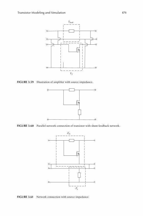
171Transistor Modeling and Simulation
Yfeed
YT
FIGURE 3.59 Illustration of amplifier with source impedance.
FIGURE 3.60 Parallel network connection of transistor with shunt feedback network.
Zt1
Zs
FIGURE 3.61 Network connection with source impedance.
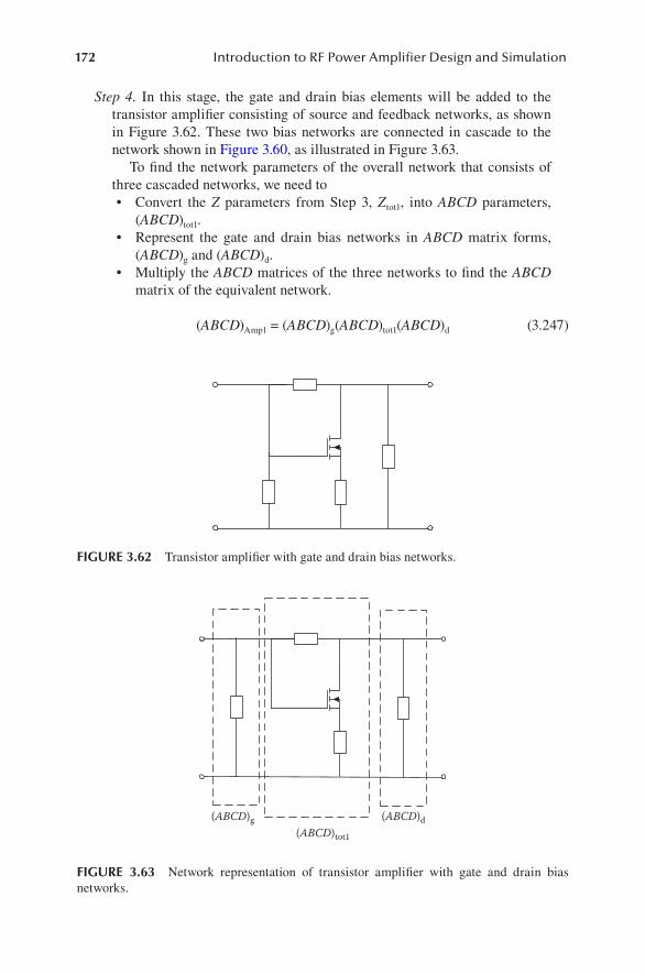
172 Introduction to RF Power Amplifier Design and Simulation
Step 4. In this stage, the gate and drain bias elements will be added to the transistor amplifier consisting of source and feedback networks, as shown in Figure 3.62. These two bias networks are connected in cascade to the network shown in Figure 3.60, as illustrated in Figure 3.63.
To find the network parameters of the overall network that consists of three cascaded networks, we need to• Convert the Z parameters from Step 3, Ztot1, into ABCD parameters,
(ABCD) tot1.• Represent the gate and drain bias networks in ABCD matrix forms,
(ABCD)g and (ABCD)d.• Multiply the ABCD matrices of the three networks to find the ABCD
matrix of the equivalent network.
(ABCD)Amp1 = (ABCD)g(ABCD)tot1(ABCD)d (3.247)
FIGURE 3.62 Transistor amplifier with gate and drain bias networks.
(ABCD)g (ABCD)d(ABCD)tot1
FIGURE 3.63 Network representation of transistor amplifier with gate and drain bias networks.
173Transistor Modeling and Simulation
Step 5. The input and output matching networks are now included to the ampli-fier network shown in Figure 3.62, as illustrated in Figure 3.64.
The input and output matching networks are connected in cascade to the network shown in Step 4, as illustrated in Figure 3.65.
The transistor amplifier network representation with all the networks can be found by• Representing the input and output matching networks in ABCD matrix
forms, (ABCD)IM and (ABCD)OM.• Multiplying the ABCD matrices of the three networks to find the ABCD
matrix of the equivalent network.
( ) ( ) ( ) ( )ABCD ABCD ABCD ABCDAMPtot IM Amp OM= 1 (3.248)
FIGURE 3.64 Transistor amplifier with all the networks including matching networks.
(ABCD)IM (ABCD)OM(ABCD)Amp1
FIGURE 3.65 Network representation of transistor amplifier with all the networks includ-ing matching networks.
174 Introduction to RF Power Amplifier Design and Simulation
Step 6. In this final stage, the transistor amplifier response is found by con-verting the ABCD matrix in Step 5, (ABCD)AMPtot, to a scattering matrix to obtain the complete amplifier response using the parameters including• Maximum available gain• Transducer power gain• Mismatch losses• Stability factor• Unilateral figure of merit
3.8 EXTRACTION OF PARASITICS FOR MOSFET DEVICES
The intrinsic and extrinsic parasitics of MOSFETs are critical to the device and, as a result, amplifier performance because extrinsic effects such as parasitic capaci-tances and inductances cannot be ignored at high frequencies. Hence, the extraction of these parameters is important so that they can be included in the design of RF amplifiers. An example of a widely used RF power transistor package, TO-247, is illustrated in Figure 3.66. The packaged device is treated as a two-port RF network with a peripheral circuit of lumped parasitic elements.
The simplified model showing extrinsic and intrinsic parameters of this device is shown in Figure 3.67. The illustration of the MOSFET equivalent with intrin-sic parameters only is given in Figure 3.68. The complete model with package and intrinsic parasitics for MOSFETs is illustrated in Figure 3.69. It can be shown that under zero bias conditions, VGS = VDS = 0, the device amplifier properties, gm = 0, Rds = ∞, and inductance effects can then be ignored.
Hence, at zero bias, the network-measured S parameters are dominated by capaci-tances, and hence, the small-signal two-port network reduces to the circuit in Figure 3.70. The package parasitic resistances can be found by converting S parameters to Z parameters. The real party of the Z parameters is equal to the package inductance resistance values as given by
ReZ11 = Rg + Rs (3.249)
ReZ22 = Rd + Rs (3.250)
ReZ21 = ReZ21 = Rs (3.251)
FIGURE 3.66 MOSFET TO-247 transistor package.
175Transistor Modeling and Simulation
Ld
Lg
Ls
Cgd
Cgs
CdsG
D
S
FIGURE 3.67 Illustration of extrinsic and intrinsic parameters of TO-247 transistor package.
Cgd
Cgs
Rgs
Rds Cds
Gate Drain
Source
gmVGS
Intrinsic model
FIGURE 3.68 MOSFET package parasitics with intrinsic parameters.
176 Introduction to RF Power Amplifier Design and Simulation
Frequency change does not affect the parasitic resistance values obtained in Equations 3.249 through 3.257. Z parameters, ZDUT, are the parameters measured with zero bias as described before. After parasitic resistances are identified using Equations 3.249 through 3.251, the device-intrinsic parameter Zi is found from
Z Z R R11 11
i DUTg s= − +( ) (3.252)
Z Z R R22 22i DUT
d s= − +( ) (3.253)
Z Z R12 12i DUT
s= − (3.254)
Z Z R21 21i DUT
s= − (3.255)
Lg Ld
Cgs
Cgd
Cds
DG
SLs
S
Rg
gmVgsRds
Rd
Rs
FIGURE 3.69 Small-signal two-port network representation of MOSFETs with parasitics.
Cgd
Cgs Cds
G D
S
Rg Rd
S
Rs
FIGURE 3.70 Zero-biased, small-signal two-port network at low frequencies.

177Transistor Modeling and Simulation
The Y parameters of the intrinsic MOSFET components, Y i, can be obtained from
YZ
ii
=1
(3.256)
or using the conversion parameters given previously. Y parameters can be obtained as
Y j C C11i
gs gd= +ω( ) (3.257)
Y j C CR221i
gd dsds
= + +ω( ) (3.258)
Y j C12i
gd= − ω( ) (3.259)
Y g j C21i
m gd= − ω (3.260)
Hence, the MOSFET intrinsic parameters are
CY
fgd
i
=− ( )Im 12
2π (3.261)
CY Y
fgs
i i
=( ) + ( )Im Im11 12
2π (3.262)
CY Y
fds
i i
=( ) + ( )Im Im22 12
2π (3.263)
RY
ds i= ( )
1
22Re (3.264)
g e Y Yjm
i i− = −ωτ21 12 (3.265)
where
g Y Ymi i= −21 12 (3.266)
τπ
=
− −
−tanIm
Re1 21 12
21 12
2
Y Y
Y Y
f
i i
i i
(3.267)
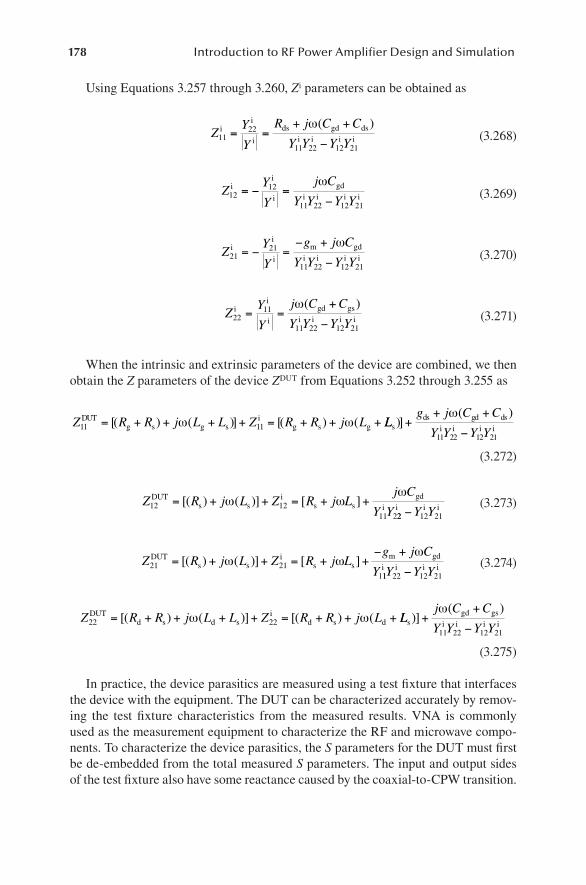
178 Introduction to RF Power Amplifier Design and Simulation
Using Equations 3.257 through 3.260, Zi parameters can be obtained as
ZY
Y
R j C C
Y Y Y Y11
22
11 22 12 21
ii
i
ds gd dsi i i i
= =+ +
−
ω( ) (3.268)
ZY
Y
j C
Y Y Y Y12
12
11 22 12 21
ii
i
gdi i i i
= − =−
ω (3.269)
ZY
Y
g j C
Y Y Y Y21
21
11 22 12 21
ii
i
m gdi i i i
= − =− +
−
ω (3.270)
ZY
Y
j C C
Y Y Y Y22
11
11 22 12 21
ii
i
gd gsi i i i
= =+
−
ω( ) (3.271)
When the intrinsic and extrinsic parameters of the device are combined, we then obtain the Z parameters of the device ZDUT from Equations 3.252 through 3.255 as
Z R R j L L Z R R j L11 11DUT
g s g si
g s g= + + + + = + + +[( ) ( )] [( ) (ω ω LLg j C C
Y Y Y Ys
ds gd dsi i i i
)]( )
++ +
−
ω
11 22 12 21 (3.272)
Z R j L Z R j Lj C
Y Y12 12
11 2
DUTs s
is s
gdi
= + + = + +[( ) ( )] [ ]ω ωω
22 12 21i i i−Y Y
(3.273)
Z R j L Z R j Lg j C
Y21 21
1
DUTs s
is s
m gd= + + = + +− +
[( ) ( )] [ ]ω ωω
11 22 12 21i i i iY Y Y−
(3.274)
Z R R j L L Z R R j L22 22DUT
d s d si
d s d= + + + + = + + +[( ) ( )] [( ) (ω ω LLj C C
Y Y Y Ys
gd gsi i i i
)]( )
++
−
ω
11 22 12 21 (3.275)
In practice, the device parasitics are measured using a test fixture that interfaces the device with the equipment. The DUT can be characterized accurately by remov-ing the test fixture characteristics from the measured results. VNA is commonly used as the measurement equipment to characterize the RF and microwave compo-nents. To characterize the device parasitics, the S parameters for the DUT must first be de-embedded from the total measured S parameters. The input and output sides of the test fixture also have some reactance caused by the coaxial-to-CPW transition.

179Transistor Modeling and Simulation
Design Example
A manufacturer gives the following measured S parameters for the high-power TO-247 MOSFET. It is communicated that
At 3 MHz, low-frequency measurement
S11 = 0.09 − j0.31; S12 = 0.89 + j0.01
S21 = 0.89 + j0.01; S22 = 0.02 − j0.34
At 300 MHz, high-frequency measurement
S11 = −0.35 + j0.76; S12 = 0.2 + j0.1
S21 = 0.2 + j0.1; S22 = −0.4 + j0.85
Calculate the extrinsic and intrinsic parameters of this device by ignoring the test fixture effects. Compare your results with the exact given high-power TO-247 MOSFET extrinsic and intrinsic values, which are
• Ciss = Cgs + Cgd = 2700 pF, Cgs = 2625 pF• Crss = Cgd = 75 pF• Coss = Cds + Cgd = 350 pF, Cds = 275 pF• Lg = 13 nH, Ls = 13 nH, Ld = 5 nH• Rs = 0.95 Ω, Rd = 0.5 Ω, Rg = 5 Ω
Solution
The zero bias MOSFET model given in Figure 3.70 will be used. The follow-ing MATLAB script is written to extract the intrinsic and extrinsic values of the MOSFET using the formulation given by Equations 3.249 through 3.275.
% This program extracts extrinsic and intrinsic parameters of MOSFET% It uses zero bias network with no test fixturing effects.clear;Zo=50; % Enter low and high frequency S parameters fl = input('Enter Low frequency '); fh = input('Enter High frequency '); wl=2*pi*fl; wh=2*pi*fh; s11 _mes = input('Enter S1_11 (Measured S11 in rectangular for Low
Frequency: '); s12 _mes = input('Enter S1_12 (Measured S12 in rectangular for Low
Frequency: '); s21 _mes = input('Enter S1_21 (Measured S21 in rectangular for Low
Frequency: '); s22 _mes = input('Enter S1_22 (Measured S22 in rectangular for Low
Frequency: ');

180 Introduction to RF Power Amplifier Design and Simulation
sc1 1_mes = input('Enter S1_11 (Measured S11 in rectangular for High Frequency: ');
sc1 2_mes = input('Enter S1_12 (Measured S12 in rectangular for High Frequency: ');
sc2 1_mes = input('Enter S1_21 (Measured S21 in rectangular for High Frequency: ');
sc2 2_mes = input('Enter S1_22 (Measured S22 in rectangular for High Frequency: ');
%Convert Zero Bias S parameters to Z parameters [z11,z12,z21,z22]=S2Z(s11_mes,s12_mes,s21_mes,s22_mes,Zo); [y11,y12,y21,y22]=Z2Y(z11,z12,z21,z22);
%Extract Extrinsic Resistances using the formulation %Use Equations 3.232 through 3.234 rd=real(z21) rs=real(z22)-rd rg=real(z11)-rd
%Extract Intrinsic Capacitances using the formulation %Use Equations 3.240 through 3.243 cgs=-imag(y12)/wl cgd=(imag(y11+y12))/wl cds=(imag(y22+y12))/wl
%Convert High Frequency S parameters to Z parameters [z11 ,z12,z21,z22]=S2Z(sc11_mes,sc12_mes,sc21_mes,
sc22_ mes,Zo);
%Extract Extrinsic Inductances using the formulation
Ld=imag(z12)/wh Lg=imag(z11)/wh-Ld Ls=imag(z22)/wh-Ld
%Enter Frequency range f=[1e6:500000:500e6]; w=2*pi*f; %Using the formulation in the book D=-w.^2.*(cgs+cgd).*(cgs+cds)+w.^2.*cgs.^2;Z11=rg+rd+w.*(Lg+Ld)*1i+1i*w.*(cds+cgs)./D;Z12=rd+w.*(Ld)*1i+1i*w.*(cgs)./D;Z21=rd+w.*(Ld)*1i+1i*w.*(cgs)./D;Z22=rs+rd+w.*(Ls+Ld)*1i+1i*w.*(cgd+cgs)./D;
[s11x,s12x,s21x,s22x]=Z2S(Z11,Z12,Z21,Z22,Zo);
smith_chart(2)
for k=1:999
rd1(k)=abs(s11x(k));alpha1(k)=angle(s11x(k));rd2(k)=abs(s12x(k));alpha2(k)=angle(s12x(k));rd3(k)=abs(s22x(k));alpha3(k)=angle(s22x(k));
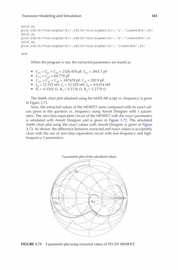
181Transistor Modeling and Simulation
hold onplot(rd1(k)*cos(alpha1(k)),rd1(k)*sin(alpha1(k)),'r','linewidth',10) hold onplot(rd2(k)*cos(alpha2(k)),rd2(k)*sin(alpha2(k)),'k','linewidth',5) hold onplot(rd3(k)*cos(alpha3(k)),rd3(k)*sin(alpha3(k)),'linewidth',15)
end
When the program is run, the extracted parameters are found as
• Ciss = Cgs + Cgd = 2526.478 pF, Cgs = 2461.7 pF• Crss = Cgd = 64.778 pF• Coss = Cds + Cgd = 347.678 pF, Cds = 282.9 pF• Lg = 12.555 nH, Ls = 12.529 nH, Ld = 4.6354 nH• Rs = 0.3502 Ω, Rd = 0.2736 Ω, Rg = 5.2779 Ω
The Smith chart plot obtained using the MATLAB script vs. frequency is given in Figure 3.71.
Now, the extracted values of the MOSFET were compared with its exact val-ues given in the question vs. frequency using Ansoft Designer with S param-eters. The zero bias equivalent circuit of the MOSFET with the exact parameters is simulated with Ansoft Designer and is given in Figure 3.72. The simulated Smith chart plot using the exact values with Ansoft Designer is given in Figure 3.73. As shown, the difference between extracted and exact values is acceptably close with the use of zero bias equivalent circuit with low-frequency and high-frequency S parameters.
S parameter plot of the calculated values
S11
S22 S12
FIGURE 3.71 S parameter plot using extracted values of TO-247 MOSFET.
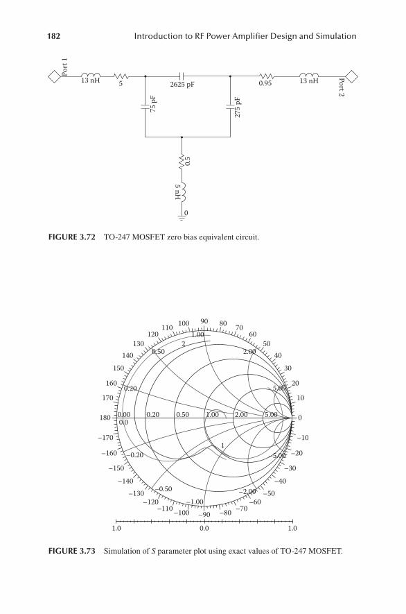
182 Introduction to RF Power Amplifier Design and Simulation
90
–90 –80
80 70
–70–60
6050
2.00
1.00
0.50
0.20
–0.20
–0.50–1.00
–2.00
–5.00
5.00
5.002.001.000.500.200.000.0
–50–40
4030
–30
–20
20
10
–10
0
–100
100
2
110
–110–120
120130
–130–140
140150
–150
–160
160
170
–170
180
1.0 0.0 1.0
1
FIGURE 3.73 Simulation of S parameter plot using exact values of TO-247 MOSFET.
Port
1
75 p
F
13 nH 2625 pF 0.95
275
pF
0.5
5 nH
13 nH
Port 2
5
0
FIGURE 3.72 TO-247 MOSFET zero bias equivalent circuit.
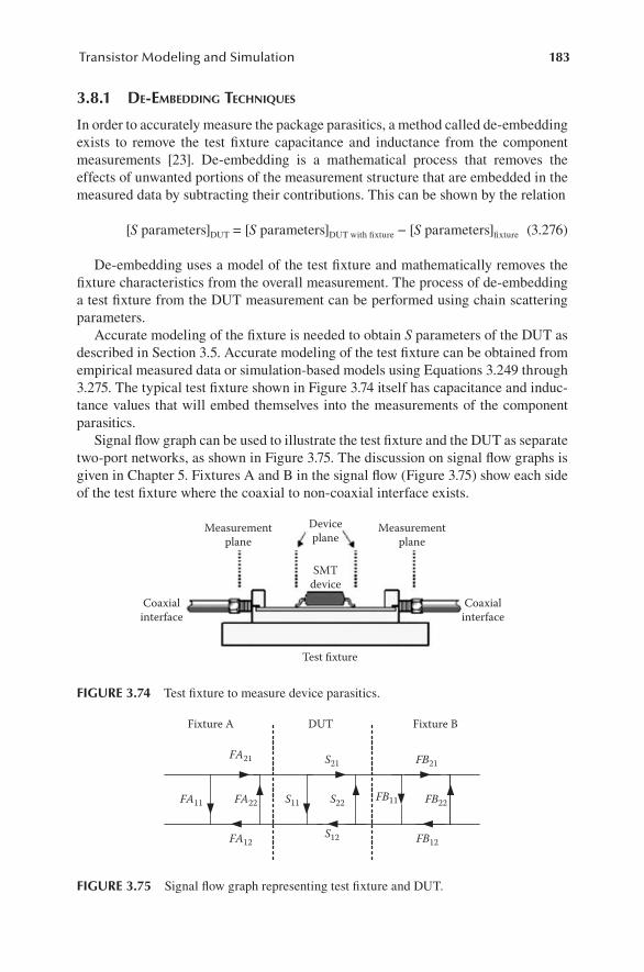
183Transistor Modeling and Simulation
3.8.1 de-embeddIng tecHnIques
In order to accurately measure the package parasitics, a method called de- embedding exists to remove the test fixture capacitance and inductance from the component measurements [23]. De-embedding is a mathematical process that removes the effects of unwanted portions of the measurement structure that are embedded in the measured data by subtracting their contributions. This can be shown by the relation
[S parameters]DUT = [S parameters]DUT with fixture − [S parameters]fixture (3.276)
De-embedding uses a model of the test fixture and mathematically removes the fixture characteristics from the overall measurement. The process of de-embedding a test fixture from the DUT measurement can be performed using chain scattering parameters.
Accurate modeling of the fixture is needed to obtain S parameters of the DUT as described in Section 3.5. Accurate modeling of the test fixture can be obtained from empirical measured data or simulation-based models using Equations 3.249 through 3.275. The typical test fixture shown in Figure 3.74 itself has capacitance and induc-tance values that will embed themselves into the measurements of the component parasitics.
Signal flow graph can be used to illustrate the test fixture and the DUT as separate two-port networks, as shown in Figure 3.75. The discussion on signal flow graphs is given in Chapter 5. Fixtures A and B in the signal flow (Figure 3.75) show each side of the test fixture where the coaxial to non-coaxial interface exists.
Test fixture
SMTdevice
Deviceplane
Measurementplane
Measurementplane
Coaxialinterface
Coaxialinterface
FIGURE 3.74 Test fixture to measure device parasitics.
FA21 S21
S11 S22
S12
Fixture A
FA11
FA12
FA22
DUT
FB21
FB11
FB12
FB22
Fixture B
FIGURE 3.75 Signal flow graph representing test fixture and DUT.
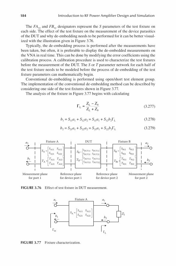
184 Introduction to RF Power Amplifier Design and Simulation
The FAxy and FBxy designators represent the S parameters of the test fixture on each side. The effect of the test fixture on the measurement of the device parasitics of the DUT and why de-embedding needs to be performed for it can be better visual-ized with the illustration given in Figure 3.76.
Typically, the de-embedding process is performed after the measurements have been taken, but often, it is preferable to display the de-embedded measurements on the VNA in real time. This can be done by modifying the error coefficients using the calibration process. A calibration procedure is used to characterize the test fixtures before the measurement of the DUT. The S or T parameter network for each half of the test fixture needs to be modeled before the process of de-embedding of the test fixture parameters can mathematically begin.
Conventional de-embedding is performed using open/short test element group. The implementation of the conventional de-embedding method can be described by considering one side of the test fixtures shown in Figure 3.77.
The analysis of the fixture in Figure 3.77 begins with calculating
ΓLL
L
=−+
Z Z
Z Z0
0
(3.277)
b1 = S11a1 + S12a2 = S11a1 + S12b2ΓL (3.278)
b2 = S21a1 + S22a2 = S21a1 + S22b2ΓL (3.279)
Fixture Aa1
b1
a2
Γin ΓL
b2ZL
SA11SA21
SA12SA22
SA =
FIGURE 3.77 Fixture characterization.
a1
b1
Fixture A DUT Fixture B
Mesurement planefor port 1
Mesurement planefor port 2
Reference planefor device port 1
Reference planefor device port 2
SA11SA21
SA12SA22
SA =
a2
b2TA11TA21
TA12TA22
TA =
SB11SB21
SB12SB22
SB =
TB11TB21
TB12TB22
TBt =
SDUT11SDUT21
SB =
TDUT11TDUT21
SDUT12SDUT22
TDUT12TDUT22
TB =
FIGURE 3.76 Effect of test fixture in DUT measurement.
185Transistor Modeling and Simulation
b2(1 − S22ΓL) = S21a1 (3.280)
bS a
S221 1
221=
−( )ΓL
(3.281)
b S a SS a
S1 11 1 1221 1
221= +
−ΓΓL
L( ) (3.282)
ΓΓΓinL
L
= = +−
ba
SS SS
1
111
12 21
221 (3.283)
Assume that the test fixture is reciprocal, i.e., Z12 = Z21. Then,
ΓΓΓinL
L
= +−
SSS11122
221 (3.284)
To calibrate the test fixture means to find scattering parameters Sij of fixture A. The following three situations are considered:
1. The load is short circuited; ΓL = −1
Γ in,s = −+
SSS11122
221 (3.285)
2. The load is open circuited; ΓL = 1
Γ in,o = +−
SSS11122
221 (3.286)
3. The load is matched; ΓL = 0
Γin = S11 (3.287)
By solving Equations 3.285 through 3.287, we obtain S11, S12, and S22. We then get the scattering parameters Sij of the test fixture. Working with a cascade of three two-port networks, we convert the S parameters of fixtures A and B to the corresponding T parameters. As a result, the overall measurement transmission matrix is
T T
T T
T T
T TAm Am
Am Am
A A
A A
11 12
21 22
11 12
21 22
=T T
T T
T TDUT DUT
DUT DUT
Bm Bm11 12
21 22
11 112
21 22T TBm Bm (3.288)
186 Introduction to RF Power Amplifier Design and Simulation
The T parameters of the DUT are
T T
T T
T T
T TDUT DUT
DUT DUT
A A
A A
11 12
21 22
11 12
21
=
222
1
11 12
21 22
11
−
T T
T T
T TAm Am
Am Am
Bm BBm
Bm Bm
12
21 22
1
T T
−
(3.289)
Finally, the T parameters of the DUT are converted into S parameters.As described, the de-embedding process of the test fixture using the conventional
method [24] is quite involved. This method suffers at high frequencies, mainly due to incompleteness of open and short pattern and approximation of a parasitic circuit by an equivalent circuit topology.
One other alternative is accurate modeling of the test fixtures using electromag-netic (EM) simulators [25,26]. Ansoft High-Frequency Structure Simulator (HFSS) is a 3D EM simulator tool that can be used to model the test fixture that is used to measure the DUT accurately. The test fixture circuit is characterized by the EM simulator and has no approximation and gives accurate results.
The de-embedding process can be done using two techniques: static approach and real-time approach. The details of these methods will be given next.
3.8.2 de-embeddIng tecHnIque wItH statIc approacH
The static approach uses measured data from the VNA, and the de-embedding is performed by processing the data using the T parameter matrix calculations [23]. Once the measurements are de-embedded, the data are displayed statically on a computer screen or can be downloaded into the analyzer’s memory for display. The procedure for de-embedding of the S parameters for the DUT using the static de-embedding method can be outlined as follows:
• Simulate the fixture that will be used to measure the scattering parameters of the DUT and obtain an accurate model.
• Obtain the S parameters of the fixture on the input and output sides from simulation. Convert the S parameters to T parameters.
• Calibrate the VNA with a standard coaxial calibration kit. Measure the combined S parameters of the device and fixture.
• Convert the measured S parameters to T parameters.• Apply the de-embedding equation from
[Tmeas] = [TA][TDUT][TA] (3.290)
from
[TDUT] = [TA]−1[Tmeas][TB]−1 (3.291)
Convert the T parameters of the DUT back to S parameters. This represents the S parameters of the device only; test fixture effects have been removed.
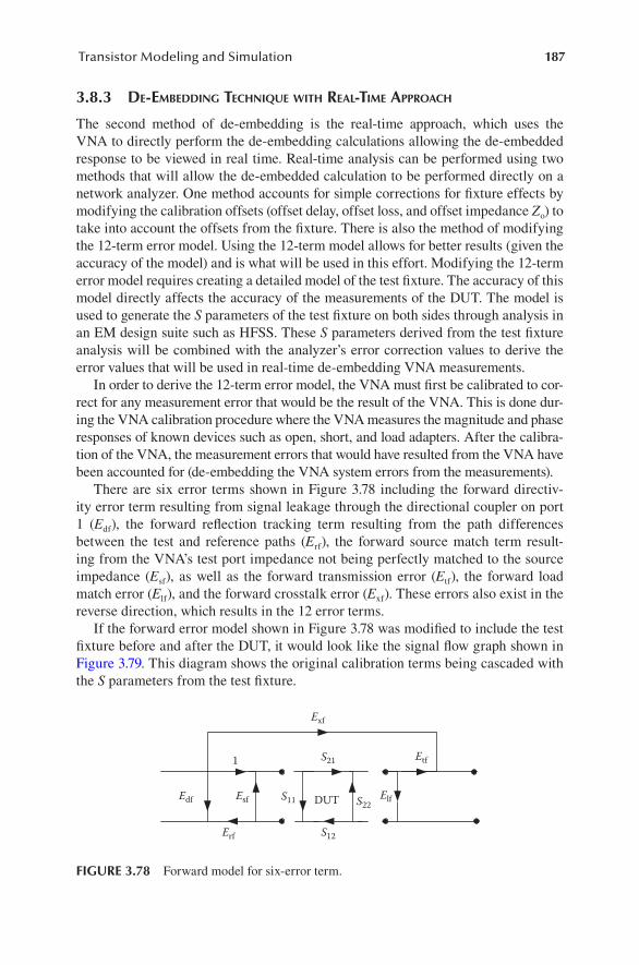
187Transistor Modeling and Simulation
3.8.3 de-embeddIng tecHnIque wItH real-tIme approacH
The second method of de-embedding is the real-time approach, which uses the VNA to directly perform the de-embedding calculations allowing the de-embedded response to be viewed in real time. Real-time analysis can be performed using two methods that will allow the de-embedded calculation to be performed directly on a network analyzer. One method accounts for simple corrections for fixture effects by modifying the calibration offsets (offset delay, offset loss, and offset impedance Zo) to take into account the offsets from the fixture. There is also the method of modifying the 12-term error model. Using the 12-term model allows for better results (given the accuracy of the model) and is what will be used in this effort. Modifying the 12-term error model requires creating a detailed model of the test fixture. The accuracy of this model directly affects the accuracy of the measurements of the DUT. The model is used to generate the S parameters of the test fixture on both sides through analysis in an EM design suite such as HFSS. These S parameters derived from the test fixture analysis will be combined with the analyzer’s error correction values to derive the error values that will be used in real-time de-embedding VNA measurements.
In order to derive the 12-term error model, the VNA must first be calibrated to cor-rect for any measurement error that would be the result of the VNA. This is done dur-ing the VNA calibration procedure where the VNA measures the magnitude and phase responses of known devices such as open, short, and load adapters. After the calibra-tion of the VNA, the measurement errors that would have resulted from the VNA have been accounted for (de-embedding the VNA system errors from the measurements).
There are six error terms shown in Figure 3.78 including the forward directiv-ity error term resulting from signal leakage through the directional coupler on port 1 (Edf), the forward reflection tracking term resulting from the path differences between the test and reference paths (Erf), the forward source match term result-ing from the VNA’s test port impedance not being perfectly matched to the source impedance (Esf), as well as the forward transmission error (Etf), the forward load match error (Elf), and the forward crosstalk error (Exf). These errors also exist in the reverse direction, which results in the 12 error terms.
If the forward error model shown in Figure 3.78 was modified to include the test fixture before and after the DUT, it would look like the signal flow graph shown in Figure 3.79. This diagram shows the original calibration terms being cascaded with the S parameters from the test fixture.
1 S21
S11 S22
S12
Edf
Erf
Esf DUT Elf
Etf
Exf
FIGURE 3.78 Forward model for six-error term.
188 Introduction to RF Power Amplifier Design and Simulation
The cascading of the calibration error terms with the S parameters from the test fixture allows a new signal flow graph to be derived where new error terms exist that include the test fixture S parameters, as shown in Figure 3.80.
Using this new signal flow graph, the error coefficients can be derived and given by Equations 3.292 through 3.302 [23].
′ = +−
E EE FA
E FAdf dfrf
sf
( )( )
11
111 (3.292)
′ = +−
E FAE FA FA
E FAsfsf
sf22
12 21
111( )( )
(3.293)
′ =−
EE FA FA
E FArf
rf
sf
( )
( )12 21
1121
(3.294)
′ = +−
E FBE FB FB
E FBlflf
lf11
12 21
221( )( )
(3.295)
′ =− −
EE FA FB
E FB E FAtftf
lf sf
( )(( )( ))
21 21
22 111 1 (3.296)
′ = +−
E EE FB
E FBdr drrr
sr
( )( )
22
221 (3.297)
1 S21
S11 S22
S12Erf
Edf Esf Elf
Etf
Exf
FA21
Fixture A
FA11
FA12
FA22
DUT
FB21
FB11
FB12
FB22
Fixture B
FIGURE 3.79 Forward model for six-error term with test fixture.
1 S21
S11 S22
S12
Edf
E rf
E sf DUT E lf
E tf
Exf
FIGURE 3.80 Modified forward model for six-error term with test fixture.
189Transistor Modeling and Simulation
′ = +−
E FBE FB FB
E FBsrsr
sr11
12 21
221( )( )
(3.298)
′ = +−
E FAE FA FA
E FAlrlr
lr22
12 21
111( )( )
(3.299)
′ =− −
EE FA FB
E FA E FBtrtr
lr sr
( )(( )( ))
12 12
11 221 1 (3.300)
′ =E Exf xf (3.301)
′ =E Exr xr (3.302)
In Equations 3.292 through 3.302,
Edf = forward (port 1) directivity
Etf = forward (port 1) transmission tracking
Elf = forward (port 1) load match
Exf = forward (port 1) isolation
Erf = forward (port 1) reflection tracking
Esf = forward (port 1) source match
Edr = reverse (port 2) directivity
Err = reverse (port 2) transmission tracking
Elr = reverse (port 2) load match
Exr = reverse (port 2) isolation
Err = reverse (port 2) reflection tracking
Esr = reverse (port 2) source match
Using these derived equations along with the S parameters obtained using model-ing via an EM simulator, we can obtain accurate test results from the VNA.
Design Example
The setup including the test fixture shown in Figure 3.81 is used to measure the MOSFET with TO-247 package considered in the previous example. It is com-municated that the whole setup with the fixture gives the following measured S parameters:
• At 3 MHz, low-frequency measurement
S11 = 0.09 − j0.31; S12 = 0.89 − j0.01
S21 = 0.89 + j0.01; S22 = 0.02 − j0.34
• At 300 MHz, high-frequency measurement
S11 = −0.31 + j0.78; S12 = 0.2 + j0.1
S21 = 0.2 + j0.1; S22 = −0.35 + j0.87
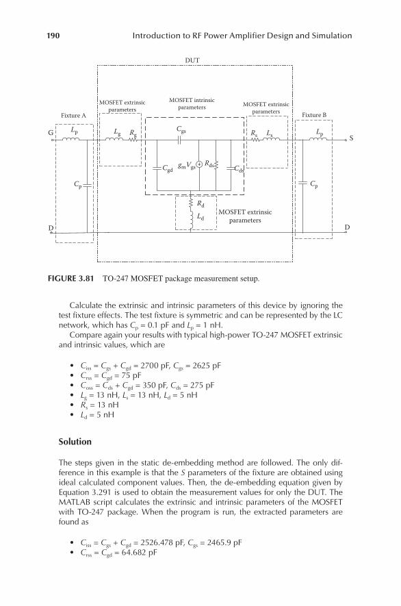
190 Introduction to RF Power Amplifier Design and Simulation
Calculate the extrinsic and intrinsic parameters of this device by ignoring the test fixture effects. The test fixture is symmetric and can be represented by the LC network, which has Cp = 0.1 pF and Lp = 1 nH.
Compare again your results with typical high-power TO-247 MOSFET extrinsic and intrinsic values, which are
• Ciss = Cgs + Cgd = 2700 pF, Cgs = 2625 pF• Crss = Cgd = 75 pF• Coss = Cds + Cgd = 350 pF, Cds = 275 pF• Lg = 13 nH, Ls = 13 nH, Ld = 5 nH• Rs = 13 nH• Ld = 5 nH
Solution
The steps given in the static de-embedding method are followed. The only dif-ference in this example is that the S parameters of the fixture are obtained using ideal calculated component values. Then, the de-embedding equation given by Equation 3.291 is used to obtain the measurement values for only the DUT. The MATLAB script calculates the extrinsic and intrinsic parameters of the MOSFET with TO-247 package. When the program is run, the extracted parameters are found as
• Ciss = Cgs + Cgd = 2526.478 pF, Cgs = 2465.9 pF• Crss = Cgd = 64.682 pF
G
D
S
D
Lp
MOSFET intrinsicparameters
MOSFET extrinsicparameters
MOSFET extrinsicparameters
MOSFET extrinsicparameters
Fixture A Fixture B
DUT
Lg RgCgs
Cgd CdsRdsgmVgs
Cp
LpRs
Rd
Ld
Ls
Cp
FIGURE 3.81 TO-247 MOSFET package measurement setup.
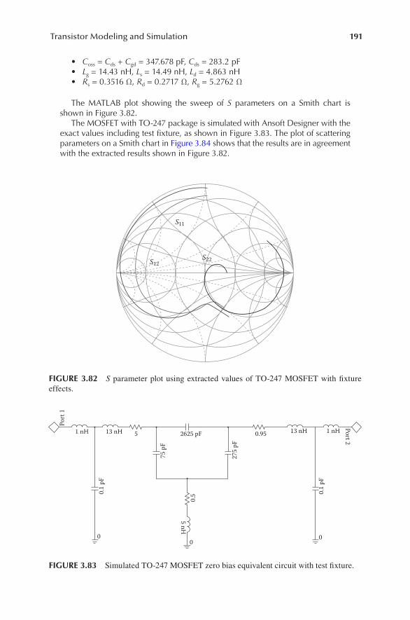
191Transistor Modeling and Simulation
• Coss = Cds + Cgd = 347.678 pF, Cds = 283.2 pF• Lg = 14.43 nH, Ls = 14.49 nH, Ld = 4.863 nH• Rs = 0.3516 Ω, Rd = 0.2717 Ω, Rg = 5.2762 Ω
The MATLAB plot showing the sweep of S parameters on a Smith chart is shown in Figure 3.82.
The MOSFET with TO-247 package is simulated with Ansoft Designer with the exact values including test fixture, as shown in Figure 3.83. The plot of scattering parameters on a Smith chart in Figure 3.84 shows that the results are in agreement with the extracted results shown in Figure 3.82.
S11
S22S12
FIGURE 3.82 S parameter plot using extracted values of TO-247 MOSFET with fixture effects.
Port
1
1 nH 13 nH
75 p
F
275
pF
0.1
pF
0.5 0.
1 pF
5 nH
5 2625 pF 0.95 13 nH 1 nH
Port 2
000
FIGURE 3.83 Simulated TO-247 MOSFET zero bias equivalent circuit with test fixture.
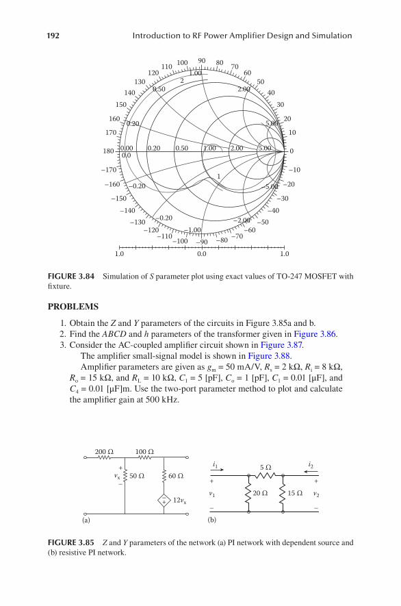
192 Introduction to RF Power Amplifier Design and Simulation
PROBLEMS
1. Obtain the Z and Y parameters of the circuits in Figure 3.85a and b. 2. Find the ABCD and h parameters of the transformer given in Figure 3.86. 3. Consider the AC-coupled amplifier circuit shown in Figure 3.87.
The amplifier small-signal model is shown in Figure 3.88. Amplifier parameters are given as gm = 50 mA/V, Rs = 2 kΩ, Ri = 8 kΩ,
Ro = 15 kΩ, and RL = 10 kΩ, C1 = 5 [pF], Co = 1 [pF], C1 = 0.01 [μF], and C4 = 0.01 [μF]m. Use the two-port parameter method to plot and calculate the amplifier gain at 500 kHz.
200 Ω 100 Ω
50 Ω 60 Ω5 Ω
20 Ω+
–
+
–
15 Ω
+vx
v1 v2
i1 i2
12vx
–
–+
(a) (b)
FIGURE 3.85 Z and Y parameters of the network (a) PI network with dependent source and (b) resistive PI network.
90
–90 –80
80 70
–70–60
6050
2.00
1.00
0.50
0.20
–0.20
–0.20–1.00
–2.00
–5.00
5.00
5.002.001.000.500.200.000.0
–50–40
4030
–30
–20
20
10
–10
0
–100
100
2
110
–110–120
120130
–130–140
140150
–150
–160
160
170
–170
180
1.0 0.0 1.0
1
FIGURE 3.84 Simulation of S parameter plot using exact values of TO-247 MOSFET with fixture.
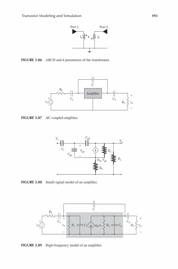
193Transistor Modeling and Simulation
Port 1 Port 2
lt lbk
FIGURE 3.86 ABCD and h parameters of the transformer.
Amplifier +
–
+
–~
CRS
C1 C2vs voRL
FIGURE 3.87 AC-coupled amplifier.
C
+
–
+
–
+
–
~
RS
RL
C2C1C1R1 Ro Co vov1 v1gmvs
FIGURE 3.89 High-frequency model of an amplifier.
Vs Vo
Ro
RS
Gm Vgs
Vgs
+
–Cgs
Ci
RL
Cgd
FIGURE 3.88 Small-signal model of an amplifier.
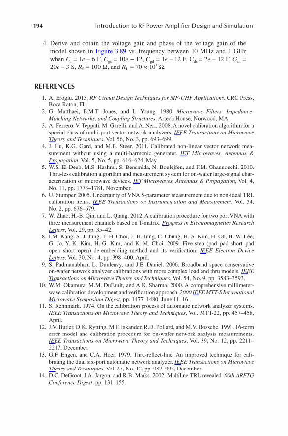
194 Introduction to RF Power Amplifier Design and Simulation
4. Derive and obtain the voltage gain and phase of the voltage gain of the model shown in Figure 3.89 vs. frequency between 10 MHz and 1 GHz when Ci = 1e – 6 F, Cgs = 10e − 12, Cgd = 1e – 12 F, Cds = 2e – 12 F, Gm = 20e – 3 S, RS = 100 Ω, and RL = 70 × 103 Ω.
REFERENCES
1. A. Eroglu. 2013. RF Circuit Design Techniques for MF-UHF Applications. CRC Press, Boca Raton, FL.
2. G. Matthaei, E.M.T. Jones, and L. Young. 1980. Microwave Filters, Impedance-Matching Networks, and Coupling Structures. Artech House, Norwood, MA.
3. A. Ferrero, V. Teppati, M. Garelli, and A. Neri. 2008. A novel calibration algorithm for a special class of multi-port vector network analyzers. IEEE Transactions on Microwave Theory and Techniques, Vol. 56, No. 3, pp. 693–699.
4. J. Hu, K.G. Gard, and M.B. Steer. 2011. Calibrated non-linear vector network mea-surement without using a multi-harmonic generator. IET Microwaves, Antennas & Propagation, Vol. 5, No. 5, pp. 616–624, May.
5. W.S. El-Deeb, M.S. Hashmi, S. Bensmida, N. Boulejfen, and F.M. Ghannouchi. 2010. Thru-less calibration algorithm and measurement system for on-wafer large-signal char-acterization of microwave devices. IET Microwaves, Antennas & Propagation, Vol. 4, No. 11, pp. 1773–1781, November.
6. U. Stumper. 2005. Uncertainty of VNA S-parameter measurement due to non-ideal TRL calibration items. IEEE Transactions on Instrumentation and Measurement, Vol. 54, No. 2, pp. 676–679.
7. W. Zhao, H.-B. Qin, and L. Qiang. 2012. A calibration procedure for two port VNA with three measurement channels based on T-matrix. Progress in Electromagnetics Research Letters, Vol. 29, pp. 35–42.
8. I.M. Kang, S.-J. Jung, T.-H. Choi, J.-H. Jung, C. Chung, H.-S. Kim, H. Oh, H. W. Lee, G. Jo, Y.-K. Kim, H.-G. Kim, and K.-M. Choi. 2009. Five-step (pad–pad short–pad open–short–open) de-embedding method and its verification. IEEE Electron Device Letters, Vol. 30, No. 4, pp. 398–400, April.
9. S. Padmanabhan, L. Dunleavy, and J.E. Daniel. 2006. Broadband space conservative on-wafer network analyzer calibrations with more complex load and thru models. IEEE Transactions on Microwave Theory and Techniques, Vol. 54, No. 9, pp. 3583–3593.
10. W.M. Okamura, M.M. DuFault, and A.K. Sharma. 2000. A comprehensive millimeter- wave calibration development and verification approach. 2000 IEEE MTT-S International Microwave Symposium Digest, pp. 1477–1480, June 11–16.
11. S. Rehnmark. 1974. On the calibration process of automatic network analyzer systems. IEEE Transactions on Microwave Theory and Techniques, Vol. MTT-22, pp. 457–458, April.
12. J.V. Butler, D.K. Rytting, M.F. Iskander, R.D. Pollard, and M.V. Bossche. 1991. 16-term error model and calibration procedure for on-wafer network analysis measurements. IEEE Transactions on Microwave Theory and Techniques, Vol. 39, No. 12, pp. 2211–2217, December.
13. G.F. Engen, and C.A. Hoer. 1979. Thru-reflect-line: An improved technique for cali-brating the dual six-port automatic network analyzer. IEEE Transactions on Microwave Theory and Techniques, Vol. 27, No. 12, pp. 987–993, December.
14. D.C. DeGroot, J.A. Jargon, and R.B. Marks. 2002. Multiline TRL revealed. 60th ARFTG Conference Digest, pp. 131–155.

195Transistor Modeling and Simulation
15. C. Shih. 1998. Advanced TRL (through-reflect-line) fixture design and error analyses for RF high power transistor characterization and automatic load pull measurement. 51st ARFTG Conference Digest, pp. 72–76.
16. R.B. Marks. 1991. A multiline method of network analyzer calibration. IEEE Trans-actions on Microwave Theory and Techniques, Vol. 39, No. 7, pp. 1205–1215.
17. W. Kruppa, and K.F. Sodomsky. 1971. An explicit solution for the scattering param-eters of a linear two-port measured with an imperfect test set (correspondence). IEEE Transactions on Microwave Theory and Techniques, Vol. 19, No. 1, pp. 122–123, January.
18. J. Fitzpatrick. 1978. Error models for system measurements. Microwave Journal, Vol. 21, No. 5, pp. 63–66, May.
19. M. Imparato, T. Weller, and L. Dunleavy. 1999. On-wafer calibration using space con-servative (SOLT) standards. 1999 IEEE MTT-S Int’l Microwave Symposium, Vol. 4, pp. 1643–1646, June.
20. S. Padmanabhan, P. Kirby, J. Daniel, and L. Dunleavy. 2003. Accurate broadband on wafer SOLT calibrations with complex load and thru models. 61st ARFTG Conference Digest, June.
21. B.C. Wadell. 1991. Transmission Line Design Handbook. Artech House, Norwood, MA. 22. I. Wolf. 2006. Coplanar Microwave Integrated Circuits. Wiley, New York. 23. Agilent Technologies. 2004. Agilent de-embedding and embedding S-parameter net-
works using a vector network analyzer. Application Note 1364-1. 24. M.C.A.M. Koolen, J.A.M. Geelen, and M.P.J.G. Versleijen. 1991. An improved de-
embedding technique for on-wafer high-frequency characterization. Proceedings of the IEEE, Bipolar/BiCMOS Circuits and Technology Meeting, pp. 188–191, September.
25. T. Hirano, J. Hirokawa, M. Ando, H. Nakano, and Y. Hirachi. 2008. De-embedding of lumped element characteristics with the aid of EM analysis. Digest of IEEE AP-S International Symposium and USNC/URSI National Radio Science Meeting, Session: 436.3, July 5–12.
26. T. Hirano, H. Nakano, Y. Hirachi, J. Hirokawa, and M. Ando. 2010. De-embedding method using an electromagnetic simulator for characterization of transistors in the millimeter- wave band. IEEE Transactions on Microwave Theory and Techniques, Vol. 58, No. 10, pp. 2663–2672.

197
Resonator Networks for Amplifiers
4.1 INTRODUCTION
Resonators have frequency characteristics that give them the ability to present spe-cific impedance, quality factor, and bandwidth. They can eliminate the reactive component effects and introduce only the resistive portion of the impedance at a frequency called resonance frequency. The circuit that is capable of producing these effects is called a resonant circuit. An ideal resonant circuit acts like a filter and eliminates the unwanted signal content out of the frequency of interest, as shown in Figure 4.1. Resonant circuits can also be used as part of the impedance match-ing networks to transform one impedance at one point to another impedance. In RF amplifier circuits, it is a commonly used technique to present a matched impedance at one frequency and introduce high impedance levels at others. When the amplifier is matched at the input and output for maximum gain, it is possible to deliver the highest amount of power by keeping the circuit stable. The stability of the circuit is accomplished most of the time by using filters and resonators to eliminate the spuri-ous contents and oscillations.
In this chapter, a discussion on resonant networks, transmission lines, Smith chart, and impedance matching networks is given.
4.2 PARALLEL AND SERIES RESONANT NETWORKS
4.2.1 Parallel resonance
Consider the parallel resonant circuit given in Figure 4.2. The response of the circuit can be obtained by finding the voltage with an application of Kirchhoff’s current law (KCL). Application of KCL gives the first-order differential equation for voltage v as
vR L
v I Cvt
t
+ + + =∫1
00
dddoτ
(4.1)
where Io is the initial charged current on the inductor. Equation 4.1 can be written as
d
d
dd
2
2
10
v
t RCvt
vLC
+ + =
(4.2)
4
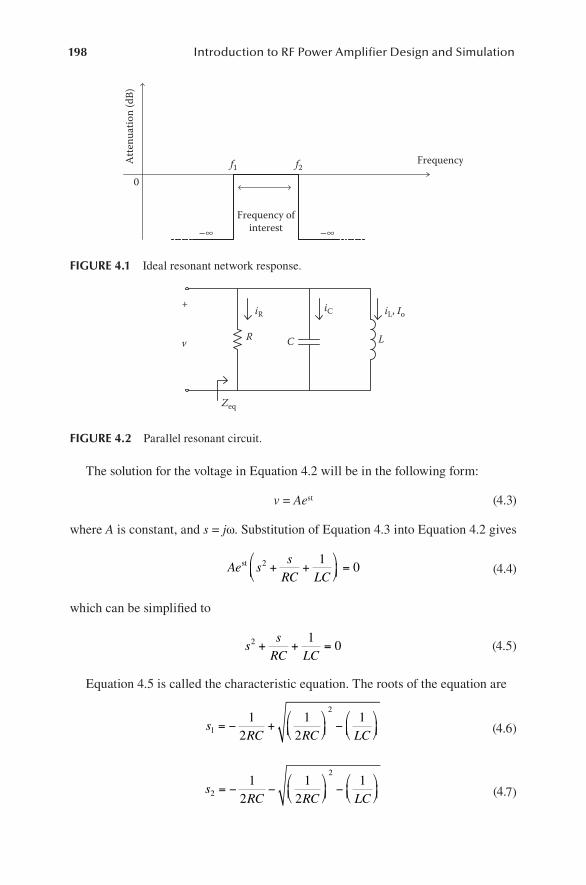
198 Introduction to RF Power Amplifier Design and Simulation
The solution for the voltage in Equation 4.2 will be in the following form:
v = Aest (4.3)
where A is constant, and s = jω. Substitution of Equation 4.3 into Equation 4.2 gives
Ae ssRC LC
st 2 10+ + = (4.4)
which can be simplified to
ssRC LC
2 10+ + = (4.5)
Equation 4.5 is called the characteristic equation. The roots of the equation are
sRC RC LC1
21
21
21
= − +
−
(4.6)
sRC RC LC2
21
21
21
= − −
−
(4.7)
Atte
nuat
ion
(dB)
Frequency ofinterest–∞ –∞
f1 f2 Frequency
0
FIGURE 4.1 Ideal resonant network response.
LCR
+
v
Zeq
iR iC iL, Io
FIGURE 4.2 Parallel resonant circuit.
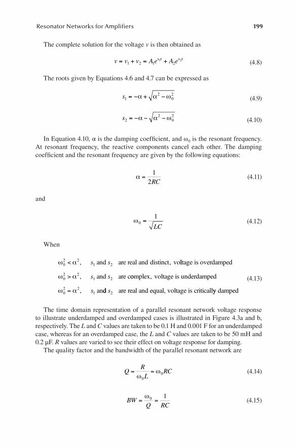
199Resonator Networks for Amplifiers
The complete solution for the voltage v is then obtained as
v v v A e A e= + = +1 2 1 21 2s t s t
(4.8)
The roots given by Equations 4.6 and 4.7 can be expressed as
s12
02= − + −α α ω (4.9)
s22
02= − − −α α ω (4.10)
In Equation 4.10, α is the damping coefficient, and ω0 is the resonant frequency. At resonant frequency, the reactive components cancel each other. The damping coefficient and the resonant frequency are given by the following equations:
α =1
2RC (4.11)
and
ω01
=LC
(4.12)
When
ω α02 2
1 2< , ,are real vos sand and distinct lltage is overdamped
are cω α02 2
1 2> , s sand oomplex voltage is underdamped,
,ω α02 2
1= s andd s2 are real and equal, voltage is criticallyy damped
(4.13)
The time domain representation of a parallel resonant network voltage response to illustrate underdamped and overdamped cases is illustrated in Figure 4.3a and b, respectively. The L and C values are taken to be 0.1 H and 0.001 F for an underdamped case, whereas for an overdamped case, the L and C values are taken to be 50 mH and 0.2 μF. R values are varied to see their effect on voltage response for damping.
The quality factor and the bandwidth of the parallel resonant network are
QRL
RC= =ω
ω0
0 (4.14)
BWQ RC
= =ω0 1
(4.15)
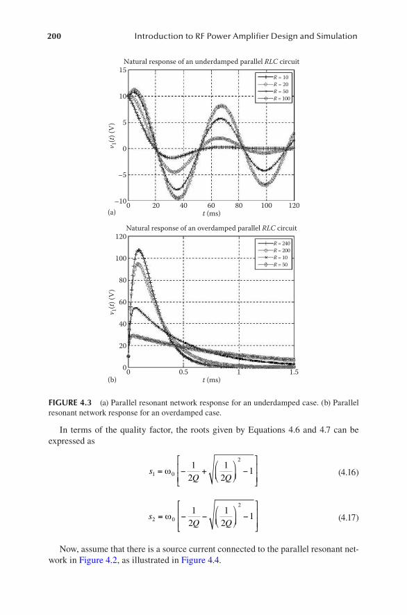
200 Introduction to RF Power Amplifier Design and Simulation
In terms of the quality factor, the roots given by Equations 4.6 and 4.7 can be expressed as
sQ Q1 0
212
12
1= − +
−
ω (4.16)
sQ Q2 0
212
12
1= − −
−
ω (4.17)
Now, assume that there is a source current connected to the parallel resonant net-work in Figure 4.2, as illustrated in Figure 4.4.
15
10
R = 10R = 20R = 50R = 100
5
0
–5
–100 20 40 60t (ms)
v 1(t)
(V)
80 100 120
120
100
80
60
40
20
00 0.5t (ms)
Natural response of an overdamped parallel RLC circuit
Natural response of an underdamped parallel RLC circuit
(a)
(b)
v 1(t)
(V)
1 1.5
R = 240R = 200R = 10R = 50
FIGURE 4.3 (a) Parallel resonant network response for an underdamped case. (b) Parallel resonant network response for an overdamped case.
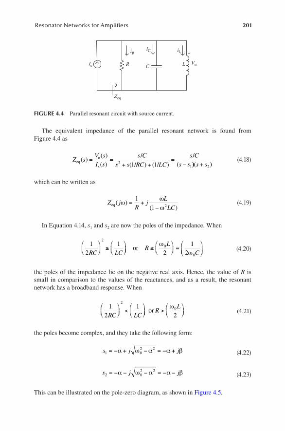
201Resonator Networks for Amplifiers
The equivalent impedance of the parallel resonant network is found from Figure 4.4 as
Z sV sI s
s C
s s RC LC
s Cs seq
o
s
( )( )( ) ( ) ( ) (
= =+ +
=−
/
/ /
/2
11 1 ))( )s s+ 2
(4.18)
which can be written as
Z jR
jL
LCeq ( )
( )ω
ω
ω= +
−
1
1 2 (4.19)
In Equation 4.14, s1 and s2 are now the poles of the impedance. When
1
21
21
2
2
0
0RC LCR
LC
≥
≤
=
or
ωω
(4.20)
the poles of the impedance lie on the negative real axis. Hence, the value of R is small in comparison to the values of the reactances, and as a result, the resonant network has a broadband response. When
1
21
2
2
0
RC LCR
L
<
>
or
ω (4.21)
the poles become complex, and they take the following form:
s j j1 02 2= − + − = − +α ω α α β (4.22)
s j j2 02 2= − − − = − −α ω α α β (4.23)
This can be illustrated on the pole-zero diagram, as shown in Figure 4.5.
LCR
+
Vo
Zeq
iRiC iL
Is
FIGURE 4.4 Parallel resonant circuit with source current.
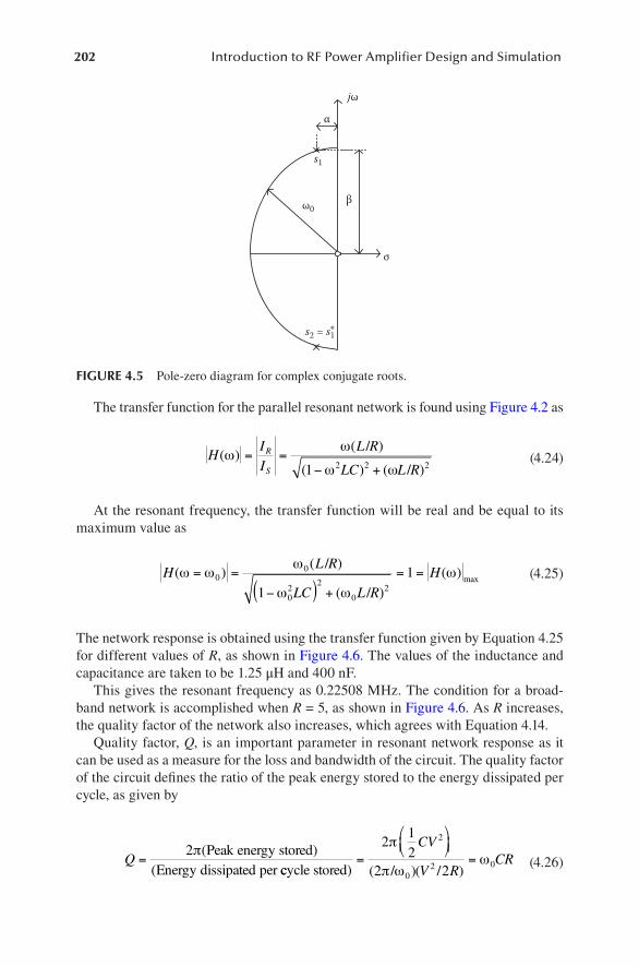
202 Introduction to RF Power Amplifier Design and Simulation
The transfer function for the parallel resonant network is found using Figure 4.2 as
HII
L R
LC L R
R
S
( )( )
( ) ( )ω
ω
ω ω= =
− +
/
/1 2 2 2
(4.24)
At the resonant frequency, the transfer function will be real and be equal to its maximum value as
HL R
LC L R
H( )( )
( )( ) maxω ω
ω
ω ωω= =
−( ) += =0
0
02
2
021
1/
/
(4.25)
The network response is obtained using the transfer function given by Equation 4.25 for different values of R, as shown in Figure 4.6. The values of the inductance and capacitance are taken to be 1.25 μH and 400 nF.
This gives the resonant frequency as 0.22508 MHz. The condition for a broad-band network is accomplished when R = 5, as shown in Figure 4.6. As R increases, the quality factor of the network also increases, which agrees with Equation 4.14.
Quality factor, Q, is an important parameter in resonant network response as it can be used as a measure for the loss and bandwidth of the circuit. The quality factor of the circuit defines the ratio of the peak energy stored to the energy dissipated per cycle, as given by
Q =2π(
(Peak energy stored)
Energy dissipated per ccycle stored) / /=
=2
12
2 2
2
02 0
π
π ωω
CV
V RCR
( )( ) (4.26)
s1
s2 = s1*
ω0
jω
α
β
σ
FIGURE 4.5 Pole-zero diagram for complex conjugate roots.
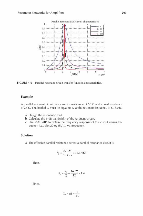
203Resonator Networks for Amplifiers
Example
A parallel resonant circuit has a source resistance of 50 Ω and a load resistance of 25 Ω. The loaded Q must be equal to 12 at the resonant frequency of 60 MHz.
a. Design the resonant circuit. b. Calculate the 3-dB bandwidth of the resonant circuit. c. Use MATLAB® to obtain the frequency response of this circuit versus fre-
quency, i.e., plot 20log (Vo/Vin) vs. frequency.
Solution
a. The effective parallel resistance across a parallel resonance circuit is
Rp = +
=( )
. [ ]50 2550 25
16 67 Ω
Then,
X
R
Qpp= = =
16 6712
1 4.
.
Since,
X L
Cp = =ωω1
1R = 5R = 20R = 50R = 300
0.9
0.8
0.7
0.6
0.5
0.4
0.3
0.2
0.1
00 1 2 3 4f (Hz)
Parallel resonant RLC circuit characteristics
|H(ω
)|
5 6 7× 10⁵
FIGURE 4.6 Parallel resonant circuit transfer function characteristics.
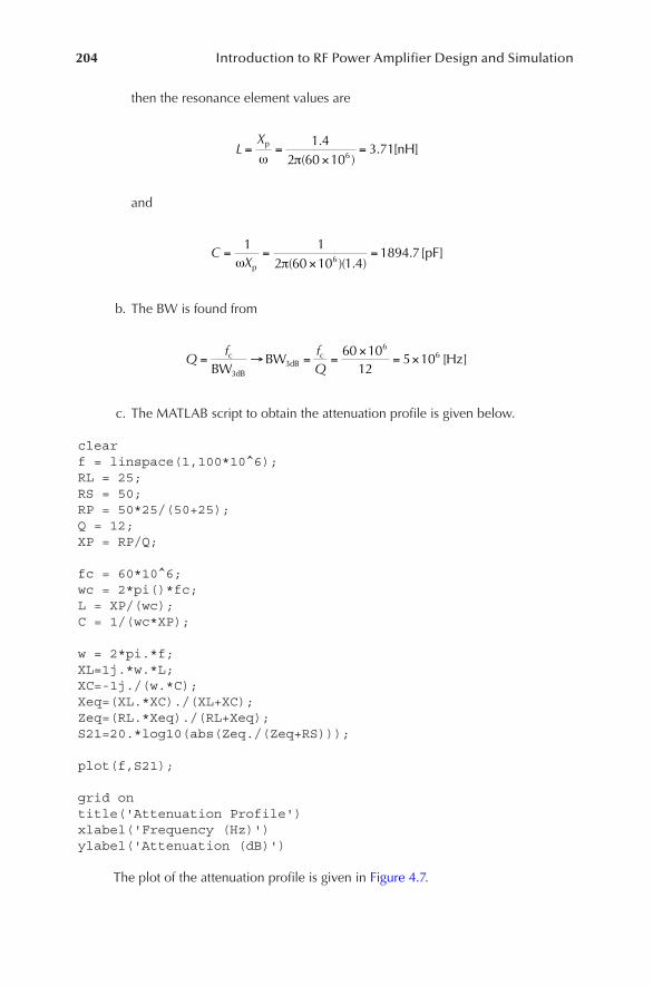
204 Introduction to RF Power Amplifier Design and Simulation
then the resonance element values are
L
X= =
×=p nH
ω π
1 42 60 10
3 716
.( )
. [ ]
and
CX
= =×
=1 1
2 60 10 1 41894 76ω πp
pF( )( . )
. [ ]
b. The BW is found from
Q
fQ
= → = =×
= ×fc
dBdB
c
BWBW Hz
33
6660 10
125 10 [ ]
c. The MATLAB script to obtain the attenuation profile is given below.
clearf = linspace(1,100*10^6);RL = 25;RS = 50;RP = 50*25/(50+25);Q = 12;XP = RP/Q;
fc = 60*10^6;wc = 2*pi()*fc;L = XP/(wc);C = 1/(wc*XP);
w = 2*pi.*f;XL=1j.*w.*L;XC=-1j./(w.*C);Xeq=(XL.*XC)./(XL+XC);Zeq=(RL.*Xeq)./(RL+Xeq);S21=20.*log10(abs(Zeq./(Zeq+RS)));
plot(f,S21);
grid ontitle('Attenuation Profile')xlabel('Frequency (Hz)')ylabel('Attenuation (dB)')
The plot of the attenuation profile is given in Figure 4.7.
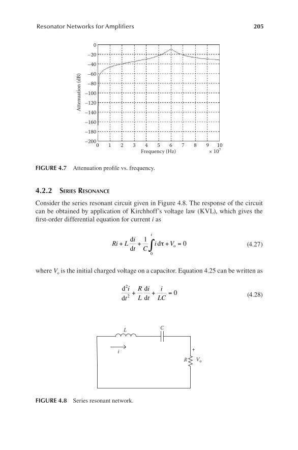
205Resonator Networks for Amplifiers
4.2.2 series resonance
Consider the series resonant circuit given in Figure 4.8. The response of the circuit can be obtained by application of Kirchhoff’s voltage law (KVL), which gives the first-order differential equation for current i as
Ri Lit C
i V
t
+ + + =∫dd
d1
00
τ o (4.27)
where Vo is the initial charged voltage on a capacitor. Equation 4.25 can be written as
d
d
dd
2
20
i
t
RL
it
iLC
+ + = (4.28)
0
–20
–40
–60
–80
–100
–120
–140
–160
–180
–2000 1 2 3 4 5
Frequency (Hz) × 107
Atte
nuat
ion
(dB)
6 7 8 9 10
FIGURE 4.7 Attenuation profile vs. frequency.
L C
R
+
Vo
i
FIGURE 4.8 Series resonant network.
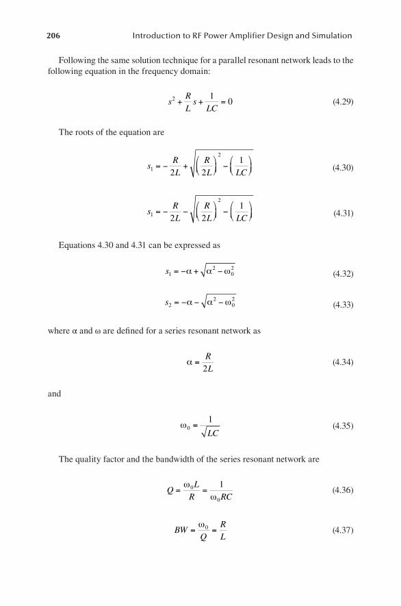
206 Introduction to RF Power Amplifier Design and Simulation
Following the same solution technique for a parallel resonant network leads to the following equation in the frequency domain:
sRLs
LC2 1
0+ + = (4.29)
The roots of the equation are
sRL
RL LC1
2
2 21
= − +
−
(4.30)
sRL
RL LC1
2
2 21
= − −
−
(4.31)
Equations 4.30 and 4.31 can be expressed as
s12
02= − + −α α ω (4.32)
s22
02= − − −α α ω (4.33)
where α and ω are defined for a series resonant network as
α =RL2
(4.34)
and
ω01
=LC
(4.35)
The quality factor and the bandwidth of the series resonant network are
QLR RC
= =ω
ω0
0
1 (4.36)
BWQ
RL
= =ω0 (4.37)
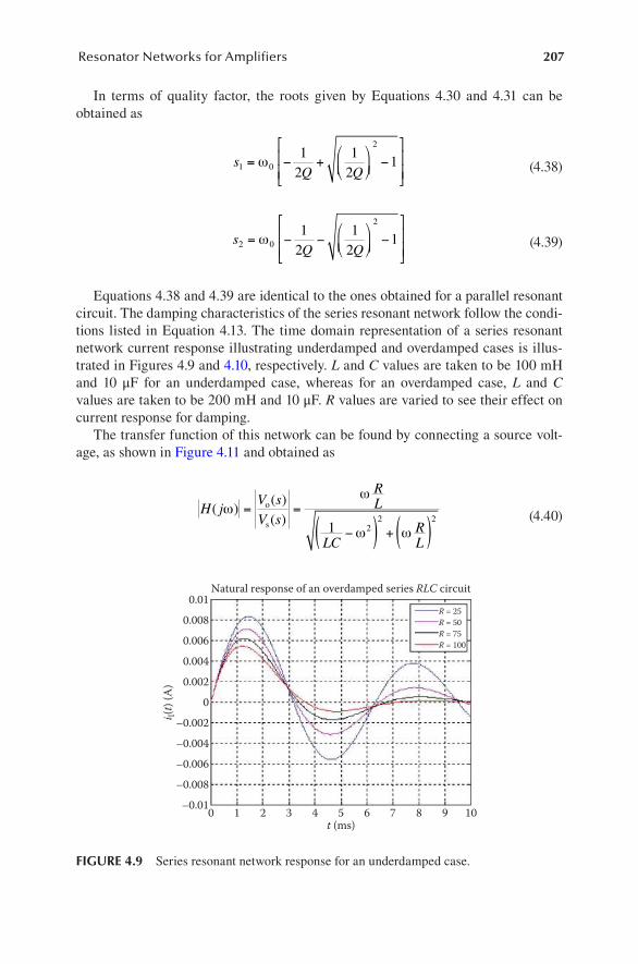
207Resonator Networks for Amplifiers
In terms of quality factor, the roots given by Equations 4.30 and 4.31 can be obtained as
sQ Q1 0
212
12
1= − +
−
ω
(4.38)
sQ Q2 0
212
12
1= − −
−
ω
(4.39)
Equations 4.38 and 4.39 are identical to the ones obtained for a parallel resonant circuit. The damping characteristics of the series resonant network follow the condi-tions listed in Equation 4.13. The time domain representation of a series resonant network current response illustrating underdamped and overdamped cases is illus-trated in Figures 4.9 and 4.10, respectively. L and C values are taken to be 100 mH and 10 μF for an underdamped case, whereas for an overdamped case, L and C values are taken to be 200 mH and 10 μF. R values are varied to see their effect on current response for damping.
The transfer function of this network can be found by connecting a source volt-age, as shown in Figure 4.11 and obtained as
H jV sV s
RL
LCRL
( )( )( )
ωω
ω ω
= =
−( ) + ( )o
s 1 22 2
(4.40)
0.01
0.008
0.006
0.004
0.002
–0.002
–0.004
–0.006
–0.008
–0.010 1 2 3 4 5t (ms)
R = 25R = 50R = 75R = 100
Natural response of an overdamped series RLC circuit
i l(t)
(A)
6 7 8 9 10
0
FIGURE 4.9 Series resonant network response for an underdamped case.
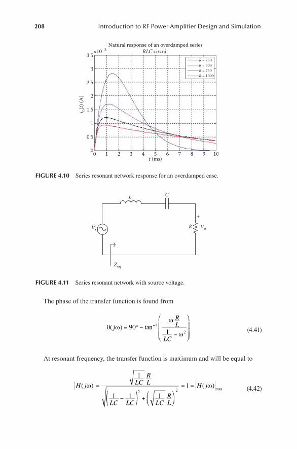
208 Introduction to RF Power Amplifier Design and Simulation
The phase of the transfer function is found from
θ ωω
ω( ) tanj
RL
LC
= −−
−901
1
2°
(4.41)
At resonant frequency, the transfer function is maximum and will be equal to
H j LCRL
LC LC LCRL
H j( ) ( )max
ω ω=
−( ) +
= =
1
1 1 1
12 2
(4.42)
3.5×10⁻³
3
2.5
2
1.5
0.5
1
00 1 2 3 4 5t (ms)
Natural response of an overdamped seriesRLC circuit
6 7 8 9 10
R = 250R = 500R = 750R = 1000
i n(t)
(A)
FIGURE 4.10 Series resonant network response for an overdamped case.
L C
R
+
VoVs
Zeq
FIGURE 4.11 Series resonant network with source voltage.
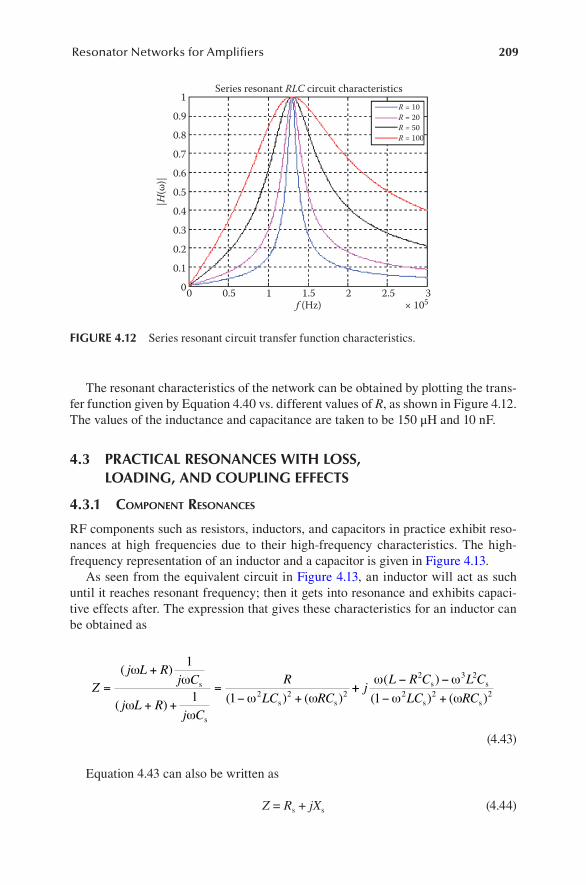
209Resonator Networks for Amplifiers
The resonant characteristics of the network can be obtained by plotting the trans-fer function given by Equation 4.40 vs. different values of R, as shown in Figure 4.12. The values of the inductance and capacitance are taken to be 150 μH and 10 nF.
4.3 PRACTICAL RESONANCES WITH LOSS, LOADING, AND COUPLING EFFECTS
4.3.1 comPonent resonances
RF components such as resistors, inductors, and capacitors in practice exhibit reso-nances at high frequencies due to their high-frequency characteristics. The high-frequency representation of an inductor and a capacitor is given in Figure 4.13.
As seen from the equivalent circuit in Figure 4.13, an inductor will act as such until it reaches resonant frequency; then it gets into resonance and exhibits capaci-tive effects after. The expression that gives these characteristics for an inductor can be obtained as
Zj L R
j C
j L Rj C
R
LC RC=
+
+ +=
− +
( )
( ) ( ) ( )
ωω
ωω
ω ω
1
1 1 2 2 2s
s
s s
++− −
− +j
L R C L C
LC RC
ω ω
ω ω
( )
( ) ( )
2 3 2
2 2 21s s
s s
(4.43)
Equation 4.43 can also be written as
Z = Rs + jXs (4.44)
1
0.9
0.8
0.7
0.6
0.5
0.4
0.3
0.2
0.1
00 0.5 1.5f (Hz)
Series resonant RLC circuit characteristics
|H(ω
)|
× 1052 2.5 31
R = 10R = 20R = 50R = 100
FIGURE 4.12 Series resonant circuit transfer function characteristics.
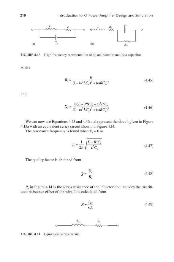
210 Introduction to RF Power Amplifier Design and Simulation
where
RR
LC RCs
s s
=− +( ) ( )1 2 2 2ω ω
(4.45)
and
XL R C L C
LC RCs
s s
s s
=− −
− +
ω ω
ω ω
( )
( ) ( )
2 3 2
2 2 21 (4.46)
We can now use Equations 4.45 and 4.46 and represent the circuit given in Figure 4.13a with an equivalent series circuit shown in Figure 4.14.
The resonance frequency is found when Xs = 0 as
fL R C
L Cr
s
s
=−1
2
2
2π (4.47)
The quality factor is obtained from
QX
R= s
s
(4.48)
Rs in Figure 4.14 is the series resistance of the inductor and includes the distrib-uted resistance effect of the wire. It is calculated from
RlA
= W
σ (4.49)
Ls Rs
FIGURE 4.14 Equivalent series circuit.
L
(a) (b)
R
Cs
L
Rd
CRs
FIGURE 4.13 High-frequency representation of (a) an inductor and (b) a capacitor.
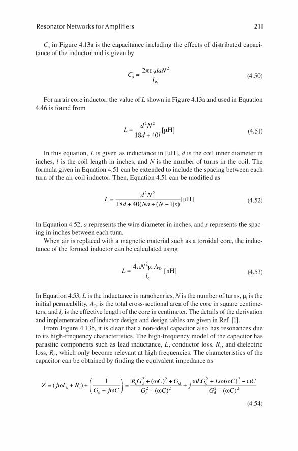
211Resonator Networks for Amplifiers
Cs in Figure 4.13a is the capacitance including the effects of distributed capaci-tance of the inductor and is given by
CdaNlsW
=2 0
2πε (4.50)
For an air core inductor, the value of L shown in Figure 4.13a and used in Equation 4.46 is found from
Ld Nd l
=+
2 2
18 40[ ]µH (4.51)
In this equation, L is given as inductance in [μH], d is the coil inner diameter in inches, l is the coil length in inches, and N is the number of turns in the coil. The formula given in Equation 4.51 can be extended to include the spacing between each turn of the air coil inductor. Then, Equation 4.51 can be modified as
Ld N
d Na N s=
+ + −
2 2
18 40 1( ( ) )[ ]µH (4.52)
In Equation 4.52, a represents the wire diameter in inches, and s represents the spac-ing in inches between each turn.
When air is replaced with a magnetic material such as a toroidal core, the induc-tance of the formed inductor can be calculated using
LN Al
=4 2π µ i Tc
e
nH[ ] (4.53)
In Equation 4.53, L is the inductance in nanohenries, N is the number of turns, μi is the initial permeability, ATc is the total cross-sectional area of the core in square centime-ters, and le is the effective length of the core in centimeter. The details of the derivation and implementation of inductor design and design tables are given in Ref. [1].
From Figure 4.13b, it is clear that a non-ideal capacitor also has resonances due to its high-frequency characteristics. The high-frequency model of the capacitor has parasitic components such as lead inductance, L, conductor loss, Rs, and dielectric loss, Rd, which only become relevant at high frequencies. The characteristics of the capacitor can be obtained by finding the equivalent impedance as
Z j L RG j C
R G C G
G C= + +
+
=
+ +
+( )
( )
(ω
ωω
ωs s
d
s d d
d
1 2 2
2 ))
( )
( )2
2 2
2 2+
+ −
+jLG L C C
G C
ω ω ω ω
ωd
d (4.54)

212 Introduction to RF Power Amplifier Design and Simulation
Then, Equation 4.54 can be expressed as
Z = Rs + jXs (4.55)
where
RR G C G
G Cs
s d d
d
=+ +
+
2 2
2 2
( )
( )
ω
ω (4.56)
XLG L C C
G Cs
d
d
=+ −
+
ω ω ω ω
ω
2 2
2 2
( )
( ) (4.57)
The impedance given in Equation 4.55 can be converted to admittance as
Y ZR
R Xj
X
R XG jB= =
++
−
+= +−1
2 2 2 2s
s s
s
s s
(4.58)
or
YR G C G G C
RG C G=
+ +( ) +( )+ +( ) +
s d d d
s d d
2 2 2 2
2 22
( ) ( )
( )
ω ω
ω ωω ω ω ω
ω ω ω ω ω
LG L C C
jC LG L C G C
d
d d
2 22
2 2 2
+ −( )
+− −( ) +
( )
( ) ( ))
( ) ( )
2
2 22
2 22
( )+ +( ) + + −( )R G C G LG L C Cs d d dω ω ω ω ω
(4.59)
Then, the capacitor can be represented by a parallel equivalent circuit, as shown in Figure 4.15, where
GRG C G G C
RG C G=
+ +( ) +( )+ +( ) +
s d d d
s d d
2 2 2 2
2 22
( ) ( )
( )
ω ω
ω ωω ω ω ωLG L C Cd2 2
2+ −( )( )
(4.60)
BC LG L C G C
R G C G=
− −( ) +( )+ +( )ω ω ω ω ω
ω
d d
s d d
2 2 2 2
2 2
( ) ( )
( )22
2 22
+ + −( )ω ω ω ωLG L C Cd ( ) (4.61)
GCp
FIGURE 4.15 Equivalent parallel circuit.

213Resonator Networks for Amplifiers
The resonance frequency for the circuit shown in Figure 4.14 is found when B = 0 as
fR C L
R C Lr =
−12
2
2 2π (4.62)
The quality factor for the parallel network is then obtained from
QBG
R
X= = p
p
(4.63)
Design Example
Develop a MATLAB graphic user interface (GUI) to design an air core inductor with a user-specified inductance value and with air core diameter. The program should also be able to identify the correct wire gauge for the user-entered current amount. Assume that the operational voltage is 50 [Vrms] and the frequency is 27.12 [MHz]. With your program,
a. Calculate the number of turns. b. Determine the minimum gauge wire that needs to be used. c. Obtain the high-frequency characteristic of the inductor. d. Identify its resonant frequency. e. Find its quality factor. f. Find the length of the wire that will be used. g. Find the length of the inductor.
Solution
The following is the MATLAB GUI that is developed.
clear%Gui Promptprompt = 'Inductance [uH]:','Inductor Inner Diameter [in]: ',... 'Current [A]:';dlg_title = 'Air Core Inductor Parameters';num_lines = 1;def = '0.180','0.25','5';answer = inputdlg(prompt,dlg_title,num_lines,def, 'on');
%convert the strings received from the GUI to numbersvaluearray = str2double(answer);
%Give variable names to the received numbersLnominal=valuearray(1);d=valuearray(2);I=valuearray(3);
%Convert inner diameter to metersdm=d*0.0254;

214 Introduction to RF Power Amplifier Design and Simulation
%Establish the tables of wire gauge, ampacity, and diameter as vectorsawgvector=[40 38 36 34 32 30 28 26 24 22 20 18 16 14 12 10 8 6 4 2 0];ampacityvector=[0.226134423 0.314649454 0.437811623 0.609182742... 0.847633078 1.179419221 1.641075289 2.283435826 3.177233372 ... 4.420887061 6.151339898 8.559138024 11.90941241 16.57107334... 23.05743241 32.08272502 44.64075732 62.11433765 86.42754229 ... 120.2575822 167.3296];wirediametervector=[0.0799 0.101 0.127 0.16 0.202 0.255... 0.321 0.405 0.511 0.644 0.812 1.024 1.291 1.628 ... 2.053 2.588 3.264 4.115 5.189 6.544 8.251];
%Initialize variables for use in the wire size search loopIrating=0;awgselected=0;k=1;flag=0;wirediametermm=0;errorflag=0;
%Start with the smallest wire and see if it meets the required current, %if it does not, go to next size up and repeat, stop when wire is large enoughwhile flag==0 Irating=ampacityvector(k); if I>Irating k=k+1; if k>21 msgbox( sprintf(['The required current exceeds '... 'the rating of all available wire stock'])); errorflag=1; break end elseif I<Irating awgselected=awgvector(k); wirediametermm=wirediametervector(k); flag=1; end end
%Convert wire diameter to incheswirediameterin=wirediametermm*0.0393701;a=wirediameterin;
%Calculate the nominal number of turnsNnominal=max(roots([d^2 -40*a*Lnominal -18*d*Lnominal]));
%Convert turns to an integerN=round(Nnominal);
%Recalculate inductance value based on integer NL=(d^2*N^2)/(18*d+40*N*a)/1e6;
%Calculate length of wire and wire cross-sectional arealw=2*pi*(dm/2)*N;A=pi*(wirediametermm/2000)^2;

215Resonator Networks for Amplifiers
%Total wire resistance assuming copper wireR=lw/((59.6e6)*A); %Total capacitance calculationC=(2*pi*8.84194128e-12*dm*a*0.0254*N^2)/lw; %Axial inductor lengthinductorlength=N*wirediametermm; %Calculate resonant frequencyresonant=1/(2*pi)*sqrt((L-R^2*C)/(L^2*C))/1e6; %Generate high frequency charateristic plot and Q plot, plot f out to 2x%resonant frequency to make each plot consistentfvector=linspace(1,resonant*2,200);Zvector=1:200;Qvector=1:200;j=sqrt(-1);
%Index through vector of frequencies and generate Z and Q at each frequencyfor p=1:200 f=fvector(p); w=2*pi*f*1e6; Zvector(p)=((j*w*L+R)/(j*w*C))/((j*w*L+R)+(1/(j*w*C))); Rs=R/((1-w^2*L*C)^2+(w*R*C)^2); Xs=(w*(L-R^2*C)-(w^3*L^2*C))/((1-w^2*L*C)^2+(w*R*C)^2); Qvector(p)=abs(Xs)/Rs;end %Convert values to proper unit magnitude for displayL=L*1e6;lw=lw*1000;lw_in=lw/25.4;inductorlength_in=N*wirediametermm/25.4;R=R*1000; dmm=d*25.4; %Calculate Inductor value differenceLdiff=(abs(L-Lnominal)/Lnominal)*100; %If Inductor value difference is greater than 10 percent or the inductor length%is greater than 10'', display error if one hasnt already been displayedif (Ldiff>10 && errorflag==0) msgbox( sprintf([ 'The given design parameters result in an Inductance\n'... 'value that is greater than 10 percent from the desired value. \n\n'... 'Try selecting a different Inductor inner diameter.'],Lnominal,d,dmm,I)); errorflag=1;elseif (inductorlength_in>10 && errorflag==0) msgbox( sprintf([

216 Introduction to RF Power Amplifier Design and Simulation
'The given design parameters result in an Inductor\n'... ' with an axial length greater than 10 inches.\n\n'... 'Try selecting a different Inductor inner diameter.'],Lnominal,d,dmm,I)); errorflag=1;end %If there are no design errors, display results and plotsif errorflag==0; subplot(1,2,1) plot(fvector,abs(Zvector)) xlabel('f (MHz)') ylabel('Impedance Magnitude Z') title('High Frequency Inductor Response') subplot(1,2,2) plot(fvector,Qvector) xlabel('f (MHz)') ylabel('Quality Factor Z') title('High Frequency Q Response') msgbox( sprintf([... 'Given design parameters: \n'... ' Nominal Inductance: %4.4f uH \n'... ' Inductor Inner Diameter: %4.3f in, %4.3f mm\n'... ' Rated Current: %4.2f A \n'... '\n'... 'The specifications of the air-core inductor are as follows: \n'... ' Actual Inductance: %6.4f uH\n'... ' Inductance value difference: %4.2f percent\n'... ' Turns: %0.0f \n'... ' Wire Gauge: %0.0f AWG\n'... ' Length of wire: %4.2f in, %4.2f mm\n'... ' (Add extra for connection leads)\n'... ' Axial Length of Inductor: %4.2f in, %4.2f mm\n'... ' Resonant Frequency: %6.2f MHz\n'... ' Series Resistance: %4.3f mohm\n'... '\n'... 'High frequency response and Quality '... 'factor plots are shown in Figure 1\n\n\n']... ,Lnominal,d,dmm,I,L,Ldiff,N,awgselected,... lw_in,lw,inductorlength_in,inductorlength,resonant,R)); end
The program output for an air core inductor with an inductance of 180 [nH] with 0.25-in. diameter, which can handle 5 [Arms], is shown in Figures 4.16 and 4.17.
4.3.2 Parallel lc networks
4.3.2.1 Parallel LC Networks with Ideal ComponentsWhen the ideal components are used, the typical circuit would be represented as the one shown in Figure 4.18. At resonance, the magnitudes of the reactances of the L and C elements are equal. The reactances of the two components have opposite signs
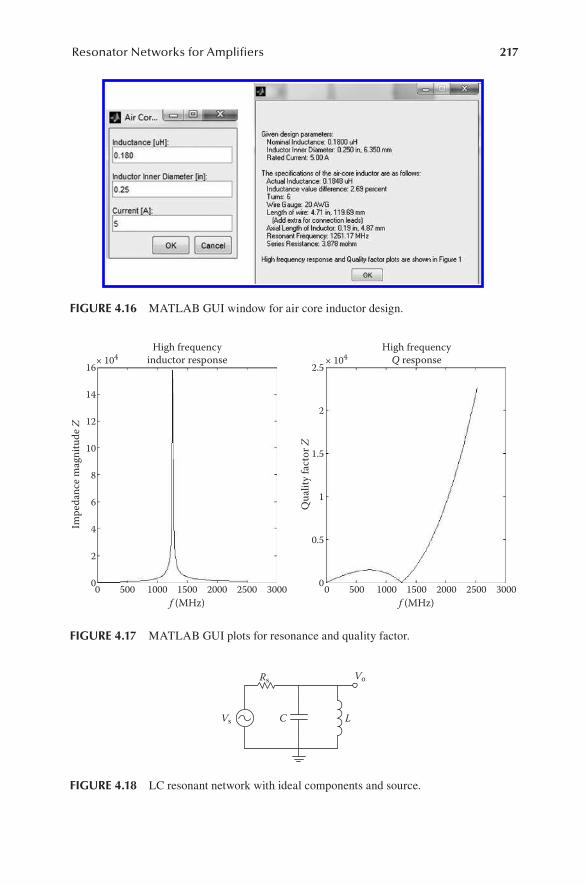
217Resonator Networks for Amplifiers
FIGURE 4.16 MATLAB GUI window for air core inductor design.
16× 104
14
12
10
8
6
4
2
00 500 1000 1500f (MHz)
High frequencyinductor response
Impe
danc
e mag
nitu
de Z
2000 30002500
2.5× 10⁴
2
1.5
1
0.5
00 500 1000 1500f (MHz)
High frequencyQ response
Qua
lity f
acto
r Z
2000 30002500
FIGURE 4.17 MATLAB GUI plots for resonance and quality factor.
Rs
C LVs
Vo
FIGURE 4.18 LC resonant network with ideal components and source.
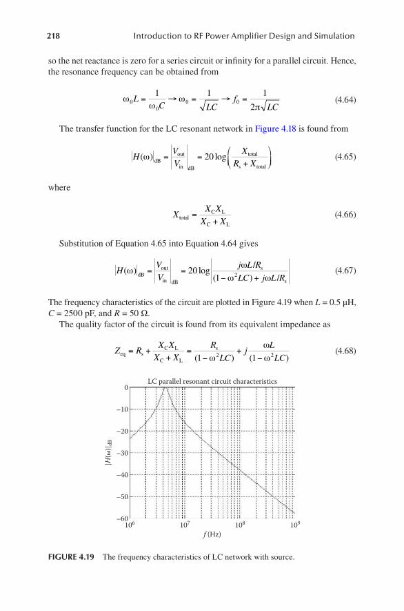
218 Introduction to RF Power Amplifier Design and Simulation
so the net reactance is zero for a series circuit or infinity for a parallel circuit. Hence, the resonance frequency can be obtained from
ωω
ωπ
00
0 01 1 1
2L
C LCf
LC= → = → = (4.64)
The transfer function for the LC resonant network in Figure 4.18 is found from
HVV
XR X
( ) logω dBout
in dB
total
s total
= =+
20 (4.65)
where
XX XX Xtotal
C L
C L
=+
(4.66)
Substitution of Equation 4.65 into Equation 4.64 gives
HVV
j L R
LC j L R( ) log
( )ω
ω
ω ωdBout
in dB
s
s
/
/= =
− +20
1 2 (4.67)
The frequency characteristics of the circuit are plotted in Figure 4.19 when L = 0.5 μH, C = 2500 pF, and R = 50 Ω.
The quality factor of the circuit is found from its equivalent impedance as
Z RX XX X
R
LCj
L
LCeq s
C L
C L
s= ++
=−
+−( ) ( )1 12 2ω
ω
ω (4.68)
0
–10
–20
–30
–40
–50
–60106 107 108
f (Hz)
LC parallel resonant circuit characteristics
|H(ω
)| dB
109
FIGURE 4.19 The frequency characteristics of LC network with source.
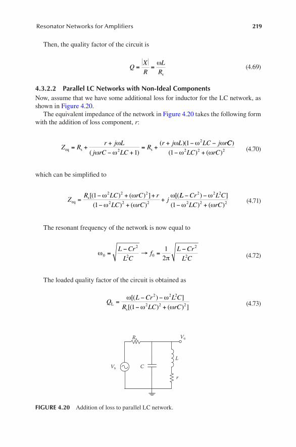
219Resonator Networks for Amplifiers
Then, the quality factor of the circuit is
QXR
LR
= =ω
s
(4.69)
4.3.2.2 Parallel LC Networks with Non-Ideal ComponentsNow, assume that we have some additional loss for inductor for the LC network, as shown in Figure 4.20.
The equivalent impedance of the network in Figure 4.20 takes the following form with the addition of loss component, r:
Z Rr j L
j rC LCR
r j L LC j req s s= +
+
− += +
+ − −ω
ω ω
ω ω ω
( )
( )(2
2
1
1 CC
LC rC
)
( ) ( )1 2 2 2− +ω ω (4.70)
which can be simplified to
ZR LC rC r
LC rCjeq
s=− + +
− ++
[( ) ( ) ]
( ) ( )
[(1
1
2 2 2
2 2 2
ω ω
ω ω
ω LL Cr L C
LC rC
− −
− +
2 2 2
2 2 21
) ]
( ) ( )
ω
ω ω (4.71)
The resonant frequency of the network is now equal to
ωπ0
2
2 0
2
2
12
=−
→ =−L Cr
L Cf
L Cr
L C (4.72)
The loaded quality factor of the circuit is obtained as
QL Cr L C
R LC rCL
s
=− −
− +
ω ω
ω ω
[( ) ]
[( ) ( ) ]
2 2 2
2 2 21 (4.73)
Rs
CL
Vs
Vo
r
FIGURE 4.20 Addition of loss to parallel LC network.
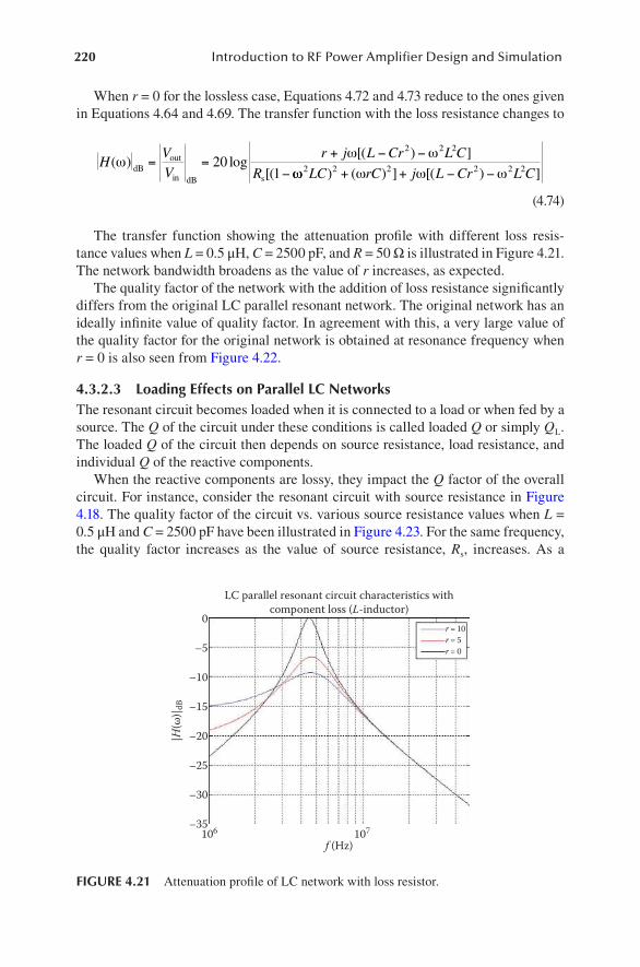
220 Introduction to RF Power Amplifier Design and Simulation
When r = 0 for the lossless case, Equations 4.72 and 4.73 reduce to the ones given in Equations 4.64 and 4.69. The transfer function with the loss resistance changes to
HVV
r j L Cr L C
R( ) log
[( ) ]
[(ω
ω ωdB
out
in dB s
= =+ − −
−20
1
2 2 2
ωω ω ω ω2 2 2 2 2 2LC rC j L Cr L C) ( ) ] [( ) ]+ + − −
(4.74)
The transfer function showing the attenuation profile with different loss resis-tance values when L = 0.5 μH, C = 2500 pF, and R = 50 Ω is illustrated in Figure 4.21. The network bandwidth broadens as the value of r increases, as expected.
The quality factor of the network with the addition of loss resistance significantly differs from the original LC parallel resonant network. The original network has an ideally infinite value of quality factor. In agreement with this, a very large value of the quality factor for the original network is obtained at resonance frequency when r = 0 is also seen from Figure 4.22.
4.3.2.3 Loading Effects on Parallel LC NetworksThe resonant circuit becomes loaded when it is connected to a load or when fed by a source. The Q of the circuit under these conditions is called loaded Q or simply QL. The loaded Q of the circuit then depends on source resistance, load resistance, and individual Q of the reactive components.
When the reactive components are lossy, they impact the Q factor of the overall circuit. For instance, consider the resonant circuit with source resistance in Figure 4.18. The quality factor of the circuit vs. various source resistance values when L = 0.5 μH and C = 2500 pF have been illustrated in Figure 4.23. For the same frequency, the quality factor increases as the value of source resistance, Rs, increases. As a
0r = 10r = 5r = 0–5
–10
–15
–20
–25
–30
–35106 107
f (Hz)
LC parallel resonant circuit characteristics withcomponent loss (L-inductor)
|H(ω
)| dB
FIGURE 4.21 Attenuation profile of LC network with loss resistor.
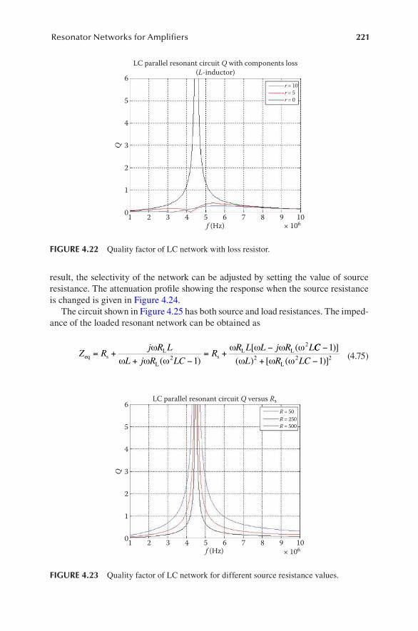
221Resonator Networks for Amplifiers
result, the selectivity of the network can be adjusted by setting the value of source resistance. The attenuation profile showing the response when the source resistance is changed is given in Figure 4.24.
The circuit shown in Figure 4.25 has both source and load resistances. The imped-ance of the loaded resonant network can be obtained as
Z Rj R L
L j R LCR
R L L j R Leq s
L
Ls
L L= ++ −
= +−ω
ω ω ω
ω ω ω ω
( )
[ (2
2
1
CC
L R LC
−
+ −
1
12 2 2
)]
( ) [ ( )]ω ω ωL (4.75)
6r = 10r = 5r = 05
4
3
2
1
01 2 3 4 5 6f (Hz)
LC parallel resonant circuit Q with components loss(L-inductor)
Q
× 1067 8 9 10
FIGURE 4.22 Quality factor of LC network with loss resistor.
6
5
4
3
2
1
01 2 3
Q
4 5 6f (Hz)
LC parallel resonant circuit Q versus Rs
R = 50R = 250R = 500
× 1067 8 9 10
FIGURE 4.23 Quality factor of LC network for different source resistance values.
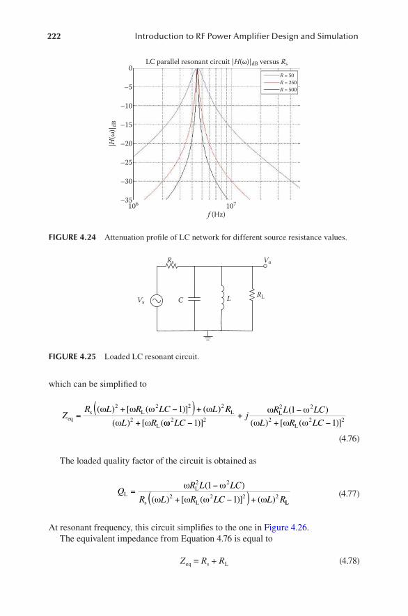
222 Introduction to RF Power Amplifier Design and Simulation
which can be simplified to
Z
R L R LC L R
L Req
s L L
L
=+ −( ) +
+
( ) [ ( )] ( )
( ) [ (
ω ω ω ω
ω ω
2 2 2 2
2
1
ωω
ω ω
ω ω ω2 2
2 2
2 2 21
1
1LCj
R L LC
L R LC−+
−
+ −)]
( )
( ) [ ( )]L
L (4.76)
The loaded quality factor of the circuit is obtained as
QR L LC
R L R LC L RL
L
s L
=−
+ −( ) +ω ω
ω ω ω ω
2 2
2 2 2 2
1
1
( )
( ) [ ( )] ( ) LL (4.77)
At resonant frequency, this circuit simplifies to the one in Figure 4.26.The equivalent impedance from Equation 4.76 is equal to
Zeq = Rs + RL (4.78)
0
–5
–10
–15
–20
–25
–30
–35106 107
f (Hz)
LC parallel resonant circuit |H(ω)|dB versus Rs
R = 50R = 250R = 500
|H(ω
)| dB
FIGURE 4.24 Attenuation profile of LC network for different source resistance values.
Rs
C LVs
Vo
RL
FIGURE 4.25 Loaded LC resonant circuit.
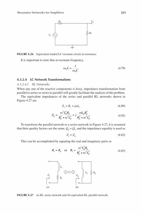
223Resonator Networks for Amplifiers
It is important to note that at resonant frequency,
ωω0
0
1L
C= (4.79)
4.3.2.4 LC Network Transformations4.3.2.4.1 RL NetworksWhen any one of the reactive components is lossy, impedance transformation from parallel to series or series to parallel will greatly facilitate the analysis of the problem.
The equivalent impedances of the series and parallel RL networks shown in Figure 4.27 are
Zs = Rs + jωLs (4.80)
ZL R
R Lj
L R
R Lp
p p
p p
p p
p p
=+
++
ω
ω
ω
ω
2 2
2 2 2
2
2 2 2 (4.81)
To transform the parallel network to a series network in Figure 4.27, it is assumed that their quality factors are the same, Qp = Qs, and the impedance equality is used as
Zs = Zp (4.82)
This can be accomplished by equating the real and imaginary parts as
R R RL R
R Ls p s
p p
p p
or= =+
ω
ω
2 2
2 2 2 (4.83)
Rs
Vs
Vo
RL
FIGURE 4.26 Equivalent loaded LC resonant circuit at resonance.
Ls
Rs
Lp RpZs Zp
(a) (b)
FIGURE 4.27 (a) RL series network and (b) equivalent RL parallel network.
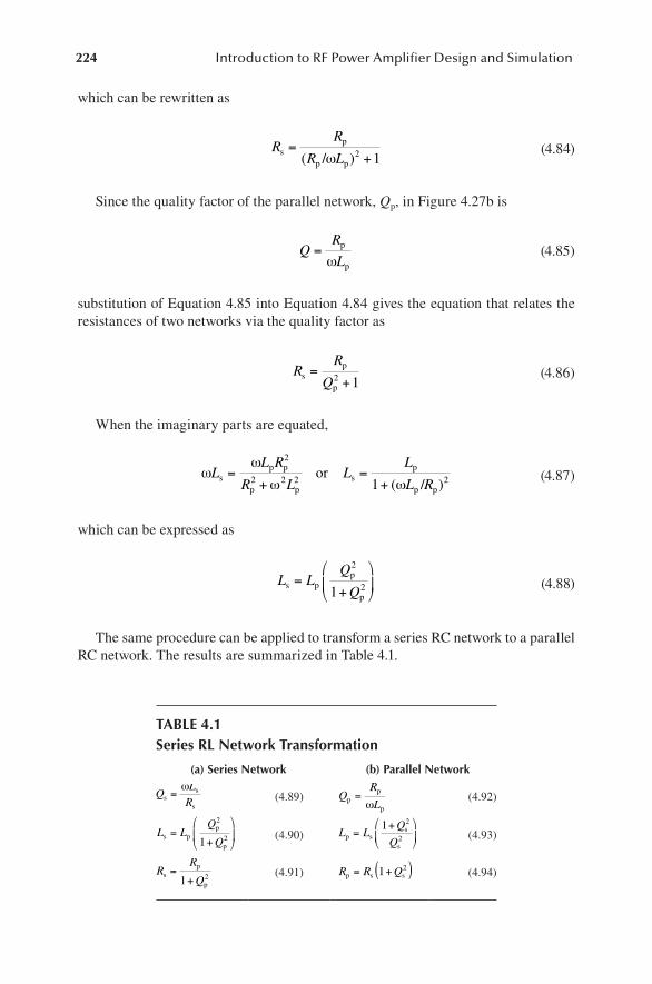
224 Introduction to RF Power Amplifier Design and Simulation
which can be rewritten as
RR
R Ls
p
p p/=
+( )ω 2 1 (4.84)
Since the quality factor of the parallel network, Qp, in Figure 4.27b is
QR
L= p
pω (4.85)
substitution of Equation 4.85 into Equation 4.84 gives the equation that relates the resistances of two networks via the quality factor as
RR
Qs
p
p
=+2 1
(4.86)
When the imaginary parts are equated,
ωω
ω ωL
L R
R LL
L
L Rs
p p
p ps
p
p p
or/
=+
=+
2
2 2 2 21 ( ) (4.87)
which can be expressed as
L LQ
Qs p
p
p
=+
2
21 (4.88)
The same procedure can be applied to transform a series RC network to a parallel RC network. The results are summarized in Table 4.1.
TABLE 4.1Series RL Network Transformation
(a) Series Network (b) Parallel Network
QLRs
s
s
=ω
(4.89) QR
Lpp
p
=ω
(4.92)
L LQ
Qs p
p
p
=+
2
21(4.90) L L
Q
Qp s
s
s
=+1 2
2 (4.93)
RR
Qs
p
p
=+1 2 (4.91) R R Qp s s= +( )1 2 (4.94)
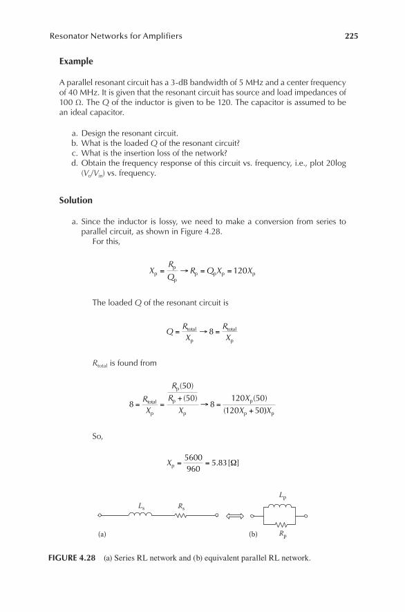
225Resonator Networks for Amplifiers
Example
A parallel resonant circuit has a 3-dB bandwidth of 5 MHz and a center frequency of 40 MHz. It is given that the resonant circuit has source and load impedances of 100 Ω. The Q of the inductor is given to be 120. The capacitor is assumed to be an ideal capacitor.
a. Design the resonant circuit. b. What is the loaded Q of the resonant circuit? c. What is the insertion loss of the network? d. Obtain the frequency response of this circuit vs. frequency, i.e., plot 20log
(Vo/Vin) vs. frequency.
Solution
a. Since the inductor is lossy, we need to make a conversion from series to parallel circuit, as shown in Figure 4.28.
For this,
XR
QR Q X Xp
p
pp p p p= → = =120
The loaded Q of the resonant circuit is
QRX
RX
= → =total
p
total
p
8
Rtotal is found from
8 total
p
p
p
p
p
p
= =+
→ =+
RX
R
R
X
X
X
( )
( ) ( )
(
50
508
120 50
120 50))Xp
So,
Xp = =5600960
5 83. [ ]Ω
Ls Rs
Lp
Rp(a) (b)
FIGURE 4.28 (a) Series RL network and (b) equivalent parallel RL network.
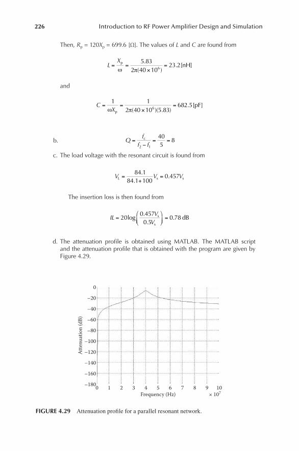
226 Introduction to RF Power Amplifier Design and Simulation
Then, Rp = 120Xp = 699.6 [Ω]. The values of L and C are found from
LX
= =×
=p
ω π
5 832 40 10
23 26
.( )
. [ ]nH
and
CX
= =×
=1 1
2 40 10 5 83682 56ω πp
pF( )( . )
. [ ]
b. Q
ff f
=−
= =c
2 1
405
8
c. The load voltage with the resonant circuit is found from
V V VL s s=+
=84 1
84 1 1000 457
..
.
The insertion loss is then found from
ILVV
= =200 4570 5
0 78log..
.s
s
dB
d. The attenuation profile is obtained using MATLAB. The MATLAB script and the attenuation profile that is obtained with the program are given by Figure 4.29.
0
–20
–40
–60
–80
–100
–120
–140
–160
–1800 1 2 3 4 5Frequency (Hz) × 107
Atte
nuat
ion
(dB)
6 7 8 9 10
FIGURE 4.29 Attenuation profile for a parallel resonant network.

227Resonator Networks for Amplifiers
clearf = linspace(1,100*10^6);RL = 100;RS = 100;RP = 699.6;Q = 12;XP = 5.83;fc = 40*10^6;wc = 2*pi()*fc;L = XP/(wc);C = 1/(wc*XP);
w = 2*pi.*f;XL=1j.*w.*L;XC=-1j./(w.*C);Xeq=(XL.*XC)./(XL+XC);Req=(RP*RL)./(RP+RL);Zeq=(Req.*Xeq)./(Req+Xeq);S21=20.*log10(abs(Zeq./(Zeq+RS)));
plot(f,S21);
grid ontitle('Attenuation Profile')xlabel('Frequency (Hz)')ylabel('Attenuation (dB)')
4.3.2.4.2 RC NetworksConsider the RC parallel circuits shown in Figure 4.30. To transform the parallel RC network to a series RC network so that both circuits would have the same quality fac-tors, the same approach in Section 4.3.2.4.1 is used, and the impedances are equated as
Zs = Zp (4.95)
where
ZR
R C
R C
R Cp
p
p p
p p
p p
=+
−+1 12
2
2( ) ( )ω
ω
ω (4.96)
Z RjCs s
s
= −ω
(4.97)
Equating the real and imaginary parts gives
RR
R C
R
Qs
p
p p
p
p
=+
=+1 12 2( )ω
(4.98)
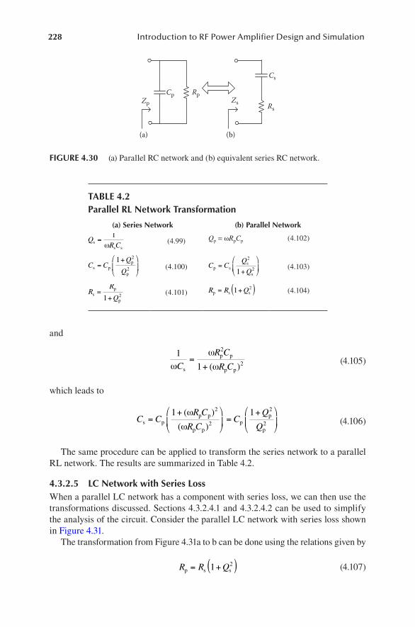
228 Introduction to RF Power Amplifier Design and Simulation
and
1
1
2
2ω
ω
ωC
R C
R Cs
p p
p p
=+ ( )
(4.105)
which leads to
C CR C
R CC
Q
Qs p
p p
p pp
p
p
=+
=
+
1 12
2
2
2
( )
( )
ω
ω (4.106)
The same procedure can be applied to transform the series network to a parallel RL network. The results are summarized in Table 4.2.
4.3.2.5 LC Network with Series LossWhen a parallel LC network has a component with series loss, we can then use the transformations discussed. Sections 4.3.2.4.1 and 4.3.2.4.2 can be used to simplify the analysis of the circuit. Consider the parallel LC network with series loss shown in Figure 4.31.
The transformation from Figure 4.31a to b can be done using the relations given by
R R Qp s s= +( )1 2 (4.107)
Cs
RsZs
CpZp
Rp
(a) (b)
FIGURE 4.30 (a) Parallel RC network and (b) equivalent series RC network.
TABLE 4.2Parallel RL Network Transformation
(a) Series Network (b) Parallel Network
QR Css s
=1
ω (4.99) Qp = ωRpCp (4.102)
C CQ
Qs p
p
p
=+1 2
2 (4.100) C CQ
Qp s
s
s
=+
2
21(4.103)
RR
Qs
p
p
=+1 2 (4.101) R R Qp s s= +( )1 2 (4.104)
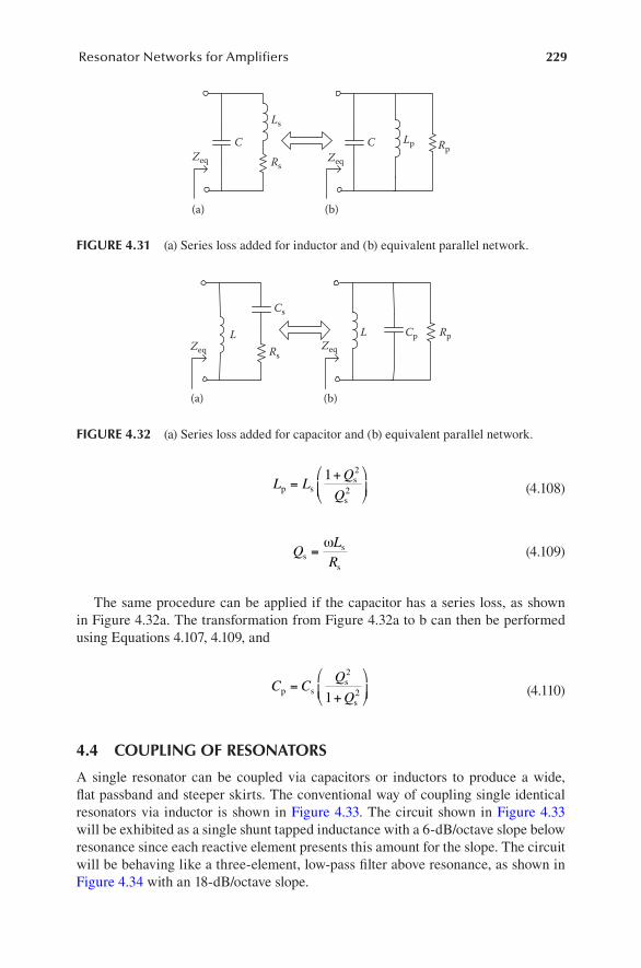
229Resonator Networks for Amplifiers
L LQ
Qp s
s
s
=+1 2
2 (4.108)
QLRs
s
s
=ω
(4.109)
The same procedure can be applied if the capacitor has a series loss, as shown in Figure 4.32a. The transformation from Figure 4.32a to b can then be performed using Equations 4.107, 4.109, and
C CQ
Qp s
s
s
=+
2
21 (4.110)
4.4 COUPLING OF RESONATORS
A single resonator can be coupled via capacitors or inductors to produce a wide, flat passband and steeper skirts. The conventional way of coupling single identical resonators via inductor is shown in Figure 4.33. The circuit shown in Figure 4.33 will be exhibited as a single shunt tapped inductance with a 6-dB/octave slope below resonance since each reactive element presents this amount for the slope. The circuit will be behaving like a three-element, low-pass filter above resonance, as shown in Figure 4.34 with an 18-dB/octave slope.
CZeq Rs
Ls
CZeq
RpLp
(b)(a)
FIGURE 4.31 (a) Series loss added for inductor and (b) equivalent parallel network.
Cs
Zeq Rs
L CpZeq
RpL
(b)(a)
FIGURE 4.32 (a) Series loss added for capacitor and (b) equivalent parallel network.
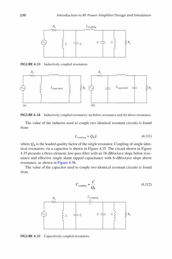
230 Introduction to RF Power Amplifier Design and Simulation
The value of the inductor used to couple two identical resonant circuits is found from
Lcoupling = QRL (4.111)
where QR is the loaded quality factor of the single resonator. Coupling of single iden-tical resonators via a capacitor is shown in Figure 4.35. The circuit shown in Figure 4.35 presents a three-element, low-pass filter with an 18-dB/octave slope below reso-nance and effective single shunt tapped capacitance with 6-dB/octave slope above resonance, as shown in Figure 4.36.
The value of the capacitor used to couple two identical resonant circuits is found from
CCQcoupling
R
= (4.112)
LcouplingRs
RLL C LC
FIGURE 4.33 Inductively coupled resonators.
Lequivalent
Rs
RL
Rs
RLCequivalent
(b)(a)
FIGURE 4.34 Inductively coupled resonators: (a) below resonance and (b) above resonance.
CcouplingRs
RLL C LC
FIGURE 4.35 Capacitively coupled resonators.
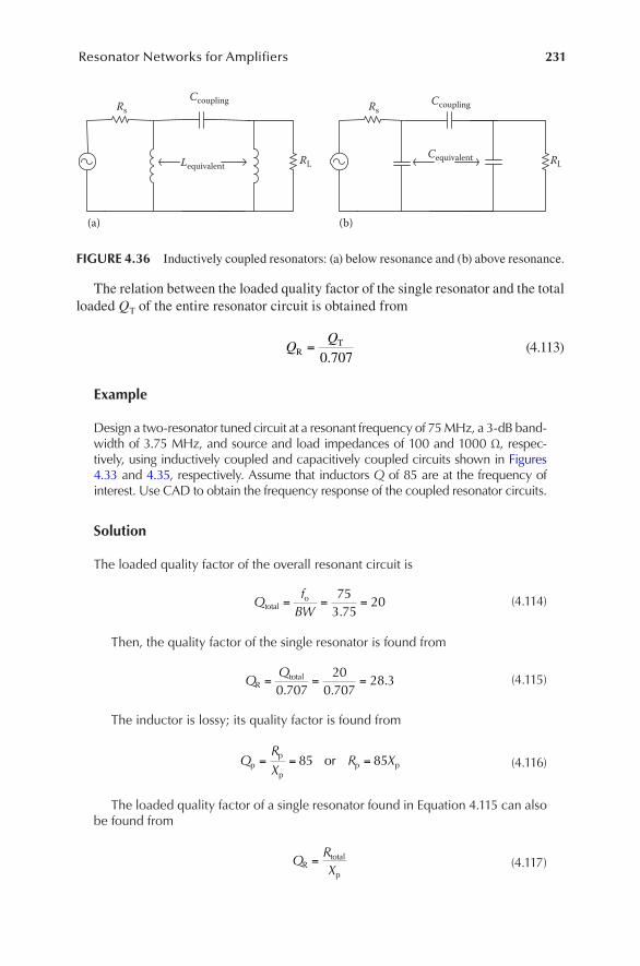
231Resonator Networks for Amplifiers
The relation between the loaded quality factor of the single resonator and the total loaded QT of the entire resonator circuit is obtained from
RT=
0 707. (4.113)
Example
Design a two-resonator tuned circuit at a resonant frequency of 75 MHz, a 3-dB band-width of 3.75 MHz, and source and load impedances of 100 and 1000 Ω, respec-tively, using inductively coupled and capacitively coupled circuits shown in Figures 4.33 and 4.35, respectively. Assume that inductors Q of 85 are at the frequency of interest. Use CAD to obtain the frequency response of the coupled resonator circuits.
Solution
The loaded quality factor of the overall resonant circuit is
QfBWtotal
o= = =753 75
20.
(4.114)
Then, the quality factor of the single resonator is found from
Rtotal= = =
0 70720
0 70728 3
. .. (4.115)
The inductor is lossy; its quality factor is found from
QR
XR Xp
p
pp por= = =85 85 (4.116)
The loaded quality factor of a single resonator found in Equation 4.115 can also be found from
QRXRtotal
p
= (4.117)
Lequivalent
Rs
RL
Rs
RLCequivalent
Ccoupling Ccoupling
(a) (b)
FIGURE 4.36 Inductively coupled resonators: (a) below resonance and (b) above resonance.
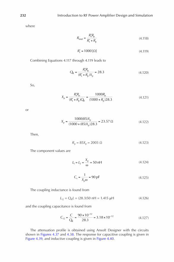
232 Introduction to RF Power Amplifier Design and Simulation
where
RR R
R Rtotals p
s p
=′
′ + (4.118)
′ =Rs 1000[ ]Ω (4.119)
Combining Equations 4.117 through 4.119 leads to
QRR
R R XRs p
s p p
=′
′ +=
( ).28 3 (4.120)
So,
XR R
R R Q
R
Rps p
s p R
p
p
=′
′ +=
+( ) ( ) .
1000
1000 28 3 (4.121)
or
XX
Xpp
p
=+
=1000 85
1000 85 28 323 57
( )
( ( ) ) .. Ω (4.122)
Then,
Rp = 85Xp = 2003 Ω (4.123)
The component values are
L LX
1 2 50= = =p nHω
(4.124)
CXsp
pF= =1
90ω
(4.125)
The coupling inductance is found from
L12 = QRL = (28.3)50 nH = 1.415 μH (4.126)
and the coupling capacitance is found from
CCQ12
121290 10
28 33 18 10= =
×= ×
−−
R .. (4.127)
The attenuation profile is obtained using Ansoft Designer with the circuits shown in Figures 4.37 and 4.38. The response for capacitive coupling is given in Figure 4.39, and inductive coupling is given in Figure 4.40.
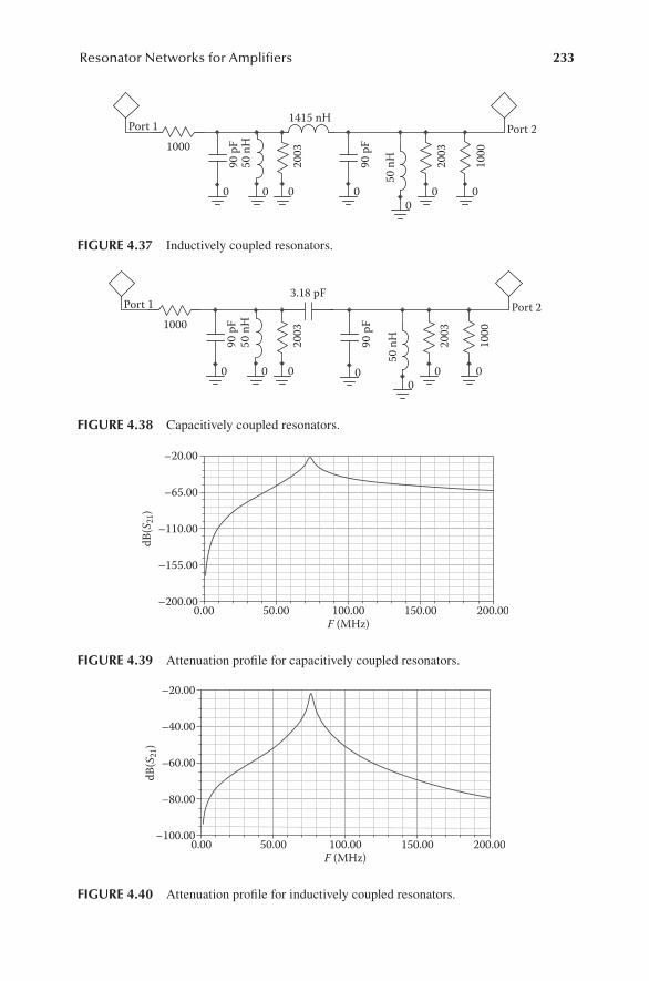
233Resonator Networks for Amplifiers
0 0 0 00
0 0
1000
90 p
F
90 p
F
50 n
H
50 n
H2003
2003
1000
Port 11415 nH
Port 2
FIGURE 4.37 Inductively coupled resonators.
0 0 0 00
0 0
1000
90 p
F
90 p
F
50 n
H
50 n
H2003
2003
1000
Port 13.18 pF
Port 2
FIGURE 4.38 Capacitively coupled resonators.
–20.00
–65.00
–110.00
–155.00
–200.000.00 50.00 100.00
F (MHz)
dB(S
21)
150.00 200.00
FIGURE 4.39 Attenuation profile for capacitively coupled resonators.
–20.00
–40.00
–60.00
–80.00
–100.000.00 50.00 100.00
F (MHz)
dB(S
21)
150.00 200.00
FIGURE 4.40 Attenuation profile for inductively coupled resonators.
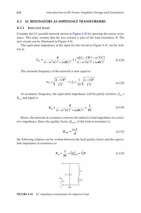
234 Introduction to RF Power Amplifier Design and Simulation
4.5 LC RESONATORS AS IMPEDANCE TRANSFORMERS
4.5.1 inductive load
Consider the LC parallel network shown in Figure 4.20 by ignoring the source resis-tance. This time, assume that the loss resistor is part of the load resistance, R. The new circuit can be illustrated in Figure 4.41.
The equivalent impedance at the input for the circuit in Figure 4.41 can be writ-ten as
ZR
LC RCj
L CR L C
LCeq =
− ++
− −
−( ) ( )
[( ) ]
( )1 12 2 2
2 2 2
2ω ω
ω ω
ω 22 2+ ( )ωRC (4.128)
The resonant frequency of the network is now equal to
ωπ0
2
2 0
2
2
12
=−
→ =−L CR
L Cf
L CR
L C (4.129)
At resonance frequency, the equivalent impedance will be purely resistive, Zeq = Req, and equal to
RR
LC RC
LRCeq =
− +=
( ) ( )1 2 2 2ω ω (4.130)
Hence, the network at resonance converts the inductive load impedance to a resis-tive impedance. Since the quality factor, Qload, of the load at resonance is
QLRload =
ω0 (4.131)
the following relation can be written between the load quality factor and the equiva-lent impedance at resonance as
RLRC
Q Req load= = +( )2 1 (4.132)
CL
RZeq
FIGURE 4.41 LC impedance transformer for inductive load.
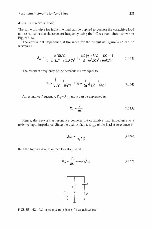
235Resonator Networks for Amplifiers
4.5.2 caPacitive load
The same principle for inductive load can be applied to convert the capacitive load to a resistive load at the resonant frequency using the LC resonant circuit shown in Figure 4.42.
The equivalent impedance at the input for the circuit in Figure 4.42 can be written as
ZRL C
LC RCjL R C LC
eq =− +
+− + ω
ω ω
ω ω4 2 2
2 2 2
2 2 2
1
1
( ) ( )
( ) − +( ) ( )1 2 2 2ω ωLC RC
(4.133)
The resonant frequency of the network is now equal to
ωπ0 2 2 0 2 2
1 12
1=
−→ =
−LC R Cf
LC R C (4.134)
At resonance frequency, Zeq = Req, and it can be expressed as
RLRCeq = (4.135)
Hence, the network at resonance converts the capacitive load impedance to a resistive input impedance. Since the quality factor, Qload, of the load at resonance is
QRCload =1
0ω (4.136)
then the following relation can be established:
RLRC
LQeq load= = ω0 (4.137)
CL
RZeq
FIGURE 4.42 LC impedance transformer for capacitive load.
236 Introduction to RF Power Amplifier Design and Simulation
Example
An amplifier output needs to be terminated with a load line resistance of 2000 Ω at 1.6 MHz. It is given in the data sheet that the transistor has 20 pF at 1.6 MHz. There is an inductive load connected to the output of the load line circuit of the amplifier with RL = 5 Ω. The configuration of this circuit is given in Figure 4.43.
a. Calculate the values of L and C by assuming that the load inductor has a negligible loss, i.e., r = 0.
b. The inductor is changed to a magnetic core inductor, which has the qual-ity factor of 50. Calculate the loss resistance, r, for the reactive component values obtained in (a). What is the value of new load line resistance?
c. If the quality factor is 50, the inductor is 50, and the load line resistor is required to be 2000 Ω as set in the problem, what are the values of L and C with RL = 5 Ω?
Solution
It is given that Req = 2000 Ω, RL = R = 5 Ω, Ctran = 20 pF, f = 1.6 MHz, ω0 = 107 rad/s, and CT = Ctran + C.
a. When r = 0 Ω, Equation 4.132 can be used as
R Q RR
RQ Qeq load
eqload load= +( ) → − = → =2 21 1 19 98. (4.138)
From Equation 4.131,
QL
RL
Q RLload
load= → = → =ω
ωµ0
0
10[ ]H (4.139)
Now, using Equation 4.130,
RL
RCC
LR R
CeqT
Teq
T= → = → =1[ ]nF (4.140)
Ctran
R
RL
L
C
r
FIGURE 4.43 Amplifier output load line circuit.
237Resonator Networks for Amplifiers
Since
CT = Ctran + C → C = CT − Ctran → C = 980 [pF] (4.141)
b. The Q of the inductor is given to be equal to 50. Then,
QLr
rL
Qrinductor
inductor
= → = → =ω ω0 0 2 [ ]Ω (4.142)
So, the new load resistance, Req, from Equation 4.120 is
RL
R r CeqT
=+
=×
×=
−
−( ) ( )( ). [ ]
10 107 1 10
1428 66
9Ω (4.143)
c. The Q of the inductor is given to be equal to 50. Then,
QLr
r L aLinductor = → = × =ω0 52 10 (4.144)
Since
R R Q R R r QL R aL
eq load eq load= +( )→ = + +( ) = + +2 2 02 2
1 1( )(ω ))2
R aL+ (4.145)
which leads to the solution for L as
L La R R
a
R R R
a2
02 2
02 2
20−
−
+−
−
+=
( ) ( )eq eq
ω ω (4.146)
From Equation 4.146, the inductance value is found as L = 12.2 [μH]. Substituting the value of L into Equation 4.144 gives the value of r as
r = 2 × 10⁵L = 2.44 [Ω]
where
L = 12.2 [μH]. (4.147)
Using Equation 4.140,
RL
RCC
LR R
CeqT
Teq
T= → = → = 820[ ]pF (4.148)
Since
CT = Ctran + C → C = 820 − 20 → C = 800 [pF] (4.149)
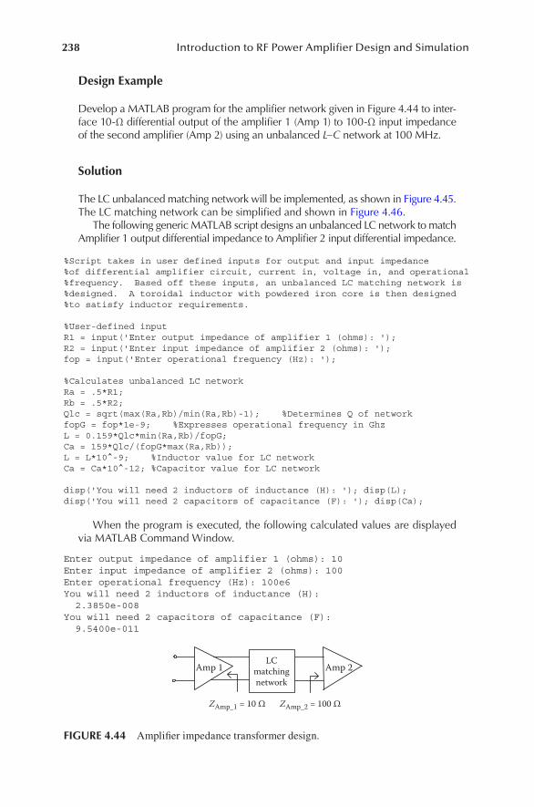
238 Introduction to RF Power Amplifier Design and Simulation
Design Example
Develop a MATLAB program for the amplifier network given in Figure 4.44 to inter-face 10-Ω differential output of the amplifier 1 (Amp 1) to 100-Ω input impedance of the second amplifier (Amp 2) using an unbalanced L–C network at 100 MHz.
Solution
The LC unbalanced matching network will be implemented, as shown in Figure 4.45. The LC matching network can be simplified and shown in Figure 4.46.
The following generic MATLAB script designs an unbalanced LC network to match Amplifier 1 output differential impedance to Amplifier 2 input differential impedance.
%Script takes in user defined inputs for output and input impedance%of differential amplifier circuit, current in, voltage in, and operational%frequency. Based off these inputs, an unbalanced LC matching network is %designed. A toroidal inductor with powdered iron core is then designed%to satisfy inductor requirements.
%User-defined inputR1 = input('Enter output impedance of amplifier 1 (ohms): ');R2 = input('Enter input impedance of amplifier 2 (ohms): ');fop = input('Enter operational frequency (Hz): ');
%Calculates unbalanced LC networkRa = .5*R1;Rb = .5*R2;Qlc = sqrt(max(Ra,Rb)/min(Ra,Rb)-1); %Determines Q of networkfopG = fop*1e-9; %Expresses operational frequency in GhzL = 0.159*Qlc*min(Ra,Rb)/fopG;Ca = 159*Qlc/(fopG*max(Ra,Rb));L = L*10^-9; %Inductor value for LC networkCa = Ca*10^-12; %Capacitor value for LC network
disp('You will need 2 inductors of inductance (H): '); disp(L);disp('You will need 2 capacitors of capacitance (F): '); disp(Ca);
When the program is executed, the following calculated values are displayed via MATLAB Command Window.
Enter output impedance of amplifier 1 (ohms): 10Enter input impedance of amplifier 2 (ohms): 100Enter operational frequency (Hz): 100e6You will need 2 inductors of inductance (H): 2.3850e-008You will need 2 capacitors of capacitance (F): 9.5400e-011
Amp 1 Amp 2LC
matchingnetwork
ZAmp_1 = 10 Ω ZAmp_2 = 100 Ω
FIGURE 4.44 Amplifier impedance transformer design.
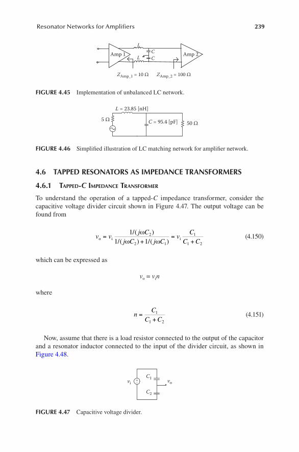
239Resonator Networks for Amplifiers
4.6 TAPPED RESONATORS AS IMPEDANCE TRANSFORMERS
4.6.1 taPPed-C imPedance transformer
To understand the operation of a tapped-C impedance transformer, consider the capacitive voltage divider circuit shown in Figure 4.47. The output voltage can be found from
v vj C
j C j Cv
CC Co i i
// /
=+
=+
11 1
2
2 1
1
1 2
( )( ) ( )
ωω ω
(4.150)
which can be expressed as
vo = vin
where
nC
C C=
+1
1 2
(4.151)
Now, assume that there is a load resistor connected to the output of the capacitor and a resonator inductor connected to the input of the divider circuit, as shown in Figure 4.48.
Amp 1 Amp 2L
LCC
ZAmp_1 = 10 Ω ZAmp_2 = 100 Ω
FIGURE 4.45 Implementation of unbalanced LC network.
5 Ω 50 Ω
L = 23.85 [nH]
C = 95.4 [pF]
FIGURE 4.46 Simplified illustration of LC matching network for amplifier network.
+–viC1
C2
vo
FIGURE 4.47 Capacitive voltage divider.
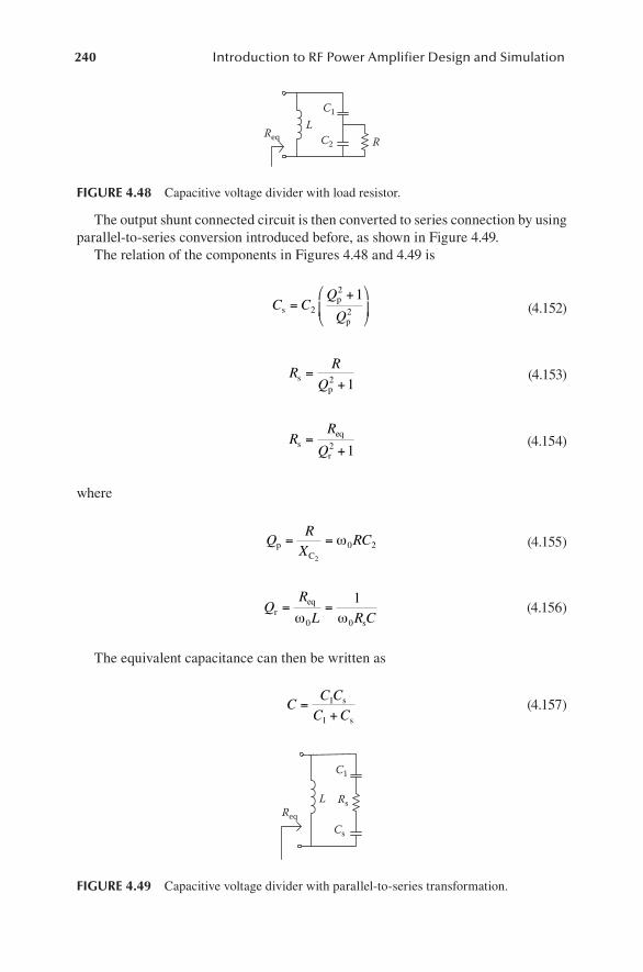
240 Introduction to RF Power Amplifier Design and Simulation
The output shunt connected circuit is then converted to series connection by using parallel-to-series conversion introduced before, as shown in Figure 4.49.
The relation of the components in Figures 4.48 and 4.49 is
C CQ
Qs
p
p
=+
2
2
2
1 (4.152)
RR
Qs
p
=+2 1
(4.153)
RR
Qs
eq
r
=+2 1
(4.154)
where
QRX
RCpC
= =2
0 2ω (4.155)
QR
L RCreq
s
= =ω ω0 0
1 (4.156)
The equivalent capacitance can then be written as
CC CC C
=+1
1
s
s
(4.157)
C1
C2 RL
Req
FIGURE 4.48 Capacitive voltage divider with load resistor.
C1
Cs
RsLReq
FIGURE 4.49 Capacitive voltage divider with parallel-to-series transformation.
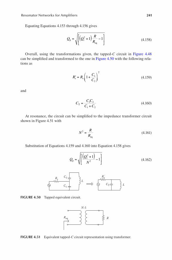
241Resonator Networks for Amplifiers
Equating Equations 4.153 through 4.156 gives
Q QRRp req
= +( ) −
2 1 1 (4.158)
Overall, using the transformations given, the tapped-C circuit in Figure 4.48 can be simplified and transformed to the one in Figure 4.50 with the following rela-tions as
′ = +
R R
CCs s 1 1
2
2
(4.159)
and
CC CC CT = +
1 2
1 2
(4.160)
At resonance, the circuit can be simplified to the impedance transformer circuit shown in Figure 4.51 with
NRR
2 =eq
(4.161)
Substitution of Equations 4.159 and 4.160 into Equation 4.158 gives
Np
r=+( )
−
2
2
11 (4.162)
C2
C1
LRs
Rs
CT L
FIGURE 4.50 Tapped equivalent circuit.
:1N
Req R
FIGURE 4.51 Equivalent tapped-C circuit representation using transformer.
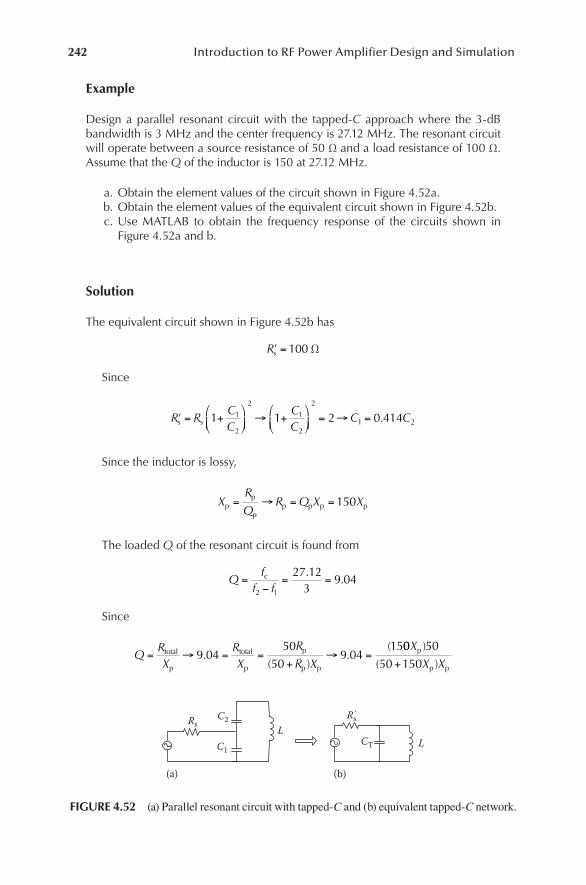
242 Introduction to RF Power Amplifier Design and Simulation
Example
Design a parallel resonant circuit with the tapped-C approach where the 3-dB bandwidth is 3 MHz and the center frequency is 27.12 MHz. The resonant circuit will operate between a source resistance of 50 Ω and a load resistance of 100 Ω. Assume that the Q of the inductor is 150 at 27.12 MHz.
a. Obtain the element values of the circuit shown in Figure 4.52a. b. Obtain the element values of the equivalent circuit shown in Figure 4.52b. c. Use MATLAB to obtain the frequency response of the circuits shown in
Figure 4.52a and b.
Solution
The equivalent circuit shown in Figure 4.52b has
′ =Rs 100Ω
Since
′ = +
→ +
= → =R R
CC
CC
C Cs s 1 1 2 0 4141
2
2
1
2
2
1 2.
Since the inductor is lossy,
XR
QR Q X Xp
p
pp p p p= → = =150
The loaded Q of the resonant circuit is found from
Qf
f f=
−= =c
2 1
27 123
9 04.
.
Since
QRX
RX
R
R X= → = =
+→ =total
p
total
p
p
p p
9.04 9.0450
50
15
( )
( 00 50
50 150
X
X Xp
p p
)
( )+
C2
C1
LRs
Rs
CT L
(a) (b)
FIGURE 4.52 (a) Parallel resonant circuit with tapped-C and (b) equivalent tapped-C network.

243Resonator Networks for Amplifiers
then
Xp = =70481356
5 2. [ ]Ω
So,
Rp = 150Xp = 780 [Ω]
The values of L and C are found from
LX
= =×
=p nHω π
5 22 27 12 10
30 56
.( . )
. [ ]
CXTp
pF= =×
=1 1
2 27 12 10 5 211286ω π( . )( . )
[ ]
The capacitor values for the circuit in Figure 4.52a are found from
CCCC C
CCT pF and=
+→ = → =1 2
1 2
221128
04141414
38526..
. [ ] CC1 1595= [ ]pF
The attenuation profile is obtained with the MATLAB script given below and plotted in Figure 4.53.
clearf = linspace(1,100*10^6);RL = 100;RS = 50;RP = 780;XP = 5.2;fc = 27.12*10^6;wc = 2*pi()*fc;L = XP/(wc);C = 1/(wc*XP); w = 2*pi.*f;XL=1j.*w.*L;XC=-1j./(w.*C);Xeq=(XL.*XC)./(XL+XC);Req=(RP*RL)./(RP+RL);Zeq=(Req.*Xeq)./(Req+Xeq);S21=20.*log10(abs(Zeq./(Zeq+RS))); plot(f,S21); grid ontitle('Attenuation Profile')xlabel('Frequency (Hz)')ylabel('Attenuation (dB)')
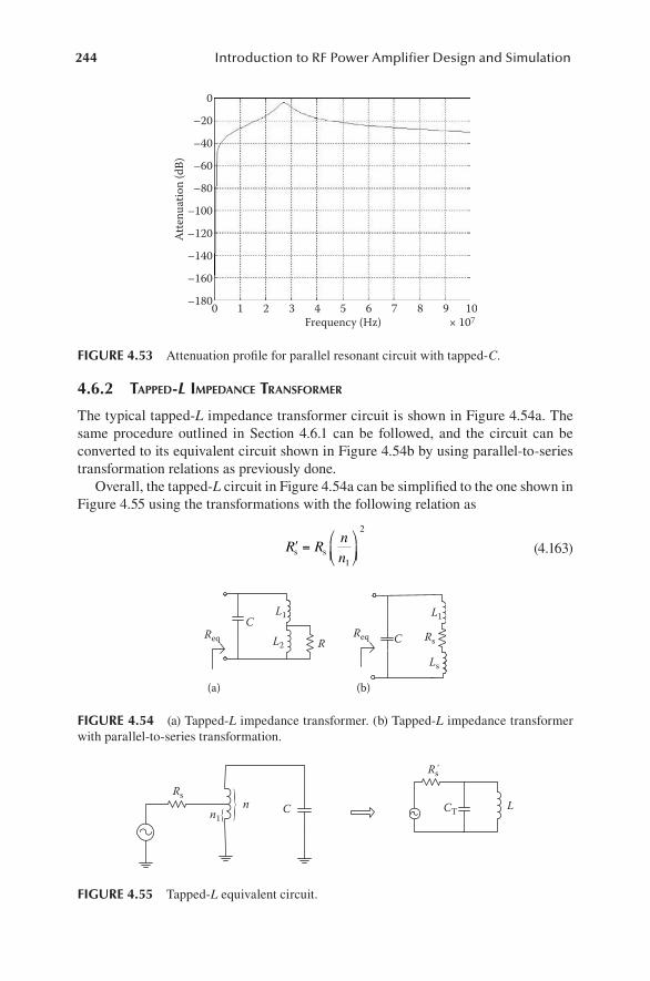
244 Introduction to RF Power Amplifier Design and Simulation
4.6.2 taPPed-L imPedance transformer
The typical tapped-L impedance transformer circuit is shown in Figure 4.54a. The same procedure outlined in Section 4.6.1 can be followed, and the circuit can be converted to its equivalent circuit shown in Figure 4.54b by using parallel-to-series transformation relations as previously done.
Overall, the tapped-L circuit in Figure 4.54a can be simplified to the one shown in Figure 4.55 using the transformations with the following relation as
′ =
R R
nns s1
2
(4.163)
0
–20
–40
–60
–80
–100
–120
–140
–160
–1800 1 2 3 4 5Frequency (Hz) × 107
Atte
nuat
ion
(dB)
6 7 8 9 10
FIGURE 4.53 Attenuation profile for parallel resonant circuit with tapped-C.
C
R
L1
Req L2 C
(a) (b)
L1
Req
Ls
Rs
FIGURE 4.54 (a) Tapped-L impedance transformer. (b) Tapped-L impedance transformer with parallel-to-series transformation.
nn1
RsC
Rs
CT L
FIGURE 4.55 Tapped-L equivalent circuit.
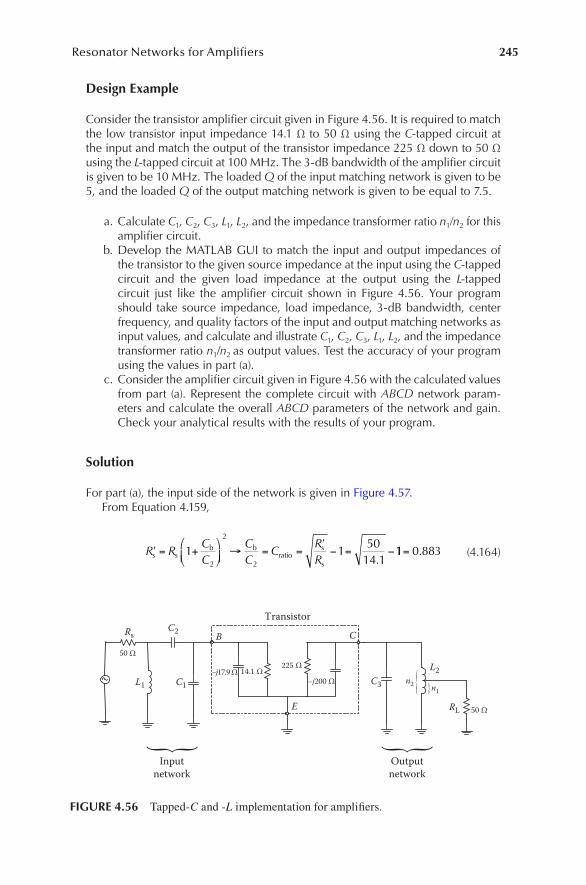
245Resonator Networks for Amplifiers
Design Example
Consider the transistor amplifier circuit given in Figure 4.56. It is required to match the low transistor input impedance 14.1 Ω to 50 Ω using the C-tapped circuit at the input and match the output of the transistor impedance 225 Ω down to 50 Ω using the L-tapped circuit at 100 MHz. The 3-dB bandwidth of the amplifier circuit is given to be 10 MHz. The loaded Q of the input matching network is given to be 5, and the loaded Q of the output matching network is given to be equal to 7.5.
a. Calculate C1, C2, C3, L1, L2, and the impedance transformer ratio n1/n2 for this amplifier circuit.
b. Develop the MATLAB GUI to match the input and output impedances of the transistor to the given source impedance at the input using the C-tapped circuit and the given load impedance at the output using the L-tapped circuit just like the amplifier circuit shown in Figure 4.56. Your program should take source impedance, load impedance, 3-dB bandwidth, center frequency, and quality factors of the input and output matching networks as input values, and calculate and illustrate C1, C2, C3, L1, L2, and the impedance transformer ratio n1/n2 as output values. Test the accuracy of your program using the values in part (a).
c. Consider the amplifier circuit given in Figure 4.56 with the calculated values from part (a). Represent the complete circuit with ABCD network param-eters and calculate the overall ABCD parameters of the network and gain. Check your analytical results with the results of your program.
Solution
For part (a), the input side of the network is given in Figure 4.57.From Equation 4.159,
′ = +
→ = =
′− = −R R
CC
CC
CRRs s
b bratio
s
s
1 15014 12
2
2 .11 0 883= . (4.164)
C2
C1 C3
RL
L2L1
Rs B C
E
Transistor
50 Ω
n1n2
Inputnetwork
Outputnetwork
50 Ω
14.1 Ω225 Ω
–j200 Ω–j17.9 Ω
FIGURE 4.56 Tapped-C and -L implementation for amplifiers.
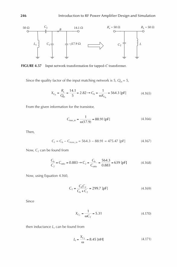
246 Introduction to RF Power Amplifier Design and Simulation
Since the quality factor of the input matching network is 5, Qin = 5,
XRQ
CXC
s
inb
Cb
b
pF= = = → = =14 15
2 821
564 3.
. . [ ]ω
(4.165)
From the given information for the transistor,
Ctran_in pF= =117 9
88 91ω( . )
. [ ] (4.166)
Then,
C1 = Cb − Ctrans_in = 564.3 − 88.91 = 475.47 [pF] (4.167)
Now, C2 can be found from
CC
C CCC
bratio
b
ratio
pF2
20 883564 30 883
639= = → = = =..
.[ ]] (4.168)
Now, using Equation 4.160,
CC CC CT
b
b
pF=+
=2
2
299 7. [ ] (4.169)
Since
XCC
TT= =
15 31
ω. (4.170)
then inductance L1 can be found from
LX
1 8 45= =CT nHω
. [ ] (4.171)
C2
C1 CTL1
B
L
RL = 50 ΩRs = 50 Ω50 Ω 14.1 Ω
–j17.9 Ω
FIGURE 4.57 Input network transformation for tapped-C transformer.
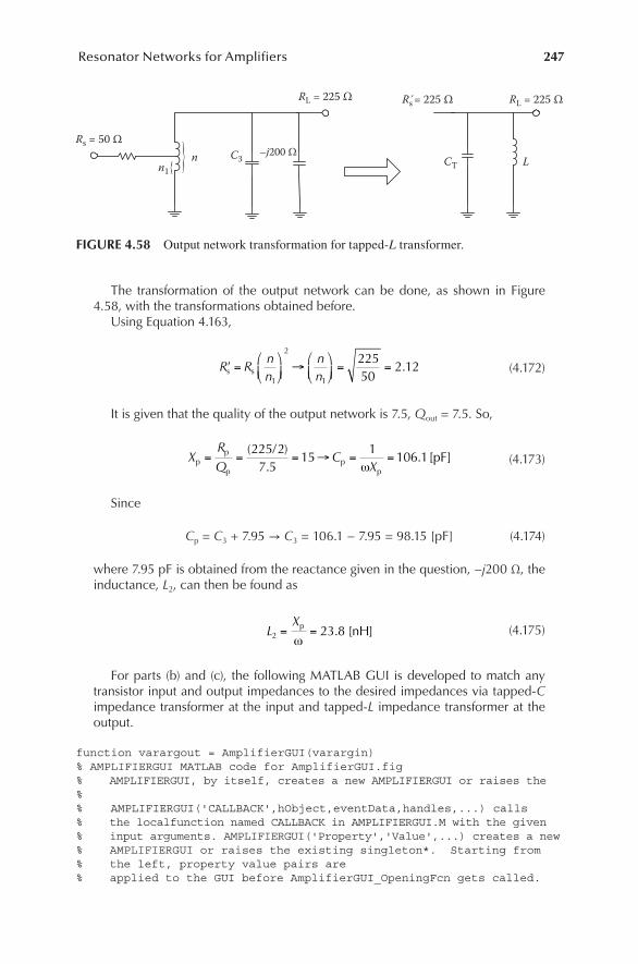
247Resonator Networks for Amplifiers
The transformation of the output network can be done, as shown in Figure 4.58, with the transformations obtained before.
Using Equation 4.163,
′ =
→
= =R R
nn
nns s
1
2
1
22550
2 12. (4.172)
It is given that the quality of the output network is 7.5, Qout = 7.5. So,
XR
QC
Xpp
pp
p
/pF= = = → = =
( ).
. [ ]225 27 5
151
106 1ω
(4.173)
Since
Cp = C3 + 7.95 → C3 = 106.1 − 7.95 = 98.15 [pF] (4.174)
where 7.95 pF is obtained from the reactance given in the question, −j200 Ω, the inductance, L2, can then be found as
LX
2 23 8= =p nHω
. [ ] (4.175)
For parts (b) and (c), the following MATLAB GUI is developed to match any transistor input and output impedances to the desired impedances via tapped-C impedance transformer at the input and tapped-L impedance transformer at the output.
function varargout = AmplifierGUI(varargin)% AMPLIFIERGUI MATLAB code for AmplifierGUI.fig% AMPLIFIERGUI, by itself, creates a new AMPLIFIERGUI or raises the %% AMPLIFIERGUI('CALLBACK',hObject,eventData,handles,...) calls% the localfunction named CALLBACK in AMPLIFIERGUI.M with the given% input arguments. AMPLIFIERGUI('Property','Value',...) creates a new% AMPLIFIERGUI or raises the existing singleton*. Starting from% the left, property value pairs are% applied to the GUI before AmplifierGUI_OpeningFcn gets called.
nn1
C3 CT L
RL = 225 Ω
Rs = 50 Ω
Rs = 225 Ω RL = 225 Ω
–j200 Ω
FIGURE 4.58 Output network transformation for tapped-L transformer.

248 Introduction to RF Power Amplifier Design and Simulation
% Begin initialization code - DO NOT EDITgui_Singleton = 1;gui_State = struct('gui_Name', mfilename, ... 'gui_Singleton', gui_Singleton, ... 'gui_OpeningFcn', @AmplifierGUI_OpeningFcn, ... 'gui_OutputFcn', @AmplifierGUI_OutputFcn, ... 'gui_LayoutFcn', [] , ... 'gui_Callback', []);if nargin && ischar(varargin1) gui_State.gui_Callback = str2func(varargin1);end if nargout [varargout1:nargout] = gui_mainfcn(gui_State, varargin:);else gui_mainfcn(gui_State, varargin:);end% End initialization code - DO NOT EDIT % --- Executes just before AmplifierGUI is made visible.function AmplifierGUI_OpeningFcn(hObject, eventdata, handles, varargin)
% hObject handle to figure% eventdata reserved - to be defined in a future version of MATLAB% handles structure with handles and user data (see GUIDATA)% varargin command line arguments to AmplifierGUI (see VARARGIN) % Choose default command line output for AmplifierGUIhandles.output = hObject; % Update handles structureguidata(hObject, handles); % UIWAIT makes AmplifierGUI wait for user response (see UIRESUME)% uiwait(handles.figure1); % --- Outputs from this function are returned to the command line.function varargout = AmplifierGUI_OutputFcn(hObject, eventdata, handles) % varargout cell array for returning output args (see VARARGOUT);% hObject handle to figure% eventdata reserved - to be defined in a future version of MATLAB% handles structure with handles and user data (see GUIDATA)
% Get default command line output from handles structurevarargout1 = handles.output;% --- Executes on button press in pushbutton1.function pushbutton1_Callback(hObject, eventdata, handles)% hObject handle to pushbutton1 (see GCBO)% eventdata reserved - to be defined in a future version of MATLAB% handles structure with handles and user data (see GUIDATA)Qin=str2num(get(handles.Qin,'String'));Qout=str2num(get(handles.Qout,'String'));RT1=str2num(get(handles.RT1,'String'));TR2=str2num(get(handles.TR2,'String'));
249Resonator Networks for Amplifiers
TC1=str2double(get(handles.TC1,'String'));TC2=str2double(get(handles.TC2,'String'));Cw=str2num(get(handles.Cw,'String'));w=str2num(get(handles.w,'String'));Rsource=str2double(get(handles.Rsource,'String'));Rload=str2num(get(handles.Rload,'String'));Qp=w/Cw;C1P=Qin/(2*pi*w*RT1);set(handles.C1p,'String',C1P);XTC1=1/(2*pi*w*1i*TC1);c1=C1P-XTC1;set(handles.C1,'String',c1);c2=C1P/(sqrt(Rsource/RT1)-1);set(handles.C2,'String',c2);Ceq=(C1P*c2)/(C1P+c2);Xp=1/(2*pi*w*Ceq);L1=Xp/(2*pi*w);set(handles.L1,'String',L1);XCT2=1/(2*pi*w*1i*TC2);N=sqrt(TR2/Rload);set(handles.N,'String',N);LRin=(Rload*(Qp*Qp+1))/(Qout*Qout+1);C3p=Qp/(2*pi*w*LRin);
set(handles.C3p,'String',C3p);C3=C3p-XCT2;set(handles.C3,'String',C3);L21=Rload/(2*pi*w*Qout);L22=(L21*(Qp*Qout-(Qout*Qout)))/((Qout*Qout)+1);L2=L22+L21;set(handles.L2,'String',L2);set(handles.L21,'String',L21);set(handles.L22,'String',L22);A_1=1;B_1=Rsource;C_1=0;D_1=1;ABCD_1=[A_1 B_1;C_1 D_1];YC1=1/(2*pi*w*c1*1i);YC11=1/YC1;YC2=1/(2*pi*w*c2*1i);YC22=1/YC2;YL1=(1i*L1*2*pi*w);YL11=1/YL1;A_2=1+(YC22/YC11);B_2=1/YC11;C_2=YL11+YC22+((YL11*YC22)/YC11);D_2=1+(YL11/YC11);ABCD_2=[A_2 B_2;C_2 D_2];ABCDtotal_1=ABCD_1*ABCD_2;set(handles.CA,'String',[real(ABCDtotal_1(1,1)), imag(ABCDtotal_1(1,1))].');set(handles.CB,'String',[real(ABCDtotal_1(1,2)), imag(ABCDtotal_1(1,2))].');set(handles.CC,'String',[real(ABCDtotal_1(2,1)), imag(ABCDtotal_1(2,1))].');set(handles.CD,'String',[real(ABCDtotal_1(2,2)), imag(ABCDtotal_1(2,2))].');TY11=str2double(get(handles.edit4,'String'));TY12=str2double(get(handles.edit5,'String'));
250 Introduction to RF Power Amplifier Design and Simulation
TY21=str2double(get(handles.edit6,'String'));TY22=str2double(get(handles.edit7,'String'));Ytrans=(1/1000).*[TY11 TY12; TY21 TY22];Ydet=det(Ytrans);ABCDtrans=[-Ytrans(2,2)/Ytrans(2,1) -1./Ytrans(2,1);-Ydet/Ytrans(2,1) -Ytrans(1,1)/Ytrans(2,1)];set(handles.TA,'String',[real(ABCDtrans(1,1)), imag(ABCDtrans(1,1))].');set(handles.TB,'String',[real(ABCDtrans(1,2)), imag(ABCDtrans(1,2))].');set(handles.TC,'String',[real(ABCDtrans(2,1)), imag(ABCDtrans(2,1))].');set(handles.TD,'String',[real(ABCDtrans(2,2)), imag(ABCDtrans(2,2))].');ImpC3=1/(2*pi*w*C3*1i);YL1=(2*pi*w*L22*1i);YL2=(2*pi*w*L21*1i);Series=((Rload*YL2)/(Rload+YL2))+YL1;Outputsimple=(Series*ImpC3)/((Series+ImpC3));A=1;B=0;C=1./Outputsimple;D=1;ABCDOutput=[A B;C D];set(handles.LA,'String',[real(ABCDOutput(1,1)), imag(ABCDOutput(1,1))].');set(handles.LB,'String',[real(ABCDOutput(1,2)), imag(ABCDOutput(1,2))].');set(handles.LC,'String',[real(ABCDOutput(2,1)), imag(ABCDOutput(2,1))].');set(handles.LD,'String',[real(ABCDOutput(2,2)), imag(ABCDOutput(2,2))].');ABCD=ABCDtotal_1*ABCDtrans*ABCDOutput;set(handles.A,'String',[real(ABCD(1,1)), imag(ABCD(1,1))].');set(handles.B,'String',[real(ABCD(1,2)), imag(ABCD(1,2))].');set(handles.C,'String',[real(ABCD(2,1)), imag(ABCD(2,1))].');set(handles.D,'String',[real(ABCD(2,2)), imag(ABCD(2,2))].');Vg=20*log10(abs(1/ABCD(1,1)));set(handles.Vg,'String',Vg);%Frequency Response Plotting over range of Frequencies.range=[1:100000:2*w];n=1;V=length(range);for n=(1:1:V)freq=n*100000;Qp=freq/(Cw);A_1=1;B_1=Rsource;C_1=0;D_1=1;ABCD_1=[A_1 B_1;C_1 D_1];YC1=1/(2*pi*freq*c1*1i);YC11=1/YC1;YC2=1/(2*pi*freq*c2*1i);YC22=1/YC2;YL1=(1i*L1*2*pi*freq);YL11=1/YL1;A_2=1+(YC22/YC11);B_2=1/YC11;C_2=YL11+YC22+((YL11*YC22)/YC11);D_2=1+(YL11/YC11);ABCD_2=[A_2 B_2;C_2 D_2];ABCDtotal_1=ABCD_1*ABCD_2;Ytrans=(1/1000).*[TY11 TY12; TY21 TY22];Ydet=det(Ytrans);
251Resonator Networks for Amplifiers
ABC Dtrans=[-Ytrans(2,2)/Ytrans(2,1) -1./Ytrans(2,1);-Ydet/Ytrans(2,1) -Ytrans(1,1)/Ytrans(2,1)];
ImpC3=1/(2*pi*freq*C3*1i);YL1=(2*pi*freq*L22*1i);YL2=(2*pi*freq*L21*1i);Series=((Rload*YL2)/(Rload+YL2))+YL1;Outputsimple=(Series*ImpC3)/((Series+ImpC3));A=1;B=0;C=1./Outputsimple;D=1;ABCDOutput=[A B;C D];ABCD=ABCDtotal_1*ABCDtrans*ABCDOutput;gain=1/(ABCD(1,1));VG(n)= 20*log10(abs(gain)); endVG;plot(range,VG);title('Frequency Response');xlabel('Frequency (Hz)');ylabel('Gain (dB)');
The last section of the program is not included due to its standard format for GUIs. When the program is executed, the MATLAB GUI window showing the results appears and is illustrated in Figure 4.59.
Design Example
Consider the capacitively coupled amplifier circuit shown in Figure 4.60. Design the resonator-tuned amplifier circuit at a resonant frequency of 100 MHz, 3-dB bandwidth of 5 MHz, and source and load impedances of 50 and 12 Ω, respec-tively. Assume that the inductor Qs are 65 at the frequency of interest. Integrate a tapped-C transformer to your circuit to match load impedance to source
FIGURE 4.59 MATLAB GUI to design tapped-C and tapped-L impedance transformers for amplifiers.
252 Introduction to RF Power Amplifier Design and Simulation
impedance. (a) Calculate resonator and tapped-C component values. (b) Now, using the results you obtained, develop a generic MATLAB program to design a capacitively coupled circuit with a tapped-C transformer to match the input and output impedances. Your program should take the input values as source imped-ance, load impedance, center frequency, 3-dB bandwidth, and inductor quality factor, and calculate and illustrate the resonator and tapped-C component values. Test the accuracy of your program using the values in part (a).
Solution
The given parameters are
fc = 100 [MHz], f3dB = 5 [MHz], Rs = 50 [Ω], RL = 12 [Ω], Qind = 65 (4.176)
From the given parameters, the Q of the network is found as
Qfftc
dB
= = =3
1005
20 (4.177)
The quality factor of the resonator can be found from Equation 4.99 as
Rt= = =
0 70720
0 70728 3
. .. (4.178)
Since the Q of the inductor is given, then,
QR
XR Xind
p
pp p= = → =65 65 (4.179)
The Q of the single resonator can also be found from
QRXRtot
p
= = 28 3.
C1L1
RsCM
C2 L2
Ro
RLoad Io
FIGURE 4.60 Capacitively coupled amplifier circuit.

253Resonator Networks for Amplifiers
where
R R R R RR
Rtot s p s pp
p
= ′ = =+
/ / / /50
50 (4.180)
Hence,
QR
R XRp
p p
=+
=50
501
28 3. (4.181)
From Equations 4.179 and 4.181,
XQ QQ Qp
ind R
ind R
=−
=50
1( )
[ ]Ω (4.182)
Now, using Equation 4.179, we find
Rp = 65Xp = 65 [Ω] (4.183)
The values of the inductors are obtained from
L LX
1 2 6
12 100 10
1 59= = =×
=p nHω π( )
. [ ] (4.184)
and the capacitor is found from
CXTp
pF= =×
=1 1
2 100 10 115906ω π( )( )
[ ] (4.185)
Since
CCCC C
CC
RRTs
s
=′ ′′+ ′
→′′=
′−1 2
1 2
1
2
1 (4.186)
hence
′′=
′− = − = → ′ = ′
CC
RR
C C1
21 21
5012
1 1 04 1 04s
s
. . (4.187)
So,
CCCC C
CC
CT =′ ′′+ ′
=′′= → ′ =1 2
1 2
22
12
1 042 04
1590 3119..
[ppF] (4.188)

254 Introduction to RF Power Amplifier Design and Simulation
Using Equation 4.187,
′ = ′ =C C1 21 04 3244. [ ]pF (4.189)
The coupling capacitor is found from Equation 4.112 as
CCQM
T
R
pF= = =159028 3
56 2.
. [ ] (4.190)
The following MATLAB program generates a user interface to match the input of the amplifier for the given operational frequency, bandwidth, quality factor, and source impedance and input impedance of the transistor.
clear %Gui Promptprompt = 'Source Impedance (Ohms):', 'Load Impedance (Ohms):',... 'Center Frequency (MHz):','-3dB Bandwidth (MHz):',... 'Inductor Quality Factor:';dlg_title = 'Input';num_lines = 1;def = '50','12','100','5','65',;answer = inputdlg(prompt,dlg_title,num_lines,def); %convert the strings received from the GUI to numbersvaluearray=str2double(answer); %give the recieved numbers variable namesZ_in=valuearray(1);Z_out=valuearray(2);f=valuearray(3)*1000000;bw=valuearray(4)*1000000;Qp=valuearray(5); %Establish frequency n rad/sw=2*pi*f; %Calculate values for total Q and loaded QQtot=f/bw;Qr=Qtot/0.707; %Find resonant reactance and RpXp=((Qp*Z_in)/Qr-Z_in)/Qp;Rp=Qp*Xp; %Inductance values are equal for the double resonator systemL1=Xp/w;L2=Xp/w; %Ctotal and C2 have the same reactance as LCtot=1/(w*Xp);C2=Ctot;

255Resonator Networks for Amplifiers
%Design the tapped C network based on stepping up or down impedanceif(Z_in>Z_out) Rsprime=Z_in; Rs=Z_out;else Rsprime=Z_out; Rs=Z_in;end Cratio=sqrt(Rsprime/Rs)-1;Ca=(Cratio+1)*Ctot/Cratio;C1=Cratio*Ca; %Coupling CapacitorCm=Ctot/Qr; %Show the required values in a display windowmsgbox( sprintf('The required values of components are: \nC1 = %d F\ nC2 = %d F\nCm = %d F\nCa = %d F\nL1 = %d H\nL2 = %d H\n', C1,C2,Cm,Ca,L1,L2)); %To find the frequency response, we use the ABCD parameters of the circuit%Turn the input into a T networkZa1=Z_in;Zb1=1/(j*w*Ca);Zc1=j*w*L1; %Place into an ABCD matrixAm1=1+Za1/Zc1;Bm1=Za1+Zb1+Za1*Zb1/Zc1;Cm1=1/Zc1;Dm1=1+Zb1/Zc1;net1=[Am1 Bm1; Cm1 Dm1]; %The remaining components form a pi network Za2=1/(j*w*C1);Zb2=1/(j*w*Cm); %Put the last three elements in parallelZC2=1/(j*w*C2);ZL2=j*w*L2;ZRL=Z_out;Zc2=1/(1/ZC2+1/ZL2+1/ZRL); %Transform to admittanceYa2=1/Za2;Yb2=1/Zb2;Yc2=1/(Zc2); %Convert to ABCD parametersAm2=1+Yb2/Yc2;Bm2=1/Yc2;Cm2=Ya2+Yb2+(Ya2*Yb2)/Yc2;Dm2=1+Ya2/Yc2;net2=[Am2 Bm2; Cm2 Dm2];

256 Introduction to RF Power Amplifier Design and Simulation
%Complete ABCD Parameters are the product of the two networkstotalabcd=net1*net2; %Transfer function of the total systemVgain=20*log10(abs(1/totalabcd(1,1))); %Create a vector of frequencies and an empty output vectorfvector=10000000:1000000:191000000;vgainvector=1:182; %Iterate through the code, changing the frequency each time%to give the frequency response across a large range of frequenciesfor k=1:182 f=fvector(k);w=2*pi*f;Za1=Z_in;Zb1=1/(j*w*Ca);Zc1=j*w*L1;Am1=1+Za1/Zc1;Bm1=Za1+Zb1+Za1*Zb1/Zc1;Cm1=1/Zc1;Dm1=1+Zb1/Zc1;net1=[Am1 Bm1; Cm1 Dm1];Za2=1/(j*w*C1);Zb2=1/(j*w*Cm);ZC2=1/(j*w*C2);ZL2=j*w*L2;ZRL=Z_out;Zc2=1/(1/ZC2+1/ZL2+1/ZRL);Ya2=1/Za2;Yb2=1/Zb2;Yc2=1/Zc2;Am2=1+Yb2/Yc2;Bm2=1/Yc2;Cm2=Ya2+Yb2+(Ya2*Yb2)/Yc2;Dm2=1+Ya2/Yc2;net2=[Am2 Bm2; Cm2 Dm2];totalabcdz=net1*net2; %Voltage gain of the total systemvgainvector(k)=20*log10(abs(1/totalabcdz(1,1)));end %Use the individual V gains calculated at each f to plot the total%frequency response plot(fvector,vgainvector)grid onxlabel('f (Hz)')ylabel('|H(w)| (dB)')title('Frequency Response of Capacitively Coupled Resonant Network')
The output of the program when executed gives the design parameters and frequency response of the designed tapped-C impedance transformer shown in Figure 4.61.
The frequency response of the network is given in Figure 4.62.
257Resonator Networks for Amplifiers
PROBLEMS
1. A parallel resonant circuit with a 3-dB bandwidth of 5 MHz and a center frequency of 40 MHz is given. It is also given that the resonant circuit has source and load impedances of 100 Ω. The Q of the inductor is given to be 120. The capacitor is assumed to be an ideal capacitor.
a. Design the resonant circuit. b. What is the loaded Q of the resonant circuit? c. What is the insertion loss of the network? d. Obtain the frequency response of this circuit vs. frequency.
FIGURE 4.61 MATLAB GUI for the user input to design interfacing circuit with tapped capacitor.
0
–10
–20
–30
–40
–50
–60
–700 0.2 0.4 0.6 0.8 1f (Hz)
Frequency response of capacitively coupledresonant network
× 1081.2 1.4 1.6 1.8 2
|H(ω
)| dB
FIGURE 4.62 Frequency response of the input impedance matching network with tapped-C transformer.
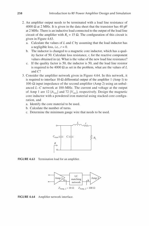
258 Introduction to RF Power Amplifier Design and Simulation
2. An amplifier output needs to be terminated with a load line resistance of 4000 Ω at 2 MHz. It is given in the data sheet that the transistor has 40 pF at 2 MHz. There is an inductive load connected to the output of the load line circuit of the amplifier with RL = 15 Ω. The configuration of this circuit is given in Figure 4.63.
a. Calculate the values of L and C by assuming that the load inductor has a negligible loss, i.e., r = 0.
b. The inductor is changed to a magnetic core inductor, which has a qual-ity factor of 50. Calculate loss resistance, r, for the reactive component values obtained in (a). What is the value of the new load line resistance?
c. If the quality factor is 50, the inductor is 50, and the load line resistor is required to be 4000 Ω as set in the problem, what are the values of L and C?
3. Consider the amplifier network given in Figure 4.64. In this network, it is required to interface 10-Ω differential output of the amplifier 1 (Amp 1) to 100-Ω input impedance of the second amplifier (Amp 2) using an unbal-anced L–C network at 100-MHz. The current and voltage at the output of Amp 1 are 12 [Arms] and 72 [Vrms], respectively. Design the magnetic core inductor with a powdered iron material using stacked core configu-ration, and
a. Identify the core material to be used. b. Calculate the number of turns. c. Determine the minimum gauge wire that needs to be used.
Ctran
R
RL
L
C
r
FIGURE 4.63 Termination load for an amplifier.
Amp 1LC
matchingnetwork
Amp 2
ZAmp_1 = 10 Ω ZAmp_2 = 100 Ω
FIGURE 4.64 Amplifier network interface.
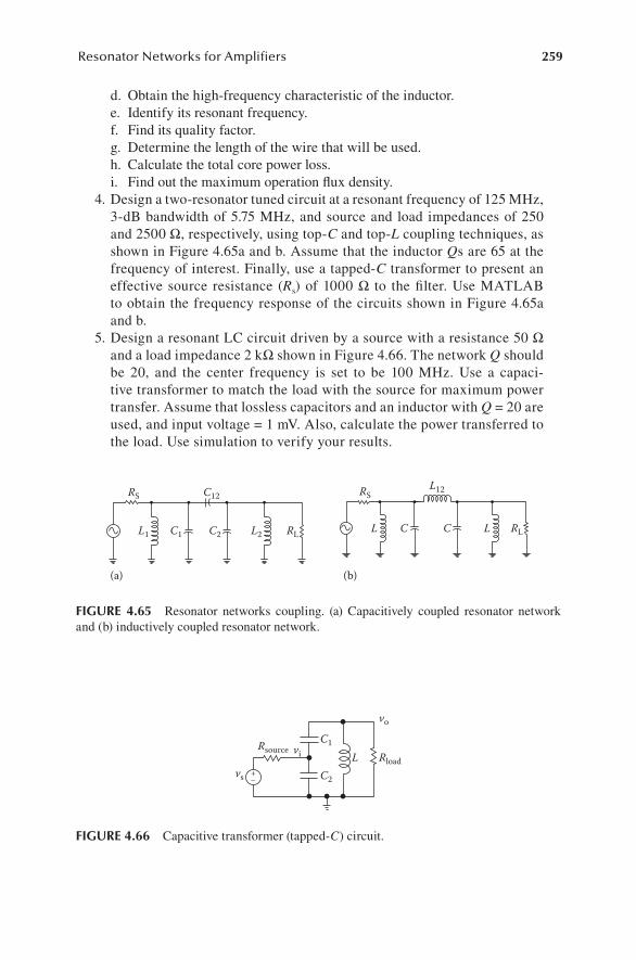
259Resonator Networks for Amplifiers
d. Obtain the high-frequency characteristic of the inductor. e. Identify its resonant frequency. f. Find its quality factor. g. Determine the length of the wire that will be used. h. Calculate the total core power loss. i. Find out the maximum operation flux density.
4. Design a two-resonator tuned circuit at a resonant frequency of 125 MHz, 3-dB bandwidth of 5.75 MHz, and source and load impedances of 250 and 2500 Ω, respectively, using top-C and top-L coupling techniques, as shown in Figure 4.65a and b. Assume that the inductor Qs are 65 at the frequency of interest. Finally, use a tapped-C transformer to present an effective source resistance (Rs) of 1000 Ω to the filter. Use MATLAB to obtain the frequency response of the circuits shown in Figure 4.65a and b.
5. Design a resonant LC circuit driven by a source with a resistance 50 Ω and a load impedance 2 kΩ shown in Figure 4.66. The network Q should be 20, and the center frequency is set to be 100 MHz. Use a capaci-tive transformer to match the load with the source for maximum power transfer. Assume that lossless capacitors and an inductor with Q = 20 are used, and input voltage = 1 mV. Also, calculate the power transferred to the load. Use simulation to verify your results.
+–
C1
C2
L RloadRsource
vo
vi
vs
FIGURE 4.66 Capacitive transformer (tapped-C) circuit.
RS C12
L1 C1 C2 L2 RL
RSL12
L C C L RL
(a) (b)
FIGURE 4.65 Resonator networks coupling. (a) Capacitively coupled resonator network and (b) inductively coupled resonator network.

260 Introduction to RF Power Amplifier Design and Simulation
6. Consider the tuned amplifier circuit given in Figure 4.67. What are the cen-ter frequency, Q, and midband gain of the amplifier if L1 = 5 μH, C1 = 10 pF, Ic = 1 mA, Cπ = 5 pF, RL = 5 kΩ, rπ = 2.5 kΩ, and Cμ = 1 pF?
REFERENCE
1. A. Eroglu. 2013. RF Circuit Design Techniques for MF-UHF Applications. CRC Press, Boca Raton, FL.
C1
C2+ 4
1– +
–
viRLvo
L1
FIGURE 4.67 Tapped-L circuit.
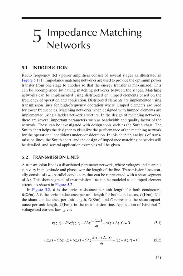
261
5 Impedance Matching Networks
5.1 INTRODUCTION
Radio frequency (RF) power amplifiers consist of several stages as illustrated in Figure 5.1 [1]. Impedance matching networks are used to provide the optimum power transfer from one stage to another so that the energy transfer is maximized. This can be accomplished by having matching networks between the stages. Matching networks can be implemented using distributed or lumped elements based on the frequency of operation and application. Distributed elements are implemented using transmission lines for high-frequency operation where lumped elements are used for lower frequencies. Matching networks when designed with lumped elements are implemented using a ladder network structure. In the design of matching networks, there are several important parameters such as bandwidth and quality factor of the network. These can be investigated with design tools such as the Smith chart. The Smith chart helps the designer to visualize the performance of the matching network for the operational conditions under consideration. In this chapter, analysis of trans-mission lines, the Smith chart, and the design of impedance matching networks will be detailed, and several application examples will be given.
5.2 TRANSMISSION LINES
A transmission line is a distributed-parameter network, where voltages and currents can vary in magnitude and phase over the length of the line. Transmission lines usu-ally consist of two parallel conductors that can be represented with a short segment of Δz. This short segment of transmission line can be modeled as a lumped-element circuit, as shown in Figure 5.2.
In Figure 5.2, R is the series resistance per unit length for both conductors, R(Ω/m), L is the series inductance per unit length for both conductors, L(H/m), G is the shunt conductance per unit length, G(S/m), and C represents the shunt capaci-tance per unit length, C(F/m), in the transmission line. Application of Kirchhoff’s voltage and current laws gives
v z t R zi z t L zi z tt
v z z t( , ) ( , )( , )
( , )− −∂∂
− + =∆ ∆ ∆ 0 (5.1)
i z t G zv z z t C zv z z t
ti z z t( , ) ( , )
( , )( , )− + −
∂ +∂
− + =∆ ∆ ∆∆
∆ 0 (5.2)
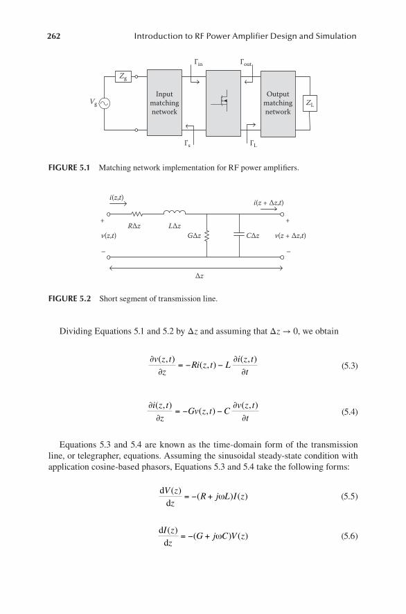
262 Introduction to RF Power Amplifier Design and Simulation
Dividing Equations 5.1 and 5.2 by Δz and assuming that Δz → 0, we obtain
∂∂
= − −∂∂
v z t
zRi z t L
i z t
t
( , )( , )
( , ) (5.3)
∂∂
= − −∂∂
i z t
zGv z t C
v z t
t
( , )( , )
( , ) (5.4)
Equations 5.3 and 5.4 are known as the time-domain form of the transmission line, or telegrapher, equations. Assuming the sinusoidal steady-state condition with application cosine-based phasors, Equations 5.3 and 5.4 take the following forms:
ddV zz
R j L I z( )
( ) ( )= − + ω (5.5)
ddI zz
G j C V z( )
( ) ( )= − + ω (5.6)
Inputmatchingnetwork
Zg
Гs ГL
ГoutГin
ZLVgOutput
matchingnetwork
FIGURE 5.1 Matching network implementation for RF power amplifiers.
+
–
+
–
v(z,t)
i(z,t)
v(z + ∆z,t)
i(z + ∆z,t)
G∆zR∆z L∆z
C∆z
∆z
FIGURE 5.2 Short segment of transmission line.
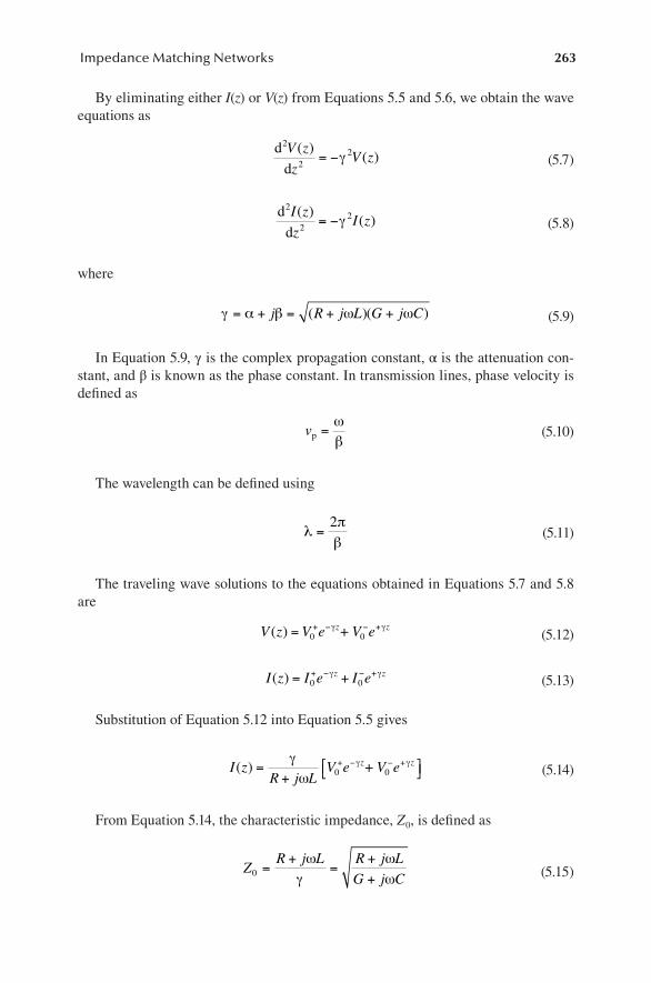
263Impedance Matching Networks
By eliminating either I(z) or V(z) from Equations 5.5 and 5.6, we obtain the wave equations as
d
d
2
22V z
zV z
( )( )= −γ (5.7)
d
d
2
22I z
zI z
( )( )= −γ (5.8)
where
γ α β ω ω= + = + +j R j L G j C( )( ) (5.9)
In Equation 5.9, γ is the complex propagation constant, α is the attenuation con-stant, and β is known as the phase constant. In transmission lines, phase velocity is defined as
vp =ωβ
(5.10)
The wavelength can be defined using
λπβ
=2
(5.11)
The traveling wave solutions to the equations obtained in Equations 5.7 and 5.8 are
V z V e V ez z( ) = + − − +0 0
γ γ+ (5.12)
I z I e I ez z( ) = ++ − − +0 0
γ γ (5.13)
Substitution of Equation 5.12 into Equation 5.5 gives
I zR j L
V e V ez z( ) =+
+ − − +γ
ωγ γ
0 0+ (5.14)
From Equation 5.14, the characteristic impedance, Z0, is defined as
ZR j L R j L
G j C0 =+
=++
ωγ
ωω (5.15)
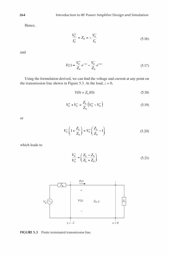
264 Introduction to RF Power Amplifier Design and Simulation
Hence,
V
IZ
V
I0
00
0
0
+
+
−
−= = − (5.16)
and
I zVZ
eVZ
ez z( ) = −+
−−
+0
0
0
0
γ γ (5.17)
Using the formulation derived, we can find the voltage and current at any point on the transmission line shown in Figure 5.3. At the load, z = 0,
V(0) = ZLI(0) (5.18)
V VZZ
V V0 0 0 0+ − + −+ = −( )L
0
(5.19)
or
VZZ
VZZ0 0
− ++
= −
1 1
0 0
L L (5.20)
which leads to
V
V
Z ZZ Z
0
0
−
+=
−+
L
L
0
0 (5.21)
Z0, γVg
Zg
ZL
z = 0z = –l
+
–
V(z)
I(z)
FIGURE 5.3 Finite terminated transmission line.
265Impedance Matching Networks
Equation 5.21 is then defined as the reflection coefficient at the load, and it is expressed as
ΓL =−+
Z ZZ ZL
L
0
0 (5.22)
Voltage and current can be expressed in terms of reflection coefficient as
V( )z V e eyz yz= +( )+ − +0 ΓL (5.23)
I( )zZV e ez z= −( )+ − +1
00
γ γΓL (5.24)
The input impedance can be found at any point on the transmission line shown in Figure 5.4 from
Z zzzin( )( )
( ) =VI
(5.25)
We then have
Z z Ze e
e e
z z
z zin ( ) =+( )−( )
− +
− +0
γ γ
γ γ
Γ
ΓL
L
(5.26)
Zg
+
–
I(z)
Z0, γ
Zin
Vg ZL
z = –l z = 0
V(z)
FIGURE 5.4 Input impedance calculation on the transmission line.
266 Introduction to RF Power Amplifier Design and Simulation
which can be expressed as
Z z Z
Z ZZ Z
e
Z ZZ Z
z
in
L
L
L
L
( ) =
+−+
−−+
+
0
0
0
2
0
0
1
1
γ
=+ + −
+
+
e
ZZ Z Z Z e
Zz
z
20
0 02
γ
γ( ) ( )
(L L
L ++ − −
=+ + −
+
−
Z Z Z e
ZZ Z e Z Z e
z
z
0 02
00 0
) ( )
( ) ( )
L
L L
γ
γ ++
− ++ − −
γ
γ γ
z
z zZ Z e Z Z e( ) ( )L L0 0
(5.27)
Equation 5.27 can be rewritten as
Z z ZZ Z e Z Z e
Z Z e Z
z z
zinL L
L L
( )( ) ( )
( ) (=
+ + −
+ −
− +
−00 0
0
γ γ
γ −−
=+ − −
−
+
+ − + −
Z e
ZZ e e Z e e
Z
z
z z z z
0
00
)
( ) ( )
γ
γ γ γ γL
LL( ) ( )e e Z e ez z z z+ − + −− + +
γ γ γ γ0
(5.28)
which can also be expressed as
Z z ZZ Z zZ Z zinL
L
( )tanh( )tanh( )
=−−
0
0
0
γγ
(5.29)
At the input when z = −l, the impedance can be found from Equation 5.29 as
Z z ZZ Z lZ Z linL
L
( )tanh( )tanh( )
=++
0
0
0
γγ
(5.30)
5.2.1 Limiting Cases for transmission Lines
There are three cases that can be considered as the limiting case for transmission lines. These are lossless lines, low-loss lines, and distortionless lines.
a. Lossless line (R = G = 0) Transmission lines can be considered as lossless when R = G = 0. When
R = G = 0, the defining equations for the transmission lines can be simpli-fied as
γ α β= + = ⇒ =j j LCω α 0 (5.31)
β = ω LC (5.32)
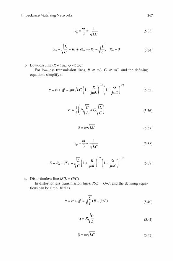
267Impedance Matching Networks
vLC
p = =ωβ
1 (5.33)
ZLC
R jX RLC
X0 0 0 0 0 0= = + ⇒ = =, (5.34)
b. Low-loss line (R ≪ ωL, G ≪ ωC) For low-loss transmission lines, R ≪ ωL, G ≪ ωC, and the defining
equations simplify to
γ α β ωω
= + = +
+
j j LC
R
j L
G
j C1 1
1 2 1 2/ /
ω (5.35)
α ≅ +
12
RC
LG
L
C (5.36)
β ω≅ LC (5.37)
vLC
p = ≅ωβ
1 (5.38)
Z R jXL
C
R
j L
G
j C= + = +
+
−
0 0
1 2 1 2
1 1ω ω
/ /
(5.39)
c. Distortionless line (R/L = G/C) In distortionless transmission lines, R/L = G/C, and the defining equa-
tions can be simplified as
γ α β ω= + = +jC
LR j L( ) (5.40)
α = RC
L (5.41)
β ω= LC (5.42)
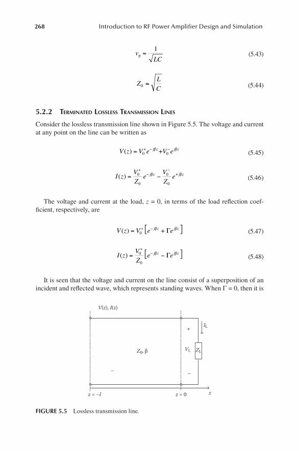
268 Introduction to RF Power Amplifier Design and Simulation
vLC
p =1
(5.43)
ZL
C0 = (5.44)
5.2.2 terminated LossLess transmission Lines
Consider the lossless transmission line shown in Figure 5.5. The voltage and current at any point on the line can be written as
V z V e V ej z j z( ) = + − −0 0
β β+ (5.45)
I zV
Ze
V
Zej z j z( ) = −
+−
−+0
0
0
0
β β (5.46)
The voltage and current at the load, z = 0, in terms of the load reflection coef-ficient, respectively, are
V z V e ej z j z( ) = +[ ]+ −0
β βΓ (5.47)
I zV
Ze ej z j z( ) = −[ ]
+−0
0
β βΓ (5.48)
It is seen that the voltage and current on the line consist of a superposition of an incident and reflected wave, which represents standing waves. When Γ = 0, then it is
+
– –
z
Z0, β
z = –l z = 0
ZL
IL
VL
V(z), I(z)
FIGURE 5.5 Lossless transmission line.
269Impedance Matching Networks
a matched condition. The time–average power flow along the line at the point z can be written as
P V z I zV
Ze ej z j
avg = ∗ = − ∗ ++
−12
12
10
2
0
2 2Re ( ) ( ) Re Γ Γβ βzz − Γ2
(5.49)
or
PV
Zavg = −( )+1
210
2
0
2Γ (5.50)
When the load is mismatched, not all of the available power from the generator is delivered to the load. The power that is lost is known as return loss, RL, and this can be found from
RL dB= −20 log Γ (5.51)
Under a mismatched condition, the voltage on the line can be written as
V z V e V e V ej z j l j l( ) ( )= + = + = ++ + − + −0
20
20
21 1 1Γ Γ Γβ β θ β (5.52)
The minimum and maximum values of the voltage from Equation 5.42 are found as
V V V Vmax min= +( ) = −( )+ +0 01 1Γ Γand (5.53)
A measure of the mismatch of a line called the voltage standing wave ratio (VSWR) can be expressed as the ratio of the maximum voltage to the minimum voltage as
VSWR = =+
−
VVmax
min
1
1
Γ
Γ (5.54)
From Equation 5.52, the distance between two successive voltage maxima (or minima) is l = 2π/2β = λ/2 (2βl = 2π), whereas the distance between a maximum and a minimum is l = π/2β = λ/4. From Equation 5.48, with z = −l,
Γ Γ( ) ( )lV e
V ee
j l
j lj l= =
− −
+−0
0
20β
ββ
(5.55)

270 Introduction to RF Power Amplifier Design and Simulation
For the current,
I( ) ( )z V eZ
ej z j l=
−( )+ − + −
0β φ β1
10
2Γ (5.56)
or
I( ) ( )z VZ
e j l=
−+ + −
01
10
2Γ φ β (5.57)
Hence, the maximum and minimum values of the current on the line can be writ-ten as
I I z VZmax max
( )= =
+( )+
01
10
Γ (5.58)
I I z VZmin min
( )= =
−( )+
01
10
Γ (5.59)
The current standing wave ratio, ISWR, is
ISWR = =+
−
IImax
min
1
1
Γ
Γ (5.60)
Hence, VSWR = ISWR from Equations 5.54 and 5.60. VSWR will be used throughout the book for analysis. The voltage waveform vs. the length of the trans-mission line along the axis is plotted in Figure 5.6.
z = 0z∆z = λ/2
1 + |ΓL|
1 – |ΓL|
1
FIGURE 5.6 Voltage vs. transmission line length.
271Impedance Matching Networks
At a distance l = −z, the input impedance is then equal to
ZV lI l
ZZ jZ lZ jZ linL
L
=−−
=++
( )( )
tantan0
0
0
ββ
(5.61)
Example
A 2-m lossless, air-spaced transmission line having a characteristic impedance 50 Ω is terminated with an impedance 40 + j30 (Ω) at an operating frequency of 200 MHz. Find the input impedance.
Solution
The phase constant is found from
βω
π= =vp
43
Since it is given that R0 = 50 Ω, ZL = 40 + j30, and ℓ = 2 m, the input impedance is obtained from Equation 5.61 as
Z
j j
j ji =
+ + ⋅ ⋅
+ + ⋅
5040 30 50
43
2
50 40 30
( ) tan
( ) ta
π
nn. .
43
226 3 9 87
π⋅
= − j
Example
For a transmission, it is given that ZL = 17.4 − j30 [Ω] and Z0 = 50 [Ω]. Calculate ΓL, SWR, zmin, Vmax, and Vmin on the transmission line.
Solution
From the given information, we find the load reflection coefficient as
ΓLL
L
ZZ
=−+
= − − = −ZZ
j e j0
0
1 990 24 0 55 0 6. . . ( . )
The VSWR is found from
SWR L
L
= =+
−=
+−
=VVmax
min
.
..
1
11 0 61 0 6
4 0Γ
Γ
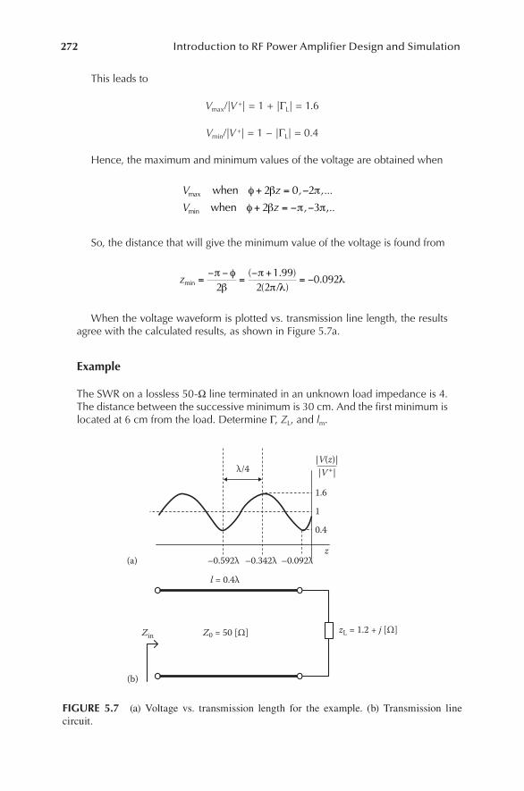
272 Introduction to RF Power Amplifier Design and Simulation
This leads to
Vmax/|V +| = 1 + |ΓL| = 1.6
Vmin/|V +| = 1 − |ΓL| = 0.4
Hence, the maximum and minimum values of the voltage are obtained when
V z , ,...
V z , ..max
min ,
when
when
φ β π
φ β π π
+ = −
+ = − −
2 0 2
2 3
So, the distance that will give the minimum value of the voltage is found from
zmin( . )
( ).=
− −=
− += −
π φβ
ππ λ
λ2
1 992 2
0 092/
When the voltage waveform is plotted vs. transmission line length, the results agree with the calculated results, as shown in Figure 5.7a.
Example
The SWR on a lossless 50-Ω line terminated in an unknown load impedance is 4. The distance between the successive minimum is 30 cm. And the first minimum is located at 6 cm from the load. Determine Γ, ZL, and lm.
Zin Z0 = 50 [Ω]
l = 0.4λ
(a)
(b)
zL = 1.2 + j [Ω]
–0.592λ –0.342λ –0.092λ
λ/4|V(z)||V +|
1.6
1
0.4
z
FIGURE 5.7 (a) Voltage vs. transmission length for the example. (b) Transmission line circuit.
273Impedance Matching Networks
Solution
From the given information, the wavelength can be found as
λλ β
πλ
π2
0 3 0 62
3 33= ⇒ = = =. . , .m
The reflection coefficient is equal to
Γ =−+
= ′ = ⇒ = − ′ =4 14 1
0 6 0 062
0 24. , . .z zm m mm mλ
θ β π π θ πΓ Γ Γ Γ= ′ − = − = = = − −−2 0 6 0 6 0 185 0 90 6z e e jm
j j. , . . .. 55
The load impedance is then equal to
Z ZjjL
L
L
=+−
= ⋅+ − −− − −0
11
501 0 185 0 951 0 185 0 9
ΓΓ
( . . )( . . 55
1 43 41 17)
. .= − j
Example
Calculate the parameters given below for the transmission line shown in Figure 5.7b when a normalized load of 1.2 + j [Ω] is connected.
a. The VSWR on the line b. Load reflection coefficient c. Admittance of the load d. Impedance at the input of the line e. The distance from the load to the first voltage minimum f. The distance from the load to the first voltage maximum
Solution
Since the load impedance is already normalized, we can skip the normalization process and start calculations as
a. SWR = 2.5 b. ΓL = 0.42 ∠ 54.5°
c. YyZ
jjL
L mS= =−
= −0
0 5 0 4250
10 8 4. .
( . )Ω
d. Zin = zin · Z0 = (0.5 + j0.4) · Z0 = (25 + j20) Ω e. ℓmin = 0.5λ − 0.174λ = 0.326λ f . ℓmax = 0.25λ − 0.174λ = 0.076λ
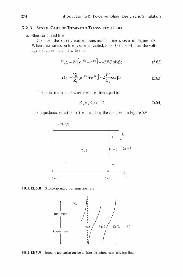
274 Introduction to RF Power Amplifier Design and Simulation
5.2.3 speCiaL Cases of terminated transmission Lines
a. Short-circuited line Consider the short-circuited transmission line shown in Figure 5.8.
When a transmission line is short circuited, ZL = 0 → Γ = −1, then the volt-age and current can be written as
V z V e e jV zj z j z( ) sin= −[ ] = −+ − +0 02β β β (5.62)
I zVZ
e eVZ
zj z j z( ) cos= +[ ] =+
−+
0
0
0
0
2β β β (5.63)
The input impedance when z = −l is then equal to
Zin = jZ0 tan βl (5.64)
The impedance variation of the line along the z is given in Figure 5.9.
+
Z0, β
z = –l z = 0
–
V(z), I(z)
–
IL
z
ZL = 0VL = 0
FIGURE 5.8 Short-circuited transmission line.
Inductive
Xin
βl5π/23π/2π/2Capacitive
FIGURE 5.9 Impedance variation for a short-circuited transmission line.
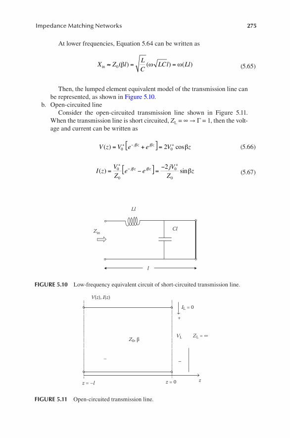
275Impedance Matching Networks
At lower frequencies, Equation 5.64 can be written as
X Z lLC
LCl Llin ≈ = =0( ) ( ) ( )β ω ω (5.65)
Then, the lumped element equivalent model of the transmission line can be represented, as shown in Figure 5.10.
b. Open-circuited line Consider the open-circuited transmission line shown in Figure 5.11.
When the transmission line is short circuited, ZL = ∞ → Γ = 1, then the volt-age and current can be written as
V z V e e V zj z j z( ) cos= +[ ] =+ − +0 02β β β (5.66)
I zVZ
e ejVZ
zj z j z( ) sin= −[ ] = −+−
+0
0
0
0
2β β β (5.67)
Zin
Ll
Cl
l
FIGURE 5.10 Low-frequency equivalent circuit of short-circuited transmission line.
+
ZL = ∞Z0, β
z = 0z = –l
–
V(z), I(z)
VL
–
IL = 0
z
FIGURE 5.11 Open-circuited transmission line.
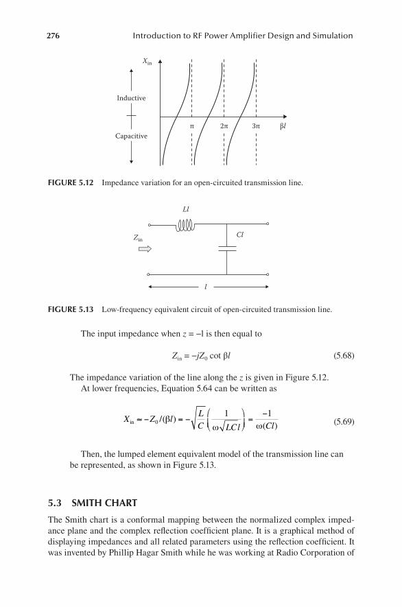
276 Introduction to RF Power Amplifier Design and Simulation
The input impedance when z = −l is then equal to
Zin = −jZ0 cot βl (5.68)
The impedance variation of the line along the z is given in Figure 5.12. At lower frequencies, Equation 5.64 can be written as
X Z lLC LCl Clin /≈ − = −
=
−0
1 1( )
( )β
ω ω (5.69)
Then, the lumped element equivalent model of the transmission line can be represented, as shown in Figure 5.13.
5.3 SMITH CHART
The Smith chart is a conformal mapping between the normalized complex imped-ance plane and the complex reflection coefficient plane. It is a graphical method of displaying impedances and all related parameters using the reflection coefficient. It was invented by Phillip Hagar Smith while he was working at Radio Corporation of
Inductive
Xin
βl3π2ππCapacitive
FIGURE 5.12 Impedance variation for an open-circuited transmission line.
Zin
Ll
Cl
l
FIGURE 5.13 Low-frequency equivalent circuit of open-circuited transmission line.

277Impedance Matching Networks
America (RCA). The process of establishing the Smith chart begins with normal-izing the impedance, as shown by
zZZ
R jXZL
L L L= =+
0 0
(5.70)
Now, consider the right-hand portion of the normalized complex impedance plane, as illustrated in Figure 5.14. All values of impedance such that R ≥ 0 are represented by points in the plane. The impedance of all passive devices will be represented by points in the right-half plane.
The complex reflection coefficient may be written as a magnitude and a phase or as real and imaginary parts.
Γ Γ Γ ΓΓL L Lr Li
L= = +∠e j (5.71)
The reflection coefficient in terms of the load ZL terminating line Z0 is defined as
ΓLL
L
=−+
Z ZZ Z
0
0
(5.72)
The above equation can be rearranged to get
Z ZLL
L
=+−0
11
ΓΓ
(5.73)
In terms of normalized quantities, Equation 5.73 can be written as
z r jxZZL L LL L
L
= + = =+−0
11
ΓΓ
(5.74)
xL
rLA
B
C1
1
FIGURE 5.14 Right-hand portion of the normalized complex impedance plane.

278 Introduction to RF Power Amplifier Design and Simulation
Substituting in the complex expression for ΓL and equating real and imaginary parts, we find the two equations that represent circles in the complex reflection coef-ficient plane as
Γ ΓLrL
LLi
L
−+
+ − =
+
rr r1
01
1
2
2
2
( ) (5.75)
( )Γ ΓLr LiL L
− + −
=
1
1 12
2 2
x x (5.76)
The first circle is centered at
rr
L
L10
+, (5.77)
and the second circle is centered at
11
,xL
(5.78)
The location of the first circle that is always inside the unit circle in the complex reflection coefficient plane with the corresponding radius is
1
1+ rL (5.79)
Hence, this circle will always be fully contained within the unit circle because the radius can never be greater than unity. This conformal mapping represents the mapping of the real resistance circle and is shown in Figure 5.15 using the mapping equation:
Γ Γr L−+
+ =
+
rr r1
11
2
2
2
( ) (5.80)
The location of the second circle that is always outside the unit circle in the com-plex reflection coefficient plane with the corresponding radius is
1xL
(5.81)
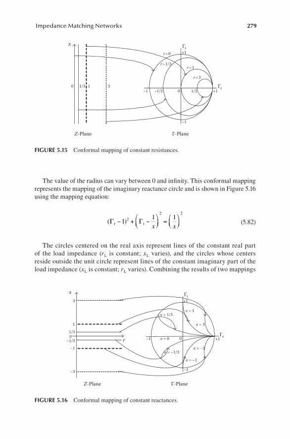
279Impedance Matching Networks
The value of the radius can vary between 0 and infinity. This conformal mapping represents the mapping of the imaginary reactance circle and is shown in Figure 5.16 using the mapping equation:
( )Γ Γr i− + −
=
11 12
2 2
x x (5.82)
The circles centered on the real axis represent lines of the constant real part of the load impedance (rL is constant; xL varies), and the circles whose centers reside outside the unit circle represent lines of the constant imaginary part of the load impedance (xL is constant; rL varies). Combining the results of two mappings
1/2 +10–1/2–1
+1
r = 1
r = 3
r = 1/3
r = 0
–1
x
0 1/3 1 3
Z-Plane Г-Plane
Гi
Гr
FIGURE 5.15 Conformal mapping of constant resistances.
Гi
Гrr 0
+1
x
01/3
1
3
Z-Plane Г-Plane
x = 0
x = 1/3
x = –1/3
x = –1
x = –3
x = 1
x = 3
–1/3–1
–3
+1
–1
–1
FIGURE 5.16 Conformal mapping of constant reactances.

280 Introduction to RF Power Amplifier Design and Simulation
into a single mapping gives the display of the complete Smith chart, as shown in Figure 5.17.
In summary, the properties of the r-circles are as follows:
• The centers of all r-circles lie on the Γr-axis.• The r = 0 circle, having a unity radius and centered at the origin, is the
largest.• The r-circles become progressively smaller as r increases from 0 to ∞, end-
ing at the (Γr = 1, Γi = 0) point for an open circuit.• All r circles pass through the (Γr = 1, Γi = 0) point.
Similarly, the properties of the x-circles are as follows:
• The centers of all x-circles lie on the Γr = 1 line, those for x > 0 (inductive reactance) lie above the Γr-axis, and those for x < 0 (capacitive reactance) lie below the Γr-axis.
• The x = 0 circle becomes the Γr-axis.• The x-circle becomes progressively smaller as |x| increases from 0 to ∞,
ending at the (Γr = 1, Γi = 0) point for an open circuit.• All x circles pass through the (Γr = 1, Γi = 0) point.
Hence, in the combined display of the Smith chart,
• All ǀΓǀ circles are centered at the origin, and their radii vary uniformly from 0 to 1.
• The angle, measured from the positive real axis, of the line drawn from the origin through the point representing zL equals θΓ.
• The value of the r circle passing through the intersection of the ǀΓǀ-circle and the positive-real axis equals the standing-wave ratio SWR.
x = 3
x = –3x = –1/3
r = 1/3x = 1/3
x = 0
x = –1
r = 3
x = 1
r 0–1 +1
+1
–1
01/3
1
3
–1/3–1
–3
r = 1
r = 0
1/3 1 3
x
Z-Plane Г-Plane
Гr
Гi
FIGURE 5.17 Combined conformal mapping leading to the display of the Smith chart.

281Impedance Matching Networks
Example
Locate the following normalized impedances on the Smith chart, and calculate the standing wave ratios and reflection coefficients: (a) z = 0.2 + j0.5; (b) z = 0.4 + j0.7; (c) z = 0.6 + j0.1.
Solution
The generic MATLAB® code given below is developed to calculate mark imped-ance points, draw VSWR circles, and calculate reflection coefficients on the Smith chart at single frequency.
%This program marks impedance points, draws VSWR circle, calculates%reflection coefficients, and marks them on the Smith Chart at single%frequency
clear all;close all;global Z0;Set_Z0(1); %Set Z0 to 1 %Gui Prompt prompt = 'ZL1', 'ZL2: ','ZL3';dlg_title = 'Enter Impedance ';num_lines = 1;def = '0.2+j*0.5','0.4+j*0.7','0.6+j*0.1';answer = inputdlg(prompt,dlg_title,num_lines,def, 'on'); %convert the strings received from the GUI to numbersvaluearray=str2double(answer); %Give variable names to the received numbersZL1=valuearray(1);ZL2=valuearray(2);ZL3=valuearray(3); %part agamma1=(ZL1-Z0)/(ZL1+Z0);VSWR1=(1+abs(gamma1))/(1-abs(gamma1));[th1,rl1]=cart2pol(real(gamma1),imag(gamma1));smith; %Call Smith Chart Programs_point(ZL1);const_SWR_circle(ZL1,'r--');hold on;text(real(gamma1)+0.04,imag(gamma1)-0.03,'\bf\Gamma_1');%part bgamma2=(ZL2-Z0)/(ZL2+Z0);VSWR2=(1+abs(gamma2))/(1-abs(gamma2));[th2,rl2]=cart2pol(real(gamma2),imag(gamma2));s_point(ZL2);
%part cgamma3=(ZL3-Z0)/(ZL3+Z0);VSWR3=(1+abs(gamma3))/(1-abs(gamma3));[th3,rl3]=cart2pol(real(gamma3),imag(gamma3));s_point(ZL3);

282 Introduction to RF Power Amplifier Design and Simulation
const_SWR_circle(ZL3,'r--');hold on;text(real(gamma3)+0.04,imag(gamma3)-0.03,'\bf\Gamma_3'); msgbox( sprintf([... 'Calculated Parameters for Z1 \n'... ' Reflection coefficient for Z1: gamma1 =%f +j(%f)\n'... ' Reflection Coefficent for Z1 In Polar form
:|gamma1|=%f,angle1=%f\n'... ' Standing Wave Ratio for Z1 : VSWR1=%f \n'... '\n'... 'Calculated Parameters for Z2 \n'... ' Reflection coefficient for Z2: gamma2 =%f +j(%f)\n'... ' Reflection Coefficent for Z2 In Polar form
:|gamma2|=%f,angle1=%f\n'... ' Standing Wave Ratio for Z2 : VSWR2=%f \n'... '\n'... 'Calculated Parameters for Z3 \n'... ' Reflection coefficient for Z3: gamma3 =%f +j(%f)\n'... ' Reflection Coefficient for Z3 In Polar form
:|gamma3|=%f,angle3=%f\n'... ' Standing Wave Ratio for Z3: VSWR3=%f \n'... '\n']... ,real(gamma1),imag(gamma1),rl1,th1*180/pi,VSWR1,real(gamma2),imag(gamma2), rl2,th2*180/pi,VSWR2,real(gamma3),imag(gamma3),rl3,th3*180/pi,VSWR3));
When the program is executed, a GUI is displayed, as shown in Figure 5.18a, for entering impedances and the result. The results are displayed on the Smith chart in Figure 5.18b.
5.3.1 input impedanCe determination with smith Chart
It was shown before that the voltage and current at any point on the transmission line can be expressed as
V zI
Z Z e ez z( ) ( ) [ ]′ = + +′ − ′LL2
102γ γΓ (5.83)
I zIZ
Z Z e ez z( ) ( ) [ ]′ = + −′ − ′LL2
10
02γ γΓ (5.84)
where z′ = l − z. Then, the input impedance at a distance d away from the load on the line in terms of reflection coefficient can be obtained as
Z dV dI d
Zdd
( )( )( )
( )( )
= =+−0
11
ΓΓ
(5.85)
where Γ(d) = ΓLe−j2βd (5.86)
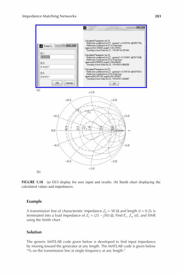
283Impedance Matching Networks
Example
A transmission line of characteristic impedance Z0 = 50 Ω and length d = 0.2λ is terminated into a load impedance of ZL = (25 − j50) Ω. Find ΓL, Zin (d), and SWR using the Smith chart.
Solution
The generic MATLAB code given below is developed to find input impedance by moving toward the generator at any length. The MATLAB code is given below “% on the transmission line at single frequency at any length.”
+1.0
Г1 Г2
Г3
+2.0+0.5
–2.0–0.5
–1.0
+5.0
–5.0
+0.2
0.2
0.5
1.0
2.0
5.0
–0.2
0.0 ∞
(a)
(b)
FIGURE 5.18 (a) GUI display for user input and results. (b) Smith chart displaying the calculated values and impedances.

284 Introduction to RF Power Amplifier Design and Simulation
%This program find input impedance by moving towards generator%on the transmission line at single frequency at any length
clear all;close all;global Z0;%Gui Prompt
prompt = 'Enter Load Impedance ZL :', 'Enter the Length (in lambda) d :','Enter Characteristic Impedance Z0:';dlg_title = 'Enter Impedance ';num_lines = 1;def = '25-j*50','.2','50';answer = inputdlg(prompt,dlg_title,num_lines,def, 'on');%convert the strings received from the GUI to numbersvaluearray=str2double(answer); %Give variable names to the received numbersZL=valuearray(1);d=valuearray(2);Z0=valuearray(3);
Set_Z0(Z0);gamma_0=(ZL-Z0)/(ZL+Z0);[th0,mag_gamma_0]=cart2pol(real(gamma_0),imag(gamma_0));if th0<0 th0=th0+2*pi;endth_in=th0-2*2*pi*d;if th_in<0 th_in=th_in+2*pi;end [x_gamma_in,y_gamma_in]=pol2cart(th_in,mag_gamma_0);Zin=Z0*(1+x_gamma_in+j*y_gamma_in)/(1-x_gamma_in-j*y_gamma_in);SWR=(1+abs(gamma_0))/(1-abs(gamma_0));smith_chart(0);hold on;th=th0:(th_in-th0)/29:th_in;gamma=mag_gamma_0*ones(1,30);polar(th,gamma,'k');hold ons_point(Zin);text(x_gamma_in+0.04,y_gamma_in-0.03,'\bfZ_in');s_point(ZL);text(real(gamma_0)+0.04,imag(gamma_0)-0.03,'\bfZ_L'); msgbox( sprintf([... 'Calculated Parameters for Transmission Line \n'... ' Load Reflection coefficient : gamma_0 =%f +j(%f)\n'... ' Magnitude of Load Reflection Coefficient :|gamma_0|=%f,angle=%f\n'... ' Input Impedance Zin : Zin=%f +j(%f)\n'... ' Standing Wave Ratio : SWR=%f \n'... '\n']...,real(gamma_0),imag(gamma_0),mag_gamma_0,th0*180/pi,real(Zin), imag(Zin),SWR));
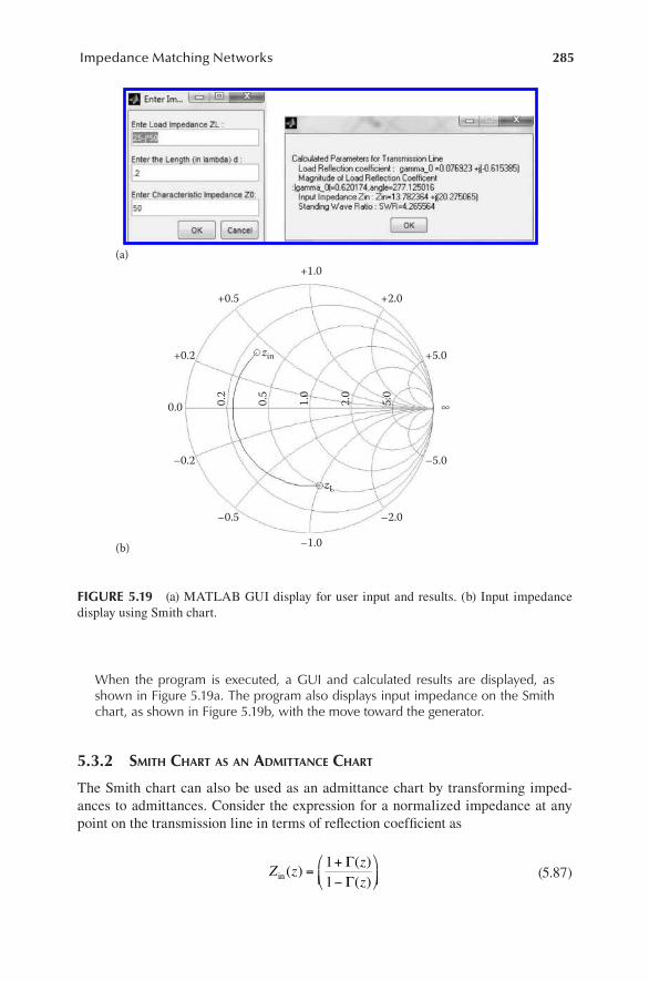
285Impedance Matching Networks
When the program is executed, a GUI and calculated results are displayed, as shown in Figure 5.19a. The program also displays input impedance on the Smith chart, as shown in Figure 5.19b, with the move toward the generator.
5.3.2 smith Chart as an admittanCe Chart
The Smith chart can also be used as an admittance chart by transforming imped-ances to admittances. Consider the expression for a normalized impedance at any point on the transmission line in terms of reflection coefficient as
Z zzzin ( )( )( )
=+−
11
ΓΓ
(5.87)
+1.0
zin
zL
+2.0+0.5
–2.0–0.5
–1.0
+5.0
–5.0
+0.2
0.2
0.5
1.0
2.0
5.0
–0.2
0.0 ∞
(a)
(b)
FIGURE 5.19 (a) MATLAB GUI display for user input and results. (b) Input impedance display using Smith chart.
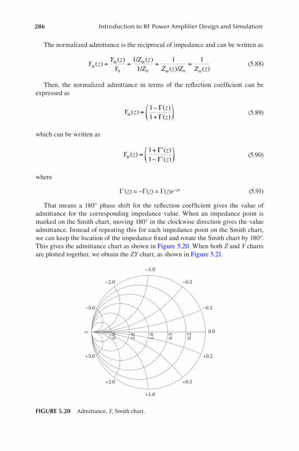
286 Introduction to RF Power Amplifier Design and Simulation
The normalized admittance is the reciprocal of impedance and can be written as
Y zY zY
Z zZ Z z Z Z zin
in in
in in
// /
( )( ) ( )
( ) ( )= = = =
0 0 0
11
1 1 (5.88)
Then, the normalized admittance in terms of the reflection coefficient can be expressed as
Y zzzin ( )( )( )
=−+
11
ΓΓ
(5.89)
which can be written as
Y zzzin ( )( )( )
=+ ′− ′
11
ΓΓ
(5.90)
where
Γ′(z) = −Γ(z) = Γ(z)e−jπ (5.91)
That means a 180° phase shift for the reflection coefficient gives the value of admittance for the corresponding impedance value. When an impedance point is marked on the Smith chart, moving 180° in the clockwise direction gives the value admittance. Instead of repeating this for each impedance point on the Smith chart, we can keep the location of the impedance fixed and rotate the Smith chart by 180°. This gives the admittance chart as shown in Figure 5.20. When both Z and Y charts are plotted together, we obtain the ZY chart, as shown in Figure 5.21.
–1.0
–0.5
–0.2
0.0
0.2
0.5
1.0
2.0
5.0
+0.2
+0.5
–2.0
–5.0
∞
+5.0
+2.0
+1.0
FIGURE 5.20 Admittance, Y, Smith chart.
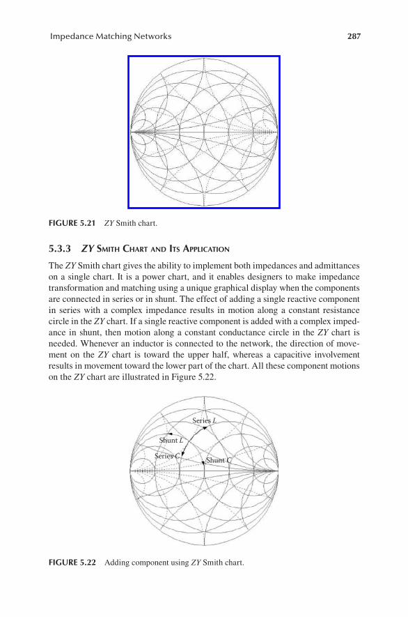
287Impedance Matching Networks
5.3.3 ZY smith Chart and its appLiCation
The ZY Smith chart gives the ability to implement both impedances and admittances on a single chart. It is a power chart, and it enables designers to make impedance transformation and matching using a unique graphical display when the components are connected in series or in shunt. The effect of adding a single reactive component in series with a complex impedance results in motion along a constant resistance circle in the ZY chart. If a single reactive component is added with a complex imped-ance in shunt, then motion along a constant conductance circle in the ZY chart is needed. Whenever an inductor is connected to the network, the direction of move-ment on the ZY chart is toward the upper half, whereas a capacitive involvement results in movement toward the lower part of the chart. All these component motions on the ZY chart are illustrated in Figure 5.22.
FIGURE 5.21 ZY Smith chart.
Series L
Series C
Shunt L
Shunt C
FIGURE 5.22 Adding component using ZY Smith chart.
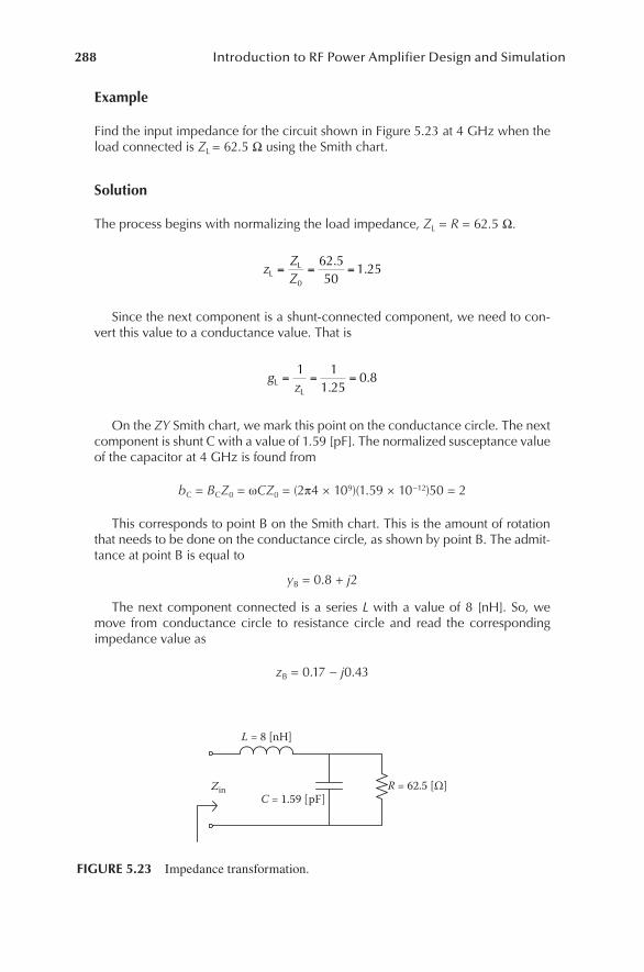
288 Introduction to RF Power Amplifier Design and Simulation
Example
Find the input impedance for the circuit shown in Figure 5.23 at 4 GHz when the load connected is ZL = 62.5 Ω using the Smith chart.
Solution
The process begins with normalizing the load impedance, ZL = R = 62.5 Ω.
zZZLL
0
= = =62 550
1 25.
.
Since the next component is a shunt-connected component, we need to con-vert this value to a conductance value. That is
gzLL
= = =1 1
1 250 8
..
On the ZY Smith chart, we mark this point on the conductance circle. The next component is shunt C with a value of 1.59 [pF]. The normalized susceptance value of the capacitor at 4 GHz is found from
bC = BCZ0 = ωCZ0 = (2π4 × 10⁹)(1.59 × 10⁻¹²)50 = 2
This corresponds to point B on the Smith chart. This is the amount of rotation that needs to be done on the conductance circle, as shown by point B. The admit-tance at point B is equal to
yB = 0.8 + j2
The next component connected is a series L with a value of 8 [nH]. So, we move from conductance circle to resistance circle and read the corresponding impedance value as
zB = 0.17 − j0.43
Zin R = 62.5 [Ω]
L = 8 [nH]
C = 1.59 [ pF ]
FIGURE 5.23 Impedance transformation.
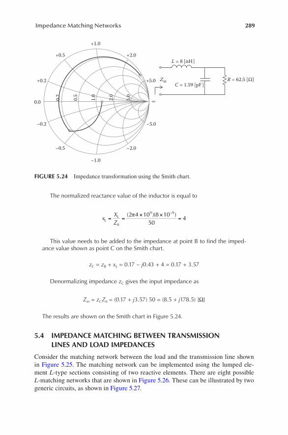
289Impedance Matching Networks
The normalized reactance value of the inductor is equal to
xXZLL= =
× ×=
−
0
9 92 4 10 8 1050
4( )( )π
This value needs to be added to the impedance at point B to find the imped-ance value shown as point C on the Smith chart.
zC = zB + xL = 0.17 − j0.43 + 4 = 0.17 + 3.57
Denormalizing impedance zC gives the input impedance as
Zin = zCZ0 = (0.17 + j3.57) 50 = (8.5 + j178.5) [Ω]
The results are shown on the Smith chart in Figure 5.24.
5.4 IMPEDANCE MATCHING BETWEEN TRANSMISSION LINES AND LOAD IMPEDANCES
Consider the matching network between the load and the transmission line shown in Figure 5.25. The matching network can be implemented using the lumped ele-ment L-type sections consisting of two reactive elements. There are eight possible L-matching networks that are shown in Figure 5.26. These can be illustrated by two generic circuits, as shown in Figure 5.27.
+1.0
+2.0
+5.0 Zin
L = 8 [nH ]
C = 1.59 [pF ]R = 62.5 [Ω]
∞5.0
2.0
1.0
0.5
0.2
–5.0
–2.0
+0.5
+0.2
0.0
–0.2
–0.5
–1.0
FIGURE 5.24 Impedance transformation using the Smith chart.
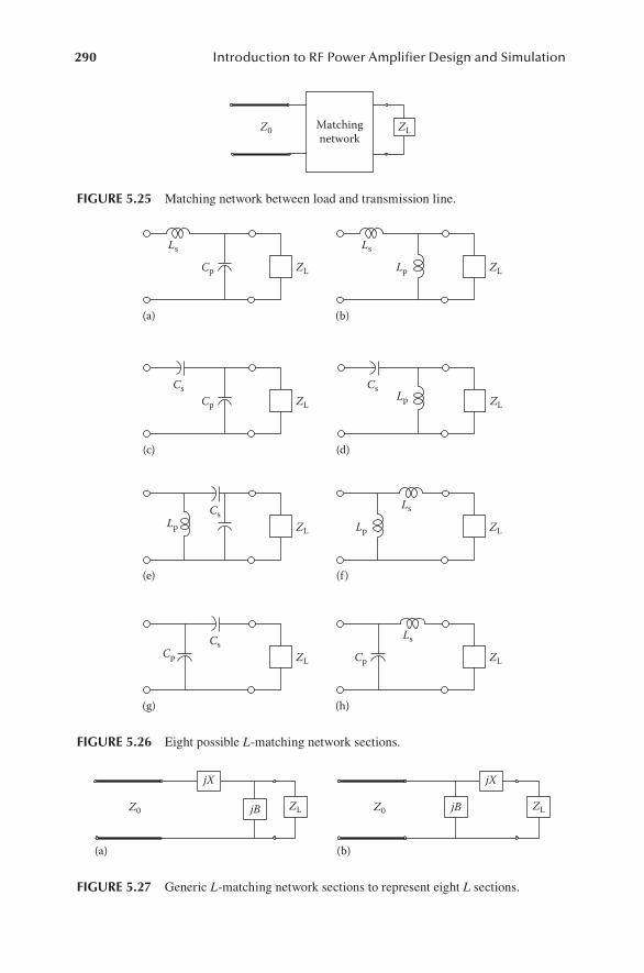
290 Introduction to RF Power Amplifier Design and Simulation
Z0 ZLMatchingnetwork
FIGURE 5.25 Matching network between load and transmission line.
Ls
Cp ZL
(a)
Ls
Lp ZL
(b)
Ls
Lp ZL
(f )
CsCp ZL
(c)
CsLp ZL
(d)
CsLp ZL
(e)
Ls
Cp ZL
(h)
CsCp ZL
(g)
FIGURE 5.26 Eight possible L-matching network sections.
jX
jB
jX
jBZ0 ZL ZLZ0
(a) (b)
FIGURE 5.27 Generic L-matching network sections to represent eight L sections.
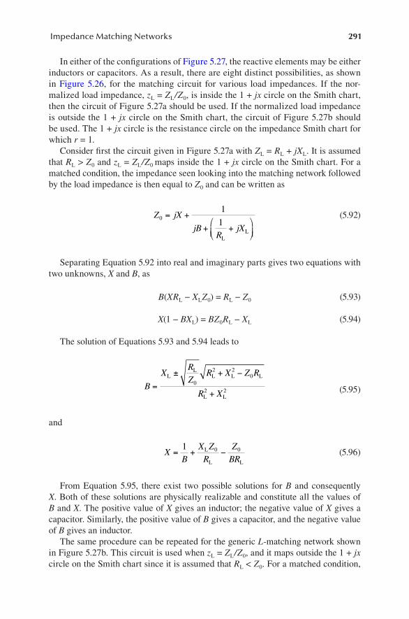
291Impedance Matching Networks
In either of the configurations of Figure 5.27, the reactive elements may be either inductors or capacitors. As a result, there are eight distinct possibilities, as shown in Figure 5.26, for the matching circuit for various load impedances. If the nor-malized load impedance, zL = ZL/Z0, is inside the 1 + jx circle on the Smith chart, then the circuit of Figure 5.27a should be used. If the normalized load impedance is outside the 1 + jx circle on the Smith chart, the circuit of Figure 5.27b should be used. The 1 + jx circle is the resistance circle on the impedance Smith chart for which r = 1.
Consider first the circuit given in Figure 5.27a with ZL = RL + jXL. It is assumed that RL > Z0 and zL = ZL/Z0 maps inside the 1 + jx circle on the Smith chart. For a matched condition, the impedance seen looking into the matching network followed by the load impedance is then equal to Z0 and can be written as
Z jX
jBR
jX0
1
1= +
+ +L
L
(5.92)
Separating Equation 5.92 into real and imaginary parts gives two equations with two unknowns, X and B, as
B(XRL − XLZ0) = RL − Z0 (5.93)
X(1 − BXL) = BZ0RL − XL (5.94)
The solution of Equations 5.93 and 5.94 leads to
B
XRZ
R X Z R
R X=
± + −
+
LL
L L L
L L
0
2 20
2 2 (5.95)
and
XB
X ZR
ZBR
= + −1 0 0L
L L
(5.96)
From Equation 5.95, there exist two possible solutions for B and consequently X. Both of these solutions are physically realizable and constitute all the values of B and X. The positive value of X gives an inductor; the negative value of X gives a capacitor. Similarly, the positive value of B gives a capacitor, and the negative value of B gives an inductor.
The same procedure can be repeated for the generic L-matching network shown in Figure 5.27b. This circuit is used when zL = ZL/Z0, and it maps outside the 1 + jx circle on the Smith chart since it is assumed that RL < Z0. For a matched condition,
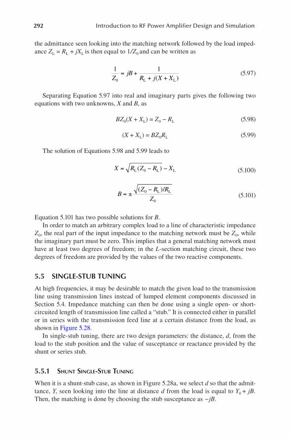
292 Introduction to RF Power Amplifier Design and Simulation
the admittance seen looking into the matching network followed by the load imped-ance ZL = RL + jXL is then equal to 1/Z0 and can be written as
1 1
0ZjB
R j X X= +
+ +L L( ) (5.97)
Separating Equation 5.97 into real and imaginary parts gives the following two equations with two unknowns, X and B, as
BZ0(X + XL) = Z0 − RL (5.98)
(X + XL) = BZ0RL (5.99)
The solution of Equations 5.98 and 5.99 leads to
X R Z R X= − −L L L( )0 (5.100)
BZ R R
Z= ±
−( )0
0
L L/ (5.101)
Equation 5.101 has two possible solutions for B.In order to match an arbitrary complex load to a line of characteristic impedance
Z0, the real part of the input impedance to the matching network must be Z0, while the imaginary part must be zero. This implies that a general matching network must have at least two degrees of freedom; in the L-section matching circuit, these two degrees of freedom are provided by the values of the two reactive components.
5.5 SINGLE-STUB TUNING
At high frequencies, it may be desirable to match the given load to the transmission line using transmission lines instead of lumped element components discussed in Section 5.4. Impedance matching can then be done using a single open- or short-circuited length of transmission line called a “stub.” It is connected either in parallel or in series with the transmission feed line at a certain distance from the load, as shown in Figure 5.28.
In single-stub tuning, there are two design parameters: the distance, d, from the load to the stub position and the value of susceptance or reactance provided by the shunt or series stub.
5.5.1 shunt singLe-stub tuning
When it is a shunt-stub case, as shown in Figure 5.28a, we select d so that the admit-tance, Y, seen looking into the line at distance d from the load is equal to Y0 + jB. Then, the matching is done by choosing the stub susceptance as −jB.
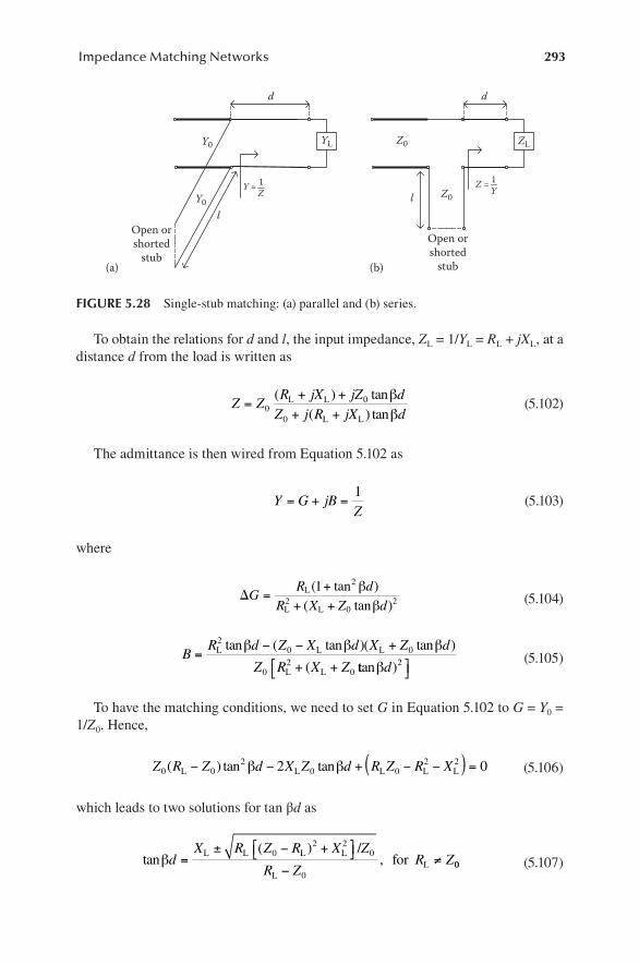
293Impedance Matching Networks
To obtain the relations for d and l, the input impedance, ZL = 1/YL = RL + jXL, at a distance d from the load is written as
Z ZR jX jZ dZ j R jX d
=+ ++ +0
0
0
( ) tan( ) tan
L L
L L
ββ
(5.102)
The admittance is then wired from Equation 5.102 as
Y G jBZ
= + =1
(5.103)
where
=+ β
+ + βG R d
R X Z d(1 tan )( tan )L
2
L2
L 02 (5.104)
BR d Z X d X Z d
Z R X Z=
− − +
+ +L L L
L L
20 0
02
0
tan ( tan )( tan )
(
β β β
ttan )βd 2 (5.105)
To have the matching conditions, we need to set G in Equation 5.102 to G = Y0 = 1/Z0. Hence,
Z R Z d X Z d R Z R X0 02
0 02 22 0( ) tan tanL L L L L− − + − −( ) =β β (5.106)
which leads to two solutions for tan βd as
tan( )
,βdX R Z R X Z
R ZR Z=
± − + −
≠L L L L
LL
/for
02 2
0
000 (5.107)
1Y =Z
d d
lOpen orshorted
stubOpen orshorted
stub
Z0Y0
Y0
YL
Z0
ZL
l1Z =Y
(a) (b)
FIGURE 5.28 Single-stub matching: (a) parallel and (b) series.

294 Introduction to RF Power Amplifier Design and Simulation
If RL = Z0, then tan βd = −XL/2Z0. As a result, we have solutions for d as
d
XZ
XZ
Xλ
π
ππ
=
−
− ≥
+ −
−
−
12 2 2
0
12
1
0 0
1
tan
tan
L Lfor
LL Lfor2 2
00 0Z
XZ
− <
(5.108)
To find the required stub lengths, we first set Bs = −B. This leads to the final solu-tions for open and shorted stubs shown in Figure 5.28a as
l B
YBYλ π π
=
= −
− −1
212
1
0
1
0
tan tans for open stub (5.109)
l Y
BYBλ π π
= −
=
− −1
212
1 0 1 0tan tans
for shorted stub (5.110)
The Smith chart solution for the matching with open stub is practical and can be described as follows:
• Normalize the load impedance and locate the corresponding admittance on the Z Smith chart.
• Rotate clockwise around the Smith chart from yL until it intersects the g = 1 circle. It intersects the g = 1 circle at two points. The “length” of this rota-tion determines the value d. There are two possible solutions.
• Rotate clockwise from the short/open circuit point around the g = 0 circle until the stub b equals −b. The “length” of this rotation determines the stub length l.
5.5.2 series singLe-stub tuning
For the series stub case shown in Figure 5.28b, d is chosen so that the impedance looking into the line at a distance d from the load is equal to Z0 + jX. Then, the stub reactance is selected to be −jX to match the line.
To obtain the relations for d and l, we write the input admittance, YL = 1/ZL = GL + jBL, at a distance d from the load as
Y YG jB jY dY j G jB d
=+ +
+ +00
0
( ) tan( ) tan
L L
L L
ββ
(5.111)
295Impedance Matching Networks
The impedance is then wired from Equation 5.111 as
Z R jXY
= + =1
(5.112)
where
RG d
G B Y d=
+
+ +L
L L
( tan )
( tan )
1 2
20
2
β
β (5.113)
XG d Y B d B Y d
Y G B Y=
− − +
+ +L L L
L L
20 0
02
0
tan ( tan )( tan )
(
β β β
ttan )βd 2 (5.114)
To have the matching conditions, we need to set G in Equation 5.113 to R = Z0 = 1/Y0. Hence,
Y G Y d B Y d G Y G B0 02
0 02 22 0( ) tan tanL L L L L− − + − −( ) =β β (5.115)
which leads to two solutions for tan βd as
tan( )
,βdB G Y G B Y
G YG Y=
± − + −
≠L L L L
LL
/for
02 2
0
00 (5.116)
If GL = Y0, then tan βd = −BL/2Y0. As a result, we have solutions for d as
d
BY
BY
Bλ
π
ππ
=
−
− ≥
+ −
−
−
12 2 2
0
12
1
0 0
1
tan
tan
L Lfor
LL Lfor2 2
00 0Y
BY
− <
(5.117)
To find the required stub lengths, we first set Xs = −X. This leads to the final solu-tions for open and shorted stubs shown in Figure 5.28b as
l X
ZXZλ π π
=
= −
− −1
212
1
0
1
0
tan tans (5.118)
l Z
XZXλ π π
= −
=
− −12
12
1 0 1 0tan tans
(5.119)
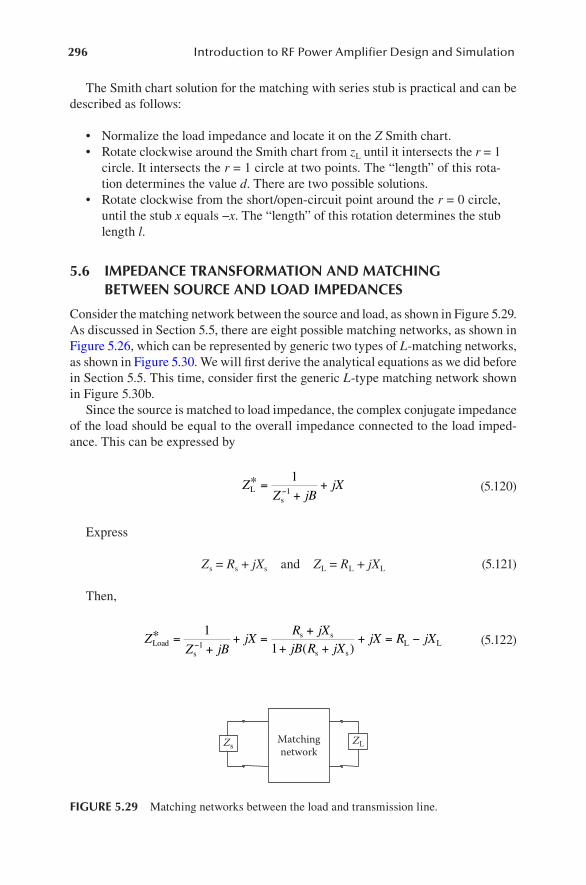
296 Introduction to RF Power Amplifier Design and Simulation
The Smith chart solution for the matching with series stub is practical and can be described as follows:
• Normalize the load impedance and locate it on the Z Smith chart.• Rotate clockwise around the Smith chart from zL until it intersects the r = 1
circle. It intersects the r = 1 circle at two points. The “length” of this rota-tion determines the value d. There are two possible solutions.
• Rotate clockwise from the short/open-circuit point around the r = 0 circle, until the stub x equals −x. The “length” of this rotation determines the stub length l.
5.6 IMPEDANCE TRANSFORMATION AND MATCHING BETWEEN SOURCE AND LOAD IMPEDANCES
Consider the matching network between the source and load, as shown in Figure 5.29. As discussed in Section 5.5, there are eight possible matching networks, as shown in Figure 5.26, which can be represented by generic two types of L-matching networks, as shown in Figure 5.30. We will first derive the analytical equations as we did before in Section 5.5. This time, consider first the generic L-type matching network shown in Figure 5.30b.
Since the source is matched to load impedance, the complex conjugate impedance of the load should be equal to the overall impedance connected to the load imped-ance. This can be expressed by
ZZ jB
jXLs
* =+
+−
11 (5.120)
Express
Zs = Rs + jXs and ZL = RL + jXL (5.121)
Then,
ZZ jB
jXR jXjB R jX
jX R jXLoads
s s
s sL L
*( )
=+
+ =+
+ ++ = −
−
111 (5.122)
ZLZsMatchingnetwork
FIGURE 5.29 Matching networks between the load and transmission line.
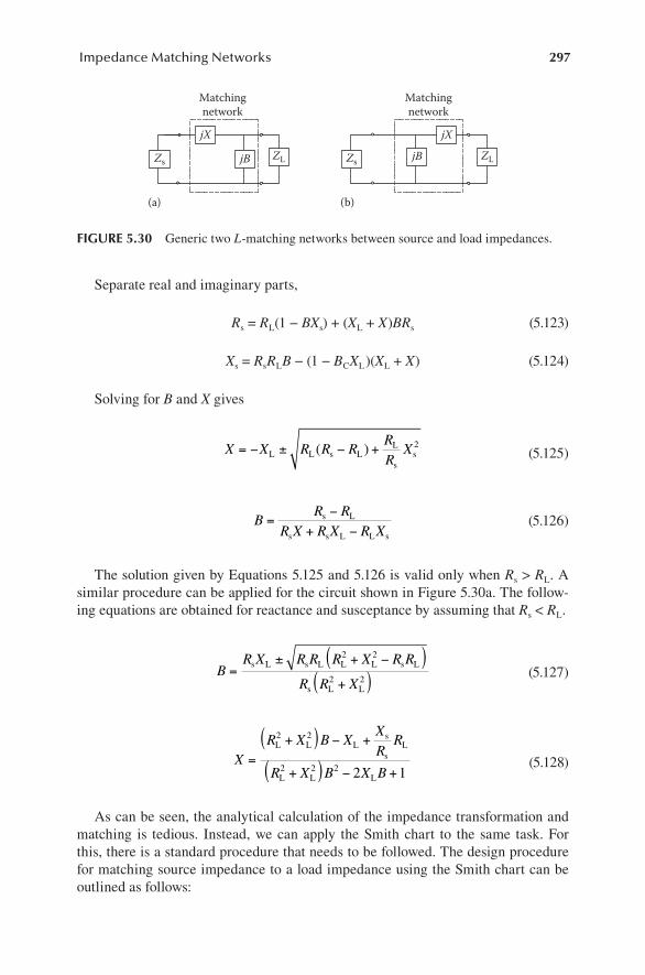
297Impedance Matching Networks
Separate real and imaginary parts,
Rs = RL(1 − BXs) + (XL + X)BRs (5.123)
Xs = RsRLB − (1 − BCXL )(XL + X) (5.124)
Solving for B and X gives
X X R R RRR
X= − ± − +L L s LL
ss( ) 2
(5.125)
BR R
R X R X R X=
−+ −
s L
s s L L s
(5.126)
The solution given by Equations 5.125 and 5.126 is valid only when Rs > RL. A similar procedure can be applied for the circuit shown in Figure 5.30a. The follow-ing equations are obtained for reactance and susceptance by assuming that Rs < RL.
BR X R R R X R R
R R X=
± + −( )+( )
s L s L L L s L
s L L
2 2
2 2 (5.127)
XR X B X
XRR
R X B X B=
+( ) − +
+( ) − +
L L Ls
sL
L L L
2 2
2 2 2 2 1 (5.128)
As can be seen, the analytical calculation of the impedance transformation and matching is tedious. Instead, we can apply the Smith chart to the same task. For this, there is a standard procedure that needs to be followed. The design procedure for matching source impedance to a load impedance using the Smith chart can be outlined as follows:
jX
ZL ZLZsZs
Matchingnetwork
Matchingnetwork
jB jB
jX
(a) (b)
FIGURE 5.30 Generic two L-matching networks between source and load impedances.
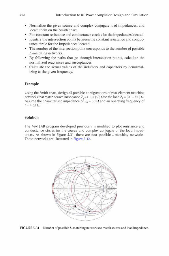
298 Introduction to RF Power Amplifier Design and Simulation
• Normalize the given source and complex conjugate load impedances, and locate them on the Smith chart.
• Plot constant resistance and conductance circles for the impedances located.• Identify the intersection points between the constant resistance and conduc-
tance circle for the impedances located.• The number of the intersection point corresponds to the number of possible
L-matching networks.• By following the paths that go through intersection points, calculate the
normalized reactances and susceptances.• Calculate the actual values of the inductors and capacitors by denormal-
izing at the given frequency.
Example
Using the Smith chart, design all possible configurations of two-element matching networks that match source impedance Zs = (15 + j50) Ω to the load ZL = (20 − j30) Ω. Assume the characteristic impedance of Z0 = 50 Ω and an operating frequency of f = 4 GHz.
Solution
The MATLAB program developed previously is modified to plot resistance and conductance circles for the source and complex conjugate of the load imped-ances. As shown in Figure 5.31, there are four possible L-matching networks. These networks are illustrated in Figure 5.32.
A B
C
zin
zloonJ
D
FIGURE 5.31 Number of possible L-matching networks to match source and load impedance.
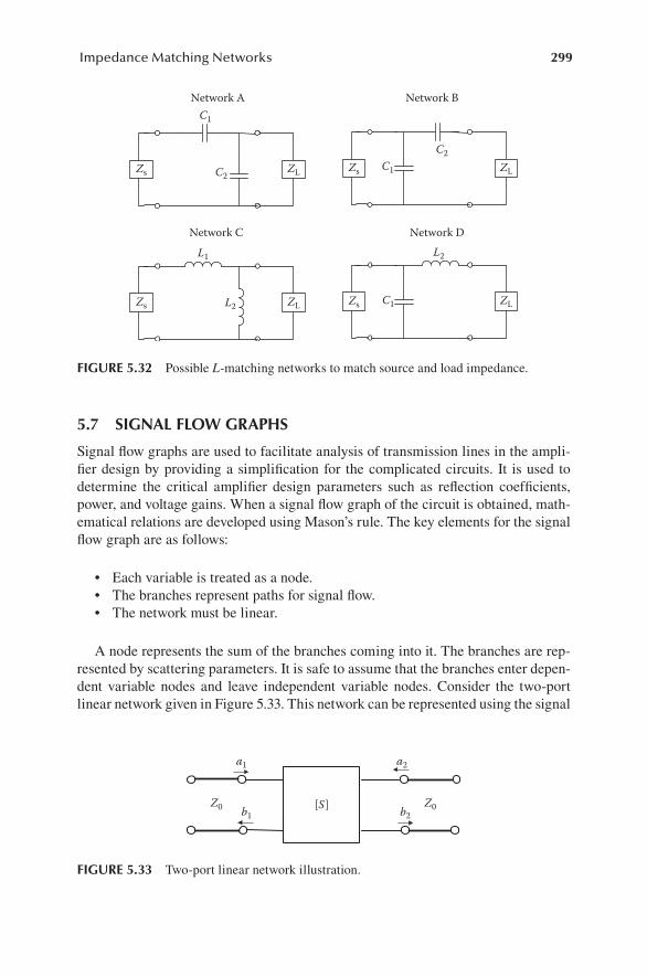
299Impedance Matching Networks
5.7 SIGNAL FLOW GRAPHS
Signal flow graphs are used to facilitate analysis of transmission lines in the ampli-fier design by providing a simplification for the complicated circuits. It is used to determine the critical amplifier design parameters such as reflection coefficients, power, and voltage gains. When a signal flow graph of the circuit is obtained, math-ematical relations are developed using Mason’s rule. The key elements for the signal flow graph are as follows:
• Each variable is treated as a node.• The branches represent paths for signal flow.• The network must be linear.
A node represents the sum of the branches coming into it. The branches are rep-resented by scattering parameters. It is safe to assume that the branches enter depen-dent variable nodes and leave independent variable nodes. Consider the two-port linear network given in Figure 5.33. This network can be represented using the signal
ZL ZL
ZLZL
C1
C2
L2
L2
C1
L1
C2C1Zs
Zs Zs
Zs
Network A Network B
Network C Network D
FIGURE 5.32 Possible L-matching networks to match source and load impedance.
[S ]
a1
b1
a2
b2Z0 Z0
FIGURE 5.33 Two-port linear network illustration.
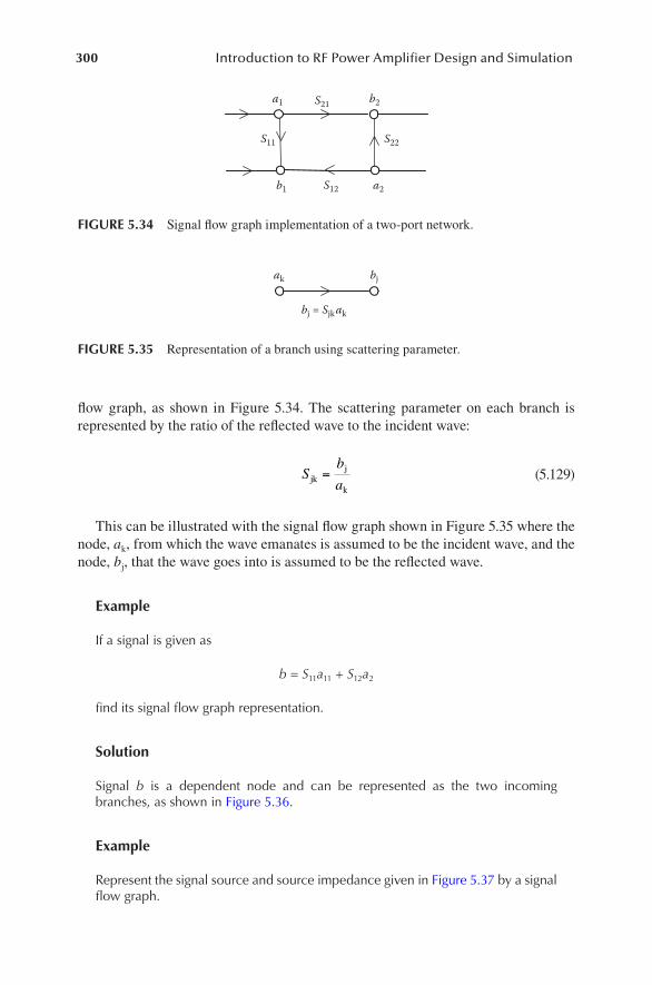
300 Introduction to RF Power Amplifier Design and Simulation
flow graph, as shown in Figure 5.34. The scattering parameter on each branch is represented by the ratio of the reflected wave to the incident wave:
Sb
ajkj
k
= (5.129)
This can be illustrated with the signal flow graph shown in Figure 5.35 where the node, ak, from which the wave emanates is assumed to be the incident wave, and the node, bj, that the wave goes into is assumed to be the reflected wave.
Example
If a signal is given as
b = S11a11 + S12a2
find its signal flow graph representation.
Solution
Signal b is a dependent node and can be represented as the two incoming branches, as shown in Figure 5.36.
Example
Represent the signal source and source impedance given in Figure 5.37 by a signal flow graph.
a1
b1 a2
b2S21
S22
S12
S11
FIGURE 5.34 Signal flow graph implementation of a two-port network.
ak bj
bj = Sjk ak
FIGURE 5.35 Representation of a branch using scattering parameter.
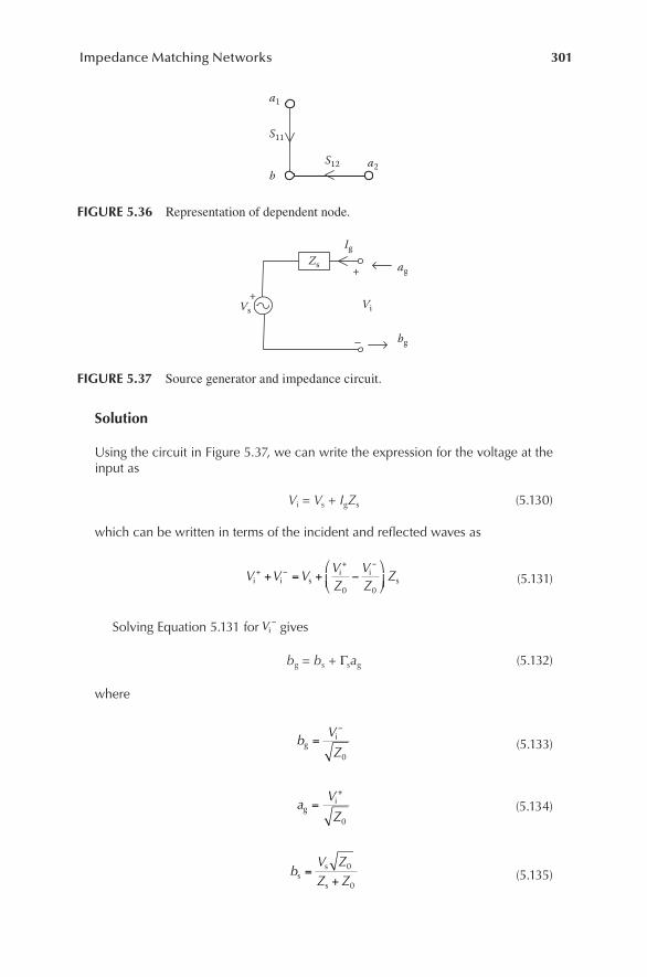
301Impedance Matching Networks
Solution
Using the circuit in Figure 5.37, we can write the expression for the voltage at the input as
Vi = Vs + IgZs (5.130)
which can be written in terms of the incident and reflected waves as
V V VVZ
VZ
Zi i si i
s+ −
+ −
+ = + −
0 0 (5.131)
Solving Equation 5.131 for Vi− gives
bg = bs + Γsag (5.132)
where
bV
Zg
i=−
0 (5.133)
aV
Zg
i=+
0
(5.134)
bV ZZ Zss
s
=+
0
0 (5.135)
S11
a1
a2S12b
FIGURE 5.36 Representation of dependent node.
Vi+
+
–
ag
bg
Vs
Zs
Ig
FIGURE 5.37 Source generator and impedance circuit.
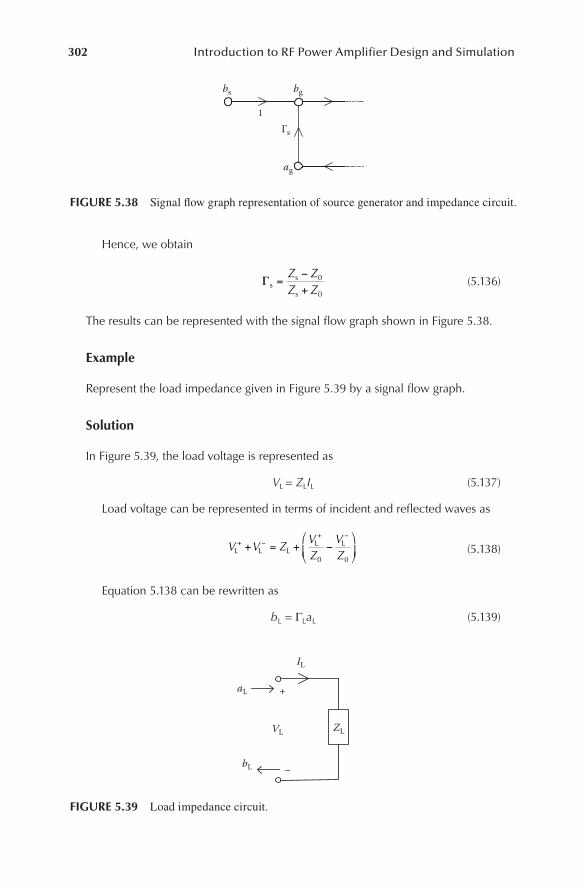
302 Introduction to RF Power Amplifier Design and Simulation
Hence, we obtain
Γss
s
=−+
Z ZZ Z
0
0
(5.136)
The results can be represented with the signal flow graph shown in Figure 5.38.
Example
Represent the load impedance given in Figure 5.39 by a signal flow graph.
Solution
In Figure 5.39, the load voltage is represented as
VL = ZLIL (5.137)
Load voltage can be represented in terms of incident and reflected waves as
V V ZVZ
VZL L L
L L+ −+ −
+ = + −
0 0 (5.138)
Equation 5.138 can be rewritten as
bL = ΓLaL (5.139)
bg
ag
Гs
bs
1
FIGURE 5.38 Signal flow graph representation of source generator and impedance circuit.
VL ZL
IL
+
–
aL
bL
FIGURE 5.39 Load impedance circuit.
303Impedance Matching Networks
where
bV
ZL
L=−
0 (5.140)
aV
ZL
L=+
0 (5.141)
ΓLL
L
=−+
Z ZZ Z
0
0
(5.142)
Using Equation 5.139, we can represent the load impedance in Figure 5.39 with the signal flow graph shown in Figure 5.40.
Example
Represent the two-port transmission circuit shown in Figure 5.38 with the signal flow graph.
Solution
We can now combine the solutions given in Figures 5.38 and 5.40 and obtain the signal flow graph representation for the transmission line circuit shown in Figure 5.41, as illustrated in Figure 5.42.
ГL
bL
aL
FIGURE 5.40 Signal flow graph representation of load impedance.
VLViVsZ0 ZL
+
–
aL
+
+
–
Zs
ag
bg bL
FIGURE 5.41 Transmission line circuit.
304 Introduction to RF Power Amplifier Design and Simulation
PROBLEMS
1. Identify the location of the impedance points given below in the Z Smith chart. Assume that Z0 = 50 Ω.
Z1 = 10 + j5, Z2 = 25 + j15, Y3 = 0.5 + j1, Y4 = 2 + j1.6
2. A 5-m lossless dielectric-spaced transmission line with εr = 2.08 having a characteristic impedance of 50 Ω is terminated with an impedance 50 + j25 (Ω) at an operating frequency of 2 GHz. Find the input impedance.
3. Calculate the following parameters given for the transmission line shown in Figure 5.43 when impedance of 120 + j50 [Ω] is connected.
a. The VSWR on the line b. Load reflection coefficient c. Admittance of the load d. Impedance at the input of the line of the line e. The distance from the load to the first voltage minimum f. The distance from the load to the first voltage maximum 4. Find the input impedance for the circuit shown in Figure 5.44 at 3 GHz
when the load connected is ZL = 75 Ω using the Smith chart. 5. Using the Smith chart, design all possible configurations of two-element
matching networks that match source impedance Zs = (25 + j70) Ω to the load ZL = (10 − j10) Ω. Assume the characteristic impedance of Z0 = 50 Ω and an operating frequency of f = 2 GHz.
6. Using the ZY Smith chart, find the input impedance of the circuit in Figure 5.45 at 3 GHz and 5 GHz.
bs bg
ag
Гs ГL
aL
bL
1
FIGURE 5.42 Signal flow graph representation of transmission line circuit.
Zin
l = 0.25λ
Z0 = 50 [Ω] ZL = 120 + j50 [Ω]
FIGURE 5.43 Transmission line circuit.
305Impedance Matching Networks
REFERENCE
1. A. Eroglu. 2013. RF Circuit Design Techniques for MF-UHF Applications. CRC Press, Boca Raton, FL.
Zin R = 75 [Ω]C = 2.5 [pF]
L = 4 [nH]
FIGURE 5.44 Impedance transformation.
Zin C1 L3
L1 L2C2 R
25 Ω1.59 pF3.98 nH1.99 nH
3.98 nH1.68 nH
FIGURE 5.45 Input impedance using ZY Smith chart.

307
6 Couplers, Multistate Reflectometers, and RF Power Sensors for Amplifiers
6.1 INTRODUCTION
Radio frequency (RF) power amplifiers have several subsystems and surrounding passive components that include directional couplers, combiners/splitters, imped-ance, and phase measurement devices such as reflectometers and RF sensors, as shown in Figure 6.1. The complete RF system will only work if all of its subcompo-nents are designed and interfaced based on the operational requirements. The inte-gration of the subcomponents and assemblies in practice has been done by system engineers in coordination with RF design engineers. In this chapter, the design meth-ods for couplers and reflectometers and RF power sensors will be given.
6.2 DIRECTIONAL COUPLERS
Directional couplers are a critical device in RF amplifiers and used widely as a sam-pling device for measuring forward and reflected power based on the magnitude of the reflection coefficient. Directional couplers can be implemented as a planar device using transmission lines such as microstrip and stripline or lumped elements with transformers based on the frequency of operation. Conventional directional couplers are four-port devices consisting of main and coupled lines, as shown in Figure 6.2 [1].
Under the matched conditions, when the device is assumed to be lossless, the fol-lowing relations are valid:
S11 = S22 = S33 = S44 = 0 (6.1)
S†S = I (6.2)
where † is used for the conjugate transpose of the matrix, and I represents the unit matrix. From Equation 6.2,
S S S14 13
2
24
20* −( ) = (6.3)
308In
trod
uctio
n to
RF Po
wer A
mp
lifier D
esign an
d Sim
ulatio
n
RFoutput
Systemcontroller
Modulator
RF amplifier chain
T
Powersupplies
Splitter Combiner
Compensator and processcontroller
EMIfilter
Cctbrkr
3phAC in
Filter Impedance andphase probe
Predriver Driver
Temperaturesensing Main amplifier
FIGURE 6.1 RF amplifier with its surrounding subsystems.

309Couplers, Reflectometers, and RF Power Sensors for Amplifiers
S S S23 12
2
34
20−( ) = (6.4)
If the network is assumed to be a symmetrical device, then
S14 = S41 = S23 = S32 = 0 (6.5)
Hence,
S S12
2
13
21+ = (6.6)
S S12
2
24
21+ = (6.7)
S S13
2
34
21+ = (6.8)
S S24
2
34
21+ = (6.9)
which lead to
S S S S13 24 12 34= =, (6.10)
As a result, the scattering matrix for symmetrical, lossless directional coupler can be obtained as
S
j
j
j
j
=
0 0
0 0
0 0
0 0
α β
α β
β α
β α
(6.11)
Input portλ/4
Coupled port
Output port
Isolated port
Main lineCoupled line
P1
P3
P2
P4
FIGURE 6.2 Directional coupler as a four-port device.
310 Introduction to RF Power Amplifier Design and Simulation
where
S12 = S34 = α, (6.12)
S13 = S24 = jβ (6.13)
Important directional coupler performance parameters, i.e., the coupling level, isolation level, and directivity level, can be found from
Coupling level (dB) =
= −10 201
3
log log( )PP
β (6.14)
Isolation level (dB) =
= − (10 201
414log log
PP
S )) (6.15)
Directivity level (dB) =
=10 203
4 1
log logPP S
β
44
(6.16)
6.2.1 Microstrip Directional couplers
The design of microstrip directional couplers has been discussed in Refs. [1–3]. In this section, two-line, three-line, and multilayer planar directional coupler designs will be discussed.
6.2.1.1 Two-Line Microstrip Directional CouplersConsider the geometry of a symmetrical microstrip directional coupler as shown in Figure 6.3.
ww
hεr
s
FIGURE 6.3 Symmetrical two-line microstrip directional coupler.
311Couplers, Reflectometers, and RF Power Sensors for Amplifiers
In practice, port termination impedances, coupling level, and operational fre-quency are input design parameters that are being used to realize couplers. The matched system is accomplished when the characteristic impedance,
Z Z Zo oe oo= (6.17)
is equal to the port impedance. In Equation 6.17, Zoe and Zoo are the even- and odd-mode impedances, respectively. The even and odd impedances, Zoe and Zoo, of the microstrip coupler given in Figure 6.3 can be found from
Z ZC
Coe =+
−0
20
20
1 10
1 10
/
/ (6.18)
Z ZC
Coo =−
+0
20
20
1 10
1 10
/
/ (6.19)
where C is the forward coupling requirement and given in decibels. The physical dimen-sions of the directional coupler are found using the synthesis method. Application of the synthesis method gives the spacing ratio s/h of the coupler in Figure 6.3 as
s h
wh
wh
/ se=
+
−2 2 21
π
π π
cosh
cosh cosh
′
−
′
−
so
so
2
2cosh cos
π wh
hhπ2
wh
se
(6.20)
(w/h)se and (w/h)so are the shape ratios for the equivalent single case corresponding to even-mode and odd-mode geometry, respectively. ( )w h/ so′ is the second term for the shape ratio. (w/h) is the shape ratio for the single microstrip line, and it is expressed as
wh
R
=
+
−
++
+8
42 41 1
7 411
1 1exp
.( )
( ) (ε
εr
r/ // r
r
ε
ε
).
exp.
0 81
42 41 1
R+
−
(6.21)
where
RZ
RZ
= =oe ooor2 2
(6.22)

312 Introduction to RF Power Amplifier Design and Simulation
Zose and Zoso are the characteristic impedances corresponding to single microstrip shape ratios (w/h)se and (w/h)so, respectively. They are given as
ZZ
oseoe=2
(6.23)
ZZ
osooo=2
(6.24)
and
( ) ( )w h w hR Z
/ /seose
==
(6.25)
( ) ( )w h w hR Z
/ /sooso
==
(6.26)
The term ( )w h/ so′ in Equation 6.20 is given as
wh
wh
wh
′=
+
so so se
0 78 0 1. . (6.27)
After the spacing ratio s/h for the coupled lines is found, we can proceed to find w/h for the coupled lines. The shape ratio for the coupled lines is
wh
dsh
= −
−1 1
21
πcosh ( ) (6.28)
where
d
wh
g g
=
+ + −cosh ( )π2
1 1
2se
(6.29)
gsh
=
cosh
π2 (6.30)
The physical length of the directional coupler is obtained using
lc
f= =λ
ε4 4 eff
(6.31)
313Couplers, Reflectometers, and RF Power Sensors for Amplifiers
where c = 3 × 10⁸ m/s, and f is the operational frequency in hertz. Hence, the length of the directional coupler can be found if the effective permittivity constant εeff of the coupled structure shown in Figure 6.1 is known. εeff can be found from
εε ε
effeffe effo=
+
2
2
(6.32)
εeffe and εeffo are the effective permittivity constants of the coupled structure for odd and even modes, respectively. εeffe and εeffo depend on even- and odd-mode capacitances Ce and Co as
εeffee
e1
=CC
(6.33)
εeffoo
o
=CC 1
(6.34)
Ce1,o1 is the capacitance with air as dielectric. All the capacitances are given as capacitance per unit length. The even-mode capacitance Ce is
C C C Ce p f f= + + ′ (6.35)
The capacitances in the even mode for the coupled lines can be visualized as shown in Figure 6.4.
+ + +
+ + + – – –
+ + +
Cf
Cf Cf
CgdCgd
CgaCga
Cp Cp
CfC f C fCp Cp
Magnetic wall
Electric wall
(a)
(b)
FIGURE 6.4 Coupled line mode representation: (a) even mode; (b) odd mode.

314 Introduction to RF Power Amplifier Design and Simulation
Cp is the parallel plate capacitance and is defined as
Cwhp r= ε ε0 (6.36)
where w/h is found in Section 6.1. Cf is the fringing capacitance due to the microstrip being taken alone as if it were a single strip. That is equal to
CcZ
Cf
seff p= −ε
2 20 (6.37)
Here, εseff is the effective permittivity constant of a single-strip microstrip. It can be expressed as
εε ε
seffr r /=+
−−1
21
2F w h( ) (6.38)
where
F w h
h w w hw
h( )
( ) . ( )/
/
/ / for
=
+ + − ≤
−1 12 0 041 1 11 2 2
(( ) /1 12 11 2+ ≥
−h ww
h/ for
(6.39)
′Cf is given by the following equation:
′ =
+
C
C
Ahs
sh
ff r
seff110
1 4
tanh
/εε
(6.40)
and
Awh
= − −
exp . exp . .0 1 2 33 1 5 (6.41)
The odd-mode capacitance Co is
Co = Cp + Cf + Cga + Cgd (6.42)
The capacitances in the odd mode for the coupled lines can be visualized as shown in Figure 6.4. Cga is the capacitance term in the odd mode for the fringing field across the gap in the air region. It can be written as
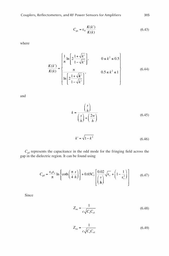
315Couplers, Reflectometers, and RF Power Sensors for Amplifiers
C
K kK kga =
′ε0
( )( )
(6.43)
where
K kK k
k
kk
( )( )
ln , .
ln
′=
+ ′
− ′
≤ ≤
+ ′
121
10 5
21
π
π
0 2
kk
k
k
1
1
− ′
≤ ≤
, 0.5 2
(6.44)
and
k
sh
sh
wh
=
+2
(6.45)
′ = −k k1 2 (6.46)
Cgd represents the capacitance in the odd mode for the fringing field across the gap in the dielectric region. It can be found using
Csh
Cs
gdr
f=
+
ε επ
π0
40 65
0 02ln coth .
.
hh
+ −
εε
rr
112 (6.47)
Since
Zc C C
oe
e e
=1
1
(6.48)
Zc C C
oo
o o
=1
1
(6.49)
316 Introduction to RF Power Amplifier Design and Simulation
then we can write
Cc C Z
ee oe
1 2 2
1= (6.50)
Cc C Z
oo oo
1 2 2
1= (6.51)
Substituting Equations 6.32, 6.35, 6.40, and 6.51 into Equations 6.34 and 6.35 gives the even- and odd-mode effective permittivities εeffe and εeffo. When Equations 6.34 and 6.35 are substituted into Equation 6.33, we can find the effective permittiv-ity constant εeff of the coupled structure. Now, Equation 6.31 can be used to calcu-late the physical length of the directional coupler at the operational frequency. The design tables to design two-line microstrip couplers with various commonly used RF materials and several application examples are given in Ref. [1].
6.2.1.2 Three-Line Microstrip Directional CouplersThree-line, six-port microstrip directional couplers can be used for several pur-poses in RF applications including voltage, current, impedance, and voltage stand-ing wave ratio (VSWR) measurements. As a result, six-port microstrip directional couplers are cost-effective alternatives to existing reflectometers. The design and performance of six-port reflectometers based on microstrip-type couplers have been analyzed and given in Ref. [4]. The method described in Refs. [1,2] gives the complete design method of two-line symmetrical directional couplers with closed-form relations using the synthesis technique, as described in Section 6.2.1.1. The method used in Refs. [1,2] reflects the design practice since the physical dimen-sions of the coupler are not known prior to the design of the coupler. Their design procedure requires only the knowledge of port impedances, the desired coupling level, and the operational frequency. The physical dimensions of the coupler including the width of the trace, the spacing between them, and the thickness of the dielectric substrate are then determined using the closed relations based on the given three design requirements.
Three-line, six-port directional couplers shown in Figure 6.5 give cost-effective alternatives to existing reflectometers and can be used for diagnostic purposes. There are some analytical formulations to design the six-port couplers, which are given in Refs. [4–7], but none of them in the literature uses the practical approach for two-line coupler design, which reflects the engineering practice outlined in Section 6.1.
In this section, we present closed-form relations to design three-line microstrip directional couplers using the method implemented in practice. The design method given here again requires knowledge of only coupling level, port impedances, and operational frequency. A three-step design procedure with accurate closed formulas is given to have a complete design of symmetrical three-line microstrip directional couplers at the desired operational frequency. The physical dimensions of the cou-pler including the physical length are obtained with the method presented, and the
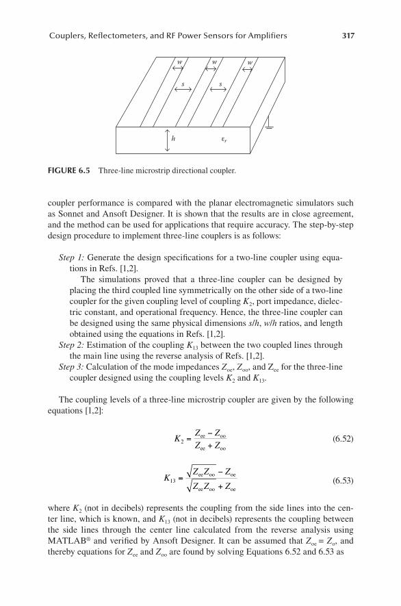
317Couplers, Reflectometers, and RF Power Sensors for Amplifiers
coupler performance is compared with the planar electromagnetic simulators such as Sonnet and Ansoft Designer. It is shown that the results are in close agreement, and the method can be used for applications that require accuracy. The step-by-step design procedure to implement three-line couplers is as follows:
Step 1: Generate the design specifications for a two-line coupler using equa-tions in Refs. [1,2].
The simulations proved that a three-line coupler can be designed by placing the third coupled line symmetrically on the other side of a two-line coupler for the given coupling level of coupling K2, port impedance, dielec-tric constant, and operational frequency. Hence, the three-line coupler can be designed using the same physical dimensions s/h, w/h ratios, and length obtained using the equations in Refs. [1,2].
Step 2: Estimation of the coupling K13 between the two coupled lines through the main line using the reverse analysis of Refs. [1,2].
Step 3: Calculation of the mode impedances Zoe, Zoo, and Zee for the three-line coupler designed using the coupling levels K2 and K13.
The coupling levels of a three-line microstrip coupler are given by the following equations [1,2]:
KZ ZZ Z2 =
−+
ee oo
ee oo
(6.52)
KZ Z Z
Z Z Z13 =
−
+ee oo oe
ee oo oe (6.53)
where K2 (not in decibels) represents the coupling from the side lines into the cen-ter line, which is known, and K13 (not in decibels) represents the coupling between the side lines through the center line calculated from the reverse analysis using MATLAB® and verified by Ansoft Designer. It can be assumed that Zoe = Zo, and thereby equations for Zee and Zoo are found by solving Equations 6.52 and 6.53 as
ss
w w w
h εr
FIGURE 6.5 Three-line microstrip directional coupler.
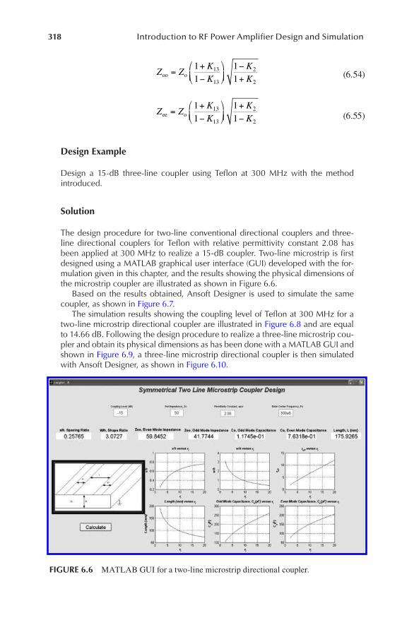
318 Introduction to RF Power Amplifier Design and Simulation
Z ZKK
KKoo o=
+−
−+
11
11
13
13
2
2 (6.54)
Z ZKK
KKee o=
+−
+−
11
11
13
13
2
2 (6.55)
Design Example
Design a 15-dB three-line coupler using Teflon at 300 MHz with the method introduced.
Solution
The design procedure for two-line conventional directional couplers and three-line directional couplers for Teflon with relative permittivity constant 2.08 has been applied at 300 MHz to realize a 15-dB coupler. Two-line microstrip is first designed using a MATLAB graphical user interface (GUI) developed with the for-mulation given in this chapter, and the results showing the physical dimensions of the microstrip coupler are illustrated as shown in Figure 6.6.
Based on the results obtained, Ansoft Designer is used to simulate the same coupler, as shown in Figure 6.7.
The simulation results showing the coupling level of Teflon at 300 MHz for a two-line microstrip directional coupler are illustrated in Figure 6.8 and are equal to 14.66 dB. Following the design procedure to realize a three-line microstrip cou-pler and obtain its physical dimensions as has been done with a MATLAB GUI and shown in Figure 6.9, a three-line microstrip directional coupler is then simulated with Ansoft Designer, as shown in Figure 6.10.
FIGURE 6.6 MATLAB GUI for a two-line microstrip directional coupler.
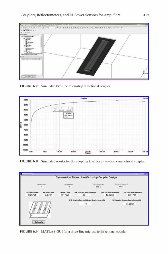
319Couplers, Reflectometers, and RF Power Sensors for Amplifiers
FIGURE 6.7 Simulated two-line microstrip directional coupler.
FIGURE 6.8 Simulated results for the coupling level for a two-line symmetrical coupler.
FIGURE 6.9 MATLAB GUI for a three-line microstrip directional coupler.
http://www.crcnetbase.com/action/showImage?doi=10.1201/b18677-7&iName=master.img-001.jpg&w=335&h=145

320 Introduction to RF Power Amplifier Design and Simulation
The simulation results showing the coupling level between the main line and coupled line for Teflon at 300 MHz for a three-line microstrip directional coupler are illustrated in Figure 6.11 and are equal to 16.1397 dB. Hence, the given closed-form relations and design procedure can be successfully designed to implement three-line microstrip directional couplers.
6.2.2 Multilayer planar Directional couplers
In this section, the design of multilayer microstrip two-line and three-line directional couplers is given. A step-by-step design procedure reflecting the design practice of directional couplers, which requires only information on coupling level, port imped-ances, and operational frequency, is given. The method based on the synthesis tech-nique applied in the design of two-line microstrip symmetrical directional couplers by Eroglu [1,2] is adapted to design multilayer directional couplers with the aid of electromagnetic simulators and curve fitting. The proposed design method is com-pared with the existing measurement results, and the accuracy is verified. It also has
FIGURE 6.10 Simulated three-line microstrip directional coupler.
FIGURE 6.11 Simulated results for the coupling level for a two-line symmetrical coupler.
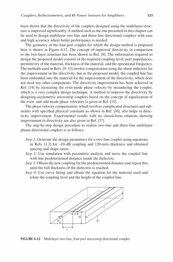
321Couplers, Reflectometers, and RF Power Sensors for Amplifiers
been shown that the directivity of the couplers designed using the multilayer struc-ture is improved significantly. A method such as the one presented in this chapter can be used to design multilayer two-line and three-line directional couplers with ease and high accuracy where better performance is needed.
The geometry of the four-port coupler for which the design method is proposed here is shown in Figure 6.12. The concept of improved directivity in comparison to the two-layer structure has been shown in Ref. [8]. The information required to design the proposed model consists of the required coupling level, port impedances, permittivity of the material, thickness of the material, and the operational frequency. The methods used in Refs. [9–13] involve compensation using the shunt inductors for the improvement in the directivity, but in the proposed model, the coupled line has been embedded into the material for the improvement of the directivity, which does not need any other components. The directivity improvement has been achieved in Ref. [14] by increasing the even-mode phase velocity by meandering the coupler, which is a very complex design technique. A method to improve the directivity by designing asymmetric microstrip couplers based on the concept of equalization of the even- and odd-mode phase velocities is given in Ref. [15].
The phase velocity compensation, which involves complicated structures and sub-strates with specified physical constants as shown in Ref. [16], also helps in direc-tivity improvement. Experimental results with no closed-form relations showing improvement in directivity are also given in Ref. [17].
The step-by-step design procedure to realize two-line and three-line multilayer planar directional couplers is as follows:
Step 1: Generate the design parameters for a two-line coupler using equations in Refs. [1,2] for −10-dB coupling and 120-mils thickness and obtained spacing and shape ratios.
Step 2: Use simulation with parametric analysis and move the coupled line with fine predetermined distance inside the dielectric.
Step 3: Obtain the new coupling for the predetermined distance and repeat this until the full thickness of the dielectric is reached.
Step 4: Use curve fitting and obtain the equation for the material used and relate the coupling level and the height of the coupled line.
h
s
Hw
l
FIGURE 6.12 Multilayer two-line, four-port microstrip directional coupler.

322 Introduction to RF Power Amplifier Design and Simulation
Design Example
Design a 15-dB two-line, multilayer directional coupler using FR4 at 300 MHz with the method introduced. Compare the directivity of the results for the multilayer direc-tional coupler with the directivity of the conventional two-line directional coupler.
Solution
The design procedure begins with finding the physical dimension of the con-ventional two-line microstrip directional coupler with the method introduced in Refs. [1,2]. A MATLAB GUI has been developed to design any multilayer two-line directional coupler, as shown in Figure 6.13.
The multilayer directional coupler is then implemented using Ansoft Designer, as shown in Figure 6.14.
FIGURE 6.13 MATLAB GUI for multilayer two-line, four-port microstrip directional coupler.
FIGURE 6.14 Simulated three-line, multilayer planar directional coupler.
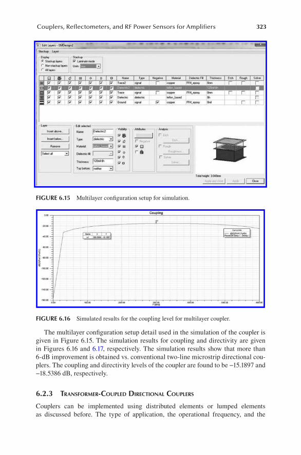
323Couplers, Reflectometers, and RF Power Sensors for Amplifiers
The multilayer configuration setup detail used in the simulation of the coupler is given in Figure 6.15. The simulation results for coupling and directivity are given in Figures 6.16 and 6.17, respectively. The simulation results show that more than 6-dB improvement is obtained vs. conventional two-line microstrip directional cou-plers. The coupling and directivity levels of the coupler are found to be −15.1897 and −18.5386 dB, respectively.
6.2.3 transforMer-coupleD Directional couplers
Couplers can be implemented using distributed elements or lumped elements as discussed before. The type of application, the operational frequency, and the
FIGURE 6.15 Multilayer configuration setup for simulation.
FIGURE 6.16 Simulated results for the coupling level for multilayer coupler.
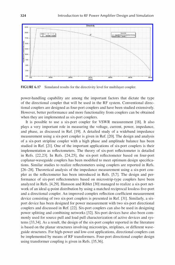
324 Introduction to RF Power Amplifier Design and Simulation
power-handling capability are among the important factors that dictate the type of the directional coupler that will be used in the RF system. Conventional direc-tional couplers are designed as four-port couplers and have been studied extensively. However, better performance and more functionality from couplers can be obtained when they are implemented as six-port couplers.
It is possible to use a six-port coupler for VSWR measurement [18]. It also plays a very important role in measuring the voltage, current, power, impedance, and phase, as discussed in Ref. [19]. A detailed study of a wideband impedance measurement using a six-port coupler is given in Ref. [20]. The design and analysis of a six-port stripline coupler with a high phase and amplitude balance has been studied in Ref. [21]. One of the important applications of six-port couplers is their implementation as reflectometers. The theory of six-port reflectometer is detailed in Refs. [22,23]. In Refs. [24,25], the six-port reflectometer based on four-port coplanar-waveguide couplers has been modified to meet optimum design specifica-tions. Similar studies to realize reflectometers using couplers are reported in Refs. [26–28]. Theoretical analysis of the impedance measurement using a six-port cou-pler as the reflectometer has been introduced in Refs. [5,7]. The design and per-formance of six-port reflectometers based on microstrip-type couplers have been analyzed in Refs. [4,29]. Hansson and Riblet [30] managed to realize a six-port net-work of an ideal q-point distribution by using a matched reciprocal lossless five-port and a directional coupler. An improved complex reflection coefficient measurement device consisting of two six-port couplers is presented in Ref. [31]. Similarly, a six-port device has been designed for power measurement with two six-port directional couplers and discussed in Ref. [22]. Six-port couplers can also be used in designing power splitting and combining networks [32]. Six-port devices have also been com-monly used for source pull and load pull characterization of active devices and sys-tems [33,34]. As a result, the design of the six-port coupler reported in the literature is based on the planar structures involving microstrips, striplines, or different wave-guide structures. For high-power and low-cost applications, directional couplers can be implemented by means of RF transformers. Four-port directional coupler design using transformer coupling is given in Refs. [35,36].
FIGURE 6.17 Simulated results for the directivity level for multilayer coupler.
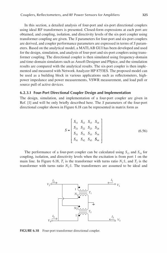
325Couplers, Reflectometers, and RF Power Sensors for Amplifiers
In this section, a detailed analysis of four-port and six-port directional couplers using ideal RF transformers is presented. Closed-form expressions at each port are obtained, and coupling, isolation, and directivity levels of the six-port coupler using transformer coupling are given. The S parameters for four-port and six-port couplers are derived, and coupler performance parameters are expressed in terms of S param-eters. Based on the analytical model, a MATLAB GUI has been developed and used for the design, simulation, and analysis of four-port and six-port couplers using trans-former coupling. The directional coupler is then simulated using frequency-domain and time-domain simulators such as Ansoft Designer and PSpice, and the simulation results are compared with the analytical results. The six-port coupler is then imple-mented and measured with Network Analyzer HP 8753ES. The proposed model can be used as a building block in various applications such as reflectometers, high-power impedance and power measurements, VSWR measurement, and load pull or source pull of active devices.
6.2.3.1 Four-Port Directional Coupler Design and ImplementationThe design, simulation, and implementation of a four-port coupler are given in Ref. [1] and will be only briefly described here. The S parameters of the four-port directional coupler shown in Figure 6.18 can be represented in matrix form as
S
S S S S
S S S S
S S S S
S S S
=
11 12 13 14
21 22 23 24
31 31 33 34
41 42 43 SS44
(6.56)
The performance of a four-port coupler can be calculated using S13 and S14 for coupling, isolation, and directivity levels when the excitation is from port 1 on the main line. In Figure 6.18, T1 is the transformer with turns ratio N1:1, and T2 is the transformer with turns ratio N2:1. The transformers are assumed to be ideal and
I1
N1
1V1V2
V3V4
I2
I4 I3
N2
1
T1
T2
FIGURE 6.18 Four-port transformer directional coupler.

326 Introduction to RF Power Amplifier Design and Simulation
lossless. The relations between voltages and currents through turn ratios of the direc-tional coupler at the ports can be obtained as
V2 = N2(V4 − V3) (6.57)
V4 = N1(V2 − V1) (6.58)
and
I1 = N1(I3 + I4) (6.59)
I3 = N1(I1 + I2) (6.60)
The scattering parameters of the coupler can be obtained by using the incident and reflected waves, which are designated by ai and bi. Then, the voltages and cur-rents can be expressed in terms of waves as
V Z a bi i i= +( ) (6.61)
IZ
a bi i i= −1
( ) (6.62)
Z is the characteristic impedance at the ports of the directional coupler. The scat-tering parameters of the coupler are obtained by relating the incident and reflected waves using
Sba
a kk
iji
j for j
== ≠0
(6.63)
The scattering parameters that are required to calculate the coupler performance parameters are
SN N N N
N N N N13
1 2 1 2
12
22
12
22
2
4 1=
− +
+ + −( )( )( )( )
(6.64)
SN N N N
N N N N14
1 1 2 22
12
22
12
22
2 1
4 1=
− − + +( )+ + −( )( )
( ) (6.65)
The coupling, isolation, and directivity levels of a four-port coupler are then expressed using S parameters in Section 6.2. Equations 6.64 and 6.65 lead to direc-tional coupler performance parameter calculations through knowledge of only turns
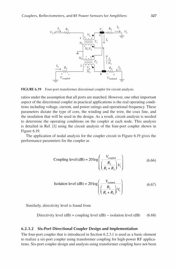
327Couplers, Reflectometers, and RF Power Sensors for Amplifiers
ratios under the assumption that all ports are matched. However, one other important aspect of the directional coupler in practical applications is the real operating condi-tions including voltage, current, and power ratings and operational frequency. These parameters dictate the type of core, the winding and the wire, the coax line, and the insulation that will be used in the design. As a result, circuit analysis is needed to determine the operating conditions on the coupler at each node. This analysis is detailed in Ref. [1] using the circuit analysis of the four-port coupler shown in Figure 6.19.
The application of nodal analysis for the coupler circuit in Figure 6.19 gives the performance parameters for the coupler as
Coupling level dB coupled( ) log=
+
202
1 21
V
RR R
V (6.66)
Isolation level (dB) isolated=
+
202
1 2
logV
RR R
V1
(6.67)
Similarly, directivity level is found from
Directivity level (dB) = coupling level (dB) − isolation level (dB) (6.68)
6.2.3.2 Six-Port Directional Coupler Design and ImplementationThe four-port coupler that is introduced in Section 6.2.3.1 is used as a basic element to realize a six-port coupler using transformer coupling for high-power RF applica-tions. Six-port coupler design and analysis using transformer coupling have not been
I1
N1
1
V1 V2
I2
I4I3
N2
1
T1
T2
R1 R2
R3 R4
+ –VL
N1VL+ –
+–
VoN2
+–
Vo
Is
+ –Vcoupled Visolated
+–
I1N1
a
b
FIGURE 6.19 Four-port transformer directional coupler for circuit analysis.
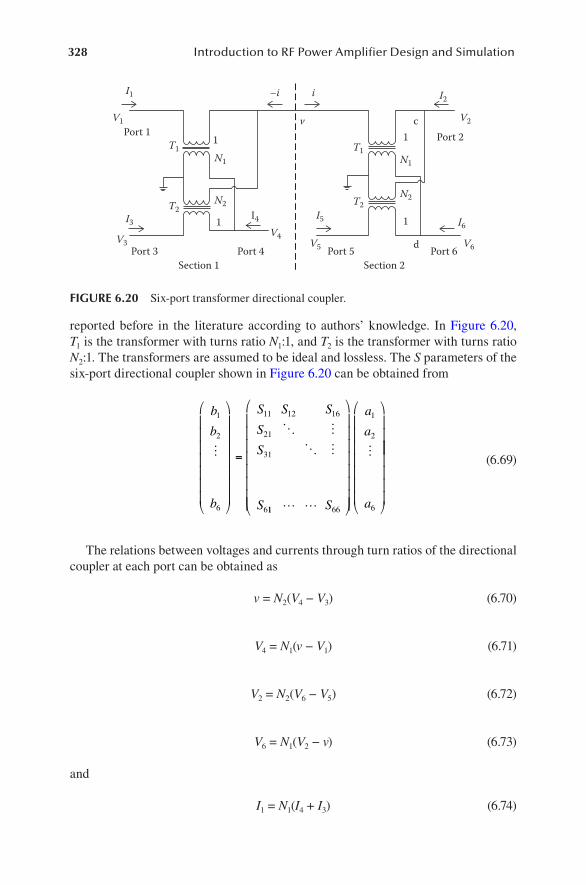
328 Introduction to RF Power Amplifier Design and Simulation
reported before in the literature according to authors’ knowledge. In Figure 6.20, T1 is the transformer with turns ratio N1:1, and T2 is the transformer with turns ratio N2:1. The transformers are assumed to be ideal and lossless. The S parameters of the six-port directional coupler shown in Figure 6.20 can be obtained from
b
b
b
S S S
S
S
S
1
2
6
11 12 16
21
31
6
=
11 66
1
2
6S
a
a
a
(6.69)
The relations between voltages and currents through turn ratios of the directional coupler at each port can be obtained as
v = N2(V4 − V3) (6.70)
V4 = N1(v − V1) (6.71)
V2 = N2(V6 − V5) (6.72)
V6 = N1(V2 − v) (6.73)
and
I1 = N1(I4 + I3) (6.74)
I1
I3 I4 I5 I6
V1Port 1
Port 3 Port 4 Port 5 Port 6
Port 2
Section 2Section 1
v c
dV3V4
V5 V6
V2
1
1
1
1
T1 T1
T2T2
N1
N2N2
N1
I2i–i
FIGURE 6.20 Six-port transformer directional coupler.
329Couplers, Reflectometers, and RF Power Sensors for Amplifiers
I3 = N2(−i + I1) (6.75)
i = N1(I5 + I6) (6.76)
I5 = N2(I2 + i) (6.77)
Then, the voltages and currents are expressed in terms of waves using relations 6.61 and 6.62, and the scattering parameters for coupler performance are then obtained with application of Equation 6.63 as
S S
N N N N N N N N N N62 31
14
23
13
24
13
22
12
23
12
24 4 2 2 2= =
− − + − −(( )+ − − + +8 4 8 2 4 101
424
14
22
13
23
13
2 12
24
12N N N N N N N N N N N NN N N N N N N2
212
22
1 23
1 22 4 1+ + − − + (6.78)
S S
N N N N N N N N
N N42 51
14
23
13
24
13
22
12
23
14
4 4 2 2
8= =
− − + +( )224
14
22
13
23
13
2 12
24
12
22
124 8 2 4 10+ − − + + +N N N N N N N N N N N ++ − − +N N N N N2
21 2
31 22 4 1
(6.79)
S S
N N N N N N N N N N52 41
14
23
13
24
13
22
12
23
12
24 4 10 2 6= =
− − + + −− −( )+ − − +
2 2
8 4 8 2 41 2
21
14
24
14
22
13
23
13
2
N N N
N N N N N N N N N112
24
12
22
12
22
1 23
1 210 2 4 1N N N N N N N N N+ + + − − + (6.80)
S S
N N N N N N N N N N32 61
14
23
13
24
13
22
12
23
12
24 4 6 2 2= =
− − + +( ))+ − − + +8 4 8 2 4 101
424
14
22
13
23
13
2 12
24
12N N N N N N N N N N N N22
212
22
1 23
1 22 4 1+ + − − +N N N N N N (6.81)
The coupling and isolation levels of the six-port directional coupler when operating in forward and reverse modes are then expressed using S parameters as
First coupling level (port 3) = 20 log (−S13) dB (6.82)
Second coupling level (port 5) = 20 log (−S15) dB (6.83)
First isolation level (port 4) = 20 log (−S14) dB (6.84)
Second isolation level (port 6) = 20 log (−S16) dB (6.85)
The directivity level can be obtained again from Equation 6.78 accordingly. Equations 6.78 through 6.85 with Equation 6.78 lead to directional coupler perfor-mance parameter calculations through knowledge of only turns ratios under the assumption that all ports are matched. The real operating conditions require a six-port directional coupler to be analyzed with circuit analysis techniques. The com-plete analysis of the six-port coupler has been performed using forward and reverse modes for the circuit shown in Figures 6.21 and 6.22, respectively.
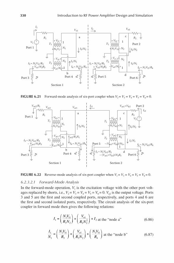
330 Introduction to RF Power Amplifier Design and Simulation
6.2.3.2.1 Forward-Mode AnalysisIn the forward-mode operation, V1 is the excitation voltage with the other port volt-ages replaced by shorts, i.e., V2 = V3 = V4 = V5 = V6 = 0. Vo2 is the output voltage. Ports 3 and 5 are the first and second coupled ports, respectively, and ports 4 and 6 are the first and second isolated ports, respectively. The circuit analysis of the six-port coupler in forward mode then gives the following relations:
IN VR N
V
R NI1
1 1
3 2
1
3 22 2= + +l o
at the “node a” (6.86)
IN
N VR
VR N
N VR
1
1
1 1
3
1
3 2
1 1
4
= + +l o l at the “node b” (6.87)
Section 1
Port 1
Port 3 Port 4 Port 5 Port 6
Port 2
Section 2
aR1+–V1 T1
T2
T1
T2
N1
+ VI1 –
+ N1VI –
– Vo1/N2 +
– Va1 +
+ VI2 –
+ N1V12 –
– Vo2/N2 +
– Vo 2 +N2
N2
N2
I1Vo1
Vo2I2
I3/N2 I5/N2
I2/N1I6 = N1VI2/R6I4 = N1VI1/R4
I3 = N1VI1/R3 + Vo1/N2R3
I5 = N1VI2/R5 + Vo2/N2R5
I1/N1
R3
R6R 5R 4
R2c
db
1
1 1
1
FIGURE 6.21 Forward-mode analysis of six-port coupler when V2 = V3 = V4 = V5 = V6 = 0.
+–
Section 1
Port 1
Port 3 Port 4
Port 5
Port 6
Port 2
Section 2
aR1
Vor2/R1
T1
T2
T1
T2
N1
– Vlr1 +
– N1Vlr1 +
– Vor1/N2 +
– Var1 +
– Vlr2 +
– N1Vlr2 +
– (Vor1+Vlr2)/N2+
– Vor2 +N2
N1
N2
Vor1Vor2Ir1
I3/N2 I5/N2
I1/N1I6 = N1Vlr2/R6
I4 = N1Vlr1/R4I3 = N1Vlr1/R3 – Vor1/N2R3
R3
R6R 5R 4
R2V2
c
db
1
11
1
Vor1+VIr2
Ir2
I5 = N1Vlr2/R5 – (Vor1+Vlr2)/N2R5
Vor2/R1N1
FIGURE 6.22 Reverse-mode analysis of six-port coupler when V1 = V3 = V4 = V5 = V6 = 0.

331Couplers, Reflectometers, and RF Power Sensors for Amplifiers
IN VR N
V
R N
VR2
1 2
5 2
2
5 22
2
2
= + +l o o at the “node c” (6.88)
IN
N VR
VR N
N VR
2
1
1 2
5
2
5 2
1 2
6
= + +l o l at the “node d” (6.89)
Furthermore, the voltages can be related as
V1 − I1R1 − Vl1 = Vo1 (6.90)
Vo1 − Vl2 = Vo2 (6.91)
In practical applications, the terminal resistances are assumed to be equal, i.e., R1 = R2 = R3 = R4 = R5 = R6 = r. This leads to two important equations as
Vo2 = aVl2 (6.92)
bVl2 = cVo2 + V1 (6.93)
which leads to
Va
b caVo2 1=
−
(6.94)
where
aN N N N
N N N=
−
− −( )1 2 1 2
1 2 12
1 2
1
( ) (6.95)
bN NN
NN
N N N N=
+
+ + −
+
−
1 2
212 1
2
1 2 1 22
2 12 1
2( ) (6.96)
and
cN
N N N N
N NN
=+
−
−
+
2 1
212
1 2 1 22
1 2
2( ) (6.97)
The input resistance and the coupled port resistance can now be found from
RVI
r Rin coupled= − =1
1
(6.98)

332 Introduction to RF Power Amplifier Design and Simulation
6.2.3.2.2 Reverse-Mode AnalysisIn the reverse-mode operation, V2 is the applied input voltage with the other port voltages replaced by shorts, i.e., V1 = V3 = V4 = V5 = V6 = 0. Vor2 is the output voltage. Ports 4 and 6 are the first and second reverse coupled ports, and ports 3 and 5 are the first and second reverse isolated ports, respectively. The circuit analysis in reverse mode gives the following relations:
IN VR N
V
R N
VRr
lr or or1
1 1
3 2
1
3 22
2
1
+
−
= at the “node a” (6.99)
VR N
N VR
VR N
N VR
or lr or lr2
1 1
1 1
3
1
3 2
1 1
4
=
−
+
at the “node b” (6.100)
IN VR N
V V
R NIr
lr or lrr2
1 2
5 2
1 2
5 22 1+
−
+
= at the “node c” (6.101)
IN
N VR
V VR N
N Vr lr or lr lr1
1
1 2
6
1 2
5 2
1 2=
−
+
+
RR5
at the “node d” (6.102)
Similar to forward-mode analysis, the voltage relations for reverse mode can be written as
Vor2 + Vlr1 = Vor1 (6.103)
V2 − Ir2R2 = Vor1 + Vlr2 (6.104)
When R1 = R2 = R3 = R4 = R5 = R6 = r, we obtain
arVlr2 + brVor1 = V2 (6.105)
crVlr1 = Vor1 (6.106)
drVlr1 − erVlr1 + brVlr2 = V2 (6.107)
which leads to
Vc a b
a c d e c bVor
r r r
r r r r r r1 2 2=
−
− −
( )
( ) (6.108)
333Couplers, Reflectometers, and RF Power Sensors for Amplifiers
where
aN N N N N
Nr =
+ − +22
1 2 1 22
22
1 2 2( ) (6.109)
bN N N
Nr =
+ −22
1 2
22
1 (6.110)
cN N
N Nr =+( )+
2 12
1 2
1 2 (6.111)
dN
Nr =
+( )2 1 22
22
(6.112)
and
eN NNr =+( )1 2
2
(6.113)
The output and the isolated port resistances can be calculated as
RVI
r Routr
isolated= − =2
2
(6.114)
The summary of the analytical results giving design parameters is illustrated in Table 6.1.
Design Example
Design a six-port transformer-coupled directional coupler with 20-dB coupling and better than 30-dB directivity at 27.12 MHz when the input voltage is Vin,peak = 100[V]. The port impedances are matched and given to be equal to R = 50[Ω].
Solution
The MATLAB GUI that has been developed using the analytical formulation and its results have been compared with the simulated results. The couplers have been simulated with time-domain and frequency-domain simulators using Ansoft Designer and PSpice to verify the results obtained using the MATLAB GUI. The MATLAB GUI results for the six-port coupler are illustrated in Figure 6.23. This GUI for the six-port coupler gives performance parameters including coupling, isolation, and directivity in reverse and forward modes. In addition, voltages, cur-rents, and equivalent port impedances in forward and reverse modes are also cal-culated and displayed using the GUI display. The GUI window is divided into two sections to display forward- and display-mode performances of six-port coupler. It is important to note that the directivity is improved by 6 dB between the section of
334 Introduction to RF Power Amplifier Design and Simulation
the coupler and the excitation port. This improvement is illustrated by calculated levels in coupling and isolation, which are shown as coupling 2 and isolation 2 for each mode of the operation in Figure 6.23. The difference between coupling and isolation levels gives the amount of directivity as discussed earlier.
The six-port coupler is simulated by the frequency-domain simulator Ansoft Designer, as shown in Figure 6.24. The simulation results are illustrated in Figures 6.25 and 6.26 for forward and reverse modes, respectively.
TABLE 6.1 Design Equations for Six-Port Transformer-Coupled Directional Coupler
Forward Mode Reverse Mode
Output voltage Vo2 Reverse output voltage Vor2
First coupled voltage N V
VN1 1
1
2l
o+First reverse coupled
voltageN1Vlr2
Second coupled voltage N V
VN1 2
2
2l
o+Second reverse coupled
voltageN1Vlr1
First isolated voltage
N1Vl1 First reverse isolated voltage
− ++
N V
V VN11 2
2lr2
or lr
Second isolated voltage
N1Vl2 Second reverse isolated voltage − +N V
V
N1 11
2lr
or
Input return loss−
−+
20log
r Rr R
in
in
Output return loss−
−+
20log
r Rr R
out
out
Coupled port return loss −
−
+
20log
r R
r Rcoupled
coupled
Isolated port return loss−
−+
20log
r Rr R
isolated
isolated
Insertion loss−
20
0 52
1
log. *VV
oReverse insertion loss
−
20
0 52
1
log. *VV
o
First coupled port loss
−+
20
0 5
1 11
2
1
log. *
N VVNV
lo
First reverse coupled port loss −
20
0 51 2
2
log. *N V
Vlr
Second coupled port loss
−+
20
0 5
1 22
2
1
log. *
N VVNV
lo
Second reverse coupled port loss −
20
0 51
2
log. *N V
Vlr1
First isolated port loss −
20
0 51 1
1
log. *N V
Vl
First reverse isolated port loss
−
++
20
0 5
1 22
2
2
log. *
N VV VN
V
lro1 lr
Second isolated port loss −
20
0 51 2
1
log. *N V
Vl
Second reverse isolated port loss
−+
200 5
1 21
2
2
log. *
N VVN
V
lror
335Couplers, Reflectometers, and RF Power Sensors for Amplifiers
Figure 6.25 shows the forward coupling and isolation levels in forward mode, whereas Figure 6.26 gives similar performance parameters of the coupler in reverse mode. The simulation results of the frequency-domain circuit simulator are in agreement with the results obtained by the MATLAB GUI as illustrated.
The time-domain analysis is performed for the six-port coupler using the same interfacing impedance and power requirements. The inductor design for the trans-former is detailed in the following. The time-domain six-port transformer coupling circuit operating in forward mode is shown in Figure 6.27.
FIGURE 6.23 MATLAB GUI results for six-port coupler.1
2
12
2
Port
1Port 1
1
21
Port 3 Port 4 Port 5 Port 6
00
FIGURE 6.24 Simulated circuit of six-port coupler using Ansoft Designer for frequency-domain analysis.
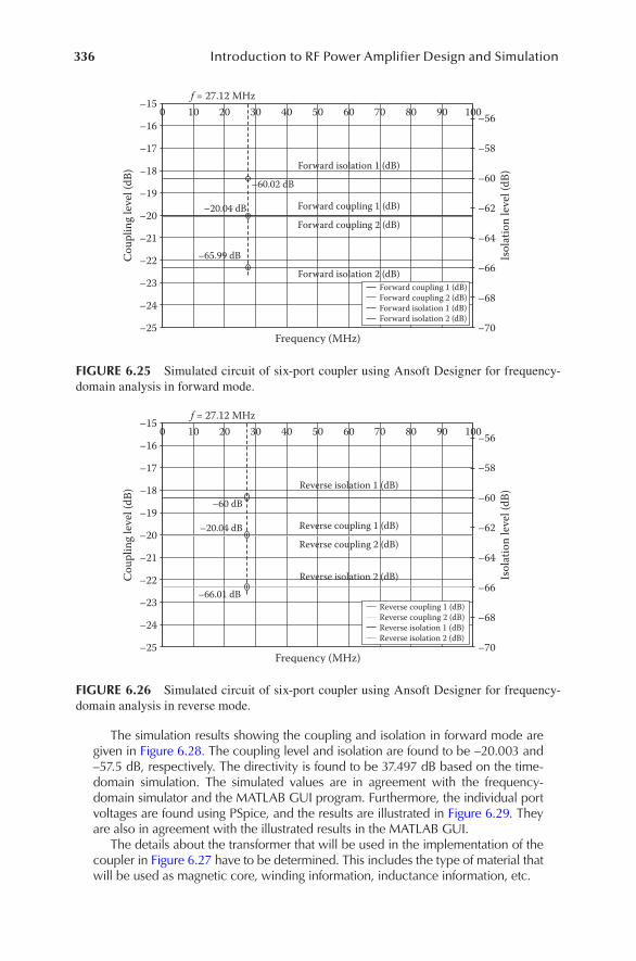
336 Introduction to RF Power Amplifier Design and Simulation
The simulation results showing the coupling and isolation in forward mode are given in Figure 6.28. The coupling level and isolation are found to be −20.003 and –57.5 dB, respectively. The directivity is found to be 37.497 dB based on the time-domain simulation. The simulated values are in agreement with the frequency-domain simulator and the MATLAB GUI program. Furthermore, the individual port voltages are found using PSpice, and the results are illustrated in Figure 6.29. They are also in agreement with the illustrated results in the MATLAB GUI.
The details about the transformer that will be used in the implementation of the coupler in Figure 6.27 have to be determined. This includes the type of material that will be used as magnetic core, winding information, inductance information, etc.
–150 10 20 30 40 50
Forward isolation 1 (dB)
Forward isolation 2 (dB)
Frequency (MHz)
Coup
ling
leve
l (dB
)
Isol
atio
n le
vel (
dB)
Forward coupling 1 (dB)
Forward coupling 2 (dB)
60 70 80 90 100–16
–56
–58
–60–60.02 dB
–20.04 dB
f = 27.12 MHz
–65.99 dB
–62
–64
–66
–68
–70
–17
–18
–19
–20
–21
–22
–23
–24
–25
Forward coupling 1 (dB)Forward coupling 2 (dB)Forward isolation 1 (dB)Forward isolation 2 (dB)
FIGURE 6.25 Simulated circuit of six-port coupler using Ansoft Designer for frequency-domain analysis in forward mode.
–150 10 20 30 40 50
Reverse isolation 1 (dB)
Reverse isolation 2 (dB)
Frequency (MHz)
Coup
ling
leve
l (dB
)
Isol
atio
n le
vel (
dB)
Reverse coupling 1 (dB)
Reverse coupling 2 (dB)
60 70 80 90 100–16
–56
–58
–60–60 dB
–20.04 dB
f = 27.12 MHz
–66.01 dB
–62
–64
–66
–68
–70
–17
–18
–19
–20
–21
–22
–23
–24
–25
Reverse coupling 1 (dB)Reverse coupling 2 (dB)Reverse isolation 1 (dB)Reverse isolation 2 (dB)
FIGURE 6.26 Simulated circuit of six-port coupler using Ansoft Designer for frequency-domain analysis in reverse mode.
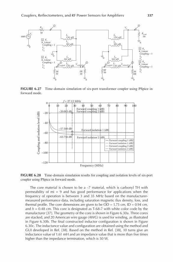
337Couplers, Reflectometers, and RF Power Sensors for Amplifiers
The core material is chosen to be a –7 material, which is carbonyl TH with permeability of mi = 9 and has good performance for applications when the frequency of operation is between 3 and 35 MHz based on the manufacturer-measured performance data, including saturation magnetic flux density, loss, and thermal profile. The core dimensions are given to be OD = 1.75 cm, ID = 0.94 cm, and h = 0.48 cm. This core is designated as T-68-7 with white color code by the manufacturer [37]. The geometry of the core is shown in Figure 6.30a. Three cores are stacked, and 20 American wire gauge (AWG) is used for winding, as illustrated in Figure 6.30b. The final constructed inductor configuration is shown in Figure 6.30c. The inductance value and configuration are obtained using the method and GUI developed in Ref. [38]. Based on the method in Ref. [38], 10 turns give an inductance value of 1.61 mH and an impedance value that is more than five times higher than the impedance termination, which is 50 W.
V
V V V V
V
K
K
K
K
+–100V
0
00
0
0
000
V150
K1K_LinearCoupling = 1L1L2
L11.61 µHL2161 µH
L41.61 µHVcoupled1 Visolated1 Vcoupled2 Visolated2L71.61 µH
50FF
FR50
RF50
RLoad50
Vo
50RR
L3161 µHL8161 µH
L61.61 µH
L5161 µH
K5K_LinearCoupling = 1L6L5
K6K_LinearCoupling = 1L8L7
K2K_LinearCoupling = 1L3L4
R12
FIGURE 6.27 Time-domain simulation of six-port transformer coupler using PSpice in forward mode.
00
–20
–40
–60
–80
–100
–120Frequency (MHz)
Coup
ling
and
isola
tion
leve
l (dB
)
10 20 30f = 27.12 MHz
–20.003 dBForward coupling 1 (dB)Forward coupling 2 (dB)
Forward isolation 1 (dB)
Forward isolation 2 (dB)
–57.500 dB
–63.756 dB
40 50 60 70 80 90 100
Forward coupling 1 (dB)Forward isolation 1 (dB)Forward coupling 2 (dB)Forward isolation 2 (dB)
FIGURE 6.28 Time-domain simulation results for coupling and isolation levels of six-port coupler using PSpice in forward mode.
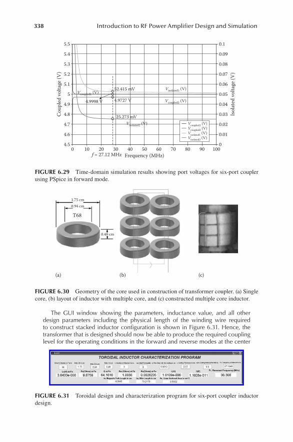
338 Introduction to RF Power Amplifier Design and Simulation
The GUI window showing the parameters, inductance value, and all other design parameters including the physical length of the winding wire required to construct stacked inductor configuration is shown in Figure 6.31. Hence, the transformer that is designed should now be able to produce the required coupling level for the operating conditions in the forward and reverse modes at the center
0
5.5
5.4
5.3
5.2
5.1
5
4.9
4.8
4.7
4.6
4.5
0.1
0.09
0.08
0.07
0.06
0.05
0.04
0.03
0.02
0.01
0
Frequency (MHz)
Coup
led
volta
ge (V
)
Isol
ated
volta
ge (V
)
10 20 30f = 27.12 MHz
Vcoupled1 (V)Visolated1 (V)
Visolated2 (V)
Vcoupled2 (V)
25.273 mV
4.9727 V4.9998 V
52.415 mV
40 50 60 70 80 90 100
Vcoupled1 (V)Vcoupled2 (V)Visolated1 (V)Visolated2 (V)
FIGURE 6.29 Time-domain simulation results showing port voltages for six-port coupler using PSpice in forward mode.
(a)
T68
1.75 cm0.94 cm
0.48 cm
(b) (c)
FIGURE 6.30 Geometry of the core used in construction of transformer coupler. (a) Single core, (b) layout of inductor with multiple core, and (c) constructed multiple core inductor.
FIGURE 6.31 Toroidal design and characterization program for six-port coupler inductor design.
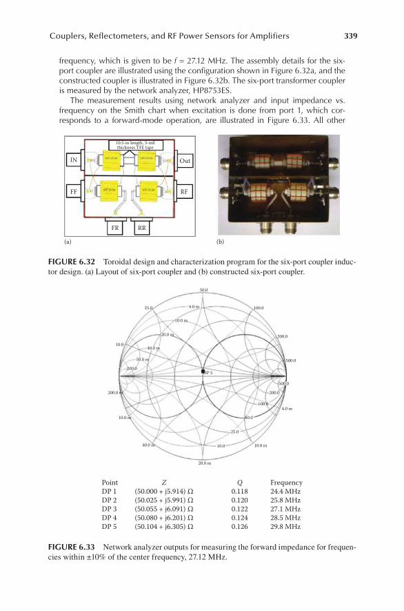
339Couplers, Reflectometers, and RF Power Sensors for Amplifiers
frequency, which is given to be f = 27.12 MHz. The assembly details for the six-port coupler are illustrated using the configuration shown in Figure 6.32a, and the constructed coupler is illustrated in Figure 6.32b. The six-port transformer coupler is measured by the network analyzer, HP8753ES.
The measurement results using network analyzer and input impedance vs. frequency on the Smith chart when excitation is done from port 1, which cor-responds to a forward-mode operation, are illustrated in Figure 6.33. All other
IN
FF
Out
10.5-in length, 3-milthickness TFE tape
RF
RRFR
(a) (b)
10T/1F/20 10T/1F/20
10T/1F/2010T/1F/20
FIGURE 6.32 Toroidal design and characterization program for the six-port coupler induc-tor design. (a) Layout of six-port coupler and (b) constructed six-port coupler.
PointDP 1DP 2DP 3DP 4DP 5
Z(50.000 + j5.914) Ω(50.025 + j5.991) Ω(50.055 + j6.091) Ω(50.080 + j6.201) Ω(50.104 + j6.305) Ω
Q0.1180.1200.1220.1240.126
Frequency24.4 MHz25.8 MHz27.1 MHz28.5 MHz29.8 MHz
50.0
100.0
200.0
500.0
4.0 m
10.0 m
20.0 m
40.0 m
10.0 m
200.0 m
10.0
25.0
200.0
4.0 m
10.0 m
20.0 m
40.0 m
50.0 m
10.0
25.0
50.0
100.0
200.0
500.0
DP 5
FIGURE 6.33 Network analyzer outputs for measuring the forward impedance for frequen-cies within ±10% of the center frequency, 27.12 MHz.
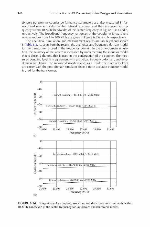
340 Introduction to RF Power Amplifier Design and Simulation
six-port transformer coupler performance parameters are also measured in for-ward and reverse modes by the network analyzer, and they are given vs. fre-quency within 10-MHz bandwidth of the center frequency in Figure 6.34a and b, respectively. The broadband frequency responses of the coupler in forward and reverse modes from 1 to 100 MHz are given in Figure 6.35a and b, respectively.
The analytical, simulation, and measurement results are tabulated and shown in Table 6.2. As seen from the results, the analytical and frequency-domain model for the transformer is used in the frequency domain. In the time-domain simula-tion, the accuracy of the system is increased by implementing the inductor model that is close to the one that is used in the construction of the coupler. The mea-sured coupling level is in agreement with analytical, frequency-domain, and time-domain simulators. The measured isolation and, as a result, the directivity level are closer with the time-domain simulator since a more accurate inductor model is used for the transformer.
0
–10
–20
–30
–40
–50
–6021.696 23.696 25.696
Forward coupling = –20.14 dB @ f = 27.12 MHz
Forward directivity = –34.664 dB @ f = 27.12 MHz
Forward isolation = –54.793 dB @ f = 27.12 MHz
27.696Frequency (MHz)
(a)
Forw
ard
mod
e (dB
)
29.696 31.696
0
–10
–20
–30
–40
–50
–6021.696 23.696 25.696
Reverse coupling = –20.15 dB @ f = 27.12 MHz
Reverse directivity = –34.672 dB @ f = 27.12 MHz
Reverse isolation = –54.822 dB @ f = 27.12 MHz
27.696Frequency (MHz)
(b)
Reve
rse m
ode (
dB)
29.696 31.696
FIGURE 6.34 Six-port coupler coupling, isolation, and directivity measurements within 10-MHz bandwidth of the center frequency for (a) forward and (b) reverse modes.
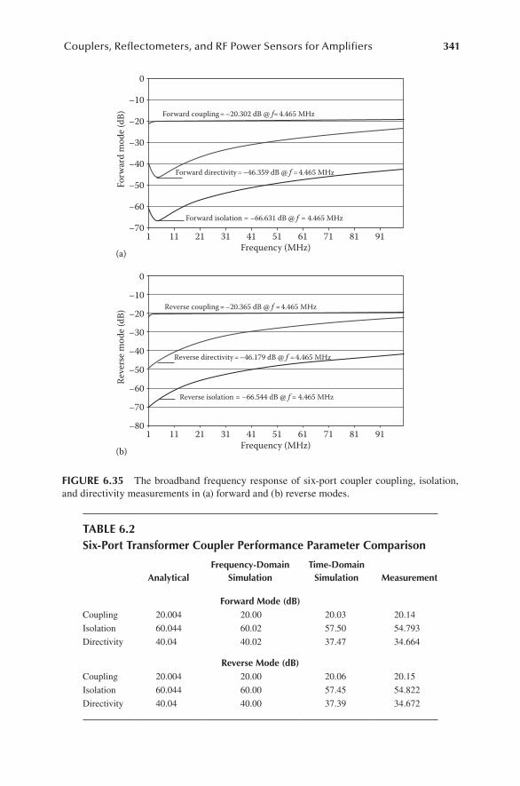
341Couplers, Reflectometers, and RF Power Sensors for Amplifiers
0
–10
–20
–30
–40
–50
–70
–60
1 11 21 31 41
Forward coupling = –20.302 dB @ f= 4.465 MHz
Forward directivity = –46.359 dB @ f = 4.465 MHz
Forward isolation = –66.631 dB @ f = 4.465 MHz
51 61Frequency (MHz)(a)
Forw
ard
mod
e (dB
)
71 9181
0
–10
–20
–30
–40
–50
–80
–70
–60
1 11 21 31 41
Reverse coupling = –20.365 dB @ f = 4.465 MHz
Reverse directivity = –46.179 dB @ f = 4.465 MHz
Reverse isolation = –66.544 dB @ f = 4.465 MHz
51 61Frequency (MHz)(b)
Reve
rse m
ode (
dB)
71 9181
FIGURE 6.35 The broadband frequency response of six-port coupler coupling, isolation, and directivity measurements in (a) forward and (b) reverse modes.
TABLE 6.2Six-Port Transformer Coupler Performance Parameter Comparison
AnalyticalFrequency-Domain
SimulationTime-Domain
Simulation Measurement
Forward Mode (dB)Coupling 20.004 20.00 20.03 20.14
Isolation 60.044 60.02 57.50 54.793
Directivity 40.04 40.02 37.47 34.664
Reverse Mode (dB)Coupling 20.004 20.00 20.06 20.15
Isolation 60.044 60.00 57.45 54.822
Directivity 40.04 40.00 37.39 34.672
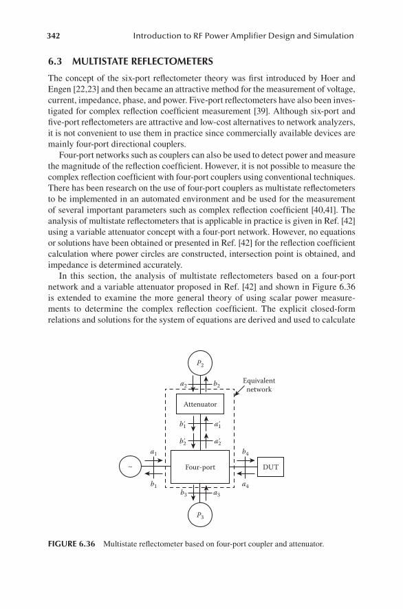
342 Introduction to RF Power Amplifier Design and Simulation
6.3 MULTISTATE REFLECTOMETERS
The concept of the six-port reflectometer theory was first introduced by Hoer and Engen [22,23] and then became an attractive method for the measurement of voltage, current, impedance, phase, and power. Five-port reflectometers have also been inves-tigated for complex reflection coefficient measurement [39]. Although six-port and five-port reflectometers are attractive and low-cost alternatives to network analyzers, it is not convenient to use them in practice since commercially available devices are mainly four-port directional couplers.
Four-port networks such as couplers can also be used to detect power and measure the magnitude of the reflection coefficient. However, it is not possible to measure the complex reflection coefficient with four-port couplers using conventional techniques. There has been research on the use of four-port couplers as multistate reflectometers to be implemented in an automated environment and be used for the measurement of several important parameters such as complex reflection coefficient [40,41]. The analysis of multistate reflectometers that is applicable in practice is given in Ref. [42] using a variable attenuator concept with a four-port network. However, no equations or solutions have been obtained or presented in Ref. [42] for the reflection coefficient calculation where power circles are constructed, intersection point is obtained, and impedance is determined accurately.
In this section, the analysis of multistate reflectometers based on a four-port network and a variable attenuator proposed in Ref. [42] and shown in Figure 6.36 is extended to examine the more general theory of using scalar power measure-ments to determine the complex reflection coefficient. The explicit closed-form relations and solutions for the system of equations are derived and used to calculate
P2
b2Equivalent
networka2
a1b1
a2b2
a3
a4
b4
b1
a1
b3
Four-port
Attenuator
DUT~
P3
FIGURE 6.36 Multistate reflectometer based on four-port coupler and attenuator.
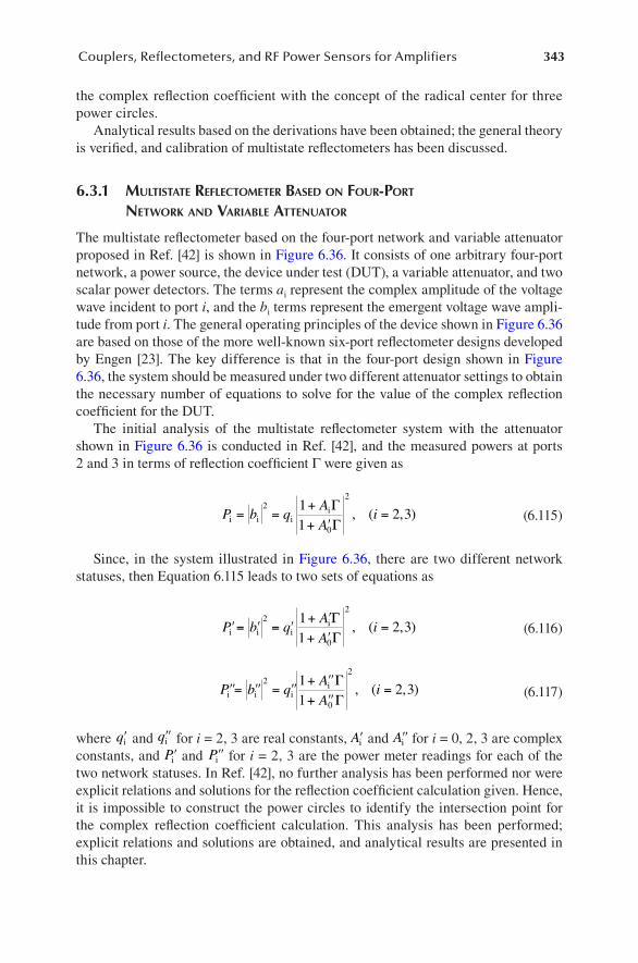
343Couplers, Reflectometers, and RF Power Sensors for Amplifiers
the complex reflection coefficient with the concept of the radical center for three power circles.
Analytical results based on the derivations have been obtained; the general theory is verified, and calibration of multistate reflectometers has been discussed.
6.3.1 Multistate reflectoMeter BaseD on four-port network anD VariaBle attenuator
The multistate reflectometer based on the four-port network and variable attenuator proposed in Ref. [42] is shown in Figure 6.36. It consists of one arbitrary four-port network, a power source, the device under test (DUT), a variable attenuator, and two scalar power detectors. The terms ai represent the complex amplitude of the voltage wave incident to port i, and the bi terms represent the emergent voltage wave ampli-tude from port i. The general operating principles of the device shown in Figure 6.36 are based on those of the more well-known six-port reflectometer designs developed by Engen [23]. The key difference is that in the four-port design shown in Figure 6.36, the system should be measured under two different attenuator settings to obtain the necessary number of equations to solve for the value of the complex reflection coefficient for the DUT.
The initial analysis of the multistate reflectometer system with the attenuator shown in Figure 6.36 is conducted in Ref. [42], and the measured powers at ports 2 and 3 in terms of reflection coefficient Γ were given as
P b qAA
ii i ii= =
++ ′
=2
0
211
2 3ΓΓ
, ( , ) (6.115)
Since, in the system illustrated in Figure 6.36, there are two different network statuses, then Equation 6.115 leads to two sets of equations as
′= ′ = ′+ ′+ ′
=P b qAA
ii i ii2
0
211
2 3ΓΓ
, ( , ) (6.116)
′′= ′′ = ′′+ ′′+ ′′
=P b qAA
ii i ii2
0
211
2 3ΓΓ
, ( , ) (6.117)
where ′qi and ′′qi for i = 2, 3 are real constants, ′Ai and ′′Ai for i = 0, 2, 3 are complex constants, and ′Pi and ′′Pi for i = 2, 3 are the power meter readings for each of the two network statuses. In Ref. [42], no further analysis has been performed nor were explicit relations and solutions for the reflection coefficient calculation given. Hence, it is impossible to construct the power circles to identify the intersection point for the complex reflection coefficient calculation. This analysis has been performed; explicit relations and solutions are obtained, and analytical results are presented in this chapter.
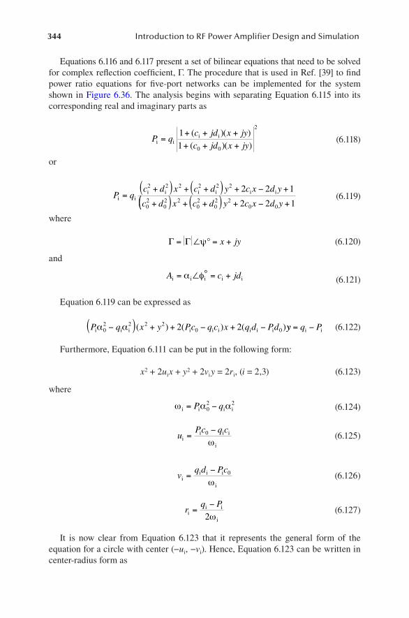
344 Introduction to RF Power Amplifier Design and Simulation
Equations 6.116 and 6.117 present a set of bilinear equations that need to be solved for complex reflection coefficient, Γ. The procedure that is used in Ref. [39] to find power ratio equations for five-port networks can be implemented for the system shown in Figure 6.36. The analysis begins with separating Equation 6.115 into its corresponding real and imaginary parts as
P qc jd x jyc jd x jyi ii i=
+ + ++ + +11 0 0
2( )( )( )( )
(6.118)
or
P qc d x c d y c x d y
c di i
i i i i i i=+( ) + +( ) + − +
+
2 2 2 2 2 2
02
02
2 2 1
(( ) + +( ) + − +x c d y c x d y202
02 2
0 02 2 1 (6.119)
where
Γ Γ= ∠ = +ψ° x jy (6.120)
and
A c jdi i i i i= ∠ ° = +α φ (6.121)
Equation 6.119 can be expressed as
P q x y Pc q c x q d Pdi i i i i i i i iα α02 2 2 2
0 02 2−( ) + + − + −( ) ( ) ( )yy q P= −i i (6.122)
Furthermore, Equation 6.111 can be put in the following form:
x2 + 2uix + y2 + 2vi y = 2ri, (i = 2,3) (6.123)
where
ω α αi i i i= −P q02 2 (6.124)
uPc q c
ii i i
i
=−0
ω (6.125)
vq d Pc
ii i i
i
=− 0
ω (6.126)
rq P
ii i
i
=−2ω
(6.127)
It is now clear from Equation 6.123 that it represents the general form of the equation for a circle with center (−ui, −vi). Hence, Equation 6.123 can be written in center-radius form as
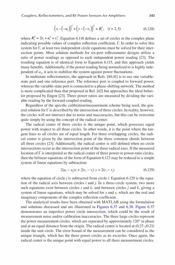
345Couplers, Reflectometers, and RF Power Sensors for Amplifiers
x u y v R i− −( )( ) + − −( )( ) = =i i i
2 22 2 3, ( , ) (6.128)
where R r u vi i i i2 2 22= + + . Equation 6.118 defines a set of circles in the complex plane
indicating possible values of complex reflection coefficient, Γ. In order to solve this system for Γ, at least two independent circle equations must be solved for their inter-section points. Most solution methods for six-port reflectometer designs utilize a ratio of power readings as opposed to each independent power reading [23]. The resulting equation is of identical form to Equation 6.115, and this approach yields many benefits. Additionally, if the power reading being normalized to is highly inde-pendent of a2, it acts to stabilize the system against power fluctuations.
In multistate reflectometers, the approach in Refs. [40,41] is to use one variable-state port and one reference port. The reference port is coupled to forward power, whereas the variable-state port is connected to a phase-shifting network. The method is more complicated than that proposed in Ref. [42] but approaches the ideal behav-ior proposed by Engen [23]. Three power ratios are measured by dividing the vari-able reading by the forward-coupled reading.
Regardless of the specific calibration/measurement scheme being used, the gen-eral solution for Γ is described by the intersection of three circles. In reality, however, the circles will not intersect due to noise and inaccuracies, but this can be overcome quite simply by using the concept of the radical center.
The radical center of three circles is the unique point, which possesses equal power with respect to all three circles. In other words, it is the point where the tan-gent lines to all circles are of equal length. For three overlapping circles, the radi-cal center is given by the intersection point of the three common chords between all three circles [23]. Additionally, the radical center is still defined when no circle intersections occur as the intersection point of the three radical axes. If the measured location of Γ is interpreted as the radical center of three power or power-ratio circles, then the bilinear equations of the form of Equation 6.123 may be reduced to a simple system of linear equations by subtraction:
2(ui − uj)x + 2(vi − vj) y = 2(ri − rj) (6.129)
where the equation of circle j is subtracted from circle i. Equation 6.129 is the equa-tion of the radical axis between circles i and j. In a three-circle system, two more such equations exist between circles i and k, and between circles j and k, giving a system of linear equations, which may be solved for x and y, which are the real and imaginary components of the complex reflection coefficient.
The analytical results have been obtained with MATLAB using the formulation and solutions discussed and are illustrated in Figures 6.37 and 6.38. Figure 6.37 demonstrates an imperfect power circle intersection, which could be the result of measurement noise and/or calibration inaccuracies. The three large circles represent the power measurement circles, which are separated by approximately 120° in phase and at an equal distance from the origin. The radical center is located at (0.27–j0.21) inside the unit circle. The error bound of the measurement can be considered as the unique triangle, which has the three power circles as its excircles. Once again, the radical center is the unique point with equal power to all three measurement circles.
346 Introduction to RF Power Amplifier Design and Simulation
Figure 6.38 illustrates the case of a near intersection of the three power circles for complex reflection coefficient determination. The radical axes are clearly shown as the lines passing through the common chords of each circle intersection. The error
Imag
inar
y
–2–2
–1.5
–0.5
0
0.5
1
1.5
2
–1
–1.5 –1 –0.5 0Real
Imperfect intersection
0.5 1 1.5 2
FIGURE 6.37 Illustration of imperfect power circle for complex reflection coefficient determination.
Imag
inar
y
–2–2
–1.5
–0.5
0
0.5
1
1.5
2
–1
–1.5 –1 –0.5 0Real
Near intersection case
0.5 1 1.5 2
FIGURE 6.38 Illustration of near intersection power circle for complex reflection coef-ficient determination.
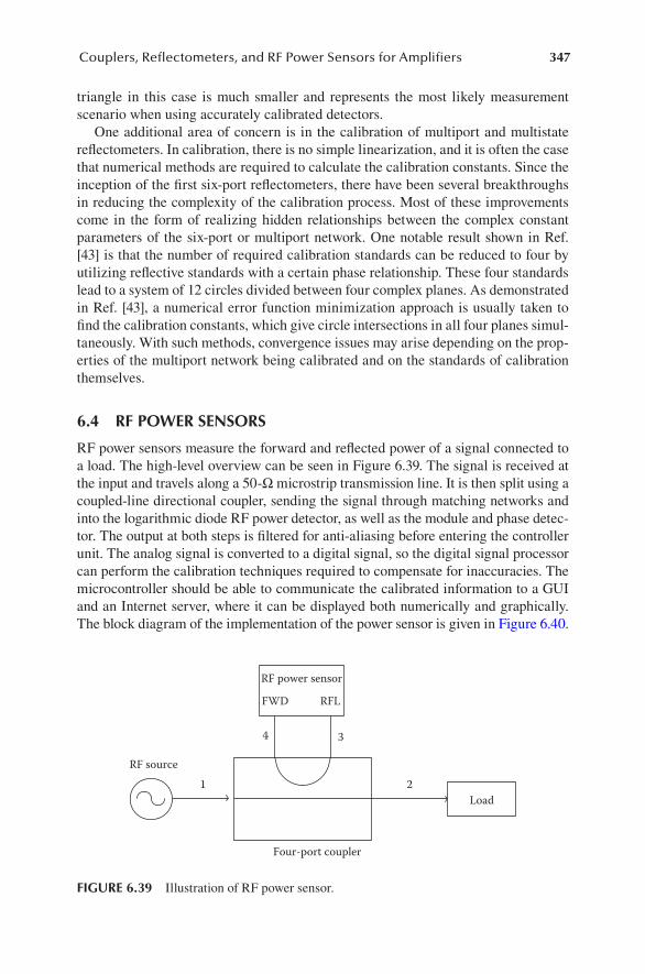
347Couplers, Reflectometers, and RF Power Sensors for Amplifiers
triangle in this case is much smaller and represents the most likely measurement scenario when using accurately calibrated detectors.
One additional area of concern is in the calibration of multiport and multistate reflectometers. In calibration, there is no simple linearization, and it is often the case that numerical methods are required to calculate the calibration constants. Since the inception of the first six-port reflectometers, there have been several breakthroughs in reducing the complexity of the calibration process. Most of these improvements come in the form of realizing hidden relationships between the complex constant parameters of the six-port or multiport network. One notable result shown in Ref. [43] is that the number of required calibration standards can be reduced to four by utilizing reflective standards with a certain phase relationship. These four standards lead to a system of 12 circles divided between four complex planes. As demonstrated in Ref. [43], a numerical error function minimization approach is usually taken to find the calibration constants, which give circle intersections in all four planes simul-taneously. With such methods, convergence issues may arise depending on the prop-erties of the multiport network being calibrated and on the standards of calibration themselves.
6.4 RF POWER SENSORS
RF power sensors measure the forward and reflected power of a signal connected to a load. The high-level overview can be seen in Figure 6.39. The signal is received at the input and travels along a 50-Ω microstrip transmission line. It is then split using a coupled-line directional coupler, sending the signal through matching networks and into the logarithmic diode RF power detector, as well as the module and phase detec-tor. The output at both steps is filtered for anti-aliasing before entering the controller unit. The analog signal is converted to a digital signal, so the digital signal processor can perform the calibration techniques required to compensate for inaccuracies. The microcontroller should be able to communicate the calibrated information to a GUI and an Internet server, where it can be displayed both numerically and graphically. The block diagram of the implementation of the power sensor is given in Figure 6.40.
1RF source
Load
FWD RFL
Four-port coupler
RF power sensor
2
4 3
FIGURE 6.39 Illustration of RF power sensor.
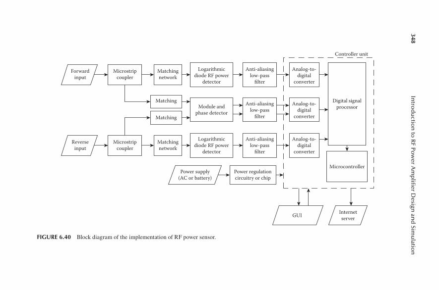
348In
trod
uctio
n to
RF Po
wer A
mp
lifier D
esign an
d Sim
ulatio
n
Controller unit
Digital signalprocessor
Analog-to-digital
converter
Analog-to-digital
converter
Analog-to-digital
converter
Anti-aliasinglow-pass
filter
Anti-aliasinglow-pass
filter
Module andphase detector
Anti-aliasinglow-pass
filter
Logarithmicdiode RF power
detector
Matchingnetwork
Matching
Matching
Matchingnetwork
Microstripcoupler
Microstripcoupler
Forwardinput
Reverseinput
Logarithmicdiode RF power
detector
Microcontroller
InternetserverGUI
Power regulationcircuitry or chip
Power supply(AC or battery)
FIGURE 6.40 Block diagram of the implementation of RF power sensor.
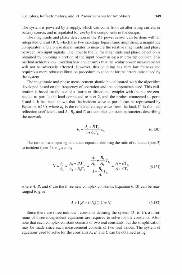
349Couplers, Reflectometers, and RF Power Sensors for Amplifiers
The system is powered by a supply, which can come from an alternating current or battery source, and is regulated for use by the components in the design.
The magnitude and phase detection in the RF power sensor can be done with an integrated circuit (IC), which has two six-stage logarithmic amplifiers, a magnitude comparator, and a phase discriminator to measure the relative magnitude and phase between two input signals. The input to the IC for magnitude and phase detection is obtained by coupling a portion of the input power using a microstrip coupler. This method achieves low insertion loss and ensures that the scalar power measurements will not be adversely affected. However, this coupling has very low flatness and requires a more robust calibration procedure to account for the errors introduced by the system.
The magnitude and phase measurement should be calibrated with the algorithm developed based on the frequency of operation and the components used. This cali-bration is based on the use of a four-port directional coupler with the source con-nected to port 1, the load connected to port 2, and the probes connected to ports 3 and 4. It has been shown that the incident wave at port 1 can be represented by Equation 6.130, where aL is the reflected voltage wave from the load, ΓL is the load reflection coefficient, and Ai, Bi, and C are complex constant parameters describing the network:
bA B
Cai
i i L
LL=
++
ΓΓ1
(6.130)
The ratio of two input signals, so an equation defining the ratio of reflected (port 3) to incident (port 4), is given by
Nbb
A BA B
AA
BABA
A B= =
++
=+
+=
+3
4
3 3
4 4
3
4
3
4
4
4
1
ΓΓ
Γ
Γ
ΓL
L
L
L
L
AA C+ ΓL
(6.131)
where A, B, and C are the three new complex constants. Equation 6.131 can be rear-ranged to give
A + ΓiB + (−NiΓi) C = Ni (6.132)
Since there are three unknown constants defining the system (A, B, C), a mini-mum of three independent equations are required to solve for the constants. Also, note that each complex constant consists of two real constants, but the simplification may be made since each measurement consists of two real values. The system of equations used to solve for the constants A, B, and C can be obtained using
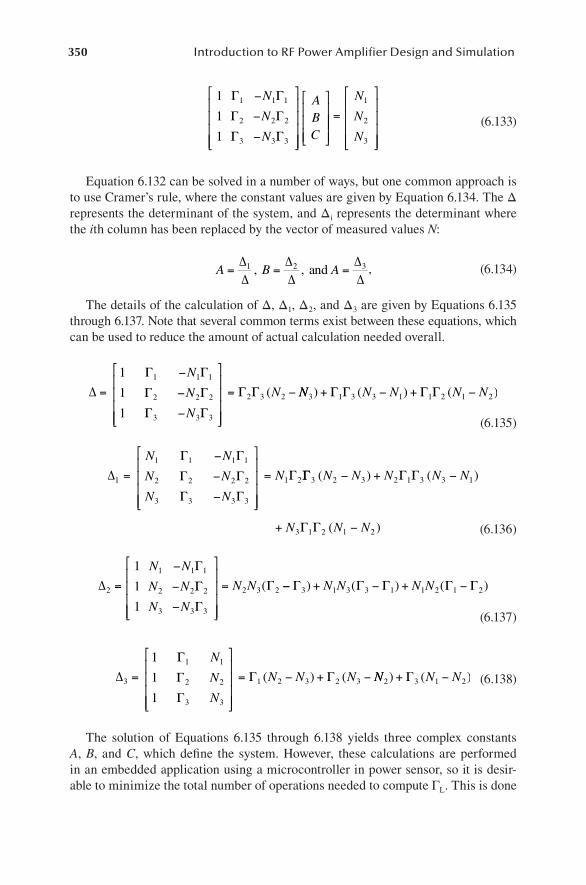
350 Introduction to RF Power Amplifier Design and Simulation
1
1
1
1 1 1
2 2 2
3 3 3
Γ Γ
Γ Γ
Γ Γ
−
−
−
N
N
N
ABC
=
N
N
N
1
2
3
(6.133)
Equation 6.132 can be solved in a number of ways, but one common approach is to use Cramer’s rule, where the constant values are given by Equation 6.134. The Δ represents the determinant of the system, and Δi represents the determinant where the ith column has been replaced by the vector of measured values N:
A B A= = =∆∆
∆∆
∆∆
1 2 3, , and , (6.134)
The details of the calculation of Δ, Δ1, Δ2, and Δ3 are given by Equations 6.135 through 6.137. Note that several common terms exist between these equations, which can be used to reduce the amount of actual calculation needed overall.
∆ =
−
−
−
= −
1
1
1
1 1 1
2 2 2
3 3 3
2 3 2
Γ Γ
Γ Γ
Γ Γ
Γ Γ
N
N
N
N( NN N N N N3 1 3 3 1 1 2 1 2) ( ) ( )+ − + −Γ Γ Γ Γ
(6.135)
∆1
1 1 1 1
2 2 2 2
3 3 3 3
1 2=
−
−
−
=
N N
N N
N N
N
Γ Γ
Γ Γ
Γ Γ
Γ ΓΓ Γ Γ
Γ Γ
3 2 3 2 1 3 3 1
3 1 2 1 2
( ) ( )
( )
N N N N N
N N N
− + −
+ − (6.136)
∆2
1 1 1
2 2 2
3 3 3
2 3 2
1
1
1
=
−
−
−
=
N N
N N
N N
N N
Γ
Γ
Γ
Γ( −− + − + −Γ Γ Γ Γ Γ3 1 3 3 1 1 2 1 2) ( ) ( )N N N N
(6.137)
∆3
1 1
2 2
3 3
1 2 3 2 3
1
1
1
=
= − + −
Γ
Γ
Γ
Γ Γ
N
N
N
N N N( ) ( NN N N2 3 1 2) ( )+ −Γ (6.138)
The solution of Equations 6.135 through 6.138 yields three complex constants A, B, and C, which define the system. However, these calculations are performed in an embedded application using a microcontroller in power sensor, so it is desir-able to minimize the total number of operations needed to compute ΓL. This is done
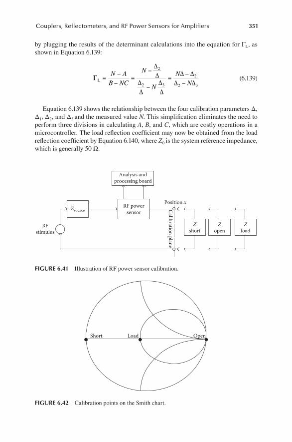
351Couplers, Reflectometers, and RF Power Sensors for Amplifiers
by plugging the results of the determinant calculations into the equation for ΓL, as shown in Equation 6.139:
ΓL =−−
=−
−=
−−
N AB NC
N
N
NN
∆∆
∆∆
∆∆
∆ ∆∆ ∆
2
2 3
2
2 3
(6.139)
Equation 6.139 shows the relationship between the four calibration parameters Δ, Δ1, Δ2, and Δ3 and the measured value N. This simplification eliminates the need to perform three divisions in calculating A, B, and C, which are costly operations in a microcontroller. The load reflection coefficient may now be obtained from the load reflection coefficient by Equation 6.140, where Z0 is the system reference impedance, which is generally 50 Ω.
RFstimulus
ZsourceRF power
sensor
Analysis andprocessing board
Position x
Calibration plane
Zshort
Zopen
Zload
FIGURE 6.41 Illustration of RF power sensor calibration.
OpenShort Load
FIGURE 6.42 Calibration points on the Smith chart.
352 Introduction to RF Power Amplifier Design and Simulation
Z ZL oL
L
=+−
11
ΓΓ
(6.140)
The typical sensor calibration that takes place before the measurement is shown in Figure 6.41. It consists of a sequence of connection and calibration based on the known load standards such as short, open, and 50-Ω load. Calibration points for these impedances are shown in Figure 6.42.
PROBLEMS
1. Design a 20-dB two-line directional coupler using ROGERS 4003 at 1 GHz using the formulation given. Compare your results using a planar electro-magnetic simulator.
2. Design a 10-dB three-line coupler using FR4 at 1 GHz with the formulation given. Compare your results using a planar electromagnetic simulator.
3. Calculate and compare the directivity of the two-line and three-line cou-plers in Problem 1 for 20-dB directivity.
4. Design the multilayer configuration of the coupler given in Problem 1, and calculate and compare the directivity of the coupler for two-line, three-line, and multilayer configurations.
REFERENCES
1. A. Eroglu. 2013. RF Circuit Design Techniques for MF-UHF Applications. CRC Press, Boca Raton, FL.
2. A. Eroglu, and J.K. Lee. 2008. The complete design of microstrip directional couplers using the synthesis technique. IEEE Transactions on Instrumentation and Measurement, Vol. 57, No. 12, pp. 2756–2761, December.
3. G.D. Monteath. 1955. Coupled transmission lines as symmetrical directional couplers. Proceedings of the IEE—Part B: Radio and Electronic Engineering, Vol. 102, Pt. B, pp. 383–392, May.
4. N.A. El-Deeb. 1983. The calibration and performance of a microstrip six-port reflec-tometer. IEEE Transactions on Microwave Theory and Techniques, Vol. MTT-31, No. 7, pp. 509–514.
5. R.J. Collier, and N.A. El-Deeb. 1980. Microstrip coupler suitable for use as a six-port reflectometer. IEE Proceedings, Microwaves, Optics and Antennas, Vol. 127, No. 2, Pt. H, pp. 87–91, April.
6. M. Pavlidis, and H.L. Hartnagel. 1976. The design and performance of three-line microstrip couplers. IEEE Transactions on Microwave Theory and Techniques, Vol. MTT-24, pp. 631–640.
7. R.J. Collier, and N.A. El-Deeb. 1979. On the use of a microstrip three-line system as a six-port reflectometer. IEEE Transactions on Microwave Theory and Techniques, Vol. MTT-27, pp. 847–853.
8. A. Eroglu, R. Goulding, P. Ryan, J. Caughman, and D. Rasmussen. 2010. Novel broadband multilayer microstrip directional couplers. 2010 IEEE AP-S, pp. 1–4, July 11–17.

353Couplers, Reflectometers, and RF Power Sensors for Amplifiers
9. H. Park, and Y. Lee. 2010. Asymmetric coupled line directional coupler loaded with shunt inductors for directivity enhancement. Electronic Letters, Vol. 46, No. 6, pp. 425–426, March 18.
10. S. Lee, and Y. Lee. 2009. An inductor-loaded microstrip directional coupler for directiv-ity enhancement. IEEE Microwave and Wireless Components Letters, Vol. 19, No. 6, pp. 362–364, June.
11. S. Lee, and Y. Lee. 2010. A design method for microstrip directional couplers loaded with shunt inductors for directivity enhancement. IEEE Transactions on Microwave Theory and Techniques, Vol. 58, No. 4, pp. 994–1002, April.
12. R. Phromloungsri, V. Chamnanphrai, and M. Chongcheawchamnan. 2006. Design high-directivity parallel-coupled lines using quadrupled inductive-compensated technique. Proceedings of Asia-Pacific Microwave Conference, pp. 1380–1383.
13. D. Kajfez. 1978. Raise coupler directivity with lumped compensation. Microwaves, Vol. 27, pp. 64–70, March.
14. S.-M. Wang, C.-H. Chen, and C.-Y. Chang. 2003. A study of meandered microstrip coupler with high directivity. Microwave Symposium Digest, 2003 IEEE MTT-S International, Vol. 1, pp. 63–66.
15. K. Sachse. 1988. Analysis of asymmetrical inhomogeneous coupled line directional coupler. Microwave Conference, pp. 985–990.
16. S.L. March. 1982. Phase velocity compensation in parallel-coupled microstrip. 1982 MTT-S Int’1 Microwave Symposium Digest, pp. 410–412, May.
17. A. Eroglu. 2007. Design of three-line multi-layer microstrip directional couplers at HF for high power applications. Microwave Journal, Vol. 50, pp. 150–154, April.
18. J. Huang, Q. Hao, J. She, and Z. Feng. 2005. A six-port coupler with high directivity for VSWR measurement. APMC 2005 Proceedings.
19. C.A. Hoer. 1972. The six-port coupler: A new approach to measuring voltage, current, power, impedance, and phase. IEEE Transactions on Instrumentation and Measurement, Vol. IM-21, No. 4, pp. 466–470.
20. A.L. Cullen, S.K. Judah, and F. Nikravesh. 1980. Impedance measurement using a six-port directional coupler. IEE Proceedings, Microwaves, Optics and Antennas, Vol. 127, No. 2, Pt. H, pp. 92–98.
21. T.S. Cooper, G. Baldwin, and R. Farrell. 2006. Six-port precision directional coupler. Electronics Letters, Vol. 42, No. 21, pp. 1232–1233.
22. G.F. Engen, and C.A. Hoer. 1972. Application of an arbitrary six-port junction to power measurement problems. IEEE Transactions on Instrumentation and Measurement, Vol. 21, No. 4, pp. 470–474.
23. G.F. Engen. 1977. The six-port reflectometer; an alternative network analyser. IEEE Transactions on Microwave Theory and Techniques, Vol. MTT-25, pp. 1075–1080.
24. J.J. Yao, and S.P. Yeo. 2008. Six-port reflectometer based on modified hybrid couplers. IEEE Transactions on Microwave Theory and Techniques, Vol. 56, No. 2, pp. 493–498.
25. J.J. Yao, S.P. Yeo, and M.E. Bialkowski. 2009. Modifying branch-line coupler design to enhance six-port reflectometer performance. IEEE, International Microwave Symposium, pp. 1669–1672.
26. E.J. Griffin. 1982. Six-port reflectometer circuit comprising three directional couplers. Electronics Letters, Vol. 18, No. 12, pp. 491–493.
27. U. Stumper. 1990. Simple millimeter-wave six-port reflectometers. IEEE Conference on Precision Electromagnetic Measurements, pp. 51–52.
28. C. Akyel, and F.M. Ghannouchi. 1994. A new design for high-power six-port reflectome-ters using hybrid stripline/waveguide technology. IEEE Transactions on Instrumentation and Measurement, Vol. 43, No. 2, pp. 316–321.
29. A.S.S. Mohra. 2001. Six-port reflectometer realization using two microstrip three-section couplers. 18th National Radio Science Conference, March, Egypt.

354 Introduction to RF Power Amplifier Design and Simulation
30. E.R.B. Hansson, and G.P. Riblet. 1983. An ideal six-port network consisting of a matched reciprocal lossless five-port and a perfect directional coupler. IEEE Transactions on Microwave Theory and Techniques, Vol. 31, pp. 284–288.
31. J.A. Dobrowolski. 1982. Improved six-port circuit for complex reflection coefficient measurements. Electronics Letters, Vol. 18, No. 17, pp. 748–750.
32. F. Alessandri. 2003. A new multiple-tuned six-port Riblet-type directional coupler in rectangular waveguide. IEEE Transactions on Microwave Theory and Techniques, Vol. MTT-51, No. 5, pp. 1441–1448.
33. F.M. Ghannouchi, R.G. Bosisio, and Y. Demers. 1989. Load-pull characterization method using six-port techniques. 6th IEEE Instrumentation and Measurement Technology Conference, IMTC-89, pp. 536–539.
34. D. Lê, P. Poiré, and F.M. Ghannouchi. 1998. Six-port-based active source-pull measure-ment technique. Measurement Science and Technology, Vol. 9, No. 8, pp. 1336–1342.
35. J. Carr. 1999. Directional couplers. RF Design, pp. 676–677, August. 36. D. Kajfez. 1999. Scattering matrix of a directional coupler with ideal transformers.
IEEE Microwaves, Antennas and Propagation, Vol. 146, No. 4, pp. 295–297, August. 37. Micrometals. Available at http://www.micrometals.com/rfparts/rftoroid4.html. 38. A. Eroglu. 2012. Complete modeling of toroidal inductors for high power RF applica-
tions. IEEE Transactions on Magnetics, Vol. 48, No. 11, pp. 4526–4529, November. 39. L. Shihe, and R.G. Bosisio. 1983. The measurement of complex reflection coefficient
by means of a five-port reflectometer. IEEE Transactions on Microwave Theory and Techniques, Vol. 31, No. 4, pp. 321–326, April.
40. L.C. Oldfield, J.P. Ide, and E.J. Griffin. 1985. A multistate reflectometer. IEEE Transactions on Instrumentation and Measurement, Vol. 34, No. 2, pp. 198–201, June.
41. S.P. Yeo, and S.T. Tay. 2000. Improved design for multistate reflectometer (with two power detectors) for measuring reflection coefficients of microwave devices. IEEE Transactions on Instrumentation and Measurement, Vol. 49, No. 1, pp. 61–65, February.
42. Q. Sui, K. Wang, and L. Li. 2010. The measurement of complex reflection coefficient by means of an arbitrary four-port network and a variable attenuator. 2010 International Symposium on Signals Systems and Electronics (ISSSE), Vol. 2, pp. 1–3, September 17–20.
43. L. Qiao, and S.P. Yeo. 1995. Improved implementation of four-standard procedure for calibrating six-port reflectometers. IEEE Transactions on Instrumentation and Measurement, Vol. 44, No. 3, pp. 632–636, June.
355
7 Filter Design for RF Power Amplifiers
7.1 INTRODUCTION
In radio frequency (RF) power amplifiers, the main purpose of filters is to eliminate spurious and harmonic contents from the frequency of interest. Depending on the frequency of operation and application, a filter can be implemented using lumped elements or distributed elements, or it can comprise a mix of lumped and distrib-uted elements. Filters that are implemented with distributed elements are based on lumped-element filter prototype models. The lumped-element low-pass filter (LPF) prototypes are the basis of all the filter prototypes. Most of the filters are imple-mented using four conventional filter types: low pass, high pass, bandpass, and bandstop filters (BSFs). LPFs provide maximum power transfer at frequencies below cut-off or corner frequency, fc. The frequency is stopped above fc for LPFs. High-pass filters (HPFs) behave opposite to LPFs and pass signals at frequencies above fc. Bandpass filters (BPFs) pass signals at frequencies between lower and upper cut-off frequencies and stop everything else out of this frequency band. BSFs function opposite to BPFs and stop signals between lower and upper cut-off frequencies and pass everything else. The commonly used basic filter types are shown with their ideal frequency characteristics in Figure 7.1. There are also other filter types that can be designed and implemented for specific applications. Filters for amplifiers are interfaced as off-line filters or in-line filters. When they are implemented as off-line filters, they present a matched impedance to the amplifier signal at the operational frequency and present very high impedance at all other frequencies.
If the filters are implemented in-line filters, then they need to present a match impedance at the operational frequency and block signals at any other frequency depending on the application.
The common method to analyze filters is to treat them as lossless, linear two-port networks. The conventional filter design procedure for LPFs, HPFs, BPFs, or BSFs begins from LPF prototype and then involves impedance and frequency scaling, and filters transformation to HPFs, BPFs or BSFs to obtain final component values at the frequency of operation [1]. The design is then simulated and compared with specifications. The final step in the design of filters involves implementation and measurement of the filter response.
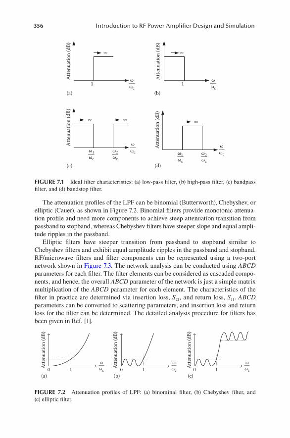
356 Introduction to RF Power Amplifier Design and Simulation
The attenuation profiles of the LPF can be binomial (Butterworth), Chebyshev, or elliptic (Cauer), as shown in Figure 7.2. Binomial filters provide monotonic attenua-tion profile and need more components to achieve steep attenuation transition from passband to stopband, whereas Chebyshev filters have steeper slope and equal ampli-tude ripples in the passband.
Elliptic filters have steeper transition from passband to stopband similar to Chebyshev filters and exhibit equal amplitude ripples in the passband and stopband. RF/microwave filters and filter components can be represented using a two-port network shown in Figure 7.3. The network analysis can be conducted using ABCD parameters for each filter. The filter elements can be considered as cascaded compo-nents, and hence, the overall ABCD parameter of the network is just a simple matrix multiplication of the ABCD parameter for each element. The characteristics of the filter in practice are determined via insertion loss, S21, and return loss, S11. ABCD parameters can be converted to scattering parameters, and insertion loss and return loss for the filter can be determined. The detailed analysis procedure for filters has been given in Ref. [1].
Atte
nuat
ion
(dB)
1
(a)
1
(b)
Atte
nuat
ion
(dB)
Atte
nuat
ion
(dB)
(c)A
ttenu
atio
n (d
B)(d)
∞∞
∞ ∞ ∞
ωωc
ωωcω1
ωc
ω2ωc
ωωc
ωωc
ω1ωc
ω2ωc
FIGURE 7.1 Ideal filter characteristics: (a) low-pass filter, (b) high-pass filter, (c) bandpass filter, and (d) bandstop filter.
Atte
nuat
ion
(dB)
(a)0 1
ωωc
Atte
nuat
ion
(dB)
(b)0 1
ωωc
Atte
nuat
ion
(dB)
(c)0 1
ωωc
FIGURE 7.2 Attenuation profiles of LPF: (a) binominal filter, (b) Chebyshev filter, and (c) elliptic filter.
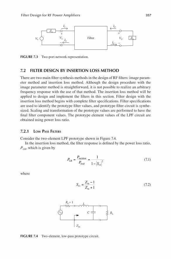
357Filter Design for RF Power Amplifiers
7.2 FILTER DESIGN BY INSERTION LOSS METHOD
There are two main filter synthesis methods in the design of RF filters: image param-eter method and insertion loss method. Although the design procedure with the image parameter method is straightforward, it is not possible to realize an arbitrary frequency response with the use of that method. The insertion loss method will be applied to design and implement the filters in this section. Filter design with the insertion loss method begins with complete filter specifications. Filter specifications are used to identify the prototype filter values, and prototype filter circuit is synthe-sized. Scaling and transformation of the prototype values are performed to have the final filter component values. The prototype element values of the LPF circuit are obtained using power loss ratio.
7.2.1 Low Pass FiLters
Consider the two-element LPF prototype shown in Figure 7.4.In the insertion loss method, the filter response is defined by the power loss ratio,
PLR, which is given by
PPP S
LRincident
load
= =−
1
1 11
2 (7.1)
where
SZZ11
11
=−+
in
in
(7.2)
Filter
I1
I2I1
I2
V1
+
–V2
+
–
Zs
Vs ZL
FIGURE 7.3 Two-port network representation.
Zin
Rs = 1
RL
L
C
FIGURE 7.4 Two-element, low-pass prototype circuit.
358 Introduction to RF Power Amplifier Design and Simulation
Pincident refers to the available power from the source, and Pload represents the power delivered to the load. As explained before, the attenuation characteristics of the fil-ter can fall into one of these three categories: binomial (Butterworth), Chebyshev, or elliptic. The binomial or Butterworth response provides the flattest passband response for a given filter and is defined by
P kN
LR = +
1 2
2ωωc
(7.3)
where k = 1, and N is the order of the filter. Chebyshev filters provide steeper transi-tion from passband to stopband while they have equal ripples in the passband, and their attenuation characteristics are defined by
P k TLR = +
1 2 2
Nc
ωω (7.4)
where TN is the Chebyshev polynomial. The prototype values of the filter circuit, L and C, shown in Figure 7.4 are found by solving Equations 7.1 through 7.4.
7.2.1.1 Binomial Filter ResponseBinomial filter response can be explained using Figure 7.4 for a two-element LPF network. Source impedance and cut-off frequency for the circuit in Figure 7.4 are assumed to be 1 Ω and 1 rad/s, respectively. In the LPF network, N = 2, and power loss becomes
PLR = 1 + ω4 (7.5)
The input impedance is found as
Zj L R C R j RC
R Cin =
+ + −
+
ω ω ω
ω
( ) ( )
( )
1 1
1
2 2 2
2 2 2 (7.6)
which leads to
S
j L R C R j RC
R C
j11
2 2 2
2 2 2
1 1
11
=
+ + −
+
−
ω ω ω
ω
ω
( ) ( )
( )
LL R C R j RC
R C
( ) ( )
( )
1 1
11
2 2 2
2 2 2
+ + −
+
+
ω ω
ω
(7.7)
The L and C values satisfying the equation are found to be
L = C = 1.4142 (7.8)
359Filter Design for RF Power Amplifiers
The same procedure is applied for LPF circuit with any number. The values obtained using this method are tabulated and given in Table 7.1 [1]. In essence, the two-element low-pass proto circuit analyzed is called a ladder network. Although the LPF circuit in Figure 7.4 begins with a series inductor, the analysis applies when it is switched with a shunt capacitor. In addition, the number of elements can be increased to N, and the ladder network can be generalized, as shown in Figure 7.5, where the values shown in Table 7.1 can be used for binomial response. In the low-pass prototype circuits in Figure 7.5, g0 represents the source resistance or conduc-tance, whereas gN+1 represents the load resistance or conductance. gN is an inductor for a series-connected component and a capacitor for a parallel-connected compo-nent. Attenuation curves for the low-pass prototype filters can be found from
Attenuation (dB) = 10 log(PLR) (7.9)
TABLE 7.1Component Values for Binomial LPF Response with g0 = 1, ωc = 1
N g1 g2 g3 g4 g5 g6 g7 g8 g9
1 2.0000 1.0000
2 1.4142 1.4142 1.0000
3 1.0000 2.0000 1.0000 1.0000
4 0.7654 1.8478 1.8478 0.7654 1.0000
5 0.6180 1.6180 2.0000 1.6180 0.6180 1.0000
6 0.5176 1.4142 1.9318 1.9318 1.4142 0.5176 1.0000
7 0.4450 1.2470 1.8019 2.0000 1.8019 1.2470 0.4450 1.0000
8 0.3902 1.1111 1.6629 1.9615 1.9615 1.6629 1.1111 0.3902 1.0000
Zin
Rs = g0 = 1 L2 = g2
gN+1C1 = g1 C3 = g3
Zin
Gs = g0 = 1 gN+1C2 = g2
L3 = g3L1 = g1
(a)
(b)
FIGURE 7.5 Low-pass prototype ladder networks: (a) first element shunt C; (b) first element series L.
360 Introduction to RF Power Amplifier Design and Simulation
Attenuation curves for binomial response using Equation 7.9 are obtained by MATLAB® and are given in Figure 7.6 [1]. Once the design filter specifications are given, the number of required elements to have the required attenuation is deter-mined from attenuation curves. In the second step, the table is used to determine the normalized component values for the required number of elements found in the previous stage. Then, scaling and transformation step are performed, and the final filter component values are obtained.
Since the original normalized component values of the LPF are designated as L, C, and RL, the final scaled component values of the filter with source impedance R0 are found from
′ =R Rs 0 (7.10)
′ =R R RL L0 (7.11)
′ =L RL
0n
cω (7.12)
′ =CCR
n
c0ω (7.13)
70
60
50
40
30
20
10
010–1 100ω/ωc – 1
101
n = 1
n = 2
n = 3
n = 4
n = 5
n = 6
n = 7
n = 8
n = 9n = 10
Attenuation curves versus ω/ωc – 1
Atte
nuat
ion
(dB)
FIGURE 7.6 Attenuation curves for binomial filter response for low-pass prototype circuits.
361Filter Design for RF Power Amplifiers
7.2.1.2 Chebyshev Filter ResponseThe Chebyshev filter response can be obtained similarly using the two-element, low-pass prototype circuit given in Figure 7.4. The power loss takes the following form when N = 2:
P k TLRc
= +
1 2
22 ω
ω (7.14)
where
T2
2
2 1ωω
ωωc c
=
− (7.15)
Substituting Equation 7.15 into Equation 7.14 gives
PLR = 1 + k2(4ω4 − 4ω2 + 1) (7.16)
The input impedance and S11 are given by Equations 7.6 and 7.7. When Equation 7.7 is substituted into Equation 7.1 with Equation 7.16, the L and C values satisfying the equation are found. Chebyshev polynomials up to the seventh order are given in Table 7.2 [1]. The polynomials given in Table 7.2 can be used to obtain design tables giving component values for various ripple values, as shown in Figure 7.7. Chebyshev polynomials are defined by a three-term recursion where
T0(x) = 1, T1(x) = x, Tn+1(x) = 2xTn(x) − Tn−1(x), n = 1, 2… (7.17)
where x = ω/ωc. The attenuation curves for Chebyshev LPF response are obtained from
Attenuation(dB) Nc
= +
′
10 1 2 2log ε
ωω
T (7.18)
where
ωω
ωωc c
′=
cosh( )B (7.19)
BN
=
−1 11cosh
ε (7.20)
ε = −10 110ripple dB( )
(7.21)

362 Introduction to RF Power Amplifier Design and Simulation
The attenuation curves are obtained and given for several ripple values using MATLAB in Ref. [1] with examples.
Example—F/2 LPF Design for RF Power Amplifiers
Design an F/2 filter for an RF power amplifier that is operating at 13.56 MHz. The filter should have no impact during the normal operation of the amplifier. It should have at least 20-dB attenuation at F/2 frequency. The passband ripple should not exceed 0.1-dB ripple. It is given that the amplifier is presenting 30-Ω impedance to load line.
Solution
In RF power amplifier applications, signals having frequency of F/2 may become an important problem that affects the signal purity and the amount of power deliv-ered to the load. This problem can be resolved by eliminating signals using LPFs commonly called the F/2 filter. The F/2 filter is connected off-line to the load line
TABLE 7.2Chebyshev Polynomials up to Seventh Order
Order of Polynomial, N TNωωωωc
1ωωc
2 2 12
ωωc
−
3 4 33
ωω
ωωc c
−
4 8 8 14 2
ωω
ωωc c
−
+
5 16 20 55 3
ωω
ωω
ωωc c c
−
+
6 32 48 18 16 4 2
ωω
ωω
ωωc c c
−
+
−
7 64 112 58 77 5 3
ωω
ωω
ωω
ωωc c c c
−
+
−
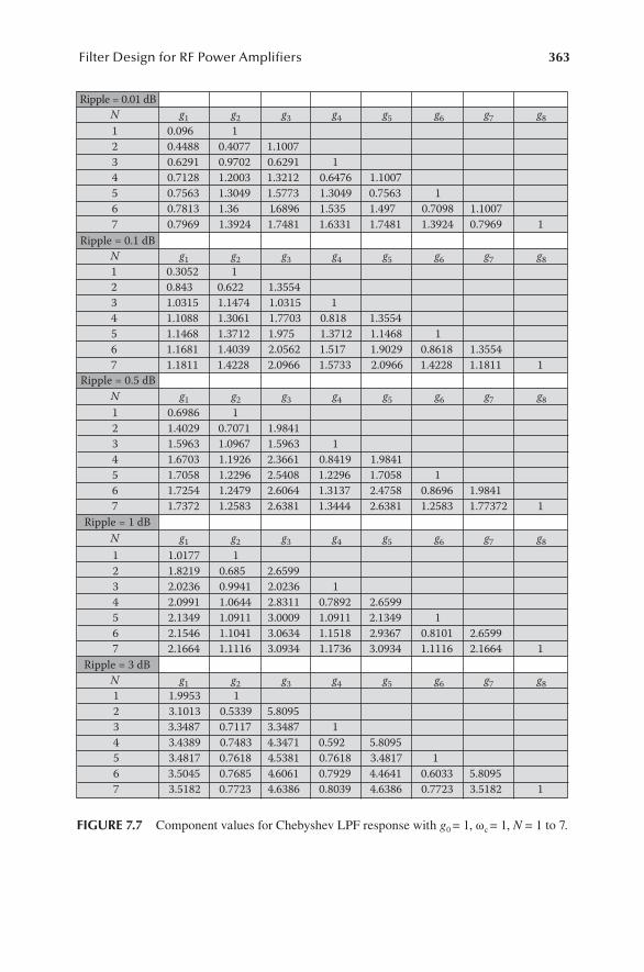
363Filter Design for RF Power Amplifiers
Ripple = 0.01 dBN g1 g2 g3 g4 g5 g6 g7 g8 1 0.096 12 0.4488 0.4077 1.10073 0.6291 0.9702 0.6291 14 0.7128 1.2003 1.3212 0.6476 1.10075 0.7563 1.3049 1.5773 1.3049 0.7563 16 0.7813 1.36 1.6896 1.535 1.497 0.7098 1.10077 0.7969 1.3924 1.7481 1.6331 1.7481 1.3924 0.7969 1
Ripple = 1 dB
1 1.0177 12 1.8219 0.685 2.65993 2.0236 0.9941 2.0236 14 2.0991 1.0644 2.8311 0.7892 2.65995 2.1349 1.0911 3.0009 1.0911 2.1349 16 2.1546 1.1041 3.0634 1.1518 2.9367 0.8101 2.65997 2.1664 1.1116 3.0934 1.1736 3.0934 1.1116 2.1664 1
Ripple = 0.1 dB
1 0.3052 12 0.843 0.622 1.35543 1.0315 1.1474 1.0315 14 1.1088 1.3061 1.7703 0.818 1.35545 1.1468 1.3712 1.975 1.3712 1.1468 16 1.1681 1.4039 2.0562 1.517 1.9029 0.8618 1.35547 1.1811 1.4228 2.0966 1.5733 2.0966 1.4228 1.1811 1
Ripple = 0.5 dB
1 0.6986 12 1.4029 0.7071 1.98413 1.5963 1.0967 1.5963 14 1.6703 1.1926 2.3661 0.8419 1.98415 1.7058 1.2296 2.5408 1.2296 1.7058 16 1.7254 1.2479 2.6064 1.3137 2.4758 0.8696 1.98417 1.7372 1.2583 2.6381 1.3444 2.6381 1.2583 1.77372 1
Ripple = 3 dB
1 1.9953 12 3.1013 0.5339 5.80953 3.3487 0.7117 3.3487 14 3.4389 0.7483 4.3471 0.592 5.80955 3.4817 0.7618 4.5381 0.7618 3.4817 16 3.5045 0.7685 4.6061 0.7929 4.4641 0.6033 5.80957 3.5182 0.7723 4.6386 0.8039 4.6386 0.7723 3.5182 1
N g1 g2 g3 g4 g5 g6 g7 g8
N g1 g2 g3 g4 g5 g6 g7 g8
N g1 g2 g3 g4 g5 g6 g7 g8
N g1 g2 g3 g4 g5 g6 g7 g8
FIGURE 7.7 Component values for Chebyshev LPF response with g0 = 1, ωc = 1, N = 1 to 7.
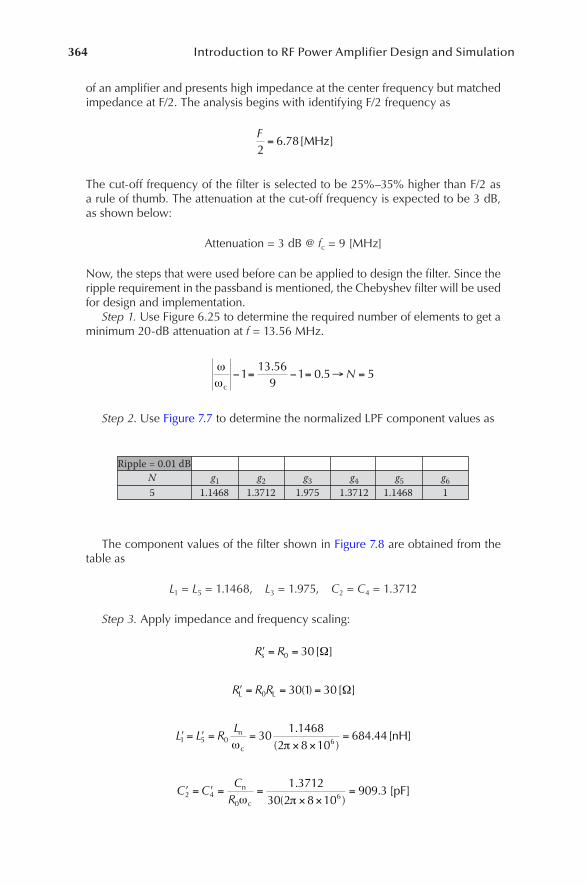
364 Introduction to RF Power Amplifier Design and Simulation
of an amplifier and presents high impedance at the center frequency but matched impedance at F/2. The analysis begins with identifying F/2 frequency as
F2
6 78= . [ ]MHz
The cut-off frequency of the filter is selected to be 25%–35% higher than F/2 as a rule of thumb. The attenuation at the cut-off frequency is expected to be 3 dB, as shown below:
Attenuation = 3 dB @ fc = 9 [MHz]
Now, the steps that were used before can be applied to design the filter. Since the ripple requirement in the passband is mentioned, the Chebyshev filter will be used for design and implementation.
Step 1. Use Figure 6.25 to determine the required number of elements to get a minimum 20-dB attenuation at f = 13.56 MHz.
ωωc
− = − = → =113 569
1 0 5 5.
. N
Step 2. Use Figure 7.7 to determine the normalized LPF component values as
Ripple = 0.01 dBN g1 g2 g3 g4 g5 g6 5 1.1468 1.3712 1.975 1.3712 1.1468 1
The component values of the filter shown in Figure 7.8 are obtained from the table as
L1 = L5 = 1.1468, L3 = 1.975, C2 = C4 = 1.3712
Step 3. Apply impedance and frequency scaling:
′ = =R Rs 0 30[ ]Ω
′ = = =R R RL L0 30 1 30( ) [ ]Ω
′ = ′ = =× ×
=L L RL
1 5 0 6301 1468
2 8 10684 44n
c
nHω π
.( )
. [ ]
′ = ′ = =× ×
=C CCR2 40
6
1 371230 2 8 10
909 3n
c
pFω π
.( )
. [ ]
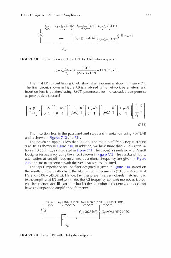
365Filter Design for RF Power Amplifiers
′ = =× ×
=L RL
3 0 6301 975
2 8 101178 7n
c
nHω π
.( )
. [ ]
The final LPF circuit having Chebyshev filter response is shown in Figure 7.9. The final circuit shown in Figure 7.9 is analyzed using network parameters, and insertion loss is obtained using ABCD parameters for the cascaded components as previously discussed:
A BC D
Z j Lj C
=
′
′
1
0 1
1
0 1
1 01
2
S ωω 11
1
0 1
1 01
13
4
′
′
′j Lj C
j Lωω
ω 55
0 1
1 01
1
ZL
(7.22)
The insertion loss in the passband and stopband is obtained using MATLAB and is shown in Figures 7.10 and 7.11.
The passband ripple is less than 0.1 dB, and the cut-off frequency is around 9 MHz, as shown in Figure 7.10. In addition, we have more than 25-dB attenua-tion at 13.56 MHz, as illustrated in Figure 7.11. The circuit is simulated with Ansoft Designer for accuracy using the circuit shown in Figure 7.12. The passband ripple, attenuation at cut-off frequency, and operational frequency are given in Figure 7.13 and are in agreement with the MATLAB results obtained.
The input impedance for the filter designed is given in Figure 7.14. Based on the results on the Smith chart, the filter input impedance is (29.58 − j8.48) Ω at F/2 and (0.06 + j43.02) Ω. Hence, the filter presents a very closely matched load to the amplifier at F/2 and terminates the F/2 frequency content; moreover, it pres-ents inductance, acts like an open load at the operational frequency, and does not have any impact on amplifier performance.
Zin
g0 = 1 L1 = g1 = 1.1468 L3 = g3 = 1.975
C2 = g2 = 1.3712 C4 = g4 = 1.3712RL = g5 = 1
L5 = g5 = 1.1468
FIGURE 7.8 Fifth-order normalized LPF for Chebyshev response.
Zin
C2 = 909.3 [pF] C2 = 909.3 [pF]
L1 = 684.44 [nH]30 [Ω] L3 = 1178.7 [nH] L1 = 684.44 [nH]
30 [Ω]
FIGURE 7.9 Final LPF with Chebyshev response.
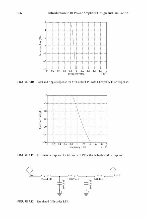
366 Introduction to RF Power Amplifier Design and Simulation
0
–1
–2
–3
–4
–5
–60 0.2 0.4 0.6 0.8 1Frequency (Hz) × 107
Inse
rtio
n lo
ss (d
B)
1.2 1.4 1.6 1.8 2
FIGURE 7.10 Passband ripple response for fifth-order LPF with Chebyshev filter response.
0
–5
–10
–15
–20
–25
–300 0.2 0.4 0.6 0.8 1Frequency (Hz) × 107
Inse
rtio
n lo
ss (d
B)
1.2 1.4 1.6 1.8 2
FIGURE 7.11 Attenuation response for fifth-order LPF with Chebyshev filter response.
Port 1 Port 2684.44 nH 1178.7 nH 684.44 nH
909.
3 pF
909.
3 pF
0 0
FIGURE 7.12 Simulated fifth-order LPF.
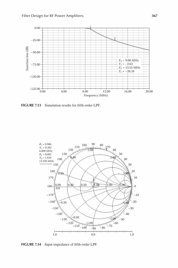
367Filter Design for RF Power Amplifiers
0.00–125.00
–120.00
–75.00
–50.00
–25.00
0.00
4.00 8.00 12.00Frequency (MHz)
Inse
rtio
n lo
ss (d
B)
16.00 20.00
2
1
X1 = 9.00 MHzY1 = –2.63X1 = 13.55 MHzY1 = –26.24
FIGURE 7.13 Simulation results for fifth-order LPF.
90
–90 –80
80 70
–70–60
6050
2.00
1.00
0.50
0.20
–0.20
–0.50–1.00
–2.00
–5.00
5.00
5.002.001.00
1
0.500.200.000.0
–50–40
4030
–30
–20
20
10
–10
0
–100
100110
–110–120
120130
–130–140
140
R1 = 0.986X1 = 0.2826.800 MHzR2 = 0.002X2 = 1.43413.550 MHz
150
–150
–160
160
170
–170
180
1.0 0.0 1.0
2
FIGURE 7.14 Input impedance of fifth-order LPF.
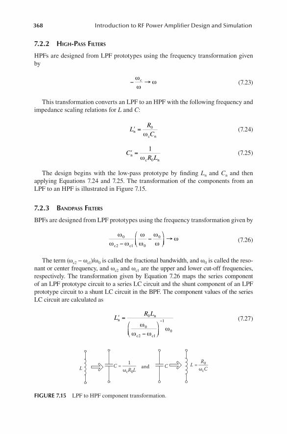
368 Introduction to RF Power Amplifier Design and Simulation
7.2.2 HigH-Pass FiLters
HPFs are designed from LPF prototypes using the frequency transformation given by
− →ωω
ωc (7.23)
This transformation converts an LPF to an HPF with the following frequency and impedance scaling relations for L and C:
′ =LRCnc n
0
ω (7.24)
′ =CR Ln
c n
1
0ω (7.25)
The design begins with the low-pass prototype by finding Ln and Cn and then applying Equations 7.24 and 7.25. The transformation of the components from an LPF to an HPF is illustrated in Figure 7.15.
7.2.3 BandPass FiLters
BPFs are designed from LPF prototypes using the frequency transformation given by
ω
ω ωωω
ωω
ω0
2 1 0
0
c c−−
→ (7.26)
The term (ωc2 − ωc1)/ω0 is called the fractional bandwidth, and ω0 is called the reso-nant or center frequency, and ωc2 and ωc1 are the upper and lower cut-off frequencies, respectively. The transformation given by Equation 7.26 maps the series component of an LPF prototype circuit to a series LC circuit and the shunt component of an LPF prototype circuit to a shunt LC circuit in the BPF. The component values of the series LC circuit are calculated as
′ =
−
−L
R Ln
n
c c
0
0
2 1
1
0ω
ω ωω
(7.27)
L1C =
ωcR0L ωcCand CR0L =
FIGURE 7.15 LPF to HPF component transformation.
369Filter Design for RF Power Amplifiers
′ =−
−
CR Ln
c c
n
ωω ω
ω
0
2 1
1
0 0 (7.28)
The component values of the shunt LC circuit are calculated as
′ =−
−
L
R
Cnc c
n
ωω ω
ω
0
2 1
1
0
0
(7.29)
′ =
−
−C
C
R
nn
c c
ωω ω
ω0
2 1
1
0 0
(7.30)
The transformation of the components from an LPF to a BPF is illustrated in Figure 7.16.
7.2.4 BandstoP FiLters
BSFs are designed from LPF prototypes using the frequency transformation given by
ω ωω
ωω
ωω
ωc c2 1
0 0
0
1−
−
→
−
(7.31)
This transformation maps the series component of an LPF prototype circuit to a shunt LC circuit and a shunt component of an LPF prototype circuit to a series LC circuit in the BSF. The component values of the shunt LC circuit are calculated as
′ =−
−
L
L R
nc c
nω
ω ω
ω
0
2 1
1
0
0 (7.32)
L andC
R0Ln–1
–1
ω0
ω0R0Ln
ω0Cn R0ω0
R0ω0ωc2 – ωc1 ω0
ωc2 – ωc1ω0
ωc2 – ωc1ω0
ωc2 – ωc1
Ln =
Ln =
Cn =
–1
–1Cn= Cn
FIGURE 7.16 LPF to BPF component transformation.
370 Introduction to RF Power Amplifier Design and Simulation
′ =
−
−C
L R
n
c cn
1
0
2 1
1
0 0ω
ω ωω
(7.33)
The component values of the series LC circuit are calculated as
′ =
−
−L
R
C
n
c cn
0
0
2 1
1
0ω
ω ωω
(7.34)
′ =
−
−
C
C
Rnc c
nω
ω ω
ω
0
2 1
1
0 0 (7.35)
The transformation of the components from an LPF to a BSF is illustrated in Figure 7.17.
7.3 STEPPED-IMPEDANCE LPFs
A stepped-impedance filter is made up of high- and low-impedance sections of trans-mission line shown in Figure 7.18. Using transmission line theory, the high- and low-impedance sections are implemented to realize LPFs.
The two-port Z-parameter matrix for a transmission line in Figure 7.18 is
ZjZ jZ
jZ jZ=
− −
− −
0 0
0 0
cot( ) csc( )
csc( ) cot( )
β β
β β
(7.36)
Land C
–1
–1
–1
–1LnR0
LnR0ω0
R0ω0
ω0
ω0ωc2 – ωc1 ω0
ωc2 – ωc1
R0
L n=C n=
C n =Cn
Cnω01
L n =ω0
ωc2 – ωc1
ω0ωc2 – ωc1
FIGURE 7.17 LPF to BSF component transformation.
ℓ
Z0β
i1 i2
v2v1
FIGURE 7.18 Transmission line model.
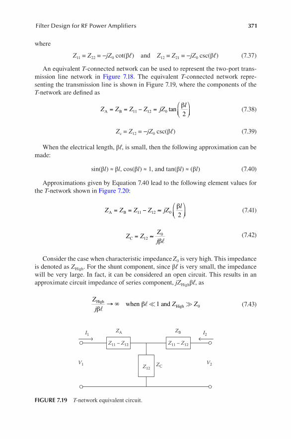
371Filter Design for RF Power Amplifiers
where
Z11 = Z22 = −jZ0 cot(βℓ) and Z12 = Z21 = −jZ0 csc(βℓ) (7.37)
An equivalent T-connected network can be used to represent the two-port trans-mission line network in Figure 7.18. The equivalent T-connected network repre-senting the transmission line is shown in Figure 7.19, where the components of the T-network are defined as
Z Z Z Z jZl
A B= = − =
11 12 0 2tan
β (7.38)
Zc = Z12 = −jZ0 csc(βℓ) (7.39)
When the electrical length, βℓ, is small, then the following approximation can be made:
sin(βl) ≈ βl, cos(βl) ≈ 1, and tan(βl) ≈ (βl) (7.40)
Approximations given by Equation 7.40 lead to the following element values for the T-network shown in Figure 7.20:
Z Z Z Z jZl
A B= = − ≈
11 12 0 2β
(7.41)
Z ZZjC = ≈12
0
β (7.42)
Consider the case when characteristic impedance Z0 is very high. This impedance is denoted as ZHigh. For the shunt component, since βℓ is very small, the impedance will be very large. In fact, it can be considered an open circuit. This results in an approximate circuit impedance of series component, jZHighβℓ, as
Z
jZ ZHighHighβ
β→ ∞ when and1 0 (7.43)
Z11 – Z12
Z12
I1
V1
I2
V2
ZA ZB
ZC
Z11 – Z12
FIGURE 7.19 T-network equivalent circuit.
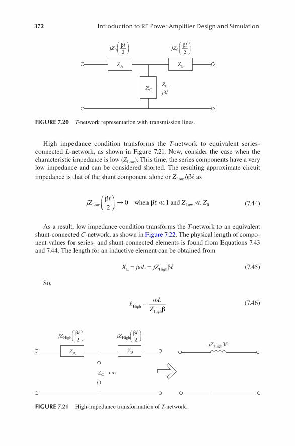
372 Introduction to RF Power Amplifier Design and Simulation
High impedance condition transforms the T-network to equivalent series-connected L-network, as shown in Figure 7.21. Now, consider the case when the characteristic impedance is low (ZLow). This time, the series components have a very low impedance and can be considered shorted. The resulting approximate circuit
impedance is that of the shunt component alone or Z jLow / β as
jZ Z ZLow Lowβ
β2
0 1 0
→ when and (7.44)
As a result, low impedance condition transforms the T-network to an equivalent shunt-connected C-network, as shown in Figure 7.22. The physical length of compo-nent values for series- and shunt-connected elements is found from Equations 7.43 and 7.44. The length for an inductive element can be obtained from
XL = jωL = jZHighβℓ (7.45)
So,
High
High
=ω
βL
Z (7.46)
ZA
βl
ZB
ZC
2βl
jβl
2jZ0 jZ0
Z0
FIGURE 7.20 T-network representation with transmission lines.
AZ BZ
2jZHigh
jZHighβℓ
βℓ βℓjZHigh 2
ZC → ∞
FIGURE 7.21 High-impedance transformation of T-network.
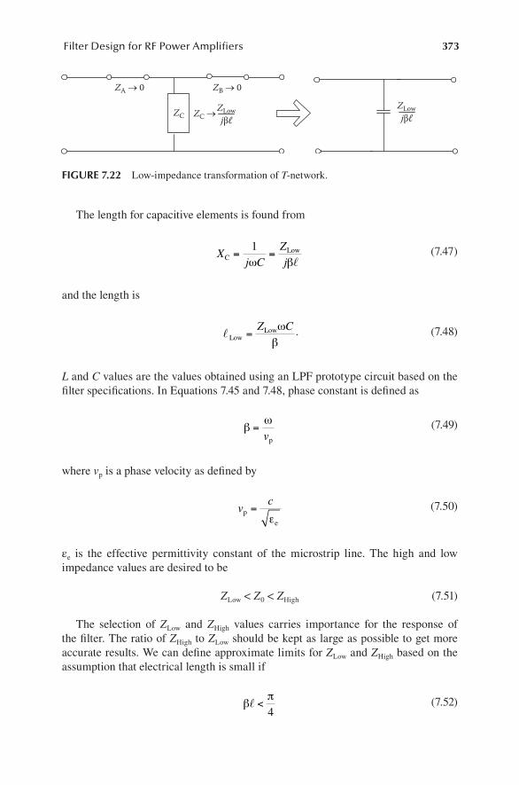
373Filter Design for RF Power Amplifiers
The length for capacitive elements is found from
Xj C
ZjCLow= =
1ω β
(7.47)
and the length is
Low
Low=Z Cω
β. (7.48)
L and C values are the values obtained using an LPF prototype circuit based on the filter specifications. In Equations 7.45 and 7.48, phase constant is defined as
βω
=vp
(7.49)
where vp is a phase velocity as defined by
vc
p
e
=ε
(7.50)
εe is the effective permittivity constant of the microstrip line. The high and low impedance values are desired to be
ZLow < Z0 < ZHigh (7.51)
The selection of ZLow and ZHigh values carries importance for the response of the filter. The ratio of ZHigh to ZLow should be kept as large as possible to get more accurate results. We can define approximate limits for ZLow and ZHigh based on the assumption that electrical length is small if
βπ
<4
(7.52)
ZA → 0 ZB → 0
ZC →ZLowjβℓ
ZLowjβℓZC
FIGURE 7.22 Low-impedance transformation of T-network.
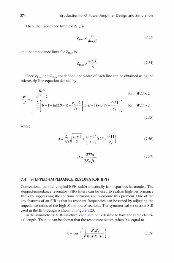
374 Introduction to RF Power Amplifier Design and Simulation
Then, the impedance limit for ZLow is
ZCLowc
<πω4
(7.53)
and the impedance limit for ZHigh is
ZL
Highc>
4ωπ
(7.54)
Once ZLow and ZHigh are defined, the width of each line can be obtained using the microstrip line equation defined by
Wd
e
eW d
B B B
=−
<
− − − +−
−
8
22
21 2 1
12
1
2
A
A
r
r
for /
πεε
ln( ) ln( )) ..
+ −
>
0 390 61
2εr
for W d/
(7.55)
where
AZ
=+
+−+
+
0
601
211
0 230 11ε ε
ε εr r
r r
..
(7.56)
BZ
=377
2 0
π
εr (7.57)
7.4 STEPPED-IMPEDANCE RESONATOR BPFs
Conventional parallel-coupled BPFs suffer drastically from spurious harmonics. The stepped-impedance resonator (SIR) filters can be used to realize high-performance BPFs by suppressing the spurious harmonics to overcome this problem. One of the key features of an SIR is that its resonant frequencies can be tuned by adjusting the impedance ratios of the high-Z and low-Z sections. The symmetrical tri-section SIR used in the BPF design is shown in Figure 7.23.
In the symmetrical SIR structure, each section is desired to have the same electri-cal length. Then, it can be shown that the resonance occurs when θ is equal to
θ =+ +
−tan 1 1 2
1 2 1K K
K K (7.58)
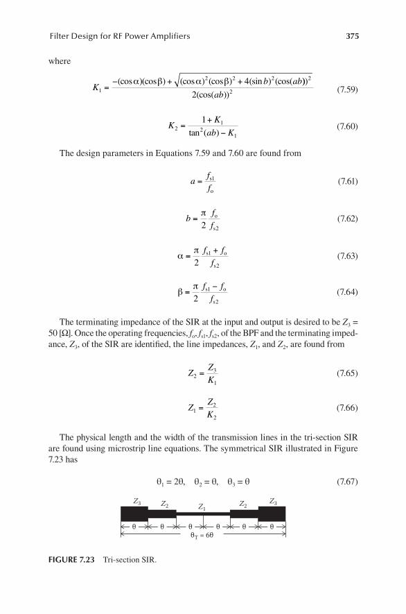
375Filter Design for RF Power Amplifiers
where
Kb ab
1
2 2 24=− + +(cos )(cos ) (cos ) (cos ) (sin ) (cos(α β α β )))
(cos( ))
2
22 ab (7.59)
KK
ab K2
12
1
1=
+
−tan ( ) (7.60)
The design parameters in Equations 7.59 and 7.60 are found from
aff
= s
o
1 (7.61)
bff
=π2 2
o
s
(7.62)
απ
=+
21
2
f ff
s o
s
(7.63)
βπ
=−
21
2
f ff
s o
s
(7.64)
The terminating impedance of the SIR at the input and output is desired to be Z3 = 50 [Ω]. Once the operating frequencies, fo, fs1, fs2, of the BPF and the terminating imped-ance, Z3, of the SIR are identified, the line impedances, Z1, and Z2, are found from
ZZK2
3
1
= (7.65)
ZZK1
2
2
= (7.66)
The physical length and the width of the transmission lines in the tri-section SIR are found using microstrip line equations. The symmetrical SIR illustrated in Figure 7.23 has
θ1 = 2θ, θ2 = θ, θ3 = θ (7.67)
θ θ θ θθT = 6θ
Z1Z2 Z2
Z3Z3
θ θ
FIGURE 7.23 Tri-section SIR.
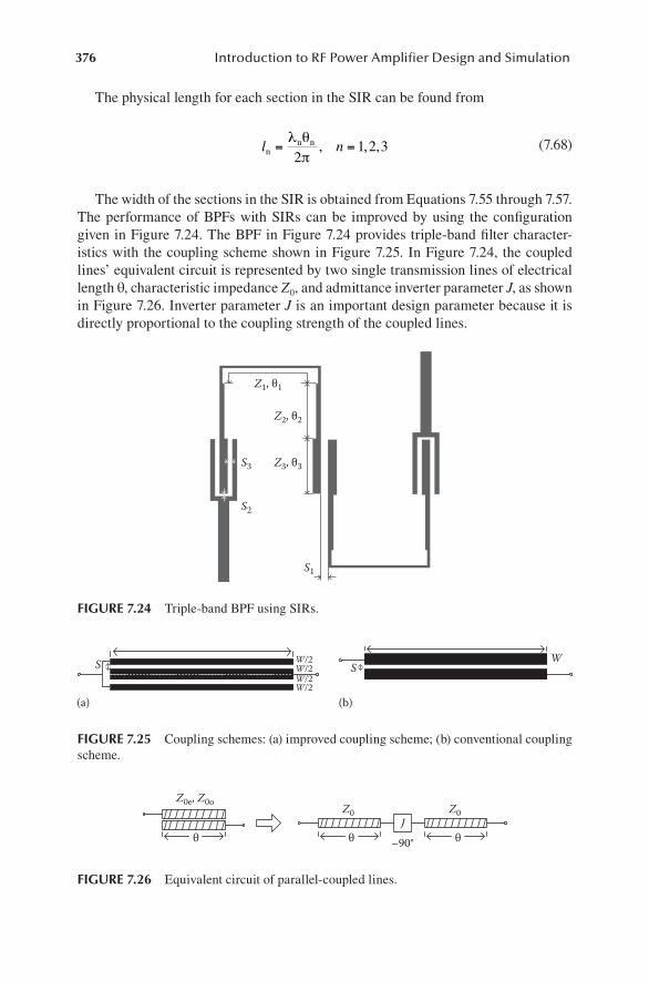
376 Introduction to RF Power Amplifier Design and Simulation
The physical length for each section in the SIR can be found from
l nnn n= =
λ θπ2
1 2 3, , , (7.68)
The width of the sections in the SIR is obtained from Equations 7.55 through 7.57. The performance of BPFs with SIRs can be improved by using the configuration given in Figure 7.24. The BPF in Figure 7.24 provides triple-band filter character-istics with the coupling scheme shown in Figure 7.25. In Figure 7.24, the coupled lines’ equivalent circuit is represented by two single transmission lines of electrical length θ, characteristic impedance Z0, and admittance inverter parameter J, as shown in Figure 7.26. Inverter parameter J is an important design parameter because it is directly proportional to the coupling strength of the coupled lines.
Z1, θ1
Z2, θ2
Z3, θ3S3
S2
S1
FIGURE 7.24 Triple-band BPF using SIRs.
Z0e, Z0o
θ θ θ
Z0 Z0J
–90°
FIGURE 7.26 Equivalent circuit of parallel-coupled lines.
S W/2W/2W/2W/2
WS
(a) (b)
FIGURE 7.25 Coupling schemes: (a) improved coupling scheme; (b) conventional coupling scheme.
377Filter Design for RF Power Amplifiers
This parameter is found using network synthesis from the equivalent circuit and is given by
J Ykg g01 0
0
0 1
2=
θ (7.69)
J Yk
g gj j
j j
, +
+
=1 00
1
2 θ (7.70)
J Y
kg gn nn n
, ++
=1 00
1
2 θ (7.71)
As the ratio J/Y between the coupled lines increases, the coupling strength also increases.
7.5 EDGE/PARALLEL-COUPLED, HALF-WAVELENGTH RESONATOR BPFs
A parallel-coupled, half-wavelength BPF is shown in Figure 7.27. For a filter of order n, there are n + 1 couplings between half-wavelength resonators. The first step of the design begins with finding the low-pass prototype circuit component values.
Then, the low-pass prototype filter undergoes transformations to have the desired BPF characteristics, as described in Section 7.2.3. To configure the circuit in a par-allel microstrip implementation, the filter must first be represented as a series of cascaded J inverters. The equations to perform this are given by
JY
FBWg g
01
0 0 12=
π (7.72)
J
YFBW
g gj nj j
j j
for to, +
+
= = −1
0 12
11 1
π (7.73)
J
YFBWg g
n n
n n
, +
+
=1
0 12π
(7.74)
where g0 − gn are the normalized impedance elements of the low-pass prototype filter, the FBW is the fractional bandwidth of the filter of 15%, and Y0 is the characteristic admittance. These coefficients can be calculated in MATLAB. The next important step in the filter design is to calculate the even- and odd-mode impedance values for the
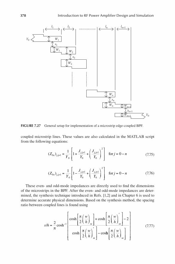
378 Introduction to RF Power Amplifier Design and Simulation
coupled microstrip lines. These values are also calculated in the MATLAB script from the following equations:
( ) ,, ,Z
Y
J
Y
J
Y0 10
1
0
1
0
21
1e j jj j j j
++ += + +
= −for j 0 n (7.75)
( ) ,, ,Z
Y
J
Y
J
Y0 10
1
0
1
0
21
1o j jj j j j
++ += − +
= −for j n0 (7.76)
These even- and odd-mode impedances are directly used to find the dimensions of the microstrips in the BPF. After the even- and odd-mode impedances are deter-mined, the synthesis technique introduced in Refs. [1,2] and in Chapter 6 is used to determine accurate physical dimensions. Based on the synthesis method, the spacing ratio between coupled lines is found using
s h
wh
wh
/ =
+
−2 2 21
π
π π
cosh
cosh coshse
′
−
′
−
so
se
2
2cosh cos
π wh
hhπ2
wh
se
(7.77)
W1
l1 l2 ln ln+1
W2W1
s1
W2
Wn
Wn
sn
s2
Wn+1
Wn+1
sn+1Y0
Y0
FIGURE 7.27 General setup for implementation of a microstrip edge-coupled BPF.
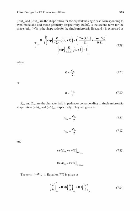
379Filter Design for RF Power Amplifiers
(w/h)se and (w/h)so are the shape ratios for the equivalent single case corresponding to even-mode and odd-mode geometry, respectively. ( )w h/ so′ is the second term for the shape ratio. (w/h) is the shape ratio for the single microstrip line, and it is expressed as
wh
R
=
+
−
++
+8
42 41 1
7 411
1/exp
.( )
( )ε
εr
r (( ).
exp.
10 81
42 41 1
/ε
ε
r
rR
+
−
(7.78)
where
RZ
= 0e
2 (7.79)
or
RZ
= 0o
2 (7.80)
Z0se and Z0so are the characteristic impedances corresponding to single microstrip shape ratios (w/h)se and (w/h)so, respectively. They are given as
ZZ
0se0e=2
(7.81)
ZZ
0so0o=2
(7.82)
and
( ) ( )w h w h
R Z/ /se
0se=
= (7.83)
( ) ( )w h w h
R Z/ /so
0so=
=
The term ( )w h/ ′so in Equation 7.77 is given as
wh
wh
wh
′=
+
so so se
0 78 0 1. . (7.84)

380 Introduction to RF Power Amplifier Design and Simulation
After the spacing ratio s/h for the coupled lines is found, we can proceed to find w/h for the coupled lines. The shape ratio for the coupled lines is
wh
dsh
= −
−1 1
21
πcosh ( ) (7.85)
where
d
wh
g g
=
+ + −cosh ( )π2
1 1
2se (7.86)
gsh
=
cosh
π2
(7.87)
The physical length of the directional coupler is obtained using
lc
f= =λ
ε4 4 eff
(7.88)
The calculation of effective permittivity constant using odd-mode and even-mode capacitances is detailed in Refs. [1,2].
Design Example
Design and simulate a fifth-order, edge-coupled, half-wavelength resonator BPF with 0.1-dB passband ripple, fC = 10 GHz, εr = 10.2, FBW = 0.15, and dielectric thickness of 0.635 mm.
Solution
The first step is to design the low-pass Chebyshev prototype filter coefficients. They are determined from the design table (Figure 7.7) and are shown in Figure 7.28. The filter coefficients are
g0 = 1 = g6, g1 = 1.1468 = g5, g2 = 1.3712 = g4, g3 = 1.9750
The prototype circuit is then transformed into the equivalent BPF using the trans-formation circuits given in Figure 7.16. The BPF with the final component values is illustrated in Figure 7.29. The frequency response of the filter is simulated with Ansoft Designer, and the insertion and return losses are given in Figure 7.30.
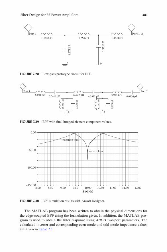
381Filter Design for RF Power Amplifiers
The MATLAB program has been written to obtain the physical dimensions for the edge-coupled BPF using the formulation given. In addition, the MATLAB pro-gram is used to obtain the filter response using ABCD two-port parameters. The calculated inverter and corresponding even-mode and odd-mode impedance values are given in Table 7.3.
Port 1 Port 1_21.1468 H 1.975 H 1.1468 H
1.37
12 F
1.37
12 F
0 0
FIGURE 7.28 Low-pass prototype circuit for BPF.
Port 16.084 nH 60.439 pH 6.084 nH 0.0416 pF4.1911 pF0.0416 pF
87.0
52 p
H
2.90
98 p
F
87.0
52 p
H
2.90
98 p
F
Port 2
00
FIGURE 7.29 BPF with final lumped element component values.
0.00
–50.00
–100.00
–150.008.00 8.50 9.00 9.50
Insertion loss
Return loss
10.00F (GHz)
10.50 11.00 12.0011.50
FIGURE 7.30 BPF simulation results with Ansoft Designer.

382 Introduction to RF Power Amplifier Design and Simulation
The generic MATLAB script that is used to obtain the lumped-element BPF fre-quency response and physical dimensions of the edge-coupled filter is given below.
% Edge Coupled Bandpass Filter Design Programclcclear;close all;
Z0 = 50; % Charac. Impedancefc = 10e9; % Operational frequencyEr = 10.2; % Rel Perm of the dielectricBW = .15; % Bandwidth Percentageh = 0.635e-3; % Thickness of the dielectricn = 5; % Order of the Filter c = 3e8; % speed of light eps0=8.85e-12;
g(1) = 1.1468;g(2) = 1.3712;g(3) = 1.975;g(4) = 1.3712;g(5) = 1.1468;g(6) = 1.0000;
% Conversion from LPF Prototype to BPF EquivalentLs1 = (Z0*g(1))/(BW*2*pi*fc);Ls5 = Ls1;Cs1 = BW/(g(1)*Z0*2*pi*fc);Cs5 = Cs1;Lp2 = (BW*Z0)/(2*pi*fc*g(2));Cp2 = g(2)/(Z0*BW*2*pi*fc);Lp4 = Lp2;Cp4 = Cp2;Ls3 = (BW*Z0)/(2*pi*fc*g(3));Cs3 = g(3)/(Z0*BW*2*pi*fc);Z0J(1) = sqrt((pi*BW)/(2*g(1)));
TABLE 7.3Even- and Odd-Mode Impedance Values
j Jj,j+1 (Z0e)j,j+1 (Z0o)j,j+1
0 0.4533 82.9367 37.6092
1 0.1879 61.1600 42.3705
2 0.1432 58.1839 43.8661
3 0.1432 58.1839 43.8661
4 0.1879 61.1600 42.3705
5 0.4533 82.9367 37.6092

383Filter Design for RF Power Amplifiers
% J Inverter Calculationfor i=1:n-1 Z0J(i+1) = ((pi*BW)/2)*(1/(sqrt(g(i)*g(i+1))));endZ0J(n+1) = sqrt((pi*BW)/(2*g(n)*g(n+1)));
for i=0:1:n Z0e(i+1) = Z0*((1+Z0J(i+1)+Z0J(i+1)^2)); Z0o(i+1) = Z0*((1-Z0J(i+1)+Z0J(i+1)^2));end for i=1:n+1
% the shape ratio for the equivalent single microstrip correspond to even mode% whse(i)=8*sqrt((exp(Z0e(i)/2/42.4*sqrt(Er+1))-1)*(7+4/Er)/11+(1+1/Er)/0.81)/(exp(Z0e(i)/2/42.4*sqrt(Er+1))-1);% the shape ratio for the equivalent single microstrip correspond to odd mode%whso(i)=8*sqrt((exp(Z0o(i)/2/42.4*sqrt(Er+1))-1)*(7+4/Er)/11+(1+1/Er)/0.81)/(exp(Z0o(i)/2/42.4*sqrt(Er+1))-1);whso1(i)=0.78*whso(i)+0.1*whse(i);
% space ratio of coupled lines %sh(i)=(2/pi)*acosh((cosh(pi/2*whse(i))+cosh(pi/2*whso1(i))-2)/(cosh(pi/2*whso1(i))-cosh(pi/2*whse(i)))); g(i)=cosh((pi/2)*sh(i));d(i)=(cosh((pi/2)*whse(i))*(g(i)+1)+(g(i)-1))/2;% shape ratio of coupled lines %wh(i)=(1/pi)*acosh(d(i))-0.5*(sh(i));
%Calculate the even mode capacitanceif wh(i)<=1 F(i)=(1+(12/wh(i)))^(-0.5)+0.041*(1-wh(i))^2;else F(i)=(1+(12/wh(i)))^(-0.5);endCp(i)=eps0*Er*wh(i);epseffs(i)=(Er+1)/2+((Er-1)/2)*F(i);Cf(i)=sqrt(epseffs(i))/(2*c*Z0)-Cp(i)/2;A(i)=exp(-0.1*exp(2.33-1.5*wh(i)));Cf1(i)=(Cf(i)/(1+(A/sh)*tanh(10*sh(i))))*(Er/epseffs(i))^0.25;Ce(i)=Cp(i)+Cf(i)+Cf1(i);
%Calculate the odd mode capacitancek(i)=sh(i)/(sh(i)+2*wh(i));k1(i)=k(i)^2;k2(i)=sqrt(1-k1(i));if k1(i)<=0.5 K(i)=(1/pi)*log(2*(1+sqrt(k2(i)))/(1-sqrt(k2(i))));else

384 Introduction to RF Power Amplifier Design and Simulation
K(i)=(pi)/log(2*(1+sqrt(k2(i)))/(1-sqrt(k2(i))));end
Cga(i)=eps0*K(i);Cgd(i)=((eps0*Er)/(pi))*log(coth((pi/4)*sh(i)))+0.65*Cf(i)*((0.02*sqrt(Er)/sh(i))+(1-1/(Er)^2));Co(i)=Cp(i)+Cf(i)+Cga(i)+Cgd(i);
%Calculation of effective permittivity constant
Ce1(i)=1/((c^2)*Ce(i)*(Z0e(i))^2);Co1(i)=1/((c^2)*Co(i)*(Z0o(i))^2);epseffe(i)=Ce(i)/Ce1(i);epseffo(i)=Co(i)/Co1(i);epseff(i)=((sqrt(epseffe(i))+sqrt(epseffo(i)))/2)^2;
%Calculation of length of coupler linel(i)=(c/(4*fc*sqrt(epseff(i))))*1000; %in mm
end
freq=8e9:0.0001e9:12e9;[M,N]=size(freq);j=sqrt(-1);
for k=1:1:N f=freq(M,k);
% ABCD parameters of Each Component at each frequency Zmatrix_Ls1 = [1 (2j*pi*f*Ls1);0 1]; Zmatrix_Ls5 = Zmatrix_Ls1; Zmatrix_Cs1 = [1 (-j/(2*pi*f*Cs1));0 1]; Zmatrix_Cs5 = Zmatrix_Cs1; Zmatrix_Lp2 = [1 0;(-j/(2*pi*f*Lp2)) 1]; Zmatrix_Lp4 = Zmatrix_Lp2; Zmatrix_Cp2 = [1 0;(2j*pi*f*Cp2) 1]; Zmatrix_Cp4 = Zmatrix_Cp2; Zmatrix_Ls3 = [1 (2j*pi*f*Ls3);0 1]; Zmatrix_Cs3 = [1 (-j/(2*pi*f*Cs3));0 1];
% ABCD Parameter Conversion ABCD=Zmatrix_Ls1*Zmatrix_Cs1*Zmatrix_Lp2*Zmatrix_Cp2*Zmatrix_Ls3*Zmatrix_Cs3*Zmatrix_Lp4*Zmatrix_Cp4*Zmatrix_Ls5*Zmatrix_Cs5;
A=ABCD(1,1); B=ABCD(1,2); C=ABCD(2,1); D=ABCD(2,2);

385Filter Design for RF Power Amplifiers
S11(k)=(A+(B/Z0)-(C*Z0)-D)/(A+(B/Z0)+(C*Z0)+D); S21(k)=2/(A+(B/Z0)+(C*Z0)+D);end
fprintf ('Bandpass Filter Lumped Element Component Values : \n Ls1=% 0.5e\nLs5=% 0.5e\nCs1=% 0.5e\nCs5=%... 0.5e\nLp2=% 0.5e\nCp2=% 0.5e\nLp4=% 0.5e\nCp4=% 0.5e\nLs3=% 0.5e\nCs3=%... 0.5e\n\n',Ls1,Ls5,Cs1,Cs5,Lp2,Cp2,Lp4,Cp4,Ls3,Cs3); fprintf('\nInverter Values... :\nZ0J(1)=%0.4f\nZ0J(2)=%0.4f\nZ0J(3)=%0.4f\nZ0J(4)=%0.4f\nZ0J(5)=%0.4f\nZ0J(6)=%0.4f\n\n',...Z0J(1),Z0J(2),Z0J(3),Z0J(4),Z0J(5),Z0J(6));fprintf('Even-mode impedance Z0e:\nZ0e(1)= %0.4f\nZ0e(2)= %0.4f\nZ0e(3)= %0.4f \nZ0e(4)= %0.4f \n...Z0e(5)= %0.4f \nZ0e(6)= %0.4f\n\n',Z0e(1),Z0e(2),Z0e(3),Z0e(4),Z0e(5),Z0e(6));fprintf('Odd-mode impedance Z0o:\nZ0o(1)= %0.4f\nZ0o(2)= %0.4f\nZ0o(3)= %0.4f \nZ0o(4)= %0.4f \n...Z0o(5)= %0.4f \nZ0o(6)= %0.4f\n\n',Z0o(1),Z0o(2),Z0o(3),Z0o(4),Z0o(5),Z0o(6));fprintf ('\nEffective Dielectric Coefficient:\n');fprintf ('epseff(1)=% 0.4f\n epseff(2)=% 0.4f\n epseff(3)=% 0.4f\n epseff(4)=% 0.4f\n epseff(5)=% 0.4f\n... epseff(6)=% 0.4f\n\n',epseff(1),epseff(2),epseff(3),epseff(4),epseff(5),epseff(6));fprintf ('\nSpacing Ratio for Edge Coupled Microstrip Lines:\n') ;fprintf ('s/h(1)=% 0.4f\ns/h(2)=% 0.4f\ns/h(3)=% 0.4f\ns/h(4)=% 0.4f\ns/h(5)=% 0.4f\ns/h(6)=%... 0.4f\n',sh(1),sh(2),sh(3),sh(4),sh(5),sh(6)); fprintf ('\nShape Ratio for Edge Coupled Microstrip Lines:\n');fprintf ('w/h(1)=% 0.4f\nw/h(2)=% 0.4f\nw/h(3)=% 0.4f\nw/h(4)=% 0.4f\nw/h(5)=% 0.4f\nw/h(6)=%... 0.4f\n\n',wh(1),wh(2),wh(3),wh(4),wh(5),wh(6)); fprintf ('Electrical Length (m):\n');fprintf ('l(1)=% 0.5f\n l(2)=% 0.5f\n l(3)=% 0.5f\n l(4)=% 0.5f\n l(5)=% 0.5f\n ...l(6)=% 0.5f\n\n',l(1),l(2),l(3),l(4),l(5),l(6));
figureplot(freq*1e-9,20*log10(abs(S11)),'-mo',freq*1e-9,20*log10(abs(S21)),'bx')h = legend('S_11(dB)','S_21(dB)',2);title('\bfReturn Loss and Insertion Loss vs Frequency(GHz)')grid onxlabel('Frequency (GHz)')ylabel('S_11(dB) & S_21(dB)')axis([8 12 -100 0]);
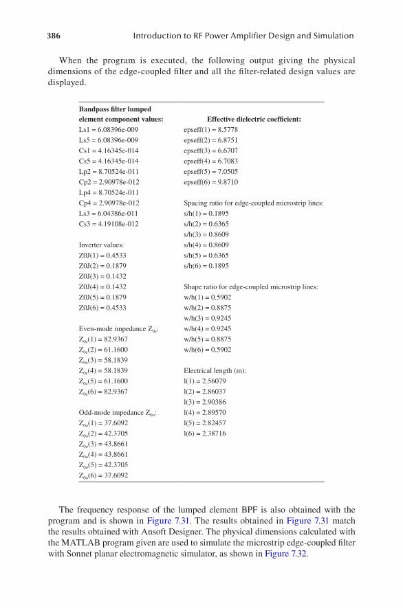
386 Introduction to RF Power Amplifier Design and Simulation
When the program is executed, the following output giving the physical dimensions of the edge-coupled filter and all the filter-related design values are displayed.
Bandpass filter lumpedelement component values: Effective dielectric coefficient:Ls1 = 6.08396e-009 epseff(1) = 8.5778
Ls5 = 6.08396e-009 epseff(2) = 6.8751
Cs1 = 4.16345e-014 epseff(3) = 6.6707
Cs5 = 4.16345e-014 epseff(4) = 6.7083
Lp2 = 8.70524e-011 epseff(5) = 7.0505
Cp2 = 2.90978e-012 epseff(6) = 9.8710
Lp4 = 8.70524e-011
Cp4 = 2.90978e-012 Spacing ratio for edge-coupled microstrip lines:
Ls3 = 6.04386e-011 s/h(1) = 0.1895
Cs3 = 4.19108e-012 s/h(2) = 0.6365
s/h(3) = 0.8609
Inverter values: s/h(4) = 0.8609
Z0J(1) = 0.4533 s/h(5) = 0.6365
Z0J(2) = 0.1879 s/h(6) = 0.1895
Z0J(3) = 0.1432
Z0J(4) = 0.1432 Shape ratio for edge-coupled microstrip lines:
Z0J(5) = 0.1879 w/h(1) = 0.5902
Z0J(6) = 0.4533 w/h(2) = 0.8875
w/h(3) = 0.9245
Even-mode impedance Z0e: w/h(4) = 0.9245
Z0e(1) = 82.9367 w/h(5) = 0.8875
Z0e(2) = 61.1600 w/h(6) = 0.5902
Z0e(3) = 58.1839
Z0e(4) = 58.1839 Electrical length (m):
Z0e(5) = 61.1600 l(1) = 2.56079
Z0e(6) = 82.9367 l(2) = 2.86037
l(3) = 2.90386
Odd-mode impedance Z0o: l(4) = 2.89570
Z0o(1) = 37.6092 l(5) = 2.82457
Z0o(2) = 42.3705 l(6) = 2.38716
Z0o(3) = 43.8661
Z0o(4) = 43.8661
Z0o(5) = 42.3705
Z0o(6) = 37.6092
The frequency response of the lumped element BPF is also obtained with the program and is shown in Figure 7.31. The results obtained in Figure 7.31 match the results obtained with Ansoft Designer. The physical dimensions calculated with the MATLAB program given are used to simulate the microstrip edge-coupled filter with Sonnet planar electromagnetic simulator, as shown in Figure 7.32.
387Filter Design for RF Power Amplifiers
The Sonnet simulation results are illustrated in Figure 7.33. Since the material properties are entered, the simulation results are slightly different than the ideal results obtained using lumped elements by Ansoft and MATLAB. Overall, the inser-tion loss requirement, center frequency, and attenuation profile for edge-coupled fil-ter are achieved with the method used.
7.6 END-COUPLED, CAPACITIVE GAP, HALF- WAVELENGTH RESONATOR BPFs
The general configuration of an end-coupled microstrip BPF is shown in Figure 7.34.The gap between two adjacent open ends is capacitive and can be represented
by inverters. J-inverters tend to reflect high impedance levels to the ends of each
0
–10
–20
–30
–40
–50
–60
–70
–80
–90
–1008 8.5 9.59 10.510Frequency (GHz)
S 11 (
dB) a
nd S
21 (d
B)
Return loss and insertion loss vs. frequency (GHz)
11.511 12
S11 (dB)S21 (dB)
FIGURE 7.31 BPF simulation results with MATLAB.
2
1
FIGURE 7.32 Simulated edge-coupled microstrip circuit with Sonnet.
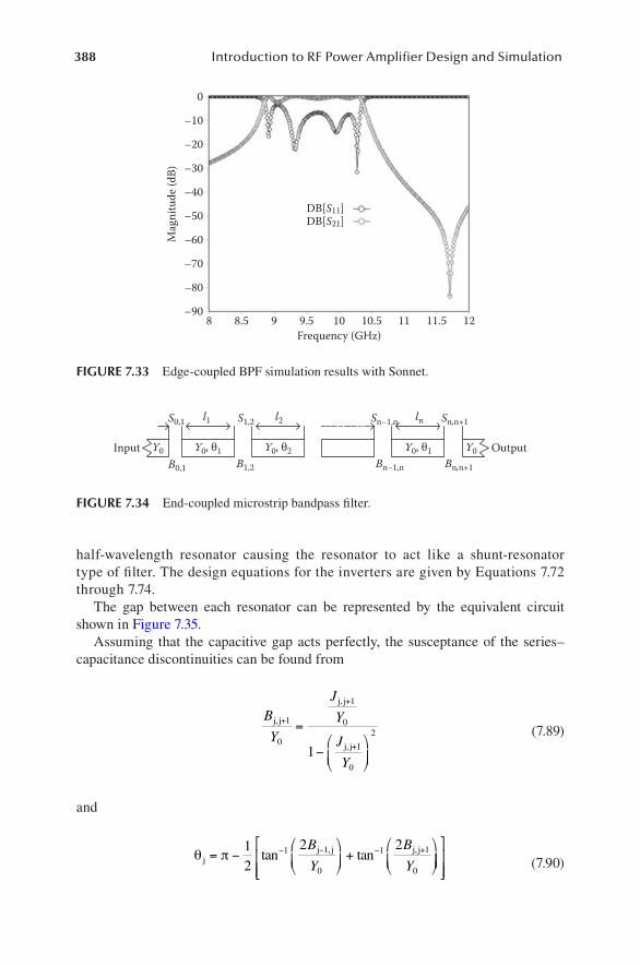
388 Introduction to RF Power Amplifier Design and Simulation
half-wavelength resonator causing the resonator to act like a shunt-resonator type of filter. The design equations for the inverters are given by Equations 7.72 through 7.74.
The gap between each resonator can be represented by the equivalent circuit shown in Figure 7.35.
Assuming that the capacitive gap acts perfectly, the susceptance of the series–capacitance discontinuities can be found from
B
Y
J
Y
J
Y
j j
j j
j j
,
,
,
+
+
+
=
−
1
0
1
0
1
0
2
1
(7.89)
and
θ πjj j j j= −
+
− − − +1
2
2 21 1
0
1 1
0
tan tan, ,B
Y
B
Y
(7.90)
0
–10
–20
–30
–40
–50
–60
–70
–80
–908 8.5 9 9.5 10
DB[S11]DB[S21]
Frequency (GHz)
Mag
nitu
de (d
B)
10.5 11 1211.5
FIGURE 7.33 Edge-coupled BPF simulation results with Sonnet.
Y0, θ1Y0Input
l1 l2 ln
Y0 OutputB0,1
S0,1 S1,2 Sn–1,n Sn,n+1
B1,2 Bn–1,n Bn,n+1
Y0, θ2 Y0, θ1
FIGURE 7.34 End-coupled microstrip bandpass filter.
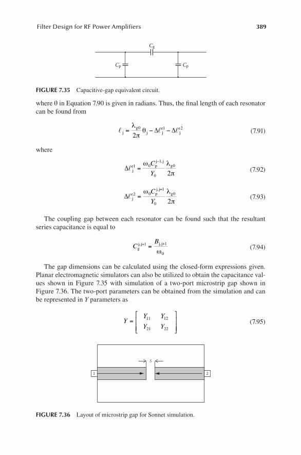
389Filter Design for RF Power Amplifiers
where θ in Equation 7.90 is given in radians. Thus, the final length of each resonator can be found from
jg
j je
je∆ ∆= − −
λ
πθ0 1 2
2 (7.91)
where
∆ je p
j jg1 0
1
0
0
2=
−ω λ
π
C
Y
,
(7.92)
∆ je p
j jg2 0
1
0
0
2=
+ω λ
π
C
Y
,
(7.93)
The coupling gap between each resonator can be found such that the resultant series capacitance is equal to
CB
gj j j j, ,+ +=1 1
0ω (7.94)
The gap dimensions can be calculated using the closed-form expressions given. Planar electromagnetic simulators can also be utilized to obtain the capacitance val-ues shown in Figure 7.35 with simulation of a two-port microstrip gap shown in Figure 7.36. The two-port parameters can be obtained from the simulation and can be represented in Y parameters as
Y
Y Y
Y Y= 11 12
21 22 (7.95)
Cg
Cp Cp
FIGURE 7.35 Capacitive-gap equivalent circuit.
1 2
S
FIGURE 7.36 Layout of microstrip gap for Sonnet simulation.
390 Introduction to RF Power Amplifier Design and Simulation
Using the simulated Y parameters, the following capacitance values are obtained:
CY
g = −Im( )21
0ω (7.96)
CY Y
p = −+Im( )11 21
0ω (7.97)
Design Example
Design and simulate an end-coupled, capacitive-gap microstrip BPF with the order of n = 3 0.1-dB passband ripple. The center frequency of the filter is at 6 GHz, and the filter has to meet a bandwidth requirement of 2.8%. The filter has to be inserted into 50-Ω characteristic line impedance. For the microstrip imple-mentation, it is given that the dielectric constant is εr = 10.8, the thickness of the substrate is 1.27 mm, and the width is 1.1 mm.
Solution
The equivalent circuit of the BPF is derived through the use of the LPF prototype illustrated in Figure 7.37. The ABCD parameters of the entire network are found from cascading the ABCD parameters of each circuit component. The frequency response of the filter is obtained from converting the network ABCD parameters to scattered parameters.
The Chebyshev filter prototype values are determined from the design in Figure 7.7 [1]. The normalized component values of the filter are
g0 = g4 = 1.0, g1 = g3 = 1.0316, and g2 = 1.1474
The LPF prototype illustrated in Figure 7.1 is used to design the equivalent circuit for the BPF. The low-pass prototype filter is converted to a BPF shown in Figure 7.38 with application of the transformation circuits given in Figure 7.16.
G0 = g0 = 1 C2 = g2 Gn + 1
L3 = g3L1 = g1
FIGURE 7.37 LPF prototype.
391Filter Design for RF Power Amplifiers
In order to determine the ABCD parameters of the overall network, the ABCD parameters of each component can be cascaded. To obtain the frequency response of the filter, the ABCD parameters are converted into scattered parameters as
A BC D
j Lj C
=
′
′
1
0 1
11
0 1
1ω
ωss
001
11 0
11
0 1j Lj C
j L
ωω
ω
′
′
′
pp
s
′
11
0 1
j Cω s
(7.98)
S S
S S
ABZ
CZ DAD BC
11 12
21 22
00
7 7
7
2
2
=
+ − +−
ψ ψ
ψ
( )
−− + − +
ABZ
CZ D0
0
7ψ
(7.99)
where
ψ70
0= + + +ABZ
CZ D (7.100)
Insertion and return losses can be obtained from S21. The final component values of the filter are calculated and shown in Figure 7.39.
The insertion and return losses are obtained using MATLAB and are shown in Figure 7.40. The MATLAB script is given below.
%Bandpass filter response with equivalent circuitZ0 = 50;FBW = .028;f0 = 6*10^(9);w0 = 2*pi*f0;f = [5.4e9:10e6:6.6e9];%5.4e9syms x;w = 2*pi*x;
+
Rs
RlL´ C´
L´ L´C´ C´
–
FIGURE 7.38 Equivalent circuit BPF.
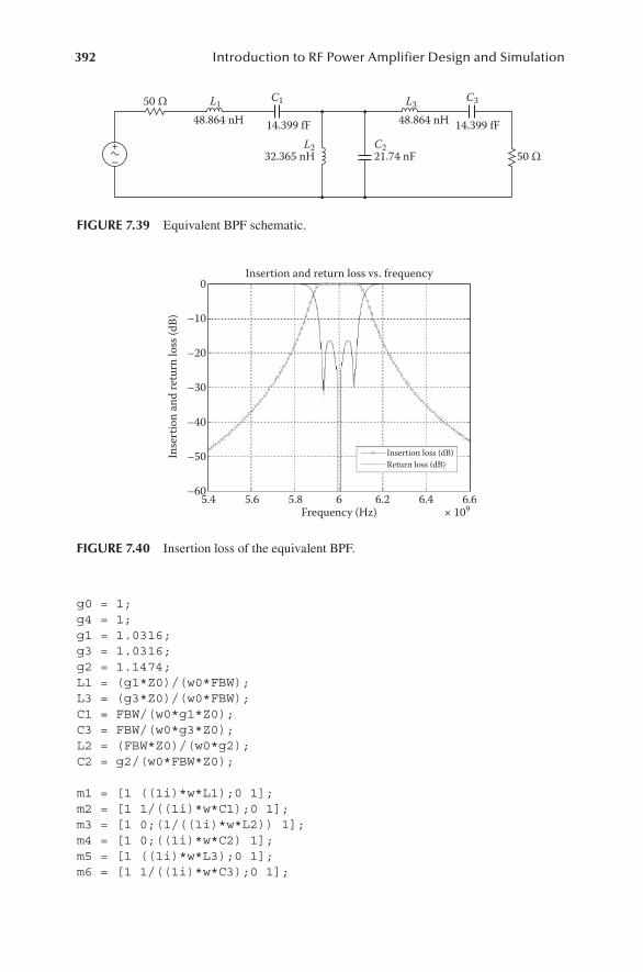
392 Introduction to RF Power Amplifier Design and Simulation
g0 = 1;g4 = 1;g1 = 1.0316;g3 = 1.0316;g2 = 1.1474;L1 = (g1*Z0)/(w0*FBW);L3 = (g3*Z0)/(w0*FBW);C1 = FBW/(w0*g1*Z0);C3 = FBW/(w0*g3*Z0);L2 = (FBW*Z0)/(w0*g2);C2 = g2/(w0*FBW*Z0);
m1 = [1 ((1i)*w*L1);0 1];m2 = [1 1/((1i)*w*C1);0 1];m3 = [1 0;(1/((1i)*w*L2)) 1];m4 = [1 0;((1i)*w*C2) 1];m5 = [1 ((1i)*w*L3);0 1];m6 = [1 1/((1i)*w*C3);0 1];
+
50 Ω
50 Ω
48.864 nH 48.864 nH14.399 fF 14.399 fFL2
32.365 nHC221.74 nF
L1 L3C1 C3
–
FIGURE 7.39 Equivalent BPF schematic.
0
–10
–20
–30
–40
–50
–605.4 5.6 5.8 6
Frequency (Hz)
Inse
rtio
n an
d re
turn
loss
(dB)
Insertion and return loss vs. frequency
× 1096.2 6.4 6.6
Insertion loss (dB)Return loss (dB)
FIGURE 7.40 Insertion loss of the equivalent BPF.
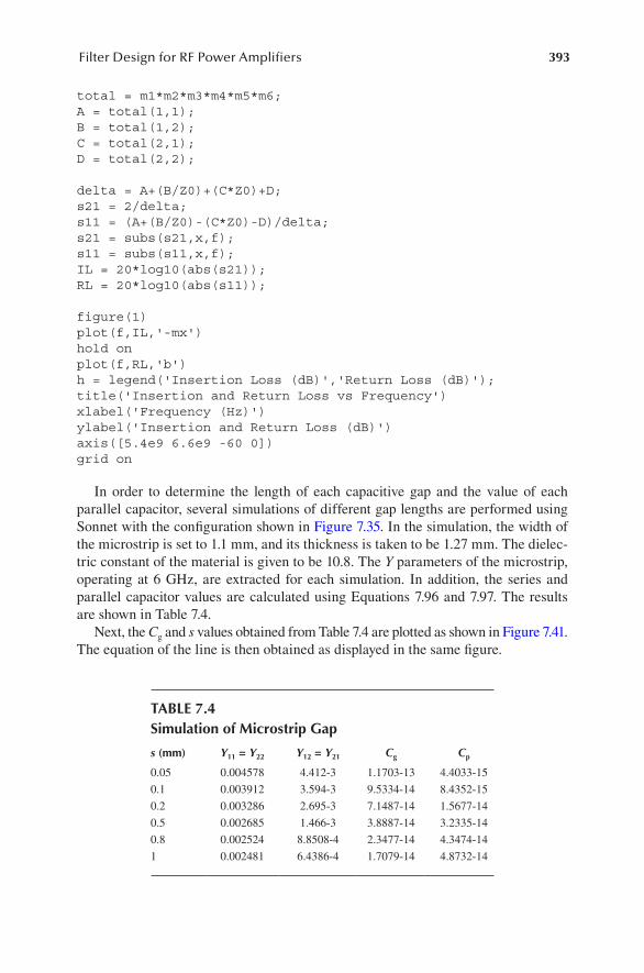
393Filter Design for RF Power Amplifiers
total = m1*m2*m3*m4*m5*m6;A = total(1,1);B = total(1,2);C = total(2,1);D = total(2,2);
delta = A+(B/Z0)+(C*Z0)+D;s21 = 2/delta;s11 = (A+(B/Z0)-(C*Z0)-D)/delta;s21 = subs(s21,x,f);s11 = subs(s11,x,f);IL = 20*log10(abs(s21));RL = 20*log10(abs(s11));
figure(1)plot(f,IL,'-mx')hold onplot(f,RL,'b')h = legend('Insertion Loss (dB)','Return Loss (dB)');title('Insertion and Return Loss vs Frequency')xlabel('Frequency (Hz)')ylabel('Insertion and Return Loss (dB)')axis([5.4e9 6.6e9 -60 0])grid on
In order to determine the length of each capacitive gap and the value of each parallel capacitor, several simulations of different gap lengths are performed using Sonnet with the configuration shown in Figure 7.35. In the simulation, the width of the microstrip is set to 1.1 mm, and its thickness is taken to be 1.27 mm. The dielec-tric constant of the material is given to be 10.8. The Y parameters of the microstrip, operating at 6 GHz, are extracted for each simulation. In addition, the series and parallel capacitor values are calculated using Equations 7.96 and 7.97. The results are shown in Table 7.4.
Next, the Cg and s values obtained from Table 7.4 are plotted as shown in Figure 7.41. The equation of the line is then obtained as displayed in the same figure.
TABLE 7.4Simulation of Microstrip Gap
s (mm) Y11 = Y22 Y12 = Y21 Cg Cp
0.05 0.004578 4.412-3 1.1703-13 4.4033-15
0.1 0.003912 3.594-3 9.5334-14 8.4352-15
0.2 0.003286 2.695-3 7.1487-14 1.5677-14
0.5 0.002685 1.466-3 3.8887-14 3.2335-14
0.8 0.002524 8.8508-4 2.3477-14 4.3474-14
1 0.002481 6.4386-4 1.7079-14 4.8732-14
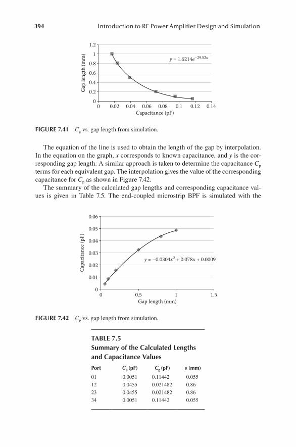
394 Introduction to RF Power Amplifier Design and Simulation
The equation of the line is used to obtain the length of the gap by interpolation. In the equation on the graph, x corresponds to known capacitance, and y is the cor-responding gap length. A similar approach is taken to determine the capacitance Cp terms for each equivalent gap. The interpolation gives the value of the corresponding capacitance for Cp as shown in Figure 7.42.
The summary of the calculated gap lengths and corresponding capacitance val-ues is given in Table 7.5. The end-coupled microstrip BPF is simulated with the
1.2
1
0.8
0.6
0.4
0.2
00 0.02 0.04 0.06 0.08
Capacitance (pF)
y = 1.6214e–29.52x
Gap
leng
th (m
m)
0.1 0.12 0.14
FIGURE 7.41 Cg vs. gap length from simulation.
0.06
0.05
0.04
0.03
0.02
0.01
00 0.5 1
Gap length (mm)
y = –0.0304x2 + 0.078x + 0.0009
Capa
cita
nce (
pF)
1.5
FIGURE 7.42 Cp vs. gap length from simulation.
TABLE 7.5Summary of the Calculated Lengths and Capacitance Values
Port Cp (pF) Cg (pF) s (mm)
01 0.0051 0.11442 0.055
12 0.0455 0.021482 0.86
23 0.0455 0.021482 0.86
34 0.0051 0.11442 0.055
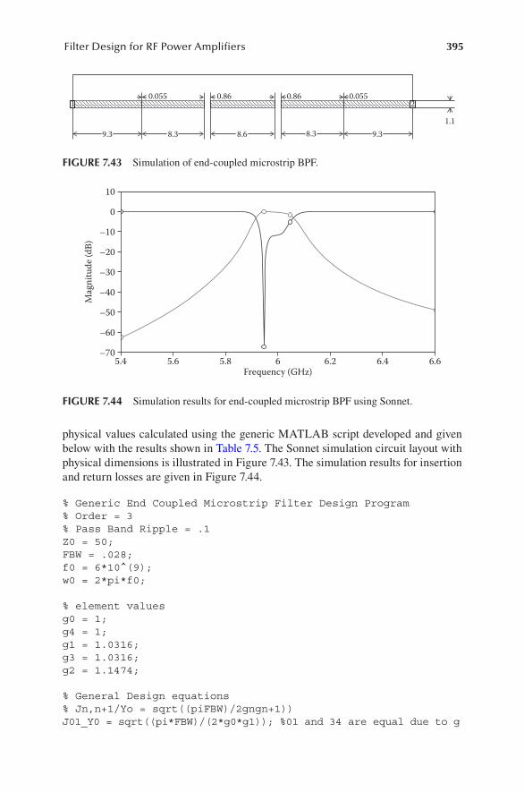
395Filter Design for RF Power Amplifiers
physical values calculated using the generic MATLAB script developed and given below with the results shown in Table 7.5. The Sonnet simulation circuit layout with physical dimensions is illustrated in Figure 7.43. The simulation results for insertion and return losses are given in Figure 7.44.
% Generic End Coupled Microstrip Filter Design Program % Order = 3% Pass Band Ripple = .1Z0 = 50;FBW = .028;f0 = 6*10^(9);w0 = 2*pi*f0;
% element valuesg0 = 1;g4 = 1;g1 = 1.0316;g3 = 1.0316;g2 = 1.1474;
% General Design equations% Jn,n+1/Yo = sqrt((piFBW)/2gngn+1))J01_Y0 = sqrt((pi*FBW)/(2*g0*g1)); %01 and 34 are equal due to g
21
9.31.1
8.38.68.3
0.055 0.86 0.86 0.055
9.3
FIGURE 7.43 Simulation of end-coupled microstrip BPF.
10
–10
–20
–30
–40
–50
–60
–705.4 5.6 5.8 6
Frequency (GHz)
Mag
nitu
de (d
B)
6.2 6.4 6.6
0
FIGURE 7.44 Simulation results for end-coupled microstrip BPF using Sonnet.
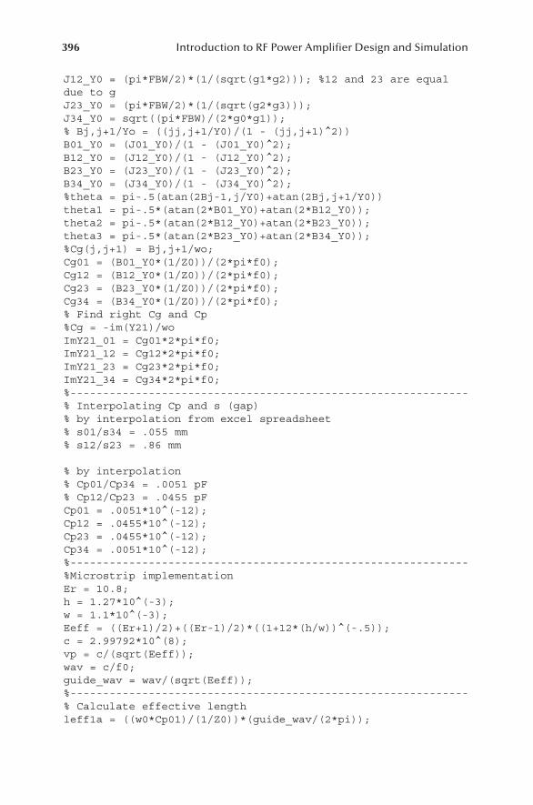
396 Introduction to RF Power Amplifier Design and Simulation
J12_Y0 = (pi*FBW/2)*(1/(sqrt(g1*g2))); %12 and 23 are equal due to gJ23_Y0 = (pi*FBW/2)*(1/(sqrt(g2*g3)));J34_Y0 = sqrt((pi*FBW)/(2*g0*g1));% Bj,j+1/Yo = ((jj,j+1/Y0)/(1 - (jj,j+1)^2))B01_Y0 = (J01_Y0)/(1 - (J01_Y0)^2);B12_Y0 = (J12_Y0)/(1 - (J12_Y0)^2);B23_Y0 = (J23_Y0)/(1 - (J23_Y0)^2);B34_Y0 = (J34_Y0)/(1 - (J34_Y0)^2);%theta = pi-.5(atan(2Bj-1,j/Y0)+atan(2Bj,j+1/Y0))theta1 = pi-.5*(atan(2*B01_Y0)+atan(2*B12_Y0));theta2 = pi-.5*(atan(2*B12_Y0)+atan(2*B23_Y0));theta3 = pi-.5*(atan(2*B23_Y0)+atan(2*B34_Y0));%Cg(j,j+1) = Bj,j+1/wo;Cg01 = (B01_Y0*(1/Z0))/(2*pi*f0);Cg12 = (B12_Y0*(1/Z0))/(2*pi*f0);Cg23 = (B23_Y0*(1/Z0))/(2*pi*f0);Cg34 = (B34_Y0*(1/Z0))/(2*pi*f0);% Find right Cg and Cp%Cg = -im(Y21)/woImY21_01 = Cg01*2*pi*f0;ImY21_12 = Cg12*2*pi*f0;ImY21_23 = Cg23*2*pi*f0;ImY21_34 = Cg34*2*pi*f0;%-------------------------------------------------------------% Interpolating Cp and s (gap)% by interpolation from excel spreadsheet% s01/s34 = .055 mm% s12/s23 = .86 mm
% by interpolation% Cp01/Cp34 = .0051 pF% Cp12/Cp23 = .0455 pFCp01 = .0051*10^(-12);Cp12 = .0455*10^(-12);Cp23 = .0455*10^(-12);Cp34 = .0051*10^(-12);%-------------------------------------------------------------%Microstrip implementationEr = 10.8;h = 1.27*10^(-3);w = 1.1*10^(-3);Eeff = ((Er+1)/2)+((Er-1)/2)*((1+12*(h/w))^(-.5));c = 2.99792*10^(8);vp = c/(sqrt(Eeff));wav = c/f0;guide_wav = wav/(sqrt(Eeff));%-------------------------------------------------------------% Calculate effective lengthleff1a = ((w0*Cp01)/(1/Z0))*(guide_wav/(2*pi));
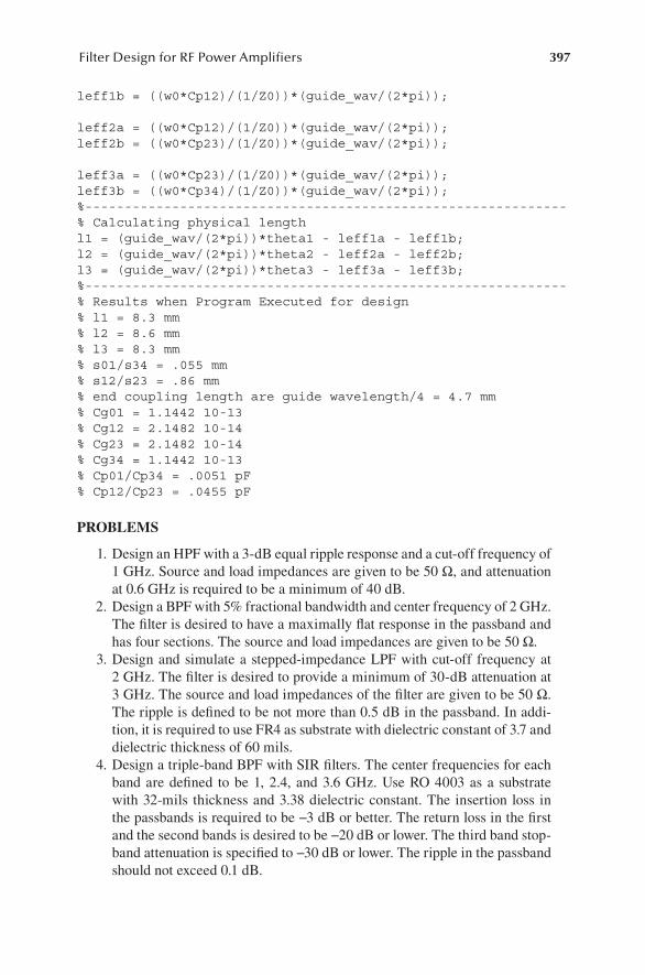
397Filter Design for RF Power Amplifiers
leff1b = ((w0*Cp12)/(1/Z0))*(guide_wav/(2*pi));
leff2a = ((w0*Cp12)/(1/Z0))*(guide_wav/(2*pi));leff2b = ((w0*Cp23)/(1/Z0))*(guide_wav/(2*pi));
leff3a = ((w0*Cp23)/(1/Z0))*(guide_wav/(2*pi));leff3b = ((w0*Cp34)/(1/Z0))*(guide_wav/(2*pi));%-------------------------------------------------------------% Calculating physical lengthl1 = (guide_wav/(2*pi))*theta1 - leff1a - leff1b; l2 = (guide_wav/(2*pi))*theta2 - leff2a - leff2b;l3 = (guide_wav/(2*pi))*theta3 - leff3a - leff3b; %-------------------------------------------------------------% Results when Program Executed for design% l1 = 8.3 mm% l2 = 8.6 mm% l3 = 8.3 mm% s01/s34 = .055 mm% s12/s23 = .86 mm% end coupling length are guide wavelength/4 = 4.7 mm% Cg01 = 1.1442 10-13% Cg12 = 2.1482 10-14% Cg23 = 2.1482 10-14% Cg34 = 1.1442 10-13% Cp01/Cp34 = .0051 pF% Cp12/Cp23 = .0455 pF
PROBLEMS
1. Design an HPF with a 3-dB equal ripple response and a cut-off frequency of 1 GHz. Source and load impedances are given to be 50 Ω, and attenuation at 0.6 GHz is required to be a minimum of 40 dB.
2. Design a BPF with 5% fractional bandwidth and center frequency of 2 GHz. The filter is desired to have a maximally flat response in the passband and has four sections. The source and load impedances are given to be 50 Ω.
3. Design and simulate a stepped-impedance LPF with cut-off frequency at 2 GHz. The filter is desired to provide a minimum of 30-dB attenuation at 3 GHz. The source and load impedances of the filter are given to be 50 Ω. The ripple is defined to be not more than 0.5 dB in the passband. In addi-tion, it is required to use FR4 as substrate with dielectric constant of 3.7 and dielectric thickness of 60 mils.
4. Design a triple-band BPF with SIR filters. The center frequencies for each band are defined to be 1, 2.4, and 3.6 GHz. Use RO 4003 as a substrate with 32-mils thickness and 3.38 dielectric constant. The insertion loss in the passbands is required to be −3 dB or better. The return loss in the first and the second bands is desired to be −20 dB or lower. The third band stop-band attenuation is specified to −30 dB or lower. The ripple in the passband should not exceed 0.1 dB.

398 Introduction to RF Power Amplifier Design and Simulation
REFERENCES
1. A. Eroglu. 2013. RF Circuit Design Techniques for MF-UHF Applications. CRC Press, Boca Raton, FL.
2. A. Eroglu, and J.K. Lee. 2008. The complete design of microstrip directional couplers using the synthesis technique. IEEE Transactions on Microwave Theory and Techniques, Vol. 57, No. 12, pp. 2756–2761, December.
399
8 Computer Aided Design Tools for Amplifier Design and Implementation
8.1 INTRODUCTION
Radio frequency (RF)/microwave computer-aided design (CAD) tools have been com-monly used in RF power amplifier systems to expedite the design process, increase the system performance, and reduce the associated cost by eliminating the need for several prototypes before the implementation stage [1–3]. RF power amplifiers are simulated with nonlinear circuit simulators, which use large signal equivalent mod-els of the active devices. Passive components used in RF power amplifier simulation are usually modeled as ideal components and hence do not include the frequency characteristics. Furthermore, it is rare to include the electromagnetic effects such as coupling between traces and leads, parasitic effects, current distribution, and radia-tion effects that exist among the components in RF power amplifier simulation. This is partly due to the requirement in expertise in both nonlinear circuit simulators and electromagnetic simulators.
Nonlinear circuit simulation of RF power amplifiers can be done using harmonic balance technique with the application of Krylov subspace methods in the frequency domain or nonlinear differential algebraic equations using the integration methods, Newton’s method, or sparse matrix solution techniques in the time domain [4–6]. Time-domain methods are preferred over frequency-domain methods because of their advantage in providing accurate solutions using the transient response of the circuits.
RF amplifier design therefore can be systematized from the component level to the assembly level and from the assembly level to the system level using CAD tools with the implementation of the design flow diagram given in Figure 8.1. RF ampli-fier design methodology given in Figure 8.1 consists of three phases: analysis phase, simulation phase, and experimental phase. As seen in the flow diagram, the simula-tion stage is the bridge to the experimental stage and is required for an optimized successful design.
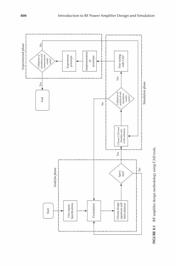
400 Introduction to RF Power Amplifier Design and Simulation
Ana
lysis
pha
se
Star
t
Use
r inp
uts
Spec
ifica
tions
Form
ulat
ion
Choo
se d
esig
neq
uatio
ns an
dfin
d so
lutio
ns
Spec
sm
et?
Choo
se C
AD
tool
Sim
ulat
e and
verif
y sol
utio
ns
Yes
No
Valid
atio
n of
anal
ytic
al an
dsim
ulat
ion
resu
ltssa
me?
No
Yes
Fine
-tuni
ngw
ith C
AD
Valid
atio
n of
simul
atio
n an
dm
easu
rem
ent
resu
ltssa
me?
Expe
rimen
tpr
otot
ype
No
End
Yes
Impl
emen
tatio
nof
prot
otyp
e
Sim
ulat
ion
phas
e
Expe
rimen
tal p
hase
FIG
UR
E 8.
1 R
F am
plifi
er d
esig
n m
etho
dolo
gy u
sing
CA
D to
ols.
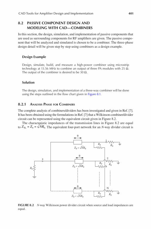
401CAD Tools for Amplifier Design and Implementation
8.2 PASSIVE COMPONENT DESIGN AND MODELING WITH CAD—COMBINERS
In this section, the design, simulation, and implementation of passive components that are used as surrounding components for RF amplifiers are given. The passive compo-nent that will be analyzed and simulated is chosen to be a combiner. The three-phase design detail will be given step by step using combiners as a design example.
Design Example
Design, simulate, build, and measure a high-power combiner using microstrip technology at 13.56 MHz to combine an output of three PA modules with 25 Ω. The output of the combiner is desired to be 30 Ω.
Solution
The design, simulation, and implementation of a three-way combiner will be done using the steps outlined in the flow chart given in Figure 8.1.
8.2.1 AnAlysis PhAse for Combiners
The complete analysis of combiners/dividers has been investigated and given in Ref. [7]. It has been obtained using the formulations in Ref. [7] that a Wilkinson combiner/divider circuit can be represented using the equivalent circuit given in Figure 8.2.
The characteristic impedances of the transmission lines in Figure 8.2 are equal to Z Z NRTL 0 0= = . The equivalent four-port network for an N-way divider circuit is
Z0 = NR0
Z0 = NR0
Z0 = NR0
R0
a
b
1
2
N
R0
R0 R0
R0
R0R0
θ
θ
θ
FIGURE 8.2 N-way Wilkinson power divider circuit when source and load impedances are equal.
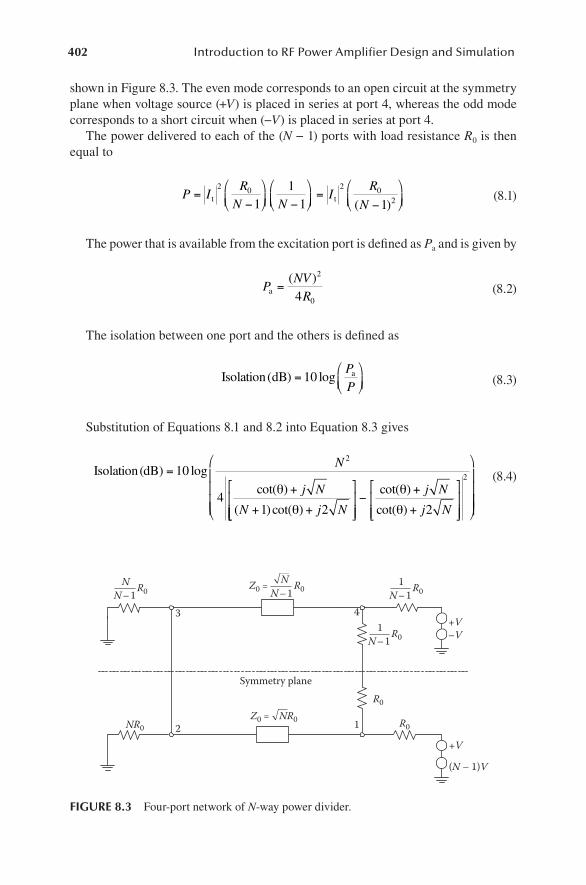
402 Introduction to RF Power Amplifier Design and Simulation
shown in Figure 8.3. The even mode corresponds to an open circuit at the symmetry plane when voltage source (+V) is placed in series at port 4, whereas the odd mode corresponds to a short circuit when (−V) is placed in series at port 4.
The power delivered to each of the (N − 1) ports with load resistance R0 is then equal to
P IRN N
IR
N=
−
−
=
−
t t
2 2
2111 1
0 0
( ) (8.1)
The power that is available from the excitation port is defined as Pa and is given by
PNVRa0
=( )2
4 (8.2)
The isolation between one port and the others is defined as
Isolation dB a( ) log= 10PP (8.3)
Substitution of Equations 8.1 and 8.2 into Equation 8.3 gives
Isolation(dB) =+
+ +
10
41 2
2
logcot( )
( )cot( )
N
j N
N j N
θ
θ
−
+
+
cot( )
cot( )
θ
θ
j N
j N2
2
(8.4)
3
N R0N – 1
1
Symmetry plane
2
4
N R0
+V
+V–V
(N – 1)V
NR0
R0
R0
1 R0N – 1N – 1
1 R0N – 1
Z0 = NR0
Z0 =
FIGURE 8.3 Four-port network of N-way power divider.
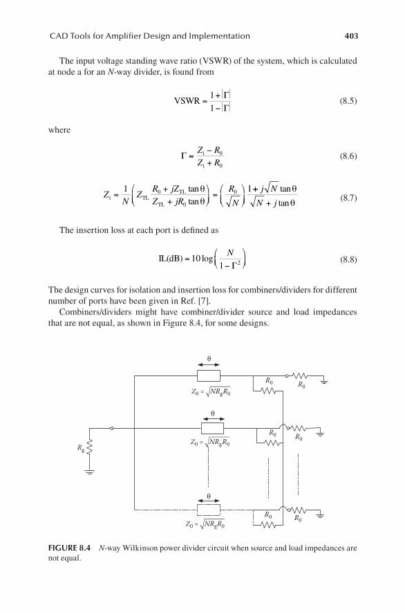
403CAD Tools for Amplifier Design and Implementation
The input voltage standing wave ratio (VSWR) of the system, which is calculated at node a for an N-way divider, is found from
VSWR =+
−
1
1
Γ
Γ (8.5)
where
Γ =−+
Z RZ Ri 0
i 0
(8.6)
ZN
ZR jZZ jR
R
Ni TL
TL
TL
=++
=
1 10
0
0tantan
θθ
++
+
j N
N j
tan
tan
θ
θ (8.7)
The insertion loss at each port is defined as
IL(dB) log=−
101 2
N
Γ (8.8)
The design curves for isolation and insertion loss for combiners/dividers for different number of ports have been given in Ref. [7].
Combiners/dividers might have combiner/divider source and load impedances that are not equal, as shown in Figure 8.4, for some designs.
Rg
R0 R0
R0
R0R0
R0
θ
θ
θ
Z0 = NRgR0
Z0 = NRgR0
Z0 = NRgR0
FIGURE 8.4 N-way Wilkinson power divider circuit when source and load impedances are not equal.
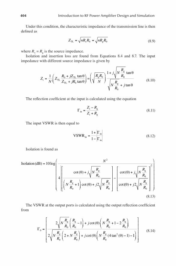
404 Introduction to RF Power Amplifier Design and Simulation
Under this condition, the characteristic impedance of the transmission line is then defined as
Z nR R nR RTL x g= =0 0 (8.9)
where Rx = Rg is the source impedance.Isolation and insertion loss are found from Equations 8.4 and 8.7. The input
impedance with different source impedance is given by
ZN
ZR jZZ jR
R R
Ni TLTL
TL
g==++
1 0
0
0tantan
θθ
+
+
10
0
j NR
R
NR
Rj
g
g
tan
tan
θ
θ (8.10)
The reflection coefficient at the input is calculated using the equation
Γ ini g
i g
=−
+
Z R
Z R (8.11)
The input VSWR is then equal to
VSWRinin
in
=+
−
1
1
Γ
Γ (8.12)
Isolation is found as
Isolation(dB)
g
g
=
+
+
10
4
1
2
0
0
log
cot ( )
N
j NR
R
NR
R
θ
+
−
+
cot ( )
cot ( )
cotθ
θ
j NR
R
j NR
R
20
0
g
g
(( )θ +
j NR
R2
0
2
g
(8.13)
The VSWR at the output ports is calculated using the output reflection coefficient from
Γ00 0 0 0
2 1 1 2
=
−
+ + −
NR
R
R
Rj N
R
R
R
Rg g g gcot ( )θ
+
+ − −2 2 4 1
0 0 0
2NR
RNR
Rj N
R
Rg g gcot ( ) ( tan ( ) )θ θ 11
(8.14)
405CAD Tools for Amplifier Design and Implementation
Then, output VSWR is found by
VSWRoutout
out
=+
−
1
1
Γ
Γ (8.15)
The distributed elements can be transformed to the lumped elements for frequen-cies less than 100 MHz using the for a quarter-wavelength-long transmission line as shown in Figure 8.5.
In Figure 8.5, the element values for the lumped components can be found using the following formulas:
L
Zf
CfZ
= =0
021
2π π, (8.16)
The network in Figure 8.5 also performs impedance transformation from R1 to R2 at each distribution port on the combiner. The lumped-element transformation network shown is a π-network, and it consists of three reactive elements. The quality factor for this network can be found from
Q = R1/Xc (8.17)
The number of reactive elements can be reduced by transforming the π-network to the L-network, as shown in Figure 8.6. Q of the π-network can be used to obtain the corresponding element values for the L-network when it is transformed. The equivalent L-network is given in Figure 8.6 when R1 ≥ R2.
As a result, each distributed element in Figures 8.2 and 8.4 can be replaced with its equivalent lumped-element L-network shown in Figure 8.6b.
C C
Lλ/4 R1 R2R2R1
FIGURE 8.5 Distributed element to lumped conversion.
(a)
C2 C3 C4
R1 R2L1 L2R2 R1
(b)
FIGURE 8.6 Transformation from (a) π-network to (b) L-network.
406 Introduction to RF Power Amplifier Design and Simulation
For the design example given, the operational frequency is 13.56 MHz, and the combiner should be capable of providing 12,000-W output power. The combiner is intended to combine the outputs of three PA modules. Each PA module presents 25-Ω impedance to the input of each distribution port on the combiner. The output of the combiner is desired to be 30-Ω. MATLAB GUI in Ref. [7] is used for the com-biner to obtain insertion loss, isolation, VSWRs, and characteristic curves, as shown in Figure 8.7. The program does not take into account any imperfection that might exist in the real system and hence theoretically gives perfect isolation when θ = 90°. The design parameters for the three-way combiner are
R0 = 25 Ω, RL = 30 Ω, Z0 = 47.43 Ω (8.18)
Each PA module is required to provide 4000-W output power under a matched con-dition. The component values calculated using Equation 8.14 for the π-network given in Figure 8.6a are
L1 = 556.69 nH, C2 = C3 = 247.46 pF, Q = 1.898 (8.19)
The corresponding component values of the lumped elements for the L-network given in Figure 8.6b are
L3 = 472.2 nH, C4 = 210.5 pF, Q = 1.612 (8.20)
In both circuits,
R1 = 90 Ω, and R2 = 25 Ω (8.21)
FIGURE 8.7 MATLAB GUI output for three-way unbalanced combiner when θ = 90°.
407CAD Tools for Amplifier Design and Implementation
The lumped-element inductor in the L-network is implemented as a spiral induc-tor on an alumina substrate having a planar form. The form of the spiral inductor that will be used in our application is shown in Figure 8.8. It is a rectangular spiral induc-tor with rounded edges versus sharp edges. This type of implementation on the edges increases the effective arcing distance between traces. The physical dimensions for the spiral inductor are the width of the trace, w, the length of the outside edges, l1 and l2, and the spacing between the traces, s. The simplified two-port, lumped-element equivalent circuit for the spiral inductor shown in Figure 8.8 is illustrated in Figure 8.9. In Figure 8.9, L is the series inductance of the spiral, and C is the substrate capacitance.
This model ignores the losses in the substrate and the conductor. The lumped-element values for the spiral inductor to perform the required impedance transfor-mation from R2 = 25 Ω to R1 = 90 Ω for the network in Figure 8.9 are calculated to be
L = 497 nH, C = 43.6 pF
The accurate inductance calculation at the high-frequency range can be obtained using Greenhouse’s method described in Ref. [8]. The total inductance of the spiral inductor including the effect of mutual couplings is given as
L = L0 + ∑M (8.22)
L0 is the sum of the self inductances for each trace. ∑M takes into account all the mutual inductances in the structure. Equation 8.22 can be written more explicitly for any number of turns for a rectangular spiral inductor as
L ll
lTi i
i
iGMDAMD
=
− + +
0 0002 2 1 25
4. ln .
µ (8.23)
w
s
l2
l1
FIGURE 8.8 Spiral inductor model.
408 Introduction to RF Power Amplifier Design and Simulation
and
Mij = 0.0002liQi (8.24)
AMD is the arithmetic mean distance, and GMD is used for the geometric dis-tance. C is the capacitance that includes the effect of odd mode, even mode, and interline coupling capacitances between coupled lines of the spiral inductor. The detailed calculation of the capacitances is given in Ref. [9]. The substrate losses and conductor losses are ignored due to the low operational frequency.
The one-port measurement network for the spiral inductor using the model pro-posed in Figure 8.9 is shown in Figure 8.10. When the equivalent one-port measure-ment network is used, the effective inductance value is found using Z = jωLeff
Leff = 589.2 nH from Z = jωLeff (8.25)
The physical dimensions of the microstrip spiral inductor are calculated using the formulation and algorithm developed in Ref. [10] and are given in Table 8.1.
At this point, all the formulation has been done, and solutions are obtained. Based on the analytical values, the combiner meets the specifications. Hence, we are ready at this point to perform the second phase of the design stage.
8.2.2 simulAtion PhAse for Combiners
The spiral inductor using the dimensions in Table 8.1 is simulated with the method of the moment-based planar electromagnetic simulator, Sonnet. The operational frequency is chosen to be 13.56 MHz. The 3D layout of the simulated structure is illustrated in Figure 8.11. The input port or port 1 is connected via the bridge for inductance mea-surement. The bridge height and width are given in Table 8.1. The effect of the bridge at the frequency of the operation is minimal due to its increased width.
C C
L P2P1
FIGURE 8.9 Simplified equivalent circuit for spiral inductor without loss factor.
LC
P1
P2
Z, fop
FIGURE 8.10 One-port measurement circuit.
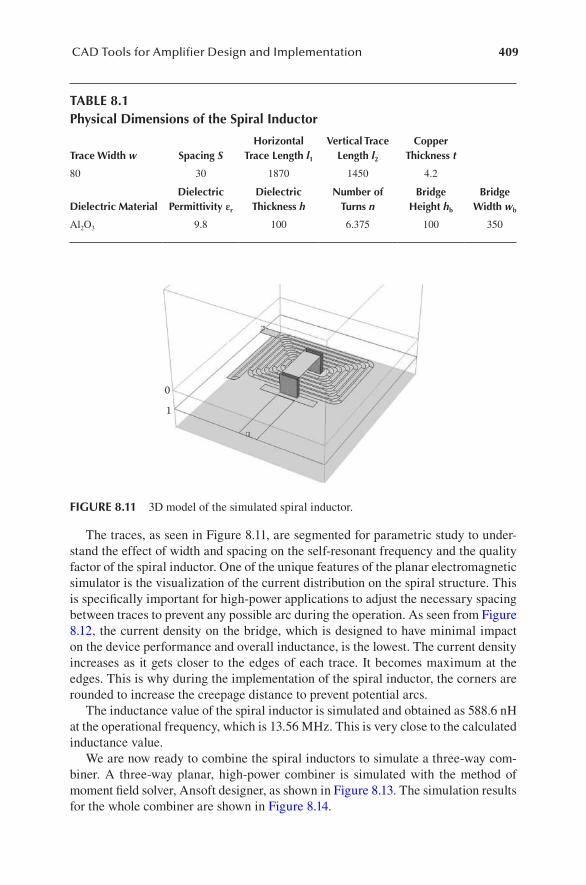
409CAD Tools for Amplifier Design and Implementation
The traces, as seen in Figure 8.11, are segmented for parametric study to under-stand the effect of width and spacing on the self-resonant frequency and the quality factor of the spiral inductor. One of the unique features of the planar electromagnetic simulator is the visualization of the current distribution on the spiral structure. This is specifically important for high-power applications to adjust the necessary spacing between traces to prevent any possible arc during the operation. As seen from Figure 8.12, the current density on the bridge, which is designed to have minimal impact on the device performance and overall inductance, is the lowest. The current density increases as it gets closer to the edges of each trace. It becomes maximum at the edges. This is why during the implementation of the spiral inductor, the corners are rounded to increase the creepage distance to prevent potential arcs.
The inductance value of the spiral inductor is simulated and obtained as 588.6 nH at the operational frequency, which is 13.56 MHz. This is very close to the calculated inductance value.
We are now ready to combine the spiral inductors to simulate a three-way com-biner. A three-way planar, high-power combiner is simulated with the method of moment field solver, Ansoft designer, as shown in Figure 8.13. The simulation results for the whole combiner are shown in Figure 8.14.
0
1
1
2
FIGURE 8.11 3D model of the simulated spiral inductor.
TABLE 8.1Physical Dimensions of the Spiral Inductor
Trace Width w Spacing SHorizontal
Trace Length l1
Vertical Trace Length l2
Copper Thickness t
80 30 1870 1450 4.2
Dielectric MaterialDielectric
Permittivity εr
Dielectric Thickness h
Number of Turns n
Bridge Height hb
Bridge Width wb
Al2O3 9.8 100 6.375 100 350
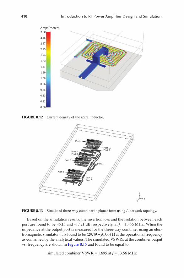
410 Introduction to RF Power Amplifier Design and Simulation
Based on the simulation results, the insertion loss and the isolation between each port are found to be –5.15 and –17.21 dB, respectively, at f = 13.56 MHz. When the impedance at the output port is measured for the three-way combiner using an elec-tromagnetic simulator, it is found to be (29.49 − j0.06) Ω at the operational frequency as confirmed by the analytical values. The simulated VSWRs at the combiner output vs. frequency are shown in Figure 8.15 and found to be equal to
simulated combiner VSWR = 1.695 at f = 13.56 MHz
Port 1
Port 10Port 9Port 7
Port 8
Port 3
Port 2
Port 6Port 5
Port 1
Z
YX
FIGURE 8.13 Simulated three-way combiner in planar form using L-network topology.
2.80Amps/meters
2.58
2.37
2.15
1.94
1.72
1.51
1.29
1.08
0.86
0.65
0.43
0.22
0.00
2
1
FIGURE 8.12 Current density of the spiral inductor.
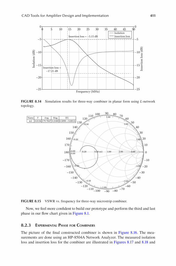
411CAD Tools for Amplifier Design and Implementation
Now, we feel more confident to build our prototype and perform the third and last phase in our flow chart given in Figure 8.1.
8.2.3 exPerimentAl PhAse for Combiners
The picture of the final constructed combiner is shown in Figure 8.16. The mea-surements are done using an HP-8504A Network Analyzer. The measured isolation loss and insertion loss for the combiner are illustrated in Figures 8.17 and 8.18 and
0
–5
–10
–15
–20
Frequency (MHz)
Isol
atio
n (d
B)
Inse
rtio
n lo
ss (d
B)
–25
00 5 10 15 20 25 30 35 40 45 50
–5
–10
–15
–20
–25
Insertion loss = –5.15 dB
Insertion loss =–17.21 dB
IsolationInsertion loss
FIGURE 8.14 Simulation results for three-way combiner in planar form using L-network topology.
90 80 7060
5040
30
20
10
0
–10
–20
–30–40
–50–60
–70–80
100110120
130 0.50
1.00
2.00
5.000.20
0.000.00
–0.20
–0.50
–1.00
–2.00
–5.00
5.002.001.000.50 m10.20
140150
160
170
180
–170
–160
–150–140
–130–120
–110–100 –90
Namem1
F0.0136
Ang179.7847
Mag0.2580
RX0.5898 + 0.0012i
FIGURE 8.15 VSWR vs. frequency for three-way microstrip combiner.
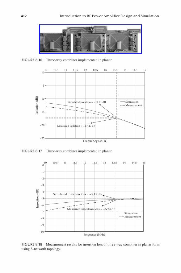
412 Introduction to RF Power Amplifier Design and Simulation
FIGURE 8.16 Three-way combiner implemented in planar.
1010
–5
–10
–15
–20
–25
10.5 11 11.5 12 12.5
Frequency (MHz)
Measured isolation = –17.47 dB
Simulated isolation = –17.21 dB
Isol
atio
n (d
B)
13 13.5 14 14.5 15
SimulationMeasurement
FIGURE 8.17 Three-way combiner implemented in planar.
Frequency (MHz)
Simulated insertion loss = –5.15 dB
SimulationMeasurement
10 10.5 11 11.5 12 12.5 13 13.5 14 14.5 150
–2
–3
–1
–4
–5
–8
–7
–6
–10
–9
Inse
rtio
n (d
B)
Measured insertion loss = –5.24 dB
FIGURE 8.18 Measurement results for insertion loss of three-way combiner in planar form using L-network topology.

413CAD Tools for Amplifier Design and Implementation
compared with the simulated results. The isolation loss and insertion loss at the operational frequency are measured to be –17.47 and –5.24 dB, respectively.
The impedance at the output port under this condition is measured to be (30.23 − j0.06) Ω at the operational frequency. This corresponds to
measured combiner VSWR = 1.654 at f = 13.56 MHz
This value is very close to the targeted impedance value of 30 Ω at the output port.The measured insertion loss and return loss are given in Figures 8.17 and 8.18,
respectively, with comparison with the simulated results. As seen, the simulated and analytical results are in agreement, and design methodology introduced by the flow chart given in Figure 8.1 leads to completion and realization of a successful design.
8.3 ACTIVE COMPONENT DESIGN AND MODELING WITH CAD
It is a requirement for active devices to be able to handle high power, high gain, and stability for some RF/microwave applications including semiconductor wafer processing and medical resonance imaging. Active devices also have to be rugged, withstand high voltage swing, and have good thermal profile when used as a compo-nent in RF amplifiers.
There has been extensive study on failure modes of semiconductor devices to iden-tify the root causes of wire-bond failures and bonding pad fatigue [11]. The investigation of the failure mechanisms of high-power devices led to the inclusion of other sources of failure such as die-attach voids and degradation of the bonding pad. The recent advance-ment in technology helped to relate some of the wire-bond failures to hotspots created by voids under the silicon die. This initiated research into the growth of these die-attach layer cracks to improve the reliability of active devices that are used in RF/microwave amplifiers. As a result, the design and manufacturing of a die with the desired package that will be used as an active device in RF systems need to have several design standards and the required electrical and mechanical properties to perform without failure.
Hence, it is necessary to have a novel package design for active devices to enable them to perform without failure. In this section, the flow chart in Figure 8.1 will be used to design, simulate, and build a hybrid package for a metal–oxide–semiconductor field-effect transistor (MOSFET). The three-phase design detail will be given step by step using the hybrid MOSFET package design.
Design Example
Design a hybrid package, and obtain package parasitics consisting of four dies to be used in power amplifiers operating at 13.56 MHz as a component to provide the required gain, power output, stability, and thermal profile.
Solution
The design, simulation, and implementation of hybrid package will be done using the steps outlined in the flow chart given in Figure 8.1.
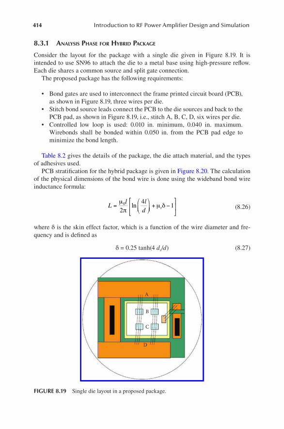
414 Introduction to RF Power Amplifier Design and Simulation
8.3.1 AnAlysis PhAse for hybrid PACkAge
Consider the layout for the package with a single die given in Figure 8.19. It is intended to use SN96 to attach the die to a metal base using high-pressure reflow. Each die shares a common source and split gate connection.
The proposed package has the following requirements:
• Bond gates are used to interconnect the frame printed circuit board (PCB), as shown in Figure 8.19, three wires per die.
• Stitch bond source leads connect the PCB to the die sources and back to the PCB pad, as shown in Figure 8.19, i.e., stitch A, B, C, D, six wires per die.
• Controlled low loop is used: 0.010 in. minimum, 0.040 in. maximum. Wirebonds shall be bonded within 0.050 in. from the PCB pad edge to minimize the bond length.
Table 8.2 gives the details of the package, the die attach material, and the types of adhesives used.
PCB stratification for the hybrid package is given in Figure 8.20. The calculation of the physical dimensions of the bond wire is done using the wideband bond wire inductance formula:
Ll l
d=
+ −
µπ
µ δ0
24
1ln r (8.26)
where δ is the skin effect factor, which is a function of the wire diameter and fre-quency and is defined as
δ = 0.25 tanh(4 ds/d) (8.27)
A
B
C
D
FIGURE 8.19 Single die layout in a proposed package.

415CAD Tools for Amplifier Design and Implementation
where ds is defined as
dfs
r
=ρ
π µ µ0 (8.28)
ρ is the resistivity of the bond wire, l is the length, and d is the diameter of the wire. Using Equations 8.26 through 8.28, we find the bond wire inductance as
Ll l
d=
+ −
=
µπ
µ δ0
24
1 3 65ln . [ ]r nH (8.29)
The physical length of the bond wire is usually very short, and therefore, the associated resistance is low. The DC resistance of the bond wire is calculated from
Rl
rdc =
ρ
π 2 (8.30)
For d/ds > 3.4 using curve fitting, we obtain
R Rdds dcs
= +0 25 0 2654. . (8.31)
The four dies when placed symmetrically in the final proposed package are illus-trated in Figure 8.21.
TABLE 8.2Details of the Proposed Package
Package Technology Die Attach Material Type
Pressed alumina ceramic Silver-filled glass Inorganic adhesive
Laminated alumina ceramic (pin grid array [PGA], ceramic quad flat pack [CQFP], side-braze)
Gold–silicon eutecticSilver-filled cyanate ester
Hard solderOrganic adhesive
Molded plastic Silver-filled epoxy Organic adhesive
ickness = 0.032 in.Material = Roger 4003
2 oz. Cu, all layers
FIGURE 8.20 PCB stratification.
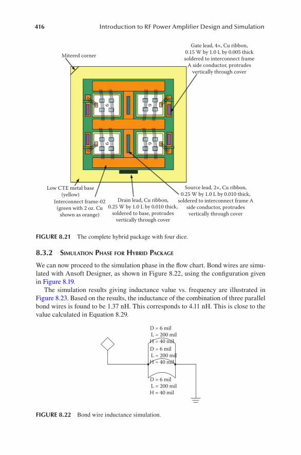
416 Introduction to RF Power Amplifier Design and Simulation
8.3.2 simulAtion PhAse for hybrid PACkAge
We can now proceed to the simulation phase in the flow chart. Bond wires are simu-lated with Ansoft Designer, as shown in Figure 8.22, using the configuration given in Figure 8.19.
The simulation results giving inductance value vs. frequency are illustrated in Figure 8.23. Based on the results, the inductance of the combination of three parallel bond wires is found to be 1.37 nH. This corresponds to 4.11 nH. This is close to the value calculated in Equation 8.29.
Mitered corner
Gate lead, 4×, Cu ribbon,0.15 W by 1.0 L by 0.005 thicksoldered to interconnect frame
A side conductor, protrudesvertically through cover
Low CTE metal base(yellow)
Interconnect frame-02(green with 2 oz. Cu
shown as orange)
Drain lead, Cu ribbon,0.25 W by 1.0 L by 0.010 thick,
soldered to base, protrudesvertically through cover
Source lead, 2×, Cu ribbon,0.25 W by 1.0 L by 0.010 thick,
soldered to interconnect frame Aside conductor, protrudesvertically through cover
6 9
6 9
FIGURE 8.21 The complete hybrid package with four dice.
D = 6 milL = 200 milH = 40 mil
D = 6 milL = 200 milH = 40 mil
D = 6 milL = 200 milH = 40 mil
FIGURE 8.22 Bond wire inductance simulation.
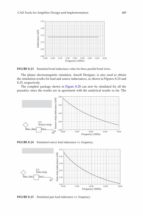
417CAD Tools for Amplifier Design and Implementation
The planar electromagnetic simulator, Ansoft Designer, is also used to obtain the simulation results for lead and source inductances, as shown in Figures 8.24 and 8.25, respectively.
The complete package shown in Figure 8.20 can now be simulated for all the parasitics since the results are in agreement with the analytical results so far. The
1.25
1.20
1.15
1.10
1.05
1.0012.80 13.00 13.20 13.40 13.60
Frequency (MHz)
Indu
ctan
ce (n
H)
13.80 14.00 14.20 14.40
FIGURE 8.23 Simulated bond inductance value for three parallel bond wires.
2.84
2.83
2.83
2.82
2.8210.00 15.00 20.00
Frequency (MHz)
Sour
ce st
rip in
duct
ance
(nH
)
25.00 30.000
U1Source strip
Port 2Port 1Port 1
FIGURE 8.24 Simulated source lead inductance vs. frequency.
4.37
4.36
4.36
4.35
4.35
4.3410.00 15.00 20.00
Frequency (MHz)
Gat
e str
ip in
duct
ance
(nH
)
25.00 30.00
U1Gate strip
Port 2Port 1Port 10
FIGURE 8.25 Simulated gate lead inductance vs. frequency.
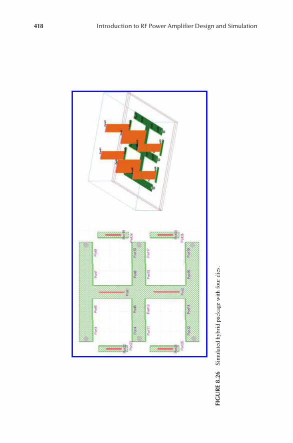
418 Introduction to RF Power Amplifier Design and Simulation
FIG
UR
E 8.
26
Sim
ulat
ed h
ybri
d pa
ckag
e w
ith
four
die
s.
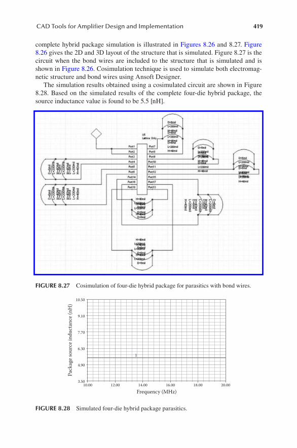
419CAD Tools for Amplifier Design and Implementation
complete hybrid package simulation is illustrated in Figures 8.26 and 8.27. Figure 8.26 gives the 2D and 3D layout of the structure that is simulated. Figure 8.27 is the circuit when the bond wires are included to the structure that is simulated and is shown in Figure 8.26. Cosimulation technique is used to simulate both electromag-netic structure and bond wires using Ansoft Designer.
The simulation results obtained using a cosimulated circuit are shown in Figure 8.28. Based on the simulated results of the complete four-die hybrid package, the source inductance value is found to be 5.5 [nH].
FIGURE 8.27 Cosimulation of four-die hybrid package for parasitics with bond wires.
1
10.50
9.10
7.70
6.30
4.90
3.5010.00 12.00 14.00 16.00
Frequency (MHz)
Pack
age s
ourc
e ind
ucta
nce (
nH)
18.00 20.00
FIGURE 8.28 Simulated four-die hybrid package parasitics.
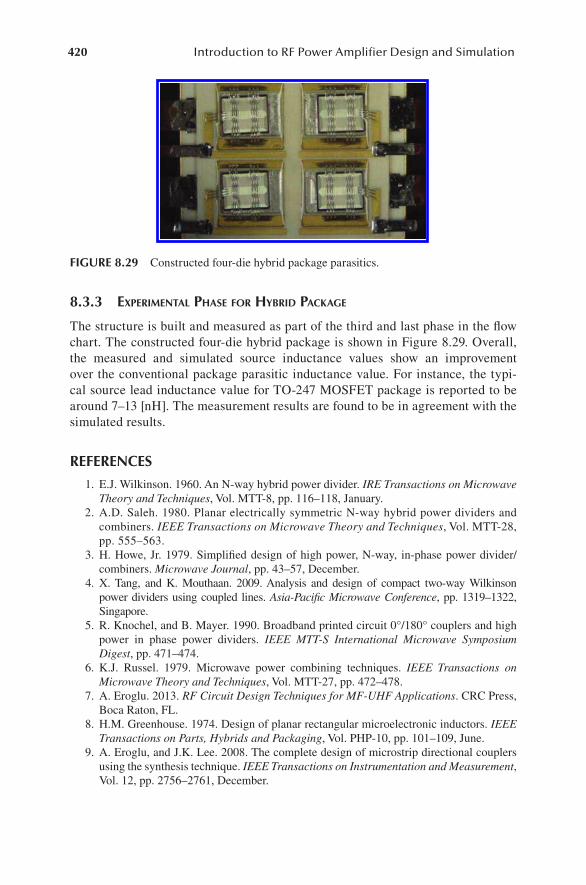
420 Introduction to RF Power Amplifier Design and Simulation
8.3.3 exPerimentAl PhAse for hybrid PACkAge
The structure is built and measured as part of the third and last phase in the flow chart. The constructed four-die hybrid package is shown in Figure 8.29. Overall, the measured and simulated source inductance values show an improvement over the conventional package parasitic inductance value. For instance, the typi-cal source lead inductance value for TO-247 MOSFET package is reported to be around 7–13 [nH]. The measurement results are found to be in agreement with the simulated results.
REFERENCES
1. E.J. Wilkinson. 1960. An N-way hybrid power divider. IRE Transactions on Microwave Theory and Techniques, Vol. MTT-8, pp. 116–118, January.
2. A.D. Saleh. 1980. Planar electrically symmetric N-way hybrid power dividers and combiners. IEEE Transactions on Microwave Theory and Techniques, Vol. MTT-28, pp. 555–563.
3. H. Howe, Jr. 1979. Simplified design of high power, N-way, in-phase power divider/combiners. Microwave Journal, pp. 43–57, December.
4. X. Tang, and K. Mouthaan. 2009. Analysis and design of compact two-way Wilkinson power dividers using coupled lines. Asia-Pacific Microwave Conference, pp. 1319–1322, Singapore.
5. R. Knochel, and B. Mayer. 1990. Broadband printed circuit 0°/180° couplers and high power in phase power dividers. IEEE MTT-S International Microwave Symposium Digest, pp. 471–474.
6. K.J. Russel. 1979. Microwave power combining techniques. IEEE Transactions on Microwave Theory and Techniques, Vol. MTT-27, pp. 472–478.
7. A. Eroglu. 2013. RF Circuit Design Techniques for MF-UHF Applications. CRC Press, Boca Raton, FL.
8. H.M. Greenhouse. 1974. Design of planar rectangular microelectronic inductors. IEEE Transactions on Parts, Hybrids and Packaging, Vol. PHP-10, pp. 101–109, June.
9. A. Eroglu, and J.K. Lee. 2008. The complete design of microstrip directional couplers using the synthesis technique. IEEE Transactions on Instrumentation and Measurement, Vol. 12, pp. 2756–2761, December.
FIGURE 8.29 Constructed four-die hybrid package parasitics.

421CAD Tools for Amplifier Design and Implementation
10. A. Eroglu. 2011. Planar inductor design for high power applications. Progress in Electromagnetic Research B, Vol. 35, pp. 53–67, December.
11. A. Hamidi, N. Beck, K. Thomas, and E. Herr. 1999. Effects of current density and chip temperature distribution on lifetime of high power IGBT modules in traction work-ing conditions. Microelectronics & Reliability, Vol. 39, Nos. 6–7, pp. 1153–1158, June–July.

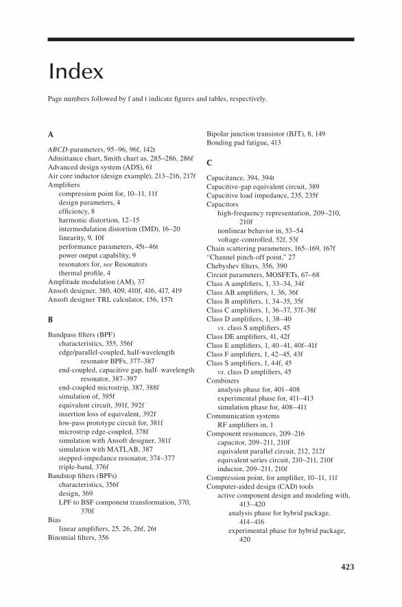
423
IndexPage numbers followed by f and t indicate figures and tables, respectively.
A
ABCD-parameters, 95–96, 96f, 142tAdmittance chart, Smith chart as, 285–286, 286fAdvanced design system (ADS), 61Air core inductor (design example), 213–216, 217fAmplifiers
compression point for, 10–11, 11fdesign parameters, 4efficiency, 8harmonic distortion, 12–15intermodulation distortion (IMD), 16–20linearity, 9, 10fperformance parameters, 45t–46tpower output capability, 9resonators for, see Resonatorsthermal profile, 4
Amplitude modulation (AM), 37Ansoft designer, 380, 409, 410f, 416, 417, 419Ansoft designer TRL calculator, 156, 157t
B
Bandpass filters (BPF)characteristics, 355, 356fedge/parallel-coupled, half-wavelength
resonator BPFs, 377–387end-coupled, capacitive gap, half- wavelength
resonator, 387–397end-coupled microstrip, 387, 388fsimulation of, 395fequivalent circuit, 391f, 392finsertion loss of equivalent, 392flow-pass prototype circuit for, 381fmicrostrip edge-coupled, 378fsimulation with Ansoft designer, 381fsimulation with MATLAB, 387stepped-impedance resonator, 374–377triple-band, 376f
Bandstop filters (BPFs)characteristics, 356fdesign, 369LPF to BSF component transformation, 370,
370fBias
linear amplifiers, 25, 26, 26f, 26tBinomial filters, 356
Bipolar junction transistor (BJT), 8, 149Bonding pad fatigue, 413
C
Capacitance, 394, 394tCapacitive-gap equivalent circuit, 389Capacitive load impedance, 235, 235fCapacitors
high-frequency representation, 209–210, 210f
nonlinear behavior in, 53–54voltage-controlled, 52f, 53f
Chain scattering parameters, 165–169, 167f“Channel pinch-off point,” 27Chebyshev filters, 356, 390Circuit parameters, MOSFETs, 67–68Class A amplifiers, 1, 33–34, 34fClass AB amplifiers, 1, 36, 36fClass B amplifiers, 1, 34–35, 35fClass C amplifiers, 1, 36–37, 37f–38fClass D amplifiers, 1, 38–40
vs. class S amplifiers, 45Class DE amplifiers, 41, 42fClass E amplifiers, 1, 40–41, 40f–41fClass F amplifiers, 1, 42–45, 43fClass S amplifiers, 1, 44f, 45
vs. class D amplifiers, 45Combiners
analysis phase for, 401–408experimental phase for, 411–413simulation phase for, 408–411
Communication systemsRF amplifiers in, 1
Component resonances, 209–216capacitor, 209–211, 210fequivalent parallel circuit, 212, 212fequivalent series circuit, 210–211, 210finductor, 209–211, 210f
Compression point, for amplifier, 10–11, 11fComputer-aided design (CAD) tools
active component design and modeling with, 413–420
analysis phase for hybrid package, 414–416
experimental phase for hybrid package, 420
424 Index
simulation phase for hybrid package, 416–417, 418f, 419
design methodology, 400fintroduction, 399passive component design and modeling with,
401–413analysis phase for combiners, 401–408experimental phase for combiners,
411–413simulation phase for combiners, 408–411
in RF amplifier design, 51–56Conduction angle
of linear amplifiers, 25–26, 26f, 26tConventional amplifiers, 29–37, 38f; see also
Class A amplifiers; Class B amplifiers; Class C amplifiers
Cosimulation technique, 419Couplers, directional, 307–310; see also
Directional couplersCoupling, of resonators, 229–233, 230f, 231fCoupling level, directional couplers, 310Coupling schemes, 376fCurrent-mode (CM) configuration, 38
D
Damping coefficient, 199De-embedding technique, 183–186
with real-time approach, 187–192with static approach, 186
Design techniques, high-power RF amplifiers, 45, 47
PA module combiners, 49, 49fparallel transistor configuration, 47, 49fpush-pull amplifier configuration, 47, 48f
Die-attach voids, 413Dielectric coefficient, 386Die size, for MOSFETs
vs. power loss, 62, 65, 65fDiode, for large-signal modeling, 54–56Directional couplers, 307–310
conventional, 307coupled line mode representation, 313fcoupling level, 310directivity level, 310as four-port device, 309fisolation level, 310microstrip, 310–320
design example, 318–320three-line, 316–318, 317ftwo-line, 310–316, 310f, 313f
multilayer planar, 320–323, 321fdesign example, 322–323, 324
performance parameters, 310physical dimensions, 311transformer-coupled, 323–341
design example, 333–341
four-port, 325–327, 325f, 327fsix-port, 327–333, 334t
Directivity level, directional couplers, 310Direct measurement method, S parameters, 149Distortionless transmission line, matching
networks, 267–268Dynamic range (DR), 18, 19
E
Edge-coupled filter, 382, 386Edge-coupled microstrip circuit with Sonnet,
387fEdge/parallel-coupled, half-wavelength resonator
BPFs, 377–387Efficiency, RF PA, 8–9Elliptic filters, 356End-coupled, capacitive gap, half- wavelength
resonator BPFs, 387–397End-coupled microstrip bandpass filter, 387, 388fError model, S parameters measurement, 149
F
F/2 filter design, 361–362, 364–365Field effect transistor (FET) device, N-type metal
oxide semiconductor (NMOS), 27Figure of merit (FOM), 61Filter(s)
applications and usefulness, 355purpose of, 355specification, 357
Filter designconventional, 355edge/parallel-coupled, half-wavelength
resonator filters, 377–387end-coupled, capacitive gap, half- wavelength
resonator filters, 387–397by image parameter method, 357stepped-impedance filter, 370–374stepped-impedance resonator (SIR) filters,
374–377Filter design by insertion loss method, 357–370
bandpass filters, 368–369bandstop filters, 369–370high-pass filters, 368low pass filters, 357–367
Finite terminated transmission lines, matching networks, 264f
Forward-mode analysis, six-port transformer-coupled directional couplers, 330–331, 330f
Fourier transform, 2Four-port network based-multistate
reflectometers, 343–347, 346fFour-port transformer-coupled directional
couplers, 325–327, 325f, 327f
425Index
Fractional bandwidth, 368Frequency, upper/lower cut-off, 368Frequency domain methods, 51
G
Gain, RF PA, 5–7, 6fGrounded coplanar waveguide (GCPW)
structure, 151–155, 151f
H
Harmonic distortion (HD), of amplifier, 12–15examples, 12–15total HD (THD), 12
H-hybrid parameters, 96–97High-pass filters (LPF), 355, 356f, 368HP-8504A Network Analyzer, 411, 412f, 413Hybrid package
analysis phase for, 414–416experimental phase for, 420simulation phase for, 416–417, 418f, 419
I
Ideal components, parallel LC networks with, 216–219, 217f, 218f
Impedance, even-/odd-mode, 378, 382tImpedance matching networks, 261–304
overview, 261signal flow graphs, 299–304, 299f–300fsingle-stub tuning, 292, 293f
series stub case, 294–296shunt-stub case, 292–294
Smith chart, 276–282as admittance chart, 285–286, 286fconformal mapping, 278–280, 279f, 280fexample, 281–282, 288–289input impedance determination with,
282–285, 283fMATLAB© code, 281–282, 283–285r-circles, 280x-circles, 280ZY Smith chart, 287, 287f
between source and load impedances, 296–299, 296f–297f
transmission lines, 261–266, 262f; see also Transmission lines, impedance matching networks
example, 271–273input impedance calculation on, 265–266,
265flimiting cases for, 266–268open-circuited, 275–276, 275f–276fshort-circuited, 274–275, 274fterminated lossless, 268–271, 268fvoltage vs. length of, 270–271, 270f
between transmission lines and load impedances, 289–292, 290f
Impedance transformersLC resonators as
capacitive load, 235, 235fdesign example, 238–239example, 236–237inductive load, 234, 234f
tapped resonators asdesign example, 245–257tapped-C impedance transformer,
239–244, 239f–241ftapped-L impedance transformer, 244,
244fInductance value
of spiral inductors, 409Induction heating
RF amplifiers in, 1Inductive load
LC impedance transformer for, 234, 234fInductor
high-frequency representation, 209–210, 210fIn-line filters, 355Integrated circuit (IC), 349Integration methods, 51Intercept point, 17–18Intermodulation (IM), 15–25, 16tIntermodulation distortion (IMD), amplifiers,
16–20, 16t, 17ffrequencies and products, 17fmeasurement setup, 17, 18fproduct frequencies, 17, 17t
Intermodulation free dynamic range (IMFDR), 19
Internal capacitances of MOSFETs, simulation to obtain, 71–75
Ciss with PSpice, 71–72, 72fCoss and Crss with PSpice, 72–73, 73fexample, 73–75
Isolation level, directional couplers, 310
J
Junction gate field effect transistor (JFET) region, 65
K
Kirchhoff’s current law (KCL), 197, 261Kirchhoff’s voltage law (KVL), 205, 261“Knee or saturation point,” 27Krylov subspace methods, 51, 399
L
Large-signal analysis vs. small-signal analysis, 11–12

426 Index
harmonic distortion, 12–15intermodulation, 15–25, 16t, 17f, 18f
Large-signal model, of diode, 54–56Large-signal models
transistors, 61LC network; see also Parallel LC networks
with series loss, 228–229, 229ftransformations, 223–228
RC networks, 227–228, 228tRL networks, 223–227, 223f, 224t
LC resonators, as impedance transformerscapacitive load, 235, 235fdesign example, 238–239example, 236–237inductive load, 234, 234f
Linear amplification, 1Linear amplifiers
bias, 25, 26, 26f, 26tconduction angle, 25–26, 26f, 26tcosinusoid signal application, 2–4, 3finput signal and power spectrum of output
signal, 2–4, 3fquiescent points, 25, 26, 26f, 26t
Linearity, RF amplifier, 9, 10fclosed-loop control, 9, 10fexperimental setup, 9, 10flinear curve, 9, 10f
L-network topology, 411fLoad impedance
and source impedance, matching networks between, 296–298, 296f, 297f
and transmission lines, impedance matching between, 289–292, 290f, 296f
Loading effects, on parallel LC networks, 220–223, 221f–223f
Losses, for MOSFETs, 83–84Lossless transmission line, matching networks,
266–267Low-loss transmission line, matching networks,
267Low-pass filters (LPF)
attenuation profiles of, 356characteristics, 356fdesign by insertion loss method, 357–367
binomial filter response, 358–360Chebyshev filter response, 361–362, 363f
lumped-element low-pass filter (LPF) prototypes, 355
Low-pass prototype filter, 377, 390, 390fLumped-element low-pass filter (LPF)
prototypes, 355Lumped-element transformation network, 403–407
M
Magnetic resonance imaging (MRI)RF amplifiers in, 1
Mason’s rule, 299Matching networks, impedance, see Impedance
matching networksMat lab GUI, 406fMATLAB program, 317
air core inductor, 213–216, 217fconversion codes, 148CPW calculations, 156tGCPW structure, 154–155implementation of network parameters,
111–123MATLAB script, 378, 382, 391, 395MATLAB/Simulink, 51Medical resonance imaging, 413Metal-oxide-semiconductor field-effect
transistors (MOSFETs), 4circuit parameters, 67–68die size vs. power loss, 62, 65, 65fdrain efficiency for, 8equivalent circuits for, 67example, 69–71FOM, 61–62FOM vs. planar structure, 62, 63fgate threshold, 88–89high-frequency model for, 61–71, 62f–68f
with extrinsic parameters, 67, 68fsimplified model, 67, 68fsmall-signal model, 67, 67f
internal capacitances, see Internal capacitances of MOSFETs, simulation to obtain
with intrinsic capacitances, 65, 66flosses for, 83–84n-channel MOSFET, 65, 66fTO package, 66package inductance, 66, 67package resistance, 66–67parameters, 61parasitic extraction, see Parasitics extraction,
for MOSFET devicessafe operating area (SOA) for, 87–88simulation for internal capacitances of,
71–75Ciss with PSpice, 71–72, 72fCoss and Crss with PSpice, 72–73, 73fexample, 73–75
small-signal model of, 117–123SOP package, 66SOT package, 66structure with internal capacitances, 65, 65fthermal characteristics, 84–87, 85f–87fthermal impedance of package, 66, 67TO-247 transistor package, 174, 174f–175ftransfer characteristics, 26–27, 27ftransient characteristics, 75–83trench power, 62, 64ftypes of, 61, 62f
427Index
Microstrip directional couplers, 310–320design example, 318–320three-line, 316–318, 317ftwo-line, 310–316, 310f, 313f
Microstrip gap, simulation of, 393tMiller capacitance, 65Miller plateau voltage, 88–89MOSFETs, see Metal-oxide-semiconductor
field-effect transistors (MOSFETs)Multilayer planar directional couplers, 320–323,
321fdesign example, 322–323, 324
Multistage RF amplifiers, 6fMultistate reflectometers, 342–343, 342f
four-port network and variable attenuator based, 343–347, 346f
N
N-channel MOSFET, 65, 66fNetwork analysis, RF amplifier systematization
by, 169–174Network connections, transistor modeling,
103–111cascade connection of two-port networks,
105–106, 105fexample, 106–111MATLAB implementation, 111–123parallel connection of two-port networks,
105, 105fseries connection of two-port networks,
103–105, 104fNetwork parameters, transistor modeling, 93
ABCD-parameters, 95–96, 96fexamples, 97–103h-hybrid parameters, 96–97RF amplifiers analysis and, 106–111, 106f–108fY-admittance parameters, 94–95Z-impedance parameters, 93–94, 94f
Newton’s method, 51Non-ideal components, parallel LC networks
with, 219–220, 219fNonlinear amplification, 1–2Nonlinear circuit simulation, 399Normalized scattering parameters, 130–143, 132fN-port network, for scattering analysis, 125–129,
126f
O
Off-line filters, 3551-dB compression point, for amplifiers, 10–11, 11fOne-port network, for scattering analysis,
123–125, 124fOpen-circuited transmission lines, matching
networks, 275–276, 275f–276fOrcad/PSpice, 51–54, 61
P
Package inductance, MOSFET, 66, 67Package resistance, MOSFET, 66–67PA module combiners, 49, 49fParallel-coupled lines, 376fParallel LC networks
with ideal components, 216–219, 217f, 218floading effects on, 220–223, 221f–223fwith non-ideal components, 219–220, 219fRC networks, 227–228, 228tRL networks, 223–227, 223f, 224twith series loss, 228–229, 229ftransformations, 223–228
Parallel resonance, 197–205, 198fcircuit with source current, 200–201, 201fexample, 203–205for overdamped case, 199, 200fpole-zero diagram, 201–202, 202fquality factor, 202for underdamped case, 199, 200f
Parallel transistor configuration, RF amplifiers, 47, 49f
Parasitics extraction, for MOSFET devices, 174–182
de-embedding techniques, 183–186with real-time approach, 187–192with static approach, 186
Parseval’s theorem, 2PCB stratification for hybrid package, 414–415Phase constant, defined, 373Phase velocity, defined, 373Planar electromagnetic simulators, 389, 409Plateau voltage, 88–89Pole-zero diagram, 202fPower-added efficiency, 8Power loss ratio, 357Power output capability, of RF amplifier, 9PSpice circuit
finding Ciss with, 71–72, 72ffinding Coss and Crss with, 72–73, 73fin forward mode, 337flarge-signal model of diode, 54–56modeling nonlinear voltage-controlled
capacitor with, 53Push-pull amplifier configuration, 9, 47, 48f
Q
Quadrate AM, 37Quality factor, 210
parallel resonance, 202series resonance, 206–207
Quarter-wave stub design, S parameters measurement, 157
Quiescent pointslinear amplifiers, 25, 26, 26f, 26t

428 Index
R
Radar systemsRF amplifiers in, 1
Radio frequency (RF) amplifiersanalysis by network parameters, 106–111,
106f–108fapplications, 1basic architecture, 4fCAD tools in, 51–56classifications, 25–29
conventional amplifiers (classes A, B, and C), 29–37
switch-mode amplifiers (classes D, E, and F), 37–45
couplers, see Couplers1-dB compression point, 10–11, 11fdesign parameters, 4efficiency, 8–9gain, 5–7, 6fhigh-power, design techniques, 45, 47
PA module combiners, 49, 49fparallel transistor configuration, 47, 49fpush-pull amplifier configuration, 47, 48f
linearity, 9, 10fmatching network implementation for, 201,
202f; see also Impedance matching networks
multistage, 6fnonlinear amplification, 1–2overview, 1–4power output capability, 9RF power transistors, 50, 50tsmall-signal vs. large-signal characteristics,
11–12harmonic distortion, 12–15intermodulation, 15–25, 16t, 17f, 18f
subsystems, 307, 308f; see also specific entriessystematization, by network analysis, 169–174terminology, 5–11thermal profile, 4topologies, 1in transmitter applications for wireless
systems, 1, 2ftypical architecture, 5fuses, 1
Radio frequency (RF) power transistors, 50, 50t, 61–89; see also Metal-oxide-semiconductor field-effect transistors (MOSFETs)
large-signal models, 61MOSFET gate threshold and plateau voltage,
88–89MOSFETs
high-frequency model for, 61–71, 62f–68finternal capacitances of, simulation for,
71–75
losses for, 83–84safe operating area (SOA) for, 87–88thermal characteristics, 84–87, 85f–87ftransient characteristics, 75–83
overview, 61small-signal models, 61as two-port network, 62f
RC networks, 224, 227–228, 228tReal-time approach, de-embedding technique
with, 187–192Reflection coefficient, 277, 285–286
transmission lines, matching networks, 265Reflectometers
multistate, 342–343, 342ffour-port network and variable attenuator
based, 343–347, 346fsix-port, 324
Resistors, 209Resonance frequency, 197, 199, 202, 368Resonant circuit, 197, 198fResonators, 197–257
component resonances, 209–216, 210f, 212fLC resonators as impedance transformers
capacitive load, 235, 235fdesign example, 238–239example, 236–237inductive load, 234, 234f
overview, 197parallel LC networks
with ideal components, 216–219, 217f, 218f
loading effects on, 220–223, 221f–223fwith non-ideal components, 219–220,
219fRC networks, 227–228, 228tRL networks, 223–227, 223f, 224twith series loss, 228–229, 229ftransformations, 223–228
parallel resonance, 197–205, 198f, 200f–203fresonators coupling, 229–233, 230f, 231fseries resonance, 205–209, 205f, 207f–209ftapped resonators as impedance transformers
design example, 245–257tapped-C impedance transformer,
239–244, 239f–241ftapped-L impedance transformer, 244,
244fReverse-mode analysis, six-port transformer-
coupled directional couplers, 330f, 332–333
RF/microwave applications, 413RF/microwave filters and filter components, 356,
357fRF power amplifiers (PAs), 1, 4
efficiency, 8–9gain, 5–7, 6fas three-port network, 5, 5f

429Index
RF power sensors, 347–351, 347fcalibration, 349–351, 351fimplementation of, 347, 348f
RL networks, 223–227, 223f, 224t
S
Safe operating area (SOA), for MOSFETs, 87, 87f–88f
vs. device parameters, 87, 88fSelf-resonant frequency
of spiral inductors, 409Semiconductor devices
failure modes of, 413Semiconductors
RF amplifiers in manufacturing of, 1Semiconductor wafer processing, 413Series LC circuit, 370Series resonance, 205–209, 205f, 207f–209f
bandwidth, 206–207network with source voltage, 208ffor overdamped case, 207, 208fquality factor, 206–207transfer function characteristics, 208–209, 209ffor underdamped case, 207, 207f
Series single-stub tuning, 294–296Short-circuited transmission lines, matching
networks, 274–275, 274fShort-open-load-thru (SOLT) calibration method,
149using grounded coplanar waveguide (GCPW)
structure, 151–155, 151fShunt single-stub tuning, 292–294Signal flow graphs, impedance matching
networks, 299–304, 299f–300fSimulated gate lead inductance vs. frequency,
417fSimulated hybrid package with four dies, 418fSingle-sideband modulation, 37Single-stub tuning, impedance matching
networks, 292, 293fseries stub case, 294–296shunt-stub case, 292–294
Six-port reflectometer, 324Six-port transformer-coupled directional
couplers, 327–333, 334tdesign example, 333–341forward-mode analysis, 330–331, 330freverse-mode analysis, 330f, 332–333
Skin effect factor, 414Small outline package (SOP), MOSFETs, 66Small outline transistor (SOT) package,
MOSFETs, 66Small-signal analysis, 11–12
vs. large-signal analysis, 11–12harmonic distortion, 12–15intermodulation, 15–25, 16t, 17f, 18f
Small-signal modelstransistors, 61
Smith, Phillip Hagar, 276–277Smith chart, 276–282
as admittance chart, 285–286, 286fconformal mapping, 278–280, 279f, 280fexample, 281–282, 288–289, 298–299input impedance determination with,
282–285, 283fr-circles, 280x-circles, 280ZY Smith chart, 287, 287f
SN96, 414SOLT test fixtures, S parameters measurement,
157–160, 157f–159fSonnet, 408Sonnet simulation, 387, 388fSOT-23, 66SOT-89, 66SOT-236, 66Source impedance and load impedance, 296–298,
296f, 297fSparse matrix solution techniques, 51Spiral inductor
current density of, 410f3D model of simulated, 409f
Spiral inductor model, 407–409, 408fS-scattering parameters, 123
of basic network configurations, 142tconversion chart, 146t–147tdesign example, 156–165
CPW design, 156, 156t–157tmeasurement results, 164–165quarter-wave CPW open- and short-circuit
simulation results, 160–164quarter-wave stub design, 157SOLT test fixtures, 157–160, 157f–159f
MATLAB conversion codes, 148measurement
design and calibration methods, 148–165, 150f
direct measurement method, 149error model, 149network analyzer direct measurement
setup, 150fSOLT method, 149, 151–155, 151fSOLT test fixtures design using grounded
coplanar waveguide structure, 151–155, 151f
systematic errors, 149for three-port network, 145–148TRL method, 149for two-port network, 143–145
normalized scattering parameters, 130–143, 132f
N-port network, 125–129, 126fone-port network, 123–125, 124f

430 Index
T-network configuration, 137–138, 138ftransformer circuit, 138–143
Static approach, de-embedding technique with, 186
Stepped-impedance LPFs, 370–374Stepped-impedance resonator BPFs, 374–377Stepped-impedance resonator (SIR) filters
BPF and, 376, 376ffeatures of, 374structure, 374terminating impedance of, 375tri-section, 375f
Switch-mode RF amplifiers, 1, 37–45; see also Class D amplifiers; Class E amplifiers; Class F amplifiers
measured gain variation vs. frequency for, 6, 6f
Systematic errors, S parameters measurement, 149
T
Tapped-C impedance transformer, 239–244, 239f–241f
Tapped-L impedance transformer, 244, 244fTapped resonators, as impedance transformers
design example, 245–257MATLAB GUI to design, 251–257tapped-C impedance transformer, 239–244,
239f–241ftapped-L impedance transformer, 244, 244f
12-term error model, S parameters measurement, 149, 150f
Terminated lossless transmission lines, matching networks, 268–271, 268f
Thermal characteristics, of MOSFETs, 84–87, 85f–87f
Thermal impedance, of MOSFET package, 66, 67Three-line microstrip directional couplers,
316–318, 317fThree-port network
S parameters for, 145–148Three-way microstrip combiner
VSWR vs. frequency for, 411fThru-reflect-line (TRL) calibration method, 149Time domain methods, 51, 399T-network
components of, 371high-impedance transformation of, 372flow-impedance transformation of, 373with transmission lines, 372f
TO-92, 66TO-220, 66TO-247, 66TO-252, 66TO-92L, 66TO-247 MOSFET package, 420
TopologiesRF amplifiers, 1
Total HD (THD), 12TO-247 transistor package, MOSFET, 174,
174f–175fTransfer characteristics, of MOSFET, 26–27, 27f
during turn-off, 79–83, 82fduring turn-on, 75–79, 76f
Transformations, LC network, 223–228RC networks, 227–228, 228tRL networks, 223–227, 223f, 224t
Transformer-coupled directional couplers, 323–341
design example, 333–341four-port, 325–327, 325f, 327fsix-port, 327–333, 334t
Transformers, impedanceLC resonators as
capacitive load, 235, 235fdesign example, 238–239example, 236–237inductive load, 234, 234f
tapped resonators asdesign example, 245–257tapped-C impedance transformer,
239–244, 239f–241ftapped-L impedance transformer, 244, 244f
Transistor modeling and simulationchain scattering parameters, 165–169network connections, 103–111
MATLAB implementation of network parameters, 111–123
network parameters, 93ABCD-parameters, 95–96, 96fexamples, 97–103h-hybrid parameters, 96–97Y-admittance parameters, 94–95Z-impedance parameters, 93–94, 94f
parasitics extraction for MOSFET devices, 174–182
de-embedding techniques, 183–186de-embedding technique with real-time
approach, 187–192de-embedding technique with static
approach, 186RF amplifier design systematization by
network analysis, 169–174S parameters measurement
design and calibration methods, 148–165, 150f
for three-port network, 145–148for two-port network, 143–145
S-scattering parameters, 123normalized scattering parameters,
130–143, 132fN-port network, 125–129, 126fone-port network, 123–125, 124f

431Index
Transistor outline (TO) package, MOSFETs, 66Transistors; see also Radio frequency (RF) power
transistorsapplications and frequency of operation, 50tlarge-signal models, 61material properties, 50tRF high-power transistor, 50, 50tselection of, 50small-signal models, 61thermal profile, 4
Transmission line model, 370, 370fTransmission lines, impedance matching
networks, 261–266, 262fdistortionless line, 267–268example, 271–273finite terminated, 264finput impedance calculation on, 265–266,
265flimiting cases for, 266–268load impedances and, 289–292, 290f, 296flossless line, 266–267low-loss line, 267open-circuited, 275–276, 275f–276fphase constant, 263phase velocity, 263reflection coefficient, 265short-circuited, 274–275, 274fshort segment of, 261, 262fterminated lossless, 268–271, 268fvoltage vs. length of, 270–271, 270fwavelength, 263
Transmittersfor wireless systems, RF amplifiers in, 1, 2f
Trench MOSFETs, 62, 64fTriple-band BPF, 376fTri-section SIR, 375fTurn-off characteristics, of MOSFET, 79–83, 82fTurn-on characteristics, of MOSFET, 75–79, 76f
Two-line microstrip directional couplers, 310–316, 310f, 313f
Two-port networkS parameters for, 143–145
Two-port transmission line network, 370, 371Two-tone test, 16
V
Variable attenuator based-multistate reflectometers, 343–347, 346f
Vector network analyzers (VNAs)scattering parameters measurement, 148–149
Voltage-controlled capacitor, 51–54Voltage-mode (VM) configuration, 38Voltage standing wave ratio (VSWR), 136, 269,
316, 324
W
Wideband bond wire inductance formula, 414Wilkinson combiner/divider circuit, 401–403,
403fWire-bond failures, 413Wireless systems
RF amplifiers in transmitter applications for, 1, 2f
Y
Y-admittance parameters, 94–95
Z
Zero-voltage switching, 41Z-impedance parameters, 93–94, 94f
of two-port network, 114–117ZY Smith chart, 287, 287f

Related Documents