REVIEW ARTICLE Plasma etching: Yesterday, today, and tomorrow Vincent M. Donnelly a) and Avinoam Kornblit b) Department of Chemical and Biomolecular Engineering, University of Houston, Houston, Texas 77204 (Received 19 July 2013; accepted 13 August 2013; published 5 September 2013) The field of plasma etching is reviewed. Plasma etching, a revolutionary extension of the technique of physical sputtering, was introduced to integrated circuit manufacturing as early as the mid 1960s and more widely in the early 1970s, in an effort to reduce liquid waste disposal in manufacturing and achieve selectivities that were difficult to obtain with wet chemistry. Quickly, the ability to anisotropically etch silicon, aluminum, and silicon dioxide in plasmas became the breakthrough that allowed the features in integrated circuits to continue to shrink over the next 40 years. Some of this early history is reviewed, and a discussion of the evolution in plasma reactor design is included. Some basic principles related to plasma etching such as evaporation rates and Langmuir–Hinshelwood adsorption are introduced. Etching mechanisms of selected materials, silicon, silicon dioxide, and low dielectric-constant materials are discussed in detail. A detailed treatment is presented of applications in current silicon integrated circuit fabrication. Finally, some predictions are offered for future needs and advances in plasma etching for silicon and nonsilicon- based devices. V C 2013 American Vacuum Society.[http://dx.doi.org/10.1116/1.4819316] I. INTRODUCTION Plasmas have been used to etch fine features in Si inte- grated circuits for nearly 40 years. Without this technology, we would be stuck in the 1970s listening through tinny head- phones to disco music on our “small” portable cassette tape player. Carrying laptops around would be more for fitness than for convenience and mobile “smart” phones would require wheels. Today, instead we take these marvelous devi- ces for granted. Among the many important breakthroughs that were required to make this all possible, plasma etching plays a major role in allowing complex circuit patterns printed in a photolithgraphically defined polymer to be trans- ferred to the silicon, silicon dioxide, and metals that make up the integrated circuits at the heart of these devices. The first commercially available microprocessor, the Intel 4004, was launched in 1971. It was a 4 bit processor, contained 2300 transistors, operated at 1.08MHz clock- frequency, and a minimum feature size of 10 lm. 1 Intel’s third generation multicore processors, launched in late 2012, are 64 bit processors, containing 1.4 10 9 transistors, operating at roughly 3 GHz clock-frequency and a minimum feature size of 22 nm. 2 Although many factors contributed to the advances in microprocessors’ performance, a key element has been the ability to fabricate smaller transistors. This is attributed to advancements in lithography and pattern-transfer methods. The purpose of this review is to cover the advancements in the latter. In the early days of integrated circuit fabrication, pattern-transfer was accomplished by wet etching. However, with time, plasma etching became the preferred method. Here we attempt to provide a modern review of this field in a comprehensive as possible manner. Given the scope of this undertaking, this is a nearly impossible task. Many im- portant studies will be left out. We also note that there are several earlier books on plasma etching 3,4 as well as more detailed treatments of important aspects such as plasma physics and electrical engineering. 5–7 Instead, the attempt here is to cover in some detail the applications of plasma etching in integrated circuits and to a lesser extent, in micro- electromechanical systems (MEMS) devices. The subject is placed in historical perspective and is accompanied by a dis- cussion of mechanisms of plasma etching and selected diag- nostics that provide both fundamental insights into plasma etching processes and are in widespread use in manufactur- ing. An attempt is also made to predict the future needs for plasma etching, looming problems, and possible solutions. II. BRIEF HISTORY The use of glow discharges dates back to the late 19th century where sputtering, first discovered by Grove 8 and also observed near the electrodes in vacuum tubes, was used for the production of mirror surfaces. 9 The term “plasma” to designate partially ionized gas is attributed to Irving Langmuir who studied glow-discharges, and according to his colleague and collaborator, Lewi Tonks, 10 coined the term during a discussion between them. The first known use of the term in the literature is dated 1928. 11 In the early days of integrated-circuit processing, wet- etching was used for pattern transfer. With time, however, plasma-based pattern transfer replaced wet chemistry for most if not all the steps. The development of modern plasma-etching equipment for pattern-transfer evolved along a) Electronic mail: [email protected] b) Electronic mail: [email protected] 050825-1 J. Vac. Sci. Technol. A 31(5), Sep/Oct 2013 0734-2101/2013/31(5)/050825/48/$30.00 V C 2013 American Vacuum Society 050825-1

Welcome message from author
This document is posted to help you gain knowledge. Please leave a comment to let me know what you think about it! Share it to your friends and learn new things together.
Transcript

REVIEWARTICLE
Plasma etching: Yesterday, today, and tomorrow
Vincent M. Donnellya) and Avinoam Kornblitb)
Department of Chemical and Biomolecular Engineering, University of Houston, Houston, Texas 77204
(Received 19 July 2013; accepted 13 August 2013; published 5 September 2013)
The field of plasma etching is reviewed. Plasma etching, a revolutionary extension of the technique
of physical sputtering, was introduced to integrated circuit manufacturing as early as the mid 1960s
and more widely in the early 1970s, in an effort to reduce liquid waste disposal in manufacturing
and achieve selectivities that were difficult to obtain with wet chemistry. Quickly, the ability to
anisotropically etch silicon, aluminum, and silicon dioxide in plasmas became the breakthrough
that allowed the features in integrated circuits to continue to shrink over the next 40 years. Some
of this early history is reviewed, and a discussion of the evolution in plasma reactor design is
included. Some basic principles related to plasma etching such as evaporation rates and
Langmuir–Hinshelwood adsorption are introduced. Etching mechanisms of selected materials,
silicon, silicon dioxide, and low dielectric-constant materials are discussed in detail. A detailed
treatment is presented of applications in current silicon integrated circuit fabrication. Finally, some
predictions are offered for future needs and advances in plasma etching for silicon and nonsilicon-
based devices.VC 2013 American Vacuum Society. [http://dx.doi.org/10.1116/1.4819316]
I. INTRODUCTION
Plasmas have been used to etch fine features in Si inte-
grated circuits for nearly 40 years. Without this technology,
we would be stuck in the 1970s listening through tinny head-
phones to disco music on our “small” portable cassette tape
player. Carrying laptops around would be more for fitness
than for convenience and mobile “smart” phones would
require wheels. Today, instead we take these marvelous devi-
ces for granted. Among the many important breakthroughs
that were required to make this all possible, plasma etching
plays a major role in allowing complex circuit patterns
printed in a photolithgraphically defined polymer to be trans-
ferred to the silicon, silicon dioxide, and metals that make up
the integrated circuits at the heart of these devices.
The first commercially available microprocessor, the Intel
4004, was launched in 1971. It was a 4 bit processor,
contained 2300 transistors, operated at 1.08MHz clock-
frequency, and a minimum feature size of 10lm.1 Intel’s third
generation multicore processors, launched in late 2012, are
64 bit processors, containing 1.4� 109 transistors, operating at
roughly 3GHz clock-frequency and a minimum feature size of
22 nm.2 Although many factors contributed to the advances in
microprocessors’ performance, a key element has been the
ability to fabricate smaller transistors. This is attributed to
advancements in lithography and pattern-transfer methods.
The purpose of this review is to cover the advancements in the
latter. In the early days of integrated circuit fabrication,
pattern-transfer was accomplished by wet etching. However,
with time, plasma etching became the preferred method.
Here we attempt to provide a modern review of this field
in a comprehensive as possible manner. Given the scope of
this undertaking, this is a nearly impossible task. Many im-
portant studies will be left out. We also note that there are
several earlier books on plasma etching3,4 as well as more
detailed treatments of important aspects such as plasma
physics and electrical engineering.5–7 Instead, the attempt
here is to cover in some detail the applications of plasma
etching in integrated circuits and to a lesser extent, in micro-
electromechanical systems (MEMS) devices. The subject is
placed in historical perspective and is accompanied by a dis-
cussion of mechanisms of plasma etching and selected diag-
nostics that provide both fundamental insights into plasma
etching processes and are in widespread use in manufactur-
ing. An attempt is also made to predict the future needs for
plasma etching, looming problems, and possible solutions.
II. BRIEF HISTORY
The use of glow discharges dates back to the late 19th
century where sputtering, first discovered by Grove8 and
also observed near the electrodes in vacuum tubes, was used
for the production of mirror surfaces.9 The term “plasma” to
designate partially ionized gas is attributed to Irving
Langmuir who studied glow-discharges, and according to his
colleague and collaborator, Lewi Tonks,10 coined the term
during a discussion between them. The first known use of
the term in the literature is dated 1928.11
In the early days of integrated-circuit processing, wet-
etching was used for pattern transfer. With time, however,
plasma-based pattern transfer replaced wet chemistry for
most if not all the steps. The development of modern
plasma-etching equipment for pattern-transfer evolved along
a)Electronic mail: [email protected])Electronic mail: [email protected]
050825-1 J. Vac. Sci. Technol. A 31(5), Sep/Oct 2013 0734-2101/2013/31(5)/050825/48/$30.00 VC 2013 American Vacuum Society 050825-1

two paths that eventually merged into the current configura-
tion, where the substrate to be etched is placed on a radio
frequency (RF)-powered electrode, with or without an addi-
tional plasma-generation source. The two approaches, physi-
cal (i.e., sputtering) and chemical, had different goals. The
former was needed for pattern transfer that could not be
accomplished by wet-chemical means, while the latter was
intended to replace wet chemicals in IC fabrication.
The first path, sputtering, was used in the early 1960s for
the fabrication of beam-lead devices (beam-leads were an
alternate technology to wire-bonding, where gold semirigid
cantilevered leads were used to connect the device to the
outside world). In the process, developed by Martin
Lepselter from Bell Laboratories,12–14 gold leads, 12.5 lm in
thickness, were electroplated onto a metal stack consisting
of an adhesion-promoting layer or a “glue-layer” (titanium
or zirconium) and platinum (needed to prevent a chemical
reaction between the gold and the glue-layer). The etching
of the metal stack below the gold could not be easily accom-
plished by wet etching. For instance, aqua regia (one part
concentrated HCl plus three parts concentrated HNO3), one
of the few chemicals that will etch platinum,15 will etch gold
about 190 times faster,16 leading to severe undercutting of
the gold. Back-sputtering of the platinum solved the prob-
lem, sometimes with the downstream addition of oxygen17
to increase the selectivity to the glue-layer. In a further de-
velopment, an RF sputtering method (using an argon plasma)
was implemented by Davidse18,19 from IBM, utilizing a
“blocking” capacitor20 to couple the RF generator to the
electrode on which the substrate had been placed. The result-
ing negative bias led to ion acceleration toward the biased
electrode and was used to pattern cermet-film resistors.
The chemical approach for plasma etching in the semi-
conductor industry started in the late-1960s when Stephen
Irving from Signetics demonstrated the ability to strip photo-
resist in oxygen plasma.21–23 The reactor, that had been used
to remove organic residues from various substrates by
“burning” or “ashing” them, was manufactured by Tracer
Labs, a division of LFE Corporation.24 It consisted of a reac-
tion vessel, where an external coil was used to generate the
plasma by an electrodeless discharge [the concept was not
new and was used first by Thomson in 1891 (Ref. 25)].
However other issues, such as residues and device damage23
[associated with ultraviolet (UV) radiation] had to be
addressed before plasma-ashing became a viable alternative
to wet stripping. Irving recognized the wider implication for
etching other materials as well by using either fluorine or
chlorine-based compounds to etch SiO2 or aluminum,
respectively.26 The motivation for use of plasma to clean or
pattern semiconductor devices was driven primarily by the
need to reduce chemical waste associated with the use of wet
etchants,23,27 but other advantages became apparent as well.
As silicon-nitride became the material of choice for the
encapsulating layer, there was no wet etchant that could be
used to pattern it to form the contact to the aluminum metal
layer below.27 Fluorine based plasmas became the obvious
choice to pattern the nitride without eroding the aluminum
metal in the contact-pads.
While etching SiO2 with fluorine-compound based plasma
looked attractive, it would not be practical if the selectivity
(i.e., the etch-rate ratio of SiO2 to the underlying substrate)
were low. For instance, CF4 plasmas can etch silicon faster
than SiO2. The issue of additives (e.g., H2) or alternative
gases (C2F6, C3F8, CHF3) to increase selectivity with respect
to silicon was discussed extensively by Heinecke.28,29
The early plasma reactors were barrel type, where wafers
were placed in a quartz chamber with external electrodes30
(or a coil—Fig. 1). The appropriate gas was introduced into
the chamber while RF was applied across the electrodes to
generate the plasma. These etchers, while adequate for resist
stripping, lacked wafer temperature control and, at least ini-
tially, suffered from poor etch uniformity, required for de-
vice processing. It was not until the radial-flow reactor was
introduced that plasma etching became a viable production
alternative to wet etching for patterning. In this reactor
(known also as the Reinberg reactor31), wafers were placed
on the grounded electrode, while RF is applied to the oppo-
site electrode (Fig. 2).
The convergence of the two approaches for plasma etch-
ing took place when Hosokawa et al.32 introduced fluorine
and chlorine-containing gases (e.g., CF4, CCl3F, CCl2F2,
etc.) instead of Ar to a RF sputtering apparatus. The motiva-
tion was to increase the etch rate of various materials, such
as silicon, glass, aluminum, molybdenum, stainless steel,
and photoresist. However, there was no discussion of the
applicability of the technique to pattern transfer. The tech-
nique, now called reactive ion etching (RIE),33–35 reactive
sputter etching (RSE),36,37 or ion-assisted plasma etching,38
became the method of choice (with some enhancements that
will be discussed in the next section) for patterning devices.
The first all dry-etched device was processed in 1975 by
Texas Instruments.27 The motivation was to reduce the
amount of solvents in the processing line as well as the abil-
ity to pattern the silicon nitride passivation-layer to access
the bond-pads. However, as critical dimensions (CD)
became smaller and smaller, vertical dimensions approached
and exceeded horizontal dimensions, mask undercutting
became intolerable, and anisotropic etching became the pri-
mary motivation for using plasmas for pattern-transfer.
FIG. 1. Barrel reactor. Wafers are mounted on a quartz boat inserted through
a door (on left) into a quartz tube. After pumpdown, gas flow is initiated fol-
lowed by RF power applied to a coil wrapping around the quartz tube.
050825-2 V. M. Donnelly and A. Kornblit: Plasma etching: Yesterday, today, and tomorrow 050825-2
J. Vac. Sci. Technol. A, Vol. 31, No. 5, Sep/Oct 2013

III. EQUIPMENT EVOLUTION
The etching tools used in the early days for pattern trans-
fer were diode reactors with the wafers placed either on the
grounded or RF-powered electrode that was capacitively
coupled to the plasma with an excitation frequency of 13.56
MHz. Tools with the former configuration were referred to
“plasma reactors” while those with the latter configuration
were dubbed “reactive-ion-etchers” (RIE) or “reactive-
sputter etchers” (RSE). The plasma reactors operated at rela-
tively high pressures (hundreds ofmTorr) with the two
electrodes roughly equal in area [Fig. 3(a)], while reactive-
ion-etchers operated at lower pressures, with the powered
electrode smaller than the grounded electrode [Fig. 3(b)].
The asymmetry of the two electrodes, coupled with the use
of a blocking capacitor, yielded a negative dc self-bias volt-
age on the smaller (usually powered) electrode. The ratio of
voltages across the sheaths near the powered and grounded
electrodes was originally thought to vary as the ratio of areas
of the grounded and powered electrodes to the forth power.39
While the area ratio dependence was later shown to be much
less severe,40 the smaller electrode was nonetheless found to
obtain a much larger sheath potential than the larger elec-
trode. This causes more energetic ion bombardment of sub-
strates placed on the smaller electrode, enabling anisotropic
etching.
As the industry migrated toward plasma etching processes
and replaced wet etching as the preferred method for
pattern-transfer, throughput became an important issue.
Reactive ion etchers that could process large batches of
wafers were the early solution for the problem.38,41,42 An
example is shown in Fig. 4. Although these etchers could
handle up to eighteen 150mm diameter wafers, the chal-
lenges were the control of etching uniformity (within a wafer
as well as wafer-to-wafer) and wafer handling (automatic
loading and unloading). As the industry migrated to 200mm
wafers, with the need to achieve better etching uniformity
(both within-wafer as well as wafer-to-wafer), batch reactors
became less attractive, and enhanced etching-rate single-wa-
fer-etchers took their place.
The key to high-throughput single-wafer etchers is
enhanced etching-rate and the ability to integrate multiple
etching chambers on a single platform. Depending on the
application, the higher etching rate can be achieved by
increased pressure (>100mTorr), the use of magnetic fields
to confine the electrons, referred to as magnetically enhanced
RIE (MERIE), or by using inductive coupling or microwave
frequencies to achieve high-density plasmas (>1011 positive
ions/cm2). In this case, the source is decoupled from power
delivered to the stage to allow ion-energy control independent
of plasma density.43
A. Magnetic enhanced reactive ion etching
In this method, electrons spiral around imposed magnetic
field lines, increasing their trajectory toward the chamber
walls. The end result is higher number of collisions per elec-
tron, leading to a higher ionization rate. Early MERIE tools
utilized either permanent magnets44 (e.g., MRC MIE-710) or
moving magnets behind the wafers45 (e.g., Tylan/Tokuda
HiRRIE 500). The more common designs, however,
FIG. 2. Reinberg reactor. Wafers are placed on a platen at ground potential.
After pumpdown, gases are flowed over the wafers from edge to center,
while RF power is applied to the upper electrode.
FIG. 3. Parallel plate reactors: (a) “Plasma mode”—wafer on grounded elec-
trode; (b) “RIE mode”—Wafer on RF-powered electrode.
FIG. 4. Batch RIE reactor where wafers are mounted on a multifacet cathode.
With a six facet cathode (hexode), twenty-four 100mm wafers could be
etched simultaneously (or eighteen 125 and 150mm wafers). The 200mm
version (pentode configuration) could accommodate ten 200 mm wafers.
The electrode ratio for this configuration is greater than 2.
050825-3 V. M. Donnelly and A. Kornblit: Plasma etching: Yesterday, today, and tomorrow 050825-3
JVSTA - Vacuum, Surfaces, and Films

involved magnetic fields generated outside the chamber
walls either by rotating magnets (TEL DRM) or rotating
magnetic-field generated by varying currents in two sets of
perpendicular coils45 (Applied Materials—a number of mod-
els). In the latter case (Fig. 5), the magnetic field could be
turned on and off as needed with the additional control of
rotation frequency. At low pressures, the magnetic field
enhances etching rates—the electrons’ path to the chamber
wall is longer, leading to higher ionization due to increased
collision rate with neutrals. At higher pressures (��100
mTorr), its effects are smaller, as the inelastic mean free
path becomes much smaller than the reactor dimensions.
Above 200mTorr, contributions of the magnetic-field to etch
rate are negligible.
B. Multiple-frequency capacitively coupled plasmaetchers
The need to decouple plasma generation from ion-energy
control was realized as early as 1979.46 Etchers with dual RF
powered electrodes were introduced in the mid-1980s (e.g.,
Drytek 384T and Tegal 1500). The former had two opposing
electrodes powered with the same frequency (13.56 MHz),
with a grounded chamber wall and a grid,47 while in the lat-
ter, the two electrodes were powered with different frequen-
cies, with a grounded third electrode.48 Later generations of
the Tegal triode etchers included magnetic confinement49,50
as well.
In current dual-frequency capacitively coupled plasma
(CCP) reactors, marketed by TEL and Lam Research, high-
frequency (�13.56 MHz) is applied to the upper electrode,
and the lower electrode that holds the substrate is powered
by the lower frequency. In newer configurations, there is the
option to couple both frequencies to the lower electrode,
with additional hardware to confine the plasma.51,52 This
minimizes interaction with the chamber wall and facilitates
more efficient chamber cleans that can be carried out after
every wafer. The exact frequencies will vary by application,
manufacturer, and equipment-generation. A schematic of a
dual-frequency reactor is shown in Fig. 6(a). These reactors
normally operate at higher pressures than the high-density
reactors discussed below and are usually used for dielectric-
etch applications.
More recently, Lam Research has introduced a CCP etcher
where three frequencies, 2, 27, and 60MHz, are utilized.53,54
In this configuration, the upper electrode is either RF pow-
ered with one frequency or grounded. In the former, two fre-
quencies are applied to the lower electrode, while in the latter
all frequencies are coupled to the lower electrode.55
In another twist, introduced by TEL, the top electrode, in
addition or instead of being RF-powered, may be DC-biased,
while the lower electrode is RF biased [DC/RF hybrid
reactor,56–60 Fig. 6(b)]. The reason for DC biasing is to gen-
erate high-energy ballistic electrons59 that will accelerate to-
ward the opposite RF powered electrode, with some reported
benefits of reduced electron-shading and improved resist
integrity.61
C. High density etchers
Numerous plasma etchers have been introduced where the
plasma is generated by a source that is not capacitively
coupled to the plasma. The ion-density in these etchers is gen-
erally about an order of magnitude or more higher than in the
CCP etchers described above. The wafer is placed on an RF-
biased lower electrode, and plasma is generated by a source
placed a short distance above the wafer. Common high-
density sources are inductive, electron–cyclotron-resonance
(ECR), surface-wave-plasma (SWP), and helicon. These and
other sources are discussed extensively elsewhere.43
1. Inductively coupled source
In these systems, a coil (or multiple coils to control uni-
formity) outside the chamber is used for plasma generation.
The coil could be planar62 [Fig. 7(a)] placed on a dielectric
window (Lam Research transformer-coupled plasma, or
TCPVR ), three-dimensional bowl shaped (Applied Materials
DPSVR ), or simply a cylindrical coil. The walls are at ground
FIG. 5. Applied Materials MERIE chamber. The current in the four coils
could be varied to generate a rotating magnetic field. The coils are placed
outside the chamber walls.
FIG. 6. Capacitively coupled plasma etcher with the two electrodes powered.
In another version, the top electrode is grounded and the two RF generators
are coupled to the lower electrode. (a) Both electrodes are RF powered (b) a
RF/DC hybrid reactor with the top electrode DC powered.
050825-4 V. M. Donnelly and A. Kornblit: Plasma etching: Yesterday, today, and tomorrow 050825-4
J. Vac. Sci. Technol. A, Vol. 31, No. 5, Sep/Oct 2013

potential, but they are usually coated with an insulating, ce-
ramic layer and are often behind an insulating liner. The sub-
strate is placed on the stage that is capacitively coupled to a
RF source. As in CCP systems, the small electrode holding
the wafer develops a negative dc self bias when RF power is
imposed; hence, it can be thought of as a cathode. In some
etchers, the plasma is confined by a magnetic field generated
by fixed magnets.
Inductively coupled etchers generally operate at pressures
of a fewmTorr to tens ofmTorr and are used for the etching
of trenches, gate-electrodes, high-j dielectrics, aluminum
and its alloys. There are also special configurations to etch
materials that do not form volatile compounds (Hitachi
offers such a system), including alloys of nickel and iron,
noble metals, lead zirconate titanate (PZT), barium strontium
titanate (BST), and others. In these cases, where sputtering is
the mechanism for pattern transfer, the by-products accumu-
late on the chamber walls, which then have to be physically
cleaned from time to time. If the etch by-products are con-
ductive, however, they may coat the dielectric window; a
capacitively coupled plasma reactor is preferred in these
instances.63
2. Electron–cyclotron-resonance source
In an ECR plasma,64 radiation is launched through a
dielectric window into a low-pressure volume containing the
gas to be ionized [Fig. 7(b)]. The frequency of the radiation
in commercial etchers is typically in the microwave regime
(2.45GHz), but UHF (450GHz) was used in some etchers as
well mainly for dielectric etch applications.65 The electrons
generated are confined by a magnetic field generated by a
few magnets and are forced to move in a circular motion.
The frequency of rotation (cyclotron frequency) is given by
� ¼ ð1=2pÞðeB=mÞ, where e and m are the electron charge
and mass, respectively, and B is the magnetic flux density.
At resonance, the right-hand side equals the excitation fre-
quency, and therefore B¼ 0.0875 T (875G) and 0.0161 T
(161G) for �¼ 2.45GHz and 450MHz, respectively. The
chamber below the resonance cavity is typically surrounded
by magnets for improved uniformity. Currently, the main
applications of ECR etchers are silicon or aluminum etching.
3. Helicon source
Helicon sources66 are not currently used in mainstream
commercial etchers. The source utilizes a specially designed
antenna and operates at frequencies in the megahertz range
in the presence of an axial magnetic field, producing
bounded whistler waves.67 Depending on the antenna design,
different modes of excitation are possible. Early helicon
sources for plasma etching operated in the m¼ 1 mode,68–70
but the one that eventually gained presence in the commer-
cial market operated at the m¼ 0 mode71 (M0RI source, first
marketed by PMT and subsequently by Trikon). The former
is characterized by electrical field lines that do not change
their pattern with position but the pattern rotates along the
direction of the B field, while the latter exhibits field lines
that change direction from radial to azimuthal, depending on
position. The etch chamber is often magnetically confined.
The M0RI source has been used for etching silicon, metal, as
well as dielectrics.
4. Surface wave plasma source
This source uses microwaves to generate a high density
discharge without the presence of a DC magnetic field.72
These type of etchers were first commercialized in the early
1990s (e.g., Sumitomo SW4010), but never became widely
used. However, recently TEL has introduced a SWP etch
chamber with a radial-line slot antenna, utilizing a 2.45GHz
microwave source. It has been reported that the electron
energy distribution function (EEDF) in the plasma-generation
zone is non-Maxwellian,73,74 and therefore no unique electron
temperature, Te, can be assigned.74 Away from the plasma
generation zone the bulk of the EEDF approaches a
Maxwellian distribution with Te around 1 eV. The intensity of
vacuum ultraviolet (VUV) radiation near the wafer, linked to
device damage,75,76 is reported to be considerably lower than
the radiation associated with inductive sources.74
D. Downstream etchers
In these systems, plasma is generated in a remote chamber
(either by a microwave or an inductive source), in a manner
that does not expose the wafer to UV radiation, which can
lead to device damage (e.g., threshold shift).23 In addition,
due to the long length of tubing between the source and the
substrate, no charged particles reach the etching chamber and
the substrate is exposed only to neutrals. These etchers are
used for isotropic etching processes. The main application is
for resist-stripping (ashing) with O atoms at elevated temper-
ature (200–300 �C). The formation of nonreactive, ground
state O2 is suppressed by the addition of other gases such as
N2.77 N2/H2 mixtures can also be used for resist stripping,
albeit at a lower rate.78 This mixture is useful when oxidation
of the exposed substrate (e.g., TiN film, or low-j dielectrics)
is to be avoided.78,79 Another application is the soft etch of
silicon by atomic fluorine resulting from the dissociation of
gases such as NF3 or CF4 at room temperature. Substrate
heating, when necessary, is accomplished either by a heated
chuck or lamp. Depending on the tool, wafers can be etched
either by resting on the chuck, or on the lift-pins. In the latter
configuration, both front and back-sides of the wafer can be
etched simultaneously. The chuck can often be RF powered
to initiate the etch by removing a hard-to-etch film on top of
FIG. 7. Various high-density plasma sources: (a) Inductive–planar coil; (b)
ECR; (c) helicon.
050825-5 V. M. Donnelly and A. Kornblit: Plasma etching: Yesterday, today, and tomorrow 050825-5
JVSTA - Vacuum, Surfaces, and Films

the layer to be removed, such as the crust formed on top of
photoresist during ion implantation.
E. Temperature control
In all applications where photoresist is used as the mask,
there is a need to keep the wafer temperature low enough to
prevent the resist from flowing or reticulating. Both tempera-
ture and UV radiation generated by the plasma are the causes
of the latter, and in fact act in synergy.80 In other cases, tem-
perature is a critical parameter in determining the rate of the
etch process (e.g., aluminum etching) and it must be con-
trolled. In earlier generations of etchers, this was accom-
plished by placing the wafer on the chuck, sometimes with
force applied at the periphery of the wafer placed on a domed
pedestal. Later generation etchers have utilized helium heat-
exchange gas, pressurizing the gap between the wafer and the
chuck. This pressure is typically between 4 and 30Torr, and
the gap is within or below the mean-free-path of helium at
the operating pressure (roughly 0.01mm at 10Torr and
40 �C). Under these conditions, the heat transfer coefficient
does not vary much with variations in the gap dimensions.81
Although in principle other gases may be used for heat
exchange, helium is preferred because of its high heat-
transfer coefficient and high ionization potential (i.e., the He
leaking into the plasma does not perturb it). With the intro-
duction of electrostatic chucks (ESC), the He leak-up rate
into the chamber is used to monitor wafer clamping and the
health of the ESC. Warped wafers (especially ones that are
bowed upwards as a result of a highly tensile film on the front
of the wafer) can lead to high helium leak-up rate and inad-
equate clamping or “chucking.”
Both heated (T> 150 �C) and cryogenically cooled
chucks are used in some applications. The former is used in
to increase the vapor pressure of the etch by-products (e.g.,
high-j etching), while the latter is used in limited applica-
tions to minimize lateral etching (e.g., silicon etching with
SF6 in a non-Bosch process).
F. Endpoint detection
At most etching levels, some endpoint detection is
needed, first to ensure that etching is complete, and second
to avoid excessive etching time that may erode the underly-
ing layer. There are numerous methods that have been used
over the years in research laboratories and production envi-
ronment, such as interferometry,82 ellipsometry,83–85 and op-
tical emission spectroscopy (OES).86–90
While ellipsometry is a useful research tool, it has not
found much use in production. Interferometry was widely
used in batch etchers, but with the transition to single wafer
etchers, optical-emission monitoring became the preferred
method for endpoint detection, due to its relative simplicity
in terms of hardware and software implementation.
Interferometry is still useful in some applications, where
etching steps are to be changed based on depth of material
etched (see discussion below and example in Fig. 8).
The interferometric method relies on interference
between light beams reflected from the top and the bottom
surface being etched. If the imaginary component, k of the
refractive index, nþ ik, is small, a periodic reflected signal
will be observed, with periodicity corresponding to Dd¼ k=ð2
ffiffiffiffiffiffiffiffiffiffiffiffiffiffiffiffiffiffiffiffiffiffin2 � sin2hi
pÞ, where Dd is the thickness associated
with a period, hi is the angle of incidence with respect to the
surface normal, and k is the wavelength of the light-source
being used. The light source could be external [laser or UV
(Ref. 91)] or even internal, i.e., the plasma glow itself.92,93 In
the latter case, it could be used to monitor the etching process
over the entire wafer. From the periodicity of the reflected
light, etch rates can be determined, and endpoint is realized
when the reflected signal becomes flat (Fig. 8, end of trace I).
The monitoring of reflectance can also be used to detect
endpoint of an absorbing layer (high imaginary refractive
index, k) on top of another by monitoring the change in re-
flectance. For example, this method was used to monitor the
etching of aluminum in a batch reactor, using a He-Ne laser
as the light source.94 A large change in reflectance occurs
when the metal is cleared.94 A similar approach was used in
the fabrication of x-ray masks to monitor the etching of tung-
sten sandwiched between two layers of Cr on top of a polysi-
licon membrane.95
In a slight modification of the method, it can be used for
endpoint prediction.78,96–98 For example, reflectivity changes
have been used in etching of polysilicon gates to stop on less
than 1 nm of thermal oxide, by initiating a selective overetch
step before the polysilicon cleared. In this case, the wave-
length of the external light source was chosen to yield a
change in reflectance 10–20 nm before endpoint, which trig-
gered the overetch step.96
The technique most commonly used for endpoint determi-
nation is OES (Sec. IVA), where a particular wavelength in
the plasma is monitored throughout the etch process for any
change associated with the removal of the film being etched.
It can be associated with an etch by-product, like CO emis-
sion in oxide etching (which leads to the signal decline at
endpoint), or reactant, such as Cl or Cl2 in polysilicon etch-
ing (which leads to a signal rise at endpoint). The
FIG. 8. Reflected light recorded during etching of a TaSix/polysilicon gate
stack with an antireflecting coating (ARC), showing periodicity associated
with interference. I: ARC etch (with Cl2). II: TaSix and the bulk of the poly-
silicon (with CFCl3/O2); steps IIa and IIb correspond to the etching of
TaSix and polysilicon, respectively. III: Etching of the remainder of the pol-
ysilicon with Cl2/O2. A long overetch step (not shown) with a low-bias Cl2/
O2 plasma was carried out to clear residual polysilicon resulting from the to-
pography associated with these device.
050825-6 V. M. Donnelly and A. Kornblit: Plasma etching: Yesterday, today, and tomorrow 050825-6
J. Vac. Sci. Technol. A, Vol. 31, No. 5, Sep/Oct 2013

appropriate monitoring wavelength is either selected by a fil-
ter, photomultiplier tube, or an optical multichannel array. In
the latter case, it is possible to monitor multiple wavelengths
simultaneously. In cases where a rotating magnetic-field is
used, some averaging of the signal over one or more
rotation-periods is required to produce a meaningful signal.
An example of an emission trace used to monitor WSix/poly-
silicon gate etching is shown in Fig. 9. While OES is a
powerful technique for endpoint detection, it is not sensitive
enough in cases where the exposed area is very small, such
as in contact and via etching.
Both reflectivity and OES techniques require an access
windows on the chamber that must remain clean to obtain
stable signals of sufficient intensity. Typically, a heated
quartz window is used to prevent polymer buildup.
Other endpoint detection methods, such as pressure
change, bias change, and mass spectrometry are discussed
elsewhere.94 These are not used in production due to their
complexity and/or lack of sensitivity.
IV. DIAGNOSTICS AND MECHANISMS
A. Some basic considerations in ion-assisted etching
Anisotropic plasma etching is made possible by the per-
pendicular bombardment of the surface by positive ions that
are accelerated by a sheath potential that develops on surfa-
ces exposed to the plasma. Within this simple classification
of ion-assisted etching, many types of reactions can occur.
Anisotropic etching requires a combination of energetic ions
and reactive neutral species. The flux of neutral species
should preferably be much larger than the positive ion flux,
so that the etching rate is mainly limited by the ion flux. This
allows the fastest etching rates to be obtained with minimum
dependence on the feature aspect ratio and the area of
exposed material.
1. Vaporization of products
It is advantageous if the etching gas is able to form a vola-
tile compound with the film or silicon substrate that is being
etched. Although it is possible to obtain useable etching rates
with some sputtering processes, including with reactive gases
that aid in breaking substrate bonds but generate nonvolatile
products, these products will redeposit on the wafer and coat
the reactor surfaces, causing many feature-scale and reactor
scale problems. Also such processes are not very selective.
For a compound to be sufficiently volatile, its evaporation
rate should be much higher than the desired etching rate.
The maximum evaporation rate is computed by the principle
of detailed balance: at equilibrium, the forward and reverse
rates of every elementary process are equal. Consequently,
for a gaseous species at a number density, n, in equilibrium
with its liquid or solid state in a closed system, its evapora-
tion rate equals its impingement rate on the solid or liquid.
The impingement rate or flux (molecules-cm2s�1) of species
onto a surface is
fi ¼ nv
4: (1)
The thermal speed, v (in cm/s), is given by
v ¼ 8kT
pm
� �1=2
; (2)
where k is the Boltzman constant (8.314� 107 erg K�1
mole�1), T is the temperature in Kelvin, and m is the mass in
grams/mole. For an ideal gas at pressure p (expressed as
dyne-cm�2 [1 dyne-cm�2¼ 0.1 Pa¼ 7.502� 10�5 Torr]), the
impingement rate can be expressed as
fi ¼ pffiffiffiffiffiffiffiffiffiffiffiffiffiffi2pmkT
p : (3)
The equilibrium vapor pressure, pV, is described by the
Clausius–Clapeyron equation:
pV ¼ p0 exp�DHRT
� �; (4)
where DH is the heat of vaporization and p0 is a constant of
integration. Consequently, at equilibrium, the evaporation
rate (equals the impingement rate) is given by
fe ¼ fi ¼ pVffiffiffiffiffiffiffiffiffiffiffiffiffiffi2pmkT
p : (5)
The evaporation rate is given by the right side of Eq. (5),
regardless if the system is closed or open and far from
equilibrium.
For the most common materials used in silicon microelec-
tronics devices, the etching products in halogen, carbon,
hydrogen, and oxygen-containing plasmas are SiF4, SiF2,
SiCl4, SiCl2, SiBr4, SiBrxHy, SiClxBryHz, SiOF2, CO, CO2,
FIG. 9. (Color online) Emission signals associated with a multistep WSix/
polysilicon gate etching process. Two wavelengths, 390 and 742 nm were
used to monitor the process in a Lam 9400 etcher. Breakthrough: High-
bias Cl2. Silicide etch: Cl2/O2. Polysilicon etch: Cl2/HBr/O2. Overetch
(not shown): HBr/O2. The intensity fluctuations at the beginning of the
breakthrough and the silicide etch reflect instability of the RF power associ-
ated with the matching network of the source. The 390 nm trace rises at end-
point of the WSix etch step while the 742 nm trace falls. The 390 nm
emission line is used to determine endpoint of the main polysilicon etch (the
fall of the 742 nm trace is associated with RF power being turned off).
050825-7 V. M. Donnelly and A. Kornblit: Plasma etching: Yesterday, today, and tomorrow 050825-7
JVSTA - Vacuum, Surfaces, and Films

O2, COF2, metal halides, and metal oxy-halides. These are
not necessarily the primary etching products leaving the sur-
face, but are nonetheless the predominant stable products
that are pumped away. With the exception of some refrac-
tory metal compounds and Si-dihalides, the evaporation rates
for these products are many orders of magnitude larger than
typical etching rates, hence these stable products will never
reach an appreciable coverage on surfaces and etching of
these materials is never limited by the evaporation rate, even
in the case of Si etching in an HBr plasma, where SiBr4 is
the least volatile product possible. Hence, even though it is
true that SiBr4 is less volatile than SiCl4, Si etching in a HBr
plasma is not slower than that in a Cl2 plasma because the
product is less volatile.
For a species to be present on the surface during etching,
it must be strongly adsorbed. The rate of thermal desorption
is given by
kd ¼ �0 expð�Ea=RTÞ; (6)
where �0 is the pre-exponential or so-called attempt fre-
quency and Ea is the activation energy for desorption, or
binding energy for the adsorbate. The pre-exponential factor
is often simply assumed to be equal to a typical vibrational
frequency of �1013 s�1, although it is in fact equal to kT/htimes the ratio of partition functions of the transition state for
desorption to that of the reactant state and can vary from typi-
cally 108 to 1015 s�1. Like �0, the binding energy can also
span a wide range of values, reflecting the complex nature of
the surface layer and the multitude of bonding configurations.
Using a value of 1013 s�1 for �0, it can be seen from Eq. (6)
that a species must have a binding energy of 16 kcal/mol
(0.69 eV) at room temperature to have a �0.1 s lifetime on
the surface, comparable to the time required to etch 1 mono-
layer. This binding energy exceeds physisorption energies for
most adsorbate–substrate combinations, but is less than most
chemical bonds; consequently, any chemisorbed species will
likely live indefinitely on the surface, while products like
SiBr4 will desorb nearly instantaneously after being formed.
Therefore, surfaces are covered with chemisorbed species
during and after etching. It is mostly plasma radicals that
will adsorb and form this chemisorbed layer, but feed gases
can sometimes also react (e.g., Cl2 with Si and Al). Once
this chemisorbed layer forms, containing atoms from the
etching gas and (usually) the substrate, it must be removed
(after perhaps being further “activated”) for etching to pro-
ceed. This is usually accomplished by ion bombardment. In
one notable exception, Al etching at higher pressures, ion
bombardment is not necessary, and the chemisorbed layer
formed by reactions of Cl2 and Cl spontaneously converts to
a physisorbed AlCl3 layer that rapidly desorbs. In most
cases, however, it is the ion-stimulated removal of the chem-
isorbed layer that makes anisotropic etching possible.
2. Adsorption and etching by neutrals
A few reactions of neutrals with materials used in micro-
electronics devices have been studied. These experiments
measure sticking coefficients, the reaction coefficients, and
recombination coefficients. In an oversimplified treatment,
the sticking coefficient can be defined by the Langmuir–
Hinshelwood adsorption model, which, using Cl adsorption
on Si as an example, can be described as
Cl þ Si� ! Cl� Si; (7)
where Si� is an adsorption site. The relative density of such
adsorption sites is defined as h, which can range from 0 to 1.
The probability for adsorption is given by
kads ¼ Sð1� hÞ; (8)
where S is the sticking coefficient (or probability) at Si�.When all sites are occupied, the probability for adsorption is
zero. Most etching processes operate near this limit.
Even on clean, perfect crystalline surfaces, adsorption is
more complicated and often occurs by a precursor-mediated
mechanism in which an adsorbate has a high sticking coeffi-
cient, even on an adsorbate-covered surface. The weakly
bound adsorbate diffuses along the surface until it either
finds a vacant site for adsorption (Si� in the example above),
reacts, or desorbs. On rough surfaces that are present during
etching, the adsorption and diffusion processes are more
complicated, with a range of differing adsorption sites and
rates.
Although sticking coefficients are often treated as adjusta-
ble parameters in models, some measured values have been
reported. These parameters usually do not correspond to the
Langmuir–Hinshelwood sticking coefficient at a vacant site,
as defined above, and instead are either reaction coefficients
that lead to generation of products that desorb or incorporate
into a growing film.
A reaction coefficient for etching, eX(S), can be defined as
the probability that an impinging neutral will react with an
atomic or molecular material, S, in the absence of ion bom-
bardment or other sources of energetic particles, to generate
a volatile product that promptly desorbs.99 It is given by
eXðSÞ ¼ ðx=yÞNA qS RXðSÞMS ðnXvX=4Þ ; (9)
where RX(S) is the etching rate, NA is Avogadro’s number, qSand MS are the density and mass of the substrate, and x/y is
the average stoichiometry of the SXx etching products that
desorb, divided by the Xy stoichiometry of the etchant (e.g.,
y¼ 2 for Cl2).
Reaction coefficients have been measured for some rele-
vant etchants and materials and are important for determin-
ing isotropic etching rates and so degree of undercutting.
The etching rate of substrate S by species X is often given in
the form of an Arrhenius expression
RXðSÞ ¼ ATgn nX exp ð�Ea=RTSÞ; (10)
where A and Ea are the Arrhenius pre-exponential factor and
activation energy, respectively, nX is the number density of
X at gas temperature Tg, and TS is substrate temperature, and
050825-8 V. M. Donnelly and A. Kornblit: Plasma etching: Yesterday, today, and tomorrow 050825-8
J. Vac. Sci. Technol. A, Vol. 31, No. 5, Sep/Oct 2013

n is either 0.5 or 0, depending on whether the dependence of
the impingement rate on Tg is separated from or included in
the activation energy. For n-type Si etching, the dopant levelaffects the pre-exponential. In these cases, A can be
expressed as100
A ¼ A0 Nce ; (11)
where Ne is the n-type carrier concentration and c is an em-
pirical factor.
3. Ion induced etching reactions
The etching rate for many materials during simultaneous
exposure to ion and neutral fluxes is much faster than the
sum of the sputtering and chemical etching rates (plasma
etching’s version of the “whole is greater than the sum of its
parts”101). The details of this process are extremely compli-
cated. Several distinct mechanisms have been identified.
Although ion bombardment sometimes aids in removing a
passivating species from horizontal surfaces that would oth-
erwise slow or stop etching, in virtually all cases ion bom-
bardment enhances the reaction between the neutrals and
substrate that leads to the formation of a volatile product.
This is true even in the case of etching of Si in fluorine-
atom-generating plasmas such as SF6/O2, where the etching
rate by F atoms is quite high.
The details of ion-assisted etching reactions have been
reviewed previously.5,102,103 Coburn, Winters, and co-
workers have show that for Arþ-assisted etching of a fluori-
nated Si surface, the process occurs by a “chemical
sputtering” process in which ion bombardment causes chem-
ical reactions to occur that lead to the formation of products
that then desorb. These reactions are generally assumed to
happen on a very short time scale (�1 ps)104 in the collision
cascade created by the transfer of momentum from the
impacting, neutralized ion to the substrate and reactant
atoms in the near-surface region. Product desorption can
take much longer, but is usually not rate-limiting.
4. Other plasma-surface reactions
Plasma interactions with surfaces other than those being
etched also affect the plasma etching process, though indi-
rectly. Species in the plasma stick on the walls and masked
portions of the substrate and can lead to the growth of a film,
or the formation of a product that desorbs. These processes
modify the plasma species concentrations and can lead to
changes in etching rates, profile shapes, selectivities, and
other figures of merit. Therefore, surface reaction coeffi-
cients are of interest for conditions as close as possible to
real etching plasmas.
Fisher and co-workers have measured sticking coefficients
and reaction coefficients of selected radicals under conditions
close to those in the plasma.105–107 Beams of SiH, OH, NH,
NH2, CF, and CF2 radicals generated in various plasmas were
directed at substrates such as SiO2 and fluorocarbon films in a
differentially pumped chamber, and detected by laser-induced
fluorescence (LIF) as they impinge on a surface and reflect
from the surface. An image of the path of the incoming and
outgoing radicals is captured, hence the technique is called
“imaging of radicals interacting with surfaces.” Sticking and/
or reaction coefficients can be obtained with this method. For
CF2 scattering off SiO2, Si3N4, Si, stainless steel, and photore-
sist substrates, the flux of scattered CF2 exceeds its incident
flux, indicating that this product is formed by a surface reac-
tion of other impinging species (e.g., CF and/or CF3) that are
also present in the plasma beam source.108
B. Selected diagnostic techniques for etchingplasmas
It is beyond the scope of this article to review the many
diagnostic methods that are available to characterize proc-
essing plasmas, including electrical probe methods to deter-
mine ion and electron number densities and electron energy
distributions. Instead we will highlight a few selected techni-
ques that are useful for understanding and monitoring etch-
ing processes. These can be divided into gas-phase and
surface probes.
The gas phase plasma contains mostly neutrals. These are
stable feed gas species, radicals formed by the decomposi-
tion of the feed gas, stable etching products, and radicals that
can be primary products or product fragments that are
formed by electron impact. In some cases, a complete deter-
mination of the plasma neutral composition is desired for a
deeper understanding of plasma chemistry. In other cases,
one or several species are monitored to sense endpoints
when thin films have been etched away.
There is also an important need to monitor the chemical
and physical nature of surfaces immersed in plasmas. This
includes not only the surfaces of wafers being etched, but
also the plasma chamber wall surfaces. Controlling the latter
is essential for maintaining stable processing conditions,
since the composition of radicals in the plasma is greatly
affected by heterogeneous reactions that are in turn dependent
on the nature of the chamber wall surface. Ellipsometry and
infrared absorption spectroscopy are in situ methods that
have been used to monitor species on surfaces in real time.
The chemical composition of surfaces immersed in plasmas
can also be investigated by electron spectroscopy methods
[mostly x-ray photoelectron spectroscopy (XPS)] that require
the sample to be transferred from the plasma chamber to the
analysis chamber without exposure to air. Recently advances
have been made in a “spinning wall” technique in which a
small portion of the chamber wall is rapidly rotated such that
the surface can be analyzed by Auger electron spectroscopy
and desorption mass spectrometry.109,110
1. Mass spectrometry
Mass spectrometry is the broadest gas-phase diagnostic
method, capable of detecting any neutral or charged species
in the plasma. In practice, however, this is anything but
straightforward. In a “residual gas analysis” mode, mass
spectrometry can be used to routinely monitor stable species
that leave the plasma, and/or form in downstream regions on
the way to the mass spectrometer. This can be used to infer
050825-9 V. M. Donnelly and A. Kornblit: Plasma etching: Yesterday, today, and tomorrow 050825-9
JVSTA - Vacuum, Surfaces, and Films

which radicals may be present in the plasma (e.g., C2F6 for-
mation downstream from a CF4 plasma is likely a result of
CF3 recombination). Etching products can also be detected
by mass spectrometry, and can be used in end-point detec-
tion, although such an approach is almost never used because
optical emission spectroscopy is simpler and more sensitive.
To detect reactive neutrals, a small aperture needs to be
installed in the wall of the plasma chamber. Line-of-sight
detection of species passing through the aperture and enter-
ing the input of the mass spectrometer ionizer is of course
essential but not sufficient. Two stages of differential pump-
ing are required and the product beam must be chopped to
distinguish the beam signal from the background gas in the
mass spectrometer chamber. Only when the neutral mean
free path, kn, is comparable to the reactor radius, R (almost
never the case), does mass spectrometry monitor species
with similar efficiency at the center and edge of the plasma.
Under typical conditions of R> 15 cm diameter chambers,
and kn< 1 cm (for gas pressures of > 5mTorr), the method
is highly biased toward species near the walls.
Another shortcoming with mass spectrometry is that it is
difficult to assign peaks to a particular species. Occasionally,
this is due to a coincidence in mass (e.g., Si and CO), but
more commonly, the issue is distinguishing parents from
daughter ions that are formed in the ionizer of the mass spec-
trometer. Cracking patterns for stable species such as SiCl4can be measured to help unravel the connection between the
detection of daughter fragments and the number densities of
the parent and daughter neutral species. Signal intensities
can also be recorded as a function of the mass spectrometer
electron impact ionizer energy. Such appearance potential
measurements can help to separate the signals originating in
daughter fragments from those corresponding to the parent
ion of radicals.111–113
Ions can also be directly detected with a mass spectrome-
ter, with the ionizer switched off.113 An energy analyzer
between the ion input region and the detector can energy-
select the ions and by sweeping the pass energy, an ion
energy distribution (IED) can be obtained with respect to
ground potential (assuming the mass spectrometer is
grounded). In CCPs and inductively coupled plasmas (ICPs)
with no Faraday shield, the IED is governed by the electron
temperature and the product of the ion transit time across the
sheath and the frequency of oscillations in the sheath poten-
tial (i.e., the applied RF).5 When it takes many RF cycles for
the ion to cross the sheath, and no collisions occur, ions will
impinge on grounded surfaces with a nearly monoenergetic
IED and an energy of the mean sheath potential. Knowing
the composition of impinging ions and taking into account
the influence of substrate bias, mass spectrometer measure-
ments of ions impacting grounded surfaces at the edge of the
plasma can be used to infer what happens at the RF-biased
substrate.
2. Optical, gas phase techniques
Practical diagnostic methods for plasma etching must be
nonintrusive. Optical techniques satisfy this requirement.
Plasma-phase (as opposed to surface) optical diagnostics
techniques include (in roughly decreasing order of usage)
optical emission spectroscopy, LIF, UV absorption, infrared
(IR) absorption, and laser-Raman scattering. Application of
these spectroscopic techniques for thin film materials proc-
essing has been reviewed.114
a. Optical emission spectroscopy. OES is the most widely
used diagnostic technique in plasma etching. It was first used
in an etching application by Harshbarger et al. in 1977 to
study a CF4/O2 plasma during Si etching in parallel plate
plasma.87 They identified F, O, Si, and CO emissions and
showed that F and Si emission exhibited a maximum as a
function of O2 addition to CF4.
The vast majority of optical emission in etching plasmas
is a result of electron-impact excitation. Most atomic and
diatomic species can be monitored by OES. Some triatomic
molecules such as CF2, SiCl2, NH2, and CO2þ can also give
rise to optical emission, but emission from larger molecules
is either lacking because of low-lying, nonradiative bound
and dissociative states or is broad and featureless because of
the large density of vibrational states. Because of the com-
plexity of the excitation mechanism, OES is usually a quali-
tative technique. This does not hamper the main application
for OES: endpoint detection. It does, however, make it diffi-
cult (but not impossible) to determine quantitative, relative,
and absolute species number densities by this method (see
below).
Typical optical emission spectra of a chlorine plasma dur-
ing fast etching of Si and slow etching of SiO2 are shown in
Fig. 10. The spectra are dominated by emission from Cl, and,
when large areas of Si are present and the substrate stage is
RF-biased, from Si, SiCl, SiCl2, and SiCl3 (and/or SiCl3þ).115
The Si and SiCl emissions are typically used to sense the end-
point of the etching of a thin film of Si in chlorine-containing
plasmas. SiBr emission can also be used in HBr-containing
plasmas. Emission from Cl2 is also apparent in the spectrum
recorded during etching of SiO2. Cl2 emission near 305 nm is
FIG. 10. Plasma induced emission spectra of a Cl2 ICP system described
elsewhere (Ref. 456) during etching of Si (top) and SiO2 (bottom, intensities
multiplied by 4.33 before being plotted).
050825-10 V. M. Donnelly and A. Kornblit: Plasma etching: Yesterday, today, and tomorrow 050825-10
J. Vac. Sci. Technol. A, Vol. 31, No. 5, Sep/Oct 2013

attributed to electron impact excitation of an ion pair state of
Cl2 at 8.4 eV, or possibly to one at 9.2 eV.116
Cl2 þ e ! Cl�2 þ e; (12)
Cl�2 ! Cl2 þ h�; (13)
where the superscript “*” indicates the electronically excited
state(s) and h� is a photon of frequency � (¼ 9.84� 1014 s�1
for a wavelength of 305 nm). It has been shown that the Cl
emissions are mostly a result of electron impact excitation of
Cl atoms116–118
Cl þ e ! Cl� þ e; (14)
Cl� ! Cl þ h�: (15)
This makes detection of Cl emission useful for measuring
endpoints as well; as a material that consumes Cl is etched
away, Cl emission increases.
For more quantitative determination of even relative Cl
number densities, it is necessary to consider that Cl* is also
excited to a smaller extent from dissociation of Cl2.118
Cl2 þ e ! Cl þ Cl� þ e: (16)
Hence, Cl emission intensity depends on both Cl and Cl2number density. O emission behaves similarly, originating
from both O and O2 in oxygen plasmas. The dissociative ex-
citation of O emission is relatively much more important in
O2 plasmas compared to Cl in Cl2 plasmas because of the
stronger O2 bond relative to Cl2, and generally higher elec-
tron temperatures in O2 plasmas.119 If the plasma contains
large fractions of SiClx etching products and not much Cl,
then production of Cl emission from dissociative excitation
of SiClx may also need to be included, but the strong SiClxbond should make this a minor process, except for extreme
conditions.
Emission from SiClx indicates that these species are pres-
ent in the plasma. Of course, some of these emissions could
be the result of dissociative excitation of higher Si-chlorides,
such as SiCl3þ e ! SiCl2*þClþ e. This does not matter for
endpoint detection but does prevent OES from providing any-
thing more than a qualitative indicator of ground state num-
ber densities of these species. It is much better to detect these
species directly by UV absorption spectroscopy120 or mass
spectrometry.121,122
Weak emission from Clþ in the UV and visible regions is
also observed in high-density Cl2 plasma emission spectra,
as shown in the expanded spectrum in Fig. 11 (blue, upper
trace). Emission from Cl2þ between 400 and 550 nm can
also be found in the spectrum at high power and low pressure
in Fig. 11 (blue, upper trace), but it is relatively much more
prominent in lower density plasmas, as shown in the exam-
ple in Fig. 11 (black, bottom trace). Electronically excited
ions such as Cl2þ can be produced by a one-step electron
impact excitation from the ground state of neutral Cl2
Cl2 þ e ! Clþ2 ðA2PuÞ þ 2e; (17)
Clþ2 ðA2PuÞ ! Clþ2 ðX2PgÞ þ h�: (18)
If little emission is detected from Cl2þ and strong emis-
sion is observed from Clþ, then Clþ is likely the dominant
ion, as it was at 0.5mTorr and 850W. When the converse is
true, then Cl2þ is the dominant positive ion, as it is in the
example of 10mTorr and 24W. This is also consistent with
direct measurements of Cl2þ by LIF in a Cl2 plasma: when
the reactor was operated in a low-power CCP mode, Cl2þ
emission was relatively strong, Clþ emission was weak and
LIF measurements taken together with Langmuir probe
measurements showed that Cl2þ was the dominant ion, while
in the high-power ICP mode, Clþ emission was strong and
Cl2þ was barely detectable in either emission or by LIF,
hence the dominant ion was Clþ.123,124
A sample emission spectrum of a fluorocarbon plasma
(C2F6) during etching of SiO2 and Si is shown in Fig. 12.
The spectrum contains features that can be assigned to C2,
Si, SiF, and C. In addition, emission from F was found in the
FIG. 11. (Color online) Low power (24W)–high pressure (10mTorr), and
high power (850W)–low pressure (0.5mTorr) Cl2 ICPs. Cl2þ bandhead and
Clþ line positions and intensities are represented by the “stick spectra” at
the top and bottom.
FIG. 12. (Color online) Emission spectrum of a C2F6 inductively coupled
plasma during etching of SiO2 and Si. The “stick” spectra indicate the posi-
tions of known emissions from Si, SiF, C, and C2. The heights of the
“sticks” are of no significance.
050825-11 V. M. Donnelly and A. Kornblit: Plasma etching: Yesterday, today, and tomorrow 050825-11
JVSTA - Vacuum, Surfaces, and Films

red/near-infrared region (not shown). Because of the pres-
ence of a heated “silicon roof” in the reactor used to obtain
this spectrum, the plasma was depleted of F atoms, hence
fluorine is contained in SiFx species and not as much is avail-
able to form CF2 and CF3. Emission from these species tends
to dominate lower density plasmas. In high density fluoro-
carbon plasmas depleted of fluorine, the radical C2 appears
to be a dominant species. The polymer layer that deposits
under these conditions is depleted in fluorine.
b. Actinometry. If an excited state (k) of species X is
populated solely by electron impact excitation from its
ground state (i) then its absolute ground state number density
(nX) can, in principle, be obtained from the intensity (IX,i,j,k)of emission at wavelength kX,j,k accompanying the
transition Xk ! Xj, and the relationship5
IX;i; j;k ¼ 4paðkX; j;kÞ nXQX;kbX; j;k
ð10
rX;i;kðvÞ v3 feðvÞdv;(19)
where a(kX,j,k) is the spectrometer sensitivity at kX,j,k,rX,i,k(v) is the cross section at electron speed v for electron
impact excitation of Xk from Xi, fe(v) is the electron speed
distribution function 4pv2fe(v)dv (the number of electrons
with speeds between v and vþ dv), QX;k ¼ s�1=ðs�1 þ kqPÞis the quantum yield for emission by Xk, where s and kq arethe radiative lifetime and quenching rate constant for Xk by
all species at total pressure P, and bX,j,k is the branching ratio
for the transition Xk ! Xj.
The electron speed distribution and the proportionality
constant are difficult to determine. Consequently rare gas
actinometry is often used to convert emission intensities into
quantitative, relative number densities. This technique was
first applied in plasmas by Coburn and Chen.125 In this
approach, a small amount of a rare gas, A, with an excited
state Ak that has an energy close to that of Xk is added to the
discharge. The energy levels of the rare gases span the range
from 9.7 eV for Xe to 23 eV for He. Assuming that rare gas
emissions are caused solely by electron impact excitation of
the ground state, an expression analogous to Eq. (19) relates
emission from the rare gas to its known number density
IA;i; j;k ¼ 4paðkA; j;kÞ nAQA;kbA; j;k
ð10
rA;i;kðvÞ v3 feðvÞdv:(20)
It is usually assumed that the relative energy dependence of
the cross section for electron impact excitation of the species
of interest is the same as that of the rare gas, i.e., rA,i,k(v)/ rX,i,k(v) at any v. Consequently, the nX can be simply
expressed as
nX ¼ aX;A nA ðIX;i; j;k=IA;i; j;kÞ; (21)
where aX,A is a proportionality constant. Relative densities of
atoms (F, Cl, H, and O), and small molecules (Cl2, CF, CF2,
BCl) have been determined in a wide variety of plasmas by
this method. In a few cases, absolute number densities have
also been measured through several calibration methods.
Actinometry is a simple method that, when carefully
applied, can provide valuable quantitative measurements of
species concentrations in commercial plasmas with limited
optical access. Perhaps the most common and most reliable
use of actinometry is for measurement of F atom densities in
fluorine-containing plasmas. Fluorine atom actinometry,
using the 750.4 nm line of Ar, was first reported by Coburn
and Chen for CF4/O2 plasmas125 and was later used by many
researchers, including d’Agostino et al.126,127 in CF4/O2 and
SF6/O2 plasmas, Donnelly et al.128 in CF4/O2 and NF3/Ar
plasmas, Schabel et al.129 in C2F6/Ar ICPs, and Karakas
et al.130 in CH3F/O2 plasmas.
Atomic oxygen emission actinometry has also been
reported,131,132 with verification by LIF.132 When divided by
Ar emission at 750.4 nm, it was found that O emission at
844.6 nm (3p3P ! 3s3S), tracked nO reasonably well, while
O emission at 777.4 nm (3p5P ! 3s5S) did not. The latter
was attributed to dissociative excitation of O2, as verified by
linewidth measurements. As mentioned above, the O
844.6 nm line also suffers from dissociative excitation of O2,
even in a high density ICP.119 This is because O atom den-
sities are usually less than those of O2 (if oxygen is not being
largely consumed by reactions with materials or feed gas
components), a result of the large O2 bond strength (5.11 eV).
Actinometry has also been widely used for measurement
of relative number densities of Cl-atoms. Often the Ar
750.4 nm line is used, even though it is not such a good
energy match for the Cl emitting levels. Using the Xe 828.0
or 834.7 nm line provides a much better energy match to the
Cl emitting levels, and more consistent tracking of Cl num-
ber density.118 In addition, dissociative excitation of Cl2[reaction (16)] is a source of Cl emission at low nCl. Directevidence for this was observed in Cl2 plasmas.118
3. Surface techniques
Analysis of plasma-exposed surfaces can be carried out in
a number of ways. It is far easier to perform the analysis by
moving the sample (usually under vacuum) to a chamber
equipped with a standard analysis method such as XPS. This
method is discussed in some detail in the next section. In
some cases, it is of interest to analyze surfaces while they
are immersed in the plasma. Several approaches have been
demonstrated. Aydil and co-workers have used total internal
reflection, Fourier-transform infrared absorption to monitor
adsorbates on a GaAs sample mounted near the reactor
wall.133,134 This technique provides quantitative analysis for
many species with monolayer detection, but requires IR-
transparent substrates and relatively long times. In the laser
desorption-laser induced fluorescence (LD-LIF) technique, a
pulsed laser heats the surface, causing desorption of adsor-
bates that are detected by LIF, excited by the tail of the same
laser pulse.135–139 This method has very high sensitivity for
some species (e.g., <1% of a monolayer of SiCl and SiBr)
and fast (ns) time response, but the interpretation is more
050825-12 V. M. Donnelly and A. Kornblit: Plasma etching: Yesterday, today, and tomorrow 050825-12
J. Vac. Sci. Technol. A, Vol. 31, No. 5, Sep/Oct 2013

difficult and it is limited to a relatively few species, and ther-
mally robust surfaces. Another approach, called the
“spinning wall” method inserts a cylindrical substrate into
the reactor wall.109,121,122,140–146 Part of the cylinder is in the
plasma while another section is in a differentially pumped
chamber with a mass spectrometer and Auger electron spec-
trometer (AES) facing the surface. By rapidly rotating the
substrate, portions of the surface that were in the plasma as
little as 1ms ago can be diagnosed. Weakly bound species
and heterogeneous reaction products can be observed with
the mass spectrometer and strongly bound species can be
detected by AES.
a. Vacuum-transfer XPS. Electron spectroscopy techni-
ques such as XPS and Auger electron spectroscopy are
extremely useful for quantitative identification of species on
surfaces, and especially for XPS, chemical bonding, and
structural information. The plasma environment does not
allow these techniques to be used in real time; therefore,
analysis of plasma-etched materials is carried out after etch-
ing by transferring the sample to a separate analysis cham-
ber. If this is done by bringing the sample out into the air,
then the surface layer will be oxidized in most cases. Of
course, characterization of air-exposed wafers is often of in-
terest for long-term reliability reasons, but if studying the
plasma-surface interaction is the prime motivation, then air
exposure must be avoided.
Several research groups have constructed integrated
plasma etching/surface analysis machines that allow samples
to be moved under vacuum from the etching chamber to the
analysis chamber.147–154 This is usually done by moving the
sample through a loadlock chamber with linear transfer devi-
ces. One such system is shown in Fig. 13. One obvious ques-
tion is how does the surface change between the instant
when the plasma is extinguished and when analysis begins, a
delay of at least several minutes after etching? Chemisorbed
species will not desorb, but physisorbed species present at
low coverages during etching will react and/or desorb before
analysis can be carried out. Weakly adsorbed species, though
often important for etching reactions, are not expected to be
present at high concentrations. The chemisorbed layer is also
very important, since ion bombardment causes reactions in
this layer that lead to etching. The vacuum transfer surface
analysis method provides valuable insights into the nature of
this layer, which is stable and long lived in the absence of air
or ion bombardment.
Si etching in F and Cl-containing plasmas has been stud-
ied in some detail. Low resolution spectra of unpatterned Si
after etching in a chlorine ICP are shown in Fig. 14. Si(2p),
Si(2s), Cl(2p), and Cl(2s) peaks are readily identified, along
with O(1s) and C(1s) contamination in some cases. Loss fea-
tures at multiples of the bulk Si plasmon resonance are also
observed. The plasmon features to the high binding energy
side of the Cl(2p) and Cl(2s) peaks indicate that some Cl has
penetrated rather deep into the Si. When the “take-off” angle
is small (the angle between the electron collection direction
and the surface), XPS is more surface sensitive. The Cl
peaks become more intense relative to Si, indicating that Cl
is near the surface. From further analysis of the take-off
angle dependence of the intensities in the spectra in Fig. 14,
the thickness of the chlorinated layer can be derived
(�2 nm). This subject is expanded upon below in the section
on the nature of the Si surface layer.
C. Mechanistic studies of etching of selectedmaterials
All anisotropic etching processes involve one (or both) of
the above mechanisms. In most cases, no reaction takes
place between the neutrals and the material to be etched, de-
spite the fact that a volatile product can form and the reac-
tion between the atomic etchants (e.g., Cl atoms) and the
substrate (e.g., Si) is exothermic to produce the gaseous
product (SiCl4). In this case, energetic ion bombardment
speeds up the rate of reactions that generate gaseous prod-
ucts and anisotropic etching occurs. In a few cases, such as
FIG. 13. Schematic of an inductively coupled (helical resonator) plasma re-
actor attached to a sample transfer chamber that is connected to an ultrahigh
vacuum (UHV) chamber equipped with XPS. The take-off angle h is the
angle between the axis of the photoelectron collection lens and the wafer
plane (Ref. 115).
FIG. 14. (Color online) Low resolution XPS spectra as a function of takeoff
angle for blanket Si etched in a high density Cl2 ICP, under conditions
described in a previous publication (Ref. 115).
050825-13 V. M. Donnelly and A. Kornblit: Plasma etching: Yesterday, today, and tomorrow 050825-13
JVSTA - Vacuum, Surfaces, and Films

in etching of Al in a chlorine-containing plasma, spontane-
ous fast etching occurs in the absence of ion bombardment
and this process is stopped by depositing a very thin layer on
the sidewalls. This protective layer is sputtered away faster
than it can deposit on horizontal surfaces, allowing aniso-
tropic etching to be obtained. Selected examples are now
presented in some detail.
1. Si etching in halogen-containing plasmas
Coburn and Winters were the first to show conclusively
that the etching rate of a material (Si), normally slow when
exposed to either neutral etchants (XeF2) or ion bombard-
ment (Arþ), was greatly accelerated in the simultaneous ex-
posure to both.155 This classic experiment was carried out
with beams of XeF2 and Arþ in a high-vacuum chamber,
thus avoiding the complex plasma environment. Many varia-
tions on this experiment have contributed to our understand-
ing of ion-assisted etching processes. A summary of some of
this work is presented in Table I of Vitale et al.156
Early work by the IBM group focused on ion-enhanced
etching of Si by XeF2, partly because etching of Si in CF4-
containing plasmas was one of the first plasma etching proc-
esses developed. F-atoms are the active etchant for Si in this
plasma, as well as in SF6 plasmas that are used to etch Si at
faster rates. Most anisotropic etching of silicon is carried out
in Cl and/or Br-containing plasmas, however, because iso-
tropic chemical etching by Cl and Br is much slower than
etching by F-atoms. Most, but not all of the technologically
relevant combinations of ions (Cl2þ, Clþ, and Arþ) and neu-
trals (Cl2 and Cl) have been investigated.
Isotropic etching of Si can also occur as a result of chemi-
cal reactions with F, Cl, or Br atoms to form volatile prod-
ucts. These processes are described by the reaction
probabilities, eX(S), defined above. Etching rates and reaction
probabilities for Si by F atoms have been reported by Flamm
et al.99 Values for Cl atoms have been given by Ogrzylo
et al.100 and Walker and Ogrzylo.157 These researchers also
measured reaction coefficients for Br atoms with Si.158
Using a density of 2.33 for Si, and assuming that the etching
products are SiF4 for F, and an equal mixture of the di-halide
and tetra-halide (so x¼ 3) for Cl and Br, reaction probabil-
ities from these studies are reproduced in Fig. 15 as a func-
tion of substrate temperature.
Several general conclusions can be drawn from the data
in Fig. 15. At room temperature, chemical etching of Si by
halogen atoms follows the trend F>Cl>Br, expected from
the Si-halogen bond strengths (140, 90, and 80 kcal/mol,
respectively). The dopant type and level strongly affects the
Cl and Br reactivity. Highly doped n-type Si (nþ-Si) etchesmuch faster than lightly doped n-type or p-type Si. This dop-
ant dependence has been attributed to the shift in the Fermi
level, making formation of Cl� favored.100 Cl� is drawn
through the SiClx surface layer by the resulting electric field.
The formation of F� has also been invoked to explain the
smaller enhancement in the etching of nþ-Si by F-atoms.159
Isotropic etching of Si by F is fast enough to be a concern
for anisotropic etching in high density plasmas that generate
large percentages of F atoms (e.g., CF4/O2, SF6/O2, or NF3).
To slow isotropic etching by F atoms, it is often necessary to
add a species that coats the sidewall and slows lateral etch-
ing. Thermally activated isotropic etching can also be
slowed, relative to ion assisted etching, by cooling the sub-
strate. At low partial pressures of Cl atoms (<10mTorr), iso-
tropic etching by Cl and Br atoms is very slow for all levels
of p-type, intrinsic, and lightly to moderately doped n-type Si.
Highly doped n-type Si will exhibit a large degree of under-
cutting at Cl partial pressures of only a fewmTorr. Under
these cases, some sidewall protection scheme is necessary.
For anisotropic etching, the ion-assisted etching rate must
greatly exceed the etching rate by neutral species. The fun-
damental parameter of interest is the ion-assisted etching
yield, defined as the number of substrate atoms or molecules
removed per incident ion. Figure 16 presents measurements
by Levinson et al.160 of Si yields as a function of the square
root of ion energy for Cl2 and either Arþ or Cl2þ, carried out
in the limit of a high neutral-to-ion flux ratio. A simple linear
square root relationship was found, with a threshold energy
below which ion assisted etching ceases, as has been
observed in many etching investigations.161 At higher ener-
gies, the nature of the ion (reactive Cl2þ versus unreactive
Arþ) plays only a small role in determining the yield. For
example, near 500 eV, the yields are only �5% higher
for Cl2þ/Cl2 than for Arþ/Cl2, while at 60 eV, the yields for
Cl2þ/Cl2 are �50% higher than for Arþ/Cl2.
160 Yields
extrapolate to 0 at about 25 and 35 eV for Cl2þ/Cl2 and
Arþ/Cl2, respectively; hence, near threshold, the nature of
the ion becomes important. The Arþ/Cl2 yield at 100 eV is in
good agreement with the value of 0.7 reported by Chang
et al.162 for the same conditions.
Yields have been measured as a function of the Arþ-to-Cl2 flux ratio (Fig. 17) and have been found to saturate at a
low ratio, indicating ion-flux-limited etching and a small
sticking coefficient by Cl2 on the ion-bombarded/chlorinated
surface. At high ion-to-neutral flux ratios (not usually obtain-
able in plasma etching processes unless the halogen fraction
in the feed gas is very low), the surface is mostly free of
FIG. 15. (Color online) Reactions coefficients for F, Cl, and Br atoms with
Si, generated from data and expressions given in published studies (Refs.
99, 100, 157, and 158).
050825-14 V. M. Donnelly and A. Kornblit: Plasma etching: Yesterday, today, and tomorrow 050825-14
J. Vac. Sci. Technol. A, Vol. 31, No. 5, Sep/Oct 2013

adsorbed Cl and the sticking coefficient is much higher [0.5
(Ref. 163)].
Argon ion-assisted etching by Cl-atoms has also been
reported. Two to five times higher ion yields are found when
the surface is chlorinated with Cl instead of Cl2.162 The
enhancement for Cl vs Cl2 is smaller (about two-fold) with
Clþ, compared to Arþ.164 These results indicate that when
ion-bombarded Si is exposed to Cl, it forms a more heavily
chlorinated surface layer than when it is instead exposed to
Cl2, but that some of the Cl comes from Clþ (and presum-
ably Cl2þ) in a chlorine plasma. This results agrees with LD-
LIF studies (see Fig. 18), where the Cl areal density on Si
exposed to a chlorine ICP was about twice that on Si
exposed to Cl2 gas with the plasma off.
Vitale et al.156 and Jin et al.165 have also carried out
measurements in a plasma beam system. This system does
not produce single reactive neutral or ion species, but instead
provides a mix of species that would be similar to that in a
plasma. Their etching yields as a function of the square root
of ion energy for F2, Cl2, Br2, and HBr plasmas are repro-
duced in Fig. 19. They find that the number of Si atoms
removed per ion has a similar dependence on ion energy
above a threshold energy, Eth. F atoms from the F2 plasma
will rapidly etch Si in the absence of ion bombardment;99
hence, Eth for the F2 plasma beam is near zero. They find
threshold energies for Cl2 and HBr plasma beams are
�5–10 eV, while Eth for Br2 appears to be much higher
(44 eV). Eth for the Cl2 plasma beam is lower than that
reported for dual Cl/Clþ beams (�16 eV),164 as well as for
Cl2/Cl2þ beams.166
The apparently low Eth values for the Cl2 beam in the
experiments by Vitale et al.,156 derived by extrapolating
from ion energies at which appreciable etching is observed
to zero etching rate, could be a result of etching at ion ener-
gies below Eth, caused by low energy ions, electrons, pho-
tons, and/or Cl atoms. Recently, Shin et al.167 reported a
similar ion energy dependence for p-type single crystal
Si(100) etching in a Cl2 plasma at ion energies above Eth.
These measurements are reproduced in Fig. 20. The substan-
tial etching rate below the energy threshold for ion-assisted
etching was unexpected, since it has been reported that p-
type Si(100) is not etched by Cl atoms.100,157 Indeed, the
lack of undercutting of masked samples also indicates that
Cl atoms are not responsible for etching below Eth. Instead,
it was concluded in that work that this subthreshold etching
was induced by vacuum ultraviolet illumination of the sur-
face in the presence of gaseous Cl and Cl2.167
Above the photo-assisted etching component (the dashed
line in Fig. 20), an ion-assisted etching threshold of 18 eV is
FIG. 17. Si ion-assisted etching yields as a function of ion-to-neutral flux ra-
tio, measured at three ion energies. Reproduced with permission from
Levinson et al., J. Vac. Sci. Technol. A 15, 1902 (1997). Copyright 1997,
American Vacuum Society.
FIG. 16. Si ion-assisted etching yields as a function of the square root of ion
energy, measured with high neutral-to-ion beam flux ratios. Reproduced
with permission from Levinson et al., J. Vac. Sci. Technol. A 15, 1902
(1997). Copyright 1997, American Vacuum Society.
050825-15 V. M. Donnelly and A. Kornblit: Plasma etching: Yesterday, today, and tomorrow 050825-15
JVSTA - Vacuum, Surfaces, and Films

found, with a second threshold at about 26 eV. The lower
value is very close to Eth¼ 16 eV for etching with co-
impinging Cl and Clþ beams,164 while the upper value
matches Eth¼ 16 eV reported for Cl2 and Cl2þ beams.160
Since the plasma is a mixture of Cl, Cl2, Cl2, and Cl2þ, the
dual thresholds seem reasonable. If one were to extrapolate
to zero etching rate, then apparent thresholds of 2.8 and
18 eV are obtained. Depending on the amount of VUV light
reaching the sample in the experiments by Vitale et al.156
and Jin et al.,165 the low Eth values could easily be explained
by this effect.
As discussed above, Si etching processes are rarely car-
ried out in pure Cl2 or Cl2/Ar plasmas because of the forma-
tion of microtrenches.168 It has been found that adding HBr
to Cl2 plasmas converts sharp microtrenches into very broad,
shallow ones.168 This is believed to be due to a change from
specular reflection of positive ions from a chlorinated side-
wall in a chlorine plasma to a broad-angle reflection of ions
from sidewalls exposed to an HBr-containing plasma.169 It
was further proposed that the sidewalls may be rougher in
HBr plasmas than in Cl2 plasmas. The enhanced roughness
of HBr plasma-exposed surfaces could be due to etching by
H atoms. It could also be that surfaces become contaminated
with small amounts of carbon in HBr-containing plasmas,
while surfaces exposed to chlorine-containing plasmas are
carbon-free. This carbon could mask small regions, causing
uneven etching. While sidewall etching is hardly detectable
in anisotropic etching processes, the roughness need not be
substantial to cause glancing angle of incidence ions to be
scattered over a wide angle, as is found in HBr-containing
plasmas. Simulations by Helmer and Graves169,170 indicate
that 2 nm roughness is sufficient.
a. Nature of the Si surface layer. The surface layer that
forms during Si etching in halogen-containing plasmas has
been studied by the many experimental techniques discussed
above and below, as well as in beam experiments designed
to simulate the plasma environment, and by simulations,
including molecular dynamics methods.171 Of the experi-
mental methods, the vacuum-transfer XPS method described
above provides many important details. XPS with vacuum
sample transfer has been used to determine Cl coverages and
SiClx stoichiometry on blanket, as well as patterned surfaces.
From low resolution spectra such as those in Fig. 14, Si and
Cl 2s and 2p core level features and plasmon losses associ-
ated with both the Si and Cl can be identified, and it can be
concluded that the surface layer contains the equivalent of a
couple of monolayers of chlorine.
The stoichiometry of the halogenated layer can be deter-
mined from high resolution Si(2p) spectra. An example of a
Si(2p) spectrum, with background and the J¼ 1/2 spin-orbit
component removed, is shown in Fig. 21.115 SiCl, SiCl2, and
SiCl3 were identified at 100.2, 101.2, and 102.3 eV, respec-
tively, in good agreement with binding energies reported by
Durban et al.172 in synchrotron photoemission studies of the
chlorination of Si(111) with Cl2. The SiClx peaks were much
FIG. 18. (Color online) LD-LIF measurements of intensity of laser-desorbed
SiCl (2924 A) as a function of time during etching of Si(100) in a chlorine
helical resonator plasma (Ref. 135). The signal is proportional to Cl cover-
age. The open squares show steady-state laser-induced etching of Si by Cl2,
followed by etching as the plasma suddenly turns on (at 0.33min) and off
(at 1.25min). Pressure¼ 2.2mTorr, flow rate¼ 5.5 sccm, power¼ 280W,
substrate bias voltage¼�34V dc, laser repetition rate¼ 10Hz, and laser
fluence¼ 0.50 J/cm2. The solid symbols show the time dependence of de-
sorbed SiCl (and Cl coverage) after chlorination with the plasma off (�)
and on (•), and subsequent pumpdown. The times for these last two traces
were offset so that they were near the respective steady-state traces.
FIG. 19. Si etching rate vs the square root of ion energy for a plasma beam
that contained a mix of ions and radicals, from Sawin and co-workers (Refs.
156 and 165).
FIG. 20. Si(100) etching rates in a 50mTorr 1%Cl2/Ar pulsed plasma, at
110W average power, 10 kHz and 20% duty cycle [adapted from Shin et al.(Ref. 167)]. Synchronous bias in the afterglow from 70–98ls produced a
controlled, monoenergetic ion flux for etching. Etching below the apparent
ion-assisted threshold at 18 or 26 eV was attributed to photon-assisted etch-
ing (Ref. 167).
050825-16 V. M. Donnelly and A. Kornblit: Plasma etching: Yesterday, today, and tomorrow 050825-16
J. Vac. Sci. Technol. A, Vol. 31, No. 5, Sep/Oct 2013

broader than the 0.6 eV resolution of the XPS instrument
(especially for SiCl2), and hence cannot be attributed to reso-
lution but are instead an indication of the high degree of dis-
order in the SiClx layer formed during plasma etching.
An additional, weak peak appearing as a shoulder on the
low binding energy side of the at Si� (Si bound to 3 Si and
one dangling bond) peak was attributed to Si. Its binding
energy was found to be the same (98.8 eV) as that measured
for Si after Arþ sputtering, providing supports for the assign-
ment. From an analysis of spectra at various take-off angles
for different plasma conditions, the relative coverages Si,
SiCl, SiCl2, and SiCl3 were deduced, as well as the overall
thickness of the chlorinated silicon layer.115,173
Measurements of Cl coverage as a function of ion energy
(Cl2þ and/or Clþ or Arþ) from both plasma and beam
experiments by several groups are summarized in Fig. 22,
where the areal density of Cl determined by XPS (Ref. 173)
and LD-LIF are plotted as a function of the square root of
ion energy. Increasing ion energy increases the Cl coverage
during Si etching, for ion energies less than 300 eV.
Coburn174 also found that ion bombardment increases chlo-
rine coverage on Si (two “þ” points in Fig. 22). The chlorine
uptake on Si exposed to simultaneous Arþ (1 keV) and Cl2beams is �3 times larger than with just the Cl2 beam alone,
whether the Si surface was an ordered, annealed surface, or
one amorphized by ion bombardment prior to exposure to
the Cl2 beam. The factor of 3 is less than expected from an
extrapolation of the XPS and LD-LIF data in Fig. 22, per-
haps because of the added Cl supplied by Clþ and Cl2þ. It
could also indicate that the increase in Cl coverage saturates
with increasing Arþ energy. Such a saturation was observed
in the Cl2/Arþ beam studies of Barker et al.175 when the Arþ
energy was varied between 400 and 900 eV (solid circles
included in Fig. 22).
Since the beam experiments by Coburn showed that si-
multaneous Arþ and Cl2 exposure creates a more highly
chlorinated layer than sequential Arþ followed by Cl2 expo-
sures, the enhanced chlorination was attributed to a knock-
on process, rather than an increase in binding sights by ion
bombardment. In a knock-on process, short range ion impact
on adsorbates causes the adsorbates to be implanted into the
subsurface region. This mechanism was also proposed by
Barrish et al.176 for Si etching with Cl2 and Arþ beams.
While knock-on is a well known effect that no doubt plays
some role in subsurface chlorination, ion-induced creation of
added adsorption sites is not necessarily ruled out by the Cl2/
Arþ beam experiments. Consider the differences in the types
of amorphous layers created by Arþ versus Cl2þ bombard-
ment. Arþ bombardment breaks bonds during the collision
cascade, but most of these broken bonds reform. The result
is a fairly dense lattice with few voids. Clþ and Cl2þ bom-
bardment also breaks bonds, but in addition prevents some
of the Si-Si bonds from reforming through formation of
mainly SiCl. This favors formation of a much more open
surface structure than Arþ amorphized Si.
The strongest evidence for this comes from molecular dy-
namics simulations by Graves and co-workers.104,177 Some
of these calculations are reproduced in Fig. 23.104 Starting
with a Si(100) surface, they found that bombardment with
50 eV Arþ created a disordered but dense damaged layer,
while bombardment with Clþ at the same energy resulted in
a highly disordered, roughened layer with small subsurface
voids. Such a layer contains more binding sites for adsorp-
tion by neutral Cl and Cl2.
Si etching mechanisms in HBr-containing and HBr/Cl2-
containing plasmas have also been investigated. Horizontal
surfaces take up Br and Cl roughly in proportion to the
HBr:Cl2 feed gas ratio, as shown by the XPS and LD-LIF
FIG. 21. (Color online) High-resolution Si (2p3/2) XPS spectrum acquired at
h¼ 30� for Si etched in a 10.0 sccm Cl2 plasma. The best fit from a nonlin-
ear least squares model (solid line) includes five peaks (broken lines)
assigned to: Si� (98.50 eV, 0.70 eV FWHM), Si bulk (99.14 eV, 0.70 eV
FWHM), SiCl (99.90 eV, 0.84 eV FWHM), SiCl2 (100.94 eV, 1.10 eV
FWHM), and SiCl3 (101.99 eV, 0.84 eV FWHM) components present in the
chlorinated layer that is formed during etching (Ref. 115).
FIG. 22. Cl coverage on Si(100), during and after etching in high density Cl2plasmas (�, �, �), and for etching with simultaneous Cl2 and Arþ beams
(•, þ), expressed as areal density vs the square root of ion energy. Included
are XPS (Ref. 173). (�) and LD-LIF measurements in a helical resonator
plasma (Ref. 135) (�), as well as LD-LIF measurements in a flat coil ICP
reactor (Ref. 138) (�). XPS measurements are absolute. LD-LIF measure-
ments and the beam measurements by Coburn (Ref. 174) (þ) are normalized
to the XPS values. The beam measurements by Barker et al. (Ref. 175) (•)are normalized to Coburn’s beam result at 1 keV. The points at zero ion
energy correspond to uptake by laser-annealed Si(100) with the plasma off.
The line is a linear least squares fit to all of the Cl2 plasma data.
050825-17 V. M. Donnelly and A. Kornblit: Plasma etching: Yesterday, today, and tomorrow 050825-17
JVSTA - Vacuum, Surfaces, and Films

measurements in Fig. 24.136 Neither of these methods were
capable of detecting hydrogen, so part of the falloff in total
halogen coverage as a function of HBr addition could be due
to adsorbed H that blocks sites for adsorption by Cl or Br.
The etching rate has been found to fall as HBr is added to
Cl2 feed gas. This was attributed to a combination of reduced
halogen content in the layer and to a lesser degree, lower ion
flux in HBr plasmas compared to Cl2 plasmas.136
Sawin and co-workers have also studied etching of Si in
HBr/Cl2 plasmas.156,165 Their XPS measurements165 of halo-
gen coverage measured as a function of HBr fraction are vir-
tually identical to those of Cheng et al.136 in Fig. 24. They
also found that the etching rate decreases with HBr addition
to Cl2, but ascribe it mainly to the lower ion flux and not to
the reduced halogen coverage on the Si surface. This was
based on the observation that if Si was etched in either a Cl2or HBr plasma and then subjected to Arþ bombardment, the
initial enhanced sputtering rate was the same. They invoke
adsorbed H in HBr plasmas as playing a role similar to Br or
Cl in enhancing the rate.
Sawin and co-workers also studied the angle-of-incidence
dependence of the etching rate for beams extracted from
HBr and Cl2 plasmas.156,165 They found that both yields
peaked at normal incidence (¼0�), but the yield in Cl2 plas-
mas was nearly constant between 0� and 45� while HBr
plasma yields fell significantly between 0� and 45�. Theycarried out simulations of feature profile evolutions and at-
tribute the straighter sidewalls in HBr plasmas versus Cl2plasmas to this difference in dependence of the ion-assisted
etching yield on angle of incidence.
As can be seen from Fig. 15, the chemical (i.e., isotropic)
etching rates by Cl and Br atoms is very slow for all but
heavily doped n-type Si. Consequently, no undercutting is
expected and none is found.178 No sidewall protection is
needed, whether intentional (e.g., oxygen or fluorocarbon
addition) or serendipitous (as a benefit of mask erosion). In
fact, vacuum-transfer XPS analysis of photoresist-masked
p-type Si in a HBr plasma showed that there is no carbon or
oxygen on the sidewall.178 When some undercutting does
occur, either from wide-angle ion bombardment, from possi-
ble attack by H atoms, from photo-assisted etching, or in the
case of etching of heavily n-doped Si, the deposition of a
thin film on the Si etched feature sidewalls can be beneficial
in obtaining near-ideal profile shapes. Sidewall films can be
formed by adding oxygen to HBr-containing plasmas.179 An
SiO2 layer has been shown to form under these conditions,
with little carbon, even when photoresist masks were
used.154 The presence of this thin layer suppresses bowing
and notching.154 Oxygen addition to HBr-containing plas-
mas also improves selectivity to underlying oxygen-
containing layers such as SiO2.
2. SiO2 etching in fluorocarbon plasmas
F atoms react slowly with SiO2 in the absence of ion
bombardment (1/40th the rate of FþSi at room tempera-
ture).99 This rate is too slow to cause much undercutting in
most SiO2 etching processes. Cl, Br, and H do not react with
SiO2 at room temperature. Ion bombardment greatly acceler-
ates the etching of SiO2 by F atoms128 (and also of Cl and
Br), but because Si also etches rapidly under these condi-
tions, this approach is not commonly used for silicon micro-
electronics applications. Instead, fluorocarbon plasmas are
used for selective etching of SiO2 over Si. Although the bulk
of dielectric etching in IC fabrication is of lower dielectric
constant insulators, etching of SiO2 is still important. In
FIG. 23. Molecular dynamics simulations by Barone and Graves (Ref. 104)
of 50 eV Arþ or Clþ bombardment of Si(100). The light and dark circles
represent Si and Cl atoms, respectively.
FIG. 24. (Color online) Cl and Br coverages as a function of HBr addition to
a Cl2 plasma during and after Si(100) etching (Ref. 136). Bottom: Cl(2p)
(�), Br(3d) (•), and Cl(2p)þBr(3d) (�) XPS integrated peak intensities
[normalized to Si(2p) and corrected for sensitivity differences], recorded af-
ter etching in HBr/Cl2 plasmas, as a function of% HBr. The solid lines are
linear least square fits. Top: SiCl (D), SiBr (�), and SiClþSiBr (�) LIF
intensities [normalized to the corrected Cl(2p) and Br(3d) XPS intensities at
100% Cl2 and HBr, respectively] vs % HBr. The open symbols refer to
intensities derived from single peaks �2989 A for SiCl and 3009 A for SiBr,
and the open, crossed symbols refer to signals derived from a least squares
fit to a combination of spectra for pure Cl2 and HBr plasmas. The curves,
which are second- and third-order polynomial fits, are to guide the eye.
050825-18 V. M. Donnelly and A. Kornblit: Plasma etching: Yesterday, today, and tomorrow 050825-18
J. Vac. Sci. Technol. A, Vol. 31, No. 5, Sep/Oct 2013

addition, the process has been studied more than any other
with perhaps the exception of Si etching. Much of what has
been learned in these studies also relates to etching of other
materials such as SiN.180
Fluorocarbon plasmas etch SiO2 in reactions that can
form stable products SiF4, CO, CO2, and perhaps COF2, or
even SiOF2. CF2 and CF3 radicals, generated by electron
impact dissociation and detachment of the feed gas, do not
spontaneously etch SiO2 in the absence of ion bombard-
ment.181 Neutral CFx radicals and ions bombard surfaces and
lead to the formation of a fluorocarbon film. The deposition
of this thin film on horizontal surfaces is the most important
aspect of the etching of SiO2 in fluorocarbon-containing
plasmas. Coburn used in-situ Auger electron spectroscopy to
investigate the formation of fluorocarbon films on Si and
SiO2 in CF4/H2 plasmas.182 He found that a thicker film
formed on Si than on SiO2. The high selectivity of etching
SiO2 over Si was attributed to this difference in film
thickness.
Unlike processes that rely on a sidewall film to suppress
etching, the fluorocarbon film supplies reactants that are acti-
vated by ion bombardment. The film also improves selectiv-
ity toward etching of Si. The composition of the film and its
deposition rate on SiO2 depend on which fluorocarbon feed
gas is used, the addition of other gases, the reactor materials,
and other processing conditions. If the deposition rate is too
fast, then the film continues to thicken and no etching occurs.
Under useful condition, a constant steady-state film thick-
ness and composition is maintained while the underlying
SiO2 layer is etched at a constant rate.
Butterbaugh et al.181 studied the etching of SiO2 in the
presence of beams of Arþ, F, and CF2. They found that ei-
ther F or CF2 enhanced the yield of Arþ etching and that the
enhancement was larger for F. They also found that supply-
ing a flux of CF2 had no additional enhancement of the etch-
ing with simultaneous Arþ and F beams impinging. As
pointed out by Butterbaugh et al.,181 this is consistent with
the prior observation that the etching rate of SiO2 in CF4/O2
plasmas and NF3/Ar plasmas are the same at the same fluo-
rine atom number density.128 The yields for 500 eV Arþ can
approach unity for high F/Arþ flux ratios.183
Oehrlein and co-workers have extensively studied etching
mechanisms for SiO2 in fluorocarbon plasmas.184–186 They
found that the deposition rate of the fluorocarbon film
depends on gas composition and self bias voltage (Fig. 25).
Lower ion energies favored faster deposition rates, displayed
as negative values in Fig. 25. If a fluorocarbon film was de-
posited at low ion energy and then, under the same plasma
conditions, subjected to high ion energies it etched. These
net etching rates are given by the positive values in Fig. 25.
Under conditions when the etching rate for the fluorocarbon
film is much slower than the deposition rate, a thick film
continuously grows and no etching of the underlying SiO2 or
Si occurs. If conditions are such that the film etching rate is
much greater than the deposition rate, then little if any film
will form on Si or SiO2. When the film etching and deposi-
tion rates are nearly equal, then the nature of the underlying
material determines the steady-state film thickness. If it
etches fast, as it does for SiO2, then the film is relatively
thin, while if it etches slower as for Si, then a thicker film is
present.
Some of the processes that occur during etching of SiO2
in fluorocarbon-containing plasmas are summarized in the
model put forth by Sankaran and Kushner; their schematic
mechanism is reproduced in Fig. 26.187 The film affects etch-
ing in two ways. First, it attenuates the energy of impacting
ions that penetrate the film and reach the underlying layer.
Ion-assisted etching rates typically decrease with the square
root of ion energy above a threshold energy, hence, the
thicker the film, the slower the etching rate. This inverse de-
pendence of etching rate as a function of film thickness is
illustrated by the measurements by Schaepkens and
Oehrlein, reproduced in Fig. 27.186 Somewhat surprisingly,
SiO2, Si, and Si-nitride all fall on the same curve.
More recently, it was shown that the etching rate of Si,
SiO2, and Si-nitride scales inversely with the amount of fluo-
rine in the film.184 The explanation for this is that this fluo-
rine is liberated by ion bombardment. Some of it diffuses to
FIG. 25. Deposition and etching rates of the film deposited in fluorocarbon
plasmas for different feed gases as a function of the dc self-bias voltage (and
hence ion bombardment energy) (Ref. 186).
FIG. 26. Surface reaction mechanism during etching of SiO2 in
fluorocarbon-containing plasmas (Ref. 187). Iþ and I* refer to positive ions
and energetic neutrals, respectively. The dashed lines indicate that the parti-
cle loses energy during traversal through the polymer film. The curved lines
represent species that diffuse through the polymer.
050825-19 V. M. Donnelly and A. Kornblit: Plasma etching: Yesterday, today, and tomorrow 050825-19
JVSTA - Vacuum, Surfaces, and Films

the underlying surface and participates in etching. Fluorine-
containing products are liberated from the film; hence, fluo-
rine content in the fluorocarbon film is reduced.
Charging in high aspect ratio features is believed to be re-
sponsible for “etch stop” that is often observed for dielectric
materials.188–201 Etch stop can also be caused by deposition
of fluorocarbon polymer at the bottoms of high aspect holes
in insulating films.153 The combination of charging and poly-
mer deposition can cause other interesting phenomena.
When high aspect ratio holes are etched into an insulating
film, a twisting is sometimes observed, as shown in Fig.
28.202 It appears to be random; the origin is believed to be
due to statistical variation in the amount of polymer and the
amount of charge deposited on one side, causing the ions to
be deflected off normal incidence, producing asymmetric
profiles. Wang and Kushner simulated this twisting effect
during etching of SiO2.202 An example from that study is
reproduced in Fig. 29. The different panels represent differ-
ent random seeds in the Monte-Carlo simulations. They find
that once twisting begins in a feature, in propagates. This has
to do with the fact that ions are neutralized on glancing colli-
sions with the sidewalls. These neutrals then perpetuate the
twisted trench or hole. They also found that injecting high
energy electrons into the trench helped to neutralize charge
and reduce the severity of the twisted features.
3. Low-k dielectrics
Low dielectric constant materials usually contain carbon
and silica, as in for example methylsilsesquioxane (MSQ),
or SiOC(H). Fluorocarbon containing plasmas are used to
etch these materials, and the fluorocarbon layer that forms
on surfaces during etching plays a similar role in controlling
etching rates of the film, as well as allowing etching to be
selective to other materials such as SiC(H) etch stop
layers.203,204 The thickness and C/F ratio of the steady-state
fluorocarbon layer is greater on MSQ than on SiO2 [see, for
example, Fig. 30 (Ref. 205)], suggesting that carbon in the
etching film is the main source of C in the layer. For both
MSQ and hydrogen silsesquioxane (HSQ), the hydrogen in
the film leads to a reduction of fluorine in the film through
the formation of HF.203,205 The fluorocarbon layer is also
thicker on SiC(H) films than on SiOC(H) films204 [Fig. 30
(Ref. 205)], indicating that the oxygen in the film helps to
remove the fluorocarbon layer.203
To further reduce the dielectric constant of insulating
layers in interconnects, pores are introduced into the film.
The etching of porous silica and other porous low-j films is
usually faster than of the same materials without pores. The
factor by which the etching rate is enhanced might be
expected to scale simply with the reduction of mass of the
film. In fact, the rate can be enhanced either more or less
than this amount.206 The introduction of pores can even lead
to a suppression of etching rate under certain conditions.206
The pore size and degree of fluorocarbon film deposition
play key roles in determining the etching rate behavior of
FIG. 27. Etching rate vs thickness of the fluorocarbon film for Si, SiO2
(“oxide”) and SiN (“nitride”) with different fluorocarbon gases. The C3F6/
H2 mixture contained 27% H2 (Ref. 186).
FIG. 28. Scanning electron micrograph of high aspect ratio holes etched into
SiO2 in a fluorocarbon-containing plasma. Reproduced with permission
from Wang and Kushner, J. Appl. Phys. 107, 023309 (2010). Copyright
2010, The American Institute of Physics.
FIG. 29. Simulations by Wang and Kushner (Fig. 6, Ref. 202) of etching of
high aspect ratio features in SiO2 in a C4F8/O2/Ar plasma with charging
included, but no high-energy electrons. Reproduced with permission from
Wang and Kushner, J. Appl. Phys. 107, 023309 (2010). Copyright 2010,
The American Institute of Physics.
050825-20 V. M. Donnelly and A. Kornblit: Plasma etching: Yesterday, today, and tomorrow 050825-20
J. Vac. Sci. Technol. A, Vol. 31, No. 5, Sep/Oct 2013

porous material relative to the nonporous material of the
same chemical composition. As proposed by Standaert
et al.206 and simulated by Sankaran and Kushner,187 filling
of the pores with fluorocarbon deposits will slow the etching
rate. When the deposition is severe and the pores are large,
this can lead to a reduction in etching rate to below that for
nonporous material. For small pores, the rate can be
enhanced more than the amount expected by the reduction in
density. Detailed simulations have been performed by
Sankaran and Kushner207 for etching of porous silica in
C4F8-containing plasmas. Blanket etching rates and profile
evolutions were generated, and in cases where experimental
data are available, compared favorably.
V. APPLICATIONS
A. General concepts
Many issues must be considered in evaluating an etching
process. These issues are often coupled, and sometimes
trade-offs must be considered in optimizing a process.
Etch-rate uniformity is critical in most applications. In a
batch reactor, both wafer-to-wafer and within-wafer uni-
formities must be considered. Two definitions for etching
nonuniformity are commonly used. If �E is the average of
etch rate Ei of N measurements across a wafer (or a batch of
wafers), then three standard-deviations, r, from �E will be
3r ¼ 3
ffiffiffiffiffiffiffiffiffiffiffiffiffiffiffiffiffiffiffiffiffiffiffiffiffiffiffiffiffiffiffiffiXn
i¼1ðEi � �EÞ2
N � 1
s; (22)
hence, the etching nonuniformity is 300r= �E, expressed in %.
This three-sigma nonuniformity means that 99.7% of the
etch-rate measurements will fall within �E63r. This is rarelythe case, however, since etching nonuniformity is usually not
random (center to edge, top to bottom, etc.). Another widely
used expression for percent nonuniformity is defined as
% nonuniformity ¼ 100� Emax � Emin
2 �E; (23)
where Emax and Emin are the highest and lowest measured
etch rates.
Typically, 3% nonuniformity within a wafer is considered
good. However, there are applications that are more forgiv-
ing, while others are more critical. If the process has good
selectivity (to be defined below) to an underlying layer, uni-
formity is less critical, while in applications when etching
creates a particular depth feature (e.g., trenches in silicon),
uniformity of etching is extremely critical. Uniformity can
be optimized by reactor design (electrode design, gas deliv-
ery system, magnetic confinement, and use of multiple coils
for inductive sources), choice of chemistry and process pa-
rameters (e.g., gas flow, pressure, magnetic field and power,
as well as the use of additives). Some etching processes are
more chemical than ion-assisted (e.g., Al etching in Cl2-
containing plasmas, or silicon etching with SF6 or NF3) and
therefore are more prone to nonuniformity when large open
areas are etched and the feed gas is largely consumed
(see “loading effect” below). In these cases, additional hard-
ware (such as focus and shadow rings) can often improve
uniformity.
A high selectivity, defined as the ratio between the rate
of the layer being etched, relative to that of an underlying
layer or masking material, is of critical importance. For
example, when polysilicon gate electrodes are formed in
field-effect transistors (FETs), the polysilicon (poly-Si) is
etched until the underlying gate dielectric (e.g., SiO2)
begins to be exposed in those regions where the film was
slightly thinner and/or the etching rate was slightly faster.
As the process is carried to completion and the remaining
poly-Si is etched away or “clears” (the so-called “overetch”
step), the exposed gate dielectric layer must remain, since
its removal will result in attack of the Si substrate below.
Consequently, a high selectivity of poly-Si etching over the
gate dielectric is required. Similarly, the selectivity with
respect to the mask must be high enough that the integrity
of the mask is preserved during the main etch and overetch
period.
The selectivity, however, is not always a well-defined
quantity. In many instances, the etching rate changes during
the process, and as a result, the selectivity varies as well.
The etching rates and selectivity can also vary with the as-
pect ratio of the features being etched. (Aspect-ratio-depend-
ent etching rates are discussed below.) In addition, while
selectivity associated with a process may appear high on a
macroscale, local effects such as feature “faceting” and
“trenching” (discussed below) may make bulk high-
selectivities meaningless.
The determination of selectivity is not always straightfor-
ward. For gate etching, post-etch measurements of the
remaining gate-dielectric are often erroneously high (some-
times higher than the initial thickness) due to deposits that
form during etching. In addition, when SiO2 is exposed to
the plasma after poly-Si etching in an oxygen-containing
plasma such as HBr/O2, oxygen can penetrate the exposed
SiO2 layer and oxidation of the underlying Si substrate can
occur, also making the remaining dielectric layer thicker and
the selectivity appear artificially larger than it is.96,208
FIG. 30. C(1s) XPS spectra of fluorocarbon layers on SiO2, fluorinated oxide
(SiOF), HSQ, and methyl silsesquioxane (MSQ) after partial etching in a
C3F6 plasma at 6mTorr, 1400W source power and a substrate self-bias of
2150 VDC (Ref. 205).
050825-21 V. M. Donnelly and A. Kornblit: Plasma etching: Yesterday, today, and tomorrow 050825-21
JVSTA - Vacuum, Surfaces, and Films

Loading is the decrease of etching rate with an increase
in the amount of exposed material being etched. It can be
global, where the spatially-averaged etch rate varies, or
local, where the etching rates of regions of the chip depend
on the density of the features. The loading effect is observed
when the active species in the plasma are depleted rapidly
by reaction with the material being etched.209,210 It is
affected by the lifetime of the active species as well as cham-
ber volume (larger volume, which may be impractical,
reduces the loading effect209–212) and feed gas flow rate
(etching rates decrease with decreasing flow rate115). The
loading effect is strong when the process is dominated by
fast chemical etching by neutrals, where the etching rate is
often observed to be first order in neutral etchant number
density,99 and weaker when etching is driven by ion-
stimulated removal of a halogenated surface layer.212 The
former is observed, for instance, in SF6 or NF3-containing
plasmas when a large amount of Si is etched, and F-atoms
become depleted. On the other hand, etching Si in Cl2 plas-
mas varies much less with the area of exposed Si because
the composition of the halogenated surface layer is largely
independent of loading,115 and no chemical etching by Cl
atoms occurs (except for nþ-Si). Etching is limited by ion
stimulated desorption, and the ion flux is fairly insensitive to
loading. In some applications, such as fabrication of silicon
microlenses (where a pattern of spherically shaped polymer
mask is transferred into the substrate below by polymer-ero-
sion213,214), the loading effect needs to be addressed, since
the area of exposed substrate changes as the polymer erodes,
and maintaining constant etch rates of both polymer and sub-
strate material is critical for obtaining the desired lens shape.
Aspect Ratio Dependent Etch Rate (ARDE) or “RIELag” refers to a phenomenon where etch rate slows down as
the etching proceeds down a hole or a trench. A number of
mechanisms have been proposed215–217 and involve transport
of neutrals and ions as well as charging and shadowing
effects. Locally, this effect can take place when the aspect
ratio (i.e., the ratio between the depth and width of the space
between features) changes, either as a function of depth or as
a function of position across the wafer. During contact etch-
ing, the aspect-ratio increases and the etching rate generally
decreases or, in extreme cases, etching stops. This occurs
sooner in smaller features, meaning that when contacts with
different diameters are patterned on the same wafer, the
smaller contacts etch slower. By adjusting the ion/neutrals
ratio (e.g., by increasing the pressure), however, and moving
toward a regime dominated by polymer deposition, the effect
is reduced and even reversed.217
Faceting of the mask is the result of ion bombardment.
Since the sputtering yield is a function of angle,218–220 the
sharp (or nearly sharp) corners may erode and attain an angle
commensurate with the angle associated with the maximum
sputtering rate.221 Since the ion flux per unit area decreases
with the angle of incidence, h, the maximum sputtering rate
will take place at an angle larger than 0� if the sputtering-
yield as a function of h rises faster than 1=cos h.221 If the
mask erodes significantly, then the bottom edge will move
inward, away from the etched step and the feature will
develop a tapered profile.222 In addition, deflection of ions
from the sloped surface can cause a microtrench to develop
at the feature base (see below) as well as affect the profile of
a neighboring line [see Fig. 31(a)].222
Impinging ions are nearly perpendicular to the wafer sur-
face, but there is a small lateral component that can affect
the profile of the feature being defined. In some cases this
can lead to a near-specular reflection off vertical sidewalls,
increasing the ion flux near the base of the feature and caus-
ing microtrenching [Fig. 31(b)], an undesired effect.221 In
other instances, the off-normal-incidence ions cause a slope
in the profile and may round the bottoms of trenches
(depending on the application, this could be a desired or
undesired effect). A good example of these two effects is the
etching of trenches in silicon with Cl2 or HBr-containing
plasmas (see also discussion above). The former causes the
formation of sharp microtrenches while the latter leads to
much wider trenches that have rounded corners.223–226
Undercutting [Fig. 31(c)] is the result of isotropic etching
that will lead to lateral as well as vertical etching. When the
isotropic component is strong (such as etching silicon with
low bias SF6 or NF3 plasmas), a profile similar to the one
obtained by wet etching is observed. This is caused by a
chemical attack by neutral species [F for all forms of Si and
Cl for nþ-Si (see Fig. 15), Cl and Cl2 for Al]. It is possible,
however, to increase the vertical component (by increasing
the bias power, for instance), to reduce the relative undercut.
To avoid undercutting completely in these situations, a side-
wall protection scheme is necessary (See discussion on alu-
minum etching, Sec. VC 6 below) Often the application of
bias leads to formation of by-products that aid in this side-
wall protection, such as resist erosion during Al etching.
Tapered profiles [Fig. 31(d)] often result from deposition
on the sidewall during etching, effectively increasing the
mask width as etching progresses. The deposited material
FIG. 31. Various profiles obtained during plasma etching: (a) bowing due to
faceting of the mask; (b) microtrenching due to enhanced ion flux along the
sidewall; (c) Undercutting due to an isotropic component in the etch pro-
cess; (d) tapered profile due to deposition on the sidewall; (e) notching at
the interface due to inadequate sidewall passivation or charging effects; (f)
Re-entrant profile (overcutting) due to inadequate sidewall passivation and/
or ion scattering.
050825-22 V. M. Donnelly and A. Kornblit: Plasma etching: Yesterday, today, and tomorrow 050825-22
J. Vac. Sci. Technol. A, Vol. 31, No. 5, Sep/Oct 2013

can be either polymer formed during the etch process com-
bined with etch by-product, or material being sputtered dur-
ing etching. An example of the former is the excessive
amount of sidewall passivation films that deposited during
aluminum etching,227 while the latter could be sidewall
deposits of nonvolatile by-products from sputtered copper or
gold.228
Notching at bottoms of etched features [Fig. 31(e)], at the
interface with the layer below, can occur for a number of
reasons. One can be positive charging of the underlying layer
that can deflect positive ions toward the sidewall.229 This is
usually observed at low bias power in, for instance, gate
overetch, where the low power is needed to preserve the thin
gate oxide. Another mechanism occurs in etch processes that
rely on sidewall passivation to achieve anisotropy. The side-
wall protective layer near the interface may be too thin to
provide protection, leading to isotropic etching at the inter-
face. This can occur, for instance, in Al etching with a hard
mask, using a Cl2 and HBr mixture to generate by-products
that passivate the sidewalls.230 The passivation layer at the
bottom of the feature is too thin to protect the aluminum
from the highly isotropic etch by Cl2.230 Notches at the bot-
toms of etched features could sometimes be desirable, such
as in the formation of a notched gate (T-gate), to reduce the
overlap capacitance between the gate and source and drain
regions.231
Reentrant profiles, [Fig. 31(f)] could be the result of ei-
ther inadequate passivation as the etch progresses deeper,232
the result of ion-scattering by the etch-stop layer,233,234 or a
divergent ion flux.235
B. Etch chemistries
The etch chemistry chosen for a particular application is
based on the material being etched, the etchers being used
and other considerations such as uniformity, selectivity, etch
rate, etc. discussed in the previous sections.
1. Dielectrics
Fluorocarbon and hydrofluorocarbon gases, usually with
some additives, are typically used for dielectric etching,
such as SiO2, Si3N4, SiN, and various low-j dielectrics. CF4[FreonVR 14 (Ref. 236)], C2F6 (Freon 116), and C3F8 (Freon
218) were used in the early days to etch SiO2,28,29 usually
with addition of O2 when selectivities to resist and/or silicon
were not critical, and polymer control was important.
Hydrogen addition to the above fluorocarbons was used to
increase selectivity to silicon,28,29,237 with the drawbacks of
polymer formation, decreased etch rate,237,238 and deep pen-
etration of hydrogen into the silicon substrate239–247 that can
lead to device degradation if not annealed properly. In appli-
cations where this is not an issue (such as patterning of
waveguides), hydrogen may be used as an additive to control
selectivity to silicon and/or photoresists.
CHF3 (Freon 23),28,29,37 with some additives that vary
with tool and application, has been used for many genera-
tions of device for SiO2 and SiN etching. The additives are
needed to control polymer build-up on the wafer as well as
the chamber wall. O2 and CO2 were common additives in
batch reactors; however, as the industry migrated to single
wafer etchers, mixtures of CHF3 with CF4 became more
common, usually with Ar as a diluent. The selectivity with
respect to silicon could be controlled by the amount CF4added to the mixture; increased CF4 concentration yields
lower selectivity but less polymer formation.217 Over the
years, etching chemistries for dielectrics evolved too, with
the introduction of gases with lower fluorine-to-carbon ratios
(F:C) to increase selectivity both to silicon and photoresist
masks.
Gases, such as c-C4F8 (Refs. 28 and 29) (octafluorocyclo-
butane—F:C¼ 2), c-C5F8 (Ref. 248) (octafluorocyclopen-
tene—F:C¼ 1.6), and C4F6 (Ref. 249) (hexafluoro-1,3-
butadiene—F:C¼ 1.5), became the chemistries of choice in
the newer generation of etchers. Although the migration to
these gases was driven primarily by performance issues,
there were environmental considerations as well. The moti-
vation for the introduction of C5F8, for instance, was its short
atmospheric lifetime [0.3 years248 versus 3200 years for
C4F8 and 270 years for CHF3 (Ref. 250)] and reduced global
warming potential. Comparisons have been made of etching
of high aspect-ratio contacts251 using c-C4F8 to c-C5F8 and
C4F6 in a modified Gaseous Electronic Conference
Reference Cell.252 However, the performance of these gases
in a commercial reactor may be different and will depend on
the particular etcher used.
Common additives include O2, Ar, CO2, and CO. The lat-
ter is used to control selectivity, since it tends to minimize
the amount of fluorine-rich species.253 Special care is needed
with CO since it reacts spontaneously with nickel. Therefore
all gas delivery hardware must be void of any exposed nickel
surfaces (such as nickel gaskets). Type 316 stainless steel is
an acceptable choice as gasket material (and tubing) for CO.
Although most chemistries that will etch SiO2 will etch
silicon nitride films (stoichiometric or nonstoichiometric
LPCVD or plasma-enhanced CVD, collectively referred to
as SiN), there are applications when one has to be etched
selectively with respect to the other. Etching SiO2 selectively
over SiN can be accomplished by a polymer-producing
plasma that will sustain etching as long as oxygen by-
products are released to the plasma from the etched film, but
will stop on the nitride film, producing polymer deposits.253
This process is extremely useful in etching self-aligned con-
tacts (SAC) (to be discussed later), but difficult to implement
in etching a bulk SiO2 film on top of SiN (such as silicon
trench isolation). The reverse, etching SiN selectively to
SiO2, is needed in cases where a thin SiO2 film serves as an
etch stop layer, to avoid exposure of the Si substrate to the
plasma, such as in a local-oxidation-of-silicon (LOCOS)
structure, where subsequent oxidation can create oxidation-
induced stacking faults.254 This can be accomplished in a
number of ways. SiN can be etched with selectivities of 3:1
or higher by SF6 or SF6/O2/N2 mixtures under low-bias con-
ditions.255 Best results are obtained in the so-called “plasma”
configuration, where the wafer is placed on the grounded
electrode. Higher selectivities, however, can be obtained
with SF6/CH4, NF3/CH4 or CF4/CH4 mixtures256 or
050825-23 V. M. Donnelly and A. Kornblit: Plasma etching: Yesterday, today, and tomorrow 050825-23
JVSTA - Vacuum, Surfaces, and Films

hydrofluorocarbons with F:C ratio less than 3,257 such as
CH3F and CH2F2. The mechanism proposed257 is the sup-
pression of CF3þ that are critical for etching SiO2, but the
process may be much more complex, as discussed above.
With the proper additives, and by using the right process pa-
rameters (which are tool-dependent), extremely high selec-
tivities to SiO2 or Si can be achieved. Once the layer below
the SiN is exposed, a high rate of polymer deposition often
ensues.
Low-j dielectrics in use consist of organosilicate glass,
which was nonporous in older applications, but highly po-
rous in current and future technologies (the requirement for
the 22 nm node and beyond is j� 2.2). Fluorocarbon chem-
istry is used to etch the low-k dielectric, stopping on the cap-
ping layer below. C4F8/CO based chemistry was common at
early stages of implementation of low-j materials;258 how-
ever, with the migration to porous materials, the F:C ratio is
adjusted to minimize residues at the end of the etch. The key
to successful integration is the postetch resist strip, which
can affect the final j-value of the dielectric. This will be dis-cussed below in Sec. VC 7, where damascene structures are
covered in detail.
2. Silicon
Silicon (crystalline, polycrystalline, and amorphous) is
etched in chlorine, bromine, and fluorine based plasmas; the
choice depends on the application. Generally, plasmas that
generate large amounts of F atoms will etch Si faster than
plasmas that contain large amounts of Cl or Br, but profile
control and loading are harder to achieve, due to the fast iso-
tropic etching by F atoms (see above and Fig. 15). Cl2, HBr,
or their mixture are better choices when vertical or near ver-
tical walls are desired. When large heights or depths must be
created in Si, for applications such as micromachining for
MEMS or through-Si-vias (TSV), high etching rates and
large selectivity to the mask are required. Here, SF6 plasmas,
usually with added O2, are the chemistry of choice. Since
etching is substantially isotropic, the process alternates
between an etching plasma containing SF6, and a polymer
depositing plasma containing most commonly C4F8 to pro-
tect the sidewalls from lateral etch. More detailed discussion
will follow in the sections discussing the various structures.
3. Silicides
Various silicides have been used in semiconductor appli-
cations, mostly as the top layer in a gate stack.259 It can ei-
ther be etched together with the silicon layer below to form
the gate-stack, or formed after polysilicon etch and spacer
formation (see below) in a silicidation process.259 The most
common silicide in the former is tungsten-silicides, but tan-
talum and titanium silicides have been used as well. A
silicon-rich silicide is usually sputtered on top of a poly-Si
or amorphous Si layer, and the best etching results are
obtained before the film is sintered. In conventional RIE
reactors various chlorofluorocarbons, such as CFCl3 (Refs.
260 and 261) and CF2Cl2,260 were popular etching gases, but
due to environmental concerns, as well as issues with
polymer residues, they were replaced in later generation
etchers by Cl2 (Ref. 262) or Cl2 and HBr mixtures, some-
times with the addition of oxygen, especially when the
etched material is tungsten silicide. The ability to etch tung-
sten silicide with Cl2 is not obvious, since tungsten does not
form volatile chlorides at room temperature. However, tung-
sten silicide is etched at room temperature, at etch rates com-
parable to or higher than the etch rate of the polysilicon
layer below. It is possible that residual oxygen in the cham-
ber or buried in the film helps in the creation of somewhat
volatile tungsten oxychloride (WOCl4).263
4. Aluminum
Aluminum and aluminum alloys (with silicon or copper
below 0.5%) are generally etched in Cl2 based chemistries.
Detailed discussion will follow in the discussion of metalli-
zation structures below.
5. Titanium and titanium nitride
Both Ti and TiN are used in aluminum metallization
stacks. Cl2 or BCl3/Cl2 chemistries are the most commonly
used. Detailed discussion will follow in the discussion of
metallization structures below.
6. Chromium
The main use of Cr is in creating patterns on lithographic
masks. Cl2 and O2 mixtures264 are used at moderate pres-
sures (tens ofmTorr). The process relies on formation of
chromium oxychloride (CrO2Cl2) as a volatile by-product.
When a hard mask or a silicon-containing resist is used (both
erode slowly), there is a slight undercut.265 The addition of
nitrogen to the plasma helps in reducing the undercutting.265
7. Nickel and nickel alloys
Nickel does not form volatile alloys easily. However, it is
possible to etch nickel with a CO/NH3 plasma. See detailed
discussion below on magnetoresistive random-access-mem-
ory (MRAM).
8. Other materials
Cu, Au, Pt, Ir, PZT (Pb[ZrxTi1�x]O3 with 0< x< 1), BST
(Ba1�xSrxTiO3 with 0< x< 1), and others that do not form
volatile compounds at room temperature can be etched in
specially designed etchers with chucks that can be heated to
a few hundred degree Celsius,63 using a hard mask or by re-
active sputtering.266 The etch chemistry will be material
dependent.
There are number of reports of gold etching in HBr/Ar,228
Cl2/Ar,228 Cl2,
267 CF4/Cl2,267 and CF4/CCl4 (Ref. 267) con-
taining plasmas, but the samples were not heated, and sput-
tering rather than the creation of volatile compounds took
place. When substrates were heated to 125 �C and
above,268–270 Au etching rates in Cl2 as high as 980 nm/min
with 10:1 selectivity to the SiO2 hardmask was realized.270
There was no evidence of deposition on the sidewalls and
0.5 lm wide features, 1 lm high, appear to be vertical.
050825-24 V. M. Donnelly and A. Kornblit: Plasma etching: Yesterday, today, and tomorrow 050825-24
J. Vac. Sci. Technol. A, Vol. 31, No. 5, Sep/Oct 2013

C. Structures
Various structures that are created with the aid of plasma
etching are listed below. It is not possible to cover all appli-
cations, so the attempt here is to address structures in use in
modern ICs. Therefore, older application for structures and
techniques such as LOCOS, poly-Si buffered LOCOS,
plasma planarization, “champagne glass” contact, etc., have
been left out.
1. Shallow trench isolation
To achieve wafer planarity and enable higher device den-
sity, shallow trench isolation (STI) has replaced LOCOS as
the isolation scheme for modern devices. It consists of etch-
ing trenches into silicon, filling them with SiO2, followed by
planarization, using chemical–mechanical-polishing (CMP)
to achieve a nearly planar structure on which the device is to
be built (Fig. 32).
The process involves deposition of a silicon-nitride film
on a thin layer of oxide, followed by patterning with photo-
resist and then etching the nitride and oxide layer with fluo-
rocarbon etch chemistry (e.g., CHF3/CF4/Ar—Sec. VB,
above). The photoresist can be either left in place, or
removed prior to the silicon etch. In the latter case, the
silicon-nitride serves as a hard mask during etching, so the
etch chemistry must be selective to nitride. The requirements
are to have a slightly tapered trench wall (to facilitate a good
trench-fill), flat bottom and rounded corner at the bottom of
the trench. Rounded corners at the top of the trench are nec-
essary as well, but this can be accomplished in postetch
processing.271
Cl2 plasmas can etch Si with high selectivity to silicon-
nitride, but the profile is inadequate and leads to
microtrenching.169,223–225 HBr or HCl (Ref. 226) containing
plasmas lead to highly tapered profiles, but a mixture of Cl2and HBr gives the desired profile, usually with the addition
of oxygen. The latter is added mainly to increase selectivity
to the mask, but it leads to the deposition of etch by-products
on the trench wall.272 The process is highly sensitive to oxy-
gen concentration and the addition of too much oxygen can
lead to heavy deposits on the entire wafer. Therefore, to
achieve better control, the oxygen is often diluted in helium
(usually 20% O2 in He).
When silicon-on-insulator (SOI) wafers are used, the
buried-oxide (BOX) layer is a natural etch-stop for the pro-
cess. With Si wafers, or when the SOI trench does not reach
the BOX layer, uniformity is extremely crucial for consistent
trench depths and device performance across the wafer.
The SiN mask remains on the wafer during the trench fill
process and the subsequent CMP step. The CMP step is
selective to SiN and the planarization is stopped once the
SiN layer is exposed. The SiN layer is then removed, and af-
ter subsequent wet cleans (which include dipping in HF solu-
tion) the surface of the wafer is nearly planar.
2. Gate
Polysilicon and amorphous silicon with or without a top
conducting layer (silicide or TiN) have been used as the gate
materials for many device generations. The gates are formed
by depositing a poly-Si (or amorphous Si) layer on a thin
layer of oxide (either oxidized silicon, or high-j dielectric,
usually HfO2-based). The poly-Si is doped with proper
impurities, usually by ion-implantation, and in symmetric
complementary metal oxide semiconductor (CMOS) devi-
ces, both p- and n-type gate materials are present on the
same wafer (in some devices only n-type poly-Si is used and
that can be achieved either in-situ or by postdeposition dop-
ing). In some instances, other conductive layers such as a sil-
icide (most commonly WSix, but historically TaSix and
TiSix) have been used.259 In other schemes, the silicidation
takes place after the gate formation, where the silicide is
formed on the gate source and drain simultaneously.
The mask can be photoresist or a hard mask (e.g., SiO2 or
SiN). Though adding complexity, the hard mask offers
FIG. 32. STI process flow: (a) pattern definition; (b) nitride and oxide etch,
and resist strip; (c) trench etch; (d) oxide fill; (e) CMP oxide, stopping on
nitride.
050825-25 V. M. Donnelly and A. Kornblit: Plasma etching: Yesterday, today, and tomorrow 050825-25
JVSTA - Vacuum, Surfaces, and Films

advantages of higher selectivity to oxide, and better CD con-
trol, especially when differences between isolated and nested
lines have to be minimized. If photoresist is used as a mask,
the eroded resist becomes part of the etch chemistry; it can
lead to deposits on the sidewalls and lower selectivity toward
SiO2, hence leading to erosion of the underlying gate oxide
layer.273 When a hard mask (e.g., SiO2 or SiN) is to be used,
it is deposited on top of the gate stack, followed by an antire-
flective coating (ARC), resist application and lithography.
The ARC can be either organic or inorganic. Organic ARCs
can be etched either in O2 or CO2 plasmas while the inor-
ganic ARC can be etched with the same chemistry used to
etch the hard mask below (using CHF3/CF4/Ar chemistry,
for instance). The resist is then stripped followed by the
proper wet cleans (Fig. 33).
In some cases, the resist is trimmed prior to hard mask
etching to obtain dimensions not attainable by the litho-
graphic process. This is accomplished in oxygen plasmas
under conditions yielding an isotropic etch process. Etch
uniformity is extremely critical, and this process will inevita-
bly increase the relative variability in CD control. For exam-
ple, if the desired gate width is 0.1 lm and the gate is printed
at 0.15 lm6 10%, the best that can be achieved after the
trim will be 0.1 lm6 15%, assuming no additional variabili-
ty added by the trimming process.
The gate etch process usually consists of multiple steps.
First, there is a breakthrough step to remove the native oxide
and initiate etching. It usually consists of Cl2 or Cl2/Ar, at
relatively high bias power. This is followed by an etch pro-
cess optimized for good CD control but not necessarily
selective to oxide. The etch chemistry usually consists of a
Cl2/HBr mixture, sometimes with the addition of small
amounts of O2 diluted in He. The Cl2/HBr ratio will depend
on the application. In pure Cl2, highly n-doped polysilicon
tends to etch isotropically (and faster than p or undoped pol-
ysilicon), and therefore, higher concentrations of HBr will
be required, since the isotropic etching rate of nþ-Si by Br
atoms is much slower than by Cl atoms (see Fig. 15). Once
endpoint is detected, usually by optical emission (see Sec.
III F), an overetch step follows. This step is intended to clear
residual poly-Si remaining on the wafer due to nonuniform-
ity, and in some cases, due to topography. The overetch step
usually involves adding (more) O2 to a Cl2/HBr (or just
HBr) plasma and reducing the bias voltage. In critical cases,
where extremely thin gate oxide is used, the overetch step is
initiated before the polysilicon is cleared. An endpoint pre-
diction scheme, relying on interferometry with an external
light source, can be used to terminate the main etch step as
little as 10 nm before endpoint.96–98 The remaining gate ox-
ide after etch cannot be measured reliably. From wet etch-
rate measurements,96,274 it appears to be a porous material.
When silicide or TiN is used as a top layer, the etch pro-
cess may include another step optimized to etch that particu-
lar layer. This step is usually Cl2 or Cl2/HBr based, and in
the case of silicide, it may be advantageous to add small
amounts of oxygen to increase the silicide:poly-Si etch-rate
ratio. When TiN is used as the top layer, large amounts of
oxygen added to the plasma will hinder the etch process.
Cl2, possibly with the addition of inert gases, is the most
suitable etch gas.
The above approach has been used for gate formation and
is known as the “gate first” approach where the gate is
formed before the source and drain are constructed, by dop-
ing, epitaxially raised and/or silicided. In some cases, after
spacer formation (see below), the hard mask is removed, and
source, drain, and gate are silicided simultaneously.
A further evolution of the gate first approach is the intro-
duction of high-j dielectrics (currently HfO2 based, but ear-
lier investigations included ZrO2 based dielectrics as
well275) and metal gates for added performance. The details
are proprietary and will vary between manufacturers, but the
gate metal under poly-Si is different for the p- and n-channelgates.276 If TiN based metal is used for the gate, a Cl2/HBr
based277 chemistry is used for etching the gate and BCl3based chemistry (possibly with some additives) is used to
remove the high-j dielectric after the gate is etched,277–280
sometimes at elevated temperature.
FIG. 33. Polysilicon gate process flow, using a hard mask: (a) pattern defini-
tion; (b) hard mask etch and resist strip; (c) polysilicon etching. When the
ARC is organic, it is stripped with the photoresist; if inorganic, it will stay
in place during the gate etching.
050825-26 V. M. Donnelly and A. Kornblit: Plasma etching: Yesterday, today, and tomorrow 050825-26
J. Vac. Sci. Technol. A, Vol. 31, No. 5, Sep/Oct 2013
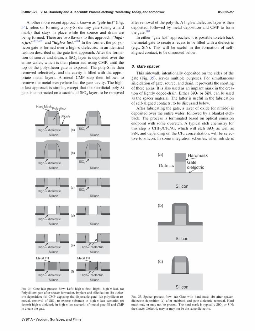
Another more recent approach, known as “gate last” (Fig.34), relies on forming a poly-Si dummy gate (using a hard
mask) that stays in place while the source and drain are
being formed. There are two flavors to this approach: “high-j first”276,281 and “high-j last.”281 In the former, the polysi-
licon gate is formed over a high-j dielectric, in an identical
fashion described in the gate first approach. After the forma-
tion of source and drain, a SiO2 layer is deposited over the
entire wafer, which is then planarized using CMP, until the
top of the polysilicon gate is exposed. The poly-Si is then
removed selectively, and the cavity is filled with the appro-
priate metal layers. A metal CMP step then follows to
remove the metal everywhere but the gate cavity. The high-
j last approach is similar, except that the sacrificial poly-Si
gate is constructed on a sacrificial SiO2 layer, to be removed
after removal of the poly-Si. A high-j dielectric layer is then
deposited, followed by metal deposition and CMP to form
the gate.281
In either “gate last” approaches, it is possible to etch back
the metal gate to create a recess to be filled with a dielectric
(e.g., SiN). This will be useful in the formation of self-
aligned contact, to be discussed below.
3. Gate spacer
This sidewall, intentionally deposited on the sides of the
gate (Fig. 35), serves multiple purposes. For simultaneous
silicidation of gate, source, and drain, it prevents the shorting
of these areas. It is also used as an implant mask in the crea-
tion of lightly doped-drain. Either SiO2 or SiNx can be used
as the spacer material. The latter is useful in the fabrication
of self-aligned contacts, to be discussed below.
After fabricating the gate, a layer of oxide (or nitride) is
deposited over the entire wafer, followed by a blanket etch-
back. The process is terminated based on optical emission
endpoint with some overetch. A typical etch chemistry for
this step is CHF3/CF4/Ar, which will etch SiO2 as well as
SiN, and depending on the CF4 concentration, will be selec-
tive to silicon. In some integration schemes, when nitride is
FIG. 34. Gate last process flow: Left: high-j first; Right: high-j last. (a)
Polysilicon gate after spacer formation, implant and silicidation; (b) dielec-
tric deposition; (c) CMP exposing the disposable gate; (d) polysilicon re-
moval, removal of SiO2 to expose substrate in high-j last scenario; (e)
deposit high-j dielectric in high-j last scenario; (f) metal gate fill and CMP
to create the gate.
FIG. 35. Spacer process flow: (a) Gate with hard mask (b) after spacer-
dielectric deposition (c) after etchback and gate-dielectric removal. Hard
mask may or may not be present. The hard mask is typically SiO2 or SiN;
the spacer dielectric may or may not be the same dielectric.
050825-27 V. M. Donnelly and A. Kornblit: Plasma etching: Yesterday, today, and tomorrow 050825-27
JVSTA - Vacuum, Surfaces, and Films

used and it may be desired not to expose the Si substrate to
the plasma, a thin layer of oxide is formed before the nitride
deposition, and the etchback may consist of one or two steps,
depending on the thickness of the nitride. The last step,
selective to SiO2, is carried out in a CH3F (or CH2F2) con-
taining plasma that can be adjusted to obtain high nitride:ox-
ide selectivity. The oxide layer can then be removed,
exposing the silicon substrate below.
4. Contacts
In this step, contacts are opened both to the gate and sili-
con substrate. If the first dielectric layer is planar, the
depths of these contacts can be significantly different,
depending on whether the contact is to be made to the gate
or source and drain. Therefore, the selectivity to the gate
material has to be high. The chemistries used for this step
are usually C4F8, C5F8, or C4F6 based, and typically, a me-
dium density plasma such as in a MERIE or multiple-
frequency capacitively coupled etcher is used. A slightly
tapered profile (88�–89�) is often desired to facilitate a
good contact metal-fill. ARDE control is extremely impor-
tant in this step. Although this step calls for equal size
openings, there could be slight variability across the wafer.
In addition, since the final aspect ratio of contacts to the
source and drain regions can be considerably higher than
the one to the gate, any etch rate reduction due to ARDE
will inevitably lead to a long overetch of contacts to the
gate (this is one motivation for using elevated source and
drain regions). Selectivity to the underlying layer (Si, SiN,
or silicide) is controlled by the thickness of the fluorocar-
bon film.282 When the contact is terminated on silicide, ex-
cessive exposure of the silicided source and drain to ion
bombardment can lead to junction degradation. This is gen-
erally addressed by a highly selective etch process that
relies on a thick fluorocarbon layer for protection. In some
integration schemes, an etch stop layer such as SiNx covers
the silicided gate, source, and drain, and a “soft” etch is
used to clear all contacts simultaneously with minimal over-
etch. This approach is also used to form a borderless-con-
tact,283 where the contact to source or drain may overlap
the isolation region and excessive oxide overetch is undesir-
able. When SiNx is used for the etch-stop layer, a number
of fluorocarbon gases can be used for etching; when high
selectivity to SiO2 is desired, either CH3F or CH2F2 can be
used for the nitride etch.
5. Self-aligned contacts
In many instances, such as memory devices, it is desirable
to have the contact to source or drain extremely close to the
gate. Unfortunately, due to misalignment, the printed contact
may overlap the gate, and eventually, once the contact is
filled with metal, the gate and source (or drain) will be
shorted. This can be overcome by encapsulating the gate
with a dielectric resistant to the SiO2 etch chemistry used for
opening the contact. Using SiN as the hard mask and spacer
will achieve this goal.283 The etch chemistry used for this
step is typically C4F8 based which can be tuned to achieve
high selectivity with respect to the nitride.282,284 Once the
SiO2 is cleared, a short step to remove the SiN and expose
the source or drain is then performed (Fig. 36).
FIG. 36. One of many ways of self-aligned contact formation. (a) Gate is
encapsulated with a blocking material that could be, for instance, LPCVD
Si3N4, plasma CVD nitride or another blocking material. (b) A thin layer of
blocking material is deposited. (c) First dielectric (usually BPSG) is depos-
ited and planarized. (d) Lithography step to pattern contacts that could be
misaligned. ARC, if used, is not shown. (e) Etching of BPSG selective to
the blocking layer. (f) Etching of the blocking layer to expose the silicided
source or drain and stripping of the resist.
050825-28 V. M. Donnelly and A. Kornblit: Plasma etching: Yesterday, today, and tomorrow 050825-28
J. Vac. Sci. Technol. A, Vol. 31, No. 5, Sep/Oct 2013

6. Aluminum
Aluminum based alloys were the dominant conductors for
interconnect in VLSI circuits before the introduction of cop-
per, although other metals, such as tungsten,263,285 have been
used occasionally. The aluminum alloys usually contain
small amount of silicon and/or copper—the former to
improve contact resistance when contact is made to the sili-
con substrate and the latter to control electromigration.286
Since copper does not form volatile compounds with the
chemistries used for aluminum etching (at the standard oper-
ating temperatures), its concentration is limited to less than
5%. When the Al layer is “sandwiched” between TiN layers,
the same chemistry is used to etch the TiN layers (and the Ti
that is used as an adhesion layer below the lower TiN layer)
with possible variation of process conditions tailored for
each layer.
Al will etch spontaneously in Cl2 gas, but the presence of
surface oxide inhibits etching. BCl3/Cl2 mixtures287,288 are
commonly used for etching of Al, usually in a high-density
plasma reactor, such as an ICP or ECR system. CCl4,288
SiCl4,288 and BBr3 (Ref. 289) feed gases have also been used
less frequently. The role of BCl3 is to remove the native ox-
ide on the aluminum,290 scavenge any moisture in the cham-
ber that may inhibit the etch process, and possibly to inhibit
sidewall etching.291 The interaction of the plasma with pho-
toresist leads to formation of a layer on the sidewall that will
prevent lateral etch of the aluminum,292 but may lead to sub-
sequent corrosion (discussed below). Sometimes an additive
to the feed gas helps in the formation of sidewall passivation
and can also be used to taper the metal lines. Typical addi-
tives are N2 and CHF3,227 but other polymer-forming addi-
tives have been used as well [e.g., CHCl3 (Ref. 293)].
Although the additive may have a positive effect on the
etched profile, it can cause particulate formation on the wa-
fer due to the flaking off of deposits from the chamber walls.
Therefore, the amount and type of the additives are impor-
tant in establishing the optimum tradeoff between a desired
profile and minimum wall deposits.
A hard mask can also be used for the pattern transfer. It
has the advantage of minimized variation between isolated
and nested aluminum lines, but since a major component of
the etching process, the eroding photoresist, is absent, the
etching process has to be modified. Etching in a low pressure
(�2mTorr) Cl2/HCl/N2 plasma has been used successfully to
pattern an aluminum stack consisting of TiN/Al/TiN/Ti.230
Etching uniformity is one of the challenges in aluminum
etching.288 Generally, the etch rate at the edge of the wafer
is higher than the center and the metal is cleared in “bulls-
eye” pattern. However, by process optimization and the use
of focus-rings, the effect can be minimized.
Postetch corrosion is a major concern and it can be either
purely chemical or galvanic. The chemical corrosion is asso-
ciated with residual chlorides present on the wafer, especially
on the sidewalls. Although during etching the wafer is heated
to 50–70 �C to help volatilize the etch by-products, some
AlCl3 is embedded in the sidewall deposits, leading to chemi-
cal reactions with moisture in the air294
AlCl3 þ 3H2O ! AlðOHÞ3 þ 3HCl; (24)
AlðOHÞ3 þ 3HClþ 3H2O ! AlCl3 � 6H2O; (25)
2AlCl3 � 6H2O ! Al2O3 þ 9H2Oþ 6HCl: (26)
Al is also consumed by aqueous HCl
2Alþ 6HCl ! 2AlCl3 þ 3H2: (27)
The process continues to corrode the aluminum, creating
“worm”-like residues that are easily observed in an optical
microscope (Fig. 37). The standard procedure to avoid
chemical corrosion is to minimize sidewall deposits, heat the
wafer during etching to the maximum temperature that will
not reticulate the photoresist, and use a passivation step,
combined with a partial or complete stripping of the photore-
sist. The passivation/strip is carried out by transferring the
substrates in a load-lock, under vacuum, to a separate cham-
ber designed specifically for that purpose (in earlier batch
metal etchers, resist strip was carried out in-situ using an ox-
ygen plasma with small amount of fluorine containing
gas,227 with the intention to convert the chlorides to noncor-
rosive fluorides). The passivation step is intended to convert
the residual chlorides to volatile HCl and is accomplished by
hydrogen-containing plasmas, typically water vapor.295
Additional steps to reduce chemical corrosion are to heat the
wafer after the passivation step on a hot stage in the etch
tool, keeping the wafer under vacuum until the entire lot is
etched, water rinse immediately after venting to dissolve any
residues that are left, and chemical sidewall removal, fol-
lowed by another resist ashing step to insure complete resist
removal. Wafers should be kept in a dry-box before a cap-
ping oxide layer is deposited. The time interval between
completion of the etch and the deposition step should be
short, preferably less than 24 h.
Galvanic corrosion takes place when a galvanic cell is
formed between two dissimilar metals in the presence of an
electrolyte. The two metals in this case are the aluminum
metal and the TiN layer(s) if used, and the electrolyte is the
FIG. 37. Aluminum corrosion. The reaction by-products of the reaction
between the chlorine-based residues, moisture, and aluminum are evident on
top and the side of the etched metal lines. See text for details.
050825-29 V. M. Donnelly and A. Kornblit: Plasma etching: Yesterday, today, and tomorrow 050825-29
JVSTA - Vacuum, Surfaces, and Films

residual chlorides dissolved in water. This galvanic corro-
sion looks different than the chemical corrosion described
above and is characterized by voids in the aluminum, while
the TiN layer(s) is (are) intact. Usually, the TiN is oxidized,
preventing the formation of the galvanic cell; however, if
there are discontinuities in the film the cell can form, and of-
ten, galvanic corrosion is observed in a small number of
sites. The galvanic corrosion is prevented by minimizing
sidewall deposits, and a postetch rinse in an adequate
amount of water: quick-dump-rinse or overflow-rinse are
preferable to spin-rinse.
The major component in prevention of the two type of
corrosion is the minimization of sidewall deposits. However,
these deposits are necessary for anisotropic etch. The opti-
mized etch process has to take into account these diametri-
cally opposite requirements: just enough sidewall deposits to
prevent undercut, but not enough to trap large amounts of re-
sidual chlorides.
7. Damascene structure
Modern metallization schemes utilize copper wiring
inlaid in a dielectric,296,297 producing structures similar to
damascene ornaments, where precious metal is inlaid in
another metal.298
Since metallization schemes involve a large number of
metal layers, the entire structure is repeatedly planarized at
every level. The first dielectric level, encapsulating the
active area, is doped SiO2 glass with metal (e.g., tungsten)
filled contacts to the source, drain, and gates. All subsequent
dielectric layers consist of low dielectric-constant material,
such as organosilicate glass, which was solid in early imple-
mentations, and porous in subsequent technologies. The
etching is accomplished with fluorocarbon-based plasmas
and the F:C ratio is adjusted to minimize residues. Trenches
(for intralevel interconnect) and vias (for interlevel intercon-
nect) are formed within these layers, to be filled in subse-
quent steps with copper (in early versions with aluminum)
and planarized by CMP. The resulting structure is a planar
surface on which the next level is to be built in a similar
fashion.
In a single-damascene scheme, contacts are made first to
the level below through vias formed within the dielectric, to
be filled with metal and polished to achieve planarity. The
intralevel connection is achieved by another deposition of
dielectric in which trenches are formed and filled with metal
in a similar fashion described above. The more common pro-
cess, however, is the dual-damascene scheme, where vias
and trenches are etched before the metal fill step.
There are a number of approaches to create a dual-
damascene structure with and without an intermediate etch
layer that provides an etch-stop for the trench etching. The
“via first” approach shown in Fig. 38(a) has evolved with
time and has been the preferred implementation of dual-
damascene structures. The version shown in this figure
shows more recent implementation of the structure where no
trench etch-stop layer is present within the low-j dielectric.
In this approach, the via is etched to completion, resist is
stripped (discussed below), followed by lithographic and
etch steps to form the trench. A planarizing layer, capping
layer (both absent in early implementations) and ARC are
also shown. The role of the planarizing layer is to smooth
the topography and, combined with the capping layer, it ena-
bles the use of a thin imaging layer. The pattern is first trans-
ferred to the capping layer (which could be either SiO2 or
SiNx, serving as a pattern-transfer layer) followed by a pat-
tern transfer to the planarizing layer. The etch chemistry for
the latter step is either O2 or CO2 based; the latter gives a
more anisotropic profile than the former. Sometimes the
ARC layer can serve in dual role as an antireflective layer as
well as a pattern-transfer layer.
FIG. 38. (Color online) Dual damascene process flow. Left: Via first, trench
last. (a) Via patterning on top of ARC and a cap layer; (b) Via pattern trans-
fer and resist strip; (c) Trench patterning utilizing a planarizing layer to
smooth the topography; (d) Trench pattern transfer with partial removal of
the planarizing layer in the vias; (e) Complete removal of the planarizing
layer, resist stripping, and barrier etch. Right: Trench first, via last. (a)
Trench patterning on top of cap layer and ARC; (b) Trench pattern transfer,
stopping on an etch-stop layer; (c) Via patterning; (d) Via pattern transfer,
resist strip and barrier etch.
050825-30 V. M. Donnelly and A. Kornblit: Plasma etching: Yesterday, today, and tomorrow 050825-30
J. Vac. Sci. Technol. A, Vol. 31, No. 5, Sep/Oct 2013

In the “trench first” approach [see Fig. 38(b), shown with
a trench etch-stop layer], after the deposition of the low-jdielectric, trenches are patterned first by standard litho-
graphic technique and etched to a finite depth into the dielec-
tric. After resist removal, another lithographic step defines
the via, and the etch process continues all the way to form
the contact to the metal level below. A capping layer on top
of the metal below is then etched in a low-bias process to
reduce sidewall formation.
Since oxygen plasmas can degrade the low-j dielec-
tric,299 resist ashing is not performed in an oxygen plasma
asher, but rather in a medium-density plasma (e.g., capaci-
tively coupled plasma etcher), using plasmas with low-
oxygen concentration or other chemistries, such as N2/H2
based chemistry. Regardless of the ashing process used,
some degradation of the dielectric is observed,299,300 which
is substantial for ultra low j (j< 2.3) dielectrics. Therefore,
newer dual-damascene schemes such as the trench first metal
hard mask (TFMHM) approach attempt to minimize expo-
sure of the low-j dielectric to resist-stripping plasmas.
TFMHM is the latest evolution in dual-damascene imple-
mentation, where the low-j dielectric is etched with a metal
hard mask. In this approach, metal (usually TiN) is patterned
first (Fig. 39) with a trench pattern and etched. After resist
strip, the vias are patterned and partially etched into the
dielectric, followed by resist strip, and simultaneous etching
of trenches and vias. There are a number of advantages to
this method, such as self-aligned vias,301,302 and reduced
degradation of the low-j dielectric associated with resist
stripping.303 However, other issues have to be dealt with,
such as hard mask etching, and a clean etch of the dielectric
without residues associated with sputtered hard mask
material.301,302,304
8. FinFETs
To achieve higher performance at lower voltages, three
dimensional transistors are finding their way into advanced
devices. The fabrication involves creating “fins” in the sub-
strate on which field effect transistors are built.305–307 The
gate wraps around the fins (Fig. 40) and depending on the
number of the sides of the fin used to form the device, bigate
or trigate FETs are created.308 Figure 40 depicts a trigate de-
vice, while a bigate FET will have an insulator on top of the
fin. There are two approaches for fabricating these devices,
depending on the substrate—SOI or bulk silicon. These two
approaches are shown in Figs. 40(a) and 40(b) for SOI and
bulk silicon, respectively. The approach taken will depend
on a number of factors, one of which is the cost of the sub-
strate.309 The gate width for a single-fin tri-gate device will
be the sum of twice the height plus the width. Multiple fins
can be used to achieve wider gates.
The height of the fins depends on the technology-node.
For instance, at the 22 nm node, the fin is about 8 nm wide at
its midheight and 34 nm high.310 With SOI substrates, where
the device-layer thickness equals the targeted fin-height,
trench isolation is performed first, and then the fins are
etched into the device layer, stopping on the buried-oxide
layer. If bulk silicon is used, the fins are etched at the same
time as the isolation trenches, using a hard mask. Ideally,
vertical fins are desired, and the etch is carried out in two
step—the first to create the vertical profile needed for the
fins, followed by an etch step that creates a tapered profile
needed for the trench.311 After oxide deposition and planari-
zation, the oxide in the fin areas is etched back to the appro-
priate depth to expose the fins. Since the sidewalls of the fins
are used for the active devices, surface roughness associated
with the etch can lead to creation of interface-traps. This can
be addressed by the etch process311 and/or postetch surface
treatment.
Once the fins are created, gate formation follows with ei-
ther “gate first” or “gate last” approaches. The only differ-
ence between formation of planar and FinFET gates is the
FIG. 39. (Color online) Dual damascene process flow—TFMHM. (a) Trench
patterning on top of ARC, pattern-transfer layer (oxide), planarizing layer,
and metal hard-mask; (b) Trench pattern in metal hard mask; (c) Via pattern-
ing; (d) Via pattern transfer into low-j dielectric; (e) Trench etching into the
low-k dielectric, using the metal as a mask and barrier removal. Metal hard
mask is removed in subsequent steps.
050825-31 V. M. Donnelly and A. Kornblit: Plasma etching: Yesterday, today, and tomorrow 050825-31
JVSTA - Vacuum, Surfaces, and Films

long overetch-steps associated with the topography. In the
gate-first approach, both metal-gate and hard mask have to
be cleared,312 while in the gate-last approach, the sacrificial
polysilicon has to be etched in its entirety without penetrat-
ing the SiO2 layer below. In both cases, the spacer formed
before the source and drain construction must be cleared
from the walls of the fins, while leaving the gate (or sacrifi-
cial gate) protected.
Evolution to more complex 3D devices is expected. The
“Pi-Gate,” “Omega-FET,” and “Gate-All Around” as well as
the use of new materials313,314 will, no doubt, pose some
integration and etching challenges in the future.
D. Micromachining
Silicon-based MEMS can be fabricated by techniques
similar to those used in silicon IC fabrication. Although
ceramics, polymers, and metals are also MEMS materials,
the focus of this review is on silicon-based systems only. As
will be discussed below, etching techniques used for bulk
micromachining have been adopted for etching TSV to facil-
itate electrical connections to the backside of the wafer.
Some MEMS involves fabrication of devices only on the
surface of a silicon wafer, and the techniques used to fabri-
cate these devices fall into the class of surface micromachin-
ing. Bulk micromachining involves utilizing a greater portion
of the silicon wafer, typically more than 10lm of silicon.
1. Surface micromachining
The etch processes used for surface micromachining are
similar, with some modifications to etch processes used in
IC fabrication. Cl2 or HBr based processes are used to etch
silicon, but in most cases, high selectivity to oxide is not
required. CD control is important in some cases, and control-
ling CD when high aspect-ratio structures are desired could
be quite challenging, similar to that encountered in the fabri-
cation of trench capacitors in DRAMs.
In many cases, especially when high-aspect ratio struc-
tures are to be etched, a hard mask (SiO2 or SiNx) is used.
For these applications, SF6-based chemistry can be used.
Profile control is a challenge, since SF6 will tend to etch Si
isotropically, but with the proper additive for sidewall passi-
vation (e.g., C4F8, Cl2, or HBr), anisotropic profiles can be
achieved (Fig. 41). If the process is terminated on an etch-
stop layer, such as the BOX layer used in SOI wafers, the
overetch step usually differs from the main etch step to avoid
undercut during the overetch. This is accomplished either by
modifying the gas flows and/or bias conditions, or switching
to another etch chemistry, such as Cl2/HBr.
2. Bulk micromachining
Silicon bulk micromachining requires etching to depths
greater than 10 lm. It is commonly referred to as “deep reac-
tive-ion-etching” (deep RIE or DRIE) and etch tools are
modified high plasma-density etchers, with additional fea-
tures to facilitate high etch rates with some degree of profile
control.
To achieve high etch rates, SF6 is the source gas, some-
times with the addition of O2 primarily to reduce the chances
of sulfur build-up in the exhaust line. To obtain anisotropy,
the sidewalls of the features being etched must be passi-
vated. One approach is to cool the substrate315–317 to typi-
cally below 220K (Ref. 317) and slow the rate of isotropic
etching by F-atoms (see Fig. 15). (Ion-assisted etching proc-
esses typically have little or no temperature dependence.)
The cold temperatures also lead to a buildup of SiOxFy by-
products on the sidewalls, also suppressing isotropic etch-
ing.315,317 It produces smoother sidewalls than the switched
process described next, but sufficient time is needed for wa-
fer cooling and warming before and after the etch, respec-
tively. Once the wafer is warmed, the protection layer is
volatilized, and if additional etch time is needed after
FIG. 40. FinFET with (a) SOI substrate and (b) bulk silicon substrate. The
gate and the gate dielectric wrap the fins formed by etching silicon. The
structure shown is a trigate, where three surfaces of the fin are used to form
the gate.
FIG. 41. Surface micromachining. The height of these features is 12lm, and
the minimum dimension is 0.25lm.
050825-32 V. M. Donnelly and A. Kornblit: Plasma etching: Yesterday, today, and tomorrow 050825-32
J. Vac. Sci. Technol. A, Vol. 31, No. 5, Sep/Oct 2013

postetch inspection, undercutting will occur due to the ab-
sence of a protection layer on the sidewall.317
A second method, known as the Bosch Process,318,319 is a
switched-gas process that utilizes alternate steps of etching
with SF6 as the feed gas, and polymer deposition, usually
with c-C4F8 as the feed gas. The switched process is the one
more commonly used, and it requires fast acting mass-flow-
controllers to switch between etch and deposition steps,
which occur every few seconds. An ICP etching tool is com-
monly used for the process and bias power is turned on only
during the etch step and is kept low—only a few watts.
Source power during the etch step depends on the total gas
flow (to be discussed below). During the deposition step,
polymer is being formed on the horizontal surface as well as
on the sidewall. The etch step then removes the polymer
from the horizontal surface, and proceeds with etching of sil-
icon, while the remaining polymer on the sidewall, even
though it is being eroded, provides protection against lateral
etching. The resulting sidewalls show striations (Fig. 42),
and may be an issue when smooth sidewalls are needed (e.g.,
mirror surface).
It is desirable to use etch mask and etch stop materials (if
needed) that are resistant to the fluorine plasma. SiO2,
Al2O3, and photoresist etch masks etch very slowly with
selectivities with respect to silicon of 250:1, >10,000:1, and
50:1, respectively.320 SiO2 and Al2O3 can also be used as an
etch stop material. Care must be used when choosing the
etch stop and etch mask material such that the material cho-
sen does not sputter during the etch to deposit nonvolatile
products. This will cause “grass” to form in the etched areas
due to micromasking.321
In many instances, the etch depths are hundreds of lm,
sometimes the full thickness of a silicon wafer (7256 25 lmfor 200mm diameter wafer). Therefore, a high etching rate
is important. Etching rates can be increased by increasing
gas flow, coupled with an increase in source power (Fig. 43).
However, selectivity is reduced (the Si etching rate increases
at a slower rate than does erosion of the mask), and it is
claimed that this is due to increased ion flux.229 Plasma
source power affects ion energy distributions as well as ion
flux. Ion-flux/energy control, offered on some etchers, is the
key to achieving high etching rates without the adverse
effects such as degraded selectivity mentioned above. One
approach is to use pulse shape biasing.322,323
Etching of Si for MEMS devices has many of the same
issues as for Si integrated circuit manufacturing. Etch rates
are governed by the flux of reactants reaching the substrate
surface. Therefore, etch rates drop as the total silicon area
exposed to the plasma is increased (i.e., loading effect—Fig.
44). Therefore, Si etch rates for via patterning will be higher
than for trench patterning. Although absolute etch rate is an
important consideration, uniformity of the etching rate is im-
portant as well. Etching nonuniformity is less important
when an etch stop layer is used, but selectivity and thickness
of the etch stop layer must be adequate to offset the etching
nonuniformity.
Another important structure in advanced MEMS as well
as integrated circuits is a TSV, also known as through-wa-
fer-via.324 In MEMS fabrication, it enables electrical routing
on the back of the wafer, freeing important “real estate” on
the front of the wafer. The structure can also be used for
bonding various MEMS modules to create a highly complex
system, which combines MEMS and low and high-voltage
control circuitry in one assembly.325 In IC fabrication TSVs
are used for 3D interconnects. There are number of ways to
create electrical interconnect using TSV structures. They all
FIG. 42. Scalloping associated with a switched (Bosch) process. The scallops
are the result of alternate etch and deposition steps.
FIG. 43. Si etching rate in an SF6 plasma as a function of source power and
flow-rate. Etching rates are given in lm/min. The “bubble” sizes are propor-
tional to the etching rate.
FIG. 44. Etch depth and uniformity (5 min in SF6 based etch) as total area of
wafer exposed to plasma is increased. Process is not optimized for uniform-
ity [after Bogart et al. (Ref. 321)].
050825-33 V. M. Donnelly and A. Kornblit: Plasma etching: Yesterday, today, and tomorrow 050825-33
JVSTA - Vacuum, Surfaces, and Films

involve creation of vias, depositing an insulating layer on the
sidewalls, filling the via with conducting material, wafer
thinning and stacking multiple wafers to create the 3D
device.
E. MRAM and FeRAM
Magnetoresistive and ferroelectric random-access-mem-
ory devices known as MRAM and FeRAM (or FRAM),
respectively, are classes of nonvolatile RAM devices made
of materials that do not form volatile compounds when
etched in plasmas near room temperature.
MRAM memory cells utilize magnetic tunnel junctions
to form a nonvolatile storage cell, integrated into the back-
end processing of a CMOS device. Multiple stacked thin
films form the cell. At a minimum, there are two magnetic
layers separated by a thin dielectric layer. The magnetic
moment orientation of one of the magnetic layers is fixed
while the orientation of the moment of the second magnetic
layer is free and it could be set by the control circuitry to be
either parallel or antiparallel to the orientation of the fixed
moment. The tunneling magnetoresistance will change based
on the orientation of the moment of the free layer and that
can be sensed by the CMOS circuitry. In reality, there are
additional layers used to pin the moment of the fixed layer
and prevent it from changing orientation during a “write”
operation. The end result is a stack of thin (order of 1 nm or
below) layers with Al2O3 (Ref. 326) [or MgO (Ref. 327)] as
the tunneling dielectric and magnetic materials such as Ni,
Fe, Co, and their alloys, Ru, as well as IrMn or PtMn that
serve as an antiferromagnetic pinning material (Fig. 45).
Unlike the etching of ferroelectric devices (see below), the
etching of these stacks cannot be carried out at elevated tem-
peratures due the instability of the alloys used. Chlorine, bro-
mine, and fluorine based chemistries can be used266,328,329
to create compounds that are sputtered away, but postetch cor-
rosion associated with residues on the wafer must be
addressed.266 In some instances (NiFeCO), enhanced etch-rate
in Cl2/Ar plasmas with UV illumination has been observed,330
but the mechanism is not well understood. Alternately, a
CO/NH3 mixture has been demonstrated as another option,
since it can form carbonyls that are volatile,331–334 with some
enhancement with the addition of Xe.335 This process is not
entirely chemical, however, and sputtering does take place, as
evident from the thick sidewalls of redeposited sputtered
material.336 Another option to avoid patterning tough-to-etch
materials is to use damascene structures. In this scenario,
cavities are etched into the dielectric, and a stack of all of
the above materials is deposited followed by planarization
by CMP.266 Although this solution seems simple, it basically
transfers the difficulty from etch to the process of
chemical–mechanical-polishing. There may be some other
integration issues associated with this approach.
FeRAM, known also as FRAM or F-RAM, is a random
access memory, where the memory cell consists of one ca-
pacitor and one access transistor, similar in structure to a
DRAM. The dielectric in the capacitor is a ferroelectric ma-
terial such as PZT, while materials such as Ir and IrO2 are
used for the electrodes. Etching of the stack at temperatures
above 350 �C in a capacitively coupled plasma reactor with
magnetic confinement yielded vertical profiles.63 Chlorine
and fluorine based gases together with oxygen and argon
were part of the etch chemistry.
VI. FUTURE
It has been said that “Studying the past is no sure guide to
predicting the future.337” It has also been said, allegedly by
Niels Bohr (and more recently, in a slightly different manner
by others, including Yogi Berra), that “Prediction is very dif-
ficult, especially about the future.338” Nevertheless, for an
industry with annual sale of roughly $300� 109,339 some ju-
dicial assessment of future technologies is needed. The semi-
conductor industry, like others, develops and lives by
roadmaps. The corresponding roadmap is the International
Technical Roadmap for Semiconductors (ITRS, published in
earlier editions by the Semiconductor Industry Association
as the National Technical Roadmap for Semiconductors),340
revised annually, with complete reports published biennially.
Over time, changes in the ITRS may be significant; however,
it is a blueprint for evolution of devices, technology, and
processes, and it gives guidance to research and development
efforts. The discussion below is based loosely on future de-
vice and technology requirements, covered in the relevant
chapters of the 2011 edition of the ITRS.341–346
A. Patterning
Aside from advances in lithographic techniques, such as
using next-generation-lithography tools, there are numerous
techniques to achieve sub-lithographic features. Some
involve pure lithographic methods, such as double-expo-
sure,346 some rely on combinations of lithography and etch-
ing, and other approaches use solely etching techniques to
define features smaller than the capability of the lithographic
tool. A number of methods have been proposed; some are
beginning to find their way into manufacturing, while some
are at the early stage of development and assessment of their
capabilities and limitations. Some techniques are more
FIG. 45. MRAM capacitor structure. The free, fixed, and pinned layers are
usually alloys of Co, Ni, and Fe. The fixed, pinned and ruthenium layers
form a synthetic antiferromagnet (SAF) layer. The antiferromagnetic (AF)
pinning layer (IrMn or PtMn) is used to prevent the SAF from responding to
write operations [after Engel et al. (Ref. 326)].
050825-34 V. M. Donnelly and A. Kornblit: Plasma etching: Yesterday, today, and tomorrow 050825-34
J. Vac. Sci. Technol. A, Vol. 31, No. 5, Sep/Oct 2013

appropriate for less dense logic devices, while others are
intended for dense structures.
The method of trimming is discussed in the section on
gate patterning, and it has been in use in production for a
number of years. It is adequate for isolated lines, but not for
creating dense patterns. Aside from CD control issues, there
are also limitations associated with thinning of the resist as
the result of the trimming operation.
The method of double patterning (DP)346–348 utilizes two
lithography and etch steps to pattern a single layer, which is
then used to transfer the pattern to the target layer (e.g., gate,
trench, etc.). It is often referred to as the litho-etch-litho-etch
(LELE) method.346 The technique is illustrated in Fig. 46;
after the first lithographic step [Fig. 46(a)], a hard mask is
etched, followed by resist strip [Fig. 46(b)] and another lith-
ographic step [Fig. 46(c)], where additional features are
printed and etched to create a dense pattern after the resist is
stripped [Fig. 46(d)]. The resulting hard mask is then used to
etch the target layer [Fig. 46(e)].
Spacer double patterning approaches come in two vari-
eties, positive and negative tones. In the positive tone approach
(known also as self-aligned double patterning349–351 or side-wall image transfer352), the sidewall-spacer is used as the hardmask for pattern-transfer to create features well under the litho-
graphic capability of the lithographic tool. The concept is not
new; it was first used by utilizing sidewall deposits formed dur-
ing trilevel etching,353 where the etched hard-baked resist was
ashed away, leaving the sidewalls as the mask for the pattern
transfer.354 Similarly, small platinum features, 50 nm wide,
were fabricated by sputtering away platinum films deposited
on amorphous-silicon sacrificial structures that were subse-
quently removed by chemical dry etching.355
In the positive tone approach, the size of the features is
controlled by the CVD and etch processes, while the space
between the features is determined by lithography. The
method, shown in Fig. 47, can be used when all the features
are of equal size, such as the fins in FinFETs. The first step
in using this technique is to create structures (mandrels), on
top of the target layer [Fig. 47(a)] that will be used to con-
struct the sublithographic features. After CVD and etch,
sidewall-spacers are created [Fig. 47(b)], followed by the re-
moval of the mandrels [Fig. 47(c)], pattern transfer and
spacer removal to create the desired structure in the target
layer [Fig. 47(d)]. The mandrel material will depend on the
application. To fabricate the fins for FinFETs, for instance,
the mandrel could be amorphous carbon, patterned with pho-
toresist (possibly after trimming, discussed above, and using
SiO2 or SiN as the pattern-transfer layer), while the spacer
material is SiO2 or SiN. The spacer remaining after the ash-
ing can be used as the hardmask for the pattern transfer
directly into the silicon to create the fins. Another applica-
tion of the technique is metal gates on high-j dielectrics.
FIG. 46. Double patterning (DP): (a) First lithographic step. (b) Hard mask is
etched, followed by resist strip. (c) Second lithographic step. (d) Hard mask
etched and resist stripped. (e) Pattern transfer to the target layer.
FIG. 47. Spacer double patterning—positive tone: (a) Create mandrels on
top of the target layer. (b) Form sidewall spacers by CVD and etch-back. (c)
Removal of the mandrels. (d) Pattern transfer and spacer removal to create
the desired structure in the target layer.
050825-35 V. M. Donnelly and A. Kornblit: Plasma etching: Yesterday, today, and tomorrow 050825-35
JVSTA - Vacuum, Surfaces, and Films

In the negative tone approach, dense features can be cre-
ated, and their widths need not be the same. In this case the
spacers are disposable.351,356 Following the formation of the
mask [e.g., SiO2, SiN, or polysilicon, Fig. 48(a)] on top of
the target layer (which could be either a device layer or a
hardmask used for the pattern-transfer to the device layer), a
spacer is formed by deposition and etchback [Fig. 48(b)]. A
layer of oxide is then deposited to fill the gap between the
feature [Fig. 48(c)], followed by etchback or CMP to expose
the spacers [Fig. 48(d)]. The spacers are then removed to
create a dense pattern shown in Fig. 48(e), which is then
used to transfer the pattern to the target layer. The choice of
materials will obviously depend on the application. Jung
et al. used the technique to create a dense pattern in a target
layer consisting of 50 nm SiON on top of 200 nm amor-
phous-carbon.356 In this case, the mask was 200 nm polysili-
con, the sacrificial spacer-sidewall was 20 nm fluorocarbon
and the gap-fill material was spin-on glass.
Self-aligned quadruple patterning (SAQP)349,357 is an
extension of the self-aligned double patterning described
above. In this case, the first mandrel is used to create a
denser pattern in a 2nd mandrel layer, as shown in Fig. 49.
After the formation of the first mandrel [Fig. 49(a)], spacers
are formed [Fig. 49(b)], and the mandrels are removed
[Fig. 49(c)]. The remaining features are then used to transfer
the pattern to the hard mask and form a second mandrel
[Fig. 49(d)]. After spacer formation [Fig. 49(e)], and man-
drel removal [Fig. 49(f)], the pattern is transferred to the tar-
get layer [Fig. 49(g)].
In another variation, self-aligned triple patterning is
claimed to offer some advantages over the other multipattern-
ing schemes.349,357,358 The technique involves the creation of
two consecutive spacers, the first of which is sacrificial. The
mandrels in this case are not sacrificial, and can be used, in
addition to the spacers, as the hard mask for the pattern trans-
fer. Details can be found in the references cited.
B. Linewidth roughness and line-edge roughness
Linewidth roughness (LWR) and line-edge roughness
(LER) are related quantities that affect CD control. LWR is
FIG. 48. Spacer double patterning—negative tone: (a) Create mandrels on
top of the target layer. (b) Create sidewall spacers by CVD and etch-back.
(c) Gap fill. (d) CMP or etch back to expose the spacers and the mandrels.
(e) Remove the spacers. (f) Pattern transfer to the target layer.
FIG. 49. SAQP: (a) Create first mandrels on top of a hard mask layer. (b)
Form sidewall spacers by CVD and etch-back. (c) Remove first mandrels.
(d) Use the features created by the previous step for pattern transfer into the
second mandrel layer. (e) Form sidewall spacers by CVD and etch-back. (f)
Remove second mandrels. (g) Transfer pattern to the target layer.
050825-36 V. M. Donnelly and A. Kornblit: Plasma etching: Yesterday, today, and tomorrow 050825-36
J. Vac. Sci. Technol. A, Vol. 31, No. 5, Sep/Oct 2013

a measure of variation in width of the line expressed in 3r,while LER is the variation from a straight line along the
edge of the line (also expressed in 3r).359,360 The guidelinesfor low-frequency LWR are generally less than 8% of the
CD,346 and it can occur immediately after the resist is pat-
terned, with amplification during the pattern-transfer.361
Low-frequency line-edge roughness is linked to fluctuation
in CD,359,360 while high frequency LER in polysilicon gate
can lead to enhanced lateral diffusion, ultimately causing
reduced channel-length.362 The roughness is an issue that is
becoming more critical as CD decreases, since LWR does
not scale with linewidth shrink. In the etch process, it is asso-
ciated with plasma interaction with the photoresist,361 which
roughens the surface, thus causing edge roughness, espe-
cially if the resist is chemically amplified.363,364 Ion bom-
bardment, plasma radicals, and polymers deposited during
the etch are claimed to be contributors to the resist rough-
ness.363 Also, photons and heat have been shown to synergis-
tically cause LER.361,364 Although the etch process can be
tuned to reduce the effect,365 it is clear that more robust
resists are necessary in the future to reduce LWR and LER
in the patterned resist as well as in the postetch pattern.
Nonchemically amplified resists are claimed to be the solu-
tion for the problem, but they may present a different set of
challenges for the etching process. One option considered is
the use of inorganic resists,366 which, depending on the ma-
terial, may be easy or difficult to remove after the etch. For
instance, one candidate contains both Hf and Zr and exhibits
>7:1 SiO2:resist selectivity,367 so removal of the material af-
ter the pattern transfer may be a challenge.
C. New materials
Silicon continues to be the substrate material for the fore-
seeable future, but SiC is emerging as the material of choice
in some applications.368 In silicon devices, other materials
are expected to be incorporated in the future. Alternate chan-
nel materials with high mobility are of great interest,
and their integration to large-scale devices may be quite
challenging. The list of materials of interest is long and
includes n-InGaAs and p-Ge in the near future, and other III-
V materials, n-Ge, carbon nanotubes, and graphene in future
technologies.344 All of these materials are expected to be
grown epitaxially (there may be other options for gra-
phene369), but forming a good contact to some of these mate-
rials (e.g., graphene) is a major challenge.
The implementation of high-j materials as the gate
dielectrics has addressed the high leakage current density
associated with thin effective-oxide-thickness (EOT), but
future devices may require even higher-j materials [e.g.,
TiO2 (Ref. 344)] than the current Hf based dielectric to
reduce EOT even further. Removal of these materials from
the substrate with no appreciable damage will have to be
addressed.
Although there is some discussion on using carbon nano-
tubes345 as a potential interconnect material, in all likelihood
copper will be the conductor of choice for some time, and
the focus for improved performance will be the reduction of
the dielectric-constant of the interlevel dielectric. The pore-
volume in the dielectric is expected to increase, leading to jvalues below 2.0. Etching the highly porous material,
postetch-cleans as well as its integration into current metalli-
zation scheme are doable, but may not be simple extension
of current processes. One material is pure-silica-zeolite370
which, depending on its porosity, could reach j values below
2.3, but with an increase in leakage current. Alternately, a
nonporous low-j dielectric can be used. A polycarbosilane-
based dielectric with a j value as low as 2.32 and low leak-
age current is one choice.371 The advantage of this material
is that once it cured, it resists copper diffusion into the
dielectric (attributed to the lack of oxygen in the dielectric),
thus enabling copper metallization without the need for a
barrier material in the vias and trenches. As a result, lower
resistivity interconnects can be realized with this material
compared to a dielectric where a barrier material is
needed.342 A carbon-rich fluorocarbon material with k< 2
also has been reported.372 The material is deposited by a
plasma discharge of C5F8 and Ar. It exhibits good adhesion to
the SiCN barrier layer, and good thermal and mechanical prop-
erties. The ultimate goal for reduction of j value is a number
close to 1.0. This will be discussed in the following section.
High-j dielectrics have been introduced to DRAMs as
well to maintain the capacitance as the device dimensions
shrink. Current capacitor structures utilize TiN as the elec-
trode material with high-j insulator as the dielectric
(TiN/insulator/TiN or TIT structure).373 HfxAlyOz dielectrics
were used initially,373,374 but they have been replaced by
ZrO2/Al2O3/ZrO2 (ZAZ)373,375 at the 40–30 nm half-pitch
technology nodes, to achieve EOT of 6.3 A.375 Future
replacement with perovskite structure materials will have a
higher j value.376 Etching of these materials is not required,
since they are incorporated in a capacitor structure that cur-
rently requires formation of cylindrical cavities in oxide,
with no need to etch these dielectrics (see discussion on
structures below).
Other memory devices in the near future, phase-change
memories (PCM, known also as phase-change random
FIG. 50. (Color online) Ion energy distributions obtained in a pulsed ICP
with synchronous pulsed DC bias of a boundary electrode (Ref. 434).
050825-37 V. M. Donnelly and A. Kornblit: Plasma etching: Yesterday, today, and tomorrow 050825-37
JVSTA - Vacuum, Surfaces, and Films

access memory, or PRAM devices), utilize changes in resis-
tivity of chalcogenides in their amorphous and crystalline
states to create nonvolatile memories.340,344 These devices
are seen as a future replacement of Flash memory, and in
some applications, as replacements for DRAM and static
random access memory. PCM devices are already commer-
cially available for mobile applications, with endurance of
106 write-cycles in current product offering,377 and a poten-
tial of increased reliability in future devices (6.5� 1015
cycles in one recent publication).378
It seems that most of the new materials to be introduced
in future devices will not require new etching processes and
they will be incorporated into structures formed in traditional
materials.
D. New structures
The ITRS lists a large number of emerging devices that
are in different stages of research or development.
Obviously, only a small number will be commercialized. At
this stage, it is not clear what role plasma etching will play
in the fabrication of these devices. In the following discus-
sion, we will concentrate on structures where plasma etching
may be important.
3D structures are expected in most if not all devices in the
near and distant future. FinFETs are now used in manufac-
turing of advanced ICs and are expected to become more
ubiquitous. The current trigate structure is expected evolve
to “Pi-Gate,” “Omega-FET” and “Gate-All Around” struc-
tures (see discussion of FinFETs in Sec. VC). In forming
these structures, control of the damage to the underlying sub-
strate will be highly important. Various modifications of
FinFETs have been implemented for DRAM applications.
The combined structure of saddle FinFET (S-Fin)379 and
Recessed Channel Array Transistor380 or R-FinFET seem to
be the preferred structure for current and future generation
of DRAMs.381
The DRAM capacitor has evolved over time too. Since
minimum capacitance of roughly 25–30 fF per cell is
required regardless of the technology node (as determined
by the sensing circuit, data retention requirements, and sin-
gle disrupting events, such as alpha particles and cosmic
radiation382), the capacitor structure has evolved to maintain
this minimum value with reduction in the area occupied on
the device. The initial planar capacitor was replaced by a
trench382 and stacked capacitors.382,383 The latter has
evolved with time to a 3D, cylindrical-cavity structure383
with the use of high-j dielectrics. The capacitor structure is
expected to change to a pillar type as device dimensions and
dielectric thickness shrink further.344 Bonding of multiple
DRAM chips vertically (with the use of through-wafer-vias)
to form high-capacity devices is also expected.383–385
In interlevel metallization, the goal is to lower the dielec-
tric constant with the ultimate goal of j close to 1.0. One
way to achieve this is by using nonconformal interdielectric
deposition that will lead to void formation between the
metal lines.386–389 In this approach, the dielectric between
the metal interconnect is etched away, followed by the
nonconformal deposition of the dielectric. An alternate
approach is to use a sacrificial material to build the entire
metallization structure, to be removed (at least partially)
later-on,390 creating a structure that is generally devoid of
solid dielectric between the lines. Reactive gas can be used
to remove some sacrificial materials.387,391,392 Other sacrifi-
cial materials can be removed by thermal decomposition,
with the resulting gases diffusing through the capping
layer.393–395 Regardless of the method used, numerous etch-
ing, integration, packaging, and reliability issues must be
addressed before this scheme becomes viable.
Quantum computing is an area of active research that
promises to deliver future computing power far exceeding
what is available today.396,397 Some of the approaches are
based on a nuclear spin of 31P donor in silicon,398–400 quan-
tum dots,401–403 and ion traps,404–410 and many of the fabri-
cation steps are similar to the ones used in IC and MEMS
fabrication today.
Clearly, regardless the path chosen from the choices
above, device dimensions will continue to shrink, and the
requirements for high-fidelity pattern transfer as well as
reduction in damage and particle formation will become
ever more stringent. As new 3D structures are introduced,
selective and residue-free etch processes will be even more
challenging.
E. Improved processes and equipment
One obvious source of concern for future device technol-
ogies is the particles that may be generated in the chamber
and end up on the wafer before or during etching. Since the
size of particles must be much smaller than the smallest de-
vice dimension, the fraction of particles in a given size distri-
bution that qualify as “killer defects” keeps increasing over
time. Particles are generated by the process, as deposits flake
from the chamber walls and fall on the wafer. They can also
arise from erosion of materials in the chamber. Process gen-
erated particles can be addressed by frequent cleaning of the
chamber wall (e.g., between wafers), or by trapping the par-
ticles in a polymer coating.54 The approach taken will be
process dependent. Particles generated by the degradation of
material in the chamber can be mitigated by choice of better
materials and/or replacement of components in the chamber
at frequent intervals. Chamber materials, including coatings,
will likely become even more important in the future for
both particle generation and for consistency in etching
behavior over time.
Better control of ion and neutral fluxes as well as ion
energy will be required to address issues such as CD control,
ARDE, line-edge roughness, and lattice damage due to ion
bombardment. In addition, improvements in the precise con-
trol of amount of material removed and etch uniformity will
be needed.
Since vertical dimensions (with the exception of the pho-
toresist mask) do not decrease as much as the width of devi-
ces shrinks, aspect ratios of contacts and trenches continue
to increase. Therefore, ARDE control is important both to
compensate for variation in the lithography-defined features
050825-38 V. M. Donnelly and A. Kornblit: Plasma etching: Yesterday, today, and tomorrow 050825-38
J. Vac. Sci. Technol. A, Vol. 31, No. 5, Sep/Oct 2013

as well as changing aspect-ratio with time. In principle, lon-
ger etch-time may be used to compensate for the etch-rate
reduction; however, the thin photoresist may erode before
the etch process is complete. It has been shown that control
of the ion/neutral ratio is the key to reduction of aspect-ratio
dependent etch rate of dielectrics.215,217 This was accom-
plished by changing process parameters, such as pressure
and fluorocarbon feed gas fraction.217 However, these condi-
tions tend to lead to high polymer deposition, which can sup-
press etching entirely, and do not offer sufficient selectivity
to current thinner photoresist. Bias power pulsing seems to
offer an additional means for controlling ARDE,53,54 without
changing pressure or gas flows, by operating in an ion-
limited regime.162,411 In this case, the neutral flux stays
nearly constant, but ion-flux is controlled by the on/off cycle
of the bias. Although etching rates may still be decreased by
the increased aspect-ratio, the required longer etch times are
not prohibitive. With bias pulsing, photoresist erosion is
reduced more than the dielectric etching rates, increasing se-
lectivity to photoresist as compared to continuous-wave
plasmas.
As discussed above, line-edge roughness has been always
a concern, but it has become more acute as device dimen-
sions shrink. Roughness along the edges of photoresist has
been shown to be induced by a combination of exposure to
UV light, ion bombardment, and heat.80,412 Preliminary
results have shown53 that time modulation of neutrals, where
conditions are repeatedly switched from depositing polymer
on the sides of the photoresist (and tops) to etching, can pre-
vent rough edges on the photoresist. This is done while keep-
ing the ion flux constant.
Using pulsed plasmas may be the potential solution to
other concerns too, such as surface damage to the layer
exposed to the plasma. In the past, the solution has been to
remove the damaged layer either by chemical etching (e.g.,
downstream etching) or by oxidizing the surface and remov-
ing the oxide in HF solution. This loss of material is becom-
ing less tolerable now and will be too high a price to pay in
future device technologies.
Two general areas of research have re-emerged to address
many of these issues: time-modulated plasmas and neutral
beam etching. Pulsed plasmas have been an active area of
research for many years.413–430 In most of these early stud-
ies, the plasma-generating power was modulated; in a few
instances, pulsed bias was also investigated. RF or micro-
wave power is modulated at frequencies of typically
�10 kHz, and �50% duty cycle. Within �10 ls of the powerbeing turned off, Te drops from several eV to �1 eV and
then more slowly to <0.5 eV. During this time, the positive
ion density decays only some near the center of the plasma,
but can stay constant or even increase near the edge of the
plasma.429,431 If the plasma is in a highly electronegative gas
(e.g., Cl2), then the electron density will decay rapidly in the
afterglow (power off) period, due to dissociative attachment
and formation of negative ions (e.g., Cl�). Deep into the
afterglow period in such plasmas, the negative ion density
can greatly exceed the electron density, causing the sheaths
to collapse and the negative ions can then reach surfaces, as
they are no longer repelled by the negative potential differ-
ence between surfaces and the plasma. If, under these ion–-
ion plasma conditions, a positive bias is applied to the
substrate (usually the positive period of RF bias at frequen-
cies well below the ion response frequency), then negative
ions can be accelerated to the substrate surface.430 With neg-
ative bias, positive ions bombard the surface, so with equal
portion positive and negative bias at low RF bias frequen-
cies, the differential charging problems obtained with elec-
trons as the negative charge carrier can be greatly
reduced.432 Apparently, this approach has not been used in
commercial etching processes to date, but could become im-
portant again in the future.
Pulsed plasmas also allow very narrow ion energy distri-
butions to be obtained for most of the afterglow pe-
riod.433,434 By applying bias synchronously in the afterglow,
a nearly monoenergetic IED can be obtained, as shown in
Fig. 50. The wafer will of course be bombarded by ions dur-
ing the power-on portion of the cycle, but with the bias off,
and the pressure high enough that Te< 2, the ion energy will
not exceed �10 eV (the low energy portion of the IED in
Fig. 50). This could allow very high selectivities to be
obtained by tuning the IED to be above threshold for one
material (e.g., Si) and below that for another (e.g., SiO2),
making it possible to obtain near-infinite selectivities. (Of
course etching rates will be low, but for many applications
this is not an important constraint.) As discussed above,
when Si is etched in a Cl2/Ar plasma under these conditions
(Fig. 20), the etching rate increases with ion energy above a
threshold energy in a manner that is consistent with beam
studies, but with a substantial etching below the ion thresh-
old energy. This component has been ascribed to etching
assisted by the light generated by the plasma, mainly in the
VUV.167 It should be noted that pulsed plasmas produce lit-
tle VUV light in the off portion, and therefore less average
VUV light while maintaining high positive ion density. The
ion flux during the off portion is reduced by �Te1/2, so there
should be a net gain in the ion-to-VUV photon flux ratio for
pulsed plasmas, perhaps suppressing photo-assisted etching,
photoresist degradation, and defect generation in sensitive
regions of circuits. This could also be of added importance
in future devices with small dimensions.
Synchronization of source and bias powers435 as well as
tailored the waveforms322 have also been explored specifi-
cally for finer control of etching processes. The idea behind
the tailored bias waveform is to invert the problem of letting
the waveform determine the IED. Instead choose a desired
IED and then determine the waveform that will produce that
IED, synthesize it, and apply it to the substrate.436
Another way to suppress all forms of plasma damage
associated with positive ions, electrons, or photons is to
bring the substrate out of the plasma and use directed, ener-
getic neutral beams instead of ions to induce etching. Since
positive ions are neutralized before striking the surface, the
energy dependence of the etching yields for neutrals is
expected to be the same as those of ions. Neutral beam
assisted etching was explored in the mid 1990s and then
largely abandoned.437–439 Recently, however, there has been
050825-39 V. M. Donnelly and A. Kornblit: Plasma etching: Yesterday, today, and tomorrow 050825-39
JVSTA - Vacuum, Surfaces, and Films

a re-emergence of interest in neutral beam etching. These
studies extract neutral beams by allowing ions extracted
from a plasma to make glancing angle collisions with the
walls of high aspect ratio holes in a grid.440,441 One such sys-
tem for etching is shown in Fig. 51.442
Either positive or negative ions from an ICP are allowed
to enter a high aspect ratio grid plate. For negative ions in a
strongly attaching gas like chlorine, a pulsed plasma must be
used and negative ions are extracted deep in the afterglow.
The ions entering the grid are accelerated by an imposed
potential, and are neutralized by specular collision with the
grid wall, forming a highly directed, energetic neutral beam.
The beam can retain a large portion of the velocity of the
incoming ion.443 This mostly neutral energetic beam, along
with background gas, enters the processing chamber below.
The etching mechanism is similar to the synergistic ion-
assisted process, but with few charged species. These condi-
tions have been used to etch various nanostructures includ-
ing Si IC FinFETS440 and Si quantum dots,440 as well as
GaAs/AlGaAs heterojunction nanopillars.444 A transmission
electron micrograph (TEM) of the Si quantum dot structure
is reproduced in Fig. 52. The mask for this structure was fer-
ritin, a 7 nm diameter spherical protein. The TEM reveals lit-
tle if any disruption of the Si crystal lattice below the
sidewall surfaces. The authors conclude that neutral beam
etching creates such little damage because the VUV light
levels are so much lower than in conventional plasma
etching.
Atomic layer deposition (ALD) has become a mainstream
technology for high-j dielectrics. In this process, two alter-
nating half steps are carrier out to first deposit a metal and
then oxidize it. Each half step is self limited. The metal dep-
osition follows Langmuir–Hinshelwood kinetics, leaving the
surface covered with a saturated layer of metal that is up to
one monolayer. This metal layer is then completely oxidized
in the second half step. Rapid gas pulsing brings the process
from one step to the next. The process is repeated many
times to grow precisely the same amount of material all over
the wafer.
Atomic layer etching (ALET), the analog to ALD, is
attractive for similar reasons. For example, if an etching pro-
cess could be made self-limiting in the same manner, it could
eliminate ARDE. ALEt (sometimes referred to as “digital
etching”) was first reported for GaAs etching with alternat-
ing Cl2 adsorption and electron beam etching.445 Sasaue
et al. used ion bombardment to effect ALEt of silicon, but
the etch rate per cycle was less than a monolayer.446 ALEt
of silicon with one monolayer etched per cycle was achieved
by Athavale and Economou.447 Their approach, depicted in
Fig. 53, consisted of four steps:448 (1) Exposure of a clean
substrate to a reactant gas, and adsorption of the gas onto the
surface (chemisorption step). The reactant gas flow (chlorine
in this case) is turned ON only during this chemisorption
step. This process is self-limiting; chemisorption stops
when all available surface sites are occupied. (Spontaneous
etching must clearly not take place, otherwise etching with
FIG. 51. (Color online) Neutral beam etching system developed by Panda,
Economou, and Lee (Ref. 442).
FIG. 52. Si nanopillar etched with a neutral beam by Samukawa and co-
workers (Ref. 440).
FIG. 53. ALEt cyclic process, consisting of four steps: (1) Chemisorption of
a gas (chlorine in this case) on the surface (chemisorption step). (2)
Chamber evacuation to remove all but the chemisorbed gas. (3) Ion irradia-
tion to chemically sputter the top layer of substrate atoms (etching step).
(4) Product evacuation to remove the etch products from the chamber
(Refs. 447 and 448).
050825-40 V. M. Donnelly and A. Kornblit: Plasma etching: Yesterday, today, and tomorrow 050825-40
J. Vac. Sci. Technol. A, Vol. 31, No. 5, Sep/Oct 2013

monolayer precision is not possible.) (2) Purging of excess
Cl2 gas with inert (Ar) gas. (3) Exposure of the surface to
ion bombardment in an Ar plasma, to induce chemical sput-
tering of the surface chlorinated layer (etching step). Ideally,this process is also self-limiting; ions react only with sub-
strate atoms bonded to the chemisorbed gas. Once this top
chlorinated layer is removed, further etching (physical sput-
tering now) of the substrate must not occur or be very slow.
(4) Evacuation of the chamber to exhaust the etching prod-
ucts. If the periods of chemisorption (step 1) and etching
(step 3) are long enough, the etching rate approaches one
atomic layer per cycle, where the atomic layer thickness is
that of the chlorinated layer, and not necessarily one mono-
layer of the substrate. If the substrate surface remains
(atomically) smooth during repeated ALEt cycling, it is pos-
sible to achieve the ideal condition of removal of exactly
one monolayer of the substrate per cycle.This approach to ALEt process requires a very long
�150 s per cycle.449 While pulsed gas valves and fast switch-
ing mass flow controllers have improved in recent years, the
cycle time is too low for this process to be widely applicable.
Even with very fast, stable flow switching, the sticky halogen
compounds [etching products121,122 and even Cl2 (Ref. 143)]
demand long purging times. Recently, a new method has
been proposed in which rapid ALEt is achieved by pulsed
bias.53,450,451 The idea is to form a self-limited halogenated
surface layer in the plasma with no bias on the substrate so
that no etching occurs (chemisorption step). A bias pulse is
then initiated and the halogenated layer is sputtered faster
than it can reform (etching step). Etching will greatly slow af-
ter this layer is removed provided the ion energy is below the
sputtering threshold. Bias is then turned off and a halogenated
layer forms again (chemisorption step).Finally, it is very difficult to predict what is beyond sili-
con CMOS devices and what role plasma etching will play
in that technology. Such devices will have dimensions much
smaller than conventional ICs. The smallest components will
likely consist of single monolayers (e.g., graphene452), mole-
cules453 (e.g., carbon nanotubes454), or even single atoms.455
As these emerging technologies find their way to commer-
cial devices, the need for conventional circuitry and process-
ing will likely remain for a long time. For example, an IC
with carbon nanotube FETs still needs metallization,
interlayer dielectric layers, vias, contacts, etc. If some future
device required placing single molecules such as 1,4-benze-
nedithiol between two electrodes in trillions of locations, the
need would still exist to fabrication those electrodes and cre-
ate a separation between the electrodes (in this example,
0.85 nm) required for the covalent bond linkage.453 It is
highly unlikely that a fully bottom–up approach will ever be
able to produce an advanced integrated circuit, hence some
form of top–down fabrication is likely to continue and highly
selective plasmas processes will be called upon to carry out
patterning even on this scale. Low energy ion bombardment
would be essential, but ultimately more processes may
demand novel sidewall deposition of composite layers fol-
lowed by isotropic etching to remove material sandwiched
between two closely spaced layers.
VII. SUMMARY
In the 1970s, plasma etching became an essential method
for pattern transfer for silicon integrated circuits. As circuitry
has become ever more complex with no sign of reaching the
end of the roadmap for reduction in feature dimensions, the
need for and importance of plasma etching continues to
increase.
The need for plasma etching began roughly forty years
ago when the undercutting of etch masks inherent in wet
etching methods was no longer tolerable for transistor and
interconnect formation. Silicon etching for transistor fabrica-
tion began in fluorine atom-generating plasmas such as CF4/
O2, but it was quickly realized that the undercutting by F
atoms was not desirable and much better profiles were possi-
ble in chlorine-containing plasmas. Parallel plate, capaci-
tively coupled plasma reactors were used first for silicon
etching but have largely been replaced by higher density
inductively coupled or microwave-generated plasmas.
Further improvements were realized with the addition of
HBr to Cl2. The etching of poly-Si and single crystal Si pro-
ceeds by a mechanism in which positive ions are accelerated
across the sheath that develops adjacent to the wafer. The
voltage drop across this sheath (and hence ion energy) is
controlled by a separate bias power applied to the substrate
stage. This energetic ion bombardment causes a disruption
of a halogenated chemisorbed layer and induces chemical
reactions that lead to the formation of volatile products.
Anisotropic etching of aluminum for interconnects was
also developed with chlorine-based CCP plasmas and later
also migrated to higher density ICPs. Here the mechanism is
quite different. Cl and Cl2 react readily with Al in the ab-
sence of ion bombardment, which will lead to severe under-
cutting of masks. To prevent this, species such as BCl3 feed
gas or CClx fragments of photoresist erosion are introduced
and bare Al surfaces become coated with a passivating layer
that prevents chemical etching of Al by Cl and Cl2. Positive
ion bombardment keeps horizontal surfaces relatively clean,
allowing chemical etching to occur, with some added
enhancement by ion bombardment. On vertical surfaces, the
passivation layer prevents etching and anisotropic profiles
are obtained.
Silicon dioxide etching for providing patterned insulating
layers between interconnecting Al wires and Si transistors
began around the same time. Fluorocarbon-containing plas-
mas emerged and remain the only way of achieving aniso-
tropic etching that is selective toward Si. SiO2 etching
evolved from CCP to ICP and back to CCP plasmas. The re-
emergence of CCP for SiO2 etching has been accompanied
by the use of radio frequency power at two (or even three)
frequencies. The mechanism for etching of SiO2 has been
well studied, due to its importance and highly complex na-
ture. Etching occurs in the presence of a thin fluorocarbon
film that also inhibits unwanted etching of Si. Ion bombard-
ment of this fluorocarbon layer causes reactions to occur that
lead to the generation of volatile SiF4, CO, CO2, and perhaps
other etching products that must then diffuse out of the
layer.
050825-41 V. M. Donnelly and A. Kornblit: Plasma etching: Yesterday, today, and tomorrow 050825-41
JVSTA - Vacuum, Surfaces, and Films

Recently, insulating materials with dielectric constants
lower than SiO2 have emerged. These films usually contain
Si, C, and O and often have voids to further reduce the
dielectric constant. Fluorocarbon plasmas etch these materi-
als with a mechanism that is similar to SiO2. The same
equipment that is used to etch SiO2 is also used to etch these
low-j materials.
Following the development of processes for Si, Al, and
SiO2 patterning, plasma etching was quickly called upon for
etching a host of other conducting and insulating materials.
For the first 25 years or so, plasma etching was used strictly
for transferring patterns from photoresists to these materials,
some of which (e.g., SiO2 and amorphous Si) were used as
hard masks for delineating underlying layers. In the last
roughly 5–10 years, however, many applications have begun
to emerge where plasma etching is taking on more of the
task traditionally carried out by photolithography. These
involve using a starting structure with a relatively wide line-
width and then creating one, two, or even three narrower
lines by trimming processes or by depositing thin layers on
the sides of lines that are then removed. All indications are
that the number of such processes will only increase in the
future.
The future needs in plasma etching will be for evermore
tighter control of process variability, higher selectivity and
less damage. This may require one or more of the following:
migration to pulsed plasmas, lower ion energies, tighter con-
trol of ion energy distributions, and reduced photon fluxes.
Evolutionary transitions to atomic layer etching or neutral
beam etching could become necessary if sensitive devices
can no longer tolerate monolayer-scale damage produced by
continuously immersing substrates in the plasma.
Future devices will certainly have smaller critical dimen-
sions, will incorporate new materials and structures, and will
be fabricated on larger wafers. Although self-assembly is
considered as for some structures and materials, dry etching
will still be used for most of the pattern transfer of the ever-
shrinking lithographic features in the foreseeable future. In
some cases, new materials will be incorporated in cavities
formed in traditional semiconductor materials, and in other
cases, these materials will require dry etching, and new etch-
ing processes will have to be developed. The choice of struc-
tures and materials will be influenced greatly by the
capabilities of the dry-etching processes and equipment on
hand. Control of selectivity (to the substrate as well as the
mask), profile and CD control, lattice damage, plasma dam-
age (which may be enhanced by photon flux), particle forma-
tion, process reproducibility, and equipment reliability will
dominate future etching technologies and equipment.
Plasma etching technology has evolved from a manually
loaded quartz tube with a coil wound around it to sophisticated
automatic multimillion dollar machines, with advanced equip-
ment and process control. This evolution continues.
ACKNOWLEDGMENTS
The authors thank Lee Chen, John Coburn, Joel M. Cook,
Richard A. Gottscho, Catherine B. Labelle, Michael Mocella,
Anthony E. Novembre, Richart E. Slusher, and Bruce Slutsky
for providing information and for helpful discussions and
suggestions. Special thanks to Catherine B. Labelle for a criti-
cal review of the manuscript. V.M.D. also thanks the
Department of Energy, Office of Fusion Energy Science, con-
tract DE-SC0001939, the National Science Foundation grant
CBET 0903426, and the Department of Energy grant DE-
SC0000881 for financial support.
1F. Faggin, M. E. Hoff, S. Mazor, and M. Shima, IEEE Micro 16, 10
(1996).2Source: Intel Chip History poster.3O. Auciello and D. L. Flamm, Plasma Diagnostics: DischargeParameters and Chemistry (Academic, New York, 1989).
4D. M. Manos and D. L. Flamm, Plasma Etching: An Introduction(Academic, New York, 1989).
5M. A. Lieberman and A. J. Lichtenberg, Principles of Plasma Dischargesand Materials Processing, 2nd ed. (John Wiley & Sons, Inc., New York,
2005).6Y. P. Raizer, Gas Discharge Physics (Springer-Verlag, Berlin, 1991).7B. Chapman, Glow Discharge Processes (Wiley-Interscience, USA,
Canada, 1980).8W. R. Grove, Philos. Trans. R. Soc. London 142, 87 (1852).9F. Simeon, in A Discussion on “The Making of Reflecting Surfaces” (The
Fleetway, Imperial College of Science and Technology, South
Kensington, S.W.7, 1920), pp. 26.10L. Tonks, Am. J. Phys. 35, 85 (1967).11I. Langmuir, Proc. Natl. Acad. Sci. U.S.A. 14, 627 (1928).12M. P. Lepselter, H. A. Waggener, R. W. MacDonald, and R. E. Davis,
Proc. IEEE 53, 405 (1965).13M. P. Lepselter, Bell Syst. Tech. J. 45, 233 (1966).14C. M. Melliar-Smith, J. Vac. Sci. Technol. 13, 1008 (1976).15R. Glang and L. V. Gregor, in Handbook of Thin Film Technology, editedby L. Maissel and R. Glang (McGraw-Hill, New York, 1970).
16K. R. Williams, K. Gupta, and M. Wasilik, J. Elelctromech. Syst. 12, 761
(2003).17M. P. Lepselter, US patent 3,442,701 (6 May 1969).18P. D. Davidse, in 13th National Vacuum Symposium of the AVS, editedby W. J. Lange (San Francisco, 1966), pp. 51–52.
19P. D. Davidse, J. Electrochem. Soc. 116, 100 (1969).20H. S. Butler and G. S. Kino, Phys. Fluids 6, 1346 (1963).21S. M. Irving, in ECS National Meeting (Fall, 1967), Abstract 180.22S. M. Irving, in Kodak Photoresist Seminar Proceedings (1968), Vol. II,pp. 26.
23S. M. Irving, Solid State Technol. 14, 47 (1971).24D. L. Tolliver, Solid State Technol. 23, 99 (1980).25J. J. Thomson, Philos. Mag. Ser. 5 32, 321 (1891).26S. M. Irving, K. E. Lemons, and G. E. Bobos, US patent 3,615,956 (26
Oct. 1971).27T. C. Penn, IEEE Trans. Electron. Dev. ED26, 640 (1979).28R. A. H. Heinecke, Solid State Electron. 18, 1146 (1975).29R. A. H. Heinecke, Solid State Electron. 19, 1039 (1976).30R. L. Bersin, Solid State Technol. 13, 39 (1970).31A. R. Reinberg, US patent 3,757,733 (11 Sept. 1973).32N. Hosokawa, R. Matsuzaki, and T. Asamaki [Proceedings of the 6thInternational Vacuum Congress, 1974], Jpn. J. Appl. Phys. Suppl. 2, 435(1974).
33J. M. Harvilchuck, J. S. Logan, W. C. Metzger, and P. M. Schaible, US
patent 3,994,793 (30 Nov. 1976).34J. A. Bondur, J. Vac. Sci. Technol. 13, 1023 (1976).35J. W. Coburn and H. F. Winters, J. Vac. Sci. Technol. 16, 391 (1979).36S. Somekh and H. C. Casey, Appl. Opt. 16, 126 (1977).37H. W. Lehmann and R. Widmar, J. Vac. Sci. Technol. 15, 319 (1978).38F. D. Egitto, D. N. K. Wang, D. Maydan, and D. Benzing, Solid State
Technol. 24, 71 (1981).39H. R. Koenig and L. I. Maissel, IBM J. Res. Dev. 14, 168 (1970).40C. M. Horwitz, J. Vac. Sci. Technol. A 1, 60 (1983).41D. Maydan, US patent 4,298,443 (3 Nov. 1981).42J. Maher, Semicond. Int. 6, 110 (1983).43O. A. Popov, High Density Plasma Sources, Design, Physics andPerformance (Noyes, Park Ridge, NJ, 1995).
050825-42 V. M. Donnelly and A. Kornblit: Plasma etching: Yesterday, today, and tomorrow 050825-42
J. Vac. Sci. Technol. A, Vol. 31, No. 5, Sep/Oct 2013

44Y. Horiike, H. Okano, T. Yamazaki, and H. Horie, Jpn. J. Appl. Phys. 20,
L817 (1981).45R. N. Castellano, Semiconductor Device Processing: Technology Trendsin the VLSI Era (Gordon and Breach, New York, 1992).
46V. J. Minkiewicz and B. N. Chapman, Appl. Phys. Lett. 34, 192
(1979).47J. H. Thomas and B. Singh, J. Vac. Sci. Technol. A 10, 3070 (1992).48G. J. Gorin, U.S. Patent 4,446,223 (7 August 1984).49R. Limpaechert and K. R. MacKenzie, J. Sci. Instrum. 44, 726 (1973).50V. J. Minkiewicz, M. Chen, J. W. Coburn, B. N. Chapman, and K. Lee,
Appl. Phys. Lett. 35, 393 (1979).51E. H. Lenz, US patent 6,602,381 (5 Aug. 2003).52V. Milosavljevic, A. R. Ellingboe, C. Gaman, and J. V. Ringwood,
J. Appl. Phys. 103, 083302 (2008).53R. A. Gottscho and K. J. Kanarik, in APS 64th Annual GaseousElectronics Conference (Salt Lake City, UT, 2011). Abstract available at:http://meetings.aps.org/link/BAPS.2011.GEC.HW1.1.
54S. Sriraman, K. Kanarik, and R. A. Gottscho, in AVS 59th NationalSymposium (American Vacuum Society, Tampa, FL, 2012), pp. 73.
55R. Dhindsa et al., US patent 7,405,521 (29 July 2008).56W. T. Lai, C. J. Hwang, A. T. Wang, J. C. Yau, J. H. Liao, L. H. Chen,
K. Adachi, and S. Okamoto, in Proceedings of the 28th InternationalSymposium on Dry Process (Institute of Electrical Engineers, Nagoya,
Japan, 2006).57E. Kawamura, M. A. Lieberman, A. J. Lichtenberg, and E. A. Hudson,
J. Vac. Sci. Technol. A 25, 1456 (2007).58E. Kawamura, A. J. Lichtenberg, and M. A. Lieberman, Plasma Source
Sci. Technol. 17, 045002 (2008).59L. Xu, L. Chen, M. Funk, A. Ranjan, M. Hummel, R. Bravenec, R.
Sundararajan, D. J. Economou, and V. M. Donnelly, Appl. Phys. Lett. 93,
261502 (2008).60L. Chen and M. Funk, in 63rd Annual Gaseous Electronics Conferenceand 7th International Conference on Reactive Plasmas (American
Physical Society, Paris, France, 2010), Abstract CTP.00154.61M. Honda, K. Yatsuda and L. Chen, in AVS 55th InternationalSymposium (American Vacuum Society, Boston, MA, 2008), pp. 142.
62J. C. Forster and J. H. Keller, in High Density Plasma Sources, edited by
O. A. Popov (Noyes Publications, Park Ridge, NJ, 1995), pp. 76–99.63S. Marks, J. P. Almerico, M. K. Gay, and F. G. Celii, Integr. Ferroelectr.
59, 333 (2003).64J. E. Stevens, in High Density Plasma Sources, edited by O. A. Popov
(Noyes Publications, Park Ridge, NJ, 1995), pp. 312–379.65S. Kawamura, N. Itabashi, A. Makino, and M. Sakaguchi, Hitachi Rev.
51, 95 (2002).66F. F. Chen, in High Density Plasma Sources, edited by O. A. Popov
(Noyes Publications, Park Ridge, NJ, 1995), pp. 1–75.67F. F. Chen, Plasma Phys. Controlled Fusion 33, 339 (1991).68R. Boswell, R. Porteous, A. Prytz, A. Bouchoule, and P. Ranson, Phys.
Lett. A 91, 163 (1982).69R. W. Boswell, Phys. Lett. A 33, 457 (1970).70R. W. Boswell, A. J. Perry, and M. Emami, J. Vac. Sci. Technol. A 7,
3345 (1989).71G. Campbell, R. W. Conn, and T. Shoji, US patent 4,990,229 (5 Feb.
1991).72H. Sugai, I. Ghanashev, and M. Nagatsu, Plasma Sources Sci. Technol. 7,
192 (1998).73R. Bravenec, J. Zhao, L. Chen, and M. Funk, in 63rd Annual GaseousElectronics Conference and 7th International Conference on ReactivePlasmas (American Physical Society, Paris, France, 2010), Abstract
CTP.00059.74J. Zhao, R. Bravenec, L. Chen, M. Funk, R. Sundararajan, Koji Koyama,
T. Nozawa, and S. Samukawa, in APS 63rd Annual Gaseous ElectronicsConference and 7th International Conference on Reactive Plasmas(American Physical Society, Paris, France, 2010), Abstract BT2.0000.
75C. Cismaru, J. L. Shohet, and J. P. McVittie, Appl. Phys. Lett. 76, 2191
(2000).76S. Samukawa, Y. Ishikawa, S. Kumagai, and M. Okigawa, Jpn. J. Appl.
Phys. 40, L1346 (2001).77S. Fujimura, K. Shinagawa, M. Nakamura, and H. Yano, Jpn. J. Appl.
Phys. 29, 2165 (1990).78N. Layadi, S. J. Molloy, A. Kornblit, J. T. C. Lee, T. M. Wolf, and D. E.
Ibbotson, Plasma Etching in Microelectronics (American Vacuum
Society, New York, 2001).
79B. Thedjoisworo, D. Cheung, and V. Crist, J. Vac. Sci. Technol. B 31,
021206 (2013).80D. Nest, D. B. Graves, S. Engelmann, R. L. Bruce, F. Weilnboeck, G. S.
Oehrlein, C. Andes, and E. A. Hudson, Appl. Phys. Lett. 92, 153113
(2008).81A. R. Reinberg, in Plasma Etching—An Introduction, edited by D. M.
Manos and D. L. Flamm (Academic, New York, 1989), pp. 358.82P. A. Heimann and R. J. Schutz, J. Electrochem. Soc. 131, 881 (1984).83M. Haverlag and G. S. Oehrlein, J. Vac. Sci. Technol. B 10, 2412 (1992).84N. Blayo, R. A. Cirelli, F. P. Klemens, and J. T. C. Lee, J. Opt. Soc. Am.
A 12, 591 (1995).85D. W. Mills, R. L. Allen and W. M. Duncan, Proc. SPIE 2637, 194
(1995).86E. O. Degenkolb, C. J. Mogab, M. R. Goldrick, and J. E. Griffiths, Appl.
Spectrosc. 30, 520 (1976).87W. R. Harshbarger, R. A. Porter, T. A. Miller, and P. Norton, Appl. Opt.
31, 201 (1977).88R. G. Poulsen, J. Vac. Sci. Technol. 14, 266 (1977).89J. E. Greene, J. Vac. Sci. Technol. 15, 1718 (1978).90K. Hirobe and T. Tsuchimoto, J. Electrochem. Soc. 127, 234 (1980).91P. A. Heimann, J. M. Moran, and R. J. Schutz, US patent 4,680,084 (14
July 1987).92T. J. Dalton, W. T. Conner, and H. H. Sawin, J. Electrochem Soc. 141,
1893 (1994).93H. H. Sawin, W. T. Conner, T. J. Dalton, and E. M. Sachs, US patent
5,450,205 (12 September 1995).94D. L. Flamm and G. K. Herb, in Plasma Etching—An Introduction, editedby D. M. Manos and D. L. Flamm (Academic, New York, 1989), pp.
1–89.95C. W. Jurgensen, R. R. Kola, A. E. Novembre, W. W. Tai, J. Frackoviak,
L. E. Trimble, and G. K. Geller, J. Vac. Sci. Technol. B 9, 3280 (1991).96A. Kornblit, in Lam Research Corporation Technical Symposium (San
Francisco, CA, 1998) (unpublished).97A. Kornblit, J. T.-C. Lee, H. Lee, and H. L. Maynard, US patent
6,228,277 (8 May 2001).98N. Layadi, S. J. Molloy, T. C. Esry, T. Lill, J. Trevor, M. N. Grimbergen,
and J. Chinn, J. Vac. Sci. Technol. B 17, 2630 (1999).99D. L. Flamm, V. M. Donnelly, and J. A. Mucha, J. Appl. Phys. 52, 3633
(1981).100E. A. Ogryzlo, D. E. Ibbotson, D. L. Flamm, and J. A. Mucha, J. Appl.
Phys. 67, 3115 (1990).101This quote is widely (and erroneously) attributed to Aristotle (4th century
BCE), based on misinterpretation of statement in Metaphysics, Book 8,
Sec. 1045a. See: Sheila Guberman and Gianfranco Minati, Dialogue
about Systems (2007), Section C.4, pp. 181–182. It is true, however, that
Aristotle says that there are instances that “…you may have the parts and
yet not have the whole, so that parts and whole cannot be the same”
(Topics, Book VI, Sec. 13, translated by W. A. Pickard-Cambridge).102H. F. Winters, J. W. Coburn, and T. J. Chuang, J. Vac. Sci. Technol. B 1,
469 (1983).103H. F. Winters and J. W. Coburn, Surf. Sci. Rep. 14, 162 (1992).104M. E. Barone and D. B. Graves, J. Appl. Phys. 78, 6604 (1995).105P. R. McCurdy, K. H. A. Bogart, N. F. Dalleska, and E. R. Fisher, Rev.
Sci. Instrum. 68, 1684 (1997).106E. R. Fisher, Plasma Process. Polym. 1, 13 (2004).107D. Liu, I. T. Martin, J. Zhou, and E. R. Fisher, Pure Appl. Chem. 78,
1187 (2006).108N. E. Capps, N. M. Mackie, and E. R. Fisher, J. Appl. Phys. 84, 4736
(1998).109J. Guha and V. M. Donnelly, J. Vac. Sci. Technol. A 27, 515 (2009).110V. M. Donnelly, J. Guha, and L. Stafford, J. Vac. Sci. Technol. A 29,
010801 (2011).111H. Singh, J. W. Coburn, and D. B. Graves, J. Vac. Sci. Technol. A 17,
2447 (1999).112H. Singh, J. W. Coburn, and D. B. Graves, J. Vac. Sci. Technol. A 18,
299 (2000).113J. Benedikt, A. Hecimovic, D. Ellerweg, and A. v. Keudell, J. Phys. D:
Appl. Phys. 45, 403001 (2012).114I. P. Herman, Optical Diagnostics for Thin Film Processing (Academic,
San Diego, 1996).115K. H. A. Bogart and V. M. Donnelly, J. Appl. Phys. 86, 1822 (1999).116V. M. Donnelly, J. Vac. Sci. Technol. A 14, 1076 (1996).117R. A. Gottscho and V. M. Donnelly, J. Appl. Phys. 56, 245 (1984).
050825-43 V. M. Donnelly and A. Kornblit: Plasma etching: Yesterday, today, and tomorrow 050825-43
JVSTA - Vacuum, Surfaces, and Films

118M. V. Malyshev and V. M. Donnelly, J. Appl. Phys. 88, 6207 (2000).119N. C. M. Fuller, M. V. Malyshev, V. M. Donnelly, and I. P. Herman,
Plasma Sources Sci. Technol. 9, 116 (2000).120G. Cunge, M. Kogelschatz, and N. Sadeghi, Plasma Sources Sci.
Technol. 13, 522 (2004).121R. Khare, A. Srivastava, and V. M. Donnelly, J. Vac. Sci. Technol. A 30,
051306 (2012).122R. Khare, A. Srivastava, and V. M. Donnelly, J. Vac. Sci. Technol. A 30,
051307 (2012).123M. V. Malyshev, N. C. M. Fuller, K. H. A. Bogart, V. M. Donnelly, and
I. P. Herman, Appl. Phys. Lett. 74, 1666 (1999).124M. V. Malyshev, N. C. M. Fuller, K. H. A. Bogart, V. M. Donnelly, and
I. P. Herman, J. Appl. Phys. 88, 2246 (2000).125J. W. Coburn and M. Chen, J. Appl. Phys. 51, 3134 (1980).126R. d’Agostino, F. Cramarossa, S. D. Benedictis, and G. Ferraro, J. Appl.
Phys. 52, 1259 (1981).127R. d’Agostino, F. Cramarossa, S. D. Benedictis, F. Fracassi, L. Laska,
and K. Masek, Plasma Chem. Plasma Process. 5, 239 (1985).128V. M. Donnelly, D. L. Flamm, W. C. Dautremont-Smith, and D. J.
Werder, J. Appl. Phys. 55, 242 (1984).129M. Schabel, V. M. Donnelly, A. Kornblit, and W. Tai, J. Vac. Sci.
Technol. A 20, 555 (2002).130E. Karakas, V. M. Donnelly, and D. J. Economou, Appl. Phys. Lett. 102,
034107 (2013).131J. P. Booth, O. Joubert, J. Pelleteir, and N. Sadeghi, J. Appl. Phys. 69,
618 (1991).132R. E. Walkup, K. L. Saenger, and G. S. Selwyn, J. Chem. Phys. 84, 2668
(1986).133A. R. Godfrey, S. J. Ullal, L. B. Braly, E. A. Edelberg, V. Vahedi, and E.
S. Aydi, Rev. Sci. Instrum. 72, 3260 (2001).134S. J. Ullal, H. Singh, J. Daugherty, and V. Vahedi, J. Vac. Sci. Technol.
A 20, 1195 (2002).135C. C. Cheng, K. V. Guinn, V. M. Donnelly, and I. P. Herman, J. Vac. Sci.
Technol. A 12, 2630 (1994).136C. C. Cheng, K. V. Guinn, I. P. Herman, and V. M. Donnelly, J. Vac. Sci.
Technol. A 13, 1970 (1995).137I. P. Herman, V. M. Donnelly, K. V. Guinn, and C. C. Cheng, Phys. Rev.
Lett. 72, 2801 (1994).138J. Y. Choe, I. P. Herman, and V. M. Donnelly, J. Vac. Sci. Technol. A
15, 3024 (1997).139J. Y. Choe, N. C. M. Fuller, V. M. Donnelly, and I. P. Herman, J. Vac.
Sci. Technol. A 18, 2669 (2000).140P. F. Kurunczi, J. Guha, and V. M. Donnelly, J. Phys. Chem. B 109,
20989 (2005).141P. F. Kurunczi, J. Guha, and V. M. Donnelly, Phys. Rev. Lett. 96, 018306
(2006).142J. Guha and V. M. Donnelly, J. Appl. Phys. 105, 113307 (2009).143J. Guha, V. M. Donnelly, and Y.-K. Pu, J. Appl. Phys. 103, 013306
(2008).144J. Guha, R. Khare, L. Stafford, V. M. Donnelly, S. Sirard, and E. A.
Hudson, J. Appl. Phys. 105, 113309 (2009).145J. Guha, P. Kurunczi, L. Stafford, and V. M. Donnelly, J. Phys. Chem. C
112, 8963 (2008).146J. Guha, Y.-K. Pu, and V. M. Donnelly, J. Vac. Sci. Technol. A 25, 347
(2007).147G. S. Oehrlein, K. K. Chan, and M. A. Jaso, J. Appl. Phys. 64, 2399
(1988).148G. S. Oehrlein, A. A. Bright, and S. W. Robey, J. Vat. Sci. Technol. A 6,
1989 (1988).149G. S. Oehrlein, J. F. Rembetskii, and E. H. Payne, J. Vac. Sci. Technol. B
8, 1199 (1990).150G. S. Oehrlein, K. K. Chan, M. A. Jaso, and G. W. Rubloff, J. Vac. Sci.
Technol. A 7, 1030 (1989).151K. V. Guinn and V. M. Donnelly, J. Appl. Phys. 75, 2227 (1994).152K. V. Guinn, C. C. Cheng, and V. M. Donnelly, J. Vac. Sci. Technol. B
13, 214 (1995).153O. Joubert, P. Czuprynski, F. H. Bell, P. Berruyer, and R. Blanc, J. Vac.
Sci. Technol. B 15, 629 (1997).154F. H. Bell and O. Joubert, J. Vac. Sci. Technol. B 15, 88 (1997).155J. W. Coburn and H. F. Winters, J. Appl. Phys. 50, 3189 (1979).156S. A. Vitale, H. Chae, and H. H. Sawin, J. Vac. Sci. Technol. A 19, 2197
(2001).157Z. H. Walker and E. A. Ogryzlo, J. Appl. Phys. 69, 548 (1991).
158Z. H. Walker and E. A. Ogryzlo, J. Appl. Phys. 69, 2635 (1991).159H. F. Winters and D. Haarer, Phys. Rev. B 36, 6613 (1987).160J. A. Levinson, E. S. G. Shaqfeh, M. Balooch, and A. V. Hamza, J. Vac.
Sci. Technol. A 15, 1902 (1997).161C. Steinbruchel, Appl. Phys. Lett. 55, 1960 (1989).162J. P. Chang, J. C. Arnold, G. C. H. Zau, H.-S. Shin, and H. H. Sawin,
J. Vac. Sci. Technol. A 15, 1853 (1997).163H. C. Flaum, D. J. D. Sullivan, and A. C. Kummel, J. Phys. Chem. 98,
1719 (1994).164J. P. Chang and H. H. Sawin, J. Vac. Sci. Technol. A 15, 610 (1997).165W. Jin, S. A. Vitale, and H. H. Sawin, J. Vac. Sci. Technol. A 20, 2106
(2002).166M. Balooch, M. Moalem, W.-E. Wang, and A. V. Hamza, J. Vac. Sci.
Technol. A 14, 229 (1996).167H. Shin, W. Zhu, V. M. Donnelly, and D. J. Economou, J. Vac. Sci.
Technol. A 30, 021306 (2012).168M. A. Vyvoda, H. Lee, M. V. Malyshev, F. P. Klemens, M. Cerullo, V.
M. Donnelly, D. B. Graves, A. Kornblit, and J. T. C. Lee, J. Vac. Sci.
Technol. A 16, 3247 (1998).169M. A. Vyvoda, M. Li, D. B. Graves, H. Lee, M. V. Malyshev, F. P.
Klemens, J. T. C. Lee, and V. M. Donnelly, J. Vac. Sci. Technol. B 18,
820 (2000).170B. A. Helmer and D. B. Graves, J. Vac. Sci. Technol. A 16, 3502 (1998).171D. B. Graves and P. Brault, J. Phys. D: Appl. Phys. 42, 194011 (2009).172T. D. Durbin, W. C. Simpson, V. Chakarian, D. K. Shuh, P. R.
Varekamp, C. W. Lo, and J. A. Yarmoff, Surf. Sci. 316, 257 (1994).173N. Layadi, V. M. Donnelly, and J. T. C. Lee, J. Appl. Phys. 81, 6738
(1997).174J. W. Coburn, J. Vac. Sci. Technol. A 12, 1417 (1994).175R. A. Barker, T. M. Mayer, and W. C. Pearson, J. Vac. Sci. Technol. B 1,
37 (1983).176E. L. Barish, D. J. Vitkavage, and T. M. Mayer, J. Appl. Phys. 57, 1336
(1985).177M. E. Barone, T. O. Robinson, and D. B. Graves, IEEE Trans. Plasma
Sci. 24, 77 (1996).178C. C. Cheng, K. V. Guinn, and V. M. Donnelly, J. Vac. Sci. Technol. B
14, 85 (1996).179L. Desvoivres, L. Vallier, and O. Joubert, J. Vac. Sci. Technol. B 19, 420
(2001).180Silicon nitride can be either stoichiometric Si3N4 or either silicon or
nitrogen rich, depending on requirements. In case of plasma-enhanced
deposition, hydrogen may be incorporated in the film as well. Unless oth-
erwise specified, SiN refers to any of these materials.181J. W. Butterbaugh, D. C. Gray, and H. H. Sawin, J. Vac. Sci. Technol. B
9, 1461 (1991).182J. W. Coburn, J. Appl. Phys. 50, 5210 (1979).183D. C. Gray, I. Tepermeister, and H. H. Sawin, J. Vac. Sci. Technol. B 11,
1243 (1993).184T. E. F. M. Standaert, C. Hedlund, E. A. Joseph, G. S. Oehrlein, and T. J.
Dalton, J. Vac. Sci. Technol. A 22, 53 (2004).185G. S. Oehrlein, Surf. Sci. 386, 222 (1997).186M. Schaepkens and G. S. Oehrlein, J. Electrochem. Soc. 148, C211
(2001).187A. Sankaran and M. J. Kushner, Appl. Phys. Lett. 82, 1824 (2003).188D. J. Economou and R. C. Alkire, J. Electrochem. Soc. 135, 941 (1988).189S. Murakawa and J. P. McVittie, Jpn. J. Appl. Phys., Part 1 33, 2184
(1994).190S. Murakawa and J. P. McVittie, Jpn. J. Appl. Phys., Part 1 33, 4446
(1994).191J. I. Ulacia and J. P. McVittie, J. Appl. Phys. 65, 1484 (1989).192K. Hashimoto, Jpn. J. Appl. Phys., Part 1 32, 6109 (1993).193H. Ootera, T. Oomori, M. Tuda, and K. Namba, Jpn. J. Appl. Phys., Part
1 33, 4276 (1994).194S. Sakamori, T. Maruyama, N. Fujiwara, and H. Miyatake, Jpn. J. Appl.
Phys., Part 1 36, 2521 (1997).195K. K. Chi, H. S. Shin, W. J. Yoo, C. O. Jung, Y. B. Koh, and M. Y. Lee,
Jpn. J. Appl. Phys., Part 1 35, 2440 (1996).196K. Arita and T. Asano, Jpn. J. Appl. Phys., Part 1 35, 6534 (1996).197S. Ogino, N. Fujiwara, H. Miyatake, and M. Yoneda, Jpn. J. Appl. Phys.,
Part 1 35, 2445 (1996).198T. Kamata and H. Arimoto, J. Appl. Phys. 80, 2637 (1996).199G. S. Hwang and K. P. Giapis, J. Vac. Sci. Technol. B 15, 70 (1997).200K. P. Giapis and G. S. Hwang, Jpn. J. Appl. Phys., Part 1 37, 2281 (1998).
050825-44 V. M. Donnelly and A. Kornblit: Plasma etching: Yesterday, today, and tomorrow 050825-44
J. Vac. Sci. Technol. A, Vol. 31, No. 5, Sep/Oct 2013

201J. Matsui, N. Nakano, Z. L. Petrovic, and T. Makabe, Appl. Phys. Lett.
78, 883 (2001).202M. Wang and M. J. Kushner, J. Appl. Phys. 107, 023309 (2010).203N. Posseme, T. Chevolleau, O. Joubert, L. Vallier, and P. Mangiagalli,
J. Vac. Sci. Technol. B 21, 2432 (2003).204D. Eon, V. Raballand, G. Cartry, and C. Cardinaud, J. Phys. D: Appl.
Phys. 40, 3951 (2007).205T. E. F. M. Standaert, P. J. Matsuo, S. D. Allen, G. S. Oehrlein, and T. J.
Dalton, J. Vac. Sci. Technol. A 17, 741 (1999).206T. E. F. M. Standaert, E. A. Joseph, G. S. Oehrlein, A. Jain, W. N. Gill, J.
P. C. Wayner, and J. L. Plawsky, J. Vac. Sci. Technol. A 18, 2742
(2000).207A. Sankaran and M. J. Kushner, J. Appl. Phys. 97, 023307 (2005).208V. M. Donnelly, F. P. Klemens, T. W. Sorsch, G. L. Timp, and F. H.
Baumann, Appl. Phys. Lett. 74, 1260 (1999).209D. L. Flamm, in Plasma Etching—An Introduction, edited by D. M.
Manos and D. L. Flamm (Academic, New York, 1989), pp. 91–183.210C. J. Mogab, in VLSI Technology, 1st ed., edited by S. M. Sze (McGraw-
Hill, New York, 1983), pp. 303–345.211C. J. Mogab, J. Electrochem. Soc. 124, 1262 (1977).212D. L. Flamm, D. N. K. Wang, and D. Maydan, J. Electrochem. Soc. 129,
2755 (1982).213O. Wada, J. Electrochem. Soc. 131, 2373 (1984).214A. Y. Feldblum, C. R. Nijander, W. P. Townsend, and C. M. Mayer-
Costa, Proc. SPIE 1544, 200 (1991).215R. A. Gottscho, C. W. Jurgensen, and D. J. Vitkavage, J. Vac. Sci.
Technol. B 10, 2133 (1992).216O. Joubert, G. S. Oehrline, and M. Surendra, J. Vac. Sci. Technol. A 12,
665 (1994).217D. J. Vitkavage, A. Kornblit, S. C. McNevin, D. P. Favreau, and R. S.
Nicholas, in Proceedings of the Tegal Plasma Seminar (Redwood City,
CA, 1991), late submission, included in the proceedings.218H. L. Bay and J. Bohdansky, Appl. Phys. 19, 421 (1979).219Y. Yamamura, Y. Itikawa, and N. Itoh, Nagoya University Institute of
Plasma Physics Report IPPJ-AM-26 (1983).220M. R. Nakles, M.S. thesis (Virginia Polytechnic Institute and State
University, 2004).221J. M. E. Harper, in Plasma Etching—An Introduction, edited by D. M.
Manos and D. L. Flamm (Academic, New York, 1983), pp. 406–423.222A. Kornblit, M. J. Grieco, D. W. Peters, and T. E. saunders, Proc. SPIE
0775, 320 (1987).223M. Vyvoda, H. Lee, M. V. Malyshev, F. P. Klemens, M. Cerullo, V. M.
Donnelly, D. B. Graves, and A. K. J. T. C. Lee, J. Vac. Sci. Technol. A
16, 3247 (1998).224K. H. A. Bogart, F. P. Klemens, M. V. Malyshev, J. I. Colonell, V. M.
Donnelly, J. T. C. Lee, and J. M. Lane, J. Vac. Sci. Technol. A 18, 197
(2000).225M. A. Vyvoda, H. Lee, M. V. Malyshev, F. P. Klemens, M. Cerullo, V.
M. Donnelly, D. B. Graves, A. Kornblit, and J. T. C. Lee, in AVS 44thInternational Symposium (American Vacuum Society, San Jose, CA,
1997).226K. H. A. Bogart, F. P. Klemens, J. Lane, M. V. Malyshev, V. M.
Donnelly, A. Kornblit, and J. T. C. Lee, in AVS 45th InternationalSymposium (American Vacuum Society, Baltimore, MD, 1998).
227N. Selamoglu, C. N. Bredbenner, T. A. Giniecki, and H. J. Stocker,
J. Vac. Sci. Technol. B 9, 2530 (1991).228P. Werbaneth, Z. Hasan, P. Rajora, and M. Rousey-Seidel, in
International Conference on Compound Semiconductor ManufacturingTechnology (CS MANTECH, 1999).
229M. McNie et al., Proc. SPIE 4979, 34 (2003).230N. A. Ciampa, J. I. Colonell, A. Kornblit and J. T. C. Lee, in AVS 43rd
National Symposium (American Vacuum Society, Philadelphia, PA, 1996).231C. Chu and T. A. Letson, US patent 7,208,399 (24 Apr. 2007); also filed
with the World International Property Organization, 7 Dec. 1999 and
published as WO 00/34984, 15 June 2000).232C. J. D. Craigie, T. Sheehan, V. N. Johnson, S. L. Burkett, A. J. Moll, and
W. B. Knowlton, J. Vac. Sci. Technol. B 20, 2229 (2002).233R. J. Shul, C. G. Willison, and L. Zhang, Proc. SPIE 3511, 252 (1998).234R. J. Shul and J. G. Fleming, in Handbook of Advanced Plasma
Processing Techniques, edited by R. J. Shul and S. J. Pearton (Springer,
New York, 2000), pp. 419–458.235J. D. Chinn, I. Adesida, and E. D. Wolf, J. Vac. sci. Technol. B 1, 1028
(1983).
236FreonVR
is DuPont’s trademark for fluorinated or partially fluorinated
hydrocarbons, used mainly for refrigeration purposes (the electronic-
grade equivalent is marketed under the trademark ZyronVR). It is com-
monly used in the literature even though many of these substances are not
manufactured by DuPont. The Freon (or Zyron) numbering scheme fol-
lows what is known as the ‘DuPont 90 Rule’: If the number 90 is added
to the Freon number, a three digit number is obtained; the first second
and the third digits correspond to the number of carbon, hydrogen and flu-
orine atoms, respectively. Thus, adding the number 90 to 23 (Freon 23)
will yield 113, corresponding to CHF3. If the number of bonds is not sat-
isfied by the above procedure, the missing atoms are Cl, thus Freon 11
will have one carbon, one fluorine, and three chlorine atoms (CFCl3). If
bromine atoms are included in the molecule, the suffix B is added, fol-
lowed by the number of the bromine atoms (e.g., Freon 12B1–CBrClF2).
Source: Michael Mocella (DuPont).237L. M. Ephrath and E. J. Petrillo, J. Electrochem. Soc. 129, 2282 (1982).238D. C. Marra and E. S. Aydil, J. Vac. Sci. Technol. A 15, 2508 (1997).239S. J. Fonash, J. Electrochem. Soc. 137, 3885 (1990).240J. M. Heddleson, M. W. Horn, S. J. Fonash, and D. C. Nguyen, J. Vac.
Sci. Technol. B 6, 280 (1988).241X. C. Mu, S. J. Fonash, A. Rohatgi, and J. Rieger, Appl. Phys. Lett. 48,
1147 (1986).242X. C. Mu, S. J. Fonash, and R. Singh, Appl. Phys. Lett. 49, 67 (1986).243G. S. Oehrlein, J. Appl. Phys. 59, 3053 (1986).244G. S. Oehrlein, R. M. Tromp, Y. H. Lee, and E. J. Petrillo, Appl. Phys.
Lett. 45, 420 (1984).245J. P. Simko, G. S. Oehrlein, and T. M. Mayer, J. Electrochem. Soc. 138,
277 (1991).246H. Norstr€om, H.-O. Blom, M. Ostling, A. N. Larsen, J. Keinonen, and S.
Berg, J. Vac. Sci. Technol. B 9, 34 (1991).247R. G. Frieser, F. J. Montillo, N. B. Zingerman, W. K. Chu, and S. R.
Mader, J. Electrochem. Soc. 130, 2237 (1983).248M. Yamada, Y. Ito, K. Inazawa, A. Toure, K. Hinata, and H. Sakima, US
patent 6,159,862 (12 Dec. 2000).249T. Yanagida, US patent 5,338,399 (16 Aug. 1994).250P. Forster et al., in Climate Change 2007: The Physical Science Basis.
Contribution of Working Group I to the Fourth Assessment Report of theIntergovernmental Panel on Climate Change (Chapter 2: Changes inAtmospheric Constituents and in Radiative Forcing), edited by S.
Solomon, D. Qin, M. Manning, Z. Chen, M. Marquis, K. B. Averyt, M.
Tignor, and H. L. Miller (Cambridge University, Cambridge, England,
2007), pp. 212–213.251B. Ji, S. Motika, P. Badowski, S. Dheandhanoo, J. R. Stets, and E. J.
Karwacki, Solid State Technol. 48, 45 (2005).252J. K. Olthoff and K. E. Greenberg, J. Res. Natl. Inst. Stand. Technol. 100,
327 (1995).253C. J. Radens and C. A. Fairchock, US patent 5,928,967 (27 July 1999).254H. J. Stocker, US patent 4,484,979 (27 November 1984).255C. Reyes-Betanzo, S. A. Moshkalyov, J. W. Swart, and A. C. S. Ramos,
J. Vac. Soc. Technol. A 21, 461 (2003).256S. Lee, J. Oh, K. Lee, and H. Sohn, J. Vac. Sci. Technol. B 28, 131
(2010).257S. Kadomura, US patent 4,654,114 (31 Mar. 1987).258D. Thomas, Y. Song, and K. Powell, Solid State Technol. 44, 107 (2001).259S. P. Murarka, Silicides for VLSI Applications (Academic, New York,
1983).260J. S. Deslauriers and H. J. Levinstein, US patent 4,472,237 (18 Sept.
1984).261G. K. Herb, in MRS Proceedings (Material Research Society, 1986), Vol.
68, p. 3.262D. S. Fischl, G. W. Rodrigues, and D. W. Hess, J. Electrochem. Soc. 135,
2016 (1988).263E. Kobeda, N. J. Mazzeo, J. P. Gambino, H. Ng, G. L. Patton, J. D.
Warnock, S. Basavaiah, J. F. White, and J. D. Cressler, J. Electrochem.
Soc. 140, 3007 (1993).264H. Nakata, H. Nishioka, and H. Abe, J. Vac. Sci. Technol. 17, 1351
(1980).265A. Kornblit, J. J. DeMarco, J. Garofalo, D. A. Mixon, A. E. Novembre, S.
Vaidya, and T. Kook, J. Vac. Sci. Technol. B 13, 2944 (1995).266R. Ditizio, P. Werbaneth, and J.-G. Zhu, Semicond. Manufact. Mag. 5, 90
(2004).267R. M. Ranade, S. S. Ang, and W. D. Brown, J. Electrochem Soc. 140,
3676 (1993).
050825-45 V. M. Donnelly and A. Kornblit: Plasma etching: Yesterday, today, and tomorrow 050825-45
JVSTA - Vacuum, Surfaces, and Films

268C. Zarowin, in Proceedings of the 4th International Conference onPlasma Chemistry (1979), 56 pp.
269C. Zarowin, Thin Solid Films 85, 33 (1981).270F. T. Aldridge, J. Electrochem Soc. 142, 1563 (1995).271C. P. Chang et al., in IEDM Technical Digest (Washington, D.C., 1997),
p. 661.272C.-K. Yeon and H.-J. You, J. Vac. Sci. Technol. A 16, 1502 (1998).273S. C. McNevin, J. Vac. Sci. Technol. B 8, 1185 (1990).274F. P. Klemens et al., in The 192nd Meeting of the Electrochemical
Society and the 48th Annual Meeting of the International Society ofElectrochemistry (The Elecrochemical Society, Paris, France, 1997),
Electrochemical Society Proceedings, Vols. 97–30, p. 85.275L. Manchanda et al., in IEDM Technical Digest (San Francisco, CA,
2000), p. 23.276C. Auth et al., Intel Technol. J. 12, 77 (2008).277O. Joubert et al., in AVS 53rd International Symposium (American
Vacuum Society, San Francisco, CA, 2006), p. 10.278K. Pelhos, V. M. Donnelly, A. Kornblit, M. L. Green, R. B. V. Dover, L.
Manchanda, Y. Hu, M. Morris, and E. Bower, J. Vac. Sci. Technol. A 19,
1361 (2001).279L. Sha and J. P. Chang, in AVS 49th International Symposium (American
Vacuum Society, Denver, CO, 2002), p. 31.280J. T. C. Lee et al., in 25th International Conference on Phenomena in
Ionized Gases (International Union of Pure and Applied Physics, Nagoya,
Japan, July 18, 2001), Workshop I (1).281M. Niwa, in 7th Annual SEMATECH Symposium, (SEMATECH, Tokyo,
Japan, 2011).282M. Matsui, T. Tatsumi, and M. Sekine, Plasma Sources Sci. Technol. 11,
A202 (2002).283J. Givens, S. Geissler, J. Lee, O. Cain, J. Marks, S. Geisler, and C.
Cunningham, J. Vac. Sci. Technol. B 12, 427 (1994).284J. Kim, C. W. Chu, C. J. Kang, W. S. Han, and J. T. Moon, J. Vac. Sci.
Technol. B 20, 2065 (2002).285J. P. Roland, N. E. Hendrickson, D. D. Kessler, J. Donald E. Novy, and
D. W. Quint, Hewlett Packard J. 34, 30 (1983).286D. B. Fraser, in VLSI Technology, 1st ed., edited by S. M. Sze (McGraw-
Hill, New York, 1983), pp. 369–372.287H. J. Levinstein and D. N. Wang, US patent 4,256,534 (17 Mar. 1981).288D. A. Danner, M. Dalvie, and D. W. Hess, J. Electrochem. Soc. 134, 669
(1987).289A. L. Keaton and D. W. Hess, J. Vac. Sci. Technol. A 3, 962 (1985).290S. I. J. Ingrey, H. J. Nentwich, and R. G. Poulsen, US patent 4,030,967
(21 June 1977).291W. R. Harshbarger, H. J. Levinstein, C. J. Mogab, and R. A. Porter, US
patent 4,208,241 (17 June 1980).292P. Czuprynski, O. Joubert, L. Vallier, M. Puttock, and M. Heitzmann,
J. Vac. Sci. Technol. B 16, 147 (1998).293T. Arikado, M. Sekine, H. Okano, and Y. Horiike, in International
Electron Device Meeting (IEEE, Los Angeles, CA, 1986), pp. 54–57.294G. Cameron and A. Chambers, Semicond. Int. 12, 142 (1989).295P. Czuprynski, O. Joubert, M. Heitzmann, D. Louis, C. Vizioz, and E.
Lajoinie, J. Vac. Sci. Technol. B 15, 1000 (1997).296R. H. Havemann and J. A. Hutchby, Proc. IEEE 89, 586 (2001).297J. Kriz, C. Angelkort, M. Czekalla, S. Huth, D. Meinhold, A. Pohl, S.
Schulte, A. Thamm, and S. Wallace, Microelectron. Eng. 85, 2128 (2008).298Metalwork, Encyclopædia Britannica Ultimate Reference Suite
(Encyclopædia Britannica, Chicago, 2013).299D. Moore, R. Carter, H. Cui, P. Burke, P. McGrath, S. Q. Gu, D. Gidley,
and H. Peng, J. Vac. Sci. Technol. B 23, 332 (2005).300K. Takeda, Y. Miyawaki, S. Takashima, M. Fukasawa, K. Oshima, K.
Nagahata, T. Tatsumi, and M. Hori, J. Appl. Phys. 109, 033303 (2011).301C. Labelle et al., in AVS 59th National Symposium (American Vacuum
Society Tampa, FL, 2012), p. 148.302C. B. Labelle et al., in Proc. SPIE 8328: Advanced Etch Technology for
Nanopatterning (SPIE, 2012), paper 83280C.303International Technical Roadmap for Semiconductors (ITRS). Section:
Interconnect (2011), 27 pp.304H. Cui, S. J. Kirk, and D. Maloney, in IEEE/SEMI Advanced
Semiconductor Manufacturing Conference (Stresa, Italy, June 2007).305D. Hisamoto et al., IEEE Trans. Electron Devices 47, 2320 (2000).306X. Huang et al., IEEE Trans. Electron Devices 48, 880 (2001).307X. Huang et al., in IEDM Technical Digest (IEEE, Washington DC,
1999), pp. 67–70.
308C. Auth et al., in 2012 Symposium on VLSI Technology Digest ofTechnical Papers (2012), pp. 131–132.
309H. Mendez, D. M. Fried, S. B. Samavedam, Thomas Hoffmann, and B.-
Y. Nguyen, Solid State Technol. 52, 10 (2009).310C. Auth, in Custom Integrated Circuits Conference (CICC) (IEEE, San
Jose, CA, 2012), pp. 1–6.311K. J. Kanarik, G. Kamarthy, and R. A. Gottscho, Solid State Technol. 55,
15 (2012).312P. L. Jones and C. B. Labelle, in Proc. of SPIE 8328: Advanced Etch
Technology for Nanopatterning (SPIE, 2012), paper 8328-12.313K. J. Kuhn, IEEE Trans. Electron Devices 59, 1813 (2012).314K. J. Kuhn et al., in IEDM Technical Digest (IEEE, San Francisco, CA,
2012) pp. 8.1.1–8.1.4.315X. Mellhaoui, R. Dussart, A. Basillais, T. Tillocher, P. Lefaucheux, and
P. Ranson, in AVS 50th International Symposium (Baltimore, MD, 2003),
145 pp.316T. Tillocher, A. Basillais, X. Mellhaoui, P. Lefaucheux, M. Boufnichel,
R. Dussart, and P. Ranson, in AVS 50th National Symposium (Baltimore,
MD, 2003), pp. 35.317X. Mellhaoui, R. Dussart, T. Tillocher, P. Lefaucheux, P. Ranson, M.
Boufnichel, and L. J. Overzet, J. Appl. Phys. 98, 104901 (2005).318F. Laermer and A. Schilp, US patent 5,501,893 (26 March 1996).319C. B. Labelle, V. M. Donnelly, G. R. Bogart, R. L. Opila, and A.
Kornblit, J. Vac. Sci. Technol. A 22, 2500 (2004).320A. Kornblit et al., in Proceedings of the International Symposium on
Microfabricated Systems and MEMS VII, edited by J. L. Davidson, P. J.
Hesketh, D. Misra, and S. Shoji (Electrochemical Society Honolulu, HI,
2004), pp. 11–25.321G. R. Bogart et al., Proc. SPIE 3676, 171 (1999).322S.-B. Wang and A. E. Wendt, J. Appl. Phys. 88, 643 (2000).323M. C. M. v. d. Sanden, M. A. Blauw, F. Roozeboom, and W. M. M.
Kessels, in AVS 54th International Symposium (Seattle, WA, 2007), 19 pp.324H. T. Soh, C. P. Yue, A. McCarthy, Changsup Ryu, T. H. Lee, S. S.
Wong, and C. F. Quate, Jpn. J. Appl. Phys. 38, 2393 (1999).325F. Pardo et al., in Hilton Head Conference (2006).326B. N. Engel, N. D. Rizzo, J. Janesky, J. M. Slaughter, R. Dave, Mark
DeHerrera, M. Durlam, and S. Tehrani, IEEE Trans. Nanotechnol. 1, 32
(2002).327W. Shen, D. Mazumdar, X. Zou, X. Liu, B. D. Schrag, and G. Xiao,
Appl. Phys. Lett. 88, 182508 (2006).328K. B. Jung, E. S. Lambers, J. R. Childress, S. J. Pearton, M. Jenson, and
J. A. T. Hurst, Appl. Phys. Lett. 71, 1255 (1997).329K. B. Jung, E. S. Lambers, J. R. Childress, S. J. Pearton, M. Jenson, and
J. A. T. Hurst, J. Vac. Sci. Technol. A 16, 1697 (1998).330H. Cho, K. P. Lee, Y. B. Hahn, E. S. Lambers, and S. J. Pearton, J. Vac.
Sci. Technol. A 18, 1273 (2000).331I. Nakatani, IEEE Trans. Magn. 32, 4448 (1996).332K. B. Jung, J. Hong, a. H. Cho, S. Onishi, D. Johnson, Y. D. Park, J. R.
Childress, and S. J. Pearton, J. Vac. Sci. Technol. A 17, 535 (1999).333K. B. Jung, a. J. Hong, H. Cho, S. Onishi, D. Johnson, Y. D. Park, J. R.
Childress, and S. J. Pearton, J. Electrochem. Soc. 146, 2163 (1999).334R. Blumenthal and A. S. Orland, in AVS 49th International Symposium
(Denver, CO, 2002), 119 pp.335T. Abe, Y. G. Hong, andM. Esashi, J. Vac. Sci. Technol. B 21, 2159 (2003).336N. Matsui, K. Mashimo, A. Egami, A. Konishi, O. Okada, and T.
Tsukada, Vacuum 66, 479 (2002).337J. L. Gaddis, The Landscape of History: How Historians Map the Past
(Oxford University, New York, 2002).338Bohr used this quote when asked about the future of quantum physics, but
he may have been quoting someone else. Similar quotes are attributed to
Samuel Goldwyn and Yogi Berra. See discussion in http://www.economist.
com/blogs/theinbox/2007/07/the_perils_of_prediction_june339“Semiconductor Industry Post Near-Record Sales Total in 2012,”
Semiconductor Industry Association (4 February 2013).340International Technical Roadmap for Semiconductors (ITRS).341“Front end processes” in International Technical Roadmap for
Semiconductors (ITRS, 2011).342“Emerging research materials” in International Technical Roadmap for
Semiconductors (ITRS, 2011).343“Emerging research devices” in International Technical Roadmap for
Semiconductors (ITRS, 2011).344“Process integration, devices, and structures” in International Technical
Roadmap for Semiconductors (ITRS, 2011).
050825-46 V. M. Donnelly and A. Kornblit: Plasma etching: Yesterday, today, and tomorrow 050825-46
J. Vac. Sci. Technol. A, Vol. 31, No. 5, Sep/Oct 2013

345“Interconnect” in International Technical Roadmap for Semiconductors(ITRS, 2011).
346“Lithography” in International Technical Roadmap for Semiconductors(ITRS, 2011).
347R. A. Cirelli, O. Nalamasu, S. Pau, and G. P. Watson, US patent
6,218,057 (17 Apr. 2001).348S. Pau, O. Nalamasu, R. Cirelli, J. Frackoviak, A. Timko, P. Watson, F.
Klemens, and G. Timp, J. Vac. Sci. Technol. B 18, 317 (2000).349Y. Chen, P. Xu, Y. Chen, L. Miao, X. Xu, C. Bencher, and C. Ngai, in
International Symposium on Lithography Extensions (Kobe, Japan, 2010).350B. Mebarki, in 2010 International Symposium on Lithography Extensions
(Kobe, Japan, 2010).351C. Bencher, Y. Chen, H. Dai, W. Montgomery, and L. Huli, Proc. SPIE
6924, 69244E (2008).352D. Medeiros, in 6th International Symposium on Immersion Lithography
Extensions (Prague, 2009).353E. Kinsbron, W. E. Willenbrock, and H. J. Levinstein, in ECS Fall
Meeting Extended Abstracts (Detroit, MI, 1982), Vol. 82-2, 243 pp.354E. Kinsbron and W. T. Lynch, US patent 4,432,132 (21 February
1984).355D. S. Y. Hsu, Appl. Phys. Lett. 59, 2193 (1991).356W.-Y. Jung et al., Proc. SPIE 6520, 65201C (2007).357B. Mebarki et al., Proc. SPIE 7973, 79730G (2011).358C. Bencher et al., Proc. SPIE 7973, 79730K (2011).359Chris A. Mack, Field Guide to Optical Lithography (SPIE Press,
Bellingham, WA, 2006).360Chris Mack, Fundamental Principles of Optical Lithography (Wiley,
Chichester, England, 2007).361G. S. Oehrlein, R. J. Phaneuf, and D. B. Graves, J. Vac. Sci. Technol. B
29, 010801 (2011).362S. Xiong, J. Bokor, Q. Xiang, P. Fisher, I. Dudley, and P. Rao, Proc.
SPIE 4689, 733 (2002).363W. H. Yan, W. Moreau, R. Wise, and Y. Chui, in AVS 46th International
Symposium (Seattle, WA, 1999).364S. Halle, W. H. Yan, W. Moreau, J. Wittmann, and A. Gutmann, in AVS
46th International Symposium (Seattle, WA, 1999).365H. L. Maynard and W. W. Tai, “Striation reduction in oxide etching”
(unpublished).366M. Nault, T. Weidman, D. Sugiarto, D. Mui, C. Lee, and J. Yang, J. Vac.
Sci. Technol. B 16, 3730 (1998).367J. Stowers and D. A. Keszler, Microelectron. Eng. 86, 730 (2009).368B. Ozpineci and L. Tolbert, “Silicon carbide: Smaller, faster, tougher”
IEEE Spectrum (in press).369F. Schwierz, Nature Nanotechnol. 5, 487 (2010).370T. Seo, T. Yoshino, Y. Cho, N. Hata, and T. Kikkawa, Jpn. J. Appl. Phys.
46, 5742 (2007).371P.-I. Wang, Z. Wu, T.-M. Lun and L. V. Interrante, J. Electrochem. Soc.
153, G267 (2006).372A. Itoh, A. Inokuchi, S. Yasuda, A. Teramoto, T. Goto, M. Hirayama,
and T. Ohmi, Jpn. J. Appl. Phys. 47, 2515 (2008).373H. J. Cho et al., in Proceedings of the 36th European Solid-State Device
Research Conference, edited by M. D. Adrian M. Ionescu, and Yusuf
Leblebici (Montreux, Switzerland, 2006), 146 pp.374D.-S. Kil et al., in 2004 Symposium on VLSl Technology Digest of
Technical Papers (2004), pp. 126–127.375D.-S. Kil et al., in 2006 Symposium on VLSI Technology Digest of
Technical Papers (Honolulu, HI, 2006), pp. 38–39.376C. B. Kaynak, Dr.-Ing Thesis, Technical University of Berlin, 2013.377Micron Technology Phase Change Module Flyer (15 Oct. 2012).378I. S. Kim et al., in 2010 Symposium on VLSI Technology (2010), pp.
203–204.379S.-W. Chung et al., in 2006 Symposium on VLSI Technology Digest of
Technical Papers (2006), pp. 32–33.380J. Y. Kim et al., 2003 Symposium on VLSl Technology Digest of
Technical Papers (2003), pp. 11–12.381M. A. Siddiqi, Dynamic RAM: Technology Advancements (CRC, Boca
Raton, FL, 2012).382B. El-Kareh, G. B. Bronner, and S. E. Schuster, Solid State Technol. 40,
89 (1997).383M. Koyanagi, in IEEE SSCS News (Winter 2008), pp. 37–41.384K. W. Lee, T. Nakamura, T. Ono, Y. Yamada, T. Mizukusa, H.
Hashimoto, K. T. Park, H. Kurino and M. Koyanagi, in IEDM TechnicalDigest (San Francisco, CA), pp. 165–168.
385T. Fukushima, Y. Yamada, H. Kikuchi, and M. Koyanagi, in IEDMTechnical Digest (Washington DC, 2005), pp. 359–362.
386B. Shieh, K. C. Saraswat, J. P. McVittie, S. List, S. Nag, M. Islamraja,
and R. H. Havemann, Electron Devices Lett. 19, 16 (1998).387L. G. Gosset et al., Microelectron. Eng. 82, 321 (2005).388R. J. O. M. Hoofman, G. J. A. M. Verheijden, J. Michelon, F. Iacopi, Y.
Travaly, M. R. Baklanov, Z. T€okei, and G. P. Beyer, Microelectron. Eng.
80, 337 (2005).389R. Hoofman, R. Daamen, J. Micheton, and V. Nguyenhoang, Solid State
Technol. 49, 55 (2006).390R. H. Havemann and Shin-puu Jeng, US patent 5,461,003 (24 Oct. 1995).391M. B. Anand, M. Yamada, and H. Shibata, IEEE Trans. Electron Devices
44, 1965 (1997).392C.-H. Chen, Y.-K. Fang, C.-S. Lin, C.-W. Yang, and J.-C. Hsieh, Solid-
State Electron. 45, 199 (2001).393P. A. Kohl, D. M. Bhusari, M. Wedlake, C. Case, F. P. Klemens, J.
Miner, B.-C. Lee, R. J. Gutmann, and R. Shick, IEEE Electron Devices
Lett. 21, 557 (2000).394K. Chan and K. K. Gleason, J. Electrochem Soc. 153, C223 (2006).395L. H. Lee and K. K. Gleason, J. Electrochem. Soc. 155, G78 (2008).396R. P. Feynman, Int. J. Theor. Phys. 21, 467 (1982).397A. Ekert, AIP Conf. Proc. 323, 450 (1994).398S. R. Das, IEEE Spectrum 48, 18 (2011).399B. E. Kane, Nature 393, 133 (1998).400J. J. Pla, K. Y. Tan, J. P. Dehollain, W. H. Lim1, J. J. L. Morton, F. A.
Zwanenburg, D. N. Jamieson, A. S. Dzurak, and A. Morello, Nature 496,
334 (2013).401G. D. Sanders, K. W. Kim, and W. C. Holton, Phys. Rev. A 60, 4146
(1999).402G. D. Sanders, K. W. Kim, and W. C. Holton, Phys. Rev. B 61, 7526
(2000).403M. R. Sakr, H. W. Jiang, E. Yablonovitch, and E. T. Croke, Appl. Phys.
Lett. 87, 223104 (2005).404D. F. V. James, Appl. Phys. B 66, 181 (1998).405S. Pau, C. S. Pai, Y. L. Low, J. Moxom, P. T. A. Reilly, W. B. Whitten,
and J. M. Ramsey, Phys. Rev. Lett. 96, 120801 (2006).406H. H€affner, C. F. Roosa, and R. Blatt, Phys. Rep. 469, 155 (2008).407L.-M. Duan and C. Monroe, Rev. Mod. Phys. 82, 1209 (2010).408D. J. Wineland and D. Leibfried, Laser Phys. Lett. 8, 175 (2011).409S. C. Doret et al., New J. Phys. 14, 073012 (2012).410K. Wright et al., New J. Phys. 15, 033004 (2013).411F. Roozboom et al., in Handbook of 3D Integration, Volume 1 -
Technology and Applications of 3D Integrated Circuits, edited by P.
Garrou, C. Bower, and P. Ramm (John Wiley, U.S., 2011), Vol. 1 -
Technology and Applications of 3D Integrated Circuits, pp. 66–67.412E. Pargon, M. Martin, K. Menguelti, L. Azarnouche, J. Foucher, and O.
Joubert, Appl. Phys. Lett. 94, 103111 (2009).413L. J. Overzet, J. T. Verdeyen, R. M. Roth, and F. F. Carasco, presented at
the Material Research Society Symposium, Pittsburgh, PA, 1987
(unpublished).414Y. Watanabe, M. Shiratani, Y. Kubo, I. Ogawa, and S. Ogi, Appl. Phys.
Lett. 53, 1263 (1988).415S. Samukawa and S. Furuoya, Appl. Phys. Lett. 63, 2044 (1993).416K. Hashimoto, Jpn. J. Appl. Phys. 33, 6013 (1994).417S. Samukawa and K. Terada, J. Vac. Sci. Technol. B 12, 3300 (1994).418H. Sugai, K. Nakamura, Y. Hikosaka, and M. Nakamura, J. Vac. Sci.
Technol. A 13, 887 (1995).419T. Mieno and S. Samukawa, Jpn. J. Appl. Phys. 34, L1079 (1995).420S. Samukawa and T. Tsukada, Appl. Phys. Lett. 69, 1056 (1996).421M. A. Lieberman and S. Ashida, Plasma Sources Sci. Technol. 5, 145
(1996).422T. H. Ahn, K. Nakamura, and H. Sugai, Plasma Sources Sci. Technol. 5,
139 (1996).423G. A. Hebner and C. B. Fleddermann, J. Appl. Phys. 82, 2814 (1997).424D. P. Lymberopoulos, V. I. Kolobov, and D. J. Economou, J. Vac. Sci.
Technol. A. 16, 564 (1998).425M. V. Malyshev, V. M. Donnelly, J. I. Colonell, and S. Samukawa,
J. Appl. Phys. 86, 4813 (1999).426M. Malyshev and V. M. Donnelly, Plasma Sources Sci. Technol. 9, 353
(2000).427S. Samukawa, K. Noguchi, J. I. Colonell, K. H. A. Bogart, M. V.
Malyshev, and V. M. Donnelly, J. Vac. Sci. Technol. B. 18, 834 (2000).428P. Subramonium and M. J. Kushner, Appl. Phys. Lett. 79, 2145 (2001).
050825-47 V. M. Donnelly and A. Kornblit: Plasma etching: Yesterday, today, and tomorrow 050825-47
JVSTA - Vacuum, Surfaces, and Films

429P. Subramonium and M. J. Kushner, J. Vac. Sci. Technol. A 20, 313
(2002).430D. J. Economou, Appl. Surf. Sci. 253, 6672 (2007).431H. Shin, W. Zhu, D. J. Economou, and V. M. Donnelly, J. Vac. Sci.
Technol. A 30, 031304 (2012).432S. K. Kanakasabapathy, L. J. Overzet, V. Midha, and D. J. Economou,
Appl. Phys. Lett. 78, 22 (2001).433L. Xu, D. J. Economou, V. M. Donnelly, and P. Ruchhoeft, Appl. Phys.
Lett. 87, 041502 (2005).434H. Shin, W. Zhu, L. Xu, V. M. Donnelly, and D. J. Economou, Plasma
Sources Sci. Technol. 20, 055001 (2011).435S. Banna et al., IEEE Trans. Plasma Sci. 37, 1730 (2009).436P. Diomede, D. J. Economou, and V. M. Donnelly, J. Appl. Phys. 109,
083302 (2011).437L. Chen and Q. Yang, presented at the Electrochemical Society
Symposium, Los Angeles, CA, 1996 (unpublished).438M. J. Goeckner, T. K. Bennett, and S. A. Cohen, Appl. Phys. Lett. 71,
980 (1997).439K. P. Giapis, T. A. Moore, and T. K. Minton, J. Vac. Sci. Technol. A 13,
959 (1995).440S. Samukawa, Jpn. J. Appl. Phys. 45, 2395 (2006).441D. J. Economou, J. Phys. D: Appl. Phys. 41, 024001 (2008).442S. Panda, D. J. Economou, and L. Chen, J. Vac. Sci. Technol. A 19, 398
(2001).443A. Ranjan, V. M. Donnelly, and D. J. Economou, J. Vac Sci. Technol. A
24, 1839 (2006).444Y. Tamural et al., Presented at the 12th IEEE International Conference
on Nanotechnology (IEEE-NANO), The International Conference Centre
Birmingham, Birmingham, United Kingdom, 2012 (unpublished).445T. Meguro, M. Hamagaki, S. Modaressi, T. Hara, Y. Aoyagi, M. Ishii,
and Y. Yamamoto, Appl. Phys. Lett. 56, 1552 (1990).446H. Sasaue, S. Iseda, K. Asami, J. Yamamoto, M. Hirose, and Y. Horiike,
Jpn. J. Appl. Phys. 29, 2648 (1990).447S. D. Athavale and D. J. Economou, J. Vac. Sci. Technol. B 14, 3702 (1996).448S. D. Athavale and D. J. Economou, J. Vac. Sci. Technol. A 13, 966 (1995).449S. D. Park, C. K. Oh, J. W. Bae, G. Y. Yeom, T. W. Kim, J. I. Song, and
J. H. Jang, Appl. Phys. Lett. 89, 043109 (2006).450V. M. Donnelly and D. J. Economou, “Atomic Layer Etching with Pulsed
Plasmas,” Provisional Patent Application No. 61/286,572, 15 December
2009.451V. M. Donnelly and D. J. Economou, “Atomic Layer Etching with Pulsed
Plasmas,” Provisional International Patent Application No. PCT/US/
2010/060251, 14 December 2010.452F. Schwierz, Nature Nanotechnol. 5, 487 (2010).453H. Song, M. A. Reed, and T. Lee, Adv. Mater. 23, 1583 (2011).454A. D. Franklin, M. Luisier, S.-J. Han, G. Tulevski, C. M. Breslin, L.
Gignac, M. S. Lundstrom, and W. Haensch, Nano Lett. 12, 758 (2012).
455M. Fuechsle, J. A. Miwa, S. Mahapatra, H. Ryu, S. Lee, O. Warschkow, L.
C. L. Hollenberg, G. Klimeck, and M. Y. Simmons, Nature Nanotechnol.
7, 242 (2012).456M. V. Malyshev, V. M. Donnelly, A. Kornblit, and N. A. Ciampa,
J. Appl. Phys. 84, 137 (1998).
Vincent M. Donnelly is a John and Rebecca
Moores Professor and Graduate Program
Director in the Department of Chemical and
Biomolecular Engineering at the University of
Houston. Prior to 2002, he was a Distinguished
Member of Technical Staff at Bell Laboratories,
in Murray Hill, New Jersey. He received a B.A.
degree in Chemistry from LaSalle University, a
Ph.D. degree in Physical Chemistry from the
University of Pittsburgh, and was a NRC post-
doc at the Naval Research Lab. His research
includes experimental studies of plasmas and plasma etching, plasma–sur-
face interactions, control of ion and energy distributions in plasmas, new
nanopatterning methods, and atmospheric pressure microdischarges. He is a
Fellow of the American Vacuum Society and a recipient of the AVS Plasma
Science and Technology Division Plasma Prize. In 2011, he received the
AVS John Thornton Memorial Award and Lecture.
Avinoam (Avi) Kornblit is a consultant in sili-
con processing, based in New Jersey. Until his
retirement in April, 2008, he was a Technical
Manager both at Bell Labs and the New Jersey
Nanotechnology Consortium, a wholly owned
subsidiary of Lucent Technologies (later
Alcatel-Lucent). He received his B.Sc. degree in
Mathematics and Physics from the Hebrew
University in Jerusalem in 1967 and a Ph. D.
degree in Mechanics and Material Science from
Rutgers University in NJ in 1981. He joined
Bell Telephone Laboratories in 1970, working initially in the Condensed
Matter Physics department. Since 1981 he is involved in silicon processing,
focusing primarily on plasma processes for the fabrication of silicon ICs. He
was the Technical Manager of the Plasma Processing Group and later the
Nano-patterning Group at Bell Labs at Murray Hill, NJ. He was responsible
for plasma processing development and characterization in multiple Bell
Labs locations and worked closely with manufacturing engineers in imple-
menting etching processes in AT&T’s (later Lucent Technologies) IC manu-
facturing facilities worldwide. He has published over 200 articles and
holds 20 patents. He is a member of the American Vacuum Society and
the IEEE.
050825-48 V. M. Donnelly and A. Kornblit: Plasma etching: Yesterday, today, and tomorrow 050825-48
J. Vac. Sci. Technol. A, Vol. 31, No. 5, Sep/Oct 2013
Related Documents