Review Article Metal-Insulator Phase Transition in Quasi-One-Dimensional VO 2 Structures Woong-Ki Hong, 1 SeungNam Cha, 2 Jung Inn Sohn, 2 and Jong Min Kim 2 1 Jeonju Center, Korea Basic Science Institute, Jeonju, Jeollabuk-do 561-180, Republic of Korea 2 Department of Engineering Science, University of Oxford, Oxford OX1 3PJ, UK Correspondence should be addressed to Woong-Ki Hong; [email protected] and Jung Inn Sohn; [email protected] Received 15 January 2015; Accepted 16 March 2015 Academic Editor: Chetna Dhand Copyright © 2015 Woong-Ki Hong et al. is is an open access article distributed under the Creative Commons Attribution License, which permits unrestricted use, distribution, and reproduction in any medium, provided the original work is properly cited. e metal-insulator transition (MIT) in strongly correlated oxides has attracted considerable attention from both theoretical and experimental researchers. Among the strongly correlated oxides, vanadium dioxide (VO 2 ) has been extensively studied in the last decade because of a sharp, reversible change in its optical, electrical, and magnetic properties at approximately 341 K, which would be possible and promising to develop functional devices with advanced technology by utilizing MITs. However, taking the step towards successful commercialization requires the comprehensive understanding of MIT mechanisms, enabling us to manipulate the nature of transitions. In this regard, recently, quasi-one-dimensional (quasi-1D) VO 2 structures have been intensively investigated due to their attractive geometry and unique physical properties to observe new aspects of transitions compared with their bulk counterparts. us, in this review, we will address recent research progress in the development of various approaches for the modification of MITs in quasi-1D VO 2 structures. Furthermore, we will review recent studies on realizing novel functional devices based on quasi-1D VO 2 structures for a wide range of applications, such as a gas sensor, a flexible strain sensor, an electrical switch, a thermal memory, and a nonvolatile electrical memory with multiple resistance. 1. Introduction Strongly correlated oxide materials undergoing reversible transitions between metallic and insulating states have been gaining interest because of their unique physical properties coupled with various phase transitions as well as their poten- tial for application in electronic devices, thermochromic devices, optical and holographic devices, sensors, actuators, and power meter or thermometer [1–22]. However, in spite of the attractive features of strongly correlated systems associ- ated with metal-insulator transitions (MITs), it has been diffi- cult to move forward towards commercially viable industrial applications. ese problems have been mainly associated with the lack of not only comprehensive and fundamental understandings of underlying physics accounting for the precise transition mechanism but also appropriate materials and technology. erefore, recent research has been focused on MITs in single-domain nanostructures due to their unique geometry and favorable domain size, providing a simple and homogeneous system to explore the intrinsic property of individual phases or single-domain phenomena, which are obscured in bulk samples. Among the strongly correlated materials, vanadium diox- ide (VO 2 ) is the most interesting because of its first-order MIT near easily accessible temperature (approximately 341 K) that is accompanied by a structural phase transition (SPT) from a low-temperature monoclinic phase (M1, P2 1 /c) to a high-temperature rutile phase (R, P4 2 /mnm)[3, 4, 21]. Although there have been continued debates on whether the MIT in VO 2 is usually driven by strong electron-electron correlations associated with the Mott transition or electron- phonon interactions associated with the Peierls transition, VO 2 has attracted significant attention as a potential can- didate for electronic and photonic devices based on MITs because of its tunable electrical and optical switching fea- tures at ultrafast time scale [1–23]. In particular, quasi-one- dimensional (quasi-1D) VO 2 structures can provide new opportunities to explore, understand, and ultimately engineer Hindawi Publishing Corporation Journal of Nanomaterials Volume 2015, Article ID 538954, 15 pages http://dx.doi.org/10.1155/2015/538954

Welcome message from author
This document is posted to help you gain knowledge. Please leave a comment to let me know what you think about it! Share it to your friends and learn new things together.
Transcript

Review ArticleMetal-Insulator Phase Transition inQuasi-One-Dimensional VO2 Structures
Woong-Ki Hong,1 SeungNam Cha,2 Jung Inn Sohn,2 and Jong Min Kim2
1 Jeonju Center, Korea Basic Science Institute, Jeonju, Jeollabuk-do 561-180, Republic of Korea2Department of Engineering Science, University of Oxford, Oxford OX1 3PJ, UK
Correspondence should be addressed to Woong-Ki Hong; [email protected] and Jung Inn Sohn; [email protected]
Received 15 January 2015; Accepted 16 March 2015
Academic Editor: Chetna Dhand
Copyright © 2015 Woong-Ki Hong et al. This is an open access article distributed under the Creative Commons AttributionLicense, which permits unrestricted use, distribution, and reproduction in any medium, provided the original work is properlycited.
The metal-insulator transition (MIT) in strongly correlated oxides has attracted considerable attention from both theoreticaland experimental researchers. Among the strongly correlated oxides, vanadium dioxide (VO
2) has been extensively studied in
the last decade because of a sharp, reversible change in its optical, electrical, and magnetic properties at approximately 341 K,which would be possible and promising to develop functional devices with advanced technology by utilizing MITs. However,taking the step towards successful commercialization requires the comprehensive understanding of MIT mechanisms, enablingus to manipulate the nature of transitions. In this regard, recently, quasi-one-dimensional (quasi-1D) VO
2structures have been
intensively investigated due to their attractive geometry and unique physical properties to observe new aspects of transitionscompared with their bulk counterparts.Thus, in this review, we will address recent research progress in the development of variousapproaches for the modification of MITs in quasi-1D VO
2structures. Furthermore, we will review recent studies on realizing novel
functional devices based on quasi-1D VO2structures for a wide range of applications, such as a gas sensor, a flexible strain sensor,
an electrical switch, a thermal memory, and a nonvolatile electrical memory with multiple resistance.
1. Introduction
Strongly correlated oxide materials undergoing reversibletransitions between metallic and insulating states have beengaining interest because of their unique physical propertiescoupled with various phase transitions as well as their poten-tial for application in electronic devices, thermochromicdevices, optical and holographic devices, sensors, actuators,and power meter or thermometer [1–22]. However, in spiteof the attractive features of strongly correlated systems associ-ated withmetal-insulator transitions (MITs), it has been diffi-cult to move forward towards commercially viable industrialapplications. These problems have been mainly associatedwith the lack of not only comprehensive and fundamentalunderstandings of underlying physics accounting for theprecise transition mechanism but also appropriate materialsand technology. Therefore, recent research has been focusedonMITs in single-domain nanostructures due to their uniquegeometry and favorable domain size, providing a simple and
homogeneous system to explore the intrinsic property ofindividual phases or single-domain phenomena, which areobscured in bulk samples.
Among the strongly correlatedmaterials, vanadiumdiox-ide (VO
2) is the most interesting because of its first-order
MITnear easily accessible temperature (approximately 341 K)that is accompanied by a structural phase transition (SPT)from a low-temperature monoclinic phase (M1, P2
1/c) to
a high-temperature rutile phase (R, P42/mnm) [3, 4, 21].
Although there have been continued debates on whether theMIT in VO
2is usually driven by strong electron-electron
correlations associated with the Mott transition or electron-phonon interactions associated with the Peierls transition,VO2has attracted significant attention as a potential can-
didate for electronic and photonic devices based on MITsbecause of its tunable electrical and optical switching fea-tures at ultrafast time scale [1–23]. In particular, quasi-one-dimensional (quasi-1D) VO
2structures can provide new
opportunities to explore, understand, andultimately engineer
Hindawi Publishing CorporationJournal of NanomaterialsVolume 2015, Article ID 538954, 15 pageshttp://dx.doi.org/10.1155/2015/538954

2 Journal of Nanomaterials
MIT properties for developing novel functional devices asthey exhibit significantly different properties compared withtheir bulk counterparts due to surface effects and uniquedimensionality [3, 4, 21]. In addition, phase transitionsin quasi-1D VO
2structures can be significantly affected
and tuned by doping, interfacial stress, external stress, andstoichiometry and/or defects. Accordingly, considerable andextensive efforts have been recently devoted to the under-standing of MIT behavior and fundamental mechanisms inquasi-1D VO
2structures and their practical applications,
such as sensors, switching, and memory devices [24–44]. Inthis review, therefore, we will first describe the basic crystaland electronic structures of VO
2related to metallic and
insulating phases and the representative growth method ofquasi-1D VO
2structures based on the vapor phase transport
process. Then, we will review recent research carried out onthe quasi-1D VO
2structures, particularly focusing on the
development of various approaches for tunable MITs by dop-ing, surface stress, external stress, and stoichiometry and/ordefects. Lastly, we will discuss recent functional applicationsbased on quasi-1D VO
2structures for gas and strain sensing,
electrical switching, and thermal and nonvolatile electricalmemory technologies.
2. Crystal and Molecular OrbitalStructures of VO2
VO2exhibits at least four different phases: the monoclinic
M1, triclinic T, monoclinic M2, and rutile R phases. Theelectronic metal-insulator phase transition in VO
2is coupled
with a SPT from a high-temperature metallic rutile (R) phase(P42/mnm space group) to a low-temperature insulating
monoclinic (M1) phase (P21/c space group) at a temperature
of approximately 341 K (Figure 1) [3, 4, 22, 23]. All V atomsare equally spaced along linear chains of VO
6octahedra
parallel to the crystallographic 𝑐-axis (𝑐R) with V–V distancesof 2.86 A in the R phase, as shown in Figure 1(a). During theMIT from a metallic R phase to an insulating M1 phase, twodistinctive sets of V–V bond distances are observed at 2.65and 3.12 A for the monoclinic M1 phase due to the pairingand tilting of VO
6octahedra with respect to the rutile 𝑐-
axis, 𝑐R (Figure 1(a)) [22, 23]. Anothermonoclinic phase (M2,C2/m space group) has two types of V chains consisting ofequal-spaced tilted V chains and paired V chains. Recently,M2 phases in VO
2micro/nanocrystals were reported to exist
in the M1 and the R phase through stabilization by tensilestresses resulting from VO
2crystals bent or clamped to the
substrate as well as stoichiometric defects due to the variationof lattice constants [38, 39, 45–47]. The insulating characterof the metastable M2 phase has been described as a Mottinsulator driven by electron-electron correlation [3, 4, 21].The T phase is a transitional phase between the M1 and M2phases [3, 21, 39].
The SPT in VO2is accompanied by a change of the
electronic structures in the metallic and insulating stateswhich was described in terms ofmolecular orbital theory [22,23, 48, 49]. In the high-temperature metallic state (as shownschematically in the left side of Figure 1(b)), the density of
states at 𝐸𝐹is formed from a mixture of the half-filled 𝑑‖
band oriented along the 𝑐R and antibonding 𝜋∗ band. Acrossthe MIT, the dimerization of the V ions along the 𝑐R andthe tilting of the VO
6octahedra splits the 𝑑‖ bands that
mediate V–V bonds into a bonding (𝑑‖) combination andan antibonding (𝑑‖∗ and 𝜋∗) combination. This results inthe orbital polarization with the bonding 𝑑‖ band being fullyoccupied and the 𝑑‖∗ and 𝜋∗ being empty.
3. Growth of Quasi-1D VO2 Structures
In recent years, considerable efforts have been made togrow single-crystalline VO
2nanobeams or nanowires using
a vapor phase transport method because of difficulties ofgrowth associated with the presence of various competingvanadium oxide phases [24–29]. It has been reported thatthe growth characteristics, morphology and compositionfeatures, and density of VO
2nanostructures are significantly
affected by growth parameters such as temperature, gasflow rate, oxygen partial pressure, precursor deposition rate,and crystallographic plane of growth substrates [24–29]. Toexplain this phenomenon, Kim et al. [24] reported thatliquid droplets of V
2O5nucleate initially and then these
droplets may become nucleation sites for the growth of VO2
nanowires. Strelcov et al. [25] conducted direct in situ opticaland photoelectron emission microscopy observations of thenucleation and growth of VO
2nanostructures using thermal
transport of V2O5precursor in a vacuum or in an inert gas
environment.They observed the coexistence and transforma-tion of the intermediate oxide phases and morphologies dur-ing nanostructure reductive growth, as shown in Figure 2(a).In Figure 2(a), the temperature-composition phase diagramshows that vanadium oxides can have a variety of stoi-chiometries due to multiple oxidation states of vanadiumin which the stoichiometries are mutually transformable atspecific temperatures and oxygen partial pressures. Kim andLauhon [26] also studied controlledmorphology, density, andsite-specificity of VO
2nanobeams using a two-step vapor
transport method. As seen in Figure 2(b), they observedthree distinctive morphologies of VO
2nanostructures, such
as nanoparticles, nanowires, and nanosheets, depending onlocal source supersaturation and temperature. In addition, asshown in Figures 2(c)–2(f), some previous studies have alsoshown that VO
2nanowires can form on various substrate
surfaces and display either in-plane or out-of-plane growth,depending on the crystallographic orientation and latticemismatch of growth substrates as well as the temperature ofthe reactor [27–29].
4. Stimuli Effects on MITs inQuasi-1D VO2 Structures
4.1. Influence of Doping on MIT. The ability to incorporatetransition metal ions into quasi-1D VO
2structures, which
can play a key role in determining their MIT properties,is extremely important for a variety of applications such asoptical switches, smart window coating, Mott transistors,memristors, sensors, and thermal actuators [30–32, 40–44].

Journal of Nanomaterials 3
High-temperature rutile phase(R phase)
V
O
V
O
bR
cR
aR
Low-temperature monoclinic phase(M1 phase)
aM1
bM1cM1
2.86Å
3.12Å
2.65Å
(a)
Metallic tetragonal R phaseT > TMIT
Insulating monoclinic M1 phaseT < TMIT
𝜎∗
𝜎
𝜎∗
𝜋∗
𝜋𝜎
𝜋
𝜋∗
EFEF
V 3d
O 2pO 2p
O 2s O 2s
V 3dd‖
d‖
d‖
(b)
Figure 1: (a)The crystal structures of the high-temperature tetragonal rutile (R, space group P42/mnm) and low-temperaturemonoclinic (M1,
space group P21/c) phases of VO
2, with the equivalent direction of 𝑎M1 = 2𝑐R. V–V distances are highlighted: the R phase with regular VO
6
octahedron exhibits uniform V–V distances of 2.86 A and the M1 phase with distorted VO6octahedron exhibits alternating V–V distances of
2.65 and 3.12 A. (b) A schematic diagram of the molecular orbital structures of the M1 and R phases of VO2(left side: the undistorted metallic
phase of VO2, right side: the distorted insulating phase of VO
2). Panels (a) and (b) adapted with permission from [23] and [22], respectively.

4 Journal of Nanomaterials
V O
Tem
pera
ture
(∘C)
Liq.Liq.
+ VO2VO2
900
700
500
300
100
2 2.2 2.4
V3O
7
V6O
13
V2O
5
Liquid
678
670
V2O
5V2O5 + V6O13
Liq. +
V6O13
(1)
(2)
(3)
(4)
(5)
(6)
(7)(8)(9)(10)(11)(12)
x in VOx
(a)
Nanosheet Nanowire Nanoparticle
Source
Gas flow
Substrate
(b)
20𝜇m
(c)
20𝜇m
(d)
5𝜇m
(e)
1𝜇m
(f)
Figure 2: (a) Temperature-composition phase diagram. (b) Schematic of the tube furnace reactor. Temperature of the reactor is illustratedby red (hot) and blue (cold) colors. Representative morphologies of the growth product observed in accordance with source vapor pressureinclude nanosheets (left), nanowires (middle), and nanoparticles (right). SEM images of VO
2nanowires as grown on (c) Si
3N4, (d) quartz,
and (e) c-cut sapphire and r-cut sapphire substrates. The inset in (c) shows SEM image showing the cross sections of three VO2nanowires
embedded in a Si3N4surface. The inset in (d) shows AFM image of VO
2nanowires. The inset in (f) shows a high-magnification SEM image,
showing the morphology of a VO2nanowire with well-defined surfaces at both a tip and a side. Panels (a–f) adapted with permission from
[25–29], respectively.

Journal of Nanomaterials 5
T(K
)
300
200
100M1
M1
M2
T
R
R
xx V1−xMxO2+y
M = Nb5+ , Mo6+ , W6+
y < 0 V4+ y > 0OxidationReduction
Uniaxial [110]R stress
M = Al3+ , Cr3+ , Fe3+ , Ga3+
(a)
100
50
0
−50
−100
−1500.000 0.005 0.010 0.015 0.020 0.025
T(∘
C)
x in V1−xAlxO2
R
T
M1
M2
(b)
20 30 40 50 60 70Temperature (∘C)
Resis
tanc
e (MΩ
)
100
10−1
10−2
UndopedVO2 NW
NWW-VO2
(c)
25
30
40
50
60
25
65
70
10𝜇m
VO2NW
W-V
O2NW
(∘C)
(d)
Figure 3: (a) Schematics of temperature-composition phase diagram. (b) Experimental temperature-composition phase diagram for free-standing Al-dopedVO
2nanostructures. (c) Temperature dependence of resistance of aW-doped nanobeam and an undopedVO
2nanobeam.
The inset shows a SEM image of aVO2nanobeamon suspended pads. (d)Optical images of theW-dopedVO
2nanobeamdevice (upper panel)
and the undoped VO2nanobeam device (lower panel) at various temperatures during heating.Themetallic and insulating phases are denoted
as M and I, respectively. Panels (a-b) and (c-d) adapted with permission from [30] and [31], respectively.
Figures 3(a) and 3(b) show that the doping of metal ions hasa profound influence on the phase transition behavior andtransition temperatures of VO
2. It has been reported that the
substitution of V4+ ions with metal-ion dopants of higheroxidation states, such as W6+, Nb5+, and Mo6+, lowers thetransition temperature (𝑇MIT), which is identical to reductionof the V4+ ions. In contrast, metal-ion dopants of loweroxidation states, such as Cr3+, Al3+, Fe3+, and Ga3+, stabilizetheM2 and T phases of VO
2at room temperature [30], which
is identical to oxidation of the V4+ ions. A schematic diagram(Figure 3(a)) shows mutual transformations of VO
2phases
as a function of reduction and oxidation induced by metal-ion dopants. Furthermore, Strelcov et al. [30] have recentlydemonstrated a practical synthesis procedure for stabilizationof the M2 phase at ambient conditions via doping metalions, which can open a way for realization of a purelyelectronic Mott transition field-effect transistor without anaccompanying structural transition. As shown in Figure 3(b),

6 Journal of Nanomaterials
the authors also produced high-quality uniformly dopedsingle-crystalline structure and demonstrated a temperature-doping level phase diagram in the temperature range closeto the ambient conditions by doping aluminum (Al) intoVO2nanostructures during the growth in which the doping
level was varied from zero to 𝑥 = 0.025. In addition, Leeet al. [31] also demonstrated the axially graded-tungsten-(W-) doped VO
2nanowires and measured resistance (R)-
temperature (T) curves of the graded-W-doped and undopedVO2nanowires, as shown in Figure 3(c). The undoped VO
2
nanowire shows an abrupt resistance change at 67∘C, whereasresistance of the graded-W-doped VO
2nanowire decreases
gradually from room temperature to 60∘Cwithout the abruptresistance change. As shown in Figure 3(d), with the increasein temperature, the metallic phase grows out of the two endsof theW-doped nanowire, followed by a progressive invasioninto the insulating phase toward the middle of the W-dopednanowire, and the W-doped nanowire entirely turns into asingle metallic phase at 55–60∘C compared with the undopedVO2nanowire.
Although the doping of metal ions into vanadium oxidesis usually regarded as the effective way to control the elec-tron concentration, this process is not reversible. Recently,Wei et al. [32] demonstrated that hydrogen doping intoVO2is completely reversible process and that the MIT in
VO2nanostructures can be strongly modified by doping
with atomic hydrogen using the catalytic spillover method,which results in the electronic phase transition (i.e., theMott transition). The authors also demonstrated that theMIT accompanied by a structural phase transition could bereversibly modified by hydrogen doping using a catalyticspillover method [32]. Figures 4(a) and 4(b) show electricalresistivities and structural phases before and after the hydro-gen doping of VO
2microcrystals. In Figure 4(a), the two-
terminal device made from an as-grown VO2microcrystal
shows thermally activated conduction exhibiting an energygap close to 0.6 eV (black curve). The two-terminal devicethat baked in flushing hydrogen gas at 150∘C for 20min showsan energy gap close to 0.2 eV (green curve).The energy gap ofthe device after further baking at 180∘C for 20min (red curve)is nearly zero. The device after annealing at 190∘C for 20mineventually stabilized in the metallic state with a characteristicnegative slope (purple curve). The two-terminal device thatwas annealed in air at 250∘C for 20min recovered theoriginal phase transition and temperature dependence (bluecurve). As shown in the SEM images of Figure 4(b), the VO
2
nanobeam becomes straight after hydrogen doping to thefully metallic state, indicating that the fully hydrogen-dopednanobeamhas a shorter lattice constant than amonoclinic as-grown VO
2microcrystal. This is also well supported by the
optical microscopy images of a VO2microcrystal before and
after hydrogen doping.
4.2. Influence of Surface Stress on MIT. The surface stress,affecting the lattice structure and relative stability of compet-ing phases, plays an important role in determining the phasestate of VO
2micro/nanostructures [33–35, 50]. In particular,
the surface stresses associated with the interaction between
a nanobeam and a substrate for VO2nanobeams with
and without epitaxial interfaces significantly affect the MITbehavior in VO
2nanobeams, the spontaneous formation of
metal-insulator domains, and the spatial phase transitions aswell as the formation and stabilization of an M2 phase. Forexample, as shown in Figure 5(a), VO
2nanobeams lying on a
SiO2substrate (referred to as on-substrate VO
2nanobeams)
without metal contacts exhibit the spontaneous formationof alternating metal-insulator domains along the nanobeamlength, resulting from an adhesive interaction between thenanobeam and the substrate leading to a coherent uniaxialstrain on the nanobeam [33]. Figure 5(b) shows that theelectrical resistance of devices made from the on-substrateVO2nanobeams changes in many discrete steps over a much
wider temperature range during the heating and coolingcycles [33].
Sohn et al. [34] demonstrated how the epitaxial interfacestress affects the phase transition behavior inVO
2nanobeams
epitaxially grown on c-cut sapphire. Figure 6(a) shows thetemperature-dependent evolution of X-ray diffraction (XRD)spectra related to the (011)M1 and (020)M1 planes. Contourplots exhibit coexisting characteristics within the temper-ature region of 54–64∘C and 68–80∘C for corresponding(011)M1 and (020)M1 planes (marked by yellow dotted lines),respectively. In particular, in Figure 6(a), the peak corre-sponding to the (201) plane of M2 is broader than thatexpected at low temperature and its peak position shiftsslightly upward compared to the value of an M2 phase inVO2nanobeams without the epitaxial interface. A SPT in the
(011) plane occurs from 54∘C, whereas a peak of the (020)plane splits into two peaks of (200)R and (002)M2 planescorresponding to the (020) plane of an M1 phase from 68∘C,indicating the coexistence of M2 and R phases. Figure 6(b)shows temperature-dependent Raman and XRD spectra forVO2nanobeams [35]. The temperature-dependent Raman
spectra, which are obtained from the straight part (markedby A in the upper inset) and bent part (marked by Bin the lower inset) of a bent VO
2nanobeam on a c-cut
sapphire substrate, demonstrate the stress-induced structuraltransitions and the coexistence of three distinct M1, M2, andR phases. The evolution of Raman spectra of the straightregion of a nanobeam (A) exhibits direct structural changesfrom M1 to M2 phases, whereas those of the bent part of ananobeam (B) display coexistence of bothM1 andM2 phaseswith increasing temperature and peaks associated with onlyM1 and M2 phases are observed even at room temperature.The XRD spectra from ensembles of epitaxially grown VO
2
nanobeams were obtained at the temperature range of 6–303K during the cooling process. At 303K, peaks of (011)M1and corresponding (201)M2planes coexist and the coexistingregion exists down to 50K through the direct transformationof the remaining M2 phase to an M1 phase.
4.3. Influence of External Stress on MIT. The control of thedomain structure and phase transitions through externalstress in VO
2could lead not only to deeply understanding
the correlated electron materials but also to providing anovel way to control their electrical and optical properties

Journal of Nanomaterials 7
103
102
101
100
10−1
10−2
Con
duct
ivity
(S cm
−1 )
200 300 400 500T (K)
Eg ≈ 0.2 eV
Eg ≈ 0.58 eV
(a)
Before hydrogen After hydrogendoping doping
(b)
Figure 4: (a) Conductivity versus temperature (T) for a suspended VO2nanobeam device. (b) SEM images showing suspended VO
2
nanobeam devices before and after hydrogen. Optical images of VO2microcrystals with thicknesses of ∼300 nm on a silicon oxide substrate
taken at 30∘C (lower left panel) and 135∘C (lower middle panel) and at 30∘C (lower right panel) after hydrogen doping. The brighter region isa 20 nm gold film deposited to cover parts of the crystals. The scale bar in the lower right panel of (b) applies to all three images. Panels (a)and (b) adapted with permission from [32].
(a)
1.0
0.5
0.0
40 60 80Temperature (∘C)
A
B
C
DE
F
Resis
tanc
e (MΩ
)
(b)
Figure 5: (a) Bright (upper left) and dark (upper right) field optical images of VO2nanobeams grown on a SiO
2surface at T = 100∘C during
cooling in air. The schematic diagram shows the periodic domain pattern of a VO2nanobeam strained on the SiO
2substrate. Blue and
red colors correspond to tensile and compressive strains, respectively. “M” denotes metallic phase, and the unlabeled intervening regionsare insulating phase. (b) Resistance of an on-substrate VO
2nanobeam as a function of temperature during a heating cycle (red curve) and a
cooling cycle (blue curve).The inset shows a SEM image of the on-substrateVO2nanobeamdevice. Panels (a) and (b) adaptedwith permission
from [33].
for device applications. Recently, the phase transitions anddomain dynamics between metallic and insulating phases insingle-crystalline qausi-1D VO
2beams have been explored
by introducing the external stress [3, 36, 37, 41, 42, 51]. Forexample, Cao et al. [36] demonstrated that periodic domainsof metallic and insulating phases along single-crystal VO
2
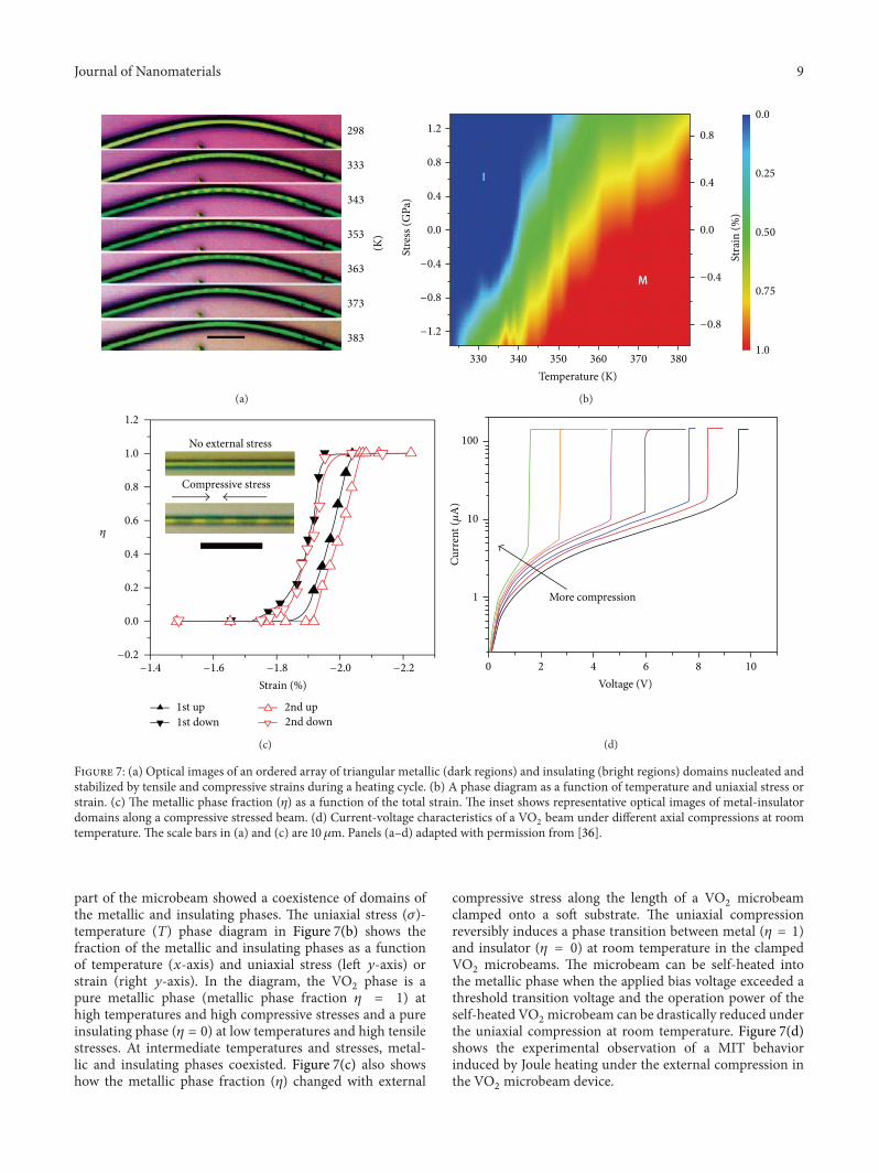
microbeams were nucleated and manipulated by tuning thestrain over a wide range of values, as shown in Figure 7.
Figure 7(a) shows the evolution of domains of triangularshape along a bent VO
2microbeam at different temperatures.
The bent microbeam was in an insulating phase at roomtemperature and periodic triangular domains of the metallicphase started to nucleate at the inner edge of the bentregion (compressive strain) at elevated temperatures. At atemperature near 341 K, the straight part of the microbeamtransformed abruptly to the metallic phase, whereas the bent

8 Journal of Nanomaterials
92888480767268646054494434
Tem
pera
ture
(∘C)
27.2
27.4
27.6
27.8
28.0
28.2
28.4
39.4
39.6
39.8
40.0
40.2
2𝜃 (deg.)
(110)R
(110)R
(200)R
(201)M2(201)M2
(002)M2
(201)M2
(011)M1
(020)M1
High
Low54∘C34∘C 68∘C
34∘C
68∘C64∘C
84∘C80∘C
(a)
Inte
nsity
(a.u
.)In
tens
ity (a
.u.)
Inte
nsity
200 400 600 800 1000
26.8
27.2
27.6
28.0
28.4
28.8
(a.u
.)In
tens
ity
(a.u
.)
273
200
150
100
50
20
Tem
pera
ture
(K)
(011)M1
High
Low
Raman shift (cm−1)
M1 M2
M1 M2
R, 339K
M2, 328K
M2, 339K
M1, 298K
M1+ M2, 323K
M1+ M2, 328K
M1+ M2, 323K
M1+ M2, 318K
M1+ M2, 313K
M1+ M2, 298K
M1+ M2, 318K
M1+ M2, 313K
(201)M2
303K
6K
(011)M1
2𝜃 (deg.)
(b)
Figure 6: (a) Temperature dependence of XRD data measured upon heating from VO2nanobeams epitaxially grown on a c-cut sapphire.
(b) Temperature-dependent Raman spectra obtained from a bent VO2nanobeam on a c-cut sapphire substrate (left panel). Temperature
dependence of XRD data from ensembles of the VO2nanobeams, measured during a cooling cycle from 303 to 6K (right panel). Panels (a)
and (b) adapted with permission from [34] and [35], respectively.
Journal of Nanomaterials 9
298
333
343
353
363
373
383
(K)
(a)
1.2
0.8
0.4
0.0
−0.4
−0.8
−1.2
330 340 350 360 370 380Temperature (K)
0.8
0.4
0.0
−0.4
−0.8
Stra
in (%
)
0.0
0.25
0.50
0.75
1.0
Stre
ss (G
Pa)
(b)
1.2
1.0
0.8
0.6
0.4
0.2
0.0
−0.2−1.4 −1.6 −1.8 −2.0 −2.2
Strain (%)
𝜂
No external stress
Compressive stress
1st up1st down
2nd up2nd down
(c)
100
10
1
0 2 4 6 8 10Voltage (V)
Curr
ent (𝜇A
)
More compression
(d)
Figure 7: (a) Optical images of an ordered array of triangular metallic (dark regions) and insulating (bright regions) domains nucleated andstabilized by tensile and compressive strains during a heating cycle. (b) A phase diagram as a function of temperature and uniaxial stress orstrain. (c) The metallic phase fraction (𝜂) as a function of the total strain. The inset shows representative optical images of metal-insulatordomains along a compressive stressed beam. (d) Current-voltage characteristics of a VO
2beam under different axial compressions at room
temperature. The scale bars in (a) and (c) are 10 𝜇m. Panels (a–d) adapted with permission from [36].
part of the microbeam showed a coexistence of domains ofthe metallic and insulating phases. The uniaxial stress (𝜎)-temperature (T) phase diagram in Figure 7(b) shows thefraction of the metallic and insulating phases as a functionof temperature (𝑥-axis) and uniaxial stress (left 𝑦-axis) orstrain (right 𝑦-axis). In the diagram, the VO
2phase is a
pure metallic phase (metallic phase fraction 𝜂 = 1) athigh temperatures and high compressive stresses and a pureinsulating phase (𝜂 = 0) at low temperatures and high tensilestresses. At intermediate temperatures and stresses, metal-lic and insulating phases coexisted. Figure 7(c) also showshow the metallic phase fraction (𝜂) changed with external
compressive stress along the length of a VO2microbeam
clamped onto a soft substrate. The uniaxial compressionreversibly induces a phase transition between metal (𝜂 = 1)and insulator (𝜂 = 0) at room temperature in the clampedVO2microbeams. The microbeam can be self-heated into
the metallic phase when the applied bias voltage exceeded athreshold transition voltage and the operation power of theself-heated VO
2microbeam can be drastically reduced under
the uniaxial compression at room temperature. Figure 7(d)shows the experimental observation of a MIT behaviorinduced by Joule heating under the external compression inthe VO
2microbeam device.

10 Journal of Nanomaterials
Ram
an in
tens
ity (a
.u.)
Triclinic
Incr
easin
g te
nsile
stra
inM1
M2
𝜔0𝜔V1𝜔V2
200 400 600 800Raman shift (cm−1)
(a)
2.5
2
1.5
1
0.5
0
295 300 305 310 315 320 340Temperature (K)
Relat
ive s
trai
n (%
)
650
645
640
635
630
625
620
615
𝜔0
peak
pos
ition
(cm
−1)
(b)
Figure 8: (a) Raman spectra of a VO2microcrystal showing the tensile strain-dependent evolution of structural phase transitions at room
temperature. (b) A Raman frequency map of strain-temperature phase diagram of the insulating phases of the VO2microcrystal represented
via the 𝜔0phonon frequency shift. Panels (a) and (b) adapted with permission from [37].
To investigate the influence of external stress on crys-tallographic phase transition behavior in VO
2microcrystals,
Atkin et al. [37] employed Raman spectroscopy, which is afacile, rapid, and nondestructive tool for studying the phasetransition properties of individual nano/microstructures.Theauthors demonstrated that, with increasing tensile strain, anM1–T–M2 structural phase transition occurs at temperaturesbelow approximately 305K over a wide range of strain valuesin an individual, homogeneous VO
2microbeam subjected
to external uniaxial strain, as shown in Figures 8(a) and8(b). Figure 8(a) shows Raman spectra of a VO
2microcrystal
showing the evolution in phononmodes with increasing ten-sile strain at room temperature. From these Raman spectra,a Raman frequency map is presented based on the spectralposition of 𝜔
0as a fingerprint for the three different phases
(M1, T, and M2 phases) (Figure 8(b)).
4.4. Influence of Stoichiometry and/or Defects on MIT. TheMIT properties of VO
2are significantly affected by stoi-
chiometry and/or defects due to the fact that vanadium canexist in multiple valence states such as V3+, V4+, and V5+ [38,39, 52–55]. Recently, Zhang and coworkers [38] investigatedthe influence of stoichiometry on the structural phase tran-sition in suspended single-crystalline VO
2nanobeams and
established a pseudo-T-𝛿 phase diagram with dimensions oftemperature and stoichiometry, as shown in Figure 9(a). Theauthors also demonstrated that the annealing of nanobeamsunder vacuum conditions stabilized the rutile phase totemperatures as low as 103K due to the fact that oxygendeficiency contributed to the enhancement of conductivity,providing direct evidence of substantial electron doping inVO2nanobeams (Figure 9(b)). Most recently, Hong et al.
[39] demonstrated a morphotropic phase transformation,which is the phase transition due to the compositionalvariation, in single-crystalline VO
2nanobeams caused by
thermal reduction in a high-pressure hydrogen gas, lead-ing to the stabilization of metallic phases. The authorsshowed that hydrogen significantly reduced oxygen in thenanobeams with characteristic nonlinear reduction kineticswhich depend on the annealing time [39]. Figures 9(c) and9(d) show that the work function and the electrical resistanceof the reduced VO
2nanobeams follow a similar trend to
the compositional variation due to the oxygen deficiencyand related defects. These results imply that the structuralproperties and the electrical resistivity of VO
2nanobeams
are closely correlated with the compositional stoichiometryand/or defects in the nanobeam.
5. Applications
VO2has attracted considerable attention because of a vari-
ety of potential applications based on abrupt reversiblephase transitions at ultrafast timescales in which the phasetransition can be triggered by external perturbations, suchas thermal, electrical, or optical perturbations as well asstrain [1]. Recently, several efforts have been devoted to thedemonstration of potential devices utilizing MITs in VO
2
nanostructures, such as gas sensors, strain sensors, electricalswitches, a thermal memory, and electrical memory devices[40–44, 56, 57].
For example, Strelcov et al. [40] demonstrated a novelgas sensing concept based on suspended VO
2nanowires,
as shown in Figure 10(a), in which the transition propertiesof nanowires strongly depend on the changes in molecular

Journal of Nanomaterials 11
𝛿 VO2−𝛿
340
330
320
310
30050 30 20 10 5 0
T(K
)
R
M1
M2
T
Annealing time (s)
(a)
107
106
105
104
103100 200 300 400
T (K)
R (Ω
)
(b)
1.4
1.2
1.0
0.8
0.6
0.4
00 5 10 15 20 25 30
Reduction time (min)
V/O
ratio
5.4
5.3
5.2
5.1
5.0
4.9
Wor
k fu
nctio
n (Φ
, eV
)
VOx
(c)
0 5 10 15 20 25 30Reduction time (min)
1010
108
106
104
102
Resis
tanc
e (Ω
)
Resistance (Ω)
10
8
6
4
2Num
ber o
f dev
ice
103 105 107 109
As-grown VO230min-r-VO2
5min-r-VO2
1min-r-VO2
VOx
(d)
Figure 9: (a) Structural phase maps (temperature versus annealing time). The shaded background demarcates a pseudo-T-𝛿 phase diagramfor VO
2−𝛿. Confocal reflectivity at a 532 nm laser source. The brighter (darker) regions correspond to the insulating (metallic) phase (upper
image). (b) Resistance versus temperature for as-grown (red) and reduced (green) nanobeams. (c) Change in vanadium (V)/oxygen (O)compositional ratio as a function of reduction time and their corresponding work functions extracted from ultraviolet photoemissionspectroscopy measurements. (d) Electrical resistance as a function of the reduction time for the as-grown and reduced VO
2nanobeams.
The inset shows statistical data of the electrical resistance at room temperature for as-grown VO2and reduced VO
2nanobeams for 1, 5, and
30min at approximately 400∘C under the exposure to hydrogen gas. Panels (a-b) and (c-d) adapted with permission from [38] and [39],respectively.
composition, pressure, and temperature of the ambient gasenvironment. Hu et al. [41] fabricated a flexible strain sensorand a single domain electrical switch based on a VO
2
nanobeam. Figure 10(b) shows the change of the current (I)-voltage (V) behavior solely dependent on the loading strains(compressive and tensile strains) in which the different typesof strain lead to the distinct response from the phase transi-tion between M1 and M2 phases. Hu et al. [42] also showedthat the self-heated VO
2nanobeam under the application of
a bias voltage that exceeds a threshold transition voltage canbe easily switched based on a single domain transition bystretching or compressing the substrate. Figure 10(c) showsa single domain switch based on phase transitions inducedby the coupling of self-heating and external strain in a VO
2
nanobeam.
In addition to the sensor and switching device appli-cations, Xie et al. [43] demonstrated a solid-state thermalmemory that can store and retain thermal informationwith high/low (HI/LO) temperature states, as shown inFigure 11(a). In Figure 11(a), HI/LO temperature states ofrepeatedWrite HI-Read-Write LO-Read cycles using heatingand cooling pulses show the switching performance andrepeatability of the thermal memory. Bae et al. [44] alsoreported a two-terminal memory device based on single VO
2
nanowires that were synthesized by a hydrothermal method,followed by thermal annealing process to form a monoclinicphase (Figure 11(b)). As shown in Figure 11(b), the MITinduced by the Joule heating and the hysteresis behavior leadsto the nonlinear R-V characteristic and eventually enablesthe switchable resistance to be maintained, resulting from

12 Journal of Nanomaterials
V
I
PG
PL
VO2SiO2
10−4
10−5
4 6 8 10Bias (V)
Curr
ent (
A) Pressure
VO2NW
MIT
V+MIT
(a)
20
16
12
8
4
00.0 0.2 0.4 0.6 0.8 1.0 1.2
V (V)
I(n
A)
Compressive strain Tensile strain∼−0.05%∼−0.1%∼−0.15%
∼−0.2%∼−0.25%
∼0.05%∼0.1%∼0.15%
∼0.2%∼0.25%
Originalstatue
50
40
30
20
10
0
0 20 40 60 80 100 120
Tensile Tensile
Original Original
CompressiveI
(nA
)
t (s)
(b)
PDMS
Fixed strain
1E − 3
1E − 4
1E − 5
1E − 6
1E − 7
Stretch ReleaseDC voltage 9.5V
0 20 40 60 80 100 120 140 160Time (s)
Curr
ent (
A)
(c)
Figure 10: Representative devices utilizing MIT in quasi-1D VO2nanostructures. (a)The design and principle of operation of VO
2nanowire
MIT gas sensor (left panel). 𝑃G and 𝑃L indicate heat fluxes dissipating into the gas environment and metal contacts, respectively. Current(I)-bias voltage (V) curves of a self-heated nanowire at different gas pressures showing transition voltages (forward direction) (right panel).(b) I-V curves under different tensile and compressive strains (left panel) and their corresponding response to the strain switch (right panel).(c) Schematic illustration of two-terminal nanobeam device placed on Kapton (left panel). Electrical switch with the strain change based onsingle domain at DC voltage of 9.5 V (right panel). Panels (a), (b), and (c) adapted with permission from [40, 41] and [42], respectively.

Journal of Nanomaterials 13
Tbase
Tin Tout
BiasV
332
328
324
320
316
0 25 50 75 100 125 150Cycle
T out
(K)
440
400
360
320
340
320
300
T out
(K)
T in
(K)
LO LO LO
HI HI HI
Read Read Read Read Read Read
Write HI Write LO Write HI Write HIHigh
Low
Write LO
0 1 2 3 4 5 6 7 8 9 10 11Time (s)
(a)
1011
109
107
Resis
tanc
e (Ω
)
0 1 2 3 4Time (min)
543210
Volta
ge (V
)
1012
1010
108
106
Resis
tanc
e (Ω
)
Voltage (V)0.0 0.2 0.4
VO2(M)
VO2(R)
(I)
(I)(II)
(III)
(IV)
(II)
(III)
(IV)
Signal VO2 nanowire
(b)
Figure 11: (a) A schematic illustration and a SEM image of a thermal memory device with an individual VO2nanobeam connecting the input
terminal (𝑇in) and output terminal (𝑇out) (upper panels). High/low (HI/LO) temperature states over 150 repeated cycles by using a one-secondheating pulse and a one-second cooling pulse at the input terminal under a voltage bias of 0.04V (lower panel).The inset shows the process ofWrite HI-Read-Write LO-Read over three cycles. (b)The resistance (R)-voltage (V) hysteresis curve (upper left panel). Insets show the crystalstructures of VO
2with a monoclinic phase (VO
2(M)) and a rutile phase (VO
2(R)). A schematic of the memory device based on a single VO
2
nanowire showing the gradual change of metallic/insulating phases inside the nanowire at different points marked in the R-V curve (I, II, III,and IV in the upper right panel). Nonvolatile switching property of a single VO
2nanowire memory device (lower panel). Panels (a) and (b)
adapted with permission from [43] and [44], respectively.
the mixed states of metallic and insulating phases during theMIT of the single VO
2nanowire. The multiple retainable
resistances of the single VO2nanowire when two different
voltage pulses are applied repeatedly show the possibility ofnonvolatile memory device utilizing a MIT behavior.
6. Summary
In this review, we first present the basic crystal andmolecularorbital structures of VO
2in metallic and insulating phases
and then discuss the growth characteristics of single-crystalline quasi-1D VO
2structures in terms of their
morphology, composition, and density, which can be signifi-cantly affected by growth conditions such as temperature, gasflow rate, oxygen partial pressure, precursor deposition rate,
and crystallographic plane of growth substrates. Next, wediscuss the influence of doping, surface stress, external stress,and stoichiometry and/or defects on various aspects of phasetransitions in the quasi-1D VO
2structures. Lastly, we present
snapshots of the research carried out emerging applicationsof quasi-1D VO
2structures such as a gas sensor, a flexible
strain sensor, an electrical switch, a thermal memory, anda nonvolatile electrical memory. We expect that this reviewwill give insights not only into understanding the basicimportant aspects of mechanism and properties of quasi-1DVO2materials but also into developing practical applications
for successful commercialization based on MIT technology.

14 Journal of Nanomaterials
Conflict of Interests
The authors declare that there is no conflict of interestsregarding the publication of this paper.
Acknowledgments
Woong-Ki Hong acknowledges the financial supportfrom the National Research Foundation of Korea (NRF)grant funded by the Korean Government (NRF-2013-R1A1A2009884 and NRF-2014M2B2A4030807). SeungNamCha, Jung Inn Sohn, and Jong Min Kim acknowledgethe support from the International Collaborative EnergyTechnology R&D Program of the Korea Institute of EnergyTechnology Evaluation and Planning (KETEP), grantedfinancial resource from the Ministry of Trade, Industry andEnergy, Republic of Korea (no. 20128510010080).
References
[1] Z. Yang, C. Ko, and S. Ramanathan, “Oxide electronics utilizingultrafast metal-insulator transitions,” Annual Review of Materi-als Research, vol. 41, pp. 337–367, 2011.
[2] J. Jeong,N. Aetukuri, T. Graf, T. D. Schladt,M.G. Samant, and S.S. P. Parkin, “Suppression of metal-insulator transition in VO
2
by electric field-induced oxygen vacancy formation,” Science,vol. 339, no. 6126, pp. 1402–1405, 2013.
[3] J. H. Park, J. M. Coy, T. S. Kasirga et al., “Measurement of asolid-state triple point at themetal-insulator transition in VO
2,”
Nature, vol. 500, no. 7463, pp. 431–434, 2013.[4] T. S. Kasirga, D. Sun, J. H. Park et al., “Photoresponse of a
strongly correlated material determined by scanning photocur-rent microscopy,”Nature Nanotechnology, vol. 7, no. 11, pp. 723–727, 2012.
[5] M. M. Qazilbash, M. Brehm, B.-G. Chae et al., “Mott transitionin VO
2revealed by infrared spectroscopy and nano-imaging,”
Science, vol. 318, no. 5857, pp. 1750–1753, 2007.[6] C. Kubler, H. Ehrke, R. Huber et al., “Coherent struc-
tural dynamics and electronic correlations during an ultrafastinsulator-to-metal phase transition in VO
2,” Physical Review
Letters, vol. 99, no. 11, Article ID 116401, 2007.[7] K. Appavoo and R. F. Haglund Jr., “Detecting nanoscale size
dependence inVO2phase transition using a split-ring resonator
metamaterial,” Nano Letters, vol. 11, no. 3, pp. 1025–1031, 2011.[8] R. Lopez, L. A. Boatner, T. E. Haynes, R. F. Haglund Jr., and L.
C. Feldman, “Switchable reflectivity on silicon from a compositeVO2-SiO2protecting layer,” Applied Physics Letters, vol. 85, no.
8, pp. 1410–1412, 2004.[9] A. A. Bugayev and M. C. Gupta, “Femtosecond holographic
interferometry for studies of semiconductor ablation usingvanadium dioxide film,” Optics Letters, vol. 28, no. 16, pp. 1463–1465, 2003.
[10] A. Cavalleri, C. Toth, C. W. Siders et al., “Femtosecond struc-tural dynamics in VO
2during an ultrafast solid-solid phase
transition,” Physical Review Letters, vol. 87, Article ID 237401,2001.
[11] D. Ruzmetov, G. Gopalakrishnan, J. Deng, V. Narayanamurti,and S. Ramanathan, “Electrical triggering of metal-insulatortransition in nanoscale vanadium oxide junctions,” Journal ofApplied Physics, vol. 106, no. 8, Article ID 083702, 2009.
[12] M. J. Dicken, K. Aydin, I. M. Pryce et al., “Frequency tunablenear-infrared metamaterials based on VO
2phase transition,”
Optics Express, vol. 17, no. 20, pp. 18330–18339, 2009.[13] T. Driscoll, H.-T. Kim, B.-G. Chae, M. Di Ventra, and D. N.
Basov, “Phase-transition driven memristive system,” AppliedPhysics Letters, vol. 95, no. 4, Article ID 043503, 2009.
[14] D. Ruzmetov, G. Gopalakrishnan, C. Ko, V. Narayanamurti, andS. Ramanathan, “Three-terminal field effect devices utilizingthin film vanadium oxide as the channel layer,” Journal ofApplied Physics, vol. 107, no. 11, Article ID 114516, 2010.
[15] Q. Gu, A. Falk, J. Q. Wu, L. Ouyang, and H. Park, “Current-driven phase oscillation and domain-wall propagation inW𝑥v1−𝑥
O2nanobeams,” Nano Letters, vol. 7, no. 2, pp. 363–366,
2007.[16] B.-J. Kim,Y.W. Lee, B.-G.Chae et al., “Temperature dependence
of the first-order metal-insulator transition in VO2and pro-
grammable critical temperature sensor,”Applied Physics Letters,vol. 90, no. 2, Article ID 023515, 2007.
[17] R. M. Briggs, I. M. Pryce, and H. A. Atwater, “Compact siliconphotonic waveguide modulator based on the vanadium dioxidemetal-insulator phase transition,” Optics Express, vol. 18, no. 11,pp. 11192–11201, 2010.
[18] J. Cao, W. Fan, Q. Zhou et al., “Colossal thermal-mechanicalactuation via phase transition in single-crystal VO
2microcan-
tilevers,” Journal of Applied Physics, vol. 108, no. 8, Article ID083538, 2010.
[19] H. Guo, M. I. Khan, C. Cheng et al., “VO2nanowire-based
microthermometer for quantitative evaluation of electron beamheating,” Nature Communications, vol. 5, pp. 1–5, 2014.
[20] C. Cheng, D. Fu, K. Liu et al., “Directly metering light absorp-tion and heat transfer in single nanowires usingmetal-insulatortransition in VO
2,” Advanced Optical Materials, vol. 3, no. 3, pp.
336–341, 2015.[21] S. J. Chang, J. B. Park, G. Lee et al., “In situ probing of doping-
and stress-mediated phase transitions in a single-crystallineVO2nanobeam by spatially resolved Raman spectroscopy,”
Nanoscale, vol. 6, no. 14, pp. 8068–8074, 2014.[22] L. Whittaker, C. J. Patridge, and S. Banerjee, “Microscopic and
nanoscale perspective of the metal-insulator phase transitionsof VO
2: some new twists to an old tale,” Journal of Physical
Chemistry Letters, vol. 2, no. 7, pp. 745–758, 2011.[23] Y. Wu, L. Fan, W. Huang et al., “Depressed transition tempera-
ture ofW𝑥V1−𝑥
O2: mechanistic insights from the X-ray absorp-
tion fine structure (XAFS) spectroscopy,” Physical ChemistryChemical Physics, vol. 16, no. 33, pp. 17705–17714, 2014.
[24] M. H. Kim, B. Lee, S. Lee et al., “Growth of metal oxidenanowires from supercooled liquid nanodroplets,”NanoLetters,vol. 9, no. 12, pp. 4138–4146, 2009.
[25] E. Strelcov, A.V.Davydov,U. Lanke, C.Watts, andA.Kolmakov,“In situmonitoring of the growth, intermediate phase transfor-mations and templating of single crystal VO
2nanowires and
nanoplatelets,” ACS Nano, vol. 5, no. 4, pp. 3373–3384, 2011.[26] I. S. Kim and L. J. Lauhon, “Increased yield and uniformity
of vanadium dioxide nanobeam growth via two-step physicalvapor transport process,”Crystal Growth and Design, vol. 12, no.3, pp. 1383–1387, 2012.
[27] B. S. Guiton, Q. Gu, A. L. Prieto, M. S. Gudiksen, and H.Park, “Single-crystalline vanadium dioxide nanowires withrectangular cross sections,” Journal of the American ChemicalSociety, vol. 127, no. 2, pp. 498–499, 2005.
[28] C. Cheng, H. Guo, A. Amini et al., “Self-assembly and horizon-tal orientation growth of VO
2nanowires,” Scientific Reports, vol.
4, pp. 1–5, 2014.

Journal of Nanomaterials 15
[29] J. I. Sohn, H. J. Joo, A. E. Porter et al., “Direct observation of thestructural component of the metal-insulator phase transitionand growth habits of epitaxially grown VO
2nanowires,” Nano
Letters, vol. 7, no. 6, pp. 1570–1574, 2007.[30] E. Strelcov, A. Tselev, I. Ivanov et al., “Doping-based stabiliza-
tion of the M2 phase in free-standing VO2nanostructures at
room temperature,” Nano Letters, vol. 12, no. 12, pp. 6198–6205,2012.
[31] S. Lee, C. Cheng, H. Guo et al., “Axially engineered metal-insulator phase transition by graded doping VO
2nanowires,”
Journal of the American Chemical Society, vol. 135, no. 12, pp.4850–4855, 2013.
[32] J. Wei, H. Ji, W. Guo, A. H. Nevidomskyy, and D. Natelson,“Hydrogen stabilization ofmetallic vanadium dioxide in single-crystal nanobeams,” Nature Nanotechnology, vol. 7, no. 6, pp.357–362, 2012.
[33] J.Wu,Q.Gu, B. S.Guiton,N. P. de Leon, L.Ouyang, andH. Park,“Strain-induced self organization ofmetal-insulator domains insingle-crystalline VO
2nanobeams,” Nano Letters, vol. 6, no. 10,
pp. 2313–2317, 2006.[34] J. I. Sohn, H. J. Joo, D. Ahn et al., “Surface-stress-induced Mott
transition and nature of associated spatial phase transition insingle crystalline VO
2nanowires,” Nano Letters, vol. 9, no. 10,
pp. 3392–3397, 2009.[35] J. I. Sohn, H. J. Joo, K. S. Kim et al., “Stress-induced domain
dynamics and phase transitions in epitaxially grown VO2
nanowires,” Nanotechnology, vol. 23, no. 20, Article ID 205707,2012.
[36] J. Cao, E. Ertekin, V. Srinivasan et al., “Strain engineering andone-dimensional organization of metal–insulator domains insingle-crystal vanadium dioxide beams,” Nature Nanotechnol-ogy, vol. 4, no. 11, pp. 732–737, 2009.
[37] J. M. Atkin, S. Berweger, E. K. Chavez et al., “Strain andtemperature dependence of the insulating phases of VO
2near
the metal-insulator transition,” Physical Review B—CondensedMatter and Materials Physics, vol. 85, no. 2, Article ID 020101,2012.
[38] S. Zhang, I. S. Kim, and L. J. Lauhon, “Stoichiometry engineer-ing of monoclinic to rutile phase transition in suspended singlecrystalline vanadium dioxide nanobeams,”Nano Letters, vol. 11,no. 4, pp. 1443–1447, 2011.
[39] W.-K. Hong, J. B. Park, J. Yoon et al., “Hydrogen-induced mor-photropic phase transformation of single-crystalline vanadiumdioxide nanobeams,” Nano Letters, vol. 13, no. 4, pp. 1822–1828,2013.
[40] E. Strelcov, Y. Lilach, and A. Kolmakov, “Gas sensor based onmetal-insulator transition in VO
2nanowire thermistor,” Nano
Letters, vol. 9, no. 6, pp. 2322–2326, 2009.[41] B. Hu, Y. Ding, W. Chen et al., “External-strain induced insu-
lating phase transition in VO2nanobeam and its application as
flexible strain sensor,” Advanced Materials, vol. 22, no. 45, pp.5134–5139, 2010.
[42] B. Hu, Y. Zhang, W. Chen, C. Xu, and Z. L. Wang, “Self-heatingand external strain coupling induced phase transition of VO
2
nanobeam as single domain switch,” Advanced Materials, vol.23, no. 31, pp. 3536–3541, 2011.
[43] R. Xie, C. T. Bui, B. Varghese et al., “An electrically tunedsolid-state thermalmemory based onmetal-insulator transitionof single-crystalline VO
2nanobeams,” Advanced Functional
Materials, vol. 21, no. 9, pp. 1602–1607, 2011.[44] S.-H. Bae, S. Lee, H. Koo et al., “The memristive properties of a
single VO2nanowire with switching controlled by self-heating,”
Advanced Materials, vol. 25, no. 36, pp. 5098–5103, 2013.
[45] J. Cao, Y. Gu, W. Fan et al., “Extended mapping and explorationof the vanadium dioxide stress-temperature phase diagram,”Nano Letters, vol. 10, no. 7, pp. 2667–2673, 2010.
[46] S. Zhang, J. Y. Chou, and L. J. Lauhon, “Direct correlation ofstructural domain formation with themetal insulator transitionin a VO
2nanobeam,”Nano Letters, vol. 9, no. 12, pp. 4527–4532,
2009.[47] A. C. Jones, S. Berweger, J. Wei, D. Cobden, and M. B.
Raschke, “Nano-optical investigations of the metal-insulatorphase behavior of individual VO
2microcrystals,” Nano Letters,
vol. 10, no. 5, pp. 1574–1581, 2010.[48] N. B. Aetukuri, A. X. Gray, M. Drouard et al., “Control of the
metal-insulator transition in vanadium dioxide by modifyingorbital occupancy,” Nature Physics, vol. 9, no. 10, pp. 661–666,2013.
[49] C. Miller, M. Triplett, J. Lammatao et al., “Unusually long freecarrier lifetime and metal-insulator band offset in vanadiumdioxide,”Physical ReviewB, vol. 85, no. 8, Article ID 085111, 2012.
[50] Y. Cheng, T. Zhang, Y. Cai, K. M. Ho, K. K. Fung, and N.Wang,“Structure and metal-to-insulator transition of VO
2nanowires
grown on sapphire substrates,” European Journal of InorganicChemistry, vol. 2010, no. 27, pp. 4332–4338, 2010.
[51] H. Guo, K. Wang, Y. Deng et al., “Nanomechanical actua-tion from phase transitions in individual VO
2micro-beams,”
Applied Physics Letters, vol. 102, no. 23, Article ID 231909, 2013.[52] C. H. Griffiths and H. K. Eastwood, “Influence of stoichiometry
on the metal-semiconductor transition in vanadium dioxide,”Journal of Applied Physics, vol. 45, no. 5, pp. 2201–2206, 1974.
[53] C. Ko, Z. Yang, and S. Ramanathan, “Work function of vana-dium dioxide thin films across the metal-insulator transitionand the role of surface nonstoichiometry,” ACS Applied Mate-rials and Interfaces, vol. 3, no. 9, pp. 3396–3401, 2011.
[54] E.Hryha, E. Rutqvist, and L.Nyborg, “Stoichiometric vanadiumoxides studied by XPS,” Surface and Interface Analysis, vol. 44,no. 8, pp. 1022–1025, 2012.
[55] C. Clavero, J. L. Slack, and A. Anders, “Size and composition-controlled fabrication of thermochromicmetal oxide nanocrys-tals,” Journal of Physics D: Applied Physics, vol. 46, no. 36, ArticleID 362001, 2013.
[56] A. Simo, B. Mwakikunga, B. T. Sone, B. Julies, R. Madjoe, andM. Maaza, “VO
2nanostructures based chemiresistors for low
power energy consumption hydrogen sensing,” InternationalJournal of Hydrogen Energy, vol. 39, no. 15, pp. 8147–8157, 2014.
[57] K. J. Choi and H. W. Jang, “One-dimensional oxide nanostruc-tures as gas-sensing materials: review and issues,” Sensors, vol.10, no. 4, pp. 4083–4099, 2010.

Submit your manuscripts athttp://www.hindawi.com
ScientificaHindawi Publishing Corporationhttp://www.hindawi.com Volume 2014
CorrosionInternational Journal of
Hindawi Publishing Corporationhttp://www.hindawi.com Volume 2014
Polymer ScienceInternational Journal of
Hindawi Publishing Corporationhttp://www.hindawi.com Volume 2014
Hindawi Publishing Corporationhttp://www.hindawi.com Volume 2014
CeramicsJournal of
Hindawi Publishing Corporationhttp://www.hindawi.com Volume 2014
CompositesJournal of
NanoparticlesJournal of
Hindawi Publishing Corporationhttp://www.hindawi.com Volume 2014
Hindawi Publishing Corporationhttp://www.hindawi.com Volume 2014
International Journal of
Biomaterials
Hindawi Publishing Corporationhttp://www.hindawi.com Volume 2014
NanoscienceJournal of
TextilesHindawi Publishing Corporation http://www.hindawi.com Volume 2014
Journal of
NanotechnologyHindawi Publishing Corporationhttp://www.hindawi.com Volume 2014
Journal of
CrystallographyJournal of
Hindawi Publishing Corporationhttp://www.hindawi.com Volume 2014
The Scientific World JournalHindawi Publishing Corporation http://www.hindawi.com Volume 2014
Hindawi Publishing Corporationhttp://www.hindawi.com Volume 2014
CoatingsJournal of
Advances in
Materials Science and EngineeringHindawi Publishing Corporationhttp://www.hindawi.com Volume 2014
Smart Materials Research
Hindawi Publishing Corporationhttp://www.hindawi.com Volume 2014
Hindawi Publishing Corporationhttp://www.hindawi.com Volume 2014
MetallurgyJournal of
Hindawi Publishing Corporationhttp://www.hindawi.com Volume 2014
BioMed Research International
MaterialsJournal of
Hindawi Publishing Corporationhttp://www.hindawi.com Volume 2014
Nano
materials
Hindawi Publishing Corporationhttp://www.hindawi.com Volume 2014
Journal ofNanomaterials
Related Documents