Research Article Modeling, Design, and Fabrication of Self-Doping Si 1−x Ge x /Si Multiquantum Well Material for Infrared Sensing Bo Jiang, 1 Dandan Gu, 2 Yulong Zhang, 2 Yan Su, 1 Yong He, 1 and Tao Dong 3 1 Mechanical Engineering School, Nanjing University of Science and Technology, Nanjing, China 2 Pen-Tung Sah Institute of Micro-Nano Science and Technology, Xiamen University, Xiamen, China 3 Department of Micro and Nano Systems Technology (IMST), Faculty of Technology and Maritime Sciences, Buskerud and Vestfold University College, Raveien 205, 3184 Borre, Norway Correspondence should be addressed to Dandan Gu; [email protected], Yulong Zhang; [email protected], and Tao Dong; [email protected] Received 17 September 2015; Accepted 22 October 2015 Academic Editor: Wei Cao Copyright © 2016 Bo Jiang et al. is is an open access article distributed under the Creative Commons Attribution License, which permits unrestricted use, distribution, and reproduction in any medium, provided the original work is properly cited. e paper presents the study of band distributions and thermoelectric properties of self-doping Si 1−x Ge x /Si multiquantum well material for infrared detection. e simulations of different structures (including boron doping, germanium concentrations, and SiGe layer thickness) have been conducted. e critical thickness of SiGe layer grown on silicon substrate has also been illustrated in the paper. e self-doping Si 1−x Ge x /Si multiquantum well material was epitaxially grown on SOI substrate with reduced pressure chemical vapor deposition. Each layer of the material is clear in the SEM. e - characterizations and temperature resistance coefficient (TCR) tests were also performed to show the thermoelectric properties. e TCR was about −3.7%/K at room temperature in the experiments, which is competitive with the other thermistor materials. e material is a low noise material, whose root mean square noise is 1.89 mV in the experiments. 1. Introduction Bolometer, one of uncooled infrared detectors, has been widely developed since 1992, when the “bridge structure” was reported by Honeywell. Bolometers are thermal infrared sensors that absorb electromagnetic radiation (8–14 m) and thus increase their temperature [1–4]. e materials with high TCR (temperature resistance coefficient) are preferred to increase the sensitivity. Vanadium oxide and amorphous silicon are the most successful materials and occupy the major commercial market share [5]. e bolometer pixel size is developed to 17 m, while the resolution is to 1920 × 1080 or even more [6, 7]. As a result of technical development, the next generation of bolometer should be combined with standard CMOS based integrated circuits to decrease the cost. However, vanadium is one of deep level pollution elements for the IC process [8, 9]. e special process line should be provided for vanadium oxide manufacture, which would be expensive in bolometer development. As a result, more and more researches have focused on the novel material with high TCR, which can also be compatible with IC industry. Various semiconductor materials are the most suitable materials among them. Si 1− Ge /Si multiquantum wells (MQWs) have been proposed recently as a new thermistor material [10, 11]. ough the material has shown achieved good performance, it leads to some difficulties because of the practical growth process. With the rising complexity in this process, the cost and difficulties also increase to maintain the lattice quality. In our previous works, the high TCR material with self- doping Si 1− Ge /Si MQWs films was presented to solve the problems. e material has a thin buffer layer, where a proportion of boron atom diffusion is allowed [12]. is structure simplifies the process and can also promise a high lattice quality through epitaxial growth processes, such as the reduced pressure chemical vapor deposition (RPCVD) and molecular beam epitaxy (MBE). e works subsequently focus on the relationships between the energy bands mod- eling and doping distributions. e epitaxial processes were optimized and more characterizations about material noise were taken. Hindawi Publishing Corporation Journal of Sensors Volume 2016, Article ID 6584650, 7 pages http://dx.doi.org/10.1155/2016/6584650

Welcome message from author
This document is posted to help you gain knowledge. Please leave a comment to let me know what you think about it! Share it to your friends and learn new things together.
Transcript

Research ArticleModeling, Design, and Fabrication of Self-Doping Si1−xGex/SiMultiquantum Well Material for Infrared Sensing
Bo Jiang,1 Dandan Gu,2 Yulong Zhang,2 Yan Su,1 Yong He,1 and Tao Dong3
1Mechanical Engineering School, Nanjing University of Science and Technology, Nanjing, China2Pen-Tung Sah Institute of Micro-Nano Science and Technology, Xiamen University, Xiamen, China3Department of Micro and Nano Systems Technology (IMST), Faculty of Technology and Maritime Sciences,Buskerud and Vestfold University College, Raveien 205, 3184 Borre, Norway
Correspondence should be addressed to Dandan Gu; [email protected], Yulong Zhang; [email protected],and Tao Dong; [email protected]
Received 17 September 2015; Accepted 22 October 2015
Academic Editor: Wei Cao
Copyright © 2016 Bo Jiang et al.This is an open access article distributed under the Creative Commons Attribution License, whichpermits unrestricted use, distribution, and reproduction in any medium, provided the original work is properly cited.
The paper presents the study of band distributions and thermoelectric properties of self-doping Si1−xGex/Si multiquantum well
material for infrared detection. The simulations of different structures (including boron doping, germanium concentrations, andSiGe layer thickness) have been conducted. The critical thickness of SiGe layer grown on silicon substrate has also been illustratedin the paper. The self-doping Si
1−xGex/Si multiquantum well material was epitaxially grown on SOI substrate with reducedpressure chemical vapor deposition. Each layer of the material is clear in the SEM. The 𝐼-𝑉 characterizations and temperatureresistance coefficient (TCR) tests were also performed to show the thermoelectric properties.The TCR was about −3.7%/K at roomtemperature in the experiments, which is competitive with the other thermistor materials. The material is a low noise material,whose root mean square noise is 1.89mV in the experiments.
1. Introduction
Bolometer, one of uncooled infrared detectors, has beenwidely developed since 1992, when the “bridge structure”was reported by Honeywell. Bolometers are thermal infraredsensors that absorb electromagnetic radiation (8–14 𝜇m) andthus increase their temperature [1–4]. The materials withhigh TCR (temperature resistance coefficient) are preferredto increase the sensitivity. Vanadium oxide and amorphoussilicon are the most successful materials and occupy themajor commercial market share [5]. The bolometer pixel sizeis developed to 17 𝜇m, while the resolution is to 1920 × 1080or even more [6, 7]. As a result of technical development,the next generation of bolometer should be combined withstandardCMOSbased integrated circuits to decrease the cost.However, vanadium is one of deep level pollution elementsfor the IC process [8, 9]. The special process line should beprovided for vanadium oxide manufacture, which would beexpensive in bolometer development. As a result, more andmore researches have focused on the novelmaterial with high
TCR, which can also be compatible with IC industry. Varioussemiconductor materials are the most suitable materialsamong them. Si
1−𝑥Ge𝑥/Si multiquantumwells (MQWs) have
been proposed recently as a new thermistor material [10, 11].Though the material has shown achieved good performance,it leads to some difficulties because of the practical growthprocess. With the rising complexity in this process, the costand difficulties also increase to maintain the lattice quality.
In our previous works, the high TCR material with self-doping Si
1−𝑥Ge𝑥/Si MQWs films was presented to solve
the problems. The material has a thin buffer layer, wherea proportion of boron atom diffusion is allowed [12]. Thisstructure simplifies the process and can also promise a highlattice quality through epitaxial growth processes, such asthe reduced pressure chemical vapor deposition (RPCVD)and molecular beam epitaxy (MBE).The works subsequentlyfocus on the relationships between the energy bands mod-eling and doping distributions. The epitaxial processes wereoptimized and more characterizations about material noisewere taken.
Hindawi Publishing CorporationJournal of SensorsVolume 2016, Article ID 6584650, 7 pageshttp://dx.doi.org/10.1155/2016/6584650

2 Journal of Sensors
In the paper, the modeling of quantum well structuresis introduced firstly. The band distributions of MQWs withdifferent structures are calculated and illustrated in thepart. The section also presents the epitaxial processes andcharacterization experiments. The SEM and electrical testswere conducted and shown in Section 3. The results showthat the lattice of self-doping Si
1−𝑥Ge𝑥/Si multiquantum well
material has good quality and the TCR is −3.7%/K, which ishigh compared with other material in the reports [13].
2. Energy Bands Modeling and Design
The resistance is temperature dependent for semiconductor.There is a close relationship between energy bands distribu-tions and thermoelectric properties.The study of energy bansmodeling is helpful to determine theMQWs structure. For𝑝-type semiconductor, the carriers concentration follows [14]
𝑝
0= 𝑁V𝑒
−(𝐸𝑓−𝐸V)/𝑘𝑇,
(1)
where 𝐸𝑓is Fermi level, 𝐸V is valence band, 𝑘 is Boltzmann’s
constant, 𝑇 is temperature, and effective carriers concentra-tion,𝑁V, is followed by
𝑁V = 2(2𝜋𝑚
𝑝× 𝑘𝑇
ℎ
2)
3/2
,
(2)
where𝑚𝑝is effective mass and ℎ is Planck’s constant.
Equation (1) illustrates the relationship between 𝑝-typesemiconductor resistance and the temperature. The materialTCR is defined as
𝛼 =
𝜕𝑅/𝜕𝑇
𝑅
,
(3)
where 𝑅 is the resistance of the material, which is inverselyproportional to the hole concentration, 𝑝
0, for the 𝑝-doped
semiconductor. Equation (4) can be derived by (1) to (3) as
𝛼 = −
1
𝑘𝑇
2(
3
2
𝑘𝑇 + 𝐸
𝑓− 𝐸V) . (4)
Equation (4) indicates the critical principle between theenergy bands and the electrical properties of𝑝-type semicon-ductors. As shown in (4), TCR increases with the rise of thedistance from the Fermi level to the valence band.
The structures of Si/SiGemultiquantumwells and the cor-responding valence energy bands are illustrated in Figure 1.The valence bands are split to heavy hole (HH), light hole(LH), and spin-split-off (SO) bands, where each band hastwo states, that is, spin-up and spin-down [15]. For cooledinfrared detector, the photons transit fromHH to LHor otherenergy levels, where the energy differences are consistentwiththe wavelength of infrared incidence. The process is a kindof photon-electrical effects, which needs pretty low workingtemperatures (e.g., 77 K) to depress the thermal noises [16].For uncooled infrared detector, there is no effective photon-electrical process for the corresponding infrared incidence.The studies focus on increasing the energy gap between Fermilevel and the valence band.
Material structures Energy bands
Si
Si
Si
Si
Si1−xGex
Si1−xGex
Si1−xGex
EfEHH ELH
ESO
E�
Figure 1: The structures of Si/SiGe multiquantum wells and thecorresponding valence energy bands.
The valence barrier (silicon layer) is about 30 nm. It isbig enough and there are few influences for quantum wellsadjacently. Three points should be taken into account inSi/SiGemultiquantumwells design, which are listed as below:
(1) Boron doping distributions in quantum well struc-tures.
(2) Quantum well, SiGe layer thickness of the material.
(3) Germanium concentration in SiGe layer.
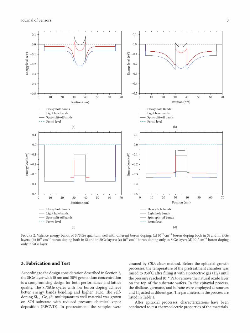
The simulations results of valence energy bands withdifferent boron doping distributions are carried out with thesoftware NextNano3, and the results were shown as Figure 2.In the simulation, the thickness and doping concentration(for both boron and germanium) of barriers and quantumwell were defined. The simulation was conducted with nobias voltage. For self-doping structures, the boron dopingdistributions are similar in both Si layers and SiGe layers.Thebands are curved due to high boron doping. The structureswith lower doping (1018 cm−3) obtain bigger differencesbetween Fermi level and the valence band. The energy gapin Figure 2(a) is about 0.18 eV and the value is about 0.25 eVin Figure 2(b). The high boron doping only in SiGe layerachieves better performance. The energy gap is 3.6 eV inFigure 2(c) with 1019 cm−3 boron doping only in Si layer.However, it is impossible to achieve because the diffusion willhappen in epitaxial process (process temperature ismore than600∘C). The energy gap decreases when the boron dopingdecreases in SiGe layer as shown in Figure 2(d).
The thickness and the Ge concentration in SiGe layer areanother two critical parameters to enhance TCR. The TCRincreases with the increasing of Ge concentration and SiGelayer thickness as shown in Figure 3(a). High germaniumachieves high TCR effectively. However, the lattice mismatchbetween silicon and germanium leads to strain or evendislocation or defects during epitaxial process. The epitaxialSiGe layer should be thinner than the critical thicknesswith corresponding Ge concentration on silicon substrate.The relationship between germanium concentration and thecritical thickness is illustrated in Figure 3(b).
Journal of Sensors 3
0 10 20 30 40 50 60 70−0.5
−0.4
−0.3
−0.2
−0.1
0.0
0.1
Ener
gy le
vel (
eV)
Position (nm)
Heavy hole bands
Spin-split-off bands Light hole bands
Fermi level(a)
0 10 20 30 40 50 60 70−0.5
−0.4
−0.3
−0.2
−0.1
0.0
0.1
Ener
gy le
vel (
eV)
Position (nm)
Heavy hole Bands
Spin-split-off bands Light hole bands
Fermi level(b)
0 10 20 30 40 50 60 70−0.5
−0.4
−0.3
−0.2
−0.1
0.0
0.1
Ener
gy le
vel (
eV)
Position (nm)
Heavy hole bands
Spin-split-off bands Light hole bands
Fermi level(c)
0 10 20 30 40 50 60 70−0.5
−0.4
−0.3
−0.2
−0.1
0.0
0.1
Ener
gy le
vel (
eV)
Position (nm)
Heavy hole bands
Spin-split-off bands Light hole bands
Fermi level(d)
Figure 2: Valence energy bands of Si/SiGe quantum well with different boron doping: (a) 1019 cm−3 boron doping both in Si and in SiGelayers; (b) 1018 cm−3 boron doping both in Si and in SiGe layers; (c) 1019 cm−3 boron doping only in SiGe layer; (d) 1018 cm−3 boron dopingonly in SiGe layer.
3. Fabrication and Test
According to the design consideration described in Section 2,the SiGe layer with 10 nm and 30% germanium concentrationis a compromising design for both performance and latticequality. The Si/SiGe cycles with low boron doping achievebetter energy bands bending and higher TCR. The self-doping Si
1−𝑥Ge𝑥/Si multiquantum well material was grown
on SOI substrate with reduced pressure chemical vapordeposition (RPCVD). In pretreatment, the samples were
cleaned by CRA-clean method. Before the epitaxial growthprocesses, the temperature of the pretreatment chamber wasraised to 950∘C after filling it with a protective gas (H
2) until
the pressure reached 10−2 Pa to remove the natural oxide layeron the top of the substrate wafers. In the epitaxial process,the disilane, germane, and borane were employed as sourcesandH
2acted as diluent gas.The parameters in the process are
listed in Table 1.After epitaxial processes, characterizations have been
conducted to test thermoelectric properties of the materials.

4 Journal of Sensors
The SiGe layer thickness (nm)
TCR
(%/K
)
4 6 8 10 12 14 160.0
0.8
1.6
2.4
3.2
4.0
Ge 35% Ge 30%
Ge 25% Ge 20%
(a)
0.0 0.2 0.4 0.6 0.8 1.01
10
100
Single layerMultiple layers
Germanium concentration in SiGe layer
The c
ritic
al th
ickn
ess o
f SiG
e lay
er (n
m) 1k
(b)
Figure 3: (a) The TCR of the structures with different germanium concentration and well thickness [11]; (b) the critical thicknesses withgermanium concentration of SiGe layer growth on silicon substrate.
Table 1: Epitaxial process parameters of Si/SiGe MQWs with RPCVD.
Steps Temperature (∘C) Sources Flow (sccm) Time Comments1 600 Si
2H6/BH3/H2
6/1/80 30min High boron doping Si, 200 nm2 600 Si
2H6/H2
6/60 9min Buffer layer, 60 nm3 600 Si
2H6/GeH
4/H2
6/2.6/80 100 s Si/SiGe cycles (30 nm/10 nm)4 600 Si
2H6/H2
6/60 4.5min5 600 Si
2H6/BH3/H2
6/1/80 30min High boron doping Si, 200 nm
The test structures were processed and bonded as shown inFigures 4(a) and 4(c). The material was etched with SF
6till
high boron doping Si layer for electrical connection betweentwo pads. The high boron doping silicon layer acted aselectrical connection layer in the test and the current path isshown as illustrated in Figure 4(b). After that, Au wires werebonded on electrode pads to the packaging shell. 𝐼-𝑉 testswere conducted, and the results are shown as Figure 6.
4. Results and Discussion
The SEM of self-doping Si1−𝑥
Ge𝑥/Si multiquantum well
material was shown as Figure 5. The material was grownon SOI substrate. In the figure, SiGe layers, which are only10 nm thick for each layer, are shown clearly.The silicon layerswithout boron doping are 30 nm, which function as barrierlayers in the quantum well structures. Buffer layer is about35 nm and the boron atoms diffused into the multiquantumwell structures in high temperature epitaxial process. Highboron doping layers are about 150 nm as shown in the figure.
The noise tests were conducted and the lower frequencynoise is dominant, such as 1/𝑓noise andDCnoise [17, 18].Thenoise voltage is about 8mV/√Hz in low frequency and lessthan 0.01mV/√Hz in high frequency. The root mean squarenoise is 1.89mV as calculations as shown in Figure 6.
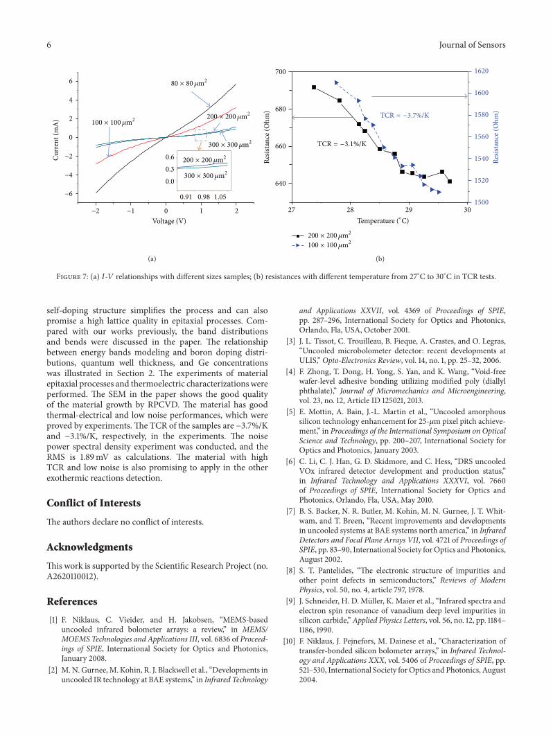
Electrical characterizations have been conducted forthermoelectric properties of the materials after packaging.The 𝐼-𝑉 tests have been performed with different sizedsamples. The voltage was changing from −2V to 2V andthe step is 0.04V for each point. The experiments wereperformed at the room temperature. The results have beenillustrated in Figure 7(a). The resistance decreases whenthe bias voltage rises. It is because the transient joule heatincreases with higher bias voltage. The resistance increaseswith the decreasing of the sample size, which also follows theresistance law for multiquantum well structures.
The relationship between temperature and resistance ofthe samples is shown in Figure 7(b). The experiments wereconducted at room temperature, which is also the workingtemperature for uncooled infrared detector. The samplewith smaller size has better thermal-sensitive characteristicscompared with the larger one as the results. The TCR ofthe samples are −3.7%/K and −3.1%/K, respectively, as thecalculations with (3). It is high compared with other materialin the reports [12].
5. Conclusions
The paper presents the modeling and design of self-dopingSi1−𝑥
Ge𝑥/Si multiquantum well material. The design with

Journal of Sensors 5
Test unit
Electrode pads
High boron doping Si layer
−0.70.92(𝜇
m)
(𝜇m
)
1.2
0.00 0.0
(mm) (mm)
1.33
1.10
0.80
0.50
0.20
−0.10
−0.40
−0.69
(a) (b)
Au bonding wires
`
(c)
Figure 4: (a) The 3D profiler image of test structures after processes; (b) the current path in the 𝐼-𝑉 test experiments; (c) bonding with Auwire in the packaging.
SiGe layers
Si layersBuffer layers
Buffer layers
High boron doping layers
High boron doping layers
Surface of sample
Figure 5: The SEM of self-doping Si1−𝑥
Ge𝑥/Si multiquantum well material.
10−3
10−4
10−5
10−6
Noi
se v
olta
ge (V
/
10−2 10−1 100 101
Frequence (kHz)
Thompson multitaper power spectral density estimate
√H
z)
Figure 6: Noise power spectral density for the material.
6 Journal of Sensors
−2 −1 0 1 2
−6
−4
−2
0
2
4
6
Curr
ent (
mA
)
Voltage (V)
0.91 0.98 1.05
0.00.30.6
100 × 100𝜇m2
80 × 80𝜇m2
200 × 200𝜇m2
300 × 300𝜇m2
200 × 200𝜇m2
300 × 300𝜇m2
(a)
700
680
660
640
Resis
tanc
e (O
hm)
Resis
tanc
e (O
hm)TCR = −3.7%/K
TCR = −3.1%/K
1620
1600
1580
1560
1540
1520
150027 28 29 30
Temperature (∘C)
100 × 100𝜇m2200 × 200𝜇m2
(b)
Figure 7: (a) 𝐼-𝑉 relationships with different sizes samples; (b) resistances with different temperature from 27∘C to 30∘C in TCR tests.
self-doping structure simplifies the process and can alsopromise a high lattice quality in epitaxial processes. Com-pared with our works previously, the band distributionsand bends were discussed in the paper. The relationshipbetween energy bands modeling and boron doping distri-butions, quantum well thickness, and Ge concentrationswas illustrated in Section 2. The experiments of materialepitaxial processes and thermoelectric characterizations wereperformed. The SEM in the paper shows the good qualityof the material growth by RPCVD. The material has goodthermal-electrical and low noise performances, which wereproved by experiments. The TCR of the samples are −3.7%/Kand −3.1%/K, respectively, in the experiments. The noisepower spectral density experiment was conducted, and theRMS is 1.89mV as calculations. The material with highTCR and low noise is also promising to apply in the otherexothermic reactions detection.
Conflict of Interests
The authors declare no conflict of interests.
Acknowledgments
This work is supported by the Scientific Research Project (no.A2620110012).
References
[1] F. Niklaus, C. Vieider, and H. Jakobsen, “MEMS-baseduncooled infrared bolometer arrays: a review,” in MEMS/MOEMS Technologies and Applications III, vol. 6836 of Proceed-ings of SPIE, International Society for Optics and Photonics,January 2008.
[2] M.N. Gurnee,M. Kohin, R. J. Blackwell et al., “Developments inuncooled IR technology at BAE systems,” in Infrared Technology
and Applications XXVII, vol. 4369 of Proceedings of SPIE,pp. 287–296, International Society for Optics and Photonics,Orlando, Fla, USA, October 2001.
[3] J. L. Tissot, C. Trouilleau, B. Fieque, A. Crastes, and O. Legras,“Uncooled microbolometer detector: recent developments atULIS,” Opto-Electronics Review, vol. 14, no. 1, pp. 25–32, 2006.
[4] F. Zhong, T. Dong, H. Yong, S. Yan, and K. Wang, “Void-freewafer-level adhesive bonding utilizing modified poly (diallylphthalate),” Journal of Micromechanics and Microengineering,vol. 23, no. 12, Article ID 125021, 2013.
[5] E. Mottin, A. Bain, J.-L. Martin et al., “Uncooled amorphoussilicon technology enhancement for 25-𝜇m pixel pitch achieve-ment,” in Proceedings of the International Symposium on OpticalScience and Technology, pp. 200–207, International Society forOptics and Photonics, January 2003.
[6] C. Li, C. J. Han, G. D. Skidmore, and C. Hess, “DRS uncooledVOx infrared detector development and production status,”in Infrared Technology and Applications XXXVI, vol. 7660of Proceedings of SPIE, International Society for Optics andPhotonics, Orlando, Fla, USA, May 2010.
[7] B. S. Backer, N. R. Butler, M. Kohin, M. N. Gurnee, J. T. Whit-wam, and T. Breen, “Recent improvements and developmentsin uncooled systems at BAE systems north america,” in InfraredDetectors and Focal Plane Arrays VII, vol. 4721 of Proceedings ofSPIE, pp. 83–90, International Society forOptics and Photonics,August 2002.
[8] S. T. Pantelides, “The electronic structure of impurities andother point defects in semiconductors,” Reviews of ModernPhysics, vol. 50, no. 4, article 797, 1978.
[9] J. Schneider, H. D. Muller, K. Maier et al., “Infrared spectra andelectron spin resonance of vanadium deep level impurities insilicon carbide,” Applied Physics Letters, vol. 56, no. 12, pp. 1184–1186, 1990.
[10] F. Niklaus, J. Pejnefors, M. Dainese et al., “Characterization oftransfer-bonded silicon bolometer arrays,” in Infrared Technol-ogy and Applications XXX, vol. 5406 of Proceedings of SPIE, pp.521–530, International Society forOptics and Photonics, August2004.

Journal of Sensors 7
[11] L. Zhang andT.Dong, “A Si/SiGe quantumwell based biosensorfor direct analysis of exothermic biochemical reaction,” Journalof Micromechanics and Microengineering, vol. 23, no. 4, ArticleID 045011, 2013.
[12] B. Jiang, T. Dong, Y. Su, Y. He, and K. Wang, “Epitaxial growthand characterization of self-doping Si
1−𝑥Ge𝑥/Si multi-quantum
well materials,” Journal of Microelectromechanical Systems, vol.23, no. 1, Article ID 6558494, pp. 213–219, 2014.
[13] J. Y. Andersson, P. Ericsson, H. H. Radamson, S. G. E. Wissmar,andM.Kolahdouz, “SiGe/Si quantum structures as a thermistormaterial for low cost IR microbolometer focal plane arrays,”Solid-State Electronics, vol. 60, no. 1, pp. 100–104, 2011.
[14] S.Wissmar, L. Hoglund, J. Andersson, C. Vieider, S. Savage, andP. Ericsson, “High signal-to-noise ratio quantumwell bolometermaterials,” in Optical Materials in Defence Systems TechnologyIII, vol. 6401 of Proceedings of SPIE, International Society forOptics and Photonics, Stockholm, Sweden, September 2006.
[15] G. Hionis and G. P. Triberis, “Hole subband non-parabolicitiesin strained Si/Si1−𝑥Ge𝑥 quantum wells,” Superlattices andMicrostructures, vol. 24, no. 6, pp. 399–407, 1998.
[16] A. Rogalski, “Quantumwell photoconductors in infrared detec-tor technology,” Journal of Applied Physics, vol. 93, no. 8, pp.4355–4391, 2003.
[17] T. Zhou, T. Dong, Y. Su, and Y. He, “A cmos readout with high-precision and low-temperature-coefficient background currentskimming for infrared focal plane array,” IEEE Transactions onCircuits and Systems for Video Technology, vol. 25, no. 8, pp.1447–1455, 2014.
[18] T. Zhou, T.Dong, Y. Su, andY.He, “High-precision and low-costwireless 16-channel measurement system for multi-layer thinfilm characterization,” Measurement, vol. 46, no. 9, pp. 3600–3611, 2013.

International Journal of
AerospaceEngineeringHindawi Publishing Corporationhttp://www.hindawi.com Volume 2014
RoboticsJournal of
Hindawi Publishing Corporationhttp://www.hindawi.com Volume 2014
Hindawi Publishing Corporationhttp://www.hindawi.com Volume 2014
Active and Passive Electronic Components
Control Scienceand Engineering
Journal of
Hindawi Publishing Corporationhttp://www.hindawi.com Volume 2014
International Journal of
RotatingMachinery
Hindawi Publishing Corporationhttp://www.hindawi.com Volume 2014
Hindawi Publishing Corporation http://www.hindawi.com
Journal ofEngineeringVolume 2014
Submit your manuscripts athttp://www.hindawi.com
VLSI Design
Hindawi Publishing Corporationhttp://www.hindawi.com Volume 2014
Hindawi Publishing Corporationhttp://www.hindawi.com Volume 2014
Shock and Vibration
Hindawi Publishing Corporationhttp://www.hindawi.com Volume 2014
Civil EngineeringAdvances in
Acoustics and VibrationAdvances in
Hindawi Publishing Corporationhttp://www.hindawi.com Volume 2014
Hindawi Publishing Corporationhttp://www.hindawi.com Volume 2014
Electrical and Computer Engineering
Journal of
Advances inOptoElectronics
Hindawi Publishing Corporation http://www.hindawi.com
Volume 2014
The Scientific World JournalHindawi Publishing Corporation http://www.hindawi.com Volume 2014
SensorsJournal of
Hindawi Publishing Corporationhttp://www.hindawi.com Volume 2014
Modelling & Simulation in EngineeringHindawi Publishing Corporation http://www.hindawi.com Volume 2014
Hindawi Publishing Corporationhttp://www.hindawi.com Volume 2014
Chemical EngineeringInternational Journal of Antennas and
Propagation
International Journal of
Hindawi Publishing Corporationhttp://www.hindawi.com Volume 2014
Hindawi Publishing Corporationhttp://www.hindawi.com Volume 2014
Navigation and Observation
International Journal of
Hindawi Publishing Corporationhttp://www.hindawi.com Volume 2014
DistributedSensor Networks
International Journal of
Related Documents


