SiGe-THz devices: Physics and reliability 17 December 2015, Bordeaux Reliability aware circuit design Cristell Maneux University of Bordeaux

Welcome message from author
This document is posted to help you gain knowledge. Please leave a comment to let me know what you think about it! Share it to your friends and learn new things together.
Transcript
SiGe-THz devices: Physics and reliability
17 December 2015, Bordeaux
Reliability aware circuit design Cristell Maneux University of Bordeaux
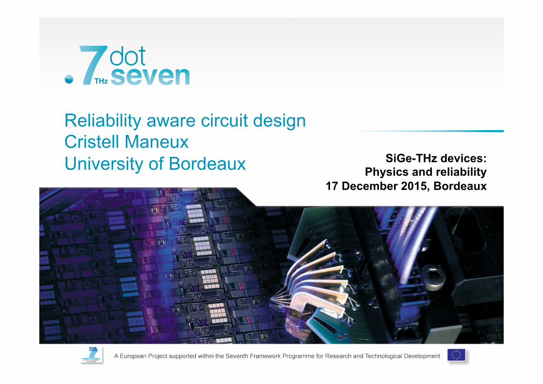
Outline • Context :
• Impact of dimensions shrinking on device operation margins • Impact of device operation margins on the device failure mechanisms
• From device to circuit reliability • Circuit aging simulation : Why ? • Circuit aging simulation : How?
• Conventional way of doing • IMS proposal for circuit aging simulation
• A study case : InP Bipolar Submicron devices for robust design of 112Gb/s optical transport network
• DOTSEVEN SiGe HBT technology • Operation • Aging tests results • Aging laws implementation in HiCUM model • Towards the evaluation of reliability at circuit level
2

SiGe HBT basics : device architecture
Fox et al., ’’Heterojunction bipolar transistor for Half-THz SiGe BiCMOS technology’’, IEEE Electron Device Letters, Vol. 36, N°7, July 2015.
3
WExLE = 0.13x2.69µm2
fT =300GHz fMAX =500GHz JC (peak fT)=17mA/µm2
BVCE0=1.5V

DOTSEVEN SiGe HBTs: Performances
4
Fox et al., ’’Heterojunction bipolar transistor for Half-THz SiGe BiCMOS technology’’, IEEE Electron Device Letters, Vol. 36, N°7, July 2015.
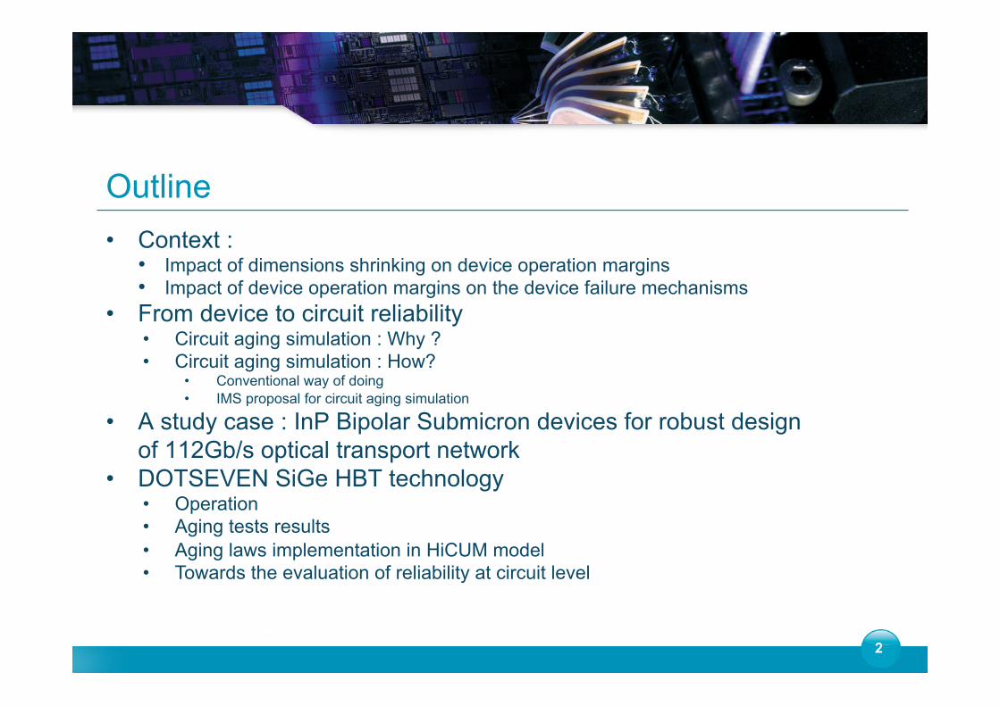
SiGe HBT basics : performances and scaling Ø Device performance is improved through reduction in transit time and
parasitic resistances and capacitances. Ø fT improvement is achieved through improvement in each of the delay
components, related to fT in the well-established approximation :
Ø fT is probably the most common figure of merit for an RF transistor. However, in many cases the fMAX figure of merit is more predictive for circuit performance.
5
SAT
CSCL
n
2B
CBECC
EBC
CSCLBCEECT 2
WDWCRR
qIkTC
qIkT
f21
υ+
γ+⎟⎟
⎠
⎞⎜⎜⎝
⎛+++≈τ+τ+τ+τ=τ=
π
CBB
TMAX CR8
fFπ
≈
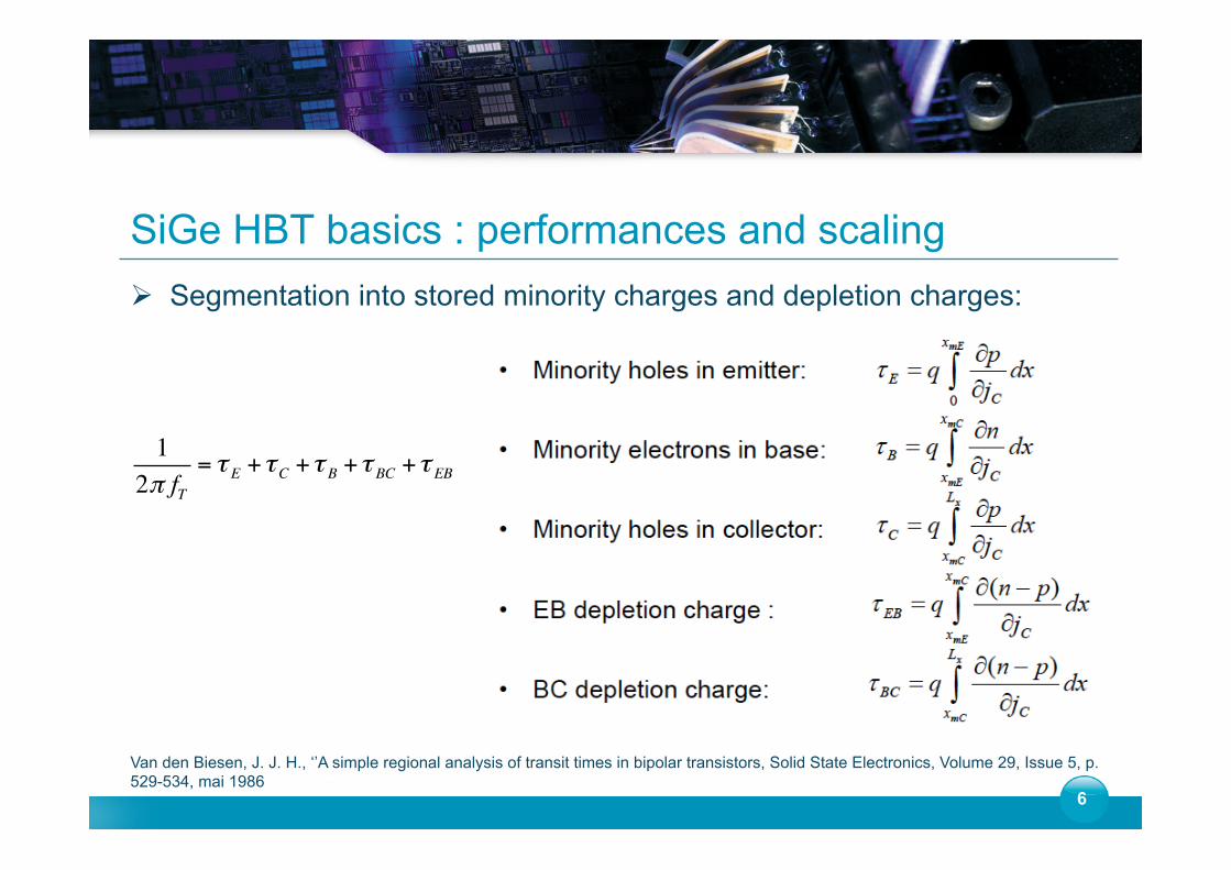
SiGe HBT basics : performances and scaling Ø Segmentation into stored minority charges and depletion charges:
6
12π fT
= τ E +τC +τ B +τ BC +τ EB
Van den Biesen, J. J. H., ‘’A simple regional analysis of transit times in bipolar transistors, Solid State Electronics, Volume 29, Issue 5, p. 529-534, mai 1986
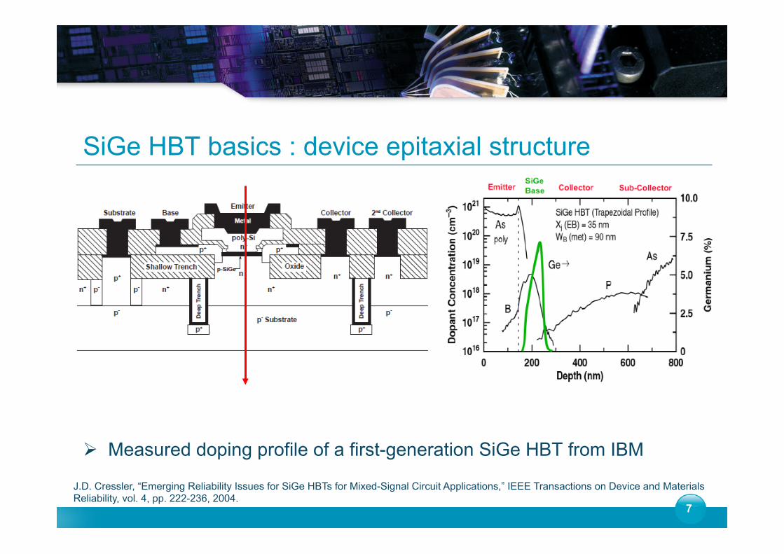
SiGe HBT basics : device epitaxial structure
Ø Measured doping profile of a first-generation SiGe HBT from IBM
7
J.D. Cressler, “Emerging Reliability Issues for SiGe HBTs for Mixed-Signal Circuit Applications,” IEEE Transactions on Device and Materials Reliability, vol. 4, pp. 222-236, 2004.
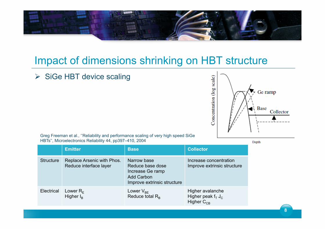
Impact of dimensions shrinking on HBT structure Ø SiGe HBT device scaling
8
Emitter Base Collector
Structure Replace Arsenic with Phos. Reduce interface layer
Narrow base Reduce base dose Increase Ge ramp Add Carbon Improve extrinsic structure
Increase concentration Improve extrinsic structure
Electrical Lower RE Higher IB
Lower VBE Reduce total RB
Higher avalanche Higher peak fT JC Higher CCB
Greg Freeman et al., ‘’Reliability and performance scaling of very high speed SiGe HBTs’’, Microelectronics Reliability 44, pp397–410, 2004

Effect of collector design
Ø (a) peak fT current density Ø (b) excess collector and base current from avalanche in the collector–
base space-charge region.
9
Greg Freeman et al., ‘’Reliability and performance scaling of very high speed SiGe HBTs’’, Microelectronics Reliability, 44, pp397–410, 2004

Bipolar reliability overview and performance trend related issues
10
Greg Freeman et al., ‘’Reliability and performance scaling of very high speed SiGe HBTs’’, Microelectronics Reliability, 44, pp397–410, 2004
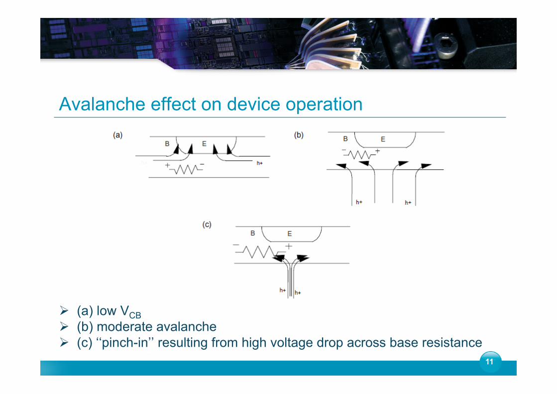
Avalanche effect on device operation
Ø (a) low VCB Ø (b) moderate avalanche Ø (c) ‘‘pinch-in’’ resulting from high voltage drop across base resistance
11

Hot carrier generation from avalanche and trapping in dielectric layers
Avalanche generated base current degradation for 200 GHz SiGe HBT Ø Emitter area: 0.12 x 2.0 µm2. Ø Stress conditions: VCB=2.5 V, IE=1.92 mA. Ø Before aging and after 8.3 h under the stress
12
IC
IB
After 8.3 h under stress Before aging
Greg Freeman et al., ‘’Reliability and performance scaling of very high speed SiGe HBTs’’, Microelectronics Reliability, 44, pp397–410, 2004

Safe Operating Area :SOA
13
• Safe Operating Area • High-performances HBT
fT/fMAX = 250/300 GHz • Common base configuration • Forced JE output characterictics • Breakdown voltages:
• BVCE0 = 1,7V • BVCB0 = 5,0V
G.G. Fischer , G. Sasso, “Ageing and thermal recovery of advanced SiGe heterojunction bipolar transistors under long-term mixed-mode and reverse stress conditions” Microelectronics Reliability 55, pp.498–507, 2015.
SOA HCI Ageing
Current Pinch-in
Electro-thermal Destruction
Outline • Context :
• Impact of dimensions shrinking on device operation margins • Impact of device operation margins on the device failure mechanisms
• From device to circuit reliability • Circuit aging simulation : Why ? • Circuit aging simulation : How?
• Conventional way of doing • IMS proposal for circuit aging simulation
• A study case : InP Bipolar Submicron devices for robust design of 112Gb/s optical transport network
• DOTSEVEN SiGe HBT technology • Operation • Aging tests results • Aging laws implementation in HiCUM model • Towards the evaluation of reliability at circuit level
14
15
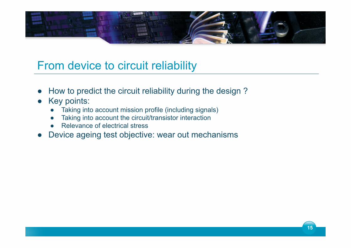
From device to circuit reliability
● How to predict the circuit reliability during the design ? ● Key points:
● Taking into account mission profile (including signals) ● Taking into account the circuit/transistor interaction ● Relevance of electrical stress
● Device ageing test objective: wear out mechanisms

Aging circuit simulation : why ?
16
Design Validation (simulation)
Reliability simulation
Correction loop
Prototype Electrical Tests
Reliability Tests Production
Design For Reliability : ü Predict during the design phase the effect of transistors and architecture
choices on the circuit reliability according to the application
Correction loop
Design time scale : weeks Prototype time scale : months
17
Vgs (V)
Vds (V) 0
1
2
3
4
5
6
7
0 1 2 3 4 5 6 7
VT
τ
Operationnal amplifier
VDD=5V
100 years 10 years
1 month
1 hour
1 year
1 day 6 hours
1 week
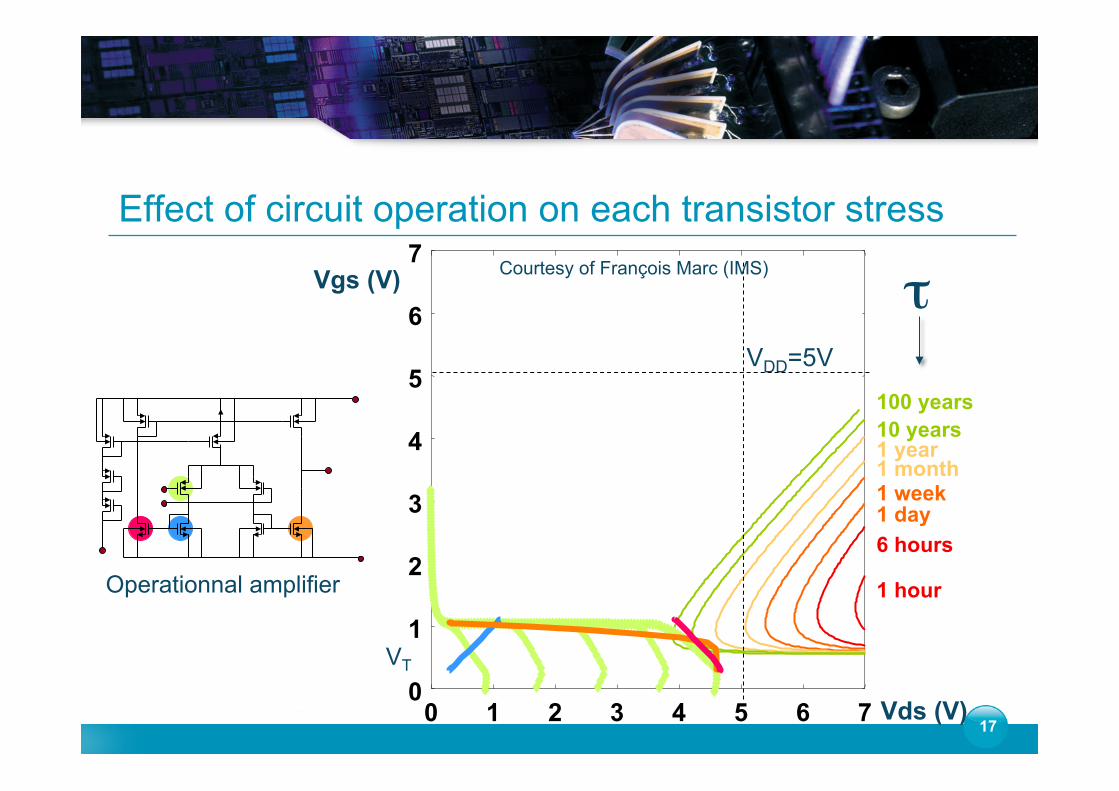
Effect of circuit operation on each transistor stress Courtesy of François Marc (IMS)
18
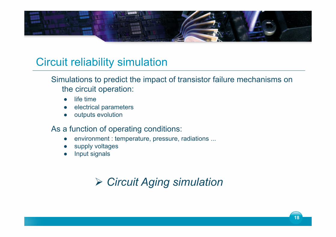
Circuit reliability simulation Simulations to predict the impact of transistor failure mechanisms on
the circuit operation: ● life time ● electrical parameters ● outputs evolution
As a function of operating conditions: ● environment : temperature, pressure, radiations ... ● supply voltages ● Input signals
Ø Circuit Aging simulation

19
Conventional approach : Design in Reliability (DiR)
Ø DiR model flow highlights interactions between simulator, stress computation program and model cards.
Model card Library
Conditions : Bias,
Temperature, Time, AC, DC, …
simulator
Stress computation Aged model card library
S.Ighilahriz et al., ’’Reliability study uner DC stress On mmW LNA, Mixer and VCO’’, IEEE International Reliability Physics Symposium (IRPS), 2012
20
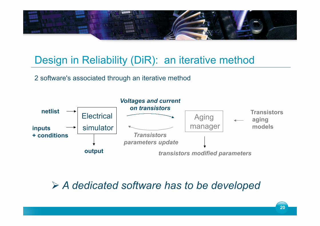
Design in Reliability (DiR): an iterative method 2 software's associated through an iterative method
Electrical simulator
Aging manager
Transistors parameters update
Voltages and current on transistors netlist Transistors
aging models inputs
+ conditions
output transistors modified parameters
Ø A dedicated software has to be developed

21
Circuit netlist Simulator
VHDL-AMS Ageing models
Transistor aging model • Based on the transistor compact model • Takes into account the aging models/laws/failure mechanisms (providing they are known) • Need to access to model code
inputs
outputs
Modified parameters of transistors
Circuit aging simulation : IMS approach A single simulator (with VHDL-AMS or Verilog-A)

22
Requirements for circuit aging simulation ● Use VHDL-AMS or Verilog-A to build compact models including aging
● Compact model code ● Add physical quantities in the compact model ● Implementation of the aging laws in the compact model
Ø Physics of failure Ø Ageing tests @ transistor level
● Change compact model parameters into (slowly) variable quantities Ø Parameters extraction of the failure laws
● Virtual acceleration of degradation mechanism to obtain electrical times (<1 second) and ageing time (> 1 week) in a same simulation
Ø Versatility and efficiency for ageing simulation
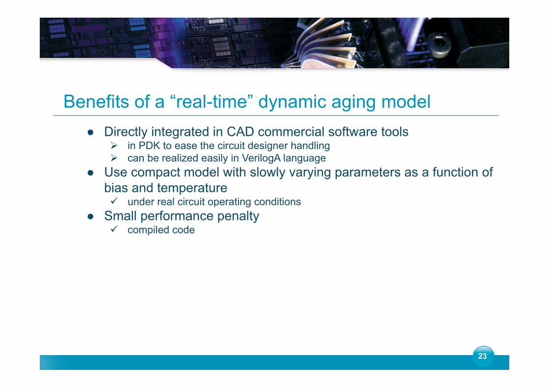
● Directly integrated in CAD commercial software tools Ø in PDK to ease the circuit designer handling Ø can be realized easily in VerilogA language
● Use compact model with slowly varying parameters as a function of bias and temperature ü under real circuit operating conditions
● Small performance penalty ü compiled code
23
Benefits of a “real-time” dynamic aging model

Outline • Context :
• Impact of dimensions shrinking on device operation margins • Impact of device operation margins on the device failure mechanisms
• From device to circuit reliability • Circuit aging simulation : Why ? • Circuit aging simulation : How?
• Conventional way of doing • IMS proposal for circuit aging simulation
• A study case : InP Bipolar Submicron devices for robust design of 112Gb/s optical transport network
• DOTSEVEN SiGe HBT technology • Operation • Aging tests results • Aging laws implementation in HiCUM model • Towards the evaluation of reliability at circuit level
24
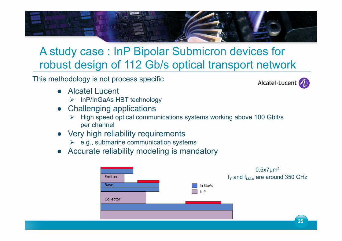
This methodology is not process specific
fT and fMAX are around 350 GHz 0.5x7µm2
25
● Alcatel Lucent Ø InP/InGaAs HBT technology
● Challenging applications Ø High speed optical communications systems working above 100 Gbit/s
per channel ● Very high reliability requirements
Ø e.g., submarine communication systems ● Accurate reliability modeling is mandatory
A study case : InP Bipolar Submicron devices for robust design of 112 Gb/s optical transport network

0.5x7µm2
26
InP HBT technologies • In general, less complicated implementation than Si
technologies Ø Two metal levels!Ø Triple mesa process technology!Ø Mesa isolation!
• Suffer from important self heating mechanism
Grandchamp et al., ‘’Trends in submicrometer InP-based HBT architecture targeting thermal management’’, IEEE Trans. On Electron Device, pp. 2566-2572 , Vol. 58, N°8, 2011.
Courtesy of Mohammed Zaknoune (IEMN)

Why choosing HiCuM L2 v2.30 compact model ?
• CMC labeled model (Available in most commercial simulators) • VerilogA code available • HiCuM accuracy + Specific improvements of version v2.30 • Modeling of advanced HBTs
Ø Parameter extraction for good initial model is already challenging
27
HiCuM compact model
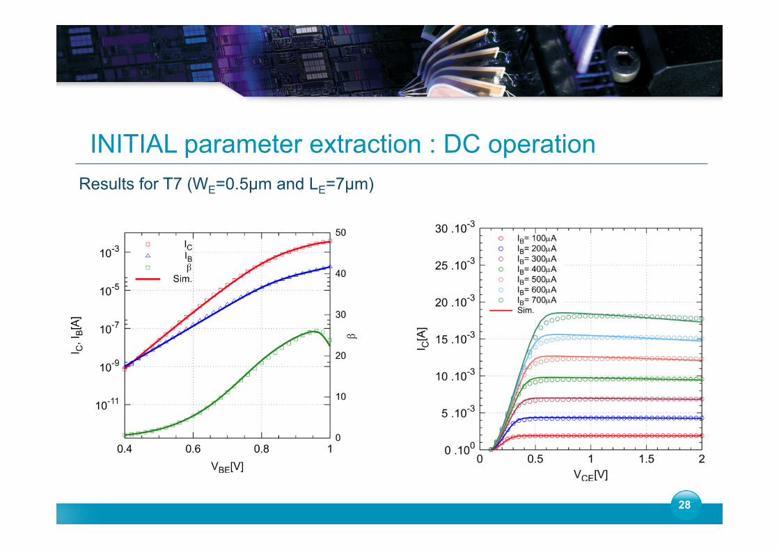
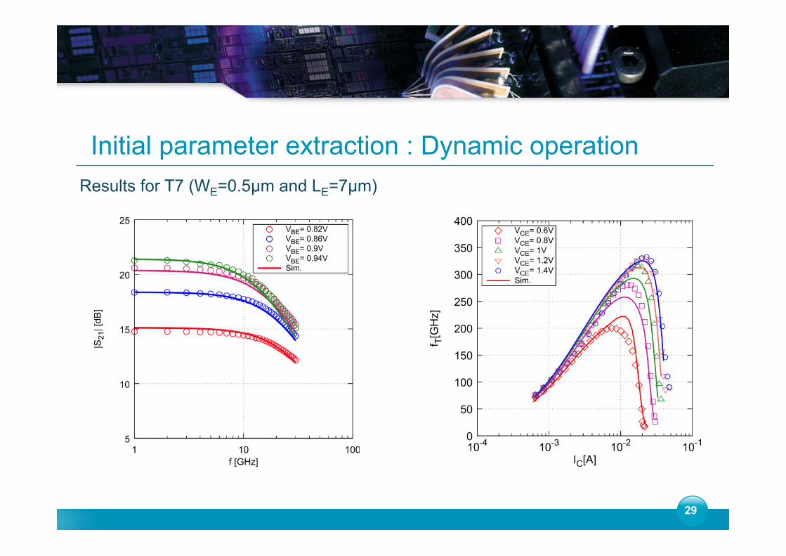
Results for T7 (WE=0.5µm and LE=7µm)
28
INITIAL parameter extraction : DC operation
29
Initial parameter extraction : Dynamic operation Results for T7 (WE=0.5µm and LE=7µm)
30
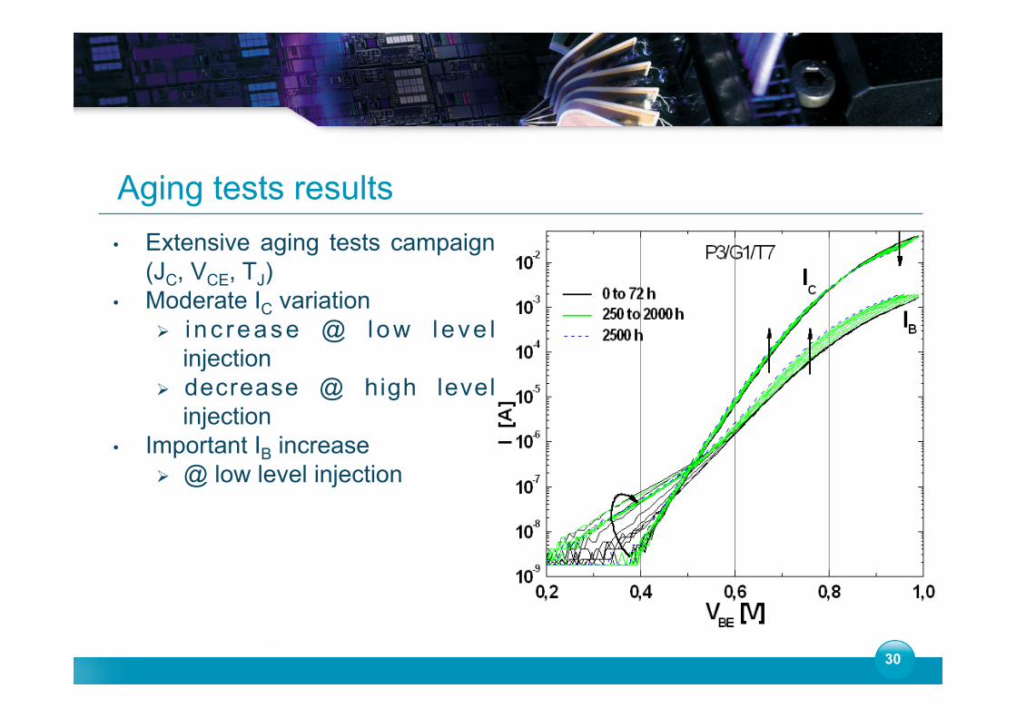
Aging tests results • Extensive aging tests campaign
(JC, VCE, TJ) • Moderate IC variation
Ø i n c rease @ low l eve l injection
Ø decrease @ high level injection
• Important IB increase Ø @ low level injection

ü Donor traps at E-B junction surroundings are responsible for the current variations
ü Trap concentration increase linearly with stress time
PassivationEmitter Contact
Base
Emitter
Collecteur
SubCollecteur
Emitter sidewall surface traps
Extrinsic base surface traps
Emitter-base interface traps
PassivationEmitter Contact
Base
Emitter
Collecteur
SubCollecteur
Emitter sidewall surface traps
Extrinsic base surface traps
Emitter-base interface traps
31
Extensive 2D/3D Calibrated TCAD Hydrodynamic simulations
Koné et al, ‘’Submicrometer InP/InGaAs DHBT Architecture Enhancements Targeting Reliability Improvements’’, IEEE Trans. On Electron Device, pp.1068-1074 , Vol. 60, N°3, 2013.
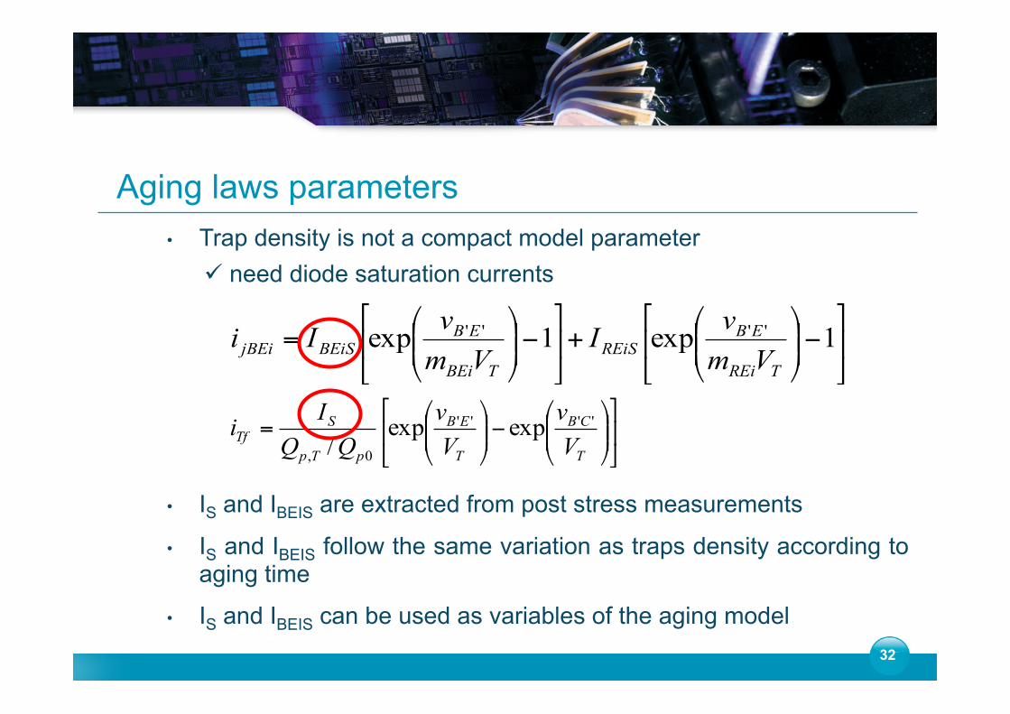
• Trap density is not a compact model parameter ü need diode saturation currents
• IS and IBEIS are extracted from post stress measurements
• IS and IBEIS follow the same variation as traps density according to aging time
• IS and IBEIS can be used as variables of the aging model
⎥⎦
⎤⎢⎣
⎡−⎟⎟⎠
⎞⎜⎜⎝
⎛+⎥⎦
⎤⎢⎣
⎡−⎟⎟⎠
⎞⎜⎜⎝
⎛= 1exp1exp ''''
TREi
EBREiS
TBEi
EBBEiSjBEi Vm
vIVm
vIi
⎥⎦
⎤⎢⎣
⎡⎟⎟⎠
⎞⎜⎜⎝
⎛−⎟⎟⎠
⎞⎜⎜⎝
⎛=
T
CB
T
EB
pTp
STf V
vVv
QQIi ''''
0,
expexp/
32
Aging laws parameters

• Donor trap density can be modeled as a generation mechanism ü Same holds for IBEis and IS
• Constant increasing rates follow an Arrhenius law
• BIBEIS , EIBEIS , BIS , EIS are new model parameters
),()(
Ctrap JTGdttdN=
),()(CIBEIS
BEiS JTAdttdI= ),()(
CISS JTAdttdI=
1exp),( αCJ
TkEBJTAB
IBEISIBEISCIBEIS ⎥
⎦
⎤⎢⎣
⎡⎟⎟⎠
⎞⎜⎜⎝
⎛−= 2exp),( α
CJ
TkEBJTAB
ISISCIS ⎥
⎦
⎤⎢⎣
⎡⎟⎟⎠
⎞⎜⎜⎝
⎛−=
33
Aging laws implementation
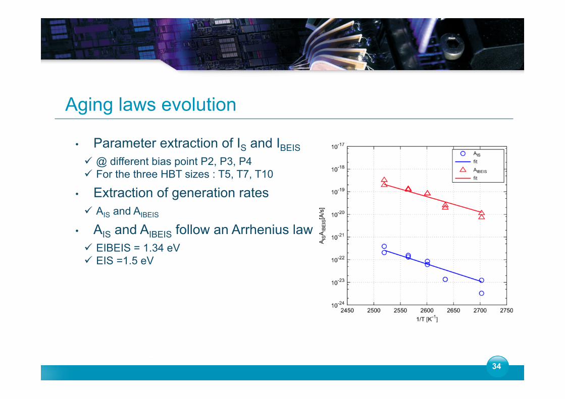
• Parameter extraction of IS and IBEIS ü @ different bias point P2, P3, P4 ü For the three HBT sizes : T5, T7, T10
• Extraction of generation rates ü AIS and AIBEIS
• AIS and AIBEIS follow an Arrhenius law ü EIBEIS = 1.34 eV ü EIS =1.5 eV
34
Aging laws evolution
Ibeis_out
Is_out
AIBEIS
AIS
C=1
C=1
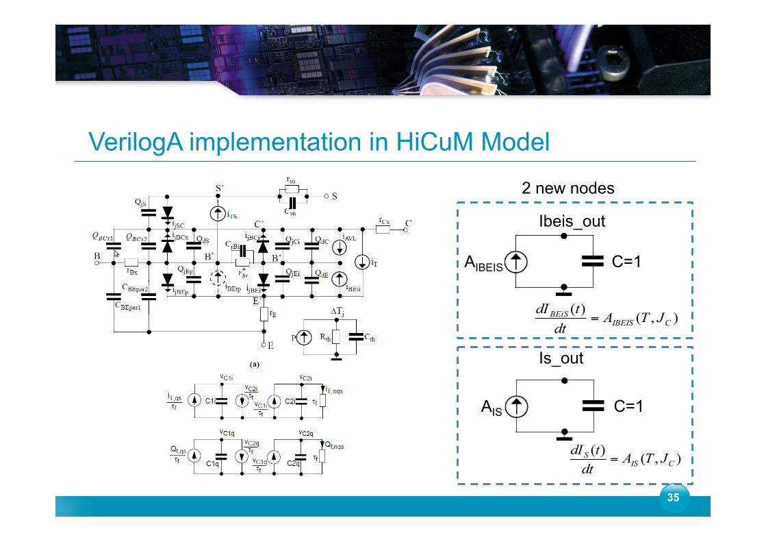
2 new nodes
),()(CIBEIS
BEiS JTAdttdI=
),()(CIS
S JTAdttdI=
35
VerilogA implementation in HiCuM Model
I(br_ibeisout) <+ -aibeis; I(br_ibeisout) <+ ddt(V(br_ibeisout));
I(br_isout) <+ -ais; I(br_isout) <+ ddt(V(br_isout));
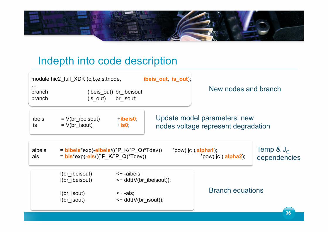
module hic2_full_XDK (c,b,e,s,tnode, ibeis_out, is_out); … branch (ibeis_out) br_ibeisout branch (is_out) br_isout;
aibeis = bibeis*exp(-eibeis/((`P_K/`P_Q)*Tdev)) *pow( jc ),alpha1); ais = bis*exp(-eis/((`P_K/`P_Q)*Tdev)) *pow( jc ),alpha2);
ibeis = V(br_ibeisout) +ibeis0; is = V(br_isout) +is0;
New nodes and branch
Update model parameters: new nodes voltage represent degradation
Temp & JC dependencies
Branch equations
36
Indepth into code description

I(br_ibeisout) <+ -atsf * aibeis; I(br_ibeisout) <+ ddt(V(br_ibeisout));
I(br_isout) <+ -atsf * ais; I(br_isout) <+ ddt(V(br_isout));
module hic2_full_XDK (c,b,e,s,tnode, ibeis_out, is_out); … branch (ibeis_out) br_ibeisout branch (is_out) br_isout;
aibeis = bibeis*exp(-eibeis/((`P_K/`P_Q)*Tdev)) *pow( jc ),alpha1); ais = bis*exp(-eis/((`P_K/`P_Q)*Tdev)) *pow( jc ),alpha2);
ibeis = V(br_ibeisout) +ibeis0; is = V(br_isout) +is0;
ATSF : Accelerating Time Scale Factor new parameter ATSF=3.6E13 100ns è1000 h ATSF=3.15E15 100ns è10 years
Simulation of degradations is too slow: 10000 years of CPU time !!!
37
Indepth into Code description cont’
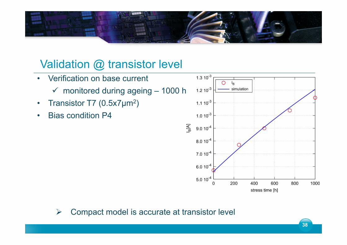
• Verification on base current ü monitored during ageing – 1000 h
• Transistor T7 (0.5x7µm2) • Bias condition P4
38
Validation @ transistor level
Ø Compact model is accurate at transistor level

Transimpedance input stage
Cherry-Hooper amplifier
50-Ω output bufferDifferential amplifier
Low frequency (~DC)offset compensation amplifier
Low pass filter
INPUT
Differential OUTPUT
VCC
External capacitor
Referencevoltage
RFB
RCLPeaking
VTIA
VREF
39
@ Circuit level : Transimpedance Amplifier (TIA) Ø Featuring complex offest compensation loop

• 2 versions of the TIA available for aging tests ü TLIA (high DC gain – low cutoff frequency) ü TIA-HF (lower DC gain – Higher bandwidth) ü 22 circuits samples submitted to accelerated aging test for 1008 hours ü Chuck temperature = 70°C ü Tj up 125°C
40
TIA description

• Measurements versus simulations
• Perl scripting is used to automate ’’aged’’ circuit simulation
• Software : Agilent ADS
ü Excellent initial model ü Slightly pessimistic aging ü But fairly accurate
predictions
41
TLIA S parameters measured up to 65GHz
Ardouin et al., ‘’ Advancements on reliability-aware analog circuit design’’, Invited paper, Solid-State Device Research Conference (ESSDERC), 2012 Proceedings of the European, pp.62-68, 17-21 Sept 2012,

• ATSF=36x1012 (100ns=10years) • Temperature=100°C • Dynamic observation of all circuit nodes
ü Differential output voltage (S-Sb) • Circuit instances can be extracted at any
time step
42
@ Circuit level : TLIA Transient simulation
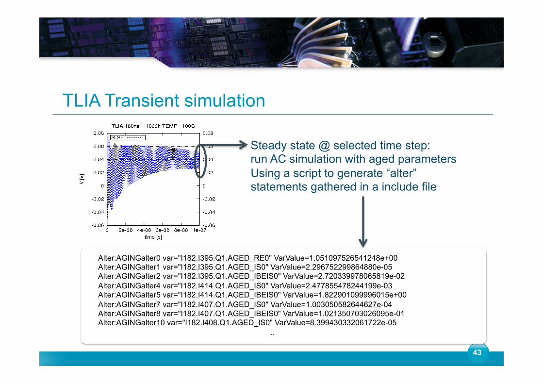
Steady state @ selected time step: run AC simulation with aged parameters Using a script to generate “alter” statements gathered in a include file
Alter:AGINGalter0 var="I182.I395.Q1.AGED_RE0" VarValue=1.051097526541248e+00 Alter:AGINGalter1 var="I182.I395.Q1.AGED_IS0" VarValue=2.296752299864880e-05 Alter:AGINGalter2 var="I182.I395.Q1.AGED_IBEIS0" VarValue=2.720339978065819e-02 Alter:AGINGalter4 var="I182.I414.Q1.AGED_IS0" VarValue=2.477855478244199e-03 Alter:AGINGalter5 var="I182.I414.Q1.AGED_IBEIS0" VarValue=1.822901099996015e+00 Alter:AGINGalter7 var="I182.I407.Q1.AGED_IS0" VarValue=1.003050582644627e-04 Alter:AGINGalter8 var="I182.I407.Q1.AGED_IBEIS0" VarValue=1.021350703026095e-01 Alter:AGINGalter10 var="I182.I408.Q1.AGED_IS0" VarValue=8.399430332061722e-05
..
43
TLIA Transient simulation
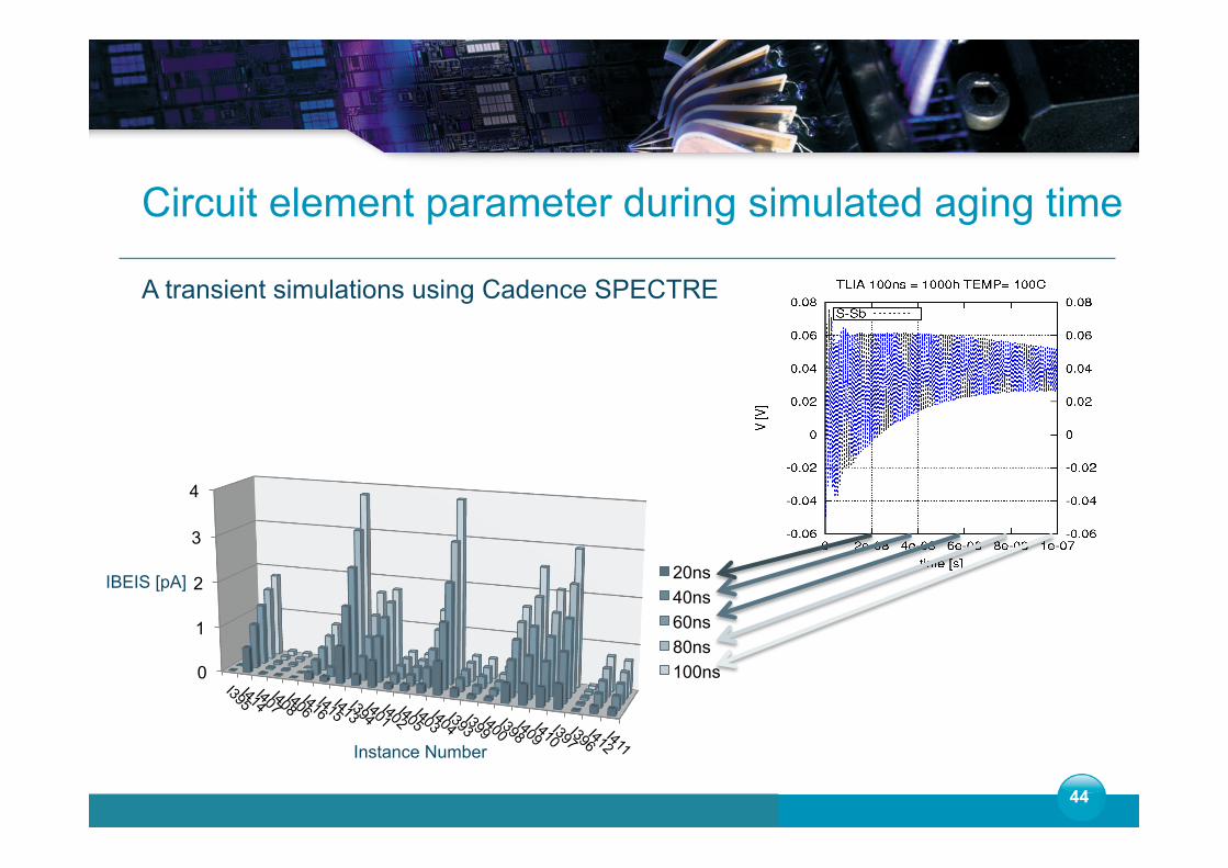
0
1
2
3
4
IBEIS [pA]
Instance Number
20ns 40ns 60ns 80ns 100ns
44
Circuit element parameter during simulated aging time A transient simulations using Cadence SPECTRE

0
1
2
3
4
IBEIS [pA]
Instance Number
Transimpedance input stage
Cherry-Hooper amplifier
50-Ω output bufferDifferential amplifier
Low frequency (~DC)offset compensation amplifier
Low pass filter
INPUT
Differential OUTPUT
VCC
External capacitor
Referencevoltage
RFB
RCLPeaking
45
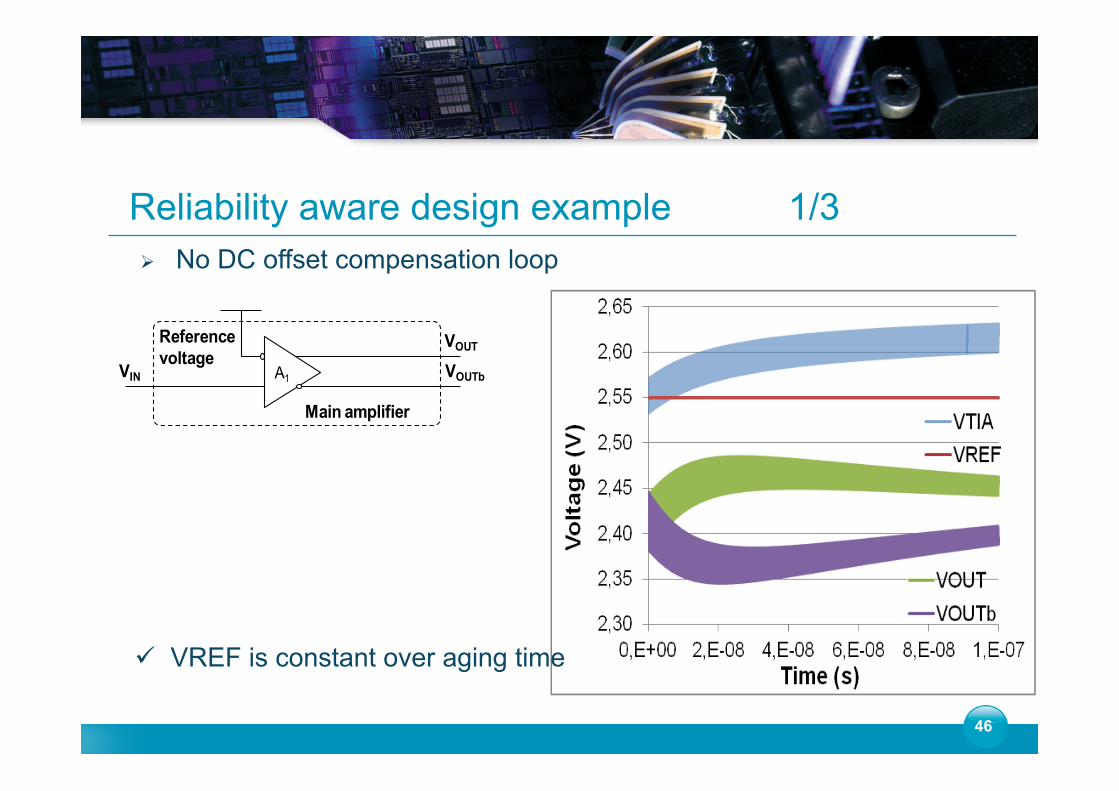
Ø No DC offset compensation loop
VIN
Main amplifier
Referencevoltage
VOUT
VOUTbA1
ü VREF is constant over aging time
46
Reliability aware design example 1/3
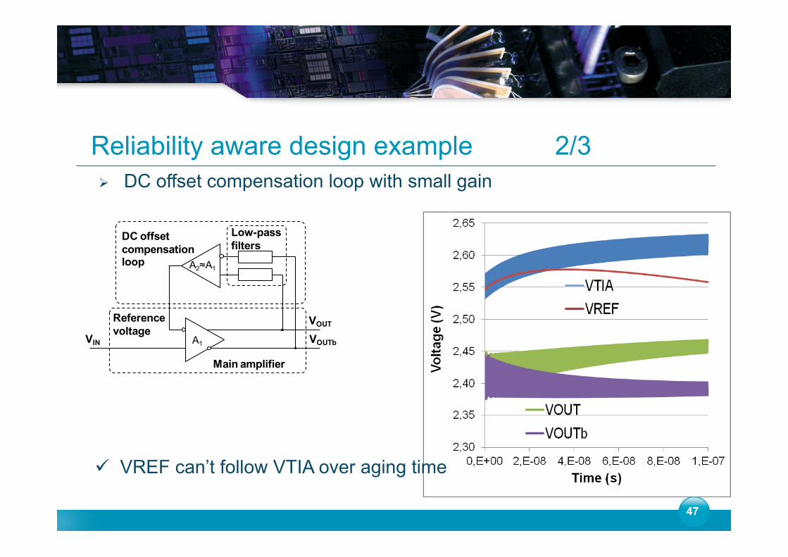
Ø DC offset compensation loop with small gain
DC offset compensation loop
Low-passfilters
Main amplifier
A2≈A1
VIN
Referencevoltage
A1
VOUT
VOUTb
ü VREF can’t follow VTIA over aging time
47
Reliability aware design example 2/3
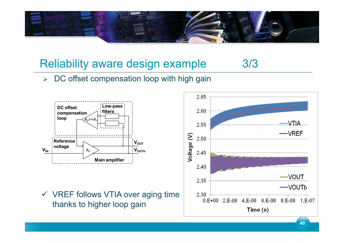
Ø DC offset compensation loop with high gain
DC offset compensation loop
Low-passfilters
Main amplifier
A1
A2>>A1
VIN
Referencevoltage
VOUT
VOUTb
ü VREF follows VTIA over aging time thanks to higher loop gain
48
Reliability aware design example 3/3
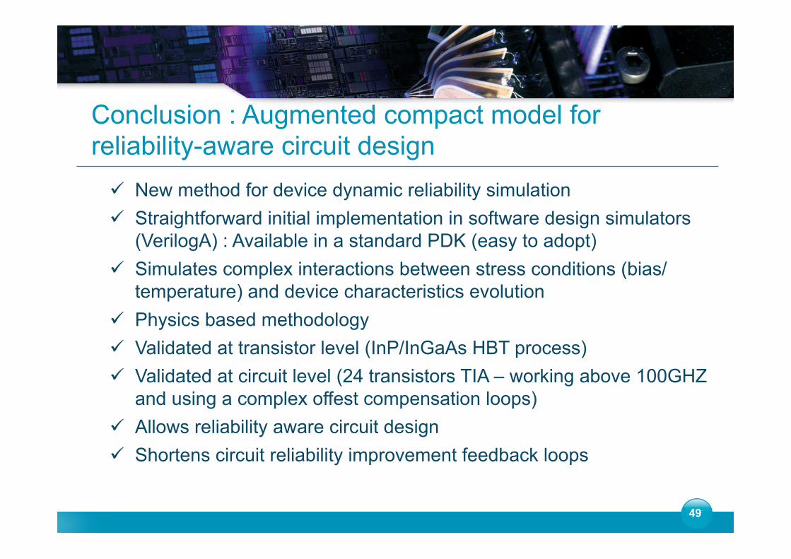
ü New method for device dynamic reliability simulation ü Straightforward initial implementation in software design simulators
(VerilogA) : Available in a standard PDK (easy to adopt) ü Simulates complex interactions between stress conditions (bias/
temperature) and device characteristics evolution ü Physics based methodology ü Validated at transistor level (InP/InGaAs HBT process) ü Validated at circuit level (24 transistors TIA – working above 100GHZ
and using a complex offest compensation loops) ü Allows reliability aware circuit design ü Shortens circuit reliability improvement feedback loops
49
Conclusion : Augmented compact model for reliability-aware circuit design

Outline • Context :
• Impact of dimensions shrinking on device operation margins • Impact of device operation margins on the device failure mechanisms
• From device to circuit reliability • Circuit aging simulation : Why ? • Circuit aging simulation : How?
• Conventional way of doing • IMS proposal for circuit aging simulation
• A study case : InP Bipolar Submicron devices for robust design of 112Gb/s optical transport network
• DOTSEVEN SiGe HBT technology • Operation • Aging tests results • Aging laws implementation in HiCUM model • Towards the evaluation of reliability at circuit level
50
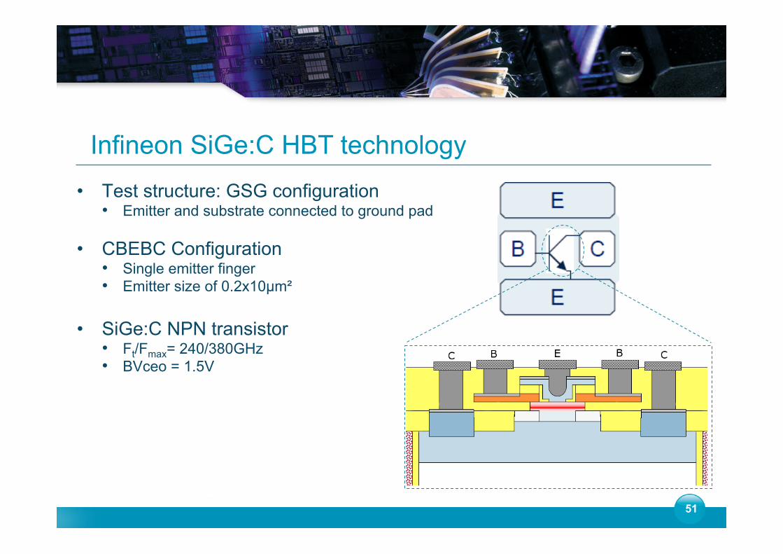
• Test structure: GSG configuration • Emitter and substrate connected to ground pad
• CBEBC Configuration • Single emitter finger • Emitter size of 0.2x10µm²
• SiGe:C NPN transistor • Ft/Fmax= 240/380GHz • BVceo = 1.5V
51
Infineon SiGe:C HBT technology

Device under test: DC characterization
52
0.4 0.5 0.6 0.7 0.8 0.9 1.010-‐12
10 -‐11
10 -‐10
10 -‐9
10 -‐8
10 -‐7
10 -‐6
10 -‐5
10 -‐4
10 -‐3
10 -‐2
10 -‐1
200
400
600
800
1000
1200
AE ,eff
= 1x0.11x9.93 µm²
I C, I
B [A]
VB E [V ]
Meas urement H IC UM
Curren
t Gain (β)
0.3 0.4 0.5 0.6 0.7 0.8 0.9 1.010-12
10-10
10-8
10-6
10-4
10-2
10010-1210-1110-1010-9 10-8 10-7 10-6 10-5 10-4 10-3 10-2 10-1 100
10
100
1000
Cur
rent
(A)
VBE (V)
0 .11x9.93µm² 0 .13x9.93µm²IB
IC (A)
βIC
0.0 0.2 0.4 0.6 0.8 1.0 1.2 1.40
1
2
3
4
Meas urement H IC UM
I C [mA]
VC E [V ]
IB=0.5 to 10µA
(in s tep of 0.95µA)
0.0 0.2 0.4 0.6 0.8 1.0 1.2 1.40
2
4
6
8
10
12
14
Meas urement H IC UM
I C [mA]
VC E [V ]
VB E=0.6 to0.9V
(in s tep of 0.05V)

Aging test campaigns
53
• Requirements : to identify wear out mechanisms • Slowly evolving with time • At the edge of the Safe Operating Area
• Long-time stress tests (i.e. 1000 h) • Stress tests and measurements realized using encapsulated devices • Samples biased in a common-emitter configuration at constant and controlled ambient
temperature of 300K.
• Evolution characterization • DC characterization is performed at fixed time of 1h, 3h, 7h, 24h, 36h, 48h, 72h, 120h,
250h, 500h, 750h and 1000h. • At 300h, an additional point is added with 24h between the end of the stress test and
the measurement èEvaluation of recovery mechanism • Base-emitter junction characterization : forward Gummel plot at Vbc=0V • Base-collector junction characterization : Reverse Gummel plot at Vbe=0V
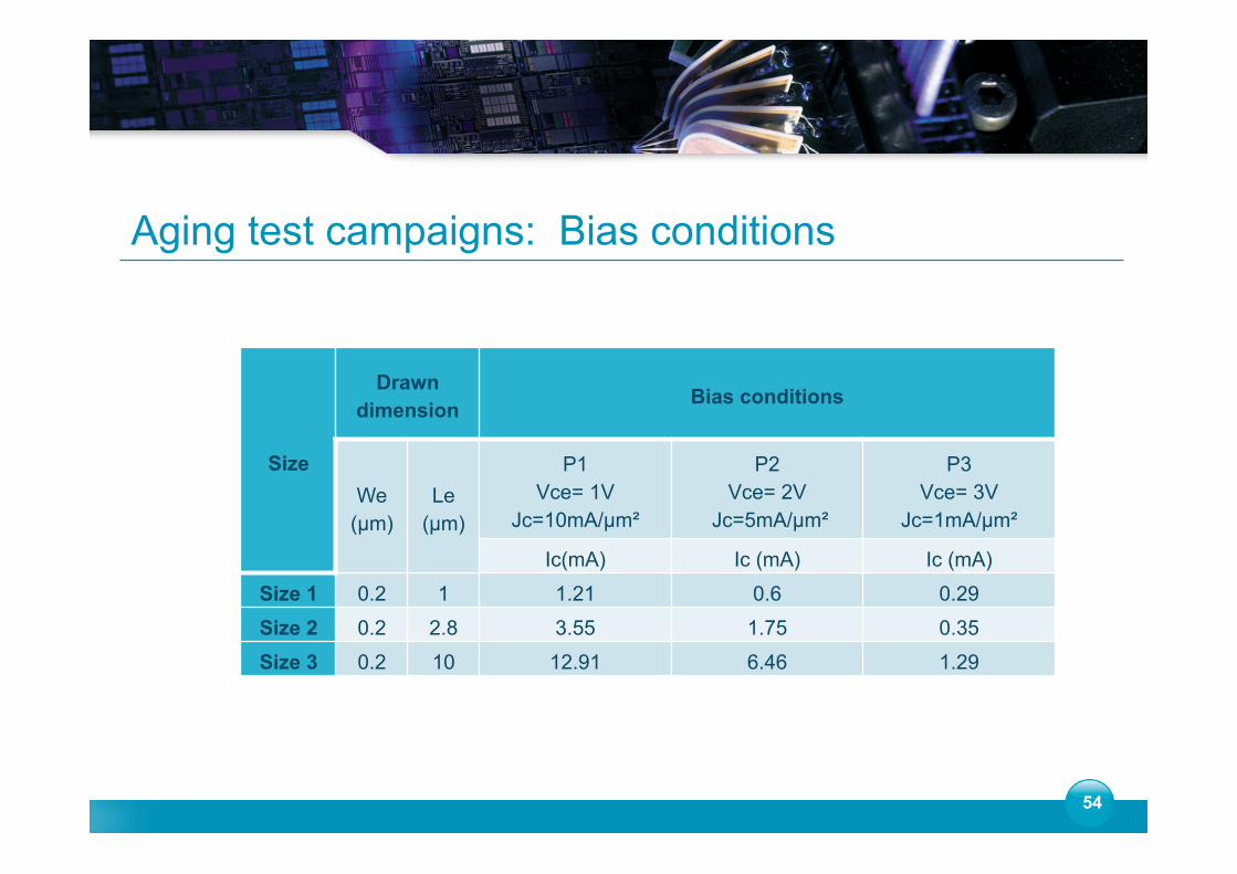
Aging test campaigns: Bias conditions
54
Size
Drawn dimension Bias conditions
We (µm)
Le (µm)
P1 Vce= 1V
Jc=10mA/µm²
P2 Vce= 2V
Jc=5mA/µm²
P3 Vce= 3V
Jc=1mA/µm²
Ic(mA) Ic (mA) Ic (mA)
Size 1 0.2 1 1.21 0.6 0.29
Size 2 0.2 2.8 3.55 1.75 0.35
Size 3 0.2 10 12.91 6.46 1.29
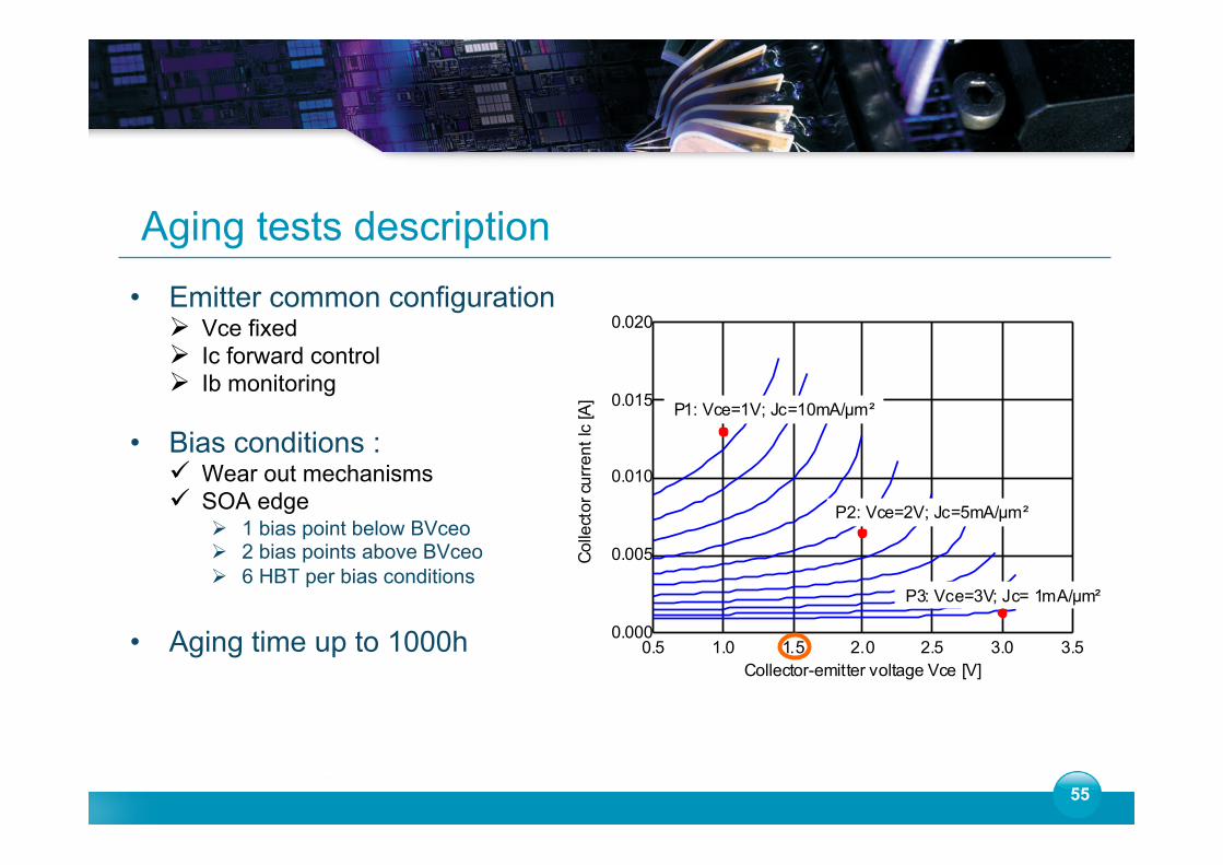
• Emitter common configuration Ø Vce fixed Ø Ic forward control Ø Ib monitoring
• Bias conditions : ü Wear out mechanisms ü SOA edge
Ø 1 bias point below BVceo Ø 2 bias points above BVceo Ø 6 HBT per bias conditions
• Aging time up to 1000h
55
Aging tests description
0.5 1.0 1.5 2.0 2.5 3.0 3.50.000
0.005
0.010
0.015
0.020
Col
lect
or cu
rrent
Ic [A
]
Collector-emitter voltage Vce [V]
P1: Vce=1V; Jc=10mA/µm²
P2: Vce=2V; Jc=5mA/µm²
P3: Vce=3V; Jc= 1mA/µm²
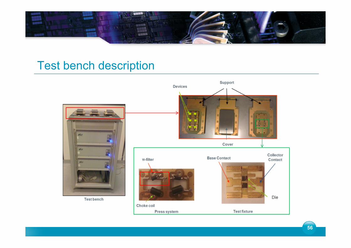
Test bench description
56

0.4 0.5 0.6 0.7 0.8 0.9 1.010-9
10-8
10-7
10-6
10-5
10-4
10-3
10-2
10-1
10-9
10-8
10-7
10-6
10-5
10-4
10-3
10-2
10-1
0h 1h 3h 7h 17h 24h 36h 48h 72h 120h 250h 300h 500h 750h 1000h
Base
and
coll
ecto
r cur
rent
[A]
Base-emitter voltage Vbe [V]
1000h
0h
Ic
Ib
Vbc=0V
Vbe
=0.6
5V
57
Aging tests results
1 10 100 1000-2.0x10⁻⁸
0.0
2.0x10⁻⁸
4.0x10⁻⁸
6.0x10⁻⁸
8.0x10⁻⁸
1.0x10⁻⁷
1.2x10⁻⁷
1.4x10⁻⁷
ΔIb
(t) =
Ib(t)
- Ib
(0)
Aging time [h]
ΔIb(t) @ Vbe=0.65V
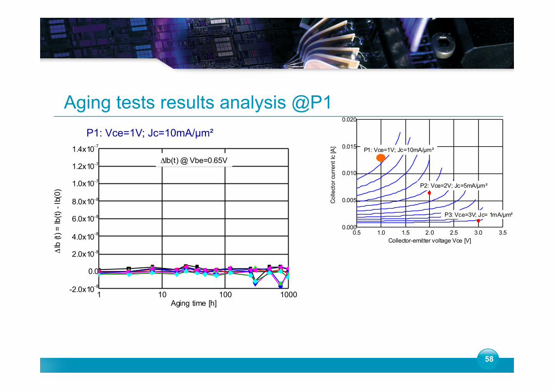
P1: Vce=1V; Jc=10mA/µm²
58
Aging tests results analysis @P1
0.5 1.0 1.5 2.0 2.5 3.0 3.50.000
0.005
0.010
0.015
0.020
Col
lect
or cu
rrent
Ic [A
]
Collector-emitter voltage Vce [V]
P1: Vce=1V; Jc=10mA/µm²
P2: Vce=2V; Jc=5mA/µm²
P3: Vce=3V; Jc= 1mA/µm²
59
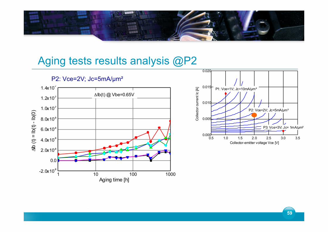
Aging tests results analysis @P2
0.5 1.0 1.5 2.0 2.5 3.0 3.50.000
0.005
0.010
0.015
0.020
Col
lect
or cu
rrent
Ic [A
]
Collector-emitter voltage Vce [V]
P1: Vce=1V; Jc=10mA/µm²
P2: Vce=2V; Jc=5mA/µm²
P3: Vce=3V; Jc= 1mA/µm²
1 10 100 1000-2.0x10⁻⁸
0.0
2.0x10⁻⁸
4.0x10⁻⁸
6.0x10⁻⁸
8.0x10⁻⁸
1.0x10⁻⁷
1.2x10⁻⁷
1.4x10⁻⁷
ΔIb(t) @ Vbe=0.65V
ΔIb
(t) =
Ib(t)
- Ib
(0)
Aging time [h]
P2: Vce=2V; Jc=5mA/µm²

60
Aging tests results analysis @P3
0.5 1.0 1.5 2.0 2.5 3.0 3.50.000
0.005
0.010
0.015
0.020
Col
lect
or cu
rrent
Ic [A
]
Collector-emitter voltage Vce [V]
P1: Vce=1V; Jc=10mA/µm²
P2: Vce=2V; Jc=5mA/µm²
P3: Vce=3V; Jc= 1mA/µm²
1 10 100 1000-2.0x10⁻⁸
0.0
2.0x10⁻⁸
4.0x10⁻⁸
6.0x10⁻⁸
8.0x10⁻⁸
1.0x10⁻⁷
1.2x10⁻⁷
1.4x10⁻⁷
ΔIb(t) @ Vbe=0.65V
ΔIb
(t) =
Ib(t)
- Ib
(0)
Aging time [h]
P3: Vce=3V; Jc=1mA/µm²

High Vce (>BVceo)
Electrons accelerate in BC
space region
Creation of electron-hole pairs (Impact ionization)
Hot carriers injected in E-B
spacer
Carriers break dangling bond *
Increase of trap density
-
-
+
61
• Z. Chendong et al., Damage mechanisms in impact-ionization-induced mixed-mode reliability degradation of SiGe HBTs’’, IEEE Transaction on Device and Materials Reliability, vol. 5, n. 1, March 2005, pp 142-149.
Aging mechanism analysis

• Uniform acceptor type trap density Ø Trap energy level: ET-EV=0.6 eV
Trap density location
62
Trap density simulation
Schroder et al., ‘’Negative bias temperature instability: Road to cross in deep submicron silicon semiconductor manufacturing’’, J. Appl. Phys. 94(1), 2003

• At each stress time, extraction of trap density • Evolution of trap density
0 100 200 300 400 500 600 700 800 900 10005.0x1011
1.0x10¹²
1.5x10¹²
2.0x10¹²
2.5x10¹²
NT [
cm-2]
Aging Time [h]
Trap density @ P2 Trap density @ P3 Exponential fitting
63
Trap density evolution

• HiCuM compact model L2 Ø Version 2.33
• E-B junction periphery Ø Trap location
• IREpS parameter converted as a new variable in HiCuM
exp 1 exp 1BE BEjBEp BEpS REpS
BEp T REp T
v vi I Im V m V
⎡ ⎤ ⎡ ⎤⎛ ⎞ ⎛ ⎞= − + −⎢ ⎥ ⎢ ⎥⎜ ⎟ ⎜ ⎟⎜ ⎟ ⎜ ⎟⎢ ⎥ ⎢ ⎥⎝ ⎠ ⎝ ⎠⎣ ⎦ ⎣ ⎦
, , ,( ) exp( )REpS REpS final REpS initial REpS finaltI I I Iτ
= + − −
64
Compact modeling
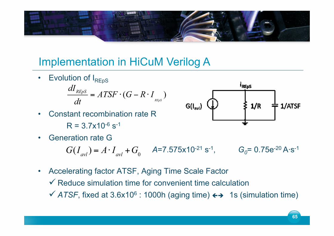
• Evolution of IREpS
• Constant recombination rate R R = 3.7x10⁻⁶ s-1
• Generation rate G A=7.575x10⁻²¹ s-1, G0= 0.75e-20 A·s-1
• Accelerating factor ATSF, Aging Time Scale Factor ü Reduce simulation time for convenient time calculation ü ATSF, fixed at 3.6x10⁶ : 1000h (aging time) çè 1s (simulation time)
65
Implementation in HiCuM Verilog A
dIREpSdt
= ATSF ⋅ (G − R ⋅ IREpS)
G(Iavl ) = A ⋅ Iavl +G0

0 200 400 600 800 10000.0
4.0x10⁻¹⁵
8.0x10⁻¹⁵
1.2x10⁻¹⁴
1.6x10⁻¹⁴
2.0x10⁻¹⁴
I REp
S
Aging time (tsim x ATSF) [h]
IREpS P3
Simulation results • Same conditions as P3 bias point
66
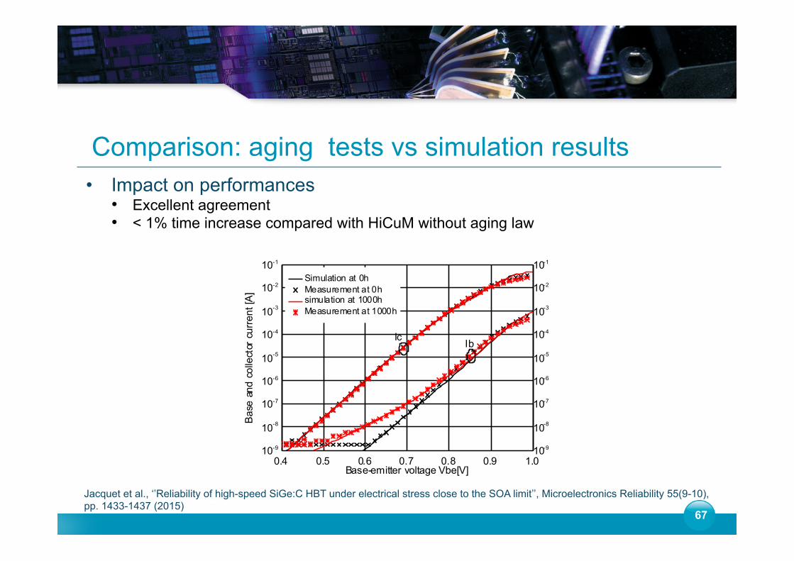
Comparison: aging tests vs simulation results
67
• Impact on performances • Excellent agreement • < 1% time increase compared with HiCuM without aging law
0.4 0.5 0.6 0.7 0.8 0.9 1.010-9
10-8
10-7
10-6
10-5
10-4
10-3
10-2
10-1
10-9
10-8
10-7
10-6
10-5
10-4
10-3
10-2
10-1
Simulation at 0h Measurement at 0h simulation at 1000h Measurement at 1000h
Bas
e an
d co
llect
or c
urre
nt [A
]
Base-emitter voltage Vbe[V]
IcIb
Jacquet et al., ‘’Reliability of high-speed SiGe:C HBT under electrical stress close to the SOA limit’’, Microelectronics Reliability 55(9-10), pp. 1433-1437 (2015)
Reliability study at circuit level
• Validation of SiGe:C HBT compact model for reliability study at circuit level ü Aging tests performed on single finger HBT ü Analysis using 2D TCAD simulation (collaboration with UN) ü Implantation of HBT failure laws into the compact model (HiCUM)
• Further investigations on HBT failure mechanisms Ø Self heating impact
• Targeted SiGe:C HBT Circuits • Power Amplifier (PA) • Low-Noise Amplifier (LNA) • Voltage Controlled Oscillator (VCO)
68
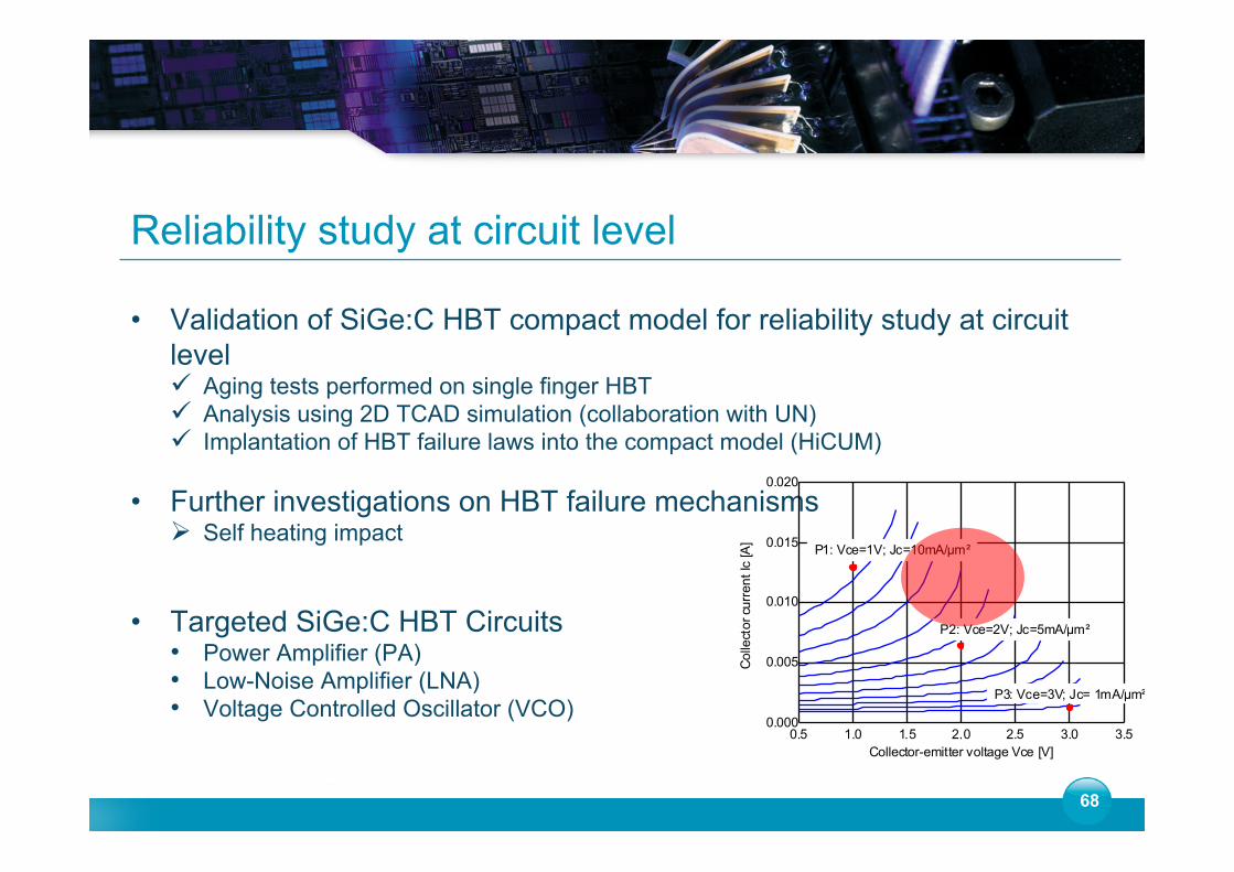
0.5 1.0 1.5 2.0 2.5 3.0 3.50.000
0.005
0.010
0.015
0.020
Col
lect
or cu
rrent
Ic [A
]Collector-emitter voltage Vce [V]
P1: Vce=1V; Jc=10mA/µm²
P2: Vce=2V; Jc=5mA/µm²
P3: Vce=3V; Jc= 1mA/µm²

Acknowledgement ● This project has received funding from the European Union's Seventh
Programme for research, technological development and demonstration under grant agreement No 316755.
69
Related Documents