FN6548 Rev 6.00 Page 1 of 26 November 22, 2013 FN6548 Rev 6.00 November 22, 2013 ISL28006 Micropower, Rail to Rail Input Current Sense Amplifier with Voltage Output DATASHEET The ISL28006 is a micropower, uni-directional high-side and low-side current sense amplifier featuring a proprietary rail-to-rail input current sensing amplifier. The ISL28006 is ideal for high-side current sense applications where the sense voltage is usually much higher than the amplifier supply voltage. The device can be used to sense voltages as high as 28V when operating from a supply voltage as low as 2.7V. The micropower ISL28006 consumes only 50μA of supply current when operating from a 2.7V to 28V supply. The ISL28006 features a common-mode input voltage range from 0V to 28V. The proprietary architecture extends the input voltage sensing range down to 0V, making it an excellent choice for low-side ground sensing applications. The benefit of this architecture is that a high degree of total output accuracy is maintained over the entire 0V to 28V common mode input voltage range. The ISL28006 is available in fixed (100V/V, 50V/V, 20V/V and Adjustable) gains in the space saving 5 Ld SOT-23 package and the 6 Ld SOT-23 package for the adjustable gain part. The parts operate over the extended temperature range from -40°C to +125°C. Features • Low Power Consumption. . . . . . . . . . . . . . . . . . . . . . 50μA, Typ • Supply Range . . . . . . . . . . . . . . . . . . . . . . . . . . . . . . 2.7V to 28V • Wide Common Mode Input . . . . . . . . . . . . . . . . . . . . 0V to 28V • Gain Versions - ISL28006-100 . . . . . . . . . . . . . . . . . . . . . . . . . . . . . . 100V/V - ISL28006-50 . . . . . . . . . . . . . . . . . . . . . . . . . . . . . . . . 50V/V - ISL28006-20 . . . . . . . . . . . . . . . . . . . . . . . . . . . . . . . . 20V/V - ISL28006-ADJ . . . . . . . . . . . . . . . . ADJ (Min Gain = 20V/V) • Operating Temperature Range . . . . . . . . . . . . -40°C to +125°C • Packages. . . . . . . . . . . . . . . . . . . . . . 5 Ld SOT-23, 6 Ld SOT-23 Applications • Power Management/Monitors • Power Distribution and Safety • DC/DC, AC/DC Converters • Battery Management/Charging • Automotive Power Distribution Related Literature • See AN1532 for “ISL28006 Evaluation Board User’s Guide” FIGURE 1. TYPICAL APPLICATION FIGURE 2. GAIN ACCURACY vs V RS+ = 0V TO 28V ISL28006 GND ISL28006 ISL28006 +5VDC +12VDC + - +1.0VDC +1.0VDC SENSE SENSE SENSE OUTPUT +5VDC OUTPUT +12VDC OUTPUT MULTIPLE OUTPUT POWER SUPPLY I SENSE +12VDC I SENSE +5VDC I SENSE +1.0VDC + - + - R SENSE +5VDC +5VDC +5VDC R SENSE R SENSE 0 2 4 6 8 10 12 14 16 18 20 22 24 26 28 ACCURACY (%) -1.4 -1.2 -1 -0.8 -0.6 -0.4 -0.2 0 0.2 0.4 0.6 V RS+ (V) +100°C +25°C -40°C +125°C GAIN 100

Welcome message from author
This document is posted to help you gain knowledge. Please leave a comment to let me know what you think about it! Share it to your friends and learn new things together.
Transcript

FN6548Rev 6.00
November 22, 2013
ISL28006Micropower, Rail to Rail Input Current Sense Amplifier with Voltage Output
DATASHEET
The ISL28006 is a micropower, uni-directional high-side and low-side current sense amplifier featuring a proprietary rail-to-rail input current sensing amplifier. The ISL28006 is ideal for high-side current sense applications where the sense voltage is usually much higher than the amplifier supply voltage. The device can be used to sense voltages as high as 28V when operating from a supply voltage as low as 2.7V. The micropower ISL28006 consumes only 50µA of supply current when operating from a 2.7V to 28V supply.
The ISL28006 features a common-mode input voltage range from 0V to 28V. The proprietary architecture extends the input voltage sensing range down to 0V, making it an excellent choice for low-side ground sensing applications. The benefit of this architecture is that a high degree of total output accuracy is maintained over the entire 0V to 28V common mode input voltage range.
The ISL28006 is available in fixed (100V/V, 50V/V, 20V/V and Adjustable) gains in the space saving 5 Ld SOT-23 package and the 6 Ld SOT-23 package for the adjustable gain part. The parts operate over the extended temperature range from -40°C to +125°C.
Features• Low Power Consumption. . . . . . . . . . . . . . . . . . . . . . 50µA, Typ
• Supply Range . . . . . . . . . . . . . . . . . . . . . . . . . . . . . .2.7V to 28V
• Wide Common Mode Input. . . . . . . . . . . . . . . . . . . . 0V to 28V
• Gain Versions
- ISL28006-100 . . . . . . . . . . . . . . . . . . . . . . . . . . . . . . 100V/V
- ISL28006-50 . . . . . . . . . . . . . . . . . . . . . . . . . . . . . . . . 50V/V
- ISL28006-20 . . . . . . . . . . . . . . . . . . . . . . . . . . . . . . . . 20V/V
- ISL28006-ADJ . . . . . . . . . . . . . . . . ADJ (Min Gain = 20V/V)
• Operating Temperature Range . . . . . . . . . . . . -40°C to +125°C
• Packages. . . . . . . . . . . . . . . . . . . . . .5 Ld SOT-23, 6 Ld SOT-23
Applications• Power Management/Monitors
• Power Distribution and Safety
• DC/DC, AC/DC Converters
• Battery Management/Charging
• Automotive Power Distribution
Related Literature• See AN1532 for “ISL28006 Evaluation Board User’s Guide”
FIGURE 1. TYPICAL APPLICATION FIGURE 2. GAIN ACCURACY vs VRS+ = 0V TO 28V
ISL28006
GND
ISL28006
ISL28006
+5VDC
+12VDC
+
-
+1.0VDC +1.0VDC
SENSE
SENSE
SENSE
OUTPUT
+5VDCOUTPUT
+12VDCOUTPUT
MULTIPLEOUTPUT
POWER SUPPLY
ISENSE+12VDC
ISENSE+5VDC
ISENSE+1.0VDC
+
-
+
-
RSENSE+5VDC
+5VDC
+5VDC
RSENSE
RSENSE
0 2 4 6 8 10 12 14 16 18 20 22 24 26 28
AC
CU
RA
CY
(%
)
-1.4
-1.2
-1
-0.8
-0.6
-0.4
-0.2
0
0.2
0.4
0.6
VRS+ (V)
+100°C +25°C-40°C +125°C GAIN 100
FN6548 Rev 6.00 Page 1 of 26November 22, 2013

ISL28006
Block Diagram
Pin ConfigurationsISL28006-100, 50, 20
(5 LD SOT-23)TOP VIEW
ISL28006-ADJ(6 LD SOT-23)
TOP VIEW
FIXED GAIN PARTS ADJUSTABLE GAIN PART
GND
RS-
gmHI
gmLO
VSENSE
1.35V
IMIRROR
+
-OUT
Rf
Rg
R1
R5
VCC
VSENSE
R2
R3
I = 2.86µA
RS+
R4
HIGH-SIDE
LOW-SIDE SENSING
AND
VCC
GND
RS-
gmHI
gmLO
VSENSE
1.35V
IMIRROR
+
-OUT
Rf
Rg
R1
R5
VCC
VSENSE
R2
R3
I = 2.86µA
RS+
R4
HIGH-SIDE
LOW-SIDE SENSING
AND
VCC FB
1
2
3
5
4VCC
OUT
GND
RS+
RS-
FIXED
GAIN
1
2
3
6
4
FB
OUT
VCC
GND
RS+
5 RS-ADJ.
GAIN
Pin DescriptionsISL28006-100, 50, 20
(5 LD SOT-23)ISL28006-ADJ(6 LD SOT-23) PIN NAME DESCRIPTION
1 6 GND Power Ground
1 FB Input Pin for External Resistors
2 2 OUT Amplifier Output
3 3 VCC Positive Power Supply
4 4 RS+ Sense Voltage Non-inverting Input
5 5 RS- Sense Voltage Inverting Input
RS-
VCC
RS+
GND
CAPACITIVELYCOUPLED
ESD CLAMPOUT
CAPACITIVELYCOUPLED
ESD CLAMP
FB
FN6548 Rev 6.00 Page 2 of 26November 22, 2013

ISL28006
Ordering Information
PART NUMBER(Notes 1, 2, 3) GAIN
PARTMARKING
PACKAGETape & Reel
(Pb-Free)PKG.
DWG. #
ISL28006FH100Z-T7 100V/V BDJA (Note 4) 5 Ld SOT-23 P5.064A
ISL28006FH100Z-T7A 100V/V BDJA (Note 4) 5 Ld SOT-23 P5.064A
ISL28006FH50Z-T7 50V/V BDHA (Note 4) 5 Ld SOT-23 P5.064A
ISL28006FH50Z-T7A 50V/V BDHA (Note 4) 5 Ld SOT-23 P5.064A
ISL28006FH20Z-T7 20V/V BDGA (Note 4) 5 Ld SOT-23 P5.064A
ISL28006FH20Z-T7A 20V/V BDGA (Note 4) 5 Ld SOT-23 P5.064A
ISL28006FHADJZ-T7 ADJ BDFA (Note 4) 6 Ld SOT-23 P6.064
ISL28006FHADJZ-T7A ADJ BDFA (Note 4) 6 Ld SOT-23 P6.064
ISL28006FH-100EVAL1Z 100V/V Evaluation Board
ISL28006FH-50EVAL1Z 50V/V Evaluation Board
ISL28006FH-20EVAL1Z 20V/V Evaluation Board
ISL28006FH-ADJEVAL1Z Adjustable Evaluation Board
NOTES:
1. Please refer to TB347 for details on reel specifications.
2. These Intersil Pb-free plastic packaged products employ special Pb-free material sets, molding compounds/die attach materials, and 100% matte tin plate plus anneal (e3 termination finish, which is RoHS compliant and compatible with both SnPb and Pb-free soldering operations). Intersil Pb-free products are MSL classified at Pb-free peak reflow temperatures that meet or exceed the Pb-free requirements of IPC/JEDEC J STD-020.
3. For Moisture Sensitivity Level (MSL), please see device information page for ISL28006. For more information on MSL please see techbrief TB363.
4. The part marking is located on the bottom of the part.
FN6548 Rev 6.00 Page 3 of 26November 22, 2013

ISL28006
Absolute Maximum Ratings Thermal InformationMax Supply Voltage . . . . . . . . . . . . . . . . . . . . . . . . . . . . . . . . . . . . . . . . . . 28VMax Differential Input Current . . . . . . . . . . . . . . . . . . . . . . . . . . . . . . . 20mAMax Differential Input Voltage . . . . . . . . . . . . . . . . . . . . . . . . . . . . . . . .±0.5VMax Input Voltage (RS+, RS-, FB) . . . . . . . . . . . . . . . . . . . GND - 0.5V to 30VMax Input Current for Input Voltage <GND - 0.5V. . . . . . . . . . . . . . . . ±20mAOutput Short-Circuit Duration . . . . . . . . . . . . . . . . . . . . . . . . . . . . . IndefiniteDi-Electrically Isolated PR40 Process . . . . . . . . . . . . . . . . . . . Latch-up freeESD Rating
Human Body Model (Tested per JESD22-A114F) . . . . . . . . . . . . . . . . 4kVMachine Model (Tested per EIA/JESD22-A115-A) . . . . . . . . . . . . . . 200VCharged Device Model (Tested per JESD22-C101D) . . . . . . . . . . . . . .1.5kV
Thermal Resistance (Typical) JA (°C/W) JC (°C/W)5 Ld SOT-23 (Notes 5, 6) . . . . . . . . . . . . . . . 190 906 Ld SOT-23 (Notes 5, 6) . . . . . . . . . . . . . . . 180 90
Maximum Storage Temperature Range . . . . . . . . . . . . . .-65°C to +150°CMaximum Junction Temperature (TJMAX) . . . . . . . . . . . . . . . . . . . . .+150°C Pb-Free Reflow Profile . . . . . . . . . . . . . . . . . . . . . . . . . . . . . . . see link below
http://www.intersil.com/pbfree/Pb-FreeReflow.asp
Recommended Operating ConditionsAmbient Temperature Range (TA) . . . . . . . . . . . . . . . . . . .-40°C to +125°C
CAUTION: Do not operate at or near the maximum ratings listed for extended periods of time. Exposure to such conditions may adversely impact productreliability and result in failures not covered by warranty.
NOTES:
5. JA is measured with the component mounted on a high effective thermal conductivity test board in free air. See Tech Brief TB379 for details.
6. For JC, the “case temp” location is taken at the package top center.
Electrical Specifications VCC = 12V, VRS+ = 0V to 28V, VSENSE = 0V, RLOAD = 1MΩ, TA = +25°C unless otherwise specified.Boldface limits apply over the operating temperature range, -40°C to +125°C. Temperature data established by characterization.
PARAMETER DESCRIPTION CONDITIONSMIN
(Note 7) TYPMAX
(Note 7) UNIT
VOS(Input Offset Voltage)
Gain = 100(Notes 8, 9)
VCC = VRS+ = 12V, VSENSE = 20mV to 100mV -250 60 250 µV
-300 300 µV
VCC = 12V, VRS+ = 0.2V, VSENSE = 20mV to 100mV -2.5 -1.2 2.5 mV
-2.8 2.8 mV
Gain = 50, Gain = 20(Notes 8, 9)
VCC = VRS+ = 12V, VSENSE = 20mV to 100mV -300 60 300 µV
-450 450 µV
VCC = 12V, VRS+ = 0.2V, VSENSE = 20mV to 100mV -2.8 -1.2 2.8 mV
-3.2 3.2 mV
Adjustable, Gain = 21Rf = 100kΩ, Rg = 5kΩ(Notes 8, 9)
VCC = VRS+ = 12V, VSENSE = 20mV to 100mV -300 60 300 µV
-450 450 µV
VCC = 12V, VRS+ = 0.2V, VSENSE = 20mV to 100mV -3.1 -1.2 3.1 mV
-3.4 3.4 mV
IRS+, IRS - Leakage Current VCC = 0V, VRS+ = 28V 0.041 1.2 µA
1.5 µA
IRS+(+ Input Bias Current)
Gain = 100 VRS+ = 2V, VSENSE = 5mV 4.7 6 µA
7 µA
VRS+ = 0V, VSENSE = 5mV -500 -432 nA
-600 nA
Gain = 50, Gain = 20 VRS+ = 2V, VSENSE = 5mV 4.7 6 µA
8 µA
VRS+ = 0V, VSENSE = 5mV -700 -432 nA
-840 nA
ADJ Gain = 101Rf = 100kΩ, Rg = 1kΩ
VRS+ = 2V, VSENSE = 5mV 4.7 6 µA
7 µA
VRS+ = 0V, VSENSE = 5mV -500 -432 nA
-600 nA
FN6548 Rev 6.00 Page 4 of 26November 22, 2013

ISL28006
IRS -(- Input Bias Current)
G = 100, 50, 20, ADJ VRS+ = 2V, VSENSE = 5mV 5 50 nA
75 nA
VRS+ = 0V, VSENSE = 5mV -125 -45 nA
-130 nA
CMRR Common Mode Rejection Ratio VRS+ = 2V to 28V 105 115 dB
PSRR Power Supply Rejection Ratio VCC = 2.7V to 28V, VRS+ = 2V 90 105 dB
VFS Full-scale Sense Voltage VCC = 28V, VRS+ = 0.2V, 12V 200 mV
G(Gain)
(Note 8) ISL28006-100 100 V/V
ISL28006-50 50 V/V
ISL28006-20 20 V/V
ISL28006-ADJ 20 V/V
GA(Gain Accuracy)
Gain = 100(Note 10)
VCC = VRS+ = 12V, VSENSE = 20mV to 100mV -0.2 0.7 %
-1 1 %
VCC = 12V, VRS+ = 0.1V, VSENSE = 20mV to 100mV -0.25 %
Gain = 50, Gain = 20 (Note 10)
VCC = VRS+ = 12V, VSENSE = 20mV to 100mV -0.35 0.7 %
-1 1 %
VCC = 12V, VRS+ = 0.1V, VSENSE = 20mV to 100mV -2.2 -0.33 2.2 %
-2.3 2.3 %
ADJ Gain = 21Rf = 100kΩ, Rg = 5kΩ(Note 10)
VCC = VRS+ = 12V, VSENSE = 20mV to 100mV -0.65 1 %
-1 1.05 %
VCC = 12V, VRS+ = 0.1V, VSENSE = 20mV to 100mV -2.2 -0.33 2.2 %
-2.3 2.3
VOA(Total Output Accuracy)
Gain = 100(Note 11)
VCC = VRS+ = 12V, VSENSE = 100mV -0.7 0.7 %
-0.9 0.9 %
VCC = 12V, VRS+ = 0.1V, VSENSE = 100mV -1.25 %
Gain = 50, Gain = 20 (Note 11)
VCC = VRS+ = 12V, VSENSE = 100mV -0.7 0.7 %
-0.9 0.9 %
VCC = 12V, VRS+ = 0.1V, VSENSE = 100mV -4.7 -1.41 1.8 %
-5.2 2.3 %
ADJ Gain = 21Rf = 100kΩ, Rg = 5kΩ(Note 11)
VCC = VRS+ = 12V, VSENSE = 100mV -0.7 1.05 %
-0.9 1.2 %
VCC = 12V, VRS+ = 0.1V, VSENSE = 100mV -4.7 -1.41 1.8 %
-5.2 2.3 %
VOH Output Voltage Swing, HighVCC - VOUT
IO = -500µA, VCC = 2.7V, VSENSE = 100mV, VRS+ = 2V 39 50 mV
VOL Output Voltage Swing, LowVOUT
IO = 500µA, VCC = 2.7V, VSENSE = 0V, VRS+ = 2V 30 50 mV
ROUT Output Resistance VCC = VRS+ = 12V, VSENSE = 100mV,IOUT = 10µA to 1mA
6.5
ISC+ Short Circuit Sourcing Current VCC = VRS+ = 5V, RL = 10Ω 4.8 mA
ISC- Short Circuit Sinking Current VCC = VRS+ = 5V, RL = 10Ω 8.7 mA
Electrical Specifications VCC = 12V, VRS+ = 0V to 28V, VSENSE = 0V, RLOAD = 1MΩ, TA = +25°C unless otherwise specified.Boldface limits apply over the operating temperature range, -40°C to +125°C. Temperature data established by characterization. (Continued)
PARAMETER DESCRIPTION CONDITIONSMIN
(Note 7) TYPMAX
(Note 7) UNIT
FN6548 Rev 6.00 Page 5 of 26November 22, 2013

ISL28006
ICC Gain = 100 VRS+ > 2V, VSENSE = 5mV 50 59 µA
62 µA
Gain = 50, 20, VRS+ > 2V, VSENSE = 5mV 50 62 µA
63 µA
ADJ Gain = 21Rf = 100kΩ, Rg = 5kΩ
VRS+ > 2V, VSENSE = 5mV 50 62 µA
63 µA
VCC Supply Voltage Guaranteed by PSRR 2.7 28 V
Slew Rate Gain = 100 Pulse on RS+ pin, VOUT = 8VP-P (Figure 75) 0.58 0.76 V/µs
Gain = 50 Pulse on RS+ pin, VOUT = 8VP-P (Figure 75) 0.58 0.67 V/µs
Gain = 20 Pulse on RS+ pin, VOUT = 3.5VP-P (Figure 75) 0.50 0.67 V/µs
ADJ Gain = 21Rf = 100kΩ, Rg = 5kΩ
Pulse on RS+ pin, VOUT = 3.5VP-P (Figure 75) 0.50 0.67 V/µs
BW-3dB Gain = 100 VRS+ = 12V, 0.1V, VSENSE = 100mV 110 kHz
Gain = 50 VRS+ = 12V, 0.1V, VSENSE = 100mV 160 kHz
Gain = 20 VRS+ = 12V, 0.1V, VSENSE = 100mV 180 kHz
ADJ, Gain = 101 (Figure 65) VRS+ = 12V, 0.1V, VSENSE = 100mV, Rf = 100kΩ, Rg = 1kΩ
40 kHz
ADJ, Gain = 51 (Figure 65) VRS+ = 12V, VSENSE = 100mV, Rf = 100kΩ, Rg = 2kΩ 78 kHz
VRS+ = 0.1V, VSENSE = 100mV, Rf = 100kΩ, Rg = 2kΩ 122 kHz
ADJ, Gain = 21 (Figure 65) VRS+ = 12V, VSENSE = 100mV, Rf = 100kΩ, Rg = 5kΩ 131 kHz
VRS+ = 0.1V, VSENSE = 100mV, Rf = 100kΩ, Rg = 5kΩ 237 kHz
tS Output Settling Time to 1% of Final Value
VCC = VRS+ = 12V, VOUT = 10V step, VSENSE > 7mV 15 µs
VCC = VRS+ = 0.2V, VOUT = 10V step, VSENSE > 7mV 20 µs
Capacitive-Load Stability No sustained oscillations 300 pF
tS Power-up Power-Up Time to 1% of Final Value VCC = VRS+ = 12V, VSENSE = 100mV 15 µs
VCC = 12V, VRS+ = 0.2V, VSENSE = 100mV 50 µs
Saturation Recovery Time VCC = VRS+ = 12V, VSENSE = 100mV, overdrive 10 µs
NOTES:
7. Compliance to datasheet limits is assured by one or more methods: production test, characterization and/or design.
8. DEFINITION OF TERMS:
• VSENSEA = VSENSE @ 100mV
• VSENSEB = VSENSE @ 20mV
• VOUTA = VOUT @ VSENSEA = 100mV
• VOUTB = VOUT @ VSENSEB = 20mV
• G =
9. VOS is extrapolated from the gain measurement.
10. % Gain Accuracy = GA =
11. Output Accuracy % VOA = , where VOUT = VSENSE X GAIN and VSENSE = 100mV
Electrical Specifications VCC = 12V, VRS+ = 0V to 28V, VSENSE = 0V, RLOAD = 1MΩ, TA = +25°C unless otherwise specified.Boldface limits apply over the operating temperature range, -40°C to +125°C. Temperature data established by characterization. (Continued)
PARAMETER DESCRIPTION CONDITIONSMIN
(Note 7) TYPMAX
(Note 7) UNIT
GAINVOUTA VOUTB–
VSENSEA VSENSEB–------------------------------------------------------
=
VOS VSENSEAVOUTA
G-----------------–=
GMEASURED GEXPECTED–
GEXPECTED---------------------------------------------------------------------
100
VOUTMEASURED VOUTEXPECTED–
VOUTEXPECTED-------------------------------------------------------------------------------------------
100
FN6548 Rev 6.00 Page 6 of 26November 22, 2013

ISL28006
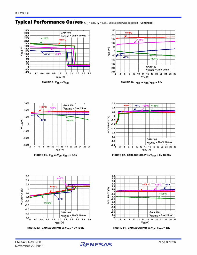
Typical Performance Curves VCC = 12V, RL = 1MΩ, unless otherwise specified.
FIGURE 3. HIGH-SIDE and LOW-SIDE THRESHOLD VOLTAGE VRS+(L-H) and VRS+(H-L), VSENSE = 10mV
FIGURE 4. VOUT vs VRS+, VSENSE = 20mV TRANSIENT RESPONSE
FIGURE 5. LARGE SIGNAL TRANSIENT RESPONSE VRS+ = 0.2V, VSENSE = 100mV
FIGURE 6. LARGE SIGNAL TRANSIENT RESPONSE VRS+ = 12V, VSENSE = 100mV
FIGURE 7. VOS (µV) DISTRIBUTION AT +25°C, VRS+ = 12V, QUANTITY: 100
FIGURE 8. VOS vs VRS+
0
0.2
0.4
0.6
0.8
1.0
1.2
1.4
1.6
1.8
0 0.2 0.4 0.6 0.8 1.0 1.2 1.4 1.6 1.8 2.0TIME (ms)
VO
LT
S (
V)
VTH(L-H) = 1.52V
VTH(H-L) = 1.23V
VRS+
G100, VOUT = 1V
G50, VOUT = 500mVG20, VOUT = 200mV
VOUT (G = 100)
0
0.4
0.8
1.2
1.6
2.0
2.4
0 0.2 0.4 0.6 0.8 1.0 1.2 1.4 1.6 1.8 2.0TIME (ms)
VR
S+ (
V)
0
2
4
6
8
10
12
VO
UT (
V)RL = 1MΩ
VCC = 12V
VRS+
G100, VOUT = 2V
G50, VOUT = 1VG20, VOUT = 400mV
VOUT (G = 100)
0
2
4
6
8
10
12
0 10 20 30 40 50 60 70 80 90 100
TIME (µs)
VO
UT (
V)
GAIN 100
0
2
4
6
8
10
12
0 10 20 30 40 50 60 70 80 90 100TIME (µs)
VO
UT (
V)
GAIN 100
VOS (µV)
UN
ITS
0
2
4
6
8
10
12
14
16
18
20
-250 -200 -150 -100 -50 0 50 100
GAIN 100VSENSE = 20mV, 100mV
0 2 4 6 8 10 12 14 16 18 20 22 24 26 28
VRS+ (V)
VO
S (
µV
)
-400-200
0200400600800
1000120014001600180020002200240026002800
+25°C-40°C
+125°C +100°C
GAIN 100VSENSE = 20mV, 100mV
FN6548 Rev 6.00 Page 7 of 26November 22, 2013
ISL28006
FIGURE 9. VOS vs VRS+ FIGURE 10. VOS vs VCC, VRS+= 12V
FIGURE 11. VOS vs VCC, VRS+ = 0.1V FIGURE 12. GAIN ACCURACY vs VRS+ = 0V TO 28V
FIGURE 13. GAIN ACCURACY vs VRS+ = 0V TO 2V FIGURE 14. GAIN ACCURACY vs VCC, VRS+ = 12V
Typical Performance Curves VCC = 12V, RL = 1MΩ, unless otherwise specified. (Continued)
VRS+ (V)
VO
S (
µV
)
-400-200
0200400600800
1000120014001600180020002200240026002800
0 0.2 0.4 0.6 0.8 1.0 1.2 1.4 1.6 1.8 2.0
+25°C-40°C
+125°C+100°C
GAIN 100VSENSE = 20mV, 100mV
-250
-200
-150
-100
-50
0
50
100
150
200
250
2 4 6 8 10 12 14 16 18 20 22 24 26 28VCC (V)
VO
S (
µV
)
+25°C
-40°C+125°C
+100°C
GAIN 100VSENSE = 2mV, 20mV
-3000
-2000
-1000
0
1000
2000
3000
2 4 6 8 10 12 14 16 18 20 22 24 26 28VCC (V)
VO
S (
µV
) +125°C
+100°C +25°C
-40°C
GAIN 100VSENSE = 2mV, 20mV
0 2 4 6 8 10 12 14 16 18 20 22 24 26 28
AC
CU
RA
CY
(%
)
-1.4
-1.2
-1.0
-0.8
-0.6
-0.4
-0.2
0
0.2
0.4
0.6
VRS+ (V)
+100°C +25°C-40°C +125°C
GAIN 100VSENSE = 20mV, 100mV
VRS+ (V)0 0.2 0.4 0.6 0.8 1.0 1.2 1.4 1.6 1.8 2.0
AC
CU
RA
CY
(%
)
-1.4
-1.2
-1.0
-0.8
-0.6
-0.4
-0.2
0
0.2
0.4
0.6
+100°C
+25°C
-40°C
+125°C
GAIN 100VSENSE = 20mV, 100mV
AC
CU
RA
CY
(%
)
VCC (V)
-5-4.5-4.0-3.5-3.0-2.5-2.0-1.5-1.0-0.5
00.51.01.52.02.53.0
2 4 6 8 10 12 14 16 18 20 22 24 26 28
+100°C +25°C -40°C
+125°C
GAIN 100VSENSE = 2mV, 20mV
FN6548 Rev 6.00 Page 8 of 26November 22, 2013

ISL28006
FIGURE 15. GAIN ACCURACY vs VCC, VRS+ = 0.1V FIGURE 16. NORMALIZED VOA vs IOUT
FIGURE 17. GAIN vs FREQUENCY VRS+ = 100mV/12V, VSENSE = 100mV, VOUT = 50mVP-P
FIGURE 18. VOS (µV) vs TEMPERATURE
FIGURE 19. CAPACITIVE LOAD DRIVE GAIN vs FREQUENCY FIGURE 20. CAPACITIVE LOAD DRIVE PHASE vs FREQUENCY
Typical Performance Curves VCC = 12V, RL = 1MΩ, unless otherwise specified. (Continued)
VCC (V)
AC
CU
RA
CY
(%
)
-20
-18
-16
-14
-12
-10
-8
-6
-4
-2
0
2
2 4 6 8 10 12 14 16 18 20 22 24 26 28
+125°C
+25°C -40°C
+100°C
GAIN 100VSENSE = 2mV, 20mV
1µ 10µ 100µ 1m 10m
IOUT(A)
VO
A P
ER
CE
NT
AC
CU
RA
CY
(%
)
-1.0
-0.9
-0.8
-0.7
-0.6
-0.5
-0.4
-0.3
-0.2
-0.1
0.0
0.1
0.2
+100°C
+25°C
-40°C
+125°C
GAIN 100
10 100 1k 10k 100k 1MFREQUENCY (Hz)
GA
IN (
dB
)
-35
-25
-15
-5
5
15
25
35
45
GAIN 100
VCC = 12V
AV = 100
RL = 1MΩ
VSENSE = 100mV
VRS+ = 12V
VRS+= 100mV
-100
-80
-60
-40
-20
0
20
40
-50 -25 0 25 50 75 100 125TEMPERATURE (°C)
VO
S (
µV
)
GAIN 100VSENSE = 20mV, 100mV
VRS+ = 12V
-40
-30
-20
-10
0
10
20
30
40
1.E+03 1.E+04 1.E+05 1.E+06
FREQUENCY (Hz)
GA
IN (
dB
)
50
VCC = 5V
AV = 100
VOUT = 400mVP-P
VRS- = 3V
NO CL
4.7nF
100pF
1000pF
10nF
-220
-180
-140
-100
-60
-20
20
60
100
140
180
220
1.E+03 1.E+04 1.E+05 1.E+06
FREQUENCY (Hz)
PH
AS
E (
°)
VCC = 5V
AV = 100
VOUT = 400mVP-P
VRS- = 3V
NO CL
4.7nF
100pF 1000pF
10nF
FN6548 Rev 6.00 Page 9 of 26November 22, 2013

ISL28006
FIGURE 21. GAIN ACCURACY (%) vs TEMPERATURE FIGURE 22. VOUT ERROR (%) vs TEMPERATURE
FIGURE 23. VOS (µV) DISTRIBUTION AT +25°C, VRS+ = 12V, QUANTITY: 100
FIGURE 24. VOS vs VRS+
FIGURE 25. VOS vs VRS+ FIGURE 26. VOS vs VCC, VRS+ = 12V
Typical Performance Curves VCC = 12V, RL = 1MΩ, unless otherwise specified. (Continued)
-0.10
-0.05
0
0.05
0.10
0.15
0.20
0.25
0.30
-50 -25 0 25 50 75 100 125
TEMPERATURE (°C)
GA
IN A
CC
UR
AC
Y (
%)
GAIN 100VSENSE = 20mV, 100mV
VRS+ = 12V
-1
-0.9
-0.8
-0.7
-0.6
-0.5
-50 -25 0 25 50 75 100 125
TEMPERATURE (°C)
VO
UT E
RR
OR
(%
)
GAIN 100
VRS+ = 12V
VOS (µV)
UN
ITS
0
2
4
6
8
10
12
14
16
18
20
-250 -200 -150 -100 -50 0 50 100
GAIN 50VSENSE = 20mV, 100mV
0 2 4 6 8 10 12 14 16 18 20 22 24 26 28
VRS+ (V)
VO
S (
µV
)
-400-200
0200400600800
1000120014001600180020002200240026002800
+25°C-40°C
+125°C+100°C
GAIN 50VSENSE = 20mV, 100mV
VRS+ (V)
VO
S (
µV
)
-400-200
0200400600800
1000120014001600180020002200240026002800
0 0.2 0.4 0.6 0.8 1.0 1.2 1.4 1.6 1.8 2.0
+25°C
-40°C
+125°C
+100°C
GAIN 50VSENSE = 20mV, 100mV
-250
-200
-150
-100
-50
0
50
100
150
200
250
2 4 6 8 10 12 14 16 18 20 22 24 26 28VCC (V)
VO
S (
µV
)
+25°C
-40°C
+125°C
+100°C
GAIN 50VSENSE = 2mV, 0mV
FN6548 Rev 6.00 Page 10 of 26November 22, 2013

ISL28006
FIGURE 27. VOS vs VCC, VRS+ = VRS+ = 0.1V FIGURE 28. GAIN ACCURACY vs VRS+ = 0V TO 28V
FIGURE 29. GAIN ACCURACY vs VRS+ = 0V TO 2V FIGURE 30. GAIN ACCURACY vs VCC, HIGH-SIDE
FIGURE 31. GAIN ACCURACY vs VCC, LOW-SIDE FIGURE 32. NORMALIZED VOA vs IOUT
Typical Performance Curves VCC = 12V, RL = 1MΩ, unless otherwise specified. (Continued)
-3000
-2000
-1000
0
1000
2000
3000
2 4 6 8 10 12 14 16 18 20 22 24 26 28VCC (V)
VO
S (
µV
) +125°C
+100°C +25°C
-40°C
GAIN 50VSENSE = 2mV, 0mV
+100°C
+25°C -40°C
+125°C
0 2 4 6 8 10 12 14 16 18 20 22 24 26 28
AC
CU
RA
CY
(%
)
-1.4
-1.2
-1.0
-0.8
-0.6
-0.4
-0.2
0
0.2
0.4
0.6
VRS+ (V)
GAIN 50VSENSE = 20mV, 100mV
VRS+ (V)0 0.2 0.4 0.6 0.8 1.0 1.2 1.4 1.6 1.8 2.0
AC
CU
RA
CY
(%
)
-1.4
-1.2
-1.0
-0.8
-0.6
-0.4
-0.2
0
0.2
0.4
0.6
+100°C
+25°C
-40°C+125°C GAIN 50VSENSE = 20mV, 100mV
AC
CU
RA
CY
(%
)
VCC (V)
-5.0-4.5-4.0-3.5-3.0-2.5-2.0-1.5-1.0-0.5
00.51.01.52.02.53.0
2 4 6 8 10 12 14 16 18 20 22 24 26 28
+100°C +25°C -40°C
+125°C
GAIN 50VSENSE = 2mV, 20mV
VCC (V)
AC
CU
RA
CY
(%
)
-20
-18
-16
-14
-12
-10
-8
-6
-4
-2
0
2
2 4 6 8 10 12 14 16 18 20 22 24 26 28
+125°C
+25°C -40°C
+100°C
GAIN 50VSENSE = 2mV, 20mV
1µ 10µ 100µ 1m 10m
IOUT(A)
VO
A P
ER
CE
NT
AC
CU
RA
CY
(%
)
-1.0
-0.9
-0.8
-0.7
-0.6
-0.5
-0.4
-0.3
-0.2
-0.1
0.0
0.1
0.2
+100°C
+25°C
-40°C
+125°C
GAIN 50
FN6548 Rev 6.00 Page 11 of 26November 22, 2013

ISL28006
FIGURE 33. GAIN vs FREQUENCY VRS+ = 100mV/12V, VSENSE = 100mV, VOUT = 50mVP-P
FIGURE 34. VOS (µV) vs TEMPERATURE
FIGURE 35. CAPACITIVE LOAD DRIVE GAIN vs FREQUENCY FIGURE 36. CAPACITIVE LOAD DRIVE PHASE vs FREQUENCY
FIGURE 37. GAIN ACCURACY (%) vs TEMPERATURE FIGURE 38. VOUT ERROR (%) vs TEMPERATURE
Typical Performance Curves VCC = 12V, RL = 1MΩ, unless otherwise specified. (Continued)
10 100 1k 10k 100k 1MFREQUENCY (Hz)
GA
IN (
dB
)
-35
-25
-15
-5
5
15
25
35
45
VCC = 12V
AV = 50
RL = 1MΩ
VSENSE = 100mV
VRS+ = 12V
VRS+= 100mV
GAIN 50
TEMPERATURE (°C)
VO
S (
µV
)
-230
-210
-190
-170
-150
-130
-110
-90
-70
-50 -25 0 25 50 75 100 125
GAIN 50VSENSE = 20mV, 100mV
VRS+ = 12V
-40
-30
-20
-10
0
10
20
30
40
1.E+03 1.E+04 1.E+05 1.E+06
FREQUENCY (Hz)
GA
IN (
dB
)
50
VCC = 5V
AV = 50
VOUT = 400mVP-P
VRS- = 3V
NO CL
4.7nF 100pF
1000pF
10nF
-220
-180
-140
-100
-60
-20
20
60
100
140
180
220
1.E+03 1.E+04 1.E+05 1.E+06
FREQUENCY (Hz)
PH
AS
E (
°)
VCC = 5V
AV = 50
VOUT = 400mVP-P
VRS- = 3V
NO CL
4.7nF
100pF 1000pF
10nF
-50 -25 0 25 50 75 100 125
TEMPERATURE (°C)
GA
IN A
CC
UR
AC
Y (
%)
0.1
0.11
0.12
0.13
0.14
0.15
0.16
0.17
0.18GAIN 50VSENSE = 20mV, 100mV
VRS+ = 12V
-50 -25 0 25 50 75 100 125
TEMPERATURE (°C)
VO
UT E
RR
OR
(%
)
-0.12
-0.10
-0.08
-0.06
-0.04
-0.02
0
0.02
0.04
0.06
0.08
0.10GAIN 50
VRS+ = 12V
FN6548 Rev 6.00 Page 12 of 26November 22, 2013

ISL28006
FIGURE 39. VOS (µV) DISTRIBUTION AT +25°C, VRS+ = 12V, QUANTITY: 100
FIGURE 40. VOS vs VRS+
FIGURE 41. VOS vs VRS+ FIGURE 42. VOS vs VCC, VRS+ = 12V
FIGURE 43. VOS vs VCC, VRS+ = 0.1V FIGURE 44. GAIN ACCURACY vs VRS+ = 0V TO 28V
Typical Performance Curves VCC = 12V, RL = 1MΩ, unless otherwise specified. (Continued)
VOS (µV)
UN
ITS
0
5
10
15
20
25
30
-250 -200 -150 -100 -50 0 50 100 150
GAIN 20VSENSE = 20mV, 100mV
0 2 4 6 8 10 12 14 16 18 20 22 24 26 28
VRS+ (V)
VO
S (
µV
)
-400-200
0200400600800
1000120014001600180020002200240026002800
+25°C-40°C
+125°C +100°C
GAIN 20VSENSE = 20mV, 100mV
VRS+ (V)
VO
S (
µV
)
-400-200
0200400600800
1000120014001600180020002200240026002800
0 0.2 0.4 0.6 0.8 1 1.2 1.4 1.6 1.8 2
+25°C-40°C
+125°C+100°C
GAIN 20VSENSE = 20mV, 100mV
-250
-200
-150
-100
-50
0
50
100
150
200
250
2 4 6 8 10 12 14 16 18 20 22 24 26 28VCC (V)
VO
S (
µV
)
+25°C
-40°C +125°C
+100°C
GAIN 20VSENSE = 2mV, 20mV
-3000
-2000
-1000
0
1000
2000
3000
2 4 6 8 10 12 14 16 18 20 22 24 26 28VCC (V)
VO
S (
µV
)
+125°C
+100°C +25°C
-40°C
GAIN 20VSENSE = 2mV, 20mV
0 2 4 6 8 10 12 14 16 18 20 22 24 26 28
AC
CU
RA
CY
(%
)
-1.4
-1.2
-1.0
-0.8
-0.6
-0.4
-0.2
0
0.2
0.4
0.6
VRS+ (V)
+100°C
+25°C -40°C
+125°C
GAIN 20VSENSE = 20mV, 100mV
FN6548 Rev 6.00 Page 13 of 26November 22, 2013

ISL28006
FIGURE 45. GAIN ACCURACY vs VRS+ = 0V TO 2V FIGURE 46. GAIN ACCURACY vs VCC, HIGH-SIDE
FIGURE 47. GAIN ACCURACY vs VCC, LOW-SIDE FIGURE 48. NORMALIZED VOA vs IOUT
FIGURE 49. GAIN vs FREQUENCY VRS+ = 100mV/12V, VSENSE = 100mV, VOUT = 50mVP-P
FIGURE 50. VOS (µV) vs TEMPERATURE
Typical Performance Curves VCC = 12V, RL = 1MΩ, unless otherwise specified. (Continued)
VRS+ (V)0 0.2 0.4 0.6 0.8 1.0 1.2 1.4 1.6 1.8 2.0
AC
CU
RA
CY
(%
)
-1.4
-1.2
-1.0
-0.8
-0.6
-0.4
-0.2
0
0.2
0.4
0.6
+100°C
+25°C
-40°C
+125°C
GAIN 20VSENSE = 20mV, 100mV
AC
CU
RA
CY
(%
)
VCC (V)
-5.0-4.5-4.0-3.5-3.0-2.5-2.0-1.5-1.0-0.5
00.51.01.52.02.53.0
2 4 6 8 10 12 14 16 18 20 22 24 26 28
+100°C +25°C -40°C
+125°C
GAIN 20VSENSE = 2mV, 20mV
VCC (V)
AC
CU
RA
CY
(%
)
-20
-18
-16
-14
-12
-10
-8
-6
-4
-2
0
2
2 4 6 8 10 12 14 16 18 20 22 24 26 28
+125°C
-40°C+100°C +25°C
GAIN 20VSENSE = 2mV, 20mV
1µ 10µ 100µ 1m 10m
IOUT(A)
VO
A P
ER
CE
NT
AC
CU
RA
CY
(%
)
-1.0
-0.9
-0.8
-0.7
-0.6
-0.5
-0.4
-0.3
-0.2
-0.1
0.0
0.1
0.2
GAIN 20
+100°C
+25°C
-40°C
+125°C
10 100 1k 10k 100k 1MFREQUENCY (Hz)
GA
IN (
dB
)
-35
-25
-15
-5
5
15
25
35
45
VCC = 12V
AV = 20
RL = 1MΩ
VSENSE = 100mV
VRS+ = 12V
GAIN 20
VRS+ = 100mV
TEMPERATURE (°C)
VO
S (
µV
)
-50 -25 0 25 50 75 100 125-140
-120
-100
-80
-60
-40
-20GAIN 20VSENSE = 20mV, 100mV
VRS+ = 12V
FN6548 Rev 6.00 Page 14 of 26November 22, 2013

ISL28006
FIGURE 51. CAPACITIVE LOAD DRIVE GAIN VS FREQUENCY FIGURE 52. CAPACITIVE LOAD DRIVE PHASE VS FREQUENCY
FIGURE 53. GAIN ACCURACY (%) vs TEMPERATURE FIGURE 54. VOUT ERROR (%) vs TEMPERATURE
FIGURE 55. VOS (µV) DISTRIBUTION AT +25°C, VRS+ = 12V, QUANTITY: 100
FIGURE 56. VOS vs VRS+
Typical Performance Curves VCC = 12V, RL = 1MΩ, unless otherwise specified. (Continued)
-40
-30
-20
-10
0
10
20
30
40
1.E+03 1.E+04 1.E+05 1.E+06
FREQUENCY (Hz)
GA
IN (
dB
)
VCC = 5V
AV = 20
VOUT = 400mVP-P
VRS- = 3V
NO CL
4.7nF 100pF
1000pF
10nF
-220
-180
-140
-100
-60
-20
20
60
100
140
180
220
1.E+03 1.E+04 1.E+05 1.E+06
FREQUENCY (Hz)
PH
AS
E (
°)
VCC = 5V
AV = 20
VOUT = 400mVP-P
VRS- = 3V
NO CL
4.7nF
100pF 1000pF
10nF
0.290
0.295
0.300
0.305
0.310
0.3150
0.320
0.325
0.330
-50 -25 0 25 50 75 100 125
TEMPERATURE (°C)
GA
IN A
CC
UR
AC
Y (
%)
GAIN 20VSENSE = 20mV, 100mV
VRS+ = 12V
-50 -25 0 25 50 75 100 125
TEMPERATURE (°C)
VO
UT E
RR
OR
(%
)
0.15
0.17
0.19
0.21
0.23
0.25
0.27
0.29
0.31GAIN 20VRS+ = 12V
-200 -160 -120 -80 -40 0 40 80 120 160 200
VOS (µV)
UN
ITS
0
2
4
6
8
10
12
14
16
18
20
22
24
26GAIN 101 ADJRf = 100k, Rg = 1k
VSENSE = 20mV, 100mV
0 2 4 6 8 10 12 14 16 18 20 22 24 26 28
VRS+ (V)
VO
S (
µV
)
-400-200
0200400600800
1000120014001600180020002200240026002800
+25°C-40°C
+125°C +100°C
GAIN 101 ADJ
Rf = 100k, Rg = 1k
VSENSE = 20mV, 100mV
FN6548 Rev 6.00 Page 15 of 26November 22, 2013

ISL28006
FIGURE 57. VOS vs VRS+ FIGURE 58. VOS vs VCC, HIGH-SIDE
FIGURE 59. VOS vs VCC, LOW-SIDE FIGURE 60. GAIN ACCURACY vs VRS+ = 0V TO 28V
FIGURE 61. GAIN ACCURACY vs VRS+ = 0V TO 2V FIGURE 62. GAIN ACCURACY vs VCC, VRS+ = 12V
Typical Performance Curves VCC = 12V, RL = 1MΩ, unless otherwise specified. (Continued)
VRS+ (V)
VO
S (
µV
)
-400-200
0200400600800
1000120014001600180020002200240026002800
0 0.2 0.4 0.6 0.8 1.0 1.2 1.4 1.6 1.8 2.0
+25°C-40°C
+125°C
+100°C
GAIN 101 ADJRf = 100k, Rg = 1k
VSENSE = 20mV, 100mV
-250
-200
-150
-100
-50
0
50
100
150
200
250
2 4 6 8 10 12 14 16 18 20 22 24 26 28VCC (V)
VO
S (
µV
)
+25°C
-40°C
+125°C
+100°C
GAIN 101 ADJRf = 100k, Rg = 1kVSENSE = 2mV, 20mV
-3000
-2000
-1000
0
1000
2000
3000
2 4 6 8 10 12 14 16 18 20 22 24 26 28VCC (V)
VO
S (
µV
)
+125°C
+100°C +25°C
-40°C
GAIN 101 ADJRf = 100k, Rg = 1kVSENSE = 2mV, 20mV
0 2 4 6 8 10 12 14 16 18 20 22 24 26 28
AC
CU
RA
CY
(%
)
-1.4
-1.2
-1.0
-0.8
-0.6
-0.4
-0.2
0
0.2
0.4
0.6
+100°C
+25°C-40°C
+125°C
VRS+ (V)
GAIN 101 ADJRf = 100k, Rg = 1kVSENSE = 20mV, 100mV
VRS+ (V)0 0.2 0.4 0.6 0.8 1.0 1.2 1.4 1.6 1.8 2.0
AC
CU
RA
CY
(%
)
-1.4
-1.2
-1.0
-0.8
-0.6
-0.4
-0.2
0
0.2
0.4
0.6
+100°C
+25°C -40°C
+125°C
GAIN 101 ADJRf = 100k, Rg = 1kVSENSE = 20mV, 100mV
AC
CU
RA
CY
(%
)
VCC (V)
-5.0-4.5-4.0-3.5-3.0-2.5-2.0-1.5-1.0-0.5
00.51.01.52.02.53.0
2 4 6 8 10 12 14 16 18 20 22 24 26 28
+100°C+25°C
-40°C
+125°C
GAIN 101 ADJRf = 100k, Rg = 1kVSENSE = 2mV, 20mV
FN6548 Rev 6.00 Page 16 of 26November 22, 2013

ISL28006
FIGURE 63. GAIN ACCURACY vs VCC, VRS+ = 0.1V FIGURE 64. NORMALIZED VOA vs IOUT
FIGURE 65. GAIN vs FREQUENCY VRS+ = 100mV/12V, VSENSE = 100mV, VOUT = 50mVP-P
FIGURE 66. VOS (µV) vs TEMPERATURE
FIGURE 67. GAIN ACCURACY (%) vs TEMPERATURE FIGURE 68. VOUT ERROR (%) vs TEMPERATURE
Typical Performance Curves VCC = 12V, RL = 1MΩ, unless otherwise specified. (Continued)
VCC (V)
AC
CU
RA
CY
(%
)
-20
-18
-16
-14
-12
-10
-8
-6
-4
-2
0
2
2 4 6 8 10 12 14 16 18 20 22 24 26 28
+125°C
+100°C +25°C -40°C
GAIN 101 ADJRf = 100k, Rg = 1kVSENSE = 2mV, 20mV
-1.0
-0.8
-0.6
-0.4
-0.2
0.00.2
1µ 10µ 100µ 1m 10mIOUT(A)
VO
A P
ER
CE
NT
AC
CU
RA
CY
(%
)
-1.0
-0.8
-0.6
-0.4
-0.2
0.00.2
+100°C
-40°C
GAIN 21 ADJRf = 100kRg = 5k
+125°C
GAIN 101 ADJRf = 100kRg = 1k
+25°C
+100°C
-40°C
+125°C
+25°C
100 1k 10k 100k 1MFREQUENCY (Hz)
GA
IN (
dB
)
0
5
10
15
20
25
30
35
40
45
VCC = 12V
GAIN = 21, 51, 101
RL = 1MΩ
VSENSE = 100mV
Rf = 100kRg = 1k, 2k, 5k
VRS+ = 12V GAIN = 21
VRS+ = 0.1V GAIN = 101
VRS+ = 12V GAIN = 51
VRS+ = 0.1V GAIN = 21
VRS+ = 12V GAIN = 51
VRS+ = 12V GAIN = 101
TEMPERATURE (°C)
VO
S (
µV
)
-50 -25 0 25 50 75 100 125-350
-300
-250
-200
-150
-100
-50
0
50
100
150
200
VRS+ = 12V
GAIN = 21, 101
RL = 1MΩ
VSENSE = 20mV, 100mV
Rf = 100kRg = 1k, 5k
GAIN = 21
GAIN = 101
0
0.05
0.10
0.15
0.20
0.25
0.30
0.35
0.40
-50 -25 0 25 50 75 100 125
TEMPERATURE (°C)
GA
IN A
CC
UR
AC
Y (
%)
VRS+ = 12V
GAIN = 21, 101
RL = 1MΩ
VSENSE = 20mV, 100mV
Rf = 100kRg = 1k, 5k
GAIN = 21
GAIN = 101
-50 -25 0 25 50 75 100 125
TEMPERATURE (°C)
VO
UT E
RR
OR
(%
)
-0.2
-0.1
0
0.1
0.2
0.3
0.4
0.5
0.6
VRS+ = 12V
GAIN = 21, 101
RL = 1MΩ
VSENSE = 20mV, 100mV
Rf = 100kRg = 1k, 5k
GAIN = 21
GAIN = 101
FN6548 Rev 6.00 Page 17 of 26November 22, 2013

ISL28006
FIGURE 69. LOW SIDE CURRENT SENSING INPUT BIAS CURRENTS FIGURE 70. HIGH SIDE CURRENT SENSING INPUT BIAS CURRENTS
Typical Performance Curves VCC = 12V, RL = 1MΩ, unless otherwise specified. (Continued)
-15
-10
-5
0
5
10
15
0 50 100 150 200 250
DIFFERENTIAL VOLTAGE RS+ TO RS- (mV)
INP
UT
BIA
S C
UR
RE
NT
(µ
A)
VCC = 12V
AV = 20
RL = 1M
VRS- = 0V
IRS+
IRS+ -5
0
5
10
15
20
0 50 100 150 200 250
DIFFERENTIAL VOLTAGE RS+ TO RS- (mV)
-10
INP
UT
BIA
S C
UR
RE
NT
(µ
A)
VCC = 12V
AV = 20
RL = 1M
VRS- = 12V
IRS+
IRS+
Test Circuits and Waveforms
FIGURE 71. ICC, VOS, VOA, CMRR, PSRR, GAIN ACCURACY FIGURE 72. INPUT BIAS CURRENT, LEAKAGE CURRENT
FIGURE 73. ts, SATURATION RECOVERY TIME FIGURE 74. GAIN vs FREQUENCY
FIGURE 75. SLEW RATE
RS+
VCC
RS-
VOUT
OUT
RLGND
VSENSE VRS+
1MΩ
+
-
+
-
ICC
RS+
VCC
RS-
VOUT
OUT
RLGND
VSENSEVRS+
1MΩ
+
-
+
-
R1
R2
VR1
VR2
RS+
VCC
RS-
VOUT
OUT
RL
GND
VRS-
VRS+
1MΩ
PULSE GENERATOR
RS+
VCC
RS-
VOUT
OUT
RL
GND
VSENSEVRS+
1MΩ
SIGNALGENERATOR
RS+
VCC
RS-
VOUT
OUT
RL
GNDVRS+
1MΩ
PULSEGENERATOR
FN6548 Rev 6.00 Page 18 of 26November 22, 2013

ISL28006
Applications Information
Functional DescriptionThe ISL28006-20, ISL28006-50 and ISL28006-100 are single supply, uni-directional current sense amplifiers with fixed gains of 20V/V, 50V/V and 100V/V respectively. The ISL28006-ADJ is single supply, uni-directional current sense amplifier with an adjustable gain via external resistors (see Figure 80). The ISL28006-ADJ is stable for gains of 20 and higher.
The ISL28006 is a 2-stage amplifier. Figure 76 shows the active circuitry for high-side current sense applications where the sense voltage is between 1.35V to 28V. Figure 77 shows the active circuitry for ground sense applications where the sense voltage is between 0V to 1.35V.
The first stage is a bi-level trans-conductance amp and level translator. The gm stage converts the low voltage drop (VSENSE) sensed across an external milli-ohm sense resistor, to a current (@ gm = 21.3µA/V). The trans-conductance amplifier forces a current through R1 resulting to a voltage drop across R1 that is equal to the sense voltage (VSENSE). The current through R1 is mirrored across R5 creating a ground-referenced voltage at the input of the second amplifier equal to VSENSE.
The second stage is responsible for the overall gain and frequency response performance of the device. The fixed gains (20, 50, 100) are set with internal resistors Rf and Rg. The variable gain (ADJ) has an additional FB pin and uses external
gain resistors to set the gain of the output. For the fixed gain amps the only external component needed is a current sense resistor (typically 0.001Ω to 0.01Ω, 1W to 2W).
The transfer function for the fixed gain parts is given in Equation 1.
The transfer function for the adjustable gain part is given in Equation 2.
Where ISRS is the product of the load current and the sense resistor and is equal to VSENSE.
When the sensed input voltage is >1.35V, the gmHI amplifier path is selected and the input gm stage derives its ~2.86µA supply current from the input source through the RS+ terminal. When the sense voltage at RS+ drops below the 1.35V threshold, the gmLO amplifier is enabled for Low Side current sensing. The gmLO input bias current reverses, flowing out of the RS- pin. Since the gmLO amplifier is sensing voltage around ground, it cannot source current to R5. A current mirror referenced off Vcc supplies the current to the second stage for generating a ground referenced output voltage. See Figures 69 and 70 for typical input bias currents for High and Low side current sensing.
VOUT GAIN ISRS VOS+ = (EQ. 1)
VOUT 1RFRG-------+
ISRS VOS+ = (EQ. 2)
FIGURE 76. HIGH-SIDE CURRENT DETECTION
RS+
RS-
gmHI
gmLO
RS
IS
+
-
LOAD
VSENSE
1.35V
IMIRROR
+
-OUT
Rf
Rg
R1
R5
VCC
HIGH-SIDESENSING
OPTIONALTRANSIENTPROTECTION
OPTIONALFILTERCAPACITOR
‘VSENSE
VCC = 2V to 28V
R2
R3
R4
I = 2.86µA
GND
VSENSE VRS+ = 2V TO 28V
FN6548 Rev 6.00 Page 19 of 26November 22, 2013

ISL28006
FIGURE 77. LOW-SIDE CURRENT DETECTION
RS-
gmHI
gmLO
RS
IS
+
-
LOAD
VSENSE
1.35V
+
-OUT
Rf
Rg
R1
R5
VCC
LOW-SIDESENSING
OPTIONALTRANSIENTPROTECTION
OPTIONALFILTERCAPACITOR
VSENSE
VCC = 2V TO 28V
R2
R3
R4
I = 2.86µA
VCC
GND
VSENSE VRS+= 0V TO 28V
RS+
IMIRROR
FN6548 Rev 6.00 Page 20 of 26November 22, 2013
ISL28006
Hysteretic ComparatorThe input trans-conductance amps are under control of a hysteretic comparator operating from the incoming source voltage on the RS+ pin (Figure 78). The comparator monitors the voltage on RS+ and switches the sense amplifier from the low-side gm amp to the high-side gm amplifier whenever the input voltage at RS+ increases above the 1.35V threshold. Conversely, a decreasing voltage on the RS+ pin, causes the hysteric comparator to switch from the high-side gm amp to the low-side gm amp as the voltage decreases below 1.35V. It is that low-side sense gm amplifier that gives the ISL28006 the proprietary ability to sense current all the way to 0V. Negative voltages on the RS+ or RS- are beyond the sensing voltage range of this amplifier.
Typical Application CircuitFigure 80 shows the basic application circuit and optional protection components for switched-load applications. For applications where the load and the power source is permanently connected, only an external sense resistor is needed. For applications where fast transients are caused by hot plugging the source or load, external protection components may be needed. The external current limiting resistor (RP) in Figure 80 may be required to limit the peak current through the internal ESD diodes to <20mA. This condition can occur in applications that experience high levels of in-rush current causing high peak voltages that can damage the internal ESD diodes. An RP resistor
value of 100Ω will provide protection for a 2V transient with the maximum of 20mA flowing through the input while adding only an additional 13µV (worse case over-temperature) of VOS. Refer to Equation 3:
Switching applications can generate voltage spikes that can overdrive the amplifier input and drive the output of the amplifier into the rails, resulting in a long overload recover time. Capacitors CM and CD filter the common mode and differential voltage spikes.
Error SourcesThere are 3 dominant error sources: gain error, input offset voltage error and Kelvin voltage error (see Figure 79). The gain error is dominated by the internal resistance matching tolerances. The remaining errors appear as sense voltage errors at the input to the amplifier. They are VOS of the amplifier and Kelvin voltage errors. If the transient protection resistor is added, an additional VOS error can result from the IxR voltage due to input bias current. The limiting resistor should only be added to the RS- input, due to the high-side gm amplifier (gmHI) sinking several micro amps of current through the RS+ pin.
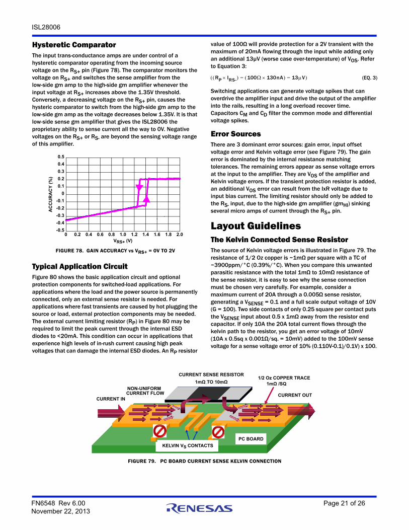
Layout GuidelinesThe Kelvin Connected Sense ResistorThe source of Kelvin voltage errors is illustrated in Figure 79. The resistance of 1/2 Oz copper is ~1mΩ per square with a TC of ~3900ppm/°C (0.39%/°C). When you compare this unwanted parasitic resistance with the total 1mΩ to 10mΩ resistance of the sense resistor, it is easy to see why the sense connection must be chosen very carefully. For example, consider a maximum current of 20A through a 0.005Ωsense resistor, generating a VSENSE = 0.1 and a full scale output voltage of 10V (G = 100). Two side contacts of only 0.25 square per contact puts the VSENSE input about 0.5 x 1mΩ away from the resistor end capacitor. If only 10A the 20A total current flows through the kelvin path to the resistor, you get an error voltage of 10mV (10A x 0.5sq x 0.001Ω/sq. = 10mV) added to the 100mV sense voltage for a sense voltage error of 10% (0.110V-0.1)/0.1V) x 100.
FIGURE 78. GAIN ACCURACY vs VRS+ = 0V TO 2V
VRS+ (V)
-0.5
-0.4
-0.3
-0.2
-0.1
0
0.1
0.2
0.3
0.4
0.5
0 0.2 0.4 0.6 0.8 1.0 1.2 1.4 1.6 1.8 2.0
AC
CU
RA
CY
(%
)
(EQ. 3)RP IRS- 100 130nA 13V= =
FIGURE 79. PC BOARD CURRENT SENSE KELVIN CONNECTION
PC Board
Non-uniformCurrent Flow
Current Sense Resistor1 to 10mO
Current In Current Out
Kelvin VS Contacts
Copper Trace30mO/Sq.
PC Board
Non-uniformCurrent Flow
Current Sense Resistor1 to 10mO
Current In Current Out
Kelvin VS Contacts
Copper Trace30mO/Sq.
CURRENT SENSE RESISTOR
1mΩ TO 10mΩ 1mΩ /SQ
CURRENT OUT CURRENT IN
NON-UNIFORMCURRENT FLOW
PC BOARD
KELVIN VS CONTACTS
1/2 Oz COPPER TRACE
FN6548 Rev 6.00 Page 21 of 26November 22, 2013

ISL28006
Overall Accuracy (VOA %)VOA is defined as the total output accuracy Referred-to-Output (RTO). The output accuracy contains all offset and gain errors, at a single output voltage. Equation 4 is used to calculate the % total output accuracy.
whereVOUT Actual = VSENSE x GAINExample: Gain = 100, For 100mV VSENSE input we measure 10.1V. The overall accuracy (VOA) is 1% as shown in Equation 5.
Power DissipationIt is possible to exceed the +150°C maximum junction temperatures under certain load and power supply conditions. It is therefore important to calculate the maximum junction temperature (TJMAX) for all applications to determine if power supply voltages, load conditions, or package type need to be modified to remain in the safe operating area. These parameters are related using Equation 6:
where:
• PDMAXTOTAL is the sum of the maximum power dissipation of each amplifier in the package (PDMAX)
• PDMAX for each amplifier can be calculated using Equation 7:
where:
• TMAX = Maximum ambient temperature
• JA = Thermal resistance of the package
• PDMAX = Maximum power dissipation of 1 amplifier
• VCC = Total supply voltage
• IqMAX = Maximum quiescent supply current of 1 amplifier
• VOUTMAX = Maximum output voltage swing of the application
• RL = Load resistance
FIGURE 80. TYPICAL APPLICATION CIRCUIT
gmHI
gmLO
1.35V
+
-
VCC
ADJOPTIONONLY
I = 2.86µA
GND
RS
RS-
RP
(1mΩTO
0.1Ω)
0.1VDC TO
28VDC
+
-
CD
LOAD
CM
2.7VDC TO
28VDC
RS+
FB
OUT
FIXED GAINOPTIONONLY
VOA 100VOUTactual VOUT ectedexp–
VOUT ectedexp------------------------------------------------------------------------------
= (EQ. 4)
(EQ. 5)VOA 10010.1 10–
10------------------------- 1%= =
TJMAX TMAX JAxPDMAXTOTAL+= (EQ. 6)
PDMAX VS IqMAX VS - VOUTMAX VOUTMAX
RL------------------------+= (EQ. 7)
FN6548 Rev 6.00 Page 22 of 26November 22, 2013

ISL28006
Revision HistoryThe revision history provided is for informational purposes only and is believed to be accurate, but not warranted. Please go to web to make sure you have the latest Rev.
DATE REVISION CHANGE
November 22, 2013 FN6548.6 Added eight new Typical Performance Curves1. Av=100 Capacitive Load Drive Gain vs Freq2. Av=100 Capacitive Load Drive Phase vs Freq3. Av=50 Capacitive Load Drive Gain vs Freq4. Av=50 Capacitive Load Drive Phase vs Freq5. Av=20 Capacitive Load Drive Gain vs Freq6. Av=20 Capacitive Load Drive Phase vs Freq7. High Side Operation Input Bias Currents8. Low Side Operation Input Bias Currents
Under Electrical Specifications Table:Changed parameter from Is to Icc to clarify supply currentOrdering information table on page 3: Changed Note 4 location in the table.
April 12, 2011 FN6548.5 Converted to new templatePage 1 - Changed headings for “Typical Application” and “Gain Accuracy vs VRS+ = 0V to 28V” to Figure titles (Figures 1 and 2).Page 1 - Updated Intersil Trademark statement at bottom of page 1 per directive from Legal.Page 7 - Updated over temp note in Min Max column of spec tables from "Parameters with MIN and/or MAX limits are 100% tested at +25°C, unless otherwise specified. Temperature limits established by characterization and are not production tested." to new standard "Compliance to datasheet limits is assured by one or more methods: production test, characterization and/or design." Page 19 - Figure 69, Low side current detection schematic: Moved the LOAD from the ground side of the power side circuit to the high side.
September 2, 2010 FN6548.4 Added -T7A tape and reel options to Ordering Information Table for all packages.
May 12, 2010 FN6548.3 Added Note 4 to Part Marking Column in “Ordering Information” on page 3.Corrected hyperlinks in Notes 1 and 3 in “Ordering Information” on page 3.
April 8, 2010 Removed “Coming Soon” from evaluation boards in “Ordering Information” on page 3.
April 7, 2010 Added “Related Literature” on page 1Updated Package Drawing Number in the “Ordering Information” on page 3 for the 20V, 50V and 100V options from MDP0038 to P50.64A.Revised package outline drawing from MDP0038 to P5.064A on page 24. MDP0038 package contained 2 packages for both the 5 and 6 Ld SOT-23. MDP0038 was obsoleted and the packages were separated and made into 2 separate package outline drawings; P5.064A and P6.064A. Changes to the 5 Ld SOT-23 were to move dimensions from table onto drawing, add land pattern and add JEDEC reference number.
March 10, 2010 FN6548.2 Releasing adjustable gain option.Added adjustable block diagram (Page 2), Added adjustable gain limits to electrical spec table, added Figures 47 through 60, Added +85°C curves to Figures 6 thru 14, 20 thru 28, 34 thru 42, and Figures 48 thru 56. Modified Figure 70.
February 4, 2010 FN6548.1 -Page 1:Edited last sentence of paragraph 2.Moved order of GAIN listings from 20, 50, 100 to 100, 50, 20 in the 3rd paragraph.Under Features ....removed "Low Input Offset Voltage 250µV, max"Under Features .... moved order of parts listing from 20, 50, 100 (from top to bottom) to 100, 50, 20.-Page 3: Removed coming soon on ISL28006FH50Z and ISL28006FH20Z and changes the order or listing them to 100, 50, 20.-Page 5: VOA test. Under conditions column ...deleted 20mV to. It now reads ... Vsense = 100mV SR test. Under conditions column ..deleted what was there. It now reads ... Pulse on RS+pin, See Figure 51-Page 6: ts test. Removed Gain = 100 and Gain = 100V/V in both description and conditions columns respectively.-Page 9: Added VRS+= 12V to Figures 16, 17, 18. -Page 11: Added VRS+= 12V to Figures 30, 31, 32. -Page 13 & 14: Added VRS+= 12V to Figures 44, 45, 46. -Page 14 Added Figure 51 and adjusted figure numbers to account for the added figure.-Figs 8, 26, and 40 change "HIGH SIDE" to "VRS = 12V", where RS is subscript.-Figs 9, 27, and 41 change "LOW SIDE" to "VRS = 0.1V", where RS is subscript.
December 14, 2009 FN6548.0 Initial Release
FN6548 Rev 6.00 Page 23 of 26November 22, 2013

ISL28006
Intersil products are manufactured, assembled and tested utilizing ISO9001 quality systems as notedin the quality certifications found at www.intersil.com/en/support/qualandreliability.html
Intersil products are sold by description only. Intersil may modify the circuit design and/or specifications of products at any time without notice, provided that such modification does not, in Intersil's sole judgment, affect the form, fit or function of the product. Accordingly, the reader is cautioned to verify that datasheets are current before placing orders. Information furnished by Intersil is believed to be accurate and reliable. However, no responsibility is assumed by Intersil or its subsidiaries for its use; nor for any infringements of patents or other rights of third parties which may result from its use. No license is granted by implication or otherwise under any patent or patent rights of Intersil or its subsidiaries.
For information regarding Intersil Corporation and its products, see www.intersil.com
For additional products, see www.intersil.com/en/products.html
© Copyright Intersil Americas LLC 2009-2013. All Rights Reserved.All trademarks and registered trademarks are the property of their respective owners.
About IntersilIntersil Corporation is a leader in the design and manufacture of high-performance analog, mixed-signal and power management semiconductors. The company's products address some of the largest markets within the industrial and infrastructure, personal computing and high-end consumer markets. For more information about Intersil, visit our website at www.intersil.com.
For the most updated datasheet, application notes, related documentation and related parts, please see the respective product information page found at www.intersil.com. You may report errors or suggestions for improving this datasheet by visiting www.intersil.com/en/support/ask-an-expert.html. Reliability reports are also available from our website at http://www.intersil.com/en/support/qualandreliability.html#reliability
FN6548 Rev 6.00 Page 24 of 26November 22, 2013

ISL28006
FN6548 Rev 6.00 Page 25 of 26November 22, 2013
Package Outline Drawing
P5.064A5 LEAD SMALL OUTLINE TRANSISTOR PLASTIC PACKAGERev 0, 2/10
Dimension is exclusive of mold flash, protrusions or gate burrs.
This dimension is measured at Datum “H”.
Package conforms to JEDEC MO-178AA.
Foot length is measured at reference to guage plane.
Dimensions in ( ) for Reference Only.
Dimensioning and tolerancing conform to ASME Y14.5M-1994.
6.
3.
5.
4.
2.
Dimensions are in millimeters.1.
NOTES:
DETAIL "X"
SIDE VIEW
TYPICAL RECOMMENDED LAND PATTERN
TOP VIEW
INDEX AREAPIN 1
SEATING PLANE
GAUGE
0.45±0.1
(2 PLCS)10° TYP
4
1.90
0.40 ±0.05
2.90
0.95
1.60
2.80
0.05-0.15
1.14 ±0.15
0.20 C A-B DM
(1.20)
(0.60)
(0.95)
(2.40)
0.10 C
0.08-0.20
SEE DETAIL X
1.45 MAX
(0.60)
0-3°
C
B
A
D
3
3
3
0.20 C
(1.90)
2x
0.15 C2x
D
0.15 C2x
A-B
(0.25)
H
5
2
4
5
5
END VIEW
PLANE

ISL28006
FN6548 Rev 6.00 Page 26 of 26November 22, 2013
Package Outline Drawing
P6.0646 LEAD SMALL OUTLINE TRANSISTOR PLASTIC PACKAGERev 4, 2/10
Dimension is exclusive of mold flash, protrusions or gate burrs.
Package conforms to JEDEC MO-178AB.
Foot length is measured at reference to guage plane.
Dimensions in ( ) for Reference Only.
Dimensioning and tolerancing conform to ASME Y14.5M-1994.
5.
3.
4.
2.
Dimensions are in millimeters.1.
NOTES:
DETAIL "X"SIDE VIEW
TYPICAL RECOMMENDED LAND PATTERN
TOP VIEW
END VIEW
INDEX AREAPIN 1
SEATING PLANE
GAUGE
0.45±0.1
(2 PLCS)10° TYP
4
1.90
0.40 ±0.10
2.90 ±0.10
0.95
1.60 +0.15/-0.102.80
0.00-0.15
1.15 +0.15/-0.25
0.20 C A-B DM
(1.20)
(0.60)
(0.95)
(2.40)
0.10 C
0.08-0.22
SEE DETAIL X
(0.25)1.45 MAX
(0.60)
0-8°
C
B
A
D
3
3
3
3
0.20 C2x
1 2 3
6 5 4
PLANE
Related Documents