The Patent Office Journal No. 41/2017 Dated 13/10/2017 36374 CONTINUED FROM PART- 2 (12) PATENT APPLICATION PUBLICATION (21) Application No.201738028168 A (19) INDIA (22) Date of filing of Application :08/08/2017 (43) Publication Date : 13/10/2017 (54) Title of the invention : A COMMUNICATION TERMINAL (51) International classification :H04L1/00 (31) Priority Document No :07016131.0 (32) Priority Date :16/08/2007 (33) Name of priority country :EUROPEAN UNION (86) International Application No Filing Date :PCT/EP2008/004684 :11/06/2008 (87) International Publication No :WO/2009/021572 (61) Patent of Addition to Application Number Filing Date :NA :NA (62) Divisional to Application Number Filed on :557/KOLNP/2010 :12/02/2010 (71)Name of Applicant : 1)PANASONIC CORPORATION Address of Applicant :1006, OAZA KADOMA, KADOMA- SHI, OSAKA 571-8501 JAPAN Japan (72)Name of Inventor : 1)FEUERS„NGER, Martin 2)LÖHR, Joachim 3)GOLITSCHEK EDLER VON ELBWART, Alexander (57) Abstract : The present invention describes a method for configuring a measurement report type to be used by a receiver to report a measurement to a transmitter, wherein the measurement is reported to the transmitter in a report signal over a control channel, said method comprising selecting a first measurement report type and at least one second measurement report type to be used by the receiver to report the measurement, generating a measurement reporting pattern defining an occurrence of the first measurement report type and the at least one second measurement report type in the report signal transmitted by the receiver to the transmitter over control channel, and notifying the first measurement report type, the at least one second measurement report type, and the generated measurement reporting pattern to the receiver. No. of Pages : 25 No. of Claims : 8

Welcome message from author
This document is posted to help you gain knowledge. Please leave a comment to let me know what you think about it! Share it to your friends and learn new things together.
Transcript
The Patent Office Journal No. 41/2017 Dated 13/10/2017 36374
CONTINUED FROM PART- 2 (12) PATENT APPLICATION PUBLICATION (21) Application No.201738028168 A
(19) INDIA
(22) Date of filing of Application :08/08/2017 (43) Publication Date : 13/10/2017
(54) Title of the invention : A COMMUNICATION TERMINAL
(51) International classification :H04L1/00
(31) Priority Document No :07016131.0
(32) Priority Date :16/08/2007
(33) Name of priority country :EUROPEAN
UNION
(86) International Application No
Filing Date
:PCT/EP2008/004684
:11/06/2008
(87) International Publication No :WO/2009/021572
(61) Patent of Addition to Application
Number
Filing Date
:NA
:NA
(62) Divisional to Application Number
Filed on
:557/KOLNP/2010
:12/02/2010
(71)Name of Applicant :
1)PANASONIC CORPORATION Address of Applicant :1006, OAZA KADOMA, KADOMA-
SHI, OSAKA 571-8501 JAPAN Japan
(72)Name of Inventor :
1)FEUERS„NGER, Martin
2)LÖHR, Joachim
3)GOLITSCHEK EDLER VON ELBWART, Alexander
(57) Abstract :
The present invention describes a method for configuring a measurement report type to be used by a receiver to report a measurement
to a transmitter, wherein the measurement is reported to the transmitter in a report signal over a control channel, said method
comprising selecting a first measurement report type and at least one second measurement report type to be used by the receiver to
report the measurement, generating a measurement reporting pattern defining an occurrence of the first measurement report type and
the at least one second measurement report type in the report signal transmitted by the receiver to the transmitter over control channel,
and notifying the first measurement report type, the at least one second measurement report type, and the generated measurement
reporting pattern to the receiver.
No. of Pages : 25 No. of Claims : 8
The Patent Office Journal No. 41/2017 Dated 13/10/2017 36375
(12) PATENT APPLICATION PUBLICATION (21) Application No.201737032671 A
(19) INDIA
(22) Date of filing of Application :14/09/2017 (43) Publication Date : 13/10/2017
(54) Title of the invention : NEUTRALIZING ANTIBODIES TO GP120 AND THEIR USE
(51) International classification :C07K16/10,A61P31/18
(31) Priority Document No :62/136228
(32) Priority Date :20/03/2015
(33) Name of priority country :U.S.A.
(86) International Application No
Filing Date
:PCT/US2016/023145
:18/03/2016
(87) International Publication No :WO 2016/154003
(61) Patent of Addition to Application
Number
Filing Date
:NA
:NA
(62) Divisional to Application Number
Filing Date
:NA
:NA
(71)Name of Applicant :
1)THE UNITED STATES OF AMERICA AS
REPRESENTED BY THE SECRETARY DEPARTMENT
OF HEALTH AND HUMAN SERVICES Address of Applicant :National Institutes of Health Office of
Technology Transfer 6011 Executive Boulevard Suite 325 MSC
7660 Bethesda MD 20852 7660 U.S.A.
(72)Name of Inventor :
1)CONNORS Mark
2)HUANG Jinghe
3)KANG Byong Ha
4)MASCOLA John
5)ISHIDA Elise
6)ZHOU Tongqing
7)KWONG Peter
8)ZHENG Anqi
(57) Abstract :
Antibodies and antigen binding fragments that specifically bind to gp120 and neutralize HIV 1 are disclosed. Nucleic acids encoding
these antibodies vectors and host cells are also provided. Methods for detecting HIV 1 using these antibodies are disclosed. In
addition the use of these antibodies antigen binding fragment nucleic acids and vectors to prevent and/or treat an HIV 1 infection is
disclosed.
No. of Pages : 97 No. of Claims : 50
The Patent Office Journal No. 41/2017 Dated 13/10/2017 36376
(12) PATENT APPLICATION PUBLICATION (21) Application No.201737032724 A
(19) INDIA
(22) Date of filing of Application :15/09/2017 (43) Publication Date : 13/10/2017
(54) Title of the invention : BASE STATION TERMINAL WIRELESS COMMUNICATION SYSTEM BASE STATION
CONTROL METHOD AND TERMINAL CONTROL METHOD
(51) International
classification :H04W72/04,H04W16/14,H04W72/12
(31) Priority Document No :NA
(32) Priority Date :NA
(33) Name of priority
country :NA
(86) International
Application No
Filing Date
:PCT/JP2015/060770
:06/04/2015
(87) International
Publication No :WO 2016/162929
(61) Patent of Addition to
Application Number
Filing Date
:NA
:NA
(62) Divisional to
Application Number
Filing Date
:NA
:NA
(71)Name of Applicant :
1)FUJITSU LIMITED Address of Applicant :1 1 Kamikodanaka 4 chome Nakahara
ku Kawasaki shi Kanagawa 2118588 Japan
(72)Name of Inventor :
1)TANAKA Yoshinori
(57) Abstract :
According to one embodiment a base station (20) has a licensed band transmission unit (220) a determination unit (205) and an
unlicensed band transmission unit (210). The licensed band transmission unit (220) transmits to a terminal a control signal that
designates a shared bandwidth resource that is to be used for data transmission by the terminal. The determination unit (205)
determines whether the shared bandwidth resource is idle or busy. When the determination unit (205) has determined that the shared
bandwidth resource is idle the unlicensed band transmission unit (210) transmits a permission signal that permits transmission over the
shared bandwidth. The control signal or the permission signal includes an offset that on the basis of the permission signal transmitted
from the unlicensed band transmission unit (210) indicates the amount of time between the permission signal and the beginning of
data transmission by the terminal to the base station (20).
No. of Pages : 40 No. of Claims : 13
The Patent Office Journal No. 41/2017 Dated 13/10/2017 36377
(12) PATENT APPLICATION PUBLICATION (21) Application No.201737032725 A
(19) INDIA
(22) Date of filing of Application :15/09/2017 (43) Publication Date : 13/10/2017
(54) Title of the invention : METAL POLYMER COMPOSITE MATERIAL
(51) International classification :G03F7/004,C09D11/52,B22F9/24
(31) Priority Document No :15305444.0
(32) Priority Date :26/03/2015
(33) Name of priority country :EPO
(86) International Application
No
Filing Date
:PCT/EP2016/056726
:25/03/2016
(87) International Publication
No :WO 2016/151141
(61) Patent of Addition to
Application Number
Filing Date
:NA
:NA
(62) Divisional to Application
Number
Filing Date
:NA
:NA
(71)Name of Applicant :
1)CENTRE NATIONAL DE LA RECHERCHE
SCIENTIFIQUE Address of Applicant :3 rue Michel Ange 75016 Paris France
2)UNIVERSITE DE HAUTE ALSACE (72)Name of Inventor :
1)BALAN Lavinia Maria
(57) Abstract :
The present invention relates to composite material (1 101) comprising a matrix (50 150) and a metallic layer (25 125) located at at
least one surface (8) of said composite material (1 101) said matrix (50 150) comprising at least one polymer (55 155) and a first
population (10 110) of particles of at least one electronically conducting metal said layer (25 125) comprising a second population of
particles (20 120) of at least one electronically conducting metal a method for preparing such composite material and applications
thereof.
No. of Pages : 30 No. of Claims : 17
The Patent Office Journal No. 41/2017 Dated 13/10/2017 36378
(12) PATENT APPLICATION PUBLICATION (21) Application No.201737032741 A
(19) INDIA
(22) Date of filing of Application :15/09/2017 (43) Publication Date : 13/10/2017
(54) Title of the invention : HCV NS4A/MODIFIED NS3 POLYPEPTIDES AND USES THEREOF
(51) International
classification :C12Q1/70,G01N33/53,G01N33/567
(31) Priority Document No :62/139183
(32) Priority Date :27/03/2015
(33) Name of priority
country :U.S.A.
(86) International
Application No
Filing Date
:PCT/US2015/036941
:22/06/2015
(87) International Publication
No :WO 2016/160046
(61) Patent of Addition to
Application Number
Filing Date
:NA
:NA
(62) Divisional to
Application Number
Filing Date
:NA
:NA
(71)Name of Applicant :
1)ORTHO CLINICAL DIAGNOSTICS INC. Address of Applicant :1001 U.S. Route 202 Raritan NJ 08869
U.S.A.
2)ORTHO CLINICAL DIAGNOSTICS K.K.
3)GRIFOLS WORLDWIDE OPERATIONS LIMITED (72)Name of Inventor :
1)CHIEN David Y.
2)COIT Doris Guenzi
3)FUJIHARA Toshiya
4)GYENES Alexander
5)HALL John Andrew
6)MEDINA SELBY Angelica
7)ZHENG Jian
(57) Abstract :
Modified hepatitis C virus polypeptides are described. The polypeptides include the HCV NS4a domain and modified NS3 domain.
The polypeptides retain conformational epitopes. HCV immunoassays including the polypeptides are also described.
No. of Pages : 50 No. of Claims : 24
The Patent Office Journal No. 41/2017 Dated 13/10/2017 36379
(12) PATENT APPLICATION PUBLICATION (21) Application No.201737032760 A
(19) INDIA
(22) Date of filing of Application :15/09/2017 (43) Publication Date : 13/10/2017
(54) Title of the invention : POLYPEPTIDES
(51) International classification :C07K16/24
(31) Priority Document No :15162112.5
(32) Priority Date :31/03/2015
(33) Name of priority country :EPO
(86) International Application No
Filing Date
:PCT/EP2016/057021
:31/03/2016
(87) International Publication No :WO 2016/156465
(61) Patent of Addition to Application
Number
Filing Date
:NA
:NA
(62) Divisional to Application Number
Filing Date
:NA
:NA
(71)Name of Applicant :
1)VHSQUARED LIMITED Address of Applicant :1 Lower Court Copley Hill Business
Park Cambridge Road Babraham Cambridge Cambridgeshire
CB22 3GN U.K.
(72)Name of Inventor :
1)CROWE Scott
2)WEST Mike
3)ROBERTS Kevin
4)CARLTON Tim
5)MAGGIORE Luana
6)CUBITT Marion
7)RAY Keith
(57) Abstract :
There is provided inter alia a polypeptide comprising an immunoglobulin chain variable domain which binds to TNF alpha wherein
the immunoglobulin chain variable domain comprises three complementarity determining regions (CDR1 CDR3)and four framework
regions (FR1 FR4) wherein CDR1 CDR3 and FR1 FR4 are as defined in the specification.
No. of Pages : 102 No. of Claims : 197
The Patent Office Journal No. 41/2017 Dated 13/10/2017 36380
(12) PATENT APPLICATION PUBLICATION (21) Application No.201737032762 A
(19) INDIA
(22) Date of filing of Application :15/09/2017 (43) Publication Date : 13/10/2017
(54) Title of the invention : SURFACE COATED CUTTING TOOL WITH RIGID COATING LAYERS EXHIBITING
EXCELLENT CHIPPING RESISTANCE
(51) International classification :B23B27/14,B23C5/16,C23C16/34
(31) Priority Document No :2015050644
(32) Priority Date :13/03/2015
(33) Name of priority country :Japan
(86) International Application
No
Filing Date
:PCT/JP2016/057745
:11/03/2016
(87) International Publication
No :WO 2016/148056
(61) Patent of Addition to
Application Number
Filing Date
:NA
:NA
(62) Divisional to Application
Number
Filing Date
:NA
:NA
(71)Name of Applicant :
1)MITSUBISHI MATERIALS CORPORATION Address of Applicant :3 2 Otemachi 1 chome Chiyoda ku
Tokyo 1008117 Japan
(72)Name of Inventor :
1)SATO Kenichi
2)TATSUOKA Sho
3)YAMAGUCHI Kenji
(57) Abstract :
A coated tool is provided in which the rigid coating layers combine excellent hardness with toughness and exhibit excellent chipping
resistance in high speed intermittent cutting. The coated tool is a surface coated cutting tool which comprises a tool base and disposed
on the surface thereof at least (Ti Al)(C N) layers as rigid coating layers wherein the layers comprise: an upper layer comprising
crystal grains which have an NaCl type face centered cubic structure and in which there is a periodic change in Ti/Al ratio; and a
lower layer comprising crystal grains which have an NaCl type face centered cubic structure and in which there is no periodical
change in Ti/Al ratio. The upper layer has a relatively higher Al content than the lower layer and has a ratio of I(200)/I(111) greater
than 10. The lower layer has a ratio of I(200)/I(111) less than 3. Preferably the lower layer may be one in which the Al content
gradually and continuously increases from the tool base side toward the upper layer side or may be composed of multiple layers in
which the Al contents of the respective layers gradually and stepwise increase from the tool base side toward the upper layer side.
No. of Pages : 88 No. of Claims : 10
The Patent Office Journal No. 41/2017 Dated 13/10/2017 36381
(12) PATENT APPLICATION PUBLICATION (21) Application No.201737033787 A
(19) INDIA
(22) Date of filing of Application :23/09/2017 (43) Publication Date : 13/10/2017
(54) Title of the invention : ADAPTOR AND CHARGING CONTROL METHOD
(51) International classification :H02J7/04
(31) Priority Document No :PCT/CN2016/073679
(32) Priority Date :05/02/2016
(33) Name of priority country :China
(86) International Application No
Filing Date
:PCT/CN2017/070528
:07/01/2017
(87) International Publication No :WO 2017/133388
(61) Patent of Addition to Application
Number
Filing Date
:NA
:NA
(62) Divisional to Application Number
Filing Date
:NA
:NA
(71)Name of Applicant :
1)GUANGDONG OPPO MOBILE
TELECOMMUNICATIONS CORP. LTD. Address of Applicant :NO. 18 Haibin Road Wusha Changan
Dongguan Guangdong 523860 China
(72)Name of Inventor :
1)TIAN Chen
2)ZHANG Jialiang
(57) Abstract :
An adaptor (10) and a charging control method the adaptor (10) comprising a power conversion unit (11) a voltage feedback unit
(12) a current feedback unit (13) and a power adjustment unit (14) wherein an input of the power adjustment unit (14) is connected
with an output of the voltage feedback unit (12) and an output of the current feedback unit (13) and an output of the power adjustment
unit (14) is connected with the power conversion unit (11); the power adjustment unit (14) is used to receive a voltage feedback signal
and a current feedback signal and to stabilize an output voltage and an output current of the adaptor (10) when the voltage feedback
signal indicates that the output voltage of the adaptor (10) reaches a target voltage and the current feedback signal indicates that the
output current of the adaptor (10) reaches a target current. The adaptor (10) can improve safety in the charging process.
No. of Pages : 61 No. of Claims : 25

The Patent Office Journal No. 41/2017 Dated 13/10/2017 36382
(12) PATENT APPLICATION PUBLICATION (21) Application No.201737033789 A
(19) INDIA
(22) Date of filing of Application :23/09/2017 (43) Publication Date : 13/10/2017
(54) Title of the invention : CLOCK GENERATION CIRCUIT WITH FAST STARTUP STANDBY MODE
(51) International classification :H03K19/00,G06F1/04,G06F1/32
(31) Priority Document No :14/690753
(32) Priority Date :20/04/2015
(33) Name of priority country :U.S.A.
(86) International Application
No
Filing Date
:PCT/EP2016/057204
:01/04/2016
(87) International Publication
No :WO 2016/169746
(61) Patent of Addition to
Application Number
Filing Date
:NA
:NA
(62) Divisional to Application
Number
Filing Date
:NA
:NA
(71)Name of Applicant :
1)TELEFONAKTIEBOLAGET LM ERICSSON (PUBL) Address of Applicant :SE 164 83 Stockholm Sweden
(72)Name of Inventor :
1)RUOTSALAINEN Tarmo
2)JÄNTTI Joni
(57) Abstract :
A clock generation circuit operates in a STANDBY mode as well as conventional OFF and ON modes. In STANDBY mode a small
pre bias current is applied to amplifiers in the clock generation circuit which bias voltages on internal nodes to very near their
operating voltage values. This reduces transient perturbations on signals as the clock generation circuit is returned to ON mode. The
smaller transients settle faster and allow the clock generation circuit to achieve very fast startup times from STANDBY to ON. The
very fast startup times allow the clock generation circuit to be placed in STANDBY mode more often such as when a system must
monitor and rapidly respond to activity on an external bus or interface (such as an RF modem).
No. of Pages : 15 No. of Claims : 20
The Patent Office Journal No. 41/2017 Dated 13/10/2017 36383
(12) PATENT APPLICATION PUBLICATION (21) Application No.201737033790 A
(19) INDIA
(22) Date of filing of Application :23/09/2017 (43) Publication Date : 13/10/2017
(54) Title of the invention : RECEIVING A PLURALITY OF RADIO FREQUENCY BANDS
(51) International classification :H04B1/00,H03F1/26
(31) Priority Document No :NA
(32) Priority Date :NA
(33) Name of priority country :NA
(86) International Application No
Filing Date
:PCT/EP2015/057000
:31/03/2015
(87) International Publication No :WO 2016/155791
(61) Patent of Addition to Application
Number
Filing Date
:NA
:NA
(62) Divisional to Application Number
Filing Date
:NA
:NA
(71)Name of Applicant :
1)TELEFONAKTIEBOLAGET LM ERICSSON (PUBL) Address of Applicant :S 164 83 Stockholm Sweden
(72)Name of Inventor :
1)MASTANTUONO Daniele
2)MATTISSON Sven
3)STRANDBERG Roland
4)SUNDSTRÖM Lars
(57) Abstract :
A radio frequency receiver (40) comprises a plurality of parallel receiving paths (31.1 31.2 31.n) wherein each path (31.1; 31.2; 31.n)
can receive a radio frequency signal in one of a plurality of radio frequency bands and amplify the received signal in a low noise
amplifier. The amplified signals from the plurality of parallel paths (31.1 31.2 31.n) are combined to one combined radio frequency
signal in a common summation node and down converted to a lower frequency signal in a mixer circuit (5). Each low noise amplifier
comprises a low noise transconductance circuit (14) providing a current signal to drive the common summation node and an automatic
gain control circuit in each path compensates for variations in signal strength independently of signal strengths of signals received by
the other receiving paths. The receiver is suitable for simultaneous multiple band reception where received signal strength can vary
between the frequency bands.
No. of Pages : 23 No. of Claims : 15
The Patent Office Journal No. 41/2017 Dated 13/10/2017 36384
(12) PATENT APPLICATION PUBLICATION (21) Application No.201737033791 A
(19) INDIA
(22) Date of filing of Application :23/09/2017 (43) Publication Date : 13/10/2017
(54) Title of the invention : DISPOSABLE ABSORBENT CORE AND DISPOSABLE ABSORBENT ASSEMBLY INCLUDING
SAME AND METHOD OF MAKING SAME
(51) International classification :A61F13/49
(31) Priority Document No :62/121399
(32) Priority Date :26/02/2015
(33) Name of priority country :U.S.A.
(86) International Application No
Filing Date
:PCT/US2016/019914
:26/02/2016
(87) International Publication No :WO 2016/138466
(61) Patent of Addition to Application
Number
Filing Date
:NA
:NA
(62) Divisional to Application Number
Filing Date
:NA
:NA
(71)Name of Applicant :
1)DSG TECHNOLOGY HOLDINGS LTD. Address of Applicant :Craigmuir Chambers P.O. Box 71 Road
Town VIRGIN ISLANDS
(72)Name of Inventor :
1)WANG Brandon Shui Ling
2)WRIGHT Andrew C.
3)VARONA Eugenio
(57) Abstract :
Disclosed is a disposable absorbent article having an outer shell and a detachable disposable absorbent core insert supported on an
inside surface of the outer shell. The core insert is attached to the inside surface and is detachable therefrom. The inside surface further
includes a retaining structure for receiving the absorbent core insert the core insert being attachable with the retaining structure and
detachable from the retaining structure.
No. of Pages : 38 No. of Claims : 48

The Patent Office Journal No. 41/2017 Dated 13/10/2017 36385
(12) PATENT APPLICATION PUBLICATION (21) Application No.201737033792 A
(19) INDIA
(22) Date of filing of Application :23/09/2017 (43) Publication Date : 13/10/2017
(54) Title of the invention : MEDIA CONTENT RENDERING METHOD USER EQUIPMENT AND SYSTEM
(51) International classification :G06T15/20
(31) Priority Document No :201510374452.0
(32) Priority Date :30/06/2015
(33) Name of priority country :Costa Rica
(86) International Application No
Filing Date
:PCT/CN2016/075630
:04/03/2016
(87) International Publication No :WO 2017/000580
(61) Patent of Addition to Application
Number
Filing Date
:NA
:NA
(62) Divisional to Application Number
Filing Date
:NA
:NA
(71)Name of Applicant :
1)HUAWEI TECHNOLOGIES CO. LTD. Address of Applicant :Huawei Administration Building
Bantian Longgang District Shenzhen Guangdong 518129 China
(72)Name of Inventor :
1)YANG Qibin
(57) Abstract :
A media content rendering method. The method is applied to a user equipment of a rendering system. The rendering system further
comprises a cloud device. The method comprises: determining according to rendering demands of media contents to be rendered that
some of the media contents to be rendered belong to rendering of a cloud device (401); sending a rendering instruction message and
first media contents needing to be rendered by the cloud device to the cloud device the rendering instruction message being used for
instructing the cloud device to render the first media contents and the first media contents being some media contents in the media
contents to be rendered (402); and receiving a cloud processing result returned by the cloud device about the first media contents
(403). The method can cooperate with a cloud device to render media contents to be rendered and effectively utilizes rendering
resources of a user equipment and the cloud device thereby improving the rendering efficiency of media contents.
No. of Pages : 55 No. of Claims : 34

The Patent Office Journal No. 41/2017 Dated 13/10/2017 36386
(12) PATENT APPLICATION PUBLICATION (21) Application No.201737033858 A
(19) INDIA
(22) Date of filing of Application :25/09/2017 (43) Publication Date : 13/10/2017
(54) Title of the invention : METHOD AND APPARATUS FOR DOWNLOADING A PROFILE IN A WIRELESS
COMMUNICATION SYSTEM
(51) International
classification :H04W12/08,H04W8/20,H04W88/02
(31) Priority Document No :1020150049864
(32) Priority Date :08/04/2015
(33) Name of priority
country :Republic of Korea
(86) International
Application No
Filing Date
:PCT/KR2016/003693
:08/04/2016
(87) International
Publication No :WO 2016/163796
(61) Patent of Addition to
Application Number
Filing Date
:NA
:NA
(62) Divisional to
Application Number
Filing Date
:NA
:NA
(71)Name of Applicant :
1)SAMSUNG ELECTRONICS CO. LTD. Address of Applicant :129 Samsung ro Yeongtong gu Suwon
si Gyeonggi do 16677 Republic of Korea
(72)Name of Inventor :
1)PARK Jonghan
2)LEE Duckey
3)YEOM Taesun
4)LEE Sangsoo
(57) Abstract :
The present disclosure relates to a pre 5th Generation (5G) or 5G communication system to be provided for supporting higher data
rates Beyond 4th Generation (4G) communication system such as Long Term Evolution (LTE). A method for downloading profiles in
a terminal in a wireless communication system include generating and storing an encryption key at a time point loading the stored
encryption key when receiving profile download start information from a profile providing server and downloading an encrypted
profile for the electronic device from the profile providing server via the loaded encryption key and installing the encrypted profile in
the electronic device.
No. of Pages : 32 No. of Claims : 15
The Patent Office Journal No. 41/2017 Dated 13/10/2017 36387
(12) PATENT APPLICATION PUBLICATION (21) Application No.201737033861 A
(19) INDIA
(22) Date of filing of Application :25/09/2017 (43) Publication Date : 13/10/2017
(54) Title of the invention : COMPOSITION FOR TRACK PAD FOR RAILROAD RAILS AND TRACK PAD FOR RAILROAD
RAILS
(51) International classification :E01B9/68,C08F210/18,C08J9/06
(31) Priority Document No :2015064039
(32) Priority Date :26/03/2015
(33) Name of priority country :Japan
(86) International Application
No
Filing Date
:PCT/JP2016/057693
:11/03/2016
(87) International Publication
No :WO 2016/152571
(61) Patent of Addition to
Application Number
Filing Date
:NA
:NA
(62) Divisional to Application
Number
Filing Date
:NA
:NA
(71)Name of Applicant :
1)MITSUI CHEMICALS INC. Address of Applicant :5 2 Higashi Shimbashi 1 chome Minato
ku Tokyo 1057122 Japan
(72)Name of Inventor :
1)SAKAI Tatsuya
2)ISHII Yuji
3)INOMATA Kiyohide
4)ICHINO Kotaro
(57) Abstract :
In order to lower the viscosity of a molding material rubber composition while the crosslinked molded object to be obtained therefrom
is being inhibited from having reduced rubber elasticity use is made of a composition for track pads for railroad rails which is
characterized by comprising a specific ethylene/a olefin/unconjugated polyene random copolymer (A) clay (B) and a sulfur atom
containing silane coupling agent (C). The molded object obtained from the composition by crosslinking especially by crosslinking
foam molding has rubber elasticity suitable for track pads for railroad rails.
No. of Pages : 38 No. of Claims : 13
The Patent Office Journal No. 41/2017 Dated 13/10/2017 36388
(12) PATENT APPLICATION PUBLICATION (21) Application No.201737033870 A
(19) INDIA
(22) Date of filing of Application :25/09/2017 (43) Publication Date : 13/10/2017
(54) Title of the invention : A SYSTEM FOR RETRIEVING WATER FROM A WATER WELL
(51) International classification :F04B17/03,E03B5/04
(31) Priority Document No :62/129981
(32) Priority Date :09/03/2015
(33) Name of priority country :U.S.A.
(86) International Application No
Filing Date
:PCT/IL2016/000005
:09/03/2016
(87) International Publication No :WO 2016/142928
(61) Patent of Addition to Application
Number
Filing Date
:NA
:NA
(62) Divisional to Application Number
Filing Date
:NA
:NA
(71)Name of Applicant :
1)VYODA SOLAR PTE. LTD. Address of Applicant :180 Kitchener Road #09 09 10 208539
City Square Mall Singapore
(72)Name of Inventor :
1)TOLEDANO Yigal Haviv
2)LAPIDOT Eldad
(57) Abstract :
A system is provided for retrieving efficiently water from a well. The system comprises: a collector operative to collect renewable
energy and convert it into electrical energy; a positive displacement pump comprising a servo motor that is energized by the electrical
power adapted to be submersed in a well and retrieve water therefrom; an egress means adapted to convey water retrieved from the
well; an electronic controller configured to adapt the electrical energy being retrieved from the renewable source with the power being
consumed by the positive displacement pump; and an egress means adapted to convey water retrieved from the well. Optionally the
system further comprises a water storage means for holding water retrieved from that well.
No. of Pages : 13 No. of Claims : 10
The Patent Office Journal No. 41/2017 Dated 13/10/2017 36389
(12) PATENT APPLICATION PUBLICATION (21) Application No.201737032763 A
(19) INDIA
(22) Date of filing of Application :15/09/2017 (43) Publication Date : 13/10/2017
(54) Title of the invention : SELF COOLING FOOD OR BEVERAGE CONTAINER HAVING A HEAT EXCHANGE UNIT
USING LIQUID CARBON DIOXIDE AND HAVING A DUAL FUNCTION VALVE
(51) International classification :F25D3/10,F25D9/00
(31) Priority Document No :62/136176
(32) Priority Date :20/03/2015
(33) Name of priority country :U.S.A.
(86) International Application No
Filing Date
:PCT/US2016/023194
:18/03/2016
(87) International Publication No :WO 2016/154025
(61) Patent of Addition to Application
Number
Filing Date
:NA
:NA
(62) Divisional to Application Number
Filing Date
:NA
:NA
(71)Name of Applicant :
1)JOSEPH COMPANY INTERNATIONAL INC. Address of Applicant :1711 Langley Avenue Irvine CA 92814
U.S.A.
(72)Name of Inventor :
1)SILLINCE Mark
(57) Abstract :
A self chilling food or beverage container including an outer container and a heat exchange unit (HEU) secured internally of said outer
container and having liquid carbon dioxide (CO2) therein the HEU including a valve member which provides a restricted orifice in
one position to allow the liquid CO2 to pass from the liquid state directly to the gaseous state while maintaining pressure in the HEU
to keep the residual CO2 in the liquid state and in a second position to provide a substantially unrestricted flow path to permit liquid
CO2 to be inserted into the HEU.
No. of Pages : 10 No. of Claims : 14
The Patent Office Journal No. 41/2017 Dated 13/10/2017 36390
(12) PATENT APPLICATION PUBLICATION (21) Application No.201737032764 A
(19) INDIA
(22) Date of filing of Application :15/09/2017 (43) Publication Date : 13/10/2017
(54) Title of the invention : METHODS APPARATUS AND SYSTEMS FOR IDENTITY AUTHENTICATION
(51) International classification :G06F21/31
(31) Priority Document No :201510087898.5
(32) Priority Date :25/02/2015
(33) Name of priority country :China
(86) International Application No
Filing Date
:PCT/US2016/019153
:23/02/2016
(87) International Publication No :WO 2016/138009
(61) Patent of Addition to Application
Number
Filing Date
:NA
:NA
(62) Divisional to Application Number
Filing Date
:NA
:NA
(71)Name of Applicant :
1)ALIBABA GROUP HOLDING LIMITED Address of Applicant :Fourth Floor One Capital Place P.O.
Box 847 George Town Grand Cayman Cayman Island
(72)Name of Inventor :
1)HUANG Mian
2)XU Yan
(57) Abstract :
An identity authentication method is provided. The method comprises receiving request information transmitted by an online terminal
device for determining neighbor network devices and determining at least one neighbor network device of the online terminal device
according to the request information identifying at least one credible neighbor network device of the online terminal device from the at
least one neighbor network device and identifying at least one weighted neighbor network device of the online terminal device from
the at least one neighbor network device and computing a credibility score of the online terminal device according to a number of the
credible neighbor network device and a number of the weighted neighbor network device generating authentication notification
information according to the credibility score the authentication notification information indicating whether the online terminal device
passes identity authentication and transmitting the authentication notification information to the online terminal device.
No. of Pages : 24 No. of Claims : 20
The Patent Office Journal No. 41/2017 Dated 13/10/2017 36391
(12) PATENT APPLICATION PUBLICATION (21) Application No.201737032820 A
(19) INDIA
(22) Date of filing of Application :16/09/2017 (43) Publication Date : 13/10/2017
(54) Title of the invention : TRAFFIC ENGINEERING FEEDER FOR PACKET SWITCHED NETWORKS
(51) International classification :H04L12/701
(31) Priority Document No :14/643883
(32) Priority Date :10/03/2015
(33) Name of priority country :U.S.A.
(86) International Application No
Filing Date
:PCT/CN2016/076086
:10/03/2016
(87) International Publication No :WO 2016/141885
(61) Patent of Addition to Application
Number
Filing Date
:NA
:NA
(62) Divisional to Application Number
Filing Date
:NA
:NA
(71)Name of Applicant :
1)HUAWEI TECHNOLOGIES CO. LTD. Address of Applicant :Huawei Administration Building
Bantian Longgang District Shenzhen Guangdong 518129 China
(72)Name of Inventor :
1)LI Xu
2)ZHANG Hang
(57) Abstract :
It is possible to implement traffic engineering policies in a packet switched network by dynamically configuring different transport
protocols to be used over different path segments of an end to end path. Specifically a controller may communicate forward
information base (FIB) control signaling instructions to network nodes along an end to end path. The FIB signaling instructions may
configure network nodes on different path segments of the end to end path to route a traffic flow using different path transport
protocols. For example the FIB signaling instructions may assign a link based transport protocol to a first path segment and a path
based or source based transport protocol to a second path segment. Alternatively the controller may indirectly assign transport
protocols to regions/path segments by classifying regions of a packet switched network as link preferred regions path preferred
regions or no preference regions.
No. of Pages : 18 No. of Claims : 25
The Patent Office Journal No. 41/2017 Dated 13/10/2017 36392
(12) PATENT APPLICATION PUBLICATION (21) Application No.201737032824 A
(19) INDIA
(22) Date of filing of Application :16/09/2017 (43) Publication Date : 13/10/2017
(54) Title of the invention : IMPROVED DEVICE FOR DISPERSING A WATER SOLUBLE POLYMER
(51) International classification :B01F7/16,B01F3/12
(31) Priority Document No :15162482.2
(32) Priority Date :02/04/2015
(33) Name of priority country :EPO
(86) International Application No
Filing Date
:PCT/EP2016/056807
:29/03/2016
(87) International Publication No :WO 2016/156320
(61) Patent of Addition to Application
Number
Filing Date
:NA
:NA
(62) Divisional to Application Number
Filing Date
:NA
:NA
(71)Name of Applicant :
1)S.P.C.M. SA Address of Applicant :ZAC de Milieux 42160 Andrézieux
Bouthéon France
(72)Name of Inventor :
1)BONNIER Julien
2)PICH Emmanuel
(57) Abstract :
A device for dispersing a water soluble polymer comprising: a wetting cone (1) connected at the top of same to a column (2) metering
the polymer of standard particle size most usually by means of a metering screw the bottom part of the cone (1) being connected to a
primary water inlet circuit (3) that feeds an overflow (4) at the bottom end of the cone an assembly (5) comprising: a chamber (6) for
grinding and draining (figure 2) the dispersed polymer comprising: a rotor (7) driven by a motor (8) provided with knives (9) a stator
(10) over all or part of the periphery of the chamber a ring (11) fed by a secondary water circuit (12) the ring (11) communicating with
the chamber (6) by means of slots (13) for spraying pressurised water onto the stator (10) characterised in that the slots of the stator
(10) and/or the knives (9) of the rotor (7) are tilted at an angle of between 20° and 80° relative to the horizontal plane of the stator
(10).
No. of Pages : 10 No. of Claims : 9
The Patent Office Journal No. 41/2017 Dated 13/10/2017 36393
(12) PATENT APPLICATION PUBLICATION (21) Application No.201737031331 A
(19) INDIA
(22) Date of filing of Application :05/09/2017 (43) Publication Date : 13/10/2017
(54) Title of the invention : AUDIO ENCODER AUDIO DECODER METHOD FOR ENCODING AN AUDIO SIGNAL AND
METHOD FOR DECODING AN ENCODED AUDIO SIGNAL
(51) International classification :G10L19/02
(31) Priority Document No :15158253.3
(32) Priority Date :09/03/2015
(33) Name of priority country :EPO
(86) International Application No
Filing Date
:PCT/EP2016/054831
:07/03/2016
(87) International Publication No :WO 2016/142357
(61) Patent of Addition to Application
Number
Filing Date
:NA
:NA
(62) Divisional to Application Number
Filing Date
:NA
:NA
(71)Name of Applicant :
1)FRAUNHOFER GESELLSCHAFT ZUR F–RDERUNG
DER ANGEWANDTEN FORSCHUNG E.V. Address of Applicant :Hansastraße 27c 80686 München
Germany
(72)Name of Inventor :
1)EDLER Bernd
2)HELMRICH Christian
3)NEUENDORF Max
4)SCHUBERT Benjamin
(57) Abstract :
An encoder for encoding an audio signal. The encoder is configured to encode the audio signal in a transform domain or filter bank
domain wherein the encoder is configured to determine spectral coefficients of the audio signal for a current frame and at least one
previous frame wherein the encoder is configured to selectively apply predictive encoding to a plurality of individual spectral
coefficients or groups of spectral coefficients which are separated by at least one spectral coefficient.
No. of Pages : 26 No. of Claims : 65
The Patent Office Journal No. 41/2017 Dated 13/10/2017 36394
(12) PATENT APPLICATION PUBLICATION (21) Application No.201737031336 A
(19) INDIA
(22) Date of filing of Application :05/09/2017 (43) Publication Date : 13/10/2017
(54) Title of the invention : METHOD FOR PRODUCING 1 2 4 OXADIAZOLE DERIVATIVE
(51) International classification :C07D413/04,C07D333/16
(31) Priority Document No :2015044489
(32) Priority Date :06/03/2015
(33) Name of priority country :Japan
(86) International Application No
Filing Date
:PCT/JP2016/056553
:03/03/2016
(87) International Publication No :WO 2016/143655
(61) Patent of Addition to Application
Number
Filing Date
:NA
:NA
(62) Divisional to Application Number
Filing Date
:NA
:NA
(71)Name of Applicant :
1)ASAHI GLASS COMPANY LIMITED Address of Applicant :5 1 Marunouchi 1 chome Chiyoda ku
Tokyo 1008405 Japan
(72)Name of Inventor :
1)ICHINOKAWA Naoki
2)ONOZAKI Yu
(57) Abstract :
The present invention provides a method for producing a 1 2 4 oxadiazole derivative that is simple and has excellent production
efficiency. The present invention is a method for producing a 1 2 4 oxadiazole derivative represented by formula (A) the method
characterized by reacting a compound represented by formula (B) and a compound represented by formula (C) in the presence of a
basic compound. (In the formula Ar represents an aromatic group or an aromatic group having substituents. W X Y and Z each
independently represent S N= CH= or CR= and one selected from W X Y and Z represents S . R represents an alkyl group having 1 5
carbon atoms an alkoxy group having 1 3 carbon atoms a haloalkyl group having 1 3 carbon atoms a haloalkoxy group having 1 3
carbon atoms or a halogen atom.)
No. of Pages : 38 No. of Claims : 15
The Patent Office Journal No. 41/2017 Dated 13/10/2017 36395
(12) PATENT APPLICATION PUBLICATION (21) Application No.201737031345 A
(19) INDIA
(22) Date of filing of Application :05/09/2017 (43) Publication Date : 13/10/2017
(54) Title of the invention : RADIO TRANSMISSION BETWEEN AN AIRCRAFT AND ITS ENVIRONMENT THROUGH THE
WINDOW OF SAID AIRCRAFT
(51) International classification :H04B7/185
(31) Priority Document No :10 2015 204 463.7
(32) Priority Date :12/03/2015
(33) Name of priority country :Germany
(86) International Application No
Filing Date
:PCT/EP2016/053277
:16/02/2016
(87) International Publication No :WO 2016/142133
(61) Patent of Addition to Application
Number
Filing Date
:NA
:NA
(62) Divisional to Application Number
Filing Date
:NA
:NA
(71)Name of Applicant :
1)LUFTHANSA SYSTEMS GMBH & CO. KG Address of Applicant :Am Prime Parc 1 65479 Raunheim
Germany
(72)Name of Inventor :
1)LIEBE Jörg
2)HOMMEL Peter
(57) Abstract :
The invention relates to a method for position independent transmission and reception of data to and from a high capacity passenger
aircraft (10) characterised by the steps of: installing in the vicinity of a window of said passenger aircraft (10) at least one antenna (16)
designed for communicating with an airborne communications hub (22) transmitting and/or receiving the data between at least the
antenna (16) and an airborne communications hub (22) during the flight and transmitting the data within the aircraft (10) between the
antenna (16) and a routing device (20) connected to said antenna (16).
No. of Pages : 6 No. of Claims : 14
The Patent Office Journal No. 41/2017 Dated 13/10/2017 36396
(12) PATENT APPLICATION PUBLICATION (21) Application No.201737031346 A
(19) INDIA
(22) Date of filing of Application :05/09/2017 (43) Publication Date : 13/10/2017
(54) Title of the invention : MODULAR DISTRIBUTOR HEAD FOR DIAPHRAGM HOUSING BODIES
(51) International classification :B01D65/00,C02F1/44
(31) Priority Document No :15153988.9
(32) Priority Date :05/02/2015
(33) Name of priority country :EPO
(86) International Application No
Filing Date
:PCT/EP2016/052465
:05/02/2016
(87) International Publication No :WO 2016/124726
(61) Patent of Addition to Application
Number
Filing Date
:NA
:NA
(62) Divisional to Application Number
Filing Date
:NA
:NA
(71)Name of Applicant :
1)KNAPPE Holger Address of Applicant :600 Chemin du Razas 26780
Malataverne France
2)KNAPPE Nils (72)Name of Inventor :
1)KNAPPE Holger
2)KNAPPE Nils
(57) Abstract :
The invention relates to a modular distributor head for a diaphragm housing body comprising a front side a pipe connector for the
diaphragm housing body a seal for sealing off the diaphragm housing body which seal is positioned in the pipe connector and at least
two throughflow openings in the distributor head via which throughflow openings liquid can flow into and out of the distributor head
and the diaphragm housing body wherein the throughflow opening is for example a liquid inlet a permeate outlet or a concentrate
outlet. The use of the distributor head according to the invention and of the installation according to the invention leads to a
considerably reduced space requirement. Aside from the smaller space requirement a further advantage of the distributor head
according to the invention is that connector pieces and hydraulic connections are no longer necessary because the distributor heads are
connected directly to one another and fewer manifold pipes are required in an installation.
No. of Pages : 17 No. of Claims : 10
The Patent Office Journal No. 41/2017 Dated 13/10/2017 36397
(12) PATENT APPLICATION PUBLICATION (21) Application No.201737033894 A
(19) INDIA
(22) Date of filing of Application :25/09/2017 (43) Publication Date : 13/10/2017
(54) Title of the invention : METHOD FOR REGULATING A FUEL DELIVERY SYSTEM
(51) International
classification :F02D41/30,F02D41/22,F02D41/26
(31) Priority Document No :10 2015 207 702.0
(32) Priority Date :27/04/2015
(33) Name of priority country :Germany
(86) International Application
No
Filing Date
:PCT/EP2016/059191
:25/04/2016
(87) International Publication
No :WO 2016/173989
(61) Patent of Addition to
Application Number
Filing Date
:NA
:NA
(62) Divisional to Application
Number
Filing Date
:NA
:NA
(71)Name of Applicant :
1)CONTINENTAL AUTOMOTIVE GMBH Address of Applicant :Vahrenwalder Straße 9 30165 Hannover
Germany
(72)Name of Inventor :
1)BEHRENDT Gerald
(57) Abstract :
The invention relates to a method for regulating a fuel delivery system without a pressure sensor. The fuel delivery system has a fuel
delivery pump an electric motor and an analyzing unit. The fuel delivery pump can be driven by the electric motor and the electric
motor can be actuated via control variables. The electric motor can be actuated such that a specifiable delivery of fuel is achieved. At
least two different sub methods (1 2) for ascertaining control variables are carried out and the control variables ascertained in each sub
method is fed to an analyzing unit (4). The control variables are analyzed in the analyzing unit with respect to the plausibility of the
control variables and the electric motor is then actuated (5 6) on the basis of the ascertained control variables from only one of the sub
methods or from multiple sub methods.
No. of Pages : 17 No. of Claims : 10
The Patent Office Journal No. 41/2017 Dated 13/10/2017 36398
(12) PATENT APPLICATION PUBLICATION (21) Application No.201737033897 A
(19) INDIA
(22) Date of filing of Application :25/09/2017 (43) Publication Date : 13/10/2017
(54) Title of the invention : METHOD FOR REGULATING A FUEL DELIVERY SYSTEM
(51) International
classification :F02D41/30,F04B49/06,F02D33/00
(31) Priority Document No :10 2015 207 705.5
(32) Priority Date :27/04/2015
(33) Name of priority country :Germany
(86) International Application
No
Filing Date
:PCT/EP2016/059172
:25/04/2016
(87) International Publication
No :WO 2016/173983
(61) Patent of Addition to
Application Number
Filing Date
:NA
:NA
(62) Divisional to Application
Number
Filing Date
:NA
:NA
(71)Name of Applicant :
1)CONTINENTAL AUTOMOTIVE GMBH Address of Applicant :Vahrenwalder Straße 9 30165 Hannover
Germany
(72)Name of Inventor :
1)BEHRENDT Gerald
(57) Abstract :
The invention relates to a method for regulating a fuel delivery system of an internal combustion engine in a motor vehicle comprising
a fuel delivery pump for supplying the internal combustion engine with fuel. The fuel delivery pump has a pump unit which can be
driven by an electric motor. The electric motor can be actuated by means of a control signal and the fuel delivery system is provided
with a pressure sensor free pressure monitoring capability. A target rotational speed for the electric motor is specified by the control
signal and an upper rotational speed threshold and/or a lower rotational speed threshold is specified for the target rotational speed. The
upper rotational speed threshold depends on the maximum fuel requirement of the internal combustion engine and the lower rotational
speed threshold depends on the minimum fuel requirement of the internal combustion engine. The target rotational speed is
ascertained using a pressure sensor free computing method.
No. of Pages : 21 No. of Claims : 12
The Patent Office Journal No. 41/2017 Dated 13/10/2017 36399
(12) PATENT APPLICATION PUBLICATION (21) Application No.201737033983 A
(19) INDIA
(22) Date of filing of Application :25/09/2017 (43) Publication Date : 13/10/2017
(54) Title of the invention : DEFINING SUB SUBCHANNELS FOR DATA COMMUNICATION USING SEPARATELY
PROVIDED FREQUENCY AND TIME RESOURCES AND RELATED WIRELESS TERMINALS AND NETWORK NODES
(51) International classification :H04L5/00
(31) Priority Document No :62/130312
(32) Priority Date :09/03/2015
(33) Name of priority country :U.S.A.
(86) International Application No
Filing Date
:PCT/EP2016/053333
:17/02/2016
(87) International Publication No :WO 2016/142136
(61) Patent of Addition to Application
Number
Filing Date
:NA
:NA
(62) Divisional to Application Number
Filing Date
:NA
:NA
(71)Name of Applicant :
1)TELEFONAKTIEBOLAGET LM ERICSSON (PUBL) Address of Applicant :SE 164 83 Stockholm Sweden
(72)Name of Inventor :
1)ASTELY David
2)PARKVALL Stefan
3)MAATTANEN Helka Liina
4)NIKLAS Andgart
5)ANDERSSON Mattias
(57) Abstract :
Methods may be provided to operate a network node of a radio access network. Such methods may include transmitting first control
information to a wireless terminal and the first control information may define a frequency resource available for data communication
with the wireless terminal over a subframe. After transmitting the first control information second control information may be
transmitted to the wireless terminal. The second control information may define a time resource for a sub subframe of the subframe.
Communication of data may be provided between the network node and the wireless terminal during the sub subframe of the subframe
defined by the frequency resource of the first control information and the time resource of the second control information. Related
network nodes and wireless terminals are also discussed.
No. of Pages : 40 No. of Claims : 19
The Patent Office Journal No. 41/2017 Dated 13/10/2017 36400
(12) PATENT APPLICATION PUBLICATION (21) Application No.201737033987 A
(19) INDIA
(22) Date of filing of Application :25/09/2017 (43) Publication Date : 13/10/2017
(54) Title of the invention : METHOD APPARATUS AND SYSTEM FOR PROVIDING ENCRYPTION OR INTEGRITY
PROTECTION IN A WIRELESS NETWORK
(51) International classification :H04W12/06
(31) Priority Document No :62/144659
(32) Priority Date :08/04/2015
(33) Name of priority country :U.S.A.
(86) International Application No
Filing Date
:PCT/EP2016/057797
:08/04/2016
(87) International Publication No :WO 2016/162502
(61) Patent of Addition to Application
Number
Filing Date
:NA
:NA
(62) Divisional to Application Number
Filing Date
:NA
:NA
(71)Name of Applicant :
1)TELEFONAKTIEBOLAGET LM ERICSSON (PUBL) Address of Applicant :S 164 83 Stockholm Sweden
(72)Name of Inventor :
1)MILDH Gunnar
2)BASILIER Henrik
3)CAGENIUS Torbjörn
4)NILSSON Gunnar
5)ROMMER Stefan
6)NORELL Lennart
7)RUNE Göran
8)SANDER Ann Christine
(57) Abstract :
A method in a core network node (105a/117a/117b) for establishing encryption or integrity protection is presented. The core network
node (105a/117a/117b) identifies a non USIM based authentication procedure to be utilized by a wireless communication
device WCD (902) being served by the core network node (105a/117a/117b). The node obtains a session key associated with the
identified non USIM based authentication procedure. The node converts the session key associated with the identified non USIM
based authentication procedure to at least one of: i) a first key K for use by the WCD (902) and a base station (103) serving the WCD
(902) to derive an encryption or integrity protection key K for enabling encryption or integrity protection of a communication between
the WCD (902) and the base station (103) and ii) a second key K for use by the WCD (902) and the core network node
(105a/117a/117b) to derive the first key K. The node performs at least one of: i) sending K to the base station (103) and ii) sending K
to another core network node (105a) that is configured to derive K from K. K and K each has a length that is at least one of the
following: i) equal to a length of an evolved packet system authentication and key agreement (EPS AKA) key and ii) different than a
length of the session key.
No. of Pages : 41 No. of Claims : 64

The Patent Office Journal No. 41/2017 Dated 13/10/2017 36401
(12) PATENT APPLICATION PUBLICATION (21) Application No.201737032825 A
(19) INDIA
(22) Date of filing of Application :16/09/2017 (43) Publication Date : 13/10/2017
(54) Title of the invention : METHOD RELATED APPARATUS AND SYSTEM FOR PROCESSING SERVICE REQUEST
(51) International classification :H04L29/08
(31) Priority Document No :201510148072.5
(32) Priority Date :31/03/2015
(33) Name of priority country :China
(86) International Application No
Filing Date
:PCT/CN2015/097406
:15/12/2015
(87) International Publication No :WO 2016/155360
(61) Patent of Addition to Application
Number
Filing Date
:NA
:NA
(62) Divisional to Application Number
Filing Date
:NA
:NA
(71)Name of Applicant :
1)HUAWEI TECHNOLOGIES CO. LTD. Address of Applicant :Huawei Administration Building
Bantian Longgang District Shenzhen Guangdong 518129 China
(72)Name of Inventor :
1)GAO Dawei
(57) Abstract :
Provided is a method related apparatus and system for processing a service request. In a service request processing method provided in
the embodiments of the present invention after receiving a service request reported by a network element a load balancer firstly judges
whether state information about a data node corresponding to the service request is available and rejects to distribute the service
request to an application node in the case where the state information is unavailable. The embodiments of the present invention may
also cache a received service request and distribute the cached service request to the application node when the state information about
the data node changes to be available thus avoiding occurrence of the case in the prior art where a large number of service requests are
blocked at a session queue of an application node caused by distribution of a service request to the application node in the case where
a state of a data node is unavailable. With respect to the prior art the embodiments of the present invention may process in a timely
manner service requests on other normal data nodes thus improving processing efficiency of the service requests as a whole.
No. of Pages : 31 No. of Claims : 18
The Patent Office Journal No. 41/2017 Dated 13/10/2017 36402
(12) PATENT APPLICATION PUBLICATION (21) Application No.201737032840 A
(19) INDIA
(22) Date of filing of Application :16/09/2017 (43) Publication Date : 13/10/2017
(54) Title of the invention : COMPOSITIONS THAT METABOLIZE OR SEQUESTER FREE SUGAR MONOMERS AND USES
THEREOF
(51) International
classification :A61K35/74,A61K31/702,A61P1/14
(31) Priority Document No :62/133239
(32) Priority Date :13/03/2015
(33) Name of priority country :U.S.A.
(86) International
Application No
Filing Date
:PCT/US2016/022226
:11/03/2016
(87) International Publication
No :WO 2016/149149
(61) Patent of Addition to
Application Number
Filing Date
:NA
:NA
(62) Divisional to
Application Number
Filing Date
:NA
:NA
(71)Name of Applicant :
1)EVOLVE BIOSYSTEMS INC. Address of Applicant :2121 2nd Street Suite B107 Davis
California 95618 U.S.A.
(72)Name of Inventor :
1)KYLE David
2)MILLS David
3)LEBRILLA Carlito
4)FREEMAN SHARKEY Samara
5)FRESE Steven
(57) Abstract :
Compositions comprising at least two non pathogenic microbes are described herein. The non pathogenic microbes may be from a first
species capable of internalizing and/or metabolizing dietary glycans and/or from a second species capable of consuming and
metabolizing free sugar monomers. Methods of making and use in treating and/or preventing the overgrowth of pathogenic bacteria in
mammals are also described herein.
No. of Pages : 22 No. of Claims : 60
The Patent Office Journal No. 41/2017 Dated 13/10/2017 36403
(12) PATENT APPLICATION PUBLICATION (21) Application No.201737032841 A
(19) INDIA
(22) Date of filing of Application :16/09/2017 (43) Publication Date : 13/10/2017
(54) Title of the invention : WASHING MACHINE AND METHOD OF CONTROLLING THE SAME
(51) International
classification :D06F35/00,D06F39/00,D06F33/02
(31) Priority Document No :1020150024409
(32) Priority Date :17/02/2015
(33) Name of priority country :Republic of Korea
(86) International Application
No
Filing Date
:PCT/KR2016/001593
:17/02/2016
(87) International Publication
No :WO 2016/133358
(61) Patent of Addition to
Application Number
Filing Date
:NA
:NA
(62) Divisional to Application
Number
Filing Date
:NA
:NA
(71)Name of Applicant :
1)LG ELECTRONICS INC. Address of Applicant :128 Yeoui daero Yeongdeungpo gu
Seoul 07336 Republic of Korea
(72)Name of Inventor :
1)PARK Youngbae
2)KIM Changsik
(57) Abstract :
A washing machine and a method of controlling the washing machine is provided. The method may include supplying water to a
tub treating laundry by rotating a basket provided in the tub and discharging water in the tub wherein discharging the water includes
rotating the basket during the water discharge so as to wash a filter which may be provided between the tub and an opening formed in
a lower portion of the basket using a water stream.
No. of Pages : 12 No. of Claims : 20
The Patent Office Journal No. 41/2017 Dated 13/10/2017 36404
(12) PATENT APPLICATION PUBLICATION (21) Application No.201737032842 A
(19) INDIA
(22) Date of filing of Application :16/09/2017 (43) Publication Date : 13/10/2017
(54) Title of the invention : WASHING MACHINE AND METHOD OF CONTROLLING THE SAME
(51) International
classification :D06F35/00,D06F39/00,D06F33/02
(31) Priority Document No :1020150024408
(32) Priority Date :17/02/2015
(33) Name of priority country :Republic of Korea
(86) International Application
No
Filing Date
:PCT/KR2016/001591
:17/02/2016
(87) International Publication
No :WO 2016/133357
(61) Patent of Addition to
Application Number
Filing Date
:NA
:NA
(62) Divisional to Application
Number
Filing Date
:NA
:NA
(71)Name of Applicant :
1)LG ELECTRONICS INC. Address of Applicant :128 Yeoui daero Yeongdeungpo gu
Seoul 07336 Republic of Korea
(72)Name of Inventor :
1)PARK Youngbae
2)PARK Jonga
(57) Abstract :
A method of controlling a washing machine includes (a) supplying water into a tub up to a first predetermined level (b) rotating a
basket so as to wash a filter provided between the tub and an opening formed in a lower portion of the basket by a water stream (c)
supplying water to elevate a level of water in the tub from the first predetermined level to a second predetermined level and (d)
rotating the basket to raise the water between the basket and the tub above the upper end of the basket by centrifugal force and to fall
into the basket.
No. of Pages : 12 No. of Claims : 20
The Patent Office Journal No. 41/2017 Dated 13/10/2017 36405
(12) PATENT APPLICATION PUBLICATION (21) Application No.201737032843 A
(19) INDIA
(22) Date of filing of Application :16/09/2017 (43) Publication Date : 13/10/2017
(54) Title of the invention : CUFF PRESSURE ADJUSTMENT DEVICE
(51) International classification :A61M16/04,A61M25/10
(31) Priority Document No :2015035333
(32) Priority Date :25/02/2015
(33) Name of priority country :Japan
(86) International Application No
Filing Date
:PCT/JP2016/055048
:22/02/2016
(87) International Publication No :WO 2016/136665
(61) Patent of Addition to Application
Number
Filing Date
:NA
:NA
(62) Divisional to Application Number
Filing Date
:NA
:NA
(71)Name of Applicant :
1)ICST CORPORATION Address of Applicant :S4Tower 17 1 Kamiochiai 5 chome
Chuou ku Saitama shi Saitama 3380001 Japan
(72)Name of Inventor :
1)OOTAKE Yusuke
2)NAKASE Hiroshi
(57) Abstract :
[Problem] To provide a cuff pressure adjustment device having improved convenience of use and improved safety. [Solution] A cuff
pressure adjustment device 1 is provided with: a gas delivery section 10 which delivers gas into a cuff 103 on the basis of pressing
operation by the user; a cuff pressure detection section 30 which detects pressure within the cuff 103; and a display section 60 which
displays the pressure detected by the cuff pressure detection section 30. The gas delivery section 10 is provided with: an elastic hollow
body 14 which when subjected to the pressing operation deforms so that the inner volume of the elastic hollow body 14 decreases; and
a support member 12 which is disposed adjacent to the elastic hollow body 14 in the direction of the pressing operation.
No. of Pages : 53 No. of Claims : 14
The Patent Office Journal No. 41/2017 Dated 13/10/2017 36406
(12) PATENT APPLICATION PUBLICATION (21) Application No.201737034193 A
(19) INDIA
(22) Date of filing of Application :26/09/2017 (43) Publication Date : 13/10/2017
(54) Title of the invention : LOCALIZATION MAPPING AND HAPTIC FEEDBACK FOR INSPECTION OF A CONFINED
SPACE IN MACHINERY
(51) International
classification :G01R31/34,B62D55/02,B62D55/065
(31) Priority Document No :62/121536
(32) Priority Date :27/02/2015
(33) Name of priority
country :U.S.A.
(86) International
Application No
Filing Date
:PCT/US2016/020108
:29/02/2016
(87) International
Publication No :WO 2016/138529
(61) Patent of Addition to
Application Number
Filing Date
:NA
:NA
(62) Divisional to
Application Number
Filing Date
:NA
:NA
(71)Name of Applicant :
1)ABB TECHNOLOGY AG Address of Applicant :Affolternstrasse 44 CH 8050 Zurich
Switzerland
(72)Name of Inventor :
1)ROSSANO Gregory F.
(57) Abstract :
A modular crawler device is used to inspect a confined space in a machine. The inspection coverage area and corresponding status can
be mapped so that the inspection location and associated data are graphically visualized. One or more sensors are coupled with the
crawler so as to provide positional data and information regarding defects within the confined space. The sensed information is used to
generate an inspection map that provides inspection history logged data and a reference that are useful in scheduling the next
inspection. The output of the sensors can also be used to provide haptic feedback to an operator.
No. of Pages : 23 No. of Claims : 35
The Patent Office Journal No. 41/2017 Dated 13/10/2017 36407
(12) PATENT APPLICATION PUBLICATION (21) Application No.201737034194 A
(19) INDIA
(22) Date of filing of Application :26/09/2017 (43) Publication Date : 13/10/2017
(54) Title of the invention : FUEL TANK
(51) International classification :B60K15/05,E05B83/34
(31) Priority Document No :U20154056
(32) Priority Date :20/03/2015
(33) Name of priority country :Finland
(86) International Application No
Filing Date
:PCT/FI2016/050086
:11/02/2016
(87) International Publication No :WO 2016/151184
(61) Patent of Addition to Application
Number
Filing Date
:NA
:NA
(62) Divisional to Application Number
Filing Date
:NA
:NA
(71)Name of Applicant :
1)RAUSTEEL OY Address of Applicant :Kuusiharjuntie 3 91300 Ylikiiminki
Finland
(72)Name of Inventor :
1)RAUTIAINEN Samu
(57) Abstract :
The fuel tank of a vehicle has a wail (26) and filling pipe (10) for adding fuel. The filling pipe has a mouth through which there opens
a connection into the fuel tank The fuel tank comprises a protective cover (16) installed movably to the wall the protective cover being
movable to a first position in front of the mouth of the filling pipe and to a second position away from the front of the mouth of the
filling pipe. The mouth of the filling pipe is usually covered by a releasable cap (14). When the protective cover is in front of the
mouth the cap in the mouth cannot be accessed and it cannot be removed from the end of the filling pipe. Respectively when the
protective cover is in the second position it does not prevent or hinder the handling of the cap at the end of the filling pipe. The fuel
tank can further comprise a locking element for locking the protective cover in place to the said first position. Preferably the locking
element can be opened from the cabin of the vehicle.
No. of Pages : 7 No. of Claims : 8
The Patent Office Journal No. 41/2017 Dated 13/10/2017 36408
(12) PATENT APPLICATION PUBLICATION (21) Application No.201737034195 A
(19) INDIA
(22) Date of filing of Application :26/09/2017 (43) Publication Date : 13/10/2017
(54) Title of the invention : INTERLAYER FOR LAMINATED GLASS AND LAMINATED GLASS
(51) International classification :C03C27/12,B32B17/10
(31) Priority Document No :2015069403
(32) Priority Date :30/03/2015
(33) Name of priority country :Japan
(86) International Application No
Filing Date
:PCT/JP2016/060278
:29/03/2016
(87) International Publication No :WO 2016/159029
(61) Patent of Addition to Application
Number
Filing Date
:NA
:NA
(62) Divisional to Application Number
Filing Date
:NA
:NA
(71)Name of Applicant :
1)SEKISUI CHEMICAL CO. LTD. Address of Applicant :4 4 Nishitemma 2 chome Kita ku Osaka
shi Osaka 5308565 Japan
(72)Name of Inventor :
1)YAMAGUCHI Kouhei
2)IZU Yasuyuki
3)OKAMOTO Masako
(57) Abstract :
Provided is an interlayer for laminated glass, the interlayer having high humidity-resistance and an appropriate adhesion strength. This
interlayer for laminated glass is configured so that, when performing sputtering and measurement by TOF-SIMS n-times and then
measuring, in each of the nth performances of sputtering and measurement, n values of a ration of magnesium ion
strength/thermoplastic resin ion strength, from among five average values, i.e., the average value1=n=10 of 10 values of a ratio1=n=10
measured within the range of 1=n=10, the average value11=n=20 of 10 values of a ratio11=n=20 measured within the range of
11=n=20, the average value21=n=30 of 10 values of a ratio21=n=30 measured within the range of 21=n=30, the average
value31=n=40 of 10 values of a ratio31=n=40 measured within the range of 31=n=40, and the average value41=n=50 of 10 values of a
ratio41=n=50 measured within the range of 41=n=50, the average value indicating the smallest value is average value1=n=10 or
average value11=n=20, and the average value indicating the largest value is average value21=n=30, average value31=n=40, or
average value41=n=50.
No. of Pages : 87 No. of Claims : 7
The Patent Office Journal No. 41/2017 Dated 13/10/2017 36409
(12) PATENT APPLICATION PUBLICATION (21) Application No.201737034196 A
(19) INDIA
(22) Date of filing of Application :26/09/2017 (43) Publication Date : 13/10/2017
(54) Title of the invention : INTERLAYER FOR LAMINATED GLASS AND LAMINATED GLASS
(51) International classification :C03C27/12,B32B17/10
(31) Priority Document No :2015069403
(32) Priority Date :30/03/2015
(33) Name of priority country :Japan
(86) International Application No
Filing Date
:PCT/JP2016/060275
:29/03/2016
(87) International Publication No :WO 2016/159026
(61) Patent of Addition to Application
Number
Filing Date
:NA
:NA
(62) Divisional to Application Number
Filing Date
:NA
:NA
(71)Name of Applicant :
1)SEKISUI CHEMICAL CO. LTD. Address of Applicant :4 4 Nishitemma 2 chome Kita ku Osaka
shi Osaka 5308565 Japan
(72)Name of Inventor :
1)YAMAGUCHI Kouhei
2)IZU Yasuyuki
3)OKAMOTO Masako
(57) Abstract :
Provided is an interlayer for laminated glass, the interlayer having high humidity-resistance and an appropriate adhesion strength. This
interlayer for laminated glass is configured so that, when performing sputtering and measurement by TOF-SIMS n-times and
measuring, in each of the nth performances of sputtering and measurement, n values of a ration of magnesium ion
strength/thermoplastic resin ion strength, the average value1≤n≤10 of 10 values of a ratio1≤n≤10 measured within the range of
1≤n≤10 is smaller than the average value1≤n≤150 of 150 values of a ratio1≤n≤150 measured within the range of 1≤n≤150, or the
average value1≤n≤10 of 10 values of the ratio1≤n≤10 measured within the range of 1≤n≤10 is smaller than the average value 51≤n≤60
of 10 values of the ratio51≤n≤60 measured within the range of 51≤n≤60.
No. of Pages : 85 No. of Claims : 7
The Patent Office Journal No. 41/2017 Dated 13/10/2017 36410
(12) PATENT APPLICATION PUBLICATION (21) Application No.201738028460 A
(19) INDIA
(22) Date of filing of Application :10/08/2017 (43) Publication Date : 13/10/2017
(54) Title of the invention : CRYSTALLINE FORM A OF (-) (1R,2R)-3 (3-DIMETHYLAMINO-1-ETHYL-2-METHYLPROPYL)-
PHENOL HYDROCHLORIDE
(51) International classification :C07C213/10
(31) Priority Document No :04015091.4
(32) Priority Date :28/06/2004
(33) Name of priority country :EUROPEAN
UNION
(86) International Application No
Filing Date
:PCT/EP2005/006884
:27/06/2005
(87) International Publication No :WO/2006/000441
(61) Patent of Addition to Application
Number
Filing Date
:NA
:NA
(62) Divisional to Application Number
Filed on
:78/KOLNP/2010
:06/01/2010
(71)Name of Applicant :
1)GRNENTHAL GMBH Address of Applicant :Zieglerstrasse 6, D- 52078 Aachen,
Germany.
(72)Name of Inventor :
1)FISCHER, ANDREAS
2)BUSCHMANN ,HELMUT
3)GRUSS, MICHAEL
4)LISCHKE, DAGMAR
(57) Abstract :
Crystalline Form A of (-)-(1R, 2R)-3-(3-dimethylamino-1-ethyl-2-methylpropyl)-phenol hydrochloride showing at least X-ray lines
(2-theta values) in a powder diffraction pattern when measured using Cu Ka radiation at 15.1 ±0.2, 16.0±0.2, 18.9±0.2, 20.4±0.2.
22.5±0.2, 27.3±0.2, 29.3±0.2 and 30.4±0.2.
No. of Pages : 34 No. of Claims : 6
The Patent Office Journal No. 41/2017 Dated 13/10/2017 36411
(12) PATENT APPLICATION PUBLICATION (21) Application No.201738028552 A
(19) INDIA
(22) Date of filing of Application :11/08/2017 (43) Publication Date : 13/10/2017
(54) Title of the invention : TREATMENT AND PROPHYLAXIS OF AMYLOIDOSIS
(51) International classification :A61K38/48
(31) Priority Document No :61/007,544
(32) Priority Date :28/12/2007
(33) Name of priority country :U.S.A.
(86) International Application No
Filing Date
:PCT/US/08/088493
:29/12/2008
(87) International Publication No : NA
(61) Patent of Addition to Application
Number
Filing Date
:NA
:NA
(62) Divisional to Application Number
Filed on
:2611/KOLNP/2010
:16/07/2010
(71)Name of Applicant :
1)UNIVERSITY OF TENNESSEE RESEARCH
FOUNDATION Address of Applicant :600, Henley Street, Suite 211,
Knoxville, Tennessee USA.
2)Prothena Biosciences Limited (72)Name of Inventor :
1)SCHENK, Dale, B.
2)SEUBERT, Peter, A
3)WALL, Jonathan
4)SALDANHA, Jose
(57) Abstract :
Methods useful for effecting prophylaxis or treatment of amyloidosis, including AA amyloidosis and AL amyloidosis, by
administering peptides comprising neoepitopes, such as AA fragments from a C-terminal region of AA, and antibodies specific for
neoepitopes of aggregated amyloid proteins, for example, antibodies specific for the C-terminal region of AA fibrils. Antibodies for
inhibition of formation and/or increasing clearance of amyloid deposits in a patient thus effecting prophylaxis or treating amyloid
disease
No. of Pages : 250 No. of Claims : 18
The Patent Office Journal No. 41/2017 Dated 13/10/2017 36412
(12) PATENT APPLICATION PUBLICATION (21) Application No.201738028590 A
(19) INDIA
(22) Date of filing of Application :11/08/2017 (43) Publication Date : 13/10/2017
(54) Title of the invention : A CHEMICALLY ENERGIZED SOLID-STATE ELECTRIC GENERATOR
(51) International classification :H01L29/66
(31) Priority Document No :60/883,748
(32) Priority Date :05/01/2007
(33) Name of priority country :U.S.A.
(86) International Application No
Filing Date
:PCT/US2007/088972
:27/12/2007
(87) International Publication No :WO/2008/085757
(61) Patent of Addition to Application
Number
Filing Date
:NA
:NA
(62) Divisional to Application Number
Filed on
:2244/KOLNP/2009
:16/06/2009
(71)Name of Applicant :
1)NEOKISMET LLC Address of Applicant :505 MONTGOMERY STREET,
SUITE 300, SAN FRANCISCO, CALIFORNIA 94111 UNITED
STATES OF AMERICA.
(72)Name of Inventor :
1)ZUPPERO, ANTHONY C.
2)GIDWANI, JAWAHAR
(57) Abstract :
A method and system for using a method of pre-equilibrium ballistic charge carrier refraction comprises fabricating one or more solid-
state electric generators. The solid-state electric generators include one or more of a chemically energized solid-state electric generator
and a thermionic solid-state electric generator. A first material having a first charge carrier effective mass is used in a solid-state
junction. A second material having a second charge carrier effective mass greater than the first charge carrier effective mass is used in
the solid-state junction. A charge carrier effective mass ratio between the second effective mass and the first effective mass is greater
than or equal to two.
No. of Pages : 50 No. of Claims : 13
The Patent Office Journal No. 41/2017 Dated 13/10/2017 36413
(12) PATENT APPLICATION PUBLICATION (21) Application No.201738029426 A
(19) INDIA
(22) Date of filing of Application :19/08/2017 (43) Publication Date : 13/10/2017
(54) Title of the invention : SIGNAL SEQUENCE GENERATING METHOD, CONTROL INFORMATION GENERATING
APPARATUS AND USER EQUIPMENT TERMINAL
(51) International classification :H04L1/00
(31) Priority Document No :2007-258111
(32) Priority Date :01/10/2007
(33) Name of priority country :Japan
(86) International Application No
Filing Date
:PCT/JP2008/067673
:29/09/2008
(87) International Publication No :WO/2009/044708
(61) Patent of Addition to Application
Number
Filing Date
:NA
:NA
(62) Divisional to Application Number
Filed on
:1193/KOLNP/2010
:05/04/2010
(71)Name of Applicant :
1)NTT DOCOMO, INC. Address of Applicant :11-1, NAGATACHO 2-
CHOME,CHIYODA-KU, TOKYO 100-6150, JAPAN
(72)Name of Inventor :
1)KISHIYAMA, Yoshihisa
2)HIGUCHI, Kenichi
3)SAWAHASHI, Mamoru
(57) Abstract :
Abstract: front page image (EN)A signal sequence generation method generates a signal sequence used by a user device in a mobile
communication system. The method includes: a hopping pattern generation step in which a base station generates a predetermined
hopping pattern; a hopping sequence generation step in which the base station generates a hopping sequence by giving an offset to a
predetermined hopping pattern; a transmission step in which the base station transmits the hopping sequence to the user device; and a
signal sequence generation step in which the user device generates a signal sequence according to the hopping sequence.
No. of Pages : 29 No. of Claims : 7
The Patent Office Journal No. 41/2017 Dated 13/10/2017 36414
(12) PATENT APPLICATION PUBLICATION (21) Application No.201738030766 A
(19) INDIA
(22) Date of filing of Application :30/08/2017 (43) Publication Date : 13/10/2017
(54) Title of the invention : A METHOD OF MAKING A SOLUBLE COFFEE PRODUCT
(51) International classification :A23F5/24
(31) Priority Document No :12/170,396
(32) Priority Date :09/07/2008
(33) Name of priority country :U.S.A.
(86) International Application No
Filing Date
:PCT/US2009/034582
:19/02/2009
(87) International Publication No :WO/2010/005604
(61) Patent of Addition to Application
Number
Filing Date
:NA
:NA
(62) Divisional to Application Number
Filed on
:4706/KOLNP/2010
:09/12/2010
(71)Name of Applicant :
1)STARBUCKS CORPORATION, D/B/A STARBUCKS
COFFEE COMPANY Address of Applicant :2401 UTAH AVENUE SOUTH,
SEATTLE, WA 98134-1435, UNITED STATES OF AMERICA.
(72)Name of Inventor :
1)ROBINSON, Urano, A.
2)DA CRUZ, Marcio, J.
(57) Abstract :
Soluble coffee products comprising a coffee extract component and a pulverized coffee component that has not been extracted are
described. Methods of making these products are also disclosed.
No. of Pages : 25 No. of Claims : 34
The Patent Office Journal No. 41/2017 Dated 13/10/2017 36415
(12) PATENT APPLICATION PUBLICATION (21) Application No.201738030946 A
(19) INDIA
(22) Date of filing of Application :31/08/2017 (43) Publication Date : 13/10/2017
(54) Title of the invention : METHOD AND APPARATUS FOR ADJUSTING A LEVEL OF AN AUDIO SIGNAL IN AN AUDIO
PROCESSING APPARATUS
(51) International classification :H04R5/02
(31) Priority Document No :60/622,458
(32) Priority Date :26/10/2004
(33) Name of priority country :U.S.A.
(86) International Application No
Filing Date
:PCT/US2005/038579
:25/10/2005
(87) International Publication No :WO/2006/047600
(61) Patent of Addition to Application
Number
Filing Date
:NA
:NA
(62) Divisional to Application Number
Filed on
:1257/KOLNP/2007
:10/04/2007
(71)Name of Applicant :
1)DOLBY LABORATORIES LICENSING
CORPORATION Address of Applicant :100 POTRERO AVENUE SAN
FRANCISCO, CA 94103 UNITED STATES OF AMERICA.
(72)Name of Inventor :
1)SEEFELDT, Alan, Jeffrey
(57) Abstract :
The invention relates to the measurement and control of the perceived sound loudness and/or the perceived spectral balance of an
audio signal. An audio signal is modified in response to calculations performed at least in part in the perceptual (psychoacoustic)
loudness domain. The invention is useful, for example, in one or more of: loudness-compensating volume control, automatic gain
control, dynamic range control (including, for example, limiters, compressors, expanders, etc.), dynamic equalization, and
compensating for background noise interference in an audio playback environment. The invention includes not only methods but also
corresponding computer programs and apparatus.
No. of Pages : 82 No. of Claims : 7
The Patent Office Journal No. 41/2017 Dated 13/10/2017 36416
(12) PATENT APPLICATION PUBLICATION (21) Application No.201737031347 A
(19) INDIA
(22) Date of filing of Application :05/09/2017 (43) Publication Date : 13/10/2017
(54) Title of the invention : CASTING DEVICE AND CASTING METHOD
(51) International classification :B22D18/06,B22D18/04
(31) Priority Document No :
(32) Priority Date : -
(33) Name of priority country :Argentina
(86) International Application No
Filing Date
:PCT/JP2015/055183
:24/02/2015
(87) International Publication No :WO 2016/135843
(61) Patent of Addition to Application
Number
Filing Date
:NA
:NA
(62) Divisional to Application Number
Filing Date
:NA
:NA
(71)Name of Applicant :
1)NISSAN MOTOR CO. LTD. Address of Applicant :2 Takara cho Kanagawa ku Yokohama
shi Kanagawa 2210023 Japan
(72)Name of Inventor :
1)MINAMIGUCHI Satoshi
2)OKAMURA Giichirou
3)TSUCHIYA Shinichi
4)SEKIGUCHI Hiroyuki
5)SUGIYAMA Yuuta
6)SCHUBELER Carl
(57) Abstract :
This casting device is equipped with: a split casting mold used to form a cavity the split casting mold including a lower casting mold a
middle casting mold that slides horizontally on the lower casting mold and an upper casting mold; a split casing used to form a
chamber the split casing including a lower side casing on which the lower casting mold is installed and an upper side casing on which
the upper casting mold is installed; a chamber suction device for reducing the pressure at least in the interior of the chamber via a
chamber pipe that connects to the chamber and leads to the outside of the chamber; and a cavity suction device for reducing the
pressure in the cavity via a cavity pipe that connects to the cavity and leads to the outside of the cavity. The cavity and the chamber
are formed when the middle casting mold is placed in the closed state on the lower casting mold and the split casing is placed in the
closed state.
No. of Pages : 26 No. of Claims : 3
The Patent Office Journal No. 41/2017 Dated 13/10/2017 36417
(12) PATENT APPLICATION PUBLICATION (21) Application No.201737031429 A
(19) INDIA
(22) Date of filing of Application :05/09/2017 (43) Publication Date : 13/10/2017
(54) Title of the invention : CHIP
(51) International classification :H01L23/522,H01L23/48
(31) Priority Document No :NA
(32) Priority Date :NA
(33) Name of priority country :NA
(86) International Application No
Filing Date
:PCT/CN2015/076562
:14/04/2015
(87) International Publication No :WO 2016/165074
(61) Patent of Addition to Application
Number
Filing Date
:NA
:NA
(62) Divisional to Application Number
Filing Date
:NA
:NA
(71)Name of Applicant :
1)HUAWEI TECHNOLOGIES CO. LTD. Address of Applicant :Huawei Administration Building
BantianLonggang District Shenzhen Guangdong 518129 China
(72)Name of Inventor :
1)FU Huili
2)ZHANG Xiaodong
3)LIN Zhirong
4)MA Zhiqiang
(57) Abstract :
A chip comprises a carrier (220) a redistribution structure (240) and a plurality of packaging function modules (260). The plurality of
packaging function modules are each at least partially wrapped up by a colloid (262) and fixed on the redistribution structure in
parallel the redistribution structure is fixed on the carrier and comprises one or more redistribution metal layers (242) the
redistribution metal layers communicatively connect the plurality of packaging function modules with the carrier the redistribution
structure further comprises one or more interconnect metal layers (244) and the interconnect metal layers are communicatively
connected with at least two of the packaging function modules in order to provide a signal path between the at least two packaging
function modules. In the chip two packaging function modules are placed on the carrier in parallel and the signal path therebetween is
created by means of the redistribution structure as a result of which the problem of heat dissipation caused by laminating does not
exist and also a relatively small length of the signal path between the packaging function modules can be effectively ensured.
No. of Pages : 13 No. of Claims : 12
The Patent Office Journal No. 41/2017 Dated 13/10/2017 36418
(12) PATENT APPLICATION PUBLICATION (21) Application No.201737031430 A
(19) INDIA
(22) Date of filing of Application :05/09/2017 (43) Publication Date : 13/10/2017
(54) Title of the invention : DPI ADAPTATION METHOD AND ELECTRONIC DEVICE
(51) International classification :G06F3/048
(31) Priority Document No :NA
(32) Priority Date :NA
(33) Name of priority country :NA
(86) International Application No
Filing Date
:PCT/CN2015/073283
:26/02/2015
(87) International Publication No :WO 2016/134499
(61) Patent of Addition to Application
Number
Filing Date
:NA
:NA
(62) Divisional to Application Number
Filing Date
:NA
:NA
(71)Name of Applicant :
1)HUAWEI TECHNOLOGIES CO. LTD. Address of Applicant :Huawei Administration Building
Bantian Longgang District Shenzhen Guangdong 518129 China
(72)Name of Inventor :
1)GU Zhili
2)LIU Geng
(57) Abstract :
Disclosed are a DPI adaptation method and an electronic device which relate to the technical field of computers and are used for
realizing a DPI automatic adaptation function so as to improve user experience. The DPI adaptation method provided in the
embodiments of the present invention comprises: acquiring a dots per inch (DPI) of an electronic device and a DPI supported by an
application wherein the DPI of the electronic device comprises at least one of a logical DPI of the electronic device and a physical DPI
of the electronic device; determining a universal display type of the electronic device wherein the universal display type is a display
type used mostly by the electronic device; determining a target DPI according to the DPI of the electronic device the DPI supported by
the application and the universal display type; and displaying a user interface of the application with the target DPI. The embodiments
of the present invention are used in a DPI adaptation scene.
No. of Pages : 29 No. of Claims : 21
The Patent Office Journal No. 41/2017 Dated 13/10/2017 36419
(12) PATENT APPLICATION PUBLICATION (21) Application No.201737031433 A
(19) INDIA
(22) Date of filing of Application :05/09/2017 (43) Publication Date : 13/10/2017
(54) Title of the invention : METHOD APPARATUS AND DEVICE FOR ACTIVATING TASK MANAGEMENT INTERFACE
(51) International classification :G06F3/048
(31) Priority Document No :PCT/CN2015/076466
(32) Priority Date :13/04/2015
(33) Name of priority country :China
(86) International Application No
Filing Date
:PCT/CN2015/090227
:22/09/2015
(87) International Publication No :WO 2016/165284
(61) Patent of Addition to Application
Number
Filing Date
:NA
:NA
(62) Divisional to Application Number
Filing Date
:NA
:NA
(71)Name of Applicant :
1)HUAWEI TECHNOLOGIES CO. LTD. Address of Applicant :Huawei Administration
BuildingBantian Longgang District Shenzhen Guangdong 518129
China
(72)Name of Inventor :
1)HUANG Jiejing
2)WU Huangwei
3)HUANG Xi
(57) Abstract :
A method apparatus and device for activating a task management interface. The method comprises: receiving an instruction for
activating the task management interface (S110); displaying the task management interface in response to the instruction for activating
the task management interface wherein the task management interface comprises at least one preview interface of an application and
an icon corresponding to at least one function of the application (S120); receiving an operation instruction for the icon (S130);
switching the application corresponding to the icon to foreground and performing the function in response to the operation instruction
(S140). Thus a user can have easy and quick access to the function of the application contained in the task management
interface thereby improving user experience.
No. of Pages : 47 No. of Claims : 24
The Patent Office Journal No. 41/2017 Dated 13/10/2017 36420
(12) PATENT APPLICATION PUBLICATION (21) Application No.201737031464 A
(19) INDIA
(22) Date of filing of Application :05/09/2017 (43) Publication Date : 13/10/2017
(54) Title of the invention : METHOD FOR OPERATING TOP BLOWN CONVERTER
(51) International classification :C21C5/35,C21C5/46,C21C5/48
(31) Priority Document No :2015068542
(32) Priority Date :30/03/2015
(33) Name of priority country :Japan
(86) International Application No
Filing Date
:PCT/JP2016/059541
:25/03/2016
(87) International Publication No :WO 2016/158714
(61) Patent of Addition to
Application Number
Filing Date
:NA
:NA
(62) Divisional to Application
Number
Filing Date
:NA
:NA
(71)Name of Applicant :
1)JFE STEEL CORPORATION Address of Applicant :2 3 Uchisaiwai cho 2 chome Chiyoda
ku Tokyo 1000011 Japan
(72)Name of Inventor :
1)Takahashi Yukio
2)Amano Shota
3)Tawa Toshinori
4)Uchida Yuichi
5)Miki Yuji
(57) Abstract :
[Problem] To provide a method for operating a top blown converter with which it is possible to minimize vibration of the furnace and
the occurrence of dust and to minimize wear of the refractory of the furnace wall during decarburization performed using the top
blown converter. [Solution] A method for operating a top blown converter in which an interference rate (IR) is 0.7 or less during
operation of the top blown converter in which a top blowing multi apertured lance having a plurality of lance nozzles for jetting
oxygen gas is used oxygen jets are jetted from the lance nozzles at a nozzle angle inclined with respect to the center axis of the top
blowing multi apertured lance n bottom blowing tuyeres are provided at the furnace bottom and an agitating gas is blown through the
bottom blowing tuyeres the interference rate (IR) indicating the extent of involvement between an ignition point formed where the top
blown oxygen jets jetted from the top blowing multi apertured lance collide with the molten iron bath surface and an agitating gas
flotation zone formed at the molten iron bath surface where the agitating gas floats up after being blown into the molten iron from the
bottom blowing tuyeres.
No. of Pages : 18 No. of Claims : 5
The Patent Office Journal No. 41/2017 Dated 13/10/2017 36421
(12) PATENT APPLICATION PUBLICATION (21) Application No.201737031467 A
(19) INDIA
(22) Date of filing of Application :05/09/2017 (43) Publication Date : 13/10/2017
(54) Title of the invention : COMPRESSOR FOR GENERATING COMPRESSED AIR COMPRESSED AIR SUPPLY SYSTEM
PNEUMATIC SYSTEM AND METHOD FOR OPERATING A COMPRESSOR
(51) International classification :H02P1/18,H02P7/29,B60G11/27
(31) Priority Document No :10 2015 006 711.7
(32) Priority Date :29/05/2015
(33) Name of priority country :Germany
(86) International Application
No
Filing Date
:PCT/EP2016/000824
:18/05/2016
(87) International Publication
No :WO 2016/192837
(61) Patent of Addition to
Application Number
Filing Date
:NA
:NA
(62) Divisional to Application
Number
Filing Date
:NA
:NA
(71)Name of Applicant :
1)WABCO GMBH Address of Applicant :Am Lindener Hafen 21 30453
Hannover Germany
(72)Name of Inventor :
1)ABDELFATTAH Mohamed
2)BLEIL Reiner
3)SOHN Robert
(57) Abstract :
The invention relates to a compressor (400 ) for generating compressed air in particular for a compressed air supply system (1000) of a
vehicle comprising the following: an electric motor (500) in the form of a brushed DC electric motor (BDC electric motor) and a
compressor which can be driven by the electric motor (500) wherein the electric motor (500) is paired with a controller (900 900 ) for
controlling the electric motor (500) in order to limit an operating current (IB) of the electric motor (500). According to the
invention the controller (900 900 ) is paired with an electric current limiting element (902) in particular in a freewheeling path said
current limiting element being designed to variably limit the operating current (IB) and the controller (900 900 ) is paired with a
switching control (901) which is designed to variably specify an activation duration (t_ON) and/or a deactivation duration (t_OFF) for
the electric motor (500). The method allows a power optimized sizing design of the components (FET and diode D) in the
freewheeling path (902) with respect to a reduction of the component costs and size.
No. of Pages : 42 No. of Claims : 29

The Patent Office Journal No. 41/2017 Dated 13/10/2017 36422
(12) PATENT APPLICATION PUBLICATION (21) Application No.201737032844 A
(19) INDIA
(22) Date of filing of Application :16/09/2017 (43) Publication Date : 13/10/2017
(54) Title of the invention : SYSTEM AND METHOD FOR AUTOMATED CROSS APPLICATION DEPENDENCY MAPPING
(51) International classification :G05B13/04,G06F7/00,G06F9/42
(31) Priority Document No :62/140873
(32) Priority Date :31/03/2015
(33) Name of priority country :U.S.A.
(86) International Application
No
Filing Date
:PCT/US2016/025367
:31/03/2016
(87) International Publication
No :WO 2016/161178
(61) Patent of Addition to
Application Number
Filing Date
:NA
:NA
(62) Divisional to Application
Number
Filing Date
:NA
:NA
(71)Name of Applicant :
1)GALAXE. SOLUTIONS INC. Address of Applicant :2 Executive Drive Suite 430 Somerset
NJ 08873 4003 U.S.A.
(72)Name of Inventor :
1)BRYAN Timothy
(57) Abstract :
A system and method for automatically generating cross application dependency maps for enterprise IT environments is described.
Automated code parsing techniques are used to identify dependencies between and among different business applications within the
IT environment including for both legacy and modern business applications. A thorough analysis of the enterprise wide impact of a
programming change such as for example a change to the code of a legacy business application can be conducted. There is the ability
to perform canonical and customized searches of dependent elements between components of the IT environment and generate impact
reports that can show how desired changes to particular applications may affect the environment. The impact of changes in a code
repository which can include documents in different programming languages that reside in a separate code environment can be
identified and analyzed.
No. of Pages : 16 No. of Claims : 19
The Patent Office Journal No. 41/2017 Dated 13/10/2017 36423
(12) PATENT APPLICATION PUBLICATION (21) Application No.201737032861 A
(19) INDIA
(22) Date of filing of Application :16/09/2017 (43) Publication Date : 13/10/2017
(54) Title of the invention : SYSTEM AND METHOD FOR VIRTUALIZED FUNCTIONS IN CONTROL AND DATA PLANES
(51) International classification :H04L12/24
(31) Priority Document No :62/169243
(32) Priority Date :01/06/2015
(33) Name of priority country :U.S.A.
(86) International Application No
Filing Date
:PCT/CN2016/084405
:01/06/2016
(87) International Publication No :WO 2016/192639
(61) Patent of Addition to Application
Number
Filing Date
:NA
:NA
(62) Divisional to Application Number
Filing Date
:NA
:NA
(71)Name of Applicant :
1)HUAWEI TECHNOLOGIES CO. LTD. Address of Applicant :Huawei Administration Building
BantianLonggang District Shenzhen Guangdong 518129 China
(72)Name of Inventor :
1)VRZIC Sophie
2)ZHANG Hang
3)SENARATH Nimal Gamini
(57) Abstract :
Systems and methods for operating network slices in a communication network such as a 5 generation wireless communication
network are provided. Mobile device attach requests can be handled in which an appropriate network slice is selected for attaching the
mobile device to. Customer service requests can be handled using existing network slices or by instantiating new network slices as
needed. Mobile devices can be associated to new network slices due to roaming. Network slices can be monitored and scaled as
required to maintain performance. Cloud resource assignment mobile device power management traffic engineering and flow
management operations are also disclosed.
No. of Pages : 58 No. of Claims : 20
The Patent Office Journal No. 41/2017 Dated 13/10/2017 36424
(12) PATENT APPLICATION PUBLICATION (21) Application No.201737032903 A
(19) INDIA
(22) Date of filing of Application :18/09/2017 (43) Publication Date : 13/10/2017
(54) Title of the invention : INSTALLATION FOR PRODUCING A FILM WEB AND METHOD FOR OPERATING SUCH AN
INSTALLATION
(51) International
classification :B29C47/00,B29C47/92,B29C55/06
(31) Priority Document No :10 2015 006 891.1
(32) Priority Date :03/06/2015
(33) Name of priority country :Germany
(86) International Application
No
Filing Date
:PCT/DE2016/000168
:21/04/2016
(87) International Publication
No :WO 2016/192698
(61) Patent of Addition to
Application Number
Filing Date
:NA
:NA
(62) Divisional to Application
Number
Filing Date
:NA
:NA
(71)Name of Applicant :
1)REIFENH„USER GMBH & CO. KG
MASCHINENFABRIK Address of Applicant :Spicher Straße 46 53844 Troisdorf
Germany
(72)Name of Inventor :
1)NEUSS Andreas
2)HOLIGHAUS Armin
3)WALACH Paul
(57) Abstract :
The invention relates to an installation for producing a film web and to a method for operating such an installation. According to the
invention a control circuit having a controller a sensor and an actuator is integrated into the ongoing film production process wherein
the sensor is set up to sense a flatness of the film web and the sensor is data connected to the controller wherein the controller is data
connected to the actuator and the actuator is actuated by the controller in order to control film production on the basis of the flatness.
No. of Pages : 14 No. of Claims : 16
The Patent Office Journal No. 41/2017 Dated 13/10/2017 36425
(12) PATENT APPLICATION PUBLICATION (21) Application No.201737032911 A
(19) INDIA
(22) Date of filing of Application :18/09/2017 (43) Publication Date : 13/10/2017
(54) Title of the invention : BRAKING MECHANISM COMPRISING A WORKING FLUID RECEPTACLE
(51) International classification :B60T11/16,B60T17/06
(31) Priority Document No :10 2015 205 938.3
(32) Priority Date :01/04/2015
(33) Name of priority country :Germany
(86) International Application No
Filing Date
:PCT/EP2016/055552
:15/03/2016
(87) International Publication No :WO 2016/156029
(61) Patent of Addition to Application
Number
Filing Date
:NA
:NA
(62) Divisional to Application Number
Filing Date
:NA
:NA
(71)Name of Applicant :
1)CONTINENTAL TEVES AG & CO. OHG Address of Applicant :Guerickestr. 7 60488 Frankfurt
Germany
(72)Name of Inventor :
1)GERBER Sascha
2)KREBS Stephan
3)KRÄMER Horst
4)KÖNIG Harald
5)SCHIEL Christoph
(57) Abstract :
The invention relates to a braking mechanism (1) comprising a receptacle (2) for holding working fluid; the receptacle (2) includes at
least one port (3) in a receiving hole (5) and is sealed by a sealing element (6) that radially embraces the port (3). In order to create a
simple cost effective and pressure tight interface between the port (3) and a receiving hole (5) a tightly fitting connection (9 10) is
formed transversely to the direction of the longitudinal axis (L) of the port (3) by displacing the material of the sealing element (6)
when the port (3) is mounted in the receiving hole (5).
No. of Pages : 10 No. of Claims : 11
The Patent Office Journal No. 41/2017 Dated 13/10/2017 36426
(12) PATENT APPLICATION PUBLICATION (21) Application No.201737032944 A
(19) INDIA
(22) Date of filing of Application :18/09/2017 (43) Publication Date : 13/10/2017
(54) Title of the invention : METHOD FOR INCREASING THE ACCURACY OF PRESSURE DETECTION WITHOUT USING A
SENSOR
(51) International
classification :F02M37/22,F02D41/30,F02M37/10
(31) Priority Document No :10 2015 207 710.1
(32) Priority Date :27/04/2015
(33) Name of priority country :Germany
(86) International
Application No
Filing Date
:PCT/EP2016/059161
:25/04/2016
(87) International Publication
No :WO 2016/173980
(61) Patent of Addition to
Application Number
Filing Date
:NA
:NA
(62) Divisional to
Application Number
Filing Date
:NA
:NA
(71)Name of Applicant :
1)CONTINENTAL AUTOMOTIVE GMBH Address of Applicant :Vahrenwalder Straße 9 30165 Hannover
Germany
(72)Name of Inventor :
1)BEHRENDT Gerald
(57) Abstract :
The invention relates to a method for determining a pressure value in a fluid conveying system of a motor vehicle having an actuable
electric motor and having a fluid feed pump which can be driven by the electric motor wherein the method comprises the following
steps: determining a rotational speed of the electric motor determining an actuation current of the electric motor acquiring a pressure
value as a function of the rotational speed and of the actuation current of the electric motor processing the acquired pressure value
with at least one external state variable in a control unit and correcting the acquired pressure value.
No. of Pages : 14 No. of Claims : 11
The Patent Office Journal No. 41/2017 Dated 13/10/2017 36427
(12) PATENT APPLICATION PUBLICATION (21) Application No.201737032948 A
(19) INDIA
(22) Date of filing of Application :18/09/2017 (43) Publication Date : 13/10/2017
(54) Title of the invention : DISC BRAKE FOR A UTILITY VEHICLE
(51) International classification :F16D65/18,F16D65/56
(31) Priority Document No :10 2015 104 183.9
(32) Priority Date :20/03/2015
(33) Name of priority country :Germany
(86) International Application No
Filing Date
:PCT/EP2016/055908
:18/03/2016
(87) International Publication No :WO 2016/150832
(61) Patent of Addition to Application
Number
Filing Date
:NA
:NA
(62) Divisional to Application Number
Filing Date
:NA
:NA
(71)Name of Applicant :
1)KNORR BREMSE SYSTEME FÜR NUTZFAHRZEUGE
GMBH Address of Applicant :Moosacher Str. 80 80809 München
Germany
(72)Name of Inventor :
1)SCHÖFBERGER Tobias
2)FISCHER Rudolf
3)BALINT Peter
4)KLINGNER Matthias
5)PESCHEL Michael
6)WEBER Ralf
(57) Abstract :
The invention relates to a disc brake for a utility vehicle comprising a brake caliper engaging over a brake disc at least one actuating
device for actuating the disc brake by means of a moveably guided bridge (6) wherein the bridge (6) has at least one threaded hole into
which a positioning spindle (10) provided with an outer thread and penetrating a closing plate (12) is screwed said positioning spindle
carrying a pressure piece (11) which can be rotated relative to same and with which a brake pad can be pressed against the brake
disc and comprising an adjusting device that is in operative connection with the positioning spindle (10) for adjusting a
clearance wherein the penetration region of the positioning spindle (10) is sealed by a bellows (16) which is retained on the brake
caliper on one side and on the pressure piece (11) on the other side and which disc brake is formed in such a way that a securing ring
(15) is provided that is retained on the positioning spindle (10) in a rotationally secured manner and retained on the pressure piece (11)
in an axially secured and rotatable manner.
No. of Pages : 12 No. of Claims : 13
The Patent Office Journal No. 41/2017 Dated 13/10/2017 36428
(12) PATENT APPLICATION PUBLICATION (21) Application No.201737032956 A
(19) INDIA
(22) Date of filing of Application :18/09/2017 (43) Publication Date : 13/10/2017
(54) Title of the invention : WIND POWER SYSTEM
(51) International classification :F03D1/02,F03D1/04,F03D7/02
(31) Priority Document No :NA
(32) Priority Date :NA
(33) Name of priority country :NA
(86) International Application No
Filing Date
:PCT/IT2015/000058
:05/03/2015
(87) International Publication No :WO 2016/139685
(61) Patent of Addition to
Application Number
Filing Date
:NA
:NA
(62) Divisional to Application
Number
Filing Date
:NA
:NA
(71)Name of Applicant :
1)GAIA S.R.L. Address of Applicant :Viale Oriani 31 40137 Bologna Italy
(72)Name of Inventor :
1)BENAZZI Riccardo
2)PELIZZARI Davide
(57) Abstract :
A wind power system (1) comprising at least one rotor (2) which controls a respective driven utility apparatus (3) and at least one
stator (4); the at least one rotor (2) is provided with a plurality of vanes (5) arranged radially which have a substantially flat
profile The vanes (5) are inclined with respect to the rotation axis of the rotor (2) through an angle comprised between 25° and 90°;
the system (1) further comprises at least one stator (4) that is arranged upstream of the at least one rotor (2) and is provided with a
tubular body (6) that is coaxial to the shaft (7) of the rotor (2) and coaxial to a substantially cylindrical outer enclosure (8); the tubular
body (6) is provided with a tapered end fairing (9) and with respective curved blades (10) that are profiled to direct the air entering the
system (1) toward the outer portion of the rotor (2) onto the vanes (5) according to a preset angle of incidence that is adapted to
maximize the yield of the wind power system (1 ); between the inner walls of the enclosure (8) two adjacent blades (10) and the
tubular body there is a forced path for the air entering the system (1)·
No. of Pages : 15 No. of Claims : 13
The Patent Office Journal No. 41/2017 Dated 13/10/2017 36429
(12) PATENT APPLICATION PUBLICATION (21) Application No.201737032982 A
(19) INDIA
(22) Date of filing of Application :18/09/2017 (43) Publication Date : 13/10/2017
(54) Title of the invention : SOLID PREPARATION
(51) International
classification :A61K31/519,A61K9/20,A61K47/10
(31) Priority Document No :2015037462
(32) Priority Date :26/02/2015
(33) Name of priority
country :Japan
(86) International
Application No
Filing Date
:PCT/JP2016/055540
:25/02/2016
(87) International
Publication No :WO 2016/136849
(61) Patent of Addition to
Application Number
Filing Date
:NA
:NA
(62) Divisional to
Application Number
Filing Date
:NA
:NA
(71)Name of Applicant :
1)TAKEDA PHARMACEUTICAL COMPANY LIMITED Address of Applicant :1 1 Doshomachi 4 chome Chuo ku
Osaka shi Osaka 5410045 Japan
(72)Name of Inventor :
1)YAMANE Ikuro
2)NOMURA Yukihiro
3)NISHIMOTO Yutaka
4)HOSHINA Wataru
(57) Abstract :
Provided are: a solid preparation which improves the stability of N (4 (1 (2 6 difluorobenzyl) 5 ((dimethyl amino)methyl) 3 (6
methoxy 3 pyridazinyl) 2 4 dioxo 1 2 3 4 tetrahydrothieno[2 3 d]pyrimidine 6 yl)phenyl) N methoxyurea and a salt thereof which are
present in the solid preparation; and a method for stabilizing the compound in the solid preparation. A tablet containing the compound
in an amount equal to at least 25 mass%; a solid preparation containing (1) the compound and (2) a low melting point oil/fat like
substance selected from polyethylene glycol glyceryl monostearate and triethyl citrate; a method for stabilizing the compound present
in the tablet and characterized by formulating the compound in an amount equal to at least 25 mass%; and a method for stabilizing the
compound and characterized by formulating a low melting point oil/fat like substance selected from polyethylene glycol glyceryl
monostearate and triethyl citrate in a solid preparation containing the compound.
No. of Pages : 54 No. of Claims : 12
The Patent Office Journal No. 41/2017 Dated 13/10/2017 36430
(12) PATENT APPLICATION PUBLICATION (21) Application No.201737031468 A
(19) INDIA
(22) Date of filing of Application :05/09/2017 (43) Publication Date : 13/10/2017
(54) Title of the invention : MILLING TOOL HAVING A CUTTER ARRANGED ON THE CIRCUMFERENCE
(51) International classification :B23C5/04,B23C5/10,B27G13/00
(31) Priority Document No :20 2015 101 167.9
(32) Priority Date :09/03/2015
(33) Name of priority country :Germany
(86) International Application
No
Filing Date
:PCT/EP2016/055017
:09/03/2016
(87) International Publication
No :WO 2016/142421
(61) Patent of Addition to
Application Number
Filing Date
:NA
:NA
(62) Divisional to Application
Number
Filing Date
:NA
:NA
(71)Name of Applicant :
1)ALBERT KNEBEL HOLDING GMBH Address of Applicant :Hölzlestraße 14 + 16 72336 Balingen
Germany
(72)Name of Inventor :
1)KNEBEL Alexander
(57) Abstract :
The invention relates to a milling tool (1) having a substantially cylindrical tool body (2) and at least one circumferential cutter (3)
projecting exclusively radially above the tool body (2). A chip space (4) is associated with said circumferential cutter and at least
one in particular dish shaped portion of the chip space (4) is provided after the cutter (3) at least in the circumferential direction.
No. of Pages : 11 No. of Claims : 13
The Patent Office Journal No. 41/2017 Dated 13/10/2017 36431
(12) PATENT APPLICATION PUBLICATION (21) Application No.201737031488 A
(19) INDIA
(22) Date of filing of Application :06/09/2017 (43) Publication Date : 13/10/2017
(54) Title of the invention : DECODER FOR DECODING AN ENCODED AUDIO SIGNAL AND ENCODER FOR ENCODING
AN AUDIO SIGNAL
(51) International
classification :G10L19/18,G10L19/008,G10L19/02
(31) Priority Document No :15158236.8
(32) Priority Date :09/03/2015
(33) Name of priority
country :EPO
(86) International
Application No
Filing Date
:PCT/EP2016/054902
:08/03/2016
(87) International
Publication No :WO 2016/142376
(61) Patent of Addition to
Application Number
Filing Date
:NA
:NA
(62) Divisional to
Application Number
Filing Date
:NA
:NA
(71)Name of Applicant :
1)FRAUNHOFER GESELLSCHAFT ZUR FÖRDERUNG
DER ANGEWANDTEN FORSCHUNG E.V. Address of Applicant :Hansastraße 27c 80686 München
Germany
(72)Name of Inventor :
1)HELMRICH Christian
2)EDLER Bernd
(57) Abstract :
A schematic block diagram of a decoder 2 for decoding an encoded audio signal 4 is shown. The decoder comprises an adaptive
spectrum time converter 6 and an overlap add processor 8. The adaptive spectrum time converter converts successive blocks of
spectral values 4 into successive blocks of time values 10 e.g. via a frequency to time transform. Furthermore the adaptive spectrum
time converter 6 receives a control information 12 and switches in response to the control information 12 between transform kernels of
a first group of transform kernels comprising one or more transform kernels having different symmetries at sides of a kernel and a
second group of transform kernels comprising one or more transform kernels having the same symmetries at sides of a transform
kernel. Moreover the overlap add processor 8 overlaps and adds the successive blocks of time values 10 to obtain decoded audio
values 14 which may be a decoded audio signal.
No. of Pages : 39 No. of Claims : 24
The Patent Office Journal No. 41/2017 Dated 13/10/2017 36432
(12) PATENT APPLICATION PUBLICATION (21) Application No.201737031491 A
(19) INDIA
(22) Date of filing of Application :06/09/2017 (43) Publication Date : 13/10/2017
(54) Title of the invention : PAINT SYSTEM CONTAINING ANTI FOULING METAL OXIDE AND FUMED SILICA
(51) International classification :C09D5/00
(31) Priority Document No :10 2015 204 896.9
(32) Priority Date :18/03/2015
(33) Name of priority country :Germany
(86) International Application No
Filing Date
:PCT/EP2016/055180
:10/03/2016
(87) International Publication No :WO 2016/146484
(61) Patent of Addition to Application
Number
Filing Date
:NA
:NA
(62) Divisional to Application Number
Filing Date
:NA
:NA
(71)Name of Applicant :
1)EVONIK DEGUSSA GMBH Address of Applicant :Rellinghauser Straße 1 11 45128 Essen
Germany
(72)Name of Inventor :
1)DÜRR Georg
2)KERN Magdalena
3)MERTSCH Rüdiger
4)MEYER Jürgen
5)MICHAEL Günther
6)TSCHERNJAEW Juri
(57) Abstract :
Disclosed is a paint system containing an anti fouling metal oxide and a fumed silica said fumed silica having a BET surface area of
150 to 400 m/g a compacted bulk density of 100 to 300 g/l and a viscosity of less than 500 mPas.
No. of Pages : 6 No. of Claims : 7
The Patent Office Journal No. 41/2017 Dated 13/10/2017 36433
(12) PATENT APPLICATION PUBLICATION (21) Application No.201737031580 A
(19) INDIA
(22) Date of filing of Application :06/09/2017 (43) Publication Date : 13/10/2017
(54) Title of the invention : APPARATUS AND METHOD FOR LINK ADAPTATION IN UPLINK GRANT LESS RANDOM
ACCESS
(51) International classification :H04L1/00
(31) Priority Document No :14/724569
(32) Priority Date :28/05/2015
(33) Name of priority country :U.S.A.
(86) International Application No
Filing Date
:PCT/CN2016/083805
:28/05/2016
(87) International Publication No :WO 2016/188489
(61) Patent of Addition to Application
Number
Filing Date
:NA
:NA
(62) Divisional to Application Number
Filing Date
:NA
:NA
(71)Name of Applicant :
1)HUAWEI TECHNOLOGIES CO. LTD. Address of Applicant :Huawei Administration Building
Bantian Longgang District Shenzhen Guangdong 518129 China
(72)Name of Inventor :
1)ZHANG Liqing
2)AU Kelvin Kar Kin
3)MA Jianglei
(57) Abstract :
Embodiments are provided for a scheme of link adaptation (LA) in uplink grant less random access (RA) communications. The
scheme includes changing a modulation and coding (MCS) of a user instead of using a fixed MCS over time as the user
link channel or non link conditions vary during the RA communications. In an embodiment a transmission point (TP) receives from a
UE a packet encoded using a MCS and detects a condition associated with uplink measurements or other non link based condition of
the UE. The TP then initiates an upgrade or a downgrade of the MCS in accordance with the condition and signals the UE indicating a
second MCS as a result. The UE thus sends a second packet encoded using the second MCS. In another embodiment the UE initiates
the MCS change in accordance to detecting a link or non link based condition such as change of mobility.
No. of Pages : 14 No. of Claims : 25
The Patent Office Journal No. 41/2017 Dated 13/10/2017 36434
(12) PATENT APPLICATION PUBLICATION (21) Application No.201737031581 A
(19) INDIA
(22) Date of filing of Application :06/09/2017 (43) Publication Date : 13/10/2017
(54) Title of the invention : LIGHTING MODULE TIGHTENING DEVICE FOR LAMP
(51) International classification :F21V19/00,F21S2/00,F21V17/10
(31) Priority Document No :1020150091236
(32) Priority Date :26/06/2015
(33) Name of priority country :Republic of Korea
(86) International Application
No
Filing Date
:PCT/KR2016/006793
:24/06/2016
(87) International Publication
No :WO 2016/209038
(61) Patent of Addition to
Application Number
Filing Date
:NA
:NA
(62) Divisional to Application
Number
Filing Date
:NA
:NA
(71)Name of Applicant :
1)JEON Byung Joon Address of Applicant :31 11 Gukchaebosang ro 171 gil Dong
gu Daegu 41262 Republic of Korea
(72)Name of Inventor :
1)JEON Byung Joon
(57) Abstract :
The present invention relates to a lighting module tightening device for a lamp to easily attach and detach a module having a light
source device for surface emission such as an LED and an OLED to or from a module. The lighting module tightening device
includes: a power contact terminal part formed on one side of the lamp for receiving power and transmitting the power; a light source
module part having one side combined with the power contact terminal part for receiving the power from the power contact terminal
part and emitting the light; and a support part configured to face the power contact terminal part on the other side of the lamp for
supporting and being combined with the other side of the light emitting module part.
No. of Pages : 28 No. of Claims : 17
The Patent Office Journal No. 41/2017 Dated 13/10/2017 36435
(12) PATENT APPLICATION PUBLICATION (21) Application No.201737031582 A
(19) INDIA
(22) Date of filing of Application :06/09/2017 (43) Publication Date : 13/10/2017
(54) Title of the invention : APPARATUS AND METHOD FOR ENERGY STORAGE
(51) International classification :F01K3/12,F01K23/04,F01K25/10
(31) Priority Document No :1502249.4
(32) Priority Date :11/02/2015
(33) Name of priority country :U.K.
(86) International Application
No
Filing Date
:PCT/GB2016/050327
:11/02/2016
(87) International Publication
No :WO 2016/128754
(61) Patent of Addition to
Application Number
Filing Date
:NA
:NA
(62) Divisional to Application
Number
Filing Date
:NA
:NA
(71)Name of Applicant :
1)FUTUREBAY LIMITED Address of Applicant :Castlefield House Liverpool Road
Manchester Greater Manchester M3 4SB U.K.
(72)Name of Inventor :
1)HUTCHINGS Adrian Charles
(57) Abstract :
An energy storage apparatus comprising a first fluidic circuit containing a first phase change material the first fluidic circuit including
a first storage vessel and a first expander and a second fluidic circuit containing a second phase change material having a boiling point
greater than a boiling point of the first phase change material the second fluidic circuit including a second storage vessel and a second
expander. The energy storage apparatus further comprises a heat pump having a cold side heat exchanger thermally coupled to the first
fluidic circuit and a hot side heat exchanger thermally coupled to the second fluidic circuit. The apparatus is operable in a charging
mode a storage mode following the charging mode and a discharge mode following the storage mode. In the charging mode the heat
pump is energised to cool the first phase change material and heat the second phase change material. In the storage mode the first
phase change material is stored in the first storage vessel and the second phase change material is stored as a pressurised vapour in the
second storage vessel. In the discharge mode vaporised first phase change material is expanded by the first expander and/or the
vaporised second phase change material is expanded by the second expander.
No. of Pages : 12 No. of Claims : 22
The Patent Office Journal No. 41/2017 Dated 13/10/2017 36436
(12) PATENT APPLICATION PUBLICATION (21) Application No.201737031585 A
(19) INDIA
(22) Date of filing of Application :06/09/2017 (43) Publication Date : 13/10/2017
(54) Title of the invention : ACQUISITION METHOD AND DEVICE OF TIME OF ARRIVAL FOR POSITIONING MOBILE
TERMINAL
(51) International classification :G01S5/02
(31) Priority Document No :NA
(32) Priority Date :NA
(33) Name of priority country :NA
(86) International Application No
Filing Date
:PCT/CN2015/080285
:29/05/2015
(87) International Publication No :WO 2016/191941
(61) Patent of Addition to Application
Number
Filing Date
:NA
:NA
(62) Divisional to Application Number
Filing Date
:NA
:NA
(71)Name of Applicant :
1)HUAWEI TECHNOLOGIES CO. LTD. Address of Applicant :Huawei Administration Building
Bantian Longgang Shenzhen Guangdong 518129 China
(72)Name of Inventor :
1)LI Yijie
2)XUE Jiantao
3)CUI Jie
4)LI Anjian
(57) Abstract :
Disclosed in an embodiment of the present invention is an acquisition method of a time of arrival(TOA) for positioning a mobile
terminal. The method comprises: receiving positioning reference signals transmitted from a positioning transmitter; performing related
time domain processing on the positioning reference signals and a synchronizing reference signal sequence to obtain related spectral
values of a multi path signal component corresponding to time delay values; detecting a channel parameter indicated at the time the
positioning reference signals are received and generating according to the channel parameter and a decreasing function of the time
delay a related spectral threshold decreasing with the time delay; and traversing the time delay values in an ascending order of the time
delay and searching for a first traversed time delay value having the related spectral value of the multipath signal component
corresponding thereto greater than the value of the related spectral threshold value corresponding thereto and using the found time
delay value as a TOA output.
No. of Pages : 37 No. of Claims : 13
The Patent Office Journal No. 41/2017 Dated 13/10/2017 36437
(12) PATENT APPLICATION PUBLICATION (21) Application No.201737031593 A
(19) INDIA
(22) Date of filing of Application :06/09/2017 (43) Publication Date : 13/10/2017
(54) Title of the invention : VARIANT RNAI
(51) International classification :C12N15/113,A61P25/28
(31) Priority Document No :62/114578
(32) Priority Date :10/02/2015
(33) Name of priority country :U.S.A.
(86) International Application No
Filing Date
:PCT/US2016/017207
:09/02/2016
(87) International Publication No :WO 2016/130589
(61) Patent of Addition to Application
Number
Filing Date
:NA
:NA
(62) Divisional to Application Number
Filing Date
:NA
:NA
(71)Name of Applicant :
1)GENZYME CORPORATION Address of Applicant :500 Kendall Street Cambridge MA
02142 U.S.A.
(72)Name of Inventor :
1)STANEK Lisa M.
2)PALERMO Adam
3)RICHARDS Brenda
4)SARDI Sergio Pablo
5)ORIORDAN Catherine
6)SONG Antonius
(57) Abstract :
Provided herein are RNAi molecules including a first strand containing a guide sequence and a second strand comprising a non guide
sequence where the non guide sequence contains a bulge opposite the seed region of the guide sequences; e.g. opposite the cleavage
sequence. In some aspects the invention provides RNAi for treating Huntington s disease. Further provided herein are expression
cassettes vectors (e.g. rAAV recombinant adenoviral recombinant lentiviral and recombinant HSV vectors) cells viral particles and
pharmaceutical compositions containing the RNAi. Yet further provided herein are methods and kits related to the use of the RNAi for
example to treat Huntington s disease.
No. of Pages : 93 No. of Claims : 246
The Patent Office Journal No. 41/2017 Dated 13/10/2017 36438
(12) PATENT APPLICATION PUBLICATION (21) Application No.201737031594 A
(19) INDIA
(22) Date of filing of Application :06/09/2017 (43) Publication Date : 13/10/2017
(54) Title of the invention : DRIVE MECHANISM FOR AN INJECTION DEVICE
(51) International classification :A61M5/315
(31) Priority Document No :15154487.1
(32) Priority Date :10/02/2015
(33) Name of priority country :EPO
(86) International Application No
Filing Date
:PCT/EP2016/052764
:10/02/2016
(87) International Publication No :WO 2016/128424
(61) Patent of Addition to Application
Number
Filing Date
:NA
:NA
(62) Divisional to Application Number
Filing Date
:NA
:NA
(71)Name of Applicant :
1)SANOFI AVENTIS DEUTSCHLAND GMBH Address of Applicant :Brüningstraße 50 65929 Frankfurt am
Main Germany
(72)Name of Inventor :
1)PLUMPTRE David Aubrey
2)VEASEY Robert
3)CROSS John David
(57) Abstract :
The present invention relates to a drive mechanism for an injection device for setting and dispensing of a dose of a medicament the
drive mechanism comprising: an inner body (20) fixable inside a housing (10) of the injection device (1) the inner body (20)
comprising an elongated shaft (20a) extending in an axial direction (z) and having an outer thread (21) a tubular shaped display
member (60; 160; 260) having an inner thread (61) engaged with the outer thread (21) of the inner body (20) and a dose member (70)
axially displaceable between a dose setting position (S) and a dose dispensing position (D) relative to the display member (60; 160;
260) wherein the display member (60; 160; 260) comprises at least one blocking member (66) movable in axial direction (z) between
a blocking position (B) and a release position (R) and engageable with a blocking structure (26) on the outer circumference of the
inner body (20) wherein when in blocking position (B) the blocking member (66) axially engages with the dose member (70) and
with the blocking structure (26) to block an axial displacement of the dose member (70) from the dose setting position (S) towards the
dose dispensing position (D).
No. of Pages : 47 No. of Claims : 16
The Patent Office Journal No. 41/2017 Dated 13/10/2017 36439
(12) PATENT APPLICATION PUBLICATION (21) Application No.201737032983 A
(19) INDIA
(22) Date of filing of Application :18/09/2017 (43) Publication Date : 13/10/2017
(54) Title of the invention : CHARGING METHOD CHARGING DEVICE AND TERMINAL
(51) International classification :H02J7/04
(31) Priority Document No :NA
(32) Priority Date :NA
(33) Name of priority country :NA
(86) International Application No
Filing Date
:PCT/CN2015/079281
:19/05/2015
(87) International Publication No :WO 2016/183802
(61) Patent of Addition to Application
Number
Filing Date
:NA
:NA
(62) Divisional to Application Number
Filing Date
:NA
:NA
(71)Name of Applicant :
1)HUAWEI TECHNOLOGIES CO. LTD. Address of Applicant :Huawei Administration Building
Bantian Longgang District Shenzhen Guangdong 518129 China
(72)Name of Inventor :
1)SUN Wenyong
2)HU Jun
(57) Abstract :
A charging method a charging device and a terminal. The method comprises: detecting that a charging device is inserted into a
charging interface of a terminal via a charging line and identifying a first voltage value of the charging interface; setting a second
charging current and identifying a second voltage value of the charging interface under the second charging current; according to the
first voltage value the second charging current and the second voltage value calculating a circuit impedance of the charging line; and
according to the circuit impedance of the charging line adjusting a suitable charging current of the charging device so that the terminal
can be self adaptive to different charging devices thereby improving the charging experience of a user.
No. of Pages : 18 No. of Claims : 15
The Patent Office Journal No. 41/2017 Dated 13/10/2017 36440
(12) PATENT APPLICATION PUBLICATION (21) Application No.201737033010 A
(19) INDIA
(22) Date of filing of Application :18/09/2017 (43) Publication Date : 13/10/2017
(54) Title of the invention : METHOD AND APPARATUS FOR WIRELESS CHARGING
(51) International classification :H02J7/02,H02J17/00,H02J5/00
(31) Priority Document No :1020150032939
(32) Priority Date :10/03/2015
(33) Name of priority country :Republic of Korea
(86) International Application No
Filing Date
:PCT/KR2016/002383
:10/03/2016
(87) International Publication No :WO 2016/144110
(61) Patent of Addition to
Application Number
Filing Date
:NA
:NA
(62) Divisional to Application
Number
Filing Date
:NA
:NA
(71)Name of Applicant :
1)SAMSUNG ELECTRONICS CO. LTD. Address of Applicant :129 Samsung ro Yeongtong gu Suwon
si Gyeonggi do 16677 Republic of Korea
(72)Name of Inventor :
1)LEE Wooram
2)PARK Seho
3)KIM Kihyun
4)KIM Jihye
5)NOH Yunjeong
6)SUN Kumjong
7)HA Mincheol
8)HWANGBO Sangmoo
(57) Abstract :
An electronic device and a method thereof which supports fast wireless charging are provided. The electronic device includes a
wireless power circuit and one or more processors which are functionally connected with the wireless power circuit wherein the one or
more processors are configured to execute detecting an external electronic device through the wireless power circuit determining
wireless power information corresponding to the external electronic device determining whether the external electronic device
supports a first charging power or a second charging power at least partially based on the wireless power information providing the
first charging power to the external electronic device through the wireless power circuit at least partially based on the determination
that the external electronic device supports the first charging power and providing the second charging power to the external electronic
device through the wireless power circuit at least partially based on the determination that the external electronic device supports the
second charging power.
No. of Pages : 73 No. of Claims : 15
The Patent Office Journal No. 41/2017 Dated 13/10/2017 36441
(12) PATENT APPLICATION PUBLICATION (21) Application No.201737033011 A
(19) INDIA
(22) Date of filing of Application :18/09/2017 (43) Publication Date : 13/10/2017
(54) Title of the invention : COHERENCE PROTOCOL FOR HARDWARE TRANSACTIONAL MEMORY IN SHARED
MEMORY USING NON VOLATILE MEMORY WITH LOG AND NO LOCK
(51) International
classification :G06F9/46,G06F17/30,G06F12/0815
(31) Priority Document No :PCT/EP2015/066802
(32) Priority Date :22/07/2015
(33) Name of priority
country :EPO
(86) International
Application No
Filing Date
:PCT/EP2016/067403
:21/07/2016
(87) International
Publication No :WO 2017/013202
(61) Patent of Addition to
Application Number
Filing Date
:NA
:NA
(62) Divisional to
Application Number
Filing Date
:NA
:NA
(71)Name of Applicant :
1)HUAWEI TECHNOLOGIES CO. LTD. Address of Applicant :Huawei Administration Building
Bantian Longgang District Shenzhen Guangdong 518129 China
(72)Name of Inventor :
1)AVNI Hillel
2)LEVY Eliezer
3)MENDELSON Avi
4)WU Zuguang
(57) Abstract :
The invention relates to a data processing system (100) and a date processing method. The data processing system (100) is configured
to perform a hardware transactional memory (HTM) transaction. The data processing system (100) comprises a byte addressable
nonvolatile memory (101) for persistently storing data and a processor (103) being configured to execute an atomic HTM write
operation in connection with committing the HTM transaction by writing an indicator to the nonvolatile memory (101) indicating the
successful commit of the HTM transaction.
No. of Pages : 16 No. of Claims : 15
The Patent Office Journal No. 41/2017 Dated 13/10/2017 36442
(12) PATENT APPLICATION PUBLICATION (21) Application No.201737033025 A
(19) INDIA
(22) Date of filing of Application :18/09/2017 (43) Publication Date : 13/10/2017
(54) Title of the invention : METHOD FOR POOLING HEPATOCYTES
(51) International classification :C12N5/071,A01N1/02,C12Q1/02
(31) Priority Document No :62/121,619
(32) Priority Date :27/02/2015
(33) Name of priority country :U.S.A.
(86) International Application
No
Filing Date
:PCT/US2016/019742
:26/02/2016
(87) International Publication
No :WO 2017/119917
(61) Patent of Addition to
Application Number
Filing Date
:NA
:NA
(62) Divisional to Application
Number
Filing Date
:NA
:NA
(71)Name of Applicant :
1)TRIANGLE RESEARCH LABS LLC Address of Applicant :6 Davis Drive Research Triangle Park
North Carolina 27709 U.S.A.
(72)Name of Inventor :
1)KAISER Robert
2)SHERMAN Matthew
(57) Abstract :
The present invention relates to a novel method for the preparation of a pooled or mixed population of cryopreserved cells (e.g.
hepatocytes). In particular the invention entails the rapid thaw of cells (e.g. hepatocytes) donated from a single individual which are
mixed to create a heterogeneous population and then cryopreserved. The invention also concerns preparations of multi cryopreserved
cells to increase viability prior to immediate use. The process entails reducing exposure to chemical and physical stresses to increase
the resultant number of viable cells.
No. of Pages : 11 No. of Claims : 13
The Patent Office Journal No. 41/2017 Dated 13/10/2017 36443
(12) PATENT APPLICATION PUBLICATION (21) Application No.201737034197 A
(19) INDIA
(22) Date of filing of Application :26/09/2017 (43) Publication Date : 13/10/2017
(54) Title of the invention : ANTIMICROBIAL COMPOUNDS AND METHODS OF MAKING AND USING THE SAME
(51) International
classification :C07D487/04,A61K31/519,A61P31/04
(31) Priority Document No :62/131751
(32) Priority Date :11/03/2015
(33) Name of priority
country :U.S.A.
(86) International
Application No
Filing Date
:PCT/US2016/022216
:11/03/2016
(87) International
Publication No :WO 2016/145417
(61) Patent of Addition to
Application Number
Filing Date
:NA
:NA
(62) Divisional to
Application Number
Filing Date
:NA
:NA
(71)Name of Applicant :
1)MELINTA THERAPEUTICS INC. Address of Applicant :300 George Street New Haven
Connecticut 06511 U.S.A.
(72)Name of Inventor :
1)BHATTACHARJEE Ashoke
2)DUFFY Erin M.
3)KANYO Zoltan F.
4)CHOWDHURY Somenath
5)THAKUR Vinay
6)LAU Wan
(57) Abstract :
The present disclosure relates generally to the field of antimicrobial compounds and to methods of making and using them. These
compounds are useful for treating preventing reducing the risk of and delaying the onset of microbial infections in humans and
animals.
No. of Pages : 297 No. of Claims : 129
The Patent Office Journal No. 41/2017 Dated 13/10/2017 36444
(12) PATENT APPLICATION PUBLICATION (21) Application No.201737034222 A
(19) INDIA
(22) Date of filing of Application :27/09/2017 (43) Publication Date : 13/10/2017
(54) Title of the invention : TAMPER RESISTANT DOSAGE FORM WITH IMMEDIATE RELEASE AND RESISTANCE
AGAINST SOLVENT EXTRACTION
(51) International classification :A61K9/16,A61K31/485
(31) Priority Document No :15165064.5
(32) Priority Date :24/04/2015
(33) Name of priority country :EPO
(86) International Application No
Filing Date
:PCT/EP2016/058981
:22/04/2016
(87) International Publication No :WO 2016/170097
(61) Patent of Addition to Application
Number
Filing Date
:NA
:NA
(62) Divisional to Application Number
Filing Date
:NA
:NA
(71)Name of Applicant :
1)GRÜNENTHAL GMBH Address of Applicant :Zieglerstraße 6 52078 Aachen Germany
(72)Name of Inventor :
1)WENING Klaus
2)GEISSLER Anja
3)DENKER Jana
4)BARNSCHEID Lutz
(57) Abstract :
The invention relates to a tamper resistant pharmaceutical dosage form comprising a multitude of particles which comprise a
pharmacologically active compound a polyalkylene oxide and a disintegrant; wherein the pharmacologically active compound is
dispersed in a matrix comprising the polyalkylene oxide and the disintegrant; wherein the content of the disintegrant is more than 5.0
wt. % based on the total weight of the pharmaceutical dosage form and/or based on the total weight of the particles; wherein the
content of the polyalkylene oxide is at least 25 wt. % based on the total weight of the pharmaceutical dosage form and/or based on the
total weight of the particles; and wherein the dosage form provides under in vitroconditions immediate release of the
pharmacologically active compound in accordance with Ph. Eur.
No. of Pages : 59 No. of Claims : 41
The Patent Office Journal No. 41/2017 Dated 13/10/2017 36445
(12) PATENT APPLICATION PUBLICATION (21) Application No.201737034228 A
(19) INDIA
(22) Date of filing of Application :27/09/2017 (43) Publication Date : 13/10/2017
(54) Title of the invention : STABLE FORMULATION FOR PARENTERAL ADMINISTRATION OF TAPENTADOL
(51) International classification :A61K31/137,A61K9/00
(31) Priority Document No :15161487.2
(32) Priority Date :27/03/2015
(33) Name of priority country :EPO
(86) International Application No
Filing Date
:PCT/EP2016/056376
:23/03/2016
(87) International Publication No :WO 2016/156147
(61) Patent of Addition to Application
Number
Filing Date
:NA
:NA
(62) Divisional to Application Number
Filing Date
:NA
:NA
(71)Name of Applicant :
1)GRÜNENTHAL GMBH Address of Applicant :Zieglerstraße 6 52078 Aachen Germany
(72)Name of Inventor :
1)SCHILLER Marc
2)VAN HEMELRIJCK Carlos
3)STRAUB Stefanie
4)WULSTEN Eva Cornelia
5)BERTRAM Ulrike
6)REINHOLD Ulrich
(57) Abstract :
The invention relates to an aqueous pharmaceutical composition for parenteral administration comprising Tapentadol or a
physiologically acceptable salt thereof wherein the concentration of Tapentadol is within the range of from 0.10 to 8.00mg/mL based
on the weight of Tapentadol free base and based on the total volume of the composition; and wherein the pH value of the composition
is buffered and within the range of from 4.0 to 6.0. The invention also relates to a container comprising the pharmaceutical
composition and a process for the preparation thereof. The invention also relates to a kit comprising the contained according to the
invention in a packaging. The pharmaceutical composition according to the invention is particularly useful for treating pain especially
acute pain preferably in pediatric patients.
No. of Pages : 26 No. of Claims : 60
The Patent Office Journal No. 41/2017 Dated 13/10/2017 36446
(12) PATENT APPLICATION PUBLICATION (21) Application No.201737034230 A
(19) INDIA
(22) Date of filing of Application :27/09/2017 (43) Publication Date : 13/10/2017
(54) Title of the invention : IMAGE SENSOR AND OUTPUT METHOD PHASE FOCUSING METHOD IMAGING APPARATUS
AND TERMINAL
(51) International classification :H04N5/225
(31) Priority Document No :201510963242.5
(32) Priority Date :18/12/2015
(33) Name of priority country :China
(86) International Application No
Filing Date
:PCT/CN2016/101704
:10/10/2016
(87) International Publication No :WO 2017/101572
(61) Patent of Addition to Application
Number
Filing Date
:NA
:NA
(62) Divisional to Application Number
Filing Date
:NA
:NA
(71)Name of Applicant :
1)GUANGDONG OPPO MOBILE
TELECOMMUNICATIONS CORP. LTD. Address of Applicant :No.18 Haibin Road Wusha Changan
Dongguan Guangdong 523860 China
(72)Name of Inventor :
1)TANG Cheng
(57) Abstract :
Provided is a pixel information output method for an image sensor wherein the image sensor comprises a photosensitive unit array a
filter array and a micro mirror array the filter array being provided on the photosensitive unit array; the micro mirror array is located
on the filter array each micro mirror covers a filter unit and a photosensitive unit and each photosensitive unit comprises a plurality of
photosensitive pixels; and the method comprises the following steps: determining an output mode according to a mode selection
instruction; controlling the exposure of a photosensitive unit array and reading an output of the photosensitive unit array; and when a
first output mode is selected the pixel information about photosensitive pixels in the same photosensitive unit is controlled to be
merged and output. By means of the method the imaging quality can be improved. The present invention further discloses a phase
focusing method an image sensor an imaging apparatus and a terminal.
No. of Pages : 24 No. of Claims : 10
The Patent Office Journal No. 41/2017 Dated 13/10/2017 36447
(12) PATENT APPLICATION PUBLICATION (21) Application No.201737033026 A
(19) INDIA
(22) Date of filing of Application :18/09/2017 (43) Publication Date : 13/10/2017
(54) Title of the invention : USER TERMINAL WIRELESS BASE STATION AND WIRELESS COMMUNICATION METHOD
(51) International classification :H04W72/04
(31) Priority Document No :2015076144
(32) Priority Date :02/04/2015
(33) Name of priority country :Japan
(86) International Application No
Filing Date
:PCT/JP2016/060650
:31/03/2016
(87) International Publication No :WO 2016/159231
(61) Patent of Addition to Application
Number
Filing Date
:NA
:NA
(62) Divisional to Application Number
Filing Date
:NA
:NA
(71)Name of Applicant :
1)NTT DOCOMO INC. Address of Applicant :11 1 Nagatacho 2 chome Chiyoda ku
Tokyo 1006150 Japan
(72)Name of Inventor :
1)TAKEDA Kazuki
2)UCHINO Tooru
3)HARADA Hiroki
4)NAGATA Satoshi
(57) Abstract :
The present invention appropriately performs UL transmission even when communication is performed using a plurality of CCs
having different communication qualities. This user terminal communicates with a wireless base station by using a first CC and a
second CC and comprises: a generating unit that generates uplink control information on the basis of a DL signal transmitted from the
wireless base station; a transmitting unit that transmits the uplink control information; and a control unit that controls transmission of
the uplink control information. The control unit controls transmission of the uplink control information such that an uplink shared
channel of the first CC is used when there is an uplink shared channel transmission instruction in the first CC and an uplink control
channel of the first CC is used when there is an uplink shared channel transmission instruction in the second CC and there is no uplink
shared channel transmission instruction in the first CC.
No. of Pages : 20 No. of Claims : 10

The Patent Office Journal No. 41/2017 Dated 13/10/2017 36448
(12) PATENT APPLICATION PUBLICATION (21) Application No.201737033027 A
(19) INDIA
(22) Date of filing of Application :18/09/2017 (43) Publication Date : 13/10/2017
(54) Title of the invention : LINERLESS LABEL AND CUTTING APPARATUS
(51) International classification :G09F3/10,G09F3/00
(31) Priority Document No :2015054359
(32) Priority Date :18/03/2015
(33) Name of priority country :Japan
(86) International Application No
Filing Date
:PCT/JP2016/001371
:11/03/2016
(87) International Publication No :WO 2016/147630
(61) Patent of Addition to Application
Number
Filing Date
:NA
:NA
(62) Divisional to Application Number
Filing Date
:NA
:NA
(71)Name of Applicant :
1)RICOH COMPANY LTD. Address of Applicant :3 6 Nakamagome 1 chome Ohta ku
Tokyo 1438555 Japan
(72)Name of Inventor :
1)ODA Yasufumi
2)KITANO Tohru
(57) Abstract :
Provided is a linerless label including a support a release layer over one surface of the support and an adhesive layer over another
surface of the support wherein when the linerless label is cut with an apparatus including a mechanism in which an upper blade of
cutter blades is immobilized and a lower blade of the cutter blades is configured to move upward in a manner that lower blade is
inserted into the linerless label from a side of the linerless label at which the adhesive layer is provided a cutter load voltage during a
cutter operation performed after the linerless label is cut five thousand times repeatedly has a difference of less than or equal to 2.0 V
from the cutter load voltage during cutting of a label support which is the linerless label before treated to have adhesiveness.
No. of Pages : 38 No. of Claims : 11
The Patent Office Journal No. 41/2017 Dated 13/10/2017 36449
(12) PATENT APPLICATION PUBLICATION (21) Application No.201737033069 A
(19) INDIA
(22) Date of filing of Application :19/09/2017 (43) Publication Date : 13/10/2017
(54) Title of the invention : METHOD FOR PRODUCING 1 CHLORO 2 3 3 TRIFLUOROPROPENE
(51) International
classification :C07C17/25,C07C17/16,C07C19/10
(31) Priority Document No :2015037827
(32) Priority Date :27/02/2015
(33) Name of priority country :Japan
(86) International Application
No
Filing Date
:PCT/JP2016/055267
:23/02/2016
(87) International Publication
No :WO 2016/136744
(61) Patent of Addition to
Application Number
Filing Date
:NA
:NA
(62) Divisional to Application
Number
Filing Date
:NA
:NA
(71)Name of Applicant :
1)DAIKIN INDUSTRIES LTD. Address of Applicant :Umeda Center Building 4 12 Nakazaki
Nishi 2 Chome Kita ku Osaka shi Osaka 5308323 Japan
(72)Name of Inventor :
1)KARUBE Daisuke
2)OHISHI Satoshi
3)OKADA Michiaki
(57) Abstract :
The present invention provides a method for producing 1 chloro 2 3 3 trifluoropropene (1233yd) wherein the conversion rate of the
starting compound thereof and the selectivity of 1233yd are high. More specifically the present invention provides a method for
producing 1233yd characterized by including a step in which 3 chloro 1 1 2 2 tetrafluoropropane (244ca) is dehydrofluorinated.
No. of Pages : 13 No. of Claims : 9

The Patent Office Journal No. 41/2017 Dated 13/10/2017 36450
(12) PATENT APPLICATION PUBLICATION (21) Application No.201737033082 A
(19) INDIA
(22) Date of filing of Application :19/09/2017 (43) Publication Date : 13/10/2017
(54) Title of the invention : REDUCTANT METERING SYSTEM HAVING A MODULAR STRUCTURE
(51) International classification :F01N3/20
(31) Priority Document No :10 2015 009 958.2
(32) Priority Date :05/08/2015
(33) Name of priority country :Germany
(86) International Application No
Filing Date
:PCT/EP2016/001246
:15/07/2016
(87) International Publication No :WO 2017/020994
(61) Patent of Addition to Application
Number
Filing Date
:NA
:NA
(62) Divisional to Application Number
Filing Date
:NA
:NA
(71)Name of Applicant :
1)ALBONAIR GMBH Address of Applicant :Carlo Schmid Allee 1 44263 Dortmund
Germany
(72)Name of Inventor :
1)HÜTHWOHL Georg
(57) Abstract :
The invention relates to a reductant metering system (10) for injecting a reductant into the exhaust gas flow of an internal combustion
engine for selective catalytic reduction comprising a conveying pump by means of which reductant from a reductant tank (40) is
suctioned from the tank (40) via a suction connection piece (23) and conveyed via a pressure connection piece (50) and introduced
into the exhaust gas flow of the internal combustion engine via at least one nozzle (60) wherein the metering system (10) has a
compressed air supply and the reductant is atomized by means of compressed air outside of the nozzle (60) wherein the reductant
metering system (10) has a modular structure consisting of at least two integrated assemblies (20 30) wherein the first integrated
assembly is designed as a metering unit (20) and has at least the pump the suction connection piece the pressure connection piece and
a compressed air connection and wherein the second integrated assembly is designed as a compressed air unit (30) and has at least one
controlled valve for controlling the compressed air supply.
No. of Pages : 18 No. of Claims : 12
The Patent Office Journal No. 41/2017 Dated 13/10/2017 36451
(12) PATENT APPLICATION PUBLICATION (21) Application No.201737034373 A
(19) INDIA
(22) Date of filing of Application :27/09/2017 (43) Publication Date : 13/10/2017
(54) Title of the invention : INTERLAYER FOR LAMINATED GLASS AND LAMINATED GLASS
(51) International classification :C03C27/12,B32B7/02,B32B17/10
(31) Priority Document No :2015074428
(32) Priority Date :31/03/2015
(33) Name of priority country :Japan
(86) International Application
No
Filing Date
:PCT/JP2016/060609
:31/03/2016
(87) International Publication
No :WO 2016/159210
(61) Patent of Addition to
Application Number
Filing Date
:NA
:NA
(62) Divisional to Application
Number
Filing Date
:NA
:NA
(71)Name of Applicant :
1)SEKISUI CHEMICAL CO. LTD. Address of Applicant :4 4 Nishitemma 2 chome Kita ku Osaka
shi Osaka 5308565 Japan
(72)Name of Inventor :
1)YAMAGUCHI Kouhei
2)IZU Yasuyuki
3)HIGUCHI Isao
(57) Abstract :
Provided is an interlayer for laminated glass the interlayer configured so that protrusion of the interlayer in the TD direction can be
suppressed when the laminated glass is being manufactured. This interlayer for laminated glass is configured so that when in the MD
direction of the interlayer the birefringence of a first surface section is nMDA the birefringence of a second surface section is
nMDB and the birefringence of a center section is nMDC then nMDA nMDB and nMDC are each no more than 0.25×10.
No. of Pages : 83 No. of Claims : 11
The Patent Office Journal No. 41/2017 Dated 13/10/2017 36452
(12) PATENT APPLICATION PUBLICATION (21) Application No.201737034375 A
(19) INDIA
(22) Date of filing of Application :27/09/2017 (43) Publication Date : 13/10/2017
(54) Title of the invention : INTERLAYER FOR LAMINATED GLASS AND LAMINATED GLASS
(51) International classification :C03C27/12,B32B7/02,B32B17/10
(31) Priority Document No :2015074428
(32) Priority Date :31/03/2015
(33) Name of priority country :Japan
(86) International Application
No
Filing Date
:PCT/JP2016/060608
:31/03/2016
(87) International Publication
No :WO 2016/159209
(61) Patent of Addition to
Application Number
Filing Date
:NA
:NA
(62) Divisional to Application
Number
Filing Date
:NA
:NA
(71)Name of Applicant :
1)SEKISUI CHEMICAL CO. LTD. Address of Applicant :4 4 Nishitemma 2 chome Kita ku Osaka
shi Osaka 5308565 Japan
(72)Name of Inventor :
1)YAMAGUCHI Kouhei
2)IZU Yasuyuki
3)HIGUCHI Isao
(57) Abstract :
Provided is an interlayer for laminated glass the interlayer configured so that protrusion of the interlayer in the TD direction can be
suppressed when the laminated glass is being manufactured. This interlayer for laminated glass is configured so that when in the MD
direction of the interlayer the birefringence of a first surface section is nMDA the birefringence of a second surface section is
nMDB and the birefringence of a center section is nMDC the interlayer satisfies a first condition where nMDA is greater than
nMDC nMDB is greater than nMDC and nMDA nMDB and nMDC are each no more than 0.12×10 or the interlayer satisfies a second
condition where nMDA is greater than nMDC nMDB is greater than nMDC ((nMDA nMDC)/(nMDC)<0.5 and ((nMDB
nMDC)/(nMDC)<0.5.
No. of Pages : 84 No. of Claims : 13

The Patent Office Journal No. 41/2017 Dated 13/10/2017 36453
(12) PATENT APPLICATION PUBLICATION (21) Application No.201737034376 A
(19) INDIA
(22) Date of filing of Application :27/09/2017 (43) Publication Date : 13/10/2017
(54) Title of the invention : DISINFECTANT
(51) International
classification :A01N59/06,A01M17/00,A01N25/12
(31) Priority Document No :2015047017
(32) Priority Date :10/03/2015
(33) Name of priority
country :Japan
(86) International
Application No
Filing Date
:PCT/JP2016/057141
:08/03/2016
(87) International
Publication No :WO 2016/143782
(61) Patent of Addition to
Application Number
Filing Date
:NA
:NA
(62) Divisional to
Application Number
Filing Date
:NA
:NA
(71)Name of Applicant :
1)MURORAN INSTITUTE OF TECHNOLOGY Address of Applicant :27 1 Mizumotocho Muroran shi
Hokkaido 0508585 Japan
(72)Name of Inventor :
1)ABE Machio
2)TOKURAKU Kiyotaka
3)YAMANAKA Shinya
4)UWAI Koji
5)NAKANO Hiroto
(57) Abstract :
A disinfectant having higher safety compared with a case where only hydroxide calcium is used. A disinfectant containing slags is
sprayed onto the ground in and around a barn on the outer edge of a farm or the like (S1). The sprayed granules of the disinfectant are
trampled down by a human body or a vehicle to crush or grind the granules (S2). A portion of the crushed or ground product of the
disinfectant which is adhered to the human body the vehicle or the like that crushed or ground the granules is transported together with
the human body the vehicle or the like (S3). The deterioration of the disinfection efficacy of the disinfectant can be detected by
checking whether or not the disinfectant turns purple with naked eyes (S4). When the deterioration of the disinfection efficacy of the
disinfectant is detected the disinfectant is resprayed (S5).
No. of Pages : 20 No. of Claims : 10
The Patent Office Journal No. 41/2017 Dated 13/10/2017 36454
(12) PATENT APPLICATION PUBLICATION (21) Application No.201737034377 A
(19) INDIA
(22) Date of filing of Application :27/09/2017 (43) Publication Date : 13/10/2017
(54) Title of the invention : INTERLAYER FOR LAMINATED GLASS AND LAMINATED GLASS
(51) International classification :C03C27/12,B32B17/10,C08J5/12
(31) Priority Document No :2015074428
(32) Priority Date :31/03/2015
(33) Name of priority country :Japan
(86) International Application
No
Filing Date
:PCT/JP2016/060606
:31/03/2016
(87) International Publication
No :WO 2016/159207
(61) Patent of Addition to
Application Number
Filing Date
:NA
:NA
(62) Divisional to Application
Number
Filing Date
:NA
:NA
(71)Name of Applicant :
1)SEKISUI CHEMICAL CO. LTD. Address of Applicant :4 4 Nishitemma 2 chome Kita ku Osaka
shi Osaka 5308565 Japan
(72)Name of Inventor :
1)YAMAGUCHI Kouhei
2)IZU Yasuyuki
3)HIGUCHI Isao
(57) Abstract :
3Provided is an interlayer for laminated glass which can prevent positional displacement of two laminated glass members. This
interlayer for laminated glass is disposed between a first laminated glass member and a second laminated glass member and is used to
obtain laminated glass. The interlayer contains a thermoplastic resin and a plasticizer and when in the MD direction of the
interlayer the birefringence of a first surface section is nMDA the birefringence of a second surface section is nMDB and the
birefringence of a center section is nMDC then nMDA nMDB and nMDC are each no more than 0.50×10. The glass transition
temperature of the interlayer is no more than 33ºC or the content of the plasticizer in the interlayer is at least 35 parts by weight with
respect to 100 parts by weight of the thermoplastic resin in the interlayer.
No. of Pages : 79 No. of Claims : 8
The Patent Office Journal No. 41/2017 Dated 13/10/2017 36455
(12) PATENT APPLICATION PUBLICATION (21) Application No.201738030947 A
(19) INDIA
(22) Date of filing of Application :31/08/2017 (43) Publication Date : 13/10/2017
(54) Title of the invention : A METHOD FOR ADJUSTING A LEVEL OF AN AUDIO SIGNAL IN AN AUDIO PROCESSING
APPARATUS
(51) International classification :H04R5/02
(31) Priority Document No :60/622,458
(32) Priority Date :26/10/2004
(33) Name of priority country :U.S.A.
(86) International Application No
Filing Date
:PCT/US2005/038579
:25/10/2005
(87) International Publication No :WO/2006/047600
(61) Patent of Addition to Application
Number
Filing Date
:NA
:NA
(62) Divisional to Application Number
Filed on
:1257/KOLNP/2007
:10/04/2007
(71)Name of Applicant :
1)DOLBY LABORATORIES LICENSING
CORPORATION Address of Applicant :100 POTRERO AVENUE SAN
FRANCISCO, CA 94103 UNITED STATES OF AMERICA.
(72)Name of Inventor :
1)SEEFELDT, Alan, Jeffrey
(57) Abstract :
The invention relates to the measurement and control of the perceived sound loudness and/or the perceived spectral balance of an
audio signal. An audio signal is modified in response to calculations performed at least in part in the perceptual (psychoacoustic)
loudness domain. The invention is useful, for example, in one or more of: loudness-compensating volume control, automatic gain
control, dynamic range control (including, for example, limiters, compressors, expanders, etc.), dynamic equalization, and
compensating for background noise interference in an audio playback environment. The invention includes not only methods but also
corresponding computer programs and apparatus.
No. of Pages : 82 No. of Claims : 7
The Patent Office Journal No. 41/2017 Dated 13/10/2017 36456
(12) PATENT APPLICATION PUBLICATION (21) Application No.201738032049 A
(19) INDIA
(22) Date of filing of Application :11/09/2017 (43) Publication Date : 13/10/2017
(54) Title of the invention : METHOD AND APPARATUS FOR DETECTING CONTENTION DURING RANDOM ACCESS
PROCEDURE IN A MOBILE COMMUNICATION SYSTEM.
(51) International classification :H04W8/06
(31) Priority Document No :10-2007-0014024
(32) Priority Date :09/02/2007
(33) Name of priority country :Republic of Korea
(86) International Application No
Filing Date
:PCT/KR2008/000623
:01/02/2008
(87) International Publication No : NA
(61) Patent of Addition to Application
Number
Filing Date
:NA
:NA
(62) Divisional to Application Number
Filed on
:2552/KOLNP/2009
:10/07/2009
(71)Name of Applicant :
1)SAMSUNG ELECTRONICS CO., LTD. Address of Applicant :416, Maetan-dong, Yeongtong-gu,
Suwon-si, Gyeonggi-do 442-742, Republic of Korea. Republic of
Korea
(72)Name of Inventor :
1)JEONG, KYEONG-In.
2)VAN LIESHOUT, GERT JAN
3)VAN DER VELDE, HIMKE
4)KIM, SOENG-HUN
(57) Abstract :
A method and apparatus for detecting contention in an RA procedure in a mobile communication system is provided in which an
L2/L3 message is received from a UE in uplink resources allocated to the UE by an RA preamble response message that was
transmitted for an RA procedure initiated by the UE, a CR message associated the RA procedure is transmitted to the UE, if the L2/L3
message is an initial access message, and predetermined control information is transmitted to the UE on a downlink control channel
without transmitting the CR message, if the L2/L3 message is not an initial access message. Fig: 3
No. of Pages : 24 No. of Claims : 12
The Patent Office Journal No. 41/2017 Dated 13/10/2017 36457
(12) PATENT APPLICATION PUBLICATION (21) Application No.201738032851 A
(19) INDIA
(22) Date of filing of Application :16/09/2017 (43) Publication Date : 13/10/2017
(54) Title of the invention : AN ANTI-HUMAN IL-6 ANTIBODY WHICH BINDS AND/OR COMPETES FOR BINDING TO THE
SAME OR LINEAR CONFORMATIONAL EPITOPE(S) ON AN IL-6 POLYPEPTIDE
(51) International classification :C07K16/24
(31) Priority Document No :60/924,550
(32) Priority Date :21/05/2007
(33) Name of priority country :U.S.A.
(86) International Application No
Filing Date
:PCT/US2008/064432
:21/05/2008
(87) International Publication No :WO/2008/144763
(61) Patent of Addition to Application
Number
Filing Date
:NA
:NA
(62) Divisional to Application Number
Filed on
:4130/KOLNP/2009
:30/11/2009
(71)Name of Applicant :
1)ALDERBIO HOLDINGS LLC Address of Applicant :101 CONVENTION CENTER DRIVE,
SUITE 850, LAS VEGAS, NEVADA 89109, UNITED STATES
OF AMERICA.
(72)Name of Inventor :
1)GARCIA-MARTINEZ, Leon
2)JENSEN, Anne, Elisabeth, Carvalho
3)OLSON, Katie
4)DUTZAR, Ben
5)OJALA, Ethan
6)LATHAM, John
7)KOVACEVICH, Brain
8)SMITH, Jeffrey, T.I.
(57) Abstract :
The present invention is directed to antibodies and fragments thereof having binding specificity for IL-6. Another embodiment of this
invention relates to the antibodies described herein, and binding fragments thereof, comprising the sequences of the VH, VL and CDR
polypeptides described herein, and the polynucleotides encoding them. The invention also contemplates conjugates of anti-IL-6
antibodies and binding fragments thereof conjugated to one or more functional or detectable moieties. The invention also contemplates
methods of making said anti-IL-6 antibodies and binding fragments thereof. Embodiments of the invention also pertain to the use of
anti-IL-6 antibodies, and binding fragments thereof, for the diagnosis, assessment and treatment of diseases and disorders associated
with IL-6. These antibodies may bind at least one of soluble IL-6, cell surface expressed IL-6, IL-6/IL-6R and/or prevent the
association of IL-6 and IL-6R, the association of IL-6/IL-6R and gp130 and or the formation of IL-6/IL-6R/gp130 multimers and
thereby inhibit a biological effect associated with any of the foregoing.
No. of Pages : 401 No. of Claims : 7
The Patent Office Journal No. 41/2017 Dated 13/10/2017 36458
(12) PATENT APPLICATION PUBLICATION (21) Application No.201738033039 A
(19) INDIA
(22) Date of filing of Application :18/09/2017 (43) Publication Date : 13/10/2017
(54) Title of the invention : SALTS OF THE JANUS KINASE INHIBITOR (R)-3-(4-(7H-PYRROLO[2,3-D]PYRIMIDIN-4-YL)-
1H-PYRAZOL-1-YL)-3-CYCLOPENTYLPROPANENITRILE
(51) International classification :A61K
(31) Priority Document No :60/943,705
(32) Priority Date :13/06/2007
(33) Name of priority country :U.S.A.
(86) International Application No
Filing Date
:PCT/US2008/066662
:12/06/2008
(87) International Publication No :WO/2008/157208
(61) Patent of Addition to Application
Number
Filing Date
:NA
:NA
(62) Divisional to Application Number
Filed on
:25/KOLNP/2010
:04/01/2010
(71)Name of Applicant :
1)INCYTE HOLDINGS CORPORATION Address of Applicant :1801 Augustine Cut-Off, Wilmington,
DE 19803, United States of America.
(72)Name of Inventor :
1)RODGERS, James, D.
2)LI, Hui-Yin
(57) Abstract :
The present invention provides salt forms of (R)-3-(4-(7H-pyrrolo[2,3-d]pyrimidin-4-yl)-1H-pyrazol-1-yl)-3-
cyclopentylpropanenitrile that are useful in the modulation of Janus kinase activity and are useful in the treatment of diseases related
to activity of Janus kinases including, for example, immune-related diseases, skin disorders, myeloid proliferative disorders, cancer,
and other diseases.
No. of Pages : 19 No. of Claims : 9
The Patent Office Journal No. 41/2017 Dated 13/10/2017 36459
(12) PATENT APPLICATION PUBLICATION (21) Application No.201738033208 A
(19) INDIA
(22) Date of filing of Application :19/09/2017 (43) Publication Date : 13/10/2017
(54) Title of the invention : A PHARMACEUTICAL COMPOSITION COMPRISING A SYNTHETIC RETINAL DERIVATIVE
(51) International classification :A61K31/22
(31) Priority Document No :61/027,625
(32) Priority Date :11/02/2008
(33) Name of priority country :U.S.A.
(86) International Application No
Filing Date
:PCT/US2009/000824
:10/02/2009
(87) International Publication No :WO/2009/102418
(61) Patent of Addition to Application
Number
Filing Date
:NA
:NA
(62) Divisional to Application Number
Filed on
:2781/KOLNP/2010
:29/07/2010
(71)Name of Applicant :
1)UNIVERSITY OF WASHINGTON Address of Applicant :4311, 11th AVENUE, N. E., SUITE
500, SEATTLE, WASHINGTON 98105, UNITED STATES OF
AMERICA.
(72)Name of Inventor :
1)MAEDA, Tadao
2)SAPERSTEIN, David
3)PALCZEWSKI, Krzysztof
(57) Abstract :
A method of treating or preventing age-related retinal dysfunction involves administering to a patient a pharmaceutically effective
amount of a synthetic retinal derivative repeatedly over a duration of at least about 3 months. Effective synthetic retinal derivatives
include 9-cis-retinyl esters, 11-cis-retinyl esters, derivatives and congeners thereof, and combinations thereof. Suitable ester
substituents include carboxylates of C1-C10 monocarboxylic acids and C2-C22 polycarboxylic acids.
No. of Pages : 56 No. of Claims : 46
The Patent Office Journal No. 41/2017 Dated 13/10/2017 36460
(12) PATENT APPLICATION PUBLICATION (21) Application No.201737033086 A
(19) INDIA
(22) Date of filing of Application :19/09/2017 (43) Publication Date : 13/10/2017
(54) Title of the invention : METHOD AND PRODUCT FOR CONICAL SPRING HAVING VARIABLE STIFFNESS AND
CAPABLE OF PREVENTING FOLDING AND CRACKING
(51) International classification :F16F15/08
(31) Priority Document No :201510115772.4
(32) Priority Date :17/03/2015
(33) Name of priority country :China
(86) International Application No
Filing Date
:PCT/CN2015/075053
:25/03/2015
(87) International Publication No :WO 2016/145668
(61) Patent of Addition to Application
Number
Filing Date
:NA
:NA
(62) Divisional to Application Number
Filing Date
:NA
:NA
(71)Name of Applicant :
1)ZHUZHOU TIMES NEW MATERIALS TECHNOLOGY
CO. LTD Address of Applicant :Research Department,Zeng Hui No.18
Haitian road Tianyuan District Zhuzhou Hunan 412007 China
(72)Name of Inventor :
1)TAN Fang
2)DING Wei
3)SUN Haiyan
4)FENG Wansheng
5)LIU Luyang
(57) Abstract :
Disclosed is a method of a conical spring having a variable stiffness and capable of preventing folding and cracking. A rubber metal
spring in a conical arrangement is formed altogether by a rubber body (2) an inner conical body (1) and an outer conical body (3) of
the conical spring. An upper rubber profile of the rubber body is a multiple section ramp down structure and a lower rubber profile of
the rubber body is a multiple section ramp up structure. By changing the shape slope length and the number of sections of each of the
multiple sections of the ramp up and ramp down structures the variable stiffness of the conical spring can be adjusted several
times and the folding and cracking of the conical spring can be prevented. Further provided is a conical spring implementing this
method.
No. of Pages : 19 No. of Claims : 13
The Patent Office Journal No. 41/2017 Dated 13/10/2017 36461
(12) PATENT APPLICATION PUBLICATION (21) Application No.201737033132 A
(19) INDIA
(22) Date of filing of Application :19/09/2017 (43) Publication Date : 13/10/2017
(54) Title of the invention : DRIVE APPARATUS WITH MOMENT OF INERTIA ESTIMATION
(51) International
classification :H02P21/14,G01M1/10,G05B13/02
(31) Priority Document No :15161970.7
(32) Priority Date :31/03/2015
(33) Name of priority country :EPO
(86) International Application
No
Filing Date
:PCT/EP2016/050058
:05/01/2016
(87) International Publication
No :WO 2016/155893
(61) Patent of Addition to
Application Number
Filing Date
:NA
:NA
(62) Divisional to Application
Number
Filing Date
:NA
:NA
(71)Name of Applicant :
1)SIEMENS AKTIENGESELLSCHAFT Address of Applicant :Werner von Siemens Straße 1 80333
München Germany
(72)Name of Inventor :
1)BADE Jörn
2)NEMETH CSOKA Mihaly
3)NEUDECK Michael
(57) Abstract :
The invention relates to a method for operating a controller apparatus (2) for controlling a drive apparatus (1) which has a load
moment (M) and a moment (J) of inertia. During a constant running phase in which a drive speed (12) of the drive apparatus (1) is
kept at a constant setpoint value (14) by the controller apparatus (2) an estimated load value (25) of the load moment (M) is
ascertained by a load moment estimator (26). Pilot control of the moment of inertia should be performed in the constant running
phase. To this end a model (23) of the drive apparatus (1) is provided said model describing a relationship between the moment (J) of
inertia and the load moment (M). An estimated inertia value (24) of the moment (J) of inertia is provided on the basis of the model
(23) during the constant running phase.
No. of Pages : 15 No. of Claims : 10
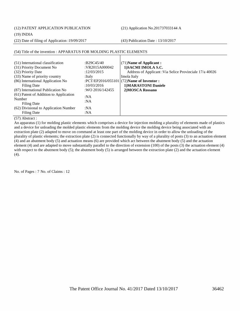
The Patent Office Journal No. 41/2017 Dated 13/10/2017 36462
(12) PATENT APPLICATION PUBLICATION (21) Application No.201737033144 A
(19) INDIA
(22) Date of filing of Application :19/09/2017 (43) Publication Date : 13/10/2017
(54) Title of the invention : APPARATUS FOR MOLDING PLASTIC ELEMENTS
(51) International classification :B29C45/40
(31) Priority Document No :VR2015A000042
(32) Priority Date :12/03/2015
(33) Name of priority country :Italy
(86) International Application No
Filing Date
:PCT/EP2016/055101
:10/03/2016
(87) International Publication No :WO 2016/142455
(61) Patent of Addition to Application
Number
Filing Date
:NA
:NA
(62) Divisional to Application Number
Filing Date
:NA
:NA
(71)Name of Applicant :
1)SACMI IMOLA S.C. Address of Applicant :Via Selice Provinciale 17/a 40026
Imola Italy
(72)Name of Inventor :
1)MARASTONI Daniele
2)MOSCA Rossano
(57) Abstract :
An apparatus (1) for molding plastic elements which comprises a device for injection molding a plurality of elements made of plastics
and a device for unloading the molded plastic elements from the molding device the molding device being associated with an
extraction plate (2) adapted to move on command at least one part of the molding device in order to allow the unloading of the
plurality of plastic elements; the extraction plate (2) is connected functionally by way of a plurality of posts (3) to an actuation element
(4) and an abutment body (5) and actuation means (6) are provided which act between the abutment body (5) and the actuation
element (4) and are adapted to move substantially parallel to the direction of extension (100) of the posts (3) the actuation element (4)
with respect to the abutment body (5); the abutment body (5) is arranged between the extraction plate (2) and the actuation element
(4).
No. of Pages : 7 No. of Claims : 12
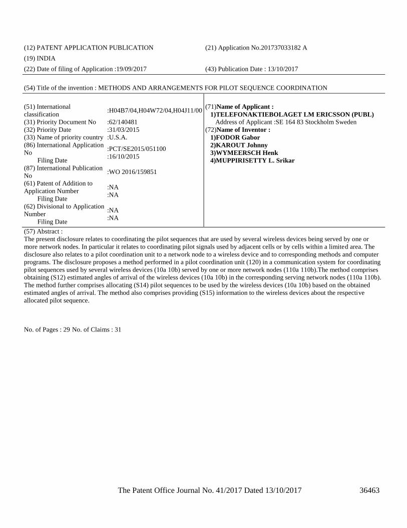
The Patent Office Journal No. 41/2017 Dated 13/10/2017 36463
(12) PATENT APPLICATION PUBLICATION (21) Application No.201737033182 A
(19) INDIA
(22) Date of filing of Application :19/09/2017 (43) Publication Date : 13/10/2017
(54) Title of the invention : METHODS AND ARRANGEMENTS FOR PILOT SEQUENCE COORDINATION
(51) International
classification :H04B7/04,H04W72/04,H04J11/00
(31) Priority Document No :62/140481
(32) Priority Date :31/03/2015
(33) Name of priority country :U.S.A.
(86) International Application
No
Filing Date
:PCT/SE2015/051100
:16/10/2015
(87) International Publication
No :WO 2016/159851
(61) Patent of Addition to
Application Number
Filing Date
:NA
:NA
(62) Divisional to Application
Number
Filing Date
:NA
:NA
(71)Name of Applicant :
1)TELEFONAKTIEBOLAGET LM ERICSSON (PUBL) Address of Applicant :SE 164 83 Stockholm Sweden
(72)Name of Inventor :
1)FODOR Gabor
2)KAROUT Johnny
3)WYMEERSCH Henk
4)MUPPIRISETTY L. Srikar
(57) Abstract :
The present disclosure relates to coordinating the pilot sequences that are used by several wireless devices being served by one or
more network nodes. In particular it relates to coordinating pilot signals used by adjacent cells or by cells within a limited area. The
disclosure also relates to a pilot coordination unit to a network node to a wireless device and to corresponding methods and computer
programs. The disclosure proposes a method performed in a pilot coordination unit (120) in a communication system for coordinating
pilot sequences used by several wireless devices (10a 10b) served by one or more network nodes (110a 110b).The method comprises
obtaining (S12) estimated angles of arrival of the wireless devices (10a 10b) in the corresponding serving network nodes (110a 110b).
The method further comprises allocating (S14) pilot sequences to be used by the wireless devices (10a 10b) based on the obtained
estimated angles of arrival. The method also comprises providing (S15) information to the wireless devices about the respective
allocated pilot sequence.
No. of Pages : 29 No. of Claims : 31
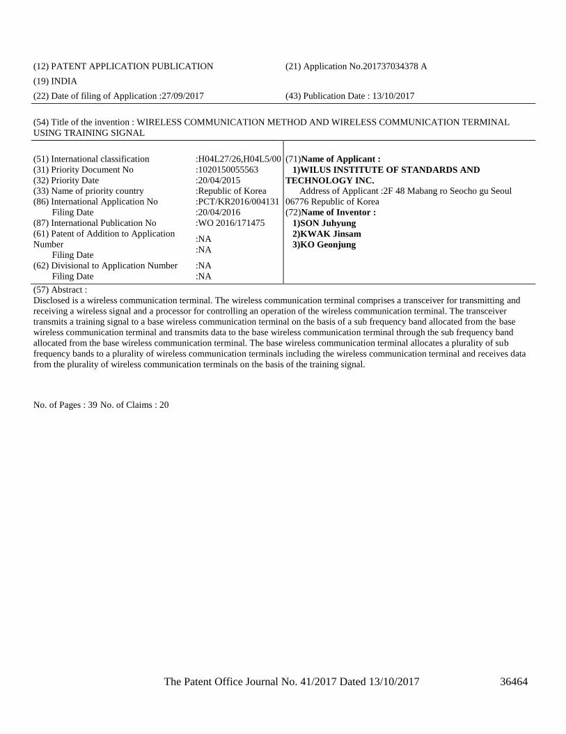
The Patent Office Journal No. 41/2017 Dated 13/10/2017 36464
(12) PATENT APPLICATION PUBLICATION (21) Application No.201737034378 A
(19) INDIA
(22) Date of filing of Application :27/09/2017 (43) Publication Date : 13/10/2017
(54) Title of the invention : WIRELESS COMMUNICATION METHOD AND WIRELESS COMMUNICATION TERMINAL
USING TRAINING SIGNAL
(51) International classification :H04L27/26,H04L5/00
(31) Priority Document No :1020150055563
(32) Priority Date :20/04/2015
(33) Name of priority country :Republic of Korea
(86) International Application No
Filing Date
:PCT/KR2016/004131
:20/04/2016
(87) International Publication No :WO 2016/171475
(61) Patent of Addition to Application
Number
Filing Date
:NA
:NA
(62) Divisional to Application Number
Filing Date
:NA
:NA
(71)Name of Applicant :
1)WILUS INSTITUTE OF STANDARDS AND
TECHNOLOGY INC. Address of Applicant :2F 48 Mabang ro Seocho gu Seoul
06776 Republic of Korea
(72)Name of Inventor :
1)SON Juhyung
2)KWAK Jinsam
3)KO Geonjung
(57) Abstract :
Disclosed is a wireless communication terminal. The wireless communication terminal comprises a transceiver for transmitting and
receiving a wireless signal and a processor for controlling an operation of the wireless communication terminal. The transceiver
transmits a training signal to a base wireless communication terminal on the basis of a sub frequency band allocated from the base
wireless communication terminal and transmits data to the base wireless communication terminal through the sub frequency band
allocated from the base wireless communication terminal. The base wireless communication terminal allocates a plurality of sub
frequency bands to a plurality of wireless communication terminals including the wireless communication terminal and receives data
from the plurality of wireless communication terminals on the basis of the training signal.
No. of Pages : 39 No. of Claims : 20
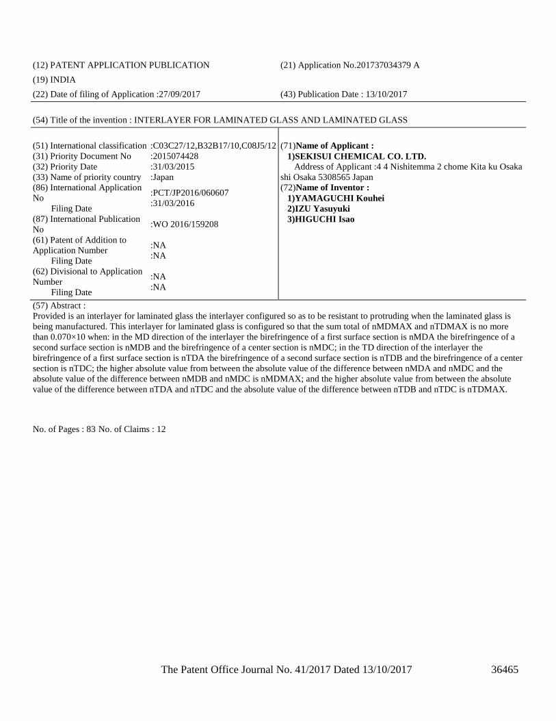
The Patent Office Journal No. 41/2017 Dated 13/10/2017 36465
(12) PATENT APPLICATION PUBLICATION (21) Application No.201737034379 A
(19) INDIA
(22) Date of filing of Application :27/09/2017 (43) Publication Date : 13/10/2017
(54) Title of the invention : INTERLAYER FOR LAMINATED GLASS AND LAMINATED GLASS
(51) International classification :C03C27/12,B32B17/10,C08J5/12
(31) Priority Document No :2015074428
(32) Priority Date :31/03/2015
(33) Name of priority country :Japan
(86) International Application
No
Filing Date
:PCT/JP2016/060607
:31/03/2016
(87) International Publication
No :WO 2016/159208
(61) Patent of Addition to
Application Number
Filing Date
:NA
:NA
(62) Divisional to Application
Number
Filing Date
:NA
:NA
(71)Name of Applicant :
1)SEKISUI CHEMICAL CO. LTD. Address of Applicant :4 4 Nishitemma 2 chome Kita ku Osaka
shi Osaka 5308565 Japan
(72)Name of Inventor :
1)YAMAGUCHI Kouhei
2)IZU Yasuyuki
3)HIGUCHI Isao
(57) Abstract :
Provided is an interlayer for laminated glass the interlayer configured so as to be resistant to protruding when the laminated glass is
being manufactured. This interlayer for laminated glass is configured so that the sum total of nMDMAX and nTDMAX is no more
than 0.070×10 when: in the MD direction of the interlayer the birefringence of a first surface section is nMDA the birefringence of a
second surface section is nMDB and the birefringence of a center section is nMDC; in the TD direction of the interlayer the
birefringence of a first surface section is nTDA the birefringence of a second surface section is nTDB and the birefringence of a center
section is nTDC; the higher absolute value from between the absolute value of the difference between nMDA and nMDC and the
absolute value of the difference between nMDB and nMDC is nMDMAX; and the higher absolute value from between the absolute
value of the difference between nTDA and nTDC and the absolute value of the difference between nTDB and nTDC is nTDMAX.
No. of Pages : 83 No. of Claims : 12
The Patent Office Journal No. 41/2017 Dated 13/10/2017 36466
(12) PATENT APPLICATION PUBLICATION (21) Application No.201737034667 A
(19) INDIA
(22) Date of filing of Application :29/09/2017 (43) Publication Date : 13/10/2017
(54) Title of the invention : APPARATUS AND METHOD FOR CONTROLLING POWER
(51) International classification :G02B27/01,H02J7/00,G06F3/01
(31) Priority Document No :1020150028756
(32) Priority Date :01/03/2015
(33) Name of priority country :Republic of Korea
(86) International Application
No
Filing Date
:PCT/KR2016/001991
:29/02/2016
(87) International Publication No :WO 2016/140475
(61) Patent of Addition to
Application Number
Filing Date
:NA
:NA
(62) Divisional to Application
Number
Filing Date
:NA
:NA
(71)Name of Applicant :
1)SAMSUNG ELECTRONICS CO. LTD. Address of Applicant :129 Samsung ro Yeongtong gu Suwon
si Gyeonggi do 16677 Republic of Korea
(72)Name of Inventor :
1)CHOI Youngjun
2)LEE Seungmin
3)KIM Heon Chol
4)CHO Ikhyun
(57) Abstract :
A power control method and an electronic device and/or connecting unit to implement the power control method is provided. The
electronic device includes a first interface unit configured to be connected to an external device that can receive and provide power to
the electronic device a second interface unit configured to be connected to an external charger that can provide power for the external
device and the electronic device and a main controller configured to detect whether or not the external charger is connected and
receive and direct power from the external device or the external charger according to whether or not the external charger is
connected.
No. of Pages : 18 No. of Claims : 15
The Patent Office Journal No. 41/2017 Dated 13/10/2017 36467
(12) PATENT APPLICATION PUBLICATION (21) Application No.201737034794 A
(19) INDIA
(22) Date of filing of Application :29/09/2017 (43) Publication Date : 13/10/2017
(54) Title of the invention : ANTENNA DEVICE AND ELECTRONIC APPARATUS
(51) International classification :H01Q7/00,H01Q1/38
(31) Priority Document No :2016004898
(32) Priority Date :14/01/2016
(33) Name of priority country :Japan
(86) International Application No
Filing Date
:PCT/JP2017/000961
:13/01/2017
(87) International Publication No :WO 2017/122764
(61) Patent of Addition to Application
Number
Filing Date
:NA
:NA
(62) Divisional to Application Number
Filing Date
:NA
:NA
(71)Name of Applicant :
1)MURATA MANUFACTURING CO. LTD. Address of Applicant :10 1 Higashikotari 1 chome
Nagaokakyo shi Kyoto 6178555 Japan
(72)Name of Inventor :
1)TENNO Nobuyuki
(57) Abstract :
This antenna device is provided with: a wiring substrate (110); a conductive member which is formed on a surface of the wiring
substrate (110) and has a first conductor part (11) and linear second conductor parts (21A 21B) which conduct electricity
therebetween; a coil element (20) having a coupling coil to which a power supply circuit is connected; and a capacitor (3). The first
conductor part (11) has a conductor opening (OP) and a gap (G1) that connects an outer edge of the first conductor part (11) and the
conductor opening (OP) and the capacitor (3) is disposed to cross over the gap (G1). The second conductor parts (21A 21B) are
connected to two points on an inner edge of the conductor opening (OP) and form a loop shaped current path together with a portion
of the first conductor part (11) and the capacitor (3). The coupling coil of the coil element (20) is magnetically coupled to the loop
shaped current path.
No. of Pages : 75 No. of Claims : 14
The Patent Office Journal No. 41/2017 Dated 13/10/2017 36468
(12) PATENT APPLICATION PUBLICATION (21) Application No.1227/KOL/2015 A
(19) INDIA
(22) Date of filing of Application :01/12/2015 (43) Publication Date : 13/10/2017
(54) Title of the invention : A SYSTEM AND A DEVICE FOR CONTINUOUS DELIVERY OF COMPLEX AND REGULATED
COLLOIDAL PARTICLES
(51) International classification :C08J3/28
(31) Priority Document No :NA
(32) Priority Date :NA
(33) Name of priority country :NA
(86) International Application No
Filing Date
:NA
:NA
(87) International Publication No : NA
(61) Patent of Addition to Application Number
Filing Date
:NA
:NA
(62) Divisional to Application Number
Filing Date
:NA
:NA
(71)Name of Applicant :
1)ITC LIMITED Address of Applicant :37, J.L. Nehru Road, Kolkata-700071,
State of West Bengal, India
(72)Name of Inventor :
1)SATHYASEELAN, Rejimon
2)BAKSHI, Soumyadeep
(57) Abstract :
A system and device for continuous delivery of complex and regulated colloidal particles is provided. It comprises of : an electronic
circuit and a switch to control the supply of power; an aerodynamic flow proposer means to create a flow of carrier gas through a
vertical axis; a hollow support means coupled to said aerodynamic flow proposer means, having a vertical tube and an opening to
allow carrier gas to flow through; a colloid generation means coupled to the support member means for generating colloidal particles;
a controller means to control vaporization of colloidal particles; an outlet for the vaporized colloidal particles to disperse into the
surrounding environment and optionally, a light generating element mounted on top; wherein the system or device has a controller
means to generate a time based pulse width modulated signal.
No. of Pages : 20 No. of Claims : 11
The Patent Office Journal No. 41/2017 Dated 13/10/2017 36469
(12) PATENT APPLICATION PUBLICATION (21) Application No.1228/KOL/2015 A
(19) INDIA
(22) Date of filing of Application :01/12/2015 (43) Publication Date : 13/10/2017
(54) Title of the invention : A SYSTEM AND METHOD FOR ACCELERATED MEASURING OF BURN CHARACTERISTICS
OF AN ARTICLE
(51) International classification :F23N3/00
(31) Priority Document No :NA
(32) Priority Date :NA
(33) Name of priority country :NA
(86) International Application No
Filing Date
:NA
:NA
(87) International Publication No : NA
(61) Patent of Addition to Application Number
Filing Date
:NA
:NA
(62) Divisional to Application Number
Filing Date
:NA
:NA
(71)Name of Applicant :
1)ITC LIMITED Address of Applicant :37, J.L. Nehru Road, Kolkata-700071,
State of West Bengal, India West Bengal India
(72)Name of Inventor :
1)DEY, Bablu, Kumar
2)SAXENA, Pranjal
3)SAMANTA, Prasad
4)PAL, Kiran
5)BHATT, Saumya
(57) Abstract :
The present invention discloses an accelerated measurement system for a defect in smoking article which cannot be directly measured
in the existing quality checks of any tobacco industry. All physical quality parameters which are normally measured in a tobacco plant
can only contribute to the possibility of a hot coal fall off (HCFO) defect but will not be able to measure tendency of this defect or
complaint comes from the market. The present invention builds an accelerated testing model which simulates the normal smoking and
tapping behaviour but with increased force.
No. of Pages : 27 No. of Claims : 16
The Patent Office Journal No. 41/2017 Dated 13/10/2017 36470
(12) PATENT APPLICATION PUBLICATION (21) Application No.201734010891 A
(19) INDIA
(22) Date of filing of Application :28/03/2017 (43) Publication Date : 13/10/2017
(54) Title of the invention : HOSE PUMP
(51) International classification :F04C5/00
(31) Priority Document No :202016101907.9
(32) Priority Date :11/04/2016
(33) Name of priority country :Germany
(86) International Application No
Filing Date
:NA
:NA
(87) International Publication No : NA
(61) Patent of Addition to Application Number
Filing Date
:NA
:NA
(62) Divisional to Application Number
Filing Date
:NA
:NA
(71)Name of Applicant :
1)ULRICH GMBH & CO. KG Address of Applicant :BUCHBRUNNENWEG 12, 89081
ULM, Germany
(72)Name of Inventor :
1)Norbert BÜCKLE
(57) Abstract :
In a hose pump to convey a fluid guided in a hose, with a hose bed (2) having a counter support (4), a carrier disk (1)
rotatable relative to counter support (2) [sic; (4)], a number of pinch rollers (3) arranged equidistant from each other in the peripheral
direction on carrier disk (1) and a number of guide rollers (5) arranged equidistant from each other in the peripheral direction on
carrier disk (1), a guide roller (5) is arranged between two consecutive pinch rollers (3) in the peripheral direction of carrier disk (1),
and the pinch rollers (3) press a hose inserted into hose bed (2) against the counter support (4), while pinching the hose when the
carrier disk (1) is rotating in the conveying direction (F) in order to transport the fluid in the hose in the conveying direction. In order
also to ensure reliable threading of a hose section of a pump hose, when the hose section is somewhat
too short and in order to prevent automatic unthreading of the inserted hose section during operation of the hose pump, the
angular distance ( ) between a guide roller (5a) and the pinch roller (3b) preceding said guide roller (5a) in conveying direction
(F) is greater than the angular distance (d) between this 15 guide roller (5a) and the pinch roller (3a) following said guide roller
(5a) in conveying direction (F).
No. of Pages : 17 No. of Claims : 17
The Patent Office Journal No. 41/2017 Dated 13/10/2017 36471
(12) PATENT APPLICATION PUBLICATION (21) Application No.206/KOL/2015 A
(19) INDIA
(22) Date of filing of Application :25/02/2015 (43) Publication Date : 13/10/2017
(54) Title of the invention : A RECIRCULATING WATER TREATMENT SIMULATOR.
(51) International classification :B01D65/00
(31) Priority Document No :NA
(32) Priority Date :NA
(33) Name of priority country :NA
(86) International Application No
Filing Date
:NA
:NA
(87) International Publication No : NA
(61) Patent of Addition to Application Number
Filing Date
:NA
:NA
(62) Divisional to Application Number
Filing Date
:NA
:NA
(71)Name of Applicant :
1)STEEL AUTHORITY OF INDIA LIMITED Address of Applicant :Research & Development Centre for
Iron & Steel, Doranda, Ranchi-834002, State of Jharkhand, India.
(72)Name of Inventor :
1)MITRA MAZUMDER SUBHAJIT
2)AGRAWAL ROOPAK
3)OJHA KAMAL DEO
4)TIWARI SATYENDRA NATH
5)CHOUBEY MUKTESHWAR
(57) Abstract :
The present invention relates to a recirculating water treatment simulator for simulating the process parameters and chemical dosing
for recirculating water treatment in any industry such as closed loop cooling water treatment in steel industry, including treating and
reusing wastewater in the cooling water circuit favouring optimum use of treatment chemicals and online evaluation of treatment
effectiveness to maintain water quality parameters at desired level. Importantly, the system/simulator according to the present
invention would act as a decision support tool to have control over chemical treatment of recirculating cooling water; i.e, control over
inhibitor addition for optimum corrosion protection, comparison between various inhibitors to compare their efficacy, possibility of
replacement of costly proprietary inhibitors with generic inhibitors, monitoring of corrosivity and deposition trends under
various treatment and process conditions, thus favouring wide scale application and use in various industry. (Figure 1)
No. of Pages : 33 No. of Claims : 17
The Patent Office Journal No. 41/2017 Dated 13/10/2017 36472
(12) PATENT APPLICATION PUBLICATION (21) Application No.201737031940 A
(19) INDIA
(22) Date of filing of Application :09/09/2017 (43) Publication Date : 13/10/2017
(54) Title of the invention : LBT PATTERNS FOR WIRELESS COMMUNICATION
(51) International classification :H04W74/04,H04W16/14
(31) Priority Document No :NA
(32) Priority Date :NA
(33) Name of priority country :NA
(86) International Application No
Filing Date
:PCT/SE2015/050199
:20/02/2015
(87) International Publication No :WO 2016/133441
(61) Patent of Addition to Application
Number
Filing Date
:NA
:NA
(62) Divisional to Application Number
Filing Date
:NA
:NA
(71)Name of Applicant :
1)TELEFONAKTIEBOLAGET LM ERICSSON (PUBL) Address of Applicant :S 164 83 Stockholm Sweden
(72)Name of Inventor :
1)KOUTSIMANIS Chrysostomos
2)GODANA Bruhtesfa
3)KAZMI Muhammad
(57) Abstract :
The present disclosure pertains to a method of operating a wireless device in a wireless communication network wherein the wireless
device is adapted to transmit data based on pre determined communication schedules each communication schedule pertaining to a
scheduling time interval of predetermined length. The method comprises determining by the wireless device a pattern of expected
transmission accesses on at least a first transmission frequency spectrum accessed with Listen Before Talk (LBT) the pattern covering
a plurality of scheduling time intervals. The disclosure also pertains to corresponding devices and further methods.
No. of Pages : 57 No. of Claims : 12
The Patent Office Journal No. 41/2017 Dated 13/10/2017 36473
(12) PATENT APPLICATION PUBLICATION (21) Application No.201737031943 A
(19) INDIA
(22) Date of filing of Application :09/09/2017 (43) Publication Date : 13/10/2017
(54) Title of the invention : METHOD APPARATUS AND SYSTEM FOR IDENTITY AUTHENTICATION
(51) International classification :H04L9/08
(31) Priority Document No :201510084941.2
(32) Priority Date :16/02/2015
(33) Name of priority country :China
(86) International Application No
Filing Date
:PCT/US2016/016740
:05/02/2016
(87) International Publication No :WO 2016/133724
(61) Patent of Addition to Application
Number
Filing Date
:NA
:NA
(62) Divisional to Application Number
Filing Date
:NA
:NA
(71)Name of Applicant :
1)ALIBABA GROUP HOLDING LIMITED Address of Applicant :Fourth Floor One Capital Place P.O.
Box 847 George Town Grand Cayman Cayman Island
(72)Name of Inventor :
1)FU Yingfang
2)LIU Shuanlin
(57) Abstract :
An identity authentication method for a quantum key distribution process includes selecting by a sender preparation bases of an
identity authentication bit string in accordance with a preset basis vector selection rule; sending by a sender quantum states of the
identity authentication bit string and quantum states of a randomly generated key bit string by using different wavelengths. The
identity authentication bit string is interleaved in the key bit string at a random position and with a random length. The method further
includes measuring by a receiver the received quantum states in the quantum state information in accordance with the different
wavelengths and measurement bases selected according to the preset basis vector selection rule to obtain identity authentication
information from the measurement of the identity authentication bit string; and determining by the receiver whether the identity
authentication information obtained through the measurement corresponds with the preset basis vector selection rule.
No. of Pages : 42 No. of Claims : 26
The Patent Office Journal No. 41/2017 Dated 13/10/2017 36474
(12) PATENT APPLICATION PUBLICATION (21) Application No.201737031944 A
(19) INDIA
(22) Date of filing of Application :09/09/2017 (43) Publication Date : 13/10/2017
(54) Title of the invention : ENHANCED REDIRECTION HANDLING FROM POLICY SERVER
(51) International classification :G06Q20/00
(31) Priority Document No :62/130871
(32) Priority Date :10/03/2015
(33) Name of priority country :U.S.A.
(86) International Application No
Filing Date
:PCT/US2016/021744
:10/03/2016
(87) International Publication No :WO 2016/145177
(61) Patent of Addition to Application
Number
Filing Date
:NA
:NA
(62) Divisional to Application Number
Filing Date
:NA
:NA
(71)Name of Applicant :
1)AFFIRMED NETWORKS INC. Address of Applicant :35 Nagog Park 1st Floor Acton MA
01720 U.S.A.
(72)Name of Inventor :
1)GUNDAMARAJU Krishna
2)KAPPLA Srinivas
3)VEMURI Surya
(57) Abstract :
Systems and methods are disclosed for directing a mobile device user with insufficient mobile credit to secondary pay sites. A PCRF
receives a request from a mobile device corresponding to a user. The PCRF detects credit associated with a user mobile network usage
account is below a threshold and assigns a tag to the request the tag including redirect site information and secondary site
information the redirect site information including at least one network identifier corresponding to a redirect site and the secondary
site information including at least one network identifier corresponding to a payment site accessible by the user when the credit
associated with the user mobile network usage account is below the threshold. The PCRF transmits the request and the corresponding
tag to a PCEF for routing the user to the at least one of the redirect site and the at least one payment site.
No. of Pages : 14 No. of Claims : 20
The Patent Office Journal No. 41/2017 Dated 13/10/2017 36475
(12) PATENT APPLICATION PUBLICATION (21) Application No.201737031972 A
(19) INDIA
(22) Date of filing of Application :11/09/2017 (43) Publication Date : 13/10/2017
(54) Title of the invention : METHOD AND DEVICE FOR PRODUCING A TRIPLE INSULATED GLAZING
(51) International classification :E06B3/663,E06B3/677
(31) Priority Document No :15164591.8
(32) Priority Date :22/04/2015
(33) Name of priority country :EPO
(86) International Application No
Filing Date
:PCT/EP2016/058940
:21/04/2016
(87) International Publication No :WO 2016/170079
(61) Patent of Addition to Application
Number
Filing Date
:NA
:NA
(62) Divisional to Application Number
Filing Date
:NA
:NA
(71)Name of Applicant :
1)SAINT GOBAIN GLASS FRANCE Address of Applicant :18 avenue dAlsace 92400 Courbevoie
France
(72)Name of Inventor :
1)KUSTER Hans Werner
2)SCHREIBER Walter
(57) Abstract :
The invention relates to a method for producing a triple insulated glazing wherein at least a) one pane (15) is inserted into the groove
(6) of a spacer (I) and the spacer (I) is shaped in a peripheral manner in order to form a spacer frame (I ) which frames the pane (15) b)
a first pane (13) is connected to the first pane contact surface (2.1) of the spacer frame (I ) and a second pane (14) is connected to the
second pane contact surface (2,2) by means of the upper edge (28 ) and the lateral edges (28) and the lower edges (28) of the first pane
(13) and of the second pane (14) are bent outward c) pane intermediate spaces (17) are filled with protective gas from below and d) the
pane assembly consisting of the panes (13 14 15) and the spacer frame (I ) is closed and pressed together.
No. of Pages : 15 No. of Claims : 14
The Patent Office Journal No. 41/2017 Dated 13/10/2017 36476
(12) PATENT APPLICATION PUBLICATION (21) Application No.201737031980 A
(19) INDIA
(22) Date of filing of Application :11/09/2017 (43) Publication Date : 13/10/2017
(54) Title of the invention : APPARATUS AND METHOD FOR PROCESSING STEREO SIGNALS FOR REPRODUCTION IN
CARS TO ACHIEVE INDIVIDUAL THREE DIMENSIONAL SOUND BY FRONTAL LOUDSPEAKERS
(51) International classification :H04S5/00,H04S5/02
(31) Priority Document No :15161402.1
(32) Priority Date :27/03/2015
(33) Name of priority country :EPO
(86) International Application No
Filing Date
:PCT/EP2016/056618
:24/03/2016
(87) International Publication No :WO 2016/156237
(61) Patent of Addition to Application
Number
Filing Date
:NA
:NA
(62) Divisional to Application Number
Filing Date
:NA
:NA
(71)Name of Applicant :
1)FRAUNHOFER GESELLSCHAFT ZUR FÖRDERUNG
DER ANGEWANDTEN FORSCHUNG E.V. Address of Applicant : Hansastraße 27c 80686 München
Germany
(72)Name of Inventor :
1)HESS Wolfgang
2)HELLMUTH Oliver
3)VARGA Stefan
4)HABETS Emanuel
5)PLOGSTIES Jan 6)HERRE Jürgen
(57) Abstract :
Apparatus and method for processing stereo signals for reproduction in cars to achieve individual three dimensional sound by frontal
loudspeakers Embodiments provide a digital processor (100) comprising an ambient portion extractor (102) and a spatial effect
processing stage (104). The ambient portion extractor (102) is configured to extract an ambient portion from a multi channel signal.
The spatial effect processing stage (104) is configured to generate a spatial effect signal based on the ambient portion of the multi
channel signal. The digital processor (100) is configured to combine (116) the multi channel signal or a processed version thereof with
the spatial effect signal.
No. of Pages : 22 No. of Claims : 17
The Patent Office Journal No. 41/2017 Dated 13/10/2017 36477
(12) PATENT APPLICATION PUBLICATION (21) Application No.201737031985 A
(19) INDIA
(22) Date of filing of Application :11/09/2017 (43) Publication Date : 13/10/2017
(54) Title of the invention : EXPANDABLE SLOT CLOSURE FOR AN ELECTRIC MACHINE
(51) International classification :H02K3/493,H02K15/00
(31) Priority Document No :15161108.4
(32) Priority Date :26/03/2015
(33) Name of priority country :EPO
(86) International Application No
Filing Date
:PCT/EP2016/052670
:09/02/2016
(87) International Publication No :WO 2016/150610
(61) Patent of Addition to Application
Number
Filing Date
:NA
:NA
(62) Divisional to Application Number
Filing Date
:NA
:NA
(71)Name of Applicant :
1)SIEMENS AKTIENGESELLSCHAFT Address of Applicant :Werner von Siemens Straße 1 80333
München Germany
(72)Name of Inventor :
1) GRÜBEL André
2)SCHIRM Dieter
(57) Abstract :
The invention relates to a slot closing device (7) for closing a slot (2) in a stator (S) or rotor (R) of an electric machine (E) said device
(7) comprising a closure element (4) that contains a ferromagnetic material and includes a predetermined bending section (9) which
extends along a longitudinal direction of the closure element (4) and via which two leg portions (10) that form an obtuse angle (11) of
less than 180° therebetween are joined to one another. The aim of the invention is to be able to close the slot (2) in a low number of
steps. For this purpose an adhesive layer (5) is disposed on the edges (14) of the leg portions (10) and the adhesive layer (5) is
designed to harden under the effect of heat.
No. of Pages : 17 No. of Claims : 15
The Patent Office Journal No. 41/2017 Dated 13/10/2017 36478
(12) PATENT APPLICATION PUBLICATION (21) Application No.201737031998 A
(19) INDIA
(22) Date of filing of Application :11/09/2017 (43) Publication Date : 13/10/2017
(54) Title of the invention : PRACTICAL METHOD FOR MANUFACTURING 3 3 DIFLUORO 2 HYDROXYPROPIONIC ACID
(51) International
classification :C07C51/00,C07C59/115,C07C69/716
(31) Priority Document No :2015066966
(32) Priority Date :27/03/2015
(33) Name of priority
country :Japan
(86) International
Application No
Filing Date
:PCT/JP2016/058056
:15/03/2016
(87) International
Publication No :WO 2016/158365
(61) Patent of Addition to
Application Number
Filing Date
:NA
:NA
(62) Divisional to
Application Number
Filing Date
:NA
:NA
(71)Name of Applicant :
1)CENTRAL GLASS COMPANY LIMITED Address of Applicant :5253 Oaza Okiube Ube shi Yamaguchi
7550001 Japan
(72)Name of Inventor :
1)YAMAZAKI Takako
2)OKAMOTO Ryuichi
3)ISHII Akihiro
(57) Abstract :
2Provided is a practical method for manufacturing 3 3 difluoro 2 hydroxypropionic acid which is important as an intermediate for
medical and agricultural chemicals. By reacting a 4 4 difluoro 3 oxobutanoic acid ester with chlorine (Cl) a 4 4 difluoro 2 2 dichloro 3
oxobutanoic acid ester is obtained. By then reacting with an acid 3 3 difluoro 1 1 dichloro 2 propanone is obtained. Finally by reacting
with a basic aqueous solution 3 3 difluoro 2 hydroxypropionic acid can be manufactured.
No. of Pages : 24 No. of Claims : 5
The Patent Office Journal No. 41/2017 Dated 13/10/2017 36479
(12) PATENT APPLICATION PUBLICATION (21) Application No.201737032001 A
(19) INDIA
(22) Date of filing of Application :11/09/2017 (43) Publication Date : 13/10/2017
(54) Title of the invention : SINGLE ACTING HYDRAULIC CYLINDER
(51) International classification :F15B15/14
(31) Priority Document No :2015058144
(32) Priority Date :20/03/2015
(33) Name of priority country :Japan
(86) International Application No
Filing Date
:PCT/JP2016/057006
:07/03/2016
(87) International Publication No :WO 2016/152482
(61) Patent of Addition to Application
Number
Filing Date
:NA
:NA
(62) Divisional to Application Number
Filing Date
:NA
:NA
(71)Name of Applicant :
1)KYB CORPORATION Address of Applicant :World Trade Center Bldg. 4 1
Hamamatsu cho 2 chome Minato ku Tokyo 1056111 Japan
(72)Name of Inventor :
1)KUBOTA Takuya
2)SUEYOSHI Daisuke
(57) Abstract :
A single acting hydraulic cylinder 100 is provided with: a cylinder head 40 which is provided at the opening 10A of a cylinder tube 10
and through which a piston rod 20 is passed; a bush 60 which is provided at the inner periphery of the cylinder head 40 and which
supports the piston rod 20 in a slidable manner; and a housing recess 50 which is formed in the inner periphery of the cylinder head 40
and into which the bush 60 is press fitted from an inlet 50A. A bottom gap 51 filled with grease 70 is formed between the bush 60 and
the bottom surface 53 of the housing recess 50.
No. of Pages : 17 No. of Claims : 9
The Patent Office Journal No. 41/2017 Dated 13/10/2017 36480
(12) PATENT APPLICATION PUBLICATION (21) Application No.201737032023 A
(19) INDIA
(22) Date of filing of Application :11/09/2017 (43) Publication Date : 13/10/2017
(54) Title of the invention : ROTOR OF AN ASYNCHRONOUS MACHINE
(51) International classification :H02K1/32,H02K15/00
(31) Priority Document No :15163462.3
(32) Priority Date :14/04/2015
(33) Name of priority country :EPO
(86) International Application No
Filing Date
:PCT/EP2016/056999
:31/03/2016
(87) International Publication No :WO 2016/165947
(61) Patent of Addition to Application
Number
Filing Date
:NA
:NA
(62) Divisional to Application Number
Filing Date
:NA
:NA
(71)Name of Applicant :
1)SIEMENS AKTIENGESELLSCHAFT Address of Applicant :Werner von Siemens Straße 1 80333
München Germany
(72)Name of Inventor :
1)SCHERER Matthias
2)NIEDERMEYER Josef
3)SCHARF Uwe
(57) Abstract :
The invention relates to a rotor (7) of an asynchronous machine with at least one cage rotor wherein the rotor (7) has a least one
laminated core (8) with substantially axially extending conductors which are arranged in slots (14) in the rotor (7) and wherein the
conductors comprise at least two materials of different electrical conductivities wherein the material with the higher electrical
conductivity surrounds the material with the lower electrical conductivity by at least 65% when considered in the circumferential
direction.
No. of Pages : 16 No. of Claims : 9
The Patent Office Journal No. 41/2017 Dated 13/10/2017 36481
(12) PATENT APPLICATION PUBLICATION (21) Application No.201737032045 A
(19) INDIA
(22) Date of filing of Application :11/09/2017 (43) Publication Date : 13/10/2017
(54) Title of the invention : MANUFACTURING METHOD OF MOLDING MATERIAL
(51) International classification :B21D22/28,B21D22/20
(31) Priority Document No :2015070609
(32) Priority Date :31/03/2015
(33) Name of priority country :Japan
(86) International Application No
Filing Date
:PCT/JP2016/058136
:15/03/2016
(87) International Publication No :WO 2016/158383
(61) Patent of Addition to Application
Number
Filing Date
:NA
:NA
(62) Divisional to Application Number
Filing Date
:NA
:NA
(71)Name of Applicant :
1)NISSHIN STEEL CO. LTD. Address of Applicant :4 1 Marunouchi 3 chome Chiyoda ku
Tokyo 1008366 Japan
(72)Name of Inventor :
1)NAKAMURA Naofumi
2)YAMAMOTO Yudai
(57) Abstract :
By performing multi stage drawing with respect to a material metal plate a molding material (1) having a cylindrical trunk portion (10)
and a flange portion (11) formed at an end portion of the trunk portion is manufactured. In the multi stage drawing a preliminary
drawing that forms a preliminary body (20) having a trunk element (20a) from the material metal plate (2) a compression drawing that
is performed at least once after the preliminary drawing and that forms the trunk portion (10) by drawing the trunk element (20a)
while applying compressive force the pressure of which can be adjusted to the trunk element (20a) and a finishing ironing that is
performed at least once following the compression drawing and that is for securing dimensional accuracy.
No. of Pages : 29 No. of Claims : 4
The Patent Office Journal No. 41/2017 Dated 13/10/2017 36482
(12) PATENT APPLICATION PUBLICATION (21) Application No.201737032046 A
(19) INDIA
(22) Date of filing of Application :11/09/2017 (43) Publication Date : 13/10/2017
(54) Title of the invention : METHOD AND SYSTEM FOR TRANSPORTATION RESOURCE GROUPING AND
REALLOCATION
(51) International classification :G06Q50/30,G07B15/00
(31) Priority Document No :62/114956
(32) Priority Date :11/02/2015
(33) Name of priority country :U.S.A.
(86) International Application No
Filing Date
:PCT/US2016/017468
:11/02/2016
(87) International Publication No :WO 2016/130755
(61) Patent of Addition to Application
Number
Filing Date
:NA
:NA
(62) Divisional to Application Number
Filing Date
:NA
:NA
(71)Name of Applicant :
1)ARPENT LLC Address of Applicant :Suite 300 1755 Telstar Drive Colorado
Springs Colorado 80920 U.S.A.
(72)Name of Inventor :
1)SMITH Clint
2)SMITH Samuel
3)GANLEY Declan
(57) Abstract :
Systems and methods for dynamic transportation resource arbitrage (DTRA) may include configuring a server to dynamically manage
the use of transportation resources. The server may identify analyze organize and/or package available transportation resources
(e.g. segments of roadways in a geographical area etc.) as granular vehicular occupancy opportunity (VOO) elements/units that each
identify an amount of a resource that is offered for allocation and use to travelers. The granular VOO elements/units may be well
defined discrete standardized combinable and/or fungible information structures or units that are suitable for comparison and/or
mutual substitution. The server computing device may combine the granular VOOs to cover a specific corridor (e.g. an area that
encompasses ten miles of the left lane of a highway etc.) and dynamically offer a vehicle the right to access and use the transportation
resources identified by a combination of VOOs.
No. of Pages : 51 No. of Claims : 30
The Patent Office Journal No. 41/2017 Dated 13/10/2017 36483
(12) PATENT APPLICATION PUBLICATION (21) Application No.201737032077 A
(19) INDIA
(22) Date of filing of Application :11/09/2017 (43) Publication Date : 13/10/2017
(54) Title of the invention : DOOR PILLAR FOR CAR AND METHOD FOR MANUFACTURING DOOR PILLAR
(51) International classification :B60J5/04,B29C45/72,B29C45/73
(31) Priority Document No :1020150032195
(32) Priority Date :09/03/2015
(33) Name of priority country :Republic of Korea
(86) International Application
No
Filing Date
:PCT/KR2015/013728
:15/12/2015
(87) International Publication
No :WO 2016/143990
(61) Patent of Addition to
Application Number
Filing Date
:NA
:NA
(62) Divisional to Application
Number
Filing Date
:NA
:NA
(71)Name of Applicant :
1)KIM Ki Il Address of Applicant :205 1307 (Namyang dong Sungwon
APT.) 99 Daejeong ro Seongsan gu Changwon si Gyeongsangnam
do 51479 Republic of Korea
(72)Name of Inventor :
1)KIM Ki Il
(57) Abstract :
The present invention relates to a door pillar for a car and more specifically to a door pillar for a car that is manufactured using a
synthetic resin so as to be able to reduce the weight as well as improve workability. A door pillar for a car according to the present
invention comprises a body member and a wing member. The wing member provides: a bracket part on which a through hole for
being fixed to the car body using a screw is formed and a protrusion that can be inserted into the car body so as to fix the position of
the through hole; and a guide rail that is coupled to one side of the body member such that a car window can slide is formed. The body
member and the wing member are injected using a synthetic resin and integrally formed. Moreover with respect to the door pillar for a
car the wing member preferably has a plurality of injection holes formed along the length direction so as to prevent distortions in the
size when injecting the synthetic resin. According to the present invention the body member and the wing member are integrally
formed of synthetic resin and thus the manufacturing process for the door pillar for a car is simplified and furthermore the weight of
the door pillar can be reduced. More specifically the objective of the described method for manufacturing a door pillar for a car
according to the present invention is a method for manufacturing a door pillar for a car by manufacturing by injection using
poly(methylmethacrylate) so as not to require a coating process. The method for manufacturing a door pillar for a car according to one
aspect of the present invention comprises a drying step an insertion step a heating step a measurement step an injection step and a
cooling step. The drying step dries poly(methylmethacrylate). The insertion step inserts the poly(methylmethacrylate) dried in the
drying step into an injection cylinder. The heating step heats the cylinder into which the poly(methylmethacrylate) is inserted at
various different temperatures along the length direction. The measurement step measures the amount of poly(methylmethacrylate) to
inject. The injection step injects the measured poly(methylmethacrylate) into a mould at a constant pressure. The cooling step cools at
various different temperatures along the length direction relative to the injection holes of the mould into which the
poly(methylmethacrylate) is injected. According to the present invention a door pillar is manufactured by injecting
poly(methylmethacrylate) into a mould wherein the mould is divided into several levels and then the respective levels are cooled
differently and as a result a coating process is not required. Therefore not only can a manufacturing process for a door pillar be
simplified but also a door pillar can be manufactured in an environmentally friendly manner since the manufacturing process does not
emit any environmental pollutants.
No. of Pages : 17 No. of Claims : 17
The Patent Office Journal No. 41/2017 Dated 13/10/2017 36484
(12) PATENT APPLICATION PUBLICATION (21) Application No.201737031605 A
(19) INDIA
(22) Date of filing of Application :06/09/2017 (43) Publication Date : 13/10/2017
(54) Title of the invention : COMPOUNDS COMPOSITIONS AND METHODS FOR THE TREATMENT OF INFLAMMATORY
DEGENERATIVE AND NEURODEGENERATIVE DISEASES
(51) International classification :C07C51/09
(31) Priority Document No :62/113893
(32) Priority Date :09/02/2015
(33) Name of priority country :U.S.A.
(86) International Application No
Filing Date
:PCT/US2016/017112
:09/02/2016
(87) International Publication No :WO 2016/130522
(61) Patent of Addition to Application
Number
Filing Date
:NA
:NA
(62) Divisional to Application Number
Filing Date
:NA
:NA
(71)Name of Applicant :
1)BOARD OF SUPERVISORS OF LOUISIANA STATE
UNIVERSITY AND AGRICULTURAL AND
MECHANICAL COLLEGE Address of Applicant :3810 W. Lakeshore Drive Baton Rouge
LA 70808 U.S.A.
2)UNIVERSITY OF SOUTHERN CALIFORNIA (72)Name of Inventor :
1)BAZAN Nicolas G.
2)PETASIS Nicos A.
(57) Abstract :
This disclosure provides compounds pharmaceutical compositions and methods of use for the prevention and treatment of
inflammatory diseases or degenerative diseases including neurodegenerative diseases. Embodiments of the present disclosure provide
compounds related to very long chain polyunsaturated fatty acids pharmaceutical compositions containing the provided
compounds and methods of treating a subject with a condition or disease using provided compounds or pharmaceutical compositions.
No. of Pages : 46 No. of Claims : 48
The Patent Office Journal No. 41/2017 Dated 13/10/2017 36485
(12) PATENT APPLICATION PUBLICATION (21) Application No.201737031606 A
(19) INDIA
(22) Date of filing of Application :06/09/2017 (43) Publication Date : 13/10/2017
(54) Title of the invention : IMPROVED GAS BURNER WITH MULTI RINGS MAIN FLAMES.
(51) International classification :F23D14/04,F23D14/06
(31) Priority Document No :VE2015A000017
(32) Priority Date :24/04/2015
(33) Name of priority country :Italy
(86) International Application No
Filing Date
:PCT/IB2016/052272
:21/04/2016
(87) International Publication No :WO 2016/170497
(61) Patent of Addition to Application
Number
Filing Date
:NA
:NA
(62) Divisional to Application Number
Filing Date
:NA
:NA
(71)Name of Applicant :
1)DEFENDI ITALY S.R.L. Address of Applicant :Via Direttissima del Conero 29 60021
Camerano Italy
(72)Name of Inventor :
1)BRECCIA Luca
2)EMILIANI Girolamo
3)SBAFFI Marco
(57) Abstract :
An improved gas burner with multiple rings of main flames characterised by comprising: an injector holder structure (2) provided
with means (16) for its installation on the upper sheet metal of a cooking hob a central distribution chamber provided with in a central
flam e divider element (44 86) which is rigid with said injector holder structure (2) and is configured to generate a central ring of
flames said central distribution chamber (44) being closed upperly by a circular cover (6) an annular distribution chamber provided
within an annular flame divider element (4) which is rested on said injector holder structure (2) and is configured to generate at least
one ring of main flames which is concentric with said central ring of flames said annular distribution chamber (4) being separated
from said central distribution chamber (44) by an annular space (57) and being closed upperly by an annular cover (8) a first venturi
conduit (32 32 ) and a second venturi conduit (36 36 ) which are substantially horizontal and parallel and situated in said injector
holder structure (2) within the plan outline defined by said annular flame divider element (4) and have an inlet end facing a respective
injector (22 30) associated with a lateral wal l of respective adjacent cavities ( 1 8 24) provided in said injector holder structure (2) and
an outer end opening into respective cavities (34 38) in fluidic connection respectively with said central distribution chamber and with
said annular distribution chamber (4).
No. of Pages : 18 No. of Claims : 16
The Patent Office Journal No. 41/2017 Dated 13/10/2017 36486
(12) PATENT APPLICATION PUBLICATION (21) Application No.201737031608 A
(19) INDIA
(22) Date of filing of Application :06/09/2017 (43) Publication Date : 13/10/2017
(54) Title of the invention : INTEGRATING CIRCUIT AND CAPACITANCE SENSING CIRCUIT
(51) International classification :G06F3/044
(31) Priority Document No :201511031728.1
(32) Priority Date :31/12/2015
(33) Name of priority country :China
(86) International Application No
Filing Date
:PCT/CN2016/113974
:30/12/2016
(87) International Publication No :WO 2017/114514
(61) Patent of Addition to Application
Number
Filing Date
:NA
:NA
(62) Divisional to Application Number
Filing Date
:NA
:NA
(71)Name of Applicant :
1)SHENZHEN GOODIX TECHNOLOGY CO.LTD. Address of Applicant :Floor 13 Phase BTengfei Industrial
BuildingFutian Free Trade Zone Shenzhen Guangdong 518045
China
(72)Name of Inventor :
1)WEN Ya Nan
2)YANG Fu Chiang
3)LIANG Yingsi
(57) Abstract :
An integrating circuit applicable for the technical field of touch control comprising: an impedance unit (142) an amplifier (Amp) an
integrating capacitor (C) a discharging circuit (C) a first switch (SW1) and a second switch (SW2). The amplifier (Amp) includes a
first input end a second input end and an output end for outputting a first output signal; the integrating capacitor (C) is coupled
between the first input end and the output end; the discharging capacitor (C) includes a first end and a second end wherein the first end
is used for receiving a first voltage (Vs); the first switch (SW1) is coupled between the first input end of the amplifier (Amp) and the
second end of the discharging capacitor (C); and the second switch (SW2) is coupled between the first end and the second end of the
discharging capacitor (C). The integrating circuit can effectively sensing the variation in a capacitance.
No. of Pages : 18 No. of Claims : 23
The Patent Office Journal No. 41/2017 Dated 13/10/2017 36487
(12) PATENT APPLICATION PUBLICATION (21) Application No.201737031611 A
(19) INDIA
(22) Date of filing of Application :06/09/2017 (43) Publication Date : 13/10/2017
(54) Title of the invention : SECURITY ELEMENT AND SECURITY DOCUMENT
(51) International
classification :B42D25/324,B42D25/351,B42D25/355
(31) Priority Document
No :1552120
(32) Priority Date :16/03/2015
(33) Name of priority
country :France
(86) International
Application No
Filing Date
:PCT/EP2016/055371
:11/03/2016
(87) International
Publication No :WO 2016/146551
(61) Patent of Addition to
Application Number
Filing Date
:NA
:NA
(62) Divisional to
Application Number
Filing Date
:NA
:NA
(71)Name of Applicant :
1)OBERTHUR FIDUCIAIRE Address of Applicant :7 avenue de Messine 75008 PARIS
France
(72)Name of Inventor :
1)MALLOL Stéphane
2)THIERRY Yvan
(57) Abstract :
The invention relates to a security element (20) for a security document (10) comprising: a first perforated layer (24) made from a first
material defining at least one half tone raster pattern and a second layer (26) which is semi transparent and made from a second
material different from the first said second layer being visible at least through a hole in the first layer.
No. of Pages : 18 No. of Claims : 23
The Patent Office Journal No. 41/2017 Dated 13/10/2017 36488
(12) PATENT APPLICATION PUBLICATION (21) Application No.201737031633 A
(19) INDIA
(22) Date of filing of Application :07/09/2017 (43) Publication Date : 13/10/2017
(54) Title of the invention : APPARATUS AND METHOD FOR MANAGING RADIO LINK IN WIRELESS COMMUNICATION
SYSTEM
(51) International classification :H04B7/06
(31) Priority Document No :1020150046352
(32) Priority Date :01/04/2015
(33) Name of priority country :Republic of Korea
(86) International Application No
Filing Date
:PCT/KR2016/003391
:01/04/2016
(87) International Publication No :WO 2016/159708
(61) Patent of Addition to Application
Number
Filing Date
:NA
:NA
(62) Divisional to Application Number
Filing Date
:NA
:NA
(71)Name of Applicant :
1)SAMSUNG ELECTRONICS CO. LTD. Address of Applicant :129 Samsung ro Yeongtong gu Suwon
si Gyeonggi do 16677 Republic of Korea
(72)Name of Inventor :
1)JUNG Doyoung
2)KWON Changyeul
3)ROH Donghwi
4)YOON Sungrok
5)LEE Seok Yong
6)JO Ohyun
(57) Abstract :
A method of operating a transmission device in a wireless communication system includes: determining a reception state of a
reception device; and performing beamforming based on the reception state.
No. of Pages : 38 No. of Claims : 15
The Patent Office Journal No. 41/2017 Dated 13/10/2017 36489
(12) PATENT APPLICATION PUBLICATION (21) Application No.201737031638 A
(19) INDIA
(22) Date of filing of Application :07/09/2017 (43) Publication Date : 13/10/2017
(54) Title of the invention : METHOD OF WELDING METAL BASED NON WELDABLE DIRECTLY TO EACH OTHER
MATERIALS USING A SPACER
(51) International
classification :B23K9/173,B23K10/02,B23K11/06
(31) Priority Document No :15158962.9
(32) Priority Date :13/03/2015
(33) Name of priority country :EPO
(86) International
Application No
Filing Date
:PCT/EP2016/055259
:11/03/2016
(87) International Publication
No :WO 2016/146511
(61) Patent of Addition to
Application Number
Filing Date
:NA
:NA
(62) Divisional to
Application Number
Filing Date
:NA
:NA
(71)Name of Applicant :
1)OUTOKUMPU OYJ Address of Applicant :Salmisaarenranta 11 00180 Helsinki
Finland
(72)Name of Inventor :
1)LINDNER Stefan
2)SKRLEC Jasminko
(57) Abstract :
The invention relates to a method of welding of at least two metal based materials (5 7) non weldable directly to each other with
resistance welding. At least one spacer (6) is joined by welding on at least one of the two surfaces of a material (5) in every interstice
between two surfaces of materials to be welded. The welded spacer (6) is utilized so that resistance welding is focused to the surface
of the material (5) with the spacer (6) to melt at least one spacer (6) located on the heat affecting zone in order to achieve a weld
between the metal based materials (5 7).
No. of Pages : 11 No. of Claims : 22
The Patent Office Journal No. 41/2017 Dated 13/10/2017 36490
(12) PATENT APPLICATION PUBLICATION (21) Application No.201737031647 A
(19) INDIA
(22) Date of filing of Application :07/09/2017 (43) Publication Date : 13/10/2017
(54) Title of the invention : VERTICAL ROLL MILL
(51) International classification :B02C15/00,B02C23/10
(31) Priority Document No :10 2015 203 856.4
(32) Priority Date :04/03/2015
(33) Name of priority country :Germany
(86) International Application No
Filing Date
:PCT/EP2016/053905
:25/02/2016
(87) International Publication No :WO 2016/139105
(61) Patent of Addition to Application
Number
Filing Date
:NA
:NA
(62) Divisional to Application Number
Filing Date
:NA
:NA
(71)Name of Applicant :
1)THYSSENKRUPP INDUSTRIAL SOLUTIONS AG Address of Applicant :ThyssenKrupp Allee 1 45143 Essen
Germany
2)thyssenkrupp AG (72)Name of Inventor :
1)ASSMANN Björn Olaf
2)SACHSE Carsten
(57) Abstract :
The invention relates to a vertical roll mill (10) comprising a bypass device (70) for discharging particles that are difficult to grind e.g.
ductile particles such as iron particles from the grinding process.
No. of Pages : 11 No. of Claims : 17
The Patent Office Journal No. 41/2017 Dated 13/10/2017 36491
(12) PATENT APPLICATION PUBLICATION (21) Application No.201737031697 A
(19) INDIA
(22) Date of filing of Application :07/09/2017 (43) Publication Date : 13/10/2017
(54) Title of the invention : METHOD FOR TRIGGERING AN AUTOMATIC EMERGENCY BRAKING PROCESS WITH
VARIABLE WARNING TIME PERIOD
(51) International classification :B60T8/32
(31) Priority Document No :10 2015 104 547.8
(32) Priority Date :26/03/2015
(33) Name of priority country :Germany
(86) International Application No
Filing Date
:PCT/EP2016/055724
:16/03/2016
(87) International Publication No :WO 2016/162178
(61) Patent of Addition to Application
Number
Filing Date
:NA
:NA
(62) Divisional to Application Number
Filing Date
:NA
:NA
(71)Name of Applicant :
1)KNORR BREMSE SYSTEME FÜR NUTZFAHRZEUGE
GMBH Address of Applicant :Moosacher Str. 80 80809 München
Germany
(72)Name of Inventor :
1)HECKER Falk 2) GÜCKER Ulrich
3)KRABOT Matyas
4)KLEIN Markus
5)DOCZY Csaba
6)JOZSA Gergely
7)ROZSA Tamas
(57) Abstract :
The invention relates to a method for triggering an automatic emergency braking process in a vehicle for avoiding a tail end collision
with an obstacle wherein a warning to the driver is triggered if at least one warning condition is satisfied wherein the satisfaction of
the warning condition specifies that owing to the instantaneous driving situation of the vehicle relative to the obstacle the automatic
emergency braking process should be triggered wherein the automatic emergency braking process is not triggered until after the
warning to the driver is triggered and a warning time period (tWarning) has subsequently expired. The invention provides that the
warning time period (tWarning) is set as a function of the relative movement situation between the vehicle and the obstacle and/or is
adapted as a function of a relative movement situation between the vehicle and the obstacle which changes over time.
No. of Pages : 19 No. of Claims : 11
The Patent Office Journal No. 41/2017 Dated 13/10/2017 36492
(12) PATENT APPLICATION PUBLICATION (21) Application No.201737031715 A
(19) INDIA
(22) Date of filing of Application :07/09/2017 (43) Publication Date : 13/10/2017
(54) Title of the invention : ELECTRONIC APPARATUS
(51) International classification :H05K1/14,H04M1/02
(31) Priority Document No :NA
(32) Priority Date :NA
(33) Name of priority country :NA
(86) International Application No
Filing Date
:PCT/CN2015/091652
:10/10/2015
(87) International Publication No :WO 2017/059594
(61) Patent of Addition to Application
Number
Filing Date
:NA
:NA
(62) Divisional to Application Number
Filing Date
:NA
:NA
(71)Name of Applicant :
1)HUAWEI TECHNOLOGIES CO. LTD. Address of Applicant :Huawei Administration Building
BantianLonggang District Shenzhen Guangdong 518129 China
(72)Name of Inventor :
1)QIAN Chenyang
(57) Abstract :
An electronic apparatus which comprises a body (10) a display screen module (20) a battery (30) and a shell (40) wherein the body
(10) comprises an accommodating groove (11) a battery groove (13) and a circuit board (15); the body (10) comprises a first surface
(101) and a second surface (102) opposite to the first surface (101); the accommodating groove (11) is located on the first surface
(101); the battery groove (13) is located on the second surface (102) and the circuit board (15) is adjacent to the battery groove (13); a
flexible circuit board (21) is arranged on the display screen module (20); an opening (112) is arranged at a groove bottom wall of the
accommodating groove (11) and the opening (112) runs through one end at which the battery groove (13) is arranged of the second
surface (102); the battery (30) is accommodated in the battery groove (13); the shell (40) covers the body (10) to seal the battery
groove (13); the display screen module (20) is accommodated in the accommodating groove (11); and the flexible circuit board (21)
penetrates through the opening (112) bypasses one side of the battery groove (13) and reaches the surface facing towards the shell
(40) of the battery (30) and extends along the surface until the flexible circuit board is connected to the circuit board (15).
No. of Pages : 13 No. of Claims : 15
The Patent Office Journal No. 41/2017 Dated 13/10/2017 36493
(12) PATENT APPLICATION PUBLICATION (21) Application No.201737031716 A
(19) INDIA
(22) Date of filing of Application :07/09/2017 (43) Publication Date : 13/10/2017
(54) Title of the invention : NOX TRAP CATALYST SUPPORT MATERIAL WITH IMPROVED STABILITY AGAINST
BAAI2O4 FORMATION
(51) International classification :C01F7/16,B01D53/94,B01J37/02
(31) Priority Document No :15158315.0
(32) Priority Date :09/03/2015
(33) Name of priority country :EPO
(86) International Application
No
Filing Date
:PCT/EP2016/000413
:08/03/2016
(87) International Publication
No :WO 2016/142058
(61) Patent of Addition to
Application Number
Filing Date
:NA
:NA
(62) Divisional to Application
Number
Filing Date
:NA
:NA
(71)Name of Applicant :
1)SASOL GERMANY GMBH Address of Applicant :Anckelmannsplatz 1 20537 Hamburg
Germany
(72)Name of Inventor :
1) SCHÖNEBORN Marcos
2)HARMENING Thomas
3)NIEMEYER Drik 4)ROLFS Sönke
5)FABIAN Johanna
(57) Abstract :
The present invention relates to a method for the production of a support material for a nitrogen oxide storage component that is
applicable in catalysts for treating exhaust gases from lean burn engines and a support material made according to said process that is
stable against the reaction with a Barium compound to form BaAlO.
No. of Pages : 11 No. of Claims : 15
The Patent Office Journal No. 41/2017 Dated 13/10/2017 36494
(12) PATENT APPLICATION PUBLICATION (21) Application No.201737031719 A
(19) INDIA
(22) Date of filing of Application :07/09/2017 (43) Publication Date : 13/10/2017
(54) Title of the invention : AXIAL FLOW TURBINE
(51) International classification :F01D1/08,F01D1/10,F01D5/14
(31) Priority Document No :1020150021822
(32) Priority Date :12/02/2015
(33) Name of priority country :Republic of Korea
(86) International Application No
Filing Date
:PCT/KR2016/001431
:12/02/2016
(87) International Publication No :WO 2016/129949
(61) Patent of Addition to
Application Number
Filing Date
:NA
:NA
(62) Divisional to Application
Number
Filing Date
:NA
:NA
(71)Name of Applicant :
1)CHOI Hyuk Sun Address of Applicant :B1 260 Gwanak ro Gwanak gu Seoul
08733 Republic of Korea
(72)Name of Inventor :
1)CHOI Hyuk Sun
(57) Abstract :
The present invention relates to an axial flow turbine comprising: a rotor mounting part; a housing having a fluid supply part
surrounding the rotor mounting part; a rotor which is installed at a rotation shaft installed in the housing and has a plurality of blades
installed in a circumferential direction; and a plurality of injection nozzles installed in the fluid supply part surrounding the rotor
mounting part for spraying a high pressure fluid toward the blades wherein the fluid collision surface of the blades installed at the
rotor is formed to be inclined at an angle in the rotational direction of the rotor with respect to the normal axis of the rotation center
axis and the injection nozzles formed in the fluid supply part are installed at an angle parallel to the normal direction of the fluid
collision surface of the blades. Due to the aforementioned configuration the present invention provides the effect of maximizing the
rotation rate of a turbine while smoothing fluid flow by optimizing the angle of the fluid collision surface of the blades.
No. of Pages : 11 No. of Claims : 6
The Patent Office Journal No. 41/2017 Dated 13/10/2017 36495
(12) PATENT APPLICATION PUBLICATION (21) Application No.201737031736 A
(19) INDIA
(22) Date of filing of Application :07/09/2017 (43) Publication Date : 13/10/2017
(54) Title of the invention : PEPTIDE SYNTHESIS METHOD
(51) International
classification :C07K1/10,C07C43/225,C07C43/23
(31) Priority Document No :2015042651
(32) Priority Date :04/03/2015
(33) Name of priority country :Japan
(86) International Application
No
Filing Date
:PCT/JP2016/056319
:02/03/2016
(87) International Publication
No :WO 2016/140232
(61) Patent of Addition to
Application Number
Filing Date
:NA
:NA
(62) Divisional to Application
Number
Filing Date
:NA
:NA
(71)Name of Applicant :
1)JITSUBO CO. LTD. Address of Applicant :Life Science Research Center 4 1 1 1 43
Suehiro cho Tsurumi ku Yokohama shi Kanagawa 2300045 Japan
(72)Name of Inventor :
1)KONO Yusuke
2)SUZUKI Hideaki
3)MUTO Susumu
(57) Abstract :
The present invention pertains to a peptide synthesis reaction using a carrier which can reversibly repeat a dissolved state and an
encapsulated state wherein it is easy to solve the problem of amino acid active species which are present in a reaction system during a
deprotection reaction. The present invention (1) provides a peptide synthesis method containing the following steps: a step in which an
N Fmoc protected amino acid and a peptide having a C terminus protected by a carrier is crystallized together with changes in the
composition of a solvent in which the peptide is dissolved are condensated in the presence of a condensing agent to obtain an N Fmoc
C carrier protected peptide; a step in which a C1 14 alkyl amine or hydroxylamine is added to the reaction system; a step in which the
N terminal is deprotected; and a separation step in which a solvent composition having a C carrier protected peptide dissolved therein
is varied thereby crystallizing said peptide.
No. of Pages : 109 No. of Claims : 12
The Patent Office Journal No. 41/2017 Dated 13/10/2017 36496
(12) PATENT APPLICATION PUBLICATION (21) Application No.201737031737 A
(19) INDIA
(22) Date of filing of Application :07/09/2017 (43) Publication Date : 13/10/2017
(54) Title of the invention : INSULATION COATED ORIENTED MAGNETIC STEEL SHEET AND METHOD FOR
MANUFACTURING SAME
(51) International classification :C23C22/00,B32B15/18,C21D9/46
(31) Priority Document No :2015067017
(32) Priority Date :27/03/2015
(33) Name of priority country :Japan
(86) International Application
No
Filing Date
:PCT/JP2016/057814
:11/03/2016
(87) International Publication
No :WO 2016/158322
(61) Patent of Addition to
Application Number
Filing Date
:NA
:NA
(62) Divisional to Application
Number
Filing Date
:NA
:NA
(71)Name of Applicant :
1)JFE STEEL CORPORATION Address of Applicant :2 3 Uchisaiwai cho 2 chome Chiyoda
ku Tokyo 1000011 Japan
(72)Name of Inventor :
1)TERASHIMA Takashi
2)HANADA Kazutoshi
3)SUEHIRO Ryuichi
4)WATANABE Makoto
5)TAKAMIYA Toshito
(57) Abstract :
Provided are an insulation coated oriented magnetic steel sheet having an insulating coat with excellent heat resistance; and a method
for manufacturing the same. This insulation coated oriented magnetic steel sheet has an oriented magnetic steel sheet and an insulating
coat arranged on the surface of the oriented magnetic steel sheet the insulating coat containing Si P O and Cr and at least one element
selected from the group consisting of Mg Ca Ba Sr Zn Al and Mn. The XPS spectrum of the outermost surface of the insulating coat
has peaks observed at Cr2p and Cr2p.
No. of Pages : 43 No. of Claims : 5
The Patent Office Journal No. 41/2017 Dated 13/10/2017 36497
(12) PATENT APPLICATION PUBLICATION (21) Application No.201737032078 A
(19) INDIA
(22) Date of filing of Application :11/09/2017 (43) Publication Date : 13/10/2017
(54) Title of the invention : TOILET SANITATION AID
(51) International classification :A47K11/10,E03D9/00,E03D9/03
(31) Priority Document No :1503661.9
(32) Priority Date :04/03/2015
(33) Name of priority country :U.K.
(86) International Application
No
Filing Date
:PCT/GB2016/050585
:04/03/2016
(87) International Publication
No :WO 2016/139493
(61) Patent of Addition to
Application Number
Filing Date
:NA
:NA
(62) Divisional to Application
Number
Filing Date
:NA
:NA
(71)Name of Applicant :
1)IMPERIAL GREAT BRITISH DESIGN LIMITED Address of Applicant :Whiteacres Whetstone Leicester
Leicestershire LE8 6BB U.K.
(72)Name of Inventor :
1)BHAM Muhammad
(57) Abstract :
A toilet sanitation aid having a housing for a cleaning product. The housing is adapted to be removably supported on a toilet bowl in a
first usage condition. The housing has a cleaning formation and the aid has a handle connector portion arranged to allow selective
actuation of the housing for cleaning the toilet bowl using the cleaning formation in a second usage condition. The sanitation aid may
be hung on the toilet bowl in the first usage condition and removed for cleaning the toilet bowl in the second condition. The handle
may be actuated between usage conditions.
No. of Pages : 19 No. of Claims : 19
The Patent Office Journal No. 41/2017 Dated 13/10/2017 36498
(12) PATENT APPLICATION PUBLICATION (21) Application No.201737032095 A
(19) INDIA
(22) Date of filing of Application :11/09/2017 (43) Publication Date : 13/10/2017
(54) Title of the invention : WIRELESS NODE RADIO NODE AND METHODS FOR TRANSMITTING AND RECEIVING A
REFERENCE SIGNAL
(51) International classification :H04B7/02,H04B7/04
(31) Priority Document No :NA
(32) Priority Date :NA
(33) Name of priority country :NA
(86) International Application No
Filing Date
:PCT/SE2015/050189
:19/02/2015
(87) International Publication No :WO 2016/133437
(61) Patent of Addition to Application
Number
Filing Date
:NA
:NA
(62) Divisional to Application Number
Filing Date
:NA
:NA
(71)Name of Applicant :
1)TELEFONAKTIEBOLAGET LM ERICSSON (PUBL) Address of Applicant :SE 164 83 Stockholm Sweden
(72)Name of Inventor :
1)SIMONSSON Arne
2)SANDBERG Sara
3)ASTELY David
(57) Abstract :
A method in a first wireless node (120) for transmitting a reference signal is provided. The first wireless node (120) operates in a
wireless communications network (100). The first wireless node (120) transmits the reference signal from at least two transmit
antennas of the first wireless node (120). The reference signal is transmitted with a phase between the at least two transmit antennas
indicating a desired phase related to radio conditions for reception of a transmission from a first radio node (1 11) at the first wireless
node (120). The reference signal is to be received and taken into account by one or more other radio nodes (1 12) in the wireless
communications network (100) e.g. when scheduling transmissions to other wireless nodes (122).
No. of Pages : 28 No. of Claims : 44
The Patent Office Journal No. 41/2017 Dated 13/10/2017 36499
(12) PATENT APPLICATION PUBLICATION (21) Application No.201737032123 A
(19) INDIA
(22) Date of filing of Application :11/09/2017 (43) Publication Date : 13/10/2017
(54) Title of the invention : EXPANSION ANCHOR
(51) International classification :F16B13/06
(31) Priority Document No :15161414.6
(32) Priority Date :27/03/2015
(33) Name of priority country :EPO
(86) International Application No
Filing Date
:PCT/EP2016/056205
:22/03/2016
(87) International Publication No :WO 2016/156100
(61) Patent of Addition to Application
Number
Filing Date
:NA
:NA
(62) Divisional to Application Number
Filing Date
:NA
:NA
(71)Name of Applicant :
1)HILTI AKTIENGESELLSCHAFT Address of Applicant :Feldkircherstr. 100 9494 Schaan
Liechtenstein
(72)Name of Inventor :
1)GSTACH Peter
2)WINKLER Bernhard
3)SCHOLZ Patrick
4)SPAMPATTI Matteo
5)SPROEWITZ Michael
(57) Abstract :
The invention relates to an expansion anchor which can be fixed in a borehole said anchor comprising an expansion sleeve for
anchoring to a wall of the borehole and comprising an anchor bolt which is guided through the expansion sleeve and which has an
expansion region to expand the expansion sleeve wherein the expansion sleeve has a first annular groove on the outer face
thereof which groove extends to the front end face of the expansion sleeve that faces the expansion region. According to the
invention the expansion sleeve has a second annular groove on the outer face thereof and an annular connection piece is arranged
between the first annular groove and the second annual groove.
No. of Pages : 9 No. of Claims : 8
The Patent Office Journal No. 41/2017 Dated 13/10/2017 36500
(12) PATENT APPLICATION PUBLICATION (21) Application No.201737032126 A
(19) INDIA
(22) Date of filing of Application :11/09/2017 (43) Publication Date : 13/10/2017
(54) Title of the invention : IMPLANTABLE DEVICES AND RELATED METHODS FOR HEART FAILURE MONITORING
(51) International classification :A61B5/107,A61B5/00
(31) Priority Document No :62/115435
(32) Priority Date :12/02/2015
(33) Name of priority country :U.S.A.
(86) International Application No
Filing Date
:PCT/US2016/017902
:12/02/2016
(87) International Publication No :WO 2016/131020
(61) Patent of Addition to Application
Number
Filing Date
:NA
:NA
(62) Divisional to Application Number
Filing Date
:NA
:NA
(71)Name of Applicant :
1)FOUNDRY INNOVATION & RESEARCH 1 LTD. Address of Applicant :Arthur Cox Building Earlsfort Centre
Earlsfort Terrace Dublin 2 Ireland
(72)Name of Inventor :
1)GIFFORD Hanson S. III
2)DEEM Mark E.
3)MORRISS John
4)SUTTON Douglas S.
5)GRAINGER Jeffry J.
6)RAJASEKHAR Vijaykumar
(57) Abstract :
Implantable devices for continuously monitoring vascular lumen dimensions in particular in the inferior vena cava (IVC) for
determining heart failure status of a patient. Related therapy systems as well as monitoring and therapy methods are also disclosed.
Devices include active or passive marker elements placed in contact with adhered to or injected into the vessel wall to generate or
reflect signals from which lumen diameter may be determined. Disclosed devices may be fully implantable and self contained
including capabilities for wirelessly communication monitored parameters.
No. of Pages : 61 No. of Claims : 21
The Patent Office Journal No. 41/2017 Dated 13/10/2017 36501
(12) PATENT APPLICATION PUBLICATION (21) Application No.201737032138 A
(19) INDIA
(22) Date of filing of Application :11/09/2017 (43) Publication Date : 13/10/2017
(54) Title of the invention : METHOD AND APPARATUS FOR PERFORMING OFFLOADING PROCEDURES FOR WLAN LTE
INTEGRATION AND INTERWORKING IN WIRELESS COMMUNICATION SYSTEM
(51) International
classification :H04W76/02,H04W76/04,H04W28/02
(31) Priority Document No :62/138369
(32) Priority Date :25/03/2015
(33) Name of priority
country :U.S.A.
(86) International
Application No
Filing Date
:PCT/KR2016/003024
:25/03/2016
(87) International
Publication No :WO 2016/153306
(61) Patent of Addition to
Application Number
Filing Date
:NA
:NA
(62) Divisional to
Application Number
Filing Date
:NA
:NA
(71)Name of Applicant :
1)LG ELECTRONICS INC. Address of Applicant :128 Yeoui daero Yeongdeungpo gu
Seoul 07336 Republic of Korea
(72)Name of Inventor :
1)XU Jian
2)LEE Jaewook
3)BYUN Daewook
(57) Abstract :
A method and apparatus for performing a wireless local area network (WLAN) termination (WT) addition/modification procedure in a
wireless communication system is provided. For the WT addition procedure an eNodeB (eNB) transmits a WT Addition Request
message to a WT via a Xw interface and receives a WT Addition Request Acknowledge message from the WT via the Xw interface.
For eNB initiated WT modification procedure the eNB transmits a WT Modification Request message to a WT via a Xw interface and
receives a WT Modification Request Acknowledge message from the WT via the Xw interface. For the WT initiated WT modification
procedure the eNB receives a WT Modification Required message from a WT via a Xw interface and transmits a WT Modification
Confirm message to the WT via the Xw interface. The WT is a logical node that terminates the Xw interface.
No. of Pages : 36 No. of Claims : 15
The Patent Office Journal No. 41/2017 Dated 13/10/2017 36502
(12) PATENT APPLICATION PUBLICATION (21) Application No.201737032172 A
(19) INDIA
(22) Date of filing of Application :12/09/2017 (43) Publication Date : 13/10/2017
(54) Title of the invention : SELF ADHESIVE SLOT CLOSING DEVICE FOR AN ELECTRIC MACHINE
(51) International
classification :H02K3/493,C09J11/00,H02K15/00
(31) Priority Document No :15161100.1
(32) Priority Date :26/03/2015
(33) Name of priority country :EPO
(86) International Application
No
Filing Date
:PCT/EP2016/051951
:29/01/2016
(87) International Publication
No :WO 2016/150595
(61) Patent of Addition to
Application Number
Filing Date
:NA
:NA
(62) Divisional to Application
Number
Filing Date
:NA
:NA
(71)Name of Applicant :
1)SIEMENS AKTIENGESELLSCHAFT Address of Applicant :Werner von Siemens Straße 1 80333
München Germany
(72)Name of Inventor :
1) GRÜBEL André
2)SCHIRM Dieter
(57) Abstract :
The invention relates to a slot closing device (7) for closing a slot (2) in a stator (S) or rotor (R) of an electric machine (E) said device
(7) comprising a closure element (4) that contains a ferromagnetic material. The aim of the invention is to be able to close the slot (2)
in a low number of steps. For this purpose an adhesive layer (5) disposed on the closure element (4) contains a thermally activatable
blowing agent (9) and is designed to swell and harden under the effect of heat (H) such that the adhesive maintains its expanded
volume even upon cooling down.
No. of Pages : 15 No. of Claims : 12
The Patent Office Journal No. 41/2017 Dated 13/10/2017 36503
(12) PATENT APPLICATION PUBLICATION (21) Application No.201737032173 A
(19) INDIA
(22) Date of filing of Application :12/09/2017 (43) Publication Date : 13/10/2017
(54) Title of the invention : METHOD AND APPARATUS FOR CODEBOOK DESIGN AND SIGNALING
(51) International classification :H04B7/04,H04B7/06,H04L25/03
(31) Priority Document No :62/140209
(32) Priority Date :30/03/2015
(33) Name of priority country :U.S.A.
(86) International Application
No
Filing Date
:PCT/KR2016/003170
:29/03/2016
(87) International Publication
No :WO 2016/159623
(61) Patent of Addition to
Application Number
Filing Date
:NA
:NA
(62) Divisional to Application
Number
Filing Date
:NA
:NA
(71)Name of Applicant :
1)SAMSUNG ELECTRONICS CO. LTD. Address of Applicant :129 Samsung ro Yeongtong gu Suwon
si Gyeonggi do 16677 Republic of Korea
(72)Name of Inventor :
1)ONGGOSANUSI Eko
2)RAHMAN Md. Saifur
3)NG Boon Loong
4)NAM Young Han
5)JI Hyoungju
6)NOH Hoondong
(57) Abstract :
The present disclosure relates to a pre 5 Generation (5G) or 5G communication system to be provided for supporting higher data rates
Beyond 4 Generation (4G) communication system such as Long Term Evolution (LTE). Methods and apparatuses for codebook
design and signaling are provided. A user equipment (UE) apparatus for codebook design and signaling includes a processor and a
transceiver operably connected to the processor. The transceiver is configured to receive configuration information for a channel state
information (CSI) process receive configuration information for a CSI reference signal (CSI RS) resource; receive configuration
information for a MIMO type; and receive a plurality of codebook parameters when the MIMO type is non precoded. A base station
(BS) apparatus for codebook design and signaling includes a transceiver and a processor operably connected to the transceiver. The
processor is configured to configure a UE with a CSI process and a CSI RS resource configure the UE with a MIMO type and cause
the transceiver to transmit configuration information for the CSI process the CSI RS resource and the MIMO type to the UE.
No. of Pages : 46 No. of Claims : 15
The Patent Office Journal No. 41/2017 Dated 13/10/2017 36504
(12) PATENT APPLICATION PUBLICATION (21) Application No.201737032360 A
(19) INDIA
(22) Date of filing of Application :13/09/2017 (43) Publication Date : 13/10/2017
(54) Title of the invention : REBAUDIOSIDE D CONTAINING SWEETENER COMPOSITIONS
(51) International
classification :A23L27/20,A23L27/00,A23L29/30
(31) Priority Document No :62/127480
(32) Priority Date :03/03/2015
(33) Name of priority country :U.S.A.
(86) International Application
No
Filing Date
:PCT/US2016/020630
:03/03/2016
(87) International Publication
No :WO 2016/141152
(61) Patent of Addition to
Application Number
Filing Date
:NA
:NA
(62) Divisional to Application
Number
Filing Date
:NA
:NA
(71)Name of Applicant :
1)HEARTLAND CONSUMER PRODUCTS LLC Address of Applicant :14300 Clay Terrace Blvd. Suite 249
Carmel IN 46032 U.S.A.
(72)Name of Inventor :
1)PANARISI Joseph
2)JAE Jacob Paul
3)VAZIRANI Roma
(57) Abstract :
A rebaudioside D containing sweetening composition exhibiting taste like sugar containing a carrier and rebaudioside D is disclosed.
A method of making the rebaudioside D containing sweetening composition; and a method of using the rebaudioside D containing
sweetening composition are also disclosed.
No. of Pages : 26 No. of Claims : 11

The Patent Office Journal No. 41/2017 Dated 13/10/2017 36505
(12) PATENT APPLICATION PUBLICATION (21) Application No.201737032393 A
(19) INDIA
(22) Date of filing of Application :13/09/2017 (43) Publication Date : 13/10/2017
(54) Title of the invention : PANE HAVING A THERMAL RADIATION REFLECTING AND HAVING A FASTENING OR
SEALING ELEMENT ATTACHED THERETO
(51) International
classification :B32B17/10,B60J10/70,C03C17/34
(31) Priority Document No :15167777.0
(32) Priority Date :15/05/2015
(33) Name of priority country :EPO
(86) International Application
No
Filing Date
:PCT/EP2016/060475
:10/05/2016
(87) International Publication
No :WO 2016/184732
(61) Patent of Addition to
Application Number
Filing Date
:NA
:NA
(62) Divisional to Application
Number
Filing Date
:NA
:NA
(71)Name of Applicant :
1)SAINT GOBAIN GLASS FRANCE Address of Applicant :18 avenue dAlsace 92400 Courbevoie
France
(72)Name of Inventor :
1)MANZ Florian
2)HAGEN Jan
(57) Abstract :
The invention relates to a pane for separating an interior from an outer environment at least comprising a substrate (1) a thermal
radiation reflecting coating (2) on the interior side surface (i) of the substrate (1) which coating has at least one functional layer (2a)
containing a transparent conductive oxide (TCO) and the topmost layer (2b) of which coating contains silicon dioxide (SiO2) and a
polymeric fastening or sealing element (3) on the thermal radiation reflecting coating (2).
No. of Pages : 17 No. of Claims : 15
The Patent Office Journal No. 41/2017 Dated 13/10/2017 36506
(12) PATENT APPLICATION PUBLICATION (21) Application No.201737032404 A
(19) INDIA
(22) Date of filing of Application :13/09/2017 (43) Publication Date : 13/10/2017
(54) Title of the invention : COOLING OF AN ELECTRIC MACHINE
(51) International classification :H02K1/18,H02K1/20,H02K5/20
(31) Priority Document No :15163032.4
(32) Priority Date :09/04/2015
(33) Name of priority country :EPO
(86) International Application
No
Filing Date
:PCT/EP2016/054631
:04/03/2016
(87) International Publication No :WO 2016/162150
(61) Patent of Addition to
Application Number
Filing Date
:NA
:NA
(62) Divisional to Application
Number
Filing Date
:NA
:NA
(71)Name of Applicant :
1)SIEMENS AKTIENGESELLSCHAFT Address of Applicant :Werner von Siemens Straße 1 80333
München Germany
(72)Name of Inventor :
1)ROGGINGER Christoph 2)WINKLER Günther
(57) Abstract :
The invention relates to an electric machine (10) comprising a laminated stator core (20) having a laminated stator core surface (22).
The laminated stator core (20) also has a stator winding (14) with a winding overhang (24) which protrudes on an end side (26) of the
laminated stator core (20) into a winding head space (28). The electric machine (10) further comprises a housing (30) which surrounds
the laminated stator core (20) and the winding overhang (24). A first (32) and a second (34) stator core receiving ring are arranged on
the laminated stator core surface (22) between the housing (30) and the laminated stator core (20). The first (32) and second (34) stator
core receiving rings are arranged axially at a predetermined distance to one another and radially surround the laminated stator core
(20). A cavity (36) is formed between the housing (30) the laminated stator core surface (22) and the first (32) and second (34) stator
core receiving rings. The housing (30) further comprises at least one inlet borehole (42) between the first (32) and second (34) stator
core receiving rings wherein the inlet borehole (42) fluidically couples an outer region of the housing (30) and the cavity (36).
No. of Pages : 17 No. of Claims : 10
The Patent Office Journal No. 41/2017 Dated 13/10/2017 36507
(12) PATENT APPLICATION PUBLICATION (21) Application No.201737032429 A
(19) INDIA
(22) Date of filing of Application :13/09/2017 (43) Publication Date : 13/10/2017
(54) Title of the invention : COMPRESSED AIR DEVICE FOR VEHICLES COMPRISING A DUAL RELAY VALVE
(51) International
classification :B60T13/68,B60T15/18,B60T17/18
(31) Priority Document No :10 2015 104 882.5
(32) Priority Date :30/03/2015
(33) Name of priority country :Germany
(86) International Application
No
Filing Date
:PCT/EP2016/056283
:22/03/2016
(87) International Publication
No :WO 2016/156114
(61) Patent of Addition to
Application Number
Filing Date
:NA
:NA
(62) Divisional to Application
Number
Filing Date
:NA
:NA
(71)Name of Applicant :
1)KNORR BREMSE SYSTEME FÜR NUTZFAHRZEUGE
GMBH Address of Applicant :Moosacher Str. 80 80809 München
Germany
(72)Name of Inventor :
1)HECKER Falk
2)ROETHER Friedbert
(57) Abstract :
The invention relates to a compressed air device for vehicles comprising an at least double circuit pneumatic or electro pneumatic
brake mechanism (1) that includes at least one relay valve mechanism (8) an operating connection (26) of which is directly or
indirectly connected to at least one pneumatic brake cylinder (6) of a first braking circuit and a supply connection (38) of which is
connected to at least a first compressed air supply (36) associated with said first braking circuit.
No. of Pages : 29 No. of Claims : 13
The Patent Office Journal No. 41/2017 Dated 13/10/2017 36508
(12) PATENT APPLICATION PUBLICATION (21) Application No.201737032487 A
(19) INDIA
(22) Date of filing of Application :13/09/2017 (43) Publication Date : 13/10/2017
(54) Title of the invention : SERVICE PROCESSING METHOD RELATED DEVICE AND SYSTEM
(51) International classification :H04W48/00,H04W76/02
(31) Priority Document No :NA
(32) Priority Date :NA
(33) Name of priority country :NA
(86) International Application No
Filing Date
:PCT/CN2015/074218
:13/03/2015
(87) International Publication No :WO 2016/145575
(61) Patent of Addition to Application
Number
Filing Date
:NA
:NA
(62) Divisional to Application Number
Filing Date
:NA
:NA
(71)Name of Applicant :
1)HUAWEI TECHNOLOGIES CO. LTD. Address of Applicant :Huawei Administration Building
Bantian Longgang District Shenzhen Guangdong 518129 China
(72)Name of Inventor :
1)SHU Lin
2)SUN Xiaoji
(57) Abstract :
Provided are a service processing method a related device and a system which can solve the problem in the prior art that the
establishment of services such as voice video and a short message initiated by a UE fails due to the fact that a network side executes
congestion control or overload control. The method comprises: a user equipment (UE) carries a service type indication of an initiated
service when sending an RRC connection request to a base station and carries the service type indication of the initiated service when
sending a non access stratum (NAS) request to a mobile management network element. In this way when a network side executes
congestion control or overload control the base station can determine that the service initiated by the UE is a voice service a video
service or a short message according to the service type carried by the UE so as to accept the RRC connection request sent by the UE
and send an RRC connection establishment message to the UE. For the same reasoning the mobile management network element can
also accept the NAS request sent by the UE and send an acceptance message corresponding to the NAS request to the UE according to
the service type carried by the UE.
No. of Pages : 40 No. of Claims : 31
The Patent Office Journal No. 41/2017 Dated 13/10/2017 36509
(12) PATENT APPLICATION PUBLICATION (21) Application No.201737032488 A
(19) INDIA
(22) Date of filing of Application :13/09/2017 (43) Publication Date : 13/10/2017
(54) Title of the invention : CORE NETWORK CONTROL OF LOCAL BREAK OUT FOR A DISTRIBUTED CLOUD
(51) International classification :H04W8/08,H04W88/18
(31) Priority Document No :NA
(32) Priority Date :NA
(33) Name of priority country :NA
(86) International Application No
Filing Date
:PCT/EP2015/053628
:20/02/2015
(87) International Publication No :WO 2016/131493
(61) Patent of Addition to Application
Number
Filing Date
:NA
:NA
(62) Divisional to Application Number
Filing Date
:NA
:NA
(71)Name of Applicant :
1)TELEFONAKTIEBOLAGET LM ERICSSON (PUBL) Address of Applicant :S 164 83 Stockholm Sweden
(72)Name of Inventor :
1)RUNE Johan
2)WESTBERG Lars
3)YADHAV Vinay
(57) Abstract :
The present disclosure generally relates to the field of local break out traffic. More specifically the present disclosure relates to a
technique of selective copying of data related to traffic that is routed locally in a wireless communication network. A method
embodiment comprises: selectively copying data related to locally routed traffic based on one or more control parameters received
from a core network (40) the locally routed traffic being routed locally between at least one wireless device (10) and a local service
cloud (30); and forwarding the copied data related to the locally routed traffic to the core network (40).
No. of Pages : 23 No. of Claims : 26
The Patent Office Journal No. 41/2017 Dated 13/10/2017 36510
(12) PATENT APPLICATION PUBLICATION (21) Application No.201737032489 A
(19) INDIA
(22) Date of filing of Application :13/09/2017 (43) Publication Date : 13/10/2017
(54) Title of the invention : DYNAMIC EVENT SUBSCRIPTIONS FOR M2M COMMUNICATION
(51) International classification :G06F9/54,H04L29/08,H04W4/00
(31) Priority Document No :NA
(32) Priority Date :NA
(33) Name of priority country :NA
(86) International Application
No
Filing Date
:PCT/IB2015/051713
:09/03/2015
(87) International Publication
No :WO 2016/142741
(61) Patent of Addition to
Application Number
Filing Date
:NA
:NA
(62) Divisional to Application
Number
Filing Date
:NA
:NA
(71)Name of Applicant :
1)TELEFONAKTIEBOLAGET LM ERICSSON (PUBL) Address of Applicant :Stockholm SE 164 83 Stockholm
Sweden
(72)Name of Inventor :
1)FOTI George
(57) Abstract :
Systems and methods for flexibly and securely enabling removal of event notification recipients are disclosed. More
specifically embodiments of a method of operation of a node in a M2M communication system to enable removal of a notification
recipient are disclosed. In some embodiments the method of operation of the node comprises sending a notification of an event to one
or more recipients. The one or more recipients are subscribed to notifications of the event by a subscription originator and are different
than the subscription originator. The method further comprises receiving a removal request from a recipient determining whether
removal of the recipient as a recipient of notifications of the event is permitted based on a removal policy for the recipient and
removing the recipient as a recipient of notifications of the event upon determining that removal of the recipient as a recipient of
notifications of the event is permitted.
No. of Pages : 38 No. of Claims : 23
The Patent Office Journal No. 41/2017 Dated 13/10/2017 36511
(12) PATENT APPLICATION PUBLICATION (21) Application No.201737020526 A
(19) INDIA
(22) Date of filing of Application :12/06/2017 (43) Publication Date : 13/10/2017
(54) Title of the invention : REFRACTORIES AND USE THEREOF
(51) International
classification :C04B35/043,C04B35/053,C04B35/20
(31) Priority Document No :10 2014 019 351.9
(32) Priority Date :22/12/2014
(33) Name of priority
country :Germany
(86) International
Application No
Filing Date
:PCT/EP2015/079307
:10/12/2015
(87) International
Publication No :WO 2016/102197
(61) Patent of Addition to
Application Number
Filing Date
:NA
:NA
(62) Divisional to
Application Number
Filing Date
:NA
:NA
(71)Name of Applicant :
1)REFRATECHNIK HOLDING GMBH Address of Applicant : Adalperostraße 82 85737 Ismaning
Germany
(72)Name of Inventor :
1)JANSEN. Helge
2)SCHEMMEL Thomas
3)STEIN Volker
(57) Abstract :
The invention relates to a refractory in the form of a dry mineral batch of fire resistant mineral materials combined in such a way that
refractories which are long term resistant to fayalite containing slags sulfidic melts (mattes) sulfates and non ferrous metal melts and
are used for refractory linings in industrial non ferrous metal melting furnaces can be manufactured said refractory at least containing:
at least one coarse grained olivine raw material as the main component; magnesia (MgO) meal; at least one fire resistant reagent
which during the melting process acts (in situ) in a reducing manner on non ferrous metal oxide melts and/or non ferrous metal iron
oxide melts and converts same into non ferrous metal melts.
No. of Pages : 45 No. of Claims : 14
The Patent Office Journal No. 41/2017 Dated 13/10/2017 36512
(12) PATENT APPLICATION PUBLICATION (21) Application No.201737020527 A
(19) INDIA
(22) Date of filing of Application :12/06/2017 (43) Publication Date : 13/10/2017
(54) Title of the invention : TUMOR NECROSIS FACTOR (TNF) SUPERFAMILY RECEPTOR BINDING MOLECULES AND
USES THEREOF
(51) International classification :C07K16/28,C07K14/705
(31) Priority Document No :62/105323
(32) Priority Date :20/01/2015
(33) Name of priority country :U.S.A.
(86) International Application No
Filing Date
:PCT/US2016/014153
:20/01/2016
(87) International Publication No :WO 2016/118641
(61) Patent of Addition to Application
Number
Filing Date
:NA
:NA
(62) Divisional to Application Number
Filing Date
:NA
:NA
(71)Name of Applicant :
1)IGM BIOSCIENCES INC. Address of Applicant :325 MIDDLEFIELD ROAD
MOUNTAIN VIEW CALIFORNIA 94043, UNITED STATES
OF AMERICA U.S.A.
(72)Name of Inventor :
1)WANG Beatrice Tien Yi
2)SCHWARZER Max Allen
3)KEYT Bruce Alan
4)BALIGA Ramesh
(57) Abstract :
This disclosure provides dimeric pentameric and hexameric Tumor Necrosis Factor (TNF) superfamily receptor protein binding
molecules and methods of using such binding molecules to direct apoptosis mediated killing of TNF receptor expressing cells.
No. of Pages : 70 No. of Claims : 52
The Patent Office Journal No. 41/2017 Dated 13/10/2017 36513
(12) PATENT APPLICATION PUBLICATION (21) Application No.201737020588 A
(19) INDIA
(22) Date of filing of Application :13/06/2017 (43) Publication Date : 13/10/2017
(54) Title of the invention : DEVICE FOR PERFORMING COMMUNICATION AND METHOD THEREOF
(51) International
classification :H04W88/06,H04W48/16,H04W48/20
(31) Priority Document No :1020140171824
(32) Priority Date :03/12/2014
(33) Name of priority
country :Republic of Korea
(86) International
Application No
Filing Date
:PCT/KR2015/013165
:03/12/2015
(87) International
Publication No :WO 2016/089142
(61) Patent of Addition to
Application Number
Filing Date
:NA
:NA
(62) Divisional to
Application Number
Filing Date
:NA
:NA
(71)Name of Applicant :
1)SAMSUNG ELECTRONICS CO. LTD. Address of Applicant :129 Samsung ro Yeongtong gu Suwon
si Gyeonggi do 16677 Republic of Korea
(72)Name of Inventor :
1)KIM Hee Tae
2)CHUN Bong Su
(57) Abstract :
An electronic device is provided. The electronic device includes a first communication circuit configured to perform wireless
communication with an external electronic device based on a first communication protocol in which the wireless communication is
possible based on at least one of a first frequency or a second frequency a processor electrically connected to the communication
circuit and a memory electrically connected to the processor. The memory is configured to store instructions the instructions when
executed causing the processor to acquire information associated with at least one of a state or an operation of the electronic device
and the first communication to perform the wireless communication selectively based on one of the first frequency or the second
frequency based on at least a part of the acquired information.
No. of Pages : 38 No. of Claims : 15
The Patent Office Journal No. 41/2017 Dated 13/10/2017 36514
(12) PATENT APPLICATION PUBLICATION (21) Application No.2296/KOLNP/2015 A
(19) INDIA
(22) Date of filing of Application :15/07/2015 (43) Publication Date : 13/10/2017
(54) Title of the invention : EQUIPMENT NETWORKING METHOD AND APPARATUS
(51) International classification :H04W48/14
(31) Priority Document No :201410777958.1
(32) Priority Date :15/12/2014
(33) Name of priority country :China
(86) International Application No
Filing Date
:PCT/CN2015/080680
:03/06/2015
(87) International Publication No :WO 2016/095448
(61) Patent of Addition to Application
Number
Filing Date
:NA
:NA
(62) Divisional to Application Number
Filing Date
:NA
:NA
(71)Name of Applicant :
1)XIAOMI INC. Address of Applicant :Floor 13 Rainbow City Shopping Mall
of China Resources No. 68 Qinghe Middle Street Haidian District
Beijing 100085 China
(72)Name of Inventor :
1)WANG Yang
2)FU Qiang
3)HOU Enxing
(57) Abstract :
The present disclosure relates to an equipment networking method and apparatus which fall within the technical field of computers.
The method comprises: receiving equipment information broadcast by an intelligent equipment wherein the equipment information at
least includes an equipment identifier of the intelligent equipment; displaying a prompt of connecting the intelligent equipment to a
wireless network; and if a connection instruction triggered by a user according to the prompt is received connecting the intelligent
equipment to the wireless network according to the connection instruction. The present disclosure enables a terminal to scan an
intelligent equipment being broadcasting equipment information and to connect the intelligent equipment to a wireless network thus
solving the problem of the intelligent equipment only being able to access the wireless network by searching for the wireless network
and inputting a network password which results in a complex networking operation thereby achieving the effect of simplifying a
networking operation of the intelligent equipment and increasing the networking efficiency.
No. of Pages : 35 No. of Claims : 13
The Patent Office Journal No. 41/2017 Dated 13/10/2017 36515
(12) PATENT APPLICATION PUBLICATION (21) Application No.201737034796 A
(19) INDIA
(22) Date of filing of Application :29/09/2017 (43) Publication Date : 13/10/2017
(54) Title of the invention : MODIFIED IGG ANTIBODIES THAT BIND TRANSFORMING GROWTH FACTOR BETA1 WITH
HIGH AFFINITY AVIDITY AND SPECIFICITY
(51) International classification :C07K16/22
(31) Priority Document No :62/128149
(32) Priority Date :04/03/2015
(33) Name of priority country :U.S.A.
(86) International Application No
Filing Date
:PCT/US2016/020780
:03/03/2016
(87) International Publication No :WO 2016/141245
(61) Patent of Addition to Application
Number
Filing Date
:NA
:NA
(62) Divisional to Application Number
Filing Date
:NA
:NA
(71)Name of Applicant :
1)GENZYME CORPORATION Address of Applicant :500 Kendall Street Cambridge MA
02142 U.S.A.
(72)Name of Inventor :
1)QIU Huawei
2)BIRD Julie
(57) Abstract :
A modified IgG antibody binds and neutralizes TGFß1 selectively and with high affinity and avidity. The modified IgG antibody
comprises four polypeptide chains and may comprise modifications to the elbow regions of the polypeptide chains. The modified IgG
antibody may comprise the same VH and VL domains or CDR regions as metelimumab. The modified IgG antibody is useful in
therapeutic and diagnostic applications.
No. of Pages : 45 No. of Claims : 38
The Patent Office Journal No. 41/2017 Dated 13/10/2017 36516
(12) PATENT APPLICATION PUBLICATION (21) Application No.201737034797 A
(19) INDIA
(22) Date of filing of Application :29/09/2017 (43) Publication Date : 13/10/2017
(54) Title of the invention : SYSTEM METHOD AND APPARATUS TO ENHANCE PRIVACY AND ENABLE BROAD
SHARING OF BIOINFORMATIC DATA
(51) International
classification :G06F19/10,G06F19/18,G06F19/22
(31) Priority Document No :62/136700
(32) Priority Date :23/03/2015
(33) Name of priority country :U.S.A.
(86) International Application
No
Filing Date
:PCT/US2016/023687
:23/03/2016
(87) International Publication
No :WO 2016/154254
(61) Patent of Addition to
Application Number
Filing Date
:NA
:NA
(62) Divisional to Application
Number
Filing Date
:NA
:NA
(71)Name of Applicant :
1)PRIVATE ACCESS INC. Address of Applicant :19800 MacArthur Blvd. Suite 300
Irvine California 92612 U.S.A.
(72)Name of Inventor :
1)SHELTON Robert
(57) Abstract :
A system method and apparatus for enabling individuals to determine their sharing privacy and data access preferences and conditions
for disclosure of bioinformatic data including whole genome sequence data over a network. In combination with a privacy preferences
repository and policy repository for expressing legal and institutional criteria for accessing such information a private access bureau
enables such privacy requirements to be addressed while simultaneously enabling broad sharing of such data by and with properly
authorized parties or applications. Through the use of various forms of metadata encryption and globally unique IDs that accompany
such data elements discrete segments of said data can be queried; and where permissible discovered accessed analyzed viewed linked
with other health data and contact details used and/or exported based on pertinent privacy laws institutional policies and the individual
s preferences that are associated with and dynamically controlled through an intuitive user interface.
No. of Pages : 59 No. of Claims : 32
The Patent Office Journal No. 41/2017 Dated 13/10/2017 36517
(12) PATENT APPLICATION PUBLICATION (21) Application No.201737034798 A
(19) INDIA
(22) Date of filing of Application :29/09/2017 (43) Publication Date : 13/10/2017
(54) Title of the invention : SCFV FC DIMERS THAT BIND TRANSFORMING GROWTH FACTOR 1 WITH HIGH AFFINITY
AVIDITY AND SPECIFICITY
(51) International classification :C07K16/00,C07K16/22
(31) Priority Document No :62/128133
(32) Priority Date :04/03/2015
(33) Name of priority country :U.S.A.
(86) International Application No
Filing Date
:PCT/US2016/020779
:03/03/2016
(87) International Publication No :WO 2016/141244
(61) Patent of Addition to Application
Number
Filing Date
:NA
:NA
(62) Divisional to Application Number
Filing Date
:NA
:NA
(71)Name of Applicant :
1)GENZYME CORPORATION Address of Applicant :500 Kendall Street Cambridge MA
02142 U.S.A.
(72)Name of Inventor :
1)QIU Huawei
2)PAN Clark
3)BIRD Julie
(57) Abstract :
in vivoAn scFv Fc dimer binds and neutralizes TGFß1 selectively and with high affinity and avidity. The scFv region may comprise
the same VH and VL domains or CDR regions as metelimumab. The unique combination of their smaller size high selectivity potency
against TGF1 and long half life makes the scFv Fc dimers ideal candidates for therapeutic applications.
No. of Pages : 34 No. of Claims : 42
The Patent Office Journal No. 41/2017 Dated 13/10/2017 36518
(12) PATENT APPLICATION PUBLICATION (21) Application No.2715/KOLNP/2015 A
(19) INDIA
(22) Date of filing of Application :18/08/2015 (43) Publication Date : 13/10/2017
(54) Title of the invention : SERVICE MIGRATION METHOD APPARATUS AND SYSTEM FOR DATA CENTER
(51) International classification :H04L12/703
(31) Priority Document No :NA
(32) Priority Date :NA
(33) Name of priority country :NA
(86) International Application No
Filing Date
:PCT/CN2014/091250
:17/11/2014
(87) International Publication No :WO 2016/077951
(61) Patent of Addition to Application
Number
Filing Date
:NA
:NA
(62) Divisional to Application Number
Filing Date
:NA
:NA
(71)Name of Applicant :
1)HUAWEI TECHNOLOGIES CO. LTD. Address of Applicant :Huawei Administration Building
Bantian Longgang Shenzhen Guangdong 518129 China
(72)Name of Inventor :
1)GU Jiongjiong
2)XU Shengxiang
3)GUO Shuantai
(57) Abstract :
A service migration method for a disaster recovery data center comprises the following steps: a tunnel processing device receives a
notification message for a fault of an active data center thereby making a locally stored tunnel entry of a server of the active data
center unavailable; the tunnel processing device receives a service access request packet sent by a user access router; the tunnel
processing device acquires an IP address of a tunnel processing module that is deployed on a server of a standby data center according
to an IP address of a destination virtual machine; and the tunnel processing device sends an encapsulated packet to the user access
router so that the user access router sends the encapsulated packet to the tunnel processing module of the server of the standby data
center according to an outer layer destination IP address of the encapsulated packet. In this way the service of the data center is
migrated from the active data center to the standby data center thereby realizing rapid migration of the service of the data center from
the active data center to the standby data center without user perception.
No. of Pages : 47 No. of Claims : 24
The Patent Office Journal No. 41/2017 Dated 13/10/2017 36519
(12) PATENT APPLICATION PUBLICATION (21) Application No.1012/KOL/2015 A
(19) INDIA
(22) Date of filing of Application :24/09/2015 (43) Publication Date : 13/10/2017
(54) Title of the invention : A METHOD OF SAFE GUARDING A DISC FROM DEVELOPING CRACK DURING POWER
FAILURE IN A PROCESS OF TUBE MANUFACTURING
(51) International classification :E05B15/00
(31) Priority Document No :NA
(32) Priority Date :NA
(33) Name of priority country :NA
(86) International Application No
Filing Date
:NA
:NA
(87) International Publication No : NA
(61) Patent of Addition to Application Number
Filing Date
:NA
:NA
(62) Divisional to Application Number
Filing Date
:NA
:NA
(71)Name of Applicant :
1)BHARAT HEAVY ELECTRICALS LIMITED Address of Applicant :with one of its Regional Offices at
REGIONAL OPERATIONS DIVISION (ROD), PLOT NO : 9/1,
DJBLOCK 3rd FLOOR, KARUNAMOYEE, SALT LAKE CITY,
KOLKATA - 700091, having its Registered Office at BHEL
HOUSE, SIRI FORT, NEW DELHI - 110049, INDIA West
Bengal India
(72)Name of Inventor :
1)GOPALAN VIGNESH
2)KADARKARAI BALAKUMARAN
3)GNANAPRAKASAM JAYAPRAKASH
4)DHANAKODY RAJU
5)MUNISWAMY ASHOK RAJA KUMAR
6)RAMESH KUMAR KORRA
7)KANDHASAMY VENKATACHALAM KARTHE
8)PERUMAL DHINESH
(57) Abstract :
The invention relates to a method of safe guarding a guiding disc from developing crack during power failure in a process of tube
manufacturing, the tube manufacturing process implemented in a cross piercing elongation system having at least a split type
accumulation respectively filled with nitrogen and oil in top left half and bottom half, a plurality of declamping cylinders; a first non-
return valve; a second non-return valve; a pilot solenoid valve; one each left and right diescher disc solenoid valve; the method
comprising the steps of switching off the pumps of the cross piercing elongation system to allow flow of oil through the first non-
return valve; activating a pilot solenoid valve to allow flow of oil to the declamping cylinders via the second non-return valve;
wherein the left and right diescher disc solenoid valves receiving oil from the accumulation upon energizing causing the flow of oil to
the declamping cylinders leading the disc solenoids to be move away from the hot billets, and wherein the operations of safeguarding
the disc valves upon power failure is implemented within a period of about 10 seconds.
No. of Pages : 14 No. of Claims : 1
The Patent Office Journal No. 41/2017 Dated 13/10/2017 36520
(12) PATENT APPLICATION PUBLICATION (21) Application No.1013/KOL/2015 A
(19) INDIA
(22) Date of filing of Application :24/09/2015 (43) Publication Date : 13/10/2017
(54) Title of the invention : A FRANCIS TURBINE RUNNER BLADE MODIFIED TO MITIGATE PRESSURE PULSATIONS
AND NOISE ASSOCIATED WITH HYDRAULIC INSTABILITIES INSIDE THE RUNNER
(51) International classification :F03B3/02
(31) Priority Document No :NA
(32) Priority Date :NA
(33) Name of priority country :NA
(86) International Application No
Filing Date
:NA
:NA
(87) International Publication No : NA
(61) Patent of Addition to Application Number
Filing Date
:NA
:NA
(62) Divisional to Application Number
Filing Date
:NA
:NA
(71)Name of Applicant :
1)BHARAT HEAVY ELECTRICALS LIMITED Address of Applicant :with one of its Regional Offices at
REGIONAL OPERATIONS DIVISION (ROD), PLOT NO : 9/1,
DJBLOCK 3rd FLOOR, KARUNAMOYEE, SALT LAKE CITY,
KOLKATA - 700091, having its Registered Office at BHEL
HOUSE, SIRI FORT, NEW DELHI - 110049, INDIA. West
Bengal India
(72)Name of Inventor :
1)VAJJHALA SHRINIVAS RAO
2)MUKESH MANGLA
3)SAURABH SHARMA
4)MANOJ KUMAR YADAV
5)ANEES AHMED
(57) Abstract :
The invention relates to a Francis turbine runner blade modified to mitigate pressure pulsations and noise associated with hydraulic
instabilities inside the runner, the turbine comprising a spiral casing, a plurality of stay vanes, a plurality of guide vanes, multiple
runner blades each having at least one leading edge of the runner and at least one trailing edge, a hub, a shroud, and a draft tube, the
runner is characterized by a modified leading edge defined by a parameter f representing a relative stacking angle between the hub
section and successive sections progressing from the hub to the shroud in a span-wise direction, wherein ‘f’, varies along the span in a
predetermined relationship , wherein the maximum value of ‘f’ is less than 3.5o for specific speed 225 m-kW and higher and wherein
the maximum value of ‘f’ at shroud is less greater than 2o, wherein ‘f’ varies along the span in such a way that the maximum value of
‘f’ is located between 60to 75% of the span-wise distance from the hub. { FIGURE 6 }
No. of Pages : 17 No. of Claims : 4
The Patent Office Journal No. 41/2017 Dated 13/10/2017 36521
(12) PATENT APPLICATION PUBLICATION (21) Application No.201734001724 A
(19) INDIA
(22) Date of filing of Application :17/01/2017 (43) Publication Date : 13/10/2017
(54) Title of the invention : APPARATUS FOR MAKING A SPUNBOND NONWOVEN
(51) International classification :D01D5/00 D04H3/16
(31) Priority Document No :16 152 906.0
(32) Priority Date :27/01/2016
(33) Name of priority country :EUROPEAN
UNION
(86) International Application No
Filing Date
:NA
:NA
(87) International Publication No : NA
(61) Patent of Addition to Application
Number
Filing Date
:NA
:NA
(62) Divisional to Application Number
Filing Date
:NA
:NA
(71)Name of Applicant :
1) Reifenhäuser GmbH & Co. KG Maschinenfabrik
Address of Applicant :Spicher Straße 46, 53844 Troisdorf,
Germany
(72)Name of Inventor :
1)Michael Nitschke
2)Martin Swiatek
3)Martin Neuenhofer
4)Hans-Georg Geus
5)Detlef Frey
(57) Abstract :
Apparatus for making a spunbond nonwoven from monofilaments where a spinneret spins the filaments, a cooler cools the spun
filaments, and a stretcher stretches the filaments. An intermediate passage is provided between the cooler and the stretcher, the
intermediate passage having at least two converging passage sections provided one after the other in the travel direction of the
filaments. The upper passage section in the travel direction of the filaments has a shorter length than the lower passage section. The
ratio of the inlet width BE to the outlet width BA of the upstream passage section is 1.5 to 5.5, and the ratio of the inlet width bE to the
outlet width bA of the downstream passage section is 1 to 4. To be published with FIG. 2B
No. of Pages : 27 No. of Claims : 15
The Patent Office Journal No. 41/2017 Dated 13/10/2017 36522
(12) PATENT APPLICATION PUBLICATION (21) Application No.303/KOL/2015 A
(19) INDIA
(22) Date of filing of Application :20/03/2015 (43) Publication Date : 13/10/2017
(54) Title of the invention : A SYNERGISTIC COMBINATION FOR HIGH ENERGY VISIBLE LIGHT PROTECTION
(51) International classification :A61K8/49
(31) Priority Document No :NA
(32) Priority Date :NA
(33) Name of priority country :NA
(86) International Application No
Filing Date
:NA
:NA
(87) International Publication No : NA
(61) Patent of Addition to Application Number
Filing Date
:NA
:NA
(62) Divisional to Application Number
Filing Date
:NA
:NA
(71)Name of Applicant :
1)ITC LIMITED Address of Applicant :37, J.L. Nehru Road, Kolkata-700071,
State of West Bengal, India West Bengal India
(72)Name of Inventor :
1)PASUPULATE, Sravanthi
2)MURALI, Deepa
3)BHASKAR, James, Prabhanand
(57) Abstract :
A composition comprising (a) ß-Carotene; and (b) FD&C Y.6, wherein said composition absorbs High energy visible (HEV) light
radiation (400nm to 500nm), wherein said ß-Carotene and said FD&C Y.6 dye being present in the ratios of from 7:3 to 4:6. Also
provided are methods for preparing the composition of the present invention as well as cosmetic method of inhibiting HEV radiation
absorption by skin upon exposure to sunlight.
No. of Pages : 32 No. of Claims : 8
The Patent Office Journal No. 41/2017 Dated 13/10/2017 36523
(12) PATENT APPLICATION PUBLICATION (21) Application No.1754/KOLNP/2015 A
(19) INDIA
(22) Date of filing of Application :09/06/2015 (43) Publication Date : 13/10/2017
(54) Title of the invention : NOTIFICATION INFORMATION DISPLAY METHOD AND APPARATUS
(51) International classification :G06F21/31
(31) Priority Document No :201410851129.3
(32) Priority Date :30/12/2014
(33) Name of priority country :China
(86) International Application No
Filing Date
:PCT/CN2015/077881
:29/04/2015
(87) International Publication No :WO 2016/107030
(61) Patent of Addition to Application
Number
Filing Date
:NA
:NA
(62) Divisional to Application Number
Filing Date
:NA
:NA
(71)Name of Applicant :
1)XIAOMI INC. Address of Applicant :Floor 13 Rainbow City Shopping Mall
of China Resources No. 68 Qinghe Middle Street Haidian District
Beijing 100085 China
(72)Name of Inventor :
1)ZHANG Bo
2)XU Ruijun
3)WEN Zhenwei
(57) Abstract :
The disclosure relates to the technical field of communications. Disclosed are a notification information display method and apparatus.
The notification information display method comprises: receiving notification information in a screen locked state; determining a user
type of a user who is to check the notification information; determining a display mode of the notification information according to the
user type; and displaying the notification information according to the display mode wherein the determining the type of a user who is
to check the notification information comprises: detecting whether a wearable device belonging to a specific user exists in a
predetermined region and determining according to the detection result the type of the user who is to check the notification
information; or collecting first physiological characteristic information of a user using an electronic device; comparing the first
physiological characteristic information with pre stored second physiological characteristic information of a specific user; and
determining according to the comparison result the type of the user who is to check the notification information. The problem that a
fixed notification information display mode cannot adapt to different usage scenarios is solved and accordingly the effect of improving
the adaptability of notification information display modes is achieved.
No. of Pages : 36 No. of Claims : 9
The Patent Office Journal No. 41/2017 Dated 13/10/2017 36524
(12) PATENT APPLICATION PUBLICATION (21) Application No.2639/KOLNP/2015 A
(19) INDIA
(22) Date of filing of Application :11/08/2015 (43) Publication Date : 13/10/2017
(54) Title of the invention : AUTOMATIC CLEANING DEVICE QUIET OPERATION METHOD AND DEVICE AND
ELECTRONIC APPARATUS
(51) International classification :A47L9/00
(31) Priority Document No :201410729768.2
(32) Priority Date :03/12/2014
(33) Name of priority country :China
(86) International Application No
Filing Date
:PCT/CN2015/078117
:30/04/2015
(87) International Publication No :WO 2016/086586
(61) Patent of Addition to Application
Number
Filing Date
:NA
:NA
(62) Divisional to Application Number
Filing Date
:NA
:NA
(71)Name of Applicant :
1)XIAOMI INC. Address of Applicant :Floor 13 Rainbow City Shopping Mall
of China Resources NO. 68 Qinghe Middle Street Haidian District
Beijing 100085 China
(72)Name of Inventor :
1)ZHANG Pengfei
2)XIA Yongfeng
3)QU Heng
4)LIU Tiejun
(57) Abstract :
An automatic cleaning device quiet operation method and device thereof and electronic apparatus the method comprising: receiving a
quiet instruction (102); planning a quiet path according to the quiet instruction (104); switching to a quiet mode and conducting a
cleaning operation according to the quiet path (106) thus enabling a quiet operation mode of the automatic cleaning device and
avoiding an effect on a user caused by a loud sound.
No. of Pages : 35 No. of Claims : 17
The Patent Office Journal No. 41/2017 Dated 13/10/2017 36525
(12) PATENT APPLICATION PUBLICATION (21) Application No.2640/KOLNP/2015 A
(19) INDIA
(22) Date of filing of Application :11/08/2015 (43) Publication Date : 13/10/2017
(54) Title of the invention : PAGE DISPLAY METHOD AND DEVICE AND ELECTRONIC EQUIPMENT
(51) International classification :G06F17/30
(31) Priority Document No :201410766415.X
(32) Priority Date :11/12/2014
(33) Name of priority country :China
(86) International Application No
Filing Date
:PCT/CN2015/078118
:30/04/2015
(87) International Publication No :WO 2016/090831
(61) Patent of Addition to Application
Number
Filing Date
:NA
:NA
(62) Divisional to Application Number
Filing Date
:NA
:NA
(71)Name of Applicant :
1)XIAOMI INC. Address of Applicant :Floor 13 Rainbow City Shopping Mall
of China Resources NO. 68 Qinghe Middle Street Haidian District
Beijing 100085 China
(72)Name of Inventor :
1)WANG Yang
2)CHEN Changbing
3)FU Qiang
4)HOU Enxing
(57) Abstract :
A page display method and device and an electronic equipment. The method comprises: acquiring an identification element applied to
a current display page wherein the identification element matches an association object of a display object in the current display page
(102); and presenting the identification element in an association display area of the display object in the current display page (104).
An association relationship among various objects can be accurately marked thereby aiding in the improvement of user page browsing
efficiency.
No. of Pages : 33 No. of Claims : 13
The Patent Office Journal No. 41/2017 Dated 13/10/2017 36526
(12) PATENT APPLICATION PUBLICATION (21) Application No.310/KOL/2015 A
(19) INDIA
(22) Date of filing of Application :23/03/2015 (43) Publication Date : 13/10/2017
(54) Title of the invention : A METHOD TO DECREASE THE ALUMINA CONTENT OF IRON ORE FINES OF SIZE LESS
THAN 6MM THROUGH PHYSICO- CHEMICAL SCRUBBING
(51) International classification :C22B1/16
(31) Priority Document No :NA
(32) Priority Date :NA
(33) Name of priority country :NA
(86) International Application No
Filing Date
:NA
:NA
(87) International Publication No : NA
(61) Patent of Addition to Application Number
Filing Date
:NA
:NA
(62) Divisional to Application Number
Filing Date
:NA
:NA
(71)Name of Applicant :
1)Tata Steel Limited Address of Applicant :Jamshedpur-831001,Jharkhand, India
Jharkhand India
(72)Name of Inventor :
1)DILIP MAKHIJA
2)ABHAY SHANKAR PATRA
3)ASHISH SHARMA
4)ASIM KUMAR MUKHERJEE
5)BIBHUDUTTA MOHANTY
(57) Abstract :
The iron ore processing plants use wet drum scrubbers and washing to scrub away the coatings of clay minerals. The feed to the drum
scrubbers comprises of iron ore feed along with water at 50% solids. The scrubbing of iron ore particles result in scrubbing away of
loosely adhering clay coatings thus reducing the alumina content of the iron ore. The washing of iron ore however is unable to totally
wash away clay coatings. The ultrafine clay minerals adhere to the coarse iron ore particles due to their high surface energy.The
present invention relates to the development of a method to effectively scrub and wash away the clay mineral coatings. It involves
addition of a dispersant chemical in drum scrubber to disperse the ultrafine particles thus reducing the surface energy of these ultrafine
particles. The lower surface energy enables easy washing away of the adhering clay coatings thus reducing the total alumina content
of iron ore fines. The invented process is capable of treating the iron ore fines assaying 61.7% Fe and 3.65% Al2O3 to produce a final
product assaying 63.2% Fe and 2.45% Al2O3 after chemical induced drum scrubbing.Overall with the invented process of chemical
induced drum scrubbing, it is possible to decrease alumina by 1.2% while without chemical scrubbing the reduction in alumina is
about0.3%.
No. of Pages : 16 No. of Claims : 6
The Patent Office Journal No. 41/2017 Dated 13/10/2017 36527
(12) PATENT APPLICATION PUBLICATION (21) Application No.1067/KOL/2015 A
(19) INDIA
(22) Date of filing of Application :08/10/2015 (43) Publication Date : 13/10/2017
(54) Title of the invention : A SYNERGISTIC ANTI-GLYCATION COMPOSITION
(51) International classification :A23L1/30
(31) Priority Document No :NA
(32) Priority Date :NA
(33) Name of priority country :NA
(86) International Application No
Filing Date
:NA
:NA
(87) International Publication No : NA
(61) Patent of Addition to Application Number
Filing Date
:NA
:NA
(62) Divisional to Application Number
Filing Date
:NA
:NA
(71)Name of Applicant :
1)ITC LIMITED Address of Applicant :37, J.L. Nehru Road, Kolkata-700071,
State of West Bengal, India West Bengal India
(72)Name of Inventor :
1)AGARWAL, Sakshi
2)KHAN, Manisha
3)HASSAN, Sarah
4)PHULERA, Sumit
(57) Abstract :
Anti-glycation compositions comprising a mixture of (R)-(-)-2-oxothiazolidine-4-carboxylic acid and an extract being second extract
selected from a group consisting of extracts of plant material of Crithmum maritimum, Hydrangea macrophylla, Scutellaria
baicalensis, Houttuynia cordata and Salacia reticulata. Also provided are methods for preparing the anti-glycation compositions in
accordance with the present invention.
No. of Pages : 45 No. of Claims : 46
The Patent Office Journal No. 41/2017 Dated 13/10/2017 36528
(12) PATENT APPLICATION PUBLICATION (21) Application No.1068/KOL/2015 A
(19) INDIA
(22) Date of filing of Application :08/10/2015 (43) Publication Date : 13/10/2017
(54) Title of the invention : SYNERGISTIC PLANT BASED COMPOSITIONS FOR INHIBITING GLYCATION
(51) International classification :A61K36/00
(31) Priority Document No :NA
(32) Priority Date :NA
(33) Name of priority country :NA
(86) International Application No
Filing Date
:NA
:NA
(87) International Publication No : NA
(61) Patent of Addition to Application Number
Filing Date
:NA
:NA
(62) Divisional to Application Number
Filing Date
:NA
:NA
(71)Name of Applicant :
1)ITC LIMITED Address of Applicant :37, J.L. Nehru Road, Kolkata-700071,
State of West Bengal, India West Bengal India
(72)Name of Inventor :
1)AGARWAL, Sakshi
2)KHAN, Manisha
3)HASSAN, Sarah
4)PHULERA, Sumit
(57) Abstract :
Anti-glycation compositions comprising a mixture of a first extract of a plant material, from Salacia reticulata and the second extract
being extract selected from a group consisting of extracts of plant material of Crithmum maritimum, Hydrangea macrophylla, and
Scutellaria baicalensis. Also provided are methods for preparing the anti-glycation compositions in accordance with the present
invention.
No. of Pages : 33 No. of Claims : 34
The Patent Office Journal No. 41/2017 Dated 13/10/2017 36529
(12) PATENT APPLICATION PUBLICATION (21) Application No.201637029578 A
(19) INDIA
(22) Date of filing of Application :30/08/2016 (43) Publication Date : 13/10/2017
(54) Title of the invention : IODINE RECOVERY METHOD AND RECOVERY DEVICE
(51) International classification :C01B7/14
(31) Priority Document No :NA
(32) Priority Date :NA
(33) Name of priority country :NA
(86) International Application No
Filing Date
:PCT/JP2016/053325
:04/02/2016
(87) International Publication No :WO/2017/134789
(61) Patent of Addition to Application
Number
Filing Date
:NA
:NA
(62) Divisional to Application Number
Filing Date
:NA
:NA
(71)Name of Applicant :
1)CENTRAL CHEMICAL INC. Address of Applicant :5-4,ROKUBAN-CHO, CHIYODA-KU,
TOKYO,JAPAN,1020085 Japan
(72)Name of Inventor :
1)SUNAGAWA SHIGERU
2)EZAWA HARUO
3)SUZUKI NAOKO
(57) Abstract :
Provided is a technique for economically recovering iodine, regardless of its form, from iodine-containing materials that are a liquid, a
suspension, or a solid which include iodine or iodine compounds by an iodine recovery method and an iodine recovery apparatus that
implements this method, the method characterized by: atomizing an iodine-containing material in a combustion furnace, adjusting the
amount of air, and burning the iodine-containing material to produce an iodine compound; and then dissolving and absorbing
combustion gas into an aqueous solution that includes a reducing agent.
No. of Pages : 29 No. of Claims : 12
The Patent Office Journal No. 41/2017 Dated 13/10/2017 36530
(12) PATENT APPLICATION PUBLICATION (21) Application No.204/KOL/2015 A
(19) INDIA
(22) Date of filing of Application :24/02/2015 (43) Publication Date : 13/10/2017
(54) Title of the invention : A METHOD FOR MONITORING SLIPPERINESS OF SOAP BAR
(51) International classification :C11D17/00
(31) Priority Document No :NA
(32) Priority Date :NA
(33) Name of priority country :NA
(86) International Application No
Filing Date
:NA
:NA
(87) International Publication No : NA
(61) Patent of Addition to Application Number
Filing Date
:NA
:NA
(62) Divisional to Application Number
Filing Date
:NA
:NA
(71)Name of Applicant :
1)ITC LIMITED Address of Applicant :37, J.L. Nehru Road, Kolkata-700071,
State of West Bengal, India West Bengal India
(72)Name of Inventor :
1)SACHAN, Payal
2)RESHMA
3)CHOUDHURY, Indrani
4)DAS, Subir, Kumar
(57) Abstract :
An improved method for assessing slipperiness of soap bar is provided comprising the steps of: a) preparing a soap noodle
composition by mixing the ingredients for 1-10 minutes preferably 3-8 minutes and more preferably 6-7 minutes to ensure
homogenized mixing and applying shear force to calculate slipperiness of the obtained product, b) milling the mixture obtained in step
a) for 1- 15 minutes preferably 4-10 minutes and most preferably 5-7 minutes and applying shear force to calculate slipperiness of the
obtained product, c) plodding the entire mixture obtained in step b) for 30-70 minutes, preferably 50-60 minutes applying shear force
to calculate the slipperiness of the obtained product, and d) stamping individual bar out of the soap mass; such that the shear force at
each step provides optimum slipperiness of the soap bar obtained thereof.
No. of Pages : 16 No. of Claims : 6
The Patent Office Journal No. 41/2017 Dated 13/10/2017 36531
(12) PATENT APPLICATION PUBLICATION (21) Application No.315/KOL/2015 A
(19) INDIA
(22) Date of filing of Application :24/03/2015 (43) Publication Date : 13/10/2017
(54) Title of the invention : A DEVICE FOR REMOVING THE TRANSPORT AND ASSEMBLY (T&A) PLATE USED FOR
MANUFACTURING OF UNWOUND CORE OF 600 /660 MW TURBO GENERATOR
(51) International classification :F03B11/00
(31) Priority Document No :NA
(32) Priority Date :NA
(33) Name of priority country :NA
(86) International Application No
Filing Date
:NA
:NA
(87) International Publication No : NA
(61) Patent of Addition to Application Number
Filing Date
:NA
:NA
(62) Divisional to Application Number
Filing Date
:NA
:NA
(71)Name of Applicant :
1)BHARAT HEAVY ELECTRICALS LIMITED Address of Applicant :with one of its Regional Offices at
REGIONAL OPERATIONS DIVISION (ROD), PLOT NO : 9/1,
DJBLOCK 3rd FLOOR, KARUNAMOYEE, SALT LAKE CITY,
KOLKATA - 700091, having its Registered Office at BHEL
HOUSE, SIRI FORT, NEW DELHI - 110049, INDIA West
Bengal India
(72)Name of Inventor :
1)SANDEEP KUMAR
2)GAGAN KUMAR
3)UTTAM KUMAR KAMILA
4)SUNIL KUMAR GUPTA
5)KISHAN SWAROOP
(57) Abstract :
The present invention relates to a device for taking out the Transport and Assembly plate from assembly of unwound core of 600 / 660
MW turbo-generator with the stator body. The device is kept below the assembly of unwound core within the stator body with jacks
abutting the bottom surface of Transport and Assembly plate (07), the nuts being opened to dismantle the Transport and Assembly
plate (07) from the unwound core (12), lifting fixture top (9), and core assembly lifting fixture (B) dismantled from the assembly, the
Transport and Assembly plate (07) being hold by the sling, the top structure of the device (A) dismantled while the bottom structure of
the device (A) taken out of the stator body (11) and then the Transport and Assembly plate (07) is downloaded from the sling to the
base of core pit.
No. of Pages : 19 No. of Claims : 2
The Patent Office Journal No. 41/2017 Dated 13/10/2017 36532
(12) PATENT APPLICATION PUBLICATION (21) Application No.1017/KOL/2015 A
(19) INDIA
(22) Date of filing of Application :25/09/2015 (43) Publication Date : 13/10/2017
(54) Title of the invention : A METHOD OF MANUFACTURING CLAMPING TOOLS FOR BENDING OF NON STANDARD
PIPE SIZES IN INDUCTION PIPE BENDING MACHINE
(51) International classification :B21D5/02
(31) Priority Document No :NA
(32) Priority Date :NA
(33) Name of priority country :NA
(86) International Application No
Filing Date
:NA
:NA
(87) International Publication No : NA
(61) Patent of Addition to Application Number
Filing Date
:NA
:NA
(62) Divisional to Application Number
Filing Date
:NA
:NA
(71)Name of Applicant :
1)BHARAT HEAVY ELECTRICALS LIMITED Address of Applicant :with one of its Regional Offices at
REGIONAL OPERATIONS DIVISION (ROD),PLOT : 9/1, DJ
BLOCK, 3RD FLOOR, KARUNAMOYEE, SALT LAKE CITY,
KOLKATA-700091, having its Registered Office at BHEL
HOUSE, SIRI FORT, NEW DELHI-110049,INDIA West Bengal
India
(72)Name of Inventor :
1)RAJAKUMAR SANTHOSH KUMAR
2)UBAKARAMPILLAI AROKKIYASAMY
3)SEBASTIN RAJ JUSTIN
4)MUTHU CHANDRASEKAR
5)MAHENDRAN SATHESE
6)JAYA RAMAN BALA KUMAR
7)KRISHNAMOORTHY MURUGANANDHAM
8)CHINNAPAIYA PERIYASAMY
(57) Abstract :
This invention pertains to a method of fabricating clamp tooling from circular work pieces that are usually available as off-cut pieces
of metal pipes of diameter higher than that of the pipe, for which the clamping tools are fabricated. This economical and innovative
method can be used to fabricate clamping tools at shop floor for any new size of pipe that is encountered as per the layout design and
enhances the capability of the bending machine, enabling it to produce any size within the size range specification of the machine. To
fabricate clamping tools from circular work pieces (ref. Figure-3) that are available as off-cut pieces of metal pipes, depending on the
size of the pipe to be bent, suitable off-cut pieces of diameter higher than that of the pipe has to be identified. The inner diameter of
the work pieces should be then machined to seat on the curvature of the pipe to be bent. The outer diameter is to be machined to seat
on the curvature of the machine adaptor. The machined work pieces are then cut in to four segments [1] (ref. Figure 4) and mounting
lugs [2] are welded on to the segments. Depending on the machine configuration the no. of sets of clamping pads for bending arm side
clamp and pusher arm side are to be chosen. By using this method whenever new pipe sizes are required to be bent, a new set of
clamping tools can be fabricated.
No. of Pages : 15 No. of Claims : 3
The Patent Office Journal No. 41/2017 Dated 13/10/2017 36533
(12) PATENT APPLICATION PUBLICATION (21) Application No.1153/KOL/2015 A
(19) INDIA
(22) Date of filing of Application :16/11/2015 (43) Publication Date : 13/10/2017
(54) Title of the invention : TRANSPORT DEVICE FOR SAFE AND EASY TRANSPORTATION OF ELECTRO HYDRAULIC
GOVERNING RACK ASSEMBLY OF A 200/210 MW STEAM TURBINES
(51) International classification :G06F17/00
(31) Priority Document No :NA
(32) Priority Date :NA
(33) Name of priority country :NA
(86) International Application No
Filing Date
:NA
:NA
(87) International Publication No : NA
(61) Patent of Addition to Application Number
Filing Date
:NA
:NA
(62) Divisional to Application Number
Filing Date
:NA
:NA
(71)Name of Applicant :
1)BHARAT HEAVY ELECTRICALS LIMITED Address of Applicant :with one of its Regional Offices at
REGIONAL OPERATIONS DIVISION (ROD), PLOT : 9/1, DJ
BLOCK, 3RD FLOOR, KARUNAMOYEE, SALT LAKE CITY,
KOLKATA-700091,having its Registered Office at BHEL
HOUSE, SIRI FORT, NEW DELHI-110049,INDIA West Bengal
India
(72)Name of Inventor :
1)RAJEEV RAWAT
2)LAKHMI SING
(57) Abstract :
The present invention discloses a transport device for safe and easy transportation of Electro Hydraulic Governing rack assembly of a
200/210 MW Steam turbine. The said device consists of a pipe (1), a flat steel plate (2) and two supporting plates (3), all being welded
to form a single unit. The pipe (1) is disposed in the holes (8) of the supporting plate (3). A plurality of ribs (4) are also welded with
the flat (2) and pipe (1) for providing more rigidity to the welded structure. The supporting plate (3) is a L-shaped structure having
holes on the flange (9) matching the holes of EHG rack assembly for fixing with fasteners when the EHG rack assembly is disposed in
between the two supporting plates (3) for required transportation. The whole unit is lifted by crane through holes (6) disposed on the
flat (2). Gasket is provided in between the flange of EHG rack assembly and supporting plates (2) to prevent damage of the said
assembly.
No. of Pages : 8 No. of Claims : 2
The Patent Office Journal No. 41/2017 Dated 13/10/2017 36534
(12) PATENT APPLICATION PUBLICATION (21) Application No.1154/KOL/2015 A
(19) INDIA
(22) Date of filing of Application :16/11/2015 (43) Publication Date : 13/10/2017
(54) Title of the invention : DEVELOPMENT OF INTELLIGENT TEST JIG FOR DIGITAL OUTPUT MODULE
(51) International classification :G01R31/317
(31) Priority Document No :NA
(32) Priority Date :NA
(33) Name of priority country :NA
(86) International Application No
Filing Date
:NA
:NA
(87) International Publication No : NA
(61) Patent of Addition to Application Number
Filing Date
:NA
:NA
(62) Divisional to Application Number
Filing Date
:NA
:NA
(71)Name of Applicant :
1)BHARAT HEAVY ELECTRICALS LIMITED Address of Applicant :with one of its Regional offices at
REGIONAL OPERATIONS DIVISION (ROD), PLOT NO : 9/1,
DJ Block 3rd Floor, Karunamoyee, Salt Lake City, Kolkata -
700091, having its Registered Office at BHEL HOUSE, SIRI
FORT, NEW DELHI - 110049, INDIA West Bengal India
(72)Name of Inventor :
1)Anantha Krishnan Thampi Sulochana
2)Bidyut Kumar Mandal
3)Suja Sugumaran
(57) Abstract :
The Intelligent Test Jig for Digital Output Module is invented to provide an intelligent system that can do the functional test of digital
output module in a fully automatic method without any manual intervention. The Intelligent test jig is developed using various
hardware and software components. The hardware comprises of a Microcontroller with associated peripheral interfaces and the
circuits required to be fed to the module. Various techniques are used to avoid manual intervention during the functional tests.
Innovative features are built-in for checking of data page bits, LED status, troubleshooting in case of failure etc. Fig. 1
No. of Pages : 19 No. of Claims : 5
The Patent Office Journal No. 41/2017 Dated 13/10/2017 36535
(12) PATENT APPLICATION PUBLICATION (21) Application No.321/KOL/2015 A
(19) INDIA
(22) Date of filing of Application :25/03/2015 (43) Publication Date : 13/10/2017
(54) Title of the invention : A NICKEL-CARBON-PHOSPHORUS(NI-C-P) COMPOSITE COATING FOR APPLICATION ON
THE SURFACE OF BALL BEARING AND SINK ROLL BY ELECTROLESS PROCESS
(51) International classification :C21D8/02
(31) Priority Document No :NA
(32) Priority Date :NA
(33) Name of priority country :NA
(86) International Application No
Filing Date
:NA
:NA
(87) International Publication No : NA
(61) Patent of Addition to Application Number
Filing Date
:NA
:NA
(62) Divisional to Application Number
Filing Date
:NA
:NA
(71)Name of Applicant :
1)Tata Steel Limited Address of Applicant :Jamshedpur-831001, Jharkhand, India
Jharkhand India
(72)Name of Inventor :
1)MANINDRA MANNA
2)AMAN MITTAL
(57) Abstract :
The present invention describes the electroless Ni-C-P composite coating and process thereof for application on the surface of ball
bearing and galvanising sink roll to improve performance efficiency and life. The composite coating comprises 50-60 weight %,
Nickel, 25 to 40 weight % graphene 7-10 weight % Phosphorous wt.% and 1-2 weight % Fe. The coating when tested for corrosion
resistance against chloride/molten zinc environments, demonstrated excellent results.
No. of Pages : 17 No. of Claims : 12
The Patent Office Journal No. 41/2017 Dated 13/10/2017 36536
(12) PATENT APPLICATION PUBLICATION (21) Application No.1932/KOLNP/2015 A
(19) INDIA
(22) Date of filing of Application :18/06/2015 (43) Publication Date : 13/10/2017
(54) Title of the invention : ELECTRONIC DEVICE AND DATA TRANSMISSION SYSTEM
(51) International classification :G06F13/40
(31) Priority Document No :201410851029.0
(32) Priority Date :31/12/2014
(33) Name of priority country :China
(86) International Application No
Filing Date
:PCT/CN2015/077960
:30/04/2015
(87) International Publication No :WO 2016/107033
(61) Patent of Addition to Application
Number
Filing Date
:NA
:NA
(62) Divisional to Application Number
Filing Date
:NA
:NA
(71)Name of Applicant :
1)XIAOMI INC. Address of Applicant :Floor 13 Rainbow City Shopping Mall
of China Resources No. 68 Qinghe Middle Street Haidian District
Beijing 100085 China
(72)Name of Inventor :
1)LEI Zhenfei
2)SUN Wei
3)WANG Xiangdong
(57) Abstract :
An electronic device and a data transmission system falling within the technical field of computers. A first electronic device (100)
comprises a micro universal serial bus (USB) interface (1) a central processing unit (CPU) (2) and a diode (3) wherein a pull up circuit
(4) of an identity identification (ID) pin (21) of the CPU (2) is connected to a line between the ID pin (21) of the CPU (2) and an ID
pin (11) of the micro USB interface (1); the diode (3) is arranged on a line between the ID pin (21) of the CPU (2) and the ID pin (11)
of the micro USB interface (1) and is located between the pull up circuit (4) and the ID pin (11) of the micro USB interface (1); and a
conduction direction of the diode (3) is the direction from the ID pin (21) of the CPU (2) to the ID pin (11) of the micro USB interface
(1) thereby avoiding causing damage to the electronic device.
No. of Pages : 19 No. of Claims : 9
The Patent Office Journal No. 41/2017 Dated 13/10/2017 36537
(12) PATENT APPLICATION PUBLICATION (21) Application No.244/KOL/2015 A
(19) INDIA
(22) Date of filing of Application :09/03/2015 (43) Publication Date : 13/10/2017
(54) Title of the invention : A SYSTEM FOR CLOSED LOOP PRECISE LENGTH CUTTING OF METAL SHEETS
(51) International classification :B21D28/00
(31) Priority Document No :NA
(32) Priority Date :NA
(33) Name of priority country :NA
(86) International Application No
Filing Date
:NA
:NA
(87) International Publication No : NA
(61) Patent of Addition to Application Number
Filing Date
:NA
:NA
(62) Divisional to Application Number
Filing Date
:NA
:NA
(71)Name of Applicant :
1)STEEL AUTHORITY OF INDIA LIMITED Address of Applicant :Research & Development Centre for
Iron & Steel, Doranda, Ranchi-834002, State of Jharkhand, India.
Jharkhand India
(72)Name of Inventor :
1)KUMAR DEEPAK
2)KUMAR ALOK
3)PUJALU SUNDARRAO KRISHNAMURTHY
4)SHARAN ARCHANA
5)SHANMUGAM ILANGOVAN
6)MONDAL NITYANANDA
7)PRASAD BINOD KUMAR
(57) Abstract :
The present invention discloses an automated system for closed loop precise length cutting of metal sheets. the present system
comprises a flying cut off shear having a cutter die with operative shear blade to cut metal sheets in the running line, a flying wheel
with clutch and brake operatively connected to said flying cut off shear, a motor drive unit providing for control of the cut motion of
the cutter die there between the cutter die stationary position at home and cutting position on command based on means for length
calculation with shear blade disposed above the point of cut on the sheet. The said flying cut off shear on receiving signal for cut
adapted to engage said clutch of flying wheel and disengage said brake whereby the shear moves downwards to make the cut and
thereafter moves up by the flying wheel action when said bakes again engage and clutch disengage to return to the home position and
await signals to automatically repeat the next cut motion.
No. of Pages : 17 No. of Claims : 11
The Patent Office Journal No. 41/2017 Dated 13/10/2017 36538
(12) PATENT APPLICATION PUBLICATION (21) Application No.306/KOL/2015 A
(19) INDIA
(22) Date of filing of Application :23/03/2015 (43) Publication Date : 13/10/2017
(54) Title of the invention : A NEW IMPROVED HIGH STRENGTH INTERSTITIAL-FREE STEEL
(51) International classification :B21B37/00
(31) Priority Document No :NA
(32) Priority Date :NA
(33) Name of priority country :NA
(86) International Application No
Filing Date
:NA
:NA
(87) International Publication No : NA
(61) Patent of Addition to Application Number
Filing Date
:NA
:NA
(62) Divisional to Application Number
Filing Date
:NA
:NA
(71)Name of Applicant :
1)Tata Steel Limited Address of Applicant :Jamshedpur-831001, Jharkhand, India
Jharkhand India
(72)Name of Inventor :
1)SUBRATA MUKHERJEE
2)SOURABH CHATTERJEE
3)SAURABH KUNDU
(57) Abstract :
A method for making interstitial-free steel comprising steps of casting steel using composition as Carbon (C) = 0.005-0.007,
Manganese (Mn) = 1.5-2.5, Sulphur (S) = 0.003-0.012, Phosphorus (P) = 0.07-0.12, Silicon (Si) = 0.05-0.4, Aluminum (Al) = 0.03-
0.1, Nitrogen (N) = 0.005-0.009, Titanium (Ti) = 0.01-0.05, Niobium (Nb) = 0.01- 0.05, Boron (B) = 10-40 ppm, rest Iron (Fe) (all in
wt. %), soaking the steel at 1200-1220°C, hot rolling the steel at FRT 870-920°C, coiling the steel at 640-700 ° C, cold rolling the
steel with 70-90% reduction, and continuous annealing the steel at 820 - 880 °C for 1-5 mins.
No. of Pages : 13 No. of Claims : 13
The Patent Office Journal No. 41/2017 Dated 13/10/2017 36539
(12) PATENT APPLICATION PUBLICATION (21) Application No.3225/KOLNP/2015 A
(19) INDIA
(22) Date of filing of Application :03/10/2015 (43) Publication Date : 13/10/2017
(54) Title of the invention : REMOTE CONTROL METHOD AND APPARATUS
(51) International classification :H04N21/422
(31) Priority Document No :201510047939.8
(32) Priority Date :29/01/2015
(33) Name of priority country :China
(86) International Application No
Filing Date
:PCT/CN2015/088627
:31/08/2015
(87) International Publication No :WO 2016/119458
(61) Patent of Addition to Application
Number
Filing Date
:NA
:NA
(62) Divisional to Application Number
Filing Date
:NA
:NA
(71)Name of Applicant :
1)XIAOMI INC. Address of Applicant :Floor 13 Rainbow City Shopping Mall
of China Resources No. 68 Qinghe Middle Street Haidian District
Beijing 100085 China
(72)Name of Inventor :
1)SUN Guang
2)CAI Renjie
3)LIU Tiejun
(57) Abstract :
A remote control method and apparatus which fall within the technical field of device control. The method comprises: a user terminal
acquiring action data generated by a wearable device according to a user action; the user terminal generating a remote control signal
for controlling a household appliance according to the action data; and the user terminal sending the remote control signal to the
household appliance the remote control signal being used for controlling the operating state of the household appliance. The problem
in the related art of cumbersome operating steps in a remote control method is solved and the effect that a household appliance can be
remotely controlled by a user action only through a wearable device without a button needing to be pressed is achieved.
No. of Pages : 71 No. of Claims : 33
The Patent Office Journal No. 41/2017 Dated 13/10/2017 36540
(12) PATENT APPLICATION PUBLICATION (21) Application No.1270/KOL/2015 A
(19) INDIA
(22) Date of filing of Application :10/12/2015 (43) Publication Date : 13/10/2017
(54) Title of the invention : A SYSTEM AND METHOD OF CONFIGURING EMBEDDED PRODUCTS DERIVED FROM
SINGLE PLATFORM WITH A SINGLE PRE-BOOT
(51) International classification :H04N1/04
(31) Priority Document No :NA
(32) Priority Date :NA
(33) Name of priority country :NA
(86) International Application No
Filing Date
:NA
:NA
(87) International Publication No : NA
(61) Patent of Addition to Application Number
Filing Date
:NA
:NA
(62) Divisional to Application Number
Filing Date
:NA
:NA
(71)Name of Applicant :
1)SCHNEIDER ELECTRIC INDUSTRIES SAS Address of Applicant :of 35, rue Joseph Monier, F-92500
Rueil Malmaison, France France
(72)Name of Inventor :
1)Sudeep Gaurkar
2)Bhuvaneswaran Murugesan
(57) Abstract :
A SYSTEM AND METHOD OF CONFIGURING EMBEDDED PRODUCTS DERIVED FROM SINGLE PLATFORM WITH A
SINGLE PRE-BOOT ABSTRACT The present invention discloses a system and method of configuring embedded products derived
from single platform with a single pre-boot. The method includes identifying booting addresses corresponding to hardware platform
variants of the embedded products derived from a single platform, recognizing critical hardware components among the embedded
products, determining mode of communication, configuring the critical hardware components and preparing execution of the
applications embedded therein and defining default mode for the embedded products. The pre-boot uses dedicated state of
combination of hardware signals to identify the hardware platform variants. FIG. 3
No. of Pages : 16 No. of Claims : 6
The Patent Office Journal No. 41/2017 Dated 13/10/2017 36541
(12) PATENT APPLICATION PUBLICATION (21) Application No.2834/KOLNP/2015 A
(19) INDIA
(22) Date of filing of Application :27/08/2015 (43) Publication Date : 13/10/2017
(54) Title of the invention : WATER PURIFICATION SYSTEM
(51) International classification :C02F9/02
(31) Priority Document No :201410811804.X
(32) Priority Date :19/12/2014
(33) Name of priority country :China
(86) International Application No
Filing Date
:PCT/CN2015/078069
:30/04/2015
(87) International Publication No :WO 2016/095399
(61) Patent of Addition to Application
Number
Filing Date
:NA
:NA
(62) Divisional to Application Number
Filing Date
:NA
:NA
(71)Name of Applicant :
1)GUANGDONG MIDEA WATER DISPENSER MFG. CO.
LTD. Address of Applicant :The 1st floor and a part of 2nd floor of
No.1 Workshop No. 68 Guangle Road Guangjiao Community
Residents Committee Beijiao Shunde Foshan Guangdong 528311
China
2)MIDEA GROUP CO. LTD. (72)Name of Inventor :
1)CAI Xuegang
2)ZHANG Xingzhi
(57) Abstract :
Provided is a water purification system (1) comprising: a composite filter cartridge (100) the composite filter cartridge (100)
comprising a pretreatment filter cartridge (110) and a filter membrane assembly (120); the composite filter cartridge (100) has a raw
water inlet (130) a pretreatment water outlet (140) a pressurization pretreatment water inlet (150) a purified water outlet (160) and a
concentrated water outlet (170); a raw water inlet pipe (200) said raw water inlet pipe (200) being connected to the raw water inlet
(130); a purified water outlet pipe (300) said purified water outlet pipe (300) being connected to the purified water outlet (160); a
concentrated water outlet pipe (400) said concentrated water outlet pipe (400) being connected to the concentrated water outlet (170);
a pretreatment water outlet pipe (500) said pretreatment water outlet pipe (500) being connected to the pretreatment water outlet (140);
a pressurization pretreatment water inlet pipe (600) said pressurization pretreatment water inlet pipe (600) being connected to the
pressurization pretreatment water inlet (150) and the pretreatment water outlet pipe (500); a pressurization pump (900) disposed on the
pretreatment water outlet pipe (500).
No. of Pages : 21 No. of Claims : 12
The Patent Office Journal No. 41/2017 Dated 13/10/2017 36542
(12) PATENT APPLICATION PUBLICATION (21) Application No.332/KOL/2015 A
(19) INDIA
(22) Date of filing of Application :26/03/2015 (43) Publication Date : 13/10/2017
(54) Title of the invention : DEVICE FOR SUPPORTING A SQUEEZE FILM DAMPER ON ELLIPTICAL SPRING AND
ADJUSTING SPRING PRELOADING AND CENTERING OF JOURNAL BEARING
(51) International classification :F16C27/00
(31) Priority Document No :NA
(32) Priority Date :NA
(33) Name of priority country :NA
(86) International Application No
Filing Date
:NA
:NA
(87) International Publication No : NA
(61) Patent of Addition to Application Number
Filing Date
:NA
:NA
(62) Divisional to Application Number
Filing Date
:NA
:NA
(71)Name of Applicant :
1)BHARAT HEAVY ELECTRICALS LIMITED Address of Applicant :with one of its Regional Offices at
REGIONAL OPERATIONS DIVISION (ROD), PLOT NO : 9/1,
DJBLOCK 3rd FLOOR, KARUNAMOYEE, SALT LAKE CITY,
KOLKATA - 700091, having its Registered Office at BHEL
HOUSE, SIRI FORT, NEW DELHI - 110049, INDIA West
Bengal India
(72)Name of Inventor :
1)ASFAK ALI MOLLAH
2)KS BABU
3)A SURESH BABU
(57) Abstract :
The invention relates to a device for supporting a squeeze film damper on elliptical spring and adjusting spring preloading and
centering of journal bearing, the squeeze Film Damper (SFD) comprising a shell having a bottom element (11) and a top element (8),
the shell being assembled inside support elements (2,4), the device comprising a journal bearing assembly having a top half (18) and a
bottom half (19), each having cylindrical outer surface and an internal babbit surface (20, 21), the babbit surfaces (20, 21) forming a
passage for rotating; the journal bearing assembly (11, 8) attached to the support elements (2,4) inside the SFD shell and supported by
a plurality of spring (7) disposed in a rectangular pocket (9). Bolt (34) is assembled form the hexagonal faces of SFD Shell Supports
(2, 4) through the hole element (15) such that its tip (33) gets arrested in hole (29) of spring (7) and facilitates for spring preloading
and journal centering mechanism. A clearance passage (52) is provided between the journal bearing assembly and the SFD shell filled
with oil; wherein the springs (7) upon application of dynamic loading of the rotor undergo cyclic deflection including expansion to
cause the oil squeezed inside the passage (52) ad provide additional damping to the rotor system.
No. of Pages : 25 No. of Claims : 4
The Patent Office Journal No. 41/2017 Dated 13/10/2017 36543
(12) PATENT APPLICATION PUBLICATION (21) Application No.201737033193 A
(19) INDIA
(22) Date of filing of Application :19/09/2017 (43) Publication Date : 13/10/2017
(54) Title of the invention : COORDINATED PROCESSING OF DATA BY NETWORKED COMPUTING RESOURCES
(51) International
classification :H04L12/24,H04L12/26,G06Q40/04
(31) Priority Document No :62/126106
(32) Priority Date :27/02/2015
(33) Name of priority country :U.S.A.
(86) International Application
No
Filing Date
:PCT/IB2016/051091
:26/02/2016
(87) International Publication
No :WO 2016/135705
(61) Patent of Addition to
Application Number
Filing Date
:NA
:NA
(62) Divisional to
Application Number
Filing Date
:NA
:NA
(71)Name of Applicant :
1)ROYAL BANK OF CANADA Address of Applicant :6th Floor North Wing 1 Place Ville
Marie Montreal Québec H3C 3A9 Canada
(72)Name of Inventor :
1)PITIO Walter Michael
2)IANNACCONE Philip
3)PARK Robert
4)SCHWALL John
5)STEINER Richard
6)ZHANG Allen
7)POPEJOY Thomas L.
8)AISEN Daniel Michael
9)KATSUYAMA Bradley
(57) Abstract :
Systems methods and computer readable media for coordinating processing of data by multiple networked computing resources
include monitoring data associated with a plurality of networked computing resources and coordinating the routing of data processing
segments to the networked computing resources.
No. of Pages : 92 No. of Claims : 64
The Patent Office Journal No. 41/2017 Dated 13/10/2017 36544
(12) PATENT APPLICATION PUBLICATION (21) Application No.201737033195 A
(19) INDIA
(22) Date of filing of Application :19/09/2017 (43) Publication Date : 13/10/2017
(54) Title of the invention : ENHANCED NETWORK SECURITY
(51) International classification :H04L29/06
(31) Priority Document No :62/141937
(32) Priority Date :02/04/2015
(33) Name of priority country :U.S.A.
(86) International Application No
Filing Date
:PCT/EP2016/050859
:18/01/2016
(87) International Publication No :WO 2016/155896
(61) Patent of Addition to Application
Number
Filing Date
:NA
:NA
(62) Divisional to Application Number
Filing Date
:NA
:NA
(71)Name of Applicant :
1)TELEFONAKTIEBOLAGET LM ERICSSON (PUBL) Address of Applicant :S 164 83 Stockholm Sweden
(72)Name of Inventor :
1)JERKEBY Christoffer
2)KUMLIEN Ian
(57) Abstract :
Play Back attacks in networks are commonly known. As a sequential packet number will be reoccurring after a certain timespan so the
malicious attacker may wait with an illicitly copied packet with modified payload until he insert this packet without being noticed as
the sequential number makes sense. To allow detection thereof a method in a mesh network is disclosed which comprises the steps of
generating by a source node a random token to be comprised in a query packet comprising a query for a destination node; transmitting
the query packet comprising the random token a source ID and the query to the destination node through a relay node; receiving at the
destination node the query packet; adding by the destination node the random token to a response packet for the source node; and
transmitting the response packet comprising the random token to the source node through the relay node.
No. of Pages : 27 No. of Claims : 20
The Patent Office Journal No. 41/2017 Dated 13/10/2017 36545
(12) PATENT APPLICATION PUBLICATION (21) Application No.201737033199 A
(19) INDIA
(22) Date of filing of Application :19/09/2017 (43) Publication Date : 13/10/2017
(54) Title of the invention : METHOD FOR PROMOTING HAIR GROWTH AND PREVENTING HAIR LOSS OF PATIENT
COMPOSITION THEREFOR AND METHOD FOR PREPARING COMPOSITION
(51) International
classification :A61K38/18,A61K35/16,A61K8/64
(31) Priority Document No :14/665740
(32) Priority Date :23/03/2015
(33) Name of priority country :U.S.A.
(86) International Application
No
Filing Date
:PCT/KR2015/004633
:08/05/2015
(87) International Publication
No :WO 2016/153103
(61) Patent of Addition to
Application Number
Filing Date
:NA
:NA
(62) Divisional to Application
Number
Filing Date
:NA
:NA
(71)Name of Applicant :
1)HCELL INC. Address of Applicant :314 E. Highland Mall Blvd. #406
Austin Texas 78752 U.S.A.
(72)Name of Inventor :
1)LIM Jaehyun
(57) Abstract :
The present invention relates to a method for promoting hair growth and preventing hair loss of a patient a composition therefor and a
method for preparing the composition. More particularly the method for promoting hair growth and preventing hair loss of a patient is
characterized in that a composition containing an effective amount of an active ingredient comprising bFGF is intradermally or
subcutaneously administered into a lesion of a patient suffering from hair loss. The method for promoting hair growth and preventing
hair loss of a patient the composition therefor and the method for preparing the composition of the present invention have the effects
that new blood vessels are generated in a lesion to thereby increase the supply of blood and growth of fiber tissues and tissue
regeneration are promoted to thus thicken the skin tissue of a lesion.
No. of Pages : 30 No. of Claims : 35
The Patent Office Journal No. 41/2017 Dated 13/10/2017 36546
(12) PATENT APPLICATION PUBLICATION (21) Application No.301/KOL/2015 A
(19) INDIA
(22) Date of filing of Application :20/03/2015 (43) Publication Date : 13/10/2017
(54) Title of the invention : A COMPOSITION COMPRISING AVOBENZONE AND LEUCAS ASPERA EXTRACT AND USES
THEREOF
(51) International classification :A61K39/00
(31) Priority Document No :NA
(32) Priority Date :NA
(33) Name of priority country :NA
(86) International Application No
Filing Date
:NA
:NA
(87) International Publication No : NA
(61) Patent of Addition to Application Number
Filing Date
:NA
:NA
(62) Divisional to Application Number
Filing Date
:NA
:NA
(71)Name of Applicant :
1)ITC LIMITED Address of Applicant :37, J.L. Nehru Road, Kolkata-700071,
State of West Bengal, India West Bengal India
(72)Name of Inventor :
1)KIRUBAKARAN, Balavaishnavi
2)PASUPULATE, Sravanthi
3)MURALI, Deepa
4)BHASKAR, James, Prabhanand
(57) Abstract :
A sunscreen composition comprising 0.001 to 5 % by weight avobenzone and 0.001 to 5 % by weight Leucas plant extract, wherein
the Avobenzone and the Leucas plant extract are in a weight ratio from 1:1 to 1:100.
No. of Pages : 35 No. of Claims : 8
The Patent Office Journal No. 41/2017 Dated 13/10/2017 36547
(12) PATENT APPLICATION PUBLICATION (21) Application No.3344/KOLNP/2015 A
(19) INDIA
(22) Date of filing of Application :12/10/2015 (43) Publication Date : 13/10/2017
(54) Title of the invention : METHOD AND DEVICE FOR ADJUSTING PAGE DISPLAY MODE
(51) International classification :G06F3/0484
(31) Priority Document No :201510020768.X
(32) Priority Date :15/01/2015
(33) Name of priority country :China
(86) International Application No
Filing Date
:PCT/CN2015/088582
:31/08/2015
(87) International Publication No :WO 2016/112696
(61) Patent of Addition to Application
Number
Filing Date
:NA
:NA
(62) Divisional to Application Number
Filing Date
:NA
:NA
(71)Name of Applicant :
1)XIAOMI INC. Address of Applicant :Floor 13 Rainbow City Shopping Mall
II of China Resources No. 68 Qinghe Middle Street Haidian
District Beijing 100085 China
(72)Name of Inventor :
1)YU Mingyang
2)LI Weixing
3)WAN Yuzhen
(57) Abstract :
A method and device for adjusting a page display mode which are used to adjust the page display mode of a terminal device according
to a user demand. The method comprises: acquiring according to a user demand on a page display mode a first logical density
corresponding to the user demand on the page display mode the first logical density being defined in a system by a developer (S101);
acquiring a second logical density of an application to be displayed the second logical density being defined by a developer of the
application to be displayed (S102); determining the scaling ratio of elements in a page of the application according to the first logical
density and the second logical density (S103); and displaying the elements in the page of the application in a scaling manner according
to the scaling ratio (S104). The page display mode can be adjusted according to a user demand and user demands on different page
display modes can be met.
No. of Pages : 36 No. of Claims : 11
The Patent Office Journal No. 41/2017 Dated 13/10/2017 36548
(12) PATENT APPLICATION PUBLICATION (21) Application No.1040/KOL/2015 A
(19) INDIA
(22) Date of filing of Application :01/10/2015 (43) Publication Date : 13/10/2017
(54) Title of the invention : A DEVICE AND METHOD FOR DETERMINING AND CONTROLLING SEGREGATION IN CAST
STEEL PRODUCT
(51) International classification :C21C7/06
(31) Priority Document No :NA
(32) Priority Date :NA
(33) Name of priority country :NA
(86) International Application No
Filing Date
:NA
:NA
(87) International Publication No : NA
(61) Patent of Addition to Application Number
Filing Date
:NA
:NA
(62) Divisional to Application Number
Filing Date
:NA
:NA
(71)Name of Applicant :
1)TATA STEEL LIMITED Address of Applicant :Research and Development and
Scientific Services Division, Jamshedpur-831001, Jharkhand India
Jharkhand India
(72)Name of Inventor :
1)DR. SUVANKAR GANGULY
(57) Abstract :
A cast steel segregation predicting device for determining and controlling cast steel segregation in a steel product while being cast in a
slab caster, comprises a plurality of sensors placed at various location in the slab caster to sense values corresponding to parameters of
superheat temperature, diffusion coefficient of solute, solidification temperature, composition of solidified steel and composition of
liquid steel and forward the sensed values to a data storage means coupled, the data storage means being configured to store and
forward the sensed values to a calculating means coupled, the calculating means being configured to receive and feed the sensed
values in an equation, thereby determining the value of and forwarding the value of to a decision making means coupled, the decision
making means being configured to receive the output of and judge the output of and thereby an action needed, the action needed
being further forwarded to a user interface coupled, the action needed being decided based on following assumptions:if = 1, no
macro-segregation would have occurred, thereby no value alteration of the parameters is needed if >1, negative segregation would
have occurred, thereby value alteration of the parameters is needed to bring the value of = 1, and the user interface being configured
to display the action needed.
No. of Pages : 22 No. of Claims : 5
The Patent Office Journal No. 41/2017 Dated 13/10/2017 36549
(12) PATENT APPLICATION PUBLICATION (21) Application No.219/KOL/2015 A
(19) INDIA
(22) Date of filing of Application :28/02/2015 (43) Publication Date : 13/10/2017
(54) Title of the invention : MANUFACTURE OF STABLE LOW PARTICLE SIZE ORGANOPOLYSILOXANE EMULSION
(51) International classification :C08L71/02
(31) Priority Document No :NA
(32) Priority Date :NA
(33) Name of priority country :NA
(86) International Application No
Filing Date
:NA
:NA
(87) International Publication No : NA
(61) Patent of Addition to Application Number
Filing Date
:NA
:NA
(62) Divisional to Application Number
Filed on
:63/KOL/2005
:02/02/2005
(71)Name of Applicant :
1)WACKER METROARK CHEMICALS PVT. LTD. Address of Applicant :Vill & P.O: Chandi, P.S.- Bishnupur, 24
Parganas (South), Pin- 743 503, West Bengal, India. West Bengal
India
(72)Name of Inventor :
1)PAUL, Amit Kumar
(57) Abstract :
A process for making stable high viscosity organopolysiloxane emulsion having particle size up to 150 nanometer and in particular to
an emulsion-polymerization process involving a simple and cost-effective faster completion of emulsification of organopolysiloxane
by using standard homogenizer and also subsequent polymerization of the organopolysiloxane at controlled temperature. The process
involves a selective combination of non-ionic emulsifier together with an at least one anionic emulsifier to achieve the desired particle
size emulsion. Importantly, the selective mix of non-ionic and anionic emulsifiers having HLB value of the mixture near to 12-15 and
maintaining a temperature of up to 500C is found to favour obtaining low particle stable emulsion with any standard homogeniser
avoiding need for high pressure homogenizing.
No. of Pages : 26 No. of Claims : 1
The Patent Office Journal No. 41/2017 Dated 13/10/2017 36550
(12) PATENT APPLICATION PUBLICATION (21) Application No.320/KOL/2015 A
(19) INDIA
(22) Date of filing of Application :25/03/2015 (43) Publication Date : 13/10/2017
(54) Title of the invention : A METHOD OF MANUFACTURING A COLD FORMED,DIFFUSION BONDED BIMETALLIC
TUBE
(51) International classification :C10G75/00
(31) Priority Document No :NA
(32) Priority Date :NA
(33) Name of priority country :NA
(86) International Application No
Filing Date
:NA
:NA
(87) International Publication No : NA
(61) Patent of Addition to Application Number
Filing Date
:NA
:NA
(62) Divisional to Application Number
Filing Date
:NA
:NA
(71)Name of Applicant :
1)Tata Steel Limited Address of Applicant :Jamshedpur-831001, Jharkhand, India
Jharkhand India
(72)Name of Inventor :
1)G.MATHAN
2)APPA RAO CHINTHA
3)CHENNA RAO BORRA
(57) Abstract :
The invention is related to develop a bimetallic tube made up of two different compositions of steel. One steel tube comprises a low
alloy composition such as that of a mild steel or plain steel and other steel tube comprises of high alloy steel composition such as
stainless steel. The two steel tubes are first cold drawn and then heat treat at high temperature to induce diffusion bonding. The
bimetallic tubes this produced can be used at very high temperature applications and provide high corrosion resistance.
No. of Pages : 14 No. of Claims : 8
The Patent Office Journal No. 41/2017 Dated 13/10/2017 36551
(12) PATENT APPLICATION PUBLICATION (21) Application No.337/KOL/2015 A
(19) INDIA
(22) Date of filing of Application :26/03/2015 (43) Publication Date : 13/10/2017
(54) Title of the invention : A METHOD OF PRODUCING MICROWAVE PROCESSED PINK ALUMINA COMPONENT
WHICH FORMS A PART OF ELECTRODE FOR WATER LEVEL INDICATOR FOR BOILERS IN POWER PLANTS
(51) International classification :C22B21/00
(31) Priority Document No :NA
(32) Priority Date :NA
(33) Name of priority country :NA
(86) International Application No
Filing Date
:NA
:NA
(87) International Publication No : NA
(61) Patent of Addition to Application Number
Filing Date
:NA
:NA
(62) Divisional to Application Number
Filing Date
:NA
:NA
(71)Name of Applicant :
1)BHARAT HEAVY ELECTRICALS LIMITED Address of Applicant :with one of its Regional Offices at
REGIONAL OPERATIONS DIVISION (ROD), PLOT NO : 9/1,
DJBLOCK 3rd FLOOR, KARUNAMOYEE, SALT LAKE CITY,
KOLKATA - 700091, having its Registered Office at BHEL
HOUSE, SIRI FORT, NEW DELHI - 110049, INDIA West
Bengal India
(72)Name of Inventor :
1)DR LAKSHMI NARAYAN SATAPATHY
2)BASAVAPATNA NARASIMHASETTY DEVARAJU
3)CHAMARAJANAGAR NANJAPPA PURUSHOTHAM
4)PUROHIT VENKATARAMANACHAR
SATYASANDHA
(57) Abstract :
The invention relates a method of producing a pink alumina component for electrode for Electronic water level Indicator used in
Boilers in thermal Power plants, comprising producing a composition with alumina as the main raw material of average particle size 2
+ 0.2 m; mixing the said ingredients in a pot mill; pressing the moist powder in the form of cylinders by a hydraulic press followed by
oven drying; sintering the tiles in a microwave furnace to obtain a pink alumina component with suitable properties required for the
application.
No. of Pages : 22 No. of Claims : 9
The Patent Office Journal No. 41/2017 Dated 13/10/2017 36552
(12) PATENT APPLICATION PUBLICATION (21) Application No.3226/KOLNP/2015 A
(19) INDIA
(22) Date of filing of Application :03/10/2015 (43) Publication Date : 13/10/2017
(54) Title of the invention : SHOOTING PARAMETER ADJUSTMENT METHOD AND DEVICE
(51) International classification :H04N5/235,H04N5/238
(31) Priority Document No :201510093685.3
(32) Priority Date :03/03/2015
(33) Name of priority country :China
(86) International Application No
Filing Date
:PCT/CN2015/088707
:01/09/2015
(87) International Publication No :WO 2016/138752
(61) Patent of Addition to Application
Number
Filing Date
:NA
:NA
(62) Divisional to Application Number
Filing Date
:NA
:NA
(71)Name of Applicant :
1)XIAOMI INC. Address of Applicant :Floor 13 Rainbow City Shopping Mall
of China Resources No. 68 Qinghe Middle Street Haidian District
Beijing 100085 China
(72)Name of Inventor :
1)LIU Huayijun
2)TANG Mingyong
3)CHEN Tao
(57) Abstract :
Disclosed in the present invention are a shooting parameter adjustment method and a device. The method comprises: determining the
pupil size of a photographer; and adjusting the shooting parameters according to the pupil size. By determining the pupil size of the
photographer the shooting parameters such as an aperture size and so forth are further automatically adjusted according to the pupil
size of the photographer. The current pupil size of the photographer is influenced by the intensity of current environment light and
thus the shooting parameters of the shooting equipment can be automatically and high efficiently adjusted to meet the current shooting
environment on the basis of the pupil size the photographer does not need to have a certain professional ability and the operation is
simple and convenient.
No. of Pages : 46 No. of Claims : 16
The Patent Office Journal No. 41/2017 Dated 13/10/2017 36553
(12) PATENT APPLICATION PUBLICATION (21) Application No.3227/KOLNP/2015 A
(19) INDIA
(22) Date of filing of Application :03/10/2015 (43) Publication Date : 13/10/2017
(54) Title of the invention : NETWORK ACCESS METHOD AND DEVICE
(51) International classification :H04W76/02
(31) Priority Document No :201510146174.3
(32) Priority Date :30/03/2015
(33) Name of priority country :China
(86) International Application No
Filing Date
:PCT/CN2015/088702
:01/09/2015
(87) International Publication No :WO 2016/155231
(61) Patent of Addition to Application
Number
Filing Date
:NA
:NA
(62) Divisional to Application Number
Filing Date
:NA
:NA
(71)Name of Applicant :
1)XIAOMI INC. Address of Applicant :Floor 13 Rainbow City Shopping Mall
of China Resources No. 68 Qinghe Middle Street Haidian District
Beijing 100085 China
(72)Name of Inventor :
1)REN Qiao
2)HOU Enxing
3)GAO Ziguang
(57) Abstract :
This disclosure relates to a network access method and device. The method comprises: when receiving a network access request sent
by a device to be connected performing a prompt to input a service set identifier and an access password of a router to be accessed;
comparing the input service set identifier and access password with a service set identifier and an access password in the history
network access data; when the input service set identifier and the access password coincide with the service set identifier and the
access password in the history network access data sending the input service set identifier and access password to the device to be
connected; according to the received service set identifier and access password accessing the corresponding server by the device to be
connected. The present disclosure is used for assisting a device to be connected to access the network via a terminal.
No. of Pages : 30 No. of Claims : 12
The Patent Office Journal No. 41/2017 Dated 13/10/2017 36554
(12) PATENT APPLICATION PUBLICATION (21) Application No.356/KOL/2015 A
(19) INDIA
(22) Date of filing of Application :30/03/2015 (43) Publication Date : 13/10/2017
(54) Title of the invention : A COIL TERMINATION METHOD FOR HIGH CURRENT POWER TRANSFORMER FOR
CONNECTING TO ISOLATED AS WELL AS SEGREGATED BUS DUCTS IN POWER GENERATING STATIONS
(51) International classification :H02P25/08
(31) Priority Document No :NA
(32) Priority Date :NA
(33) Name of priority country :NA
(86) International Application No
Filing Date
:NA
:NA
(87) International Publication No : NA
(61) Patent of Addition to Application Number
Filing Date
:NA
:NA
(62) Divisional to Application Number
Filing Date
:NA
:NA
(71)Name of Applicant :
1)BHARAT HEAVY ELECTRICALS LIMITED Address of Applicant :with one of its Regional offices at
REGION CAL OPERATIONS DIVISION (ROD), Plot No.9/1,
DJ Block 3rd Floor, Karunamoyee, Salt Lake City, Kolkata-
700091, having its Registered Office at BHEL HOUSE, SIRI
FORT, New Delhi - 110049, INDIA West Bengal India
(72)Name of Inventor :
1)RAJENDRA KUMAR MOHAPATRA
2)RISHIKESH MEENA
3)SANJAY PANKAJ
4)SATYA PRAKASH GUPTA
(57) Abstract :
The invention relates to a coil termination method for high current power transformer for connecting to isolated as well as segregated
bus ducts in power generating stations, the bus ducts comprising copper plates or cables carrying low voltage current from a generator
to the low voltage (LV) coils of the generator transformer which upon conversion to high voltage through electro magnetic induction
is transferred to high-voltage (HV) side of the transformer connected to the transmission lines of the power station, the tank of the
transformer having cut-outs (S-I) allowing high current carrying bushings with bus ducts (1,2,3,4,5) to be electrically connected to
corresponding transformer coils of different current phases (W,V,U), the segregated phase bus duct (SPBD) having a single metallic
enclosure housing all the conductors from the individual there phases, wherein the isolated phase bus conductor (IPBD) having three
metallic enclosures each housing conductor from each of the three phases (W,V,U), the method comprising the steps of extending the
coil end connections (1,4,3,5) inside from the transformer tank;-providing means for connecting the said extended coil-ends with the
respective bus-bars;-connecting the bushing (2) and the bushing termination at cut-out end(s) for SPBD type bus duct, relocating the
bushings of W-phase (1) and U-phase (3) on the tank cover; and connecting the bushing terminations to an isolated end (I) of the three
phases.
No. of Pages : 21 No. of Claims : 1
The Patent Office Journal No. 41/2017 Dated 13/10/2017 36555
(12) PATENT APPLICATION PUBLICATION (21) Application No.201738033917 A
(19) INDIA
(22) Date of filing of Application :25/09/2017 (43) Publication Date : 13/10/2017
(54) Title of the invention : MONORAIL VEHICLE WITH SHAPED INTERIOR SHELL
(51) International classification :B60L 13/03
(31) Priority Document No :
(32) Priority Date :01/01/2016
(33) Name of priority country :
(86) International Application No
Filing Date
:PCT/US2012/049956
:08/08/2012
(87) International Publication No :WO2014025347
(61) Patent of Addition to Application
Number
Filing Date
:NA
:NA
(62) Divisional to Application Number
Filed on
:351/KOLNP/2015
:10/02/2015
(71)Name of Applicant :
1)BOMBARDIER TRANSPORTATION GMBH Address of Applicant :of Schöneberger Ufer 1, D-10785
Berlin, Germany. Germany
(72)Name of Inventor :
1)PETER EDWARD TIMAN
2)HANS PETER TROTSCH
3)MARTIN BAZANT
4)DANIEL MARTINEZ-ANON-PEREZ
5)ALEXANDER BAUER
(57) Abstract :
A monorail vehicle includes a chassis supporting a vehicle body, that includes a passenger floor and at least one side wall, and an
electrical motor supported by the chassis. A drive wheel is coupled to a rotor of the electric motor with a rotation axis of the drive
wheel substantially coaxial with an axis of the rotor. Portions of the drive wheel and the electric motor are positioned on both sides of
an imaginary plane extension of the passenger floor. The drive wheel and the electric motor arc covered by a shell that is integral to
one side or the vehicle body and which defines a space between the other side of the vehicle body.
No. of Pages : 17 No. of Claims : 12
The Patent Office Journal No. 41/2017 Dated 13/10/2017 36556
(12) PATENT APPLICATION PUBLICATION (21) Application No.201738034144 A
(19) INDIA
(22) Date of filing of Application :26/09/2017 (43) Publication Date : 13/10/2017
(54) Title of the invention : A METHOD TO ENHANCE THE ATTACHMENT OF CELLS TO A SURFACE
(51) International classification :C12N5/07
(31) Priority Document No :61/030,544
(32) Priority Date :21/02/2008
(33) Name of priority country :U.S.A.
(86) International Application No
Filing Date
:PCT/US2009/034558
:19/02/2009
(87) International Publication No : NA
(61) Patent of Addition to Application
Number
Filing Date
:NA
:NA
(62) Divisional to Application Number
Filed on
:3301/KOLNP/2010
:08/09/2010
(71)Name of Applicant :
1)CENTOCOR ORTHO BIOTECH INC. Address of Applicant :800/850 Ridgeview Drive, Horsham,
PA 19044, USA, U.S.A.
(72)Name of Inventor :
1)FRYER, Benjamin
2)NELSON, Shelley
3)NIELSEN, Villy
4)BREVIG, Thomas
5)MARWOOD, Tina, Kristensen
(57) Abstract :
A method to enhance the attachment of cells to a surface containing from at least about 0.9% N, a sum of O and N of greater than or
equal to 22.3% and a contact angle of at least about 13.9 degrees, lacking a feeder cell layer and lacking an adlayer, comprising the
steps of: a. Obtaining a suspension of the cells, and b. Adding the suspension of cells to the surface and allowing the cells to attach
No. of Pages : 131 No. of Claims : 9
The Patent Office Journal No. 41/2017 Dated 13/10/2017 36557
(12) PATENT APPLICATION PUBLICATION (21) Application No.201738034602 A
(19) INDIA
(22) Date of filing of Application :28/09/2017 (43) Publication Date : 13/10/2017
(54) Title of the invention : CANCER DIAGNOSIS BASED ON LEVELS OF ANTIBODIES AGAINST GLOBO H AND ITS
FRAGMENTS
(51) International classification :C07K16/24
(31) Priority Document No :61/061,974
(32) Priority Date :16/06/2008
(33) Name of priority country :U.S.A.
(86) International Application No
Filing Date
:PCT/US2009/047532
:16/06/2009
(87) International Publication No :WO/2010/008736
(61) Patent of Addition to Application
Number
Filing Date
:NA
:NA
(62) Divisional to Application Number
Filed on
:184/KOLNP/2011
:13/01/2011
(71)Name of Applicant :
1)Academia Sinica Address of Applicant :128, Sec. 2, Academia Sinica Road,
Nankang, Taipei, Taiwan (R.O.C.) Taiwan
(72)Name of Inventor :
1)WONG, Chi-Huey
2)WU, Chung-Yi
3)WANG, Cheng-Chi
4)YU, Alice L.
(57) Abstract :
A cancer diagnostic method using a glycan array that contains Gb5 and Globo H, Bb2, Bb3, and/or Bb4.
No. of Pages : 21 No. of Claims : 2
The Patent Office Journal No. 41/2017 Dated 13/10/2017 36558
(12) PATENT APPLICATION PUBLICATION (21) Application No.201738034815 A
(19) INDIA
(22) Date of filing of Application :29/09/2017 (43) Publication Date : 13/10/2017
(54) Title of the invention : MOVABLE BODY DRIVE METHOD, MOVABLE BODY DRIVE SYSTEM, PATTERN
FORMATION METHOD, PATTERN FORMING APPARATUS, EXPOSURE METHOD, EXPOSURE APPARATUS, AND
DEVICE MANUFACTURING METHOD
(51) International classification :B60J1/00
(31) Priority Document No :2006-011506
(32) Priority Date :19/01/2006
(33) Name of priority country :Japan
(86) International Application No
Filing Date
:PCT/JP2007/050821
:19/01/2007
(87) International Publication No :WO/2007/083758
(61) Patent of Addition to Application
Number
Filing Date
:NA
:NA
(62) Divisional to Application Number
Filed on
:3275/KOLNP/2008
:11/08/2008
(71)Name of Applicant :
1)Nikon Corporation Address of Applicant :15-3, Konan 2-chome, Minato-ku,
Tokyo 108-6290, Japan Japan
(72)Name of Inventor :
1)SHIBAZAKI, Yuichi
(57) Abstract :
Y-direction position information on a moving body (RST) is measured by using a interferometer (16y) and encoders ((24A, 26A1),
(24B, 26B1) having an excellent short-period stability as compared to the interferometer. According to the measurement result, a
predetermined calibration operation is executed to acquire correction information for correcting the measurement value of the
encoders. Thus, it is possible to acquire correction information for correcting the measurement value of the encoders having an
excellent short-period stability of the measurement value as compared to the interferometer. According to the measurement value of
the encoders and the correction information, the moving body is accurately driven in the Y-axis direction.
No. of Pages : 164 No. of Claims : 37
The Patent Office Journal No. 41/2017 Dated 13/10/2017 36559
(12) PATENT APPLICATION PUBLICATION (21) Application No.3619/KOLNP/2015 A
(19) INDIA
(22) Date of filing of Application :30/10/2015 (43) Publication Date : 13/10/2017
(54) Title of the invention : METHOD OF IMPLEMENTING DOWNLOAD CONTROL PROCEDURE AND DEVICE UTILIZING
SAME
(51) International classification :G06F9/445
(31) Priority Document No :201510409111.2
(32) Priority Date :13/07/2015
(33) Name of priority country :China
(86) International Application No
Filing Date
:PCT/CN2015/090246
:22/09/2015
(87) International Publication No :WO 2017/008394
(61) Patent of Addition to Application
Number
Filing Date
:NA
:NA
(62) Divisional to Application Number
Filing Date
:NA
:NA
(71)Name of Applicant :
1)XIAOMI INC. Address of Applicant :Floor 13 Rainbow City Shopping Mall
of China Resources No. 68 Qinghe Middle Street Haidian District
Beijing 100085 China
(72)Name of Inventor :
1)WANG Yuanbo
2)DING Yi
3)HOU Enxing
(57) Abstract :
The invention relates to the field of telecommunications and in particular to a method of implementing download a control procedure
and a device utilizing the same. The method comprises: receiving a local area network (LAN) signal transmitted by equipment to be
controlled and in an access point (AP) mode; establishing according to the LAN signal a LAN connection to the equipment to be
controlled; and downloading via the LAN connection and from the equipment to be controlled a control program configured to control
the equipment to be controlled. The device comprises a receiving module an establishment module and a download module. The
present disclosure discloses that a mobile terminal can download the control program from the equipment to be controlled and
implement a control over the equipment to be controlled when downloading the control program from the internet is impossible.
No. of Pages : 42 No. of Claims : 16
The Patent Office Journal No. 41/2017 Dated 13/10/2017 36560
(12) PATENT APPLICATION PUBLICATION (21) Application No.1058/KOL/2015 A
(19) INDIA
(22) Date of filing of Application :07/10/2015 (43) Publication Date : 13/10/2017
(54) Title of the invention : IMPROVED THREE DIMENSIONAL BLADES FOR AXIAL FLOW STEAM TURBINE
(51) International classification :F01D11/10
(31) Priority Document No :NA
(32) Priority Date :NA
(33) Name of priority country :NA
(86) International Application No
Filing Date
:NA
:NA
(87) International Publication No : NA
(61) Patent of Addition to Application Number
Filing Date
:NA
:NA
(62) Divisional to Application Number
Filing Date
:NA
:NA
(71)Name of Applicant :
1)BHARAT HEAVY ELECTRICALS LIMITED Address of Applicant :with one of its Regional Offices at
REGIONAL OPERATIONS DIVISION (ROD), PLOT NO : 9/1,
DJ BLOCK, 3rd FLOOR, KARUNAMOYEE, SALT LAKE
CITY, KOLKATA - 700091, having its Registered Office at
BHEL HOUSE, SIRI FORT, NEW DELHI - 110049, INDIA
West Bengal India
(72)Name of Inventor :
1)GORREPATI VENKATA SUBBA RAO
2)AMBRISH
3)PRABHAT KUMAR HENSH
4)BISHNU PADA PAL
(57) Abstract :
Improved three dimensional blades consist of 3D air foil, root and shroud for axial flow steam turbine, which can withstand the
thermo-mechanical stresses at higher temperature and pressure, comprising: Two dimensional air foils with leading edge (28) with
inlet metal angle (15); leading edge radius (10) and leading wedge angle (13) and inlet metal angle (15) and trailing edge (29) with
exit metal angle (31), trailing edge radius (11) and trailing edge wedge angle (16); a suction face (32) between the leading edge (28)
and trailing edge (29) on the opposite side of pressure face (33) and axial chord (9) formed between the lines connecting the leading
edge (28) and trailing edge (29); wherein the three dimensional blades are formed of two dimensional air foil as described above by
varying cross section, by choosing the span wise chord distribution and controlling the geometrical parameters like stagger angle (17),
unguided turning angle (18), and then stacking the air foil section with centroid, wherein the profiles of air foil are stacked by using
reverse twist law. The blades being designed using typical twist factor (26) and compound lean (20) for decreasing the stage
secondary losses.
No. of Pages : 25 No. of Claims : 9

The Patent Office Journal No. 41/2017 Dated 13/10/2017 36561
(12) PATENT APPLICATION PUBLICATION (21) Application No.2123/KOLNP/2012 A
(19) INDIA
(22) Date of filing of Application :09/08/2012 (43) Publication Date : 13/10/2017
(54) Title of the invention : SOLAR ENERGY INTEGRATED BUILDING AND SOLAR COLLECTOR SYSTEM THEREOF
(51) International classification :H01L 31/052
(31) Priority Document No :61/285,574
(32) Priority Date :11/12/2009
(33) Name of priority country :U.S.A.
(86) International Application No
Filing Date
:PCT/US2010/060052
:13/12/2010
(87) International Publication No :WO/2011/072282
(61) Patent of Addition to Application
Number
Filing Date
:NA
:NA
(62) Divisional to Application Number
Filing Date
:NA
:NA
(71)Name of Applicant :
1)DALIMA,DANIEL,D. Address of Applicant :8060 WOODS LANE,
WESTOVER,MD 21871,UNITED STATES OF AMERICA
U.S.A.
(72)Name of Inventor :
1)DALIMA,DANIEL,D.
(57) Abstract :
A complete energy and water integrated building in a number of modules that may be usable together. The prime module is a solar
collector-roof focuses sunlight on inverted strips of fluid-cooled photocells. A second module uses the heated photocell cooling- fluid
as winter heating or to charge a heat storage device. A third module uses the heat from photocell cooling to concentrate a liquid
desiccant. Water vapor is condensed to liquid water in this module. The concentrated desiccant is used to dry air (humidity extraction).
External source of water enables the production of added distilled water to increase the reserves of water within the buildings water
recycle system. Module 5 is a greenhouse with controlled insulation. This module is from liquid foam insulation technology that is in
public domain and an invention.
No. of Pages : 42 No. of Claims : 8
The Patent Office Journal No. 41/2017 Dated 13/10/2017 36562
(12) PATENT APPLICATION PUBLICATION (21) Application No.330/KOL/2015 A
(19) INDIA
(22) Date of filing of Application :26/03/2015 (43) Publication Date : 13/10/2017
(54) Title of the invention : REDUCTION OF SIZE OF THE THRUST BEARING IN VERTICAL MOTORS UTILIZING AXIAL
FLUX TECHNOLOGY
(51) International classification :H02K15/00
(31) Priority Document No :NA
(32) Priority Date :NA
(33) Name of priority country :NA
(86) International Application No
Filing Date
:NA
:NA
(87) International Publication No : NA
(61) Patent of Addition to Application Number
Filing Date
:NA
:NA
(62) Divisional to Application Number
Filing Date
:NA
:NA
(71)Name of Applicant :
1)BHARAT HEAVY ELECTRICALS LIMITED Address of Applicant :with one of its Regional Offices at
REGIONAL OPERATIONS DIVISION (ROD), PLOT NO: 9/1,
DJ BLOCK 3rd FLOOR, KARUNAMOYEE, SALTLAKE,
KOLKATA-700091,having its Registered Office at BHEL
HOUSE, SIRI FORT, NEW DELHI -110049, INDIA West
Bengal India
(72)Name of Inventor :
1)UDAY KUMAR MUDHIGOLLAM, Corporate R&D
2)DR. UMAKANTA CHOUDHURY, Corporate R&D
(57) Abstract :
A vertical permanent magnet motor (VPMM) based on axial technology of a single sided structure, using reduced size of thrust
bearing, comprising: a shaft (42) disposed within the magnetic frame encompassed by the said thrust bearing at one end and lower
guide bearing (44) at other end characterized in that; a rotor which includes the permanent magnet is placed below a stator along the
shaft (42) such that magnetic force of attraction over the rotor body and shaft (42) acts in the upward direction.
No. of Pages : 12 No. of Claims : 4
The Patent Office Journal No. 41/2017 Dated 13/10/2017 36563
(12) PATENT APPLICATION PUBLICATION (21) Application No.3637/KOLNP/2015 A
(19) INDIA
(22) Date of filing of Application :02/11/2015 (43) Publication Date : 13/10/2017
(54) Title of the invention : METHOD AND APPARATUS FOR TESTING NETWORK CHANNEL STATUS AND ELECTRONIC
DEVICE
(51) International classification :H04L12/24
(31) Priority Document No :201510181723.0
(32) Priority Date :16/04/2015
(33) Name of priority country :China
(86) International Application No
Filing Date
:PCT/CN2015/090401
:23/09/2015
(87) International Publication No :WO 2016/165287
(61) Patent of Addition to Application
Number
Filing Date
:NA
:NA
(62) Divisional to Application Number
Filing Date
:NA
:NA
(71)Name of Applicant :
1)XIAOMI INC. Address of Applicant :Floor 13 Rainbow City Shopping Mall
of China Resources No. 68 Qinghe Middle Street Haidian District
Beijing 100085 China
(72)Name of Inventor :
1)DING Yi
2)ZHANG Yanlu
3)HOU Enxing
(57) Abstract :
Disclosed are a method and apparatus for testing network channel status and an electronic device comprising: determining a smart
device to be tested; selecting the physical network control protocol used by the smart device to be tested and by means of a network
channel used by the smart device to be tested accessing the physical network server; collecting the network channel status during the
access process and displaying same on the screen of a terminal. The present technical solution helps a user to rapidly learn the status
of a network facilitating the resolution of problems related to a smart device accessing a physical network.
No. of Pages : 30 No. of Claims : 11
The Patent Office Journal No. 41/2017 Dated 13/10/2017 36564
(12) PATENT APPLICATION PUBLICATION (21) Application No.3561/KOLNP/2015 A
(19) INDIA
(22) Date of filing of Application :27/10/2015 (43) Publication Date : 13/10/2017
(54) Title of the invention : METHOD AND DEVICE FOR DISPLAYING DOCUMENT ON TOUCH DISPLAY SCREEN
(51) International classification :G06F3/0488
(31) Priority Document No :201510050331.0
(32) Priority Date :30/01/2015
(33) Name of priority country :China
(86) International Application No
Filing Date
:PCT/CN2015/088703
:01/09/2015
(87) International Publication No :WO 2016/119459
(61) Patent of Addition to Application
Number
Filing Date
:NA
:NA
(62) Divisional to Application Number
Filing Date
:NA
:NA
(71)Name of Applicant :
1)XIAOMI INC. Address of Applicant :Floor 13 Rainbow City Shopping Mall
of China Resources No. 68 Qinghe Middle Street Haidian District
Beijing 100085 China
(72)Name of Inventor :
1)REN Tian
2)ZHU Yin
3)CHU Yueyue
4)LIN Tao
(57) Abstract :
A method and device for displaying a document on a touch display screen which fall within the field of human machine interaction.
The method comprises: displaying an edge area of an electronic document on a touch display screen the edge area comprising the edge
of the electronic document and several display elements (101); detecting a motion of an object acting on the touch display screen
(102); and carrying out stretched display on the several display elements in the direction away from the edge in response to the motion
of the object (103). By means of the method a user can clearly learn that the edge of an electronic document is already displayed and
the user is prevented from carrying out the translation operation having no practical operational significance thereby improving the
operational efficiency of the user.
No. of Pages : 82 No. of Claims : 28
The Patent Office Journal No. 41/2017 Dated 13/10/2017 36565
(12) PATENT APPLICATION PUBLICATION (21) Application No.3562/KOLNP/2015 A
(19) INDIA
(22) Date of filing of Application :27/10/2015 (43) Publication Date : 13/10/2017
(54) Title of the invention : LIQUID CRYSTAL DISPLAY SCREEN MODULE AND MOBILE DEVICE
(51) International classification :G02F1/1333
(31) Priority Document No :201510314002.2
(32) Priority Date :09/06/2015
(33) Name of priority country :China
(86) International Application No
Filing Date
:PCT/CN2015/090245
:22/09/2015
(87) International Publication No :WO 2016/197482
(61) Patent of Addition to Application
Number
Filing Date
:NA
:NA
(62) Divisional to Application Number
Filing Date
:NA
:NA
(71)Name of Applicant :
1)XIAOMI INC. Address of Applicant :Floor 13 Rainbow City Shopping Mall
of China Resources No. 68 Qinghe Middle Street Haidian District
Beijing 100085 China
(72)Name of Inventor :
1)XIONG Tao
2)LI Zhuxin
3)YAN Kesheng
(57) Abstract :
A liquid crystal display screen module (2) and a mobile device. The liquid crystal display screen module (2) comprises: a display
function component (21) wherein the display function component (21) is located in an accommodation space in a middle frame
structure (3) after the liquid crystal display screen module (2) and the middle frame structure (3) of the mobile device are assembled;
and an upper glass structure (22) fixedly arranged above the display function component (21) wherein the specification of the upper
glass structure (22) matches the middle frame structure (3) so that the upper glass structure (22) forms a cover plate glass structure of
the mobile device after the liquid crystal display screen module (2) and the middle frame structure (3) of the mobile device are
assembled. In this way the structure of a mobile device can be simplified and the assembly tolerance is reduced.
No. of Pages : 17 No. of Claims : 10
The Patent Office Journal No. 41/2017 Dated 13/10/2017 36566
(12) PATENT APPLICATION PUBLICATION (21) Application No.3563/KOLNP/2015 A
(19) INDIA
(22) Date of filing of Application :27/10/2015 (43) Publication Date : 13/10/2017
(54) Title of the invention : CIRCUIT PROTECTION STRUCTURE AND ELECTRONIC DEVICE
(51) International classification :H05K9/00
(31) Priority Document No :201510263801.1
(32) Priority Date :21/05/2015
(33) Name of priority country :China
(86) International Application No
Filing Date
:PCT/CN2015/090382
:23/09/2015
(87) International Publication No :WO 2016/183991
(61) Patent of Addition to Application
Number
Filing Date
:NA
:NA
(62) Divisional to Application Number
Filing Date
:NA
:NA
(71)Name of Applicant :
1)XIAOMI INC. Address of Applicant :Floor 13 Rainbow City Shopping Mall
of China Resources No. 68 Qinghe Middle Street Haidian District
Beijing 100085 China
(72)Name of Inventor :
1)YANG Dawei
2)LI Hui
3)ZHU Dan
4)XU Chunli
(57) Abstract :
Disclosed is a circuit protection structure comprising: a printed circuit board (PCB) having a circuit unit and a grounding circuit frame
enclosing the circuit unit; a conductive casing having an accommodation cavity accommodating the circuit unit; and a conductive
adhesive layer disposed between the grounding circuit frame and the conductive casing to electrically connect the grounding circuit
frame and the conductive casing. The circuit unit requiring protection in the present invention forms a Faraday cage structure through
a combination of the conductive casing the conductive adhesive layer and the grounding circuit frame on the PCB thus shielding
electromagnetic radiation to eliminate or reduce an interference of the electromagnetic radiation in the circuit unit avoiding increase of
product weight and volume caused by adding a shielding conductive mask and improving a competitive advantage of the product.
No. of Pages : 17 No. of Claims : 10
The Patent Office Journal No. 41/2017 Dated 13/10/2017 36567
(12) PATENT APPLICATION PUBLICATION (21) Application No.3897/KOLNP/2015 A
(19) INDIA
(22) Date of filing of Application :27/11/2015 (43) Publication Date : 13/10/2017
(54) Title of the invention : ACCELERATOR RESPONSE METHOD AND APPARATUS
(51) International classification :F02D29/02
(31) Priority Document No :201510148074.4
(32) Priority Date :31/03/2015
(33) Name of priority country :China
(86) International Application No
Filing Date
:PCT/CN2015/088581
:31/08/2015
(87) International Publication No :WO 2016/155222
(61) Patent of Addition to Application
Number
Filing Date
:NA
:NA
(62) Divisional to Application Number
Filing Date
:NA
:NA
(71)Name of Applicant :
1)XIAOMI INC. Address of Applicant :Floor 13 Rainbow City Shopping Mall
of China Resources No. 68 Qinghe Middle Street Haidian District
Beijing 100085 China
(72)Name of Inventor :
1)TANG Mingyong
2)LIU Huayijun
3)CHEN Tao
(57) Abstract :
An accelerator response method and apparatus relating to the field of automobiles. The method comprises: acquiring current load
information of an automobile; and on the basis of the current load information setting the automobile accelerator response. Acquiring
the current load information of the automobile and setting the automobile accelerator response on the basis of said current load
information solves the problem of accelerator response differing when the automobile is under different loads and achieves the effect
of setting the automobile accelerator response on the basis of current load information such that the accelerator response does not
change under different loads.
No. of Pages : 28 No. of Claims : 11

The Patent Office Journal No. 41/2017 Dated 13/10/2017 36568
(12) PATENT APPLICATION PUBLICATION (21) Application No.3097/KOLNP/2015 A
(19) INDIA
(22) Date of filing of Application :22/09/2015 (43) Publication Date : 13/10/2017
(54) Title of the invention : DATA TRANSMISSION METHOD APPARATUS AND DEVICE
(51) International classification :H04B5/00
(31) Priority Document No :201510035903.8
(32) Priority Date :23/01/2015
(33) Name of priority country :China
(86) International Application No
Filing Date
:PCT/CN2015/088700
:01/09/2015
(87) International Publication No :WO 2016/115905
(61) Patent of Addition to Application
Number
Filing Date
:NA
:NA
(62) Divisional to Application Number
Filing Date
:NA
:NA
(71)Name of Applicant :
1)XIAOMI INC. Address of Applicant :Floor 13 Rainbow City Shopping Mall
of China Resources No. 68 Qinghe Middle Street Haidian District
Beijing 100085 China
(72)Name of Inventor :
1)XU Chao
(57) Abstract :
A data transmission method apparatus and device which relate to the technical field of communications. The method comprises:
establishing a first type pairing connection with a first device (201); when a first operation of data transmission with the first device is
detected receiving through the first type pairing connection to be sent data sent by the first device (202); after a second type pairing
connection with a second device is established detecting a second operation of data transmission with the second device (203); and
when the second operation of data transmission with the second device is detected sending through the second type pairing
connection the to be sent data to the second device (204). Data transmission between different devices is implemented on the basis of
an intelligent wearable device accordingly the application range of the data transmission mode is wide the limitation by networking
and other conditions is avoided and the universality is high.
No. of Pages : 38 No. of Claims : 12
The Patent Office Journal No. 41/2017 Dated 13/10/2017 36569
(12) PATENT APPLICATION PUBLICATION (21) Application No.3098/KOLNP/2015 A
(19) INDIA
(22) Date of filing of Application :22/09/2015 (43) Publication Date : 13/10/2017
(54) Title of the invention : SMART SCENARIO DELETING METHOD AND DEVICE
(51) International
classification :G05B19/418,G05B15/02,G06F3/0482
(31) Priority Document No :201510148071.0
(32) Priority Date :31/03/2015
(33) Name of priority
country :China
(86) International
Application No
Filing Date
:PCT/CN2015/088705
:01/09/2015
(87) International
Publication No :WO 2016/155233
(61) Patent of Addition to
Application Number
Filing Date
:NA
:NA
(62) Divisional to
Application Number
Filing Date
:NA
:NA
(71)Name of Applicant :
1)XIAOMI INC. Address of Applicant :Floor 13 Rainbow City Shopping Mall
of China Resources No. 68 Qinghe Middle Street Haidian District
Beijing 100085 China
(72)Name of Inventor :
1)HOU Enxing
2)LI Feiyun
3)GAO Ziguang
(57) Abstract :
A smart scenario deleting method and device. The smart scenario deleting method comprises: step 201 receiving an unbinding
notification message for instructing to successfully unbind a specified smart device; step 202 detecting whether a target smart scenario
set by using the specified smart device exists in established smart scenarios; step 203 if so then deleting the target smart scenario. The
smart scenario set by using the smart device is deleted after successfully unbinding the specified smart device thus addressing the
problem of a complex deletion operation caused by the necessity of manually deleting the smart scenario defined by the unbound
smart device quickly deleting a smart scenario that cannot be normally used and simplifying an operation of deleting an abnormal
smart scenario.
No. of Pages : 34 No. of Claims : 11
The Patent Office Journal No. 41/2017 Dated 13/10/2017 36570
(12) PATENT APPLICATION PUBLICATION (21) Application No.3769/KOLNP/2015 A
(19) INDIA
(22) Date of filing of Application :16/11/2015 (43) Publication Date : 13/10/2017
(54) Title of the invention : METHOD AND DEVICE FOR CONTROLLING ACCESS
(51) International classification :H04W48/10
(31) Priority Document No :201510188562.8
(32) Priority Date :20/04/2015
(33) Name of priority country :China
(86) International Application No
Filing Date
:PCT/CN2015/090652
:25/09/2015
(87) International Publication No :WO 2016/169209
(61) Patent of Addition to Application
Number
Filing Date
:NA
:NA
(62) Divisional to Application Number
Filing Date
:NA
:NA
(71)Name of Applicant :
1)XIAOMI INC. Address of Applicant :Floor 13 Rainbow City Shopping Mall
of China Resources No. 68 Qinghe Middle Street Haidian District
Beijing 100085 China
(72)Name of Inventor :
1)MENG Deguo
2)LIU Jia
3)HOU Enxing
(57) Abstract :
The present disclosure relates to the field of wireless communications and relates to a method and device for controlling access. The
method comprises: when it is requested to access a wireless local area network detecting whether a low density parity check code
(LDPC) coding and decoding mode is adopted for communication with a router; when it is determined that the LDPC coding and
decoding mode is adopted for communication with the router establishing a connection with the router; and informing the router to
broadcast information about the wireless local area network in a non LDPC coding and decoding mode the information about the
wireless local area network being used for enabling a smart device to access the wireless local area network via the router. The device
comprises: a detecting module a connecting module and an informing module. The present disclosure implements access of a smart
device having no LDPC coding ability to a wireless local area network via a router and avoids appearance of access failure due to the
fact that the smart device cannot be recognized as a broadcast message in an LDPC coding mode is received.
No. of Pages : 47 No. of Claims : 20
The Patent Office Journal No. 41/2017 Dated 13/10/2017 36571
(12) PATENT APPLICATION PUBLICATION (21) Application No.3940/KOLNP/2015 A
(19) INDIA
(22) Date of filing of Application :02/12/2015 (43) Publication Date : 13/10/2017
(54) Title of the invention : STATE SWITCHING METHOD AND DEVICE
(51) International classification :G05B19/02
(31) Priority Document No :201510093411.4
(32) Priority Date :02/03/2015
(33) Name of priority country :China
(86) International Application No
Filing Date
:PCT/CN2015/093057
:28/10/2015
(87) International Publication No :WO 2016/138769
(61) Patent of Addition to Application
Number
Filing Date
:NA
:NA
(62) Divisional to Application Number
Filing Date
:NA
:NA
(71)Name of Applicant :
1)XIAOMI INC. Address of Applicant :Floor 13 Rainbow City Shopping Mall
II of China Resources No. 68 Qinghe Middle Street Haidian
District Beijing 100085 China
(72)Name of Inventor :
1)WANG Yang
2)FU Qiang
3)HOU Enxing
(57) Abstract :
The present invention relates to the technical field of terminals. The present disclosure relates to a state switching method and device.
The method comprises: acquiring a state switching instruction; according to the state switching instruction switching a current state
from an operating state to a stopped state; and in the stopped state remaining in the stopped state if no specific wake up instruction is
received. The present disclosure describes the method which includes: switching according to the state switching instruction; and if
the current state is switched from the operating state to the stopped state and no specific wake up instruction is received remaining in
the stopped state regardless of what other operating instruction is received thereby avoiding the target device from switching back to
the operating state without user intervention resulting in a user family member suffering a loss and thereby improving target device
security.
No. of Pages : 43 No. of Claims : 22
The Patent Office Journal No. 41/2017 Dated 13/10/2017 36572
(12) PATENT APPLICATION PUBLICATION (21) Application No.201737031017 A
(19) INDIA
(22) Date of filing of Application :01/09/2017 (43) Publication Date : 13/10/2017
(54) Title of the invention : SPRUE STRUCTURE FOR LOW PRESSURE DIE CASTING DEVICE AND LOW PRESSURE DIE
CASTING DEVICE HAVING SAID SPRUE
(51) International classification :B22D18/04,B22C9/08
(31) Priority Document No :
(32) Priority Date :19/02/2015
(33) Name of priority country :
(86) International Application No
Filing Date
:PCT/JP2015/054595
:19/02/2015
(87) International Publication No :WO 2016/132503
(61) Patent of Addition to Application
Number
Filing Date
:NA
:NA
(62) Divisional to Application Number
Filing Date
:NA
:NA
(71)Name of Applicant :
1)NISSAN MOTOR CO. LTD. Address of Applicant :2 Takara cho Kanagawa ku Yokohama
shi Kanagawa 2210023 Japan
(72)Name of Inventor :
1)SUGIYAMA Yuta
2)SCHUBELER Carl
3)OKAMURA Giichirou
(57) Abstract :
A sprue 1 for a low pressure die casting device is provided with as is shown in FIG. 1: a stalk connection part 11 for connecting to a
stalk; a melt reservoir 12; and a cavity connection part 13 for connecting to the cavity. The melt reservoir 12 has a shape such that the
length of the perimeter of the melt reservoir 12 at a cross section in a direction perpendicular to the direction of flow of the melt
gradually lengthens moving toward the cavity connection part 13 and the area of that cross section is constant.
No. of Pages : 11 No. of Claims : 8
The Patent Office Journal No. 41/2017 Dated 13/10/2017 36573
(12) PATENT APPLICATION PUBLICATION (21) Application No.3277/KOLNP/2013 A
(19) INDIA
(22) Date of filing of Application :06/11/2013 (43) Publication Date : 13/10/2017
(54) Title of the invention : METHOD FOR MANUFACTURING UREA-MODIFIED NOVOLAC PHENOL RESIN,UREA-
MODIFIED NOVOLAC PHENOL RESIN OBTAINED THEREBY,AND RESIN-COATED SAND OBTAINED USING SAME
(51) International classification :C08G 14/08
(31) Priority Document No :2011-132053
(32) Priority Date :14/06/2011
(33) Name of priority country :Japan
(86) International Application No
Filing Date
:PCT/JP2012/065068
:13/06/2012
(87) International Publication No :WO/2012/173129
(61) Patent of Addition to Application
Number
Filing Date
:NA
:NA
(62) Divisional to Application Number
Filing Date
:NA
:NA
(71)Name of Applicant :
1)ASAHI ORGANIC CHEMICALS INDUSTRY CO.,LTD Address of Applicant :5955,NAKANOSE-CHO 2-
CHOME,NOBEOKA-SHI, MIYAZAKI 8828688,JAPAN Japan
(72)Name of Inventor :
1)SENDA,YOSHIYA
(57) Abstract :
Provided are a method that can stably manufacture a urea-modified novolac phenol resin that is easy to handle and has low viscosity
and a method that can effectively manufacture a novolac phenol resin modified by a large amount of urea. A resin obtained by this
method and resin-coated sand that can actualize excellent casting properties using this resin are also provided. In the production of a
urea-modified novolac phenol resin by cocondensing a phenolic compound, aldehydes, and urea or methylol urea, urea or methylol
urea is added in small amounts continuously or intermittently to the reaction system while allowing the reaction of the phenolic
compound and aldehydes to proceed, and the phenolic compound and the aldehydes are cocondensed sequentially.
No. of Pages : 35 No. of Claims : 17
The Patent Office Journal No. 41/2017 Dated 13/10/2017 36574
(12) PATENT APPLICATION PUBLICATION (21) Application No.3613/KOLNP/2015 A
(19) INDIA
(22) Date of filing of Application :30/10/2015 (43) Publication Date : 13/10/2017
(54) Title of the invention : LIQUID CRYSTAL DISPLAY SCREEN AND PRESSURE MEASUREMENT METHOD AND
DEVICE
(51) International classification :G02F1/13,G06F3/041
(31) Priority Document No :201510213518.8
(32) Priority Date :30/04/2015
(33) Name of priority country :China
(86) International Application No
Filing Date
:PCT/CN2015/090561
:24/09/2015
(87) International Publication No :WO 2016/173198
(61) Patent of Addition to Application
Number
Filing Date
:NA
:NA
(62) Divisional to Application Number
Filing Date
:NA
:NA
(71)Name of Applicant :
1)XIAOMI INC. Address of Applicant :Floor 13 Rainbow City Shopping Mall
of China Resources No. 68 Qinghe Middle Street Haidian District
Beijing 100085 China
(72)Name of Inventor :
1)LIU Anyu
2)LI Guosheng
3)JIANG Zhongsheng
(57) Abstract :
A liquid crystal display screen (100) comprises: a display panel (120) and a touch panel (130) respectively electrically connected to a
control chip (110). The display panel (120) comprises a lower substrate (121) an upper substrate (122) oppositely disposed in parallel
to the lower substrate (121) a liquid crystal layer (123) and conducting wires (124) encapsulated in a cavity formed by the upper
substrate (122) and the lower substrate (121). The cavity further comprises a protruded spacer array (125) formed on at least one of a
lower surface of the upper substrate (122) and an upper surface of the lower substrate (121) therein. A middle portion of each of the
conducting wires (124) in the cavity comprises a first conductive end (124a) and a second conductive end (124b) and is configured to
connect switch sections of the first conductive end (124a) and the second conductive end (124b) and is opposite to the spacer. The first
conductive end (124a) and the second conductive end (124b) are electrically disconnected when a corresponding spacer is not
pressed and the first conductive end (124a) and the second conductive end (124b) are electrically connected when the corresponding
spacer is pressed. The present invention can achieve the effect of simplifying the structure of the liquid crystal display screen (100).
Also provided are a pressure measurement method and device.
No. of Pages : 34 No. of Claims : 12
The Patent Office Journal No. 41/2017 Dated 13/10/2017 36575
(12) PATENT APPLICATION PUBLICATION (21) Application No.3951/KOLNP/2015 A
(19) INDIA
(22) Date of filing of Application :03/12/2015 (43) Publication Date : 13/10/2017
(54) Title of the invention : DISPLAY STRUCTURE OF MOBILE TERMINAL AND MOBILE TERMINAL
(51) International classification :G06F1/16
(31) Priority Document No :201510263821.9
(32) Priority Date :21/05/2015
(33) Name of priority country :China
(86) International Application No
Filing Date
:PCT/CN2015/090660
:25/09/2015
(87) International Publication No :WO 2016/183998
(61) Patent of Addition to Application
Number
Filing Date
:NA
:NA
(62) Divisional to Application Number
Filing Date
:NA
:NA
(71)Name of Applicant :
1)XIAOMI INC. Address of Applicant :Floor 13 Rainbow City Shopping Mall
of China Resources No. 68 Qinghe Middle Street Haidian District
Beijing 100085 China
(72)Name of Inventor :
1)AI Lixin
2)YAN Kesheng
3)LI Jinchao
4)HU Shaoxing
(57) Abstract :
A display structure (1) of a mobile terminal and a mobile terminal. The display structure (1) comprises: a terminal housing (11); and a
display module (12) comprising a display screen (121) and a glass panel (123) attached to the display screen (121) wherein the glass
panel (123) comprises a touch area (1231a) and expanded areas (1232a) which are bent and extended along two sides of a horizontal
direction of the touch area (1231a) and outer surfaces of the expanded areas (1232a) are coplanar to corresponding edges of the
terminal housing (11) respectively. The display structure (1) of the mobile terminal at least covers two sides of a horizontal direction
of a whole front view surface with a glass panel (123) at least bends and extends packaging areas (1212a) on two sides of a horizontal
direction of a display screen (121) into a housing (11) and shields the packaging areas (1212a) on the two sides of the horizontal
direction of the display screen (121) by means of the terminal housing (11) thereby increasing a screen proportion and truly achieving
a visual borderless design of the mobile terminal.
No. of Pages : 18 No. of Claims : 13
The Patent Office Journal No. 41/2017 Dated 13/10/2017 36576
(12) PATENT APPLICATION PUBLICATION (21) Application No.201737034008 A
(19) INDIA
(22) Date of filing of Application :25/09/2017 (43) Publication Date : 13/10/2017
(54) Title of the invention : INTERLAYER FOR LAMINATED GLASS AND LAMINATED GLASS
(51) International classification :C03C27/12,B32B3/30,B32B17/06
(31) Priority Document No :2015079355
(32) Priority Date :08/04/2015
(33) Name of priority country :Japan
(86) International Application
No
Filing Date
:PCT/JP2016/061456
:07/04/2016
(87) International Publication
No :WO 2016/163486
(61) Patent of Addition to
Application Number
Filing Date
:NA
:NA
(62) Divisional to Application
Number
Filing Date
:NA
:NA
(71)Name of Applicant :
1)SEKISUI CHEMICAL CO. LTD. Address of Applicant :4 4 Nishitemma 2 chome Kita ku Osaka
shi Osaka 5300047 Japan
(72)Name of Inventor :
1)MORI Michiko
2)KAWATE Hiroshi
3)HIROTA Etsurou
4)KIDO Koji
(57) Abstract :
The purpose of the present invention is to provide: an interlayer for laminated glass in which two layers or more of a resin layer
including a colored layer are laminated the interlayer for laminated glass having excellent degassing properties in the manufacturing
process of the laminated glass and allowing occurrence of poor appearance of colored portions to be prevented; and laminated glass
including the interlayer for laminated glass. This interlayer for laminated glass has a laminated structure of two layers or more and
includes: at least an outer layer disposed on an outermost surface of the interlayer for laminated glass and having multiple recesses on
one surface; and a colored layer containing a coloring agent. In this interlayer for laminated glass the minimum value of the distance
between the surface of the colored layer on the side of the outer layer and the surface of the outer layer having multiple recesses is 150
µm or more.
No. of Pages : 41 No. of Claims : 6
The Patent Office Journal No. 41/2017 Dated 13/10/2017 36577
(12) PATENT APPLICATION PUBLICATION (21) Application No.201737034010 A
(19) INDIA
(22) Date of filing of Application :25/09/2017 (43) Publication Date : 13/10/2017
(54) Title of the invention : SLIDING PARTS
(51) International classification :F16J15/34,F01D25/16,F02B39/00
(31) Priority Document No :2015082917
(32) Priority Date :15/04/2015
(33) Name of priority country :Japan
(86) International Application
No
Filing Date
:PCT/JP2016/061854
:13/04/2016
(87) International Publication
No :WO 2016/167262
(61) Patent of Addition to
Application Number
Filing Date
:NA
:NA
(62) Divisional to Application
Number
Filing Date
:NA
:NA
(71)Name of Applicant :
1)EAGLE INDUSTRY CO.LTD. Address of Applicant :1 12 15Shiba DaimonMinato kuTokyo
1058587 Japan
(72)Name of Inventor :
1)TOKUNAGA Yuichiro
2)CHIBA Keiichi
3)ITADANI Masatoshi
4)KATORI Hikaru
5)KIMURA Wataru
(57) Abstract :
The contradictory functions of sealing and lubrication of a sliding surface are both achieved throughout the entire time period from
startup to steady operation. A pair of sliding parts that slide relative to each other are provided one sliding part being a fixed side
sealing ring the other sliding part being a rotation side sealing ring the sealing rings having sliding surfaces S formed in the radial
direction and a fluid to be sealed being sealed in so as to not leak out the sliding parts being characterized in that at least one sliding
surface S is provided with a fluid entry groove 10 configured so as to be communicated with one peripheral edge of the sliding surface
S and not communicated with the other peripheral edge and is provided with a dynamic pressure generating groove 11 configured so
as to be communicated with the other peripheral edge of the sliding surface S and not communicated with the one peripheral edge.
No. of Pages : 56 No. of Claims : 12
The Patent Office Journal No. 41/2017 Dated 13/10/2017 36578
(12) PATENT APPLICATION PUBLICATION (21) Application No.3990/KOLNP/2015 A
(19) INDIA
(22) Date of filing of Application :07/12/2015 (43) Publication Date : 13/10/2017
(54) Title of the invention : STATE CONTROL METHOD AND DEVICE FOR TERMINAL SCREEN AND ELECTRONIC
EQUIPMENT
(51) International classification :H04M1/725
(31) Priority Document No :201510126338.6
(32) Priority Date :20/03/2015
(33) Name of priority country :China
(86) International Application No
Filing Date
:PCT/CN2015/093292
:30/10/2015
(87) International Publication No :WO 2016/150162
(61) Patent of Addition to Application
Number
Filing Date
:NA
:NA
(62) Divisional to Application Number
Filing Date
:NA
:NA
(71)Name of Applicant :
1)XIAOMI INC. Address of Applicant :Floor 13 Rainbow City Shopping Mall
of China Resources No. 68 Qinghe Middle Street Haidian District
Beijing 100085 China
(72)Name of Inventor :
1)WANG Yanteng
2)LI Zhijie
3)FAN Jie
(57) Abstract :
The present disclosure relates to a state control method and device for a terminal screen and electronic equipment. A terminal
comprises a first human body communication assembly connected to a metal structure arranged on the surface of the terminal. The
method comprises: determining a real time state of a terminal screen as a first state; generating a first electromagnetic signal
corresponding to the first state and sending the first electromagnetic signal to a metal structure through a first human body
communication assembly so that the first electromagnetic signal can be transmitted through the skin of a user; receiving a second
electromagnetic signal returned by an associated wearable device according to the first electromagnetic signal; and when the second
electromagnetic signal contains state switching information aiming at the terminal screen switching the real time state from the first
state to a second state. The technical solution of the present disclosure can fast switch and control a locking state of the terminal screen
and can facilitate improvement of safety and reduction of power consumption.
No. of Pages : 42 No. of Claims : 14
The Patent Office Journal No. 41/2017 Dated 13/10/2017 36579
(12) PATENT APPLICATION PUBLICATION (21) Application No.3991/KOLNP/2015 A
(19) INDIA
(22) Date of filing of Application :07/12/2015 (43) Publication Date : 13/10/2017
(54) Title of the invention : TOUCH KEYS AND METHOD FOR IMPLEMENTING FINGERPRINT RECOGNITION
APPARATUS AND TERMINAL DEVICE
(51) International classification :G06F3/044
(31) Priority Document No :201510008098.X
(32) Priority Date :07/01/2015
(33) Name of priority country :China
(86) International Application No
Filing Date
:PCT/CN2015/093044
:28/10/2015
(87) International Publication No :WO 2016/110143
(61) Patent of Addition to Application
Number
Filing Date
:NA
:NA
(62) Divisional to Application Number
Filing Date
:NA
:NA
(71)Name of Applicant :
1)XIAOMI INC. Address of Applicant :Floor 13 Rainbow City Shopping Mall
of China Resources No. 68 Qinghe Middle Street Haidian District
Beijing 100085 China
(72)Name of Inventor :
1)JIANG Zhongsheng
2)YANG Kun
3)TAO Jun
(57) Abstract :
Disclosed are touch keys and a method for implementing fingerprint recognition an apparatus and a terminal device for use in
integrating touch keys and fingerprint recognition enhancing device external aesthetics enhancing cover glass structural strength and
improving the user experience. The apparatus comprises: a fingerprint recognition sensor arranged below the terminal device cover
glass and a fingerprint recognition circuit connected to same; a capacitance touch sensor arranged below the fingerprint recognition
sensor and a capacitance touch circuit connected to same; and a switch used for controlling electrical conductance to the fingerprint
recognition sensor and to the fingerprint recognition circuit and for controlling electrical conductance to the capacitance touch sensor
and to the capacitance circuit. The present technical solution integrates touch keys and fingerprint recognition while enhancing device
external aesthetics and cover glass structural strength and improving the user experience.
No. of Pages : 25 No. of Claims : 9
The Patent Office Journal No. 41/2017 Dated 13/10/2017 36580
(12) PATENT APPLICATION PUBLICATION (21) Application No.3191/KOLNP/2015 A
(19) INDIA
(22) Date of filing of Application :29/09/2015 (43) Publication Date : 13/10/2017
(54) Title of the invention : INFORMATION FILTERING METHOD AND DEVICE
(51) International classification :H04L29/06,H04L29/08
(31) Priority Document No :201510105528.X
(32) Priority Date :11/03/2015
(33) Name of priority country :China
(86) International Application No
Filing Date
:PCT/CN2015/088564
:31/08/2015
(87) International Publication No :WO 2016/141689
(61) Patent of Addition to Application
Number
Filing Date
:NA
:NA
(62) Divisional to Application Number
Filing Date
:NA
:NA
(71)Name of Applicant :
1)XIAOMI INC. Address of Applicant :Floor 13 Rainbow City Shopping Mall
II of China Resources No. 68 Qinghe Middle Street Haidian
District Beijing 100085 China
(72)Name of Inventor :
1)FAN Jinsong
2)ZHONG Yi
3)DU Zhongyi
(57) Abstract :
The present invention relates to the technical field of the Internet. The present disclosure relates to an information filtering method and
device. The method comprises: acquiring a network identifier of a current access network wherein the network identifier is an
identifier of a communication carrier for providing a network; detecting whether an information filtering rule corresponding to the
network identifier is stored; and if the information filtering rule is stored then filtering according to the information filtering rule a
carrier inserting code in a page code. The present disclosure filters an advertisement inserted by the carrier and in the page and ensures
page content display.
No. of Pages : 34 No. of Claims : 11

The Patent Office Journal No. 41/2017 Dated 13/10/2017 36581
(12) PATENT APPLICATION PUBLICATION (21) Application No.3192/KOLNP/2015 A
(19) INDIA
(22) Date of filing of Application :29/09/2015 (43) Publication Date : 13/10/2017
(54) Title of the invention : ADDRESS FILTERING METHOD AND DEVICE
(51) International classification :H04L29/12,G06F17/30
(31) Priority Document No :201510079200.5
(32) Priority Date :13/02/2015
(33) Name of priority country :China
(86) International Application No
Filing Date
:PCT/CN2015/088632
:31/08/2015
(87) International Publication No :WO 2016/127625
(61) Patent of Addition to Application
Number
Filing Date
:NA
:NA
(62) Divisional to Application Number
Filing Date
:NA
:NA
(71)Name of Applicant :
1)XIAOMI INC. Address of Applicant :Floor 13 Rainbow City Shopping Mall
II of China Resources No. 68 Qinghe Middle Street Haidian
District Beijing 100085 China
(72)Name of Inventor :
1)FAN Jinsong
2)YU Yifei
3)ZUO Jinglong
(57) Abstract :
The present invention relates to the technical field of the internet. Disclosed are an address filtering method and device. The method
comprises: obtaining a uniform resource locator (URL) address corresponding to a web page material resource comprising at least one
of an image resource audio resource video resource and text resource; searching to determine whether the URL address is stored in an
address buffering list used to store URL addresses on which matching has been performed via a preset matching algorithm; if the URL
address is not stored in the address buffering list performing matching to determine whether the URL address is a URL address
required to be filtered according to the preset matching algorithm. The present disclosure utilizes the preset matching algorithm to
perform matching only on a URL address not stored in the address buffering list thus improving filtering efficiency and saving
computing resources.
No. of Pages : 52 No. of Claims : 19
The Patent Office Journal No. 41/2017 Dated 13/10/2017 36582
(12) PATENT APPLICATION PUBLICATION (21) Application No.336/KOL/2015 A
(19) INDIA
(22) Date of filing of Application :26/03/2015 (43) Publication Date : 13/10/2017
(54) Title of the invention : A GUANIDINE BASED REAGENT AND METHOD OF ITS SYNTHESIS FOR ENHANCED IRON
ORE-GANGUE SEPARATION
(51) International classification :C22B1/02
(31) Priority Document No :NA
(32) Priority Date :NA
(33) Name of priority country :NA
(86) International Application No
Filing Date
:NA
:NA
(87) International Publication No : NA
(61) Patent of Addition to Application Number
Filing Date
:NA
:NA
(62) Divisional to Application Number
Filing Date
:NA
:NA
(71)Name of Applicant :
1)Tata Steel Limited Address of Applicant :Jamshedpur-831001, Jharkhand, India
(72)Name of Inventor :
1)Abhay Shankar Patra
2)Prathab Baskar
3)Jyotirmayee Dash
4)Y.Pavan Kumar
5)Asim Kumar Mukherjee
(57) Abstract :
A guanidine based reagent comprising a base group, the base group being mono substituted guanidine derivative having chemical
structure as
No. of Pages : 18 No. of Claims : 4
The Patent Office Journal No. 41/2017 Dated 13/10/2017 36583
(12) PATENT APPLICATION PUBLICATION (21) Application No.4047/KOLNP/2015 A
(19) INDIA
(22) Date of filing of Application :11/12/2015 (43) Publication Date : 13/10/2017
(54) Title of the invention : METHOD AND APPARATUS FOR DETECTING INTELLIGENT DEVICE
(51) International classification :H04W24/02
(31) Priority Document No :201510088938.8
(32) Priority Date :26/02/2015
(33) Name of priority country :China
(86) International Application No
Filing Date
:PCT/CN2015/093055
:28/10/2015
(87) International Publication No :WO 2016/134600
(61) Patent of Addition to Application
Number
Filing Date
:NA
:NA
(62) Divisional to Application Number
Filing Date
:NA
:NA
(71)Name of Applicant :
1)XIAOMI INC. Address of Applicant :Floor 13 Rainbow City Shopping
Mallof China Resources No. 68 Qinghe Middle Street Haidian
District Beijing 100085 China
(72)Name of Inventor :
1)ZHANG Yanlu
2)MENG Deguo
3)HOU Enxing
(57) Abstract :
The present disclosure relates to a method and apparatus for detecting an intelligent device.The method comprises: sending a detection
instruction to an intelligent device so as to allow the intelligent device to be networked according to the detection instruction;
receiving networking result information returned by the intelligent device; and displaying the networking result information.The
intelligent device in the present disclosure can be networked after receiving a detection instruction sent by a terminal and returns
networking result information to the terminal and the terminal can then display the networking result information to a user so as to
allow the user to detect a networking situation of the intelligent device thereby improving the user experience.
No. of Pages : 37 No. of Claims : 18
The Patent Office Journal No. 41/2017 Dated 13/10/2017 36584
(12) PATENT APPLICATION PUBLICATION (21) Application No.4048/KOLNP/2015 A
(19) INDIA
(22) Date of filing of Application :11/12/2015 (43) Publication Date : 13/10/2017
(54) Title of the invention : TERMINAL FOR PERFORMING FINGERPRINT RECOGNITION
(51) International classification :G06K9/00
(31) Priority Document No :201510301029.8
(32) Priority Date :03/06/2015
(33) Name of priority country :China
(86) International Application No
Filing Date
:PCT/CN2015/090559
:24/09/2015
(87) International Publication No :WO 2016/192257
(61) Patent of Addition to Application
Number
Filing Date
:NA
:NA
(62) Divisional to Application Number
Filing Date
:NA
:NA
(71)Name of Applicant :
1)XIAOMI INC. Address of Applicant :Floor 13 Rainbow City Shopping
Mallof China Resources No. 68 Qinghe Middle Street Haidian
District Beijing 100085 China
(72)Name of Inventor :
1)JIANG Zhongsheng
2)LI Guosheng
3)LIU Anyu
(57) Abstract :
A terminal for performing fingerprint recognition which falls within the technical field of computers. The terminal comprises a
fingerprint recognizer (1) a processor (2) a body (3) and a plurality of fingerprint detection units (4) wherein the plurality of
fingerprint detection units (4) are distributed between a screen cover plate (5) of the body (3) and a screen; the fingerprint recognizer
(1) is arranged inside the body (3) electrically connected to the plurality of fingerprint detection units (4) respectively and electrically
connected to the processor (2) and is used for acquiring a detection signal of each of the fingerprint detection units (4) generating
fingerprint data according to the detection signal of each of the fingerprint detection units (4) and sending the fingerprint data to the
processor (2); and the processor (2) is arranged inside the body (3) and is used for comparing the fingerprint data with pre stored
reference fingerprint data and if the fingerprint data matches the reference fingerprint data executing a pre set control instruction. By
means of this solution the intensity of the cover plate (5) can be improved.
No. of Pages : 19 No. of Claims : 10
The Patent Office Journal No. 41/2017 Dated 13/10/2017 36585
(12) PATENT APPLICATION PUBLICATION (21) Application No.201737031738 A
(19) INDIA
(22) Date of filing of Application :07/09/2017 (43) Publication Date : 13/10/2017
(54) Title of the invention : A FLUID VALVE ASSEMBLY AND A PROCESS VALVE POSITIONER
(51) International
classification :F16K11/044,F16K31/126,F16K11/048
(31) Priority Document
No :20155177
(32) Priority Date :16/03/2015
(33) Name of priority
country :Finland
(86) International
Application No
Filing Date
:PCT/FI2016/050159
:15/03/2016
(87) International
Publication No :WO 2016/146890
(61) Patent of Addition to
Application Number
Filing Date
:NA
:NA
(62) Divisional to
Application Number
Filing Date
:NA
:NA
(71)Name of Applicant :
1)METSO FLOW CONTROL OY Address of Applicant :Vanha Porvoontie 229 01380 Vantaa
Finland
(72)Name of Inventor :
1)GUNELL Jan
2)VUORIO Kalle
(57) Abstract :
A fluid valve assembly (20) for controlling a single acting or double acting actuator comprises a valve body (201) having a central
bore (202) with at least one supply port for receiving a supply of fluid under pressure at least one actuator port (C1 C2) for providing a
control fluid pressure to an actuator and at least one exhaust port (EX1 EX2). The fluid valve assembly comprises at least one pair of
counter acting metering edges operationally tied together by a stem (203) movable within said central bore in an axial direction by the
pilot force. Each metering edge of each counter acting pair comprises a mating seat surface (PS1 PS2 PS3 PS4) on the valve body or
the stem and a poppet ring (PR1 PR2 PR3.PR4) supported by a flexible element (SD1 SD2 SD3 SD4) to the valve body or the stem in
a manner allowing a relative axial movement of the poppet ring and the supporting valve body or stem also in a closed state of the
respective metering edge. The present invention also relates to a process valve positioner and to a use of the fluid valve assembly in
control of a process valve.
No. of Pages : 25 No. of Claims : 25
The Patent Office Journal No. 41/2017 Dated 13/10/2017 36586
(12) PATENT APPLICATION PUBLICATION (21) Application No.201737031739 A
(19) INDIA
(22) Date of filing of Application :07/09/2017 (43) Publication Date : 13/10/2017
(54) Title of the invention : SELF CLEANING DOUBLE BLOCK AND BLEED VALVE
(51) International classification :F16K5/00,F16K5/02,F16K5/08
(31) Priority Document No :NA
(32) Priority Date :NA
(33) Name of priority country :NA
(86) International Application No
Filing Date
:PCT/US2015/025721
:14/04/2015
(87) International Publication No :WO 2016/167746
(61) Patent of Addition to
Application Number
Filing Date
:NA
:NA
(62) Divisional to Application
Number
Filing Date
:NA
:NA
(71)Name of Applicant :
1)OMNI VALVE COMPANY LLC Address of Applicant :4520 Chandler Road Muskogee OK
74403 U.S.A.
(72)Name of Inventor :
1)PATIL Kiran
2)WAYCHAL Shrikant
3)SANKPAL Vijay
(57) Abstract :
Disclosed is a self cleaning double block and bleed valve. The valve includes a plug modified to divert a portion of the fluid flowing
through the valve into and through a cavity located beneath the plug. The diverted fluid passing along a secondary flow path beneath
the plug and subsequently rejoining the primary flow path. The diverted fluid removes debris sediment or sludge from the cavity
beneath the plug.
No. of Pages : 12 No. of Claims : 19
The Patent Office Journal No. 41/2017 Dated 13/10/2017 36587
(12) PATENT APPLICATION PUBLICATION (21) Application No.4113/KOLNP/2015 A
(19) INDIA
(22) Date of filing of Application :15/12/2015 (43) Publication Date : 13/10/2017
(54) Title of the invention : WIRELESS ACCESS POINT CONTROL METHOD AND DEVICE
(51) International classification :H04W48/10,H04W24/02
(31) Priority Document No :201510149483.6
(32) Priority Date :31/03/2015
(33) Name of priority country :China
(86) International Application No
Filing Date
:PCT/CN2015/093214
:29/10/2015
(87) International Publication No :WO 2016/155304
(61) Patent of Addition to Application
Number
Filing Date
:NA
:NA
(62) Divisional to Application Number
Filing Date
:NA
:NA
(71)Name of Applicant :
1)XIAOMI INC. Address of Applicant :Floor 13 Rainbow City Shopping Mall
of China Resources No. 68 Qinghe Middle Street Haidian District
Beijing 100085 China
(72)Name of Inventor :
1)ZHANG Yanlu
2)YIN Mingjun
3)HOU Enxing
(57) Abstract :
The present invention relates to the technical field of intelligent devices. Disclosed are a wireless access point control method and
device. The method comprises: when it is detected that a control event for an intelligent device is triggered acquiring a service set
identifier (SSID) corresponding to the control event; generating a specified wireless fidelity (Wi Fi) broadcast packet according to the
SSID corresponding to the control event; and sending the specified Wi Fi broadcast packet by means of broadcast so that the
intelligent device enables a wireless access point according to the Wi Fi broadcast packet. In the present disclosure when a control
event for an intelligent device is triggered a specified Wi Fi broadcast packet is generated according to an SSID corresponding to the
control event and the specified Wi Fi broadcast packet is broadcast so that the intelligent device receiving the specified Wi Fi
broadcast packet enables a wireless access point of the intelligent device thereby simplifying the operation process in which the
intelligent device enables the wireless access point and improving the use efficiency of the intelligent device.
No. of Pages : 29 No. of Claims : 12
The Patent Office Journal No. 41/2017 Dated 13/10/2017 36588
(12) PATENT APPLICATION PUBLICATION (21) Application No.4114/KOLNP/2015 A
(19) INDIA
(22) Date of filing of Application :15/12/2015 (43) Publication Date : 13/10/2017
(54) Title of the invention : VOICE PROMPT METHOD AND APPARATUS
(51) International classification :H04M1/725
(31) Priority Document No :201510038410.X
(32) Priority Date :26/01/2015
(33) Name of priority country :China
(86) International Application No
Filing Date
:PCT/CN2015/093071
:28/10/2015
(87) International Publication No :WO 2016/119495
(61) Patent of Addition to Application
Number
Filing Date
:NA
:NA
(62) Divisional to Application Number
Filing Date
:NA
:NA
(71)Name of Applicant :
1)XIAOMI INC. Address of Applicant :Floor 13 Rainbow City Shopping Mall
of China Resources No. 68 Qinghe Middle Street Haidian District
Beijing 100085 China
(72)Name of Inventor :
1)WEN Zhenwei
2)XU Ruijun
3)WU Jing
(57) Abstract :
Disclosed are a voice prompt method and apparatus which fall within the technical field of computers. The voice prompt method
comprises: detecting whether an unread communication message is received; if it is detected that the unread communication message
is received acquiring a signal intensity of a wearable device connected to an electronic device; and carrying out voice prompt on the
unread communication message according to a prompt mode corresponding to the signal intensity. By means of acquiring the signal
intensity of the wearable device connected to the electronic device when the unread communication message is received and carrying
out voice prompt on the unread communication message according to the prompt mode corresponding to the signal intensity the
problem in the related art of easy leakage in privacy due to the fact that a user is at a more distant position when detailed contents of
the unread communication message are subjected to voice prompt in the same prompt mode is solved. The effect of improving the
security of user information is achieved.
No. of Pages : 40 No. of Claims : 11
The Patent Office Journal No. 41/2017 Dated 13/10/2017 36589
(12) PATENT APPLICATION PUBLICATION (21) Application No.367/KOL/2015 A
(19) INDIA
(22) Date of filing of Application :31/03/2015 (43) Publication Date : 13/10/2017
(54) Title of the invention : AN IMPROVED RUNNER BLADE FOR FRANCIS TYPE HYDRO TURBINE EMPLOYED IN
HYDROELECTRIC POWER PLANTS
(51) International classification :F03B11/04
(31) Priority Document No :NA
(32) Priority Date :NA
(33) Name of priority country :NA
(86) International Application No
Filing Date
:NA
:NA
(87) International Publication No : NA
(61) Patent of Addition to Application Number
Filing Date
:NA
:NA
(62) Divisional to Application Number
Filing Date
:NA
:NA
(71)Name of Applicant :
1)BHARAT HEAVY ELECTRICALS LIMITED Address of Applicant :with one of its Regional offices at
REGIONAL OPERATIONS DIVISION (ROD), PLOT NO :
9/1,DJ Block 3rd Floor, Karunamoyee, Salt Lake City, Kolkata -
700091, having its Registered Office at BHEL HOUSE, SIRI
FORT, NEW DELHI - 110049, INDIA West Bengal
(72)Name of Inventor :
1)Vajjhala Shrinivas Rao
2)Sachin Kumar Tripathi
3)Ajay Kumar Arya
4)Saurabh Sharma
5)Rakesh Kumar Singh
(57) Abstract :
An improved runner blade for Francis type hydroturbine employed in hydroelectric Power Plants, comprising and characterized in
that, a runner blade with changed blade angles ‘’ with an accelerating trend of increase of the said angle ‘’ with respect to ‘’, especially
toward the band side of the blade wherein the value of ‘’ at band is made greater than 10 for avoiding the chances of cavitation where
the said runner blades positioned between the crown and the band, has an accelerating trend of the rate of change of blade angle ‘’
with ‘’.
No. of Pages : 14 No. of Claims : 3
The Patent Office Journal No. 41/2017 Dated 13/10/2017 36590
(12) PATENT APPLICATION PUBLICATION (21) Application No.3834/KOLNP/2015 A
(19) INDIA
(22) Date of filing of Application :20/11/2015 (43) Publication Date : 13/10/2017
(54) Title of the invention : MOBILE DEVICE
(51) International classification :G02F1/13357
(31) Priority Document No :201510191850.9
(32) Priority Date :21/04/2015
(33) Name of priority country :China
(86) International Application No
Filing Date
:PCT/CN2015/090661
:25/09/2015
(87) International Publication No :WO 2016/169210
(61) Patent of Addition to Application
Number
Filing Date
:NA
:NA
(62) Divisional to Application Number
Filing Date
:NA
:NA
(71)Name of Applicant :
1)XIAOMI INC. Address of Applicant :Floor 13 Rainbow City Shopping
Mallof China Resources No. 68 Qinghe Middle Street Haidian
District Beijing 100085 China
(72)Name of Inventor :
1)AI Lixin
2)YAN Kesheng
3)LI Jinchao
4)HU Shaoxing
(57) Abstract :
A mobile device comprising: a central frame structure (1) comprising a side frame (11) which constitutes the sides of the mobile
device and arranged within the central frame structure (1) a horizontal blocking plate (12) the edges whereof connect to said sides; a
screen module (2) the lateral dimensions whereof match the dimensions of the inside wall of the side frame (11). When the screen
module (2) has been assembled with the central frame structure (1) the bottom surface of the screen module (2) connects to the upper
surface of the horizontal blocking plate (12) and all sides of the screen module (2) fit to the corresponding inside wall of the side
frame (11). The present technical solution increases the screen/surface ratio thus helping improve the user experience.
No. of Pages : 17 No. of Claims : 9
The Patent Office Journal No. 41/2017 Dated 13/10/2017 36591
(12) PATENT APPLICATION PUBLICATION (21) Application No.3837/KOLNP/2015 A
(19) INDIA
(22) Date of filing of Application :21/11/2015 (43) Publication Date : 13/10/2017
(54) Title of the invention : MOBILE TERMINAL AND DISPLAY CONTROL METHOD AND APPARATUS
(51) International classification :G06F3/0488
(31) Priority Document No :201510357492.4
(32) Priority Date :25/06/2015
(33) Name of priority country :China
(86) International Application No
Filing Date
:PCT/CN2015/090296
:22/09/2015
(87) International Publication No :WO 2016/206201
(61) Patent of Addition to Application
Number
Filing Date
:NA
:NA
(62) Divisional to Application Number
Filing Date
:NA
:NA
(71)Name of Applicant :
1)XIAOMI INC. Address of Applicant :Floor 13 Rainbow City Shopping Mall
of China Resources No. 68 Qinghe Middle Street Haidian District
Beijing 100085 China
(72)Name of Inventor :
1)LIU Anyu
2)DU Hui
3)LI Guosheng
(57) Abstract :
A mobile terminal and a display control method and apparatus which relate to the field of handheld electronic devices. The mobile
terminal comprises a machine body (120). The machine body (120) comprises: a middle frame (122); a touch display panel (140)
disposed on the front side of the machine body (120) and attached to the middle frame (122); a touch integrated circuit connected to
the touch display panel (140); and a processor connected to the touch integrated circuit. The touch display panel (140) covers the
whole front side of the machine body (120) or the touch display panel (140) covers the remainder of the front side of the machine
body (120) except a specified region the specified region being an exposed region of another electronic component disposed on the
front side of the machine body (120). By making the touch display panel (140) cover the whole front side of the machine body
(120) the forehead region and the button region that is located on the lower part on the front side of the machine body (120) are
cancelled thereby allowing a mobile terminal to have a greater screen to body ratio and have a larger information display region.
No. of Pages : 64 No. of Claims : 28
The Patent Office Journal No. 41/2017 Dated 13/10/2017 36592
(12) PATENT APPLICATION PUBLICATION (21) Application No.4215/KOLNP/2015 A
(19) INDIA
(22) Date of filing of Application :24/12/2015 (43) Publication Date : 13/10/2017
(54) Title of the invention : METHOD AND DEVICE FOR BACKLIGHT CONTROL
(51) International classification :G09G3/34
(31) Priority Document No :201410856892.5
(32) Priority Date :31/12/2014
(33) Name of priority country :China
(86) International Application No
Filing Date
:PCT/CN2015/093299
:30/10/2015
(87) International Publication No :WO 2016/107267
(61) Patent of Addition to Application
Number
Filing Date
:NA
:NA
(62) Divisional to Application Number
Filing Date
:NA
:NA
(71)Name of Applicant :
1)XIAOMI INC. Address of Applicant :Floor 13 Rainbow City Shopping Mall
of China Resources No. 68 Qinghe Middle Street Haidian District
Beijing 100085 China
(72)Name of Inventor :
1)LIU Anyu
2)LI Guosheng
3)DU Hui
(57) Abstract :
A method and device for backlight control related to the technical field of screen display. The method for backlight control comprises:
for each display block in a screen acquiring grayscale values of pixels in an image that needs to be displayed by the display
block where the screen comprises at least one display block (202); acquiring the minimum value among a predetermined number of
maximum grayscale values on the basis of the grayscale values of the pixels (204); and when the minimum value reaches a grayscale
value threshold controlling the grayscale values of the pixels to be kept unchanged and controlling the backlight brightness of the
display block to be kept at the maximum backlight brightness (206). The method and device for backlight control solve the problem of
severely affected image display effects as a result of image contrast being greatly reduced by the employment of a CABC technique to
process an image when a high grayscale value pixel is present in the image. In such implementation no CABC process is performed on
an image when a high grayscale value pixel is present in the image damages to image contrast are either prevented or mitigated thus
enhancing image quality and display effects.
No. of Pages : 40 No. of Claims : 11
The Patent Office Journal No. 41/2017 Dated 13/10/2017 36593
(12) PATENT APPLICATION PUBLICATION (21) Application No.201737027535 A
(19) INDIA
(22) Date of filing of Application :02/08/2017 (43) Publication Date : 13/10/2017
(54) Title of the invention : METHOD AND APPARATUS FOR SCHEDULING USER EQUIPMENT UPLINK TRANSMISSIONS
ON AN UNLICENSED CARRIER
(51) International classification :H04L5/00,H04L27/00
(31) Priority Document No :62/134278
(32) Priority Date :17/03/2015
(33) Name of priority country :U.S.A.
(86) International Application No
Filing Date
:PCT/US2016/017451
:11/02/2016
(87) International Publication No :WO 2016/148805
(61) Patent of Addition to Application
Number
Filing Date
:NA
:NA
(62) Divisional to Application Number
Filing Date
:NA
:NA
(71)Name of Applicant :
1)MOTOROLA MOBILITY LLC Address of Applicant :222 W. Merchandise Mart Plaza Suite
1800 Chicago IL 60654 U.S.A.
(72)Name of Inventor :
1)NORY Ravikiran
2)NANGIA Vijay
3)NARASIMHA Murali
4)NIMBALKER Ajit
(57) Abstract :
A method and apparatus schedule user equipment uplink transmissions on an unlicensed carrier. A configuration indicating a window
length can be received from a higher layer where the higher layer can be higher than a physical layer. A grant can be received in a
subframe where the grant can be for transmitting a physical uplink shared channel on a serving cell operating on an unlicensed carrier.
A set of subframes for possible transmission of the physical uplink shared channel can be determined based on the window length and
the subframe in which the grant is received. Listen before talk can be performed on the unlicensed carrier to determine an earliest
unoccupied subframe in the set of subframes. The physical uplink shared channel can be transmitted in the earliest unoccupied
subframe in response to receiving the grant.
No. of Pages : 37 No. of Claims : 21
The Patent Office Journal No. 41/2017 Dated 13/10/2017 36594
(12) PATENT APPLICATION PUBLICATION (21) Application No.3081/KOLNP/2014 A
(19) INDIA
(22) Date of filing of Application :27/12/2014 (43) Publication Date : 13/10/2017
(54) Title of the invention : TRANSMISSION CONTROLLING METHOD, SENDER APPARATUS AND RECEIVER
APPARATUS FOR WIRELESS COMMUNICATION SYSTEM
(51) International classification :H04L 5/00
(31) Priority Document No :NA
(32) Priority Date :12/04/2005
(33) Name of priority country :Argentina
(86) International Application No
Filing Date
:PCT/JP2006/321552
:27/10/2006
(87) International Publication No : NA
(61) Patent of Addition to Application
Number
Filing Date
:NA
:NA
(62) Divisional to Application Number
Filed on
:1547/KOLNP/2009
:24/04/2009
(71)Name of Applicant :
1)FUJITSU LIMITED Address of Applicant :1-1, Kamikodanaka 4-chome,
Nakahara-ku, Kawasaki-shi, Kanagawa 211-8588, JAPAN
(72)Name of Inventor :
1)OHTA, Yoshiaki
2)OBUCHI, Kazuhisa
3)KAWABATA, Kazuo
4)KAWASAKI, Yoshihiro
5)TAJIMA, Yoshiharu
6)FURUKAWA, Hideto
(57) Abstract :
In a wireless communication system, a sender apparatus (1) sends a data block, for each of a plurality of stream data, with data block
identification information, which does not conflict between stream data, annexed, and a reception apparatus (2) performs a re-sending
synthesis process for a data block received already and a re-sending data block to which the same data block identification information
is individually annexed based on the data block identification information annexed to the received data block. Consequently, also in a
case wherein the number of transmission streams between the sender apparatus (1) and the reception apparatus (2) is varied (reduced),
the matching property of the data block which is a re-sending synthesis target can be maintained and communication can be continued
normally.
No. of Pages : 106 No. of Claims : 2
The Patent Office Journal No. 41/2017 Dated 13/10/2017 36595
(12) PATENT APPLICATION PUBLICATION (21) Application No.325/KOL/2015 A
(19) INDIA
(22) Date of filing of Application :25/03/2015 (43) Publication Date : 13/10/2017
(54) Title of the invention : A DOVETAIL BLOCK DEVICE TO SUPPORT POLE CONNECTION OF HYDRO GENERATORS
(51) International classification :H02K44/08
(31) Priority Document No :NA
(32) Priority Date :NA
(33) Name of priority country :NA
(86) International Application No
Filing Date
:NA
:NA
(87) International Publication No : NA
(61) Patent of Addition to Application Number
Filing Date
:NA
:NA
(62) Divisional to Application Number
Filing Date
:NA
:NA
(71)Name of Applicant :
1)BHARAT HEAVY ELECTRICALS LIMITED Address of Applicant :with one of its Regional offices at
REGION CAL OPERATIONS DIVISION (ROD) Plot No.9/1, DJ
Block 3rd Floor, Karunamoyee, Salt Lake City, Kolkata-700091,
having its Registered Office at BHEL HOUSE, SIRI FORT, New
Delhi – 110049, INDIA West Bengal
(72)Name of Inventor :
1)BRAJESH KUMAR SINGH
2)AMIT BANGIA
3)JAYESH JANARDHANAN
4)AMIT KUMAR VERMA
5)ANKIT GOYAL
(57) Abstract :
The invention relates to a dovetail block device to support pole connection of hydro generators, the dovetail block device comprising;
wherein a bolt (9), a V-block (10) and a V-block slide (11) and a locking strip (12) releasably joined to from the V-block device
wherein a rim punching with dovetail cutout (1) forming a rim assy placed throughout a plurality of dovetail slot for fixing the top and
bottom pole connection including the V-block, wherein an adapter stud (3) is used for fixing the top and bottom pole connection and
wherein an washer (7) and nut (8) locking the adapter stud.
No. of Pages : 18 No. of Claims : 2
The Patent Office Journal No. 41/2017 Dated 13/10/2017 36596
(12) PATENT APPLICATION PUBLICATION (21) Application No.411/KOL/2015 A
(19) INDIA
(22) Date of filing of Application :13/04/2015 (43) Publication Date : 13/10/2017
(54) Title of the invention : SINGLE-MINUTE EXCHANGE OF DIE (SMED) FOR SECTION ROLLING MACHINE
(51) International classification :B21D7/00
(31) Priority Document No :NA
(32) Priority Date :NA
(33) Name of priority country :NA
(86) International Application No
Filing Date
:NA
:NA
(87) International Publication No : NA
(61) Patent of Addition to Application Number
Filing Date
:NA
:NA
(62) Divisional to Application Number
Filing Date
:NA
:NA
(71)Name of Applicant :
1)BHARAT HEAVY ELECTRICALS LIMITED Address of Applicant :with one of its Regional Offices at
REGIONAL OPERATIONS DIVISION (ROD), PLOT NO: 9/1,
DJ BLOCK 3rd FLOOR, KARUNAMOYEE, SALTLAKE,
KOLKATA-700091, having its Registered Office at BHEL
HOUSE, SIRI FORT, NEW DELHI -110049, INDIA West
Bengal
(72)Name of Inventor :
1)RATHINAMNADAR BALAKRISHNAN
2)MUTHAIAH VALAVAN
3)VELU AVINASHI
4)KRISHNAN RAVI
5)SUNDARAM BALAMURUGAN
6)SUBRAMANI DEVAKUMAR
7)MOORTHY RAJESH
(57) Abstract :
An apparatus for section rolling machine comprising of: a bottom face (1); a top face (3); a split inner face; a split ring (4); a plurality
of rings (5); a cup screw (6); and a plurality of screws; wherein the cup screw (6) is linked by ring by means of screw; the ring (5) is
linked with split ring (4) by means of screws; and the spilt ring is linked with top face by means of screws.
No. of Pages : 12 No. of Claims : 7
The Patent Office Journal No. 41/2017 Dated 13/10/2017 36597
(12) PATENT APPLICATION PUBLICATION (21) Application No.433/KOL/2015 A
(19) INDIA
(22) Date of filing of Application :21/04/2015 (43) Publication Date : 13/10/2017
(54) Title of the invention : A PROCESS OF MANUFACTURING A REFERENCE BLOCK FOR PHASED ARRAY AND
CONVENTIONAL ULTRASONIC INSPECTION OF TUBE BUTT WELDS
(51) International classification :G01N29/38
(31) Priority Document No :NA
(32) Priority Date :NA
(33) Name of priority country :NA
(86) International Application No
Filing Date
:NA
:NA
(87) International Publication No : NA
(61) Patent of Addition to Application Number
Filing Date
:NA
:NA
(62) Divisional to Application Number
Filing Date
:NA
:NA
(71)Name of Applicant :
1)BHARAT HEAVY ELECTRICALS LIMITED Address of Applicant :with one of its Regional offices at
REGION CAL OPERATIONS DIVISION (ROD) Plot No.9/1, DJ
Block 3rd Floor, Karunamoyee, Salt Lake City, Kolkata-700091
having its Registered Office at BHEL HOUSE, SIRI FORT, New
Delhi –110049, INDIA West Bengal
(72)Name of Inventor :
1)SAMBANDAM GUNASEKAR
2)VENKATARAMAN SUDHARSANAM
3)RAMAKRISHNAIYYER EASWARAN
(57) Abstract :
The invention relates to a process of manufacturing a reference block for phased array and conventional ultrasonic inspection of tube
butt welds, the process comprising the steps of :- providing a tube section having identical material composition that of tube/pipe butt
welds to be inspected; cutting the tube section along the axis; pressing the tube section to form a plate; forming side drill holes on the
formed plate; and rolling the drilled plate to form a tube section having diameter equal to that of the original pipe section.
No. of Pages : 10 No. of Claims : 3
The Patent Office Journal No. 41/2017 Dated 13/10/2017 36598
(12) PATENT APPLICATION PUBLICATION (21) Application No.1343/KOL/2015 A
(19) INDIA
(22) Date of filing of Application :29/12/2015 (43) Publication Date : 13/10/2017
(54) Title of the invention : METHOD AND SYSTEM OF SCHEDULING THE RUNNING OF MOTORS
(51) International classification :G01L3/00
(31) Priority Document No :NA
(32) Priority Date :NA
(33) Name of priority country :NA
(86) International Application No
Filing Date
:NA
:NA
(87) International Publication No : NA
(61) Patent of Addition to Application Number
Filing Date
:NA
:NA
(62) Divisional to Application Number
Filing Date
:NA
:NA
(71)Name of Applicant :
1)SCHNEIDER ELECTRIC INDUSTRIES SAS Address of Applicant :of 35, rue Joseph Monier, F-92500
Rueil Malmaison, France
(72)Name of Inventor :
1)Lino Abraham
2)Sourav Karmakar
(57) Abstract :
The present invention relates to a novel method and system (100) of scheduling the running of motors from a plurality of motors
(102-1,..,102-n) in an industrial environment. The temperature of each of the motors (102-1,…102-n) is measured using respective
temperature sensor (106-1,…106-n) and recorded temperature data is fed into the computational system (104). The efficiency of each
of said plurality of motors (102-1,…,102-n) is calculated from said temperature data in said computational system (104). If the
calculated efficiency of a motor is within an allowable efficiency band, then the motor is continued in running mode.The identified
low efficiency motor(s) is set to idle mode if the difference between its calculated efficiency and its respective base efficiency is more
than a predefined value. Finally, said low efficiency motor(s) is substituted with standalone motor(s) having temperature less than said
low efficiency motor(s). Reference figures 1 and 2
No. of Pages : 30 No. of Claims : 19
The Patent Office Journal No. 41/2017 Dated 13/10/2017 36599
(12) PATENT APPLICATION PUBLICATION (21) Application No.3626/KOLNP/2015 A
(19) INDIA
(22) Date of filing of Application :31/10/2015 (43) Publication Date : 13/10/2017
(54) Title of the invention : INFORMATION PROVIDING METHOD AND DEVICE
(51) International classification :H04W48/08
(31) Priority Document No :201510204795.2
(32) Priority Date :27/04/2015
(33) Name of priority country :China
(86) International Application No
Filing Date
:PCT/CN2015/090312
:22/09/2015
(87) International Publication No :WO 2016/173190
(61) Patent of Addition to Application
Number
Filing Date
:NA
:NA
(62) Divisional to Application Number
Filing Date
:NA
:NA
(71)Name of Applicant :
1)XIAOMI INC. Address of Applicant :Floor 13 Rainbow City Shopping Mall
of China Resources No. 68 Qinghe Middle Street Haidian District
Beijing 100085 China
(72)Name of Inventor :
1)HOU Enxing
2)MENG Deguo
3)GAO Ziguang
(57) Abstract :
The present disclosure relates to the technical field of wireless networks and relates to an information providing method and device.
The method comprises: when it is detected that access authentication information is modified automatically acquiring the modified
access authentication information; acquiring a to be notified device corresponding to the modified access authentication information;
and providing the modified access authentication information to the to be notified device. In the present disclosure modified access
authentication information and a corresponding to be notified device are acquired and the modified access authentication information
is actively provided to the to be notified device thereby solving the problem of a complex and low efficiency process of acquiring by
an access device the modified access authentication information because a user needs to manually provide the modified access
authentication information to the access device in the related art and achieving the effect of easily and efficiently providing the
modified access authentication information to the specified access device.
No. of Pages : 46 No. of Claims : 15
The Patent Office Journal No. 41/2017 Dated 13/10/2017 36600
(12) PATENT APPLICATION PUBLICATION (21) Application No.3627/KOLNP/2015 A
(19) INDIA
(22) Date of filing of Application :31/10/2015 (43) Publication Date : 13/10/2017
(54) Title of the invention : MOBILE DEVICE AND SCREEN MODULE THEREOF
(51) International classification :G06F1/16
(31) Priority Document No :201510209636.1
(32) Priority Date :28/04/2015
(33) Name of priority country :China
(86) International Application No
Filing Date
:PCT/CN2015/090658
:25/09/2015
(87) International Publication No :WO 2016/173201
(61) Patent of Addition to Application
Number
Filing Date
:NA
:NA
(62) Divisional to Application Number
Filing Date
:NA
:NA
(71)Name of Applicant :
1)XIAOMI INC. Address of Applicant :Floor 13 Rainbow City Shopping
Mallof China Resources No. 68 Qinghe Middle Street Haidian
District Beijing 100085 China
(72)Name of Inventor :
1)LI Guosheng
2)LIU Anyu
3)ZHANG Yu
(57) Abstract :
A mobile device and screen module thereof. The screen module comprises: a light sensor (1) located in a content display area (10) of
the screen module and configured to acquire ambient light data of the mobile device; and a data transmission line (2) configured to
transmit the data acquired by the light sensor (1) to a processing component (3) wherein two ends of the data transmission line (2) are
respectively connected to the light sensor (1) and the processing component (3) in the mobile device. The embodiment of the
invention eliminate a need of a separate opening on a panel of the mobile device and enhances realistic light acquisition and provides
appropriate lighting.
No. of Pages : 21 No. of Claims : 8
The Patent Office Journal No. 41/2017 Dated 13/10/2017 36601
(12) PATENT APPLICATION PUBLICATION (21) Application No.583/KOL/2015 A
(19) INDIA
(22) Date of filing of Application :27/05/2015 (43) Publication Date : 13/10/2017
(54) Title of the invention : A METHOD OF HOLDING 90 BEND ELBOWS HAVING 88.9 MM OUTER DIAMETER IN A
HOLDING DEVICE FOR MACHINING AND EDGE PREPARATION IN A TURNING CENTER
(51) International classification :B21D9/00
(31) Priority Document No :NA
(32) Priority Date :NA
(33) Name of priority country :NA
(86) International Application No
Filing Date
:NA
:NA
(87) International Publication No : NA
(61) Patent of Addition to Application Number
Filing Date
:NA
:NA
(62) Divisional to Application Number
Filing Date
:NA
:NA
(71)Name of Applicant :
1)BHARAT HEAVY ELECTRICALS LIMITED Address of Applicant :with one of its Regional Offices at
REGIONAL OPERATIONS DIVISION (ROD), PLOT : 9/1, DJ
BLOCK, 3RD FLOOR, KARUNAMOYEE, SALT LAKE CITY,
KOLKATA-700091, having its Registered Office at BHEL
HOUSE, SIRI FORT, NEW DELHI-110049,INDIA West Bengal
(72)Name of Inventor :
1)MAHENDRAN SATHESE
2)PALANI KATHIRESAN
3)SUBRAMANI RAVINDRAN
(57) Abstract :
The invention relates to a method of holding 90 bend elbows having 88.9 mm OD (2) in a holding device (3) for machining and edge
preparation in a turning center. The method comprises of developing a fabricated box like shell or holding arrangement (3) to hold 90
bend elbows having 88.9 mm outer dia and then drawing a profile of the elbow (2) on the left and right sides of the shell (3) to mark
three points on each side of the shell to drill and tap along a neutral axis of the elbow (2) to accommodate six (1B1, 1B2, 1B3, 1C1,
1C2 and 1C3) allen screws to clamp the elbow (2) when drilling and tapping is made at top and bottom of the shell to accommodate
two allen screws (1A1, 1A2) to sit on the job to arrest the upward and downward motion. The elbow is then marked for excess stock
to be removed during machining. The elbow is then held in the box making the portion to be machined protruding out of the shell to
facilitate machining when all the allen screws are allowed to sit tight on the elbow during turning when edge preparation of the said
elbow is carried out.
No. of Pages : 9 No. of Claims : 2
The Patent Office Journal No. 41/2017 Dated 13/10/2017 36602
(12) PATENT APPLICATION PUBLICATION (21) Application No.334/KOL/2015 A
(19) INDIA
(22) Date of filing of Application :26/03/2015 (43) Publication Date : 13/10/2017
(54) Title of the invention : HIGH PERFORMANCE LOW TFM TOILET SOAP
(51) International classification :C11D13/00
(31) Priority Document No :NA
(32) Priority Date :NA
(33) Name of priority country :NA
(86) International Application No
Filing Date
:NA
:NA
(87) International Publication No : NA
(61) Patent of Addition to Application Number
Filing Date
:NA
:NA
(62) Divisional to Application Number
Filing Date
:NA
:NA
(71)Name of Applicant :
1)ITC LIMITED Address of Applicant :37, J.L. Nehru Road, Kolkata-700071,
State of West Bengal, India
(72)Name of Inventor :
1)DAS, Subir, Kumar
2)SHARMA, Satyanarayana, Sodankuru
3)JOSHI, Rupanshi
4)KARUVOLU, Deeksha
(57) Abstract :
The present invention relates to a low total fatty matter (TFM) soap bar comprising between 40% and 55% of TFM; between 22% and
27% weight by weight of TFM of at least one water insoluble inorganic particle; between 1% and 9% of binders wherein at least two
binders are silica and lauric acid; between 1% and 10% of at least one polyol; and between 0.01% and 0.1% of at least one
polyethylene oxide resin.
No. of Pages : 19 No. of Claims : 10
The Patent Office Journal No. 41/2017 Dated 13/10/2017 36603
(12) PATENT APPLICATION PUBLICATION (21) Application No.3677/KOLNP/2015 A
(19) INDIA
(22) Date of filing of Application :04/11/2015 (43) Publication Date : 13/10/2017
(54) Title of the invention : METHOD AND DEVICE FOR CONTROLLING ACCESS OF SMART DEVICE
(51) International classification :H04W48/08
(31) Priority Document No :201510188490.7
(32) Priority Date :20/04/2015
(33) Name of priority country :China
(86) International Application No
Filing Date
:PCT/CN2015/090651
:25/09/2015
(87) International Publication No :WO 2016/169208
(61) Patent of Addition to Application
Number
Filing Date
:NA
:NA
(62) Divisional to Application Number
Filing Date
:NA
:NA
(71)Name of Applicant :
1)XIAOMI INC. Address of Applicant :Floor 13 Rainbow City Shopping Mall
of China Resources No. 68 Qinghe Middle Street Haidian District
Beijing 100085 China
(72)Name of Inventor :
1)MENG Deguo
2)LIU Xin
3)HOU Enxing
(57) Abstract :
The present disclosure relates to the field of wireless communications and relates to a method and device for controlling the access of
a smart device. The method comprises: when it is requested to access a wireless local area network detecting whether a low density
parity check code (LDPC) coding and decoding mode is adopted for communication with a router; when it is determined the LDPC
coding and decoding mode is adopted for communication with the router stopping establishing a connection with the router; and
broadcasting information about the wireless local area network in a non LDPC coding and decoding mode the information about the
wireless local area network being used for enabling a smart device to access the wireless local area network via the router. The device
comprises: a detecting module a control module and a broadcasting module. The present disclosure implements access of a smart
device having no LDPC coding ability to a wireless local area network by means of a router and avoids appearance of access failure of
the smart device due to the fact that the smart device cannot be recognized as a broadcast message in an LDPC coding mode is
received.
No. of Pages : 29 No. of Claims : 10
The Patent Office Journal No. 41/2017 Dated 13/10/2017 36604
(12) PATENT APPLICATION PUBLICATION (21) Application No.3840/KOLNP/2015 A
(19) INDIA
(22) Date of filing of Application :21/11/2015 (43) Publication Date : 13/10/2017
(54) Title of the invention : METHOD AND DEVICE FOR OPTIMIZING SOUND SIGNAL
(51) International
classification :G10L21/028,G10L21/003,H04M3/56
(31) Priority Document No :201510226844.2
(32) Priority Date :06/05/2015
(33) Name of priority
country :China
(86) International
Application No
Filing Date
:PCT/CN2015/090275
:22/09/2015
(87) International
Publication No :WO 2016/176951
(61) Patent of Addition to
Application Number
Filing Date
:NA
:NA
(62) Divisional to
Application Number
Filing Date
:NA
:NA
(71)Name of Applicant :
1)XIAOMI INC. Address of Applicant :Floor 13 Rainbow City Shopping
Mallof China Resources No. 68 Qinghe Middle Street Haidian
District Beijing 100085 China
(72)Name of Inventor :
1)YEN Chiafu
2)WANG Nannan
3)ZHANG Peng
4)ZHANG Liujun
(57) Abstract :
A method and a device for optimizing a sound signal belonging to the speech signal processing field. The method is used in a terminal
comprising at least two sound collecting units and comprises: positioning sound sources at the periphery of the terminal by the at least
two sound collecting units (102); selecting a specified sound source from each sound source that is determined through positioning
(104); determining a sound signal sent from the specified sound source in the sound signals collected by the terminal on the basis of
the spatial position of the specified sound source obtained through positioning (106); optimizing the volume of the sound signal sent
from the specified sound source (108). During the collection of the sound signals peripheral sound sources are screened and the sound
signals sent from the screened sound source are optimized by the method and the device and thereby the sound signal acquisition
effect of the terminal is improved.
No. of Pages : 37 No. of Claims : 13
The Patent Office Journal No. 41/2017 Dated 13/10/2017 36605
(12) PATENT APPLICATION PUBLICATION (21) Application No.593/KOL/2015 A
(19) INDIA
(22) Date of filing of Application :28/05/2015 (43) Publication Date : 13/10/2017
(54) Title of the invention : A SYSTEM FOR EXTERNAL CONDUCTIVE, PARTIAL OR FULL HEATING OF SOLID OR
HOLLOW OBJECTS WITH CYLINDRICAL OR RECTANGULAR OR SQUARE CROSS SECTION UP TO HIGH HEAT FLUX
LEVEL
(51) International classification :F25D3/11
(31) Priority Document No :NA
(32) Priority Date :NA
(33) Name of priority country :NA
(86) International Application No
Filing Date
:NA
:NA
(87) International Publication No : NA
(61) Patent of Addition to Application Number
Filing Date
:NA
:NA
(62) Divisional to Application Number
Filing Date
:NA
:NA
(71)Name of Applicant :
1)BHARAT HEAVY ELECTRICALS LIMITED Address of Applicant :with one of its Regional Offices at
REGIONAL OPERATIONS DIVISION (ROD), PLOT NO : 9/1,
DJBLOCK 3rd FLOOR, KARUNAMOYEE, SALT LAKE CITY,
KOLKATA – 700091, having its Registered Office at BHEL
HOUSE, SIRI FORT, NEW DELHI – 110049, INDIA West
Bengal
(72)Name of Inventor :
1)RAMASWAMY DHANUSKODI
2)AGORAM GUNASEKARAN
3)RAMAN KALIAPPAN
4)DIBYA JYOTI DEKA
5)DEENADAYALAN SANTHOSH KUMAR
(57) Abstract :
A system for external, conductive, partial or full heating of solid or hollow objects with cylindrical or rectangular or square cross
section up to high heat flux level comprising at least two metal blocks having curved (2 or 14) outer periphery and with inner groove
to match the outer periphery of the object (1 or 9 or 10 or 11 or 12 or 13) to be heated, a plurality of longitudinally formed holes on the
metal blocks housing plurality of cartridge type of electrical heaters (7), a plurality of thermocouples (8) passing radially through the
metal blocks (2 or 14) disposed in contact with the object (1 or 9 or 10 or 11 or 12 or 13) to be heated, which are assembled over the
object to be heated (1 or 9 or 10 or 11 or 12 or 13) using a plurality of lug plates (3) and fasteners (4, 5 ,6); wherein the set of cartridge
heaters (7) in each block are separately connected to 415 V AC power supply (15) through a thyristor control panel (16) and power
cables (17) for supplying and controlling 230 V power to individual heaters enabling uniform heat supply including desired turn down
ratio in the heating power supply; the power supply (15) being capable of providing high heat flux up to 2000 kW/m2 with maximum
to minimum power ratio up to 40, and wherein the thyristor control panel (16) is capable of maintaining constant temperature of the
object to be heated or maintaining constant heating power. The entire system is provided with suitable thermal insulation between
blocks and all-around to prevent conductive heat transfer and losses.
No. of Pages : 22 No. of Claims : 5
The Patent Office Journal No. 41/2017 Dated 13/10/2017 36606
(12) PATENT APPLICATION PUBLICATION (21) Application No.354/KOL/2015 A
(19) INDIA
(22) Date of filing of Application :30/03/2015 (43) Publication Date : 13/10/2017
(54) Title of the invention : A NOVEL INTEGRATED CHEMICAL PROCESS FLOW SHEET FOR DEMINERALIZATION OF
HIGH ASH COAL
(51) International classification :C10L5/04
(31) Priority Document No :NA
(32) Priority Date :NA
(33) Name of priority country :NA
(86) International Application No
Filing Date
:NA
:NA
(87) International Publication No : NA
(61) Patent of Addition to Application Number
Filing Date
:NA
:NA
(62) Divisional to Application Number
Filing Date
:NA
:NA
(71)Name of Applicant :
1)TATA STEEL LIMITED Address of Applicant :Research and Development and
Scientific Services Division, Jamshedpur-831001,India Jharkhand
(72)Name of Inventor :
1)MR. A. SURESH
2)DR. P. S. DASH
3)MR. R. K. LINGAM
4)MR. S. SANTOSH KUMAR
5)DR. T. RAY
(57) Abstract :
The invention relates to an integrated process for beneficiating a coal comprises steps of preparing an aqueous alkali solution, the
aqueous alkali solution having concentration of 15-25% (w/w), preparing a coal slurry, the coal slurry being prepared by mixing the
coal with the aqueous alkali solution in such a way to maintain the ratio of coal to aqueous alkali solution as 1:5 on weight basis,
transferring the coal slurry to atleast one alkali reactor, each of the alkali reactor having a heating/cooling jacket, pressurizing the
alkali reactor by means of compressed air at 5-12 bar pressure for suppressing vaporization tendency of the aqueous alkali solution at
high temperature condition, heating the coal slurry by injecting steam of 170° to 200° C temperature at 10-15 bar pressure into the
heating/cooling jacket, maintaining the coal slurry temperature at 100° to 180° C for 40 to 90 min reaction time, cooling the coal
slurry to temperature of 70-90 deg. C by circulating cooling water through the heating/cooling jacket of the alkali reactor, separating
the alkali leached coal from the aqueous alkali solution using a first agitated nutsche filter, the first agitated nutsche filter being
operated at 2-5 bar pressure, regenerating the aqueous alkali solution by purging CO2, followed by causticization using slaked lime
solution washing the alkali leached coal by a counter-current method, acid leaching the alkali leached coal in atleast one acid reactor,
wherein the acid reactor is added in an aqueous acidic solution having concentration of 5 to 10 % (w/w), the coal to acid solution ratio
being maintained as 1:5 on weight basis, the alkali leaching being done for 20-60 min at room temperature and at atmospheric
pressure, separating the acid leached coal from the aqueous acidic solution using a second agitated nutsche filter, the second agitated
nutsche filter being operated at 2-5 bar pressure, regenerating the aqueous acidic solution by adding concentrated sulfuric acid having
98% concentration w/w in such a manner that the aqueous acidic solution to sulfuric acid ratio being 1:0.05 (by weight), washing the
acid leached coal by counter-current method.
No. of Pages : 29 No. of Claims : 9
The Patent Office Journal No. 41/2017 Dated 13/10/2017 36607
(12) PATENT APPLICATION PUBLICATION (21) Application No.4057/KOLNP/2015 A
(19) INDIA
(22) Date of filing of Application :11/12/2015 (43) Publication Date : 13/10/2017
(54) Title of the invention : SCREEN CASTING METHOD DEVICE AND SYSTEM
(51) International classification :G06F3/041
(31) Priority Document No :201510020809.5
(32) Priority Date :15/01/2015
(33) Name of priority country :China
(86) International Application No
Filing Date
:PCT/CN2015/088635
:31/08/2015
(87) International Publication No :WO 2016/112698
(61) Patent of Addition to Application
Number
Filing Date
:NA
:NA
(62) Divisional to Application Number
Filing Date
:NA
:NA
(71)Name of Applicant :
1)XIAOMI INC. Address of Applicant :Floor 13 Rainbow City Shopping Mall
of China Resources No. 68 Qinghe Middle Street Haidian District
Beijing 100085 China
(72)Name of Inventor :
1)RU Yi
2)LIANG Xin
3)WEI Xianzhe
4)CHEN Xuetong
5)WU Guizhou
6)WANG Yongzhi
(57) Abstract :
The present invention relates to the field of smart home and disclosed are a screen casting method device and system the method
comprising: receiving a signal of a predetermined type and establishing a connection of the predetermined type with a second
electronic device transmitting the signal of the predetermined type; according to the connection of the predetermined type informing
the second electronic device to activate a WiFi peer to peer (P2P) connection service; after a first electronic device activates a WiFi
P2P connection service establishing a WiFi P2P connection with the second electronic device having activated the WiFi P2P
connection service and casting a screen to the second electronic device. The present invention addresses problems of complicated
operations and low connection efficiency for screen casting and achieves an automatic establishment of a WiFi P2P connection thus
improving the connection efficiency for screen casting and reducing the number of user operations.
No. of Pages : 56 No. of Claims : 19
The Patent Office Journal No. 41/2017 Dated 13/10/2017 36608
(12) PATENT APPLICATION PUBLICATION (21) Application No.596/KOL/2015 A
(19) INDIA
(22) Date of filing of Application :28/05/2015 (43) Publication Date : 13/10/2017
(54) Title of the invention : DEVICE FOR SETTING THE DESIRED LENGTH AND CHECKING THE TAPER PRESENT IN THE
RECTANGULAR CROSS-SECTIONAL BLANK LENGTH DURING FACE MILLING OPERATION FOR MANUFACTURING
TURBINE BLADES
(51) International classification :B23P15/02
(31) Priority Document No :NA
(32) Priority Date :NA
(33) Name of priority country :NA
(86) International Application No
Filing Date
:NA
:NA
(87) International Publication No : NA
(61) Patent of Addition to Application Number
Filing Date
:NA
:NA
(62) Divisional to Application Number
Filing Date
:NA
:NA
(71)Name of Applicant :
1)BHARAT HEAVY ELECTRICALS LIMITED Address of Applicant :with one of its Regional offices at
REGIONAL OPERATIONS DIVISION (ROD), PLOT NO : 9/1,
DJ Block 3rd Floor, Karunamoyee, Salt Lake City, Kolkata -
700091, having its Registered Office at BHEL HOUSE, SIRI
FORT, NEW DELHI - 110049, INDIA West Bengal
(72)Name of Inventor :
1)Nitesh Dabre
2)Ankit Gupta
3)Jitendra Kumar
4)Ram Parvesh
5)Dipankar Show
6)Sanjiv Kumar
(57) Abstract :
A device (C) for setting the desired length and checking the taper present in the rectangular cross-sectional blank length comprising a
base (1) having two threaded holes (13) at the left extreme of the said base; a vertical column unit (9) fixed to unit (1) through bolts in
threaded holes (13) and fixed to the machine fixture (11) by bolt and nut bolted in the T-slotted position (10) of the vertical column of
the fixture an unit (2) fixed to the base (1) with bolt (6) an unit 5 fixed to the unit (2) with nut and bolt (3, 4); Characterized in that unit
5 is disposed for checking the length of the blank after Band saw machine and checking the taper of the said blank for allowing the
face milling cutter to machine the face for preparing the required blank length without having taper and the centering tool to machine
the center on the correct face wherein unit 5 is swiveled around for making provision of the approach of the cutter. Fig.1
No. of Pages : 16 No. of Claims : 2
The Patent Office Journal No. 41/2017 Dated 13/10/2017 36609
(12) PATENT APPLICATION PUBLICATION (21) Application No.335/KOL/2015 A
(19) INDIA
(22) Date of filing of Application :26/03/2015 (43) Publication Date : 13/10/2017
(54) Title of the invention : A SYSTEM AND METHOD FOR MANUFACTURING GELATIN FREE HARD SHELL SEAMLESS
CAPSULES
(51) International classification :A61K9/48
(31) Priority Document No :NA
(32) Priority Date :NA
(33) Name of priority country :NA
(86) International Application No
Filing Date
:NA
:NA
(87) International Publication No : NA
(61) Patent of Addition to Application Number
Filing Date
:NA
:NA
(62) Divisional to Application Number
Filing Date
:NA
:NA
(71)Name of Applicant :
1)ITC LIMITED Address of Applicant :37, J.L. Nehru Road, Kolkata-700071,
State of West Bengal, India
(72)Name of Inventor :
1)AKBAR ALI, Sheikh
2)JOSHI, Krishna
3)SRIRAM, Srinivasan
4)MUKHERJEE, Soumitra
(57) Abstract :
In the present invention there is provided a system and a method to manufacture gelatin free hard shell seamless capsules. The height
of the nozzle, flow rate and vibration frequency helps in achieving the desired results.
No. of Pages : 27 No. of Claims : 12
The Patent Office Journal No. 41/2017 Dated 13/10/2017 36610
(12) PATENT APPLICATION PUBLICATION (21) Application No.3686/KOLNP/2015 A
(19) INDIA
(22) Date of filing of Application :05/11/2015 (43) Publication Date : 13/10/2017
(54) Title of the invention : PLAYBACK CONTROL METHOD AND APPARATUS AND ELECTRONIC DEVICE
(51) International classification :H04N5/93
(31) Priority Document No :201510149222.4
(32) Priority Date :31/03/2015
(33) Name of priority country :China
(86) International Application No
Filing Date
:PCT/CN2015/088687
:31/08/2015
(87) International Publication No :WO 2016/155228
(61) Patent of Addition to Application
Number
Filing Date
:NA
:NA
(62) Divisional to Application Number
Filing Date
:NA
:NA
(71)Name of Applicant :
1)XIAOMI INC. Address of Applicant :Floor 13 Rainbow City Shopping Mall
of China Resources No. 68 Qinghe Middle Street Haidian District
Beijing 100085 China
(72)Name of Inventor :
1)TANG Mingyong
2)LIU Huayijun
3)CHEN Tao
(57) Abstract :
The present disclosure relates to a playback control method and apparatus and an electronic device said method comprising: obtaining
a video file; determining whether the recorded subject in said video file satisfies predefined variable speed playback conditions; if
so then playing back said video file at variable speed. By means of the technical solution of the present disclosure a recorded video file
may be properly played back at variable speed thus helping to improve the viewing experience of a user when observing a recorded
subject.
No. of Pages : 42 No. of Claims : 25
The Patent Office Journal No. 41/2017 Dated 13/10/2017 36611
(12) PATENT APPLICATION PUBLICATION (21) Application No.3687/KOLNP/2015 A
(19) INDIA
(22) Date of filing of Application :05/11/2015 (43) Publication Date : 13/10/2017
(54) Title of the invention : APP THEME LOADING METHOD AND DEVICE
(51) International classification :G06F9/445
(31) Priority Document No :201510127975.5
(32) Priority Date :23/03/2015
(33) Name of priority country :China
(86) International Application No
Filing Date
:PCT/CN2015/088690
:31/08/2015
(87) International Publication No :WO 2016/150104
(61) Patent of Addition to Application
Number
Filing Date
:NA
:NA
(62) Divisional to Application Number
Filing Date
:NA
:NA
(71)Name of Applicant :
1)XIAOMI INC. Address of Applicant :Floor 13 Rainbow City Shopping Mall
of China Resources NO. 68 Qinghe Middle Street Haidian District
Beijing 100085 China
(72)Name of Inventor :
1)HUO Donghai
2)CHEN Dejia
3)ZHU Cai
(57) Abstract :
An app theme loading method and device for shortening a time duration for an app theme from to be downloaded to be used on an
intelligent terminal. The method comprises: detecting a user operation instruction about an intelligent terminal (S201); determining
according to the operation instruction whether the downloaded app theme has an app module corresponding to the operation
instruction (S202); if so loading the app module to the intelligent terminal (S203). The embodiment of the invention prevents the
intelligent terminal from spending a lot of time on unzipping copying and compiling the app theme before installing the same on the
intelligent terminal thus greatly reducing a waiting time for a user to use the app theme.
No. of Pages : 35 No. of Claims : 11
The Patent Office Journal No. 41/2017 Dated 13/10/2017 36612
(12) PATENT APPLICATION PUBLICATION (21) Application No.4228/KOLNP/2015 A
(19) INDIA
(22) Date of filing of Application :28/12/2015 (43) Publication Date : 13/10/2017
(54) Title of the invention : DISPLAY METHOD AND DEVICE FOR SOCIAL NETWORK INFORMATION FLOW AND
SERVER
(51) International classification :G06F17/30
(31) Priority Document No :201510209620.0
(32) Priority Date :28/04/2015
(33) Name of priority country :China
(86) International Application No
Filing Date
:PCT/CN2015/095129
:20/11/2015
(87) International Publication No :WO 2016/173244
(61) Patent of Addition to Application
Number
Filing Date
:NA
:NA
(62) Divisional to Application Number
Filing Date
:NA
:NA
(71)Name of Applicant :
1)XIAOMI INC. Address of Applicant :Floor 13 Rainbow City Shopping Mall
of China Resources No. 68 Qinghe Middle Street Haidian District
Beijing 100085 China
(72)Name of Inventor :
1)XU Ruijun
2)WEN Zhenwei
3)ZHANG Bo
(57) Abstract :
Disclosed are a display method and device for a social network information flow and a server. The method comprises: in an
information flow issued by a social network user judging whether there is target information which is issued within a set time period
and exceeds a set number of pieces (101); if it is judged that there is the target information according to a pre set rule aggregating the
target information into a target information group (102); and displaying the target information group (103). By aggregating target
information in a social network information flow into a target information group for display the problem that a lot of display pages are
occupied when a user issues a great deal of information within a short time thereby causing interference to other users is
solved thereby improving the reading experience of the users.
No. of Pages : 43 No. of Claims : 21
The Patent Office Journal No. 41/2017 Dated 13/10/2017 36613
(12) PATENT APPLICATION PUBLICATION (21) Application No.594/KOL/2015 A
(19) INDIA
(22) Date of filing of Application :28/05/2015 (43) Publication Date : 13/10/2017
(54) Title of the invention : A LOW NOX EMITTING SOLID FUEL FIRED WALL BURNER APPARATUS FOR BOILERS IN
THERMAL POWER PLANTS
(51) International classification :E21B7/00
(31) Priority Document No :NA
(32) Priority Date :NA
(33) Name of priority country :NA
(86) International Application No
Filing Date
:NA
:NA
(87) International Publication No : NA
(61) Patent of Addition to Application Number
Filing Date
:NA
:NA
(62) Divisional to Application Number
Filing Date
:NA
:NA
(71)Name of Applicant :
1)BHARAT HEAVY ELECTRICALS LIMITED Address of Applicant :with one of its Regional Offices at
REGIONAL OPERATIONS DIVISION (ROD), PLOT NO : 9/1,
DJBLOCK 3rd FLOOR, KARUNAMOYEE, SALT LAKE CITY,
KOLKATA – 700091, having its Registered Office at BHEL
HOUSE, SIRI FORT, NEW DELHI – 110049, INDIA West
Bengal
(72)Name of Inventor :
1)DR SIVAJI SEEPANA
2)KUNHIRAMANNAIR SIVARAMAKRISHNAN
3)MANICKAM ANBAZHAGAN
4)RAMAMOORTHY PRABAKHAR
5)VELLASAMY NATARAJAN
(57) Abstract :
The invention relates to a low NOX emitting solid fuel fired wall burner apparatus for boilers in thermal power plants, comprising an
innermost liquid fuel gun (1) with a guide pipe (2), liquid fuel along with atomizing medium egressing through the nozzle (3) into the
boiler furnace with corresponding air supply is through a plurality of annular pipe for complete combustion of fuel; a plurality of
deflector plates (6) receiving the pulverized solid fuel along with primary air pass through the first annular pipe (4), and injecting into
the furnace, wherein corresponding air being supplied through the second annular duct (7) and the stage annular duct (8); a fixed swirl
block (9) and a movable swirl block (10) for creating turbulence in the secondary air supply duct (7) and stage air duct (8) respectively
for solid fuel combustion; a handle (19, 20) for controlling the air flow in the secondary and stage air duct (7, 8) using circumferential
split vanes (21, 22) respectively; a high energy arc ignition (1 ) for initiating the liquid fuel flame; and a flame scanner (17, 18) for
monitoring the presence of flame for liquid and solid fuels respectively.
No. of Pages : 24 No. of Claims : 15
The Patent Office Journal No. 41/2017 Dated 13/10/2017 36614
(12) PATENT APPLICATION PUBLICATION (21) Application No.1022/KOL/2015 A
(19) INDIA
(22) Date of filing of Application :28/09/2015 (43) Publication Date : 13/10/2017
(54) Title of the invention : A METHOD AND DEVICE FOR CHARGING GRANULATED MIXTURE OF SINTER FEED ONTO
PALLET CAR
(51) International classification :B65G49/00
(31) Priority Document No :NA
(32) Priority Date :NA
(33) Name of priority country :NA
(86) International Application No
Filing Date
:NA
:NA
(87) International Publication No : NA
(61) Patent of Addition to Application Number
Filing Date
:NA
:NA
(62) Divisional to Application Number
Filing Date
:NA
:NA
(71)Name of Applicant :
1)Tata Steel Limited Address of Applicant :Jamshedpur-831001, Jharkhand, India
(72)Name of Inventor :
1)Chandra Sekhar
2)Sri Harsha Nistala
3)Moni Sinha
4)Srinivas Dwarapudi
(57) Abstract :
An improved method of charging wet granular sinter feed mixture onto a sinter machine trolley or pallet cars in preferentially
segregated manner such that larger granules are layered at the bottom of the pallet cars and smaller particles at the top of the larger
granules that promote significant increase in permeability of the sinter bed, especially before ignition, wherein an increase of 15 to
20% increase in the permeability of the pre-ignition sinter bed is achieved.
No. of Pages : 14 No. of Claims : 8
The Patent Office Journal No. 41/2017 Dated 13/10/2017 36615
(12) PATENT APPLICATION PUBLICATION (21) Application No.1157/KOL/2015 A
(19) INDIA
(22) Date of filing of Application :16/11/2015 (43) Publication Date : 13/10/2017
(54) Title of the invention : A PROCESS FOR MAKING GALVANNEALED DUAL PHASE STEEL WITH UTS > 600 MPA
(51) International classification :C22C38/18
(31) Priority Document No :NA
(32) Priority Date :NA
(33) Name of priority country :NA
(86) International Application No
Filing Date
:NA
:NA
(87) International Publication No : NA
(61) Patent of Addition to Application Number
Filing Date
:NA
:NA
(62) Divisional to Application Number
Filing Date
:NA
:NA
(71)Name of Applicant :
1)Tata Steel Limited Address of Applicant :Jamshedpur-831001, India Jharkhand
(72)Name of Inventor :
1)P.NARANG
2)MOHSEEN AZAD KADARBHAI
3)VINAY V. MAHASHABDE
4)Rajesh Shyam Pais
(57) Abstract :
A process for making a galvannealed dual phase steel comprising steps of casting a steel of thickness >200-250 mm with composition
of Carbon (C) = 0.06-0.12, Manganese (Mn) = 1.2-2.4, Sulphur (S) = 0.003-0.012, Phosphorus (P) = 0.007-0.012, Silicon (Si) = 0.02-
0.08, Aluminum (Al) = 0.03-0.1, Nitrogen (N) = 0.002-0.008, Chromium (Cr) = 0.3-0.7, rest Iron (Fe) and incidental ingredients (all
in wt. %), soaking the steel at 1200-1220°C for 1.5-2.5hrs, hot rolling the steel at FRT 870-920°C with reduced thickness achieved of
3-6mm with speed of 80-90 meters per minute (mpm), coiling the steel at 640-700 ° C, cold rolling the steel with 50-65% reduction,
continuous annealing the steel at 750 - 850 °C at speed of 60-80 mpm, galvanizing the steel at 460-480 oC in zinc bath, and
galvannealing the steel at 500-520 oC for 20-30 s.
No. of Pages : 18 No. of Claims : 12
The Patent Office Journal No. 41/2017 Dated 13/10/2017 36616
(12) PATENT APPLICATION PUBLICATION (21) Application No.1223/KOL/2015 A
(19) INDIA
(22) Date of filing of Application :30/11/2015 (43) Publication Date : 13/10/2017
(54) Title of the invention : A DUAL POSITION LOCKING CLAMP ASSEMBLY FOR TAP OF UNIT IN BUSWAYS
(51) International classification :B25F1/00
(31) Priority Document No :NA
(32) Priority Date :NA
(33) Name of priority country :NA
(86) International Application No
Filing Date
:NA
:NA
(87) International Publication No : NA
(61) Patent of Addition to Application Number
Filing Date
:NA
:NA
(62) Divisional to Application Number
Filing Date
:NA
:NA
(71)Name of Applicant :
1)SCHNEIDER ELECTRIC INDUSTRIES SAS Address of Applicant :of 35, rue Joseph Monier, F-92500
Rueil Malmaison, France
(72)Name of Inventor :
1)STEPHANIE PATOU-PERRAUD
2)DEEPAK VINJAMOOR MURALI
3)SUNDAR KANNAN
(57) Abstract :
The present invention provides a dual position locking clamp assembly (100) for fastening a tap of unit (106) with a busway (102).
The dual position locking clamp assembly (100) comprises of a clamping assembly (108), a locking assembly (110), a guiding
member (112), and a positioning member (114). The clamping assembly (108) is a stand-alone module and is mounted on the busway
(102) by means of mechanical fasteners (108-14). The locking assembly (110) is provided on the rear surface of the tap of unit (106)
and the guiding member (112) on the base of the tap of unit (106). The positioning member (114) is assembled on the busway (102).
The guiding member (112) upon aligning with the positioning member (114) forms a hinge mechanism which enables the installer to
partly and fully lock the tap of unit (106) with the clamping assembly (108). Reference figure 2
No. of Pages : 35 No. of Claims : 20
The Patent Office Journal No. 41/2017 Dated 13/10/2017 36617
(12) PATENT APPLICATION PUBLICATION (21) Application No.761/KOL/2015 A
(19) INDIA
(22) Date of filing of Application :15/07/2015 (43) Publication Date : 13/10/2017
(54) Title of the invention : A METHOD TO MINIMIZE THE NOISE PRODUCED WHILE HANDLING OF TUBES DURING
COLD MILL PRODUCTION OF STEEL TUBES
(51) International classification :B23K10/00
(31) Priority Document No :NA
(32) Priority Date :NA
(33) Name of priority country :NA
(86) International Application No
Filing Date
:NA
:NA
(87) International Publication No : NA
(61) Patent of Addition to Application Number
Filing Date
:NA
:NA
(62) Divisional to Application Number
Filing Date
:NA
:NA
(71)Name of Applicant :
1)BHARAT HEAVY ELECTRICALS LIMITED Address of Applicant :with one of its Regional Offices at
REGIONAL OPERATIONS DIVISION (ROD), PLOT NO: 9/1,
DJ BLOCK 3rd FLOOR, KARUNAMOYEE, SALTLAKE,
KOLKATA-700091, having its Registered Office at BHEL
HOUSE, SIRI FORT, NEW DELHI -110049, INDIA West
Bengal
(72)Name of Inventor :
1)JALLU KRISHNAIAH
2)AVVARI RAMESH
3)NATARAJAN RAMANATHAN
4)GOPALAN VIGNESH
5)ARUNAGRI KARUPPIAH
(57) Abstract :
A method for minimizing noise produced at piling of steel tubes during cold rolling mill production process comprising steps of:
receiving atleast a tube from the headstock (1) by a hinge joint mechanical arm (6) supported at support (5); sensed by load cell (8),
that sends a payload change signal to controller (10); which triggers a control signal of lowering of the mechanical arm (5) to a
predefined position to allow the tube to roll down to a trough wherein the height of the mechanical arm and the trough is kept
minimum; wherein load cell (8) again senses payload change; which sends the payload change signal to controller (10); which triggers
a control signal to reverse the mechanical arm (6) return to its previous position.
No. of Pages : 14 No. of Claims : 2
The Patent Office Journal No. 41/2017 Dated 13/10/2017 36618
(12) PATENT APPLICATION PUBLICATION (21) Application No.3539/KOLNP/2015 A
(19) INDIA
(22) Date of filing of Application :24/10/2015 (43) Publication Date : 13/10/2017
(54) Title of the invention : UNLOCKING METHOD DEVICE AND TERMINAL
(51) International classification :G06F3/0488
(31) Priority Document No :201510017639.5
(32) Priority Date :13/01/2015
(33) Name of priority country :China
(86) International Application No
Filing Date
:PCT/CN2015/088626
:31/08/2015
(87) International Publication No :WO 2016/112697
(61) Patent of Addition to Application
Number
Filing Date
:NA
:NA
(62) Divisional to Application Number
Filing Date
:NA
:NA
(71)Name of Applicant :
1)XIAOMI INC. Address of Applicant :Floor 13 Rainbow City Shopping MalI
II of China Resources No. 68 Qinghe Middle Street Haidian
District Beijing 100085 China
(72)Name of Inventor :
1)JIANG Zhongsheng
2)YANG Kun
3)TAO Jun
(57) Abstract :
Disclosed are an unlocking method device and terminal used for reducing the likelihood of erroneous operation. The method
comprises: a signal of the edge of a touchscreen of a terminal is acquired; according to the acquired signal it is determined whether the
terminal is being held by a user; if the terminal is being held by a user and the terminal is in a sleep state then the terminal is unlocked.
The present disclosure is such that upon a user holding the terminal the user may unlock the terminal increasing the convenience and
intelligence of user unlocking.
No. of Pages : 29 No. of Claims : 12
The Patent Office Journal No. 41/2017 Dated 13/10/2017 36619
(12) PATENT APPLICATION PUBLICATION (21) Application No.4086/KOLNP/2015 A
(19) INDIA
(22) Date of filing of Application :14/12/2015 (43) Publication Date : 13/10/2017
(54) Title of the invention : MANIPULATION METHOD AND APPARATUS OF INTELLIGENT DEVICE
(51) International classification :G06F3/01
(31) Priority Document No :201510087958.3
(32) Priority Date :26/02/2015
(33) Name of priority country :China
(86) International Application No
Filing Date
:PCT/CN2015/088583
:31/08/2015
(87) International Publication No :WO 2016/134591
(61) Patent of Addition to Application
Number
Filing Date
:NA
:NA
(62) Divisional to Application Number
Filing Date
:NA
:NA
(71)Name of Applicant :
1)XIAOMI INC. Address of Applicant :Floor 13 Rainbow City Shopping Mall
of China Resources No. 68 Qinghe Middle Street Haidian District
Beijing 100085 China
(72)Name of Inventor :
1)LIANG Xin
2)FAN Li
(57) Abstract :
A manipulation method and apparatus of an intelligent device which belong to the technical field of terminals. The method comprises:
when a first gesture action is detected preparing to perform control relationship switching (S201); when a second gesture action is
detected determining a target controlled device (S202); establishing a control relationship with the target controlled device (S203);
acquiring a third gesture action (S204); and controlling the target controlled device to execute an operation corresponding to the third
gesture action (S205). The control relationship switching is prepared to be performed by means of the first gesture action; after the
target controlled device is determined according to the second gesture action the control relationship with the target controlled device
is established; and the target controlled device is further controlled to execute the operation corresponding to the third gesture action
by acquiring the third gesture action thereby realizing the manipulation of the target controlled device. Since the control relationship
can be switched to the target controlled device by means of the gesture action and the manipulation of the target controlled device is
completed by means of the gesture action the manipulation manner is simpler and the flexibility of the manipulation manner is
improved at the same time.
No. of Pages : 52 No. of Claims : 13
The Patent Office Journal No. 41/2017 Dated 13/10/2017 36620
(12) PATENT APPLICATION PUBLICATION (21) Application No.722/KOLNP/2015 A
(19) INDIA
(22) Date of filing of Application :17/03/2015 (43) Publication Date : 13/10/2017
(54) Title of the invention : COMMUNICATION METHOD AND APPARATUS
(51) International classification :H04W36/14
(31) Priority Document No :201410594883.3
(32) Priority Date :29/10/2014
(33) Name of priority country :China
(86) International Application No
Filing Date
:PCT/CN2015/071880
:30/01/2015
(87) International Publication No :WO 2016/065758
(61) Patent of Addition to Application
Number
Filing Date
:NA
:NA
(62) Divisional to Application Number
Filing Date
:NA
:NA
(71)Name of Applicant :
1)XIAOMI INC. Address of Applicant :Floor 13 Rainbow City Shopping Mall
of China Resources No. 68 Qinghe Middle Street Haidian District
Beijing 100085 China
(72)Name of Inventor :
1)REN Qiao
2)GAO Ziguang
3)ZHAO Ming
4)FU Qiang
(57) Abstract :
The present Disclosed are a communication method and apparatus which relate to the field of communications and can be used to
solve the problem in the relevant art that a terminal configured with a double Wireless Fidelity (WiFi) chip cannot communicate with
a terminal configured with a 2.4GHz WiFi chip under a double frequency wireless router environment. The method provided in the
present invention includes: acquiring a communication operation instruction and determining a device to communicate
with corresponding to the communication operation instruction; determining an available network of the device to communicate with;
and accessing the available network and communicating with the device to communicate with via the available network. The method
provided in the present invention is used to realize communication between terminals.
No. of Pages : 35 No. of Claims : 15
The Patent Office Journal No. 41/2017 Dated 13/10/2017 36621
(12) PATENT APPLICATION PUBLICATION (21) Application No.843/KOL/2015 A
(19) INDIA
(22) Date of filing of Application :31/07/2015 (43) Publication Date : 13/10/2017
(54) Title of the invention : A PORTABLE DEVICE FOR DRILLING CHORDAL HOLES IN SOLID OR HOLLOW
CYLINDRICAL OBJECT FOR FIXING WIRES OR THERMOCOUPLES ON THE CYLINDRICAL OBJECTS
(51) International classification :B23H7/00
(31) Priority Document No :NA
(32) Priority Date :NA
(33) Name of priority country :NA
(86) International Application No
Filing Date
:NA
:NA
(87) International Publication No : NA
(61) Patent of Addition to Application Number
Filing Date
:NA
:NA
(62) Divisional to Application Number
Filing Date
:NA
:NA
(71)Name of Applicant :
1)BHARAT HEAVY ELECTRICALS LIMITED Address of Applicant :with one of its Regional Offices at
REGIONAL OPERATIONS Address : DIVISION (ROD), PLOT
NO : 9/1, DJBLOCK 3rd FLOOR, KARUNAMOYEE, SALT
LAKE CITY, KOLKATA – 700091, having its Registered Office
at BHEL HOUSE, SIRI FORT, NEW DELHI – 110049, INDIA
West Bengal
(72)Name of Inventor :
1)PATTAM PILLAI NARAYANAN
2)RAMASAMY DHANUSKODI
3)DIBYA JYOTI DEKA
4)RAMAN KALIAPPAN
5)MANNAR MUTHUKRISHNAN
(57) Abstract :
The invention relates to portable device for drilling chordal holes in solid or hollow cylindrical object for fixing wires or
thermocouples on the cylindrical objects, comprising at least one magnetic V block and one Jig having inner curvature matching the
outer periphery of the cylindrical object including a plurality of holes configured at multiple slanting locations for guiding a drill bit of
desired size, wherein the magnetic V block has a size matching the outer periphery of the cylindrical object to be drilled, and a
sufficient magnetic strength to withstand the drilling force including magnetizing and demagnetizing the unit, and wherein the jig is
formed of a sector of a hollow cylinder having inner radius equal to the outer radius of the cylindrical object to be drilled with guiding
holes at spaced apart locations for angularly guiding the drill bit during the chordal hole drilling operation.
No. of Pages : 11 No. of Claims : 2
The Patent Office Journal No. 41/2017 Dated 13/10/2017 36622
(12) PATENT APPLICATION PUBLICATION (21) Application No.3901/KOLNP/2015 A
(19) INDIA
(22) Date of filing of Application :28/11/2015 (43) Publication Date : 13/10/2017
(54) Title of the invention : METHOD AND APPARATUS FOR DISPLAYING VIEWFINDING INFORMATION
(51) International classification :H04N5/232
(31) Priority Document No :201510150277.7
(32) Priority Date :31/03/2015
(33) Name of priority country :China
(86) International Application No
Filing Date
:PCT/CN2015/088686
:31/08/2015
(87) International Publication No :WO 2016/155227
(61) Patent of Addition to Application
Number
Filing Date
:NA
:NA
(62) Divisional to Application Number
Filing Date
:NA
:NA
(71)Name of Applicant :
1)XIAOMI INC. Address of Applicant :Floor 13 Rainbow City Shopping Mall
II of China Resources No. 68 Qinghe Middle Street Haidian
District Beijing 100085 China
(72)Name of Inventor :
1)TANG Mingyong
2)LIU Huayijun
3)CHEN Tao
(57) Abstract :
Provided are a method and apparatus for displaying viewfinding information used for identifying a viewfinding range of a
photography device on a smart eyeglasses without affecting the actual field of vision of a user. The method comprises: determining
viewfinding information of the photography device; displaying said viewfinding information on the display device. In the method the
user may directly view the viewfinding range of the photography device by means of the display device thus the photography device
and viewfinding display are separated and the adjustment of the viewfinding range of a digital camera is simplified for the user.
No. of Pages : 42 No. of Claims : 17
The Patent Office Journal No. 41/2017 Dated 13/10/2017 36623
(12) PATENT APPLICATION PUBLICATION (21) Application No.4094/KOLNP/2015 A
(19) INDIA
(22) Date of filing of Application :14/12/2015 (43) Publication Date : 13/10/2017
(54) Title of the invention : PLANT GROWTH CONTROL SYSTEM AND METHOD
(51) International classification :A01G9/20,G05B19/04
(31) Priority Document No :201510145989.X
(32) Priority Date :31/03/2015
(33) Name of priority country :China
(86) International Application No
Filing Date
:PCT/CN2015/088628
:31/08/2015
(87) International Publication No :WO 2016/155224
(61) Patent of Addition to Application
Number
Filing Date
:NA
:NA
(62) Divisional to Application Number
Filing Date
:NA
:NA
(71)Name of Applicant :
1)XIAOMI INC. Address of Applicant :Floor 13 Rainbow City Shopping Mall
of China Resources No. 68 Qinghe Middle Street Haidian District
Beijing 100085 China
(72)Name of Inventor :
1)WU Ke
2)LIU Xinyu
(57) Abstract :
A plant growth control system and method. The system comprises: an information collector (110) a processor (120) connected to the
information collector (110) and controllable light sources (130); the information collector (110) is configured to obtain growth
information about a plant the growth information comprising at least one of branch and leaf distribution information about the plant
and flower distribution information about the plant; and the processor (120) is configured to determine target illumination positions of
the controllable light sources (130) in the plant and control the controllable light sources (130) to illuminate the target illumination
positions in the plant. The problem of the requirement for a user to rotate a flowerpot for planting the plant at each preset time period
in the related art is solved; and the effects of automatically illuminating positions required to be illuminated in the plant through the
controllable light sources and simplifying the operation of the user are achieved.
No. of Pages : 39 No. of Claims : 14
The Patent Office Journal No. 41/2017 Dated 13/10/2017 36624
(12) PATENT APPLICATION PUBLICATION (21) Application No.4095/KOLNP/2015 A
(19) INDIA
(22) Date of filing of Application :14/12/2015 (43) Publication Date : 13/10/2017
(54) Title of the invention : MODULE WAKEUP METHOD AND APPARATUS
(51) International classification :G06F3/0488
(31) Priority Document No :201510138363.6
(32) Priority Date :26/03/2015
(33) Name of priority country :China
(86) International Application No
Filing Date
:PCT/CN2015/093300
:30/10/2015
(87) International Publication No :WO 2016/150163
(61) Patent of Addition to Application
Number
Filing Date
:NA
:NA
(62) Divisional to Application Number
Filing Date
:NA
:NA
(71)Name of Applicant :
1)XIAOMI INC. Address of Applicant :Floor 13 Rainbow City Shopping
Mallof China Resources No. 68 Qinghe Middle Street Haidian
District Beijing 100085 China
(72)Name of Inventor :
1)YANG Kun
2)TAO Jun
3)JIANG Zhongsheng
(57) Abstract :
The present disclosure relates to a module wakeup method and apparatus which fall within the field of mobile terminals. The method
comprises: acquiring a touch signal via a touch assembly; detecting whether the touch signal meets a pre set condition; and if the touch
signal meets the pre set condition waking up a fingerprint recognition module. In the present disclosure by waking up the fingerprint
recognition module when the touch signal acquired by the touch assembly meets the pre set condition the problem of the fingerprint
recognition module having a large influence on the duration of a mobile terminal is solved and the effects of the fingerprint
recognition module waking up only in some scenarios and being in a sleep state most of the time so as not to have a large influence on
the duration of the mobile terminal are achieved.
No. of Pages : 43 No. of Claims : 13
The Patent Office Journal No. 41/2017 Dated 13/10/2017 36625
(12) PATENT APPLICATION PUBLICATION (21) Application No.844/KOL/2015 A
(19) INDIA
(22) Date of filing of Application :31/07/2015 (43) Publication Date : 13/10/2017
(54) Title of the invention : A STAND-ALONE SOLAR PHOTOVOLTAIC ENERGY CONVERSION SYSTEM WITH ELECTRIC
MOTOR DRIVE ADAPTABLE IN THE PROCESS OF BUTTER EXTRACTION
(51) International classification :H02M1/32
H02M7/42
(31) Priority Document No :NA
(32) Priority Date :NA
(33) Name of priority country :NA
(86) International Application No
Filing Date
:NA
:NA
(87) International Publication No : NA
(61) Patent of Addition to Application Number
Filing Date
:NA
:NA
(62) Divisional to Application Number
Filing Date
:NA
:NA
(71)Name of Applicant :
1)BHARAT HEAVY ELECTRICALS LIMITED Address of Applicant :with one of its Regional Offices at
REGIONAL OPERATIONS DIVISION (ROD), PLOT NO : 9/1,
DJBLOCK 3rd FLOOR, KARUNAMOYEE, SALT LAKE CITY,
KOLKATA – 700091, having its Registered Office at BHEL
HOUSE, SIRI FORT, NEW DELHI – 110049, INDIA. West
Bengal India
(72)Name of Inventor :
1)KEVIN ARK KUMAR
2)KINNATINGAL SUNDARESWARAN
3)VENKATESWARAN PR
4)VELANI RATCHANNIYA SAMUEL
5)KRISHANAN GNANASEKARAN
(57) Abstract :
The present invention relates to a solar photovoltaic powered automatic electrical device for churning dairy products, comprising: a
solar photovoltaic module, a cyclic timer switch means, two electromagnetic relays located on an adjustable base, an electric motor
and a vessel with a churning rod having a stir head mounted on a mechanical support, wherein the photovoltaic module converting
solar radiation to generate electrical power at the terminals of the photovoltaic module which drives a direct electric motor through a
control circuitry, the electric motor is coupled to the churning rod through a coupling to churn fermented milk or cream
disposed inside the vessel, wherein the control circuitry is made up of a cyclic timer to reverse the positive and negative polarity of the
voltage applied to the electric motor and causing the churning rod to rotate back and forth and wherein the churning rod with the stir
head agitates the fermented milk or cream to extract butter from the milk or cream. { FIGURE 1 }
No. of Pages : 17 No. of Claims : 6
The Patent Office Journal No. 41/2017 Dated 13/10/2017 36626
(12) PATENT APPLICATION PUBLICATION (21) Application No.201737028504 A
(19) INDIA
(22) Date of filing of Application :10/08/2017 (43) Publication Date : 13/10/2017
(54) Title of the invention : MELT BLOWN DEPTH FILTER ELEMENT METHOD AND MACHINE OF MAKING IT
(51) International classification :B01D39/16
(31) Priority Document No :62/153641
(32) Priority Date :28/04/2015
(33) Name of priority country :U.S.A.
(86) International Application No
Filing Date
:PCT/US2016/025758
:01/04/2016
(87) International Publication No :WO 2016/175982
(61) Patent of Addition to Application
Number
Filing Date
:NA
:NA
(62) Divisional to Application Number
Filing Date
:NA
:NA
(71)Name of Applicant :
1)GENERAL ELECTRIC COMPANY Address of Applicant :1 River Road Schenectady New York
12345 U.S.A.
(72)Name of Inventor :
1)STIFTER Travis Gerald
2)AUNE Thomas Martin
(57) Abstract :
A tubular depth filter element has one or more concentric zones. Each zone includes layers of a melt blown filament. An additional
filament oscillates through the depth of the element traversing through part of the depth of the filament with each oscillation but
traversing through substantially all of the depth of the element over multiple oscillations. The traversing filament is preferably biased
towards the outside of the element. The depth filter element may be made by spraying filaments onto a rotating mandrel. The
filaments of the concentric zones are sprayed from fixed nozzles spaced apart along the length of the mandrel. The traversing filament
is sprayed from a nozzle assembly that moves laterally or has compound motion relative to the mandrel. For example the nozzle
assembly may oscillate relative to the mandrel while an air attenuator of the nozzle assembly oscillates relative to the remainder of the
nozzle assembly.
No. of Pages : 20 No. of Claims : 23
The Patent Office Journal No. 41/2017 Dated 13/10/2017 36627
(12) PATENT APPLICATION PUBLICATION (21) Application No.201737028505 A
(19) INDIA
(22) Date of filing of Application :10/08/2017 (43) Publication Date : 13/10/2017
(54) Title of the invention : IMAGING METHOD FOR IMAGE SENSOR IMAGING DEVICE AND ELECTRONIC DEVICE
(51) International classification :H04N5/225,H04N9/07
(31) Priority Document No :201510963341.3
(32) Priority Date :18/12/2015
(33) Name of priority country :China
(86) International Application No
Filing Date
:PCT/CN2016/100649
:28/09/2016
(87) International Publication No :WO 2017/101555
(61) Patent of Addition to Application
Number
Filing Date
:NA
:NA
(62) Divisional to Application Number
Filing Date
:NA
:NA
(71)Name of Applicant :
1)GUANGDONG OPPO MOBILE
TELECOMMUNICATIONS CORP. LTD. Address of Applicant :No.18 Haibin Road Wusha Changan
Dongguan Guangdong 523860 China
(72)Name of Inventor :
1)LEI Hui
(57) Abstract :
Disclosed are an imaging method for an image sensor an imaging device and an electronic device. The image sensor comprises a
photosensitive pixel array and an optical filter arranged on the photosensitive pixel array; the optical filter comprises an optical
filtering unit array; and each optical filtering unit and a plurality of adjacent photosensitive pixels in the photosensitive pixel array
covered by the optical filtering unit jointly form a combined pixel. The imaging method comprises: reading an output of a
photosensitive pixel array and extracting from a single frame of read high resolution image pixel values of photosensitive pixels of
different combined pixels for combination so as to obtain a plurality of frames of low resolution images; and synthesizing the plurality
of frames of low resolution images. The imaging method only needs to output one frame of an image sensor to obtain a high dynamic
range image by means of synthesis thus reducing time for waiting for a data frame and also being able to prevent the generation of
ghosting.
No. of Pages : 21 No. of Claims : 10
The Patent Office Journal No. 41/2017 Dated 13/10/2017 36628
(12) PATENT APPLICATION PUBLICATION (21) Application No.201737028515 A
(19) INDIA
(22) Date of filing of Application :10/08/2017 (43) Publication Date : 13/10/2017
(54) Title of the invention : ASSEMBLY FOR A DRUG DELIVERY DEVICE
(51) International
classification :A61M15/00,G06M1/02,G06M1/08
(31) Priority Document No :15150964.3
(32) Priority Date :13/01/2015
(33) Name of priority country :EPO
(86) International Application
No
Filing Date
:PCT/EP2016/050571
:13/01/2016
(87) International Publication
No :WO 2016/113307
(61) Patent of Addition to
Application Number
Filing Date
:NA
:NA
(62) Divisional to Application
Number
Filing Date
:NA
:NA
(71)Name of Applicant :
1)SANOFI SA Address of Applicant :3 route de Montfleury 1214 Vernier
Switzerland
(72)Name of Inventor :
1)MAYER Stefan
2)MINSHULL Steve
(57) Abstract :
The present disclosure concerns an assembly for a drug delivery device (1)comprising a housing (3) a first abutment surface (64) a
second abutment surface (21) and a detachable member (7) which is detachable from the housing (3) and attachable to the housing
(3) wherein the assembly is configured such that during detachment of the detachable member (7) from the housing (3) for an Nth
time N being a predetermined number the first abutment surface (64) is brought into abutment with the second abutment surface
(21) wherein the assembly is configured such that when the first abutment surface (64) abuts with the second abutment surface
(21) the detachable member (7) is enabled to be reattached to the housing (3) and afterwards the detachable member (7) is prevented
from being detached from the housing (3).
No. of Pages : 48 No. of Claims : 30
The Patent Office Journal No. 41/2017 Dated 13/10/2017 36629
(12) PATENT APPLICATION PUBLICATION (21) Application No.928/KOL/2015 A
(19) INDIA
(22) Date of filing of Application :31/08/2015 (43) Publication Date : 13/10/2017
(54) Title of the invention : AN IMPROVED THREE PHASE GAS INSULATED MULTI-PORT BUS BAR MODULE TO INTER
CONNECT THE MODULES OF THREE PHASE ELECTRICAL POWER SYSTEMS
(51) International classification :H02H3/00
(31) Priority Document No :NA
(32) Priority Date :NA
(33) Name of priority country :NA
(86) International Application No
Filing Date
:NA
:NA
(87) International Publication No : NA
(61) Patent of Addition to Application Number
Filing Date
:NA
:NA
(62) Divisional to Application Number
Filing Date
:NA
:NA
(71)Name of Applicant :
1)BHARAT HEAVY ELECTRICALS LIMITED Address of Applicant :with one of its Regional offices at
REGION CAL OPERATIONS DIVISION (ROD) Plot No.9/1, DJ
Block 3rd Floor, Karunamoyee, Salt Lake City, Kolkata-700091
having its Registered Office at BHEL HOUSE SIRI FORT, New
Delhi – 110049, INDIA West Bengal
(72)Name of Inventor :
1)Dr. Mandava Mohana Rao
2)Buddha Samba Murthy
3)Nemuri Shashikanth
4)Sulabh Agarwal
(57) Abstract :
The invention relates to an improved three phase Gas insulated multi-port bus bar module to inter connect the modules of three phase
electrical power systems comprising at least three bus bars [01] terminated with shields [05], and HT integrators [04] disposed in
equilateral triangle or right angled or any other angled configuration with uniform electric stress distributed between phase-phase and
phase-ground; a three phase support insulator [03] to hold the three phase bus bar module; a plurality of angled terminals [08] and/or
straight terminals [09] with at least one current transfer bridge [10], at least one set of one current transfer bridge shields [11] and at
least one HT integrator [12] which allow current transfer from the bus bars [01] to an insulating medium which can be gas or liquid or
solid or combination of them, wherein all the three phases of the bus bar module located a single in metallic chamber consisting of
multiple angularly dispensed ports [06] or straight ports [07] for extending the terminal connection from bus bars [01] at a desired
angle radially to the bus bars [01].
No. of Pages : 20 No. of Claims : 7
The Patent Office Journal No. 41/2017 Dated 13/10/2017 36630
(12) PATENT APPLICATION PUBLICATION (21) Application No.638/KOL/2015 A
(19) INDIA
(22) Date of filing of Application :09/06/2015 (43) Publication Date : 13/10/2017
(54) Title of the invention : ELECTROSPUN SERICIN-PVA MAT AS A PROSPECTIVE WOUND DRESSING MATERIAL
(51) International classification :A61F13/00
(31) Priority Document No :NA
(32) Priority Date :NA
(33) Name of priority country :NA
(86) International Application No
Filing Date
:NA
:NA
(87) International Publication No : NA
(61) Patent of Addition to Application Number
Filing Date
:NA
:NA
(62) Divisional to Application Number
Filing Date
:NA
:NA
(71)Name of Applicant :
1)INDIAN INSTITUTE OF TECHNOLOGY, GUWAHATI Address of Applicant :INDIAN INSTITUTE OF
TECHNOLOGY GUWAHATI, GUWAHATI-781039 Assam
India
(72)Name of Inventor :
1)Dr. Biman B Mandal
2)Ms. Sween Gilotra
(57) Abstract :
Electrospun sericin-PVA mat as a prospective wound dressing material An important constituent of silk is the naturally occurring
protein of sericin. Constituting about 25-30% of the total protein from silkworms, this sericin enwraps the fibroin fibers which
together form the cocoons. Sericin protein is a macromolecular protein and is hydrophilic in nature. The protein possesses many
abilities which facilitate it finding applications as a biomaterial. Recent studies have also shown wound dressing abilities of this
protein. The present study aims to develop a skin wound dressing material of sericin and PVA (poly vinyl alcohol). This wound
dressing material was fabricated using the electrospinning mechanism. The sericin-PVA electrospun mats displayed swelling
properties in PBS (phosphate buffer saline) and a controlled release of sericin was observed from the mats. The degradation studies
exhibited a slow rate of degradation of electrospun mats. The sericin-PVA mats depicted high anti-microbial properties allowing little
microbial penetration. Another experiment to study the antibacterial property also displayed retarded bacterial growth in presence of
sericin. The SEM (scanning electron microscopy) analysis portrayed that the mat had non-woven randomly arranged nanofibers, with
diameter in the range of 120 to 170 nm. Total phenolic content and the antioxidant activity of the extracted sericin were studied along
with scavenging activity, which gave positive results. Also, it was observed that sericin offers a protective mechanism against
hydrogen peroxide induced oxidative stress when studied using the cell viability assay. High potentials of in-vitro cell attachment and
proliferation were noted and other properties of sericin like anti-oxidation, anti-microbial ads up to this sericin-PVA fabricated mat
which proves to be a promising candidate in the wound dressing field.
No. of Pages : 52 No. of Claims : 17

The Patent Office Journal No. 41/2017 Dated 13/10/2017 36631
(12) PATENT APPLICATION PUBLICATION (21) Application No.872/KOL/2015 A
(19) INDIA
(22) Date of filing of Application :10/08/2015 (43) Publication Date : 13/10/2017
(54) Title of the invention : ADHESIVE SEALED GASKET FLOW FIELD PLATE FOR LOW AND HIGH TEMPERATURE
PROTON EXCHANGE MEMBRANE (PEM) FUEL CELLS
(51) International classification :H01B1/06
(31) Priority Document No :NA
(32) Priority Date :NA
(33) Name of priority country :NA
(86) International Application No
Filing Date
:NA
:NA
(87) International Publication No : NA
(61) Patent of Addition to Application Number
Filing Date
:NA
:NA
(62) Divisional to Application Number
Filing Date
:NA
:NA
(71)Name of Applicant :
1)BHARAT HEAVY ELECTRICALS LIMITED Address of Applicant :with one of its Regional Offices at
REGIONAL OPERATIONS DIVISION (ROD), PLOT NO : 9/1,
DJ BLOCK, 3rd FLOOR, KARUNAMOYEE, SALT LAKE
CITY, KOLKATA – 700091, having its Registered Office at
BHEL HOUSE, SIRI FORT, NEW DELHI – 110049, INDIA
West Bengal
(72)Name of Inventor :
1)DNYNDEV ARJUN
2)VASU GOLLANGI
3)ERADALA HARIBABU
(57) Abstract :
A fuel cell stack consists of multiple number of single cells each consists of anode plate, cathode plate and membrane electrode
assembly (MEA). The MEA comprises of two electrodes between which the membrane is hot pressed. It receives hydrogen and
air/oxygen from its gas distribution plates of anode and cathode that generate electrical power. To generate more electrical power,
number of single cells are connected in series such that they are electrically in series and mechanically in parallel to receive the
reactant gases from their respective manifolds. To obtain a series connection between anode and cathode, they are brought in contact
mechanically with each other having a sealant to anode plate (cooing side) placed at four corners close to their manifolds to avoid any
surface leakage or leakage between the manifold of inlet and outlets of anode and cathode respectively. Also, to avoid the gas leakage
across MEA i.e. between electrodes of anode gas distribution (H2) side and cathode gas distribution (air/oxygen) sides, sealing is
required it is achieved by compressing the excess membrane of MEA between the male and female projections of cathode and anode
plates.
No. of Pages : 20 No. of Claims : 11
The Patent Office Journal No. 41/2017 Dated 13/10/2017 36632
(12) PATENT APPLICATION PUBLICATION (21) Application No.938/KOL/2015 A
(19) INDIA
(22) Date of filing of Application :01/09/2015 (43) Publication Date : 13/10/2017
(54) Title of the invention : SAFETY LOCKING MECHANISM FOR ELECTRICAL DEVICE
(51) International classification :E05B17/20
(31) Priority Document No :NA
(32) Priority Date :NA
(33) Name of priority country :NA
(86) International Application No
Filing Date
:NA
:NA
(87) International Publication No : NA
(61) Patent of Addition to Application Number
Filing Date
:NA
:NA
(62) Divisional to Application Number
Filing Date
:NA
:NA
(71)Name of Applicant :
1)SCHNEIDER ELECTRIC INDUSTRIES SAS Address of Applicant :of 35, rue Joseph Monier, F-92500
Rueil Malmaison, France
(72)Name of Inventor :
1)Deepak Raorane
2)Aravind Ramachandra
(57) Abstract :
The present invention relates to safety locking mechanism (108) for electrical device (102). The safety locking mechanism (108)
comprises of a shutter closure device in the form of electromagnetic solenoid (110), a micro-switch (SW1) on mechanical shutter
(112) for controlling the operation of said solenoid (110) and an electromagnetic plunger (114) operatively linked with said solenoid
(110). The electromagnetic solenoid (110 is energized by means of a power storage device (102) to move said electromagnetic plunger
(114) in a predefined direction to prevent said electrical device (102) from being accessed and/or opened.
No. of Pages : 22 No. of Claims : 14
The Patent Office Journal No. 41/2017 Dated 13/10/2017 36633
(12) PATENT APPLICATION PUBLICATION (21) Application No.3968/KOLNP/2015 A
(19) INDIA
(22) Date of filing of Application :04/12/2015 (43) Publication Date : 13/10/2017
(54) Title of the invention : METHOD AND APPARATUS FOR CONTROLLING CHARGING OF TERMINAL DEVICE
(51) International classification :H02J7/00
(31) Priority Document No :201510020874.8
(32) Priority Date :15/01/2015
(33) Name of priority country :China
(86) International Application No
Filing Date
:PCT/CN2015/093288
:30/10/2015
(87) International Publication No :WO 2016/112726
(61) Patent of Addition to Application
Number
Filing Date
:NA
:NA
(62) Divisional to Application Number
Filing Date
:NA
:NA
(71)Name of Applicant :
1)XIAOMI INC. Address of Applicant :Floor 13 Rainbow City Shopping Mall
II of China Resources No. 68 Qinghe Middle Street Haidian
District Beijing 100085 China
(72)Name of Inventor :
1)YANG Xiaoxing
2)DU Hui
3)GU Linghua
(57) Abstract :
A method and apparatus for controlling the charging of a terminal device. The method comprises: determining whether a first charging
chip currently charging a battery needs to be switched to a second charging chip waiting for charging the battery when the battery of
the terminal device is charged; and if it is determined that the first charging chip needs to be switched to the second charging
chip controlling the first charging chip to stop charging the battery and starting the second charging chip to charge the battery. In the
technical schemes the first charging chip can be switched to the second charging chip to charge the battery in a case in which the first
charging chip has not produced a great quantity of heat yet and accordingly it is avoided that the first charging chip produces a great
quantity of heat when the charging time is excessively long; because the second charging chip continues to charge the battery the
charging current of the second charging chip does not need to be reduced thereby improving the charging efficiency of the charging
chips.
No. of Pages : 30 No. of Claims : 13
The Patent Office Journal No. 41/2017 Dated 13/10/2017 36634
(12) PATENT APPLICATION PUBLICATION (21) Application No.864/KOL/2015 A
(19) INDIA
(22) Date of filing of Application :06/08/2015 (43) Publication Date : 13/10/2017
(54) Title of the invention : SENSING NETWORK SYSTEM, NODES AND DATA PROCESSING METHOD THEREOF
(51) International classification :G06F21/14
(31) Priority Document No :201510216867.5
(32) Priority Date :30/04/2015
(33) Name of priority country :China
(86) International Application No
Filing Date
:NA
:NA
(87) International Publication No : NA
(61) Patent of Addition to Application Number
Filing Date
:NA
:NA
(62) Divisional to Application Number
Filing Date
:NA
:NA
(71)Name of Applicant :
1)EGIS TECHNOLOGY INC. Address of Applicant :2F., NO.360, RUIGUANG RD.,
NEIHU DIST., TAIPEI CITY 11492, TAIWAN, R.O.C.
(72)Name of Inventor :
1)TODD LIN
(57) Abstract :
Disclosed are a sensing network system, and nodes and a data processing method thereof. The sensing network system comprises a
plurality of nodes that are connected with each other. Each node has a sensing device and a storage device. The storage device of each
node is divided into a first storage area and a second storage area. The first storage area stores data sensed by the sensing device of the
node. The second storage area stores at least a part of the data sensed by the sensing device of at least one of other nodes. The node
transmits at least a part of the data sensed by its sensing device to at least one of other nodes, in order to store at least a part of the data
sensed by its sensing device in the second storage area in the storage device of at least one of other nodes.
No. of Pages : 22 No. of Claims : 16
The Patent Office Journal No. 41/2017 Dated 13/10/2017 36635
(12) PATENT APPLICATION PUBLICATION (21) Application No.924/KOL/2015 A
(19) INDIA
(22) Date of filing of Application :28/08/2015 (43) Publication Date : 13/10/2017
(54) Title of the invention : AN ULTRASONIC MEASURING ARRANGEMENT FOR MEASURING REMNANT THICKNESS
OF A STAVE WITH A BENT COOLING CHANNEL
(51) International classification :G01F1/66
(31) Priority Document No :NA
(32) Priority Date :NA
(33) Name of priority country :NA
(86) International Application No
Filing Date
:NA
:NA
(87) International Publication No : NA
(61) Patent of Addition to Application Number
Filing Date
:NA
:NA
(62) Divisional to Application Number
Filing Date
:NA
:NA
(71)Name of Applicant :
1)Tata Steel Limited Address of Applicant :Jamshedpur-831001, State: Jharkhand,
India
(72)Name of Inventor :
1)R Shunmuga Sundaram
2)Shivanandan S Indimath
3)S Balamurugan
4)Monojit Dutta
5)Mantu Patra
6)Uttam Singh
(57) Abstract :
The invention relates to an ultrasonic measuring arrangement (112) for measuring thickness of a stave (100) with a bent cooling
channel (104) being aligned and contacted with the bent cooling channel (104) while measuring thickness of the stave (100), the
ultrasonic measuring arrangement (112) comprising an ultrasonic probe (116), the ultrasonic probe (116) being attached normally to a
surface (SA) of a shoe (120), the shoe (120) being made up of the same material as that of the stave (100), the ultrasonic probe (116)
being configured to send and receive ultrasonic wave so as to measure thickness of the stave (100), the ultrasonic probe (116) being
attached normally to the shoe (120) so as to restrict mode conversion, the mode conversion arising on a condition of the ultrasonic
wave being transmitted from one medium to another medium at an angle other than normal. {Figs. 6 & 6a}
No. of Pages : 18 No. of Claims : 7
The Patent Office Journal No. 41/2017 Dated 13/10/2017 36636
(12) PATENT APPLICATION PUBLICATION (21) Application No.988/KOL/2015 A
(19) INDIA
(22) Date of filing of Application :16/09/2015 (43) Publication Date : 13/10/2017
(54) Title of the invention : LIGHT-EMITTING TOY MODULE
(51) International classification :A01K15/02
(31) Priority Document No :NA
(32) Priority Date :NA
(33) Name of priority country :NA
(86) International Application No
Filing Date
:NA
:NA
(87) International Publication No : NA
(61) Patent of Addition to Application Number
Filing Date
:NA
:NA
(62) Divisional to Application Number
Filing Date
:NA
:NA
(71)Name of Applicant :
1)Hsueh-Yu LU Address of Applicant :5F-23, 70, Fu-Shing Road, Taoyuan,
Taiwan
(72)Name of Inventor :
1)Hsueh-Yu LU
(57) Abstract :
A light-emitting toy module, light-emitting toy module includes a housing including a main panel and light-transmissive panels
connected together and a mating connection structure located at the main panel and the light-transmissive panels for allowing one
light-emitting toy module to be detachably connetable to another light-emitting toy module, and a light-emitting electrical connection
device mounted in the housing and attached to the main panel for emiting light through the light-transmissive panels and conducting
electricity to another attached light-emitting toy module.
No. of Pages : 31 No. of Claims : 4
The Patent Office Journal No. 41/2017 Dated 13/10/2017 36637
(12) PATENT APPLICATION PUBLICATION (21) Application No.201737030209 A
(19) INDIA
(22) Date of filing of Application :25/08/2017 (43) Publication Date : 13/10/2017
(54) Title of the invention : DISPERSION SHIFTED OPTICAL FIBER
(51) International classification :G02B6/036
(31) Priority Document No :2015025006
(32) Priority Date :12/02/2015
(33) Name of priority country :Japan
(86) International Application No
Filing Date
:PCT/JP2016/051995
:25/01/2016
(87) International Publication No :WO 2016/129367
(61) Patent of Addition to Application
Number
Filing Date
:NA
:NA
(62) Divisional to Application Number
Filing Date
:NA
:NA
(71)Name of Applicant :
1)FUJIKURA LTD. Address of Applicant :5 1 Kiba 1 chome Koto ku Tokyo
1358512 Japan
(72)Name of Inventor :
1)SUZUKI Takaaki
2)MATSUO Shoichiro
(57) Abstract :
00122334401234The present invention pertains to a dispersion shifted optical fiber for propagating C band and L band light. A first
core segment 10 has a radius r of 0.3 to 2.8 µm inclusive and a specific refractive index differential of 0.4 to 0.9% inclusive. The
radius r of a first segment 11 is 1.8 to 5.0 µm inclusive. A second segment 12 has a radius r of 5.0 to 8.0 µm inclusive and a specific
refractive index differential of 0.02 to 0.07% inclusive. A third segment 13 has a radius r of 6.0 to 8.5 µm inclusive and a specific
refractive index differential of 0.285 to 0.5% inclusive. A fourth segment 14 has a radius r of 0.0 to 16.0 µm inclusive and a specific
refractive index differential of 0.02 to 0.04% inclusive. The relationship r = r < r < r < r is true.
No. of Pages : 38 No. of Claims : 5
The Patent Office Journal No. 41/2017 Dated 13/10/2017 36638
(12) PATENT APPLICATION PUBLICATION (21) Application No.201737030210 A
(19) INDIA
(22) Date of filing of Application :25/08/2017 (43) Publication Date : 13/10/2017
(54) Title of the invention : METHODS AND USER EQUIPMENT FOR MEASURING THE RADIATED POWER OF A
WIRELESS DEVICE PROXIMATE TO A PHANTOM
(51) International
classification :H04B17/29,H04B17/24,H04B17/21
(31) Priority Document No :62/120072
(32) Priority Date :24/02/2015
(33) Name of priority country :U.S.A.
(86) International
Application No
Filing Date
:PCT/US2016/019246
:24/02/2016
(87) International Publication
No :WO 2016/138073
(61) Patent of Addition to
Application Number
Filing Date
:NA
:NA
(62) Divisional to
Application Number
Filing Date
:NA
:NA
(71)Name of Applicant :
1)ZTE(USA) INC. Address of Applicant :2425 N. Central Expressway Suite 323
Richardson TX 75080 U.S.A.
(72)Name of Inventor :
1)TAYLOR Carolyn
(57) Abstract :
On a user equipment that is proximate to a phantom a method for determining the total radiated power of the user equipment
includes in response to a preset criterion obtaining a characteristic of the phantom obtaining a characteristic of an antenna of the user
equipment and obtaining a radio characteristic of the user equipment. The method may also include transmitting the phantom
characteristic the antenna characteristic and the radio characteristic to a test equipment.
No. of Pages : 16 No. of Claims : 20
The Patent Office Journal No. 41/2017 Dated 13/10/2017 36639
(12) PATENT APPLICATION PUBLICATION (21) Application No.848/KOL/2015 A
(19) INDIA
(22) Date of filing of Application :01/08/2015 (43) Publication Date : 13/10/2017
(54) Title of the invention : A HERBICIDAL COMPOSITION AND PROCESS THEREOF
(51) International classification :A61K36/00
(31) Priority Document No :NA
(32) Priority Date :NA
(33) Name of priority country :NA
(86) International Application No
Filing Date
:NA
:NA
(87) International Publication No : NA
(61) Patent of Addition to Application Number
Filing Date
:NA
:NA
(62) Divisional to Application Number
Filing Date
:NA
:NA
(71)Name of Applicant :
1)UPL LTD Address of Applicant :Agrochemical Plant, Durgachak Haldia
–721 602, Midnapore Dist. West Bengal, India
(72)Name of Inventor :
1)OLTIKAR, Vikas, Vinayak
2)TALATI, Paresh, Vithaldas
3)SHROFF, Jaidev Rajnikant
4)SHROFF, Vikram Rajnikant
(57) Abstract :
A stable granular formulation of propanil and MCPA and a process for the preparation thereof is described.
No. of Pages : 16 No. of Claims : 10
The Patent Office Journal No. 41/2017 Dated 13/10/2017 36640
(12) PATENT APPLICATION PUBLICATION (21) Application No.971/KOL/2015 A
(19) INDIA
(22) Date of filing of Application :10/09/2015 (43) Publication Date : 13/10/2017
(54) Title of the invention : INSTRUMENT CLUSTER WITH POINTER EMBEDDED WITH PROJECTOR
(51) International classification :G01D11/00
(31) Priority Document No :NA
(32) Priority Date :NA
(33) Name of priority country :NA
(86) International Application No
Filing Date
:NA
:NA
(87) International Publication No : NA
(61) Patent of Addition to Application Number
Filing Date
:NA
:NA
(62) Divisional to Application Number
Filing Date
:NA
:NA
(71)Name of Applicant :
1)Visteon Global Technologies, Inc. Address of Applicant :of One Village Center Drive Van Buren
Township, Michigan 48111-5711, USA.
(72)Name of Inventor :
1)Raghavendra Narayan Mudagal
(57) Abstract :
The present invention discloses an instrument cluster having a pointer embedded with a projector assembly. The instrument cluster
includes a cluster lens for providing protective cover, projection thin film for providing display, cap assembly for holding the
magnifying lens, an applique, a pointer for indicating the current measurement, projector assembly for projection of the objects on the
cluster lens and PWB assembly for controlling instrument cluster operation. The pointer is shaped similar to Z• and the projector
assembly comprises space to carry the pointer. FIG. 6
No. of Pages : 14 No. of Claims : 7
The Patent Office Journal No. 41/2017 Dated 13/10/2017 36641
(12) PATENT APPLICATION PUBLICATION (21) Application No.1069/KOL/2015 A
(19) INDIA
(22) Date of filing of Application :08/10/2015 (43) Publication Date : 13/10/2017
(54) Title of the invention : SYNERGISTIC COMPOSITIONS FOR ANTI-GLYCATION AND FORMULATION THEREOF
(51) International classification :A61K36/00
(31) Priority Document No :NA
(32) Priority Date :NA
(33) Name of priority country :NA
(86) International Application No
Filing Date
:NA
:NA
(87) International Publication No : NA
(61) Patent of Addition to Application Number
Filing Date
:NA
:NA
(62) Divisional to Application Number
Filing Date
:NA
:NA
(71)Name of Applicant :
1)ITC LIMITED Address of Applicant :37, J.L. Nehru Road, Kolkata-700071,
State of West Bengal, India
(72)Name of Inventor :
1)AGARWAL, Sakshi
2)KHAN, Manisha
3)HASSAN, Sarah
4)PHULERA, Sumit
(57) Abstract :
Anti-glycation composition comprising a mixture of a first extract of a plant material, from Houttuynia cordata and the second extract
being extract selected from a group consisting of extracts of a plant material of Crithmum maritimum, Hydrangea macrophylla,
Scutellaria baicalensis and Salacia reticulata. Also provided are methods for preparing the anti-glycation compositions in accordance
with the present invention.
No. of Pages : 37 No. of Claims : 39
The Patent Office Journal No. 41/2017 Dated 13/10/2017 36642
(12) PATENT APPLICATION PUBLICATION (21) Application No.847/KOL/2015 A
(19) INDIA
(22) Date of filing of Application :01/08/2015 (43) Publication Date : 13/10/2017
(54) Title of the invention : UNIVERSAL ROOT LOCATOR TO STANDARDIZE THE ROOT AND SHROUD MILLING OF BAR
TYPE STEAM TURBINE BLADES
(51) International classification :F01D5/14
(31) Priority Document No :NA
(32) Priority Date :NA
(33) Name of priority country :NA
(86) International Application No
Filing Date
:NA
:NA
(87) International Publication No : NA
(61) Patent of Addition to Application Number
Filing Date
:NA
:NA
(62) Divisional to Application Number
Filing Date
:NA
:NA
(71)Name of Applicant :
1)BHARAT HEAVY ELECTRICALS LIMITED Address of Applicant :with one of its Regional offices at
REGIONAL OPERATIONS DIVISION (ROD), PLOT NO. 9/1,
DJBLOCK 3rd FLOOR, KARUNAMOYEE, SALT LAKE CITY,
KOLKATA – 700091 Having its Registered Office at BHEL
HOUSE, SIRI FORT, NEW DELHI – 110049, INDIA West
Bengal
(72)Name of Inventor :
1)VIVEK YADAV
2)HIMANSHU RAGHAV
(57) Abstract :
A universal root locator to standardize the root and shroud milling of bar type steam turbine blades comprising: a block (1) milled in a
symmetrical stepped form having a top surface (3) formed by vertical side faces (9, 10), the block (1) having plurality of holes (13) on
each side for fixing with a fixture; a locator pad (2) welded on the inner wall of the block (1) near the top surface for locating the root
portion of a turbine blade (5) such that when the blade blank (5) is located in the machine during milling , the groove of the blade root
butt with the surface (4) of the locator pad (2) at reference position (11) whereas the surface (3) of the block (1) butt with the shank of
blade blank (5) at reference position (12) such that the arrangement provides a tang height (6) that gives a sufficient spaces (7) further
movement for removing the technical allowance (8) of the blank which is the material at the root of the blade blank to be milled.
No. of Pages : 13 No. of Claims : 3
The Patent Office Journal No. 41/2017 Dated 13/10/2017 36643
(12) PATENT APPLICATION PUBLICATION (21) Application No.1032/KOL/2015 A
(19) INDIA
(22) Date of filing of Application :30/09/2015 (43) Publication Date : 13/10/2017
(54) Title of the invention : AN IMPROVED MASTER FORMER DEVICE FOR MACHINING EXTERNAL FILLET OF
CYLINDRICAL PROFILED BAR TYPE STEAM TURBINE BLADE ON 2 AXIS CONVENTIONAL MACHINES BY COPY
MILLING PROCESS
(51) International classification :H03K5/15
(31) Priority Document No :NA
(32) Priority Date :NA
(33) Name of priority country :NA
(86) International Application No
Filing Date
:NA
:NA
(87) International Publication No : NA
(61) Patent of Addition to Application Number
Filing Date
:NA
:NA
(62) Divisional to Application Number
Filing Date
:NA
:NA
(71)Name of Applicant :
1)BHARAT HEAVY ELECTRICALS LIMITED Address of Applicant :with one of its Regional offices at
REGIONAL OPERATIONS DIVISION (ROD), PLOT NO : 9/1,
DJ Block 3rd Floor, Karunamoyee, Salt Lake City, Kolkata -
700091, having its Registered Office at BHEL HOUSE, SIRI
FORT, NEW DELHI - 110049, INDIA West Bengal India
(72)Name of Inventor :
1)SUDHANSHU SHEKHAR YADAV
2)SANTANU KUMAR BHOWMIK
3)PAWAN KUMAR RATHOR
(57) Abstract :
An improved master former device (D) comprising of an alloy steel block having a profile at the middle for producing the same profile
on the blade. The said block (D) is having a total length of 120mm, width of 40 mm and height of 43 mm and thickness ˜T™ on one
side is made of 5 mm for making required external fillet milling for achieving correct expansion angle in the turbine blades.
No. of Pages : 11 No. of Claims : 2
The Patent Office Journal No. 41/2017 Dated 13/10/2017 36644
(12) PATENT APPLICATION PUBLICATION (21) Application No.201633013007 A
(19) INDIA
(22) Date of filing of Application :13/04/2016 (43) Publication Date : 13/10/2017
(54) Title of the invention : DEVICE FOR ENHANCEMENT OF LOAD-BEARING CAPACITY OR CONVERING DISTANCE OF
VEHICLES.
(51) International classification :F16H
57/025
(31) Priority Document No :NA
(32) Priority Date :NA
(33) Name of priority country :NA
(86) International Application No
Filing Date
:NA
:NA
(87) International Publication No : NA
(61) Patent of Addition to Application Number
Filed on
:
:01/01/1900
(62) Divisional to Application Number
Filing Date
:NA
:NA
(71)Name of Applicant :
1)PARIMAL KUMAR KUNDU Address of Applicant :VILL-GANGPUR, P.O-PILKHAN,
P.S-KHANAKUL, VIA-ARAMBAGH, HOOGHLY, PIN-
712613, WEST BENGAL India
(72)Name of Inventor :
1)PARIMAL KUMAR KUNDU
(57) Abstract :
The present invention relates to a device to enhance load-bearing capacity or covering distance of any vehicles be increased by
expenditure of same fuel comparison with the conventional vehicles and which comprises guide wheel which is placed on the top
circumference of the vehicles large back wheels or which comprises guide wheels through a pair of gear or sprocket wheels and
placed on the said position.
No. of Pages : 29 No. of Claims : 8
The Patent Office Journal No. 41/2017 Dated 13/10/2017 36645
(12) PATENT APPLICATION PUBLICATION (21) Application No.4126/KOLNP/2015 A
(19) INDIA
(22) Date of filing of Application :16/12/2015 (43) Publication Date : 13/10/2017
(54) Title of the invention : TOUCHSCREEN AND FINGERPRINT RECOGNITION APPARATUS AND TERMINAL DEVICE
(51) International classification :G06F3/044
(31) Priority Document No :201510017101.4
(32) Priority Date :13/01/2015
(33) Name of priority country :China
(86) International Application No
Filing Date
:PCT/CN2015/093304
:30/10/2015
(87) International Publication No :WO 2016/112727
(61) Patent of Addition to Application
Number
Filing Date
:NA
:NA
(62) Divisional to Application Number
Filing Date
:NA
:NA
(71)Name of Applicant :
1)XIAOMI INC. Address of Applicant :Floor 13 Rainbow City Shopping Mall
of China Resources No. 68 Qinghe Middle Street Haidian District
Beijing 100085 China
(72)Name of Inventor :
1)JIANG Zhongsheng
2)YANG Kun
3)TAO Jun
(57) Abstract :
Provided are a touchscreen and a fingerprint recognition apparatus and a terminal device; a fingerprint recognition sensor (21)
comprises a plurality of sub sensors (42); the fingerprint recognition sensor is located beneath a cover panel glass partially occupies a
region below a touchscreen and is used when an all in one switch is open for transmitting to a fingerprint recognition circuit (22) the
signals detected and produced by the sub sensors; when the all in one switch (23) is closed the signals detected and produced by the
sub sensors are combined into a touch control signal and transmitted to the touchscreen circuit (24) by means of the all in one switch;
the fingerprint recognition circuit is used for processing the signals detected and produced by the sub sensors; the touchscreen circuit
is used for determining according to the combined touch control signal whether to generate a touch control operation. The solution
described above is capable of using a shared fingerprint recognition sensor to accomplish fingerprint recognition and touchscreen
functions; the degree of integration of the electronic device is increased while at the same time compatibility of capacitive touch
control and fingerprint recognition within a display region is achieved and operation by a user is made more convenient.
No. of Pages : 23 No. of Claims : 9
The Patent Office Journal No. 41/2017 Dated 13/10/2017 36646
(12) PATENT APPLICATION PUBLICATION (21) Application No.4148/KOLNP/2015 A
(19) INDIA
(22) Date of filing of Application :18/12/2015 (43) Publication Date : 13/10/2017
(54) Title of the invention : APPLICATION CONTROL METHOD AND DEVICE
(51) International classification :G06F3/0484
(31) Priority Document No :201410856869.6
(32) Priority Date :31/12/2014
(33) Name of priority country :China
(86) International Application No
Filing Date
:PCT/CN2015/093862
:05/11/2015
(87) International Publication No :WO 2016/107283
(61) Patent of Addition to Application
Number
Filing Date
:NA
:NA
(62) Divisional to Application Number
Filing Date
:NA
:NA
(71)Name of Applicant :
1)XIAOMI INC. Address of Applicant :Floor 13 Rainbow City Shopping Mall
of China Resources No. 68 Qinghe Middle Street Haidian District
Beijing 100085 China
(72)Name of Inventor :
1)GAO Sitai
2)SHEN Wenxing
(57) Abstract :
The present disclosure relates to an application control method and device which are used for controlling applications more
conveniently and accurately. The method comprises: receiving a trigger operation of a physical key; determining an application
operation corresponding to the trigger operation of the physical key under a current application; and executing the application
operation for the current application.
No. of Pages : 44 No. of Claims : 13
The Patent Office Journal No. 41/2017 Dated 13/10/2017 36647
(12) PATENT APPLICATION PUBLICATION (21) Application No.4149/KOLNP/2015 A
(19) INDIA
(22) Date of filing of Application :18/12/2015 (43) Publication Date : 13/10/2017
(54) Title of the invention : RESONANT RECTIFIER APPARATUS AND RESONANT RECTIFIER CONTROL METHOD AND
APPARATUS
(51) International classification :H02M3/335
(31) Priority Document No :201410676697.4
(32) Priority Date :21/11/2014
(33) Name of priority country :China
(86) International Application No
Filing Date
:PCT/CN2015/093852
:05/11/2015
(87) International Publication No :WO 2016/078515
(61) Patent of Addition to Application
Number
Filing Date
:NA
:NA
(62) Divisional to Application Number
Filing Date
:NA
:NA
(71)Name of Applicant :
1)XIAOMI INC. Address of Applicant :Floor 13 Rainbow City Shopping Mall
of China Resources No. 68 Qinghe Middle Street Haidian District
Beijing 100085 China
(72)Name of Inventor :
1)FAN Jie
2)SHI Xinming
3)SUN Wei
(57) Abstract :
A resonant rectifier apparatus and a resonant rectifier control method and apparatus. In the resonant rectifier apparatus a rectifying
diode in a secondary end (12) of the resonant rectifier apparatus is replaced by a MOS transistor so as to increase the power utilization
rate through resonance and synchronous rectification of a primary end (11) and the secondary end (12) of a resonant rectifier circuit.
No. of Pages : 31 No. of Claims : 9
The Patent Office Journal No. 41/2017 Dated 13/10/2017 36648
(12) PATENT APPLICATION PUBLICATION (21) Application No.856/KOL/2015 A
(19) INDIA
(22) Date of filing of Application :04/08/2015 (43) Publication Date : 13/10/2017
(54) Title of the invention : APPARATUS FOR ESTIMATION OF QUALITY OF BEVERAGES THROUGH
ELECTROCHEMICAL SENSING TECHNOLOGY
(51) International classification :G01N27/416
(31) Priority Document No :NA
(32) Priority Date :NA
(33) Name of priority country :NA
(86) International Application No
Filing Date
:NA
:NA
(87) International Publication No : NA
(61) Patent of Addition to Application Number
Filing Date
:NA
:NA
(62) Divisional to Application Number
Filing Date
:NA
:NA
(71)Name of Applicant :
1)CENTRE FOR DEVELOPMENT OF ADVANCED
COMPUTING(C-DAC) Address of Applicant :MINISTRY OF Communication &
Information Technology, Government of India, Plot-E2/1, Block-
GP, Sector-V,Salt Lake Electronics Complex, Bidhanagar Kolkata
– 700091, West Bengal, India
(72)Name of Inventor :
1)MRS. HENA RAY
2)MR. ALOKESH GHOSH
3)MR. AMRITASU DAS
4)MR. TARUN KANTI GHOSH
5)MR. RABINDRANATH KANJILAL
6)DR. NABARUN BHATTACHARYYA
(57) Abstract :
The invention relates to an apparatus (1) for quality estimation of beverages in general and tea in particular based on taste
characteristics comprises of a main section (1a), an electrode section (1b) and a sample holder section(1c). The main section (1a)
comprises of the entire electronics in the form of Main PCB (6), Analog PCB (7), Touch-screen Display (1.01) and the Battery and
houses inside a plastic cabinet comprises of Front cover (1.02), Back cover (2.01) and Bottom Cover (1.03). The electrode section (1b)
is detachably connected to the main section from the bottom side. This section comprises of three membrane electrodes (1.04, 1.05
and 1.06), one reference electrode(1.07) and a temperature probe (1.08). The sample holder section (1c) is a glass beaker that holds the
tea sample under test. The electrode section along with the main section sits over this sample holder. The three membrane sensors
respond differently to the tea sample under test. The analog circuit pre-processes the sensor outputs and feeds to the processor after
converting the signals into digital domain with the help of a DAC circuit. The processing hardware and firmware are equipped with
means for processing acquired data to generate Taste Index, Taste Score and to find out the closest match corresponding to the training
database.
No. of Pages : 42 No. of Claims : 9
The Patent Office Journal No. 41/2017 Dated 13/10/2017 36649
(12) PATENT APPLICATION PUBLICATION (21) Application No.916/KOL/2015 A
(19) INDIA
(22) Date of filing of Application :26/08/2015 (43) Publication Date : 13/10/2017
(54) Title of the invention : AN IMPROVED CALIBER SYSTEM AND METHOD FOR A STRETCH REDUCING MILL FOR
ACHIEVING ROUND PROFILE AND DIMENSIONAL CHARACTERISTICS DURING ROLLING OF SEAMLESS STEEL
TUBES
(51) International classification :F41C3/00
(31) Priority Document No :NA
(32) Priority Date :NA
(33) Name of priority country :NA
(86) International Application No
Filing Date
:NA
:NA
(87) International Publication No : NA
(61) Patent of Addition to Application Number
Filing Date
:NA
:NA
(62) Divisional to Application Number
Filing Date
:NA
:NA
(71)Name of Applicant :
1)BHARAT HEAVY ELECTRICALS LIMITED Address of Applicant :with one of its Regional offices at
REGIONAL OPERATIONS DIVISION (ROD), PLOT NO : 9/1,
DJ Block 3rd Floor, Karunamoyee, Salt Lake City, Kolkata -
700091, having its Registered Office at BHEL HOUSE, SIRI
FORT, NEW DELHI - 110049, INDIA West Bengal
(72)Name of Inventor :
1)Ajeet pal singh Dhaka
2)Pitchai Dhanarajan
3)Gnanaprakasam Jayaprakash
4)Alagarappa Reddy Rajendra Prasad
5)Santhiyagupillai Arulsamy
6)Rajaiah Dharmar
7)Nerkunappattu Gengan Mohan
8)Vadivelu shanmugasundaram
9)Periakaruppan Palavelathan
10)Lakshmanan Kuzhanthavelu
11)Vellian periyasamy
(57) Abstract :
The present invention relates to an improved caliber system for a Stretch Reducing Mill for achieving round profile and dimensional
characteristics during rolling of seamless steel tubes. The system comprising a recalculated caliber set up for reduction-rounding of the
tube profile by two calibers (1,2) followed by two calibers (2.1, 2.2) for finishing and followed by two more calibers (3, 4) for
rounding and finally followed by two more calibers (4.1, 4.2) for finishing, the said set up being disposed for stands after 9th stand i.e.
keeping first nine stands same when total number of caliber stands used are twenty seven in number for a finished tube diameter of
44.50X8 mm.
No. of Pages : 21 No. of Claims : 3
The Patent Office Journal No. 41/2017 Dated 13/10/2017 36650
(12) PATENT APPLICATION PUBLICATION (21) Application No.441/KOL/2015 A
(19) INDIA
(22) Date of filing of Application :23/04/2015 (43) Publication Date : 13/10/2017
(54) Title of the invention : A PROBE HOLDING DEVICE CAPABLE OF REMOVING UNNECESSARY OVERRUN OF PROBE
DURING ULTRASONIC TESTING OF ROTOR OF A STEAM TURBINE
(51) International classification :F01D1/02
(31) Priority Document No :NA
(32) Priority Date :NA
(33) Name of priority country :NA
(86) International Application No
Filing Date
:NA
:NA
(87) International Publication No : NA
(61) Patent of Addition to Application Number
Filing Date
:NA
:NA
(62) Divisional to Application Number
Filing Date
:NA
:NA
(71)Name of Applicant :
1)BHARAT HEAVY ELECTRICALS LIMITED Address of Applicant :with one of its Regional Offices at
REGIONAL OPERATIONS DIVISION (ROD), PLOT : 9/1, DJ
BLOCK, 3RD FLOOR, KARUNAMOYEE, SALT LAKE CITY,
KOLKATA-700091, having its Registered Office at BHEL
HOUSE, SIRI FORT, NEW DELHI-110049,INDIA West Bengal
(72)Name of Inventor :
1)HIMANSHU KESARWANI
2)SUNIL KUMAR PRAJAPATI
3)NAGENDRA PRASAD ROY
4)JITENDRA KUMAR SHARMA
(57) Abstract :
A probe holding device capable of removing unnecessary overrun of probe during ultrasonic testing of rotor of a steam turbine
comprising a probe fixed on the upper part (3) of device (P) by a socket head screw (1) and a threaded hole (2). The base (7) of the
probe holding device (P) is fixed in a tool holder which in turn is fixed on the carriage of the machine. A guiding rod (5) is connected
to upper body (3) through a threaded joint. A spring (6) is disposed inside the guiding rod (5) for avoiding stress on the probe during
rotation of the rotor. The guide (4) touches the spring (6) on its one end. The ultra sonic testing is automated such that the probe
covers the longitudinal distance in one rotation of the rotor equal to the longitudinal distance covered by tool holder and is equal to the
width of the probe resulting elimination of the probe.
No. of Pages : 12 No. of Claims : 3
The Patent Office Journal No. 41/2017 Dated 13/10/2017 36651
(12) PATENT APPLICATION PUBLICATION (21) Application No.437/KOL/2015 A
(19) INDIA
(22) Date of filing of Application :22/04/2015 (43) Publication Date : 13/10/2017
(54) Title of the invention : AN UNIVERSAL DEVICE FOR MOUNTING OF STEAM TURBINE BLADE RESTING PADS FOR
ROOT AND SHROUD MILLING OPERATION ON MACHINE
(51) International classification :B23K1/19
(31) Priority Document No :NA
(32) Priority Date :NA
(33) Name of priority country :NA
(86) International Application No
Filing Date
:NA
:NA
(87) International Publication No : NA
(61) Patent of Addition to Application Number
Filing Date
:NA
:NA
(62) Divisional to Application Number
Filing Date
:NA
:NA
(71)Name of Applicant :
1)BHARAT HEAVY ELECTRICALS LIMITED Address of Applicant :with one of its Regional Offices at
REGIONAL OPERATIONS DIVISION (ROD), PLOT NO : 9/1,
DJBLOCK 3rd FLOOR, KARUNAMOYEE, SALT LAKE CITY,
KOLKATA – 700091, having its Registered Office at BHEL
HOUSE, SIRI FORT, NEW DELHI – 110049, INDIA West
Bengal
(72)Name of Inventor :
1)VIVEK YADAV
2)VIJAY KUMAR CHUGH
3)HIMANSHU RAGHAV
(57) Abstract :
An universal device for mounting of steam turbine blade resting Root and shroud milling pads on machine, the device comprising a
slotted fixture pad (2) remaining in contact with the steam turbine blade when loaded on the machine; an intermediate plate (1)
removably accommodating the fixture pads (2) via at least four standard M16 screws (3), wherein the intermediate plate (1) including
the fixture pad (2) is mounted on the machine fixture, wherein the intermediate plate (1) remains mounted on the machine fixture, and
wherein the slotted fixture pad (2) is only mounted and dismounted depending on the different geometry of the steam turbine blades
undergoing root and shroud milling on the machine, thereby preventing damage of the machine fixture due to frequent mounting and
dismounting of the blade which damage is now sustained by the slotted fixture pads (2).
No. of Pages : 15 No. of Claims : 2
The Patent Office Journal No. 41/2017 Dated 13/10/2017 36652
(12) PATENT APPLICATION PUBLICATION (21) Application No.858/KOL/2015 A
(19) INDIA
(22) Date of filing of Application :04/08/2015 (43) Publication Date : 13/10/2017
(54) Title of the invention : ANTI-CANCER NIFETEPIMINE NANOFORMULATION.
(51) International classification :A61K31/4422
(31) Priority Document No :NA
(32) Priority Date :NA
(33) Name of priority country :NA
(86) International Application No
Filing Date
:NA
:NA
(87) International Publication No : NA
(61) Patent of Addition to Application Number
Filing Date
:NA
:NA
(62) Divisional to Application Number
Filing Date
:NA
:NA
(71)Name of Applicant :
1)BOSE INSTITUTE Address of Applicant :P 1/12, C. I. T. Road, Scheme – VIIM,
Kolkata – 700 054, West Bengal, India.
2)DEPARTMENT OF BIOTECHNOLOGY (DBT) (72)Name of Inventor :
1)SEN, Dr. Parimal C.
2)GHOSH, Dr. Aparajita
3)BHANDARY, Dr. Suman
(57) Abstract :
A stable anti-cancer nifetepimine nanoformulation involving stable controlled release nanoencapsulated nifetepimine comprising of
PLGA Poly (lactic-co-glycolic acid) nanoencapsulated nifetepimine favouring synergistically enhanced bioavailability of nifetepimine
and its selective and significantly special therapeutic efficacy towards cancer cells. Anti cancer nifetepimine nanoformulation as
having about 75% intracellular internalization capability with reduced toxicity towards normal cells has enhanced therapeutic efficacy
inducing apoptosis in cancer cells.
No. of Pages : 20 No. of Claims : 10
The Patent Office Journal No. 41/2017 Dated 13/10/2017 36653
(12) PATENT APPLICATION PUBLICATION (21) Application No.929/KOL/2015 A
(19) INDIA
(22) Date of filing of Application :31/08/2015 (43) Publication Date : 13/10/2017
(54) Title of the invention : A DEVICE AND A METHOD FOR THERMAL SHOCK RESISTANCE TESTING OF CERAMIC
LINED ASSEMBLY
(51) International classification :F16K25/04
(31) Priority Document No :NA
(32) Priority Date :NA
(33) Name of priority country :NA
(86) International Application No
Filing Date
:NA
:NA
(87) International Publication No : NA
(61) Patent of Addition to Application Number
Filing Date
:NA
:NA
(62) Divisional to Application Number
Filing Date
:NA
:NA
(71)Name of Applicant :
1)BHARAT HEAVY ELECTRICALS LIMITED Address of Applicant :with one of its Regional Offices at
REGIONAL OPERATIONS DIVISION (ROD), PLOT NO : 9/1,
DJBLOCK 3rd FLOOR, KARUNAMOYEE, SALT LAKE CITY,
KOLKATA – 700091, having its Registered Office at BHEL
HOUSE, SIRI FORT, NEW DELHI – 110049, INDIA West
Bengal
(72)Name of Inventor :
1)Dr. Lakshmi Narayan Satapathy
2)Dr. Chengala Damodara Madhusoodana
3)Dr. Rahindra Nath Das
(57) Abstract :
The invention relates to device for testing thermal shock resistance of ceramic refractory liners in a metal assembly by subjecting
assembly to a cyclic temperature to elevated temperature comprising a base assembly for holding a test piece; a top assembly with
heating elements; a blower arrangement for fast cooling; a control system to monitor heating, cooling, movement of the assembly;
wherein the base assembly is lined with refractory lining to withstand the testing temperature and enabled to completely seal the
bottom portion of the assembly without any heat loss during testing; wherein the top assembly with the heating elements to provide
uniform heating throughout the ceramic assembly, wherein the top head assembly is fixed by a hoist arrangement controlled by a
remotely controller.
No. of Pages : 19 No. of Claims : 7
The Patent Office Journal No. 41/2017 Dated 13/10/2017 36654
(12) PATENT APPLICATION PUBLICATION (21) Application No.3788/KOLNP/2015 A
(19) INDIA
(22) Date of filing of Application :17/11/2015 (43) Publication Date : 13/10/2017
(54) Title of the invention : APPLICATION MESSAGE DISPLAY METHOD APPARATUS AND TERMINAL
(51) International classification :G06F9/44
(31) Priority Document No :201510121170.X
(32) Priority Date :18/03/2015
(33) Name of priority country :China
(86) International Application No
Filing Date
:PCT/CN2015/088749
:01/09/2015
(87) International Publication No :WO 2016/145796
(61) Patent of Addition to Application
Number
Filing Date
:NA
:NA
(62) Divisional to Application Number
Filing Date
:NA
:NA
(71)Name of Applicant :
1)XIAOMI INC. Address of Applicant :Floor 13 Rainbow City Shopping Mall
of China Resources No. 68 Qinghe Middle Street Haidian District
Beijing 100085 China
(72)Name of Inventor :
1)XU Chao
2)TAN Kangxi
3)LIU Weixing
(57) Abstract :
An application message display method apparatus and terminal which fall within the technical field of information processing. The
method comprises: detecting whether an unread message exists on at least one application every other pre set time interval (101);
when a specified application where an unread message exists is detected ranking application messages of each specified application in
a specified order (102); and displaying on a specified page the ranked application messages of each specified application (103). Since
the application messages of the application where the unread message exists are ranked in the specified order and all the application
messages are uniformly displayed on the specified page the application message display method is relatively intelligent which is
convenient for a user to view the application having a new message prompt and saves time and efforts.
No. of Pages : 37 No. of Claims : 13
The Patent Office Journal No. 41/2017 Dated 13/10/2017 36655
(12) PATENT APPLICATION PUBLICATION (21) Application No.3993/KOLNP/2015 A
(19) INDIA
(22) Date of filing of Application :07/12/2015 (43) Publication Date : 13/10/2017
(54) Title of the invention : ANTENNA MODULE AND MOBILE TERMINAL
(51) International classification :H01Q1/52
(31) Priority Document No :201510073377.4
(32) Priority Date :11/02/2015
(33) Name of priority country :China
(86) International Application No
Filing Date
:PCT/CN2015/093295
:30/10/2015
(87) International Publication No :WO 2016/127668
(61) Patent of Addition to Application
Number
Filing Date
:NA
:NA
(62) Divisional to Application Number
Filing Date
:NA
:NA
(71)Name of Applicant :
1)XIAOMI INC. Address of Applicant :Floor 13 Rainbow City Shopping Mall
of China Resources No. 68 Qinghe Middle Street Haidian District
Beijing 100085 China
(72)Name of Inventor :
1)XIONG Xiaofeng
2)WANG Linchuan
3)XUE Zonglin
(57) Abstract :
The present disclosure relates to an antenna module and a mobile terminal so as to improve antenna performance of the mobile
terminal. The antenna module comprises a first antenna and a second antenna. A first grounding point of the first antenna is
electrically connected to a first section of metal frame of the mobile terminal by means of a first connection point. A first feedpoint of
the first antenna is electrically connected to the first section of metal frame by means of a second connection point. The second
antenna is electrically connected to a second section of metal frame of the mobile terminal by means of a third connection point. The
second section of metal frame is electrically connected to the grounding point of the mobile terminal by means of a first contact point.
The technical scheme of the present disclosure can reduce the crosstalk of the second antenna on the first antenna and ensure the
isolation between the first antenna and the second antenna.
No. of Pages : 22 No. of Claims : 8
The Patent Office Journal No. 41/2017 Dated 13/10/2017 36656
(12) PATENT APPLICATION PUBLICATION (21) Application No.628/KOL/2015 A
(19) INDIA
(22) Date of filing of Application :03/06/2015 (43) Publication Date : 13/10/2017
(54) Title of the invention : A SYSTEM AND METHOD FOR ANALYZING VIDEOS OF APPLICATION OR FUNCTION FOR
FEATURE IDENTIFICATION OF THE VIDEOS AND RELATED APPLICATION OR FUNCTION
(51) International classification :H04N5/262
(31) Priority Document No :NA
(32) Priority Date :NA
(33) Name of priority country :NA
(86) International Application No
Filing Date
:NA
:NA
(87) International Publication No : NA
(61) Patent of Addition to Application Number
Filing Date
:NA
:NA
(62) Divisional to Application Number
Filing Date
:NA
:NA
(71)Name of Applicant :
1)BOSE INSTITUTE Address of Applicant :P 1/12, C. I. T. Road, Scheme – VIIM,
Kolkata, West Bengal 700054, India.
2)UNIVERSITY OF CALCUTTA (72)Name of Inventor :
1)ROY, Dr. Soumen;
2)DASGUPTA, Dr. Anjan;
3)CHAKRABARTI, Dr. Amlan;
4)BANERJEE, Soumya Jyoti;
5)PAL, Chandrajit;
6)AZHARUDDIN, Md.;
(57) Abstract :
The present invention discloses a system for analyzing videos and/ or higher dimensional images of application/function for simpler
feature identification of complex videos/images and/or related application/function. The system comprises a hardware gateway having
input output peripheral device for receiving the videos and generating relevant time series plot output and means for converting the
time series plot output to network, mapping said one dimensional time series into a directed network and analyzing structure of the
network based on topological network metrics and enabling a simpler feature identification of complex videos/images and/or related
application/function based on said topological network metrics.
No. of Pages : 50 No. of Claims : 27
The Patent Office Journal No. 41/2017 Dated 13/10/2017 36657
(12) PATENT APPLICATION PUBLICATION (21) Application No.867/KOL/2015 A
(19) INDIA
(22) Date of filing of Application :07/08/2015 (43) Publication Date : 13/10/2017
(54) Title of the invention : AN IMPROVED RETURN CHANNEL DESWIRL VANES FOR INTERMEDIATE CENTRIFUGAL
COMPRESSOR STAGES
(51) International classification :F04D17/10
(31) Priority Document No :NA
(32) Priority Date :NA
(33) Name of priority country :NA
(86) International Application No
Filing Date
:NA
:NA
(87) International Publication No : NA
(61) Patent of Addition to Application Number
Filing Date
:NA
:NA
(62) Divisional to Application Number
Filing Date
:NA
:NA
(71)Name of Applicant :
1)BHARAT HEAVY ELECTRICALS LIMITED Address of Applicant :with one of its Regional offices at
REGIONAL OPERATIONS DIVISION (ROD), PLOT NO. 9/1,
DJBLOCK 3rd FLOOR, KARUNAMOYEE, SALT LAKE CITY,
KOLKATA – 700091 Having its Registered Office at BHEL
HOUSE, SIRI FORT, NEW DELHI – 110049, INDIA West
Bengal
(72)Name of Inventor :
1)Pothuraju Gowri Shankar
2)Dr. Nand Kumar Singh
(57) Abstract :
Return channel deswirl vanes are primarily provided in intermediate stages of multistage centrifugal compressors for reducing the
tangential or swirl component of flow before the flow enters the next stage impeller eye for further compression A swirling flow at the
impeller inlet would reduce head and efficiency substantially. Therefore, tangential velocity component of flow needs to be deswirled
before it enters into the next stage impeller for better performance of that stage. Conventional return channel vanes are bulky in size
and the geometry is combination of circles / arcs with uniform variation of thickness from leading edge to tailing edge, resulting more
swirl in the flow & flow separation at tailing edge of de-swirl vane. This has been overcome by shifting the location maximum
thickness towards the leading edge of the deswirl vane with non-uniform variation of thickness unlike conventional vanes which
enables in achieving the improved absolute flow angle at stage exit and before entering into subsequent stage.
No. of Pages : 18 No. of Claims : 5
The Patent Office Journal No. 41/2017 Dated 13/10/2017 36658
(12) PATENT APPLICATION PUBLICATION (21) Application No.3941/KOLNP/2015 A
(19) INDIA
(22) Date of filing of Application :02/12/2015 (43) Publication Date : 13/10/2017
(54) Title of the invention : INFORMATION TRANSMITTING METHOD AND DEVICE
(51) International classification :H04W4/12
(31) Priority Document No :201510020652.6
(32) Priority Date :15/01/2015
(33) Name of priority country :China
(86) International Application No
Filing Date
:PCT/CN2015/093220
:29/10/2015
(87) International Publication No :WO 2016/112724
(61) Patent of Addition to Application
Number
Filing Date
:NA
:NA
(62) Divisional to Application Number
Filing Date
:NA
:NA
(71)Name of Applicant :
1)XIAOMI INC. Address of Applicant :Floor 13 Rainbow City Shopping Mall
of China Resources No. 68 Qinghe Middle Street Haidian District
Beijing 100085 China
(72)Name of Inventor :
1)FU Qiang
2)WANG Yang
3)CHEN Ting
(57) Abstract :
The disclosure relates to an information transmitting method and device and belongs to the technical field of computers the method
comprising: detecting whether a user is at a target site; if the user is not at the target site detecting whether a door or a window at the
target site is open; if the door or the window at the target site is open transmitting a prompting message to a device carried by the user.
The disclosure addresses a problem of inaccurate prompting caused by the user being away from a residence at a time other than a
time period in which the user is normally away from the residence improving prompt accuracy.
No. of Pages : 32 No. of Claims : 13
The Patent Office Journal No. 41/2017 Dated 13/10/2017 36659
(12) PATENT APPLICATION PUBLICATION (21) Application No.4135/KOLNP/2015 A
(19) INDIA
(22) Date of filing of Application :16/12/2015 (43) Publication Date : 13/10/2017
(54) Title of the invention : NARROW FRAME AND DISPLAY CONFIGURED WITH NARROW FRAME
(51) International classification :H05K5/02
(31) Priority Document No :201410834739.2
(32) Priority Date :26/12/2014
(33) Name of priority country :China
(86) International Application No
Filing Date
:PCT/CN2015/093290
:30/10/2015
(87) International Publication No :WO 2016/101707
(61) Patent of Addition to Application
Number
Filing Date
:NA
:NA
(62) Divisional to Application Number
Filing Date
:NA
:NA
(71)Name of Applicant :
1)XIAOMI INC. Address of Applicant :Floor 13 Rainbow City Shopping Mall
of China Resources No. 68 Qinghe Middle Street Haidian District
Beijing 100085 China
(72)Name of Inventor :
1)LIU Anyu
2)LI Guosheng
3)XIAO Zhengdong
(57) Abstract :
Disclosed are a narrow frame and a display configured with a narrow frame which fall within the field of displays. The narrow frame
of the display comprises: pixel data lines of the same length row control logic lines and at least two customised integrated circuit
chips wherein circuits laid out on the customised integrated circuit chips are equivalent to a circuit laid out on a standard integrated
circuit chip; the customised integrated circuit chips are transversely arranged on the same straight line in sequence and the sum of the
widths of the customised integrated circuit chips in the transverse direction is greater than the width of the standard integrated circuit
chip; and at least one of the pixel data lines and the row control logic lines is connected to each of the customised integrated circuit
chips. By replacing the standard integrated circuit chip in the frame with at least two integrated circuit chips arranged side by side
transversely the problem in the relevant art that the frame is wide is solved and the effect of narrowing the frame of the display is
achieved.
No. of Pages : 25 No. of Claims : 9
The Patent Office Journal No. 41/2017 Dated 13/10/2017 36660
(12) PATENT APPLICATION PUBLICATION (21) Application No.860/KOL/2015 A
(19) INDIA
(22) Date of filing of Application :06/08/2015 (43) Publication Date : 13/10/2017
(54) Title of the invention : A DUAL FACE FLANGE DEVICE FOR COUPLING A STEAM TURBINE ROTOR WITH THE
HEAD STOCK OF AN INDICATING MACHINE FOR MACHINING AND A METHOD FOR THE SAME
(51) International classification :F01D15/12
(31) Priority Document No :NA
(32) Priority Date :NA
(33) Name of priority country :NA
(86) International Application No
Filing Date
:NA
:NA
(87) International Publication No : NA
(61) Patent of Addition to Application Number
Filing Date
:NA
:NA
(62) Divisional to Application Number
Filing Date
:NA
:NA
(71)Name of Applicant :
1)BHARAT HEAVY ELECTRICALS LIMITED Address of Applicant :with one of its Regional Offices at
REGIONAL OPERATIONS DIVISION (ROD), PLOT : 9/1, DJ
BLOCK, 3RD FLOOR, KARUNAMOYEE, SALT LAKE CITY,
KOLKATA-700091, having its Registered Office at BHEL
HOUSE, SIRI FORT, NEW DELHI-110049,INDIA West Bengal
(72)Name of Inventor :
1)KAMAL KISHOR BAHUKHANDI
2)SANJAY GULATI
3)SANJAY SAXENA
(57) Abstract :
A dual face flange device (F) for coupling a steam turbine rotor with the Head stock of an indicating machine for machining
comprising a turbine side (TS) coupling flange (2) welded to a coupling arm (3), a cardan shaft (6) side coupling flange (1) welded to
other side of coupling arm (3) so that the device form a single unit (F). A plurality of threaded holes (4) are disposed in flange (1) for
fixing the said flange to a cardan shaft (6) which is coupled to a Head stock (7) when a plurality of threaded holes (5) are disposed in
turbine side coupling flange (2) for fixing the said flange to the turbine end flange (9) when the rotor rests on steady bearings (8)
making a perfect alignment with the centre line of the head stock wherein four long studs (11) are disposed for fixing the flange device
(F) to the head stock (7) in a cantilever position.
No. of Pages : 15 No. of Claims : 2
The Patent Office Journal No. 41/2017 Dated 13/10/2017 36661
(12) PATENT APPLICATION PUBLICATION (21) Application No.3638/KOLNP/2015 A
(19) INDIA
(22) Date of filing of Application :02/11/2015 (43) Publication Date : 13/10/2017
(54) Title of the invention : SMART DEVICE GROUPING METHOD AND DEVICE IN SMART HOUSEHOLD SYSTEM
(51) International classification :G08C17/02,G06F13/00
(31) Priority Document No :201510206050.X
(32) Priority Date :27/04/2015
(33) Name of priority country :China
(86) International Application No
Filing Date
:PCT/CN2015/090425
:23/09/2015
(87) International Publication No :WO 2016/173193
(61) Patent of Addition to Application
Number
Filing Date
:NA
:NA
(62) Divisional to Application Number
Filing Date
:NA
:NA
(71)Name of Applicant :
1)XIAOMI INC. Address of Applicant :Floor 13 Rainbow City Shopping Mall
of China Resources No. 68 Qinghe Middle Street Haidian District
Beijing 100085 China
(72)Name of Inventor :
1)HOU Enxing
2)MENG Deguo
3)CHEN Changbing
(57) Abstract :
Provided are a smart device grouping method and device in a smart household system so as to automatically group smart devices
according to use habits of a user. The method comprises: determining target preset groups corresponding to smart devices according to
recorded information of history operations on the smart devices (S101); and performing operations of grouping the smart devices
according to the target preset groups (S102). By means of the grouping method target preset groups of smart devices are determined
according to information of history operations on the smart devices in this way the target preset groups of the smart devices are
automatically determined the smart devices are grouped according to the preset groups and a user does not need to manually determine
groups and manually perform grouping thereby reducing operations of the user and improving use experience of the user.
No. of Pages : 38 No. of Claims : 13
The Patent Office Journal No. 41/2017 Dated 13/10/2017 36662
(12) PATENT APPLICATION PUBLICATION (21) Application No.3639/KOLNP/2015 A
(19) INDIA
(22) Date of filing of Application :02/11/2015 (43) Publication Date : 13/10/2017
(54) Title of the invention : SHOOTING PARAMETER SETTING METHOD AND DEVICE
(51) International classification :G06F3/0485,H04N9/73
(31) Priority Document No :201510226573.0
(32) Priority Date :06/05/2015
(33) Name of priority country :China
(86) International Application No
Filing Date
:PCT/CN2015/090402
:23/09/2015
(87) International Publication No :WO 2016/176954
(61) Patent of Addition to Application
Number
Filing Date
:NA
:NA
(62) Divisional to Application Number
Filing Date
:NA
:NA
(71)Name of Applicant :
1)XIAOMI INC. Address of Applicant :Floor 13 Rainbow City Shopping Mall
of China Resources No. 68 Qinghe Middle Street Haidian District
Beijing 100085 China
(72)Name of Inventor :
1)LIU Lin
2)ZHANG Haipo
3)GAO Chuan
(57) Abstract :
The present disclosure relates to a shooting parameter setting method and device which falls within the technical field of computers.
The method comprises: receiving a click signal triggered on a digital colour temperature adjustment key displayed on a touchscreen;
displaying a scrolling list according to the click signal wherein the scrolling list displays n colour temperature values and one colour
temperature value of the n colour temperature values is in an activated state n being a positive integer; receiving a scrolling signal
affecting the scrolling list; and according to the scrolling signal successively activating one of the n colour temperature values and
selecting a colour temperature value which is finally in the activated state for setting. The present disclosure can solve the problems
that there is a limited number of scenario adjustment modes and colour temperature values of all the scenarios cannot be adjusted thus
being able to adjust the colour temperature values of all the scenarios thereby comprehensively improving the shooting effect of an
image.
No. of Pages : 40 No. of Claims : 15
The Patent Office Journal No. 41/2017 Dated 13/10/2017 36663
(12) PATENT APPLICATION PUBLICATION (21) Application No.416/KOL/2015 A
(19) INDIA
(22) Date of filing of Application :14/04/2015 (43) Publication Date : 13/10/2017
(54) Title of the invention : SYSTEM AND METHOD OF DELIVERING ANTIOXIDANTS THROUGH CIGARETTE FILTERS
(51) International classification :A24D3/02
(31) Priority Document No :NA
(32) Priority Date :NA
(33) Name of priority country :NA
(86) International Application No
Filing Date
:NA
:NA
(87) International Publication No : NA
(61) Patent of Addition to Application Number
Filing Date
:NA
:NA
(62) Divisional to Application Number
Filing Date
:NA
:NA
(71)Name of Applicant :
1)ITC LIMITED Address of Applicant :37, J.L. Nehru Road, Kolkata-700071,
State of West Bengal, India
(72)Name of Inventor :
1)PALANI; Namasivayam
2)SIVASAMBAN MAHESWARAN; Karatholuvhu
3)RADHAKRISHNAN; Yashwanth
4)AMARNATH; Miriyala
(57) Abstract :
Present invention provides a system for scavenging chemicals generated from smoke in a tobacco product, preferably cigarette; said
system comprising at least one or more carrier extending through a cigarette filter, said carrier being made from cotton or cellulose
acetate or polymers and is in the form of a discrete thread, yarn, filament, strand, fiber or cord; and 1-20% by weight of actives namely
antioxidants being present in the said carrier. Also provided is method of scavenging chemicals generated from smoke in a tobacco
product.
No. of Pages : 19 No. of Claims : 14
The Patent Office Journal No. 41/2017 Dated 13/10/2017 36664
(12) PATENT APPLICATION PUBLICATION (21) Application No.201631012963 A
(19) INDIA
(22) Date of filing of Application :13/04/2016 (43) Publication Date : 13/10/2017
(54) Title of the invention : POINT-OF-CARE MONITORING DEVICE FOR NEUROLOGICAL DISORDERS AND
NEUROVASCULAR DISEASES AND SYSTEM AND METHOD THEREOF
(51) International classification
:a61n
1/00
A61B5/00
(31) Priority Document No :NA
(32) Priority Date :NA
(33) Name of priority country :NA
(86) International Application No
Filing Date
:NA
:NA
(87) International Publication No : NA
(61) Patent of Addition to Application Number
Filing Date
:NA
:NA
(62) Divisional to Application Number
Filing Date
:NA
:NA
(71)Name of Applicant :
1)SENGUPTA, RAJIB Address of Applicant :5/2, EAST PHULBAGAN (NEAR
AVIJAN CLUB), KOLKATA - 700 086, W.B., INDIA
2)DAS, ABHIJIT
3)DUTTA, ANIRBAN (72)Name of Inventor :
1)SENGUPTA, RAJIB
2)DAS, ABHIJIT
3)DUTTA, ANIRBAN
(57) Abstract :
Disclosed herein an improved systems and methods using point-of-care (POC), IoT (Internet of Things) enabled device(s) which
captures different bio-signals simultaneously as distinct signals, by targeting same neurovascular substrate. The synchronized
streaming of the data for live analysis or recording in the tele neuro-monitoring platform are jointly processed in an Artificial
Intelligence (AI) based big-data platform under a closed loop, bi-directional, decision tree based system for brain/neurological
function status monitoring (continuously and/or intermittently) leading to online POC diagnosis, severity classification, and prognosis
of neurological disorders and neurovascular diseases.
No. of Pages : 45 No. of Claims : 26
The Patent Office Journal No. 41/2017 Dated 13/10/2017 36665
(12) PATENT APPLICATION PUBLICATION (21) Application No.4185/KOLNP/2015 A
(19) INDIA
(22) Date of filing of Application :22/12/2015 (43) Publication Date : 13/10/2017
(54) Title of the invention : SETTING METHOD AND DEVICE FOR MANAGING ACCOUNT OF INTELLIGENT DEVICE
(51) International classification :G06F21/30,G06F21/44
(31) Priority Document No :201510105356.6
(32) Priority Date :11/03/2015
(33) Name of priority country :China
(86) International Application No
Filing Date
:PCT/CN2015/088701
:01/09/2015
(87) International Publication No :WO 2016/141690
(61) Patent of Addition to Application
Number
Filing Date
:NA
:NA
(62) Divisional to Application Number
Filing Date
:NA
:NA
(71)Name of Applicant :
1)XIAOMI INC. Address of Applicant :Floor 13 Rainbow City Shopping Mall
of China Resources No. 68 Qinghe Middle Street Haidian District
Beijing 100085 China
(72)Name of Inventor :
1)JIANG Bo
2)JIANG Lifeng
3)LI Shaoxiong
(57) Abstract :
The present invention relates to the technical field of terminals and discloses a setting method and device for managing an account of
an intelligent device the method comprising: receiving a permission acquisition request at least carrying a login account and first
location information of a first intelligent device (101); acquiring according to the first location information a first device group (102);
if it is determined that the first intelligent device has a management permission for an intelligent device in the first device
group setting the login account of the first intelligent device as a management account of the first device group (103); transmitting an
authorization message to the first intelligent device and the intelligent device in the first device group (104). By setting the login
account of the first intelligent device as a management account of the first device group if it is determined that the first intelligent
device has the management permission for the intelligent device in the first device group and logging in by a user the login account of
the first intelligent device thereon the user can manage a plurality of intelligent devices in the first device group thus providing easier
and more efficient management of the intelligent device.
No. of Pages : 58 No. of Claims : 20
The Patent Office Journal No. 41/2017 Dated 13/10/2017 36666
(12) PATENT APPLICATION PUBLICATION (21) Application No.586/KOL/2015 A
(19) INDIA
(22) Date of filing of Application :27/05/2015 (43) Publication Date : 13/10/2017
(54) Title of the invention : A TECHNIQUE FOR LOCAL POST WELD HEAT TREATMENT OF MEMBRANE WATER WALL
PANEL MADE OF TUNGSTEN ENHANCED CR-MO STEEL USED IN SUPERCRITICAL BOILERS TO AVOID
ENVIRONMENT ASSISTED CRACKING FAILURES
(51) International classification :F22B21/36
(31) Priority Document No :NA
(32) Priority Date :NA
(33) Name of priority country :NA
(86) International Application No
Filing Date
:NA
:NA
(87) International Publication No : NA
(61) Patent of Addition to Application Number
Filing Date
:NA
:NA
(62) Divisional to Application Number
Filing Date
:NA
:NA
(71)Name of Applicant :
1)BHARAT HEAVY ELECTRICALS LIMITED Address of Applicant :with one of its Regional offices at
REGION CAL OPERATIONS DIVISION (ROD) Plot No.9/1, DJ
Block 3rd Floor Karunamoyee, Salt Lake City, Kolkata-700091
having its Registered Office at BHEL HOUSE SIRI FORT, New
Delhi – 110049, I DIA West Bengal
(72)Name of Inventor :
1)NARASIMHAN RAJU
2)VENKATARAMAN SUDHARSANAM
3)GANESAN RAVICHANDRAN
4)RAMAKRISHNA LYER EASWARAN
(57) Abstract :
The invention relates to a technique for Local Post weld heat treatment of membrane water wall panel made of Tungsten enhanced Cr-
Mo steel used in supercritical boilers to avoid environment assisted cracking failures. The technique consists of first post weld heat
treating the tube welds of the membrane water wall panel locally using flexible ceramic pads (FCP) by removing the fins in the area
near the tube welds required to facilitate the winding of FCP over the tube weld. The width of FCP and width of insulation packing are
respectively taken equal to the Heating Band (HB) and Gradient Control Band (GCB) as provided in AWS D10.10 standard. After
completion of PWHT of tube welds, the fins that were removed earlier are re-welded using a single bevel weld joint configuration.
After fin welding, the PWHT of weld between fin and tube are carried out in the second stage by packing the Finger element Coil
(FEC) in the space between adjacent tubes of the membrane water wall panel where the fins are re-welded. {FIGURE 4}
No. of Pages : 16 No. of Claims : 4

The Patent Office Journal No. 41/2017 Dated 13/10/2017 36667
(12) PATENT APPLICATION PUBLICATION (21) Application No.819/KOL/2015 A
(19) INDIA
(22) Date of filing of Application :27/07/2015 (43) Publication Date : 13/10/2017
(54) Title of the invention : METHOD TO DETERMINE TRANSFORMATION OF KEROGEN TO OIL/GAS AT DIFFERENT
MATURITIES USING STEP-WISE PYROLYSIS-GAS CHROMATOGRAPHY
(51) International classification :G01N30/02
(31) Priority Document No :NA
(32) Priority Date :NA
(33) Name of priority country :NA
(86) International Application No
Filing Date
:NA
:NA
(87) International Publication No : NA
(61) Patent of Addition to Application Number
Filing Date
:NA
:NA
(62) Divisional to Application Number
Filing Date
:NA
:NA
(71)Name of Applicant :
1)OIL INDIA LIMITED Address of Applicant :Rukminigaon, G. S. Road, Guwahati
781022 Assam, India
(72)Name of Inventor :
1)MATHUR, Neeraj
(57) Abstract :
A method for evaluating a degree of transformation ratio of kerogen to oil and/or gas and/or gas to oil generation index using a
pyrolysis gas chromatography is disclosed. The method comprises providing (302) a rock sample in powdered form; determining
(304), by a source rock analysis instrument, total organic carbon in said rock sample, remaining hydrocarbon generation potential in
rock sample, and a maturity of rock sample; feeding said sample in a pyrolyzer if said sample satisfies a pre-defined condition;
analyzing (306), said sample in said pyrolyzer, by heating said sample at a pre-specified pyrolysis temperature in pre-specified
pyrolysis steps and for pre-specified pyrolysis time; determining (308), by a gas chromatograph, a peak area of hydrocarbons present
in said sample analyzed; evaluating (310), in a said degree of transformation ratio of said sample to oil and/or gas and/or said gas to
oil generation index.
No. of Pages : 44 No. of Claims : 15
The Patent Office Journal No. 41/2017 Dated 13/10/2017 36668
(12) PATENT APPLICATION PUBLICATION (21) Application No.388/KOL/2015 A
(19) INDIA
(22) Date of filing of Application :06/04/2015 (43) Publication Date : 13/10/2017
(54) Title of the invention : AN INDEPENDENT ROTARY DRIVE POWER CONTROL SYSTEM WITH REDUNDANT DRIVES
FOR ON SHORE OIL RIG FOR ROTARY OPERATION
(51) International classification :B23B45/00
(31) Priority Document No :NA
(32) Priority Date :NA
(33) Name of priority country :NA
(86) International Application No
Filing Date
:NA
:NA
(87) International Publication No : NA
(61) Patent of Addition to Application Number
Filing Date
:NA
:NA
(62) Divisional to Application Number
Filing Date
:NA
:NA
(71)Name of Applicant :
1)BHARAT HEAVY ELECTRICALS LIMITED Address of Applicant :with one of its Regional offices at
REGION CAL OPERATIONS DIVISION (ROD), Plot No.9/1,
DJ Block 3rd Floor, Karunamoyee, Salt Lake City, Kolkata-
700091 having its Registered Office at BHEL HOUSE, SIRI
FORT, New Delhi – 110049, INDIA West Bengal
(72)Name of Inventor :
1)RAJESH AGARWAL
2)RAKESH VISHNOI
3)ROHIT VERMA
4)PRAVEEN SHAH
(57) Abstract :
The invention relates to an independent Rotary Drive Power Control system with redundant drives for on shore Oil Rig for rotary
operation, comprising at least two SCR/VFD drives controls (1); a field supply unit (2); a motor control center (3); a transformer (4),
and a plurality of plug and sockets (6) for external connection of the system, wherein the system is installed on a multi-runner skid
(11) having at least two pipes including a plurality of collars (12) disposed across the entire width of the skid (11), a plurality of side
walls (13) with thermal insulation covering the system on the skid (11), wherein a socket board (14) having doors (15) including a rain
protection cover (16) is provided, the doors (15) being bolted on columns (22) of the skid (11), and wherein a plurality of air-
conditioners with anti-panic lock (18,19) including a sloped roof assembly is arranged for safe operation.
No. of Pages : 9 No. of Claims : 4
The Patent Office Journal No. 41/2017 Dated 13/10/2017 36669
(12) PATENT APPLICATION PUBLICATION (21) Application No.597/KOL/2015 A
(19) INDIA
(22) Date of filing of Application :28/05/2015 (43) Publication Date : 13/10/2017
(54) Title of the invention : ZIPPER HEAD ASSEMBLY STRUCTURE
(51) International classification :A44B
19/02
(31) Priority Document No :103139261
(32) Priority Date :12/11/2014
(33) Name of priority country :Taiwan
(86) International Application No
Filing Date
:NA
:NA
(87) International Publication No : NA
(61) Patent of Addition to Application Number
Filing Date
:NA
:NA
(62) Divisional to Application Number
Filing Date
:NA
:NA
(71)Name of Applicant :
1)CHUNG CHWAN ENTERPRISE CO., LTD. Address of Applicant :NO.151, KUNG ERH ROAD,WU LIN
VILLAGE, LONGTAN DIST., TAOYUAN CITY 325,
TAIWAN, ROC
2)CHUNG CHWAN ENTERPRISE CO., LTD. (72)Name of Inventor :
1)YU-PAU LIN
(57) Abstract :
The instant disclosure relates to a zipper head. The zipper head includes a main structure, a flexible member, a securing member, a
replaceable pull tab, a guiding member, and a shaft. The main structure has a first fixing portion and receives the flexible member. The
securing member has a second fixing portion corresponding to the first fixing portion. The securing member contacts with the flexible
member. The guiding member is pivotally connected to one end of the main structure and contacts with the securing member. A
receiving space is cooperatively defined by the main structure, the securing member, and the guiding member. A fixing end of the
replaceable pull tab is disposed in the receiving space. The shaft penetrates the main structure and is pivotally connected to the
securing member. The instant disclosure also discusses a method for replacing the replaceable pull tab of the zipper head.
No. of Pages : 28 No. of Claims : 10
The Patent Office Journal No. 41/2017 Dated 13/10/2017 36670
(12) PATENT APPLICATION PUBLICATION (21) Application No.3858/KOLNP/2015 A
(19) INDIA
(22) Date of filing of Application :24/11/2015 (43) Publication Date : 13/10/2017
(54) Title of the invention : METHOD APPARATUS AND SYSTEM FOR MANAGING CONTROL RELATIONSHIP BETWEEN
ACCOUNT AND DEVICE
(51) International classification :H04L29/08
(31) Priority Document No :201510263489.6
(32) Priority Date :21/05/2015
(33) Name of priority country :China
(86) International Application No
Filing Date
:PCT/CN2015/090390
:23/09/2015
(87) International Publication No :WO 2016/183992
(61) Patent of Addition to Application
Number
Filing Date
:NA
:NA
(62) Divisional to Application Number
Filing Date
:NA
:NA
(71)Name of Applicant :
1)XIAOMI INC. Address of Applicant :Floor 13 Rainbow City Shopping Mall
of China Resources No. 68 Qinghe Middle Street Haidian District
Beijing 100085 China
(72)Name of Inventor :
1)HOU Enxing
2)YIN Mingjun
3)GAO Ziguang
(57) Abstract :
The present disclosure relates to the technical field of electronics and relates to a method apparatus and system for managing a control
relationship between an account and a device. The method comprises: receiving a device binding request sent by a first terminal the
device binding request carrying a device identifier broadcast by a target device of the target device and a first account identifier of a
login account of the first terminal; determining a second account identifier corresponding to a main control account bound by the
target device; sending a binding inquiry message to a second terminal in which an account corresponding to the second account
identifier is logged the binding inquiry message carrying the first account identifier and the device identifier; and recording when a
first acknowledgment message which is sent by the second terminal and corresponds to the binding inquiry message is received the
account corresponding to the first account identifier as an auxiliary control account of the target device. Adopting the present
disclosure can improve the establishment efficiency of a control relationship between a device and an account.
No. of Pages : 54 No. of Claims : 29
The Patent Office Journal No. 41/2017 Dated 13/10/2017 36671
(12) PATENT APPLICATION PUBLICATION (21) Application No.4074/KOLNP/2015 A
(19) INDIA
(22) Date of filing of Application :11/12/2015 (43) Publication Date : 13/10/2017
(54) Title of the invention : DEVICE BINDING METHOD AND APPARATUS
(51) International classification :H04L29/06
(31) Priority Document No :201510114299.8
(32) Priority Date :16/03/2015
(33) Name of priority country :China
(86) International Application No
Filing Date
:PCT/CN2015/093052
:28/10/2015
(87) International Publication No :WO 2016/145862
(61) Patent of Addition to Application
Number
Filing Date
:NA
:NA
(62) Divisional to Application Number
Filing Date
:NA
:NA
(71)Name of Applicant :
1)XIAOMI INC. Address of Applicant :Floor 13 Rainbow City Shopping Mall
of China Resources No. 68 Qinghe Middle Street Haidian District
Beijing 100085 China
(72)Name of Inventor :
1)CHEN Changbing
2)ZHOU Shangtao
3)HOU Enxing
(57) Abstract :
The disclosure relates to a device binding method and apparatus and belongs to the technical field of computer. The method includes:
receiving a binding request sent by a terminal wherein the binding request includes a device identification of an electronic device to be
bound and a user account corresponding to the terminal; detecting whether an exchange record corresponding to the user account and
the device identification exists in a server; when the exchange record corresponding to the user account and the device identification
exists in the server binding the user account and the device identification. The disclosure solves the problem of tedious process and
low efficiency of the binding which is caused by determining according to the operations of the user to the electronic device that the
electronic device is the electronic device owned by the user and achieves the effect of an improvement of the device binding
efficiency.
No. of Pages : 46 No. of Claims : 20
The Patent Office Journal No. 41/2017 Dated 13/10/2017 36672
(12) PATENT APPLICATION PUBLICATION (21) Application No.895/KOL/2015 A
(19) INDIA
(22) Date of filing of Application :20/08/2015 (43) Publication Date : 13/10/2017
(54) Title of the invention : AN IMPROVED METHOD OF PLACING HIGH PRESSURE OUTER CASING (HPOC) INLET END
OF STEAM TURBINE OVER ANCHOR BOLT TO ITS LOWEST POSITION DURING HYDRAULIC TESTING BY
OVERHEAD CRANE HAVING MAXIMUM HOOK HEIGHT LESS THAN MINIMUM HEIGHT REQUIRED FOR ASSEMBLY
(51) International classification :F01K11/02
(31) Priority Document No :NA
(32) Priority Date :NA
(33) Name of priority country :NA
(86) International Application No
Filing Date
:NA
:NA
(87) International Publication No : NA
(61) Patent of Addition to Application Number
Filing Date
:NA
:NA
(62) Divisional to Application Number
Filing Date
:NA
:NA
(71)Name of Applicant :
1)BHARAT HEAVY ELECTRICALS LIMITED Address of Applicant :with one of its Regional Offices at
REGIONAL OPERATIONS DIVISION (ROD),PLOT : 9/1, DJ
BLOCK, 3RD FLOOR, KARUNAMOYEE, SALT LAKE CITY,
KOLKATA-700091, having its Registered Office at BHEL
HOUSE, SIRI FORT, NEW DELHI-110049,INDIA West Bengal
(72)Name of Inventor :
1)SURINDER KUMAR
2)SWAPAN SARKAR
3)RAVIKANT SAINI
4)OM PRAKASH
(57) Abstract :
The invention pertains to an improved method of placing HPOC inlet end over anchor bolt (2). The casing (1) is tied with small length
slings (8) to a crane hook (3) of a overhead crane (4) and is lifted to place over four supports [S1, S2, S3 (2Nos.)] disposed around the
anchor bolt (2). The small length slings (8) are removed and long length slings (9) are tied to the crane hook and the casing (1). The
casing (1) is lifted up and the supports (S1, S2, S3) are removed. The casing (1) is then placed over the anchor bolt (2).
No. of Pages : 17 No. of Claims : 3
The Patent Office Journal No. 41/2017 Dated 13/10/2017 36673
(12) PATENT APPLICATION PUBLICATION (21) Application No.896/KOL/2015 A
(19) INDIA
(22) Date of filing of Application :20/08/2015 (43) Publication Date : 13/10/2017
(54) Title of the invention : A CORE FLUX TEST SET UP WITH ALTERNATE PRIMARY WINDING SYSTEM AND PROCESS
FOR CARRYING OUT CORE FLUX TESTING FOR ALL TYPES OF TURBO GENERATORS
(51) International classification :H02K9/00
(31) Priority Document No :NA
(32) Priority Date :NA
(33) Name of priority country :NA
(86) International Application No
Filing Date
:NA
:NA
(87) International Publication No : NA
(61) Patent of Addition to Application Number
Filing Date
:NA
:NA
(62) Divisional to Application Number
Filing Date
:NA
:NA
(71)Name of Applicant :
1)BHARAT HEAVY ELECTRICALS LIMITED Address of Applicant :with one of its Regional Offices at
REGIONAL OPERATIONS DIVISION (ROD), PLOT : 9/1, DJ
BLOCK, 3RD FLOOR, KARUNAMOYEE, SALT LAKE CITY,
KOLKATA-700091, having its Registered Office at BHEL
HOUSE, SIRI FORT, NEW DELHI-110049,INDIA West Bengal
(72)Name of Inventor :
1)OMBIR SINGH RANA
2)SATYADEV PRASAD
3)SHIKHA CHAUDHARY
(57) Abstract :
A new core flux test set up includes: 1) Two 100sq.mm supply cables for applying 6.6 KV direct supply from the grid to the
magnetizing system. 2) 14 turns of 100sq.mm cables to be laid in the stator core constituting the magnetizing primary winding. 3) A
box to keep all the cables and having a connection panel to connect the 14 turns in series to form a winding. 4) A secondary winding
constituted by a single turn of 2.5 sq.mm cable to be laid perpendicular to magnetizing winding in core. Stator body is earthed solidly
and magnetizing primary winding consisting of predetermined (14) number of turns which is wound around the stator through the bore
of the core. Magnetizing primary winding is connected to 6.6 KV 150 Amp. supply from grid through insulated oil circuit breaker. A
secondary winding is constituted by a single turns of 2.5 sq. mm cable which is laid perpendicular to magnetizing winding in core.
The test starts when 6.6 KV supply is gives to primary winding when parameters such as primary voltage, secondary voltage, exciting
supply frequency and exciting current are recorded. The test is carried out for a duration of 45 minutes. Infrared equipment is also
used during testing to detect the presence of hot spots.
No. of Pages : 29 No. of Claims : 2
The Patent Office Journal No. 41/2017 Dated 13/10/2017 36674
(12) PATENT APPLICATION PUBLICATION (21) Application No.3898/KOLNP/2015 A
(19) INDIA
(22) Date of filing of Application :27/11/2015 (43) Publication Date : 13/10/2017
(54) Title of the invention : SMART CARD SOCKET AND ELECTRONIC DEVICE
(51) International classification :H01R12/71,H01R13/24
(31) Priority Document No :201510109909.5
(32) Priority Date :13/03/2015
(33) Name of priority country :China
(86) International Application No
Filing Date
:PCT/CN2015/093298
:30/10/2015
(87) International Publication No :WO 2016/145868
(61) Patent of Addition to Application
Number
Filing Date
:NA
:NA
(62) Divisional to Application Number
Filing Date
:NA
:NA
(71)Name of Applicant :
1)XIAOMI INC. Address of Applicant :Floor 13 Rainbow City Shopping Mall
of China Resources No. 68 Qinghe Middle Street Haidian District
Beijing 100085 China
(72)Name of Inventor :
1)YU Licheng
2)WU Fenghui
3)XU Duo
4)YAN Kesheng
(57) Abstract :
Disclosed are a smart card socket and an electronic device. The smart card socket comprises a socket body (21) and at least one socket
terminal (22) used for making electrical contact with a metal chip of a smart card. Each socket terminal comprises a terminal fixed
part (221) and a strip shaped terminal cantilever (222). The tail portion (2221) of the terminal cantilever is fixedly connected to a first
fixed end (2211) of the terminal fixed part. The head portion (2223) of the terminal cantilever makes contact with a second fixed end
(2212) placed on the terminal fixed part. The intermediate portion (2222) of the terminal cantilever is higher than the tail portion
(2221) of the terminal cantilever and the head portion (2223) of the terminal cantilever. By fixedly connecting the tail portion of the
terminal cantilever to the first fixed end of the terminal fixed part and making the head portion of the terminal cantilever come into
contact with the second fixed end of the terminal fixed part the problem of the head portion of the terminal cantilever being unable to
rebound due to an excessive pressure and in turn leading to a circuit between the smart card socket and the smart card being unable to
switch on is solved. The effect of improving the stability of connection between the smart card socket and the smart card is realized.
No. of Pages : 16 No. of Claims : 8
The Patent Office Journal No. 41/2017 Dated 13/10/2017 36675
(12) PATENT APPLICATION PUBLICATION (21) Application No.837/KOL/2015 A
(19) INDIA
(22) Date of filing of Application :31/07/2015 (43) Publication Date : 13/10/2017
(54) Title of the invention : A SYSTEM AND METHOD FOR IDENTIFYING PHYSICAL AND NON-PHYSICAL
CHARACTERISTICS OF AN ARTICLE
(51) International classification :G01N25/72
(31) Priority Document No :NA
(32) Priority Date :NA
(33) Name of priority country :NA
(86) International Application No
Filing Date
:NA
:NA
(87) International Publication No : NA
(61) Patent of Addition to Application Number
Filing Date
:NA
:NA
(62) Divisional to Application Number
Filing Date
:NA
:NA
(71)Name of Applicant :
1)ITC LIMITED Address of Applicant :37, J.L. Nehru Road, Kolkata-700071,
State of West Bengal, India
(72)Name of Inventor :
1)BAKSHI, Soumyadeep
2)JAUHARI, Sumit
3)RAJASEKARAN, Pattabi
(57) Abstract :
The present invention provides a system and method thereof, for identifying at least one physical and/or non-physical characteristic of
an article from plurality of said articles. The system comprising at least one maker device to receive the articles for processing, at least
one interfacing means to sense the speed of the article and generate at a speed signal, at least one image capturing means, to receive an
image of said article and thereby communicate the image to an image processing device, wherein said image processing device
configured to process the image to generate an output based on the comparison between the image and pre-stored information
corresponding to the image, wherein the output corresponds to an actionable signal transmitted to said interfacing means, said
interfacing means configured to generate a synchronized actionable signal. The synchronized actionable signal is thereby transmitted
to the maker device to perform at an action.
No. of Pages : 24 No. of Claims : 25
The Patent Office Journal No. 41/2017 Dated 13/10/2017 36676
(12) PATENT APPLICATION PUBLICATION (21) Application No.838/KOL/2015 A
(19) INDIA
(22) Date of filing of Application :31/07/2015 (43) Publication Date : 13/10/2017
(54) Title of the invention : ELECTRO HYDRAULIC TURBINE GOVERNING SYSTEM ALONG WITH CONTROLLER
(51) International classification :G06F17/00
(31) Priority Document No :NA
(32) Priority Date :NA
(33) Name of priority country :NA
(86) International Application No
Filing Date
:NA
:NA
(87) International Publication No : NA
(61) Patent of Addition to Application Number
Filing Date
:NA
:NA
(62) Divisional to Application Number
Filing Date
:NA
:NA
(71)Name of Applicant :
1)BHARAT HEAVY ELECTRICALS LIMITED Address of Applicant :with one of its Regional offices at
REGIONAL OPERATIONS DIVISION (ROD), PLOT NO. 9/1,
DJBLOCK 3rd FLOOR, KARUNAMOYEE, SALT LAKE CITY,
KOLKATA – 700091 Having its Registered Office at BHEL
HOUSE, SIRI FORT, NEW DELHI – 110049, INDIA West
Bengal
(72)Name of Inventor :
1)Sanjib Kumar Das
2)Nirmal Pandey
3)Kulbhushan Batra
4)Sheetal Singh
(57) Abstract :
An electro-hydraulic governing system for operation of control valves (of both HPT and IPT) of steam turbines only through the
common servomotors of hydro mechanical electro governing system , each of which is realized through torque transmitting means,
which is responsible for opening and closing of Emergency Stop Valve (ESVs) and Interceptive Valve (IVs), wherein the said
governing system operates through functioning of three control means, namely -Speed control means - Load control means-Pressure
control means.
No. of Pages : 10 No. of Claims : 3
The Patent Office Journal No. 41/2017 Dated 13/10/2017 36677
(12) PATENT APPLICATION PUBLICATION (21) Application No.773/KOL/2015 A
(19) INDIA
(22) Date of filing of Application :16/07/2015 (43) Publication Date : 13/10/2017
(54) Title of the invention : ELECTRODE WIRE FOR ELECTRIC DISCHARGE MACHINING AND METHOD FOR
MANUFACTURING THE ELECTRODE WIRE
(51) International classification :B23H7/02
(31) Priority Document No :NA
(32) Priority Date :NA
(33) Name of priority country :NA
(86) International Application No
Filing Date
:NA
:NA
(87) International Publication No : NA
(61) Patent of Addition to Application Number
Filing Date
:NA
:NA
(62) Divisional to Application Number
Filing Date
:NA
:NA
(71)Name of Applicant :
1)YUANG HSIAN METAL INDUSTRIAL CORP. Address of Applicant :No. 175, Chang Shui Rd., Changhua
City, Changhua County, Taiwan
(72)Name of Inventor :
1)Kuo-Ta Chang
(57) Abstract :
A method for manufacturing an electrode wire (1) includes melting and mixing copper with a content of 60% by weight and zinc with
a content of 40% by weight to form a copper/zinc binary eutectic, heat solidifying the copper/zinc binary eutectic to form a full beta
(ß) phase alloy (10), galvanizing the full beta () phase alloy, processing the full beta (ß) phase alloy by a low-temperature heat
treatment, prolonging the treating time of the low-temperature heat treatment to form a surface electric layer, and heat solidifying the
surface electric layer to form a solid alloy layer (11) on the surface of the full beta (ß) phase alloy and to let the solid alloy layer form
a gamma () phase, an epsilon (e) phase or an eta () phase at different reaction temperatures. Thus, the electrode wire only needs one
working procedure.
No. of Pages : 21 No. of Claims : 6
The Patent Office Journal No. 41/2017 Dated 13/10/2017 36678
(12) PATENT APPLICATION PUBLICATION (21) Application No.893/KOL/2015 A
(19) INDIA
(22) Date of filing of Application :20/08/2015 (43) Publication Date : 13/10/2017
(54) Title of the invention : A DEVICE FOR PRE-WELDING FIT UP OF LINE PIPES WITH HEMISPHERICAL DISH END
DURING FABRICATION OF HIGH PRESSURE BOILERS
(51) International classification :F21V19/00
(31) Priority Document No :NA
(32) Priority Date :NA
(33) Name of priority country :NA
(86) International Application No
Filing Date
:NA
:NA
(87) International Publication No : NA
(61) Patent of Addition to Application Number
Filing Date
:NA
:NA
(62) Divisional to Application Number
Filing Date
:NA
:NA
(71)Name of Applicant :
1)BHARAT HEAVY ELECTRICALS LIMITED Address of Applicant :with one of its Regional Offices at
REGIONAL OPERATIONS DIVISION (ROD), PLOT NO : 9/1,
DJBLOCK 3rd FLOOR,KARUNAMOYEE, SALT LAKE CITY,
KOLKATA – 700091, having its Registered Office at BHEL
HOUSE, SIRI FORT, NEW DELHI – 110049, INDIA West
Bengal
(72)Name of Inventor :
1)RAVICHANDRAN SATHISH KUMAR
2)SUBRAMANI SASI KUMAR
3)CHINNAKANNU KARTHIKEYAN
4)RAMAKRISHNAN VENKATARAMAN
5)RENGARAJAN RAGUPATHY
6)INTRAEL KAMALAKANNAN
(57) Abstract :
A device for pre-welding fit up of line pipes with a hemispherical dish end during fabrication of high pressure boilers, comprising
a tilting base plate (2) to accommodate the Hemispherical dish end, the end being tightened by a clamping ring (1), which freely
rotates on a rotatable guide channel (5), the assembly holds the dish end in a desired position and moved by a movable base (7) near to
a pipe to be fitted with the dish end, an adjustable screw (4) on a Jack (6) locating the dish end at pipe height and its center is made to
coincide with the pipe axis; the tilting base plate (2), which is rested on a supporting channel (3); positioning the face of the dish
end parallel to the face of the pipe; and a movable base plate (7) maintains a root gap between the pipe and dish end to complete the
fit-up.
No. of Pages : 9 No. of Claims : 1
The Patent Office Journal No. 41/2017 Dated 13/10/2017 36679
(12) PATENT APPLICATION PUBLICATION (21) Application No.894/KOL/2015 A
(19) INDIA
(22) Date of filing of Application :20/08/2015 (43) Publication Date : 13/10/2017
(54) Title of the invention : AN IMPROVED DEVICE WITH ADJUSTING MEANS FOR SUPPORTING A DIAL TEST
INDICATOR DURING MEASUREMENT, INSPECTION AND SETTING A JOB FORMACHINING
(51) International classification :G01M13/00
(31) Priority Document No :NA
(32) Priority Date :NA
(33) Name of priority country :NA
(86) International Application No
Filing Date
:NA
:NA
(87) International Publication No : NA
(61) Patent of Addition to Application Number
Filing Date
:NA
:NA
(62) Divisional to Application Number
Filing Date
:NA
:NA
(71)Name of Applicant :
1)BHARAT HEAVY ELECTRICALS LIMITED Address of Applicant :with one of its Regional Offices at
REGIONAL OPERATIONS DIVISION (ROD), PLOT : 9/1, DJ
BLOCK, 3RD FLOOR, KARUNAMOYEE, SALT LAKE CITY,
KOLKATA-700091, having its Registered Office at BHEL
HOUSE, SIRI FORT, NEW DELHI-110049,INDIA West Bengal
(72)Name of Inventor :
1)KAMAL KISHOR BAHUKHANDI
2)PRAMOD KUMAR
3)RAVI PRAKASH
4)GAGAN UPADHYAYA
(57) Abstract :
A dial test indicator of the class described having comprising of taper sleeve (1) that gets inserted in the machine spindle so as to
provide the complete device a 3600 rotation about longitudinal axis of taper sleeve (1); a main arm (2) assembles with the taper sleeve
(1) through a threaded connection using threads (25) and a lock nut (3) to prevent loosening of the joint; main arm (2) have a
rectangular slot along its transverse axis; alternatively an extension stud (4) can be attached in between taper sleeve (1) and main arm
(2) using lock nut (19); Arm ‘C’ (21) is assembled with main arm (2) at one end and is withheld at its position in main arm (2) using a
M10 bolt (7); other end of Arm ‘C’ (21), movable arm A (6), movable arm ‘B’ (8) and one end of Arm ‘D’ (24) are connected in
series through hinge arrangement using plurality of M10 bolt (23, 9, 15) and corresponding nut (22, 17, 18); Arm ‘D’ (24) constitutes
in itself a plate (10) and a support plate (11) joined to each other through multiple threaded joints through M10 bolts (12, 13) and
corresponding nut (14, 16) Dial gauge (20) is held firmly in the through hole in arm ‘D’ (24). Fig. 1.
No. of Pages : 25 No. of Claims : 1
The Patent Office Journal No. 41/2017 Dated 13/10/2017 36680
(12) PATENT APPLICATION PUBLICATION (21) Application No.766/KOL/2015 A
(19) INDIA
(22) Date of filing of Application :15/07/2015 (43) Publication Date : 13/10/2017
(54) Title of the invention : PERSONAL CARE COMPOSITIONS FOR ANTI-AGING
(51) International classification :A61K8/36
(31) Priority Document No :NA
(32) Priority Date :NA
(33) Name of priority country :NA
(86) International Application No
Filing Date
:NA
:NA
(87) International Publication No : NA
(61) Patent of Addition to Application Number
Filing Date
:NA
:NA
(62) Divisional to Application Number
Filing Date
:NA
:NA
(71)Name of Applicant :
1)ITC LIMITED Address of Applicant :37, J.L. Nehru Road, Kolkata-700071,
State of West Bengal, India
(72)Name of Inventor :
1)MANI IYER, Prasanth
2)KRISHNASWAMY, Balamurugan
3)SHANMUGIAH KARUTHA, Pandian
4)SUBRAMANYAM, Gayathri
5)JAMES, Prabhanand Bhaskar
(57) Abstract :
An anti-aging personal care composition comprising: 0.001 to 5% by weight green tea extract and 0.001 to 3% by weight
Kappaphycus extract, wherein said green tea extract and said Kappaphycus extract are present in a weight ratio from 4:1 to 1:3.
No. of Pages : 17 No. of Claims : 5
The Patent Office Journal No. 41/2017 Dated 13/10/2017 36681
(12) PATENT APPLICATION PUBLICATION (21) Application No.387/KOL/2015 A
(19) INDIA
(22) Date of filing of Application :06/04/2015 (43) Publication Date : 13/10/2017
(54) Title of the invention : A METHOD FOR GROWING ARRAY OF CARBON NANOTUBES AND TO PRODUCE CARBON
NANOTUBE YARN
(51) International classification :C01B31/02
(31) Priority Document No :NA
(32) Priority Date :NA
(33) Name of priority country :NA
(86) International Application No
Filing Date
:NA
:NA
(87) International Publication No : NA
(61) Patent of Addition to Application Number
Filing Date
:NA
:NA
(62) Divisional to Application Number
Filing Date
:NA
:NA
(71)Name of Applicant :
1)BHARAT HEAVY ELECTRICALS LIMITED Address of Applicant :with one of its Regional Offices at
REGIONAL OPERATIONS DIVISION (ROD),PLOT NO: 9/1,
DJ BLOCK 3rd FLOOR, KARUNAMOYEE, SALTLAKE,
KOLKATA-700091,having its Registered Office at BHEL
HOUSE, SIRI FORT, NEW DELHI -110049, INDIA West
Bengal
(72)Name of Inventor :
1)RAGHUNANDAN SEELABOYINA
2)MANOJ KUMAR
3)KULVIR SINGH
(57) Abstract :
A method of growing carbon nanotube array (19) on large area substrate by low pressure chemical vapour deposition method. Further
a method is provided for converting the said array (19) into a mechanically stable nanotube yarn in the shape of a conventional bare
wire or cable.
No. of Pages : 14 No. of Claims : 16
The Patent Office Journal No. 41/2017 Dated 13/10/2017 36682
(12) PATENT APPLICATION PUBLICATION (21) Application No.406/KOL/2015 A
(19) INDIA
(22) Date of filing of Application :10/04/2015 (43) Publication Date : 13/10/2017
(54) Title of the invention : ELECTRIC FAN
(51) International classification :F04D27/00
(31) Priority Document No :NA
(32) Priority Date :NA
(33) Name of priority country :NA
(86) International Application No
Filing Date
:NA
:NA
(87) International Publication No : NA
(61) Patent of Addition to Application Number
Filing Date
:NA
:NA
(62) Divisional to Application Number
Filing Date
:NA
:NA
(71)Name of Applicant :
1)Po-Kan LIAO Address of Applicant :No. 198, Guangfu W. Rd., Xiluo
Township, Yunlin County, Postal code:648, Taiwan
2)Yung-Chun LIAO (72)Name of Inventor :
1)Yung-Chun LIAO
(57) Abstract :
An electric fan (10) includes a motor unit (11), an air blowing unit (13) disposed on the motor unit (11) and able to be driven by the
motor unit (11) to blow air, and a support unit (20) disposed below the motor unit (11) to support the motor unit (11). The air blowing
unit (13) includes a rotary shaft (131) that upwardly extends from the motor unit (11) and that has a peripheral surface (1311)
surrounding a rotation axis (L), which extends along a lengthwise direction of the electric fan (10), and at least one blade (132). The
blade (132) has a base portion (1321) connected to the peripheral surface (1311) of the rotary shaft (131) and extending along the
rotation axis (L), and an extension portion (1322) radially and outwardly extending from the base portion (1321).
No. of Pages : 26 No. of Claims : 9
The Patent Office Journal No. 41/2017 Dated 13/10/2017 36683
(12) PATENT APPLICATION PUBLICATION (21) Application No.779/KOL/2015 A
(19) INDIA
(22) Date of filing of Application :17/07/2015 (43) Publication Date : 13/10/2017
(54) Title of the invention : PERSONAL CARE COMPOSITIONS FOR ANTI-AGING
(51) International classification :A61K8/36
(31) Priority Document No :NA
(32) Priority Date :NA
(33) Name of priority country :NA
(86) International Application No
Filing Date
:NA
:NA
(87) International Publication No : NA
(61) Patent of Addition to Application Number
Filing Date
:NA
:NA
(62) Divisional to Application Number
Filing Date
:NA
:NA
(71)Name of Applicant :
1)ITC LIMITED Address of Applicant :37, J L Nehru Road, Kolkata-700071,
State of West Bengal, India
(72)Name of Inventor :
1)MANI IYER, Prasanth
2)SHUNMUGIAH KARUTHA, Pandian
3)SUBRAMANYAM, Gayathri
4)BHASKAR, James Prabhanand
5)KRISHNASWAMY, Balamurugan
(57) Abstract :
An anti-aging personal care composition comprising: 0.001% to 2.0% by weight Green tea and 0.001% to 3.0 % by weight naringin,
wherein said Green tea and naringin are present in a weight ratio from 1:3 to 4:1.
No. of Pages : 14 No. of Claims : 3
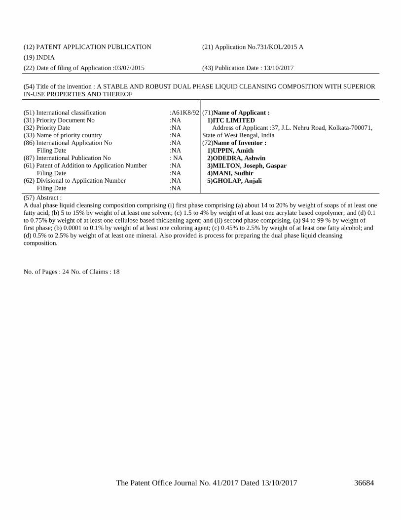
The Patent Office Journal No. 41/2017 Dated 13/10/2017 36684
(12) PATENT APPLICATION PUBLICATION (21) Application No.731/KOL/2015 A
(19) INDIA
(22) Date of filing of Application :03/07/2015 (43) Publication Date : 13/10/2017
(54) Title of the invention : A STABLE AND ROBUST DUAL PHASE LIQUID CLEANSING COMPOSITION WITH SUPERIOR
IN-USE PROPERTIES AND THEREOF
(51) International classification :A61K8/92
(31) Priority Document No :NA
(32) Priority Date :NA
(33) Name of priority country :NA
(86) International Application No
Filing Date
:NA
:NA
(87) International Publication No : NA
(61) Patent of Addition to Application Number
Filing Date
:NA
:NA
(62) Divisional to Application Number
Filing Date
:NA
:NA
(71)Name of Applicant :
1)ITC LIMITED Address of Applicant :37, J.L. Nehru Road, Kolkata-700071,
State of West Bengal, India
(72)Name of Inventor :
1)UPPIN, Amith
2)ODEDRA, Ashwin
3)MILTON, Joseph, Gaspar
4)MANI, Sudhir
5)GHOLAP, Anjali
(57) Abstract :
A dual phase liquid cleansing composition comprising (i) first phase comprising (a) about 14 to 20% by weight of soaps of at least one
fatty acid; (b) 5 to 15% by weight of at least one solvent; (c) 1.5 to 4% by weight of at least one acrylate based copolymer; and (d) 0.1
to 0.75% by weight of at least one cellulose based thickening agent; and (ii) second phase comprising, (a) 94 to 99 % by weight of
first phase; (b) 0.0001 to 0.1% by weight of at least one coloring agent; (c) 0.45% to 2.5% by weight of at least one fatty alcohol; and
(d) 0.5% to 2.5% by weight of at least one mineral. Also provided is process for preparing the dual phase liquid cleansing
composition.
No. of Pages : 24 No. of Claims : 18
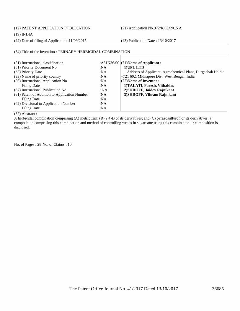
The Patent Office Journal No. 41/2017 Dated 13/10/2017 36685
(12) PATENT APPLICATION PUBLICATION (21) Application No.972/KOL/2015 A
(19) INDIA
(22) Date of filing of Application :11/09/2015 (43) Publication Date : 13/10/2017
(54) Title of the invention : TERNARY HERBICIDAL COMBINATION
(51) International classification :A61K36/00
(31) Priority Document No :NA
(32) Priority Date :NA
(33) Name of priority country :NA
(86) International Application No
Filing Date
:NA
:NA
(87) International Publication No : NA
(61) Patent of Addition to Application Number
Filing Date
:NA
:NA
(62) Divisional to Application Number
Filing Date
:NA
:NA
(71)Name of Applicant :
1)UPL LTD Address of Applicant :Agrochemical Plant, Durgachak Haldia
–721 602, Midnapore Dist. West Bengal, India
(72)Name of Inventor :
1)TALATI, Paresh, Vithaldas
2)SHROFF, Jaidev Rajnikant
3)SHROFF, Vikram Rajnikant
(57) Abstract :
A herbicidal combination comprising (A) metribuzin; (B) 2,4-D or its derivatives; and (C) pyrazosulfuron or its derivatives, a
composition comprising this combination and method of controlling weeds in sugarcane using this combination or composition is
disclosed.
No. of Pages : 28 No. of Claims : 10
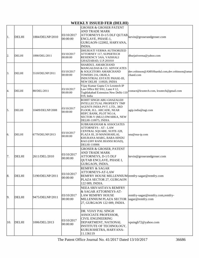
The Patent Office Journal No. 41/2017 Dated 13/10/2017 36686
WEEKLY ISSUED FER (DELHI)
1. DELHI 1884/DELNP/2010 03/10/2017
00:00:00
GROSER & GROSER PATENT
AND TRADE MARK
ATTORNEYS D-1/5 DLF QUTAB
ENCLAVE, PHASE-1,
GURGAON-122002, HARYANA,
INDIA.
2. DELHI 1890/DEL/2011 03/10/2017
00:00:00
DHURJATI VERMA AUTHORIZED
ATTORNEY 117, SUPERTECH
RESIDENCY 5/6A, VAISHALI
GHAZIABAD, U.P.201010
3. DELHI 5518/DELNP/2011 03/10/2017
00:00:00
SHARDUL AMARCHAND
MANGALDAS & CO. ADVOCATES
& SOLICITORS AMARCHAND
TOWERS 216, OKHLA
INDUSTRIAL ESTATE PHASE-III,
NEW DELHI 110020, INDIA
[email protected],dev.robinson@amar
chand.com
4. DELHI 88/DEL/2011 03/10/2017
00:00:00
Vijay Kumar Gupta C/o Lexntech IP
Law Office RZ 9/61, Lane # 12,
Tughlakabad Extension New Delhi-110
019, India
[email protected], [email protected]
5. DELHI 10409/DELNP/2008 03/10/2017
00:00:00
ROHIT SINGH ABU-GHAZALEH
INTELLECTUAL PROPERTY TMP
AGENTS INDIA PVT. LTD., 3RD
FLOOR, H.L. ARCADE, NEAR
HDFC BANK, PLOT NO.14,
SECTOR-V (MLU) DWARKA, NEW
DELHI-110075, INDIA.
6. DELHI 6779/DELNP/2013 03/10/2017
00:00:00
SUBRAMANIAM & ASSOCIATES
ATTORNEYS - AT - LAW
CENTRAL SQUARE, SUITE-328,
PLAZA III, 20 MANOHARLAL
KHURANA MARG, BARA HINDU
RAO (OFF RANI JHANSI ROAD),
DELHI-110006
7. DELHI 2611/DEL/2010 03/10/2017
00:00:00
GROSER & GROSER, PATENT
AND TRADE MARK
ATTORNEYS, D-1/5 DLF
QUTAB ENCLAVE, PHASE I,
GURGAON, INDIA.
8. DELHI 5190/DELNP/2011 03/10/2017
00:00:00
REMFRY & SAGAR
ATTORNEYS-AT-LAW
REMFRY HOUSE MILLENNIUM
PLAZA SECTOR 27, GURGAON
122 009, INDIA.
9. DELHI 9475/DELNP/2011 03/10/2017
00:00:00
NEEA SRIVASTAVA REMFRY
& SAGAR ATTORNEYS-AT-
LAW REMFRY HOUSE
MILLENNIUM PLAZA SECTOR
27, GURGAON 122 009, INDIA.
[email protected],remfry-
10. DELHI 1006/DEL/2013 03/10/2017
00:00:00
DR. VIJAY PAL SINGH
ASSOCIATE PROFESSOR,
CIVIL ENGINEERING
DEPARTMENT, NATIONAL
INSTITUTE OF TECHNOLOGY,
KURUKSHETRA, HARYANA-
11.136119
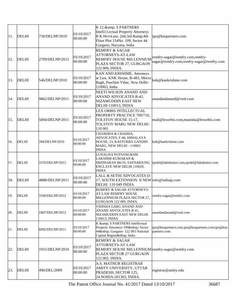
The Patent Office Journal No. 41/2017 Dated 13/10/2017 36687
11. DELHI 750/DELNP/2010 03/10/2017
00:00:00
K 12.& S PARTNERS
Intell13.ectual Property Attorneys
B K Ho14.use, 2nd,3rd &4th
Floor Plot 154No. 109, Sector 44
Gurgaon, Haryana, India
12. DELHI 2709/DELNP/2012 03/10/2017
00:00:00
REMFRY & SAGAR
ATTORNEYS-AT-LAW
REMFRY HOUSE MILLENNIUM
PLAZA SECTOR 27, GURGAON
122 009, INDIA.
[email protected],remfry-
[email protected],[email protected]
13. DELHI 546/DELNP/2010 03/10/2017
00:00:00
KAN AND KRISHME, Attorneys
at Law, KNK House, B-483, Meera
Bagh, Paschim Vihar, New Delhi-
110063, India
14. DELHI 9862/DELNP/2011 03/10/2017
00:00:00
NEETI WILSON ANAND AND
ANAND ADVOCATES B-41,
NIZAMUDDIN EAST NEW
DELHI-110013, INDIA
15. DELHI 5004/DELNP/2011 03/10/2017
00:00:00
LEX ORBIS INTELLECTUAL
PROPERTY PRACTICE 709/710,
TOLSTOY HOUSE 15-17,
TOLSTOY MARG NEW DELHI-
110 001
[email protected],[email protected]
16. DELHI 394/DELNP/2010 03/10/2017
00:00:00
CHANDHA & CHADHA,
ADVOCATES, F-46, HIMALAYA
HOUSE, 23, KASTURBA GANDHI
MARG, NEW DELHI - 110001
INDIA.
17. DELHI 3376/DELNP/2012 03/10/2017
00:00:00
LUNALISA POTSANGBAM
LAKSHMI KUMARAN &
SRIDHARAN B6/10, SAFDARJUNG
ENCLAVE NEW DELHI 110029,
INDIA
[email protected],[email protected]
18. DELHI 4888/DELNP/2011 03/10/2017
00:00:00
LALL & SETHI ADVOCATES D-
17, SOUTH EXTENSION II NEW
DELHI 110 049 INDIA
19. DELHI 3100/DELNP/2012 03/10/2017
00:00:00
REMFRY & SAGAR ATTORNEYS-
AT-LAW REMFRY HOUSE
MILLENNIUM PLAZA SECTOR 27,
GURGAON 122 009, INDIA.
20. DELHI 1867/DELNP/2012 03/10/2017
00:00:00
VIDISHA GARG ANAND AND
ANAND ADVOCATES B-41,
NIZAMUDDIN EAST NEW DELHI
110013, INDIA
21. DELHI 6092/DELNP/2011 03/10/2017
00:00:00
K & S PARTNERS Intellectual
Property Attorneys 109 Sector
44 Gurgaon- 122 003 National
Capital Region India
[email protected],[email protected],ipo@kns
partners.com
22. DELHI 1931/DELNP/2010 03/10/2017
00:00:00
REMFRY & SAGAR
ATTORNEYS-AT-LAW
REMFRY HOUSE MILLENNIUM
PLAZA SECTOR 27 GURGAON
122 002, INDIA.
23. DELHI 496/DEL/2009 03/10/2017
00:00:00
A.S. MATHUR REGISTRAR
AMITY UNIVERSITY, UTTAR
PRADESH, SECTOR 125,
24.NOIDA-201303, INDIA.
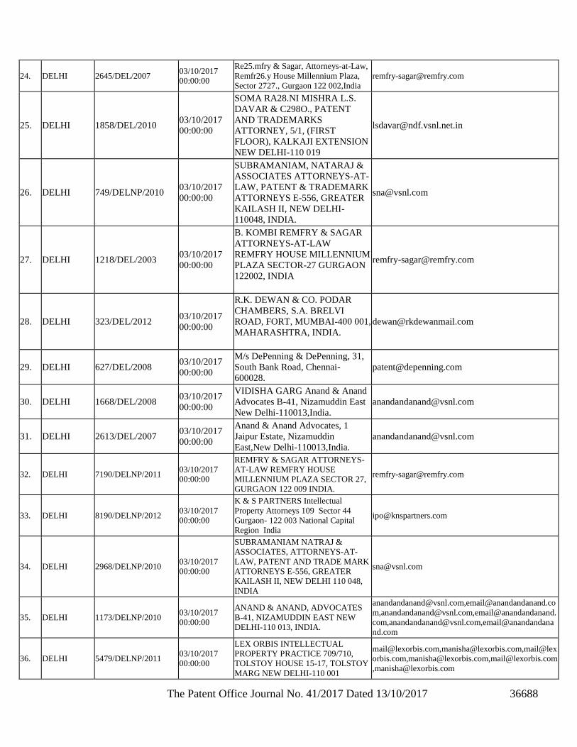
The Patent Office Journal No. 41/2017 Dated 13/10/2017 36688
24. DELHI 2645/DEL/2007 03/10/2017
00:00:00
Re25.mfry & Sagar, Attorneys-at-Law,
Remfr26.y House Millennium Plaza,
Sector 2727., Gurgaon 122 002,India
25. DELHI 1858/DEL/2010 03/10/2017
00:00:00
SOMA RA28.NI MISHRA L.S.
DAVAR & C298O., PATENT
AND TRADEMARKS
ATTORNEY, 5/1, (FIRST
FLOOR), KALKAJI EXTENSION
NEW DELHI-110 019
26. DELHI 749/DELNP/2010 03/10/2017
00:00:00
SUBRAMANIAM, NATARAJ &
ASSOCIATES ATTORNEYS-AT-
LAW, PATENT & TRADEMARK
ATTORNEYS E-556, GREATER
KAILASH II, NEW DELHI-
110048, INDIA.
27. DELHI 1218/DEL/2003 03/10/2017
00:00:00
B. KOMBI REMFRY & SAGAR
ATTORNEYS-AT-LAW
REMFRY HOUSE MILLENNIUM
PLAZA SECTOR-27 GURGAON
122002, INDIA
28. DELHI 323/DEL/2012 03/10/2017
00:00:00
R.K. DEWAN & CO. PODAR
CHAMBERS, S.A. BRELVI
ROAD, FORT, MUMBAI-400 001,
MAHARASHTRA, INDIA.
29. DELHI 627/DEL/2008 03/10/2017
00:00:00
M/s DePenning & DePenning, 31,
South Bank Road, Chennai-
600028.
30. DELHI 1668/DEL/2008 03/10/2017
00:00:00
VIDISHA GARG Anand & Anand
Advocates B-41, Nizamuddin East
New Delhi-110013,India.
31. DELHI 2613/DEL/2007 03/10/2017
00:00:00
Anand & Anand Advocates, 1
Jaipur Estate, Nizamuddin
East,New Delhi-110013,India.
32. DELHI 7190/DELNP/2011 03/10/2017
00:00:00
REMFRY & SAGAR ATTORNEYS-
AT-LAW REMFRY HOUSE
MILLENNIUM PLAZA SECTOR 27,
GURGAON 122 009 INDIA.
33. DELHI 8190/DELNP/2012 03/10/2017
00:00:00
K & S PARTNERS Intellectual
Property Attorneys 109 Sector 44
Gurgaon- 122 003 National Capital
Region India
34. DELHI 2968/DELNP/2010 03/10/2017
00:00:00
SUBRAMANIAM NATRAJ &
ASSOCIATES, ATTORNEYS-AT-
LAW, PATENT AND TRADE MARK
ATTORNEYS E-556, GREATER
KAILASH II, NEW DELHI 110 048,
INDIA
35. DELHI 1173/DELNP/2010 03/10/2017
00:00:00
ANAND & ANAND, ADVOCATES
B-41, NIZAMUDDIN EAST NEW
DELHI-110 013, INDIA.
[email protected],[email protected]
m,[email protected],email@anandandanand.
com,[email protected],email@anandandana
nd.com
36. DELHI 5479/DELNP/2011 03/10/2017
00:00:00
LEX ORBIS INTELLECTUAL
PROPERTY PRACTICE 709/710,
TOLSTOY HOUSE 15-17, TOLSTOY
MARG NEW DELHI-110 001
[email protected],[email protected],mail@lex
orbis.com,[email protected],[email protected]
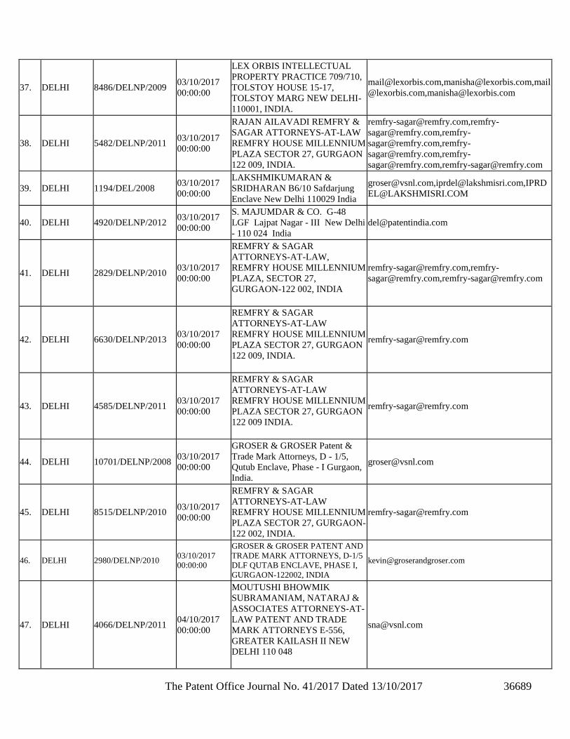
The Patent Office Journal No. 41/2017 Dated 13/10/2017 36689
37. DELHI 8486/DELNP/2009 03/10/2017
00:00:00
LEX ORBIS INTELLECTUAL
PROPERTY PRACTICE 709/710,
TOLSTOY HOUSE 15-17,
TOLSTOY MARG NEW DELHI-
110001, INDIA.
[email protected],[email protected],mail
@lexorbis.com,[email protected]
38. DELHI 5482/DELNP/2011 03/10/2017
00:00:00
RAJAN AILAVADI REMFRY &
SAGAR ATTORNEYS-AT-LAW
REMFRY HOUSE MILLENNIUM
PLAZA SECTOR 27, GURGAON
122 009, INDIA.
[email protected],remfry-
[email protected],remfry-
[email protected],remfry-
[email protected],remfry-
[email protected],[email protected]
39. DELHI 1194/DEL/2008 03/10/2017
00:00:00
LAKSHMIKUMARAN &
SRIDHARAN B6/10 Safdarjung
Enclave New Delhi 110029 India
[email protected],[email protected],IPRD
40. DELHI 4920/DELNP/2012 03/10/2017
00:00:00
S. MAJUMDAR & CO. G-48
LGF Lajpat Nagar - III New Delhi
- 110 024 India
41. DELHI 2829/DELNP/2010 03/10/2017
00:00:00
REMFRY & SAGAR
ATTORNEYS-AT-LAW,
REMFRY HOUSE MILLENNIUM
PLAZA, SECTOR 27,
GURGAON-122 002, INDIA
[email protected],remfry-
[email protected],[email protected]
42. DELHI 6630/DELNP/2013 03/10/2017
00:00:00
REMFRY & SAGAR
ATTORNEYS-AT-LAW
REMFRY HOUSE MILLENNIUM
PLAZA SECTOR 27, GURGAON
122 009, INDIA.
43. DELHI 4585/DELNP/2011 03/10/2017
00:00:00
REMFRY & SAGAR
ATTORNEYS-AT-LAW
REMFRY HOUSE MILLENNIUM
PLAZA SECTOR 27, GURGAON
122 009 INDIA.
44. DELHI 10701/DELNP/2008 03/10/2017
00:00:00
GROSER & GROSER Patent &
Trade Mark Attorneys, D - 1/5,
Qutub Enclave, Phase - I Gurgaon,
India.
45. DELHI 8515/DELNP/2010 03/10/2017
00:00:00
REMFRY & SAGAR
ATTORNEYS-AT-LAW
REMFRY HOUSE MILLENNIUM
PLAZA SECTOR 27, GURGAON-
122 002, INDIA.
46. DELHI 2980/DELNP/2010 03/10/2017
00:00:00
GROSER & GROSER PATENT AND
TRADE MARK ATTORNEYS, D-1/5
DLF QUTAB ENCLAVE, PHASE I,
GURGAON-122002, INDIA
47. DELHI 4066/DELNP/2011 04/10/2017
00:00:00
MOUTUSHI BHOWMIK
SUBRAMANIAM, NATARAJ &
ASSOCIATES ATTORNEYS-AT-
LAW PATENT AND TRADE
MARK ATTORNEYS E-556,
GREATER KAILASH II NEW
DELHI 110 048
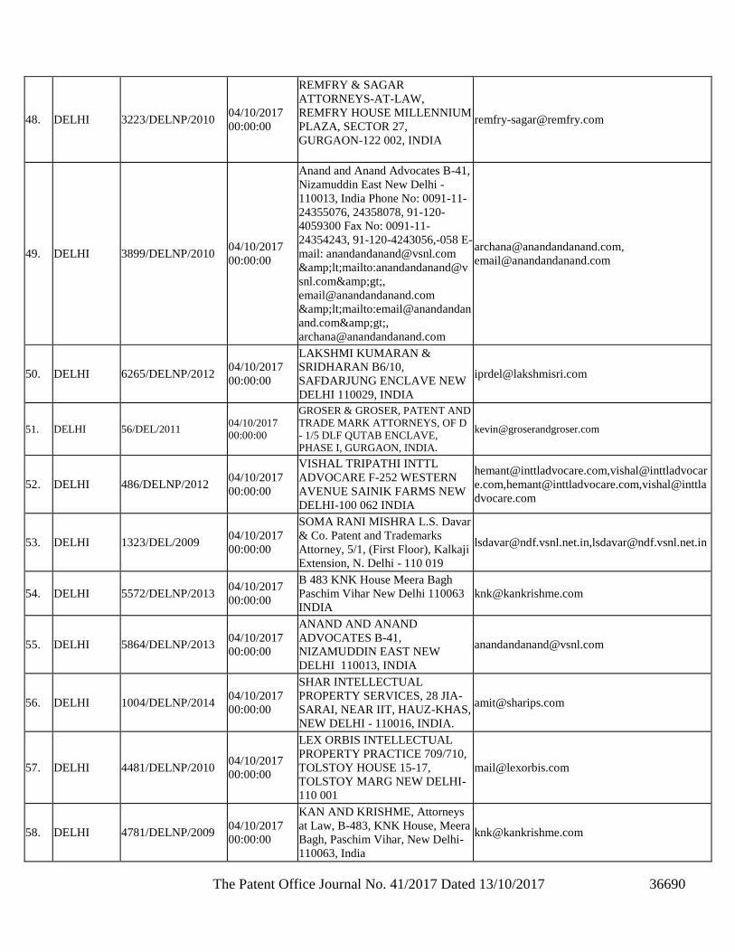
The Patent Office Journal No. 41/2017 Dated 13/10/2017 36690
48. DELHI 3223/DELNP/2010 04/10/2017
00:00:00
REMFRY & SAGAR
ATTORNEYS-AT-LAW,
REMFRY HOUSE MILLENNIUM
PLAZA, SECTOR 27,
GURGAON-122 002, INDIA
49. DELHI 3899/DELNP/2010 04/10/2017
00:00:00
Anand and Anand Advocates B-41,
Nizamuddin East New Delhi -
110013, India Phone No: 0091-11-
24355076, 24358078, 91-120-
4059300 Fax No: 0091-11-
24354243, 91-120-4243056,-058 E-
mail: [email protected]
&lt;mailto:anandandanand@v
snl.com&gt;,
&lt;mailto:email@anandandan
and.com&gt;,
50. DELHI 6265/DELNP/2012 04/10/2017
00:00:00
LAKSHMI KUMARAN &
SRIDHARAN B6/10,
SAFDARJUNG ENCLAVE NEW
DELHI 110029, INDIA
51. DELHI 56/DEL/2011 04/10/2017
00:00:00
GROSER & GROSER, PATENT AND
TRADE MARK ATTORNEYS, OF D
- 1/5 DLF QUTAB ENCLAVE,
PHASE I, GURGAON, INDIA.
52. DELHI 486/DELNP/2012 04/10/2017
00:00:00
VISHAL TRIPATHI INTTL
ADVOCARE F-252 WESTERN
AVENUE SAINIK FARMS NEW
DELHI-100 062 INDIA
[email protected],vishal@inttladvocar
e.com,[email protected],vishal@inttla
dvocare.com
53. DELHI 1323/DEL/2009 04/10/2017
00:00:00
SOMA RANI MISHRA L.S. Davar
& Co. Patent and Trademarks
Attorney, 5/1, (First Floor), Kalkaji
Extension, N. Delhi - 110 019
[email protected],[email protected]
54. DELHI 5572/DELNP/2013 04/10/2017
00:00:00
B 483 KNK House Meera Bagh
Paschim Vihar New Delhi 110063
INDIA
55. DELHI 5864/DELNP/2013 04/10/2017
00:00:00
ANAND AND ANAND
ADVOCATES B-41,
NIZAMUDDIN EAST NEW
DELHI 110013, INDIA
56. DELHI 1004/DELNP/2014 04/10/2017
00:00:00
SHAR INTELLECTUAL
PROPERTY SERVICES, 28 JIA-
SARAI, NEAR IIT, HAUZ-KHAS,
NEW DELHI - 110016, INDIA.
57. DELHI 4481/DELNP/2010 04/10/2017
00:00:00
LEX ORBIS INTELLECTUAL
PROPERTY PRACTICE 709/710,
TOLSTOY HOUSE 15-17,
TOLSTOY MARG NEW DELHI-
110 001
58. DELHI 4781/DELNP/2009 04/10/2017
00:00:00
KAN AND KRISHME, Attorneys
at Law, B-483, KNK House, Meera
Bagh, Paschim Vihar, New Delhi-
110063, India
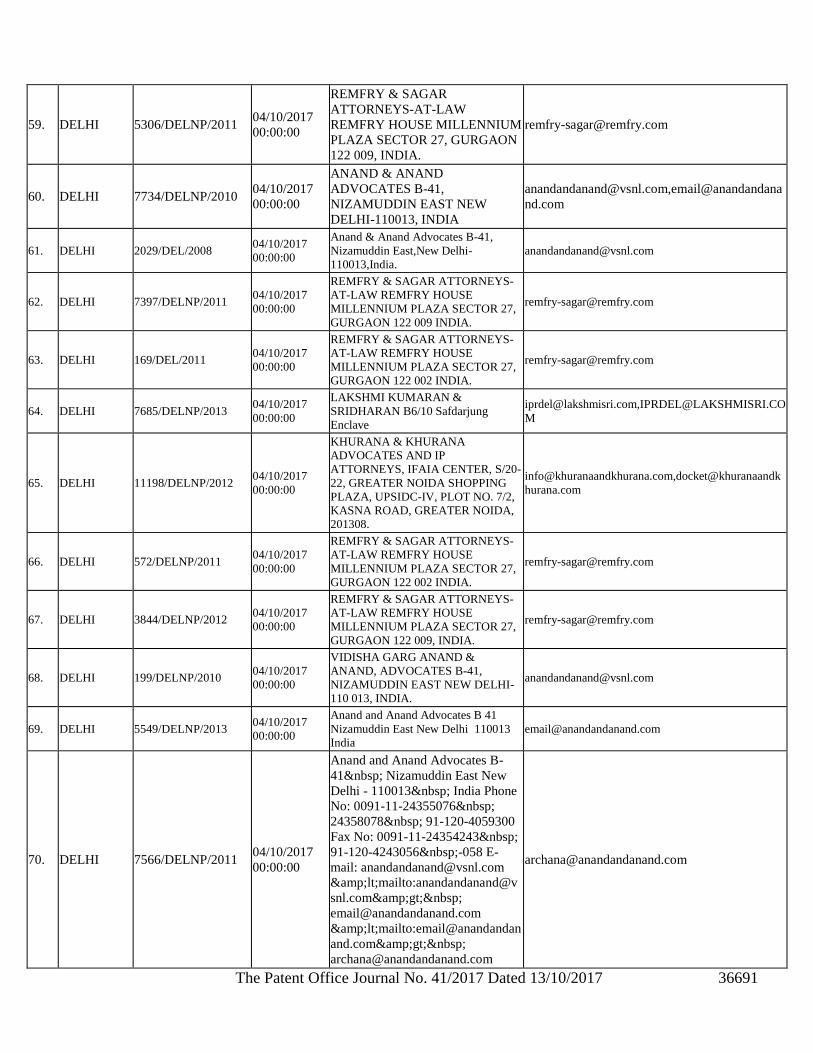
The Patent Office Journal No. 41/2017 Dated 13/10/2017 36691
59. DELHI 5306/DELNP/2011 04/10/2017
00:00:00
REMFRY & SAGAR
ATTORNEYS-AT-LAW
REMFRY HOUSE MILLENNIUM
PLAZA SECTOR 27, GURGAON
122 009, INDIA.
60. DELHI 7734/DELNP/2010 04/10/2017
00:00:00
ANAND & ANAND
ADVOCATES B-41,
NIZAMUDDIN EAST NEW
DELHI-110013, INDIA
[email protected],email@anandandana
nd.com
61. DELHI 2029/DEL/2008 04/10/2017
00:00:00
Anand & Anand Advocates B-41,
Nizamuddin East,New Delhi-
110013,India.
62. DELHI 7397/DELNP/2011 04/10/2017
00:00:00
REMFRY & SAGAR ATTORNEYS-
AT-LAW REMFRY HOUSE
MILLENNIUM PLAZA SECTOR 27,
GURGAON 122 009 INDIA.
63. DELHI 169/DEL/2011 04/10/2017
00:00:00
REMFRY & SAGAR ATTORNEYS-
AT-LAW REMFRY HOUSE
MILLENNIUM PLAZA SECTOR 27,
GURGAON 122 002 INDIA.
64. DELHI 7685/DELNP/2013 04/10/2017
00:00:00
LAKSHMI KUMARAN &
SRIDHARAN B6/10 Safdarjung
Enclave
[email protected],[email protected]
M
65. DELHI 11198/DELNP/2012 04/10/2017
00:00:00
KHURANA & KHURANA
ADVOCATES AND IP
ATTORNEYS, IFAIA CENTER, S/20-
22, GREATER NOIDA SHOPPING
PLAZA, UPSIDC-IV, PLOT NO. 7/2,
KASNA ROAD, GREATER NOIDA,
201308.
[email protected],docket@khuranaandk
hurana.com
66. DELHI 572/DELNP/2011 04/10/2017
00:00:00
REMFRY & SAGAR ATTORNEYS-
AT-LAW REMFRY HOUSE
MILLENNIUM PLAZA SECTOR 27,
GURGAON 122 002 INDIA.
67. DELHI 3844/DELNP/2012 04/10/2017
00:00:00
REMFRY & SAGAR ATTORNEYS-
AT-LAW REMFRY HOUSE
MILLENNIUM PLAZA SECTOR 27,
GURGAON 122 009, INDIA.
68. DELHI 199/DELNP/2010 04/10/2017
00:00:00
VIDISHA GARG ANAND &
ANAND, ADVOCATES B-41,
NIZAMUDDIN EAST NEW DELHI-
110 013, INDIA.
69. DELHI 5549/DELNP/2013 04/10/2017
00:00:00
Anand and Anand Advocates B 41
Nizamuddin East New Delhi 110013
India
70. DELHI 7566/DELNP/2011 04/10/2017
00:00:00
Anand and Anand Advocates B-
41 Nizamuddin East New
Delhi - 110013 India Phone
No: 0091-11-24355076
24358078 91-120-4059300
Fax No: 0091-11-24354243
91-120-4243056 -058 E-
mail: [email protected]
&lt;mailto:anandandanand@v
snl.com&gt;
&lt;mailto:email@anandandan
and.com&gt;
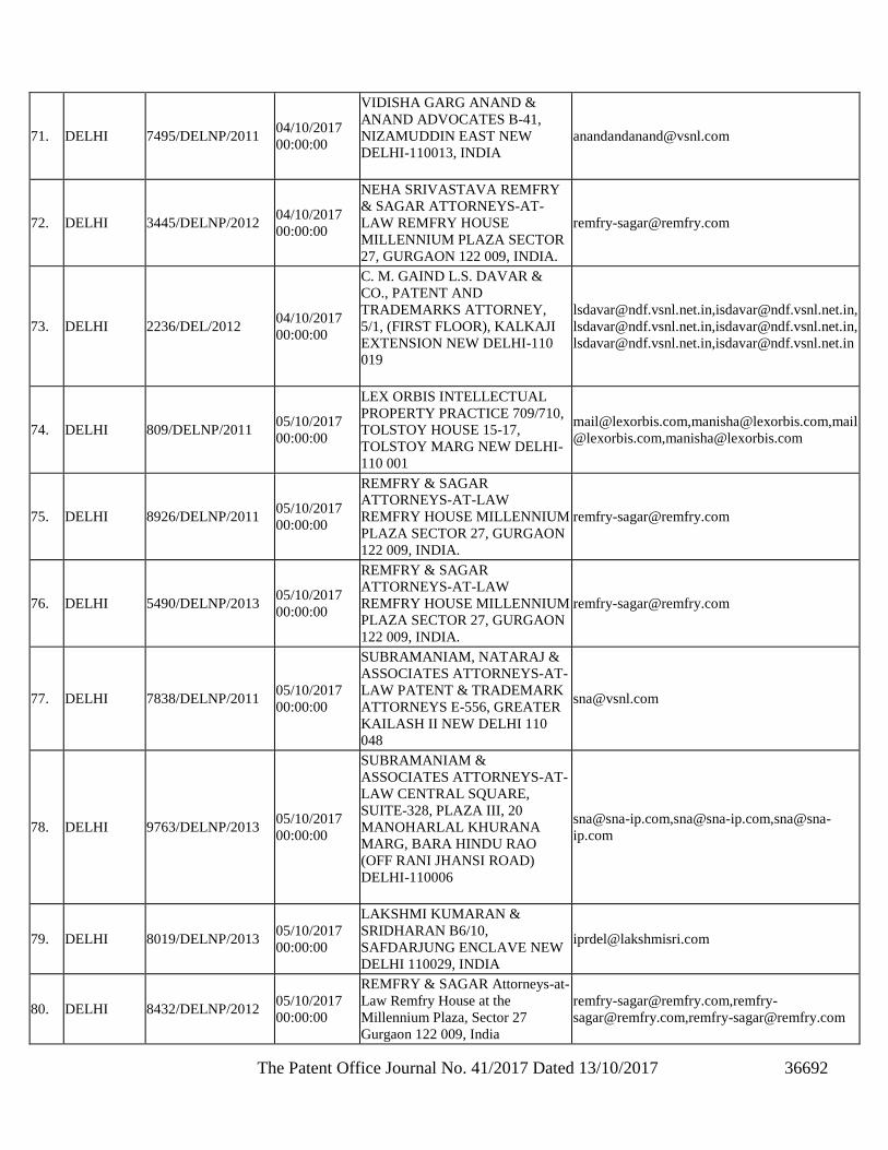
The Patent Office Journal No. 41/2017 Dated 13/10/2017 36692
71. DELHI 7495/DELNP/2011 04/10/2017
00:00:00
VIDISHA GARG ANAND &
ANAND ADVOCATES B-41,
NIZAMUDDIN EAST NEW
DELHI-110013, INDIA
72. DELHI 3445/DELNP/2012 04/10/2017
00:00:00
NEHA SRIVASTAVA REMFRY
& SAGAR ATTORNEYS-AT-
LAW REMFRY HOUSE
MILLENNIUM PLAZA SECTOR
27, GURGAON 122 009, INDIA.
73. DELHI 2236/DEL/2012 04/10/2017
00:00:00
C. M. GAIND L.S. DAVAR &
CO., PATENT AND
TRADEMARKS ATTORNEY,
5/1, (FIRST FLOOR), KALKAJI
EXTENSION NEW DELHI-110
019
[email protected],[email protected],
[email protected],[email protected],
[email protected],[email protected]
74. DELHI 809/DELNP/2011 05/10/2017
00:00:00
LEX ORBIS INTELLECTUAL
PROPERTY PRACTICE 709/710,
TOLSTOY HOUSE 15-17,
TOLSTOY MARG NEW DELHI-
110 001
[email protected],[email protected],mail
@lexorbis.com,[email protected]
75. DELHI 8926/DELNP/2011 05/10/2017
00:00:00
REMFRY & SAGAR
ATTORNEYS-AT-LAW
REMFRY HOUSE MILLENNIUM
PLAZA SECTOR 27, GURGAON
122 009, INDIA.
76. DELHI 5490/DELNP/2013 05/10/2017
00:00:00
REMFRY & SAGAR
ATTORNEYS-AT-LAW
REMFRY HOUSE MILLENNIUM
PLAZA SECTOR 27, GURGAON
122 009, INDIA.
77. DELHI 7838/DELNP/2011 05/10/2017
00:00:00
SUBRAMANIAM, NATARAJ &
ASSOCIATES ATTORNEYS-AT-
LAW PATENT & TRADEMARK
ATTORNEYS E-556, GREATER
KAILASH II NEW DELHI 110
048
78. DELHI 9763/DELNP/2013 05/10/2017
00:00:00
SUBRAMANIAM &
ASSOCIATES ATTORNEYS-AT-
LAW CENTRAL SQUARE,
SUITE-328, PLAZA III, 20
MANOHARLAL KHURANA
MARG, BARA HINDU RAO
(OFF RANI JHANSI ROAD)
DELHI-110006
[email protected],[email protected],sna@sna-
ip.com
79. DELHI 8019/DELNP/2013 05/10/2017
00:00:00
LAKSHMI KUMARAN &
SRIDHARAN B6/10,
SAFDARJUNG ENCLAVE NEW
DELHI 110029, INDIA
80. DELHI 8432/DELNP/2012 05/10/2017
00:00:00
REMFRY & SAGAR Attorneys-at-
Law Remfry House at the
Millennium Plaza, Sector 27
Gurgaon 122 009, India
[email protected],remfry-
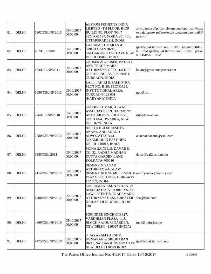
The Patent Office Journal No. 41/2017 Dated 13/10/2017 36693
81. DELHI 5302/DELNP/2013 05/10/2017
00:00:00
ALSTOM PROJECTS INDIA
LIMITED 4TH FLOOR, IHDP
BUILDING, PLOT NO. 7
SECTOR 127, NOIDA 201 301,
UTTARPRADESH, INDIA
[email protected],[email protected]
om,[email protected],bpo.mail@
ge.com
82. DELHI 437/DEL/2008 05/10/2017
00:00:00
LAKSHMIKUMARAN &
SRIDHARAN B6/10,
SAFDARJUNG ENCLAVE NEW
DELHI 110029, INDIA
[email protected],IPRDEL@LAKSHMIS
RI.COM,[email protected],IPRDEL@LA
KSHMISRI.COM
83. DELHI 163/DELNP/2011 05/10/2017
00:00:00
GROSER & GROSER, PATENT
AND TRADE MARK
ATTORNEYS, OF D - 1/5 DLF
QUTAB ENCLAVE, PHASE I,
GURGAON, INDIA.
84. DELHI 1656/DELNP/2013 05/10/2017
00:00:00
LALL LAHIRI & SALHOTRA
PLOT NO. B-28, SECTOR32,
INSTITUTIONAL AREA,
GURGAON-122 001
(HARYANA) INDIA
85. DELHI 726/DELNP/2010 05/10/2017
00:00:00
SUDHIR KUMAR, ASWAL
ASSOCIATES, 59, HARMONY
APARTMENTS, POCKET-1,
SECTOR-4, DWARKA, NEW
DELHI-78, INDIA
86. DELHI 2580/DELNP/2012 05/10/2017
00:00:00
ARPITA KULSHRESHTA
ANAND AND ANAND
ADVOCATES B-41,
NIZAMUDDIN EAST NEW
DELHI 110013, INDIA
87. DELHI 1588/DEL/2011 05/10/2017
00:00:00
MONA SAINI L.S. DAVAR &
CO. 32, RADHA MADHAB
DUTTA GARDEN LANE
KOLKATA-700010
88. DELHI 4114/DELNP/2012 05/10/2017
00:00:00
REMFRY & SAGAR
ATTORNEYS-AT-LAW
REMFRY HOUSE MILLENNIUM
PLAZA SECTOR 27, GURGAON
122 009, INDIA.
89. DELHI 1408/DELNP/2012 05/10/2017
00:00:00
SUBRAMANIAM, NATARAJ &
ASSOCIATES ATTORNEYS-AT-
LAW PATENT & TRADEMARK
ATTORNEYS E-556, GREATER
KAILASH II NEW DELHI 110
048
90. DELHI 4969/DELNP/2010 05/10/2017
00:00:00
SURINDER SINGH C/O 317,
VARDHMAN PLAZA -1, J.
BLOCK RAJOURI GARDEN,
NEW DELHI - 110027 (INDIA)
91. DELHI 4475/DELNP/2010 05/10/2017
00:00:00
S. JAYARAM LAKSHMI
KUMARAN & SRIDHARAN
B6/10, SAFDARJUNG ENCLAVE
NEW DELHI 110029 INDIA
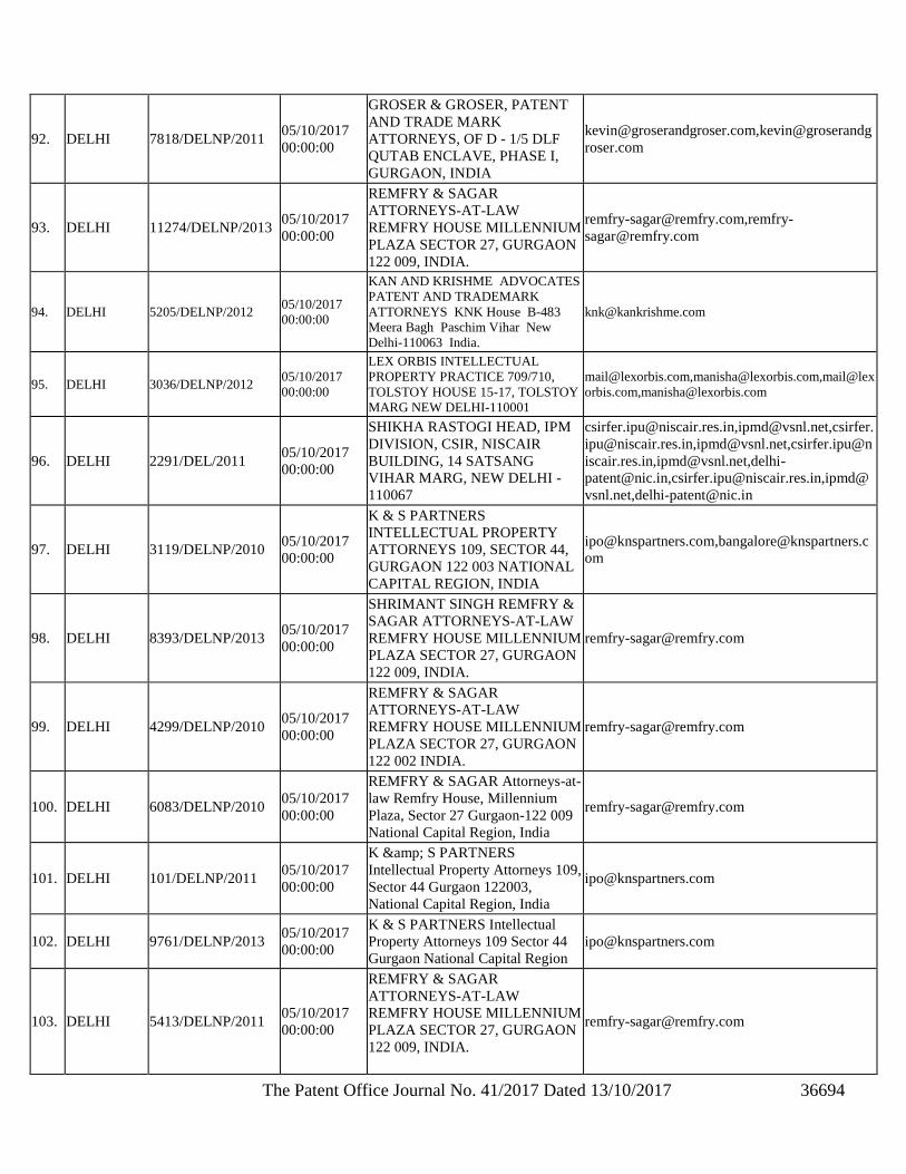
The Patent Office Journal No. 41/2017 Dated 13/10/2017 36694
92. DELHI 7818/DELNP/2011 05/10/2017
00:00:00
GROSER & GROSER, PATENT
AND TRADE MARK
ATTORNEYS, OF D - 1/5 DLF
QUTAB ENCLAVE, PHASE I,
GURGAON, INDIA
[email protected],kevin@groserandg
roser.com
93. DELHI 11274/DELNP/2013 05/10/2017
00:00:00
REMFRY & SAGAR
ATTORNEYS-AT-LAW
REMFRY HOUSE MILLENNIUM
PLAZA SECTOR 27, GURGAON
122 009, INDIA.
[email protected],remfry-
94. DELHI 5205/DELNP/2012 05/10/2017
00:00:00
KAN AND KRISHME ADVOCATES
PATENT AND TRADEMARK
ATTORNEYS KNK House B-483
Meera Bagh Paschim Vihar New
Delhi-110063 India.
95. DELHI 3036/DELNP/2012 05/10/2017
00:00:00
LEX ORBIS INTELLECTUAL
PROPERTY PRACTICE 709/710,
TOLSTOY HOUSE 15-17, TOLSTOY
MARG NEW DELHI-110001
[email protected],[email protected],mail@lex
orbis.com,[email protected]
96. DELHI 2291/DEL/2011 05/10/2017
00:00:00
SHIKHA RASTOGI HEAD, IPM
DIVISION, CSIR, NISCAIR
BUILDING, 14 SATSANG
VIHAR MARG, NEW DELHI -
110067
[email protected],[email protected],csirfer.
[email protected],[email protected],csirfer.ipu@n
iscair.res.in,[email protected],delhi-
[email protected],[email protected],ipmd@
vsnl.net,[email protected]
97. DELHI 3119/DELNP/2010 05/10/2017
00:00:00
K & S PARTNERS
INTELLECTUAL PROPERTY
ATTORNEYS 109, SECTOR 44,
GURGAON 122 003 NATIONAL
CAPITAL REGION, INDIA
[email protected],[email protected]
om
98. DELHI 8393/DELNP/2013 05/10/2017
00:00:00
SHRIMANT SINGH REMFRY &
SAGAR ATTORNEYS-AT-LAW
REMFRY HOUSE MILLENNIUM
PLAZA SECTOR 27, GURGAON
122 009, INDIA.
99. DELHI 4299/DELNP/2010 05/10/2017
00:00:00
REMFRY & SAGAR
ATTORNEYS-AT-LAW
REMFRY HOUSE MILLENNIUM
PLAZA SECTOR 27, GURGAON
122 002 INDIA.
100. DELHI 6083/DELNP/2010 05/10/2017
00:00:00
REMFRY & SAGAR Attorneys-at-
law Remfry House, Millennium
Plaza, Sector 27 Gurgaon-122 009
National Capital Region, India
101. DELHI 101/DELNP/2011 05/10/2017
00:00:00
K & S PARTNERS
Intellectual Property Attorneys 109,
Sector 44 Gurgaon 122003,
National Capital Region, India
102. DELHI 9761/DELNP/2013 05/10/2017
00:00:00
K & S PARTNERS Intellectual
Property Attorneys 109 Sector 44
Gurgaon National Capital Region
103. DELHI 5413/DELNP/2011 05/10/2017
00:00:00
REMFRY & SAGAR
ATTORNEYS-AT-LAW
REMFRY HOUSE MILLENNIUM
PLAZA SECTOR 27, GURGAON
122 009, INDIA.
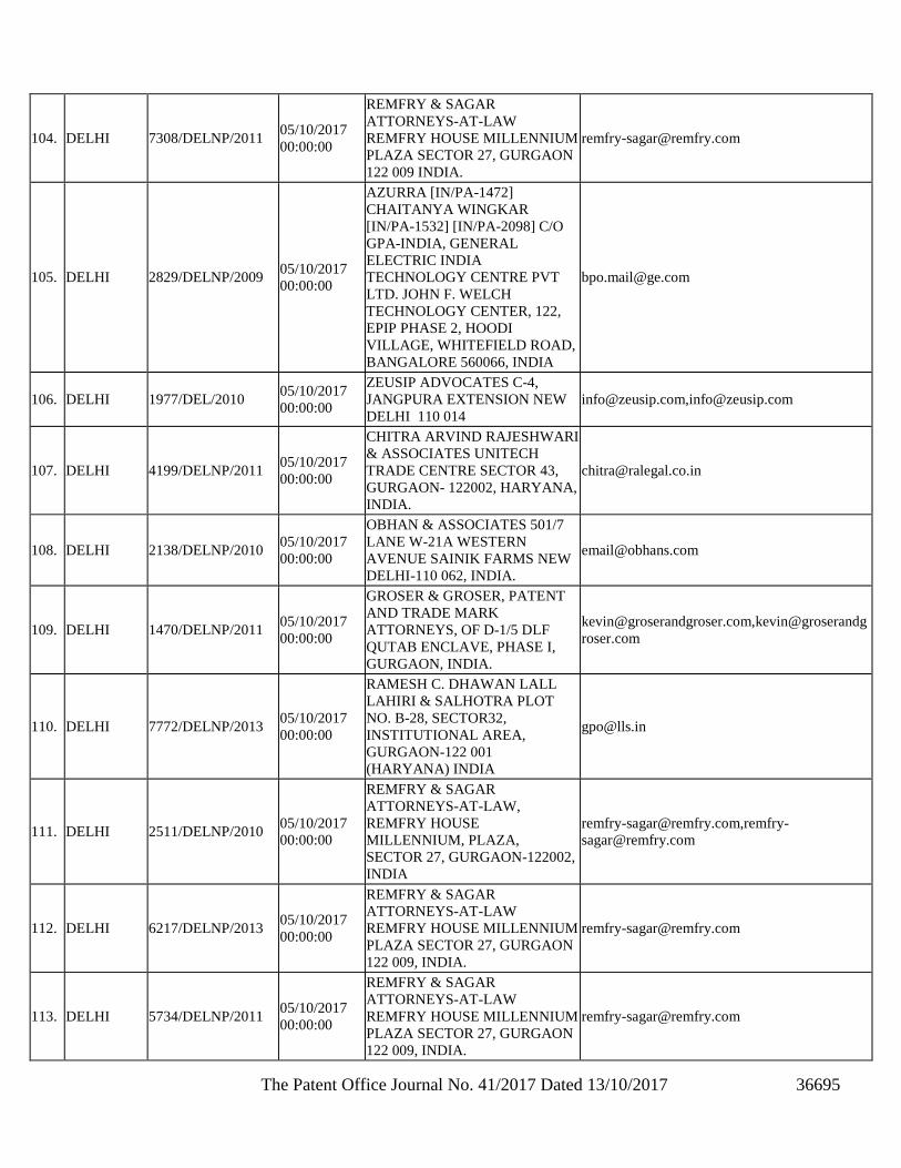
The Patent Office Journal No. 41/2017 Dated 13/10/2017 36695
104. DELHI 7308/DELNP/2011 05/10/2017
00:00:00
REMFRY & SAGAR
ATTORNEYS-AT-LAW
REMFRY HOUSE MILLENNIUM
PLAZA SECTOR 27, GURGAON
122 009 INDIA.
105. DELHI 2829/DELNP/2009 05/10/2017
00:00:00
AZURRA [IN/PA-1472]
CHAITANYA WINGKAR
[IN/PA-1532] [IN/PA-2098] C/O
GPA-INDIA, GENERAL
ELECTRIC INDIA
TECHNOLOGY CENTRE PVT
LTD. JOHN F. WELCH
TECHNOLOGY CENTER, 122,
EPIP PHASE 2, HOODI
VILLAGE, WHITEFIELD ROAD,
BANGALORE 560066, INDIA
106. DELHI 1977/DEL/2010 05/10/2017
00:00:00
ZEUSIP ADVOCATES C-4,
JANGPURA EXTENSION NEW
DELHI 110 014
[email protected],[email protected]
107. DELHI 4199/DELNP/2011 05/10/2017
00:00:00
CHITRA ARVIND RAJESHWARI
& ASSOCIATES UNITECH
TRADE CENTRE SECTOR 43,
GURGAON- 122002, HARYANA,
INDIA.
108. DELHI 2138/DELNP/2010 05/10/2017
00:00:00
OBHAN & ASSOCIATES 501/7
LANE W-21A WESTERN
AVENUE SAINIK FARMS NEW
DELHI-110 062, INDIA.
109. DELHI 1470/DELNP/2011 05/10/2017
00:00:00
GROSER & GROSER, PATENT
AND TRADE MARK
ATTORNEYS, OF D-1/5 DLF
QUTAB ENCLAVE, PHASE I,
GURGAON, INDIA.
[email protected],kevin@groserandg
roser.com
110. DELHI 7772/DELNP/2013 05/10/2017
00:00:00
RAMESH C. DHAWAN LALL
LAHIRI & SALHOTRA PLOT
NO. B-28, SECTOR32,
INSTITUTIONAL AREA,
GURGAON-122 001
(HARYANA) INDIA
111. DELHI 2511/DELNP/2010 05/10/2017
00:00:00
REMFRY & SAGAR
ATTORNEYS-AT-LAW,
REMFRY HOUSE
MILLENNIUM, PLAZA,
SECTOR 27, GURGAON-122002,
INDIA
[email protected],remfry-
112. DELHI 6217/DELNP/2013 05/10/2017
00:00:00
REMFRY & SAGAR
ATTORNEYS-AT-LAW
REMFRY HOUSE MILLENNIUM
PLAZA SECTOR 27, GURGAON
122 009, INDIA.
113. DELHI 5734/DELNP/2011 05/10/2017
00:00:00
REMFRY & SAGAR
ATTORNEYS-AT-LAW
REMFRY HOUSE MILLENNIUM
PLAZA SECTOR 27, GURGAON
122 009, INDIA.
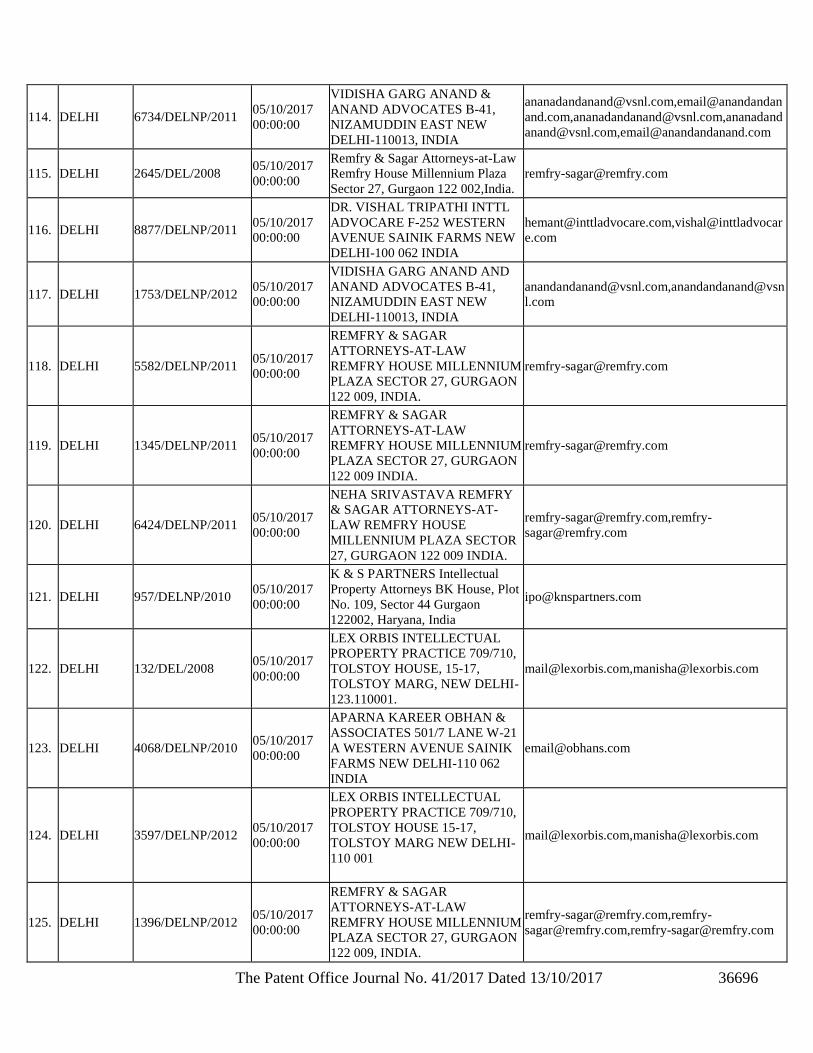
The Patent Office Journal No. 41/2017 Dated 13/10/2017 36696
114. DELHI 6734/DELNP/2011 05/10/2017
00:00:00
VIDISHA GARG ANAND &
ANAND ADVOCATES B-41,
NIZAMUDDIN EAST NEW
DELHI-110013, INDIA
[email protected],email@anandandan
and.com,[email protected],ananadand
[email protected],[email protected]
115. DELHI 2645/DEL/2008 05/10/2017
00:00:00
Remfry & Sagar Attorneys-at-Law
Remfry House Millennium Plaza
Sector 27, Gurgaon 122 002,India.
116. DELHI 8877/DELNP/2011 05/10/2017
00:00:00
DR. VISHAL TRIPATHI INTTL
ADVOCARE F-252 WESTERN
AVENUE SAINIK FARMS NEW
DELHI-100 062 INDIA
[email protected],vishal@inttladvocar
e.com
117. DELHI 1753/DELNP/2012 05/10/2017
00:00:00
VIDISHA GARG ANAND AND
ANAND ADVOCATES B-41,
NIZAMUDDIN EAST NEW
DELHI-110013, INDIA
[email protected],anandandanand@vsn
l.com
118. DELHI 5582/DELNP/2011 05/10/2017
00:00:00
REMFRY & SAGAR
ATTORNEYS-AT-LAW
REMFRY HOUSE MILLENNIUM
PLAZA SECTOR 27, GURGAON
122 009, INDIA.
119. DELHI 1345/DELNP/2011 05/10/2017
00:00:00
REMFRY & SAGAR
ATTORNEYS-AT-LAW
REMFRY HOUSE MILLENNIUM
PLAZA SECTOR 27, GURGAON
122 009 INDIA.
120. DELHI 6424/DELNP/2011 05/10/2017
00:00:00
NEHA SRIVASTAVA REMFRY
& SAGAR ATTORNEYS-AT-
LAW REMFRY HOUSE
MILLENNIUM PLAZA SECTOR
27, GURGAON 122 009 INDIA.
[email protected],remfry-
121. DELHI 957/DELNP/2010 05/10/2017
00:00:00
K & S PARTNERS Intellectual
Property Attorneys BK House, Plot
No. 109, Sector 44 Gurgaon
122002, Haryana, India
122. DELHI 132/DEL/2008 05/10/2017
00:00:00
LEX ORBIS INTELLECTUAL
PROPERTY PRACTICE 709/710,
TOLSTOY HOUSE, 15-17,
TOLSTOY MARG, NEW DELHI-
123.110001.
[email protected],[email protected]
123. DELHI 4068/DELNP/2010 05/10/2017
00:00:00
APARNA KAREER OBHAN &
ASSOCIATES 501/7 LANE W-21
A WESTERN AVENUE SAINIK
FARMS NEW DELHI-110 062
INDIA
124. DELHI 3597/DELNP/2012 05/10/2017
00:00:00
LEX ORBIS INTELLECTUAL
PROPERTY PRACTICE 709/710,
TOLSTOY HOUSE 15-17,
TOLSTOY MARG NEW DELHI-
110 001
[email protected],[email protected]
125. DELHI 1396/DELNP/2012 05/10/2017
00:00:00
REMFRY & SAGAR
ATTORNEYS-AT-LAW
REMFRY HOUSE MILLENNIUM
PLAZA SECTOR 27, GURGAON
122 009, INDIA.
[email protected],remfry-
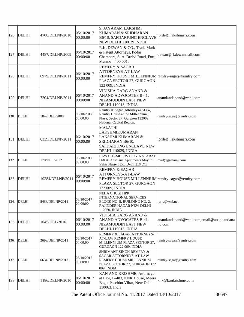
The Patent Office Journal No. 41/2017 Dated 13/10/2017 36697
126. DELHI 4700/DELNP/2010 05/10/2017
00:00:00
S. JAYARAM LAKSHMI
KUMARAN & SRIDHARAN
B6/10, SAFDARJUNG ENCLAVE
NEW DELHI 110029 INDIA
127. DELHI 4487/DELNP/2009 06/10/2017
00:00:00
R.K. DEWAN & CO., Trade Mark
& Patent Attorneys, Podar
Chambers, S. A. Brelvi Road, Fort,
Mumbai 400 001.
128. DELHI 6979/DELNP/2011 06/10/2017
00:00:00
REMFRY & SAGAR
ATTORNEYS-AT-LAW
REMFRY HOUSE MILLENNIUM
PLAZA SECTOR 27, GURGAON
122 009, INDIA
129. DELHI 7204/DELNP/2011 06/10/2017
00:00:00
VIDISHA GARG ANAND &
ANAND ADVOCATES B-41,
NIZAMUDDIN EAST NEW
DELHI-110013, INDIA
130. DELHI 1849/DEL/2008 06/10/2017
00:00:00
Remfry & Sagar, Attorneys-at-Law,
Remfry House at the Millennium,
Plaza, Sector 27, Gurgaon 122002,
National Capital Region.
131. DELHI 6339/DELNP/2011 06/10/2017
00:00:00
MALATHI
LAKSHMIKUMARAN
LAKSHMI KUMARAN &
SRIDHARAN B6/10,
SAFDARJUNG ENCLAVE NEW
DELHI 110029, INDIA
132. DELHI 178/DEL/2012 06/10/2017
00:00:00
LAW CHAMBERS OF G. NATARAJ
D-804, Aashiana Apartments Mayur
Vihar Phase I Ext. Delhi 110 091
133. DELHI 10284/DELNP/2011 06/10/2017
00:00:00
REMFRY & SAGAR
ATTORNEYS-AT-LAW
REMFRY HOUSE MILLENNIUM
PLAZA SECTOR 27, GURGAON
122 009, INDIA.
134. DELHI 8483/DELNP/2011 06/10/2017
00:00:00
NEHA CHUGH IPR
INTERNATIONAL SERVICES
BLOCK NO. 8, BUILDING NO. 2,
RAJINDER NAGAR NEW DELHI-
110060, INDIA
135. DELHI 1045/DEL/2010 06/10/2017
00:00:00
VIDISHA GARG ANAND &
ANAND ADVOCATES B-41,
NIZAMUDDIN EAST NEW
DELHI-110013, INDIA
[email protected],email@anandandana
nd.com
136. DELHI 2699/DELNP/2011 06/10/2017
00:00:00
REMFRY & SAGAR ATTORNEYS-
AT-LAW REMFRY HOUSE
MILLENNIUM PLAZA SECTOR 27,
GURGAON 122 009, INDIA.
137. DELHI 6634/DELNP/2013 06/10/2017
00:00:00
SHRIMANT SINGH REMFRY &
SAGAR ATTORNEYS-AT-LAW
REMFRY HOUSE MILLENNIUM
PLAZA SECTOR 27, GURGAON 122
009, INDIA.
138. DELHI 1186/DELNP/2010 06/10/2017
00:00:00
KAN AND KRISHME, Attorneys
at Law, B-483, KNK House, Meera
Bagh, Paschim Vihar, New Delhi-
110063, India
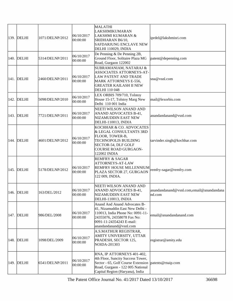
The Patent Office Journal No. 41/2017 Dated 13/10/2017 36698
139. DELHI 1071/DELNP/2012 06/10/2017
00:00:00
MALATHI
LAKSHMIKUMARAN
LAKSHMI KUMARAN &
SRIDHARAN B6/10,
SAFDARJUNG ENCLAVE NEW
DELHI 110029, INDIA
140. DELHI 5314/DELNP/2011 06/10/2017
00:00:00
De Penning & De Penning 2B,
Ground Floor, Solitaire Plaza MG
Road, Gurgaon 122002
141. DELHI 2460/DELNP/2011 06/10/2017
00:00:00
SUBRAMANIAM, NATARAJ &
ASSOCIATES ATTORNEYS-AT-
LAW PATENT AND TRADE
MARK ATTORNEYS E-556,
GREATER KAILASH II NEW
DELHI 110 048
142. DELHI 5098/DELNP/2010 06/10/2017
00:00:00
LEX ORBIS 709/710, Tolstoy
House 15-17, Tolstoy Marg New
Delhi 110 001 India
143. DELHI 7721/DELNP/2011 06/10/2017
00:00:00
NEETI WILSON ANAND AND
ANAND ADVOCATES B-41,
NIZAMUDDIN EAST NEW
DELHI-110013, INDIA
144. DELHI 4601/DELNP/2012 06/10/2017
00:00:00
KOCHHAR & CO. ADVOCATES
& LEGAL CONSULTANTS 3RD
FLOOR, TOWER-B,
TECHNOPOLIS BUILDING
SECTOR-54, DLF GOLF
COURSE ROAD GURGAON-
122002 INDIA
145. DELHI 5178/DELNP/2012 06/10/2017
00:00:00
REMFRY & SAGAR
ATTORNEYS-AT-LAW
REMFRY HOUSE MILLENNIUM
PLAZA SECTOR 27, GURGAON
122 009, INDIA.
146. DELHI 163/DEL/2012 06/10/2017
00:00:00
NEETI WILSON ANAND AND
ANAND ADVOCATES B-41,
NIZAMUDDIN EAST NEW
DELHI-110013, INDIA
[email protected],email@anandandana
nd.com
147. DELHI 986/DEL/2008 06/10/2017
00:00:00
Anand And Anand Advocates B-
41, Nizamuddin East New Delhi -
110013, India Phone No: 0091-11-
24355076, 24358078 Fax No:
0091-11-24354243 E-mail:
148. DELHI 1098/DEL/2009 06/10/2017
00:00:00
A.S.MATHUR REGISTRAR,
AMITY UNIVERSITY, UTTAR
PRADESH, SECTOR 125,
NOIDA-201303
149. DELHI 6541/DELNP/2011 06/10/2017
00:00:00
RNA, IP ATTORNEYS 401-402,
4th Floor, Suncity Success Tower,
Sector - 65, Golf Course Extension
Road, Gurgaon - 122 005 National
Capital Region (Haryana), India
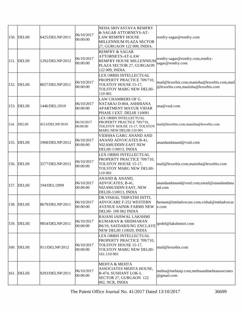
The Patent Office Journal No. 41/2017 Dated 13/10/2017 36699
150. DELHI 6425/DELNP/2011 06/10/2017
00:00:00
NEHA SRIVASTAVA REMFRY
& SAGAR ATTORNEYS-AT-
LAW REMFRY HOUSE
MILLENNIUM PLAZA SECTOR
27, GURGAON 122 009, INDIA.
151. DELHI 1292/DELNP/2012 06/10/2017
00:00:00
REMFRY & SAGAR
ATTORNEYS-AT-LAW
REMFRY HOUSE MILLENNIUM
PLAZA SECTOR 27, GURGAON
122 009, INDIA.
[email protected],remfry-
152. DELHI 8657/DELNP/2011 06/10/2017
00:00:00
LEX ORBIS INTELLECTUAL
PROPERTY PRACTICE 709/710,
TOLSTOY HOUSE 15-17,
TOLSTOY MARG NEW DELHI-
110 001
[email protected],[email protected],mail
@lexorbis.com,[email protected]
153. DELHI 1446/DEL/2010 06/10/2017
00:00:00
LAW CHAMBERS OF G.
NATARAJ D-804, ASHHIANA
APARTMENT MAYUR VIHAR
PHASE I EXT. DELHI 110091
154. DELHI 4513/DELNP/2010 06/10/2017
00:00:00
LEX ORBIS INTELLECTUAL
PROPERTY PRACTICE 709/710,
TOLSTOY HOUSE 15-17, TOLSTOY
MARG NEW DELHI-110 001
[email protected],[email protected]
155. DELHI 1968/DELNP/2012 06/10/2017
00:00:00
VIDISHA GARG ANAND AND
ANAND ADVOCATES B-41,
NIZAMUDDIN EAST NEW
DELHI-110013, INDIA
156. DELHI 3577/DELNP/2012 06/10/2017
00:00:00
LEX ORBIS INTELLECTUAL
PROPERTY PRACTICE 709/710,
TOLSTOY HOUSE 15-17,
TOLSTOY MARG NEW DELHI-
110 001
[email protected],[email protected]
157. DELHI 194/DEL/2009 06/10/2017
00:00:00
ANAND & ANAND,
ADVOCATES, B-41,
NIZAMUDDIN EAST, NEW
DELHI-110013, INDIA
[email protected],email@anandandana
nd.com
158. DELHI 8679/DELNP/2011 06/10/2017
00:00:00
DR.VISHAL TRIPATHI INTTL
ADVOCARE F-252 WESTERN
AVENUE SAINIK FARMS NEW
DELHI- 100 062 INDIA
[email protected],vishal@inttladvocar
e.com
159. DELHI 9854/DELNP/2011 06/10/2017
00:00:00
RAJANI JAISWAL LAKSHMI
KUMARAN & SRIDHARAN
B6/10, SAFDARJUNG ENCLAVE
NEW DELHI 110029, INDIA
160. DELHI 911/DELNP/2012 06/10/2017
00:00:00
LEX ORBIS INTELLECTUAL
PROPERTY PRACTICE 709/710,
TOLSTOY HOUSE 15-17,
TOLSTOY MARG NEW DELHI-
161.110 001
161. DELHI 9293/DELNP/2011 06/10/2017
00:00:00
MEHTA & MEHTA
ASSOCIATES MEHTA HOUSE,
B-474, SUSHANT LOK-I,
SECTOR 27, GURGAON 122
002, NCR, INDIA
[email protected],mehtaandmehtaassociates
@gmail.com
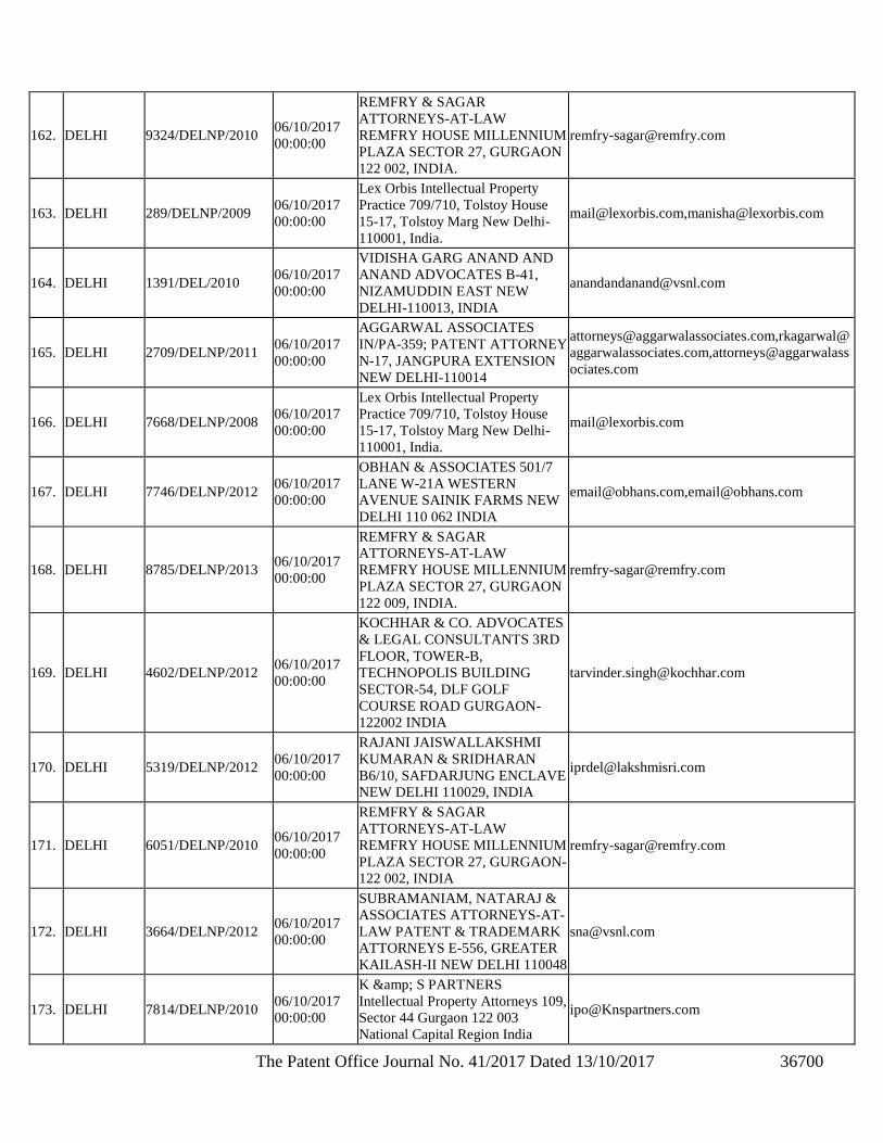
The Patent Office Journal No. 41/2017 Dated 13/10/2017 36700
162. DELHI 9324/DELNP/2010 06/10/2017
00:00:00
REMFRY & SAGAR
ATTORNEYS-AT-LAW
REMFRY HOUSE MILLENNIUM
PLAZA SECTOR 27, GURGAON
122 002, INDIA.
163. DELHI 289/DELNP/2009 06/10/2017
00:00:00
Lex Orbis Intellectual Property
Practice 709/710, Tolstoy House
15-17, Tolstoy Marg New Delhi-
110001, India.
[email protected],[email protected]
164. DELHI 1391/DEL/2010 06/10/2017
00:00:00
VIDISHA GARG ANAND AND
ANAND ADVOCATES B-41,
NIZAMUDDIN EAST NEW
DELHI-110013, INDIA
165. DELHI 2709/DELNP/2011 06/10/2017
00:00:00
AGGARWAL ASSOCIATES
IN/PA-359; PATENT ATTORNEY
N-17, JANGPURA EXTENSION
NEW DELHI-110014
[email protected],rkagarwal@
aggarwalassociates.com,attorneys@aggarwalass
ociates.com
166. DELHI 7668/DELNP/2008 06/10/2017
00:00:00
Lex Orbis Intellectual Property
Practice 709/710, Tolstoy House
15-17, Tolstoy Marg New Delhi-
110001, India.
167. DELHI 7746/DELNP/2012 06/10/2017
00:00:00
OBHAN & ASSOCIATES 501/7
LANE W-21A WESTERN
AVENUE SAINIK FARMS NEW
DELHI 110 062 INDIA
[email protected],[email protected]
168. DELHI 8785/DELNP/2013 06/10/2017
00:00:00
REMFRY & SAGAR
ATTORNEYS-AT-LAW
REMFRY HOUSE MILLENNIUM
PLAZA SECTOR 27, GURGAON
122 009, INDIA.
169. DELHI 4602/DELNP/2012 06/10/2017
00:00:00
KOCHHAR & CO. ADVOCATES
& LEGAL CONSULTANTS 3RD
FLOOR, TOWER-B,
TECHNOPOLIS BUILDING
SECTOR-54, DLF GOLF
COURSE ROAD GURGAON-
122002 INDIA
170. DELHI 5319/DELNP/2012 06/10/2017
00:00:00
RAJANI JAISWALLAKSHMI
KUMARAN & SRIDHARAN
B6/10, SAFDARJUNG ENCLAVE
NEW DELHI 110029, INDIA
171. DELHI 6051/DELNP/2010 06/10/2017
00:00:00
REMFRY & SAGAR
ATTORNEYS-AT-LAW
REMFRY HOUSE MILLENNIUM
PLAZA SECTOR 27, GURGAON-
122 002, INDIA
172. DELHI 3664/DELNP/2012 06/10/2017
00:00:00
SUBRAMANIAM, NATARAJ &
ASSOCIATES ATTORNEYS-AT-
LAW PATENT & TRADEMARK
ATTORNEYS E-556, GREATER
KAILASH-II NEW DELHI 110048
173. DELHI 7814/DELNP/2010 06/10/2017
00:00:00
K & S PARTNERS
Intellectual Property Attorneys 109,
Sector 44 Gurgaon 122 003
National Capital Region India
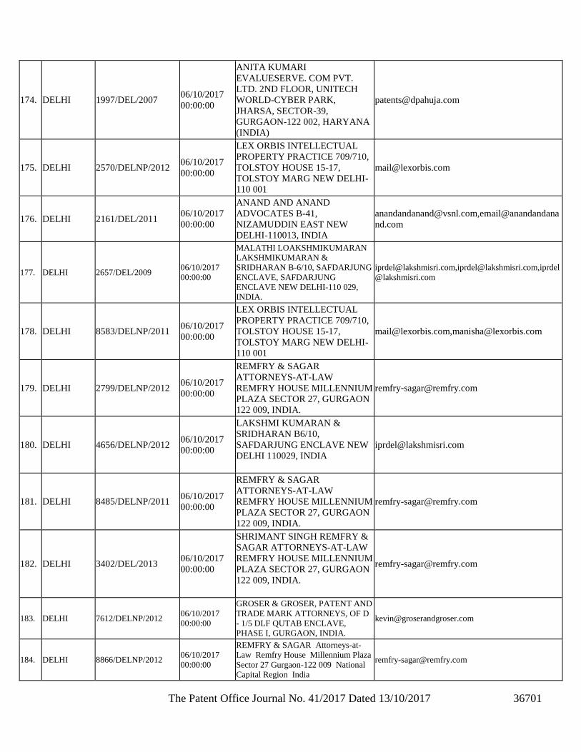
The Patent Office Journal No. 41/2017 Dated 13/10/2017 36701
174. DELHI 1997/DEL/2007 06/10/2017
00:00:00
ANITA KUMARI
EVALUESERVE. COM PVT.
LTD. 2ND FLOOR, UNITECH
WORLD-CYBER PARK,
JHARSA, SECTOR-39,
GURGAON-122 002, HARYANA
(INDIA)
175. DELHI 2570/DELNP/2012 06/10/2017
00:00:00
LEX ORBIS INTELLECTUAL
PROPERTY PRACTICE 709/710,
TOLSTOY HOUSE 15-17,
TOLSTOY MARG NEW DELHI-
110 001
176. DELHI 2161/DEL/2011 06/10/2017
00:00:00
ANAND AND ANAND
ADVOCATES B-41,
NIZAMUDDIN EAST NEW
DELHI-110013, INDIA
[email protected],email@anandandana
nd.com
177. DELHI 2657/DEL/2009 06/10/2017
00:00:00
MALATHI LOAKSHMIKUMARAN
LAKSHMIKUMARAN &
SRIDHARAN B-6/10, SAFDARJUNG
ENCLAVE, SAFDARJUNG
ENCLAVE NEW DELHI-110 029,
INDIA.
[email protected],[email protected],iprdel
@lakshmisri.com
178. DELHI 8583/DELNP/2011 06/10/2017
00:00:00
LEX ORBIS INTELLECTUAL
PROPERTY PRACTICE 709/710,
TOLSTOY HOUSE 15-17,
TOLSTOY MARG NEW DELHI-
110 001
[email protected],[email protected]
179. DELHI 2799/DELNP/2012 06/10/2017
00:00:00
REMFRY & SAGAR
ATTORNEYS-AT-LAW
REMFRY HOUSE MILLENNIUM
PLAZA SECTOR 27, GURGAON
122 009, INDIA.
180. DELHI 4656/DELNP/2012 06/10/2017
00:00:00
LAKSHMI KUMARAN &
SRIDHARAN B6/10,
SAFDARJUNG ENCLAVE NEW
DELHI 110029, INDIA
181. DELHI 8485/DELNP/2011 06/10/2017
00:00:00
REMFRY & SAGAR
ATTORNEYS-AT-LAW
REMFRY HOUSE MILLENNIUM
PLAZA SECTOR 27, GURGAON
122 009, INDIA.
182. DELHI 3402/DEL/2013 06/10/2017
00:00:00
SHRIMANT SINGH REMFRY &
SAGAR ATTORNEYS-AT-LAW
REMFRY HOUSE MILLENNIUM
PLAZA SECTOR 27, GURGAON
122 009, INDIA.
183. DELHI 7612/DELNP/2012 06/10/2017
00:00:00
GROSER & GROSER, PATENT AND
TRADE MARK ATTORNEYS, OF D
- 1/5 DLF QUTAB ENCLAVE,
PHASE I, GURGAON, INDIA.
184. DELHI 8866/DELNP/2012 06/10/2017
00:00:00
REMFRY & SAGAR Attorneys-at-
Law Remfry House Millennium Plaza
Sector 27 Gurgaon-122 009 National
Capital Region India
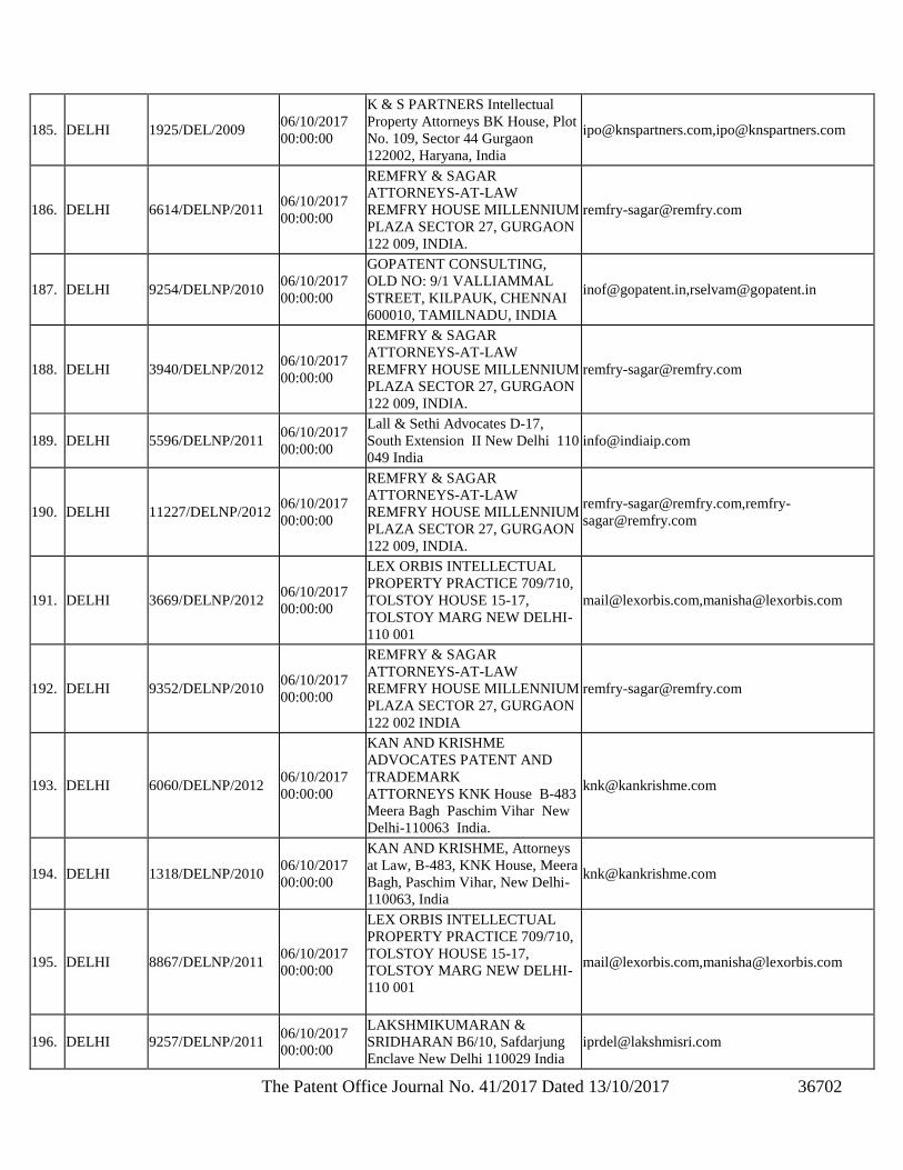
The Patent Office Journal No. 41/2017 Dated 13/10/2017 36702
185. DELHI 1925/DEL/2009 06/10/2017
00:00:00
K & S PARTNERS Intellectual
Property Attorneys BK House, Plot
No. 109, Sector 44 Gurgaon
122002, Haryana, India
[email protected],[email protected]
186. DELHI 6614/DELNP/2011 06/10/2017
00:00:00
REMFRY & SAGAR
ATTORNEYS-AT-LAW
REMFRY HOUSE MILLENNIUM
PLAZA SECTOR 27, GURGAON
122 009, INDIA.
187. DELHI 9254/DELNP/2010 06/10/2017
00:00:00
GOPATENT CONSULTING,
OLD NO: 9/1 VALLIAMMAL
STREET, KILPAUK, CHENNAI
600010, TAMILNADU, INDIA
[email protected],[email protected]
188. DELHI 3940/DELNP/2012 06/10/2017
00:00:00
REMFRY & SAGAR
ATTORNEYS-AT-LAW
REMFRY HOUSE MILLENNIUM
PLAZA SECTOR 27, GURGAON
122 009, INDIA.
189. DELHI 5596/DELNP/2011 06/10/2017
00:00:00
Lall & Sethi Advocates D-17,
South Extension II New Delhi 110
049 India
190. DELHI 11227/DELNP/2012 06/10/2017
00:00:00
REMFRY & SAGAR
ATTORNEYS-AT-LAW
REMFRY HOUSE MILLENNIUM
PLAZA SECTOR 27, GURGAON
122 009, INDIA.
[email protected],remfry-
191. DELHI 3669/DELNP/2012 06/10/2017
00:00:00
LEX ORBIS INTELLECTUAL
PROPERTY PRACTICE 709/710,
TOLSTOY HOUSE 15-17,
TOLSTOY MARG NEW DELHI-
110 001
[email protected],[email protected]
192. DELHI 9352/DELNP/2010 06/10/2017
00:00:00
REMFRY & SAGAR
ATTORNEYS-AT-LAW
REMFRY HOUSE MILLENNIUM
PLAZA SECTOR 27, GURGAON
122 002 INDIA
193. DELHI 6060/DELNP/2012 06/10/2017
00:00:00
KAN AND KRISHME
ADVOCATES PATENT AND
TRADEMARK
ATTORNEYS KNK House B-483
Meera Bagh Paschim Vihar New
Delhi-110063 India.
194. DELHI 1318/DELNP/2010 06/10/2017
00:00:00
KAN AND KRISHME, Attorneys
at Law, B-483, KNK House, Meera
Bagh, Paschim Vihar, New Delhi-
110063, India
195. DELHI 8867/DELNP/2011 06/10/2017
00:00:00
LEX ORBIS INTELLECTUAL
PROPERTY PRACTICE 709/710,
TOLSTOY HOUSE 15-17,
TOLSTOY MARG NEW DELHI-
110 001
[email protected],[email protected]
196. DELHI 9257/DELNP/2011 06/10/2017
00:00:00
LAKSHMIKUMARAN &
SRIDHARAN B6/10, Safdarjung
Enclave New Delhi 110029 India
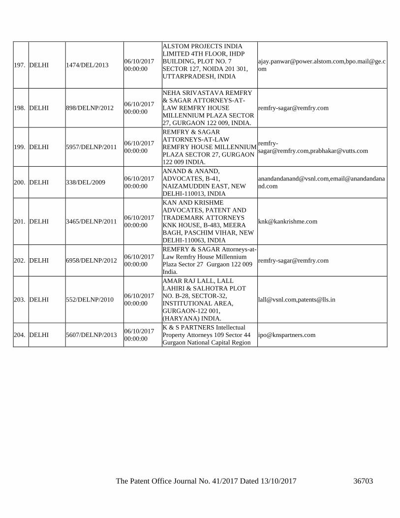
The Patent Office Journal No. 41/2017 Dated 13/10/2017 36703
197. DELHI 1474/DEL/2013 06/10/2017
00:00:00
ALSTOM PROJECTS INDIA
LIMITED 4TH FLOOR, IHDP
BUILDING, PLOT NO. 7
SECTOR 127, NOIDA 201 301,
UTTARPRADESH, INDIA
[email protected],[email protected]
om
198. DELHI 898/DELNP/2012 06/10/2017
00:00:00
NEHA SRIVASTAVA REMFRY
& SAGAR ATTORNEYS-AT-
LAW REMFRY HOUSE
MILLENNIUM PLAZA SECTOR
27, GURGAON 122 009, INDIA.
199. DELHI 5957/DELNP/2011 06/10/2017
00:00:00
REMFRY & SAGAR
ATTORNEYS-AT-LAW
REMFRY HOUSE MILLENNIUM
PLAZA SECTOR 27, GURGAON
122 009 INDIA.
remfry-
[email protected],[email protected]
200. DELHI 338/DEL/2009 06/10/2017
00:00:00
ANAND & ANAND,
ADVOCATES, B-41,
NAIZAMUDDIN EAST, NEW
DELHI-110013, INDIA
[email protected],email@anandandana
nd.com
201. DELHI 3465/DELNP/2011 06/10/2017
00:00:00
KAN AND KRISHME
ADVOCATES, PATENT AND
TRADEMARK ATTORNEYS
KNK HOUSE, B-483, MEERA
BAGH, PASCHIM VIHAR, NEW
DELHI-110063, INDIA
202. DELHI 6958/DELNP/2012 06/10/2017
00:00:00
REMFRY & SAGAR Attorneys-at-
Law Remfry House Millennium
Plaza Sector 27 Gurgaon 122 009
India.
203. DELHI 552/DELNP/2010 06/10/2017
00:00:00
AMAR RAJ LALL, LALL
LAHIRI & SALHOTRA PLOT
NO. B-28, SECTOR-32,
INSTITUTIONAL AREA,
GURGAON-122 001,
(HARYANA) INDIA.
[email protected],[email protected]
204. DELHI 5607/DELNP/2013 06/10/2017
00:00:00
K & S PARTNERS Intellectual
Property Attorneys 109 Sector 44
Gurgaon National Capital Region
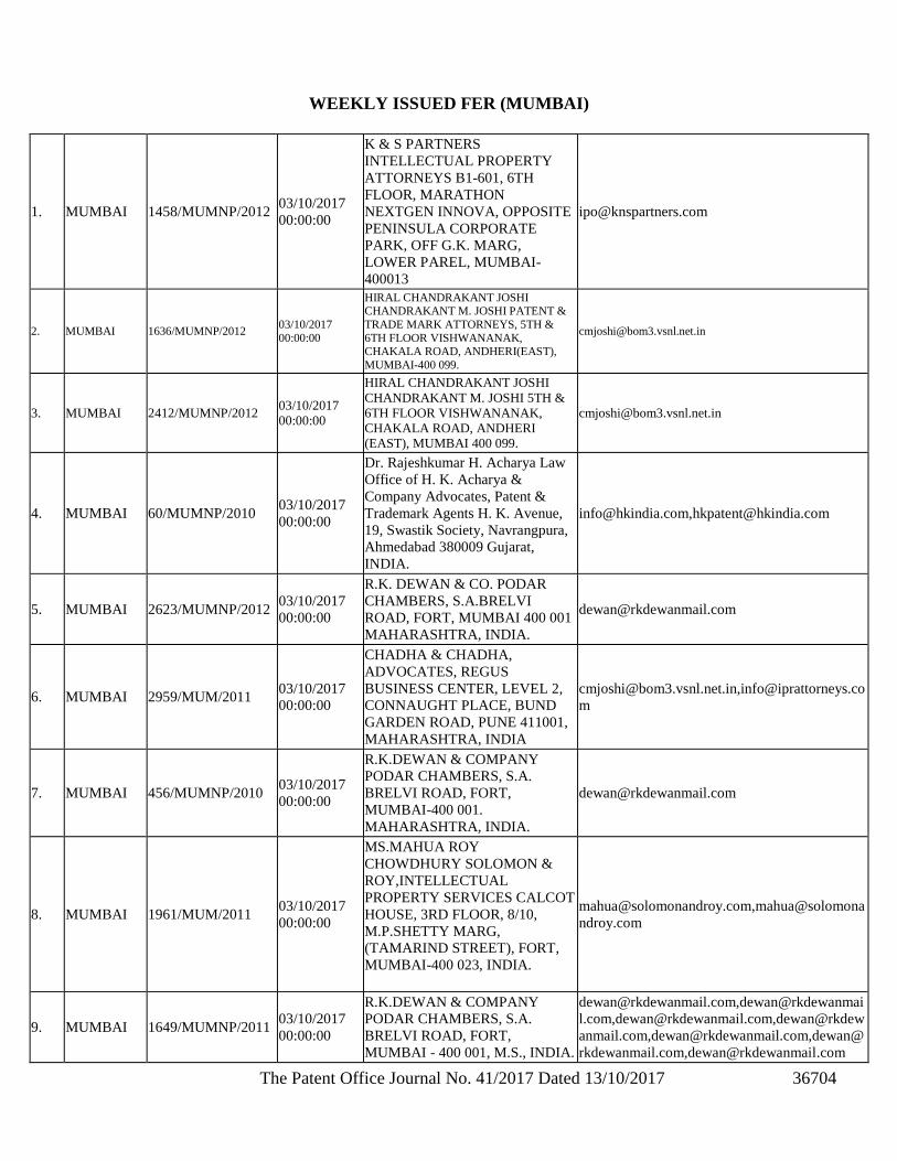
The Patent Office Journal No. 41/2017 Dated 13/10/2017 36704
WEEKLY ISSUED FER (MUMBAI)
1. MUMBAI 1458/MUMNP/2012 03/10/2017
00:00:00
K & S PARTNERS
INTELLECTUAL PROPERTY
ATTORNEYS B1-601, 6TH
FLOOR, MARATHON
NEXTGEN INNOVA, OPPOSITE
PENINSULA CORPORATE
PARK, OFF G.K. MARG,
LOWER PAREL, MUMBAI-
400013
2. MUMBAI 1636/MUMNP/2012 03/10/2017
00:00:00
HIRAL CHANDRAKANT JOSHI CHANDRAKANT M. JOSHI PATENT &
TRADE MARK ATTORNEYS, 5TH &
6TH FLOOR VISHWANANAK, CHAKALA ROAD, ANDHERI(EAST),
MUMBAI-400 099.
3. MUMBAI 2412/MUMNP/2012 03/10/2017
00:00:00
HIRAL CHANDRAKANT JOSHI
CHANDRAKANT M. JOSHI 5TH &
6TH FLOOR VISHWANANAK,
CHAKALA ROAD, ANDHERI
(EAST), MUMBAI 400 099.
4. MUMBAI 60/MUMNP/2010 03/10/2017
00:00:00
Dr. Rajeshkumar H. Acharya Law
Office of H. K. Acharya &
Company Advocates, Patent &
Trademark Agents H. K. Avenue,
19, Swastik Society, Navrangpura,
Ahmedabad 380009 Gujarat,
INDIA.
[email protected],[email protected]
5. MUMBAI 2623/MUMNP/2012 03/10/2017
00:00:00
R.K. DEWAN & CO. PODAR
CHAMBERS, S.A.BRELVI
ROAD, FORT, MUMBAI 400 001
MAHARASHTRA, INDIA.
6. MUMBAI 2959/MUM/2011 03/10/2017
00:00:00
CHADHA & CHADHA,
ADVOCATES, REGUS
BUSINESS CENTER, LEVEL 2,
CONNAUGHT PLACE, BUND
GARDEN ROAD, PUNE 411001,
MAHARASHTRA, INDIA
[email protected],[email protected]
m
7. MUMBAI 456/MUMNP/2010 03/10/2017
00:00:00
R.K.DEWAN & COMPANY
PODAR CHAMBERS, S.A.
BRELVI ROAD, FORT,
MUMBAI-400 001.
MAHARASHTRA, INDIA.
8. MUMBAI 1961/MUM/2011 03/10/2017
00:00:00
MS.MAHUA ROY
CHOWDHURY SOLOMON &
ROY,INTELLECTUAL
PROPERTY SERVICES CALCOT
HOUSE, 3RD FLOOR, 8/10,
M.P.SHETTY MARG,
(TAMARIND STREET), FORT,
MUMBAI-400 023, INDIA.
[email protected],mahua@solomona
ndroy.com
9. MUMBAI 1649/MUMNP/2011 03/10/2017
00:00:00
R.K.DEWAN & COMPANY
PODAR CHAMBERS, S.A.
BRELVI ROAD, FORT,
MUMBAI - 400 001, M.S., INDIA.
[email protected],dewan@rkdewanmai
l.com,[email protected],dewan@rkdew
anmail.com,[email protected],dewan@
rkdewanmail.com,[email protected]
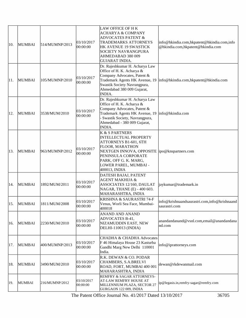
The Patent Office Journal No. 41/2017 Dated 13/10/2017 36705
10. MUMBAI 514/MUMNP/2013 03/10/2017
00:00:00
LAW OFFICE OF H K
ACHARYA & COMPANY
ADVOCATES PATENT &
TRADEMARKS ATTORNEYS
HK AVENUE 19 SWASTICK
SOCIETY NAVRANGPURA
AHMEDABAD 380 009
GUJARAT INDIA.
[email protected],[email protected],info
@hkindia.com,[email protected]
11. MUMBAI 105/MUMNP/2010 03/10/2017
00:00:00
Dr. Rajeshkumar H. Acharya Law
Office of H. K. Acharya &
Company Advocates, Patent &
Trademark Agents HK Avenue, 19
Swastik Society Navrangpura,
Ahmedabad 380 009 Gujarat,
INDIA.
[email protected],[email protected]
12. MUMBAI 3538/MUM/2010 03/10/2017
00:00:00
Dr. Rajeshkumar H. Acharya Law
Office of H. K. Acharya &
Company Advocates, Patent &
Trademark Agents HK Avenue, 19
- Swastik Society, Navrangpura,
Ahmedabad - 380 009 Gujarat,
INDIA.
13. MUMBAI 963/MUMNP/2012 03/10/2017
00:00:00
K & S PARTNERS
INTELLECTUAL PROPERTY
ATTORNEYS B1-601, 6TH
FLOOR, MARATHON
NEXTGEN INNOVA, OPPOSITE
PENINSULA CORPORATE
PARK, OFF G. K. MARG,
LOWER PAREL, MUMBAI -
400013, INDIA
14. MUMBAI 1892/MUM/2011 03/10/2017
00:00:00
DATESH BAJAJ, PATENT
AGENT MAKHIJA &
ASSOCIATES 12/160, DAULAT
NAGAR, THANE (E) - 400 603.
MAHARASHTRA, INDIA
15. MUMBAI 1811/MUM/2008 03/10/2017
00:00:00
KRISHNA & SAURASTRI 74-F
Venus, Worli Sea Face, Mumbai-
400018
[email protected],info@krishnaand
saurastri.com
16. MUMBAI 2230/MUM/2010 03/10/2017
00:00:00
ANAND AND ANAND
ADVOCATES B-41,
NIZAMUDDIN EAST, NEW
DELHI-110013 (INDIA)
[email protected],email@anandandana
nd.com
17. MUMBAI 400/MUMNP/2013 03/10/2017
00:00:00
CHADHA & CHADHA Advocates
F 46 Himalaya House 23 Kasturba
Gandhi Marg New Delhi 110001
India.
18. MUMBAI 3490/MUM/2010 03/10/2017
00:00:00
R.K. DEWAN & CO. PODAR
CHAMBERS, S.A.BRELVI
ROAD, FORT, MUMBAI 400 001
MAHARASHTRA, INDIA
19. MUMBAI 216/MUMNP/2012 03/10/2017
00:00:00
REMFRY & SAGAR ATTORNEYS-
AT-LAW REMFRY HOUSE AT
MILLENNIUM PLAZA, SECTOR 27
GURGAON 122 009, INDIA
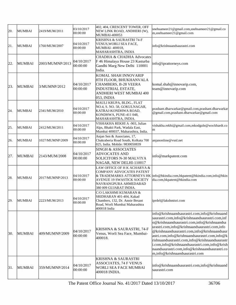
The Patent Office Journal No. 41/2017 Dated 13/10/2017 36706
20. MUMBAI 2419/MUM/2011 03/10/2017
00:00:00
402, 404, CRESCENT TOWER, OFF
NEW LINK ROAD, ANDHERI (W),
MUMBAI-400053
[email protected],[email protected]
21. MUMBAI 1760/MUM/2007 04/10/2017
00:00:00
KRISHNA & SAURASTRI 74-F
VENUS,WORLI SEA FACE,
MUMBAI- 400018,
MAHARASHTRA, INDIA
22. MUMBAI 2003/MUMNP/2013 04/10/2017
00:00:00
CHADHA & CHADHA Advocates
F 46 Himalaya House 23 Kasturba
Gandhi Marg New Delhi 110001
India.
23. MUMBAI 3/MUMNP/2012 04/10/2017
00:00:00
KOMAL SHAH INNOVARIP
8TH FLOOR, BHUKHANVALA
CHAMBERS, B-28 VEERA
INDUSTRIAL ESTATE,
ANDHERI WEST MUMBAI 400
053, INDIA
24. MUMBAI 2341/MUM/2010 04/10/2017
00:00:00
MAULI KRUPA, BLDG., FLAT
NO.4, S. NO. 58, GOKULNAGAR,
KATRAJ-KONDHWA ROAD,
KONDHWA, PUNE-411 048,
MAHARASHTRA, INDIA.
[email protected],prashant.dharwarkar
@gmail.com,[email protected]
25. MUMBAI 2412/MUM/2011 04/10/2017
00:00:00
VISHAKHA REKHI A -903, Julian
Alps, Bhakti Park, Wadala East,
Mumbai 400037, Maharashtra, India.
[email protected],[email protected]
m
26. MUMBAI 1027/MUMNP/2009 04/10/2017
00:00:00
Anjan Sen & Associates, 17,
Chakraberia Road South, Kolkata 700
025, India. Mobile: 9830050839
27. MUMBAI 2143/MUM/2008 04/10/2017
00:00:00
SINGH & ASSOCIATES
ADVOCATES AND
SOLICITORS N-30 MALVIYA
NAGAR, NEW DELHI-110017
28. MUMBAI 2017/MUMNP/2013 04/10/2017
00:00:00
LAW OFFICE OF H K ACHARYA &
COMPANY ADVOCATES PATENT
& TRADEMARKS ATTORNEYS HK
AVENUE 19 SWASTICK SOCIETY
NAVRANGPURA AHMEDABAD
380 009 GUJARAT INDIA.
[email protected],[email protected],info@hkin
dia.com,[email protected]
29. MUMBAI 2223/MUM/2013 04/10/2017
00:00:00
C/O LAKSHMI KUMARAN &
SRIDHARAN 401-404, Kakad
Chambers, 132, Dr. Annie Besant
Road, Worli Mumbai Maharashtra
400018 India
30. MUMBAI 409/MUMNP/2009 04/10/2017
00:00:00
KRISHNA & SAURASTRI, 74-F
Venus, Worli Sea Face, Mumbai-
400018.
[email protected],info@krishnaand
saurastri.com,[email protected],inf
[email protected],info@krishnaandsa
urastri.com,[email protected],info
@krishnaandsaurastri.com,info@krishnaandsaur
astri.com,[email protected],info@k
rishnaandsaurastri.com,info@krishnaandsaurastr
i.com,[email protected],info@krish
naandsaurastri.com,[email protected]
31. MUMBAI 359/MUMNP/2014 04/10/2017
00:00:00
KRISHNA & SAURASTRI
ASSOCIATES, 74 F VENUS
WORLI SEA FACE MUMBAI
400018 INDIA.
[email protected],info@krishnaand
saurastri.com
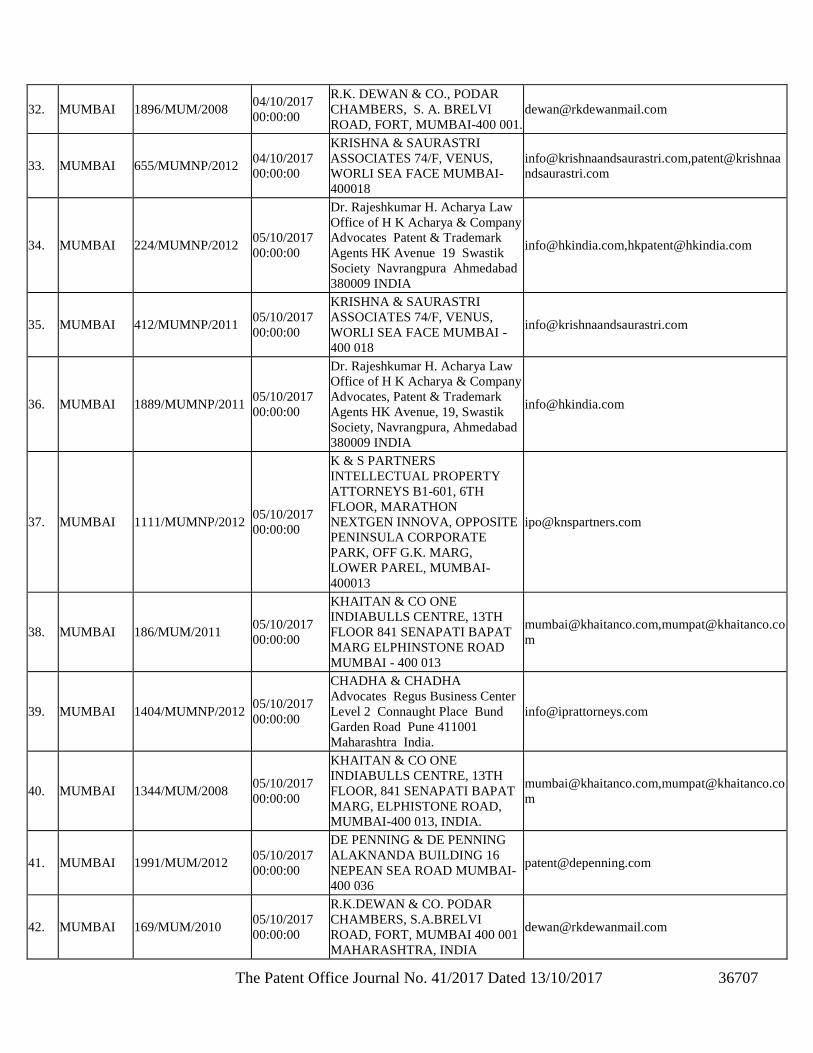
The Patent Office Journal No. 41/2017 Dated 13/10/2017 36707
32. MUMBAI 1896/MUM/2008 04/10/2017
00:00:00
R.K. DEWAN & CO., PODAR
CHAMBERS, S. A. BRELVI
ROAD, FORT, MUMBAI-400 001.
33. MUMBAI 655/MUMNP/2012 04/10/2017
00:00:00
KRISHNA & SAURASTRI
ASSOCIATES 74/F, VENUS,
WORLI SEA FACE MUMBAI-
400018
[email protected],patent@krishnaa
ndsaurastri.com
34. MUMBAI 224/MUMNP/2012 05/10/2017
00:00:00
Dr. Rajeshkumar H. Acharya Law
Office of H K Acharya & Company
Advocates Patent & Trademark
Agents HK Avenue 19 Swastik
Society Navrangpura Ahmedabad
380009 INDIA
[email protected],[email protected]
35. MUMBAI 412/MUMNP/2011 05/10/2017
00:00:00
KRISHNA & SAURASTRI
ASSOCIATES 74/F, VENUS,
WORLI SEA FACE MUMBAI -
400 018
36. MUMBAI 1889/MUMNP/2011 05/10/2017
00:00:00
Dr. Rajeshkumar H. Acharya Law
Office of H K Acharya & Company
Advocates, Patent & Trademark
Agents HK Avenue, 19, Swastik
Society, Navrangpura, Ahmedabad
380009 INDIA
37. MUMBAI 1111/MUMNP/2012 05/10/2017
00:00:00
K & S PARTNERS
INTELLECTUAL PROPERTY
ATTORNEYS B1-601, 6TH
FLOOR, MARATHON
NEXTGEN INNOVA, OPPOSITE
PENINSULA CORPORATE
PARK, OFF G.K. MARG,
LOWER PAREL, MUMBAI-
400013
38. MUMBAI 186/MUM/2011 05/10/2017
00:00:00
KHAITAN & CO ONE
INDIABULLS CENTRE, 13TH
FLOOR 841 SENAPATI BAPAT
MARG ELPHINSTONE ROAD
MUMBAI - 400 013
[email protected],[email protected]
m
39. MUMBAI 1404/MUMNP/2012 05/10/2017
00:00:00
CHADHA & CHADHA
Advocates Regus Business Center
Level 2 Connaught Place Bund
Garden Road Pune 411001
Maharashtra India.
40. MUMBAI 1344/MUM/2008 05/10/2017
00:00:00
KHAITAN & CO ONE
INDIABULLS CENTRE, 13TH
FLOOR, 841 SENAPATI BAPAT
MARG, ELPHISTONE ROAD,
MUMBAI-400 013, INDIA.
[email protected],[email protected]
m
41. MUMBAI 1991/MUM/2012 05/10/2017
00:00:00
DE PENNING & DE PENNING
ALAKNANDA BUILDING 16
NEPEAN SEA ROAD MUMBAI-
400 036
42. MUMBAI 169/MUM/2010 05/10/2017
00:00:00
R.K.DEWAN & CO. PODAR
CHAMBERS, S.A.BRELVI
ROAD, FORT, MUMBAI 400 001
MAHARASHTRA, INDIA
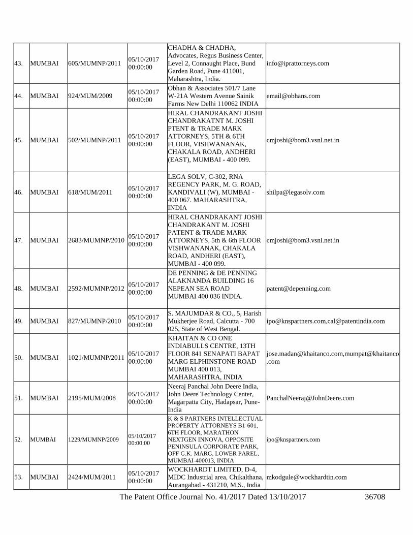
The Patent Office Journal No. 41/2017 Dated 13/10/2017 36708
43. MUMBAI 605/MUMNP/2011 05/10/2017
00:00:00
CHADHA & CHADHA,
Advocates, Regus Business Center,
Level 2, Connaught Place, Bund
Garden Road, Pune 411001,
Maharashtra, India.
44. MUMBAI 924/MUM/2009 05/10/2017
00:00:00
Obhan & Associates 501/7 Lane
W-21A Western Avenue Sainik
Farms New Delhi 110062 INDIA
45. MUMBAI 502/MUMNP/2011 05/10/2017
00:00:00
HIRAL CHANDRAKANT JOSHI
CHANDRAKATNT M. JOSHI
PTENT & TRADE MARK
ATTORNEYS, 5TH & 6TH
FLOOR, VISHWANANAK,
CHAKALA ROAD, ANDHERI
(EAST), MUMBAI - 400 099.
46. MUMBAI 618/MUM/2011 05/10/2017
00:00:00
LEGA SOLV, C-302, RNA
REGENCY PARK, M. G. ROAD,
KANDIVALI (W), MUMBAI -
400 067. MAHARASHTRA,
INDIA
47. MUMBAI 2683/MUMNP/2010 05/10/2017
00:00:00
HIRAL CHANDRAKANT JOSHI
CHANDRAKANT M. JOSHI
PATENT & TRADE MARK
ATTORNEYS, 5th & 6th FLOOR
VISHWANANAK, CHAKALA
ROAD, ANDHERI (EAST),
MUMBAI - 400 099.
48. MUMBAI 2592/MUMNP/2012 05/10/2017
00:00:00
DE PENNING & DE PENNING
ALAKNANDA BUILDING 16
NEPEAN SEA ROAD
MUMBAI 400 036 INDIA.
49. MUMBAI 827/MUMNP/2010 05/10/2017
00:00:00
S. MAJUMDAR & CO., 5, Harish
Mukherjee Road, Calcutta - 700
025, State of West Bengal.
[email protected],[email protected]
50. MUMBAI 1021/MUMNP/2011 05/10/2017
00:00:00
KHAITAN & CO ONE
INDIABULLS CENTRE, 13TH
FLOOR 841 SENAPATI BAPAT
MARG ELPHINSTONE ROAD
MUMBAI 400 013,
MAHARASHTRA, INDIA
[email protected],mumpat@khaitanco
.com
51. MUMBAI 2195/MUM/2008 05/10/2017
00:00:00
Neeraj Panchal John Deere India,
John Deere Technology Center,
Magarpatta City, Hadapsar, Pune-
India
52. MUMBAI 1229/MUMNP/2009 05/10/2017
00:00:00
K & S PARTNERS INTELLECTUAL
PROPERTY ATTORNEYS B1-601,
6TH FLOOR, MARATHON
NEXTGEN INNOVA, OPPOSITE
PENINSULA CORPORATE PARK,
OFF G.K. MARG, LOWER PAREL,
MUMBAI-400013, INDIA
53. MUMBAI 2424/MUM/2011 05/10/2017
00:00:00
WOCKHARDT LIMITED, D-4,
MIDC Industrial area, Chikalthana,
Aurangabad - 431210, M.S., India
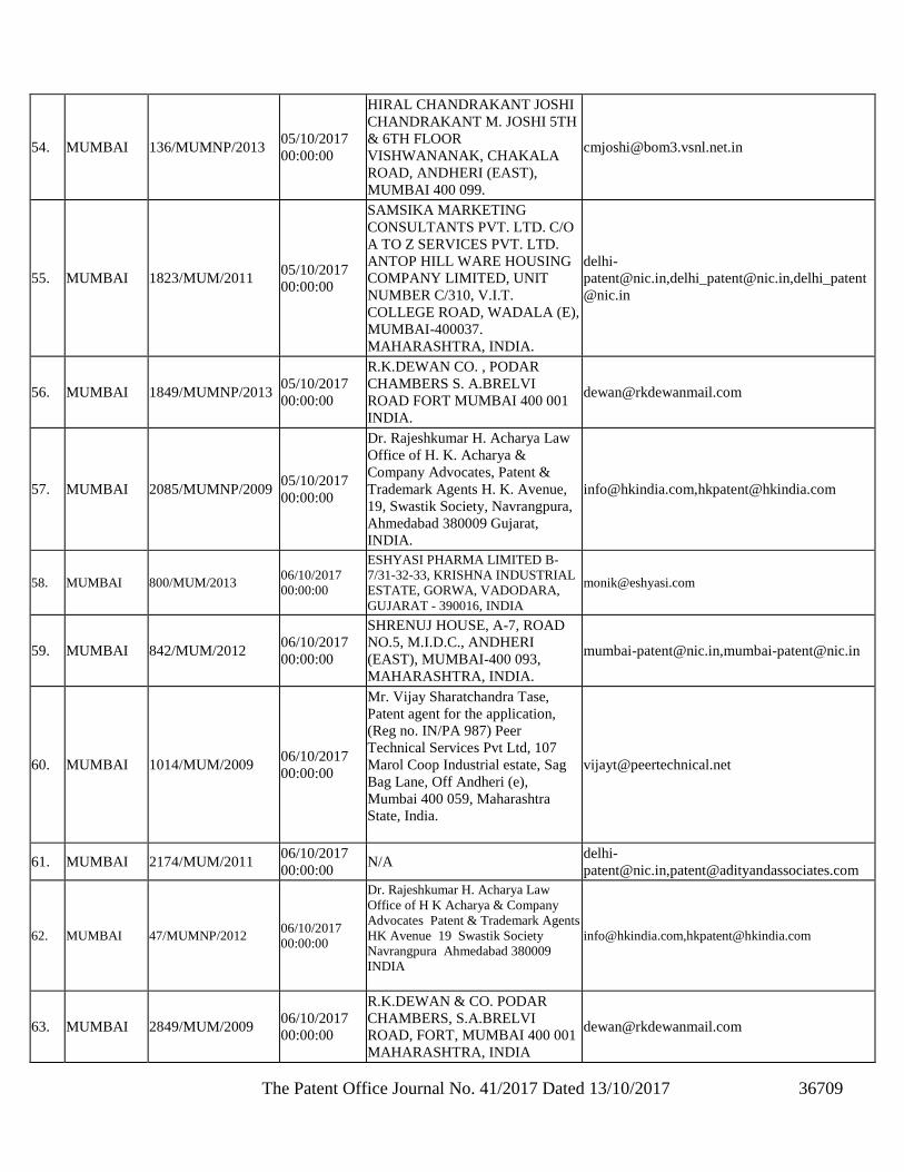
The Patent Office Journal No. 41/2017 Dated 13/10/2017 36709
54. MUMBAI 136/MUMNP/2013 05/10/2017
00:00:00
HIRAL CHANDRAKANT JOSHI
CHANDRAKANT M. JOSHI 5TH
& 6TH FLOOR
VISHWANANAK, CHAKALA
ROAD, ANDHERI (EAST),
MUMBAI 400 099.
55. MUMBAI 1823/MUM/2011 05/10/2017
00:00:00
SAMSIKA MARKETING
CONSULTANTS PVT. LTD. C/O
A TO Z SERVICES PVT. LTD.
ANTOP HILL WARE HOUSING
COMPANY LIMITED, UNIT
NUMBER C/310, V.I.T.
COLLEGE ROAD, WADALA (E),
MUMBAI-400037.
MAHARASHTRA, INDIA.
delhi-
[email protected],[email protected],delhi_patent
@nic.in
56. MUMBAI 1849/MUMNP/2013 05/10/2017
00:00:00
R.K.DEWAN CO. , PODAR
CHAMBERS S. A.BRELVI
ROAD FORT MUMBAI 400 001
INDIA.
57. MUMBAI 2085/MUMNP/2009 05/10/2017
00:00:00
Dr. Rajeshkumar H. Acharya Law
Office of H. K. Acharya &
Company Advocates, Patent &
Trademark Agents H. K. Avenue,
19, Swastik Society, Navrangpura,
Ahmedabad 380009 Gujarat,
INDIA.
[email protected],[email protected]
58. MUMBAI 800/MUM/2013 06/10/2017
00:00:00
ESHYASI PHARMA LIMITED B-
7/31-32-33, KRISHNA INDUSTRIAL
ESTATE, GORWA, VADODARA,
GUJARAT - 390016, INDIA
59. MUMBAI 842/MUM/2012 06/10/2017
00:00:00
SHRENUJ HOUSE, A-7, ROAD
NO.5, M.I.D.C., ANDHERI
(EAST), MUMBAI-400 093,
MAHARASHTRA, INDIA.
[email protected],[email protected]
60. MUMBAI 1014/MUM/2009 06/10/2017
00:00:00
Mr. Vijay Sharatchandra Tase,
Patent agent for the application,
(Reg no. IN/PA 987) Peer
Technical Services Pvt Ltd, 107
Marol Coop Industrial estate, Sag
Bag Lane, Off Andheri (e),
Mumbai 400 059, Maharashtra
State, India.
61. MUMBAI 2174/MUM/2011 06/10/2017
00:00:00 N/A
delhi-
[email protected],[email protected]
62. MUMBAI 47/MUMNP/2012 06/10/2017
00:00:00
Dr. Rajeshkumar H. Acharya Law
Office of H K Acharya & Company
Advocates Patent & Trademark Agents
HK Avenue 19 Swastik Society
Navrangpura Ahmedabad 380009
INDIA
[email protected],[email protected]
63. MUMBAI 2849/MUM/2009 06/10/2017
00:00:00
R.K.DEWAN & CO. PODAR
CHAMBERS, S.A.BRELVI
ROAD, FORT, MUMBAI 400 001
MAHARASHTRA, INDIA
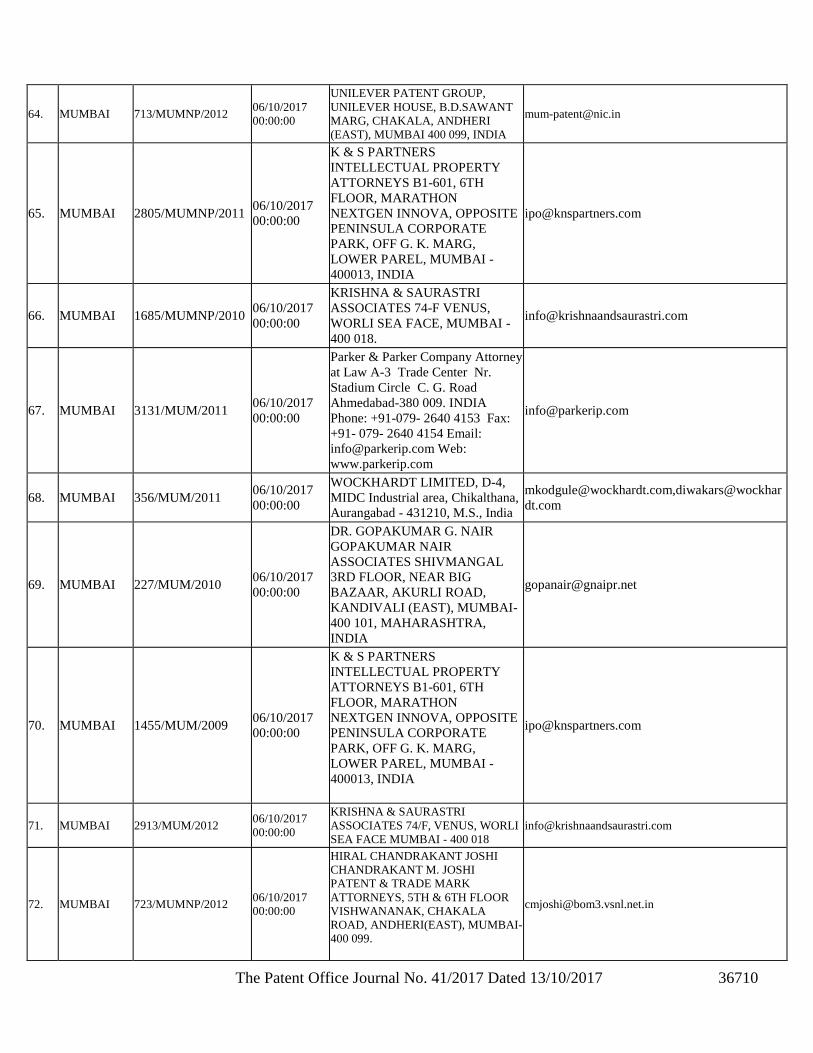
The Patent Office Journal No. 41/2017 Dated 13/10/2017 36710
64. MUMBAI 713/MUMNP/2012 06/10/2017
00:00:00
UNILEVER PATENT GROUP,
UNILEVER HOUSE, B.D.SAWANT
MARG, CHAKALA, ANDHERI
(EAST), MUMBAI 400 099, INDIA
65. MUMBAI 2805/MUMNP/2011 06/10/2017
00:00:00
K & S PARTNERS
INTELLECTUAL PROPERTY
ATTORNEYS B1-601, 6TH
FLOOR, MARATHON
NEXTGEN INNOVA, OPPOSITE
PENINSULA CORPORATE
PARK, OFF G. K. MARG,
LOWER PAREL, MUMBAI -
400013, INDIA
66. MUMBAI 1685/MUMNP/2010 06/10/2017
00:00:00
KRISHNA & SAURASTRI
ASSOCIATES 74-F VENUS,
WORLI SEA FACE, MUMBAI -
400 018.
67. MUMBAI 3131/MUM/2011 06/10/2017
00:00:00
Parker & Parker Company Attorney
at Law A-3 Trade Center Nr.
Stadium Circle C. G. Road
Ahmedabad-380 009. INDIA
Phone: +91-079- 2640 4153 Fax:
+91- 079- 2640 4154 Email:
[email protected] Web:
www.parkerip.com
68. MUMBAI 356/MUM/2011 06/10/2017
00:00:00
WOCKHARDT LIMITED, D-4,
MIDC Industrial area, Chikalthana,
Aurangabad - 431210, M.S., India
[email protected],diwakars@wockhar
dt.com
69. MUMBAI 227/MUM/2010 06/10/2017
00:00:00
DR. GOPAKUMAR G. NAIR
GOPAKUMAR NAIR
ASSOCIATES SHIVMANGAL
3RD FLOOR, NEAR BIG
BAZAAR, AKURLI ROAD,
KANDIVALI (EAST), MUMBAI-
400 101, MAHARASHTRA,
INDIA
70. MUMBAI 1455/MUM/2009 06/10/2017
00:00:00
K & S PARTNERS
INTELLECTUAL PROPERTY
ATTORNEYS B1-601, 6TH
FLOOR, MARATHON
NEXTGEN INNOVA, OPPOSITE
PENINSULA CORPORATE
PARK, OFF G. K. MARG,
LOWER PAREL, MUMBAI -
400013, INDIA
71. MUMBAI 2913/MUM/2012 06/10/2017
00:00:00
KRISHNA & SAURASTRI
ASSOCIATES 74/F, VENUS, WORLI
SEA FACE MUMBAI - 400 018
72. MUMBAI 723/MUMNP/2012 06/10/2017
00:00:00
HIRAL CHANDRAKANT JOSHI
CHANDRAKANT M. JOSHI
PATENT & TRADE MARK
ATTORNEYS, 5TH & 6TH FLOOR
VISHWANANAK, CHAKALA
ROAD, ANDHERI(EAST), MUMBAI-
400 099.
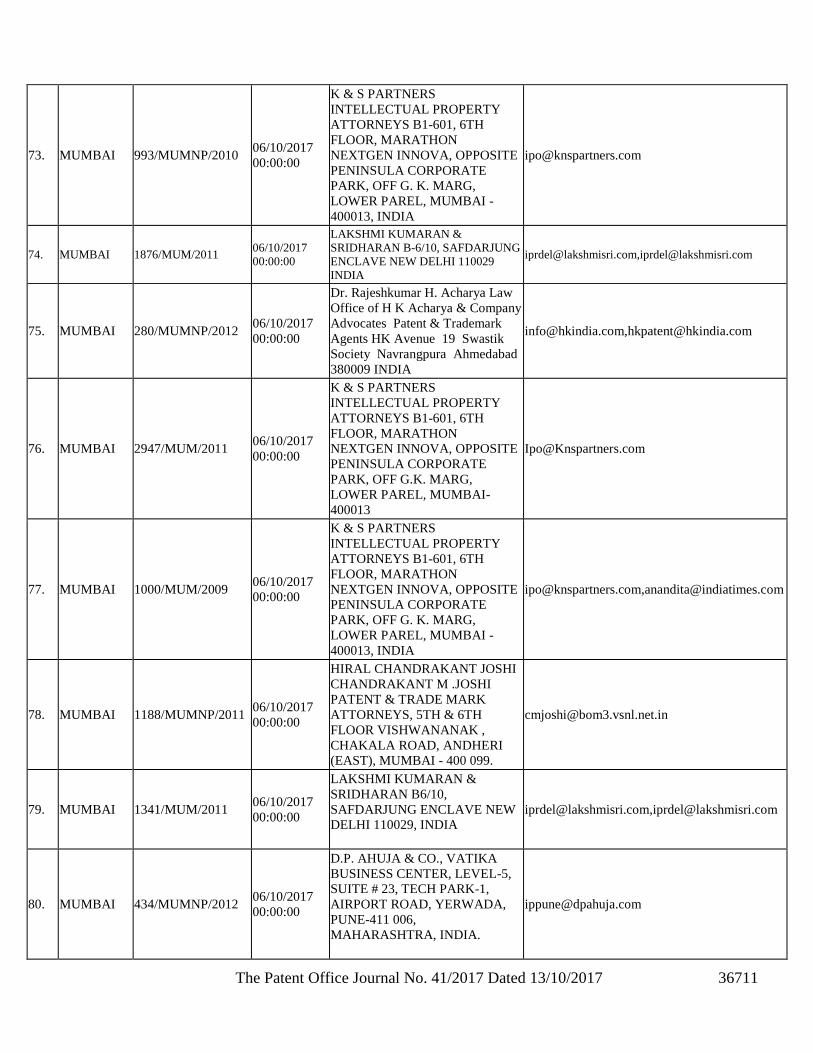
The Patent Office Journal No. 41/2017 Dated 13/10/2017 36711
73. MUMBAI 993/MUMNP/2010 06/10/2017
00:00:00
K & S PARTNERS
INTELLECTUAL PROPERTY
ATTORNEYS B1-601, 6TH
FLOOR, MARATHON
NEXTGEN INNOVA, OPPOSITE
PENINSULA CORPORATE
PARK, OFF G. K. MARG,
LOWER PAREL, MUMBAI -
400013, INDIA
74. MUMBAI 1876/MUM/2011 06/10/2017
00:00:00
LAKSHMI KUMARAN &
SRIDHARAN B-6/10, SAFDARJUNG
ENCLAVE NEW DELHI 110029
INDIA
[email protected],[email protected]
75. MUMBAI 280/MUMNP/2012 06/10/2017
00:00:00
Dr. Rajeshkumar H. Acharya Law
Office of H K Acharya & Company
Advocates Patent & Trademark
Agents HK Avenue 19 Swastik
Society Navrangpura Ahmedabad
380009 INDIA
[email protected],[email protected]
76. MUMBAI 2947/MUM/2011 06/10/2017
00:00:00
K & S PARTNERS
INTELLECTUAL PROPERTY
ATTORNEYS B1-601, 6TH
FLOOR, MARATHON
NEXTGEN INNOVA, OPPOSITE
PENINSULA CORPORATE
PARK, OFF G.K. MARG,
LOWER PAREL, MUMBAI-
400013
77. MUMBAI 1000/MUM/2009 06/10/2017
00:00:00
K & S PARTNERS
INTELLECTUAL PROPERTY
ATTORNEYS B1-601, 6TH
FLOOR, MARATHON
NEXTGEN INNOVA, OPPOSITE
PENINSULA CORPORATE
PARK, OFF G. K. MARG,
LOWER PAREL, MUMBAI -
400013, INDIA
[email protected],[email protected]
78. MUMBAI 1188/MUMNP/2011 06/10/2017
00:00:00
HIRAL CHANDRAKANT JOSHI
CHANDRAKANT M .JOSHI
PATENT & TRADE MARK
ATTORNEYS, 5TH & 6TH
FLOOR VISHWANANAK ,
CHAKALA ROAD, ANDHERI
(EAST), MUMBAI - 400 099.
79. MUMBAI 1341/MUM/2011 06/10/2017
00:00:00
LAKSHMI KUMARAN &
SRIDHARAN B6/10,
SAFDARJUNG ENCLAVE NEW
DELHI 110029, INDIA
[email protected],[email protected]
80. MUMBAI 434/MUMNP/2012 06/10/2017
00:00:00
D.P. AHUJA & CO., VATIKA
BUSINESS CENTER, LEVEL-5,
SUITE # 23, TECH PARK-1,
AIRPORT ROAD, YERWADA,
PUNE-411 006,
MAHARASHTRA, INDIA.
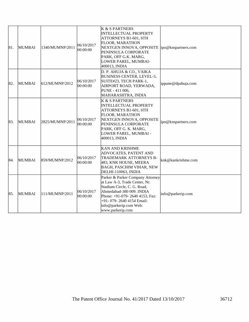
The Patent Office Journal No. 41/2017 Dated 13/10/2017 36712
81. MUMBAI 1340/MUMNP/2011 06/10/2017
00:00:00
K & S PARTNERS
INTELLECTUAL PROPERTY
ATTORNEYS B1-601, 6TH
FLOOR, MARATHON
NEXTGEN INNOVA, OPPOSITE
PENINSULA CORPORATE
PARK, OFF G.K. MARG,
LOWER PAREL, MUMBAI-
400013, INDIA
82. MUMBAI 612/MUMNP/2012 06/10/2017
00:00:00
D. P. AHUJA & CO., VAIKA
BUSINESS CENTER, LEVEL-5,
SUITE#23, TECH PARK-1,
AIRPORT ROAD, YERWADA,
PUNE - 411 006,
MAHARASHTRA, INDIA
83. MUMBAI 2825/MUMNP/2011 06/10/2017
00:00:00
K & S PARTNERS
INTELLECTUAL PROPERTY
ATTORNEYS B1-601, 6TH
FLOOR, MARATHON
NEXTGEN INNOVA, OPPOSITE
PENINSULA CORPORATE
PARK, OFF G. K. MARG,
LOWER PAREL, MUMBAI -
400013, INDIA
84. MUMBAI 859/MUMNP/2012 06/10/2017
00:00:00
KAN AND KRISHME
ADVOCATES, PATENT AND
TRADEMARK ATTORNEYS B-
483, KNK HOUSE, MEERA
BAGH, PASCHIM VIHAR, NEW
DELHI-110063, INDIA
85. MUMBAI 111/MUMNP/2011 06/10/2017
00:00:00
Parker & Parker Company Attorney
at Law A-3, Trade Center, Nr.
Stadium Circle, C. G. Road,
Ahmedabad-380 009. INDIA
Phone: +91-079- 2640 4153, Fax:
+91- 079- 2640 4154 Email:
[email protected] Web:
www.parkerip.com
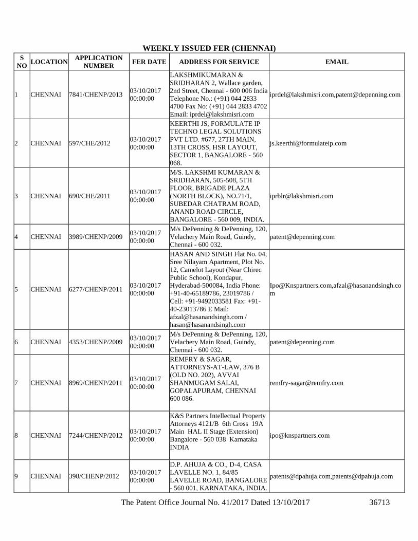
The Patent Office Journal No. 41/2017 Dated 13/10/2017 36713
WEEKLY ISSUED FER (CHENNAI)
S
NO LOCATION
APPLICATION
NUMBER FER DATE ADDRESS FOR SERVICE EMAIL
1 CHENNAI 7841/CHENP/2013 03/10/2017
00:00:00
LAKSHMIKUMARAN &
SRIDHARAN 2, Wallace garden,
2nd Street, Chennai - 600 006 India
Telephone No.: (+91) 044 2833
4700 Fax No: (+91) 044 2833 4702
Email: [email protected]
[email protected],[email protected]
2 CHENNAI 597/CHE/2012 03/10/2017
00:00:00
KEERTHI JS, FORMULATE IP
TECHNO LEGAL SOLUTIONS
PVT LTD. #677, 27TH MAIN,
13TH CROSS, HSR LAYOUT,
SECTOR 1, BANGALORE - 560
068.
3 CHENNAI 690/CHE/2011 03/10/2017
00:00:00
M/S. LAKSHMI KUMARAN &
SRIDHARAN, 505-508, 5TH
FLOOR, BRIGADE PLAZA
(NORTH BLOCK), NO.71/1,
SUBEDAR CHATRAM ROAD,
ANAND ROAD CIRCLE,
BANGALORE - 560 009, INDIA.
4 CHENNAI 3989/CHENP/2009 03/10/2017
00:00:00
M/s DePenning & DePenning, 120,
Velachery Main Road, Guindy,
Chennai - 600 032.
5 CHENNAI 6277/CHENP/2011 03/10/2017
00:00:00
HASAN AND SINGH Flat No. 04,
Sree Nilayam Apartment, Plot No.
12, Camelot Layout (Near Chirec
Public School), Kondapur,
Hyderabad-500084, India Phone:
+91-40-65189786, 23019786 /
Cell: +91-9492033581 Fax: +91-
40-23013786 E Mail:
[email protected],[email protected]
m
6 CHENNAI 4353/CHENP/2009 03/10/2017
00:00:00
M/s DePenning & DePenning, 120,
Velachery Main Road, Guindy,
Chennai - 600 032.
7 CHENNAI 8969/CHENP/2011 03/10/2017
00:00:00
REMFRY & SAGAR,
ATTORNEYS-AT-LAW, 376 B
(OLD NO. 202), AVVAI
SHANMUGAM SALAI,
GOPALAPURAM, CHENNAI
600 086.
8 CHENNAI 7244/CHENP/2012 03/10/2017
00:00:00
K&S Partners Intellectual Property
Attorneys 4121/B 6th Cross 19A
Main HAL II Stage (Extension)
Bangalore - 560 038 Karnataka
INDIA
9 CHENNAI 398/CHENP/2012 03/10/2017
00:00:00
D.P. AHUJA & CO., D-4, CASA
LAVELLE NO. 1, 84/85
LAVELLE ROAD, BANGALORE
- 560 001, KARNATAKA, INDIA.
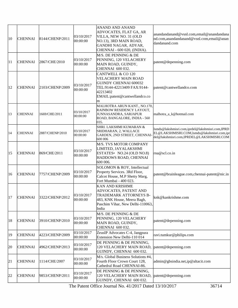
The Patent Office Journal No. 41/2017 Dated 13/10/2017 36714
10 CHENNAI 8144/CHENP/2011 03/10/2017
00:00:00
ANAND AND ANAND
ADVOCATES, FLAT GA, AR
VILLA, NEW NO. 31 (OLD
NO.13), 3RD MAIN ROAD,
GANDHI NAGAR, ADYAR,
CHENNAI - 600 020, (INDIA).
[email protected],email@anandandana
nd.com,[email protected],email@anan
dandanand.com
11 CHENNAI 2867/CHE/2010 03/10/2017
00:00:00
M/S. DE PENNING & DE
PENNING, 120 VELACHERY
MAIN ROAD, GUINDY,
CHENNAI 600 032.
12 CHENNAI 2103/CHENP/2009 03/10/2017
00:00:00
CANTWELL & CO 120
VELACHERY MAIN ROAD
GUINDY CHENNAI 600032
TEL:9144-42213409 FAX:9144-
42213402
EMAIL:[email protected]
m
13 CHENNAI 1669/CHE/2011 03/10/2017
00:00:00
MALHOTRA ARUN KANT., NO.170,
RAINBOW RESIDENCY LAYOUT,
JUNNASANDRA, SARJAPUR
ROAD, BANGALORE, INDIA - 560
035.
14 CHENNAI 2887/CHENP/2010 03/10/2017
00:00:00
SHRI. LAKSHMI KUMARAN &
SRIDHARAN, 2, WALLACE
GARDEN, 2ND STREET, CHENNAI-
600 006
[email protected],[email protected],IPRD
[email protected],[email protected],ipr
[email protected],[email protected]
15 CHENNAI 869/CHE/2011 03/10/2017
00:00:00
M/S. TVS MOTOR COMPANY
LIMITED, JAYALAKSHMI
ESTATES• NO.24 (OLD NO.8)
HADDOWS ROAD, CHENNAI
600 006.
16 CHENNAI 7757/CHENP/2009 03/10/2017
00:00:00
SOLOMON & ROY, Intellectual
Property Services. 3Rd Floor,
Calcot House, M.P Shetty Marg,
Fort Mumbai - 400 023.
[email protected],[email protected]
17 CHENNAI 3322/CHENP/2012 03/10/2017
00:00:00
KAN AND KRISHME
ADVOCATES, PATENT AND
TRADEMARK ATTORNEYS B-
483, KNK House, Meera Bagh,
Paschim Vihar, New Delhi-110063,
India
18 CHENNAI 3910/CHENP/2010 03/10/2017
00:00:00
M/S. DE PENNING & DE
PENNING, 120 VELACHERY
MAIN ROAD, GUINDY,
CHENNAI 600 032.
19 CHENNAI 4223/CHENP/2009 03/10/2017
00:00:00
ZeusIP Advocates C-4, Jangpura
Extension New Delhi-110 014 [email protected]
20 CHENNAI 4962/CHENP/2013 03/10/2017
00:00:00
DE PENNING & DE PENNING,
120 VELACHERY MAIN ROAD,
GUINDY, CHENNAI 600 032.
21 CHENNAI 1114/CHE/2007 03/10/2017
00:00:00
M/s. Global Business Solutions #4,
Fourth Floor Crown Court 128,
Cathedral Road CHENNAI-86.
[email protected],[email protected]
22 CHENNAI 9853/CHENP/2011 03/10/2017
00:00:00
DE PENNING & DE PENNING,
120 VELACHERY MAIN ROAD,
GUINDY, CHENNAI 600 032.
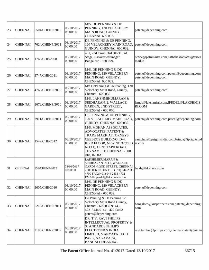
The Patent Office Journal No. 41/2017 Dated 13/10/2017 36715
23 CHENNAI 5504/CHENP/2010 03/10/2017
00:00:00
M/S. DE PENNING & DE
PENNING, 120 VELACHERY
MAIN ROAD, GUINDY,
CHENNAI 600 032.
24 CHENNAI 7624/CHENP/2011 03/10/2017
00:00:00
DE PENNING & DE PENNING,
120 VELACHERY MAIN ROAD,
GUINDY, CHENNAI 600 032.
25 CHENNAI 1763/CHE/2008 03/10/2017
00:00:00
451, 2nd Cross, 3rd Block, 3rd
Stage, Basaveswaranagar,
Bangalore - 560 079.
[email protected],nathanassociates@airtel
mail.in
26 CHENNAI 2747/CHE/2011 03/10/2017
00:00:00
M/S. DE PENNING & DE
PENNING, 120 VELACHERY
MAIN ROAD, GUINDY,
CHENNAI 600 032.
[email protected],[email protected],
27 CHENNAI 4768/CHENP/2009 03/10/2017
00:00:00
M/s DePenning & DePenning, 120,
Velachery Main Road, Guindy,
Chennai - 600 032.
28 CHENNAI 1678/CHENP/2010 03/10/2017
00:00:00
M/S. LAKSHMIKUMARAN &
SRIDHARAN, 2, WALLACE
GARDEN, 2ND STREET,
CHENNAI - 600 006.
[email protected],IPRDEL@LAKSHMIS
RI.COM
29 CHENNAI 7911/CHENP/2011 03/10/2017
00:00:00
DE PENNING & DE PENNING,
120 VELACHERY MAIN ROAD,
GUINDY, CHENNAI 600 032.
[email protected],[email protected]
30 CHENNAI 1542/CHE/2012 03/10/2017
00:00:00
M/S. MOHAN ASSOCIATES,
ADVOCATES, PATENT &
TRADE MARK ATTORNEYS,
CEEBROS BUILDING, D-4,
IIIRD FLOOR, NEW NO.32(OLD
NO.11), CENOTAPH ROAD,
TEYNAMPET, CHENNAI - 600
018, INDIA.
[email protected],brinda@iprightsind
ia.com
31 CHENNAI 159/CHENP/2012 03/10/2017
00:00:00
LAKSHMIKUMARAN &
SRIDHARAN, NO.2, WALLACE
GARDEN, 2ND STREET, CHENNAI
- 600 006. INDIA TEL:(+91) 044 2833
4700 FAX:(+91) 044 2833 4702
EMAIL:[email protected]
32 CHENNAI 2605/CHE/2010 03/10/2017
00:00:00
M/S. DE PENNING & DE
PENNING, 120 VELACHERY
MAIN ROAD, GUINDY,
CHENNAI - 600 032.
33 CHENNAI 5210/CHENP/2011 03/10/2017
00:00:00
De Penning & De Penning 120
Velachery Main Road Guindy,
Chennai - 600 032 9144 -
42213444 9144 - 42213402
[email protected],patent@depenning.
com
34 CHENNAI 2193/CHENP/2009 03/10/2017
00:00:00
DR. T.V. RAVI PHILIPS
INTELLECTUAL PROPERTY &
STANDARDS PHILIPS
ELECTRONICS INDIA
LIMITED, MANYATA TECH
PARK, NAGAVARA,
BANGALORE-560045
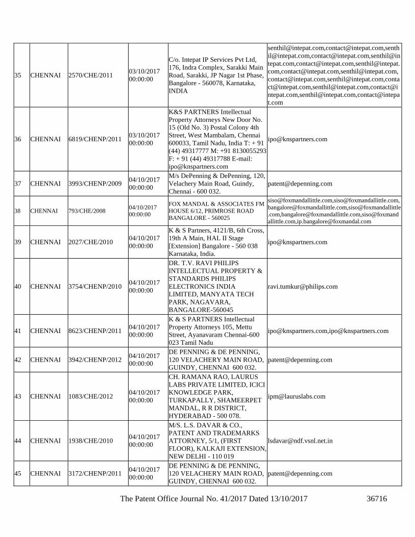
The Patent Office Journal No. 41/2017 Dated 13/10/2017 36716
35 CHENNAI 2570/CHE/2011 03/10/2017
00:00:00
C/o. Intepat IP Services Pvt Ltd,
176, Indra Complex, Sarakki Main
Road, Sarakki, JP Nagar 1st Phase,
Bangalore - 560078, Karnataka,
INDIA
[email protected],[email protected],senth
[email protected],[email protected],senthil@in
tepat.com,[email protected],senthil@intepat.
com,[email protected],[email protected],
[email protected],[email protected],conta
[email protected],[email protected],contact@i
ntepat.com,[email protected],contact@intepa
t.com
36 CHENNAI 6819/CHENP/2011 03/10/2017
00:00:00
K&S PARTNERS Intellectual
Property Attorneys New Door No.
15 (Old No. 3) Postal Colony 4th
Street, West Mambalam, Chennai
600033, Tamil Nadu, India T: + 91
(44) 49317777 M: +91 8130055293
F: + 91 (44) 49317788 E-mail:
37 CHENNAI 3993/CHENP/2009 04/10/2017
00:00:00
M/s DePenning & DePenning, 120,
Velachery Main Road, Guindy,
Chennai - 600 032.
38 CHENNAI 793/CHE/2008 04/10/2017
00:00:00
FOX MANDAL & ASSOCIATES FM
HOUSE 6/12, PRIMROSE ROAD
BANGALORE - 560025
[email protected],[email protected],
[email protected],siso@foxmandallittle
.com,[email protected],siso@foxmand
allittle.com,[email protected]
39 CHENNAI 2027/CHE/2010 04/10/2017
00:00:00
K & S Partners, 4121/B, 6th Cross,
19th A Main, HAL II Stage
[Extension] Bangalore - 560 038
Karnataka, India.
40 CHENNAI 3754/CHENP/2010 04/10/2017
00:00:00
DR. T.V. RAVI PHILIPS
INTELLECTUAL PROPERTY &
STANDARDS PHILIPS
ELECTRONICS INDIA
LIMITED, MANYATA TECH
PARK, NAGAVARA,
BANGALORE-560045
41 CHENNAI 8623/CHENP/2011 04/10/2017
00:00:00
K & S PARTNERS Intellectual
Property Attorneys 105, Mettu
Street, Ayanavaram Chennai-600
023 Tamil Nadu
[email protected],[email protected]
42 CHENNAI 3942/CHENP/2012 04/10/2017
00:00:00
DE PENNING & DE PENNING,
120 VELACHERY MAIN ROAD,
GUINDY, CHENNAI 600 032.
43 CHENNAI 1083/CHE/2012 04/10/2017
00:00:00
CH. RAMANA RAO, LAURUS
LABS PRIVATE LIMITED, ICICI
KNOWLEDGE PARK,
TURKAPALLY, SHAMEERPET
MANDAL, R R DISTRICT,
HYDERABAD - 500 078.
44 CHENNAI 1938/CHE/2010 04/10/2017
00:00:00
M/S. L.S. DAVAR & CO.,
PATENT AND TRADEMARKS
ATTORNEY, 5/1, (FIRST
FLOOR), KALKAJI EXTENSION,
NEW DELHI - 110 019
45 CHENNAI 3172/CHENP/2011 04/10/2017
00:00:00
DE PENNING & DE PENNING,
120 VELACHERY MAIN ROAD,
GUINDY, CHENNAI 600 032.
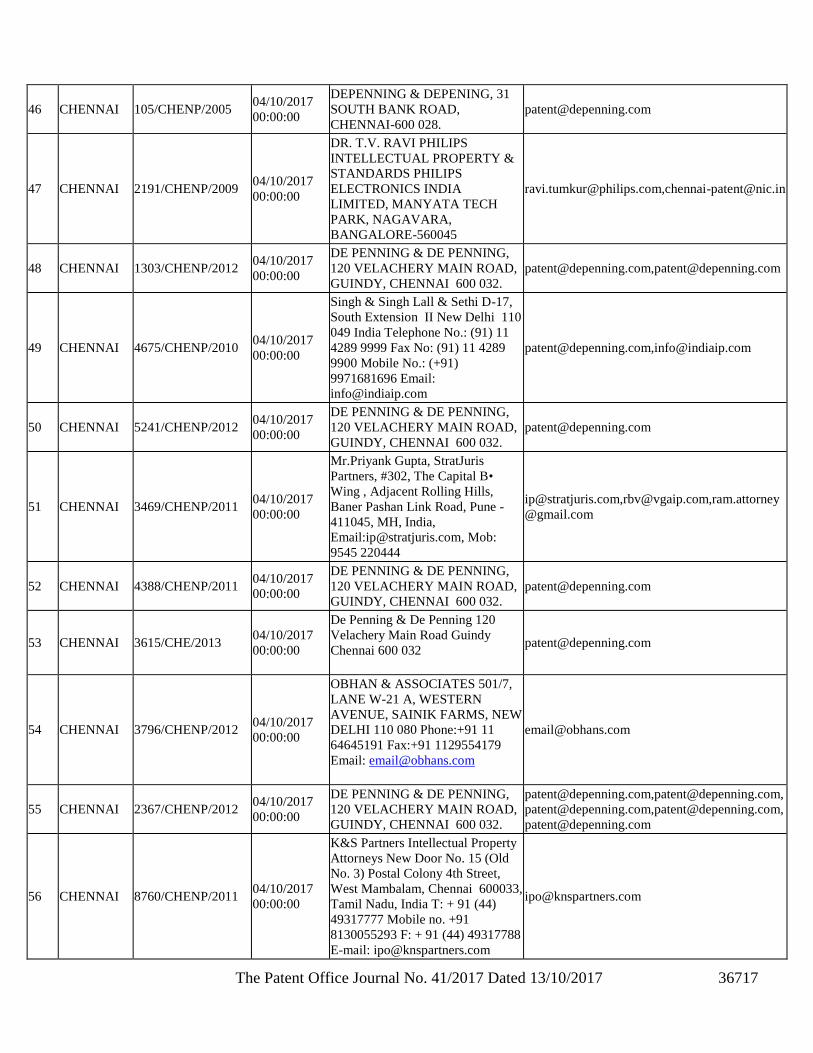
The Patent Office Journal No. 41/2017 Dated 13/10/2017 36717
46 CHENNAI 105/CHENP/2005 04/10/2017
00:00:00
DEPENNING & DEPENING, 31
SOUTH BANK ROAD,
CHENNAI-600 028.
47 CHENNAI 2191/CHENP/2009 04/10/2017
00:00:00
DR. T.V. RAVI PHILIPS
INTELLECTUAL PROPERTY &
STANDARDS PHILIPS
ELECTRONICS INDIA
LIMITED, MANYATA TECH
PARK, NAGAVARA,
BANGALORE-560045
[email protected],[email protected]
48 CHENNAI 1303/CHENP/2012 04/10/2017
00:00:00
DE PENNING & DE PENNING,
120 VELACHERY MAIN ROAD,
GUINDY, CHENNAI 600 032.
[email protected],[email protected]
49 CHENNAI 4675/CHENP/2010 04/10/2017
00:00:00
Singh & Singh Lall & Sethi D-17,
South Extension II New Delhi 110
049 India Telephone No.: (91) 11
4289 9999 Fax No: (91) 11 4289
9900 Mobile No.: (+91)
9971681696 Email:
[email protected],[email protected]
50 CHENNAI 5241/CHENP/2012 04/10/2017
00:00:00
DE PENNING & DE PENNING,
120 VELACHERY MAIN ROAD,
GUINDY, CHENNAI 600 032.
51 CHENNAI 3469/CHENP/2011 04/10/2017
00:00:00
Mr.Priyank Gupta, StratJuris
Partners, #302, The Capital B•
Wing , Adjacent Rolling Hills,
Baner Pashan Link Road, Pune -
411045, MH, India,
Email:[email protected], Mob:
9545 220444
[email protected],[email protected],ram.attorney
@gmail.com
52 CHENNAI 4388/CHENP/2011 04/10/2017
00:00:00
DE PENNING & DE PENNING,
120 VELACHERY MAIN ROAD,
GUINDY, CHENNAI 600 032.
53 CHENNAI 3615/CHE/2013 04/10/2017
00:00:00
De Penning & De Penning 120
Velachery Main Road Guindy
Chennai 600 032
54 CHENNAI 3796/CHENP/2012 04/10/2017
00:00:00
OBHAN & ASSOCIATES 501/7,
LANE W-21 A, WESTERN
AVENUE, SAINIK FARMS, NEW
DELHI 110 080 Phone:+91 11
64645191 Fax:+91 1129554179
Email: [email protected]
55 CHENNAI 2367/CHENP/2012 04/10/2017
00:00:00
DE PENNING & DE PENNING,
120 VELACHERY MAIN ROAD,
GUINDY, CHENNAI 600 032.
[email protected],[email protected],
[email protected],[email protected],
56 CHENNAI 8760/CHENP/2011 04/10/2017
00:00:00
K&S Partners Intellectual Property
Attorneys New Door No. 15 (Old
No. 3) Postal Colony 4th Street,
West Mambalam, Chennai 600033,
Tamil Nadu, India T: + 91 (44)
49317777 Mobile no. +91
8130055293 F: + 91 (44) 49317788
E-mail: [email protected]
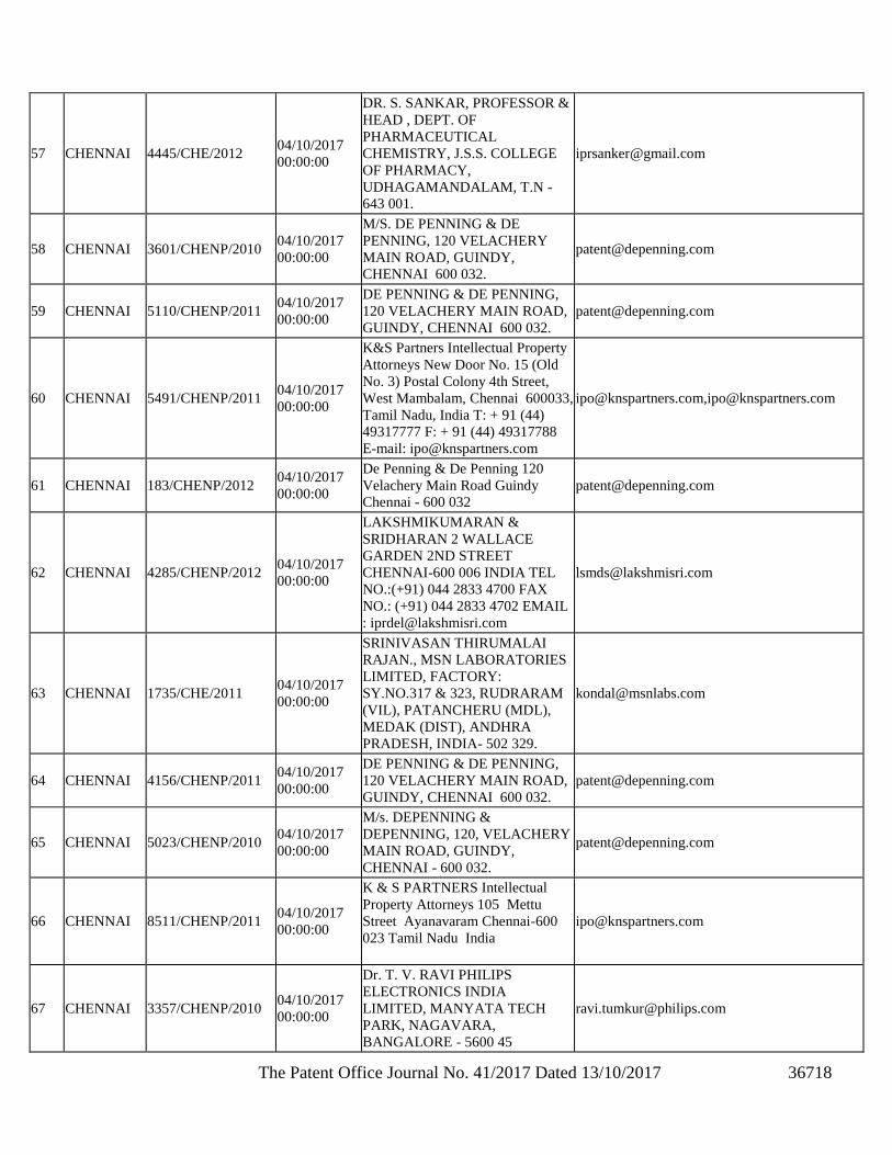
The Patent Office Journal No. 41/2017 Dated 13/10/2017 36718
57 CHENNAI 4445/CHE/2012 04/10/2017
00:00:00
DR. S. SANKAR, PROFESSOR &
HEAD , DEPT. OF
PHARMACEUTICAL
CHEMISTRY, J.S.S. COLLEGE
OF PHARMACY,
UDHAGAMANDALAM, T.N -
643 001.
58 CHENNAI 3601/CHENP/2010 04/10/2017
00:00:00
M/S. DE PENNING & DE
PENNING, 120 VELACHERY
MAIN ROAD, GUINDY,
CHENNAI 600 032.
59 CHENNAI 5110/CHENP/2011 04/10/2017
00:00:00
DE PENNING & DE PENNING,
120 VELACHERY MAIN ROAD,
GUINDY, CHENNAI 600 032.
60 CHENNAI 5491/CHENP/2011 04/10/2017
00:00:00
K&S Partners Intellectual Property
Attorneys New Door No. 15 (Old
No. 3) Postal Colony 4th Street,
West Mambalam, Chennai 600033,
Tamil Nadu, India T: + 91 (44)
49317777 F: + 91 (44) 49317788
E-mail: [email protected]
[email protected],[email protected]
61 CHENNAI 183/CHENP/2012 04/10/2017
00:00:00
De Penning & De Penning 120
Velachery Main Road Guindy
Chennai - 600 032
62 CHENNAI 4285/CHENP/2012 04/10/2017
00:00:00
LAKSHMIKUMARAN &
SRIDHARAN 2 WALLACE
GARDEN 2ND STREET
CHENNAI-600 006 INDIA TEL
NO.:(+91) 044 2833 4700 FAX
NO.: (+91) 044 2833 4702 EMAIL
63 CHENNAI 1735/CHE/2011 04/10/2017
00:00:00
SRINIVASAN THIRUMALAI
RAJAN., MSN LABORATORIES
LIMITED, FACTORY:
SY.NO.317 & 323, RUDRARAM
(VIL), PATANCHERU (MDL),
MEDAK (DIST), ANDHRA
PRADESH, INDIA- 502 329.
64 CHENNAI 4156/CHENP/2011 04/10/2017
00:00:00
DE PENNING & DE PENNING,
120 VELACHERY MAIN ROAD,
GUINDY, CHENNAI 600 032.
65 CHENNAI 5023/CHENP/2010 04/10/2017
00:00:00
M/s. DEPENNING &
DEPENNING, 120, VELACHERY
MAIN ROAD, GUINDY,
CHENNAI - 600 032.
66 CHENNAI 8511/CHENP/2011 04/10/2017
00:00:00
K & S PARTNERS Intellectual
Property Attorneys 105 Mettu
Street Ayanavaram Chennai-600
023 Tamil Nadu India
67 CHENNAI 3357/CHENP/2010 04/10/2017
00:00:00
Dr. T. V. RAVI PHILIPS
ELECTRONICS INDIA
LIMITED, MANYATA TECH
PARK, NAGAVARA,
BANGALORE - 5600 45
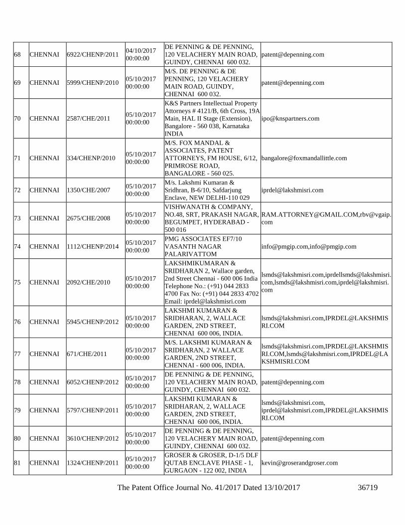
The Patent Office Journal No. 41/2017 Dated 13/10/2017 36719
68 CHENNAI 6922/CHENP/2011 04/10/2017
00:00:00
DE PENNING & DE PENNING,
120 VELACHERY MAIN ROAD,
GUINDY, CHENNAI 600 032.
69 CHENNAI 5999/CHENP/2010 05/10/2017
00:00:00
M/S. DE PENNING & DE
PENNING, 120 VELACHERY
MAIN ROAD, GUINDY,
CHENNAI 600 032.
70 CHENNAI 2587/CHE/2011 05/10/2017
00:00:00
K&S Partners Intellectual Property
Attorneys # 4121/B, 6th Cross, 19A
Main, HAL II Stage (Extension),
Bangalore - 560 038, Karnataka
INDIA
71 CHENNAI 334/CHENP/2010 05/10/2017
00:00:00
M/S. FOX MANDAL &
ASSOCIATES, PATENT
ATTORNEYS, FM HOUSE, 6/12,
PRIMROSE ROAD,
BANGALORE - 560 025.
72 CHENNAI 1350/CHE/2007 05/10/2017
00:00:00
M/s. Lakshmi Kumaran &
Sridhran, B-6/10, Safdarjung
Enclave, NEW DELHI-110 029
73 CHENNAI 2675/CHE/2008 05/10/2017
00:00:00
VISHWANATH & COMPANY,
NO.48, SRT, PRAKASH NAGAR,
BEGUMPET, HYDERABAD -
500 016
[email protected],rbv@vgaip.
com
74 CHENNAI 1112/CHENP/2014 05/10/2017
00:00:00
PMG ASSOCIATES EF7/10
VASANTH NAGAR
PALARIVATTOM
[email protected],[email protected]
75 CHENNAI 2092/CHE/2010 05/10/2017
00:00:00
LAKSHMIKUMARAN &
SRIDHARAN 2, Wallace garden,
2nd Street Chennai - 600 006 India
Telephone No.: (+91) 044 2833
4700 Fax No: (+91) 044 2833 4702
Email: [email protected]
[email protected],iprdellsmds@lakshmisri.
com,[email protected],iprdel@lakshmisri.
com
76 CHENNAI 5945/CHENP/2012 05/10/2017
00:00:00
LAKSHMI KUMARAN &
SRIDHARAN, 2, WALLACE
GARDEN, 2ND STREET,
CHENNAI 600 006, INDIA.
[email protected],IPRDEL@LAKSHMIS
RI.COM
77 CHENNAI 671/CHE/2011 05/10/2017
00:00:00
M/S. LAKSHMI KUMARAN &
SRIDHARAN, 2 WALLACE
GARDEN, 2ND STREET,
CHENNAI - 600 006, INDIA.
[email protected],IPRDEL@LAKSHMIS
RI.COM,[email protected],IPRDEL@LA
KSHMISRI.COM
78 CHENNAI 6052/CHENP/2012 05/10/2017
00:00:00
DE PENNING & DE PENNING,
120 VELACHERY MAIN ROAD,
GUINDY, CHENNAI 600 032.
79 CHENNAI 5797/CHENP/2011 05/10/2017
00:00:00
LAKSHMI KUMARAN &
SRIDHARAN, 2, WALLACE
GARDEN, 2ND STREET,
CHENNAI 600 006, INDIA.
[email protected],IPRDEL@LAKSHMIS
RI.COM
80 CHENNAI 3610/CHENP/2012 05/10/2017
00:00:00
DE PENNING & DE PENNING,
120 VELACHERY MAIN ROAD,
GUINDY, CHENNAI 600 032.
81 CHENNAI 1324/CHENP/2011 05/10/2017
00:00:00
GROSER & GROSER, D-1/5 DLF
QUTAB ENCLAVE PHASE - 1,
GURGAON - 122 002, INDIA
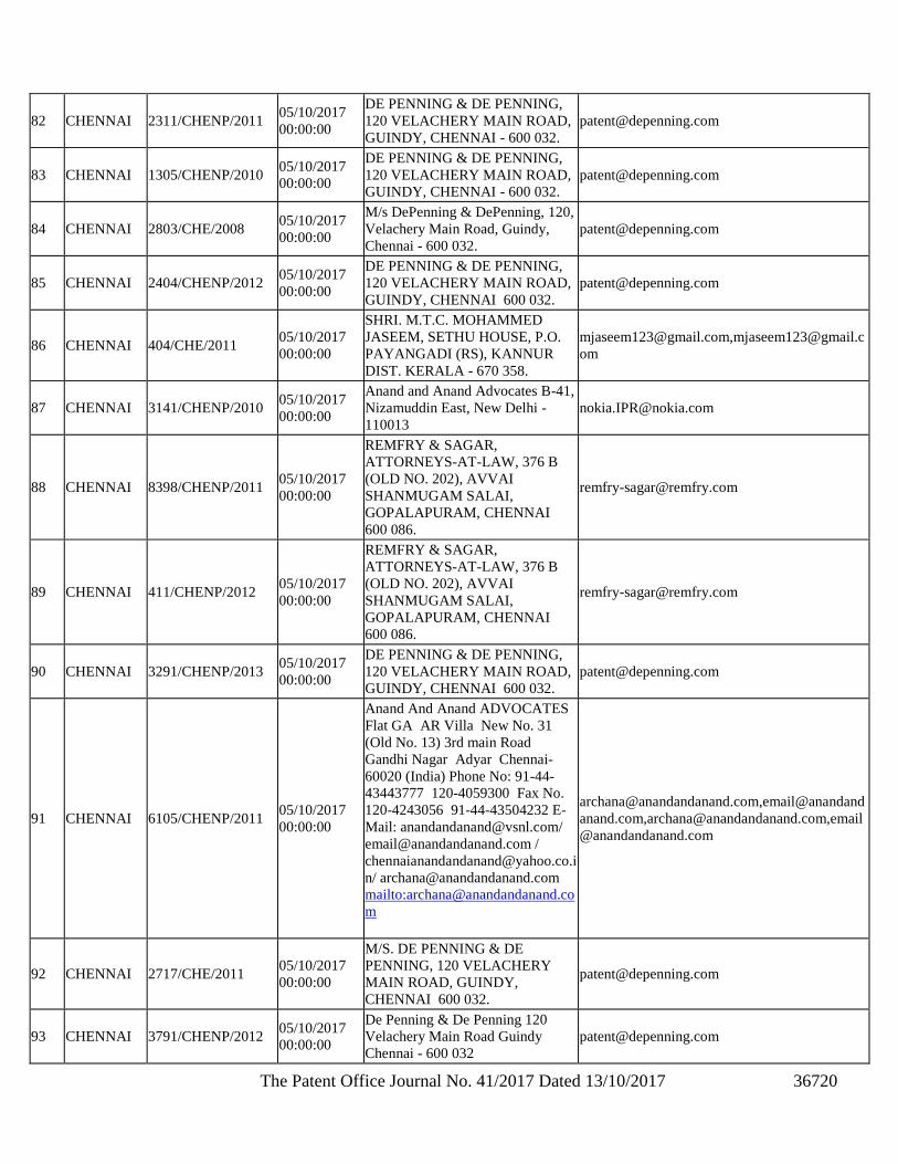
The Patent Office Journal No. 41/2017 Dated 13/10/2017 36720
82 CHENNAI 2311/CHENP/2011 05/10/2017
00:00:00
DE PENNING & DE PENNING,
120 VELACHERY MAIN ROAD,
GUINDY, CHENNAI - 600 032.
83 CHENNAI 1305/CHENP/2010 05/10/2017
00:00:00
DE PENNING & DE PENNING,
120 VELACHERY MAIN ROAD,
GUINDY, CHENNAI - 600 032.
84 CHENNAI 2803/CHE/2008 05/10/2017
00:00:00
M/s DePenning & DePenning, 120,
Velachery Main Road, Guindy,
Chennai - 600 032.
85 CHENNAI 2404/CHENP/2012 05/10/2017
00:00:00
DE PENNING & DE PENNING,
120 VELACHERY MAIN ROAD,
GUINDY, CHENNAI 600 032.
86 CHENNAI 404/CHE/2011 05/10/2017
00:00:00
SHRI. M.T.C. MOHAMMED
JASEEM, SETHU HOUSE, P.O.
PAYANGADI (RS), KANNUR
DIST. KERALA - 670 358.
[email protected],[email protected]
om
87 CHENNAI 3141/CHENP/2010 05/10/2017
00:00:00
Anand and Anand Advocates B-41,
Nizamuddin East, New Delhi -
110013
88 CHENNAI 8398/CHENP/2011 05/10/2017
00:00:00
REMFRY & SAGAR,
ATTORNEYS-AT-LAW, 376 B
(OLD NO. 202), AVVAI
SHANMUGAM SALAI,
GOPALAPURAM, CHENNAI
600 086.
89 CHENNAI 411/CHENP/2012 05/10/2017
00:00:00
REMFRY & SAGAR,
ATTORNEYS-AT-LAW, 376 B
(OLD NO. 202), AVVAI
SHANMUGAM SALAI,
GOPALAPURAM, CHENNAI
600 086.
90 CHENNAI 3291/CHENP/2013 05/10/2017
00:00:00
DE PENNING & DE PENNING,
120 VELACHERY MAIN ROAD,
GUINDY, CHENNAI 600 032.
91 CHENNAI 6105/CHENP/2011 05/10/2017
00:00:00
Anand And Anand ADVOCATES
Flat GA AR Villa New No. 31
(Old No. 13) 3rd main Road
Gandhi Nagar Adyar Chennai-
60020 (India) Phone No: 91-44-
43443777 120-4059300 Fax No.
120-4243056 91-44-43504232 E-
Mail: [email protected]/
mailto:[email protected]
m
[email protected],email@anandand
anand.com,[email protected],email
@anandandanand.com
92 CHENNAI 2717/CHE/2011 05/10/2017
00:00:00
M/S. DE PENNING & DE
PENNING, 120 VELACHERY
MAIN ROAD, GUINDY,
CHENNAI 600 032.
93 CHENNAI 3791/CHENP/2012 05/10/2017
00:00:00
De Penning & De Penning 120
Velachery Main Road Guindy
Chennai - 600 032
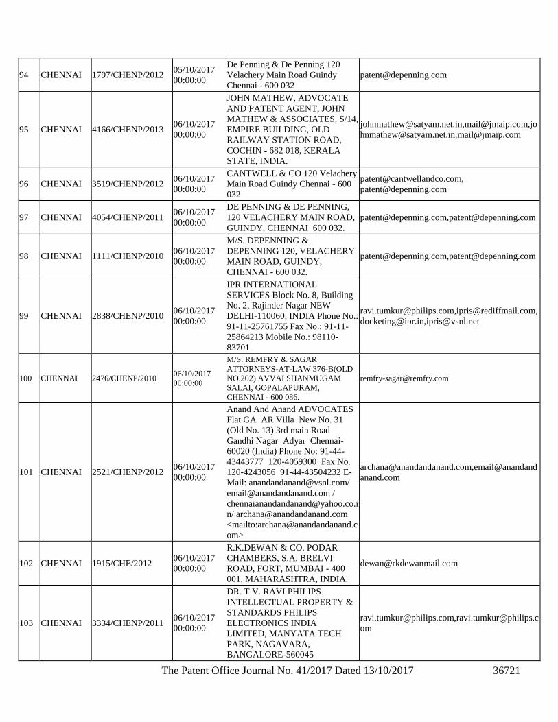
The Patent Office Journal No. 41/2017 Dated 13/10/2017 36721
94 CHENNAI 1797/CHENP/2012 05/10/2017
00:00:00
De Penning & De Penning 120
Velachery Main Road Guindy
Chennai - 600 032
95 CHENNAI 4166/CHENP/2013 06/10/2017
00:00:00
JOHN MATHEW, ADVOCATE
AND PATENT AGENT, JOHN
MATHEW & ASSOCIATES, S/14,
EMPIRE BUILDING, OLD
RAILWAY STATION ROAD,
COCHIN - 682 018, KERALA
STATE, INDIA.
[email protected],[email protected],jo
[email protected],[email protected]
96 CHENNAI 3519/CHENP/2012 06/10/2017
00:00:00
CANTWELL & CO 120 Velachery
Main Road Guindy Chennai - 600
032
97 CHENNAI 4054/CHENP/2011 06/10/2017
00:00:00
DE PENNING & DE PENNING,
120 VELACHERY MAIN ROAD,
GUINDY, CHENNAI 600 032.
[email protected],[email protected]
98 CHENNAI 1111/CHENP/2010 06/10/2017
00:00:00
M/S. DEPENNING &
DEPENNING 120, VELACHERY
MAIN ROAD, GUINDY,
CHENNAI - 600 032.
[email protected],[email protected]
99 CHENNAI 2838/CHENP/2010 06/10/2017
00:00:00
IPR INTERNATIONAL
SERVICES Block No. 8, Building
No. 2, Rajinder Nagar NEW
DELHI-110060, INDIA Phone No.:
91-11-25761755 Fax No.: 91-11-
25864213 Mobile No.: 98110-
83701
[email protected],[email protected],
[email protected],[email protected]
100 CHENNAI 2476/CHENP/2010 06/10/2017
00:00:00
M/S. REMFRY & SAGAR
ATTORNEYS-AT-LAW 376-B(OLD
NO.202) AVVAI SHANMUGAM
SALAI, GOPALAPURAM,
CHENNAI - 600 086.
101 CHENNAI 2521/CHENP/2012 06/10/2017
00:00:00
Anand And Anand ADVOCATES
Flat GA AR Villa New No. 31
(Old No. 13) 3rd main Road
Gandhi Nagar Adyar Chennai-
60020 (India) Phone No: 91-44-
43443777 120-4059300 Fax No.
120-4243056 91-44-43504232 E-
Mail: [email protected]/
<mailto:[email protected]
om>
[email protected],email@anandand
anand.com
102 CHENNAI 1915/CHE/2012 06/10/2017
00:00:00
R.K.DEWAN & CO. PODAR
CHAMBERS, S.A. BRELVI
ROAD, FORT, MUMBAI - 400
001, MAHARASHTRA, INDIA.
103 CHENNAI 3334/CHENP/2011 06/10/2017
00:00:00
DR. T.V. RAVI PHILIPS
INTELLECTUAL PROPERTY &
STANDARDS PHILIPS
ELECTRONICS INDIA
LIMITED, MANYATA TECH
PARK, NAGAVARA,
BANGALORE-560045
[email protected],[email protected]
om
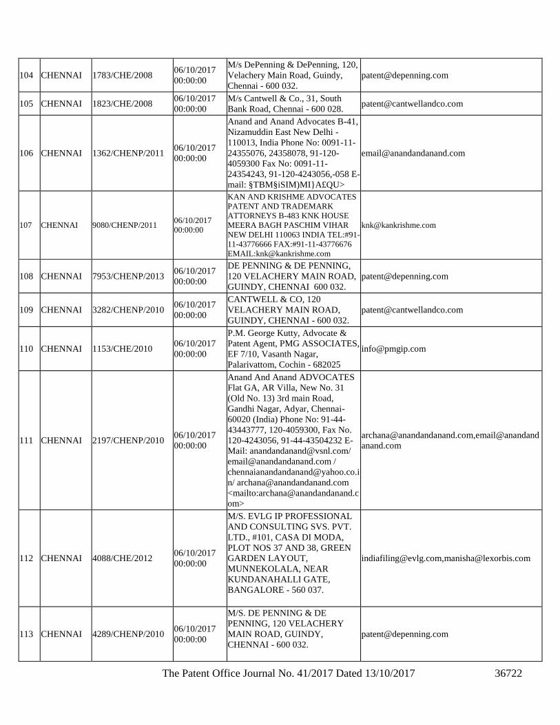
The Patent Office Journal No. 41/2017 Dated 13/10/2017 36722
104 CHENNAI 1783/CHE/2008 06/10/2017
00:00:00
M/s DePenning & DePenning, 120,
Velachery Main Road, Guindy,
Chennai - 600 032.
105 CHENNAI 1823/CHE/2008 06/10/2017
00:00:00
M/s Cantwell & Co., 31, South
Bank Road, Chennai - 600 028. [email protected]
106 CHENNAI 1362/CHENP/2011 06/10/2017
00:00:00
Anand and Anand Advocates B-41,
Nizamuddin East New Delhi -
110013, India Phone No: 0091-11-
24355076, 24358078, 91-120-
4059300 Fax No: 0091-11-
24354243, 91-120-4243056,-058 E-
mail: §TBM§iSIM)MI}A£QU>
107 CHENNAI 9080/CHENP/2011 06/10/2017
00:00:00
KAN AND KRISHME ADVOCATES
PATENT AND TRADEMARK
ATTORNEYS B-483 KNK HOUSE
MEERA BAGH PASCHIM VIHAR
NEW DELHI 110063 INDIA TEL:#91-
11-43776666 FAX:#91-11-43776676
EMAIL:[email protected]
108 CHENNAI 7953/CHENP/2013 06/10/2017
00:00:00
DE PENNING & DE PENNING,
120 VELACHERY MAIN ROAD,
GUINDY, CHENNAI 600 032.
109 CHENNAI 3282/CHENP/2010 06/10/2017
00:00:00
CANTWELL & CO, 120
VELACHERY MAIN ROAD,
GUINDY, CHENNAI - 600 032.
110 CHENNAI 1153/CHE/2010 06/10/2017
00:00:00
P.M. George Kutty, Advocate &
Patent Agent, PMG ASSOCIATES,
EF 7/10, Vasanth Nagar,
Palarivattom, Cochin - 682025
111 CHENNAI 2197/CHENP/2010 06/10/2017
00:00:00
Anand And Anand ADVOCATES
Flat GA, AR Villa, New No. 31
(Old No. 13) 3rd main Road,
Gandhi Nagar, Adyar, Chennai-
60020 (India) Phone No: 91-44-
43443777, 120-4059300, Fax No.
120-4243056, 91-44-43504232 E-
Mail: [email protected]/
<mailto:[email protected]
om>
[email protected],email@anandand
anand.com
112 CHENNAI 4088/CHE/2012 06/10/2017
00:00:00
M/S. EVLG IP PROFESSIONAL
AND CONSULTING SVS. PVT.
LTD., #101, CASA DI MODA,
PLOT NOS 37 AND 38, GREEN
GARDEN LAYOUT,
MUNNEKOLALA, NEAR
KUNDANAHALLI GATE,
BANGALORE - 560 037.
[email protected],[email protected]
113 CHENNAI 4289/CHENP/2010 06/10/2017
00:00:00
M/S. DE PENNING & DE
PENNING, 120 VELACHERY
MAIN ROAD, GUINDY,
CHENNAI - 600 032.
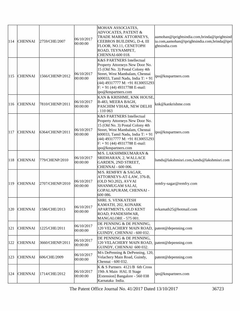
The Patent Office Journal No. 41/2017 Dated 13/10/2017 36723
114 CHENNAI 2759/CHE/2007 06/10/2017
00:00:00
MOHAN ASSOCIATES,
ADVOCATES, PATENT &
TRADE MARK ATTORNEYS,
CEEBROS BUILDING, D-4, III
FLOOR, NO.11, CENETOPH
ROAD, TEYNAMPET,
CHENNAI-600 018.
[email protected],brinda@iprightsind
ia.com,[email protected],brinda@ipri
ghtsindia.com
115 CHENNAI 1566/CHENP/2012 06/10/2017
00:00:00
K&S PARTNERS Intellectual
Property Attorneys New Door No.
15 (Old No. 3) Postal Colony 4th
Street, West Mambalam, Chennai
600033, Tamil Nadu, India T: + 91
(44) 49317777 M: +91 8130055293
F: + 91 (44) 49317788 E-mail:
116 CHENNAI 7810/CHENP/2011 06/10/2017
00:00:00
KAN & KRISHME, KNK HOUSE,
B-483, MEERA BAGH,
PASCHIM VIHAR, NEW DELHI
- 110 063
117 CHENNAI 6364/CHENP/2011 06/10/2017
00:00:00
K&S PARTNERS Intellectual
Property Attorneys New Door No.
15 (Old No. 3) Postal Colony 4th
Street, West Mambalam, Chennai
600033, Tamil Nadu, India T: + 91
(44) 49317777 M: +91 8130055293
F: + 91 (44) 49317788 E-mail:
118 CHENNAI 779/CHENP/2010 06/10/2017
00:00:00
M/S. LAKSHMIKUMARAN &
SRIDHARAN, 2, WALLACE
GARDEN, 2ND STREET,
CHENNAI - 600 006.
[email protected],[email protected]
119 CHENNAI 2707/CHENP/2010 06/10/2017
00:00:00
M/S. REMFRY & SAGAR,
ATTORNEYS-AT-LAW, 376-B,
(OLD NO.202), AVVAI
SHANMUGAM SALAI,
GOPALAPURAM, CHENNAI -
600 086.
120 CHENNAI 1586/CHE/2013 06/10/2017
00:00:00
SHRI. S. VENKATESH
KAMATH, 202, KONARK
APARTMENTS, OLD KENT
ROAD, PANDESHWAR,
MANGALORE - 575 001.
121 CHENNAI 1225/CHE/2011 06/10/2017
00:00:00
DE PENNING & DE PENNING,
120 VELACHERY MAIN ROAD,
GUINDY, CHENNAI - 600 032.
122 CHENNAI 3660/CHENP/2011 06/10/2017
00:00:00
DE PENNING & DE PENNING,
120 VELACHERY MAIN ROAD,
GUINDY, CHENNAI 600 032.
123 CHENNAI 606/CHE/2009 06/10/2017
00:00:00
M/s DePenning & DePenning, 120,
Velachery Main Road, Guindy,
Chennai - 600 032.
124 CHENNAI 1714/CHE/2012 06/10/2017
00:00:00
K & S Partners 4121/B 6th Cross
19th A Main HAL II Stage
[Extension] Bangalore - 560 038
Karnataka India.
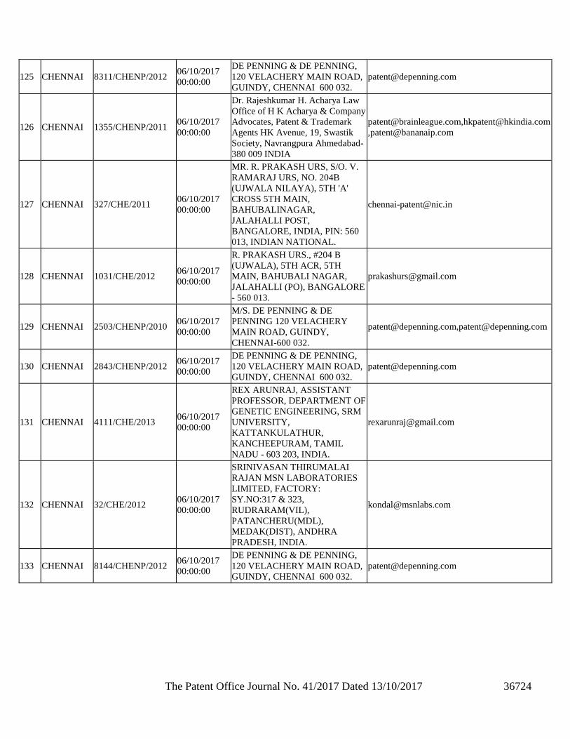
The Patent Office Journal No. 41/2017 Dated 13/10/2017 36724
125 CHENNAI 8311/CHENP/2012 06/10/2017
00:00:00
DE PENNING & DE PENNING,
120 VELACHERY MAIN ROAD,
GUINDY, CHENNAI 600 032.
126 CHENNAI 1355/CHENP/2011 06/10/2017
00:00:00
Dr. Rajeshkumar H. Acharya Law
Office of H K Acharya & Company
Advocates, Patent & Trademark
Agents HK Avenue, 19, Swastik
Society, Navrangpura Ahmedabad-
380 009 INDIA
[email protected],[email protected]
127 CHENNAI 327/CHE/2011 06/10/2017
00:00:00
MR. R. PRAKASH URS, S/O. V.
RAMARAJ URS, NO. 204B
(UJWALA NILAYA), 5TH 'A'
CROSS 5TH MAIN,
BAHUBALINAGAR,
JALAHALLI POST,
BANGALORE, INDIA, PIN: 560
013, INDIAN NATIONAL.
128 CHENNAI 1031/CHE/2012 06/10/2017
00:00:00
R. PRAKASH URS., #204 B
(UJWALA), 5TH ACR, 5TH
MAIN, BAHUBALI NAGAR,
JALAHALLI (PO), BANGALORE
- 560 013.
129 CHENNAI 2503/CHENP/2010 06/10/2017
00:00:00
M/S. DE PENNING & DE
PENNING 120 VELACHERY
MAIN ROAD, GUINDY,
CHENNAI-600 032.
[email protected],[email protected]
130 CHENNAI 2843/CHENP/2012 06/10/2017
00:00:00
DE PENNING & DE PENNING,
120 VELACHERY MAIN ROAD,
GUINDY, CHENNAI 600 032.
131 CHENNAI 4111/CHE/2013 06/10/2017
00:00:00
REX ARUNRAJ, ASSISTANT
PROFESSOR, DEPARTMENT OF
GENETIC ENGINEERING, SRM
UNIVERSITY,
KATTANKULATHUR,
KANCHEEPURAM, TAMIL
NADU - 603 203, INDIA.
132 CHENNAI 32/CHE/2012 06/10/2017
00:00:00
SRINIVASAN THIRUMALAI
RAJAN MSN LABORATORIES
LIMITED, FACTORY:
SY.NO:317 & 323,
RUDRARAM(VIL),
PATANCHERU(MDL),
MEDAK(DIST), ANDHRA
PRADESH, INDIA.
133 CHENNAI 8144/CHENP/2012 06/10/2017
00:00:00
DE PENNING & DE PENNING,
120 VELACHERY MAIN ROAD,
GUINDY, CHENNAI 600 032.
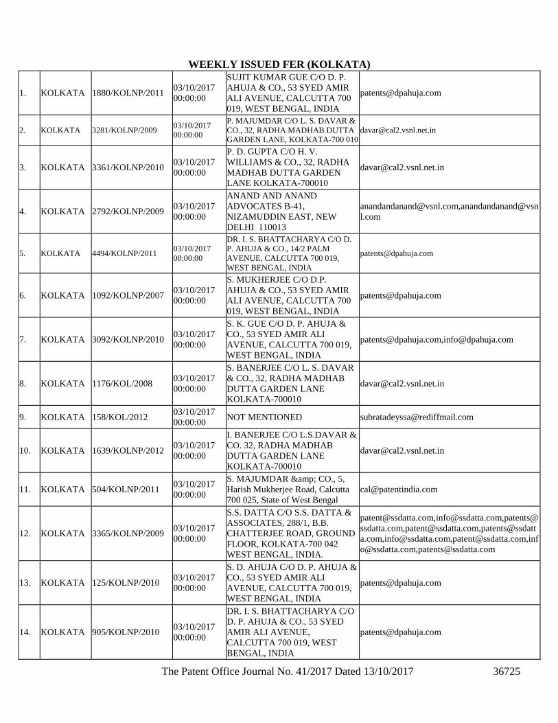
The Patent Office Journal No. 41/2017 Dated 13/10/2017 36725
WEEKLY ISSUED FER (KOLKATA)
1. KOLKATA 1880/KOLNP/2011 03/10/2017
00:00:00
SUJIT KUMAR GUE C/O D. P.
AHUJA & CO., 53 SYED AMIR
ALI AVENUE, CALCUTTA 700
019, WEST BENGAL, INDIA
2. KOLKATA 3281/KOLNP/2009 03/10/2017
00:00:00
P. MAJUMDAR C/O L. S. DAVAR &
CO., 32, RADHA MADHAB DUTTA
GARDEN LANE, KOLKATA-700 010
3. KOLKATA 3361/KOLNP/2010 03/10/2017
00:00:00
P. D. GUPTA C/O H. V.
WILLIAMS & CO., 32, RADHA
MADHAB DUTTA GARDEN
LANE KOLKATA-700010
4. KOLKATA 2792/KOLNP/2009 03/10/2017
00:00:00
ANAND AND ANAND
ADVOCATES B-41,
NIZAMUDDIN EAST, NEW
DELHI 110013
[email protected],anandandanand@vsn
l.com
5. KOLKATA 4494/KOLNP/2011 03/10/2017
00:00:00
DR. I. S. BHATTACHARYA C/O D.
P. AHUJA & CO., 14/2 PALM
AVENUE, CALCUTTA 700 019,
WEST BENGAL, INDIA
6. KOLKATA 1092/KOLNP/2007 03/10/2017
00:00:00
S. MUKHERJEE C/O D.P.
AHUJA & CO., 53 SYED AMIR
ALI AVENUE, CALCUTTA 700
019, WEST BENGAL, INDIA
7. KOLKATA 3092/KOLNP/2010 03/10/2017
00:00:00
S. K. GUE C/O D. P. AHUJA &
CO., 53 SYED AMIR ALI
AVENUE, CALCUTTA 700 019,
WEST BENGAL, INDIA
[email protected],[email protected]
8. KOLKATA 1176/KOL/2008 03/10/2017
00:00:00
S. BANERJEE C/O L. S. DAVAR
& CO., 32, RADHA MADHAB
DUTTA GARDEN LANE
KOLKATA-700010
9. KOLKATA 158/KOL/2012 03/10/2017
00:00:00 NOT MENTIONED [email protected]
10. KOLKATA 1639/KOLNP/2012 03/10/2017
00:00:00
I. BANERJEE C/O L.S.DAVAR &
CO. 32, RADHA MADHAB
DUTTA GARDEN LANE
KOLKATA-700010
11. KOLKATA 504/KOLNP/2011 03/10/2017
00:00:00
S. MAJUMDAR & CO., 5,
Harish Mukherjee Road, Calcutta
700 025, State of West Bengal
12. KOLKATA 3365/KOLNP/2009 03/10/2017
00:00:00
S.S. DATTA C/O S.S. DATTA &
ASSOCIATES, 288/1, B.B.
CHATTERJEE ROAD, GROUND
FLOOR, KOLKATA-700 042
WEST BENGAL, INDIA.
[email protected],[email protected],patents@
ssdatta.com,[email protected],patents@ssdatt
a.com,[email protected],[email protected],inf
[email protected],[email protected]
13. KOLKATA 125/KOLNP/2010 03/10/2017
00:00:00
S. D. AHUJA C/O D. P. AHUJA &
CO., 53 SYED AMIR ALI
AVENUE, CALCUTTA 700 019,
WEST BENGAL, INDIA
14. KOLKATA 905/KOLNP/2010 03/10/2017
00:00:00
DR. I. S. BHATTACHARYA C/O
D. P. AHUJA & CO., 53 SYED
AMIR ALI AVENUE,
CALCUTTA 700 019, WEST
BENGAL, INDIA
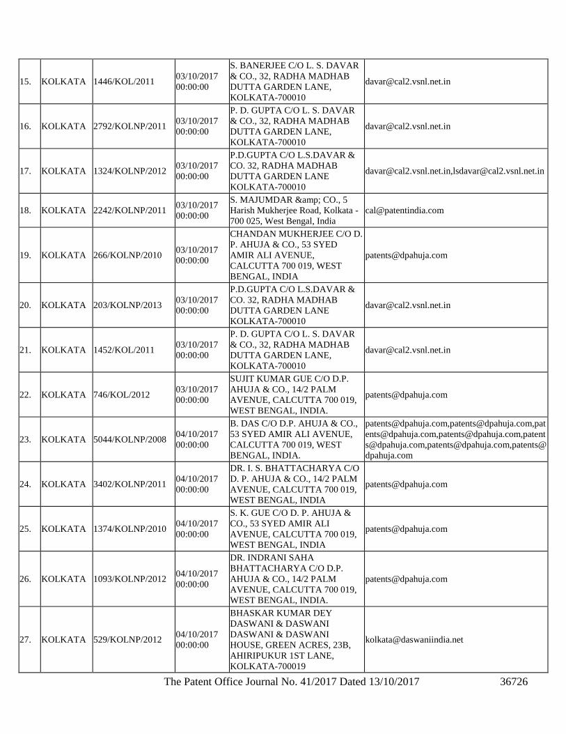
The Patent Office Journal No. 41/2017 Dated 13/10/2017 36726
15. KOLKATA 1446/KOL/2011 03/10/2017
00:00:00
S. BANERJEE C/O L. S. DAVAR
& CO., 32, RADHA MADHAB
DUTTA GARDEN LANE,
KOLKATA-700010
16. KOLKATA 2792/KOLNP/2011 03/10/2017
00:00:00
P. D. GUPTA C/O L. S. DAVAR
& CO., 32, RADHA MADHAB
DUTTA GARDEN LANE,
KOLKATA-700010
17. KOLKATA 1324/KOLNP/2012 03/10/2017
00:00:00
P.D.GUPTA C/O L.S.DAVAR &
CO. 32, RADHA MADHAB
DUTTA GARDEN LANE
KOLKATA-700010
[email protected],[email protected]
18. KOLKATA 2242/KOLNP/2011 03/10/2017
00:00:00
S. MAJUMDAR & CO., 5
Harish Mukherjee Road, Kolkata -
700 025, West Bengal, India
19. KOLKATA 266/KOLNP/2010 03/10/2017
00:00:00
CHANDAN MUKHERJEE C/O D.
P. AHUJA & CO., 53 SYED
AMIR ALI AVENUE,
CALCUTTA 700 019, WEST
BENGAL, INDIA
20. KOLKATA 203/KOLNP/2013 03/10/2017
00:00:00
P.D.GUPTA C/O L.S.DAVAR &
CO. 32, RADHA MADHAB
DUTTA GARDEN LANE
KOLKATA-700010
21. KOLKATA 1452/KOL/2011 03/10/2017
00:00:00
P. D. GUPTA C/O L. S. DAVAR
& CO., 32, RADHA MADHAB
DUTTA GARDEN LANE,
KOLKATA-700010
22. KOLKATA 746/KOL/2012 03/10/2017
00:00:00
SUJIT KUMAR GUE C/O D.P.
AHUJA & CO., 14/2 PALM
AVENUE, CALCUTTA 700 019,
WEST BENGAL, INDIA.
23. KOLKATA 5044/KOLNP/2008 04/10/2017
00:00:00
B. DAS C/O D.P. AHUJA & CO.,
53 SYED AMIR ALI AVENUE,
CALCUTTA 700 019, WEST
BENGAL, INDIA.
[email protected],[email protected],pat
[email protected],[email protected],patent
[email protected],[email protected],patents@
dpahuja.com
24. KOLKATA 3402/KOLNP/2011 04/10/2017
00:00:00
DR. I. S. BHATTACHARYA C/O
D. P. AHUJA & CO., 14/2 PALM
AVENUE, CALCUTTA 700 019,
WEST BENGAL, INDIA
25. KOLKATA 1374/KOLNP/2010 04/10/2017
00:00:00
S. K. GUE C/O D. P. AHUJA &
CO., 53 SYED AMIR ALI
AVENUE, CALCUTTA 700 019,
WEST BENGAL, INDIA
26. KOLKATA 1093/KOLNP/2012 04/10/2017
00:00:00
DR. INDRANI SAHA
BHATTACHARYA C/O D.P.
AHUJA & CO., 14/2 PALM
AVENUE, CALCUTTA 700 019,
WEST BENGAL, INDIA.
27. KOLKATA 529/KOLNP/2012 04/10/2017
00:00:00
BHASKAR KUMAR DEY
DASWANI & DASWANI
DASWANI & DASWANI
HOUSE, GREEN ACRES, 23B,
AHIRIPUKUR 1ST LANE,
KOLKATA-700019
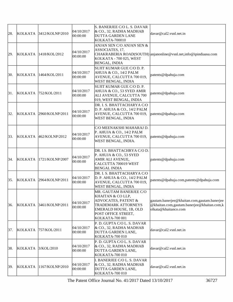
The Patent Office Journal No. 41/2017 Dated 13/10/2017 36727
28. KOLKATA 3412/KOLNP/2010 04/10/2017
00:00:00
S. BANERJEE C/O L. S. DAVAR
& CO., 32, RADHA MADHAB
DUTTA GARDEN LANE
KOLKATA-700010
29. KOLKATA 1418/KOL/2012 04/10/2017
00:00:00
ANJAN SEN C/O ANJAN SEN &
ASSOCIATES, 17,
CHAKRABERIA ROAD(SOUTH)
KOLKATA - 700 025, WEST
BENGAL, INDIA
[email protected],[email protected]
30. KOLKATA 1464/KOL/2011 04/10/2017
00:00:00
SUJIT KUMAR GUE C/O D. P.
AHUJA & CO., 14/2 PALM
AVENUE, CALCUTTA 700 019,
WEST BENGAL, INDIA
31. KOLKATA 752/KOL/2011 04/10/2017
00:00:00
SUJIT KUMAR GUE C/O D. P.
AHUJA & CO., 53 SYED AMIR
ALI AVENUE, CALCUTTA 700
019, WEST BENGAL, INDIA
32. KOLKATA 2960/KOLNP/2011 04/10/2017
00:00:00
DR. I. S. BHATTACHARYA C/O
D. P. AHUJA & CO., 14/2 PALM
AVENUE, CALCUTTA 700 019,
WEST BENGAL, INDIA
33. KOLKATA 462/KOLNP/2012 04/10/2017
00:00:00
C/O MEENAKSHI MAHARAJ D.
P. AHUJA & CO., 14/2 PALM
AVENUE, CALCUTTA 700 019,
WEST BENGAL, INDIA.
34. KOLKATA 1721/KOLNP/2007 04/10/2017
00:00:00
DR. I.S. BHATTACHRYA C/O D.
P. AHUJA & CO., 53 SYED
AMIR ALI AVENUE,
CALCUTTA 700019 WEST
BENGAL INDIA
35. KOLKATA 2964/KOLNP/2011 04/10/2017
00:00:00
DR. I. S. BHATTACHARYA C/O
D. P. AHUJA & CO., 14/2 PALM
AVENUE, CALCUTTA 700 019,
WEST BENGAL, INDIA
[email protected],[email protected]
36. KOLKATA 3461/KOLNP/2011 04/10/2017
00:00:00
MR. GAUTAM BANERJEE C/O
KHAITAN & CO LLP,
ADVOCATES, PATENT &
TRADEMARK ATTORNEYS
EMERALD HOUSE, 1B, OLD
POST OFFICE STREET,
KOLKATA-700 001
[email protected],gautam.banerjee
@khaitan.com,[email protected],k
37. KOLKATA 757/KOL/2011 04/10/2017
00:00:00
P. D. GUPTA C/O L. S. DAVAR
& CO., 32, RADHA MADHAB
DUTTA GARDEN LANE,
KOLKATA-700 010
38. KOLKATA 3/KOL/2010 04/10/2017
00:00:00
P. D. GUPTA C/O L. S. DAVAR
& CO., 32, RADHA MADHAB
DUTTA GARDEN LANE,
KOLKATA-700 010
39. KOLKATA 1167/KOLNP/2010 04/10/2017
00:00:00
I. BANERJEE C/O L. S. DAVAR
& CO., 32, RADHA MADHAB
DUTTA GARDEN LANE,
KOLKATA-700 010
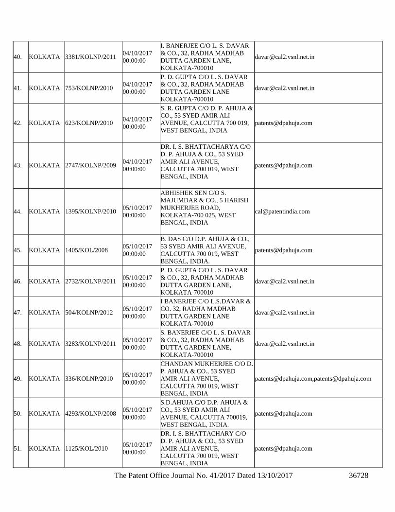
The Patent Office Journal No. 41/2017 Dated 13/10/2017 36728
40. KOLKATA 3381/KOLNP/2011 04/10/2017
00:00:00
I. BANERJEE C/O L. S. DAVAR
& CO., 32, RADHA MADHAB
DUTTA GARDEN LANE,
KOLKATA-700010
41. KOLKATA 753/KOLNP/2010 04/10/2017
00:00:00
P. D. GUPTA C/O L. S. DAVAR
& CO., 32, RADHA MADHAB
DUTTA GARDEN LANE
KOLKATA-700010
42. KOLKATA 623/KOLNP/2010 04/10/2017
00:00:00
S. R. GUPTA C/O D. P. AHUJA &
CO., 53 SYED AMIR ALI
AVENUE, CALCUTTA 700 019,
WEST BENGAL, INDIA
43. KOLKATA 2747/KOLNP/2009 04/10/2017
00:00:00
DR. I. S. BHATTACHARYA C/O
D. P. AHUJA & CO., 53 SYED
AMIR ALI AVENUE,
CALCUTTA 700 019, WEST
BENGAL, INDIA
44. KOLKATA 1395/KOLNP/2010 05/10/2017
00:00:00
ABHISHEK SEN C/O S.
MAJUMDAR & CO., 5 HARISH
MUKHERJEE ROAD,
KOLKATA-700 025, WEST
BENGAL, INDIA
45. KOLKATA 1405/KOL/2008 05/10/2017
00:00:00
B. DAS C/O D.P. AHUJA & CO.,
53 SYED AMIR ALI AVENUE,
CALCUTTA 700 019, WEST
BENGAL, INDIA.
46. KOLKATA 2732/KOLNP/2011 05/10/2017
00:00:00
P. D. GUPTA C/O L. S. DAVAR
& CO., 32, RADHA MADHAB
DUTTA GARDEN LANE,
KOLKATA-700010
47. KOLKATA 504/KOLNP/2012 05/10/2017
00:00:00
I BANERJEE C/O L.S.DAVAR &
CO. 32, RADHA MADHAB
DUTTA GARDEN LANE
KOLKATA-700010
48. KOLKATA 3283/KOLNP/2011 05/10/2017
00:00:00
S. BANERJEE C/O L. S. DAVAR
& CO., 32, RADHA MADHAB
DUTTA GARDEN LANE,
KOLKATA-700010
49. KOLKATA 336/KOLNP/2010 05/10/2017
00:00:00
CHANDAN MUKHERJEE C/O D.
P. AHUJA & CO., 53 SYED
AMIR ALI AVENUE,
CALCUTTA 700 019, WEST
BENGAL, INDIA
[email protected],[email protected]
50. KOLKATA 4293/KOLNP/2008 05/10/2017
00:00:00
S.D.AHUJA C/O D.P. AHUJA &
CO., 53 SYED AMIR ALI
AVENUE, CALCUTTA 700019,
WEST BENGAL, INDIA.
51. KOLKATA 1125/KOL/2010 05/10/2017
00:00:00
DR. I. S. BHATTACHARY C/O
D. P. AHUJA & CO., 53 SYED
AMIR ALI AVENUE,
CALCUTTA 700 019, WEST
BENGAL, INDIA
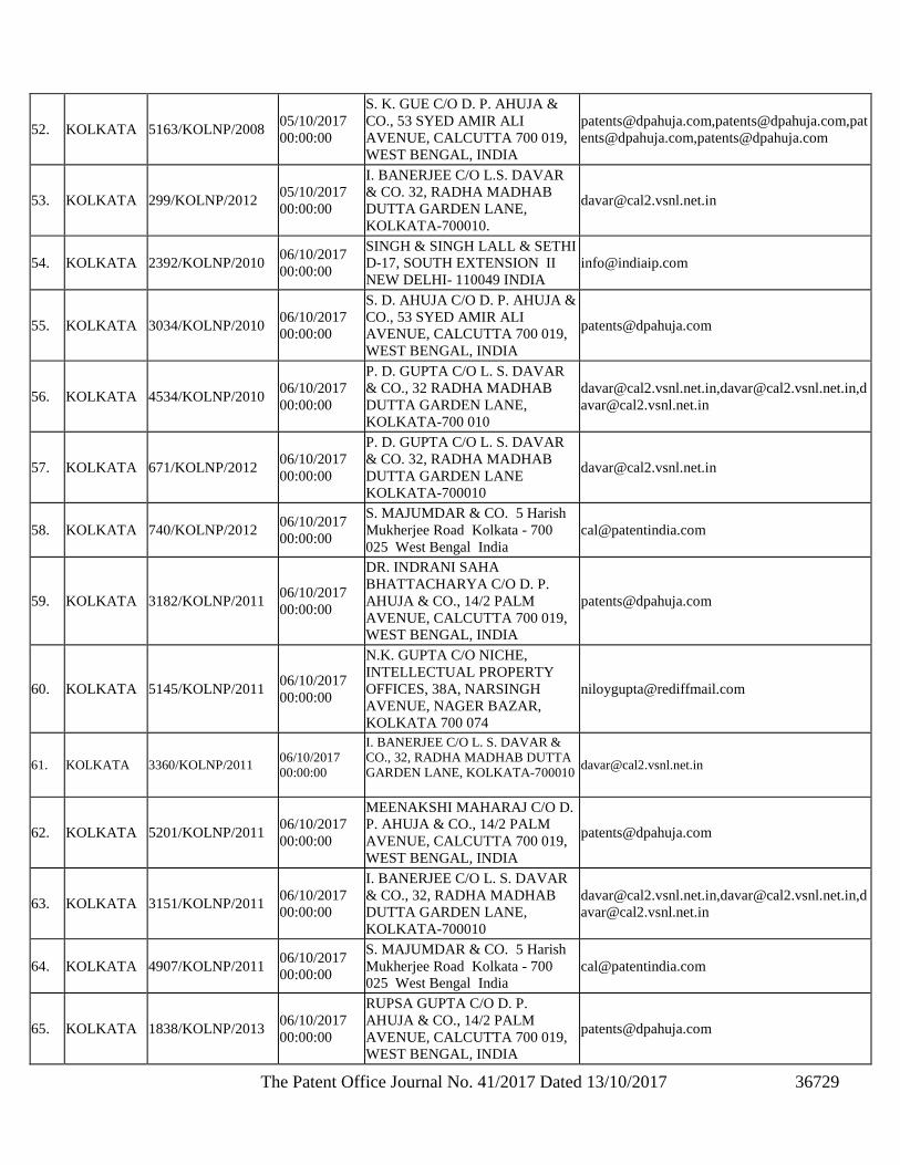
The Patent Office Journal No. 41/2017 Dated 13/10/2017 36729
52. KOLKATA 5163/KOLNP/2008 05/10/2017
00:00:00
S. K. GUE C/O D. P. AHUJA &
CO., 53 SYED AMIR ALI
AVENUE, CALCUTTA 700 019,
WEST BENGAL, INDIA
[email protected],[email protected],pat
[email protected],[email protected]
53. KOLKATA 299/KOLNP/2012 05/10/2017
00:00:00
I. BANERJEE C/O L.S. DAVAR
& CO. 32, RADHA MADHAB
DUTTA GARDEN LANE,
KOLKATA-700010.
54. KOLKATA 2392/KOLNP/2010 06/10/2017
00:00:00
SINGH & SINGH LALL & SETHI
D-17, SOUTH EXTENSION II
NEW DELHI- 110049 INDIA
55. KOLKATA 3034/KOLNP/2010 06/10/2017
00:00:00
S. D. AHUJA C/O D. P. AHUJA &
CO., 53 SYED AMIR ALI
AVENUE, CALCUTTA 700 019,
WEST BENGAL, INDIA
56. KOLKATA 4534/KOLNP/2010 06/10/2017
00:00:00
P. D. GUPTA C/O L. S. DAVAR
& CO., 32 RADHA MADHAB
DUTTA GARDEN LANE,
KOLKATA-700 010
[email protected],[email protected],d
57. KOLKATA 671/KOLNP/2012 06/10/2017
00:00:00
P. D. GUPTA C/O L. S. DAVAR
& CO. 32, RADHA MADHAB
DUTTA GARDEN LANE
KOLKATA-700010
58. KOLKATA 740/KOLNP/2012 06/10/2017
00:00:00
S. MAJUMDAR & CO. 5 Harish
Mukherjee Road Kolkata - 700
025 West Bengal India
59. KOLKATA 3182/KOLNP/2011 06/10/2017
00:00:00
DR. INDRANI SAHA
BHATTACHARYA C/O D. P.
AHUJA & CO., 14/2 PALM
AVENUE, CALCUTTA 700 019,
WEST BENGAL, INDIA
60. KOLKATA 5145/KOLNP/2011 06/10/2017
00:00:00
N.K. GUPTA C/O NICHE,
INTELLECTUAL PROPERTY
OFFICES, 38A, NARSINGH
AVENUE, NAGER BAZAR,
KOLKATA 700 074
61. KOLKATA 3360/KOLNP/2011 06/10/2017
00:00:00
I. BANERJEE C/O L. S. DAVAR &
CO., 32, RADHA MADHAB DUTTA
GARDEN LANE, KOLKATA-700010
62. KOLKATA 5201/KOLNP/2011 06/10/2017
00:00:00
MEENAKSHI MAHARAJ C/O D.
P. AHUJA & CO., 14/2 PALM
AVENUE, CALCUTTA 700 019,
WEST BENGAL, INDIA
63. KOLKATA 3151/KOLNP/2011 06/10/2017
00:00:00
I. BANERJEE C/O L. S. DAVAR
& CO., 32, RADHA MADHAB
DUTTA GARDEN LANE,
KOLKATA-700010
[email protected],[email protected],d
64. KOLKATA 4907/KOLNP/2011 06/10/2017
00:00:00
S. MAJUMDAR & CO. 5 Harish
Mukherjee Road Kolkata - 700
025 West Bengal India
65. KOLKATA 1838/KOLNP/2013 06/10/2017
00:00:00
RUPSA GUPTA C/O D. P.
AHUJA & CO., 14/2 PALM
AVENUE, CALCUTTA 700 019,
WEST BENGAL, INDIA
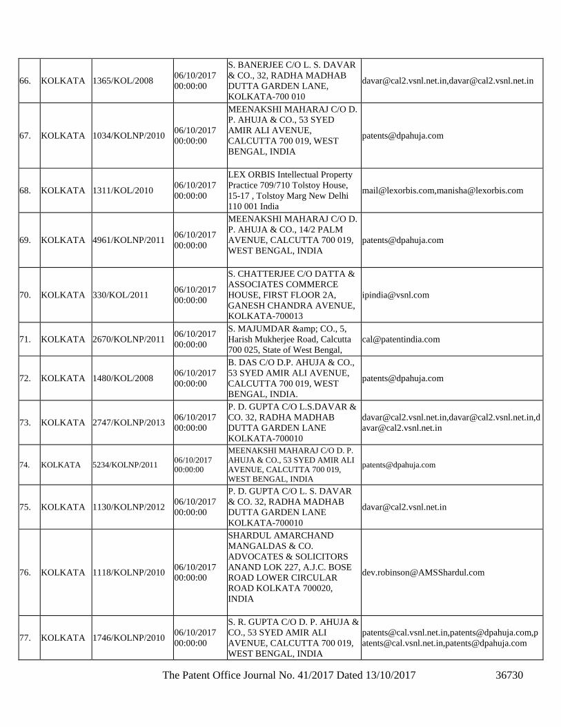
The Patent Office Journal No. 41/2017 Dated 13/10/2017 36730
66. KOLKATA 1365/KOL/2008 06/10/2017
00:00:00
S. BANERJEE C/O L. S. DAVAR
& CO., 32, RADHA MADHAB
DUTTA GARDEN LANE,
KOLKATA-700 010
[email protected],[email protected]
67. KOLKATA 1034/KOLNP/2010 06/10/2017
00:00:00
MEENAKSHI MAHARAJ C/O D.
P. AHUJA & CO., 53 SYED
AMIR ALI AVENUE,
CALCUTTA 700 019, WEST
BENGAL, INDIA
68. KOLKATA 1311/KOL/2010 06/10/2017
00:00:00
LEX ORBIS Intellectual Property
Practice 709/710 Tolstoy House,
15-17 , Tolstoy Marg New Delhi
110 001 India
[email protected],[email protected]
69. KOLKATA 4961/KOLNP/2011 06/10/2017
00:00:00
MEENAKSHI MAHARAJ C/O D.
P. AHUJA & CO., 14/2 PALM
AVENUE, CALCUTTA 700 019,
WEST BENGAL, INDIA
70. KOLKATA 330/KOL/2011 06/10/2017
00:00:00
S. CHATTERJEE C/O DATTA &
ASSOCIATES COMMERCE
HOUSE, FIRST FLOOR 2A,
GANESH CHANDRA AVENUE,
KOLKATA-700013
71. KOLKATA 2670/KOLNP/2011 06/10/2017
00:00:00
S. MAJUMDAR & CO., 5,
Harish Mukherjee Road, Calcutta
700 025, State of West Bengal,
72. KOLKATA 1480/KOL/2008 06/10/2017
00:00:00
B. DAS C/O D.P. AHUJA & CO.,
53 SYED AMIR ALI AVENUE,
CALCUTTA 700 019, WEST
BENGAL, INDIA.
73. KOLKATA 2747/KOLNP/2013 06/10/2017
00:00:00
P. D. GUPTA C/O L.S.DAVAR &
CO. 32, RADHA MADHAB
DUTTA GARDEN LANE
KOLKATA-700010
[email protected],[email protected],d
74. KOLKATA 5234/KOLNP/2011 06/10/2017
00:00:00
MEENAKSHI MAHARAJ C/O D. P.
AHUJA & CO., 53 SYED AMIR ALI
AVENUE, CALCUTTA 700 019,
WEST BENGAL, INDIA
75. KOLKATA 1130/KOLNP/2012 06/10/2017
00:00:00
P. D. GUPTA C/O L. S. DAVAR
& CO. 32, RADHA MADHAB
DUTTA GARDEN LANE
KOLKATA-700010
76. KOLKATA 1118/KOLNP/2010 06/10/2017
00:00:00
SHARDUL AMARCHAND
MANGALDAS & CO.
ADVOCATES & SOLICITORS
ANAND LOK 227, A.J.C. BOSE
ROAD LOWER CIRCULAR
ROAD KOLKATA 700020,
INDIA
77. KOLKATA 1746/KOLNP/2010 06/10/2017
00:00:00
S. R. GUPTA C/O D. P. AHUJA &
CO., 53 SYED AMIR ALI
AVENUE, CALCUTTA 700 019,
WEST BENGAL, INDIA
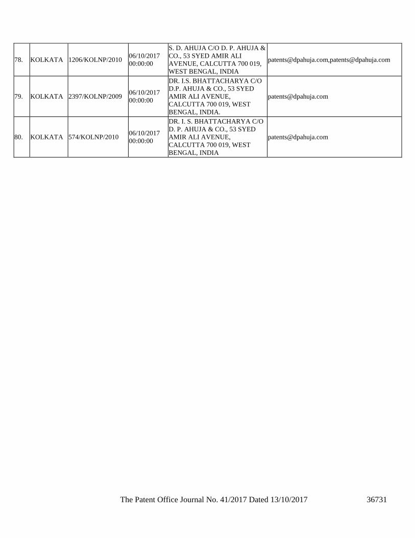
The Patent Office Journal No. 41/2017 Dated 13/10/2017 36731
78. KOLKATA 1206/KOLNP/2010 06/10/2017
00:00:00
S. D. AHUJA C/O D. P. AHUJA &
CO., 53 SYED AMIR ALI
AVENUE, CALCUTTA 700 019,
WEST BENGAL, INDIA
[email protected],[email protected]
79. KOLKATA 2397/KOLNP/2009 06/10/2017
00:00:00
DR. I.S. BHATTACHARYA C/O
D.P. AHUJA & CO., 53 SYED
AMIR ALI AVENUE,
CALCUTTA 700 019, WEST
BENGAL, INDIA.
80. KOLKATA 574/KOLNP/2010 06/10/2017
00:00:00
DR. I. S. BHATTACHARYA C/O
D. P. AHUJA & CO., 53 SYED
AMIR ALI AVENUE,
CALCUTTA 700 019, WEST
BENGAL, INDIA
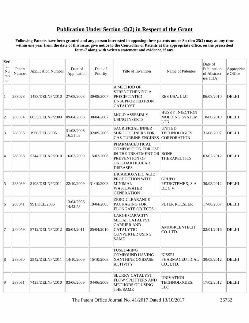
The Patent Office Journal No. 41/2017 Dated 13/10/2017 36732
Publication Under Section 43(2) in Respect of the Grant
Following Patents have been granted and any person interested in opposing these patents under Section 25(2) may at any time
within one year from the date of this issue, give notice to the Controller of Patents at the appropriate office, on the prescribed
form-7 along with written statement and evidence, if any.
Seri
al
Nu
mb
er
Patent
Number Application Number
Date of
Application
Date of
Priority Title of Invention Name of Patentee
Date of
Publication
of Abstract
u/s 11(A)
Appropriat
e Office
1 288028 1483/DELNP/2010 27/08/2008 30/08/2007
A METHOD OF
STRENGTHENING A
PRECIPITATED
UNSUPPORTED IRON
CATALYST
RES USA, LLC 06/08/2010 DELHI
2 288034 6655/DELNP/2009 09/04/2008 30/04/2007 MOLD ASSEMBLY
USING INSERTS
HUSKY INJECTION
MOLDING SYSTEM
LTD.
18/06/2010 DELHI
3 288035 1960/DEL/2006 31/08/2006
16:51:53 02/09/2005
SACRIFICIAL INNER
SHROUD LINERS FOR
GAS TURBINE ENGINES
UNITED
TECHNOLOGIES
CORPORATION
31/08/2007 DELHI
4 288038 5744/DELNP/2010 16/02/2009 15/02/2008
PHARMACEUTICAL
COMPOSITION FOR USE
IN THE TREATMENT OR
PREVENTION OF
OSTEOARTICULAR
DISEASES
BONE
THERAPEUTICS 03/02/2012 DELHI
5 288039 3108/DELNP/2011 22/10/2009 31/10/2008
DICARBOXYLIC ACID
PRODUCTION WITH
MINIMAL
WASTEWATER
GENERATION
GRUPO
PETROTEMEX, S.A.
DE C.V.
30/03/2012 DELHI
6 288041 991/DEL/2006 13/04/2006
14:42:53 19/04/2005
ZERO-CLEARANCE
PACKAGING FOR
ELONGATE OBJECTS
PETER ROESLER 17/08/2007 DELHI
7 288059 8712/DELNP/2012 05/04/2011 05/04/2010
LARGE CAPACITY
METAL CATALYST
CARRIER AND
CATALYTIC
CONVERTER USING
SAME
AMOGREENTECH
CO. LTD. 22/01/2016 DELHI
8 288060 2542/DELNP/2011 14/10/2009 15/10/2008
FUSED-RING
COMPOUND HAVING
XANTHINE OXIDASE
ACTIVITY
KISSEI
PHARMACEUTICAL
CO., LTD.
30/03/2012 DELHI
9 288061 7425/DELNP/2010 03/06/2009 04/06/2008
SLURRY CATALYST
FLOW SPLITTERS AND
METHODS OF USING
THE SAME
UNIVATION
TECHNOLOGIES,
LLC
17/02/2012 DELHI
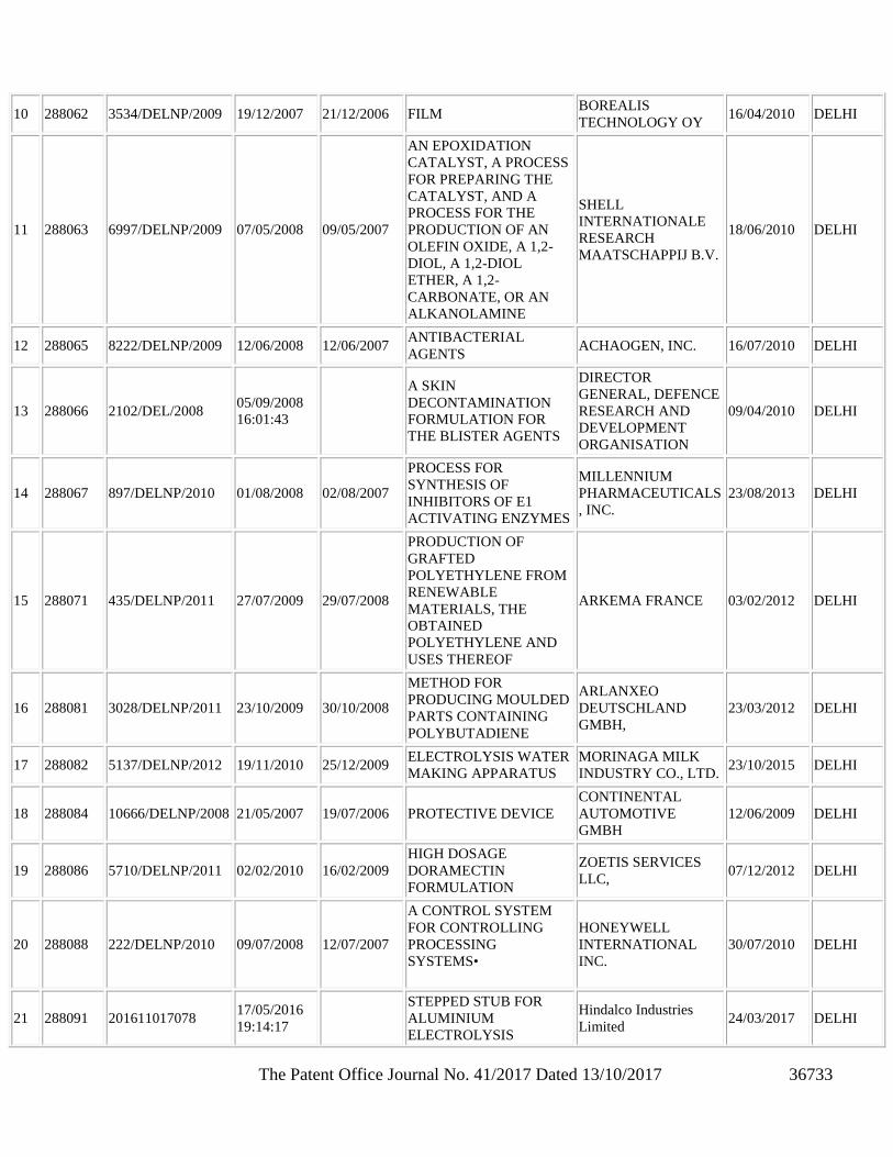
The Patent Office Journal No. 41/2017 Dated 13/10/2017 36733
10 288062 3534/DELNP/2009 19/12/2007 21/12/2006 FILM BOREALIS
TECHNOLOGY OY 16/04/2010 DELHI
11 288063 6997/DELNP/2009 07/05/2008 09/05/2007
AN EPOXIDATION
CATALYST, A PROCESS
FOR PREPARING THE
CATALYST, AND A
PROCESS FOR THE
PRODUCTION OF AN
OLEFIN OXIDE, A 1,2-
DIOL, A 1,2-DIOL
ETHER, A 1,2-
CARBONATE, OR AN
ALKANOLAMINE
SHELL
INTERNATIONALE
RESEARCH
MAATSCHAPPIJ B.V.
18/06/2010 DELHI
12 288065 8222/DELNP/2009 12/06/2008 12/06/2007 ANTIBACTERIAL
AGENTS ACHAOGEN, INC. 16/07/2010 DELHI
13 288066 2102/DEL/2008 05/09/2008
16:01:43
A SKIN
DECONTAMINATION
FORMULATION FOR
THE BLISTER AGENTS
DIRECTOR
GENERAL, DEFENCE
RESEARCH AND
DEVELOPMENT
ORGANISATION
09/04/2010 DELHI
14 288067 897/DELNP/2010 01/08/2008 02/08/2007
PROCESS FOR
SYNTHESIS OF
INHIBITORS OF E1
ACTIVATING ENZYMES
MILLENNIUM
PHARMACEUTICALS
, INC.
23/08/2013 DELHI
15 288071 435/DELNP/2011 27/07/2009 29/07/2008
PRODUCTION OF
GRAFTED
POLYETHYLENE FROM
RENEWABLE
MATERIALS, THE
OBTAINED
POLYETHYLENE AND
USES THEREOF
ARKEMA FRANCE 03/02/2012 DELHI
16 288081 3028/DELNP/2011 23/10/2009 30/10/2008
METHOD FOR
PRODUCING MOULDED
PARTS CONTAINING
POLYBUTADIENE
ARLANXEO
DEUTSCHLAND
GMBH,
23/03/2012 DELHI
17 288082 5137/DELNP/2012 19/11/2010 25/12/2009 ELECTROLYSIS WATER
MAKING APPARATUS
MORINAGA MILK
INDUSTRY CO., LTD. 23/10/2015 DELHI
18 288084 10666/DELNP/2008 21/05/2007 19/07/2006 PROTECTIVE DEVICE
CONTINENTAL
AUTOMOTIVE
GMBH
12/06/2009 DELHI
19 288086 5710/DELNP/2011 02/02/2010 16/02/2009
HIGH DOSAGE
DORAMECTIN
FORMULATION
ZOETIS SERVICES
LLC, 07/12/2012 DELHI
20 288088 222/DELNP/2010 09/07/2008 12/07/2007
A CONTROL SYSTEM
FOR CONTROLLING
PROCESSING
SYSTEMS•
HONEYWELL
INTERNATIONAL
INC.
30/07/2010 DELHI
21 288091 201611017078 17/05/2016
19:14:17
STEPPED STUB FOR
ALUMINIUM
ELECTROLYSIS
Hindalco Industries
Limited 24/03/2017 DELHI
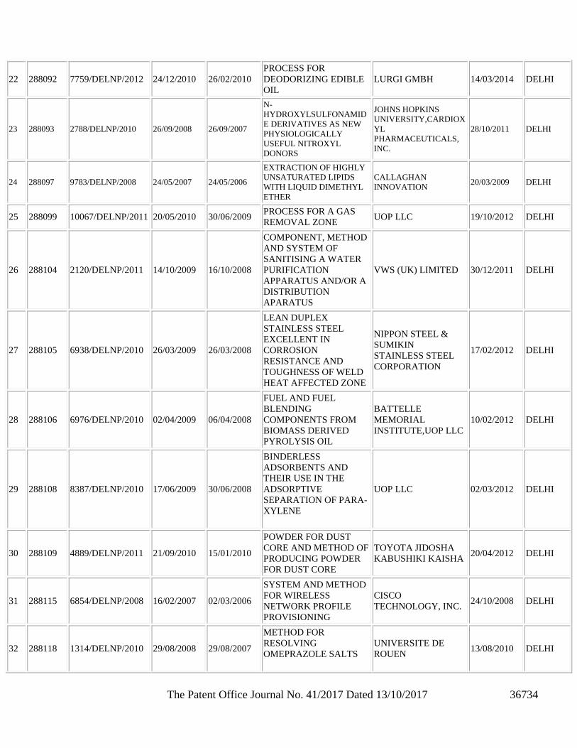
The Patent Office Journal No. 41/2017 Dated 13/10/2017 36734
22 288092 7759/DELNP/2012 24/12/2010 26/02/2010
PROCESS FOR
DEODORIZING EDIBLE
OIL
LURGI GMBH 14/03/2014 DELHI
23 288093 2788/DELNP/2010 26/09/2008 26/09/2007
N-
HYDROXYLSULFONAMID
E DERIVATIVES AS NEW
PHYSIOLOGICALLY
USEFUL NITROXYL
DONORS
JOHNS HOPKINS
UNIVERSITY,CARDIOX
YL
PHARMACEUTICALS,
INC.
28/10/2011 DELHI
24 288097 9783/DELNP/2008 24/05/2007 24/05/2006
EXTRACTION OF HIGHLY
UNSATURATED LIPIDS
WITH LIQUID DIMETHYL
ETHER
CALLAGHAN
INNOVATION 20/03/2009 DELHI
25 288099 10067/DELNP/2011 20/05/2010 30/06/2009 PROCESS FOR A GAS
REMOVAL ZONE UOP LLC 19/10/2012 DELHI
26 288104 2120/DELNP/2011 14/10/2009 16/10/2008
COMPONENT, METHOD
AND SYSTEM OF
SANITISING A WATER
PURIFICATION
APPARATUS AND/OR A
DISTRIBUTION
APARATUS
VWS (UK) LIMITED 30/12/2011 DELHI
27 288105 6938/DELNP/2010 26/03/2009 26/03/2008
LEAN DUPLEX
STAINLESS STEEL
EXCELLENT IN
CORROSION
RESISTANCE AND
TOUGHNESS OF WELD
HEAT AFFECTED ZONE
NIPPON STEEL &
SUMIKIN
STAINLESS STEEL
CORPORATION
17/02/2012 DELHI
28 288106 6976/DELNP/2010 02/04/2009 06/04/2008
FUEL AND FUEL
BLENDING
COMPONENTS FROM
BIOMASS DERIVED
PYROLYSIS OIL
BATTELLE
MEMORIAL
INSTITUTE,UOP LLC
10/02/2012 DELHI
29 288108 8387/DELNP/2010 17/06/2009 30/06/2008
BINDERLESS
ADSORBENTS AND
THEIR USE IN THE
ADSORPTIVE
SEPARATION OF PARA-
XYLENE
UOP LLC 02/03/2012 DELHI
30 288109 4889/DELNP/2011 21/09/2010 15/01/2010
POWDER FOR DUST
CORE AND METHOD OF
PRODUCING POWDER
FOR DUST CORE
TOYOTA JIDOSHA
KABUSHIKI KAISHA 20/04/2012 DELHI
31 288115 6854/DELNP/2008 16/02/2007 02/03/2006
SYSTEM AND METHOD
FOR WIRELESS
NETWORK PROFILE
PROVISIONING
CISCO
TECHNOLOGY, INC. 24/10/2008 DELHI
32 288118 1314/DELNP/2010 29/08/2008 29/08/2007
METHOD FOR
RESOLVING
OMEPRAZOLE SALTS
UNIVERSITE DE
ROUEN 13/08/2010 DELHI
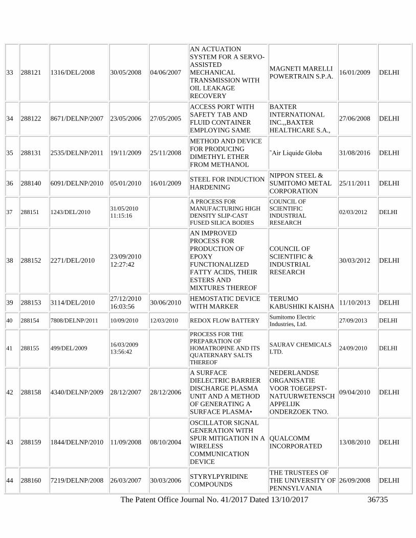
The Patent Office Journal No. 41/2017 Dated 13/10/2017 36735
33 288121 1316/DEL/2008 30/05/2008 04/06/2007
AN ACTUATION
SYSTEM FOR A SERVO-
ASSISTED
MECHANICAL
TRANSMISSION WITH
OIL LEAKAGE
RECOVERY
MAGNETI MARELLI
POWERTRAIN S.P.A. 16/01/2009 DELHI
34 288122 8671/DELNP/2007 23/05/2006 27/05/2005
ACCESS PORT WITH
SAFETY TAB AND
FLUID CONTAINER
EMPLOYING SAME
BAXTER
INTERNATIONAL
INC.,,BAXTER
HEALTHCARE S.A.,
27/06/2008 DELHI
35 288131 2535/DELNP/2011 19/11/2009 25/11/2008
METHOD AND DEVICE
FOR PRODUCING
DIMETHYL ETHER
FROM METHANOL
˜Air Liquide Globa 31/08/2016 DELHI
36 288140 6091/DELNP/2010 05/01/2010 16/01/2009 STEEL FOR INDUCTION
HARDENING
NIPPON STEEL &
SUMITOMO METAL
CORPORATION
25/11/2011 DELHI
37 288151 1243/DEL/2010 31/05/2010
11:15:16
A PROCESS FOR
MANUFACTURING HIGH
DENSITY SLIP-CAST
FUSED SILICA BODIES
COUNCIL OF
SCIENTIFIC
INDUSTRIAL
RESEARCH
02/03/2012 DELHI
38 288152 2271/DEL/2010 23/09/2010
12:27:42
AN IMPROVED
PROCESS FOR
PRODUCTION OF
EPOXY
FUNCTIONALIZED
FATTY ACIDS, THEIR
ESTERS AND
MIXTURES THEREOF
COUNCIL OF
SCIENTIFIC &
INDUSTRIAL
RESEARCH
30/03/2012 DELHI
39 288153 3114/DEL/2010 27/12/2010
16:03:56 30/06/2010
HEMOSTATIC DEVICE
WITH MARKER
TERUMO
KABUSHIKI KAISHA 11/10/2013 DELHI
40 288154 7808/DELNP/2011 10/09/2010 12/03/2010 REDOX FLOW BATTERY Sumitomo Electric
Industries, Ltd. 27/09/2013 DELHI
41 288155 499/DEL/2009 16/03/2009
13:56:42
PROCESS FOR THE
PREPARATION OF
HOMATROPINE AND ITS
QUATERNARY SALTS
THEREOF
SAURAV CHEMICALS
LTD. 24/09/2010 DELHI
42 288158 4340/DELNP/2009 28/12/2007 28/12/2006
A SURFACE
DIELECTRIC BARRIER
DISCHARGE PLASMA
UNIT AND A METHOD
OF GENERATING A
SURFACE PLASMA•
NEDERLANDSE
ORGANISATIE
VOOR TOEGEPST-
NATUURWETENSCH
APPELIJK
ONDERZOEK TNO.
09/04/2010 DELHI
43 288159 1844/DELNP/2010 11/09/2008 08/10/2004
OSCILLATOR SIGNAL
GENERATION WITH
SPUR MITIGATION IN A
WIRELESS
COMMUNICATION
DEVICE
QUALCOMM
INCORPORATED 13/08/2010 DELHI
44 288160 7219/DELNP/2008 26/03/2007 30/03/2006 STYRYLPYRIDINE
COMPOUNDS
THE TRUSTEES OF
THE UNIVERSITY OF
PENNSYLVANIA
26/09/2008 DELHI
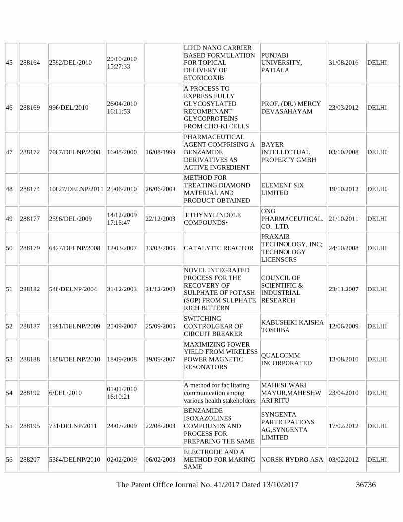
The Patent Office Journal No. 41/2017 Dated 13/10/2017 36736
45 288164 2592/DEL/2010 29/10/2010
15:27:33
LIPID NANO CARRIER
BASED FORMULATION
FOR TOPICAL
DELIVERY OF
ETORICOXIB
PUNJABI
UNIVERSITY,
PATIALA
31/08/2016 DELHI
46 288169 996/DEL/2010 26/04/2010
16:11:53
A PROCESS TO
EXPRESS FULLY
GLYCOSYLATED
RECOMBINANT
GLYCOPROTEINS
FROM CHO-KI CELLS
PROF. (DR.) MERCY
DEVASAHAYAM 23/03/2012 DELHI
47 288172 7087/DELNP/2008 16/08/2000 16/08/1999
PHARMACEUTICAL
AGENT COMPRISING A
BENZAMIDE
DERIVATIVES AS
ACTIVE INGREDIENT
BAYER
INTELLECTUAL
PROPERTY GMBH
03/10/2008 DELHI
48 288174 10027/DELNP/2011 25/06/2010 26/06/2009
METHOD FOR
TREATING DIAMOND
MATERIAL AND
PRODUCT OBTAINED
ELEMENT SIX
LIMITED 19/10/2012 DELHI
49 288177 2596/DEL/2009 14/12/2009
17:16:47 22/12/2008
ETHYNYLINDOLE
COMPOUNDS•
ONO
PHARMACEUTICAL.
CO. LTD.
21/10/2011 DELHI
50 288179 6427/DELNP/2008 12/03/2007 13/03/2006 CATALYTIC REACTOR
PRAXAIR
TECHNOLOGY, INC;
TECHNOLOGY
LICENSORS
24/10/2008 DELHI
51 288182 548/DELNP/2004 31/12/2003 31/12/2003
NOVEL INTEGRATED
PROCESS FOR THE
RECOVERY OF
SULPHATE OF POTASH
(SOP) FROM SULPHATE
RICH BITTERN
COUNCIL OF
SCIENTIFIC &
INDUSTRIAL
RESEARCH
23/11/2007 DELHI
52 288187 1991/DELNP/2009 25/09/2007 25/09/2006
SWITCHING
CONTROLGEAR OF
CIRCUIT BREAKER
KABUSHIKI KAISHA
TOSHIBA 12/06/2009 DELHI
53 288188 1858/DELNP/2010 18/09/2008 19/09/2007
MAXIMIZING POWER
YIELD FROM WIRELESS
POWER MAGNETIC
RESONATORS
QUALCOMM
INCORPORATED 13/08/2010 DELHI
54 288192 6/DEL/2010 01/01/2010
16:10:21
A method for facilitating
communication among
various health stakeholders
MAHESHWARI
MAYUR,MAHESHW
ARI RITU
23/04/2010 DELHI
55 288195 731/DELNP/2011 24/07/2009 22/08/2008
BENZAMIDE
ISOXAZOLINES
COMPOUNDS AND
PROCESS FOR
PREPARING THE SAME
SYNGENTA
PARTICIPATIONS
AG,SYNGENTA
LIMITED
17/02/2012 DELHI
56 288207 5384/DELNP/2010 02/02/2009 06/02/2008
ELECTRODE AND A
METHOD FOR MAKING
SAME
NORSK HYDRO ASA 03/02/2012 DELHI
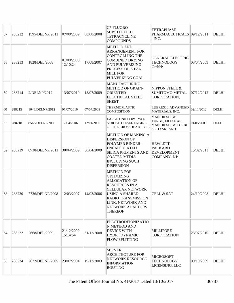
The Patent Office Journal No. 41/2017 Dated 13/10/2017 36737
57 288212 1595/DELNP/2011 07/08/2009 08/08/2008
C7-FLUORO
SUBSTITUTED
TETRACYCLINE
COMPOUNDS
TETRAPHASE
PHARMACEUTICALS
, INC.
09/12/2011 DELHI
58 288213 1828/DEL/2008 01/08/2008
12:10:24 17/08/2007
METHOD AND
ARRANGEMENT FOR
CONTROLLING THE
COMBINED DRYING
AND PULVERIZING
PROCESS OF A FAN
MILL FOR
PULVERIZING COAL
GENERAL ELECTRIC
TECHNOLOGY
GmbH•
03/04/2009 DELHI
59 288214 2/DELNP/2012 13/07/2010 13/07/2009
MANUFACTURING
METHOD OF GRAIN-
ORIENTED
ELECTRICAL STEEL
SHEET
NIPPON STEEL &
SUMITOMO METAL
CORPORATION,
07/12/2012 DELHI
60 288215 1048/DELNP/2012 07/07/2010 07/07/2009 THERMOPLASTIC
COMPOSITION
LUBRIZOL ADVANCED
MATERIALS, INC. 02/11/2012 DELHI
61 288218 8563/DELNP/2008 12/04/2006 12/04/2006
LARGE UNIFLOW TWO-
STROKE DIESEL ENGINE
OF THE CROSSHEAD TYPE
MAN DIESEL &
TURBO, FILIAL AF
MAN DIESEL & TURBO
SE, TYSKLAND
01/05/2009 DELHI
62 288219 8938/DELNP/2011 30/04/2009 30/04/2009
METHOD OF MAKING A
DISPERSION OF
POLYMER BINDER-
ENCAPSULATED
SILICA PIGMENTS AND
COATED MEDIA
INCLUDING SUCH
DISPERSION
HEWLETT-
PACKARD
DEVELOPMENT
COMPANY, L.P.
15/02/2013 DELHI
63 288220 7726/DELNP/2008 12/03/2007 14/03/2006
METHOD FOR
OPTIMIZING
ALLOCATION OF
RESOURCES IN A
CELLULAR NETWORK
USING A SHARED
RADIO TRANSMISSION
LINK, NETWORK AND
NETWORK ADAPTORS
THEREOF
CELL & SAT 24/10/2008 DELHI
64 288222 2668/DEL/2009 21/12/2009
15:14:54 31/12/2008
ELECTRODEIONIZATIO
N METHOD AND
DEVICE WITH
HYDRODYNAMIC
FLOW SPLITTING
MILLIPORE
CORPORATION 23/07/2010 DELHI
65 288224 2672/DELNP/2005 23/07/2004 19/12/2003
SERVER
ARCHITECTURE FOR
NETWORK RESOURCE
INFORMATION
ROUTING
MICROSOFT
TECHNOLOGY
LICENSING, LLC
09/10/2009 DELHI
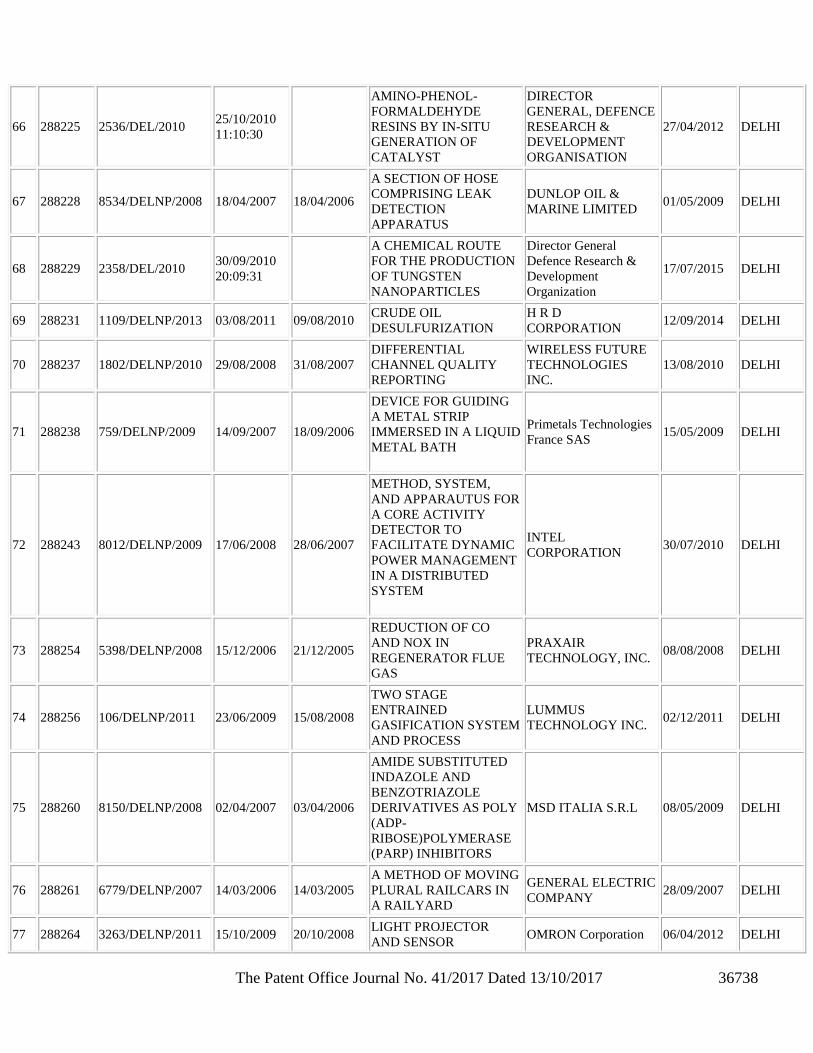
The Patent Office Journal No. 41/2017 Dated 13/10/2017 36738
66 288225 2536/DEL/2010 25/10/2010
11:10:30
AMINO-PHENOL-
FORMALDEHYDE
RESINS BY IN-SITU
GENERATION OF
CATALYST
DIRECTOR
GENERAL, DEFENCE
RESEARCH &
DEVELOPMENT
ORGANISATION
27/04/2012 DELHI
67 288228 8534/DELNP/2008 18/04/2007 18/04/2006
A SECTION OF HOSE
COMPRISING LEAK
DETECTION
APPARATUS
DUNLOP OIL &
MARINE LIMITED 01/05/2009 DELHI
68 288229 2358/DEL/2010 30/09/2010
20:09:31
A CHEMICAL ROUTE
FOR THE PRODUCTION
OF TUNGSTEN
NANOPARTICLES
Director General
Defence Research &
Development
Organization
17/07/2015 DELHI
69 288231 1109/DELNP/2013 03/08/2011 09/08/2010 CRUDE OIL
DESULFURIZATION
H R D
CORPORATION 12/09/2014 DELHI
70 288237 1802/DELNP/2010 29/08/2008 31/08/2007
DIFFERENTIAL
CHANNEL QUALITY
REPORTING
WIRELESS FUTURE
TECHNOLOGIES
INC.
13/08/2010 DELHI
71 288238 759/DELNP/2009 14/09/2007 18/09/2006
DEVICE FOR GUIDING
A METAL STRIP
IMMERSED IN A LIQUID
METAL BATH
Primetals Technologies
France SAS 15/05/2009 DELHI
72 288243 8012/DELNP/2009 17/06/2008 28/06/2007
METHOD, SYSTEM,
AND APPARAUTUS FOR
A CORE ACTIVITY
DETECTOR TO
FACILITATE DYNAMIC
POWER MANAGEMENT
IN A DISTRIBUTED
SYSTEM
INTEL
CORPORATION 30/07/2010 DELHI
73 288254 5398/DELNP/2008 15/12/2006 21/12/2005
REDUCTION OF CO
AND NOX IN
REGENERATOR FLUE
GAS
PRAXAIR
TECHNOLOGY, INC. 08/08/2008 DELHI
74 288256 106/DELNP/2011 23/06/2009 15/08/2008
TWO STAGE
ENTRAINED
GASIFICATION SYSTEM
AND PROCESS
LUMMUS
TECHNOLOGY INC. 02/12/2011 DELHI
75 288260 8150/DELNP/2008 02/04/2007 03/04/2006
AMIDE SUBSTITUTED
INDAZOLE AND
BENZOTRIAZOLE
DERIVATIVES AS POLY
(ADP-
RIBOSE)POLYMERASE
(PARP) INHIBITORS
MSD ITALIA S.R.L 08/05/2009 DELHI
76 288261 6779/DELNP/2007 14/03/2006 14/03/2005
A METHOD OF MOVING
PLURAL RAILCARS IN
A RAILYARD
GENERAL ELECTRIC
COMPANY 28/09/2007 DELHI
77 288264 3263/DELNP/2011 15/10/2009 20/10/2008 LIGHT PROJECTOR
AND SENSOR OMRON Corporation 06/04/2012 DELHI
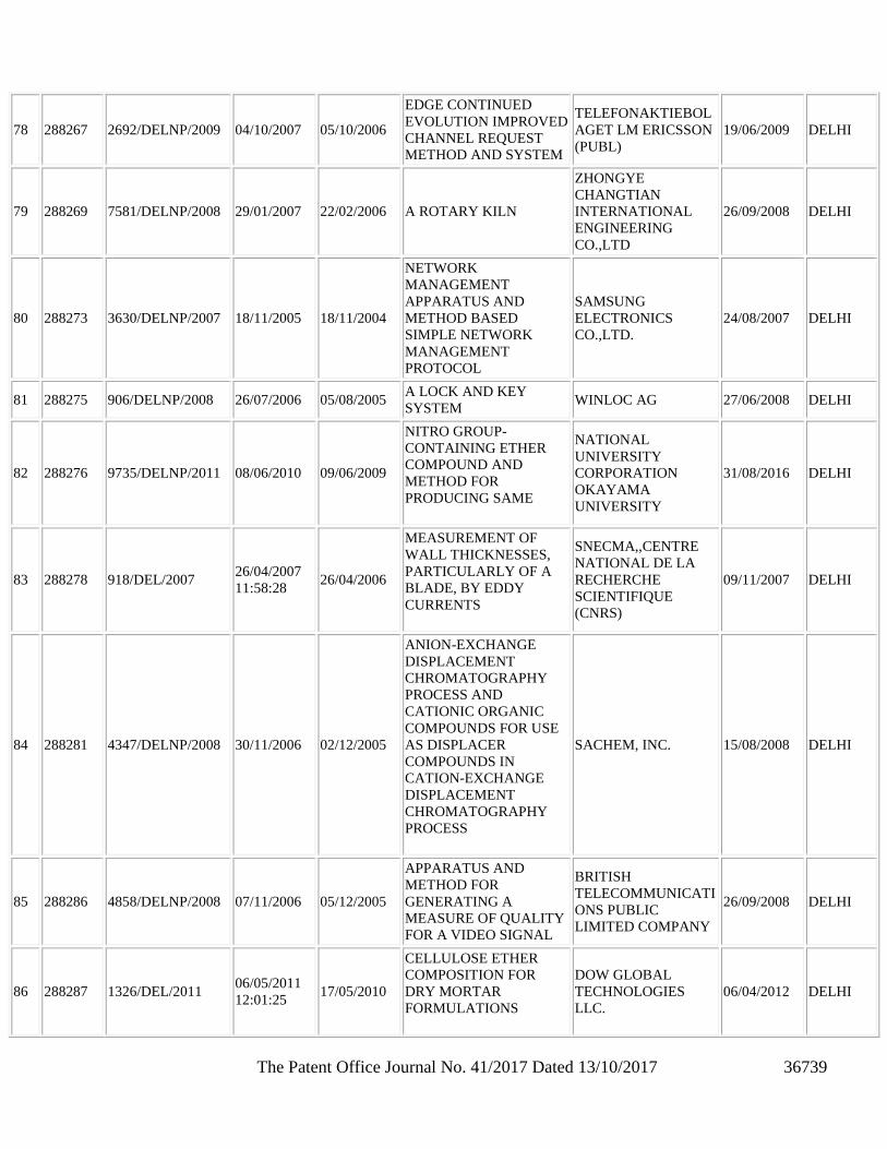
The Patent Office Journal No. 41/2017 Dated 13/10/2017 36739
78 288267 2692/DELNP/2009 04/10/2007 05/10/2006
EDGE CONTINUED
EVOLUTION IMPROVED
CHANNEL REQUEST
METHOD AND SYSTEM
TELEFONAKTIEBOL
AGET LM ERICSSON
(PUBL)
19/06/2009 DELHI
79 288269 7581/DELNP/2008 29/01/2007 22/02/2006 A ROTARY KILN
ZHONGYE
CHANGTIAN
INTERNATIONAL
ENGINEERING
CO.,LTD
26/09/2008 DELHI
80 288273 3630/DELNP/2007 18/11/2005 18/11/2004
NETWORK
MANAGEMENT
APPARATUS AND
METHOD BASED
SIMPLE NETWORK
MANAGEMENT
PROTOCOL
SAMSUNG
ELECTRONICS
CO.,LTD.
24/08/2007 DELHI
81 288275 906/DELNP/2008 26/07/2006 05/08/2005 A LOCK AND KEY
SYSTEM WINLOC AG 27/06/2008 DELHI
82 288276 9735/DELNP/2011 08/06/2010 09/06/2009
NITRO GROUP-
CONTAINING ETHER
COMPOUND AND
METHOD FOR
PRODUCING SAME
NATIONAL
UNIVERSITY
CORPORATION
OKAYAMA
UNIVERSITY
31/08/2016 DELHI
83 288278 918/DEL/2007 26/04/2007
11:58:28 26/04/2006
MEASUREMENT OF
WALL THICKNESSES,
PARTICULARLY OF A
BLADE, BY EDDY
CURRENTS
SNECMA,,CENTRE
NATIONAL DE LA
RECHERCHE
SCIENTIFIQUE
(CNRS)
09/11/2007 DELHI
84 288281 4347/DELNP/2008 30/11/2006 02/12/2005
ANION-EXCHANGE
DISPLACEMENT
CHROMATOGRAPHY
PROCESS AND
CATIONIC ORGANIC
COMPOUNDS FOR USE
AS DISPLACER
COMPOUNDS IN
CATION-EXCHANGE
DISPLACEMENT
CHROMATOGRAPHY
PROCESS
SACHEM, INC. 15/08/2008 DELHI
85 288286 4858/DELNP/2008 07/11/2006 05/12/2005
APPARATUS AND
METHOD FOR
GENERATING A
MEASURE OF QUALITY
FOR A VIDEO SIGNAL
BRITISH
TELECOMMUNICATI
ONS PUBLIC
LIMITED COMPANY
26/09/2008 DELHI
86 288287 1326/DEL/2011 06/05/2011
12:01:25 17/05/2010
CELLULOSE ETHER
COMPOSITION FOR
DRY MORTAR
FORMULATIONS
DOW GLOBAL
TECHNOLOGIES
LLC.
06/04/2012 DELHI
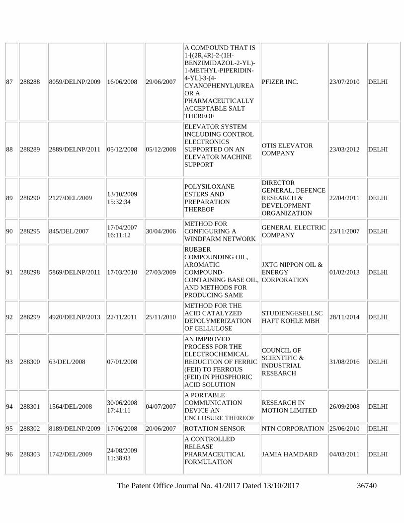
The Patent Office Journal No. 41/2017 Dated 13/10/2017 36740
87 288288 8059/DELNP/2009 16/06/2008 29/06/2007
A COMPOUND THAT IS
1-[(2R,4R)-2-(1H-
BENZIMIDAZOL-2-YL)-
1-METHYL-PIPERIDIN-
4-YL]-3-(4-
CYANOPHENYL)UREA
OR A
PHARMACEUTICALLY
ACCEPTABLE SALT
THEREOF
PFIZER INC. 23/07/2010 DELHI
88 288289 2889/DELNP/2011 05/12/2008 05/12/2008
ELEVATOR SYSTEM
INCLUDING CONTROL
ELECTRONICS
SUPPORTED ON AN
ELEVATOR MACHINE
SUPPORT
OTIS ELEVATOR
COMPANY 23/03/2012 DELHI
89 288290 2127/DEL/2009 13/10/2009
15:32:34
POLYSILOXANE
ESTERS AND
PREPARATION
THEREOF
DIRECTOR
GENERAL, DEFENCE
RESEARCH &
DEVELOPMENT
ORGANIZATION
22/04/2011 DELHI
90 288295 845/DEL/2007 17/04/2007
16:11:12 30/04/2006
METHOD FOR
CONFIGURING A
WINDFARM NETWORK
GENERAL ELECTRIC
COMPANY 23/11/2007 DELHI
91 288298 5869/DELNP/2011 17/03/2010 27/03/2009
RUBBER
COMPOUNDING OIL,
AROMATIC
COMPOUND-
CONTAINING BASE OIL,
AND METHODS FOR
PRODUCING SAME
JXTG NIPPON OIL &
ENERGY
CORPORATION
01/02/2013 DELHI
92 288299 4920/DELNP/2013 22/11/2011 25/11/2010
METHOD FOR THE
ACID CATALYZED
DEPOLYMERIZATION
OF CELLULOSE
STUDIENGESELLSC
HAFT KOHLE MBH 28/11/2014 DELHI
93 288300 63/DEL/2008 07/01/2008
AN IMPROVED
PROCESS FOR THE
ELECTROCHEMICAL
REDUCTION OF FERRIC
(FEII) TO FERROUS
(FEII) IN PHOSPHORIC
ACID SOLUTION
COUNCIL OF
SCIENTIFIC &
INDUSTRIAL
RESEARCH
31/08/2016 DELHI
94 288301 1564/DEL/2008 30/06/2008
17:41:11 04/07/2007
A PORTABLE
COMMUNICATION
DEVICE AN
ENCLOSURE THEREOF
RESEARCH IN
MOTION LIMITED 26/09/2008 DELHI
95 288302 8189/DELNP/2009 17/06/2008 20/06/2007 ROTATION SENSOR NTN CORPORATION 25/06/2010 DELHI
96 288303 1742/DEL/2009 24/08/2009
11:38:03
A CONTROLLED
RELEASE
PHARMACEUTICAL
FORMULATION
JAMIA HAMDARD 04/03/2011 DELHI
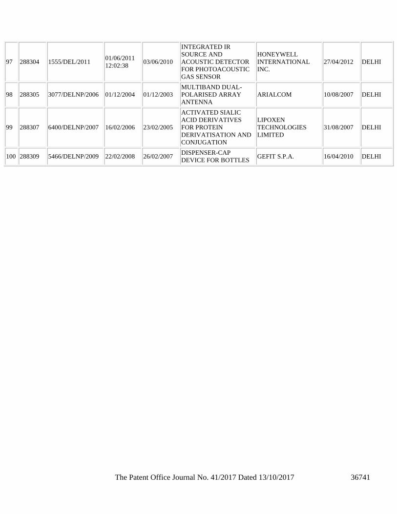
The Patent Office Journal No. 41/2017 Dated 13/10/2017 36741
97 288304 1555/DEL/2011 01/06/2011
12:02:38 03/06/2010
INTEGRATED IR
SOURCE AND
ACOUSTIC DETECTOR
FOR PHOTOACOUSTIC
GAS SENSOR
HONEYWELL
INTERNATIONAL
INC.
27/04/2012 DELHI
98 288305 3077/DELNP/2006 01/12/2004 01/12/2003
MULTIBAND DUAL-
POLARISED ARRAY
ANTENNA
ARIALCOM 10/08/2007 DELHI
99 288307 6400/DELNP/2007 16/02/2006 23/02/2005
ACTIVATED SIALIC
ACID DERIVATIVES
FOR PROTEIN
DERIVATISATION AND
CONJUGATION
LIPOXEN
TECHNOLOGIES
LIMITED
31/08/2007 DELHI
100 288309 5466/DELNP/2009 22/02/2008 26/02/2007 DISPENSER-CAP
DEVICE FOR BOTTLES GEFIT S.P.A. 16/04/2010 DELHI
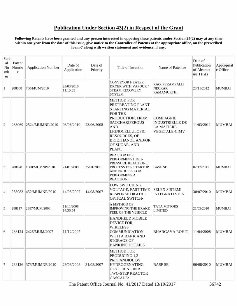
The Patent Office Journal No. 41/2017 Dated 13/10/2017 36742
Publication Under Section 43(2) in Respect of the Grant
Following Patents have been granted and any person interested in opposing these patents under Section 25(2) may at any time
within one year from the date of this issue, give notice to the Controller of Patents at the appropriate office, on the prescribed
form-7 along with written statement and evidence, if any.
Seri
al
Nu
mb
er
Patent
Numbe
r
Application Number Date of
Application
Date of
Priority Title of Invention Name of Patentee
Date of
Publication
of Abstract
u/s 11(A)
Appropriat
e Office
1 288068 780/MUM/2010 23/03/2010
11:15:35
CONVEYOR HEATER
DRYER WITH VAPOUR /
STEAM RECOVERY
SYSTEM
RAO, PERAMPALLI
NECKAR
RAMAMURTHI
23/11/2012 MUMBAI
2 288069 2524/MUMNP/2010 03/06/2010 23/06/2008
METHOD FOR
PRETREATING PLANT
STARTING MATERIAL
FOR THE
PRODUCTION, FROM
SACCHARIFEROUS
AND
LIGNOCELLULOSIC
RESOURCES, OF
BIOETHANOL AND/OR
OF SUGAR, AND
PLANT
COMPAGNIE
INDUSTRIELLE DE
LA MATIERE
VEGETALE-CIMV
11/03/2011 MUMBAI
3 288078 1580/MUMNP/2010 21/01/2009 25/01/2008
REACTOR FOR
PERFORMING HIGH-
PRESSURE REACTIONS,
PROCESS FOR STARTUP
AND PROCESS FOR
PERFORMING A
REACTION•
BASF SE 02/12/2011 MUMBAI
4 288083 452/MUMNP/2010 14/08/2007 14/08/2007
LOW SWITCHING
VOLTAGE, FAST TIME
RESPONSE DIGITAL
OPTICAL SWITCH•
SELEX SISTEMI
INTEGRATI S.P.A. 30/07/2010 MUMBAI
5 288117 2387/MUM/2008 11/11/2008
14:36:54
A METHOD OF
IMPROVING THE BRAKE
FEEL OF THE VEHICLE
TATA MOTORS
LIMITED 21/05/2010 MUMBAI
6 288124 2426/MUM/2007 11/12/2007
HANDHELD MOBILE
DEVICE FOR
WIRELESS
COMMUNICATION
WITH A BANK AND
STORAGE OF
BANKING DETAILS
BHARGAVA ROHIT 11/04/2008 MUMBAI
7 288126 373/MUMNP/2010 29/08/2008 31/08/2007
METHOD FOR
PRODUCING 1,2-
PROPANDIOL BY
HYDROGENATING
GLYCERINE IN A
TWO-STEP REACTOR
CASCADE•
BASF SE 06/08/2010 MUMBAI
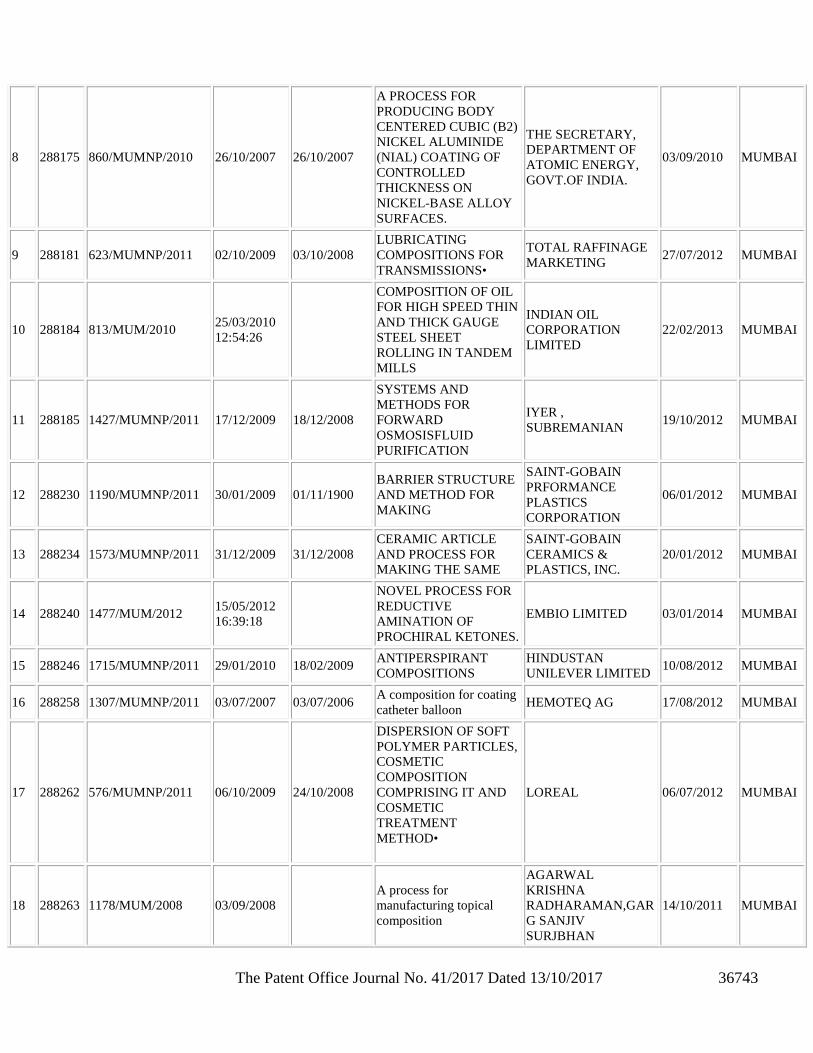
The Patent Office Journal No. 41/2017 Dated 13/10/2017 36743
8 288175 860/MUMNP/2010 26/10/2007 26/10/2007
A PROCESS FOR
PRODUCING BODY
CENTERED CUBIC (B2)
NICKEL ALUMINIDE
(NIAL) COATING OF
CONTROLLED
THICKNESS ON
NICKEL-BASE ALLOY
SURFACES.
THE SECRETARY,
DEPARTMENT OF
ATOMIC ENERGY,
GOVT.OF INDIA.
03/09/2010 MUMBAI
9 288181 623/MUMNP/2011 02/10/2009 03/10/2008
LUBRICATING
COMPOSITIONS FOR
TRANSMISSIONS•
TOTAL RAFFINAGE
MARKETING 27/07/2012 MUMBAI
10 288184 813/MUM/2010 25/03/2010
12:54:26
COMPOSITION OF OIL
FOR HIGH SPEED THIN
AND THICK GAUGE
STEEL SHEET
ROLLING IN TANDEM
MILLS
INDIAN OIL
CORPORATION
LIMITED
22/02/2013 MUMBAI
11 288185 1427/MUMNP/2011 17/12/2009 18/12/2008
SYSTEMS AND
METHODS FOR
FORWARD
OSMOSISFLUID
PURIFICATION
IYER ,
SUBREMANIAN 19/10/2012 MUMBAI
12 288230 1190/MUMNP/2011 30/01/2009 01/11/1900
BARRIER STRUCTURE
AND METHOD FOR
MAKING
SAINT-GOBAIN
PRFORMANCE
PLASTICS
CORPORATION
06/01/2012 MUMBAI
13 288234 1573/MUMNP/2011 31/12/2009 31/12/2008
CERAMIC ARTICLE
AND PROCESS FOR
MAKING THE SAME
SAINT-GOBAIN
CERAMICS &
PLASTICS, INC.
20/01/2012 MUMBAI
14 288240 1477/MUM/2012 15/05/2012
16:39:18
NOVEL PROCESS FOR
REDUCTIVE
AMINATION OF
PROCHIRAL KETONES.
EMBIO LIMITED 03/01/2014 MUMBAI
15 288246 1715/MUMNP/2011 29/01/2010 18/02/2009 ANTIPERSPIRANT
COMPOSITIONS
HINDUSTAN
UNILEVER LIMITED 10/08/2012 MUMBAI
16 288258 1307/MUMNP/2011 03/07/2007 03/07/2006 A composition for coating
catheter balloon HEMOTEQ AG 17/08/2012 MUMBAI
17 288262 576/MUMNP/2011 06/10/2009 24/10/2008
DISPERSION OF SOFT
POLYMER PARTICLES,
COSMETIC
COMPOSITION
COMPRISING IT AND
COSMETIC
TREATMENT
METHOD•
LOREAL 06/07/2012 MUMBAI
18 288263 1178/MUM/2008 03/09/2008
A process for
manufacturing topical
composition
AGARWAL
KRISHNA
RADHARAMAN,GAR
G SANJIV
SURJBHAN
14/10/2011 MUMBAI
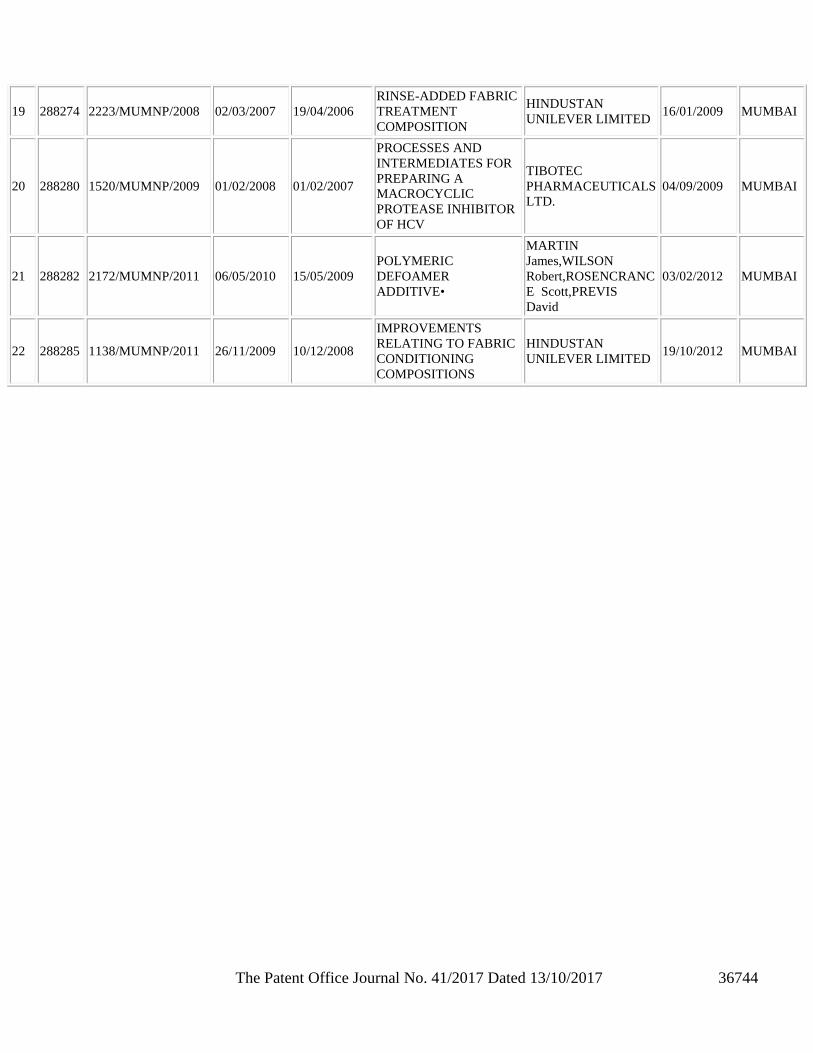
The Patent Office Journal No. 41/2017 Dated 13/10/2017 36744
19 288274 2223/MUMNP/2008 02/03/2007 19/04/2006
RINSE-ADDED FABRIC
TREATMENT
COMPOSITION
HINDUSTAN
UNILEVER LIMITED 16/01/2009 MUMBAI
20 288280 1520/MUMNP/2009 01/02/2008 01/02/2007
PROCESSES AND
INTERMEDIATES FOR
PREPARING A
MACROCYCLIC
PROTEASE INHIBITOR
OF HCV
TIBOTEC
PHARMACEUTICALS
LTD.
04/09/2009 MUMBAI
21 288282 2172/MUMNP/2011 06/05/2010 15/05/2009
POLYMERIC
DEFOAMER
ADDITIVE•
MARTIN
James,WILSON
Robert,ROSENCRANC
E Scott,PREVIS
David
03/02/2012 MUMBAI
22 288285 1138/MUMNP/2011 26/11/2009 10/12/2008
IMPROVEMENTS
RELATING TO FABRIC
CONDITIONING
COMPOSITIONS
HINDUSTAN
UNILEVER LIMITED 19/10/2012 MUMBAI
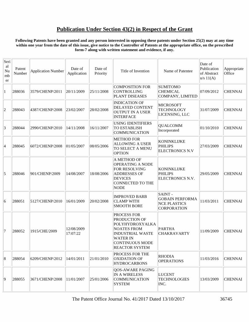
The Patent Office Journal No. 41/2017 Dated 13/10/2017 36745
Publication Under Section 43(2) in Respect of the Grant
Following Patents have been granted and any person interested in opposing these patents under Section 25(2) may at any time
within one year from the date of this issue, give notice to the Controller of Patents at the appropriate office, on the prescribed
form-7 along with written statement and evidence, if any.
Seri
al
Nu
mb
er
Patent
Number Application Number
Date of
Application
Date of
Priority Title of Invention Name of Patentee
Date of
Publication
of Abstract
u/s 11(A)
Appropriate
Office
1 288036 3579/CHENP/2011 20/11/2009 25/11/2008
COMPOSITION FOR
CONTROLLING
PLANT DISEASES
SUMITOMO
CHEMICAL
COMPANY, LIMITED
07/09/2012 CHENNAI
2 288043 4387/CHENP/2008 23/02/2007 28/02/2008
INDICATION OF
DELAYED CONTENT
OUTPUT IN A USER
INTERFACE
MICROSOFT
TECHNOLOGY
LICENSING, LLC
31/07/2009 CHENNAI
3 288044 2990/CHENP/2010 14/11/2008 16/11/2007
USING IDENTIFIERS
TO ESTABLISH
COMMUNICATION
QUALCOMM
Incorporated 01/10/2010 CHENNAI
4 288045 6072/CHENP/2008 01/05/2007 08/05/2006
METHOD FOR
ALLOWING A USER
TO SELECT A MENU
OPTION
KONINKLIJKE
PHILIPS
ELECTRONICS N.V
27/03/2009 CHENNAI
5 288046 901/CHENP/2009 14/08/2007 18/08/2006
A METHOD OF
OPERATING A NODE
FOR RESOLVING
ADDRESSES OF
DEVICES
CONNECTED TO THE
NODE
KONINKLIJKE
PHILIPS
ELECTRONICS N.V.
29/05/2009 CHENNAI
6 288051 5127/CHENP/2010 16/01/2009 20/02/2008
IMPROVED BARB
CLAMP WITH
SMOOTH BORE
SAINT -
GOBAIN PERFORMA
NCE PLASTICS
CORPORATION
11/03/2011 CHENNAI
7 288052 1915/CHE/2009 12/08/2009
17:07:22
PROCESS FOR
PRODUCTION OF
POLYHYDROXYALKA
NOATES FROM
INDUSTRIAL WASTE
WATER IN
CONTINUOUS MODE
REACTOR SYSTEM
PARTHA
CHAKRAVARTY 11/09/2009 CHENNAI
8 288054 6209/CHENP/2012 14/01/2011 21/01/2010
PROCESS FOR THE
OXIDATION OF
HYDROCARBONS
RHODIA
OPERATIONS 11/03/2016 CHENNAI
9 288055 3671/CHENP/2008 11/01/2007 25/01/2006
QOS-AWARE PAGING
IN A WIRELESS
COMMUNICATION
SYSTEM
LUCENT
TECHNOLOGIES
INC.
13/03/2009 CHENNAI
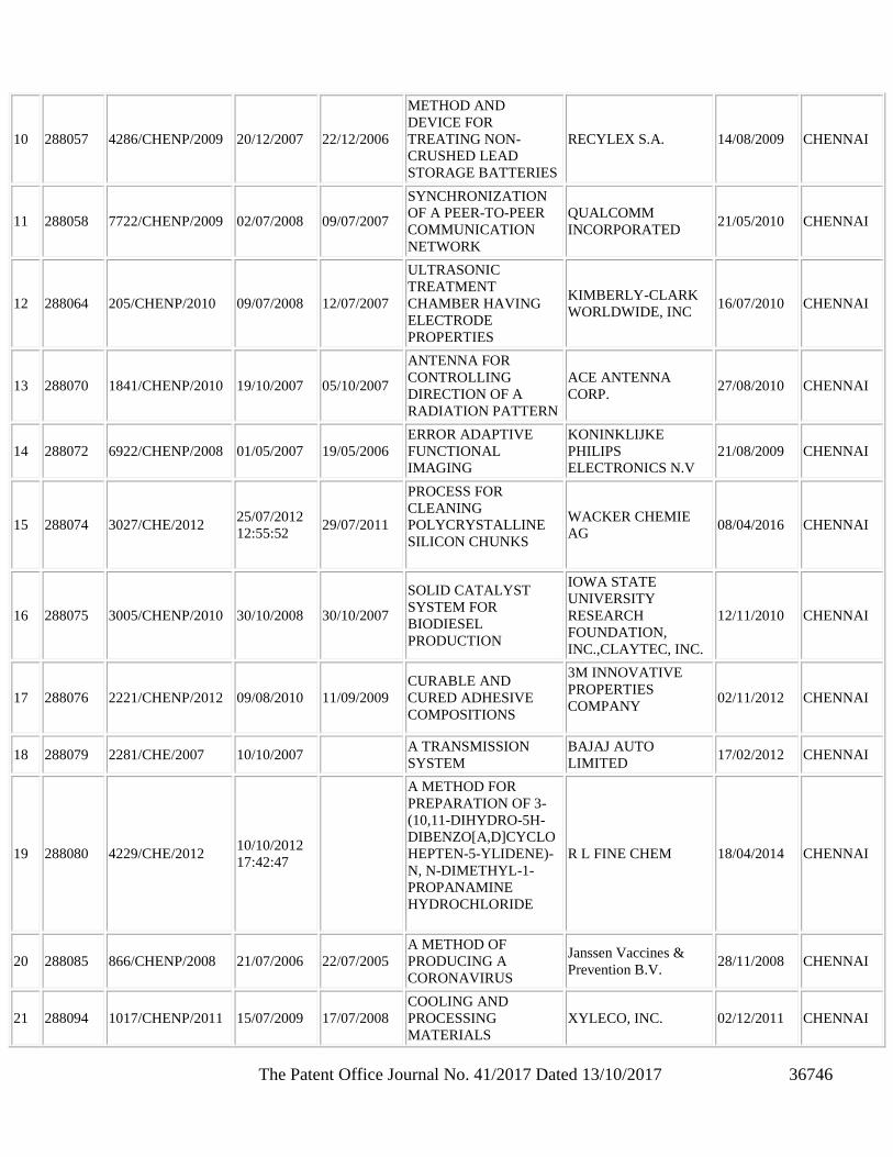
The Patent Office Journal No. 41/2017 Dated 13/10/2017 36746
10 288057 4286/CHENP/2009 20/12/2007 22/12/2006
METHOD AND
DEVICE FOR
TREATING NON-
CRUSHED LEAD
STORAGE BATTERIES
RECYLEX S.A. 14/08/2009 CHENNAI
11 288058 7722/CHENP/2009 02/07/2008 09/07/2007
SYNCHRONIZATION
OF A PEER-TO-PEER
COMMUNICATION
NETWORK
QUALCOMM
INCORPORATED 21/05/2010 CHENNAI
12 288064 205/CHENP/2010 09/07/2008 12/07/2007
ULTRASONIC
TREATMENT
CHAMBER HAVING
ELECTRODE
PROPERTIES
KIMBERLY-CLARK
WORLDWIDE, INC 16/07/2010 CHENNAI
13 288070 1841/CHENP/2010 19/10/2007 05/10/2007
ANTENNA FOR
CONTROLLING
DIRECTION OF A
RADIATION PATTERN
ACE ANTENNA
CORP. 27/08/2010 CHENNAI
14 288072 6922/CHENP/2008 01/05/2007 19/05/2006
ERROR ADAPTIVE
FUNCTIONAL
IMAGING
KONINKLIJKE
PHILIPS
ELECTRONICS N.V
21/08/2009 CHENNAI
15 288074 3027/CHE/2012 25/07/2012
12:55:52 29/07/2011
PROCESS FOR
CLEANING
POLYCRYSTALLINE
SILICON CHUNKS
WACKER CHEMIE
AG 08/04/2016 CHENNAI
16 288075 3005/CHENP/2010 30/10/2008 30/10/2007
SOLID CATALYST
SYSTEM FOR
BIODIESEL
PRODUCTION
IOWA STATE
UNIVERSITY
RESEARCH
FOUNDATION,
INC.,CLAYTEC, INC.
12/11/2010 CHENNAI
17 288076 2221/CHENP/2012 09/08/2010 11/09/2009
CURABLE AND
CURED ADHESIVE
COMPOSITIONS
3M INNOVATIVE
PROPERTIES
COMPANY
02/11/2012 CHENNAI
18 288079 2281/CHE/2007 10/10/2007 A TRANSMISSION
SYSTEM
BAJAJ AUTO
LIMITED 17/02/2012 CHENNAI
19 288080 4229/CHE/2012 10/10/2012
17:42:47
A METHOD FOR
PREPARATION OF 3-
(10,11-DIHYDRO-5H-
DIBENZO[A,D]CYCLO
HEPTEN-5-YLIDENE)-
N, N-DIMETHYL-1-
PROPANAMINE
HYDROCHLORIDE
R L FINE CHEM 18/04/2014 CHENNAI
20 288085 866/CHENP/2008 21/07/2006 22/07/2005
A METHOD OF
PRODUCING A
CORONAVIRUS
Janssen Vaccines &
Prevention B.V. 28/11/2008 CHENNAI
21 288094 1017/CHENP/2011 15/07/2009 17/07/2008
COOLING AND
PROCESSING
MATERIALS
XYLECO, INC. 02/12/2011 CHENNAI
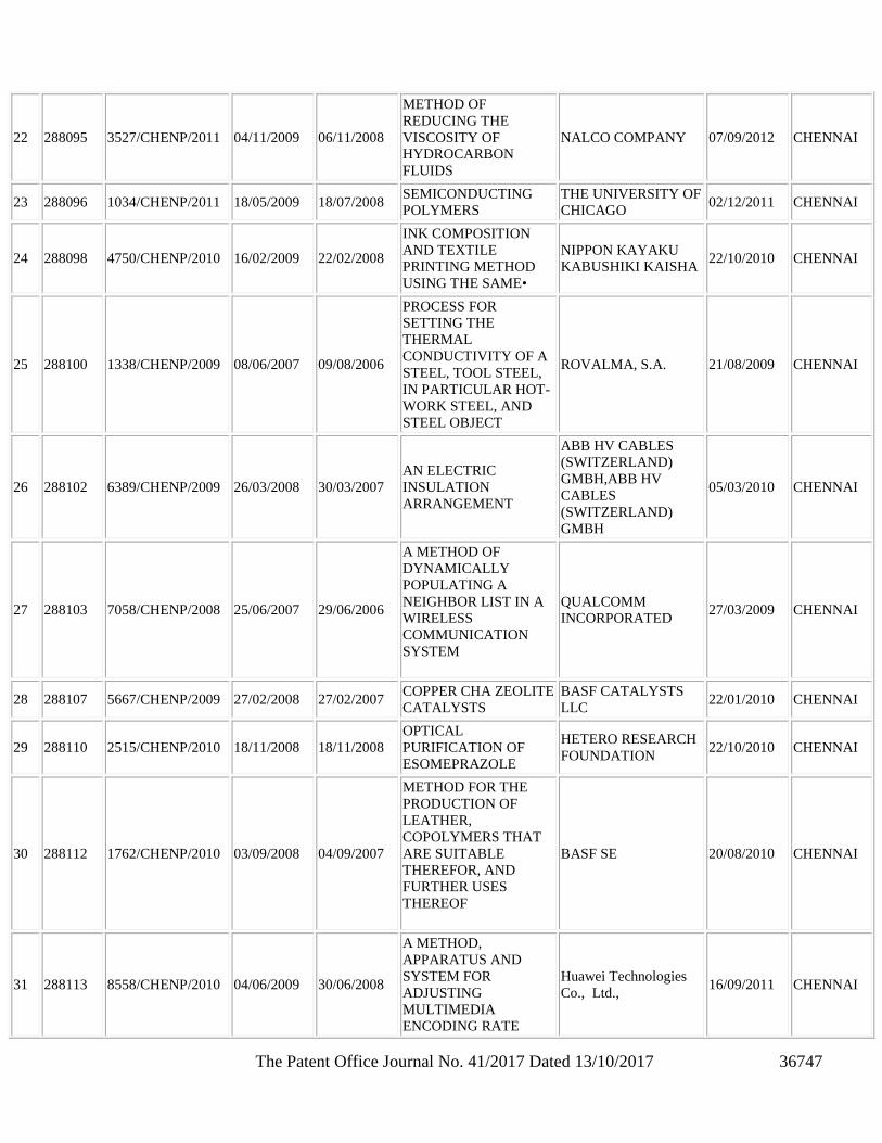
The Patent Office Journal No. 41/2017 Dated 13/10/2017 36747
22 288095 3527/CHENP/2011 04/11/2009 06/11/2008
METHOD OF
REDUCING THE
VISCOSITY OF
HYDROCARBON
FLUIDS
NALCO COMPANY 07/09/2012 CHENNAI
23 288096 1034/CHENP/2011 18/05/2009 18/07/2008 SEMICONDUCTING
POLYMERS
THE UNIVERSITY OF
CHICAGO 02/12/2011 CHENNAI
24 288098 4750/CHENP/2010 16/02/2009 22/02/2008
INK COMPOSITION
AND TEXTILE
PRINTING METHOD
USING THE SAME•
NIPPON KAYAKU
KABUSHIKI KAISHA 22/10/2010 CHENNAI
25 288100 1338/CHENP/2009 08/06/2007 09/08/2006
PROCESS FOR
SETTING THE
THERMAL
CONDUCTIVITY OF A
STEEL, TOOL STEEL,
IN PARTICULAR HOT-
WORK STEEL, AND
STEEL OBJECT
ROVALMA, S.A. 21/08/2009 CHENNAI
26 288102 6389/CHENP/2009 26/03/2008 30/03/2007
AN ELECTRIC
INSULATION
ARRANGEMENT
ABB HV CABLES
(SWITZERLAND)
GMBH,ABB HV
CABLES
(SWITZERLAND)
GMBH
05/03/2010 CHENNAI
27 288103 7058/CHENP/2008 25/06/2007 29/06/2006
A METHOD OF
DYNAMICALLY
POPULATING A
NEIGHBOR LIST IN A
WIRELESS
COMMUNICATION
SYSTEM
QUALCOMM
INCORPORATED 27/03/2009 CHENNAI
28 288107 5667/CHENP/2009 27/02/2008 27/02/2007 COPPER CHA ZEOLITE
CATALYSTS
BASF CATALYSTS
LLC 22/01/2010 CHENNAI
29 288110 2515/CHENP/2010 18/11/2008 18/11/2008
OPTICAL
PURIFICATION OF
ESOMEPRAZOLE
HETERO RESEARCH
FOUNDATION 22/10/2010 CHENNAI
30 288112 1762/CHENP/2010 03/09/2008 04/09/2007
METHOD FOR THE
PRODUCTION OF
LEATHER,
COPOLYMERS THAT
ARE SUITABLE
THEREFOR, AND
FURTHER USES
THEREOF
BASF SE 20/08/2010 CHENNAI
31 288113 8558/CHENP/2010 04/06/2009 30/06/2008
A METHOD,
APPARATUS AND
SYSTEM FOR
ADJUSTING
MULTIMEDIA
ENCODING RATE
Huawei Technologies
Co., Ltd., 16/09/2011 CHENNAI
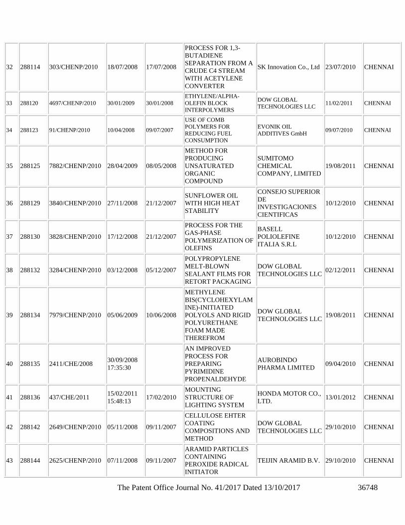
The Patent Office Journal No. 41/2017 Dated 13/10/2017 36748
32 288114 303/CHENP/2010 18/07/2008 17/07/2008
PROCESS FOR 1,3-
BUTADIENE
SEPARATION FROM A
CRUDE C4 STREAM
WITH ACETYLENE
CONVERTER
SK Innovation Co., Ltd 23/07/2010 CHENNAI
33 288120 4697/CHENP/2010 30/01/2009 30/01/2008
ETHYLENE/ALPHA-
OLEFIN BLOCK
INTERPOLYMERS
DOW GLOBAL
TECHNOLOGIES LLC 11/02/2011 CHENNAI
34 288123 91/CHENP/2010 10/04/2008 09/07/2007
USE OF COMB
POLYMERS FOR
REDUCING FUEL
CONSUMPTION
EVONIK OIL
ADDITIVES GmbH 09/07/2010 CHENNAI
35 288125 7882/CHENP/2010 28/04/2009 08/05/2008
METHOD FOR
PRODUCING
UNSATURATED
ORGANIC
COMPOUND
SUMITOMO
CHEMICAL
COMPANY, LIMITED
19/08/2011 CHENNAI
36 288129 3840/CHENP/2010 27/11/2008 21/12/2007
SUNFLOWER OIL
WITH HIGH HEAT
STABILITY
CONSEJO SUPERIOR
DE
INVESTIGACIONES
CIENTIFICAS
10/12/2010 CHENNAI
37 288130 3828/CHENP/2010 17/12/2008 21/12/2007
PROCESS FOR THE
GAS-PHASE
POLYMERIZATION OF
OLEFINS
BASELL
POLIOLEFINE
ITALIA S.R.L
10/12/2010 CHENNAI
38 288132 3284/CHENP/2010 03/12/2008 05/12/2007
POLYPROPYLENE
MELT-BLOWN
SEALANT FILMS FOR
RETORT PACKAGING
DOW GLOBAL
TECHNOLOGIES LLC 02/12/2011 CHENNAI
39 288134 7979/CHENP/2010 05/06/2009 10/06/2008
METHYLENE
BIS(CYCLOHEXYLAM
INE)-INITIATED
POLYOLS AND RIGID
POLYURETHANE
FOAM MADE
THEREFROM
DOW GLOBAL
TECHNOLOGIES LLC 19/08/2011 CHENNAI
40 288135 2411/CHE/2008 30/09/2008
17:35:30
AN IMPROVED
PROCESS FOR
PREPARING
PYRIMIDINE
PROPENALDEHYDE
AUROBINDO
PHARMA LIMITED 09/04/2010 CHENNAI
41 288136 437/CHE/2011 15/02/2011
15:48:13 17/02/2010
MOUNTING
STRUCTURE OF
LIGHTING SYSTEM
HONDA MOTOR CO.,
LTD. 13/01/2012 CHENNAI
42 288142 2649/CHENP/2010 05/11/2008 09/11/2007
CELLULOSE EHTER
COATING
COMPOSITIONS AND
METHOD
DOW GLOBAL
TECHNOLOGIES LLC 29/10/2010 CHENNAI
43 288144 2625/CHENP/2010 07/11/2008 09/11/2007
ARAMID PARTICLES
CONTAINING
PEROXIDE RADICAL
INITIATOR
TEIJIN ARAMID B.V. 29/10/2010 CHENNAI
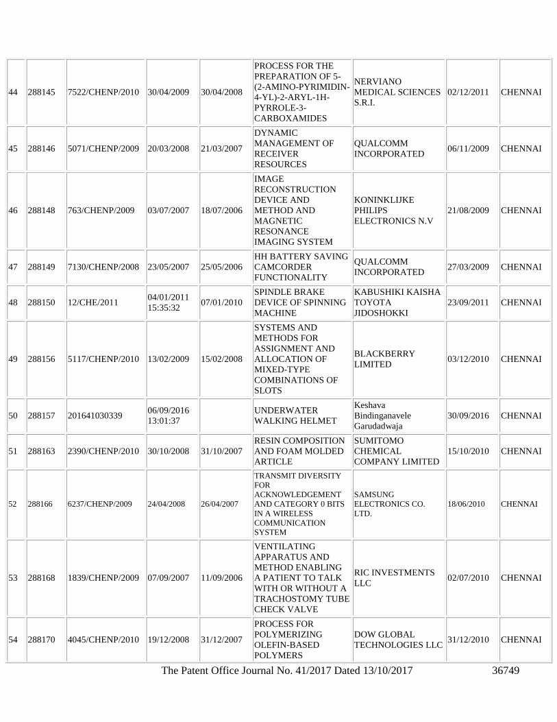
The Patent Office Journal No. 41/2017 Dated 13/10/2017 36749
44 288145 7522/CHENP/2010 30/04/2009 30/04/2008
PROCESS FOR THE
PREPARATION OF 5-
(2-AMINO-PYRIMIDIN-
4-YL)-2-ARYL-1H-
PYRROLE-3-
CARBOXAMIDES
NERVIANO
MEDICAL SCIENCES
S.R.I.
02/12/2011 CHENNAI
45 288146 5071/CHENP/2009 20/03/2008 21/03/2007
DYNAMIC
MANAGEMENT OF
RECEIVER
RESOURCES
QUALCOMM
INCORPORATED 06/11/2009 CHENNAI
46 288148 763/CHENP/2009 03/07/2007 18/07/2006
IMAGE
RECONSTRUCTION
DEVICE AND
METHOD AND
MAGNETIC
RESONANCE
IMAGING SYSTEM
KONINKLIJKE
PHILIPS
ELECTRONICS N.V
21/08/2009 CHENNAI
47 288149 7130/CHENP/2008 23/05/2007 25/05/2006
HH BATTERY SAVING
CAMCORDER
FUNCTIONALITY
QUALCOMM
INCORPORATED 27/03/2009 CHENNAI
48 288150 12/CHE/2011 04/01/2011
15:35:32 07/01/2010
SPINDLE BRAKE
DEVICE OF SPINNING
MACHINE
KABUSHIKI KAISHA
TOYOTA
JIDOSHOKKI
23/09/2011 CHENNAI
49 288156 5117/CHENP/2010 13/02/2009 15/02/2008
SYSTEMS AND
METHODS FOR
ASSIGNMENT AND
ALLOCATION OF
MIXED-TYPE
COMBINATIONS OF
SLOTS
BLACKBERRY
LIMITED 03/12/2010 CHENNAI
50 288157 201641030339 06/09/2016
13:01:37
UNDERWATER
WALKING HELMET
Keshava
Bindinganavele
Garudadwaja
30/09/2016 CHENNAI
51 288163 2390/CHENP/2010 30/10/2008 31/10/2007
RESIN COMPOSITION
AND FOAM MOLDED
ARTICLE
SUMITOMO
CHEMICAL
COMPANY LIMITED
15/10/2010 CHENNAI
52 288166 6237/CHENP/2009 24/04/2008 26/04/2007
TRANSMIT DIVERSITY
FOR
ACKNOWLEDGEMENT
AND CATEGORY 0 BITS
IN A WIRELESS
COMMUNICATION
SYSTEM
SAMSUNG
ELECTRONICS CO.
LTD.
18/06/2010 CHENNAI
53 288168 1839/CHENP/2009 07/09/2007 11/09/2006
VENTILATING
APPARATUS AND
METHOD ENABLING
A PATIENT TO TALK
WITH OR WITHOUT A
TRACHOSTOMY TUBE
CHECK VALVE
RIC INVESTMENTS
LLC 02/07/2010 CHENNAI
54 288170 4045/CHENP/2010 19/12/2008 31/12/2007
PROCESS FOR
POLYMERIZING
OLEFIN-BASED
POLYMERS
DOW GLOBAL
TECHNOLOGIES LLC 31/12/2010 CHENNAI
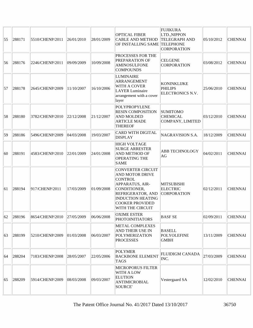
The Patent Office Journal No. 41/2017 Dated 13/10/2017 36750
55 288171 5510/CHENP/2011 26/01/2010 28/01/2009
OPTICAL FIBER
CABLE AND METHOD
OF INSTALLING SAME
FUJIKURA
LTD.,NIPPON
TELEGRAPH AND
TELEPHONE
CORPORATION
05/10/2012 CHENNAI
56 288176 2246/CHENP/2011 09/09/2009 10/09/2008
PROCESSES FOR THE
PREPARATION OF
AMINOSULFONE
COMPOUNDS
CELGENE
CORPORATION 03/08/2012 CHENNAI
57 288178 2645/CHENP/2009 11/10/2007 16/10/2006
LUMINAIRE
ARRANGEMENT
WITH A COVER
LAYER Luminaire
arrangement with a cover
layer
KONINKLIJKE
PHILIPS
ELECTRONICS N.V.
25/06/2010 CHENNAI
58 288180 3782/CHENP/2010 22/12/2008 21/12/2007
POLYPROPYLENE
RESIN COMPOSITION
AND MOLDED
ARTICLE MADE
THEREOF
SUMITOMO
CHEMICAL
COMPANY, LIMITED
03/12/2010 CHENNAI
59 288186 5496/CHENP/2009 04/03/2008 19/03/2007 CARD WITH DIGITAL
DISPLAY NAGRAVISION S.A. 18/12/2009 CHENNAI
60 288191 4583/CHENP/2010 22/01/2009 24/01/2008
HIGH VOLTAGE
SURGE ARRESTER
AND METHOD OF
OPERATING THE
SAME
ABB TECHNOLOGY
AG 04/02/2011 CHENNAI
61 288194 917/CHENP/2011 17/03/2009 01/09/2008
CONVERTER CIRCUIT
AND MOTOR DRIVE
CONTROL
APPARATUS, AIR-
CONDITIONER,
REFRIGERATOR, AND
INDUCTION HEATING
COOKER PROVIDED
WITH THE CIRCUIT
MITSUBISHI
ELECTRIC
CORPORATION
02/12/2011 CHENNAI
62 288196 8654/CHENP/2010 27/05/2009 06/06/2008 OXIME ESTER
PHOTOINITIATORS BASF SE 02/09/2011 CHENNAI
63 288199 5210/CHENP/2009 01/03/2008 06/03/2007
METAL COMPLEXES
AND THEIR USE IN
POLYMERIZATION
PROCESSES
BASELL
POLYOLEFINE
GMBH
13/11/2009 CHENNAI
64 288204 7183/CHENP/2008 28/05/2007 22/05/2006
POLYMER
BACKBONE ELEMENT
TAGS
FLUIDIGM CANADA
INC. 27/03/2009 CHENNAI
65 288209 5914/CHENP/2009 08/03/2008 09/03/2007
MICROPORUS FILTER
WITH A LOW
ELUTION
ANTIMICROBIAL
SOURCE'
Vestergaard SA 12/02/2010 CHENNAI
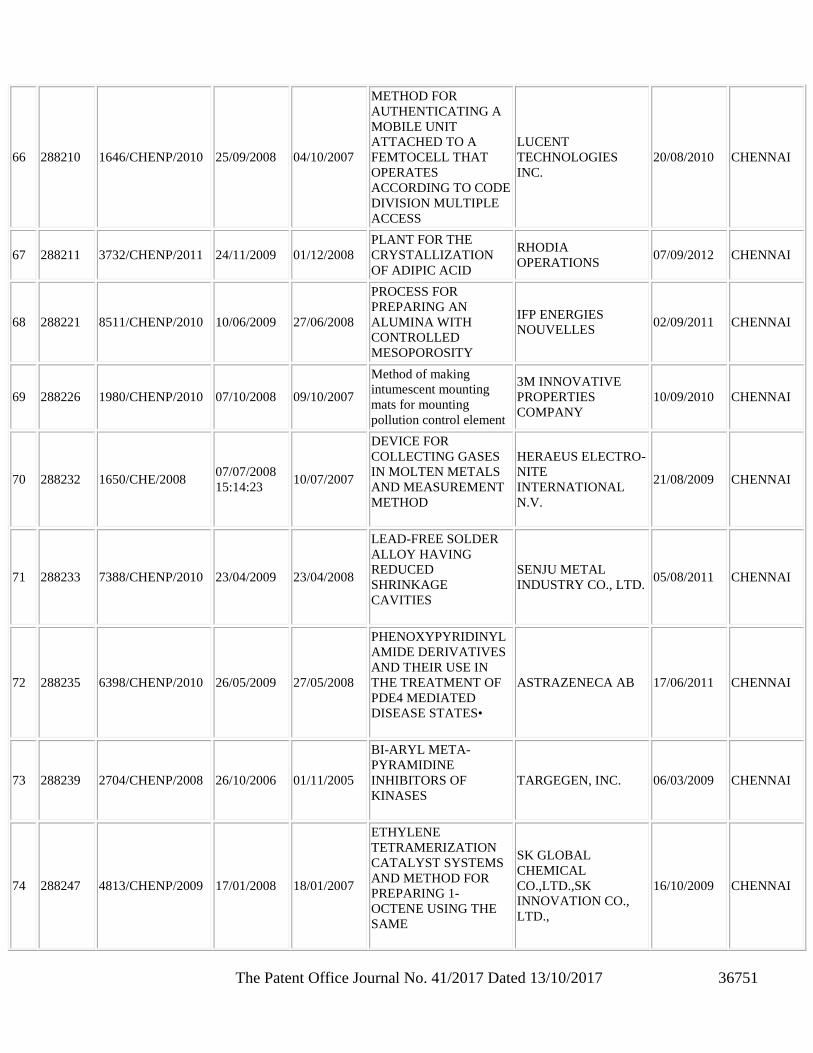
The Patent Office Journal No. 41/2017 Dated 13/10/2017 36751
66 288210 1646/CHENP/2010 25/09/2008 04/10/2007
METHOD FOR
AUTHENTICATING A
MOBILE UNIT
ATTACHED TO A
FEMTOCELL THAT
OPERATES
ACCORDING TO CODE
DIVISION MULTIPLE
ACCESS
LUCENT
TECHNOLOGIES
INC.
20/08/2010 CHENNAI
67 288211 3732/CHENP/2011 24/11/2009 01/12/2008
PLANT FOR THE
CRYSTALLIZATION
OF ADIPIC ACID
RHODIA
OPERATIONS 07/09/2012 CHENNAI
68 288221 8511/CHENP/2010 10/06/2009 27/06/2008
PROCESS FOR
PREPARING AN
ALUMINA WITH
CONTROLLED
MESOPOROSITY
IFP ENERGIES
NOUVELLES 02/09/2011 CHENNAI
69 288226 1980/CHENP/2010 07/10/2008 09/10/2007
Method of making
intumescent mounting
mats for mounting
pollution control element
3M INNOVATIVE
PROPERTIES
COMPANY
10/09/2010 CHENNAI
70 288232 1650/CHE/2008 07/07/2008
15:14:23 10/07/2007
DEVICE FOR
COLLECTING GASES
IN MOLTEN METALS
AND MEASUREMENT
METHOD
HERAEUS ELECTRO-
NITE
INTERNATIONAL
N.V.
21/08/2009 CHENNAI
71 288233 7388/CHENP/2010 23/04/2009 23/04/2008
LEAD-FREE SOLDER
ALLOY HAVING
REDUCED
SHRINKAGE
CAVITIES
SENJU METAL
INDUSTRY CO., LTD. 05/08/2011 CHENNAI
72 288235 6398/CHENP/2010 26/05/2009 27/05/2008
PHENOXYPYRIDINYL
AMIDE DERIVATIVES
AND THEIR USE IN
THE TREATMENT OF
PDE4 MEDIATED
DISEASE STATES•
ASTRAZENECA AB 17/06/2011 CHENNAI
73 288239 2704/CHENP/2008 26/10/2006 01/11/2005
BI-ARYL META-
PYRAMIDINE
INHIBITORS OF
KINASES
TARGEGEN, INC. 06/03/2009 CHENNAI
74 288247 4813/CHENP/2009 17/01/2008 18/01/2007
ETHYLENE
TETRAMERIZATION
CATALYST SYSTEMS
AND METHOD FOR
PREPARING 1-
OCTENE USING THE
SAME
SK GLOBAL
CHEMICAL
CO.,LTD.,SK
INNOVATION CO.,
LTD.,
16/10/2009 CHENNAI
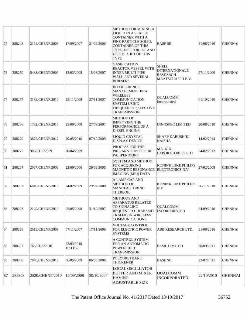
The Patent Office Journal No. 41/2017 Dated 13/10/2017 36752
75 288248 2164/CHENP/2009 17/09/2007 21/09/2006
METHOD FOR MIXING A
LIQUID IN A SEALED
CONTAINER WITH A
FINE-PARTICLE SOLID,
CONTAINER OF THIS
TYPE, EJECTOR JET AND
USE OF A JET OF THIS
TYPE
BASF SE 31/08/2016 CHENNAI
76 288250 5433/CHENP/2009 13/03/2008 15/03/2007
GASIFICATION
REACTOR VESSEL WITH
INNER MULTI-PIPE
WALL AND SEVERAL
BURNERS
SHELL
INTERNATIONALE
RESEARCH
MAATSCHAPPIJ B.V.
27/11/2009 CHENNAI
77 288257 3189/CHENP/2010 25/11/2008 27/11/2007
INTERFERENCE
MANAGEMENT IN A
WIRELESS
COMMUNICATION
SYSTEM USING
FREQUENCY SELECTIVE
TRANSMISSION
QUALCOMM
Incorporated 01/10/2010 CHENNAI
78 288266 1732/CHENP/2010 25/09/2008 27/09/2007
METHOD OF
IMPROVING THE
PERFORMANCE OF A
DIESEL ENGINE
INNOSPEC LIMITED 20/08/2010 CHENNAI
79 288270 3879/CHENP/2012 20/05/2010 07/10/2009 LIQUID CRYSTAL
DISPLAY DEVICE
SHARP KABUSHIKI
KAISHA 14/02/2014 CHENNAI
80 288277 903/CHE/2009 20/04/2009
PROCESS FOR THE
PREPARATION OF PURE
PALIPERIDONE
MATRIX
LABORATORIES LTD 24/02/2012 CHENNAI
81 288284 2037/CHENP/2008 22/09/2006 29/09/2005
SYSTEM AND METHOD
FOR ACQUIRING
MAGNETIC RESONANCE
IMAGING (MRI) DATA
KONINKLIJKE PHILIPS
ELECTRONICS N.V 27/02/2009 CHENNAI
82 288292 6049/CHENP/2010 24/02/2009 29/02/2008
A LAMP CAP AND
METHOD OF
MANUFACTURING
THEREOF.
KONINKLIJKE PHILIPS
N.V 26/11/2010 CHENNAI
83 288293 2129/CHENP/2010 05/05/2008 31/10/2007
METHODS AND
APPARATUS RELATED
TO SIGNALING
REQUEST TO TRANSMIT
TRAFFIC IN WIRELESS
COMMUNICATIONS
QUALCOMM
INCORPORATED 24/09/2010 CHENNAI
84 288296 2613/CHENP/2009 07/11/2007 17/11/2006
VOLTAGE CONTROL
FOR ELECTRIC POWER
SYSTEMS
ABB RESEARCH LTD; 31/08/2016 CHENNAI
85 288297 765/CHE/2010 22/03/2010
15:33:52
A CONTROL SYSTEM
FOR AN AUTOMATIC
POWERSHIFT
TRANSMISSION
BEML LIMITED 30/09/2011 CHENNAI
86 288306 7040/CHENP/2010 06/05/2009 06/05/2008 POLYURETHANE
THICKENER BASF SE 22/07/2011 CHENNAI
87 288308 2520/CHENP/2010 12/09/2008 30/10/2007
LOCAL OSCILLATOR
BUFFER AND MIXER
HAVING
ADJUSTABLE SIZE
QUALCOMM
INCORPORATED 22/10/2010 CHENNAI
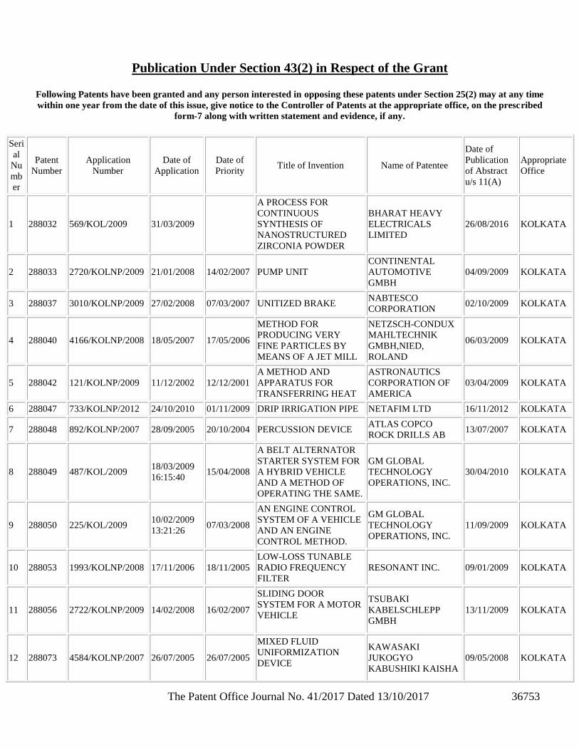
The Patent Office Journal No. 41/2017 Dated 13/10/2017 36753
Publication Under Section 43(2) in Respect of the Grant
Following Patents have been granted and any person interested in opposing these patents under Section 25(2) may at any time
within one year from the date of this issue, give notice to the Controller of Patents at the appropriate office, on the prescribed
form-7 along with written statement and evidence, if any.
Seri
al
Nu
mb
er
Patent
Number
Application
Number
Date of
Application
Date of
Priority Title of Invention Name of Patentee
Date of
Publication
of Abstract
u/s 11(A)
Appropriate
Office
1 288032 569/KOL/2009 31/03/2009
A PROCESS FOR
CONTINUOUS
SYNTHESIS OF
NANOSTRUCTURED
ZIRCONIA POWDER
BHARAT HEAVY
ELECTRICALS
LIMITED
26/08/2016 KOLKATA
2 288033 2720/KOLNP/2009 21/01/2008 14/02/2007 PUMP UNIT
CONTINENTAL
AUTOMOTIVE
GMBH
04/09/2009 KOLKATA
3 288037 3010/KOLNP/2009 27/02/2008 07/03/2007 UNITIZED BRAKE NABTESCO
CORPORATION 02/10/2009 KOLKATA
4 288040 4166/KOLNP/2008 18/05/2007 17/05/2006
METHOD FOR
PRODUCING VERY
FINE PARTICLES BY
MEANS OF A JET MILL
NETZSCH-CONDUX
MAHLTECHNIK
GMBH,NIED,
ROLAND
06/03/2009 KOLKATA
5 288042 121/KOLNP/2009 11/12/2002 12/12/2001
A METHOD AND
APPARATUS FOR
TRANSFERRING HEAT
ASTRONAUTICS
CORPORATION OF
AMERICA
03/04/2009 KOLKATA
6 288047 733/KOLNP/2012 24/10/2010 01/11/2009 DRIP IRRIGATION PIPE NETAFIM LTD 16/11/2012 KOLKATA
7 288048 892/KOLNP/2007 28/09/2005 20/10/2004 PERCUSSION DEVICE ATLAS COPCO
ROCK DRILLS AB 13/07/2007 KOLKATA
8 288049 487/KOL/2009 18/03/2009
16:15:40 15/04/2008
A BELT ALTERNATOR
STARTER SYSTEM FOR
A HYBRID VEHICLE
AND A METHOD OF
OPERATING THE SAME.
GM GLOBAL
TECHNOLOGY
OPERATIONS, INC.
30/04/2010 KOLKATA
9 288050 225/KOL/2009 10/02/2009
13:21:26 07/03/2008
AN ENGINE CONTROL
SYSTEM OF A VEHICLE
AND AN ENGINE
CONTROL METHOD.
GM GLOBAL
TECHNOLOGY
OPERATIONS, INC.
11/09/2009 KOLKATA
10 288053 1993/KOLNP/2008 17/11/2006 18/11/2005
LOW-LOSS TUNABLE
RADIO FREQUENCY
FILTER
RESONANT INC. 09/01/2009 KOLKATA
11 288056 2722/KOLNP/2009 14/02/2008 16/02/2007
SLIDING DOOR
SYSTEM FOR A MOTOR
VEHICLE
TSUBAKI
KABELSCHLEPP
GMBH
13/11/2009 KOLKATA
12 288073 4584/KOLNP/2007 26/07/2005 26/07/2005
MIXED FLUID
UNIFORMIZATION
DEVICE
KAWASAKI
JUKOGYO
KABUSHIKI KAISHA
09/05/2008 KOLKATA
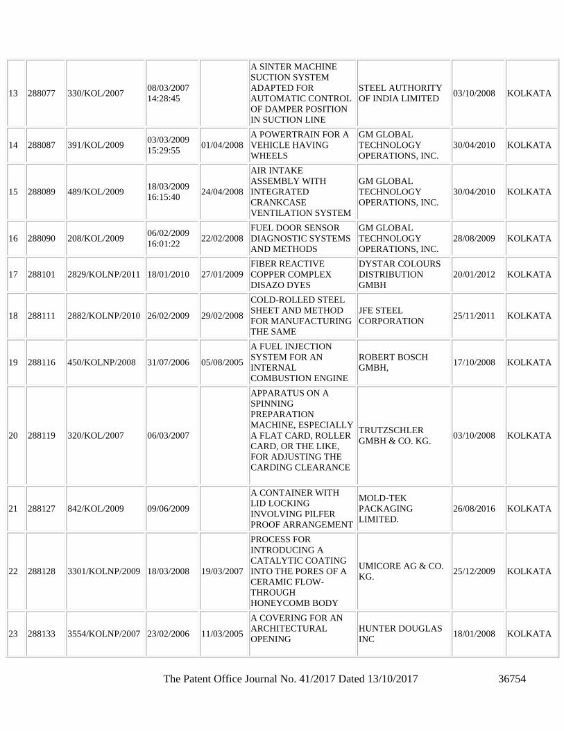
The Patent Office Journal No. 41/2017 Dated 13/10/2017 36754
13 288077 330/KOL/2007 08/03/2007
14:28:45
A SINTER MACHINE
SUCTION SYSTEM
ADAPTED FOR
AUTOMATIC CONTROL
OF DAMPER POSITION
IN SUCTION LINE
STEEL AUTHORITY
OF INDIA LIMITED 03/10/2008 KOLKATA
14 288087 391/KOL/2009 03/03/2009
15:29:55 01/04/2008
A POWERTRAIN FOR A
VEHICLE HAVING
WHEELS
GM GLOBAL
TECHNOLOGY
OPERATIONS, INC.
30/04/2010 KOLKATA
15 288089 489/KOL/2009 18/03/2009
16:15:40 24/04/2008
AIR INTAKE
ASSEMBLY WITH
INTEGRATED
CRANKCASE
VENTILATION SYSTEM
GM GLOBAL
TECHNOLOGY
OPERATIONS, INC.
30/04/2010 KOLKATA
16 288090 208/KOL/2009 06/02/2009
16:01:22 22/02/2008
FUEL DOOR SENSOR
DIAGNOSTIC SYSTEMS
AND METHODS
GM GLOBAL
TECHNOLOGY
OPERATIONS, INC.
28/08/2009 KOLKATA
17 288101 2829/KOLNP/2011 18/01/2010 27/01/2009
FIBER REACTIVE
COPPER COMPLEX
DISAZO DYES
DYSTAR COLOURS
DISTRIBUTION
GMBH
20/01/2012 KOLKATA
18 288111 2882/KOLNP/2010 26/02/2009 29/02/2008
COLD-ROLLED STEEL
SHEET AND METHOD
FOR MANUFACTURING
THE SAME
JFE STEEL
CORPORATION 25/11/2011 KOLKATA
19 288116 450/KOLNP/2008 31/07/2006 05/08/2005
A FUEL INJECTION
SYSTEM FOR AN
INTERNAL
COMBUSTION ENGINE
ROBERT BOSCH
GMBH, 17/10/2008 KOLKATA
20 288119 320/KOL/2007 06/03/2007
APPARATUS ON A
SPINNING
PREPARATION
MACHINE, ESPECIALLY
A FLAT CARD, ROLLER
CARD, OR THE LIKE,
FOR ADJUSTING THE
CARDING CLEARANCE
TRUTZSCHLER
GMBH & CO. KG. 03/10/2008 KOLKATA
21 288127 842/KOL/2009 09/06/2009
A CONTAINER WITH
LID LOCKING
INVOLVING PILFER
PROOF ARRANGEMENT
MOLD-TEK
PACKAGING
LIMITED.
26/08/2016 KOLKATA
22 288128 3301/KOLNP/2009 18/03/2008 19/03/2007
PROCESS FOR
INTRODUCING A
CATALYTIC COATING
INTO THE PORES OF A
CERAMIC FLOW-
THROUGH
HONEYCOMB BODY
UMICORE AG & CO.
KG. 25/12/2009 KOLKATA
23 288133 3554/KOLNP/2007 23/02/2006 11/03/2005
A COVERING FOR AN
ARCHITECTURAL
OPENING
HUNTER DOUGLAS
INC 18/01/2008 KOLKATA
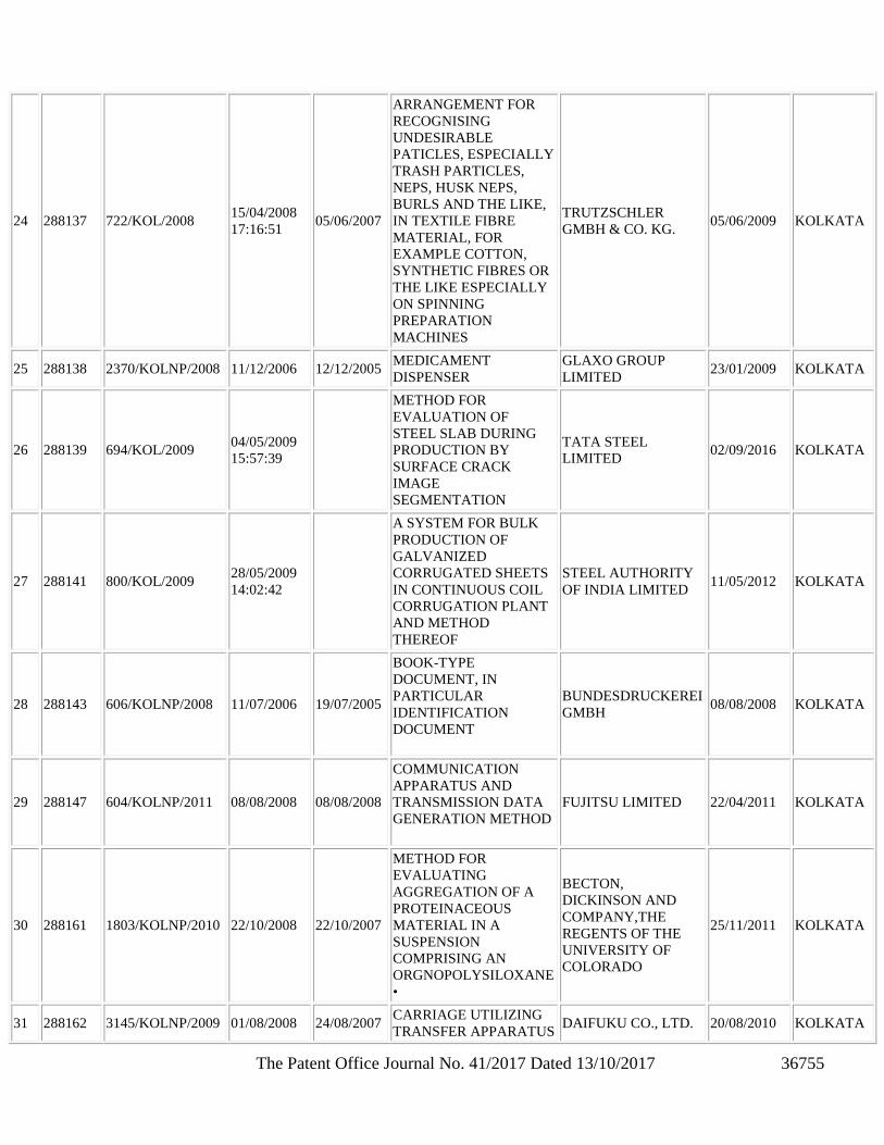
The Patent Office Journal No. 41/2017 Dated 13/10/2017 36755
24 288137 722/KOL/2008 15/04/2008
17:16:51 05/06/2007
ARRANGEMENT FOR
RECOGNISING
UNDESIRABLE
PATICLES, ESPECIALLY
TRASH PARTICLES,
NEPS, HUSK NEPS,
BURLS AND THE LIKE,
IN TEXTILE FIBRE
MATERIAL, FOR
EXAMPLE COTTON,
SYNTHETIC FIBRES OR
THE LIKE ESPECIALLY
ON SPINNING
PREPARATION
MACHINES
TRUTZSCHLER
GMBH & CO. KG. 05/06/2009 KOLKATA
25 288138 2370/KOLNP/2008 11/12/2006 12/12/2005 MEDICAMENT
DISPENSER
GLAXO GROUP
LIMITED 23/01/2009 KOLKATA
26 288139 694/KOL/2009 04/05/2009
15:57:39
METHOD FOR
EVALUATION OF
STEEL SLAB DURING
PRODUCTION BY
SURFACE CRACK
IMAGE
SEGMENTATION
TATA STEEL
LIMITED 02/09/2016 KOLKATA
27 288141 800/KOL/2009 28/05/2009
14:02:42
A SYSTEM FOR BULK
PRODUCTION OF
GALVANIZED
CORRUGATED SHEETS
IN CONTINUOUS COIL
CORRUGATION PLANT
AND METHOD
THEREOF
STEEL AUTHORITY
OF INDIA LIMITED 11/05/2012 KOLKATA
28 288143 606/KOLNP/2008 11/07/2006 19/07/2005
BOOK-TYPE
DOCUMENT, IN
PARTICULAR
IDENTIFICATION
DOCUMENT
BUNDESDRUCKEREI
GMBH 08/08/2008 KOLKATA
29 288147 604/KOLNP/2011 08/08/2008 08/08/2008
COMMUNICATION
APPARATUS AND
TRANSMISSION DATA
GENERATION METHOD
FUJITSU LIMITED 22/04/2011 KOLKATA
30 288161 1803/KOLNP/2010 22/10/2008 22/10/2007
METHOD FOR
EVALUATING
AGGREGATION OF A
PROTEINACEOUS
MATERIAL IN A
SUSPENSION
COMPRISING AN
ORGNOPOLYSILOXANE
•
BECTON,
DICKINSON AND
COMPANY,THE
REGENTS OF THE
UNIVERSITY OF
COLORADO
25/11/2011 KOLKATA
31 288162 3145/KOLNP/2009 01/08/2008 24/08/2007 CARRIAGE UTILIZING
TRANSFER APPARATUS DAIFUKU CO., LTD. 20/08/2010 KOLKATA
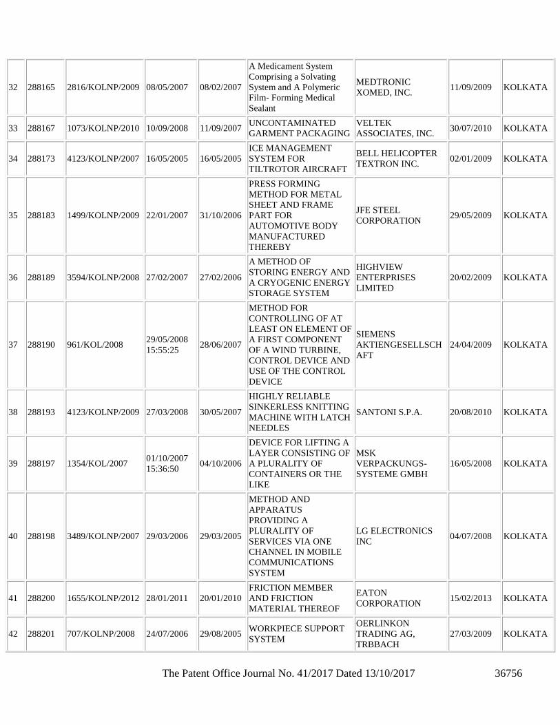
The Patent Office Journal No. 41/2017 Dated 13/10/2017 36756
32 288165 2816/KOLNP/2009 08/05/2007 08/02/2007
A Medicament System
Comprising a Solvating
System and A Polymeric
Film- Forming Medical
Sealant
MEDTRONIC
XOMED, INC. 11/09/2009 KOLKATA
33 288167 1073/KOLNP/2010 10/09/2008 11/09/2007 UNCONTAMINATED
GARMENT PACKAGING
VELTEK
ASSOCIATES, INC. 30/07/2010 KOLKATA
34 288173 4123/KOLNP/2007 16/05/2005 16/05/2005
ICE MANAGEMENT
SYSTEM FOR
TILTROTOR AIRCRAFT
BELL HELICOPTER
TEXTRON INC. 02/01/2009 KOLKATA
35 288183 1499/KOLNP/2009 22/01/2007 31/10/2006
PRESS FORMING
METHOD FOR METAL
SHEET AND FRAME
PART FOR
AUTOMOTIVE BODY
MANUFACTURED
THEREBY
JFE STEEL
CORPORATION 29/05/2009 KOLKATA
36 288189 3594/KOLNP/2008 27/02/2007 27/02/2006
A METHOD OF
STORING ENERGY AND
A CRYOGENIC ENERGY
STORAGE SYSTEM
HIGHVIEW
ENTERPRISES
LIMITED
20/02/2009 KOLKATA
37 288190 961/KOL/2008 29/05/2008
15:55:25 28/06/2007
METHOD FOR
CONTROLLING OF AT
LEAST ON ELEMENT OF
A FIRST COMPONENT
OF A WIND TURBINE,
CONTROL DEVICE AND
USE OF THE CONTROL
DEVICE
SIEMENS
AKTIENGESELLSCH
AFT
24/04/2009 KOLKATA
38 288193 4123/KOLNP/2009 27/03/2008 30/05/2007
HIGHLY RELIABLE
SINKERLESS KNITTING
MACHINE WITH LATCH
NEEDLES
SANTONI S.P.A. 20/08/2010 KOLKATA
39 288197 1354/KOL/2007 01/10/2007
15:36:50 04/10/2006
DEVICE FOR LIFTING A
LAYER CONSISTING OF
A PLURALITY OF
CONTAINERS OR THE
LIKE
MSK
VERPACKUNGS-
SYSTEME GMBH
16/05/2008 KOLKATA
40 288198 3489/KOLNP/2007 29/03/2006 29/03/2005
METHOD AND
APPARATUS
PROVIDING A
PLURALITY OF
SERVICES VIA ONE
CHANNEL IN MOBILE
COMMUNICATIONS
SYSTEM
LG ELECTRONICS
INC 04/07/2008 KOLKATA
41 288200 1655/KOLNP/2012 28/01/2011 20/01/2010
FRICTION MEMBER
AND FRICTION
MATERIAL THEREOF
EATON
CORPORATION 15/02/2013 KOLKATA
42 288201 707/KOLNP/2008 24/07/2006 29/08/2005 WORKPIECE SUPPORT
SYSTEM
OERLINKON
TRADING AG,
TRBBACH
27/03/2009 KOLKATA
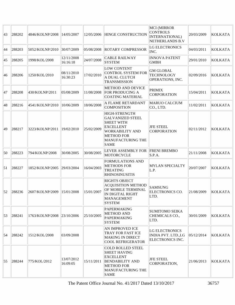
The Patent Office Journal No. 41/2017 Dated 13/10/2017 36757
43 288202 4846/KOLNP/2008 14/05/2007 12/05/2006 HINGE CONSTRUCTION
MCI (MIRROR
CONTROLS
INTERNATIONAL)
NETHERLANDS B.V
20/03/2009 KOLKATA
44 288203 5052/KOLNP/2010 30/07/2009 05/08/2008 ROTARY COMPRESSOR LG ELECTRONICS
INC. 04/03/2011 KOLKATA
45 288205 1998/KOL/2008 12/11/2008
16:16:18 24/07/2008
CABLE RAILWAY
SYSTEM
INNOVA PATENT
GMBH 29/01/2010 KOLKATA
46 288206 1250/KOL/2010 08/11/2010
16:30:23 17/02/2010
LOW CONTENT
CONTROL SYSTEM FOR
A DUAL CLUTCH
TRANSMISSION
GM GLOBAL
TECHNOLOGY
OPERATIONS, INC.
02/09/2016 KOLKATA
47 288208 430/KOLNP/2011 05/08/2009 11/08/2008
METHOD AND DEVICE
FOR PRODUCING A
COATING MATERIAL
PRIMIX
CORPORATION 15/04/2011 KOLKATA
48 288216 4541/KOLNP/2010 10/06/2009 18/06/2008 A FLAME RETARDANT
COMPOSITION
MARUO CALCIUM
CO., LTD. 11/02/2011 KOLKATA
49 288217 3223/KOLNP/2011 19/02/2010 25/02/2009
HIGH-STRENGTH
GALVANIZED STEEL
SHEET WITH
EXCELLENT
WORKABILITY AND
METHOD FOR
MANUFACTURING THE
SAME
JFE STEEL
CORPORATION 02/11/2012 KOLKATA
50 288223 794/KOLNP/2008 30/08/2005 30/08/2005 LEVER ASSEMBLY FOR
MOTORCYCLE
FRENI BREMBO
S.P.A. 21/11/2008 KOLKATA
51 288227 1852/KOLNP/2005 29/03/2004 16/04/2003
FORMULATIONS AND
METHODS FOR
TREATING
RHINOSINUSITIS
MYLAN SPECIALTY
L.P. 20/07/2007 KOLKATA
52 288236 2607/KOLNP/2009 15/01/2008 15/01/2007
RIGHTS OBJECT
ACQUISITION METHOD
OF MOBILE TERMINAL
IN DIGITAL RIGHT
MANAGEMENT
SYSTEM
SAMSUNG
ELECTRONICS CO.
LTD.
21/08/2009 KOLKATA
53 288241 1763/KOLNP/2008 23/10/2006 25/10/2005
PAPERMAKING
METHOD AND
PAPERMAKING
SYSTEM
SUMITOMO SEIKA
CHEMICALS CO.,
LTD.
30/01/2009 KOLKATA
54 288242 1512/KOL/2008 03/09/2008
AN IMPROVED ICE
TRAY FOR FAST ICE
MAKING IN DIRECT
COOL REFRIGERATOR
LG ELECTRONICS
INDIA PVT. LTD.,LG
ELECTRONICS INC.
05/12/2014 KOLKATA
55 288244 775/KOL/2012 13/07/2012
16:09:05 15/11/2011
COLD ROLLED STEEL
SHEET HAVING
EXCELLENT
BENDABILITY AND
METHOD FOR
MANUFACTURING THE
SAME
JFE STEEL
CORPORATION, 21/06/2013 KOLKATA
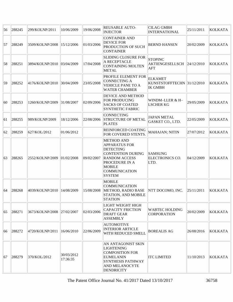
The Patent Office Journal No. 41/2017 Dated 13/10/2017 36758
56 288245 299/KOLNP/2011 10/06/2009 19/06/2008 REUSABLE AUTO-
INJECTOR
CILAG GMBH
INTERNATIONAL 25/11/2011 KOLKATA
57 288249 3509/KOLNP/2008 15/12/2006 01/03/2006
CONTAINER AND
DEVICE FOR
PRODUCTION OF SUCH
CONTAINER
BERND HANSEN 20/02/2009 KOLKATA
58 288251 3894/KOLNP/2010 03/04/2009 17/04/2008
SLIDING CLOSURE FOR
A RECEPTACLE
CONTAINING MOLTEN
METAL
STOPINC
AKTIENGESELLSCH
AFT
24/12/2010 KOLKATA
59 288252 4176/KOLNP/2010 30/04/2009 23/05/2008
PROFILE ELEMENT FOR
CONNECTING A
VEHICLE PANE TO A
WATER CHAMBER
ELKAMET
KUNSTSTOFFTECHN
IK GMBH
31/12/2010 KOLKATA
60 288253 1260/KOLNP/2009 31/08/2007 02/09/2006
DEVICE AND METHOD
FOR PRODUCING
SACKS OF COATED
SYNTHETIC FABRIC
WINDM–LLER & H–
LSCHER KG 29/05/2009 KOLKATA
61 288255 989/KOLNP/2009 18/12/2006 22/08/2006
CONNECTING
STRUCTURE OF METAL
PLATES
JAPAN METAL
GASKET CO., LTD. 22/05/2009 KOLKATA
62 288259 627/KOL/2012 01/06/2012 REINFORCED COATING
FOR COVERED STENTS. MAHAJAN; NITIN 27/07/2012 KOLKATA
63 288265 2552/KOLNP/2009 01/02/2008 09/02/2007
METHOD AND
APPARATUS FOR
DETECTING
CONTENTION DURING
RANDOM ACCESS
PROCEDURE IN A
MOBILE
COMMUNICATION
SYSTEM
SAMSUNG
ELECTRONICS CO.
LTD.
04/12/2009 KOLKATA
64 288268 4039/KOLNP/2010 14/08/2009 15/08/2008
MOBILE
COMMUNICATION
METHOD, RADIO BASE
STATION, AND MOBILE
STATION
NTT DOCOMO, INC. 25/11/2011 KOLKATA
65 288271 3673/KOLNP/2008 27/02/2007 02/03/2006
LIGHT WEIGHT HIGH
CAPACITY FRICTION
DRAFT GEAR
ASSEMBLY
WABTEC HOLDING
CORPORATION 20/02/2009 KOLKATA
66 288272 4720/KOLNP/2011 16/06/2010 22/06/2009
AUTOMOTIVE
INTERIOR ARTICLE
WITH REDUCED SMELL
BOREALIS AG 26/08/2016 KOLKATA
67 288279 370/KOL/2012 30/03/2012
17:36:35
AN ANTAGONIST SKIN
LIGHTENING
COMPOSITION FOR
EUMELANIN
SYNTHESIS PATHWAY
AND MELANOCYTE
DENDRICITY
ITC LIMITED 11/10/2013 KOLKATA
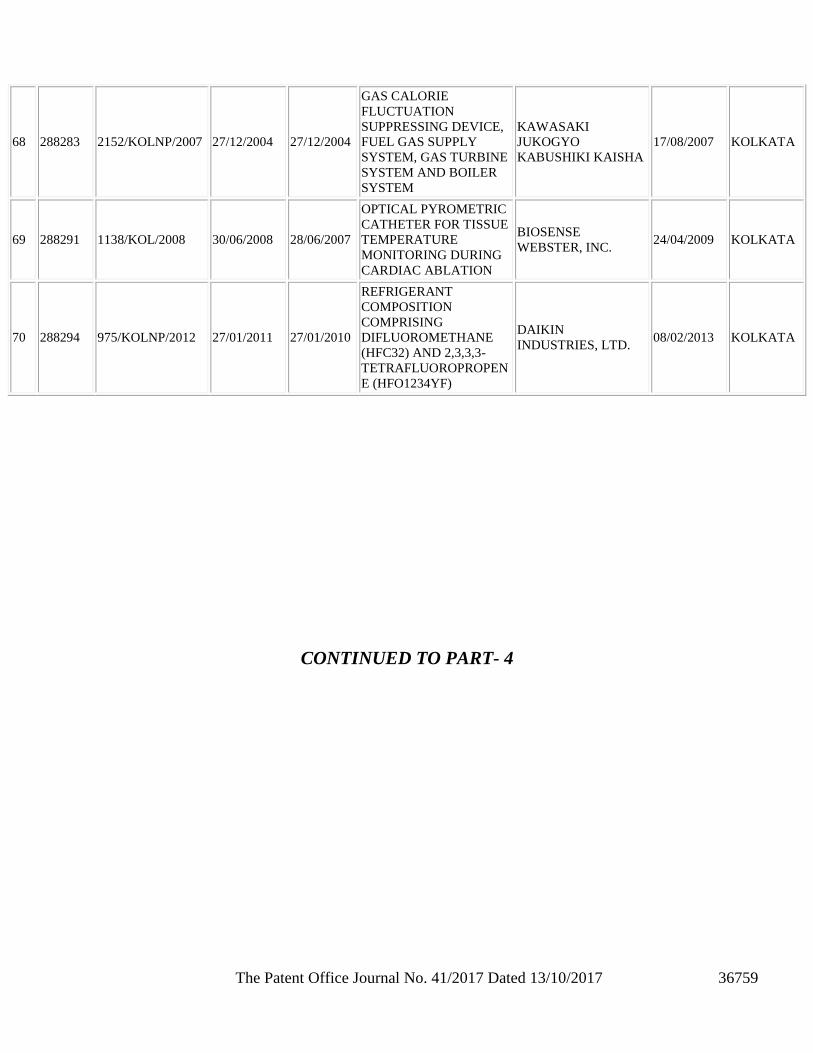
The Patent Office Journal No. 41/2017 Dated 13/10/2017 36759
68 288283 2152/KOLNP/2007 27/12/2004 27/12/2004
GAS CALORIE
FLUCTUATION
SUPPRESSING DEVICE,
FUEL GAS SUPPLY
SYSTEM, GAS TURBINE
SYSTEM AND BOILER
SYSTEM
KAWASAKI
JUKOGYO
KABUSHIKI KAISHA
17/08/2007 KOLKATA
69 288291 1138/KOL/2008 30/06/2008 28/06/2007
OPTICAL PYROMETRIC
CATHETER FOR TISSUE
TEMPERATURE
MONITORING DURING
CARDIAC ABLATION
BIOSENSE
WEBSTER, INC. 24/04/2009 KOLKATA
70 288294 975/KOLNP/2012 27/01/2011 27/01/2010
REFRIGERANT
COMPOSITION
COMPRISING
DIFLUOROMETHANE
(HFC32) AND 2,3,3,3-
TETRAFLUOROPROPEN
E (HFO1234YF)
DAIKIN
INDUSTRIES, LTD. 08/02/2013 KOLKATA
CONTINUED TO PART- 4
Related Documents