Title Reference Design Report for 1.6 W, Linear Replacement Adapter with 10 kV surge withstand Specification 85–265 VAC Input, 7.7 V, 210 mA Output Application Cordless Phone Adapter Author Power Integrations Applications Department Document Number RDR-83 Date Sept 29, 2006 Revision 1.0 Summary and Features • Highly efficient, low cost switching solution • Replacement for existing AC line transformer based design • Designed to withstand 10 kV common-mode surges • Ideal for applications connected to telephone network • EcoSmart ® – meets all existing and proposed harmonized energy efficiency standards including: CECP (China), CEC, EPA, AGO, European Commission • No-load power consumption <220 mW at 265 VAC • 61.3% active-mode efficiency (exceeds requirement of 53.2%) • Integrated LinkSwitch safety/reliability features: • Accurate (± 5%), auto-recovering, hysteretic thermal shutdown function maintains safe PCB temperatures under all conditions • Auto-restart protects against output short circuits and open feedback loops • Meets EN55022 and CISPR-22 Class B conducted EMI with >15 dBμV margin • Meets IEC61000-4-5 Class 4 AC line surge The products and applications illustrated herein (including circuits external to the products and transformer construction) may be covered by one or more U.S. and foreign patents or potentially by pending U.S. and foreign patent applications assigned to Power Integrations. A complete list of Power Integrations’ patents may be found at www.powerint.com.

Welcome message from author
This document is posted to help you gain knowledge. Please leave a comment to let me know what you think about it! Share it to your friends and learn new things together.
Transcript
Title Reference Design Report for 1.6 W, Linear Replacement Adapter with 10 kV surge withstand
Specification 85–265 VAC Input, 7.7 V, 210 mA Output
Application Cordless Phone Adapter
Author Power Integrations Applications Department
Document Number RDR-83
Date Sept 29, 2006
Revision 1.0
Summary and Features • Highly efficient, low cost switching solution
• Replacement for existing AC line transformer based design • Designed to withstand 10 kV common-mode surges
• Ideal for applications connected to telephone network • EcoSmart® – meets all existing and proposed harmonized energy efficiency
standards including: CECP (China), CEC, EPA, AGO, European Commission • No-load power consumption <220 mW at 265 VAC • 61.3% active-mode efficiency (exceeds requirement of 53.2%)
• Integrated LinkSwitch safety/reliability features: • Accurate (± 5%), auto-recovering, hysteretic thermal shutdown function
maintains safe PCB temperatures under all conditions • Auto-restart protects against output short circuits and open feedback loops
• Meets EN55022 and CISPR-22 Class B conducted EMI with >15 dBµV margin • Meets IEC61000-4-5 Class 4 AC line surge
The products and applications illustrated herein (including circuits external to the products and transformer construction) may be covered by one or more U.S. and foreign patents or potentially by pending U.S. and foreign patent applications assigned to Power Integrations. A complete list of Power Integrations’ patents may be found at www.powerint.com.

RDR-83 7.7 V, 210 mA Adapter with 10 kV surge withstand 29-Sept-06
Page 2 of 36
Power Integrations Tel: +1 408 414 9200 Fax: +1 408 414 9201www.powerint.com
Table Of Contents 1 Introduction.................................................................................................................3 2 Power Supply Specification ........................................................................................4
2.1 Typical Output Characteristic and limits ..............................................................5 3 Schematic...................................................................................................................6 4 Circuit Description ......................................................................................................7
4.1 Input Stage ..........................................................................................................7 4.2 LinkSwitch-LP......................................................................................................7 4.3 Feedback.............................................................................................................8 4.4 Output Rectification .............................................................................................9
5 PCB Layout ..............................................................................................................10 6 Bill Of Materials ........................................................................................................11 7 Transformer Specification.........................................................................................12
7.1 Electrical Diagram .............................................................................................12 7.2 Electrical Specifications.....................................................................................12 7.3 Materials............................................................................................................12 7.4 Transformer Build Diagram ...............................................................................13 7.5 Transformer Construction..................................................................................13
8 Design Spreadsheets ...............................................................................................14 9 Performance Data ....................................................................................................19
9.1 Efficiency ...........................................................................................................19 9.1.1 Active Mode ENERGY STAR / CEC Efficiency Measurement Data...........20
9.2 No-load Input Power..........................................................................................21 9.3 Available Standby Output Power.......................................................................21 9.4 Regulation .........................................................................................................22
9.4.1 VI Curve vs. Input Voltage..........................................................................22 10 Thermal Performance ...........................................................................................23
10.1 LNK562 Temperature Rise................................................................................23 10.2 Thermal Image ..................................................................................................23
11 Waveforms............................................................................................................24 11.1 Drain Voltage and Current, Normal Operation...................................................24 11.2 Output Voltage Start-up Profile..........................................................................24 11.3 Drain Voltage and Current Start-up Profile ........................................................25 11.4 Load Transient Response (50% to 100% Load Step) .......................................26 11.5 Output Ripple Measurements............................................................................27
11.5.1 Ripple Measurement Technique ................................................................27 11.5.2 Measurement Results ................................................................................28
12 Line Surge.............................................................................................................29 13 Conducted EMI .....................................................................................................30 14 Revision History ....................................................................................................32 Important Note: Although this board is designed to satisfy safety isolation requirements, the engineering prototype has not been agency approved. Therefore, all testing should be performed using an isolation transformer to provide the AC input to the prototype board.

29-Sept-06 RDR-83 7.7 V, 210 mA Adapter with 10 kV surge withstand
Page 3 of 36
Power IntegrationsTel: +1 408 414 9200 Fax: +1 408 414 9201
www.powerint.com
1 Introduction This reference design report describes a switched-mode power supply that was designed to replace line frequency transformer based solutions. The supply uses a member of the LinkSwitch-LP family of devices, and is capable of withstanding common-mode line surges of up to 10 kV. That is often a requirement for applications that connect to a telephone line, such as modems, cordless phones and answering machines. The report includes the power supply specification, a circuit diagram, a bill of materials, transformer documentation, a printed circuit layout board, and performance data.
Figure 1 – Populated Circuit Board Photograph.

RDR-83 7.7 V, 210 mA Adapter with 10 kV surge withstand 29-Sept-06
Page 4 of 36
Power Integrations Tel: +1 408 414 9200 Fax: +1 408 414 9201www.powerint.com
2 Power Supply Specification
Description Symbol Min Typ Max Units Comment Input Voltage VIN 85 265 VAC 2 Wire – no P.E. Frequency fLINE 47 50/60 64 Hz No-load Input Power (230 VAC) 0.3 W
Output Output Voltage 1 VOUT1 6.7 7.7 8.7 V Output Ripple Voltage 1 VRIPPLE1 400 mV 20 MHz bandwidth Output Current 1 IOUT1 0.21 0.21 A
Total Output Power
Continuous Output Power POUT 1.4 1.6 W No Load Output Voltage 11 V
Efficiency Full Load η 60 % Measured at POUT 25 oC
Required average efficiency at 25, 50, 75 and 100 % of POUT ηCEC 53 % Per ENERGY STAR / CEC
requirements
Environmental
Conducted EMI Meets CISPR22B / EN55022B
Safety Designed to meet IEC950, UL1950 Class II
Surge Differential Mode Common Mode
2 6
10
kV kV
1.2/50 µs surge, IEC 1000-4-5, Series Impedance:
Differential Mode: 2 Ω Common Mode: 12 Ω
Surge 2 KV 100 kHz ring wave, 500 A short circuit current, differential
Ambient Temperature TAMB 0 50 oC Free convection, sea level

29-Sept-06 RDR-83 7.7 V, 210 mA Adapter with 10 kV surge withstand
Page 5 of 36
Power IntegrationsTel: +1 408 414 9200 Fax: +1 408 414 9201
www.powerint.com
2.1 Typical Output Characteristic and Limits The following diagram shows the output characteristic of the LinkSwitch-LP solution and that of the linear transformer solution it was designed to replace. As can be seen, the LinkSwitch-LP solution provides a more controlled output characteristic.
Figure 2 – Output Characteristic Comparison and Limits.
0
2
4
6
8
10
12
14
16
18
0 0.1 0.2 0.3 0.4 0.5 0.6 0.7 0.8
Amps
Volts
UPPER LIMITLOWER LIMITLinear AdapterRD-83 115 VAC
115 VAC
RDR-83 7.7 V, 210 mA Adapter with 10 kV surge withstand 29-Sept-06
Page 6 of 36
Power Integrations Tel: +1 408 414 9200 Fax: +1 408 414 9201www.powerint.com
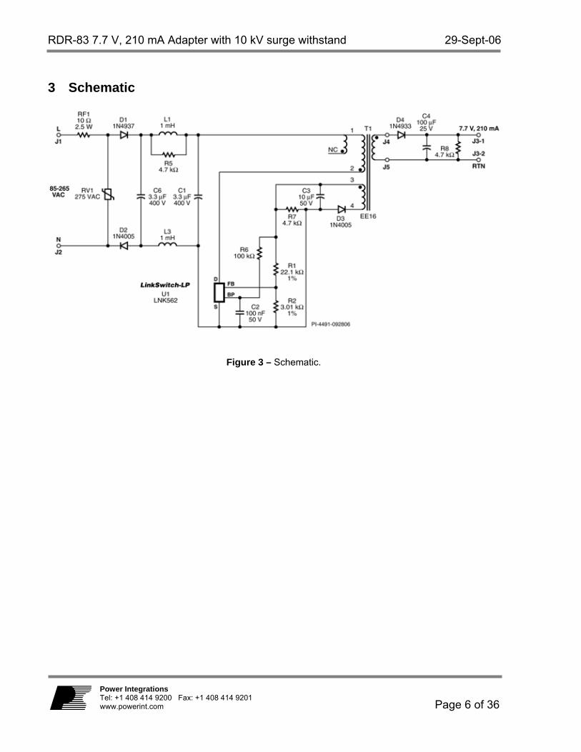
3 Schematic
Figure 3 – Schematic.

29-Sept-06 RDR-83 7.7 V, 210 mA Adapter with 10 kV surge withstand
Page 7 of 36
Power IntegrationsTel: +1 408 414 9200 Fax: +1 408 414 9201
www.powerint.com
4 Circuit Description
4.1 Input Stage Components C1, C6, L1 and L3 comprise a balanced π filter. Resistor R5 dampens low frequency conducted EMI. The supply needs no Y1-type capacitor (that normally bridges the primary to secondary isolation barrier) due to U1’s frequency jitter function and the E-Shield™ techniques used in the design of transformer T1. This minimizes audible noise in applications connected to a phone line, by eliminating a path for line frequency leakage currents to pass onto the output of the supply. The supply easily meets EN55022B conducted EMI limits, with more than 15 dBµV of margin. A metal oxide varistor (RV1) and a wire wound resistor (RF1) attenuate differential line surges. The varistor is required to meet the 2 kV differential surge requirement. In applications where only 1 kV of surge immunity is required, RV1 can be eliminated. The wire wound resistor (RF1) must be able to withstand high transient dissipation from initial inrush current (when AC power is applied) and during line surges.
4.2 LinkSwitch-LP The LinkSwitch-LP family of ICs were designed to replace linear transformer solutions in low-power charger and adapter applications. Feedback to the LNK562P IC (U1) is derived from a resistor divider (R1 and R2) across the bias supply (D3 and C3), which lowers cost by eliminating the need for an optocoupler. Linear transformers typically use thermal fuses (over temperature cut-outs) for overload protection. However, once a thermal fuse trips, the entire charger or adapter must be thrown away, since thermal fuses cannot be reset or repaired. Latching thermal shutdown functions are typically used in ringing choke converter (RCC) based supplies. However, AC input power must be removed and reapplied to reset most thermal latches. Since customers typically don’t know this, they often return good units they thought were defective, simply because the thermal latch tripped and shut the unit off. The LinkSwitch-LP family’s hysteretic thermal shutdown function has a very tight tolerance (142 °C, ±5%), and automatically restarts the power supply once the IC temperature drops below the lower temperature threshold. This maintains the average PCB temperature at a safe level under all conditions, and reduces the return rate of good units from the field. The auto-recovery feature also eliminates the noise sensitivity and component aging problems associated with discrete latching circuits. Pin 6 is eliminated from the IC package to extend the creepage distance between the DRAIN pin and all other low voltage pins; both at the package and on the PCB. This reduces the likelihood that tracking or arcing will occur due to moisture or board surface contamination (from dust and dirt), which improves reliability in high humidity and high pollution environments. During an output short circuit or an open loop condition, the LinkSwitch-LP’s auto-restart function limits output power to about 12% of the maximum. This protects both the load and the supply during prolonged overload conditions.
RDR-83 7.7 V, 210 mA Adapter with 10 kV surge withstand 29-Sept-06
Page 8 of 36
Power Integrations Tel: +1 408 414 9200 Fax: +1 408 414 9201www.powerint.com
The LinkSwitch-LP family of ICs are self-biased, via a high-voltage current source that is internally connected to the DRAIN pin of the package. A capacitor (C2) connected to the BYPASS (BP) pin of the IC provides energy storage and local decoupling of the internal chip power. To further reduce no-load power consumption, a resistor can be used to provide operating current to the IC from the bias winding (once the power supply is operating). In this design, the bias winding voltage is about 14 V and the BP pin voltage is 5.8 V. Therefore, R6 (100 kΩ) provides about 80 µA of current to the BP pin. If the value of R6 were reduced, it could provide the entire 220 µA of IC supply current, which would further reduce the no-load power consumption of the supply. The worst-case, no-load power consumption of this supply is approximately 200 mW at an input voltage of 265 VAC, which is well below the maximum limit of most energy efficiency standards. Heat generation is also kept to a minimum in this design, given the high operating efficiency at all line and load conditions.
4.3 Feedback The output voltage of the supply is regulated based on feedback from the primary-side bias supply. The bias winding voltage is rectified and filtered by D3 and C3. The leakage inductance between the output winding and the bias winding induces error in the bias winding voltage. Using a standard rectifier diode for D3 makes the bias winding voltage more accurately track the output voltage. Resistor R7 preloads (3 mA) the output of the bias supply, which further reduces the error and also limits the no-load output voltage. A resistor divider (R1 and R2) provides the feedback voltage to the FB pin of U1. The values of R1 and R2 are selected so that when the output voltage is at the desired nominal value, the voltage on the FB pin is 1.69 V, and about 70 µA flows into the FB pin. The LinkSwitch-LP family of devices use ON/OFF control to regulate the output of the supply. During constant voltage (CV) operation, switching cycles are skipped when the current into the FB pin exceeds 70 µA. As the load on the output of the supply reduces, more switching cycles are skipped. As the load increases, fewer cycles are skipped. The result is that the average or effective switching frequency varies with the load. This makes the efficiency fairly consistent over the entire load range, since the switching losses scale with the load on the output of the supply. When the load on the output of the supply reaches its maximum power capability, no switching cycles are skipped. If the load is increased beyond that point, the output voltage of the supply will start to drop. As the output voltage drops, the voltage on the FB pin also drops, and the IC linearly reduces its switching frequency. This keeps the output current from increasing significantly. Once the FB pin voltage falls below 0.8 V for more than 100 ms, all LinkSwitch-LP devices enter an auto-restart mode. While in auto-restart, the controller enables MOSFET switching for 100 ms. If the FB pin voltage does not exceed 0.8 V during the 100 ms, the controller disables MOSFET switching. MOSFET switching is alternately enabled and disables at a duty cycle of about 12% until the fault condition clears. This protects both the supply and the load.

29-Sept-06 RDR-83 7.7 V, 210 mA Adapter with 10 kV surge withstand
Page 9 of 36
Power IntegrationsTel: +1 408 414 9200 Fax: +1 408 414 9201
www.powerint.com
4.4 Output Rectification The transformer secondary winding is rectified by D4 and filtered by C4. A small preload resistor (R8) limits the no-load output voltage. Decreasing the value of the preload resistor will further reduce the no-load output voltage, at the expense of increasing the no-load input power consumption. In this design, a fast diode (rather than an ultra-fast) was used for D4 to lower cost and EMI emissions.
RDR-83 7.7 V, 210 mA Adapter with 10 kV surge withstand 29-Sept-06
Page 10 of 36
Power Integrations Tel: +1 408 414 9200 Fax: +1 408 414 9201www.powerint.com
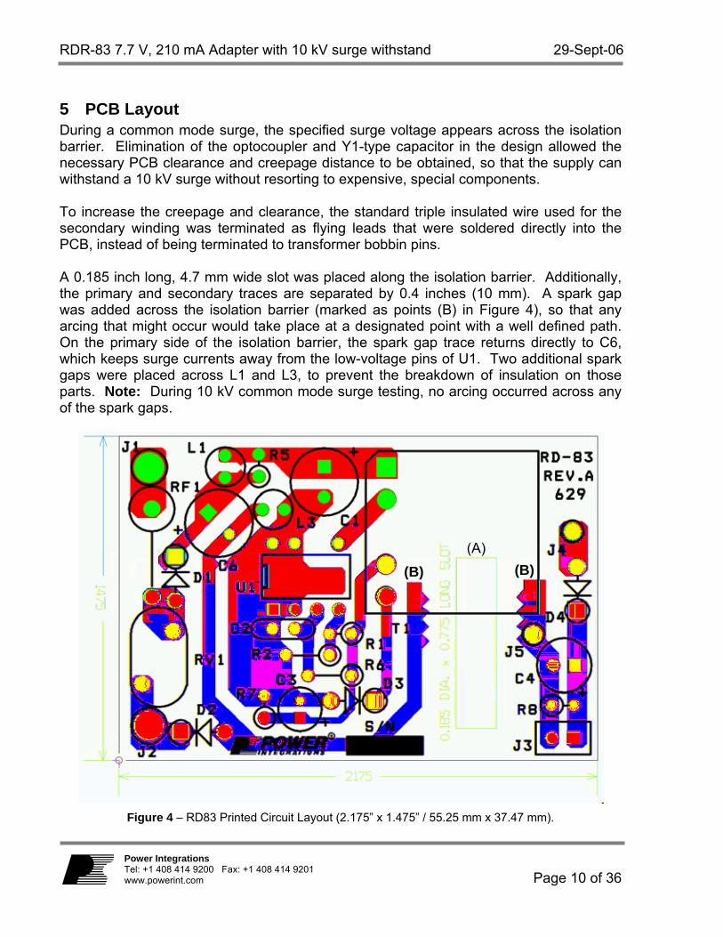
5 PCB Layout During a common mode surge, the specified surge voltage appears across the isolation barrier. Elimination of the optocoupler and Y1-type capacitor in the design allowed the necessary PCB clearance and creepage distance to be obtained, so that the supply can withstand a 10 kV surge without resorting to expensive, special components. To increase the creepage and clearance, the standard triple insulated wire used for the secondary winding was terminated as flying leads that were soldered directly into the PCB, instead of being terminated to transformer bobbin pins. A 0.185 inch long, 4.7 mm wide slot was placed along the isolation barrier. Additionally, the primary and secondary traces are separated by 0.4 inches (10 mm). A spark gap was added across the isolation barrier (marked as points (B) in Figure 4), so that any arcing that might occur would take place at a designated point with a well defined path. On the primary side of the isolation barrier, the spark gap trace returns directly to C6, which keeps surge currents away from the low-voltage pins of U1. Two additional spark gaps were placed across L1 and L3, to prevent the breakdown of insulation on those parts. Note: During 10 kV common mode surge testing, no arcing occurred across any of the spark gaps.
Figure 4 – RD83 Printed Circuit Layout (2.175” x 1.475” / 55.25 mm x 37.47 mm).
(A) (B) (B)
29-Sept-06 RDR-83 7.7 V, 210 mA Adapter with 10 kV surge withstand
Page 11 of 36
Power IntegrationsTel: +1 408 414 9200 Fax: +1 408 414 9201
www.powerint.com
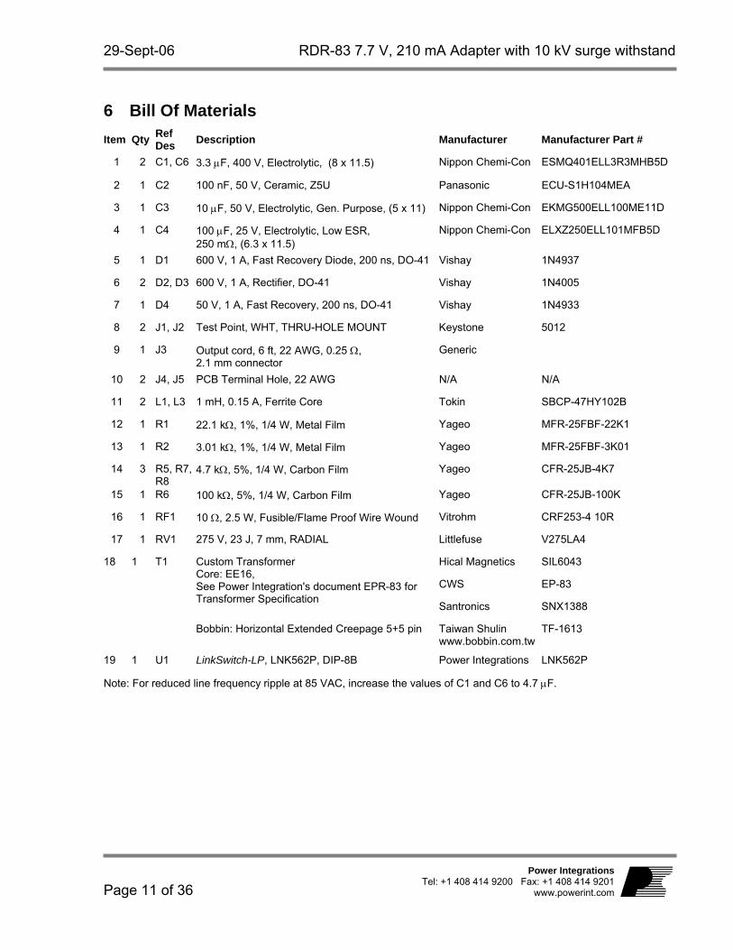
6 Bill Of Materials Item Qty Ref
Des Description Manufacturer Manufacturer Part #
1 2 C1, C6 3.3 µF, 400 V, Electrolytic, (8 x 11.5) Nippon Chemi-Con ESMQ401ELL3R3MHB5D
2 1 C2 100 nF, 50 V, Ceramic, Z5U Panasonic ECU-S1H104MEA
3 1 C3 10 µF, 50 V, Electrolytic, Gen. Purpose, (5 x 11) Nippon Chemi-Con EKMG500ELL100ME11D
4 1 C4 100 µF, 25 V, Electrolytic, Low ESR, 250 mΩ, (6.3 x 11.5)
Nippon Chemi-Con ELXZ250ELL101MFB5D
5 1 D1 600 V, 1 A, Fast Recovery Diode, 200 ns, DO-41 Vishay 1N4937
6 2 D2, D3 600 V, 1 A, Rectifier, DO-41 Vishay 1N4005
7 1 D4 50 V, 1 A, Fast Recovery, 200 ns, DO-41 Vishay 1N4933
8 2 J1, J2 Test Point, WHT, THRU-HOLE MOUNT Keystone 5012
9 1 J3 Output cord, 6 ft, 22 AWG, 0.25 Ω, 2.1 mm connector
Generic
10 2 J4, J5 PCB Terminal Hole, 22 AWG N/A N/A
11 2 L1, L3 1 mH, 0.15 A, Ferrite Core Tokin SBCP-47HY102B
12 1 R1 22.1 kΩ, 1%, 1/4 W, Metal Film Yageo MFR-25FBF-22K1
13 1 R2 3.01 kΩ, 1%, 1/4 W, Metal Film Yageo MFR-25FBF-3K01
14 3 R5, R7, R8
4.7 kΩ, 5%, 1/4 W, Carbon Film Yageo CFR-25JB-4K7
15 1 R6 100 kΩ, 5%, 1/4 W, Carbon Film Yageo CFR-25JB-100K
16 1 RF1 10 Ω, 2.5 W, Fusible/Flame Proof Wire Wound Vitrohm CRF253-4 10R
17 1 RV1 275 V, 23 J, 7 mm, RADIAL Littlefuse V275LA4
Hical Magnetics SIL6043
CWS EP-83
Custom Transformer Core: EE16, See Power Integration's document EPR-83 for Transformer Specification
Santronics SNX1388
18 1 T1
Bobbin: Horizontal Extended Creepage 5+5 pin Taiwan Shulin www.bobbin.com.tw
TF-1613
19 1 U1 LinkSwitch-LP, LNK562P, DIP-8B Power Integrations LNK562P
Note: For reduced line frequency ripple at 85 VAC, increase the values of C1 and C6 to 4.7 µF.

RDR-83 7.7 V, 210 mA Adapter with 10 kV surge withstand 29-Sept-06
Page 12 of 36
Power Integrations Tel: +1 408 414 9200 Fax: +1 408 414 9201www.powerint.com
7 Transformer Specification
7.1 Electrical Diagram
Bias/Core Cancellation
Primary
Secondary
3
42
1
FL
NC
1
FL
Shield176T #37AWG
3 LAYERS
29T #37AWG X 2 1 LAYER
17T #30AWG TIW
15T#32 AWG X 2
WD #1
WD #2
WD #4
WD #3
Figure 5 –Transformer Electrical Diagram.
7.2 Electrical Specifications
Electrical Strength 1 second, 60 Hz, from Pins 1-4 to Flying leads 6000 VAC
Primary Inductance Pins 1-2, all other windings open, measured at 100 kHz, 0.4 VRMS 3.5 mH, ±10%
Resonant Frequency Pins 1-2, all other windings open 250 kHz (Min.)
Primary Leakage Inductance Pins 1-2, with flying leads shorted, measured at 100 kHz, 0.4 VRMS 115 µH (Max.)
7.3 Materials Item Description [1] Core: PC40EE16-Z, TDK or equivalent gapped for AL of 114 nH/T2. Gap approx. 0.2 mm. [2] Bobbin: EE16 Horizontal 10 pin Taiwan Shulin TF-1613 or equivalent [3] Magnet Wire: #37 AWG [4] Magnet Wire: #32 AWG [5] Triple Insulated Wire: #30 AWG [6] Tape, 3M 1298 Polyester Film, 2.0 Mils thick, 8 mm wide [7] Varnish

29-Sept-06 RDR-83 7.7 V, 210 mA Adapter with 10 kV surge withstand
Page 13 of 36
Power IntegrationsTel: +1 408 414 9200 Fax: +1 408 414 9201
www.powerint.com
7.4 Transformer Build Diagram
Pin 3Pin 2
Pin 4
FLYING LEAD (MARKED)
Tape
Tape
WD #1Cancellation
WD #2PrimaryWD #3ShieldWD #4SecondaryTape
Pin 1NCPin 1FLYING LEADTape F i g u r e 6 – Transformer Build Diagram. 75 Transformer Construction Bobbin orientation is such that primary pins are on the left hand side of the winding spindle WD1 Cancellation and Bias Winding
Primary pin side of the bobbin oriented to the left hand side. Temporarily start at pin 7. Wind 29 bifilar turns of item [3] from right to left. Wind with tight tension evenly across the bobbin. Terminate finish on pin 4. Take t h e e n d o f t h e w i n d i n g t h a t w a s s t a r t e d o n p i n 7 a n d t e r m i n a t e i t o n p i n 3 .
Insulation 1 Layer of tape [6] for ins ulation. WD #2 Primary Winding Start at Pin 2. Wind 585turns of item [3] from left to right. Then wind 59
turns on the next layer from right to left. Wind 59 turns from left to right on the third layer. Wind with tight tension evenly across the bobbin. Bring the wire across the bobbin and terminate the finish on pin 1.
Insulation Use one layer of tape [6] for basic insulation. WD #3 Shield Winding
Temporarily start at Pin 7. Wind 15 bifilar turns of item [4]. Wind from right to left with tight tens ion ac ross t h e e n t i r e b o b b i n w i d t h . T e r m i n a t e o n pin 1. Cut the wire from Pin 7 and leave it unconnected.
Insulation Use three layers of tape [6] for bas ic insulation. WD #4 S e c o n d a r y W i n d i n g Temporarily start at Pin 7 (allow 1” of wire at the start for the flying lead). Wind 17 turns of item [5] from right to left with tight tens ion. Allow 1” of wire at the finish for the flying lead, at the right side of bobbin. Remove the start from pin 7 and mark. Exit sta r t a t r i g h t h a n d s i d e o f t h e b o b b i n . Outer insulation Wrap windings with three layers of tape [6]. Gap Core Gap core such that the inductanc e between pins 1 & 2 is 3.5 mH ±10%. The gap is approximately 0.2 mm. Core Assembly and trim fl ying leads Assemble and secure the core halves. Trim flying leads to 0.65”±0.05”. T i n l e a d s 0 . 1 5 ” ± 0 . 0 5 ” . C u t b o b b i n p i n s 5 , 6 , 7 a n d 8 . Varnish Dip varnis h as sembly with item [7].

RDR-83 7.7 V, 210 mA Adapter with 10 kV surge withstand 29-Sept-06
Page 14 of 36
Power Integrations Tel: +1 408 414 9200 Fax: +1 408 414 9201www.powerint.com
8 Design Spreadsheets ACDC_LinkSwitch-LP_053106; Rev.1.12; Copyright Power Integrations 2006
INPUT INFO OUTPUT UNIT ACDC_LinkSwitch-LP_053106_Rev1-12.xls; LinkSwitch-LP Continuous/Discontinuous Flyback Transformer Design Spreadsheet
ENTER APPLICATION VARIABLES RDR-83
VACMIN 85 Volts Minimum AC Input Voltage VACMAX 265 Volts Maximum AC Input Voltage fL 50 Hertz AC Mains Frequency VO 7.70 Volts Output Voltage (main) measured at the end of
output cable (For CV/CC designs enter typical CV tolerance limit)
IO 0.21 Amps Power Supply Output Current (For CV/CC designs enter typical CC tolerance limit)
Constant Voltage / Constant Current Output
YES CVCC Volts Choose "YES" from the 'CV/CC output' drop down box at the top of this spreadsheet for approximate CV/CC output. Choose "NO" for CV only output
Output Cable Resistance 0.25 0.25 Ohms Enter the resistance of the output cable (if used) PO 1.63 Watts Output Power (VO x IO + dissipation in output
cable) Feedback Type BIAS Bias
WindingChoose 'BIAS' for Bias winding feedback and 'OPTO' for Optocoupler feedback from the 'Feedback Type' drop down box at the top of this spreadsheet
Add Bias Winding YES Yes Choose 'YES' in the 'Bias Winding' drop down box at the top of this spreadsheet to add a Bias winding. Choose 'NO' to continue design without a Bias winding. Addition of Bias winding can lower no load consumption
Clampless design YES Clampless
Choose 'YES' from the 'clampless Design' drop down box at the top of this spreadsheet for a clampless design. Choose 'NO' to add an external clamp circuit. Clampless design lowers the total cost of the power supply
n 0.65 0.65 Efficiency Estimate at output terminals. For CV only designs enter 0.7 if no better data available
Z 0.35 0.35 Loss Allocation Factor (Secondary side losses / Total losses)
tC 2.90 mSeconds Bridge Rectifier Conduction Time Estimate CIN 9.40 UFarads Input Capacitance Input Rectification Type H H Choose H for Half Wave Rectifier and F for Full
Wave Rectification from the 'Rectification' drop down box at the top of this spreadsheet
ENTER LinkSwitch-LP VARIABLES
LinkSwitch-LP LNK562 LinkSwitch-LP device
Chosen Device LNK562 ILIMITMIN 0.124 Amps Minimum Current Limit ILIMITMAX 0.146 Amps Maximum Current Limit fSmin 61000 Hertz Minimum Device Switching Frequency

29-Sept-06 RDR-83 7.7 V, 210 mA Adapter with 10 kV surge withstand
Page 15 of 36
Power IntegrationsTel: +1 408 414 9200 Fax: +1 408 414 9201
www.powerint.com
I^2fMIN 1099 A^2Hz I^2f Minimum value (product of current limit squared and frequency is trimmed for tighter -tolerance)
I^2fTYP 1221 A^2Hz I^2f typical value (product of current limit squared and frequency is trimmed for tighter tolerance)
VOR 90.00 90 Volts Reflected Output Voltage VDS 10 Volts LinkSwitch-LP on-state Drain to Source Voltage VD 0.90 0.9 Volts Output Winding Diode Forward Voltage Drop KP 1.99 Ripple to Peak Current Ratio (0.9<KRP<1.0 :
1.0<KDP<6.0)
ENTER TRANSFORMER CORE/CONSTRUCTION VARIABLES
Core Type EE16 EE16 User-Selected transformer core
Core EE16 P/N: PC40EE16-Z Bobbin EE16_B
OBBIN P/N: EE16_BOBBIN
AE 0.192 cm^2 Core Effective Cross Sectional Area LE 3.5 cm Core Effective Path Length AL 1140 nH/T^2 Ungapped Core Effective Inductance BW 8.6 mm Bobbin Physical Winding Width M 0 mm Safety Margin Width (Half the Primary to
Secondary Creepage Distance) L 2 Number of primary layers NS 17 Number of Secondary Turns NB 44 Number of Bias winding turns VB 22.26 Volts Bias Winding Voltage R1 37.47 k-ohms Resistor divider component between bias
wiinding and FB pin of LinkSwitch-LP R2 3.00 k-ohms Resistor divider component between FB pin of
LinkSwitch-LP and primary RTN Recommended Bias Diode 1N4003 Place this diode on the return leg of the bias
winding for optimal EMI. See LinkSwitch-LP Design guide for more information
DC INPUT VOLTAGE PARAMETERS
VMIN 73 Volts Minimum DC Input Voltage VMAX 375 Volts Maximum DC Input Voltage
CURRENT WAVEFORM SHAPE PARAMETERS
DMAX 0.45 Maximum Duty Cycle IAVG 0.04 Amps Average Primary Current IP 0.12 Amps Minimum Peak Primary Current IR 0.12 Amps Primary Ripple Current IRMS 0.05 Amps Primary RMS Current
TRANSFORMER PRIMARY DESIGN PARAMETERS
LP 3486 uHenries Typical Primary Inductance. +/- 10%
LP_TOLERANCE 10 % Primary inductance tolerance

RDR-83 7.7 V, 210 mA Adapter with 10 kV surge withstand 29-Sept-06
Page 16 of 36
Power Integrations Tel: +1 408 414 9200 Fax: +1 408 414 9201www.powerint.com
NP 178 Primary Winding Number of Turns ALG 110 nH/T^2 Gapped Core Effective Inductance BM 1490 Gauss Maximum Operating Flux Density, BM<1500 is
recommended BAC 745 Gauss AC Flux Density for Core Loss Curves (0.5 X
Peak to Peak) ur 1654 Relative Permeability of Ungapped Core LG 0.20 Mm Gap Length (Lg > 0.1 mm) BWE 17.2 Mm Effective Bobbin Width OD 0.10 Mm Maximum Primary Wire Diameter including
insulation INS 0.02 Mm Estimated Total Insulation Thickness (= 2 * film
thickness) DIA 0.07 Mm Bare conductor diameter AWG 41 AWG Primary Wire Gauge (Rounded to next smaller
standard AWG value) CM 8 Cmils Bare conductor effective area in circular mils CMA 150 Cmils/Amp Primary Winding Current Capacity (150 < CMA <
500)
TRANSFORMER SECONDARY DESIGN PARAMETERS
Lumped parameters
ISP 1.30 Amps Peak Secondary Current ISRMS 0.47 Amps Secondary RMS Current IRIPPLE 0.42 Amps Output Capacitor RMS Ripple Current CMS 93 Cmils Secondary Bare Conductor minimum circular
mils AWGS 30 AWG Secondary Wire Gauge (Rounded up to next
larger standard AWG value) DIAS 0.26 Mm Secondary Minimum Bare Conductor Diameter ODS 0.51 Mm Secondary Maximum Outside Diameter for Triple
Insulated Wire INSS 0.12 Mm Maximum Secondary Insulation Wall Thickness
VOLTAGE STRESS PARAMETERS
VDRAIN - Volts Peak Drain Voltage is highly dependent on Transformer capacitance and leakage inductance. Please verify this on the bench and ensure that it is below 650 V to allow 50 V margin for transformer variation.
PIVS 44 Volts Output Rectifier Maximum Peak Inverse Voltage
TRANSFORMER SECONDARY DESIGN PARAMETERS (MULTIPLE OUTPUTS)
1st output
VO1 7.7 Volts Main Output Voltage (if unused, defaults to single output design)
IO1 0.211 Amps Output DC Current PO1 1.63 Watts Output Power VD1 0.9 Volts Output Diode Forward Voltage Drop NS1 17.00 Output Winding Number of Turns

29-Sept-06 RDR-83 7.7 V, 210 mA Adapter with 10 kV surge withstand
Page 17 of 36
Power IntegrationsTel: +1 408 414 9200 Fax: +1 408 414 9201
www.powerint.com
ISRMS1 0.470 Amps Output Winding RMS Current IRIPPLE1 0.42 Amps Output Capacitor RMS Ripple Current PIVS1 44 Volts Output Rectifier Maximum Peak Inverse Voltage Recommended Diodes SB160,
11DQ06Recommended Diodes for this output
Pre-Load Resistor 3 k-Ohms Recommended value of pre-load resistor CMS1 94 Cmils Output Winding Bare Conductor minimum
circular mils AWGS1 30 AWG Wire Gauge (Rounded up to next larger standard
AWG value) DIAS1 0.26 mm Minimum Bare Conductor Diameter ODS1 0.51 mm Maximum Outside Diameter for Triple Insulated
Wire
2nd output
VO2 Volts Output Voltage IO2 Amps Output DC Current PO2 0.00 Watts Output Power VD2 0.7 Volts Output Diode Forward Voltage Drop NS2 1.38 Output Winding Number of Turns ISRMS2 0.000 Amps Output Winding RMS Current IRIPPLE2 0.00 Amps Output Capacitor RMS Ripple Current PIVS2 3 Volts Output Rectifier Maximum Peak Inverse Voltage Recommended Diode Recommended Diodes for this output CMS2 0 Cmils Output Winding Bare Conductor minimum
circular mils AWGS2 AWG Wire Gauge (Rounded up to next larger standard
AWG value) DIAS2 mm Minimum Bare Conductor Diameter ODS2 mm Maximum Outside Diameter for Triple Insulated
Wire
3rd output
VO3 Volts Output Voltage IO3 Amps Output DC Current PO3 0.00 Watts Output Power VD3 0.7 Volts Output Diode Forward Voltage Drop NS3 1.38 Output Winding Number of Turns ISRMS3 0.000 Amps Output Winding RMS Current IRIPPLE3 0.00 Amps Output Capacitor RMS Ripple Current PIVS3 3 Volts Output Rectifier Maximum Peak Inverse Voltage Recommended Diode Recommended Diodes for this output CMS3 0 Cmils Output Winding Bare Conductor minimum
circular mils AWGS3 AWG Wire Gauge (Rounded up to next larger standard
AWG value) DIAS3 mm Minimum Bare Conductor Diameter ODS3 mm Maximum Outside Diameter for Triple Insulated
Wire

RDR-83 7.7 V, 210 mA Adapter with 10 kV surge withstand 29-Sept-06
Page 18 of 36
Power Integrations Tel: +1 408 414 9200 Fax: +1 408 414 9201www.powerint.com
Total power 1.63 Watts Total Output Power
Negative Output N/A If negative output exists enter Output number; eg: If VO2 is negative output, enter 2

29-Sept-06 RDR-83 7.7 V, 210 mA Adapter with 10 kV surge withstand
Page 19 of 36
Power IntegrationsTel: +1 408 414 9200 Fax: +1 408 414 9201
www.powerint.com
9 Performance Data All measurements performed at room temperature, 60 Hz input frequency.
9.1 Efficiency
Figure 7 – Efficiency vs. Input Voltage, Room Temperature, 60 Hz.
30
40
50
60
70
80
90
50 75 100 125 150 175 200 225 250 275 300
AC Input Voltage (V)
Effic
ienc
y (%
)
RDR-83 7.7 V, 210 mA Adapter with 10 kV surge withstand 29-Sept-06
Page 20 of 36
Power Integrations Tel: +1 408 414 9200 Fax: +1 408 414 9201www.powerint.com
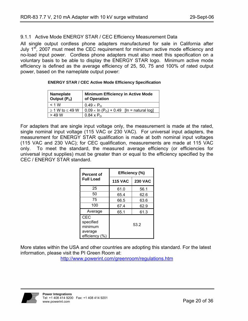
9.1.1 Active Mode ENERGY STAR / CEC Efficiency Measurement Data All single output cordless phone adapters manufactured for sale in California after July 1st, 2007 must meet the CEC requirement for minimum active mode efficiency and no-load input power. Cordless phone adapters must also meet this specification on a voluntary basis to be able to display the ENERGY STAR logo. Minimum active mode efficiency is defined as the average efficiency of 25, 50, 75 and 100% of rated output power, based on the nameplate output power:
ENERGY STAR / CEC Active Mode Efficiency Specification
Nameplate Output (PO)
Minimum Efficiency in Active Mode of Operation
< 1 W 0.49 × PO ≥ 1 W to ≤ 49 W 0.09 × ln (PO) + 0.49 [ln = natural log] > 49 W 0.84 x PO
For adapters that are single input voltage only, the measurement is made at the rated, single nominal input voltage (115 VAC or 230 VAC). For universal input adapters, the measurement for ENERGY STAR qualification is made at both nominal input voltages (115 VAC and 230 VAC); for CEC qualification, measurements are made at 115 VAC only. To meet the standard, the measured average efficiency (or efficiencies for universal input supplies) must be greater than or equal to the efficiency specified by the CEC / ENERGY STAR standard.
Efficiency (%) Percent of Full Load 115 VAC 230 VAC
25 61.0 56.1 50 65.4 62.6 75 66.5 63.6 100 67.4 62.9
Average 65.1 61.3 CEC specified minimum average efficiency (%)
53.2
More states within the USA and other countries are adopting this standard. For the latest information, please visit the PI Green Room at:
http://www.powerint.com/greenroom/regulations.htm

29-Sept-06 RDR-83 7.7 V, 210 mA Adapter with 10 kV surge withstand
Page 21 of 36
Power IntegrationsTel: +1 408 414 9200 Fax: +1 408 414 9201
www.powerint.com
9.2 No-load Input Power The supply easily meets the ENERGY STAR / CEC and European no-load power consumption specifications of 0.5 W and 0.3 W (respectively).
Figure 8 – No Load Input Power vs. Input Line Voltage, Room Temperature, 60 Hz.
9.3 Available Standby Output Power The supply provides >500 mW of available output power, at an input power of 1 W.
Figure 9 – Available Output Power at 1 Watt Input Power vs. Input Voltage.
0
0.05
0.1
0.15
0.2
0.25
0.3
0 50 100 150 200 250 300
AC Input Voltage (V)
Inpu
t Pow
er (W
)
0
0.1
0.2
0.3
0.4
0.5
0.6
0.7
0.8
0.9
1
0 50 100 150 200 250 300
AC Input Voltage (V)
Ava
ilabl
e O
utpu
t Pow
er (W
)

RDR-83 7.7 V, 210 mA Adapter with 10 kV surge withstand 29-Sept-06
Page 22 of 36
Power Integrations Tel: +1 408 414 9200 Fax: +1 408 414 9201www.powerint.com
9.4 Regulation
9.4.1 VI Curve vs. Input Voltage
Figure 10 – Output VI Curve, Room Temperature.
0
2
4
6
8
10
12
0 0.1 0.2 0.3 0.4 0.5 0.6 0.7 0.8Output Current (A)
Out
put V
olta
ge (V
)
LOWER LIMITUPPER LIMIT115 VAC85 VAC230 VAC265 VAC

RDR-83 7.7 V, 210 mA Adapter with 10 kV surge withstand 29-Sept-06
Page 24 of 36
Power Integrations Tel: +1 408 414 9200 Fax: +1 408 414 9201www.powerint.com
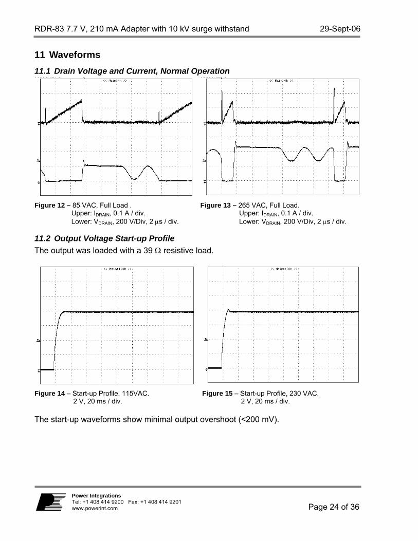
11 Waveforms 11.1 Drain Voltage and Current, Normal Operation
Figure 12 – 85 VAC, Full Load . Upper: IDRAIN, 0.1 A / div. Lower: VDRAIN, 200 V/Div, 2 µs / div.
Figure 13 – 265 VAC, Full Load. Upper: IDRAIN, 0.1 A / div. Lower: VDRAIN, 200 V/Div, 2 µs / div.
11.2 Output Voltage Start-up Profile The output was loaded with a 39 Ω resistive load.
Figure 14 – Start-up Profile, 115VAC. 2 V, 20 ms / div.
Figure 15 – Start-up Profile, 230 VAC. 2 V, 20 ms / div.
The start-up waveforms show minimal output overshoot (<200 mV).

29-Sept-06 RDR-83 7.7 V, 210 mA Adapter with 10 kV surge withstand
Page 25 of 36
Power IntegrationsTel: +1 408 414 9200 Fax: +1 408 414 9201
www.powerint.com
11.3 Drain Voltage and Current Start-up Profile The output was loaded with a 39 Ω resistive load and the output profile captured. These waveforms show no sign of core saturation and acceptable margin to the recommended maximum drain voltage of 650 VPK.
Figure 16 – 85 VAC Input and Maximum Load. Upper: IDRAIN, 0.1 A / div. Lower: VDRAIN, 100 V & 1 ms / div.
Figure 17 – 265 VAC Input and Maximum Load. Upper: IDRAIN, 0.1 A / div. Lower: VDRAIN, 200 V & 1 ms / div.

RDR-83 7.7 V, 210 mA Adapter with 10 kV surge withstand 29-Sept-06
Page 26 of 36
Power Integrations Tel: +1 408 414 9200 Fax: +1 408 414 9201www.powerint.com
11.4 Load Transient Response (50% to 100% Load Step) In the figures shown below, signal averaging was used to better enable viewing the load transient response. The oscilloscope was triggered using the load current step as a trigger source. Since the output switching and line frequency occur essentially at random with respect to the load transient, contributions to the output ripple from these sources will average out, leaving the contribution only from the load step response.
Figure 18 – Transient Response, 115 VAC, 50-100-50% Load Step. Top: Load Current, 0.1 A/div. Bottom: Output Voltage 200 mV, 500 µs / div.
Figure 19 – Transient Response, 230 VAC, 50-100-50% Load Step. Upper: Load Current, 0.1 A/ div. Bottom: Output Voltage 200 mV, 500 uS / div.
These results were significantly lower than the linear adapter where ripple and transient response variation was greater than 1 VP-P.

29-Sept-06 RDR-83 7.7 V, 210 mA Adapter with 10 kV surge withstand
Page 27 of 36
Power IntegrationsTel: +1 408 414 9200 Fax: +1 408 414 9201
www.powerint.com
11.5 Output Ripple Measurements
11.5.1 Ripple Measurement Technique For DC output ripple measurements, a modified oscilloscope test probe must be utilized in order to reduce the pickup of spurious signals. Details of the probe modification are provided in Figure 20 and Figure 21. The 5125BA probe adapter (from probe master) is affixed with two capacitors tied in parallel across the probe tip. The capacitors include one (1) 0.1 µF/50 V ceramic type and one (1) 1.0 µF/50 V aluminum electrolytic. The aluminum electrolytic type capacitor is polarized, so proper polarity across DC outputs must be maintained (see Figure 21).
Figure 20 – Oscilloscope Probe Prepared for Ripple Measurement (End Cap and Ground Lead Removed).
Figure 21 – Oscilloscope Probe with Probe Master 5125BA BNC Adapter (Modified with wires for probe
ground for ripple measurement, and two parallel decoupling capacitors added).
Probe Ground
Probe Tip

RDR-83 7.7 V, 210 mA Adapter with 10 kV surge withstand 29-Sept-06
Page 28 of 36
Power Integrations Tel: +1 408 414 9200 Fax: +1 408 414 9201www.powerint.com
11.5.2 Measurement Results
Figure 22 – Ripple, 85 VAC, Full Load.
5 ms, 50 mV / div (240 mVP-P). Figure 23 – Ripple, 115 VAC, Full Load.
5 ms, 50 mV / div (80 mVP-P).
Figure 24 – Ripple, 230 VAC, Full Load.
5 ms, 50 mV /div (130mVP-P). Figure 25 – Ripple of a Linear adaptor, 115 VAC
Input, Full Load. 2 ms, 200 mV/div (800 mVP-P).
Figure 22 shows increased line frequency ripple. If required, this could be lowered to the level shown in Figure 23 by increasing the value of C6 and C1 to 4.7 µF.

29-Sept-06 RDR-83 7.7 V, 210 mA Adapter with 10 kV surge withstand
Page 29 of 36
Power IntegrationsTel: +1 408 414 9200 Fax: +1 408 414 9201
www.powerint.com
12 Line Surge Differential and common mode 1.2/50 µs surge testing was completed on a single test unit, to IEC61000-4-5. Input voltage was set at 230 VAC / 60 Hz. The output of the supply was loaded to full load, and correct operation was verified following each surge event.
Surge Level (V)
Input Voltage (VAC)
Injection Location
Injection Phase (°)
Test Result (Pass/Fail)
+2000 230 L to N 90 Pass -2000 230 L to N 90 Pass
+10000 230 L,N to RTN 90 Pass -10000 230 L,N to RTN 90 Pass
Unit passed under all test conditions.

RDR-83 7.7 V, 210 mA Adapter with 10 kV surge withstand 29-Sept-06
Page 30 of 36
Power Integrations Tel: +1 408 414 9200 Fax: +1 408 414 9201www.powerint.com
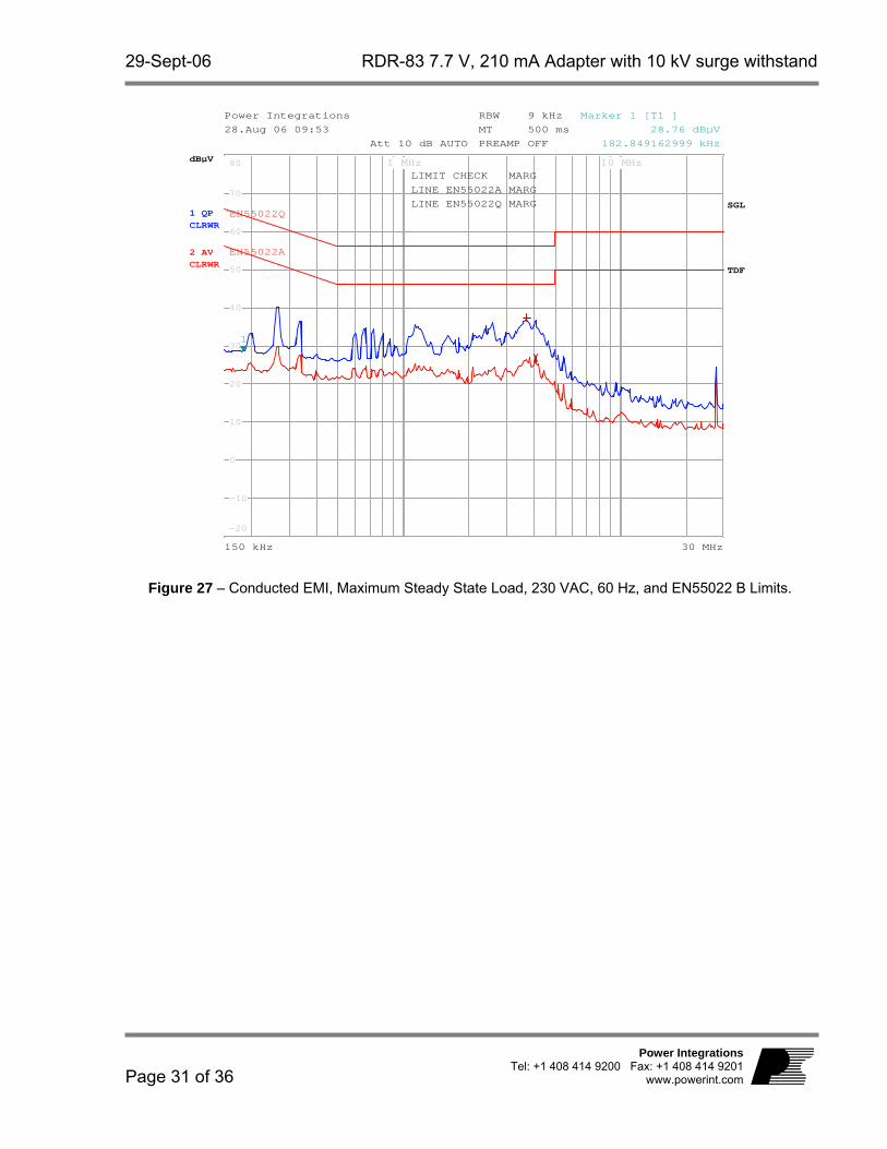
13 Conducted EMI Measurements were made with the output RTN of the supply connected to the artificial hand connection on the LISN (line impedance stabilization network) to represent worst-case conditions. The results show excellent margin of >15 dBµV to both the quasi-peak and the average limit lines.
Power Integrations
150 kHz 30 MHz
1 QPCLRWR
2 AVCLRWR
SGL
TDF
dBµV dBµV
RBW 9 kHzMT 500 msPREAMP OFFAtt 10 dB AUTO
28.Aug 06 09:43
1 MHz 10 MHz
-20
-10
0
10
20
30
40
50
60
70
80
LIMIT CHECK MARG
LINE EN55022A MARGLINE EN55022Q MARG
1
Marker 1 [T1 ] 28.50 dBµV 182.849162999 kHz
EN55022A
EN55022Q
Figure 26 – Conducted EMI, Maximum Steady State Load, 115 VAC, 60 Hz, and EN55022 B Limits.
29-Sept-06 RDR-83 7.7 V, 210 mA Adapter with 10 kV surge withstand
Page 31 of 36
Power IntegrationsTel: +1 408 414 9200 Fax: +1 408 414 9201
www.powerint.com
Power Integrations
150 kHz 30 MHz
1 QPCLRWR
2 AVCLRWR
SGL
TDF
dBµV dBµV
RBW 9 kHzMT 500 msPREAMP OFFAtt 10 dB AUTO
28.Aug 06 09:53
1 MHz 10 MHz
-20
-10
0
10
20
30
40
50
60
70
80LIMIT CHECK MARG
LINE EN55022A MARGLINE EN55022Q MARG
1
Marker 1 [T1 ] 28.76 dBµV 182.849162999 kHz
EN55022A
EN55022Q
Figure 27 – Conducted EMI, Maximum Steady State Load, 230 VAC, 60 Hz, and EN55022 B Limits.

RDR-83 7.7 V, 210 mA Adapter with 10 kV surge withstand 29-Sept-06
Page 32 of 36
Power Integrations Tel: +1 408 414 9200 Fax: +1 408 414 9201www.powerint.com
14 Revision History Date Author Revision Description & changes Reviewed 29-Sept-06 JAC 1.0 Initial Release PV, JJ, DA
29-Sept-06 RDR-83 7.7 V, 210 mA Adapter with 10 kV surge withstand
Page 33 of 36
Power IntegrationsTel: +1 408 414 9200 Fax: +1 408 414 9201
www.powerint.com
Notes

RDR-83 7.7 V, 210 mA Adapter with 10 kV surge withstand 29-Sept-06
Page 34 of 36
Power Integrations Tel: +1 408 414 9200 Fax: +1 408 414 9201www.powerint.com
Notes

29-Sept-06 RDR-83 7.7 V, 210 mA Adapter with 10 kV surge withstand
Page 35 of 36
Power IntegrationsTel: +1 408 414 9200 Fax: +1 408 414 9201
www.powerint.com
Notes

RDR-83 7.7 V, 210 mA Adapter with 10 kV surge withstand 29-Sept-06
Page 36 of 36
Power Integrations Tel: +1 408 414 9200 Fax: +1 408 414 9201www.powerint.com
For the latest updates, visit our website: www.powerint.com Power Integrations reserves the right to make changes to its products at any time to improve reliability or manufacturability. Power Integrations does not assume any liability arising from the use of any device or circuit described herein. POWER INTEGRATIONS MAKES NO WARRANTY HEREIN AND SPECIFICALLY DISCLAIMS ALL WARRANTIES INCLUDING, WITHOUT LIMITATION, THE IMPLIED WARRANTIES OF MERCHANTABILITY, FITNESS FOR A PARTICULAR PURPOSE, AND NON-INFRINGEMENT OF THIRD PARTY RIGHTS.
PATENT INFORMATION The products and applications illustrated herein (including transformer construction and circuits external to the products) may be covered by one or more U.S. and foreign patents, or potentially by pending U.S. and foreign patent applications assigned to Power Integrations. A complete list of Power Integrations’ patents may be found at www.powerint.com. Power Integrations grants its customers a license under certain patent rights as set forth at http://www.powerint.com/ip.htm. The PI Logo, TOPSwitch, TinySwitch, LinkSwitch, DPA-Switch, PeakSwitch, EcoSmart, Clampless, E-Shield, Filterfuse, PI Expert and PI FACTS are trademarks of Power Integrations, Inc. Other trademarks are property of their respective companies. ©Copyright 2006 Power Integrations, Inc.
Power Integrations Worldwide Sales Support Locations
WORLD HEADQUARTERS 5245 Hellyer Avenue San Jose, CA 95138, USA. Main: +1-408-414-9200 Customer Service: Phone: +1-408-414-9665 Fax: +1-408-414-9765 e-mail: [email protected]
GERMANY Rueckertstrasse 3 D-80336, Munich Germany Phone: +49-89-5527-3910 Fax: +49-89-5527-3920 e-mail: [email protected]
JAPAN Keihin Tatemono 1st Bldg 2-12-20 Shin-Yokohama, Kohoku-ku, Yokohama-shi, Kanagawa ken, Japan 222-0033 Phone: +81-45-471-1021 Fax: +81-45-471-3717 e-mail: [email protected]
TAIWAN 5F, No. 318, Nei Hu Rd., Sec. 1 Nei Hu Dist. Taipei, Taiwan 114, R.O.C. Phone: +886-2-2659-4570 Fax: +886-2-2659-4550 e-mail: [email protected]
CHINA (SHANGHAI) Rm 807-808A, Pacheer Commercial Centre, 555 Nanjing Rd. West Shanghai, P.R.C. 200041 Phone: +86-21-6215-5548 Fax: +86-21-6215-2468 e-mail: [email protected]
INDIA 261/A, Ground Floor 7th Main, 17th Cross, Sadashivanagar Bangalore, India 560080 Phone: +91-80-41138020 Fax: +91-80-41138023 e-mail: [email protected]
KOREA RM 602, 6FL Korea City Air Terminal B/D, 159-6 Samsung-Dong, Kangnam-Gu, Seoul, 135-728, Korea Phone: +82-2-2016-6610 Fax: +82-2-2016-6630 e-mail: [email protected]
UNITED KINGDOM 1st Floor, St. James’s House East Street, Farnham Surrey, GU9 7TJ United Kingdom Phone: +44 (0) 1252-730-140 Fax: +44 (0) 1252-727-689 e-mail: [email protected]
CHINA (SHENZHEN) Room 2206-2207, Block A, Elec. Sci. Tech. Bldg. 2070 Shennan Zhong Rd. Shenzhen, Guangdong, China, 518031 Phone: +86-755-8379-3243 Fax: +86-755-8379-5828 e-mail: [email protected]
ITALY Via De Amicis 2 20091 Bresso MI – Italy Phone: +39-028-928-6000 Fax: +39-028-928-6009 e-mail: [email protected]
SINGAPORE 51 Newton Road, #15-08/10 Goldhill Plaza, Singapore, 308900 Phone: +65-6358-2160 Fax: +65-6358-2015 e-mail: [email protected]
APPLICATIONS HOTLINE World Wide +1-408-414-9660 APPLICATIONS FAX World Wide +1-408-414-9760
Related Documents


![(Reference [2]) LINEAR PHASE LOCKED LOOPS - …users.ece.gatech.edu/.../ECE_6440/Summer_2003/L060-LPLL-II(2UP).pdf · (Reference [2]) LINEAR PHASE LOCKED LOOPS - CONTINUED THE ACQUISTION](https://static.cupdf.com/doc/110x72/5ad972fe7f8b9a52528b89b2/reference-2-linear-phase-locked-loops-usersece-2uppdfreference-2.jpg)


