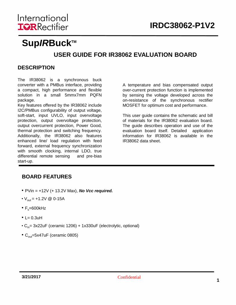
IRDC38062-P1V2 Confidential 3/21/2017 1 USER GUIDE FOR IR38062 EVALUATION BOARD DESCRIPTION The IR38062 is a synchronous buck converter with a PMBus interface, providing a compact, high performance and flexible solution in a small 5mmx7mm PQFN package. Key features offered by the IR38062 include I2C/PMBus configurability of output voltage, soft-start, input UVLO, input overvoltage protection, output overvoltage protection, output overcurrent protection, Power Good, thermal protection and switching frequency. Additionally, the IR38062 also features enhanced line/ load regulation with feed forward, external frequency synchronization with smooth clocking, internal LDO, true differential remote sensing and pre-bias start-up. A temperature and bias compensated output over-current protection function is implemented by sensing the voltage developed across the on-resistance of the synchronous rectifier MOSFET for optimum cost and performance. This user guide contains the schematic and bill of materials for the IR38062 evaluation board. The guide describes operation and use of the evaluation board itself. Detailed application information for IR38062 is available in the IR38062 data sheet. BOARD FEATURES • PVin = +12V (+ 13.2V Max), No Vcc required. • V out = +1.2V @ 0-15A • F s =600kHz • L= 0.3uH • C in = 3x22uF (ceramic 1206) + 1x330uF (electrolytic, optional) • C out =5x47uF (ceramic 0805) SupIRBuck TM

Welcome message from author
This document is posted to help you gain knowledge. Please leave a comment to let me know what you think about it! Share it to your friends and learn new things together.
Transcript
IRDC38062-P1V2
Confidential
3/21/2017 1
USER GUIDE FOR IR38062 EVALUATION BOARD
DESCRIPTION
The IR38062 is a synchronous buck
converter with a PMBus interface, providing
a compact, high performance and flexible
solution in a small 5mmx7mm PQFN
package.
Key features offered by the IR38062 include
I2C/PMBus configurability of output voltage,
soft-start, input UVLO, input overvoltage
protection, output overvoltage protection,
output overcurrent protection, Power Good,
thermal protection and switching frequency.
Additionally, the IR38062 also features
enhanced line/ load regulation with feed
forward, external frequency synchronization
with smooth clocking, internal LDO, true
differential remote sensing and pre-bias
start-up.
A temperature and bias compensated output
over-current protection function is implemented
by sensing the voltage developed across the
on-resistance of the synchronous rectifier
MOSFET for optimum cost and performance.
This user guide contains the schematic and bill
of materials for the IR38062 evaluation board.
The guide describes operation and use of the
evaluation board itself. Detailed application
information for IR38062 is available in the
IR38062 data sheet.
BOARD FEATURES
• PVin = +12V (+ 13.2V Max), No Vcc required.
• Vout = +1.2V @ 0-15A
• Fs=600kHz
• L= 0.3uH
• Cin= 3x22uF (ceramic 1206) + 1x330uF (electrolytic, optional)
• Cout=5x47uF (ceramic 0805)
SupIRBuckTM

IRDC38062-P1V2
Confidential
3/21/2017
2
A well regulated +12V input supply should be connected to PVin+ and PVin-. A maximum of 15A load should
be connected to VOUT+ and VOUT-. The inputs and output connections of the board are listed in Table I.
IR38062 needs only one input supply and internal LDO generates Vcc from PVin. Another internal LDo
generates the 1.8V needed by the internal digital circuits. If operation with external Vcc is required, then R25
should be removed and external Vcc can be applied between Vcc+ and Vcc- pins. Vin pin and Vcc pins
should be shorted together for external Vcc operation by installing R24. For normal, non-tracking
operation, R27 should not be populated and a 100 kOhm resistor should be connected from the
Track_En pin to P1V8.
The board is configured for remote sensing. If local sense is desired, R8 should be uninstalled and R16
should be installed instead.
I2C/PMBus communication is established through the 4 pin header which allows connection to the
SCL/SDA/SALERT and GND lines from the host/dongle. For proper operation in digital communications
mode, R35 must always be populated.
External Enable signal can be applied to the board via exposed Enable pad and R18 should be removed for
this purpose.
CONNECTIONS and OPERATING INSTRUCTIONS
LAYOUT The PCB is a 6-layer board. All of layers are 2 Oz. copper. The IR38062 and most of the passive
components are mounted on the top side of the board. Power supply decoupling capacitors and
feedback components are located close to IR38062. The feedback resistors are connected to the
output of the remote sense amplifier of the IR38062 and are located close to the IR38062. To improve
efficiency, the circuit board is designed to minimize the length of the on-board power ground current
path. Separate power ground and analog ground are used and may be connected together using a 0
ohm resistor.
Table I. Connections
Connection Signal Name
PVin+ PVin (+12V)
PVin- Ground of PVin
Vout+ Vout(+1.2V)
Vout- Ground for Vout
Vcc+ Vcc Pin
Vcc- Ground for Vcc input
Enable Enable
PGood Power Good Signal
IRDC38062-P1V2
Confidential
3/21/2017
3
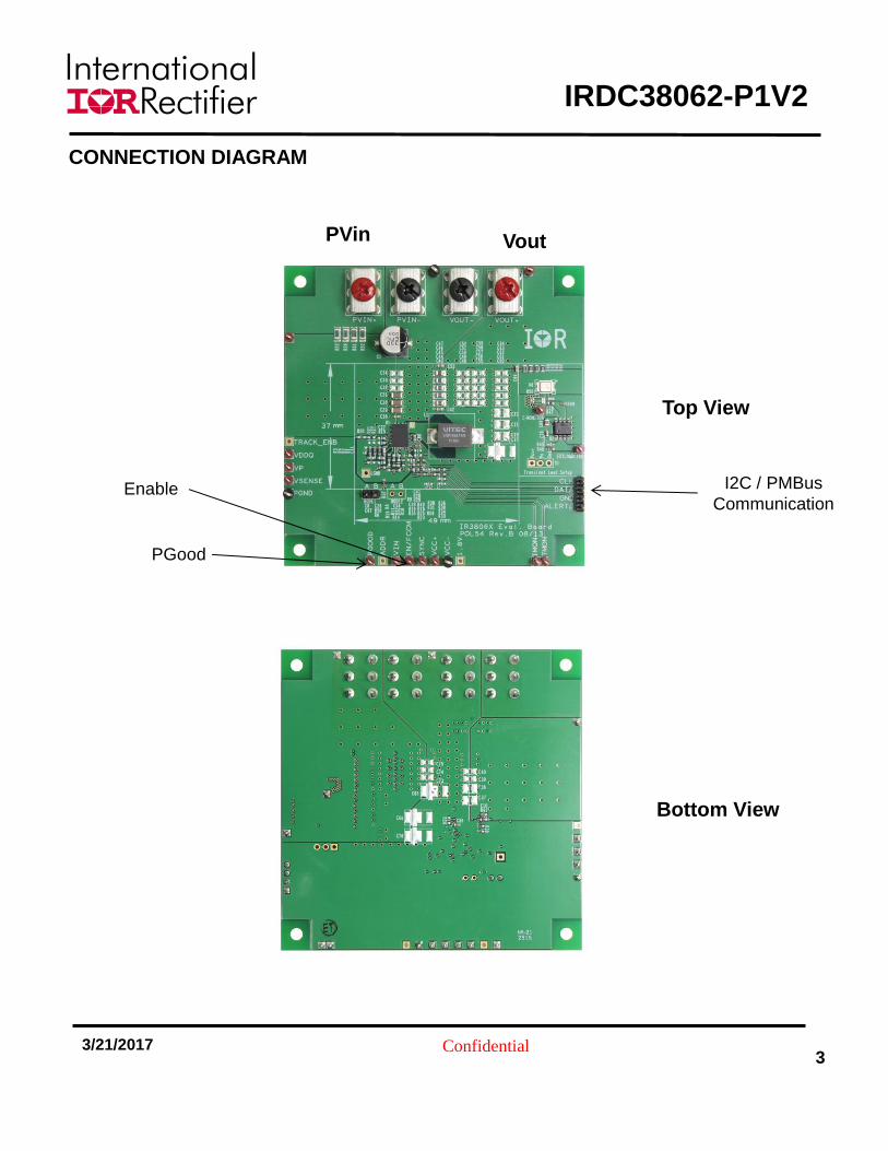
CONNECTION DIAGRAM
Top View
Bottom View
Vout PVin
PGood
Enable I2C / PMBus
Communication
IRDC38062-P1V2
Confidential
3/21/2017
4
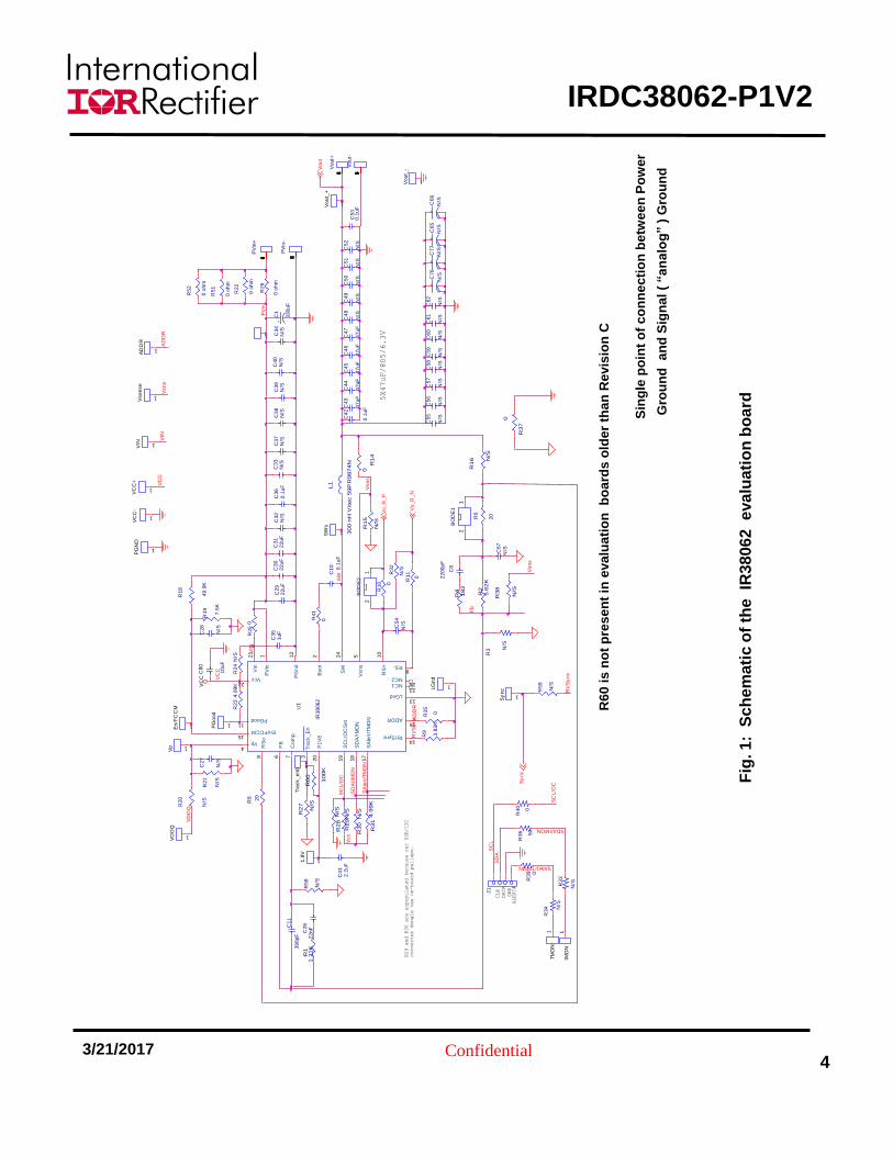
Fig
. 1:
Sc
he
ma
tic o
f th
e IR
38062
e
va
lua
tio
n b
oa
rd
S
ing
le p
oin
t o
f c
on
ne
cti
on
be
twe
en
Po
wer
G
rou
nd
a
nd
Sig
na
l ( “analog” )
Gro
un
d
R29N
/S
U1
IR3
8062
Vin
21
LGnd13
Rt/Sync14
Vcc22
Com
p7
Vsns
5
PG
nd
12
SC
L/O
CS
et
19
FB
6
Boot
2
PGood11
PV
in1
RS-9
RS
+10
RS
o8
SW
24
3Tra
ck_E
n
Vp4
En/FCCM15
SD
A/I
MO
N18
SA
lert
/TM
ON
17
ADDR16
P1V
820
NC123
NC226
R30
N/S
R25
0
R31
4.9
9K
En/F
CC
M
1
R8 20
SD
A/I
MO
N
VD
DQ
GND
SA
lert
/TM
ON
SD
A
SDA/IMON
CLK
DATA
J1
R40 0
R3
6 50
SC
L
VIN
R27
N/S
Vcc
R24
N/S
SC
L/O
C
C35
1uF
VC
C+
1
VC
C
VIN 1
Vsns
VIN
Vsense
1
VC
CC80
10uF
BO
DE
2
12
PG
ood
1
R23
4.9
9K
R51
0 o
hm
R52
0 o
hm
Vo
ut_
+
1
Vou
t_-
1
BO
DE
1
12
R39 0
ALERT#
VC
C-
1
R18
49.9
KR
19
7.5
K
C38
N/S
C28
N/S
C4
0N
/SC
39
N/S
R2
2
0 o
hm
R29 and R30 are unpopulated because our USB/I2C
converter dongle has on-board pullups.
R26
0 o
hm
PG
ND
1
C32
N/S
C29
22uF
C31
22uF
C30
22uF
C37
N/S
C10 0.1
uF
+C
1
330uF
PV
in-
123456
C36
0.1
uF
C34
N/S
C33
N/S
Vou
t-
123456
PV
in+
123456
Vo
ut+
123456
VC
C
IMO
N1
R33
N/S
TM
ON
1
SAlert/TMON
R34 N
/SS
CL
/OC
PV
in
Sy
nc
Rt/
Sy
nc
Sy
nc
1
R9
3.8
3K
R28
N/S
C61
N/S
C6
2
N/S
C53
0.1
uF
L1
300 n
H V
itec 5
9P
R9874N
R3
5
0
C54
N/S
R10 0
Fb
C67
N/S
C59
N/S
C60
N/S
C57
N/S
C5
8
N/S
R38
N/S
C56
N/S
C55
N/S
SW
s
1
SW
R16 N
/S
R4
182
R2
5.6
2K
C52
N/S
Vsns
R6
20
C5
1
N/S
C50
N/S
R58
N/S
C49
N/S
+C
76
N/S
C48
N/S
1.8
V
1
C4
7
47uF
Vsns
5X47uF/805/6.3V
R15
N/S
+C
77
N/S
+C
65
N/S
R41
0
+C
66
N/S
C46
47uF
C8
2200pF
R14
0
C4
5
47uF
R11
0
R32
N/S
C44
47uF
C43
47uF
Vo_R
_P
R37
0
Vo_R
_N
C42
0.1
uF
AD
DR
Rt/
Sy
nc
C41
2.2
uF
R60
100K
Vp 1
R20
N/S
R21
N/S
R3 N
/S
AD
DR
AD
DR
1
LG
nd
1
Vout
Tra
ck_en
b
1
C26
22nF
R1
1.2
1K
C11
390pF
R59
N/S
C27
N/S
1
VD
DQ
1
R
60
is
no
t p
res
en
t in
eva
lua
tio
n b
oa
rds
old
er
tha
n R
evis
ion
C
IRDC38062-P1V2
Confidential
3/21/2017 5
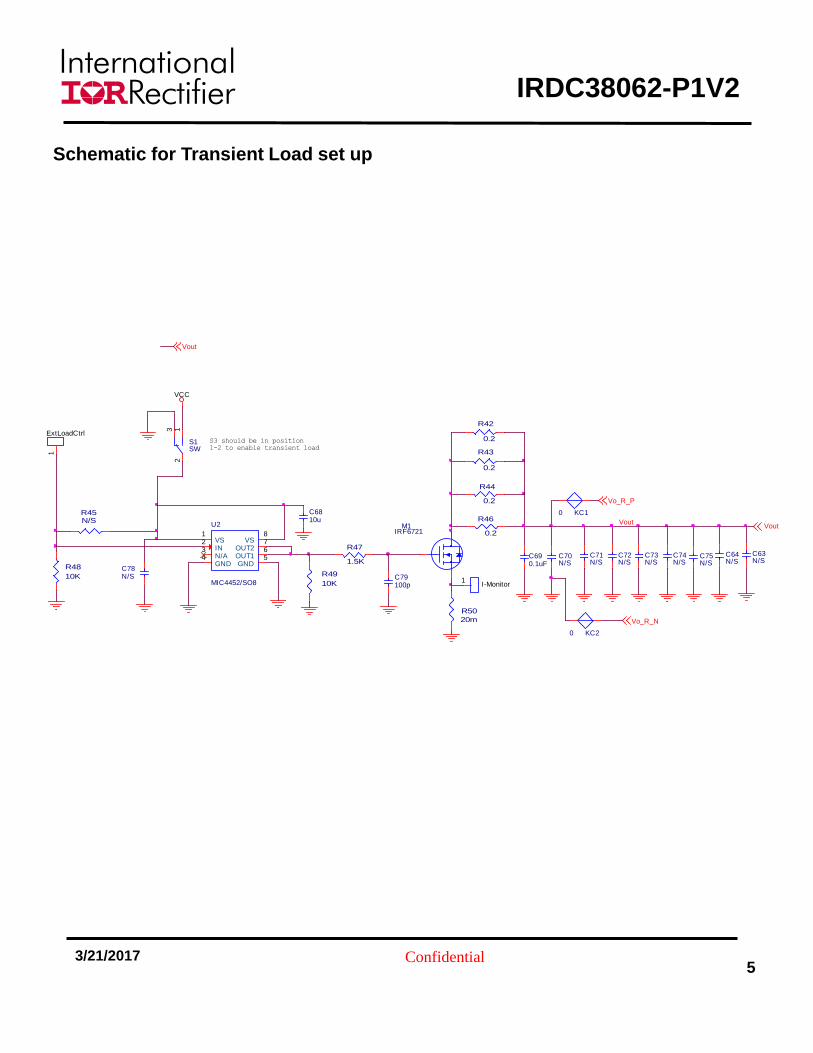
Schematic for Transient Load set up
Vout
S3 should be in position 1-2 to enable transient load
R50
20m
C75N/S
C71N/S
C70N/S
C64N/S
C6810u
R42
0.2
R43
0.2
R44
0.2
R46
0.2
R47
1.5K
ExtLoadCtrl
1
M1IRF6721
U2
MIC4452/SO8
VS1
IN2
GND4
GND5OUT16OUT27VS8
N/A3
R45N/S
R49
10K
S1SW
213
C690.1uF
C78N/S
R48
10K
Vout
C79100p
C63N/S
Vo_R_P
Vo_R_N
VCC
I-Monitor1
C72N/S
C73N/S
C74N/S
KC10
KC20
Vout
IRDC38062-P1V2
Confidential
3/21/2017 6
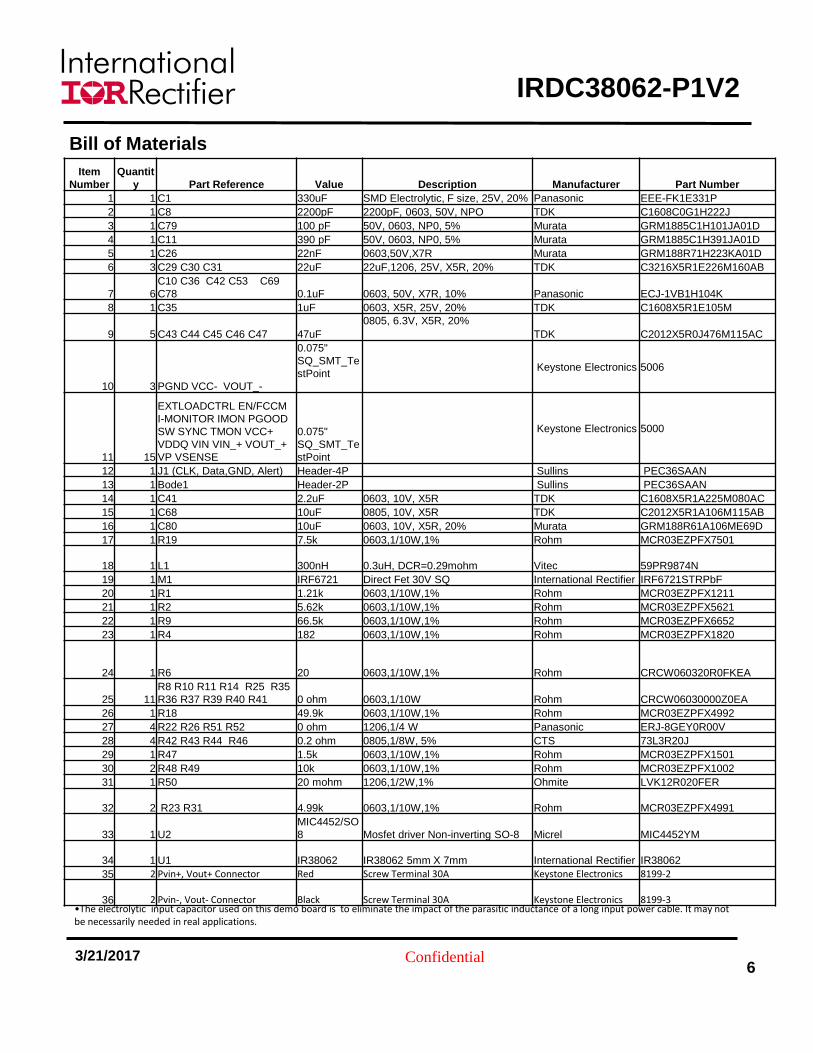
Bill of Materials
•The electrolytic input capacitor used on this demo board is to eliminate the impact of the parasitic inductance of a long input power cable. It may not be necessarily needed in real applications.
Item
Number
Quantit
y Part Reference Value Description Manufacturer Part Number
1 1 C1 330uF SMD Electrolytic, F size, 25V, 20% Panasonic EEE-FK1E331P
2 1 C8 2200pF 2200pF, 0603, 50V, NPO TDK C1608C0G1H222J
3 1 C79 100 pF 50V, 0603, NP0, 5% Murata GRM1885C1H101JA01D
4 1 C11 390 pF 50V, 0603, NP0, 5% Murata GRM1885C1H391JA01D
5 1 C26 22nF 0603,50V,X7R Murata GRM188R71H223KA01D
6 3 C29 C30 C31 22uF 22uF,1206, 25V, X5R, 20% TDK C3216X5R1E226M160AB
7 6
C10 C36 C42 C53 C69
C78 0.1uF 0603, 50V, X7R, 10% Panasonic ECJ-1VB1H104K
8 1 C35 1uF 0603, X5R, 25V, 20% TDK C1608X5R1E105M
9 5 C43 C44 C45 C46 C47 47uF
0805, 6.3V, X5R, 20%
TDK C2012X5R0J476M115AC
10 3 PGND VCC- VOUT_-
0.075"
SQ_SMT_Te
stPoint
Keystone Electronics 5006
11 15
EXTLOADCTRL EN/FCCM
I-MONITOR IMON PGOOD
SW SYNC TMON VCC+
VDDQ VIN VIN_+ VOUT_+
VP VSENSE
0.075"
SQ_SMT_Te
stPoint
Keystone Electronics 5000
12 1 J1 (CLK, Data,GND, Alert) Header-4P Sullins PEC36SAAN
13 1 Bode1 Header-2P Sullins PEC36SAAN
14 1 C41 2.2uF 0603, 10V, X5R TDK C1608X5R1A225M080AC
15 1 C68 10uF 0805, 10V, X5R TDK C2012X5R1A106M115AB
16 1 C80 10uF 0603, 10V, X5R, 20% Murata GRM188R61A106ME69D
17 1 R19 7.5k 0603,1/10W,1% Rohm MCR03EZPFX7501
18 1 L1 300nH 0.3uH, DCR=0.29mohm Vitec 59PR9874N
19 1 M1 IRF6721 Direct Fet 30V SQ International Rectifier IRF6721STRPbF
20 1 R1 1.21k 0603,1/10W,1% Rohm MCR03EZPFX1211
21 1 R2 5.62k 0603,1/10W,1% Rohm MCR03EZPFX5621
22 1 R9 66.5k 0603,1/10W,1% Rohm MCR03EZPFX6652
23 1 R4 182 0603,1/10W,1% Rohm MCR03EZPFX1820
24 1 R6 20 0603,1/10W,1% Rohm CRCW060320R0FKEA
25 11
R8 R10 R11 R14 R25 R35
R36 R37 R39 R40 R41 0 ohm 0603,1/10W Rohm CRCW06030000Z0EA
26 1 R18 49.9k 0603,1/10W,1% Rohm MCR03EZPFX4992
27 4 R22 R26 R51 R52 0 ohm 1206,1/4 W Panasonic ERJ-8GEY0R00V
28 4 R42 R43 R44 R46 0.2 ohm 0805,1/8W, 5% CTS 73L3R20J
29 1 R47 1.5k 0603,1/10W,1% Rohm MCR03EZPFX1501
30 2 R48 R49 10k 0603,1/10W,1% Rohm MCR03EZPFX1002
31 1 R50 20 mohm 1206,1/2W,1% Ohmite LVK12R020FER
32 2 R23 R31 4.99k 0603,1/10W,1% Rohm MCR03EZPFX4991
33 1 U2
MIC4452/SO
8 Mosfet driver Non-inverting SO-8 Micrel MIC4452YM
34 1 U1 IR38062 IR38062 5mm X 7mm International Rectifier IR38062
35 2 Pvin+, Vout+ Connector Red Screw Terminal 30A Keystone Electronics 8199-2
36 2 Pvin-, Vout- Connector Black Screw Terminal 30A Keystone Electronics 8199-3
IRDC38062-P1V2
Confidential
3/21/2017
7
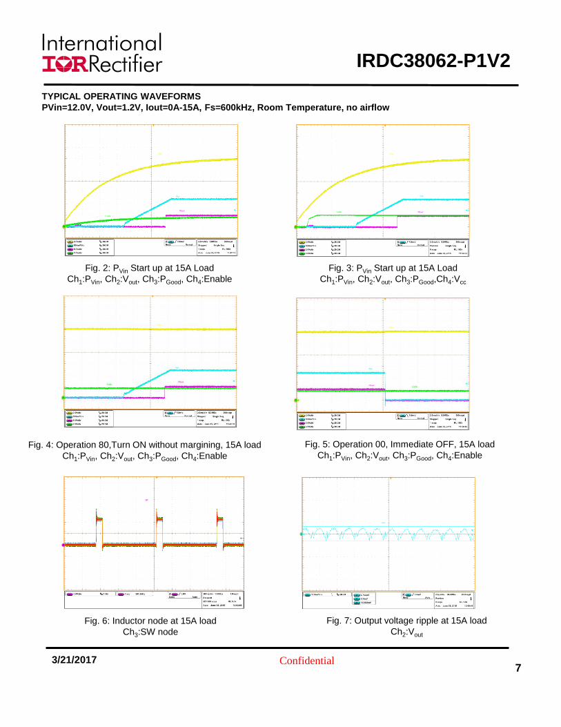
TYPICAL OPERATING WAVEFORMS
PVin=12.0V, Vout=1.2V, Iout=0A-15A, Fs=600kHz, Room Temperature, no airflow
Fig. 5: Operation 00, Immediate OFF, 15A load
Ch1:PVin, Ch2:Vout, Ch3:PGood, Ch4:Enable
Fig. 6: Inductor node at 15A load
Ch3:SW node
Fig. 3: PVin Start up at 15A Load
Ch1:PVin, Ch2:Vout, Ch3:PGood,Ch4:Vcc
Fig. 2: PVin Start up at 15A Load
Ch1:PVin, Ch2:Vout, Ch3:PGood, Ch4:Enable
Fig. 4: Operation 80,Turn ON without margining, 15A load
Ch1:PVin, Ch2:Vout, Ch3:PGood, Ch4:Enable
Fig. 7: Output voltage ripple at 15A load
Ch2:Vout

IRDC38062-P1V2
Confidential
3/21/2017
8
Fig. 9: Short-circuit recovery (Hiccup) at 15A load
Ch2:Vout, Ch3:PGood
Fig. 8: 0.35V Prebias voltage startup at 0A load
Ch2:Vout, Ch3:PGood
TYPICAL OPERATING WAVEFORMS
PVin=12.0V, Vout=1.2V, Iout=0A-15A, Fs=600kHz, Room Temperature, no airflow
IRDC38062-P1V2
Confidential
3/21/2017 9
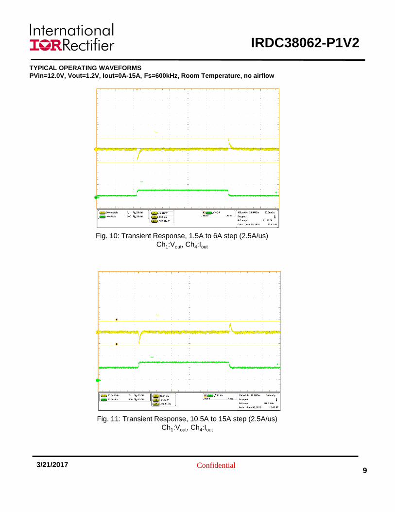
Fig. 10: Transient Response, 1.5A to 6A step (2.5A/us)
Ch1:Vout, Ch4:Iout
Fig. 11: Transient Response, 10.5A to 15A step (2.5A/us)
Ch1:Vout, Ch4:Iout
TYPICAL OPERATING WAVEFORMS
PVin=12.0V, Vout=1.2V, Iout=0A-15A, Fs=600kHz, Room Temperature, no airflow

IRDC38062-P1V2
Confidential
3/21/2017
10
Fig. 12: Bode Plot at 0A load
Bandwidth = 79.6kHz, Phase Margin = 59.5o , Gain Margin = 13.4dB
Fig. 13: Bode Plot at 15A load
Bandwidth = 79.6kHz, Phase Margin = 50.3o, Gain Margin = 13.4dB
TYPICAL OPERATING WAVEFORMS
PVin=12.0V, Vout=1.2V, Iout=0A-15A, Fs=600kHz, Room Temperature, no airflow

IRDC38062-P1V2
Confidential
3/21/2017
11
Fig15: Power loss versus load current
Fig.14: Efficiency versus load current
TYPICAL OPERATING WAVEFORMS
PVin=12.0V, Vout=1.2V, Iout=0A-15A, Fs=600kHz, Room Temperature, no airflow
IRDC38062-P1V2
Confidential
3/21/2017
12
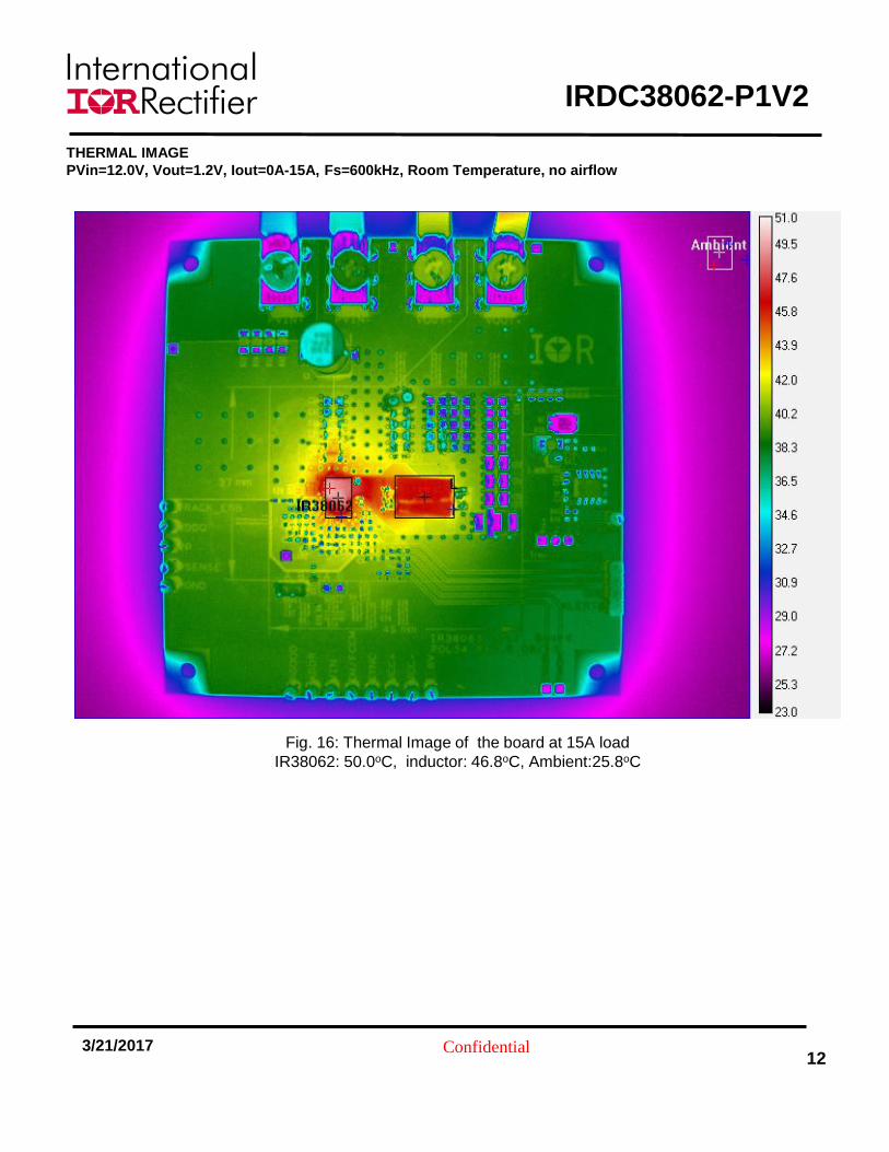
Fig. 16: Thermal Image of the board at 15A load
IR38062: 50.0oC, inductor: 46.8oC, Ambient:25.8oC
THERMAL IMAGE
PVin=12.0V, Vout=1.2V, Iout=0A-15A, Fs=600kHz, Room Temperature, no airflow

IRDC38062-P1V2
Confidential
3/21/2017
13
Fig. 17: PMBus Command Summary for the 1.2V design
PMBus Command Summary
PVin=12.0V, Vout=1.2V, Iout=0A-15A, Fs=600kHz,

IRDC38062-P1V2
Confidential
Quick Start: PowIRCenter GUI Connecting devices
14
Start PowIRCenter &
Connect USB Dongle Step 1
Step 2 Detect attached demoboards
USB Dongle connected
USB Dongle NOT detected
Press “Auto Populate Devices” button to detect boards connected to USB dongle
IRDC38062-P1V2
Confidential
15
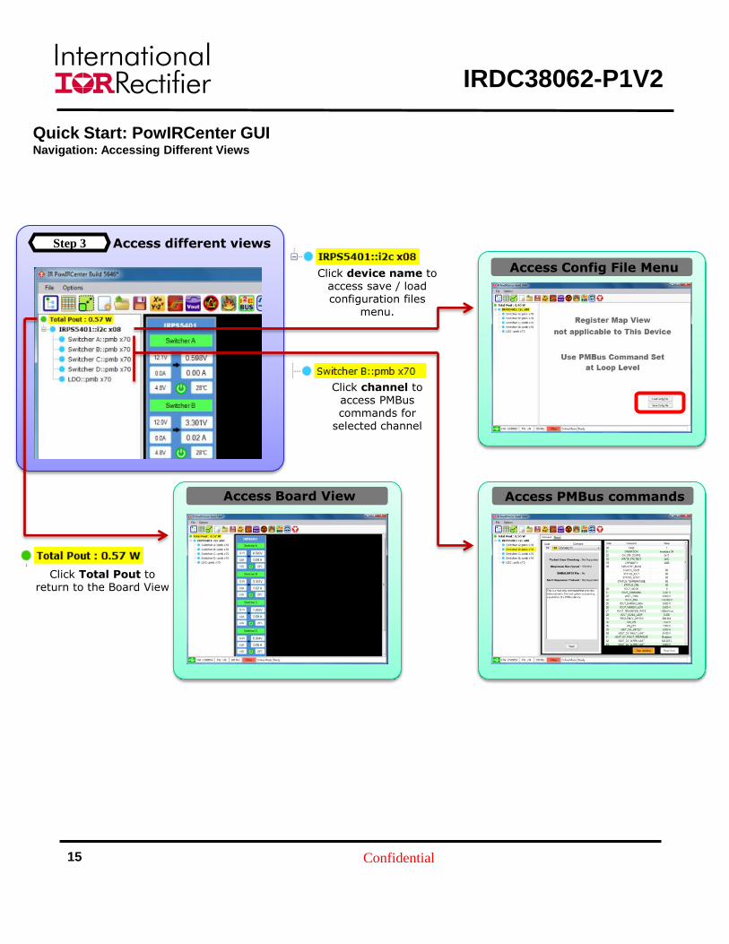
Step 3 Access different views
Click device name to access save / load configuration files
menu.
Access Board View
Click Total Pout to return to the Board View
Access PMBus commands
Click channel to access PMBus commands for
selected channel
Access Config File Menu
Quick Start: PowIRCenter GUI Navigation: Accessing Different Views
IRDC38062-P1V2
Confidential
16
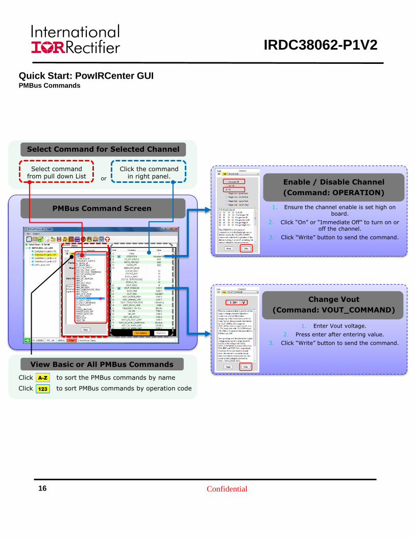
Click the command in right panel.
Enable / Disable Channel
(Command: OPERATION)
Change Vout
(Command: VOUT_COMMAND)
1. Enter Vout voltage.
2. Press enter after entering value.
3. Click “Write” button to send the command.
1. Ensure the channel enable is set high on board.
2. Click “On” or “Immediate Off” to turn on or off the channel.
3. Click “Write” button to send the command.
PMBus Command Screen
*
*
Select command from pull down List
Select Command for Selected Channel
or
*
Click to sort the PMBus commands by name
Click to sort PMBus commands by operation code
View Basic or All PMBus Commands
Quick Start: PowIRCenter GUI PMBus Commands
Related Documents