Authorized licenseduse limitedto: Universityof Michigan Library. Downloaded on December 28,2020 at 00:23:48 UTC from IEEE Xplore. Restlictions apply. Milad Zolfagharlo o Koohi and Amir Mor t azawi ireless communication has become an integra l part of our lives, continuously improving the qualityofour everyday activities. A multitude of functionalities are offered by recent generations of mobile phones, resulting in a significant adop- tion of wireless devices and a growth in data traffic,as reported by Ericsson [1] in Figure 1. To accommodate consumers' continuous demands for high data rates, the number of frequency bands allo- cated for communication by governments across the world has also steadily increased. Furthermore, new technologies, such as carrier aggregation and multiple-input/ multiple-output have been devel- oped. Today's mobile devices are capable of support ing numerous wireless technologies (i .e . , Wi-Fi, Bluetooth, GPS, 3G, 4G, and oth- ers),each having its own designated frequency bands of operation. Bandpass filters, multiplexers, and switchplexers in RF transceivers Milad Zolfagharloo Koohi(milad@umich.edu) and Amir Mortazawi ([email protected])are with the Department of Electrical Engineeringand Computer Science,University of Michigan, Ann Arbor. Digital Object ld,ntifrer I0.1109/MMM.2020.2971376 Dareofcurrent version:2 April2020 120 IEEEmcrONaVe magazine l 527-3342/ 20 © 2020IEEE May 2020

Welcome message from author
This document is posted to help you gain knowledge. Please leave a comment to let me know what you think about it! Share it to your friends and learn new things together.
Transcript

Authorized licenseduse limitedto: Universityof Michigan Library. Downloaded on December 28,2020 at 00:23:48 UTC from IEEE Xplore. Restlictions apply.
Milad
Zolfagharlo o
Koohi and
Amir Mortazawi
ireless communication has become an integra l
part of our lives, continuously improving the
qualityofour everyday activities. A multitude of
functionalities are offered by recent generations
of mobile phones, resulting in a significant adop
tion of wireless devices and a growth in data traffic,as reported by
Ericsson [1] in Figure 1. To accommodate consumers' continuous
demands for high data rates, the number of frequency bands allo
cated for communication by governments across the world has also
steadily increased. Furthermore, new technologies, such as carrier
aggregation and multiple-input/ multiple-output have been devel
oped. Today's mobile devices are capable of support ing numerous
wireless technologies (i.e., Wi-Fi, Bluetooth, GPS, 3G, 4G, and oth
ers),each having its own designated frequency bands of operation.
Bandpass filters, multiplexers, and switchplexers in RF transceivers
Milad Zolfagharloo Koohi([email protected]) and Amir Mortazawi ([email protected])are with the Department
of Electrical Engineeringand Computer Science,University of Michigan, Ann Arbor.
Digital Object ld,ntifrer I0.1109/MMM.2020.2971376
Dareofcurrent version:2 April2020
120 IEEEmcrONaVe magazine l 527-3342/ 20 © 2020IEEE May 2020

Auth orized licenseduse limitedto: University of Michigan Library. Downloaded on December 28,2020 at 00:23:48 UTC from IEEE Xplore. Restlictions apply.
Voice ■ Data
are essential for the coexistence of different wireless
technologies and play a vital role in efficient spectrum
usage. Current mobile devices contain many band
pass filters and switches to select the frequency band
of interest, based on the desired mode of operation, as
shown in Figure 2.This figure presentsa schematicof a
generic RFfront end for a typical mobile device, where
a separate module is allocated for the filters. Each gen
eration of mobile devices demands a larger number of
RF filters and switches, and, with the transition toward
SG and its corresponding frequency bands, the larger
number of required filters will only add to the chal
lenges associated with cell-phone RF front-end design.
Currently, only acoustic (piezoelectric) filters can
meet the stringent filter requirements in RF front ends
[2]. Although they are capable of meeting the require
ments for communication, acoustic filters also require
external switches to select among different frequency
bands of operation (Figure 2).
The addition of switches to the
RF modules adds to their com
plexity and loss. In today's cell
phones, more than 40 filters
and switches are employed,
and this number is expected to
exceed 100 [2], which poses sig
nificant challenges arising from
the cost, size, and power con
straintson RFfrontends.Apos
sible approach to address these
challenges is to integrate both
switching and filtering func
tionalities onto a single device
by replacing the combination of
switchplexers and conventional
bulk acoustic wave (BAW) fil
ters with intrinsically switch
able acoustic filters. Figure 3
compares a simplified version
of today's RF front-end block
diagram [3] with the envisioned
RF front end based on switch
ablefilters.
Thebuildingblocks of switch
able filtersare switchable acous
ticresonators thatcanbeturned
on and off with an application
of de biasvoltage. Switchable
resonators are realized through
electrostatic (capacitive) [4]
[8] or electrostrictive [9]- [16]
transduction mechanisms. The
.J::
CJ
40
20 "'
Figure 1. Data traffic has increased nearly 60% per year over the past few years (1).
performance of electrostatic-and
electrostrictive-based switch-
able resonators is compared
Figure 2. A generic RF front end for a mobile device. DigRF: digital RF; Tx: transmitter;
ADC: analog-to-digtial converter; Rx: receiver; DAC: digital-to-analogconverter; VCO:
voltage-controlledoscillator; Synth: synthesizer.
•------

Auth orized licenseduse limitedto: University of Michigan Library. Downloaded on December 28,2020 at 00:23:48 UTC from IEEE Xplore. Restlictions apply.
May 2020 IEEE maowave magazine 121

Authorized licensed use limitedto: University of Michigan Library. Downloaded on December 28,2020 at 00:23:48 UTC from IEEE Xplore. Restlictoi nsapply.
RF Transceiver MB/HB Front-End Module
(a)
RF Transceiver MB/HB Front-End Module
(b)
Figure 3. (a) A simplified block diagram for today's RF front-end architecture [3]. (b) The envisioned architecture based on
switchable filters. LB: low band; MB: middle band; HB: high band.
Prope rtie s
Electrostatic
Transduction-
Based
Resonat ors
Electrostrictiv e
Transduction-
Based
Resonators
Quality factor Very high (>10,000) -400"
Electromechanical Low High·
coupling
Motional Very high Low
resistance
Typical resonance
frequency
Low (<2 GHz) High
"Q and Kt a re reported for regular (noncomposite) BST thin-film BAW
resonators.
in Table 1. High quality (Q) factors on the magnitude of
10,000 are achievable in electrostatically transduced reso
nators. However,such resonators possess large motional
resistances, limiting their use in RF systems with 50-Q
standard impedance due to significant impedance mis
match. Also, the low electromechanical coupling coef
ficient (Kl) of these resonators limits the maximum
achievable bandwid th (BW) of the filters that employ
such resonators. On the other hand, switchable resona
tors based on electrostrictive transduction exhibit high
Kt and low motional resistance and are preferred for RF
systems. In these resonators, ferroelectrics barium stron
tium titanate [Bax Sr{l-x)Ti0 3 (BST)] is used for electro
mechanical transduction.
Multifu nctiona l ferroelectric BST exhibits several
desirable characteristics that can be employed for the
design of intrinsically switchable resonators. These
122 IEEEmcrONaVe magazine May 2020

Authorized licenseduse limitedto: University of Michigan Library. Downloaded on December 28,2020 at 00:23:48 UTC from IEEE Xplore. Restrictoi ns apply.
characteristics include a large electrostriction coef
ficient, high relative permittivity, low loss tangent,
and compatibility with integration onto a silicon (Si)
su bst rate . Th is article highlights the importance of
ferroelectric BST and describes recent progress in the
area of voltage-controlled BST devices.
Ferroelectric BST
Ferroelectric BST is a multifunctional material that
exhibits distinctive characteristics, depending on its
operating temperature with respect to its Curie tem
perature (Tc), as seen in Figure 4(a) [18], [19]. Below the
Tc, the BST material is in the ferroelectric phase and
exhibits a hysteresis loop for polarization, making it
suitable for memory applications, such as nonvolatile
memories [18]-[20]. However, above Tc, the BST mate
rial operates in the paraelectric phase and possesses
multiple characteristics suitable for RF/microwave
device applications. For instance, BST's high permittiv
ity (e, >100) and electric-field-dependent properties,
as shown in Figure 4(b), have been applied in high-k
capacitors and varactors [18]-[22]. Of specia l interest
is the BST's electric-field-induced piezoelectric effect,
Currently, only acoustic (piezoelectric) filters can meet the stringent filter requirements in RF front ends.
known as electrostriction, which enables BST acoustic
resonators to be intrinsically switchable.
BST has a cubic perovskite unit-cell structure in its
paraelectric phase, as shown in Figure 5. Thus, the
components of the piezoelectric tensor are all zero in
this phase, due to its centrosymmetric structure.
However, when a de bias voltage is applied across the
ferroe lectr ic materia l, the electric field displaces the
center titanium ion in the BST s tru ctu re, leading to a
nonsymmetric structu re that exhibits a piezo electric
effect (i.e., field-induced piezoelectricity). In
conventional piezoelectric materials, the relationship
between the electric and acoustic fields is approxi
mately linear in the small signal domain, as shown in
Figure 6(a); however, in ferroelectrics, with a cen
trosymmetric paraelectric phase, the induced strain
and electrical polarization are related by electrostric
tion (1) [23]. The electric polarization under an applied
electric field E can be expressed by (2):
u = QP 2
P= Ps+ xE,
(1)
(2)
r ,, c;_----''-----'"'-
....-
..- T where u is strain, Q is the electrostriction coefficient,
Ferroelectric T <Tc Tc
Polarzi ation Paraelec tr ic T>Tc
Polarization
and x is the susce p tibility of the ma terial. Substituting
(2) in (1) results in the following [23]:
U = QP + (2QP , x + Qx 2E) E. (3)
(a)
- Vbias O Vbias
(b)
Figure 4. The temperature-dependentresponse of
ferroelectric BST in its ferroelectric (below Tc) and
paraelectric phase(above TJ. (b) A typical BST varactor
in paraelectric phase provides a bell-shape response asa
function of voltage.
Figure 5. The crystalline structure of perovskite ferroelectric
BST in the paraelectric phase undera zerodebias voltage
(adapted from[521).Thisexhibits no piezoelectric characteristic
due toa centrosymmetric unit cell. Ba:barium; Sr:strontium;
Ti: titanium; 0: oxygen.

Authorized licenseduse limitedto: University of Michigan Library. Downloaded on December 28,2020 at 00:23:48 UTC from IEEE Xplore. Restrictoi ns apply.
May 2020 IEEE maowave magazine 123

Authorized licenseduse limitedto: University of Michigan Library. Downloaded on December 28,2020 at 00:23:48 UTC from IEEE Xplore. Restlictionsapply.
High-performance, compact, and
low-cost BAW resonators are
essential components of modern
wireless communication systems.
The two terms inside the parenthesesof(3) make up
the effective piezoelectric coefficient of the material.
While the first term of the effective piezoelectric coef
ficient is constant, the second term is E-field depen
dent. Therefore, electrostriction can be considered as
E-field-induced piezoelectricity. In the paraelectric
phase, where spontaneous polarization is zero (Ps = 0),
the electromechanical transduction occurs primar ily
through the electric field or by a voltage-induced
piezoelectric effect that originates from BST's strong
electrostriction, as shown in Figure 6(b). This unique
property can be used to control the mechanical/elec
trical coupling in BST with a de biasvoltage, and it has
been employed in designing intrinsically switchable
BAW devices .
Intrinsically Switchable AW Resonators
High-performance, compact, and low-cost BAW reso
nators are essential components of modern wireless
Strain (u)
Y,A ic Electnc
communication systems. BAW resonators consist of a
piezoelectric transduction layer sandwiched between
two metal electrodes. RF signals applied to the elec
trodesexcite AWs that propagate within thebulk of the
device. The propagating BAWs will, in turn, generate
an electrical response. The AWs are confined within
the resonator due to the acoustic impedance mismatch
between the resonator body and its surrounding envi
ronment. There are two primary methods of confining
the BAWs, and BAW resonators are classified into two
different categories based on which method is used.
Thefirst type of BAW resonator is the solidly mounted
resonator (SMR), which uses an acoustic Bragg reflec
tor, comprising alternating quarter-wavelengths of
high- and low-acoustic impedance materials, to con
fine the acoustic energy within a particular set of
frequencies. The second type is the thin-film BAW
resonator (FBAR). This is made using micromachin
ing techniques to remove the material surrounding the
resonator body. The FBAR relies on the large acoustic
impedance mismatch between the resonator body and
the surrounding air/vacuum to confine BAWs. Both
FBARs and SMRs have resonance frequencies deter
mined by the thickness of the thin films that make up
the device. Furthermore, both types of BAW resona
torshave been used heavily in the telecommunications
industry, each with its distinct advantages. Simplified
cross-sectional views of SMRs and FBARs are shown
in Figure Z
BAW resonators (FBARs and SMRs) based on ferro
electric BST possess several unique features that can
Respons-e V V
(a)
Field (E)
Bragj g
Reflector
fAco;,tic Response V V
---Elect cri A Fle (
deElectric Field
(b)
Figure 6. (a) Theinteractions of acoustic electric fields in
typical piewelectric material.(b)The electric field-induced
piezoelectricityof BST asa result of itsstrong electrostriction
property. Under a zero deelectric field (E = 0 Vim, point A),
the slope of thecurve is zero,and no AW is excited; biasing
the material under ade electric field (point B) enables the material tocouple theelectric energy into AWs.
(a)
Active Area
(b)
Figure 7. Cross-sectionalviews of typical (a) SMRsand (b)
FBARs.
Strain (u) ,
- - -

Authorized licenseduse limitedto: University of Michigan Library. Downloaded on December 28,2020 at 00:23:48 UTC from IEEE Xplore. Restlictionsapply.
124 IEEEmcrONaVe magazine May 2020

Auth orized licenseduse limitedto: University of Michigan Library. Downloaded on December 28,2020 at 00:23:48 UTC from IEEE Xplore. Restl'ictions apply.
-- Measurement On ( Vdc = V0 0)
Measurement Off ( Vdc = 0)
simplify RF front ends for future mobile devices. Due
to BST's strong electrostriction properties, BST resona
tors can be switched on and off with the application of
de bias voltage [9]-[17], [24]-[28]. Furthermore, BST
has a high relative permittivity, which allows for the
design of much smaller resonators compared to those
based on traditional piezoelectric material, signifi
cantly reducing the size of RFfront-end modules. Fig
ure 8 shows a photograph of a fabricated intrinsically
switchable BST FBAR and the measured S11 plotted on
a Smith chart in its on and off states. As shown in the
figure, the device in its off state behaves like a simple
capacitor. Applying de bias voltage across the resona
tor electrodes transfers the device to its on state. The
Kt of 8.6% with a mechanical Q factor (Qm) of 360 is
achieved for a BST FBAR by Zolfagharloo Koohi et al.
[26]. Switchable BST-based SMRs with Kt and Q m of
2.5% and 350, respectively, are also demonstrated by
Vorobiev et al. [14].
Furthermore, additional low-loss materials, such as
Si or Si dioxide (Si0 2), can be added to the BST reso
nator structure (composite BST FBAR) for enhancing
certain performance aspects of the device, as depicted in
Figure 9(a). By following the method based on the lD
acoustic transmission line model described by Sis
[17] and carefully determining composite FBAR design
parameters including the BST-to-Si/Si02 thickness
ratio, resonance frequency, and mode number, the
desired resonator characteristics (i.e., Q, Kt, and ther
mal coefficient of frequency) can be achieved [17]. A
-- Measurement On
- - - - Measurement Off
······· ·mBVD Model On
103
102
§:
C
"l'"
101
(a)
-j1
Frequency (0.5-4 GHz)
(b)
100 1.6 1.8 2 2.2 2.4
Frequency (GHz)
(c)
Figure 8. (a) A fabricated BST FBA R. (b) The reflection coefficient on a Smith chart. (c) The magnitude of input impedance
for the measured one- port switchable BST FBAR in its on (Vdc = 70 V) and off states (Vd, = 0 V) [24). mBVD: modified
Butterworth- Van Dyke; G: ground; S: signal.
.. Active Area
To "Elecfr e :?
(a) (b)
Frequency (2.3- 2.7 GHz)
(c)
Figure 9. (a) A cross-sectional view and (b) a photograph ofa fabricated one-port BST-on-Si FBAR. (c) The measured
reflection coefficient plotted on a Smith chart in its on (Vdc = 60 V) and off (0 V) states [24).
Si
Air
BST

Auth orized licenseduse limitedto: University of Michigan Library. Downloaded on December 28,2020 at 00:23:48 UTC from IEEE Xplore. Restl'ictions apply.
May 2020 IEEEmaowave magazine 12s

Authorized licenseduse limited to: Universityof Michigan Library. Downloaded on December 28,2020 at 00:23:48 UTC from IEEE Xplore. Restlictoi nsapply.
l
!
t
composite BST-on-Si FBAR with a Qm factor of 970 is
reported by Lee and Mortazawi [24]. A photograph of the
device and the measured S11 in its on and off states are
provided in Figure 9(b) and (c).
Switched-mode BAW resonators have been intro
duced to design reconfigurable multiband RF filters
z= Nt/2 Air z
R bias
r----:- c:m:::::zz:::::zzz: --W,.,.••4"1
[29] - [31], [33] . Such resonators are constructed by
depositing multiple layers of ferroelectric BST sand
wiched between thin-film electrodes.
Switched-mode resonators selectively operate at
various resonant modes, as shown in Figure l 0(a)and
(b), without affecting the electromechanical coupling
coefficient. This is accomplished by exploiting the
electric-field-induced piezoelectricity and negative
piezoelectricity in multilayer BST [33]. Each specific
eigenmode can be excited by controlling the sign and
magnitude of the effective piezoelectric coefficient of
ac t:::::;:::::=BS==
T ==
#1 = - Vdc1
-W,.,.-- : . BST layers by applying an appropriate set of de bias voltages [e.g., Figu re l0(c) represents the required pat
BST #2 V dc,2
z = O •·Wv-·-- I I I I I t I I
t:::========1---W,.,.---,: z = - N t/2 BS T #N � V dc ,N
r--t:::l:Z:'Z ::Z:::::::c::=1-· - W,.,.-- _. Air
(a)
F requency (Hz)
(b)
(c)
Figure 10. The multilayer ferroelectric resonator:
(a) structure and (b) the magnitude of the impedance for
different states of the device.(c) An example of the ideal
nonuniform pattern of effective piezoelectric coefficient
for selective excitation of only mode 2 in a six-layer
ferroelectric BAW resonator (dashed line). The stepwise
solid line is the actual realization of such a pattern. The
piezoelectric coefficient in the last three layers is negative.
Piezoelectricityin each BST layer is a function of the
magnitude and polarity of the applied debias voltage [33].
tern of the piezoelectric coefficient for excitation of
mode 2 in a six-layer, switched-mode resonator]. Pro
grammable band-switching filters can be designed
based on such switched-mode FBARs.
A dua l-resona nce, switched-mode ferroelectric
FBAR is experimentally demonstrated by Zolfaghar
loo Koohi and Mortazawi [31], where the resonator is
constructed by employing two BST layers sand
wiched between electrodes, as shown in Figure ll(a).
The device can selectively resonate at its fundamental
mode in the 2-GHz band (mode 1) or its second eigen
mode in the 3.6-GHz band (mode 2). The de bias
voltage configuration for each mode is shown in
Figure ll(a). A cross-sectional view of the fabricated
deviceand its impedance response are provided in Fig
ure ll(b) and (c), respectively. When either of the modes
is selected by applying the corresponding set of de bias
voltages, the other mode is fully suppressed, as shown
in Figure 11. The device is switched off when the de
bias is removed.
Another type of acoustic resonator is the contour
(lateral)-mode resonator, which has a resonance fre
quency dictated by both the lateral dimensions of the
transduction layer and the geometry of its bottom and
top electrodes. Contour-mode resonators are usefulsince
their resonance frequency can be determined through the
lithographical process. Hence, a large number of
resonators with varying resonance frequencies can be
realized all across the same wafer without increasing the
numberof processing steps.
Ferroelectric barium titanate (BTO) is used in the
design of contour-mode resonators due to its nonzero
effective d 31 piezoelectric coefficien t when polarized by
an external electric field. This property allows the
excitation of laterally propagating AWs within the
acoustically resonant cavity (in its on state) with the
application of an RF signal applied across the elec
trodes. Having a Tc of near 110 °C, BTO is in its fer
roelectric phase at room temperature and possesses a
spontaneous polarization along with the electrostric
tion effect. Therefore, BTO resonators exhibit a weak
resonance even in the absence of a de biasvoltage. Zero

Authorized licenseduse limited to: Universityof Michigan Library. Downloaded on December 28,2020 at 00:23:48 UTC from IEEE Xplore. Restlictoi nsapply.
126 IEEE mcrONaVe magazni e May 2020

Authorized licenseduse limited to: Universityof Michigan Library. Downloaded on December 28,2020 at 00:23:48 UTC from IEEE Xplore. Restlictoi nsapply.
(a)
bias resonance can be turned off by reducing the polar
ization in BTO thin film with an application of a small
de bias voltage (-1 V) across the electrodes. Further
increasing the de bias voltage leads to polarization in
the direction opposite to the original polarization and
a strong piezoelectric response due to BTO's large elec
trostriction coefficient [28].
An example of a lateral-mode device is the interdigi
tated contour-mode resonator, which consists of a rect
angular BTO thin film with interdigitated top and/or
bottom electrodes. Interdigitated contour-mode resona
tors can be designed as either thickness-field-excitation
(TFE) or lateral-field-excitation (LFE) devices. In TFE
resonators, the electric field vectors are approximately
perpendicular to the plane of the thin film. In LFE
resonators, the electric field vectors have a component
Mode 1
370 nm
370 nm --------- 1
\fo
lfo
(a)
Mode2
Active Area
BST
BST
- I{,
I{,
parallel to the plane of the thin film. An example of a
TFE interdigitated contour-mode resonator that excites
under the application of an RF signal and de bias to the
interdigitated electrodes is shown in Figure 12[28].
The resonance frequency of the contour-mode reso
nator, shown in Figure 12, is determined by the width
100nm-----
Air Si
(b)
50--------------
and spacing of the interdigitated electrodes as well as
the material properties of the resonator body. A photo 40
graph of a fabricated intrinsically switchable interdigi a
O:nMode 1 On: Mode2
tated lateral-mode resonator as well as its impedance
response in on and off states is shown in Figure 13.
These resonators can be used as building blocks for
monolithic, multifrequencyswitchable RF circuits.
The electrical behavior of ferroelectric resonators in
the on state can be represented by a modified Butter
worth- Van Dyke model, shown in Figure14(a.)In this
figure, the motional branch is modeled by a capacitor
(Cm) in series with an inductor (Lm), forming the series
- 30
20
2 3 4 5
Frequency (GHz)
(c)
resonator. The additional resistor (Rm) represents the
mechanical loss factor. The electrical branch consists
of a static capacitance (C,) along with resistance R,,
which represents the dielectric loss. Under zero de bias
voltage, the resonator is in its off state,and the motional
branch in this model (Lm,Cm, Rm) vanishes, as shown
in Figure 14(b). These lumped-element circuit models
Figure 11.(a) The simplified structure of adual-band,
switched-mode ferroelectric FBAR in modes 1 and 2 with their
corresponding debias voltage and thestanding wavestrain
field distribution. (b) A cross-sectional view of the fabricated
devicesand the measurements setup as well as(c) the measured
impedance response of the resonator in each modealong with
its off-stateresponse. NiCr: nickel chromium.
Cross Section /
I1*: : : *' 1 $ ;: i
(b)
Figure 12. (a) A TFE contour-mode interdigitated resonator and (b) the corresponding strain fields in the resonato'rs on state
Welec
/Jpi, EPt

Authorized licenseduse limited to: Universityof Michigan Library. Downloaded on December 28,2020 at 00:23:48 UTC from IEEE Xplore. Restlictoi nsapply.
simulated by Comsol.
May 2020 IEEE maowave magazine 1 21

Authorized licenseduse limited to: Universityof Michigan Library. Downloaded on December 28,2020 at 00:23:48 UTC from IEEE Xplore. Restlictoi nsapply.
100
,..,,"" ...Off State
T
::,
are used to design intrinsically switchable ferroelectric
filters and predict their responses in on and off states.
Comparison of BST Resonators With State-of
the-Art Piezoelectric Resonators
A co m pa r ison between the electrical and acoustic
parameters of the latest reported BAW BST resonators
and state-of-the-art aluminum-nitride (AIN) FBARs as
well as zinc-oxide (ZnO) SMRs is provided in Table 2.
As shown in the table, these devices provide, in addi
tion to the intrinsically switchable behavior of BST
(a)
§:
C:
a"'l
.... 0. C:
FBARs, an effective Kr of 8.6%, wh ich is larger than
the standard values reported for AlN and ZnO reso
nators. There have been efforts to increase the Kl of
AlN resonators by doping AINwith different materials
[e.g., scand ium-AlN, magnesium-AlN, (magnesium,
zirconium)-AlN]. However, adding a dopant to AlN
significantly reduces the Q factor of the resonators [3],
[32]. A larger Kl of BST allows the design of filters with
a widerBW.
Another important parameter is the relative dielec
tric constant (permittivity) of the piezoelectric / ferro
electric materials, which correlates to the form factor
of the devices. The permittivit y of BST (er ,BST = 120) is
significantly larger than that of AIN ( e, r AIN = 8.3 ) by a
factor greater than 10 and leads to miniaturized BST
based resonators and filters.
The acoustic velocity of BST is also comparable with
that of AIN, allowin g the design of switchable BST
FBARs at relatively high frequencies. However, the Q
factor of reported BST resonators remains lower than
that of state-of-the-art AlN FBARs, but it is expected
that BST resona tors can achieve higher Q-factor values
[51] through optimization of BST ferroelectric deposi
tion conditions for better crystallinity and lower loss.
To achieve a high Q factor, BST FBAR design features
also need to be improved in terms of resonator shape,
lateral boundaries, and optimization of acoustic dis
persion [3]. On the other hand, BST's large Kr can be
traded off for a higher Q factor by designing compos ite
resonators and adding a low-loss material (e.g., Si, S0i 2, and
others ) to the resonator structu re, as shown
0 - - - - - - - - - - 0 2 3 4 5
Frequency (GHz)
(b)
Figure 13. (a) A fabricated BTO-based TFE contour-mode
interdigitated resonatorand (b) its impedance responsein
the onand off state [28].
in Sis[17].
Intrinsically Switchable Filters
Ferroelectric resonators are the building blocks for
intrinsically switchable filters [36]- [41]. The two main
categories of BAW filters are traditional electrically
coupled ladder or lattice network filters and acoustically
coupled filters. For example, a ladder-type filter, shown
in Figure lS(a), consists of cas
caded series-shunt-connected
On Off
BSTFBAR
.1.. c::::::::J
FBAR stages. To achieve a typi
cal bandpass filter response in
this configuration, the reso
nance frequency of the shunt
FBARs is shifted down, as
shown in Figure l S(b). In the
on state, when all BST resona
torsare turned onusingdebias
voltages, the device represents a
bandpass filter response; in
(a) (b) the off state, under zero de bias
voltage, it provides an isolation
Figure 14. (a) An on-state lumped-element mBVD model for a one-port switchable BST
FBAR and (b) its off-state capacitive model.
between the input and output
ports, as shown in Figure lS(c).
Rm: Mo tiona l Res istance
Lm: Motiona l Inductance
Cm: Motional Capacitance
Ce: Electrical Capacitance
Re: Dielectric Loss

Authorized licenseduse limited to: Universityof Michigan Library. Downloaded on December 28,2020 at 00:23:48 UTC from IEEE Xplore. Restlictoi nsapply.
12s IEEEmcrONaVe magazine M ay 2 0 2 0
Authorized licenseduse limitedto: University of Michigan Library. Downloaded on December 28,2020 at 00:23:48 UTC from IEEE Xplore. Restl'ictoi ns apply.
-·--0
To desig n and simulate the behavior of switch
able ladder-type BST FBAR filters, lumped-element
models for BST FBARs in the on and off state, pro
vided in Figure 14, are used. The filters are designed
following the image parameter method described by Lee
and Mortazawi [38]. Based on this approach, the
electrical capacitances of the series (C.,se) and shunt
(Ce.sh) BST FB ARs in the on state can be determined
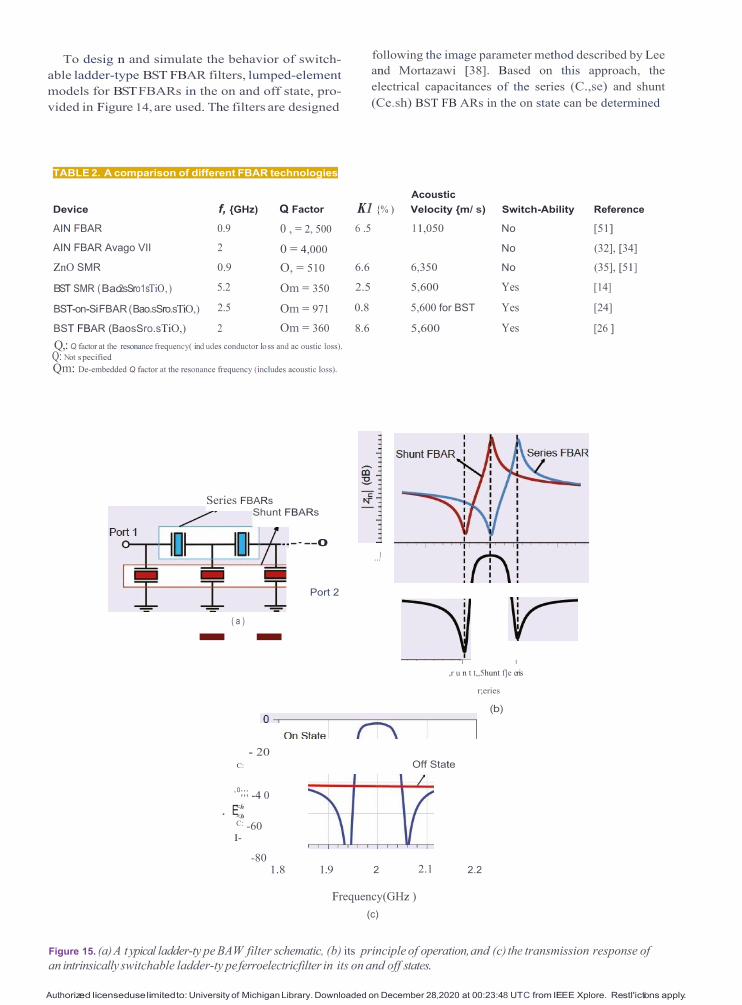
TABLE 2. A comparison of different FBAR technologies.
Device
f, {GHz)
Q Factor K1 {% )
Acoustic
Velocity {m/ s)
Switch-Ability
Reference
AIN FBAR 0.9 0 , = 2, 500 6 .5 11,050 No [51]
AIN FBAR Avago VII 2 0 = 4,000 No (32], [34]
ZnO SMR 0.9 O, = 510 6.6 6,350 No (35], [51]
BST SMR ( Bao.2sSro1sTiO, ) 5.2 Om = 350 2.5 5,600 Yes [14]
BST-on -Si FBAR ( Bao.sSro.sTiO ,) 2.5 Om = 971 0.8 5,600 for BST Yes [24]
BST FBAR (BaosSro.sTiO,) 2 Om = 360 8.6 5,600 Yes [26 ]
Q,: Q factor at the resonance frequency( ind udes conductor lo ss and ac oustic loss).
Q: Not specified.
Qm: De-embedded Q factor at the resonance frequency (includes acoustic loss).
Series FBARs Shunt FBARs
- - Port 2
( a )
I
,r u n t t,,5hunt f]e eris
r;eries
(b)
- 20 C:
Off State
·0;;; -4 0
. E<h
<h C: -60 I-
-80 1.8 1.9
2 2.1 2.2
Frequency(GHz )
(c)
Figure 15. (a) A t ypical ladder-ty pe BAW filter schematic, (b) its principle of operation, and (c) the transmission response of
an intrinsically switchable ladder-ty pe ferroelectricfilter in its on and off states.
..!

Authorized licenseduse limitedto: University of Michigan Library. Downloaded on December 28,2020 at 00:23:48 UTC from IEEE Xplore. Restl'ictoi ns apply.
May 2020 IEEE maowave magazine 129

Authorized licenseduse limitedto: Universityof Michigan Library. Downloaded on December 28,2020 at 00:23:48 UTC from IEEE Xplore. Restlictions apply.
Acoustically coupled filters can provide high out-of-band rejection while also maintaining a small footprint.
using (4) and (5), given the filter specification, includ
ing fractional BW (FBW), system impedance {Zo), and
filter center frequency (me). Next, the structure of the
BST resonators can be designed based on the 1D trans
mission line model discussed in Sis [17] to meet the
required filter constraints:
C , ,,. -- ( 1 !."")A .·.,✓. (M - l J (1 + v1 +-FBW2) - 2, mcZov M FBW2M
(4)
l /M ) x / (M - / f ( l + /l + FB W2) - 2, 2mcZo M FBW M
(5)
whereM is
A schematic of a 1.5-stage n-network ladder-type intrin
sically switchable BAW filter unit cell based on BST
FBARs and a photograph of a fabricated filter are shown
in Figure 16(a) and (b), respectively (39].
In thisfilter, the series FBAR is replaced by two dou
bled-sized FBARs to simplify the de biasing network,
while Rbtas models the high-resistivity biasing line for
the resonators. DC bias voltages are applied through
bias tees connected to each port of the device. The
measured transmission and reflection responses in the
filter's on and off states are provided in Figure 16(c) and
(d). In the on state, the filter provides a mini mum
insertion loss (IL) and FBW of 2.25 dB and 2.8%
{58 MHz at 2.08 GHz), respectively. Off-state isolation
between the input and output ports exceeds 14 dB. The
size of the filter active area occupies only 80 x 110 µm,
which is notably smaller than conventional piezoelec
tric filters.
Several filter unit cells can be cascaded in series to
design higher-order filters with higher out-of-band
rejection and isolation levels at the cost of a larger IL.
For example, a 2.5-stage ladder-type BST FBAR filter is
4
M= (1+/ 1- l;f r (6)
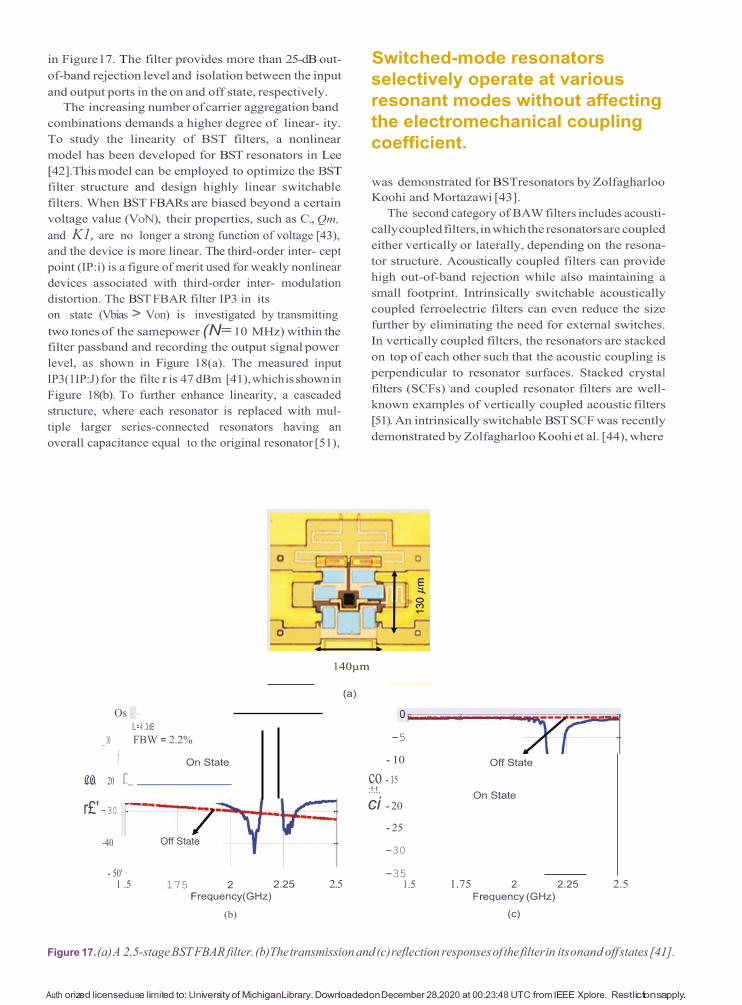
implemented in Zolfagharloo Koohi et al. [41]. A pho
tograph of the filter as well as the transmission and
reflection responses in its on and off states is shown
(a)
o ------------- - 5 On State
:c:!:o!.. - 10
·§;;;
- 15
- - 20 <I>
� - 25 i=
r o - 5
ai - 10 ::!:!.. c: - 1 5
0
- 20
- 25
(b)
= = = -- :::::===
On State Off State
-30
-35 -t--.---,--,-,----,---.,---,--,----,---t
-30
_35-+- - --- --,--. -
,----,--- ., ------ l
1.5 1.7 1.9 2.1 2.3 2.5
Frequency (GHz)
(c)
1.5 1.7 1.9 2.1 2.3 2.5
Frequency (GHz)
(d)
c,sh =(
&
,

Authorized licenseduse limitedto: Universityof Michigan Library. Downloaded on December 28,2020 at 00:23:48 UTC from IEEE Xplore. Restlictions apply.
Figure 16. (a) A 1.5-stage ladder-type BST FBAR filter unit cell and (b) the fabricated filter. The (c) measured transmission
and (d) reflection responses of the filter in its onand off states. (Adapted from [39].)
130 IEEE mcrONaVe magazine May 2020
Auth orized licenseduse limited to: University of MichiganLibrary. Downloadedon December 28,2020 at 00:23:48 UTC from IEEE Xplore. Restlictoi nsapply.
in Figure 17. The filter provides more than 25-dB out
of-band rejection level and isolation between the input
and output ports in the on and off state, respectively.
The increasing number of carrier aggregation band
combinations demands a higher degree of linear ity.
To study the linearity of BST filters, a nonlinear
model has been developed for BST resonators in Lee
[42].This model can be employed to optimize the BST
filter structure and design highly linear switchable
filters. When BST FBARs are biased beyond a certain
voltage value (VoN), their properties, such as C,, Qm,
and K1, are no longer a strong function of voltage [43),
and the device is more linear. The third-order inter cept
point (IP:i) is a figure of merit used for weakly nonlinear
devices associated with third-order inter modulation
distortion. The BST FBAR filter IP3 in its
on state (Vbias > Von) is investigated by transmitting
two tones of the samepower (N= 10 MHz) within the
filter passband and recording the output signal power
level, as shown in Figure 18(a). The measured input
IP3(1IP:J) for the filte r is 47 dBm [41), which is shown in
Figure 18(b). To further enhance linearity, a cascaded
structure, where each resonator is replaced with mul
tiple larger series-connected resonators having an
overall capacitance equal to the original resonator [51),
Switched-mode resonators
selectively operate at various
resonant modes without affecting
the electromechanical coupling
coefficient.
was demonstrated for BSTresonators by Zolfagharloo
Koohi and Mortazawi [43].
The second category of BAW filters includes acousti
cally coupled filters, in which the resonators are coupled
either vertically or laterally, depending on the resona
tor structure. Acoustically coupled filters can provide
high out-of-band rejection while also maintaining a
small footprint. Intrinsically switchable acoustically
coupled ferroelectric filters can even reduce the size
further by eliminating the need for external switches.
In vertically coupled filters, the resonators are stacked
on top of each other such that the acoustic coupling is
perpendicular to resonator surfaces. Stacked crystal
filters (SCFs) and coupled resonator filters are well
known examples of vertically coupled acoustic filters
[51). An intrinsically switchable BST SCF was recently
demonstrated by Zolfagharloo Koohi et al. [44), where
140µm
(a)
_ 10
:c!:o!-, 20
r£' - 3
-40
- 50' ·
1 .5
175 2 Frequency(GHz)
(b)
2.25 2.5
-5
- 10
co - 15 :!:!,
ci - 20
- 25
-30
-35 1.5
1.75
Off State
On State
2
Frequency (GHz)
(c)
2.25 2.5
Figure 17. (a) A 2.5-stage BST FBAR filter. (b)The transmission and (c) reflection responses of the filter in its onand off states [41].
Os - -
FBW = 2.2%
Off State

Auth orized licenseduse limited to: University of MichiganLibrary. Downloadedon December 28,2020 at 00:23:48 UTC from IEEE Xplore. Restlictoi nsapply.
May 2020 IEEEmaowave magazine 13 1

Authorized licenseduse limitedto: University of Michigan Library. Downloaded on December 28,2020 at 00:23:48 UTC from IEEE Xplore. Restlictions apply.
Spectrum Analyzer
Bias-Tee
OUT
the size of the filter unit cell was only 19 x 19 µm. In
laterally coupled acoustic filters, the resonators are fab
ricated on the same plane, separated by a gap between
the electrodes. In such filters, the acoustic coupling
takes place in a lateral direction parallel to the reso
nator surfaces. Monolithic CFs (MCFs), among the first
BAW filters to employ lateral coupling, have been used
since the 1960s for various applications, such as inter
mediate frequency filters in radios. Quartz crystals
havebeen the material of choice in trad itional MCFs.
Signal Generator
Power Supply
(a)
50
e
Recently, laterally coupled acoustic filters have been
implemented using thin-film piezoelectric materials
(AlN and ZnO). Due to their significantly diminished
thicknesses, thin-film laterally coupled acoustic fil
ters operate at much higher frequencies compared to
MCFs, making them suitable for RF and microwave
applications. An intrinsically switchable BTO-based
laterally coupled filter was designed and fabricated, as
shown in Figure19(a) [37]. The measured S-parameters
of the filter are provided in Figure 19(b) and (c). As
shown in the figure, the filter
can provide more than 40-dB
out-of-band rejection in the
on state and isolation between
the input and the output ports
in the off state.
Intrinsically Switchable Filter Banks In trinsica lly switchable BST
filters of different frequencies
are connected in parallel to
form intrinsically switchable
multiband filter banks. The
ID
<ii
a.. :, :,
Q.
0
0
- 50
- 100
0 10 20 30 40 50
Available Input Power (dBm)
(b)
ultimate goal of ferroelectric
filter banks is to eliminate the
switches dedicated to selecting
the frequency bands from the
RF module. A possible way of
realizing intrinsically switch
able ferroelectric filter banks is
experimentally demonstrated
by Zolfagharloo Koohi and
Mortazawi [45], [46]. A triple
band intrinsically switchable
Figure 18. (a) A two-tone measurement setup for intermodulation distortion of the
2.5-stage BST FBAR filter and (b) its measured IP3 data [41]. DUT: device under test;
GSG: ground- signal- ground.
filter bank is designed and
fabricated, where each filter
ing path consists of a 2.5-stage
0 0 Off
- 10 - 5
co - 20 co
J - 30
-40 i
- 50 0.5 0.6
:!:!, - 10
CJ)
- 15
- 20
0.7 0.8 0.9 1.1 0.5
0.6 0.7
0.8 0.9 1.1
Frequency(GHz) Frequency (GHz)
(a) (b) (c)
Figure 19. (a) A fabricated intrinsically switchable acoustically coupled BTO filter. The (b) transmission and (c) reflection
response of the filter in its onand off states. (Adapted from [37].)
,,,
? /
,,,,,,
II
-- Fundamental
--- IM3
Cl Measurement
Spurious Resonance
35dB
O n
I

Authorized licenseduse limitedto: University of Michigan Library. Downloaded on December 28,2020 at 00:23:48 UTC from IEEE Xplore. Restlictions apply.
132 IEEEmcrONaVe magazine May 2020

Authorized licensed use limited to: University of Michigan Library. Downloadedon December 28,2020 at 00:23:48 UTC from IEEE Xplore. Restlictoi nsapply.
- ra •
.
□
ladder-type BST filter placed between seriesBST metal
insulator- metal varactors, as shown in Figure 20. The
purpose of using BST varactors here is to improve the
isolation of the filter without significantly impacting IL
or adding to fabrication complexity.
The intrinsically switchable filter bank operates as
follows. When a filter path is switched on, its constitu
ent resonators are turned on, and the varactors are
tuned to their highest capacitance such that they are at
their lowest impedance, which occurs when the volt
age across their terminals is set to 0 V. When the filter
is switched off, the constituting resonators are turned
off, and the varactors are set to their lowest capacitance
such that they present a high impedance, which occurs
when the voltage across their terminals is high.
In thisexample, the BST varactors are fabricated on
the same Si wafer along with the BST FBARs using a
similar fabrication process; therefore, the filter bank
structure and the fabrication process are simplified,
and the overall footprint of the filter bank is reduced,
compared to traditional piezoelectric filter banks
where external switches are employed. The series
varactors in Figure 20 are either under zero bias or
large bias voltage and are not used in their voltage
sensitive region. Therefore, the addition of BST varac
provides bandpass responses with center frequencies
of 1.85,1.96, and 2.04 GHz, respectively. The size of the
active area for this filter bank is only 250 X 480 µm,
which is significantly reduced compared to previously
reported switchable acoustic filter banks based on
piezoelectric materials [46]. The larger IL of the mea
sured filter bank, compared to the standalone filter of
Figure 17, is mostly attributed to the varactors' losses,
due to the fact that the BST depos ition conditions in
this article are not optimized for varactor fabrication.
The intrinsically switchable ferroe lectric filter bank
example presented here demonstrates the feasibility of
fabricating BST-based switchable filter banks. How
ever, optimized BST filter banks are yet to be designed
to meet state-of-the-art RF front-end specifications.
Future work involves the enhancement of BST FBARs'
figureof merit (Qm X K ) as well as the development of
a design methodology for the switchable filter banks.
Improving BST FBARs' parameters (Qm and K?) is
essential for designing low-loss switchable filters and
is part of the ongoing research efforts following the
methods described previously. The simulation results
<-----------
tors to the filter structure in this example does not ---------- • Bias --.:::::::_-_., Lines
contribute significantly to the nonlinearity of the filter.
To further reduce the effect of varactors on linearity,
BST varactor linearization techniques presented by Fu
et al. [47] can also be employed. The basic concept
described in Fu et al. [47] is to reduce the RF swing
across the ferroelectr ic varactors by connecting mul
tiple capacitors in series.
A photog raph of the fabricated triple-band BST
FBAR filter is shown in Figure 21(a), and its measure
I - CJ w□
LJ i _r - c· _J •
- t:i .. ... .
c:i
i:l ( >--- Bias { ,
ment results are depicted in Figure 21(b.) In this case,
with all filters switched off, the signal transmission
is lower than - 27dBover the frequency range of 1.5-
2.5 GHz (off-state transmission is shown by a dashed
line). Turning on each of the three individual filters
0
- 10
cc
't l ines ' i'
(a)
de Bias Control
Figure 20. Thedesigned multiband 2.5-stage BST FBAR
filter. The bias network is represented bydashed lines.

Authorized licensed use limited to: University of Michigan Library. Downloadedon December 28,2020 at 00:23:48 UTC from IEEE Xplore. Restlictoi nsapply.
re - 20
- 30
-40
1.5 1.75 2 2.25 2.5 Frequency (GHz)
(b)
Figure 21. (a) The fabricated triple -bandBST FBAR filter
and (b) its measured transmission response. Tlie measured
off-state(whenall of the filters are turned off) response is
also provided in adashed line. (Adapted from [46 ]. )
May 2020 IEEE maowave magazine 133

Authorized licenseduse limitedto: University of MichiganLibrary.Downloadedon December28,2020 at 00:23:48 UTC from IEEE Xplore. Restl'ictoi ns apply.
0
- 10
co -20
- 30
ci' --40
-50
---60
1.5 1 .6 1. 7 1.8 1 .9 2
Frequency (GHz)
2.1 2.2
Future work includes further optimization of thin-film
BST composition and deposition conditions for design
ing resonators with an improved Qm and Kr. F ur ther
more, a systematic design process must bedeveloped for
low-loss, multiban d filters and filter banks.
References [1] "Ericsson mobility report," Ericsson, Stockholm, Sweden, Nov.
2018, [Online]. Available: https :/ / www.ericsson.com/assets/ local/
mobility-report/documents/201/8ericsson-mobiltiy-report-november
-2018.pdf
[2] R.Ru,by "A snapshot in time: The futurein filters for cell phones,"
IEEE Mierow.Mag., vol.16, no. 7, pp. 46-59, Aug. 2015. doi: 10.1109/
MMM.2015.2429513.
[3] A. Hagelauer, G. Fattinger, C. C. W. Ruppel,M. Ueda, K. Hashimo
Figure 22. The simulation results for a switchable filter
bank consisting of four 2.5-stagefilters in their on state,
superimposed in one figure.
of a switchable filter bank using a circuit topology
similar to Figure 20 based on BST FBARs with a Kr and Qm of 8% and 800, respectively, are shown in Fig
ure 22. In this simulation, a modest capacitance tun
ability of 4:1for BST varactors (Qvar = 100) and a shunt
inductance of 3.5 nH (Qind = 50) are assu med. Based
on these parameters, the intrinsically switchable fil
ter bank provides a minimum IL of 2 dB, out-of-band
rejection and isolation levels of more than 40 dB, and
an FBW of 3% at center frequencies of 1.7, 1.8, 1.9, and
2 GHz. The performance of the filterbank can be further
enhanced by optimizing the filter-bank configuration
for minimizing the reactive loading effect of the off
state filters without using varactors. A possible way is
to employ the approaches developed for the synthe
sis of multiplexerswith the manifold configuration as
described in Bonastre [48] and Fattinger et al. [49].
Summary and Conclusions
Sales of RF front ends are expected to reach US$18 bil
lionby 2020, and the growingnumberof required RFfil
ters is the main driver for this businessopportunity [50].
For multiband operation, RF filters are currently used
in conjunction with switchplexers to select the desired
bands and mode of operation. The switches within RF
modules can be eliminated by employing reconfigu
rable filters to considerably reduce the size, complexity,
and cost of future RFfront ends. This article reviewed
recent progress on reconfigurable RF acoustic devices
based on thin-film ferroelectric BST. Ferroelectric BST
possesses several unique characteristics, including
electric-field-induced piezoelectricity, field-dependent
permittivity, and high relative permittivity, that are
employed in the design of reconfigurable RF devices.
The BST devices discussed here demonstrate the feasi
bility of fabricating intrinsically switchable resonators,
filters, and filter banks aimed at simplifying future RF
frontendsbyeliminating the need for external switches.
t,o and A. Tag,"Microwave acoustic wave devices: recent advances
on architectures,modeling, materia,ls and packaging," IEEE Trans.
Mierow. Theory Techt1., vo l. 66, no. 10, pp. 4548-4562, Oct. 2018. doi:
10.110/91MTI.2018.2856401.
[4] I. J. Busch Vishniac, "Trends in electromechanical transduction,"
Phys. Today, vol. 51,no. 7, pp. ,28 1998. doi: 10.1063/ 1.88232.5
[5]F.D. Bannon, J. R.Clark, and C. T.C. Nguyen, "High-Q HF micro
electromechanical filters," IEEE J. Solid-StateCircui.t s, vol.,35 no. 4, pp.
512-526, 2000. doi: 10.1109/4.839911.
[6] S. Pourkamali, A. Hashimura, R. Abdolvand, G. K. Ho, A. Erbil,
and F. Ayazi, "H igh-Q single crystal silicon HARPSS capacitive
beam resonators with self-alignedsub-100-nmtransduction gaps,"
J. Mieroeleclromec,l. Syst., vol. 12, no. 4, pp. 487-4%, Aug. 2003. doi:
10.1109/ JMEMS.2003.811726.
[7] J. Wang, Z. Ren, and C. T. Nguyen, "1.156-GHz self-aligned vibrat
ing micromechankal disk resonator", IEEE Trat1s. Ultraso, n. Fer
roelect., Freq. Control, vol.51, no. 12, pp. 1607-1628, Dec. 2004. doi:
10.1109/ TUFFC.2004.1386769.
[8] A. Ozgurluk, M. Akgul, and C. T. Nguyen, "RFchannel-select mi
cromechanical disk filters-Part I:Design," IEEE Trans . Ultrason .,
Ferroele,ct. Freq. Control, vol. 66, no. 1, pp. 192-217, Jan. 2019. doi:
10.1109/ TUFFC.2018.2881727.
[9] X. Zhu,J. D. Phillips,and A. Mortazawi, "A DC voltagedependant
switchable thin film bulk wave acoustic resonator using ferroelec tric
thin film," in Proc. IEEE MTT -S Int. Microwave Symp . Dig., June 2007,
pp . 671- 674. doi:10.1109/ MWSYM.2007.380009.
[10] J. Berge, A. Vorobiev, W. Steichen , and S. Gevorgia n, "Tun able
solidly mounted thin film bulk acoustic resonators based on
Ba,Sr1_,TiO 3 films," IEEE Mierow. Compon. Lett., vol.,17 no. 9, pp.
655- 657,Sept . 2007. doi:10.1109/ LMWC.2007.903445.
[11] A. Noet,h T. Yamada, A. K. Tagantsev , and N. Setter, "Electrical
tun ing of de bias induced acoustic resonances in paraelectric thin
films", J. A ppl. Phys.,vol.104, no. 9, Nov. 2008, Art. no. 094102. doi:
10.106/31.299964.2
[12] X. Zhu, V. Lee, J. Phillips, and A. Mortazawi, "An intrinsically
switchable FBAR filte r based on barium titanate thin films," IEEE
Mierow. Con1pot1. Lett., vo l. 19, no. 6, pp. 359-361, June 2009. doi:
10.1109/ LMWC.2009.2020013.
[13] A. Vorobiev, S. Gevorgian , M. Loffler, and E. Olsson, "Correla
tions between microstructure and Q-factor of tunable thin film bulk
acoustic wave resonators," /. Appl. Pliys., vol. 110, no. 5, 2011, Art. no.
054102. doi:10.106/31.3626939.
[14] A. Vorobiev, J. Berg,e S. Gevorgia n, M. Loff,ler and E. Olsson, "Ef
fect of interface roughness on acoustic loss in tunable thin film bulk
acoustic wave resonators," J. Appl. Phys., vol. 110, no. 2, 2011, Art.
no.024116. do i: 10.1063/ 1.3610513.
[15] S. Lee, V. Lee, S. A. Sis, and A. Mortazawi, "Large-signal per
formance and modeling of intrinsically switchable ferroelectric
FBARs", IEEE Trans. Mierow. Theory Tee/in ., vol. 61, no. 1, pp. 415-
422,Jan. 2013. doi:10.1109/ TMTT.201.22225442.
[16]S. A. Sis, S. Lee, V. Lee, A. Bayraktaroglu, J. Philips , and A. Mor
tazawi, "Intrinsically switchable, high-Q ferroelectric-on-silicon
composite film bulk acoustic resonators," IEEE Trans. Ultrason.,
134 IEEE mcrONaVe magazine May 2020
r',, ...... ( "'I /
'
- - -
'J " / -<i / t,(3 II"" ..,... r
Authorized licenseduse limitedto: University of MichiganLibrary.Downloadedon December28,2020 at 00:23:48 UTC from IEEE Xplore. Restl'ictoi ns apply.
m .
Ferroelect., Freq. Control, vol.,61 no. 2, pp. 231- 238,Feb. 2014. doi:
10.1109/TUFFC.2014.6722609.
[17]S. A. Sis,"Ferroelectric-on-siliconswitchable bulk acoustic wave
resonators and filters for RFapplications," Ph.D.dissertation, Univ.
Michigan, Ann Arbor, 2014.
[18] R. York, "Tunable dielectrics for RF circuits," in Multifunctianal
Adaptive Microwave Circuits and Systems, M.Steer and W.D. Palmer
Eds., Raleigh, NC: Scitech, 2009.
(19] S. Gevorgian, Ferroelectrics in Micruwaoe Devices, Circ11its and Sys
tems:Pl,ysics, Modeling, Fabrication and Meas11rements (EngineeringMa
terials and Processes). London:Springer-Verlag,2009.
(20] S. Gevo rgian , A. Tagantsev, and A. K. Vorobiev, Tuneable Film 811/k
Acoustic Waoe Resonators (Engineering Materials and Processes).
London: Springer-Verlag,2013.
(21] A. Tombak, J.-P. Maria, F. T. Ayguavives, Z. Jin, G. T. Stauf, A. L
Kinge n, and A. Mortazawi, "Tunable barium strontium Hta nate
thin film capacitors for RF and microwave applications," IEEE
Mierow. Comp. Lett.,vol.12, pp. 3-5,Jan. 2002. doi: 10.110/97260.
97571.6
(22] N. K. Pervez, P. J. Hansen, and R. A. York, "High tunability
barium strontium titanate thin films for RF circuit applications,"
Appl. Phys. Lett., vol. 85, no. 19, pp. 4451-4453, Nov. 2004. doi:
(35) K.Kokkonen and T.Pensala,"4E-4 laser interferometr ic measure
ments and simulations of waves transm itted through the acoustic
mirror in thin film BAW resonator," in Proc. 2006 IEEE Ultrasonics
Symp., Vancouver, BC, pp. 460-463. doi: 10.1109/ULTSYM.2006.123.
(36]G. N. Sadd ik and R.A. York,"An L-section de electric field switch
able bulk acoustic wave solidly mounted resonator filter based on
Baos S_r 0 5 TiOs," IEEE Trans. Ultrason., Ferroelect., Freq. Contro l, vol.
59,no. 9, pp. 2036- 2041,Sept. 2012. doi:10.1109/ lSAF.2011.6014000.
(37) S. A. Sis, S. Lee, V. Lee, and A. Mortazawi, "An intr insically
switchable, monolithic BAW fil ter using ferroelectric BST," IEEE
Mierow.Compon. Lett., vol.26, no. 1, pp. 25-27,Jan.2016.doi:10.1109/
LMWC.2015.2505623.
(38] S. Lee and A. Mortazawi, "BAW filter design method based on in
trinsically switchableferroelectric BSTFBARs," in Proc. IEEE MIT Int.
Mierow. Symp.(IMS),May2016.d oi: 101. 109/MWSYM.20167.540105.
(39] M . Zolfagharloo Koohi, S. Lee, and A. Mortazawi, "Fabrication
of a Low insertio n Joss intrinsically switchable BAW filter based
on BST FBARs," in Proc. 2017 IEEE MTT Int. Mierow. Symp.(IMS),
Honololu, HI, pp. 1480-1483. doi:10. 09/ MWSYM.2017.805890. 0
(40] M. Zolfagha rloo Koohi, S. Nam, and A. Mortaza,wi "Intrinsically
switchable and bandwidth reconfigurable FBAR filter employing
electrostriction in ferroelectric BST,"in Proc. IEEE MIT Int.Mierow.
10.1063/1.1818724. Symp.(IMS ),June 2018. doi:10.1109M/ WSYM.2018.8439509.
(23] D.-Y.Chen and J. D. Phillips, "Electric field dependence of piezo
electric coefficient in ferroelect ric thin films," /. Electroceram., vol.
17, nos.2-,4 pp.613-617, 2006. doi:10.1007/s10832-006-9335-0.
(24)S. Lee and A. Mortazawi, "An intrinsicallyswitchable ladder-type
ferroelectric BST-on-Si composite FBAR filter," IEEE Trans . Ultra
so, n. Ferroelect., Freq. Control, vol. 63, no. 3, pp. 456-462, Mar. 2016.
doi:10. 09/ TUFFC.2016.2516743.
(25] S. Lee, M. Zolfagharloo Koohi, and A. Mortazawi, "Lateral-wave
spurious-modeselimination in switchable ferroelectric BST-on-Si
composite FBARs," in Proc. IEEE MIT Int. Mierow. Symp. (IMS),
May 2016, pp. 1-4.doi:10.109/ MWSYM.2016.7450120.
(26] M. Zolfagharloo Koohi, S. Lee, and A. Mortazawi, "High QmxJ<2.
intr insically sw itchable bst thi n film bulk acoustic resonators," in
Proc.IEEE MIT Int.Mierow.Symp.(IMS ), June2017,pp. 296-299.doi:
10.1109/MWSYM.2017.8059101.
(27] V. Lee, "Switchablea nd tunable ferroelectric devices for adaptive
and reconfigurable RF circuits," Ph.D. dissertation, Univ. Michi
gan,Ann Arbor, 2014.
(28] V. Lee, S. A. Sis, J. D. Phillips, and A. Mortazawi, "Intrinsically
switchable ferroelectric contour mode resonators," IEEE Trans.
Mierow. Theory Techn., vol. 61, no. 8, pp. 2806-2813, Aug. 2013. doi:
10.1109/TMTT.201.32271756.
(29] S. Gevorgian and A. Vorobiev, "Impedance of DC-bias-con
trolled composite FBARs," IEEE Trans. Ultrason., Ferroele,ct. Freq.
Control, vol. 60, no. 4, pp. 795-804, Apr. 2013. doi: 10.1109/
TUFFC.2013.2628.
(30] S. V. Ptashn ik e t a l., "Ferroe lectric thin film acousticdevices with
electrical multiband switching ability," Sci. Rep., vol. 7, no. 1, 2017,
Art. no.15289. doi : 10.1038/s41598-017-14895-8.
(31] M. Zolfagharloo Koohi and A. Mortazawi, "Switched mode thin
film bulk acoustic wave resonators," in Proc. 2019 IEEE MIT Int.
Mierow. Symp. (IMS ), pp. 528- 531. doi: 10.1109/MWSYM.2019.
8700959.
(32) C. C. W. Ruppel, "Acoustic wave filter technology- A review,"
IEEE Trans. Ultrason., Ferroelect., Freq. Control, vol. 64, no. 9, pp.
1390-1400, Sept.2017. do i: 10.1109/TUFFC.2017.2690905.
(33) M. Zolfaghar loo Koohi and A. Mortazawi, "Negative piezoelec
tric based electric-field-actuated mode-switchable multilayer BST
FBARs for selectivecontrol of harmonic resonances without degrad
ing K.i" IEEE Trans.Ultrasonics, Ferroelectrics, and Frequency Cuntrol,
to be published.
(34] R. Ruby, "A decade of FBAR success and what is needed for an
other successful decade," Proc. 2011 Symp. Piezoelectricity, Acoust·ic
Waves and Device Applications (SPAWDA), Shenzhen, pp. 365-369.
doi:10. 109/SPAWDA.20111.67265.
(41] M. Zolfagharloo Koohi, S. Lee, and A. Mortazawi, "Compact in
trinsically switchable FBAR filters utilizing ferroelectric BST,"
IEEE Trans. Ultrason., Fe-rroel ect., Freq . Control, vol. 65, no. 8, pp.
1468-1474,Aug. 2018. doi:10.1109/TUFFC.2018.2839756.
(42] S. Lee, "Design and modeling of ferroelectric BST FBARs for
switchable RF bulk acoustic wave filters,"Ph.D. dissertation, Univ.
Michigan, Ann Arbor, 2016.
(43] M . Zolfagharloo Koohi and A. Mortazawi, "On the linearity of
BST thi n film bulk acoustic resonators," in Proc. 2018 IEEE MIT -S
Int. Microwaoe Workshop Series on Advanced Materials and Processes
RF and THz Applications (IMWS -AM P), Ann Arbor, Ml, 2018, pp. 1-
3. doi:10. 109/lMWS-AMP.2018.8457167.
(44] M. Zolfagharloo Koohi, S. Nam, A. Mortazawi "Intrinsically
switchable miniature ferroelectric stacked crystal filters," in Proc.
2019 IEEE MIT Int. Mierow. Symp. (IMS), pp. 661-664. doi: 10.1109/
MWSYM.2019.8700965.
(45] M. Zolfagharloo Koohi and A. Mortazawi, "A compact intrinsi
cally switchable filter bank employing multifunctional ferroelec tric
BST,"in Proc. IEEE MIT Int. Mierow. Symp. (IMS),June 2018, pp.
849-851. doi:10. 109/MWSYM.2018.8439700.
(46] M. Zolfagharloo Koohi and A. Mortazawi, "Intrinsically switch
ablefilter bankemployingferroelectric barium strontium titanate,"
IEEE Trans . Mierow.Theory Techn.,vol.66,no.12,pp. 5501-5507, Dec.
2018. doi:10.1109/TMTT.2018.2867196.
(47] J. Fu, X. A. Zhu, J. D. Phillips, and A. Mortazawi, "Improving
linearity of ferroelectric-based microwave tuna ble circuits," IEEE
Trans. Mierow. Theory Teclm., vol. 55, no. 2, pp. 354-360, Feb. 2007.
doi:10. 109/ TMTT.2006.88932. 3
(48] A. R. G. Bonastre, "RF filters and multiplexers based on acous
tic wave technologies with ladder-type and cross-coupledtopolo
gies," Ph.D. dissertation, Universitat Autonoma de Barcelona, Bel
laterra, Spain,2016.
(49] G. G. Fattinger et al.,"Carrier aggregation and its challenges - or: The
golden age for acoustic filters," Proc. 2016 IEEE MIT-S Int. Microwaue
Symp.(IMS),SanFrancis,co pp.1-4.doi:10.1109/ MWSYM.2016.7540211.
(50) "Qualcomm and TDK form joint venture to provide industry
leading RF front-end solutions for mobile devices," Qualcom,m
San Diego, CA, Jan. 12, 2016, (Online]. Available: https:// www
.qualcomm.com/ news/ releases/ 2016/ 01/12/ qualcomm-and -tdk
-form-joint-vent ure-provide-ind ustry-leading-rf-front -end
(51] K. Hashimoto, RF Bu/Jc Acoustic Wave Filters for Communicati,ons
Norwood, MA: Artech House, 2009.
(52] S. Gevorgian,"Agile microwavedevices," IEEE Micraw. Mag.,vol.,10
no. 5, pp. 93-98, Aug.2009.d oi: 10.1109/MMM.2009.932830.

Authorized licenseduse limitedto: University of MichiganLibrary.Downloadedon December28,2020 at 00:23:48 UTC from IEEE Xplore. Restl'ictoi ns apply.
May 2020 IEEE maowave magazine 135
Related Documents