Recent progress in understanding of lattice defects in Czochralski- grown germanium: catching-up with silicon J. Vanhellemont 1,a , S. Hens 1 , J. Lauwaert 1 , O. De Gryse 1 , P. Vanmeerbeek 1 , D. Poelman 1 , P. Śpiewak 2 , I. Romandic 3 , A. Theuwis 3 and P. Clauws 1 1 Dep. of Solid State Sciences, Ghent University, Krijgslaan 281 S1, B-9000 Ghent, Belgium 2 Materials Design Division, Faculty of Materials Science and Engineering, Warsaw University of Technology, Wołoska 141, 02-507 Warsaw, Poland 3 Umicore EOM, Watertorenstraat 33, B-2250 Olen, Belgium a [email protected] Keywords: germanium, silicon, vacancies, voids, simulation, oxygen, precipitation, FTIR Abstract. Recent progress is presented in the understanding of grown-in defects in Czochralski- grown germanium crystals with special emphasis on intrinsic point defects, on vacancy clustering and on interstitial oxygen. Whenever useful the results are compared with those obtained for silicon. Introduction Today the main application of polished germanium wafers is as heavily doped substrate for GaAs epitaxy in order to produce high efficiency solar cells for space applications. Due to its higher intrinsic carrier mobility compared to silicon, however, the use of moderately doped germanium based substrates is being reconsidered for application in advanced nano-electronic devices. 200 and 300 mm germanium (001) oriented dislocation free substrates have recently become available and germanium on insulator (GeOI) substrates are being developed [1]. For a successful application as substrate material, these novel germanium based substrates will have to meet the stringent requirements defined in the SIA road map. One of these requirements is the absence of extended lattice defects of which the formation depends strongly on the presence and properties of point defects either introduced during crystal pulling or during wafer processing. In contrast to silicon, the properties of the intrinsic and extrinsic point defects in germanium are not well-known and a significant research effort with that respect will be needed in the coming years [2]. Intrinsic point defects in germanium Mainly three approaches have been used to directly study intrinsic point defect properties in germanium [3]: quenching from high temperatures followed by annealing at lower temperatures, plastic deformation at high temperatures and irradiation at low temperatures in order to create Frenkel pairs and individual point defects. In addition, the study of the diffusion and/or precipitation of fast diffusing dopants such as Cu and Zn can provide indirect information on intrinsic point defects. Finally, also ab initio calculations can shed more light on the formation and migration energy and the electrical activity of the intrinsic point defects. The quenching technique has been very successful in the assessment of vacancy properties in metals and has therefore initially also been used extensively for germanium. These preliminary results demonstrated that quenching of n-type Ge above 800 o C resulted in p-type material, pointing to the creation of quenched-in acceptors. Annealing at 500 o C recovered the original n-type, indicating the out-diffusion/annihilation of the quenched-in thermal acceptors. It was soon realized however that the early experiments suffered from copper contamination, whereby substitutional copper is a triple Solid State Phenomena Vols. 108-109 (2005) pp 683-690 Online available since 2005/Dec/15 at www.scientific.net © (2005) Trans Tech Publications, Switzerland doi:10.4028/www.scientific.net/SSP.108-109.683 All rights reserved. No part of contents of this paper may be reproduced or transmitted in any form or by any means without the written permission of TTP, www.ttp.net. (ID: 157.193.1.245, Ghent University, Belgium-09/07/13,13:11:43)

Welcome message from author
This document is posted to help you gain knowledge. Please leave a comment to let me know what you think about it! Share it to your friends and learn new things together.
Transcript

Recent progress in understanding of lattice defects in Czochralski-
grown germanium: catching-up with silicon
J. Vanhellemont1,a, S. Hens1, J. Lauwaert1, O. De Gryse1, P. Vanmeerbeek1, D. Poelman1, P. Śpiewak2, I. Romandic3 , A. Theuwis3 and P. Clauws1
1Dep. of Solid State Sciences, Ghent University, Krijgslaan 281 S1, B-9000 Ghent, Belgium 2Materials Design Division, Faculty of Materials Science and Engineering, Warsaw University of
Technology, Wołoska 141, 02-507 Warsaw, Poland 3Umicore EOM, Watertorenstraat 33, B-2250 Olen, Belgium
Keywords: germanium, silicon, vacancies, voids, simulation, oxygen, precipitation, FTIR
Abstract. Recent progress is presented in the understanding of grown-in defects in Czochralski-
grown germanium crystals with special emphasis on intrinsic point defects, on vacancy clustering
and on interstitial oxygen. Whenever useful the results are compared with those obtained for silicon.
Introduction
Today the main application of polished germanium wafers is as heavily doped substrate for GaAs
epitaxy in order to produce high efficiency solar cells for space applications. Due to its higher
intrinsic carrier mobility compared to silicon, however, the use of moderately doped germanium
based substrates is being reconsidered for application in advanced nano-electronic devices. 200 and
300 mm germanium (001) oriented dislocation free substrates have recently become available and
germanium on insulator (GeOI) substrates are being developed [1]. For a successful application as
substrate material, these novel germanium based substrates will have to meet the stringent
requirements defined in the SIA road map. One of these requirements is the absence of extended
lattice defects of which the formation depends strongly on the presence and properties of point
defects either introduced during crystal pulling or during wafer processing. In contrast to silicon,
the properties of the intrinsic and extrinsic point defects in germanium are not well-known and a
significant research effort with that respect will be needed in the coming years [2].
Intrinsic point defects in germanium
Mainly three approaches have been used to directly study intrinsic point defect properties in
germanium [3]: quenching from high temperatures followed by annealing at lower temperatures,
plastic deformation at high temperatures and irradiation at low temperatures in order to create
Frenkel pairs and individual point defects. In addition, the study of the diffusion and/or precipitation
of fast diffusing dopants such as Cu and Zn can provide indirect information on intrinsic point
defects. Finally, also ab initio calculations can shed more light on the formation and migration
energy and the electrical activity of the intrinsic point defects.
The quenching technique has been very successful in the assessment of vacancy properties in metals
and has therefore initially also been used extensively for germanium. These preliminary results
demonstrated that quenching of n-type Ge above 800oC resulted in p-type material, pointing to the
creation of quenched-in acceptors. Annealing at 500oC recovered the original n-type, indicating the
out-diffusion/annihilation of the quenched-in thermal acceptors. It was soon realized however that
the early experiments suffered from copper contamination, whereby substitutional copper is a triple
Solid State Phenomena Vols. 108-109 (2005) pp 683-690Online available since 2005/Dec/15 at www.scientific.net© (2005) Trans Tech Publications, Switzerlanddoi:10.4028/www.scientific.net/SSP.108-109.683
All rights reserved. No part of contents of this paper may be reproduced or transmitted in any form or by any means without the written permission of TTP,www.ttp.net. (ID: 157.193.1.245, Ghent University, Belgium-09/07/13,13:11:43)

acceptor. Further more it soon became clear that quenching experiments cannot yield information on
single vacancies as diffusion is so fast that vacancy clustering during quenching cannot be avoided.
Self-diffusion in Ge is the slowest diffusion process and provides direct evidence of the existence of
an equilibrium concentration of intrinsic point defects. Recent experiments of Giese et al [4]
showed that in contrast to silicon, the self-diffusion coefficient GeD in germanium
(=3.09
2 113.6eV
kTe cm s− − ) is dominated by vacancies. They indeed presented strong experimental
evidence that the vacancy assisted Ge tracer diffusion coefficient *
( ) 0.5V V V
Ge
Ge
C DD
C= is very close to
* *
0.5 0.73V V I I
Ge
Ge Ge
C D C DD
C C= + or * *
I I V VC D C D<< , (1)
which is the opposite of the behavior in silicon. IC
∗ and VC
∗ are the thermal equilibrium self-
interstitial and vacancy concentrations, respectively. CGe is the concentration of germanium lattice
atoms.
Thermal equilibrium concentration of vacancies. Little information can be found on the thermal
equilibrium vacancy concentration *
VC . On the basis of annealing experiments on thermal acceptors
quenched into germanium, Mayburg [5] obtained
2.01
* 23 33 10eV
kT
VC e cm
− −= × , (2)
predicting an equilibrium vacancy concentration of 1.3×1015cm−3 at melt temperature. This is in
good agreement with the estimate of 2.9 − 3.9 ×1015cm−3 that Tweet [6] obtained based on Cu
precipitation and diffusion behavior.
According to Giese et al [4] one can write
3.09
* 24 1 11.18 10eV
kT
V VC D e cm s
− − −= × . (3)
Combining Eq. 2 and Eq. 3 leads to
DV= 3.9e
−1.08eV
kT cm2s−1 . (4)
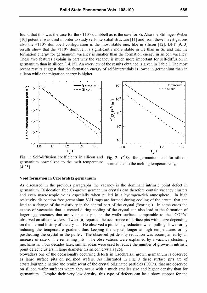
Fig. 2 shows *
V VC D for germanium and for silicon as a function of the normalized temperature.
Simulation of intrinsic point defect properties. As reliable experimental data for intrinsic point
defects in germanium are still lacking to a large extent, molecular dynamics calculations and
comparison with results obtained for silicon can yield useful information. Already in 1982,
Mashovets [7] published an extensive review on this topic of which the main results concerning
formation and migration energies of self-interstitials and vacancies are represented in Table I
together with more recent results.
Bernstein et al. [8] studied a number of properties of germanium using non-orthogonal tight-binding
(TB) calculations. In case of point defects, these calculations include the vacancy, as well as three
interstitial positions, the tetrahedral, hexagonal, and <110> dumbbell. TB indicated that the lowest-
energy interstitial was the tetrahedral configuration, in contrast with DFT [9] simulations which
684 Gettering and Defect Engineering in Semiconductor Technology XI
found that this was the case for the <110> dumbbell as is the case for Si. Also the Stillinger-Weber
[10] potential was used in order to study self-interstitial structure [11] and from these investigations
also the <110> dumbbell configuration is the most stable one, like in silicon [12]. DFT [9,13]
results show that the <110> dumbbell is significantly more stable in Ge than in Si, and that the
formation energy for germanium vacancy is smaller than the formation energy in silicon vacancy.
These two features explain in part why the vacancy is much more important for self-diffusion in
germanium than in silicon [14,15]. An overview of the results obtained is given in Table I. The most
recent results suggest that the formation energy of self-interstitials is lower in germanium than in
silicon while the migration energy is higher.
Fig. 1: Self-diffusion coefficients in silicon and
germanium normalized to the melt temperature
[4,25].
Fig. 2: *
V VC D for germanium and for silicon,
normalized to the melting temperature Tm.
Void formation in Czochralski germanium
As discussed in the previous paragraphs the vacancy is the dominant intrinsic point defect in
germanium. Dislocation free Cz-grown germanium crystals can therefore contain vacancy clusters
and even macroscopic voids especially when pulled in a hydrogen-rich atmosphere. In high
resistivity dislocation free germanium V2H traps are formed during cooling of the crystal that can
lead to a change of the resistivity in the central part of the crystal (“coring”). In some cases the
excess of vacancies that is created during cooling of the crystal can also lead to the formation of
larger agglomerates that are visible as pits on the wafer surface, comparable to the “COP’s”
observed on silicon wafers. Tweet [6] reported the occurrence of surface pits with a size depending
on the thermal history of the crystal. He observed a pit density reduction when pulling slower or by
reducing the temperature gradient thus keeping the crystal longer at high temperatures or by
postheating the crystal in the puller. The observed pit density reduction was accompanied by an
increase of size of the remaining pits. The observations were explained by a vacancy clustering
mechanism. Four decades later, similar ideas were used to reduce the number of grown-in intrinsic
point defect clusters in large diameter Cz silicon crystals [25].
Nowadays one of the occasionally occurring defects in Czochralski grown germanium is observed
as large surface pits on polished wafers. As illustrated in Fig. 3 these surface pits are of
crystallographic nature and reminiscent of the crystal originated particles (COP's) that are observed
on silicon wafer surfaces where they occur with a much smaller size and higher density than for
germanium. Despite their very low density, this type of defects can be a show stopper for the
Solid State Phenomena Vols. 108-109 685

production of GeOI wafers and for their use for IC processing. A thorough understanding of the
process parameters leading to pit formation is therefore essential.
Assuming that the observed pits are formed by vacancy clustering and vacancy diffusion limited
growth, on can make a crude estimate of the expected size (and density) as for silicon [26,27]
writing for the edge size of an octahedral void
( )0.5Vl D tλ= with ( )
0.50 *1
3
,
8 V V
Si Ge
C C
Cλ π
−=
with CSi = 5x10
22 cm
-3 and CGe = 4.42x10
22 cm
-3 . (5)
In first order approximation one can write assuming the same anneal time
( )( )
0.50
01
Si V VGe Ge
Si Ge V VSi
C C Dl
l C C D
≈ >>
for the same mT
T. (6)
Table I: Calculated and experimental (italic)
formation (EF) and migration (EM) energies in
eV of intrinsic point defects in Si and Ge.
F
VE M
VE F
IE M
IE Ref.
Ge 2.06 - - - [16]
2.07 0.95 - - [17]
1.95 0.98 - 0.44 [18]
1.97 - - - [19]
2.53-
2.63
0.31-
0.4
- 0.09 [20]
1.9 1.0 - - [21]
- - - 0.2 [22]
3.1 - - - [23,24]
- - 6.07 - [11]
1.92 - 2.3 - [9,13]
3.6 - 2.5 - [8]
2.01 1.08 - [5], (4)
Si 2.28 - - - [16]
2.32 1.06 - - [17]
2.13 1.09 - 0.51 [18]
2.38 1.2 - - [19]
2.74-
2.84
0.38-
0.5
- 0.18 [20]
2.35 - - - [21]
- - - 0.22 [22]
4.6 - - - [23,24]
- - 3.76 - [11]
2.66 0.46 3.66 0.94 [12]
3.27 - 3.2 - [9,13]
4 0.4 4 0.9 [25]
Fig. 3: Optical micrographs showing typical
surface pits observed on Ge wafer surfaces.
Fig. 4: Simulated void distribution after a 100 mm
Cz germanium pulling process illustrating the
important impact of the cooling rate of the crystal.
686 Gettering and Defect Engineering in Semiconductor Technology XI
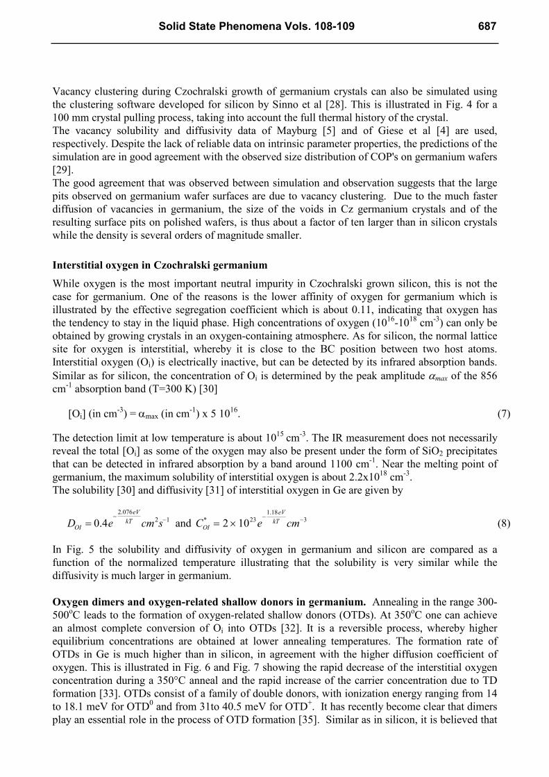
Vacancy clustering during Czochralski growth of germanium crystals can also be simulated using
the clustering software developed for silicon by Sinno et al [28]. This is illustrated in Fig. 4 for a
100 mm crystal pulling process, taking into account the full thermal history of the crystal.
The vacancy solubility and diffusivity data of Mayburg [5] and of Giese et al [4] are used,
respectively. Despite the lack of reliable data on intrinsic parameter properties, the predictions of the
simulation are in good agreement with the observed size distribution of COP's on germanium wafers
[29].
The good agreement that was observed between simulation and observation suggests that the large
pits observed on germanium wafer surfaces are due to vacancy clustering. Due to the much faster
diffusion of vacancies in germanium, the size of the voids in Cz germanium crystals and of the
resulting surface pits on polished wafers, is thus about a factor of ten larger than in silicon crystals
while the density is several orders of magnitude smaller.
Interstitial oxygen in Czochralski germanium
While oxygen is the most important neutral impurity in Czochralski grown silicon, this is not the
case for germanium. One of the reasons is the lower affinity of oxygen for germanium which is
illustrated by the effective segregation coefficient which is about 0.11, indicating that oxygen has
the tendency to stay in the liquid phase. High concentrations of oxygen (1016-10
18 cm
-3) can only be
obtained by growing crystals in an oxygen-containing atmosphere. As for silicon, the normal lattice
site for oxygen is interstitial, whereby it is close to the BC position between two host atoms.
Interstitial oxygen (Oi) is electrically inactive, but can be detected by its infrared absorption bands.
Similar as for silicon, the concentration of Oi is determined by the peak amplitude αmax of the 856 cm
-1 absorption band (T=300 K) [30]
[Oi] (in cm-3) = αmax (in cm
-1) x 5 10
16. (7)
The detection limit at low temperature is about 1015 cm
-3. The IR measurement does not necessarily
reveal the total [Oi] as some of the oxygen may also be present under the form of SiO2 precipitates
that can be detected in infrared absorption by a band around 1100 cm-1. Near the melting point of
germanium, the maximum solubility of interstitial oxygen is about 2.2x1018 cm
-3.
The solubility [30] and diffusivity [31] of interstitial oxygen in Ge are given by
DOI= 0.4e
−2.076eV
kT cm2s−1 and C
OI
* = 2 ×10²³e−1.18eV
kT cm−3 (8)
In Fig. 5 the solubility and diffusivity of oxygen in germanium and silicon are compared as a
function of the normalized temperature illustrating that the solubility is very similar while the
diffusivity is much larger in germanium.
Oxygen dimers and oxygen-related shallow donors in germanium. Annealing in the range 300-
500oC leads to the formation of oxygen-related shallow donors (OTDs). At 350
oC one can achieve
an almost complete conversion of Oi into OTDs [32]. It is a reversible process, whereby higher
equilibrium concentrations are obtained at lower annealing temperatures. The formation rate of
OTDs in Ge is much higher than in silicon, in agreement with the higher diffusion coefficient of
oxygen. This is illustrated in Fig. 6 and Fig. 7 showing the rapid decrease of the interstitial oxygen
concentration during a 350°C anneal and the rapid increase of the carrier concentration due to TD
formation [33]. OTDs consist of a family of double donors, with ionization energy ranging from 14
to 18.1 meV for OTD0 and from 31to 40.5 meV for OTD
+. It has recently become clear that dimers
play an essential role in the process of OTD formation [35]. Similar as in silicon, it is believed that
Solid State Phenomena Vols. 108-109 687

every next family member is formed by attachment of an additional oxygen atom. Hereby the
ionization energies become shallower, the larger the cluster is. In other words, the early members
correspond to the deeper states and vice versa.
At the same temperature both the solubility
and the diffusivity of oxygen are much higher
in germanium than in silicon. This might be a
concern when germanium layers are in contact
with a CZ silicon substrate or with oxide
layers during thermal processing. Due to the
higher solubility and diffusivity, germanium
layers will getter oxygen that might give rise
to TD formation during low temperature
treatments or even during device operation.
Fig. 5: Solubility and diffusivity of interstitial
oxygen in germanium and silicon, normalized
with respect to the melting temperature Tm.
Precipitation of oxygen. Interstitial oxygen precipitation in silicon has been studied for nearly half
a century now due to its important impact on material and device properties. Despite the vast
amount of data and analyses available a number of open questions still remain. It is for instance not
yet unambiguously determined what oxide phase is formed nor is the behavior of interstitial oxygen
well understood over the whole anneal temperature range. The quantitative prediction of oxide
precipitate nucleation and its dependence on the history of the material remains a difficult task.
Similar as for silicon, in germanium that is doped with oxygen from the melt up to its solubility,
interstitial oxygen will precipitate during subsequent thermal treatments in the range between 450
and 650°C. This process leads to the formation of germanium oxide precipitates (GeOx) that can be
observed by their typical absorption bands in FTIR spectra. This is illustrated in Fig. 8 showing the
typical spectrum observed after a thermal treatment of a germanium sample with an initial oxygen
content of 2.5 1017 cm
-3. Before the precipitation anneal, the interstitial oxygen concentration was
maximised by performing an oxygen dissolution treatment at 900°C for 5 min in order to dissolve
all oxygen clusters including thermal donors that were formed during crystal growth, followed by a
rapid quench to room temperature using nitrogen gas cooling. Similar as in silicon a shoulder
develops on the interstitial oxygen absorption band which is due to the formation of a germanium
oxide phase. A typical feature is also the presence of a band around 1100 cm-1 that can be attributed
to SiOx precipitates originating from dissolved silicon. As SiO2 is stable at the germanium melt
temperature, these silicon oxide clusters are formed already during crystal growth [30].
Using the technique developed by De Gryse et al [36] for SiOx precipitates in silicon, it is possible
to determine the shape and phase of the GeOx precipitates in annealed oxygen doped germanium.
Fig. 9 shows a simulated GeOx precipitate spectrum superimposed on the experimental one.
Acknowledgement
This work was supported by the Institute for the Promotion of Innovation by Science and
Technology in Flanders (IWT-Vlaanderen) and the Fund for Scientific Research-Flanders (FWO-
Vlaanderen).
688 Gettering and Defect Engineering in Semiconductor Technology XI

Fig. 6: Oi concentration in oxygen doped Ge vs.
annealing conditions [33,34].
Fig. 7: Carrier concentration in oxygen doped
germanium vs. annealing conditions [33,34].
Fig. 8: Typical infrared absorption spectrum revealing
SiOx and GeOx precipitates in oxygen doped
germanium after a heat treatment for 66h at 610°C
followed by 66h at 560°C [34].
Fig. 9: Absorption spectrum of GeOx
precipitates in oxygen doped germanium
with superimposed a simulated spectrum
assuming polyhedral precipitates [34].
References
[1] http://substrates.umicore.com
[2] J. Vanhellemont, O. De Gryse, S. Hens, P. Vanmeerbeek, D. Poelman, P. Clauws, E. Simoen,
C. Claeys, I. Romandic, A. Theuwis, G. Raskin, H. Vercammen and P. Mijlemans: Defect and
Diffusion Forum 230-232 (2004), p. 149
[3] A. Seeger and K.P. Chik: phys. stat. sol. 19 (1968), p. 455
[4] A. Giese, N.A. Stolwijk and H. Bracht: Appl. Phys. Lett. 77 (2000), p. 642
[5] S. Mayburg: Phys. Rev. 95 (1954), p. 38
[6] A.G. Tweet: Phys. Rev. 106 (1957), p. 221
Solid State Phenomena Vols. 108-109 689

[7] T.V. Mashovets: Sov. Phys. Semicond. 16 (1982), p. 1
[8] N. Bernstein, M. J. Mehl, D. A. Papaconstantopoulos: Phys. Rev. B 66 (2002), p. 075212
[9] Antônio J.R. da Silva, A. Janotti, A. Fazzio, R.J. Baierle and R. Motta: Phys. Rev. B 62 (2000),
p. 9903
[10] F.H. Stillinger and T.A. Weber: Phys. Rev. B 31 (1982), p. 5262
[11] H.R. Schober: Phys. Rev. B 39 (1989), p.13013
[12] T. Sinno: Ph.D. Thesis, Massachusetts Institute of Technology, Cambridge, MA, 1998
[13] A. Fazzio, A. Janotti, Antônio J.R. da Silva and R. Motta: Phys. Rev. B 61 (2000), p. R2401
[14] W. Frank, N.A. Stolwijk: Mater. Sci. Forum 15-18 (1987), p. 369
[15] H.D. Fuchs, W. Walukiewicz, E.E. Haller, W. Dondl, R. Schorer, G. Abstreiter, A.I. Rudnev,
A.V. Tikhomirov, V.I Ozhogin: Phys. Rev. B 51 (1995), p. 16 817
[16] F. Bailly: in Lattice Defects in Semiconductors (ed. by R.R. Hasiguti),University of Tokyo
Press, Tokyo (1968), p. 231
[17] R. A. Swalin: J. Phys. Chem. Solids 18 (1961), p. 290
[18] K.H. Bennemann: Phys. Rev. 137 (1965), p. A1497
[19] A. Scholz and A. Seeger: Phys. Status Solidi 3 (1963), p. 1480
[20] T. Soma, M. Saeki, and A. Morita: J. Phys. Soc. Jpn. 35 (1973), p.146
[21] J.C. Philips and J.A. Van Vechten: Phys. Rev. Lett. 30 (1973), p. 220
[22] R.R. Hasiguti: J. Phys. Soc. Jpn. 21 (1966), p.1927
[23] V.A. Panteleev: Fiz. Tverd. Tela (Leningrad) 19 (1977), p. 2801 [in Russian]
[24] V.I. Okulich: Author’s Abstract of Thesis for Candidate’s Degree, State University, Gorki
(1964) [in Russian]
[25] V.V. Voronkov and R. Falster: Journ Electrochem. Soc. 149 (2002), p. G167
[26] J. Vanhellemont: J. Appl. Phys. 78 (1995), p. 4297
[27] J. Vanhellemont: Appl. Phys. Lett. 69 (1996), p. 4008
[28] T. Sinno, E. Dornberger, W. von Ammon, R.A. Brown and F. Dupret: Material Science and
Engineering 28 (2000), p. 149
[29] S. Hens, J. Vanhellemont, D. Poelman, P. Clauws, I. Romandic, F. Holsteyns and J. Van
Steenbergen: submitted for publication in Applied Physics Letters.
[30] W. Kaiser and C.D. Thurmond: J. Appl. Phys. 32 (1961), p. 115
[31] J.W. Corbett, R.S. Mc Donald and D.G. Watkins: J. Phys. Chem. Solids 25 (1964), p. 873
[32] P. Clauws: Mater. Sci. Eng. B 36 (1996), p. 213
[33] P. Vanmeerbeek: PhD thesis, Ghent University (2004).
[34] M. De Bock: Master thesis, Ghent University (2002).
[35] P. Vanmeerbeek, P. Clauws and W. Mondelaers: Physica B 308-310 (2001), p. 517
[36] O. De Gryse, P. Clauws, J. Van Landuyt, O. Lebedev, C. Claeys, E. Simoen and J.
Vanhellemont: J. Appl. Phys. 91 (2002), p. 2493
690 Gettering and Defect Engineering in Semiconductor Technology XI

Gettering and Defect Engineering in Semiconductor Technology XI 10.4028/www.scientific.net/SSP.108-109 Recent Progress in Understanding of Lattice Defects in Czochralski-Grown Germanium: Catching-up
with Silicon 10.4028/www.scientific.net/SSP.108-109.683
DOI References
[2] J. Vanhellemont, O. De Gryse, S. Hens, P. Vanmeerbeek, D. Poelman, P. Clauws, E. Simoen, . Claeys, I.
Romandic, A. Theuwis, G. Raskin, H. Vercammen and P. Mijlemans: Defect and iffusion Forum 230-232
(2004), p. 149
doi:10.4028/www.scientific.net/DDF.230-232.149 [6] A.G. Tweet: Phys. Rev. 106 (1957), p. 221
doi:10.1103/PhysRev.106.221 [9] Antônio J.R. da Silva, A. Janotti, A. Fazzio, R.J. Baierle and R. Motta: Phys. Rev. B 62 (2000), . 9903
doi:10.1103/PhysRevB.62.9903 [14] W. Frank, N.A. Stolwijk: Mater. Sci. Forum 15-18 (1987), p. 369
doi:10.4028/www.scientific.net/MSF.15-18.369 [18] K.H. Bennemann: Phys. Rev. 137 (1965), p. A1497
doi:10.1103/PhysRev.137.A1497 [28] T. Sinno, E. Dornberger, W. von Ammon, R.A. Brown and F. Dupret: Material Science and ngineering
28 (2000), p. 149
doi:10.1016/S0927-796X(00)00015-2 [31] J.W. Corbett, R.S. Mc Donald and D.G. Watkins: J. Phys. Chem. Solids 25 (1964), p. 873
doi:10.1016/0022-3697(64)90100-3 [32] P. Clauws: Mater. Sci. Eng. B 36 (1996), p. 213
doi:10.1016/0921-5107(95)01255-9 [36] O. De Gryse, P. Clauws, J. Van Landuyt, O. Lebedev, C. Claeys, E. Simoen and J. anhellemont: J. Appl.
Phys. 91 (2002), p. 2493
doi:10.1088/0953-8984/14/48/367 [2] J. Vanhellemont, O. De Gryse, S. Hens, P. Vanmeerbeek, D. Poelman, P. Clauws, E. Simoen, C. Claeys,
I. Romandic, A. Theuwis, G. Raskin, H. Vercammen and P. Mijlemans: Defect and Diffusion Forum 230-232
(2004), p. 149
doi:10.4028/www.scientific.net/DDF.230-232.149 [9] Antnio J.R. da Silva, A. Janotti, A. Fazzio, R.J. Baierle and R. Motta: Phys. Rev. B 62 (2000), p. 9903
doi:10.1103/PhysRevB.62.9903 [13] A. Fazzio, A. Janotti, Antnio J.R. da Silva and R. Motta: Phys. Rev. B 61 (2000), p. R2401
doi:10.1103/PhysRevB.61.R2401 [15] H.D. Fuchs, W. Walukiewicz, E.E. Haller, W. Dondl, R. Schorer, G. Abstreiter, A.I. Rudnev, A.V.
Tikhomirov, V.I Ozhogin: Phys. Rev. B 51 (1995), p. 16 817
doi:10.1103/PhysRevB.51.16817 [28] T. Sinno, E. Dornberger, W. von Ammon, R.A. Brown and F. Dupret: Material Science and Engineering
28 (2000), p. 149

doi:10.1016/S0927-796X(00)00015-2 [36] O. De Gryse, P. Clauws, J. Van Landuyt, O. Lebedev, C. Claeys, E. Simoen and J. Vanhellemont: J.
Appl. Phys. 91 (2002), p. 2493
doi:10.1063/1.1429800
Related Documents