This is a repository copy of Real-time Measurement of Temperature Sensitive Electrical Parameters in SiC Power MOSFETs. White Rose Research Online URL for this paper: http://eprints.whiterose.ac.uk/118921/ Version: Accepted Version Article: Griffo, A. orcid.org/0000-0001-5642-2921, Wang, J., Colombage, K. et al. (1 more author) (2017) Real-time Measurement of Temperature Sensitive Electrical Parameters in SiC Power MOSFETs. IEEE Transactions on Industrial Electronics. ISSN 0278-0046 https://doi.org/10.1109/TIE.2017.2739687 © 2017 IEEE. Personal use of this material is permitted. Permission from IEEE must be obtained for all other users, including reprinting/ republishing this material for advertising or promotional purposes, creating new collective works for resale or redistribution to servers or lists, or reuse of any copyrighted components of this work in other works. [email protected] https://eprints.whiterose.ac.uk/ Reuse Items deposited in White Rose Research Online are protected by copyright, with all rights reserved unless indicated otherwise. They may be downloaded and/or printed for private study, or other acts as permitted by national copyright laws. The publisher or other rights holders may allow further reproduction and re-use of the full text version. This is indicated by the licence information on the White Rose Research Online record for the item. Takedown If you consider content in White Rose Research Online to be in breach of UK law, please notify us by emailing [email protected] including the URL of the record and the reason for the withdrawal request.

Welcome message from author
This document is posted to help you gain knowledge. Please leave a comment to let me know what you think about it! Share it to your friends and learn new things together.
Transcript

This is a repository copy of Real-time Measurement of Temperature Sensitive Electrical Parameters in SiC Power MOSFETs.
White Rose Research Online URL for this paper:http://eprints.whiterose.ac.uk/118921/
Version: Accepted Version
Article:
Griffo, A. orcid.org/0000-0001-5642-2921, Wang, J., Colombage, K. et al. (1 more author) (2017) Real-time Measurement of Temperature Sensitive Electrical Parameters in SiC Power MOSFETs. IEEE Transactions on Industrial Electronics. ISSN 0278-0046
https://doi.org/10.1109/TIE.2017.2739687
© 2017 IEEE. Personal use of this material is permitted. Permission from IEEE must be obtained for all other users, including reprinting/ republishing this material for advertising orpromotional purposes, creating new collective works for resale or redistribution to servers or lists, or reuse of any copyrighted components of this work in other works.
[email protected]://eprints.whiterose.ac.uk/
Reuse
Items deposited in White Rose Research Online are protected by copyright, with all rights reserved unless indicated otherwise. They may be downloaded and/or printed for private study, or other acts as permitted by national copyright laws. The publisher or other rights holders may allow further reproduction and re-use of the full text version. This is indicated by the licence information on the White Rose Research Online record for the item.
Takedown
If you consider content in White Rose Research Online to be in breach of UK law, please notify us by emailing [email protected] including the URL of the record and the reason for the withdrawal request.
IEEE TRANSACTIONS ON INDUSTRIAL ELECTRONICS
1 Abstract— This paper examines a number of techniques
for junction temperature estimation of SiC MOSFETs devices based on the measurement of Temperature Sensitive Electrical Parameters (TSEPs) for use in online condition monitoring. Linearity, sensitivity to temperature and circuit design for practical implementation are discussed in detail. A demonstrator based on the measurement of the quasi-threshold voltage, the turn-on transient characteristic (di/dt), the on-state voltage and the gate current peak is designed and validated. It is shown that the threshold voltage, the estimation of the gate current peak and the on-state voltage have potentially good sensitivity to temperature variation and linearity over a wide operating range. Very low sensitivity to temperature is shown for (di/dt). The proposed method can provide a valuable tool for continuous health monitoring in emerging applications of SiC devices to high reliability applications.
Index Terms—Power semiconductor devices, Condition monitoring, Power MOSFETs, Temperature measurements
I. INTRODUCTION
OWER electronic systems play an increasingly significant role in high reliability applications such as the automotive
and aerospace sectors. However, stringent safety requirements and conservative design practices pose significant challenges to the adoption of novel and relatively unproven technologies such as the use of novel wide band-gap (WBG) devices e.g. Silicon Carbide (SiC) power MOSFETs or Gallium Nitride (GaN) high electron mobility transistors which have the potential to significantly increase efficiency and power density. Continuous condition monitoring of power devices can potentially reduce failure rates and alleviate reliability concerns by providing real-time information on the state of health of the devices and indication on the remaining useful lifetime [1]-[2].
Reliability of power electronic components is significantly affected by the device operating conditions. It is well known that two of the most significant stress factors for power electronics modules are absolute temperature and temperature variations which result in thermo-mechanical stress due the different coefficients of thermal expansions (CTEs) of materials in the modules [3]-[4]. Repetitive thermal cycling can eventually cause cracks and voids in solder joints, bond-wire lift-off, and delamination within module interconnection
1 Manuscript received March 21, 2017; revised May 17, 2017; accepted July
5, 2017. This work was supported by European Commission Horizon 2020 – Mobility for Growth Program, under Grant 636170. A. Griffo, J. Wang and T. Kamel are with the Department of Electronic and Electrical Engineering, The
resulting in increased thermal resistance and ultimately even higher junction temperatures [5].
The measurement or estimation of junction temperature during the operation of a power electronic converter is therefore essential for its condition monitoring and prognosis of the remaining useful life [6].
Monitoring of devices junction temperatures during real-time operation of a power electronics converter can be realized with either direct or indirect methods [7]. Direct temperature measurements using optical or physical contact methods have been proposed in literature [8]-[9]. Optical methods using optical fibers [8] and infrared thermal imaging can provide an accurate spatial temperature map of the power electronic module. However, these methods require the chip to be optically connected to the detection system and therefore the protective dielectric gel has to be removed. Similarly, physical contact methods require a direct contact with the chip with a thermo-sensitive material [9] or temperature probes requiring significant alterations to module packaging and dielectric gel. Whilst potentially the most accurate ways of monitoring temperature, the invasive nature of direct measurement methods make them only suitable in laboratory testing conditions and therefore unsuitable for general applications.
It is well known that a number of electrical parameters in semiconductor devices exhibit a measurable temperature dependence. The measurement of Temperature Sensitive Electric Parameters (TSEPs) can potentially provide a more practical, albeit indirect, solution for temperature monitoring of power devices [10]-[13]. The non-invasive nature of TSEPs-based approaches can allow temperature estimation on standard packaged modules without modification to the module itself, only requiring access to terminal electrical quantities.
A number of studies have been published on the use of TSEPs for Silicon (Si) MOSFETs and IGBTs power devices, including the monitoring of dI/dt during turn-on or dV/dt during turn-off transients [14]-[16], Miller capacitance discharge time [17], threshold voltage [18]-[20], on-state voltage drop [21]-[23], voltage across source/emitter parasitic inductance [24], internal gate resistance [25]-[26], gate drive turn-on transients [27].
Despite the increased interest in the use of WBG devices, only very limited literature is available in the public domain on the use of TSEPs for SiC MOSFETs [28]-[29]. Furthermore, most of the publications on TSEPs focus on the description of the underlying physical properties and often do not provide
University of Sheffield, S1 4DE, Sheffield, U.K. (e-mail: [email protected]). Kalhana Colombage is with Malvern Instruments, Ltd., Malvern WR14 1XZ, U.K.
Real-time Measurement of Temperature Sensitive Electrical Parameters in SiC
Power MOSFETs Antonio Griffo, Member, IEEE, Jiabin Wang, Senior Member, IEEE, Kalhana Colombage,
Tamer Kamel, Member, IEEE
P
IEEE TRANSACTIONS ON INDUSTRIAL ELECTRONICS
circuit design guidelines for practical implementation of TSEPs measurement in a real-time condition monitoring system.
The paper presents an overview of the methods for junction temperature estimation based on the measurement of TSEPs and discusses the feasibility of online monitoring of TSEPs of SiC MOSFET devices. Four potential TSEPs are identified, namely the quasi-threshold voltage, the turn-on transient (di/dt) characteristic, the on-state voltage and the gate current peak, based on sensitivity to temperature and suitability for online measurement under converter switching operation. Comprehensive design and experimental validation of the proposed online monitoring techniques are presented.
II. TEMPERATURE SENSITIVE ELECTRIC PARAMETERS IN SIC MOSFETS
The temperature dependence of the electrical characteristics of semiconductor devices arises as a result of the thermal dependency of a number of parameters, the most significant being the bandgap energy 継直岫劇岻┸ the effective mobility 航岫劇岻 and intrinsic concentration 券沈岫劇岻 of the charge carriers. Similarly to most semiconductor materials, the bandgap energy 継直岫劇岻 decreases as temperature increases, whilst the intrinsic concentration increases with temperature [30]. The mobility 航岫劇岻 in SiC devices has a more complex dependency on temperature depending on doping levels and density of traps at the gate oxide/SiC interface resulting in bulk mobility to decrease but channel mobility to potentially increase with temperature [31]-[32]. Temperature effects on these parameters can be summarised by the empirical relations: 継直岫劇岻 噺 継直岫劇待岻 伐 糠怠 劇態劇 髪 紅怠 (1)
券沈岫劇岻 噺 軽底鉄 exp 岾伐 紘劇峇 (2)
航岫劇岻 噺 航待 紅態 岾 劇劇待峇底典な 髪 紅態 岾 劇劇待峇底填 (3)
where 糠沈 ┸ 紅沈 ┸ 紘 are fitting coefficients. As a consequence, most terminal device characteristics are temperature dependent.
The sensitivity to temperature rise of on-state resistance, threshold voltage 撃痛朕, drain current commutation rate 穴荊帖聴【穴建 and gate current Miller plateau are evaluated through analytical modelling and experimental measurements on SiC MOSFETs and compared to those of Si IGBTs in [29]. A general conclusion is that the use of TSEPs in SiC devices is relatively more challenging than in Si IGBT. This is due to faster switching transients and lower sensitivity to temperature which are caused by the wider band-gap requiring more thermal energy to excite charge carriers as well as smaller chip areas resulting in lower Miller capacitance.
The on-state voltage 撃帖聴┸墜津, threshold voltage 撃痛朕, the internal gate resistance (迎弔┸沈津痛) indirectly estimated by measuring the peak of gate current and the turn-on transient 岫穴件帖聴【穴建岻 have been selected for further analyses based on their suitability for online measurement under converter switching operation.
A. On-state voltage 撃帖聴┸墜津
The on-state resistance 迎帖聴┸墜津 and consequently the voltage across the device during forward conduction 撃帖聴┸墜津 have a reasonably good sensitivity to temperature as shown in the measurements in Fig. 1. However, the temperature dependence is potentially nonlinear and current-dependent, therefore its use in online monitoring requires current measurement in order to decouple the load dependency from thermal effects. 撃帖聴┸墜津 is also dependent on the state-of-health of device-to-packaging interconnects and indeed the collector-emitter voltage 撃寵帳 in IGBTs has also been proposed as a condition monitoring indicator of wirebond lift-off and solder fatigue [33].
The main challenge in the practical use of the 撃帖聴┸墜津 for online monitoring resides on the significant voltage excursion across drain-source terminals during converter switching, ranging from few Volts during conduction to well over the dc-link voltage 撃鳥頂 during turn-off transients. These voltage excursions complicate the design of signal acquisition circuitry with significant challenges in terms of high dynamic range and isolation between the low-voltage monitoring circuit and the high-voltage power stage. A number of circuits suitable for on-state voltage measurement derived from commonly used methods for de-saturation protection have been proposed using either passive (diode) or active solutions for disconnecting the measurement circuitry during turn-off transients [22]. The emitter-follower circuit illustrated in Fig. 1 shows a practical solution to the measurement of 撃帖聴┸墜津 of the device 警な under test [21]. The device 警に isolates the measuring circuitry connected to 撃陳 from the high voltage side when the drain 経 voltage rises above the reference ひ撃 during turn-off transient of M1, effectively limiting 撃陳 to safe voltage levels. When the device M1 under test is switched on, 撃帖聴┸墜津is a few volts, and M2 is heavily saturated. Hence the measurement voltage 撃陳 across 迎 is effectively equal to 撃帖聴┸墜津. When M1 is switched off, 撃帖聴 quickly increases to the DC link voltage. As soon as 撃帖聴 raises above 9撃┸ the gate-source voltage of M2 drops to zero effectively switching M2 off, isolating the measurement point from the high voltage. With this circuit, the voltage measurement range is reduced to a few volts, and hence accuracy and resolution can be significantly improved.
Fig. 1. Circuit schematic for 惨拶傘┸伺仔 measurement
B. Threshold voltage 惨嗣酸
The threshold voltage 撃痛朕 is the minimum gate-source voltage required to switch on the device. Physically, 撃痛朕 is the minimum gate bias starting to induce an inversion layer of free electrons underneath the gate oxide, creating a conductive channel between drain and source in MOSFET or collector and emitter in IGBT. The increase of carrier concentration and the decrease of bandgap with temperature results in a decrease of

IEEE TRANSACTIONS ON INDUSTRIAL ELECTRONICS
撃痛朕 with temperature, typically modelled as an approximately linear dependence. Practical measurement of 撃痛朕 ┸ such as those reported in datasheets, requires the definition of a current level at which the gate measurement is taken. Although, current comparison can be effectively used in static conditions, similarly to those used in datasheet measurements, it is not practical for online measurements during switching transients.
Fig. 2. Schematic circuit for quasi-threshold voltage measurement
The main challenge in online detection of 撃痛朕 during turn-on transients lies in the sampling of the gate voltage at the correct instant in time since the gate-source voltage 撃直鎚 has very fast rising times typically up to な撃【券嫌. A potentially suitable method used for the detection of a quasi-threshold voltage, adapted from [19],[34] where it was proposed for IGBT applications, is illustrated in Fig. 2. A voltage across the parasitic inductance between the auxiliary Kelvin source (S’) and the source (S) is generated when the device current 件帖聴 starts to rise during device turn-on. The rising edge of the voltage 懸聴聴嫦 across the parasitic inductance, which is proportional to 穴件帖聴【穴建, can be used to trigger the sample and hold circuitry acquiring the gate-source voltage 懸弔聴嫗 effectively capturing the start of conduction and therefore the quasi-threshold voltage. An AND gate activated by the gate drive signal, is used to avoid spurious triggering due to noise outside of the switching transients. Illustrative waveforms of the gate drive signal, gate-source voltage 懸弔聴嫗, voltage across the external gate resistance 撃眺弔 and the voltage across the parasitic inductance 懸聴聴嫦 during a turn-on event, are shown Fig. 3.
A potentially significant benefit of 撃痛朕 use as TSEP is its independence from load current. C. Internal gate resistance (RG,in)
The internal gate resistance 迎弔┸沈津痛 is the lumped equivalent of the distributed resistance of the polysilicon gate and metal contacts in the MOSFET device. From terminal point of view, 迎弔┸沈津痛 can be considered in series with the parallel of the gate-source and gate-drain capacitances. The time constant 酵墜津 of the equivalent gate capacitance charging process during turn-on before 撃痛朕 is reached can be expressed as: 酵墜津 噺 盤迎弔┸勅掴 髪 迎弔┸沈津痛匪盤系弔聴 髪 系弔帖岫撃帖聴岻匪 (4)
where 迎弔┸勅掴 is the external gate resistance , 系弔聴 and 系弔帖 are the gate-source and gate-drain capacitances, respectively. At turn-on, for a fixed DC-link voltage, the drain-source voltage 撃帖聴
can be considered constant, hence 系弔帖 can also be considered
Fig. 3. Typical waveforms during SiC MOSFET (CCS020M12CM2) turn-on transient: gate drive signal, gate-source voltage 惨札傘, voltage across the external gate resistance 惨三札 (top) and the voltage across the parasitic inductance 惨傘傘嫦 (bottom). constant. 系弔聴 does not change significantly until 撃痛朕 is reached. 迎弔┸勅掴 is assumed to be constant at a known ambient temperature. It follows that 迎弔┸沈津痛 becomes the dominating temperature dependant parameter in (4) affecting gate current during turn-on. Assuming the simplified 迎系 circuit representation of gate charging process, the peak of the gate current 件弔 can be considered proportional to 迎弔┸沈津. A simple peak detector circuit measuring the voltage across the external gate resistor (撃眺弔┸勅掴痛) whose peak is directly proportional to the gate current [25]-[27], is outlined in the schematic shown in Fig. 4.
Similarly to 撃痛朕, the internal gate resistance as TSEP is potentially load independent. Heavy doping of polysilicon required for low resistivity gates, typically results in low temperature coefficient of its resistivity [35], potentially resulting in low sensitivity of 迎弔┸沈津 as a TSEP.
Fig. 4. Schematic circuit for gate current peak detection D. Turn-on transient 岫穴件帖聴【穴建岻
The rate of change of device current 件帖聴 during a turn-on transient can be expressed as [28]:
IEEE TRANSACTIONS ON INDUSTRIAL ELECTRONICS
穴件帖聴穴建噺 航 系墜掴激詣 岫撃弔聴 伐 撃痛朕岻 撃弔弔迎弔岫系弔聴 髪 系弔帖岻 結貸 痛眺奈岫寵奈縄袋寵奈呑岻 (5)
where 航 is the electron mobility, 系墜掴 is the intrinsic gate oxide capacitance, 激【詣 is the gate width/length ratio, 撃弔弔 is the gate drive voltage.
The negative temperature coefficient of both threshold voltage 撃痛朕 and mobility 航 have contrasting influence on 穴件帖聴【穴建. While a reduction in 撃痛朕 with temperature would favour faster turn-on, the reduction of mobility would have opposite influence on 穴件帖聴【穴建. As a first order approximation, the temperature dependency of 航 could be neglected in the initial phase of the turn-on process, resulting in the prediction of increase of 穴件帖聴【穴建 with temperature. Extensive measurements reported in [29] shows that the temperature variation of 穴件帖聴【穴建 is device and circuit dependent. For large devices 穴件帖聴【穴建 increases with temperature, however the variation becomes very small for low current devices. The gate drive resistance 迎直 also has a strong influence on 穴件帖聴【穴建 and its sensitivity to temperature variations becomes vanishingly small for low values of 迎直 required for switching losses minimization. Gate drives with variable output resistances have been proposed as a potential solution for occasional temperature monitoring [18]. In conclusion, the practical use of 穴件帖聴【穴建 as TSEP is non-trivial not only because of the extremely fast transients resulting in challenging acquisition circuit design, but also due to a potentially very low temperature sensitivity and current dependence.
Since the voltage 撃聴聴嫦 across the source parasitic inductance 詣聴聴嫦 is proportional to the rate of change of 件帖聴, the peak value of 撃聴聴嫦 will be used as an indirect measurement of 穴件帖聴【穴建 as illustrated in Fig. 5. The peak detector can be realised with a precision half-wave rectifier, a circuit also known as active diode, and a resettable memory capacitor as shown in Fig. 6. The memory capacitor hold the peak value of the voltage across 詣聴聴嫦 over the turn-on transient until is reset in the next switching cycle. The integration of 撃聴聴嫦 can be used to estimate the output current 件帖聴 as illustrated in Fig. 7. This can provide a practical way of estimating device current which can be used to decouple load and temperature dependence of the proposed TSEPs.
Fig. 5. Schematic circuit for measurement of peak voltage and current across 鯖傘傘嫦
Fig. 6. Schematic circuit for peak detector
Fig. 7. Current measurement using integration of 惨傘傘嫦 A qualitative comparison of the analysed TSEPs for SiC
MOSFETs is summarized in Tab. 1.
TABLE I COMPARISON OF TSEPS FOR SIC MOSFETS
TSEP ADVANTAGES DISADVANTAGES
On-state
voltage
drop (惨拶傘)
Good potential
sensitivity
No modification to
module
Not linear in SiC
Current dependent
Small value and less
sensitive to temperature
variation in SiC
Non-trivial circuit isolation
Threshold
voltage
(惨嗣酸)
On-line monitoring
possible via an
auxiliary Kelvin source
and parasitic
inductance
An auxiliary Kelvin source is
required
Less temperature sensitive
in SiC
Susceptible to noise
Turn-off
and Turn-
on times or 纂餐【纂嗣
On-line monitoring
possible via an
auxiliary Kelvin
source and parasitic
inductance
Low temperature sensitivity
High dI/dt or short duration
Complex behaviour in SiC
Internal
Gate
Resistance/
current
No module
modification is
required, possible also
on three-terminal
devices (without
auxiliary Kelvin
source)
High resolution ADC is
required
Susceptible to noise
III. TSEPS MONITORING CIRCUIT DESIGN
The methods for online TSEPs monitoring described in the previous section have been implemented in a data acquisition

IEEE TRANSACTIONS ON INDUSTRIAL ELECTRONICS
and control circuit board whose main functionalities are shown in the block diagram of Fig. 8. Two high resolution (18-bit) Analog-to-Digital Converters (ADC) are at the core of the proposed design. The ADCs, configured with a full differential range of ± 4.096V provide a resolution of 0.031 兼撃. The voltages across the external gate resistance 撃眺直, the voltage between the source and auxiliary source connection 撃聴聴嫦 , the gate-source voltage 撃弔聴嫦 and the voltage across the drain-source 撃帖聴 are all measured on the power SiC MOSFET. An additional channel is dedicated to thermistor (NTC) temperature sensor for module baseplate temperature monitoring purpose. Resettable peak detectors and integrators are used to measure the peak of 撃聴聴嫦 and 撃眺直 during turn-on and integrate 撃聴聴嫦, respectively, as described in the previous sections. A supervisory CPU (ARM Cortex M4) controls the data acquisition communicating with the ADCs and controlling the reset signals for the integration and peak detection, generates the control signals for the gate drives and manages the USB communication interface with a supervisory PC for data storage and display.
Fig. 8. Schematic diagram of the designed aquisition board for TSEPs monitoring
The timing of the control signals is managed by the CPU
depending on the specific TSEP to be measured. The data transfer from ADCs and CPU is through SPI bus and the required physical isolation between the analogue side (referenced to the power converter ground) and the digital side (CPU) is obtained with the use of opto-coupled digital isolator integrated circuits. Photos of the top and bottom sides of the manufactured board, annotated with the main features and components, are shown in Fig. 9. The board, manufactured on a four-layer PCB measures 78mm x 50 mm.
Fig. 9. Top (a) and bottom (b) side of the aquisition board
IV. EXPERIMENTAL SETUP
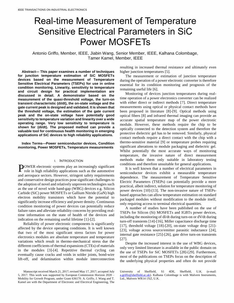
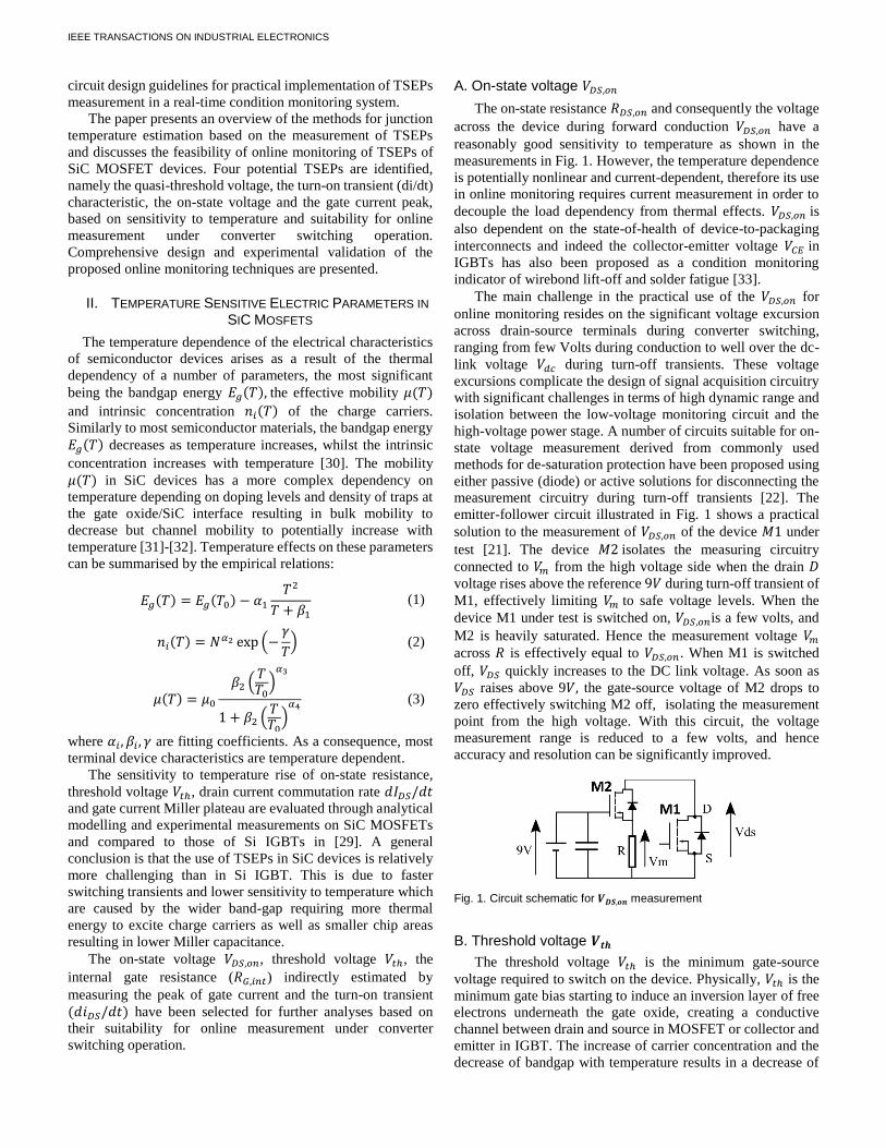
Experimental assessment of the proposed TSEPs monitoring has been performed using a double pulse testing setup whose schematic and principle of operation are illustrated in Fig. 10. A photo of the experimental setup is shown in Fig. 11. An air-cored inductor (なばど航茎) is used as load. A temperature controlled hot-plate is used for testing at different conditions. A SiC six-pack module (Cree CCS020M12CM2) has been used. The module is mounted on PCB providing planar DC link connections. An off-the-shelf gate drive (Prodrive Technologies - PT62SCMD12) has been used. An interface PCB is used to isolate the CPU and the computer through USB interface. Although the ADC PCB also contains digital isolators to isolate the Kelvin source (GND) from the CPU, the digital interface and isolation PCB adds extra protection for the user and the computer. In addition, this PCB also contains a USB to serial bridge (for SPI communication over USB) as well as JTAG connection to the CPU (through external J-Link emulator). The gate drive signal generated by the CPU in the ADC PCB is also routed through this PCB.
(a)
(b)
IEEE TRANSACTIONS ON INDUSTRIAL ELECTRONICS
Fig. 10. Schematic circuit (left) and exemplary waveforms (right) of a double pulse test
Fig. 11. Experimental setup (a) and view of the power module (b)
V. RESULTS AND DISCUSSION
Experimental measurements have been performed on the SiC module up to its maximum rated current (29.5A at 25°C) and at temperatures ranging from ambient to 130°C. Temperature is controlled with the hotplate and monitored through the integrated NTC in the module. If sufficient time is allowed between the application of the double pulse transients, device self-heating is minimized and, in steady-state conditions, the device temperature will be equal to the baseplate temperature measured by the integrated NTC.
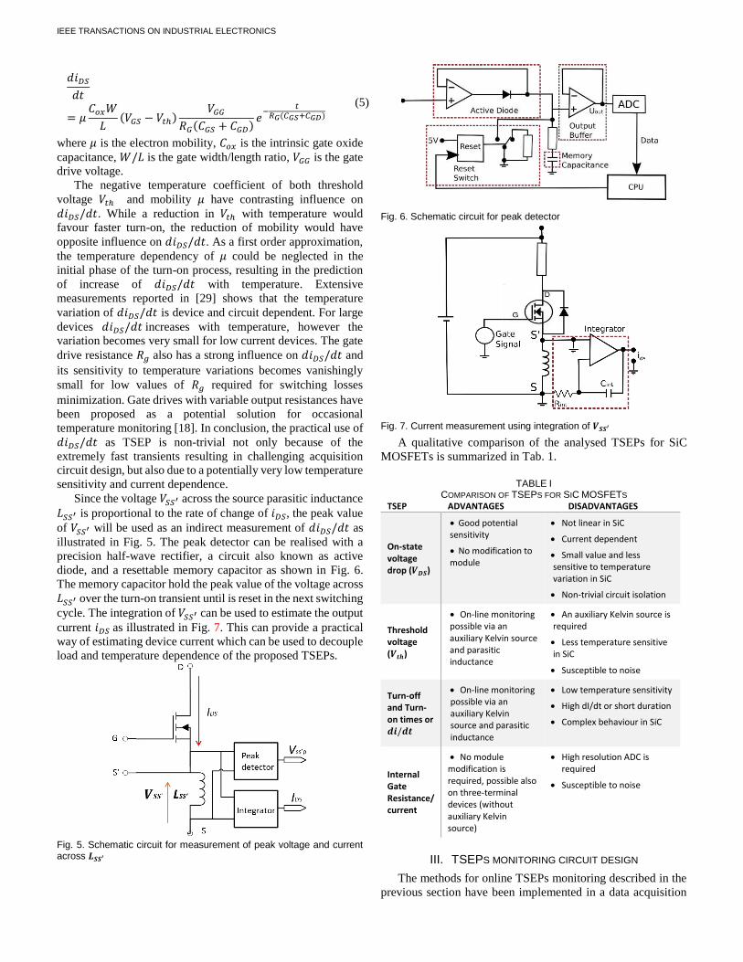
A. On-state voltage 懸帖聴 墜津
The measured on-state voltage 懸帖聴 墜津 as function of temperature and load current with 懸弔聴 噺 にど撃 is shown in Fig. 12. A good sensitivity of なぬ┻ば兼撃【ソ系 at maximum current is demonstrated, similar to the sensitivity of approximately など兼撃【ソ系 reported in the datasheet reported in the device
datasheet using offline methods. A small discrepancy might be due to slightly different testing conditions e.g. gate drive voltage and device variability. A good linearity with temperature is also evident. The on-state voltage is, however, current-dependent and therefore the use of 懸帖聴 墜津 as TSEP requires an independent measurement of device current in order to decouple the load from temperature effects. Device current measurement can be obtained either through resistive shunts or using the integration of parasitic inductance voltage 撃聴聴嫦 as described in the previous section. However a shunt may compromise packaging and add extra loss to converter, both are not desirable.
Fig. 12. Measured on-state voltage 士拶傘 伺仔 as function of temperature and load current
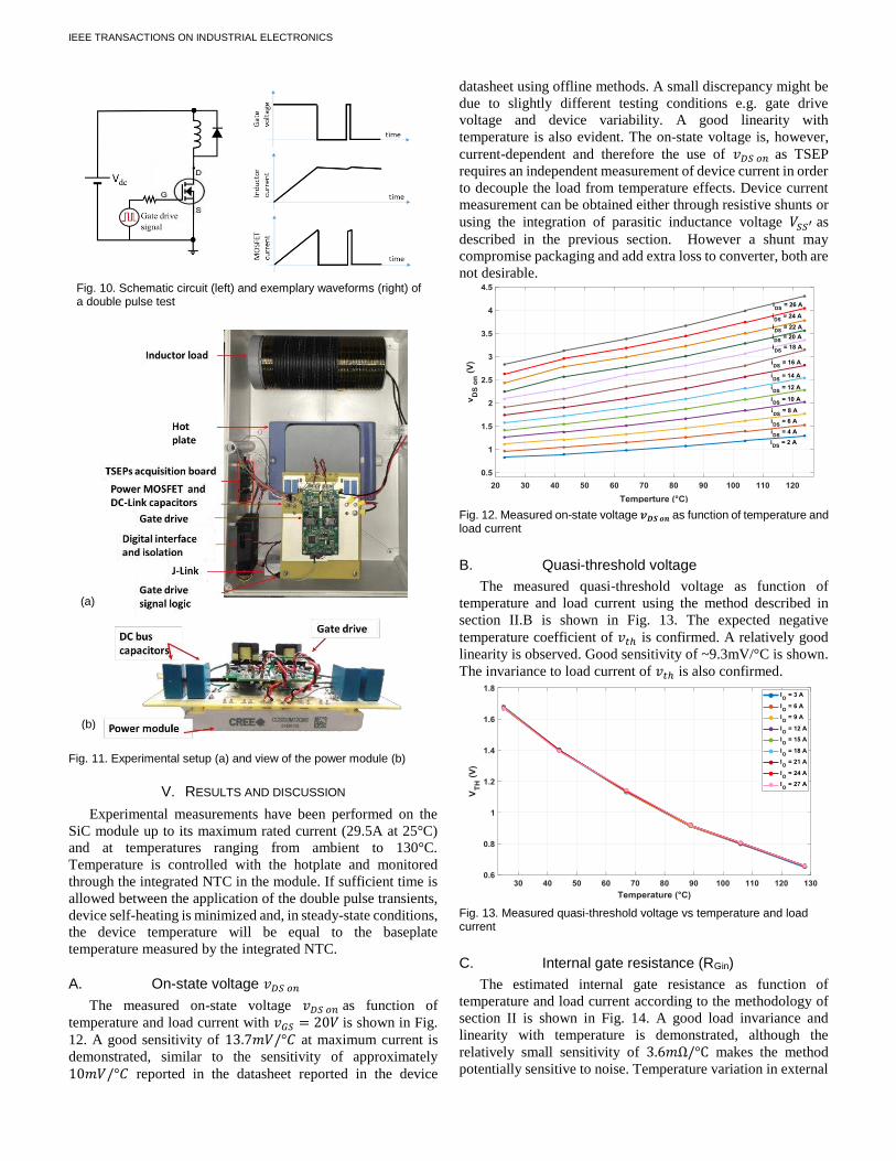
B. Quasi-threshold voltage
The measured quasi-threshold voltage as function of temperature and load current using the method described in section II.B is shown in Fig. 13. The expected negative temperature coefficient of 懸痛朕 is confirmed. A relatively good linearity is observed. Good sensitivity of ~9.3mV/°C is shown. The invariance to load current of 懸痛朕 is also confirmed.
Fig. 13. Measured quasi-threshold voltage vs temperature and load current
C. Internal gate resistance (RGin)
The estimated internal gate resistance as function of temperature and load current according to the methodology of section II is shown in Fig. 14. A good load invariance and linearity with temperature is demonstrated, although the relatively small sensitivity of ぬ┻は兼よ【ソC makes the method potentially sensitive to noise. Temperature variation in external
(a)
(b)
IEEE TRANSACTIONS ON INDUSTRIAL ELECTRONICS
gate resistance and in the gate drive circuit will also affect the accuracy of estimation. Therefore, the external gate resistance should be selected with very low temperature coefficient. The effect of variation of gate drive characteristic with temperature may be decoupled by measurement of the gate voltage.
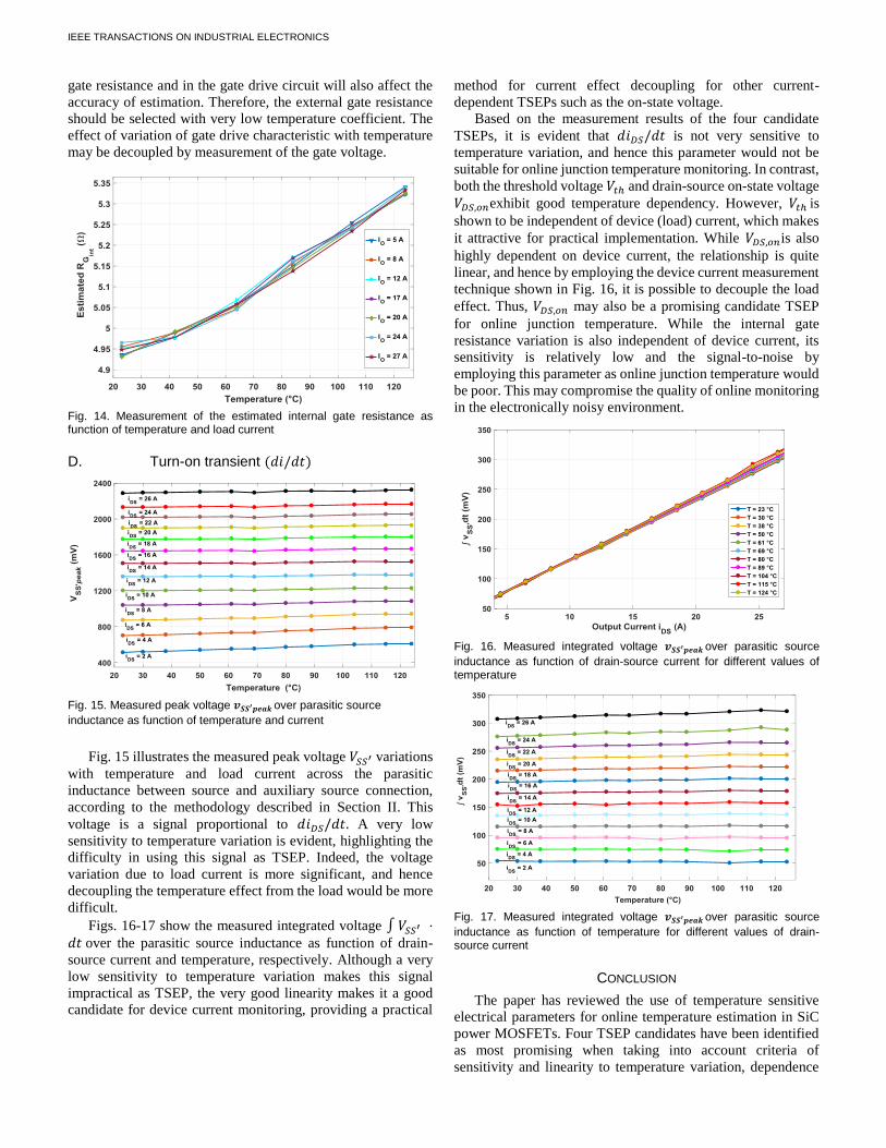
Fig. 14. Measurement of the estimated internal gate resistance as function of temperature and load current D. Turn-on transient 岫穴件【穴建岻
Fig. 15. Measured peak voltage 士傘傘嫦使蚕珊暫 over parasitic source inductance as function of temperature and current
Fig. 15 illustrates the measured peak voltage 撃聴聴嫦 variations
with temperature and load current across the parasitic inductance between source and auxiliary source connection, according to the methodology described in Section II. This voltage is a signal proportional to 穴件帖聴【穴建┻ A very low sensitivity to temperature variation is evident, highlighting the difficulty in using this signal as TSEP. Indeed, the voltage variation due to load current is more significant, and hence decoupling the temperature effect from the load would be more difficult.
Figs. 16-17 show the measured integrated voltage 完 撃聴聴嫦 糾穴建 over the parasitic source inductance as function of drain-source current and temperature, respectively. Although a very low sensitivity to temperature variation makes this signal impractical as TSEP, the very good linearity makes it a good candidate for device current monitoring, providing a practical
method for current effect decoupling for other current-dependent TSEPs such as the on-state voltage.
Based on the measurement results of the four candidate TSEPs, it is evident that 穴件帖聴【穴建 is not very sensitive to temperature variation, and hence this parameter would not be suitable for online junction temperature monitoring. In contrast, both the threshold voltage 撃痛朕 and drain-source on-state voltage 撃帖聴┸墜津exhibit good temperature dependency. However, 撃痛朕 is shown to be independent of device (load) current, which makes it attractive for practical implementation. While 撃帖聴┸墜津is also highly dependent on device current, the relationship is quite linear, and hence by employing the device current measurement technique shown in Fig. 16, it is possible to decouple the load effect. Thus, 撃帖聴┸墜津 may also be a promising candidate TSEP for online junction temperature. While the internal gate resistance variation is also independent of device current, its sensitivity is relatively low and the signal-to-noise by employing this parameter as online junction temperature would be poor. This may compromise the quality of online monitoring in the electronically noisy environment.
Fig. 16. Measured integrated voltage 士傘傘嫦使蚕珊暫 over parasitic source inductance as function of drain-source current for different values of temperature
Fig. 17. Measured integrated voltage 士傘傘嫦使蚕珊暫 over parasitic source inductance as function of temperature for different values of drain-source current
CONCLUSION
The paper has reviewed the use of temperature sensitive electrical parameters for online temperature estimation in SiC power MOSFETs. Four TSEP candidates have been identified as most promising when taking into account criteria of sensitivity and linearity to temperature variation, dependence

IEEE TRANSACTIONS ON INDUSTRIAL ELECTRONICS
on loading conditions as well as practicality in real-time measurement.
Practical circuits for measurement of the identified TSEPs have been described, designed and implemented in a high-resolution data acquisition board. The capabilities of the proposed acquisition board for online monitoring during converter operation have been demonstrated with extensive experimental validation using a double-pulse test setup and a commercial SiC module.
The quasi-threshold voltage 懸痛朕 and the on-state voltage 懸帖聴┸墜津 show potentially good sensitivity to temperature variation and linearity over a wide operating range. Relatively lower sensitivity has been demonstrated for a TSEP based on the estimation of the internal gate resistance 迎直┸沈津. Both 懸痛朕 and 迎直┸沈津 show relative insensitivity to load current variation. Very low sensitivity to temperature has been shown for 穴件帖聴【穴建 making this parameter unsuitable for temperature estimation.
It is worth noting that the ageing process can affect the measured parameters resulting in less accurate temperature estimation. Recalibration, or rescaling with ageing could be necessary. On the other hand, the availability of alternative TSEPs-based temperature estimation could be used to decouple the effects of ageing or even provide an ageing indicator. The possibility of continuously monitoring the state-of-health over device lifetime, tracking degradation and potentially provide prognostic information on the remaining useful life with the proposed TSEP monitoring concept will be explored in the future work.
REFERENCES [1] Y. Xiong, X. Cheng, Z. J. Shen, C. Mi, H. Wu, and V. K. Garg,
“Prognostic and Warning System for Power-Electronic Modules in Electric, Hybrid Electric, and Fuel-Cell Vehicles”, IEEE Trans. Ind. Electron., vol. 55, n. 6, DOI: 10.1109/TIE.2008.918399, pp. 2268-2276, June 2008.
[2] S. Yang, D. Xiang, A. Bryant, P. Mawby, L. Ran, and P. Tavner, “Condition monitoring for device reliability in power electronic converters: A review,” IEEE Trans. Power Electron., vol. 25, n. 11, DOI: 10.1109/TPEL.2010.2049377, pp. 2734-2752, Nov. 2010.
[3] H. Oh, B. Han, P. McCluskey, C. Han, and B.D. Youn, “Physics-of-Failure, Condition Monitoring, and Prognostics of Insulated Gate Bipolar Transistor Modules: A Review”, IEEE Trans. Power Electron. Vol. 30, n. 5, DOI: 10.1109/TPEL.2014.2346485, pp. 2413-2426, May 2015.
[4] H. Wang, M. Liserre, and F. Blaabjerg, “Toward reliable power electronics,” IEEE Ind. Electron. Mag., vol. 7, n.2, DOI: 10.1109/MIE.2013.2252958, pp 17-26, June 2013.
[5] M. Ciappa, “Selected failure mechanisms of modern power modules”, Microelectronics Reliability, Vol. 42, DOI: 10.1016/S0026-2714(02)00042-2, pp. 653-667, Jan. 2002
[6] Y. Avenas, L, Dupont, N. Baker, H. Zara, and F. Barruel, “Condition monitoring, A decade of proposed techniques,” IEEE Ind. Electron. Mag. Vol. 9, n. 4, DOI: 10.1109/MIE.2015.2481564, pp. 22-36, Dec. 2015.
[7] D.-L. Blackburn, “Temperature measurements of semiconductor devices—A review,” in Proc. Annu. Semicond. Therm. Meas. Manage. Symp., San Jose, CA, Mar. 11–24, 2004, pp. 70–80.
[8] S. Carubelli and Z. Khatir, “Experimental validation of a thermal modelling method dedicated to multichip power modules in operating conditions,” Microelectron. J., vol. 34, DOI: 10.1016/S0026-2692(03)00205-2, pp. 1143–1151, 2003.
[9] W. Brekel, T. Duetemeyer,G. Puk, andO. Schilling, “Time resolved in situ Tvj measurements of 6.5kV IGBTs during inverter operation,” in Proc. PCIM Eur., Nuremberg, Germany, May 12–14, 2009, pp. 806–813.
[10] Y. Avenas, L. Dupont, and Z. Khatir, “Temperature measurement of power semiconductor devices by thermo-sensitive electrical parameters—A Review” IEEE Trans. Power Electron., vol. 27, no. 6, DOI: 10.1109/TPEL.2011.2178433, pp. 3081–3092, June 2012.
[11] N. Baker, M. Liserre, L. Dupont and Y. Avenas, "Junction temperature measurements via thermo-sensitive electrical parameters and their application to condition monitoring and active thermal control of power converters," in Proc. IECON, Vienna, DOI: 10.1109/IECON.2013.6699260, Nov. 10-13, 2013, pp. 942-948.
[12] N. Baker, M. Liserre, L. Dupont and Y. Avenas, "Improved Reliability of Power Modules: A Review of Online Junction Temperature Measurement Methods," IEEE Indust.Electron. Mag., vol. 8, no. 3, DOI: 10.1109/MIE.2014.2312427, pp. 17-27, Sept. 2014.
[13] H. Niu, R.D. Lorenz, "Evaluating different implementations of online junction temperature sensing for switching power semiconductors", Energy Conversion Congress and Exposition (ECCE) 2015 IEEE, DOI: 10.1109/TIA.2016.2614773, pp. 5696-5703, 2015
[14] D. Barlini, M. Ciappa, A. Castellazzi, M. Mermet-Guyennet, W. Fichtner, “New technique for the measurement of the static and of the transient junction temperature in IGBT devices under operating conditions”, Microelectronics Reliability, vol. 46, DOI: 10.1016/j.microrel.2006.07.058, pp.1772- 1777, 2006.
[15] H. Kuhn, A. Mertens, “Online junction temperature measurement of IGBTs based on temperature sensitive electrical parameters”, in Proc. EPE, Barcelona, Spain, Sept. 8-10, 2009, pp. 1-10.
[16] A. Bryant, S. Yang, P. Mawby, D. Xiang, L. Ran, P. Tavner, and P.R. Palmer, “Investigation into IGBT dV/dt during turn-off and its temperature dependence,” IEEE Trans. Power Electron., vol. 26, n. 10, DOI: 10.1109/TPEL.2011.2125803, pp. 3019-3031, 2011
[17] V. K. Sundaramoorthya, E. Bianda, R. Bloch, D. Angelosante, I. Nistor, G. J. Riedel, F. Zurfluh, G. Knapp, A. Heinemann., “A study on IGBT junction temperature (Tj) online estimation using gate-emitter voltage (Vge) at turn-off”, Microelectronics Reliability, vol. 54, DOI: 10.1016/j.microrel.2014.06.002, pp. 2423–2431, 2014.
[18] H. Chen, B. Ji, V. Pickert, and W. Cao “Real-Time Temperature Estimation for Power MOSFETs Considering Thermal Aging Effects”, IEEE Trans. on Device and Materials Reliability, vol. 14, no. 1, DOI: 10.1109/TDMR.2013.2292547, pp. 220–228, March 2014.
[19] J. A. Butron Ccoa, B. Strauss, G. Mitic and A. Lindemann, "Investigation of Temperature Sensitive Electrical Parameters for Power Semiconductors (IGBT) in Real-Time Applications," in Proc. PCIM Eur., Nuremberg, Germany, May 20-22, 2014, pp. 1-9.
[20] M. A. Eleffendi, and C.M. Johnson, “Evaluation of on-state voltage VCE(ON) and threshold voltage VTH for real-time monitoring of IGBT power modules,” in Proc. of 17th Europ. Conf. on Power Electr. Appl. (EPE’15 ECCE-Europe), 2014, pp. 1-10, DOI: 10.1109/EPE.2015.7309265.
[21] A. Koenig, T. Plum, P. Fidler and R. W. De Doncker, "On-line Junction Temperature Measurement of CoolMOS Devices," in Proc. PEDS, Bangkok, Nov. 27-30, 2007, pp. 90-95.
[22] S. BCczkowski, P. Ghimre, A. Ruiz de Vega, S. Munk-Nielsen, B. Rannestad, P. Thogersen, "Online Vce measurement method for wear-out monitoring of high power IGBT modules," in Proc. EPE Eur., Lille, Sept. 2-6, 2013, pp. 1-7.
[23] X. Perpina, J.F. Serviere, J. Saiz, D. Barlini, M. Mermet-Guyennet, and J. Millan, “Temperature measurement on series resistance and devices in power packs based on on-state voltage drop monitoring at high current,” Microelectron. Reliability, vol. 46, n. 9, DOI: 10.1016/j.microrel.2006.07.078, pp. 1834-1839, 2006.
[24] V. K. Sundaramoorthy, E. Bianda, R. Bloch and F. Zurfluh, "Simultaneous online estimation of junction temperature and current of IGBTs using emitter-auxiliary emitter parasitic inductance," in Proc. PCIM Eur., in Proc. PCIM Eur., Nuremberg, Germany, May 20-22, 2014, pp. 1-8.
[25] N. Baker, S. Munk-Nielsen, M. Liserre and F. Iannuzzo, "Online junction temperature measurement via internal gate resistance during turn-on," in Proc. EPE'14-ECCE Eur., Lappeenranta, Aug 26-28, 2014, pp. 1-10, DOI: 10.1109/EPE.2014.6911024.
[26] N. Baker, S. Munk-Nielsen, F. Iannuzzo and M. Liserre, "IGBT junction temperature measurement via peak gate current," IEEE Trans. Power Electron., vol. 31, no. 5, DOI: 10.1109/TPEL.2015.2464714, pp. 3784-3793, May 2016.
[27] H. Niu and R.D. Lorenz, “Sensing power MOSFET junction temperature using gate drive turn-on current transient properties,” IEEE Trans. Ind.

IEEE TRANSACTIONS ON INDUSTRIAL ELECTRONICS
Appl., vol. 52, n. 2, DOI: 10.1109/TIA.2015.2497202, pp. 1677-1687, March/Apr. 2016.
[28] J.O. Gonzalez, O. Alatise, J. Hu, L. Ran, and P. Mawby, “Temperature sensitive electrical parameters for condition monitoring in SiC power MOSFETs,” in Proc. PEMD, Glasgow, UK, DOI: 10.1049/cp.2016.0267, April 19-21, 2016, pp.1-6.
[29] J.O. Gonzalez, O. Alatise, J. Hu, L. Ran, and P. Mawby, “An investigation of temperature sensitive electrical parameters of SiC power MOSFETs,” IEEE Trans. Power Electron., Vol. 32, n.10, DOI: 10.1109/TPEL.2016.2631447, pp. 7954-7966, Oct. 2017.
[30] M. Roschke, F. Schwierz “Electron Mobility Models for 4H, 6H, and 3C SiC,” IEEE Trans on Electron Dev., Vol. 48, N. 7, DOI: 10.1109/16.930664, pp. 1442-1447, July 2001.
[31] T. T. Mnatsakanov, M. E. Levinshtein, L. I. Pomortseva1 and S. N. Yurkov, “Carrier mobility model for simulation of SiC-based electronic devices”, Semicond. Sci. Technol., vol. 17, pp. 974–977, 2002.
[32] S. Potbhare, N. Goldsman, A. Lelis, J. M. McGarrity, F. B. McLean, and D. Habersat, “A physical model of high temperature 4H-SiC MOSFETs”, IEEE Trans. Electron. Dev. Vol. 55, n. 8, I: 10.1109/TED.2008.926665, Aug. 2008, pp. 2029-2040.
[33] A. Alghassi, S. Perinpanayagam, M. Samie, and T. Sreenuch, “Computationally efficient, real-time embeddable prognostic techniques for power electronics,” IEEE Trans. Power Electron. Vol. 30, n. 5, DOI: 10.1109/TPEL.2014.2360662, pp. 2623-2634, May 2015.
[34] H. Luo, Y. Chen, P. Sun, W. Li, X. He, “Junction temperature extraction approach with turn-off delay time for high-voltage high-power IGBT modules”, IEEE Trans. Power Electron. Vol. 31, no. 7, DOI: 10.1109/TPEL.2015.2481465, pp. 5122-5132, July 2016.
[35] M. S. Raman, T. Kifle, E. Bhattacharya, and K. N. Bhat, “Physical model for the resistivity and temperature coefficient of resistivity in heavily doped polysilicon”, IEEE Trans. on Electron Dev., Vol. 53, n. 8, DOI: 10.1109/TED.2006.878020, Aug. 2006, pp. 1885-1892.
Antonio Griffo (M’13) received the M.Sc. degree in electronic engineering and the Ph.D. degree in electrical engineering from the University of Napoli “Federico II,” Naples, Italy, in 2003 and 2007, respectively. From 2007 to 2013, he was a Research Associate with the University of Sheffield, Sheffield, U.K., and the University of Bristol, Bristol, U.K. He is currently a Lecturer with the Department of Electronic and Electrical Engineering, University of Sheffield. His research
interests include modeling, control and condition monitoring of electric power systems, power electronics converters, and electrical motor drives, for renewable energy, automotive and aerospace applications.
Jiabin Wang (SM’03) received the B.Eng. and M.Eng. degrees from Jiangsu University, Zhengjiang, China, in 1982 and 1986, respectively, and the Ph.D. degree from the University of East London, London, U.K., in 1996, all in electrical and electronic engineering.
Currently, he is a Professor in Electrical Engineering at the University of Sheffield, Sheffield, U.K. From 1986 to 1991, he was with the Department of Electrical Engineering at Jiangsu University, where he was appointed a Lecturer in 1987 and an Associated Professor in
1990. He was a Postdoctoral Research Associate at the University of Sheffield, Sheffield, U.K., from 1996 to 1997, and a Senior Lecturer at the University of East London from 1998 to 2001. His research interests range from motion control and electromechanical energy conversion to electric drives for applications in automotive, renewable energy, household appliances and aerospace sectors. He is a fellow of the IET and a senior member of IEEE.
Kalhana Colombage received the M.Eng. degree in electronic engineering with employment experience from the University of Sheffield, Sheffield, U.K., in 2010, where he received the Ph.D. degree for his thesis “Design and control of on-board bidirectional battery chargers with islanding detection for electric vehicle applications” in 2015. He was a Postdoctoral Research Associate in the Electrical Machines and Drives Group, University
of Sheffield, from October 2015 to May 2016. He is currently with Malvern Instruments, Ltd., Malvern, U.K. His research interests include single-phase grid converters, control systems, and digital electronics.
Tamer Kamel (M’15) received the B.Sc. and M.Sc. degrees in electrical engineering from Cairo University, Giza, Egypt, in 2007 and 2010, respectively, and the Ph.D. degree in electrical power engineering from the University of New Brunswick, Fredericton, NB, Canada, in 2015. He is currently a Postdoctoral Research Associate with the University of Sheffield, U.K. His research interests include power electronics, power system protection, and artificial intelligence applications
in power systems.
Related Documents