® Make sure the next Card you purchase has... Data Device Corporation 105 Wilbur Place Bohemia, New York 11716 631-567-5600 Fax: 631-567-7358 www.ddc-web.com FOR MORE INFORMATION CONTACT: Technical Support: 1-800-DDC-5757 ext. 7771 FEATURES • Accuracy up to 1.3 Arc Minutes • Internal Synthesized Reference • +5 Volt Only Option • Programmable: - Resolution: 10-, 12-, 14-, or 16-Bit - Bandwidth - Tracking Rate • Differential Resolver Input Mode • Velocity Output Eliminates Tachometer • Built-In-Test (BIT ) Output, No 180° Hangup • -55° to +125°C Operating Temperature • Programmable for LVDT Input DESCRIPTION The RDC-19220/2S is a low-cost, versatile, state-of-the-art 16-bit monolithic Resolver-to-Digital (R/D) converter. This single chip con- verter offers programmable features such as resolution, bandwidth and velocity output scaling. Resolution programming allows selection of 10, 12, 14, or 16 bits, with accuracies to 1.3 minutes. This feature combines the high track- ing rate of a 10-bit converter with the precision and low-speed veloc- ity resolution of a 16-bit converter in one package. The internal Synthesized Reference section eliminates errors due to quadrature voltage. Previously, a 6 degree phase shift caused prob- lems for a 16-bit converter. The synthesized reference capability ensures operation with a phase shift up to 45 degrees. The velocity output (VEL) from the RDC-19220/2S, which can be used to replace a tachometer, is a 4 V signal referenced to ground. The full-scale value of VEL is set by the user with a single resistor. The RDC-19220/2S converter is available with operating temperature ranges of 0° to +70°C, -40° to +85°C, and -55° to +125°C. APPLICATIONS The low cost, small size, high accuracy, and versatile performance of the RDC-19220/2S converter makes it ideal for use in modern high performance motion control systems. Typical applications include motor control, radar antenna positioning, machine tool control, robot- ics, and process control. Class K and MIL-PRF-38534 processing are also available. © 1999, 2000 Data Device Corporation RDC-19220/2S 16-BIT MONOLITHIC TRACKING RESOLVER-TO-DIGITAL (R/D) CONVERTER

Welcome message from author
This document is posted to help you gain knowledge. Please leave a comment to let me know what you think about it! Share it to your friends and learn new things together.
Transcript
®
Make sure the nextCard you purchasehas...
Data Device Corporation105 Wilbur PlaceBohemia, New York 11716631-567-5600 Fax: 631-567-7358www.ddc-web.com
FOR MORE INFORMATION CONTACT:
Technical Support:1-800-DDC-5757 ext. 7771
FEATURES
• Accuracy up to 1.3 Arc Minutes
• Internal Synthesized Reference
• +5 Volt Only Option
• Programmable:- Resolution: 10-, 12-, 14-, or 16-Bit- Bandwidth- Tracking Rate
• Differential Resolver Input Mode
• Velocity Output Eliminates Tachometer
• Built-In-Test (BIT) Output,No 180° Hangup
• -55° to +125°C OperatingTemperature
• Programmable for LVDT Input
DESCRIPTION
The RDC-19220/2S is a low-cost, versatile, state-of-the-art 16-bitmonolithic Resolver-to-Digital (R/D) converter. This single chip con-verter offers programmable features such as resolution, bandwidthand velocity output scaling.
Resolution programming allows selection of 10, 12, 14, or 16 bits,with accuracies to 1.3 minutes. This feature combines the high track-ing rate of a 10-bit converter with the precision and low-speed veloc-ity resolution of a 16-bit converter in one package.
The internal Synthesized Reference section eliminates errors due toquadrature voltage. Previously, a 6 degree phase shift caused prob-lems for a 16-bit converter. The synthesized reference capabilityensures operation with a phase shift up to 45 degrees. The velocityoutput (VEL) from the RDC-19220/2S, which can be used to replacea tachometer, is a 4 V signal referenced to ground. The full-scalevalue of VEL is set by the user with a single resistor.
The RDC-19220/2S converter is available with operating temperatureranges of 0° to +70°C, -40° to +85°C, and -55° to +125°C.
APPLICATIONS
The low cost, small size, high accuracy, and versatile performance ofthe RDC-19220/2S converter makes it ideal for use in modern highperformance motion control systems. Typical applications includemotor control, radar antenna positioning, machine tool control, robot-ics, and process control. Class K and MIL-PRF-38534 processing arealso available.
© 1999, 2000 Data Device Corporation
RDC-19220/2S16-BIT MONOLITHIC TRACKINGRESOLVER-TO-DIGITAL (R/D) CONVERTER
2Data Device Corporationwww.ddc-web.com
RDC-19220/2SK-07/05-0
SIN -S +S
CO
S -C +C
+5C
+C
AP
-CA
P-5
C
A G
ND
+5
VG
ND
-5 V
CO
NT
RO
LT
RA
NS
FO
RM
ER
-5 V
INV
ER
TE
R(R
DC
-192
22O
NLY
)
DA
TA
LAT
CH
GA
IND
EM
OD
ULA
TO
R
16-B
ITU
P/D
OW
NC
OU
NT
ER
HY
ST
ER
ES
IS
+R
EF
-RE
FB
IT
R
1 VC
O&
TIM
ING
- + - +
AB
INH
EM
BIT
1T
HR
UB
IT 1
6
EL
AB
CB
E
R
S
R
C
R
V
R
B
C
BW
C
B
W
10
VS
UM
VE
L
VC
O
INT
EG
RA
TO
R
SY
NT
HE
SIZ
ED
RE
FE
RE
NC
E(R
DC
1922
XS
ON
LY)
RD
C-1
9220
SE
RIE
S
SIG
NA
LIN
PU
TS
RE
FE
RE
NC
EIN
PU
TE
XT
ER
NA
LC
OM
PO
NE
NT
S
RE
SO
LUT
ION
CO
NT
RO
L D
IGIT
AL
OU
TP
UT
PO
WE
R S
UP
PLY
INP
UT
S/G
RO
UN
D
FIG
UR
E 1
.RD
C-1
9220
/2S
BL
OC
KD
IAG
RA
M

3Data Device Corporationwww.ddc-web.com
RDC-19220/2SK-07/05-0
These specifications apply over the rated power supply, temperature,and reference frequency ranges; 10% signal amplitude variation & 10% harmonic distortion.
PARAMETER VALUEUNITRESOLUTION 10, 12, 14, or 16 (notes 1 & 2)Bits
REFERENCETypeVoltage: differentialsingle endedoverload
Frequency Input Impedance±Sig/Ref Phase Shift
(+REF, -REF)Differential
10 max (note 9)±5 max (note 9)±25 continuous 100 transient47 to 10k (Note 8)10M min //20 pf45 max from 400 Hz to 10 kHz (note 5)
VppVpVHz
Ohmdeg
SIGNAL INPUTTypeVoltage: operatingoverloadInput Impedance
(+S, -S, SIN, +C, -C, COS)Resolver, differential, groundbased2 ±15%±25 continuous
10M min || 10 pf.
VrmsV
OhmDIGITAL INPUT/OUTPUT (Note 10)Logic TypeInputs
Inhibit (INH)
Enable Bits 1 to 8 (EM)
Enable Bits 9 to 16 (EL)
Resolution and Mode Control (A & B)(see notes 1 and 2)
OutputsParallel Data (1-16)Converter Busy (CB)
Built-in-Test (BIT)
Drive Capability
TTL/CMOS compatibleLogic 0 = 0.8 V max. / Logic 1 = 2.0 V min.Loading=10 µA max P.U. current source to +5 V //5 pF max., CMOS transient protected
Logic 0 inhibits; Data stable within 150 nS
Logic 0 enables; Data stable within 150 nS (Logic 0 = Transparent)Logic 1 = High Impedance, Data High Z within 100 nS
Logic 0 enables; Data stable within 150 nS (Logic 0 = Transparent)Logic 1 = High Impedance, Data High Z within 100 nS
Mode B A ResolutionResolver 0 0 10 bits
“ 0 1 12 bits“ 1 0 14 bits“ 1 1 16 bits (Preset, see Note 10)
LVDT -5 V 0 8 bits“ 0 -5 V 10 bits“ 1 -5 V 12 bits“ -5 V -5 V 14 bits
10, 12, 14 or 16 parallel lines; natural binary angle positive logic (see note 2)0.25 to 0.75 µs positive pulse leading edge initiates counter update.
Logic 0 for BIT condition.±100 LSBs of error with a filter of 500 µS total, Loss-of-Signal (LOS) less than 500 mV, orLoss-of-Reference (LOR) less than 500 mV.
50 pF+Logic 0; 1 TTL load, 1.6 mA at 0.4 V max.Logic 1; 10 TTL loads, = 0.4 mA at 2.8 V minLogic 0; 100 mV max driving CMOSLogic 1; +5 V supply minus 100 mV min driving CMOS High Z; 10 uA || 5 pF max
FREQUENCY RANGEACCURACY -XX2 (Note 3)
-XX3 (Note 3)RepeatabilityDifferential Linearity
FREQUENCY RANGEACCURACY -XX5 (note 3)RepeatabilityDifferential Linearity
HzMinMinLSBLSB
HzMinLSBLSB
4 +1 LSB2 +1 LSB
± 1± 1
TABLE 1. RDC-19220/2S SPECIFICATIONS
4 +1 LSB2 +1 LSB
± 1± 1
5 +1 LSB3 +1 LSB
± 2± 2
47-1k (note 4) 1k - 4k 4k - 10k
1 +1 LSB± 1± 1
1 +1 LSB± 1± 1
47-1k (note 4) 1k - 5k (note 8)
4Data Device Corporationwww.ddc-web.com
RDC-19220/2SK-07/05-0
PARAMETER VALUEUNIT
TABLE 1. RDC-19220/2S SPECIFICATIONS (CONT.)
POWER SUPPLIESNominal VoltageVoltage RangeMax Volt. w/o DamageCurrent
V%V
mA
(notes 6 and 7)+5 -5±5 ±5 +7 -714 typ, 22 max (each)
TEMPERATURE RANGEOperating Case Temperature
-30X-20X-10X
Storage
°C°C°C
°C
0 to +70-40 to +85-55 to +125
-65 to +150
PHYSICAL CHARACTERISTICSSize: 40-pin DDIP
44-pin J-lead
Weight:40-pin DDIP44-pin J-lead
in(mm)in(mm)
oz (g)oz (g)
2.0 x 0.6 x 0.2 (50.8 x 15.24 x 5.08)0.690 square (17.526)
Plastic CeramicN/A 0.24 (6.80)0.08 (2.27) 0.064 (1.84)
THERMAL RESISTANCEJunction to Case, θjc40-Pin DDIP (Ceramic)44-Pin J-Lead (Plastic)44-Pin J-Lead (Ceramic)
°C/W°C/W°C/W
4.672.62.4
DYNAMIC CHARACTERISTICSResolutionTracking Rate-min (note 6)Bandwidth (Closed Loop) MaxKa (Note 11)A1A2ABAcceleration (1 LSB lag)Settling Time (179° step)
bitsrpsHz
1/sec2
1/sec1/sec1/sec1/secdeg/s2
msec
(at maximum bandwidth)10 12 14 16
1152 288 72 181200 1200 600 3005.7M 5.7M 1.4M 360k19.5 19.5 4.9 1.2295k 295k 295k 295k2400 2400 1200 6001200 1200 600 3002M 500k 30k 2k2 8 20 50
VELOCITY CHARACTERISTICSPolarityVoltage Range (Full Scale)Scale Factor ErrorScale Factor TCReversal ErrorLinearityZero OffsetZero Offset TCLoadNoise
V%
PPM/C%%
mVµV/CkΩ
Vp/V
Positive for increasing angle±4 (at nominal ps)10 typ 20 max100 typ 200 max0.75 typ 1.3 max0.25 typ 0.50 max5 typ 10 max15 typ 30 max
8 min1 typ 0.125 min, 2 max
MOISTURE SENSITIVITY LEVEL JEDEC Level 3 (-20X and -30X selections)
Notes: 1. Unused data bits are set to logic “0.”2. In LVDT mode, bit 16 is LSB for 14-bit resolution or bit 12 is LSB for 10-bit resolution3. Accuracy specification below for LVDT mode, null to + full scale travel (45 degrees) (2-wire configuration).
4 Minute part = 0.15% + 1 LSB of full scale “resolution set”2 Minute part = 0.07% + 1 LSB of full scale “resolution set”1 Minute part = 0.035% + 1 LSB of full scale “resolution set”
Accuracy specification below for LVDT mode, full scale travel (90 degrees) (3-wire configuration).4 Minute part = 0.07% + 1 LSB of full scale “resolution set”2 Minute part = 0.035% + 1 LSB of full scale “resolution set”1 Minute part = 0.017% + 1 LSB of full scale “resolution set”
Note that these accuracy specifications are for the converter and do not consider any front end external resistor tolerances.4. If the frequency is between 47Hz and 1kHz, then there may be 1 LSB of jitter at quadrant boundaries.5. The maximum phase shift tolerance will degrade linearly from 45 degrees at 400 Hz to 30 degrees at 60 Hz.6. See text, General Setup Considerations.7. When using internally generated -5V the internal -5V charge pump when measured at the converter pin, may be as low as -20% (or -4V).8.-XX5 accuracy is 1minute + 1 LSB up to 5 kHz max.9. A signal less than 500 mV will assert BIT.10. Any unused input pins can be left floating (unconnected). All TTL & CMOS input pins are internally pulled up to +5 volts.11. KA= Acceleration Constant, for a full definition see the RD/RDC application manual acceleration lag section.
5Data Device Corporationwww.ddc-web.com
RDC-19220/2SK-07/05-0
THEORY OF OPERATION
The RDC-19220/2S series of converter is a single CMOS custommonolithic chip. It is implemented using mixed signal CMOStechnology which merges precision analog circuitry with digitallogic to form a complete high-performance tracking resolver-to-digital converter. For user flexibility and convenience, the con-verter bandwidth, dynamics, and velocity scaling are externallyset with passive components.
FIGURE 1 is the RDC-19220/2S Functional Block Diagram. Theconverter operates with ±5 V DC power supplies. Analog signalsare referenced to analog ground, which is at ground potential.The converter is made up of two main sections; a converter anda digital interface. The converter front-end consists of sine andcosine differential input amplifiers. These inputs are protected to±25 V with 2 kΩ resistors and diode clamps to the ±5 V DC sup-plies. These amplifiers feed the high accuracy ControlTransformer (CT). Its other input is the 16-bit digital angle φ. Itsoutput is an analog error angle, or difference angle, between thetwo inputs. The CT performs the ratiometric trigonometric com-putation of SINθCOSφ - COSθSINφ = SIN(θ-φ) using amplifiers,switches, logic and capacitors in precision ratios.Note: The transfer function of the CT is normally trigonometric, but in LVDT mode
the transfer function is triangular (linear) and could thereby convert any lin-ear transducer output.
The converter accuracy is limited by the precision of the com-puting elements in the CT. For enhanced accuracy, the CT inthese converters use capacitors in precision ratios, instead of themore conventional precision resistor ratios. Capacitors used ascomputing elements with op-amps need to be sampled to elimi-nate voltage drifting. Therefore, the circuits are sampled at a highrate (70 kHz) to eliminate this drifting and at the same time tocancel out the op-amp offsets.
The error processing is performed using the industry standardtechnique for type II tracking R/D converters. The DC error isintegrated yielding a velocity voltage which in turn drives a volt-age-controlled oscillator (VCO). This VCO is an incremental inte-grator (constant voltage input to position rate output) which,together with the velocity integrator, forms a type II servo feed-
TRANSFER FUNCTION AND BODE PLOT
The dynamic performance of the converter can be determinedfrom its Transfer Function Block Diagrams and its Bode Plots(open and closed loop). These are shown in FIGURES 2, 3, and 4.
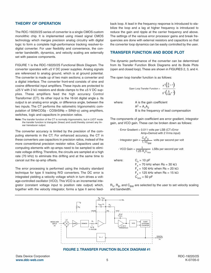
The open loop transfer function is as follows:
where: A is the gain coefficientA2 = A1A2B is the frequency of lead compensation
The components of gain coefficient are error gradient, integratorgain, and VCO gain. These can be broken down as follows:
where: Cs = 10 pFFs = 70 kHz when Rs = 30 kΩFs = 100 kHz when Rs = 20 kΩFs = 125 kHz when Rs = 15 kΩCvco = 50 pF
RV, RB, and CBW are selected by the user to set velocity scalingand bandwidth.
- Error Gradient = 0.011 volts per LSB (CT+Error Amp+Demod with 2 Vrms input)
- Integrator gain = volts per second per volt
- VCO Gain = LSBs per second per volt 11.25 RvCvco
CSFS
1.1CBW
Open Loop Transfer Function = A (S
B+ 1)2
S ( S10B
+ 1)2
GAIN
11 mV/LSB
16 BITUP/DOWNCOUNTER
R 1 VCO
R V
R B C BW
C /10 BW
VEL
-VCO
H = 1
-VSUM VEL
C F S S
CT
+
-
RESOLVERINPUT
(θ)
R S
50 pfC VCO
DIGITALOUTPUT
(φ)
DEMOD
±1.25 VTHRESHOLD
1
FIGURE 2.TRANSFER FUNCTION BLOCK DIAGRAM #1
back loop. A lead in the frequency response is introduced to sta-bilize the loop and a lag at higher frequency is introduced toreduce the gain and ripple at the carrier frequency and above.The settings of the various error processor gains and break fre-quencies are done with external resistors and capacitors so thatthe converter loop dynamics can be easily controlled by the user.
6Data Device Corporationwww.ddc-web.com
RDC-19220/2SK-07/05-0
4) The BIT output, which is active low, is activated by an error ofapproximately 100 LSBs. During normal operation, for stepinputs or on power up, a large error can exist.
5) Setup of bandwidth and velocity scaling for the optimized crit-ically damped case should proceed as follows:
As an example:
Calculate component values for a 16-bit converter with 100Hzbandwidth, a tracking rate of 10 RPS and a full scale velocityof 4 Volts.
Note: DDC has software available to perform the previous calculations. ContactDDC to request software or visit our web site at www.ddc-web.com todownload software.
6) Selecting a fBW that is too low relative to the maximum appli-cation tracking rate can create a spin-around condition inwhich the converter never settles. The relationship to insureagainst spin-around is as follows (TABLE 2.):
- Rv = = 97655 Ω
- Compute CBW (pF) = = 21955 pF
- Compute RB = = 410 kΩ
4 V10 rps x 216 x 50 pF x 1.25 V
0.921955 x 10 -12 x 100 Hz
3.2 x 67 kHz x 108
97655 x 100 Hz2
- Select the desired f BW (closed loop) based on overall system dynamics.
- Select f carrier ≥ 3.5f BW
- Select the applications tracking rate (in accordance with TABLE 3) and use appropriate values for R SET and R CLK
- Compute Rv =
- Compute CBW (pF) =
- Where Fs = 67 kHz for R CLK = 30 kΩ 100 kHz for R CLK = 20 kΩ 125 kHz for R CLK = 15 kΩ
- Compute RB =
- Compute
3.2 x Fs (Hz) x 108
Rv x (f BW)2
Full Scale Velocity VoltageTracking Rate (rps) x 2 resolution x 50 pF x 1.25 V
0.9CBW x f BW
CBW 10
TABLE 2. TRACKING/BW RELATIONSHIPRPS (MAX)/BW RESOLUTION
1 10
0.50 12
0.25 14
0.125 16
ERROR PROCESSOR
RESOLVERINPUT
(θ)
VELOCITYOUT
DIGITALPOSITIONOUT (φ)
VCOCT SA + 1 1 B
S S + 1 10B
H = 1
+
-
e A 2 S
-12 db/oct
B A
2A
-6 db/oct
10Bω (rad/sec)
2A 2 2 A ω (rad/sec)
f = BW (Hz) = BW 2 Aπ
CLOSED LOOP
(B = A/2)
GAIN = 0.4
GAIN = 4(CRITICALLY DAMPED)
OPEN LOOP
FIGURE 3.TRANSFER FUNCTION BLOCK DIAGRAM #2
FIGURE 4. BODE PLOTS
GENERAL SETUP CONDITIONSNote: For detailed application and technical information see the RD/RDC
Converter Applications Manual which is available for download from theDDC web site @www.ddc-web.com.
DDC has external component selection software which consid-ers all the criteria below and, in a simple fashion, asks the keyparameters (carrier frequency, resolution, bandwidth, and track-ing rate) to derive the external component values.
The following recommendations should be considered wheninstalling the RDC-19220/2S Resolver-to-Digital (R/D) converter:
1) When setting the bandwidth (BW) and Tracking Rate (TR)(selecting five external components), the system require-ments need to be considered. For the greatest noise immuni-ty, select the minimum BW and TR the system will allow.
2) Power supplies are ±5V DC. For lowest noise performance itis recommended that a 0.1µF or larger cap be connected fromeach supply to ground near the converter package. Whenusing +5V and -5V supplies to power the converter, pins 22,23, 25 and 26 must be no connection.
3) There are two internal ground planes to reduce analog inputnoise due to digital ground currents. The resolver inputs andvelocity output are referenced to AGND. The digital inputs andoutputs are referenced to GND. The AGND and GND pinsmust be tied together as close to the package as possible, orunstable results may occur.
7Data Device Corporationwww.ddc-web.com
RDC-19220/2SK-07/05-0
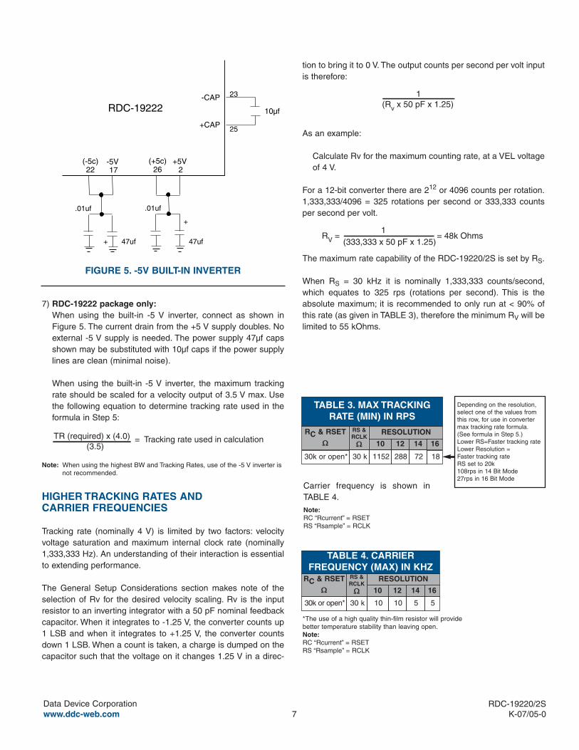
7) RDC-19222 package only:When using the built-in -5 V inverter, connect as shown inFigure 5. The current drain from the +5 V supply doubles. Noexternal -5 V supply is needed. The power supply 47µf capsshown may be substituted with 10µf caps if the power supplylines are clean (minimal noise).
When using the built-in -5 V inverter, the maximum trackingrate should be scaled for a velocity output of 3.5 V max. Usethe following equation to determine tracking rate used in theformula in Step 5:
Note: When using the highest BW and Tracking Rates, use of the -5 V inverter isnot recommended.
HIGHER TRACKING RATES AND CARRIER FREQUENCIES
Tracking rate (nominally 4 V) is limited by two factors: velocityvoltage saturation and maximum internal clock rate (nominally1,333,333 Hz). An understanding of their interaction is essentialto extending performance.
The General Setup Considerations section makes note of theselection of Rv for the desired velocity scaling. Rv is the inputresistor to an inverting integrator with a 50 pF nominal feedbackcapacitor. When it integrates to -1.25 V, the converter counts up1 LSB and when it integrates to +1.25 V, the converter countsdown 1 LSB. When a count is taken, a charge is dumped on thecapacitor such that the voltage on it changes 1.25 V in a direc-
TR (required) x (4.0) = Tracking rate used in calculation (3.5)
FIGURE 5. -5V BUILT-IN INVERTER
RDC-19222 10µf
23
25+CAP
-CAP
.01uf
(-5c) -5V22 17
.01uf
(+5c) +5V26 2
47uf 47uf
+
+
tion to bring it to 0 V. The output counts per second per volt inputis therefore:
As an example:
Calculate Rv for the maximum counting rate, at a VEL voltageof 4 V.
For a 12-bit converter there are 212 or 4096 counts per rotation.1,333,333/4096 = 325 rotations per second or 333,333 countsper second per volt.
The maximum rate capability of the RDC-19220/2S is set by RS.
When RS = 30 kHz it is nominally 1,333,333 counts/second,which equates to 325 rps (rotations per second). This is theabsolute maximum; it is recommended to only run at < 90% ofthis rate (as given in TABLE 3), therefore the minimum RV will belimited to 55 kOhms.
1 RV = = 48k Ohms
(333,333 x 50 pF x 1.25)
1 (Rv x 50 pF x 1.25)
RC & RSET
ΩΩ
TABLE 3. MAX TRACKINGRATE (MIN) IN RPS
RESOLUTION
10 12 14 16
30k or open* 30 k 1152 288 72 18
Depending on the resolution,select one of the values fromthis row, for use in convertermax tracking rate formula.(See formula in Step 5.)Lower RS=Faster tracking rateLower Resolution = Faster tracking rateRS set to 20k108rps in 14 Bit Mode27rps in 16 Bit Mode
Carrier frequency is shown in TABLE 4.Note:RC “Rcurrent” = RSETRS “Rsample” = RCLK
RS &RCLK
ΩΩ
*The use of a high quality thin-film resistor will providebetter temperature stability than leaving open.Note:RC “Rcurrent” = RSETRS “Rsample” = RCLK
55101030 k30k or open*
16141210
RESOLUTIONRS &RCLK
ΩΩ
RC & RSET
ΩΩ
TABLE 4. CARRIERFREQUENCY (MAX) IN KHZ
8Data Device Corporationwww.ddc-web.com
RDC-19220/2SK-07/05-0
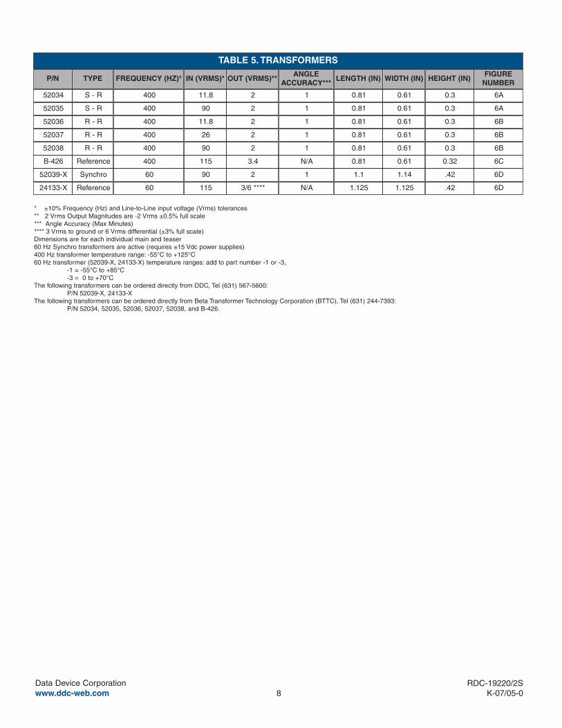
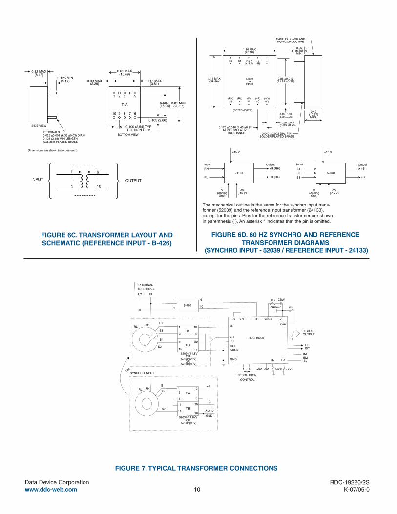
* ±10% Frequency (Hz) and Line-to-Line input voltage (Vrms) tolerances** 2 Vrms Output Magnitudes are -2 Vrms ±0.5% full scale*** Angle Accuracy (Max Minutes)**** 3 Vrms to ground or 6 Vrms differential (±3% full scale)Dimensions are for each individual main and teaser60 Hz Synchro transformers are active (requires ±15 Vdc power supplies)400 Hz transformer temperature range: -55°C to +125°C60 Hz transformer (52039-X, 24133-X) temperature ranges: add to part number -1 or -3,
-1 = -55°C to +85°C-3 = 0 to +70°C
The following transformers can be ordered directly from DDC, Tel (631) 567-5600:P/N 52039-X, 24133-X
The following transformers can be ordered directly from Beta Transformer Technology Corporation (BTTC), Tel (631) 244-7393:P/N 52034, 52035, 52036, 52037, 52038, and B-426.
3/6 ****11560Reference24133-X
29060Synchro52039-X
3.4115400ReferenceB-426
290400R - R52038
226400R - R52037
211.8400R - R52036
290400S - R52035
211.8400S - R52034
OUT (VRMS)**IN (VRMS)*FREQUENCY (HZ)*TYPEP/N
TABLE 5. TRANSFORMERS
1.125N/A
1.11
0.81N/A
0.811
0.811
0.811
0.811
0.811
LENGTH (IN)ANGLE
ACCURACY***
1.125
1.14
0.61
0.61
0.61
0.61
0.61
0.61
WIDTH (IN)
.42
.42
0.32
0.3
0.3
0.3
0.3
0.3
HEIGHT (IN)
6D
6D
6C
6B
6B
6B
6A
6A
FIGURENUMBER
9Data Device Corporationwww.ddc-web.com
RDC-19220/2SK-07/05-0
BOTTOM VIEW
0.81 MAX(20.57)
0.30 MAX(7.62)
0.61 MAX(15.49)
0.15 MAX(3.81)
0.09 MAX(2.29)
0.100 (2.54) TYPTOL NON CUM
0.61 MAX(15.49)
0.15 MAX(3.81)
0.09 MAX(2.29)
0.600(15.24)
0.115 MAX(2.92)
1 3 4 5
10 9 8 7 6
11 12 14 15
20 19 18 17 16
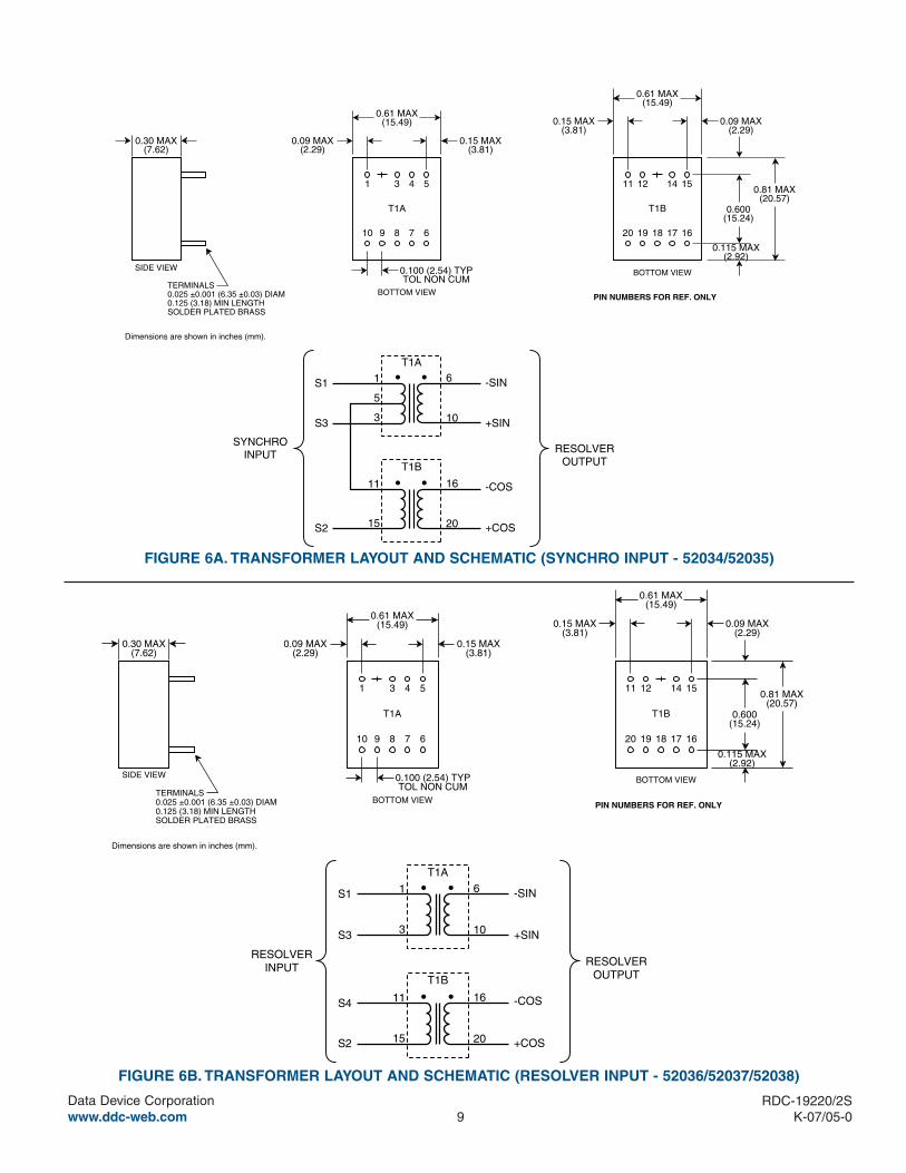
PIN NUMBERS FOR REF. ONLYTERMINALS0.025 ±0.001 (6.35 ±0.03) DIAM0.125 (3.18) MIN LENGTHSOLDER PLATED BRASS
T1A T1B
BOTTOM VIEWSIDE VIEW
Dimensions are shown in inches (mm).
1
5
3
6
10
11
15
16
20
T1A
T1B
SYNCHROINPUT RESOLVER
OUTPUT
-SIN
+SIN
-COS
+COS
S1
S3
S2
FIGURE 6A. TRANSFORMER LAYOUT AND SCHEMATIC (SYNCHRO INPUT - 52034/52035)
FIGURE 6B. TRANSFORMER LAYOUT AND SCHEMATIC (RESOLVER INPUT - 52036/52037/52038)
1
3
6
10
11
15
16
20
T1A
T1B
RESOLVERINPUT RESOLVER
OUTPUT
-SIN
+SIN
-COS
+COS
S1
S3
S2
S4
BOTTOM VIEW
0.81 MAX(20.57)
0.30 MAX(7.62)
0.61 MAX(15.49)
0.15 MAX(3.81)
0.09 MAX(2.29)
0.100 (2.54) TYPTOL NON CUM
0.61 MAX(15.49)
0.15 MAX(3.81)
0.09 MAX(2.29)
0.600(15.24)
0.115 MAX(2.92)
1 3 4 5
10 9 8 7 6
11 12 14 15
20 19 18 17 16
PIN NUMBERS FOR REF. ONLYTERMINALS0.025 ±0.001 (6.35 ±0.03) DIAM0.125 (3.18) MIN LENGTHSOLDER PLATED BRASS
T1A T1B
BOTTOM VIEWSIDE VIEW
Dimensions are shown in inches (mm).
10Data Device Corporationwww.ddc-web.com
RDC-19220/2SK-07/05-0
1
5
6
10
INPUT OUTPUT
BOTTOM VIEW
0.32 MAX(8.13)
0.61 MAX(15.49)
0.15 MAX(3.81)
0.09 MAX(2.29)
0.100 (2.54) TYPTOL NON CUM
1 32 5
10 9 8 7 6
TERMINALS0.025 ±0.001 (6.35 ±0.03) DIAM0.125 (3.18) MIN LENGTHSOLDER-PLATED BRASS
T1A
SIDE VIEW
Dimensions are shown in inches (mm).
0.105 (2.66)
0.600 (15.24)
0.81 MAX(20.57)
0.125 MIN(3.17)
FIGURE 6C. TRANSFORMER LAYOUT ANDSCHEMATIC (REFERENCE INPUT - B-426)
B-426
1
5
6
10
RLRH
RL RH
S1
S3
S4
S2
1
3 6
10
11
15
20
16
EXTERNAL
REFERENCE
LO HI
-S SIN -R +R -VSUM VEL
-VCO
DIGITALOUTPUT
16
CBBIT
INHEMEL
A B +5V -5V
+S
+C-C
COSAGND
GND
RDC-19220
TIB
TIA
TIA
TIB
S1
S3
S2
RESOLUTION
CONTROL
52036(11.8V)
52037(26V)OR
52038(90V)OR
52034(11.8V)
52037(90V)OR
1
310
6
16
11
15
20
5
ORSYNCHRO INPUT
+S
+C
AGND
GND
Rs Rc
RB CBW
CBW/10 RV
30K Ω 30K Ω
FIGURE 7. TYPICAL TRANSFORMER CONNECTIONS
1.14 MAX(28.96)
CASE IS BLACK ANDNON-CONDUCTIVE
1.14 MAX(28.96)
•
*S1•
*S3
•
(+15 V)+15 V
•
(-R)+S
+
**
(RH)
•S2
(RL)
+*
(V)
•V
(+R)
•+C
(-Vs)
•-Vs
52039or
24133
0.21 ±0.3(5.33 ±0.76)
0.85 ±0.010(21.59 ±0.25)
0.175 ±0.010 (4.45 ±0.25)NONCUMULATIVE
TOLERANCE 0.040 ±0.002 DIA. PIN.SOLDER PLATED BRASS
0.42(10.67)MAX.
0.25(6.35)MIN.
(BOTTOM VIEW)
0.13 ±0.03(3.30 ±0.76)
RH
RL
+15 V
V(Analog
Gnd)
-Vs(-15 V)
Output+R (RH)
-R (RL)24133
Input
S1
+15 V
V(Analog
Gnd)
-Vs(-15 V)
Output+S
+C52039
Input
S2
S3
The mechanical outline is the same for the synchro input trans-former (52039) and the reference input transformer (24133),except for the pins. Pins for the reference transformer are shownin parenthesis ( ). An asterisk * indicates that the pin is omitted.
FIGURE 6D. 60 HZ SYNCHRO AND REFERENCETRANSFORMER DIAGRAMS
(SYNCHRO INPUT - 52039 / REFERENCE INPUT - 24133)
11Data Device Corporationwww.ddc-web.com
RDC-19220/2SK-07/05-0
R 1
R 3
R 2
R 4
EXTERNALREF
LO HI
RESOLVER
S4
S3
S1
S2
GND
+S
-SSINCOS-C
+C
A GND
-R +R
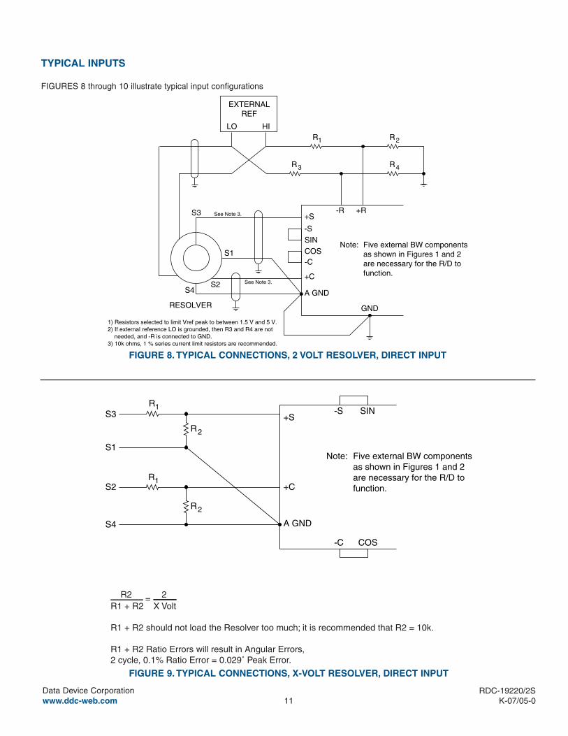
1) Resistors selected to limit Vref peak to between 1.5 V and 5 V.2) If external reference LO is grounded, then R3 and R4 are not needed, and -R is connected to GND.3) 10k ohms, 1 % series current limit resistors are recommended.
See Note 3.
See Note 3.
Note: Five external BW componentsas shown in Figures 1 and 2are necessary for the R/D tofunction.
R 1
R 2
S3
S1
S2
+S-S SIN
COS-C
+C
A GNDS4
R 1
R 2
R2 2 =R1 + R2 X Volt
R1 + R2 should not load the Resolver too much; it is recommended that R2 = 10k.
R1 + R2 Ratio Errors will result in Angular Errors,2 cycle, 0.1% Ratio Error = 0.029˚ Peak Error.
Note: Five external BW componentsas shown in Figures 1 and 2are necessary for the R/D tofunction.
FIGURE 8. TYPICAL CONNECTIONS, 2 VOLT RESOLVER, DIRECT INPUT
FIGURE 9. TYPICAL CONNECTIONS, X-VOLT RESOLVER, DIRECT INPUT
TYPICAL INPUTS
FIGURES 8 through 10 illustrate typical input configurations
12Data Device Corporationwww.ddc-web.com
RDC-19220/2SK-07/05-0
R iS1
S3+S
-S
SIN
R f
R i
R f
R iS4
S2+C
-C
R f
R i
R f
COSA GNDRESOLVER
INPUT
CONVERTER
-
+
-
+
Note: Five external BW componentsas shown in Figures 1 and 2are necessary for the R/D tofunction.
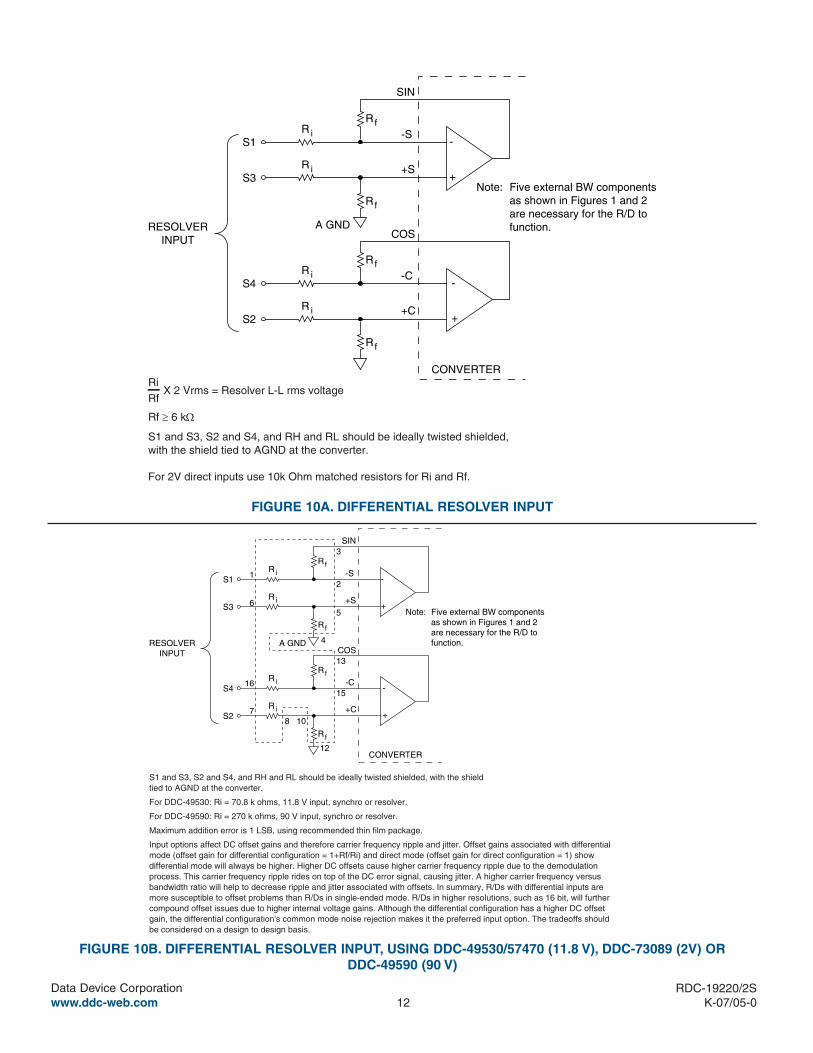
Ri X 2 Vrms = Resolver L-L rms voltageRf
Rf ≥ 6 kΩ
S1 and S3, S2 and S4, and RH and RL should be ideally twisted shielded,with the shield tied to AGND at the converter.
For 2V direct inputs use 10k Ohm matched resistors for Ri and Rf.
R iS1
S3+S
-S
SIN
R f
R i
R f
R iS4
S2+C
-C
R f
R i
R f
COSA GND
CONVERTER
8 10
12
15
13
2
3
1
6
16
7
4
5
-
+
-
+
RESOLVERINPUT
Note: Five external BW componentsas shown in Figures 1 and 2are necessary for the R/D tofunction.
S1 and S3, S2 and S4, and RH and RL should be ideally twisted shielded, with the shield tied to AGND at the converter.
For DDC-49530: Ri = 70.8 k ohms, 11.8 V input, synchro or resolver.
For DDC-49590: Ri = 270 k ohms, 90 V input, synchro or resolver.
Maximum addition error is 1 LSB, using recommended thin film package.
Input options affect DC offset gains and therefore carrier frequency ripple and jitter. Offset gains associated with differential mode (offset gain for differential configuration = 1+Rf/Ri) and direct mode (offset gain for direct configuration = 1) show differential mode will always be higher. Higher DC offsets cause higher carrier frequency ripple due to the demodulation process. This carrier frequency ripple rides on top of the DC error signal, causing jitter. A higher carrier frequency versus bandwidth ratio will help to decrease ripple and jitter associated with offsets. In summary, R/Ds with differential inputs are more susceptible to offset problems than R/Ds in single-ended mode. R/Ds in higher resolutions, such as 16 bit, will further compound offset issues due to higher internal voltage gains. Although the differential configuration has a higher DC offset gain, the differential configuration's common mode noise rejection makes it the preferred input option. The tradeoffs should be considered on a design to design basis.
FIGURE 10A. DIFFERENTIAL RESOLVER INPUT
FIGURE 10B. DIFFERENTIAL RESOLVER INPUT, USING DDC-49530/57470 (11.8 V), DDC-73089 (2V) OR DDC-49590 (90 V)
13Data Device Corporationwww.ddc-web.com
RDC-19220/2SK-07/05-0
R iS1
S3+S
-S
SIN
R f
R i
R f
R i
S2+C
-C
R /2 i
COS
A GND
CONVERTER
R i
R / 3 f
R / 3 f
-
+
-
+
Ri X 2 Vrms = Resolver L-L rms voltageRf
Rf ≥ 6 kΩ
S1, S2, and S3 should be triple twisted shielded; RH and RL should be twisted shielded, In both cases the shield should be tied to AGND at the converter.
Note: Five external BW componentsas shown in Figures 1 and 2are necessary for the R/D tofunction.
R iS1
S3+S
-S
SIN
R f
R i
R f
R i
S2+C
-C
R /2 i
COS
A GND
CONVERTER
815
11
15
14
2
3
1
6
16
7
4
5
R i
9
R / 3 f
R / 3 f
10
-
+
-
+
Note: Five external BW componentsas shown in Figures 1 and 2are necessary for the R/D tofunction.
S1, S2, and S3 should be triple twisted shielded; RH and RL should be twisted shielded, In both cases the shield should be tied to AGND at the converter.90 V input = DDC-49590: Ri = 270 kΩ, 90 V input, synchro or resolver.11.8 V input = DDC-49530: Ri = 70.8 kΩ, 11.8 V input, synchro or resolver.Maximum addition error is 1 LSB.
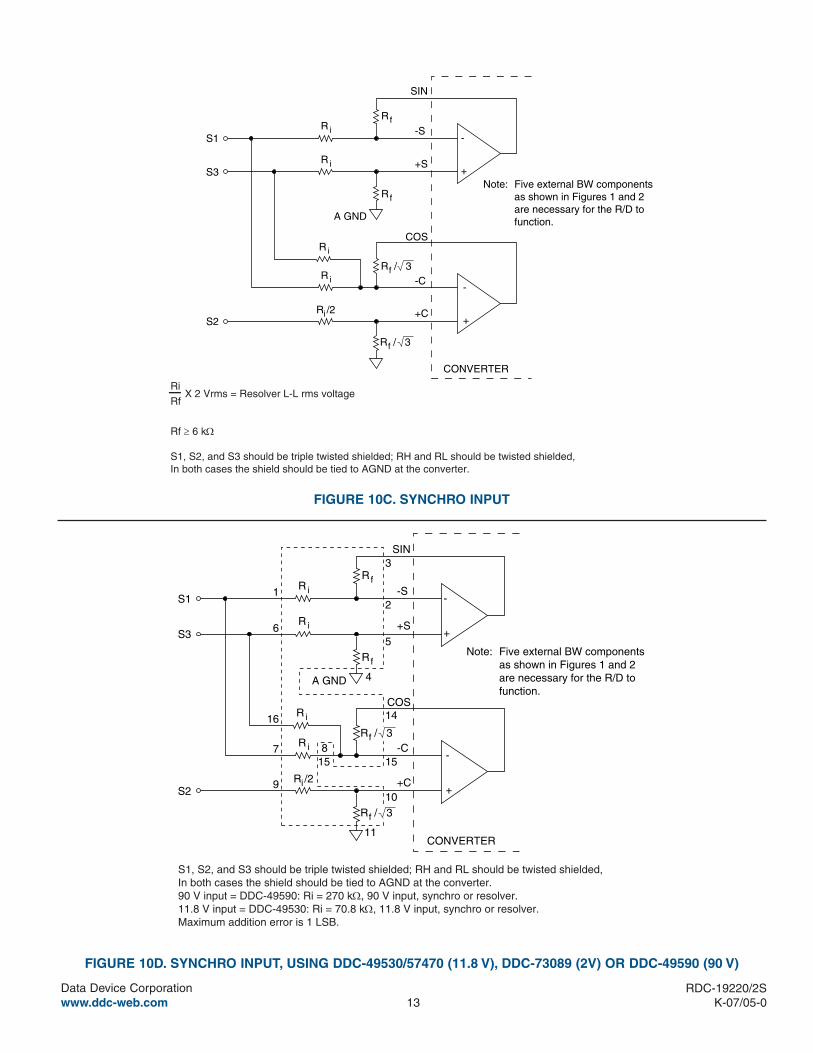
FIGURE 10C. SYNCHRO INPUT
FIGURE 10D. SYNCHRO INPUT, USING DDC-49530/57470 (11.8 V), DDC-73089 (2V) OR DDC-49590 (90 V)
14Data Device Corporationwww.ddc-web.com
RDC-19220/2SK-07/05-0
VELOCITY TRIMMING
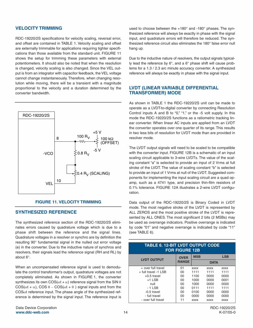
RDC-19220/2S specifications for velocity scaling, reversal error,and offset are contained in TABLE 1. Velocity scaling and offsetare externally trimmable for applications requiring tighter specifi-cations than those available from the standard unit. FIGURE 11shows the setup for trimming these parameters with externalpotentiometers. It should also be noted that when the resolutionis changed, velocity scaling is also changed. Since the VEL out-put is from an integrator with capacitor feedback, the VEL voltagecannot change instantaneously. Therefore, when changing reso-lution while moving, there will be a transient with a magnitudeproportional to the velocity and a duration determined by theconverter bandwidth.
8
10
-VCO
VEL
+5 V
-5 V
100 kΩ(OFFSET)
100 R V
0.8 R V
0.4 R (SCALING) V
RDC-19220/2S
FIGURE 11. VELOCITY TRIMMING
used to choose between the +180° and -180° phases. The syn-thesized reference will always be exactly in phase with the signalinput, and quadrature errors will therefore be reduced. The syn-thesized reference circuit also eliminates the 180° false error nullhang up.
Due to the inductive nature of resolvers, the output signals typical-ly lead the reference by 6°, and a 6° phase shift will cause prob-lems for a 1.3 / 2.3 arc minute accuracy converter. A synthesizedreference will always be exactly in phase with the signal input.
LVDT (LINEAR VARIABLE DIFFERENTIALTRANSFORMER) MODE
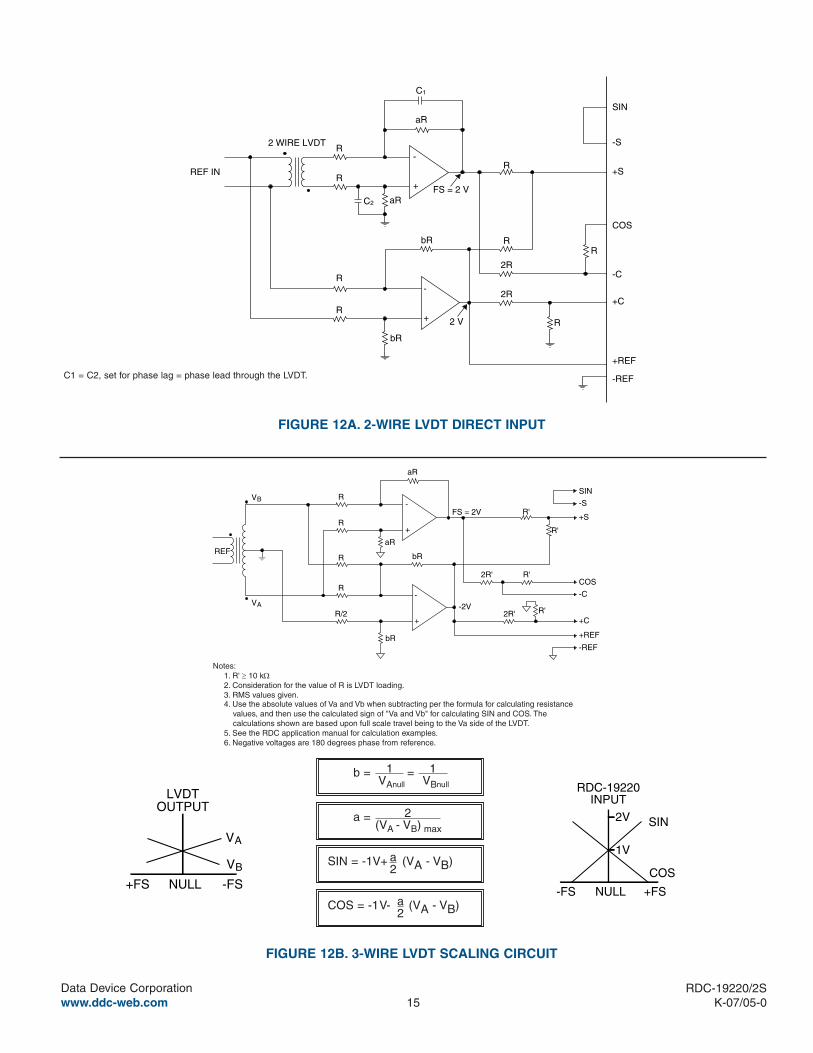
As shown in TABLE 1 the RDC-19220/2S unit can be made tooperate as a LVDT-to-digital converter by connecting ResolutionControl inputs A and B to “0,” “1,” or the -5 volt supply. In thismode the RDC-19220/2S functions as a ratiometric tracking lin-ear converter. When linear AC inputs are applied from an LVDTthe converter operates over one quarter of its range. This resultsin two less bits of resolution for LVDT mode than are provided inresolver mode.
The LVDT output signals will need to be scaled to be compatiblewith the converter input. FIGURE 12B is a schematic of an inputscaling circuit applicable to 3-wire LVDTs. The value of the scal-ing constant “a” is selected to provide an input of 2 Vrms at fullstroke of the LVDT. The value of scaling constant “b” is selectedto provide an input of 1 Vrms at null of the LVDT. Suggested com-ponents for implementing the input scaling circuit are a quad op-amp, such as a 4741 type, and precision thin-film resistors of0.1% tolerance. FIGURE 12A illustrates a 2-wire LVDT configu-ration.
Data output of the RDC-19220/2S is Binary Coded in LVDTmode. The most negative stroke of the LVDT is represented byALL ZEROS and the most positive stroke of the LVDT is repre-sented by ALL ONES. The most significant 2 bits (2 MSBs) maybe used as overrange indicators. Positive overrange is indicatedby code “01” and negative overrange is indicated by code “11”(see TABLE 6).
SYNTHESIZED REFERENCE
The synthesized reference section of the RDC-19220/2S elimi-nates errors caused by quadrature voltage which is due to aphase shift between the reference and the signal lines.Quadrature voltages in a resolver or synchro are by definition theresulting 90° fundamental signal in the nulled out error voltage(e) in the converter. Due to the inductive nature of synchros andresolvers, their signals lead the reference signal (RH and RL) byabout 6°.
When an uncompensated reference signal is used to demodu-late the control transformer’s output, quadrature voltages are notcompletely eliminated. As shown in FIGURE 1, the convertersynthesizes its own COS(ωt + α) reference signal from the SIN θCOS(ωt + α), COS θ − COS(ωt + θ ) signal inputs and from theCOSωt reference input. The phase angle of the synthesized ref-erence is determined by the signal input. The reference input is
TABLE 6. 12-BIT LVDT OUTPUT CODEFOR FIGURE 12B
DATA
+ over full travel+ full travel -1 LSB
+0.5 travel+1 LSB
null- 1 LSB
-0.5 travel- full travel
- over full travel
01 xxxx xxxx xxxx00 1111 1111 111100 1100 0000 000000 1000 0000 000100 1000 0000 000000 0111 1111 111100 0100 0000 000000 0000 0000 000011 xxxx xxxx xxxx
LVDT OUTPUTMSB LSBOVER
RANGE
15Data Device Corporationwww.ddc-web.com
RDC-19220/2SK-07/05-0
+S
-S
SIN
aR
R
+C
-C
COS
R'
-
+
-
+R/2
R
R
aR
bR
2R'
2R'
R'
bR +REF
-REF
R'
R'
R
V B
V A
Notes: 1. R' ≥ 10 kΩ 2. Consideration for the value of R is LVDT loading.
3. RMS values given.
FS = 2V
-2V
4. Use the absolute values of Va and Vb when subtracting per the formula for calculating resistance values, and then use the calculated sign of "Va and Vb" for calculating SIN and COS. The calculations shown are based upon full scale travel being to the Va side of the LVDT. 5. See the RDC application manual for calculation examples.
6. Negative voltages are 180 degrees phase from reference.
REF
V B
V A
LVDTOUTPUT
+FS -FSNULLCOS
SIN
RDC-19220INPUT
-FS +FSNULL
1V
2V
1 1 b = = VAnull VBnull
2 a = (VA - VB) max
aSIN = -1V+ (VA - VB) 2
aCOS = -1V- (VA - VB) 2
FIGURE 12B. 3-WIRE LVDT SCALING CIRCUIT
+S
-S
SIN
aR
R
+C
-C
COS
R
-
+
-
+R
R
R
aR
C 1
bR
2R
2R
R
bR
+REF
-REF
R
C 2
2 WIRE LVDT
REF IN
R
2 V
FS = 2 V
FIGURE 12A. 2-WIRE LVDT DIRECT INPUT
C1 = C2, set for phase lag = phase lead through the LVDT.
16Data Device Corporationwww.ddc-web.com
RDC-19220/2SK-07/05-0
INHIBIT, ENABLE, AND CB TIMING
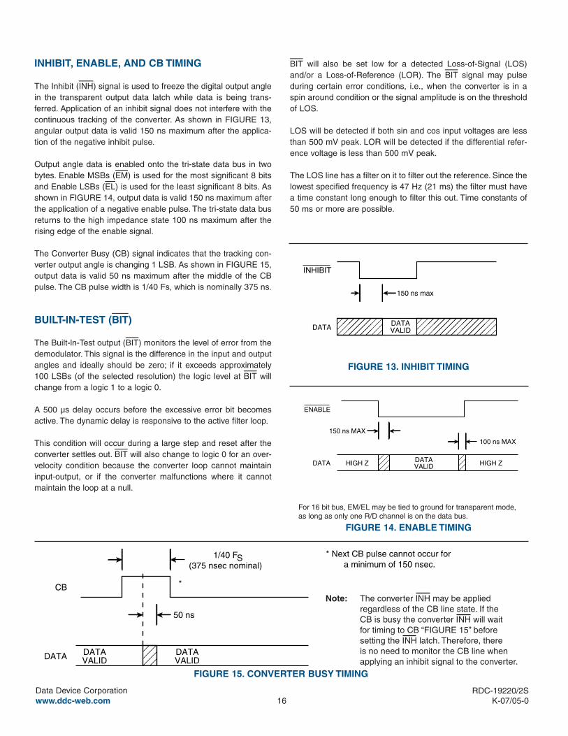
The Inhibit (INH) signal is used to freeze the digital output anglein the transparent output data latch while data is being trans-ferred. Application of an inhibit signal does not interfere with thecontinuous tracking of the converter. As shown in FIGURE 13,angular output data is valid 150 ns maximum after the applica-tion of the negative inhibit pulse.
Output angle data is enabled onto the tri-state data bus in twobytes. Enable MSBs (EM) is used for the most significant 8 bitsand Enable LSBs (EL) is used for the least significant 8 bits. Asshown in FIGURE 14, output data is valid 150 ns maximum afterthe application of a negative enable pulse. The tri-state data busreturns to the high impedance state 100 ns maximum after therising edge of the enable signal.
The Converter Busy (CB) signal indicates that the tracking con-verter output angle is changing 1 LSB. As shown in FIGURE 15,output data is valid 50 ns maximum after the middle of the CBpulse. The CB pulse width is 1/40 Fs, which is nominally 375 ns.
BUILT-IN-TEST (BIT)
The Built-ln-Test output (BIT) monitors the level of error from thedemodulator. This signal is the difference in the input and outputangles and ideally should be zero; if it exceeds approximately100 LSBs (of the selected resolution) the logic level at BIT willchange from a logic 1 to a logic 0.
A 500 µs delay occurs before the excessive error bit becomesactive. The dynamic delay is responsive to the active filter loop.
This condition will occur during a large step and reset after theconverter settles out. BIT will also change to logic 0 for an over-velocity condition because the converter loop cannot maintaininput-output, or if the converter malfunctions where it cannotmaintain the loop at a null.
BIT will also be set low for a detected Loss-of-Signal (LOS)and/or a Loss-of-Reference (LOR). The BIT signal may pulseduring certain error conditions, i.e., when the converter is in aspin around condition or the signal amplitude is on the thresholdof LOS.
LOS will be detected if both sin and cos input voltages are lessthan 500 mV peak. LOR will be detected if the differential refer-ence voltage is less than 500 mV peak.
The LOS line has a filter on it to filter out the reference. Since thelowest specified frequency is 47 Hz (21 ms) the filter must havea time constant long enough to filter this out. Time constants of50 ms or more are possible.
DATADATAVALID
150 ns max
INHIBIT
100 ns MAX
ENABLE
150 ns MAX
DATA DATAVALIDHIGH Z HIGH Z
For 16 bit bus, EM/EL may be tied to ground for transparent mode, as long as only one R/D channel is on the data bus.
1/40 F S(375 nsec nominal)
CB
50 ns
DATA DATAVALID
DATAVALID
*
* Next CB pulse cannot occur for a minimum of 150 nsec.
Note: The converter INH may be applied regardless of the CB line state. If the CB is busy the converter INH will wait for timing to CB “FIGURE 15” before setting the INH latch. Therefore, there is no need to monitor the CB line when applying an inhibit signal to the converter.
FIGURE 13. INHIBIT TIMING
FIGURE 14. ENABLE TIMING
FIGURE 15. CONVERTER BUSY TIMING
17Data Device Corporationwww.ddc-web.com
RDC-19220/2SK-07/05-0
Built-In-TestBIT21GroundGND20
Converter BusyCB22Analog GroundA GND19
MSBBit 123Enable MSBsEM18
Bit 924Current SetRC17
Bit 225Sampling SetRS16
Bit 1026Power Supply-5 V15
Bit 327Signal Input-S14
Bit 1128Signal Input+SIN13
Bit 429Signal Input+S12
Bit 1230Signal Input-C11
Bit 531Signal InputCOS10
Bit 1332Signal Input+C9
Bit 633Velocity OutputVEL8
Bit 1434Vel Sum Point-VSUM7
Bit 735Neg. VCO Input-VCO6
Bit 1536-Reference Input-REF5
Bit 837+Reference Input+REF4
LSBBit 1638InhibitINH3
Enable LSBsEL39Resolution ControlB2
Power Supply+5 V40Resolution ControlA1
DESCRIPTIONNAME#DESCRIPTIONNAME#
PIN OUT FUNCTION TABLES BY MODEL NUMBER
The following tables detail pin out functions by the DDC modelnumber.
Neg.Terminal
Ground
Pos. Terminal
Neg. Supply Cap
Analog Ground
Enable MSBs
Pos. Supply CapCurrent Set
Built-in-TestSampling Set
Converter BusyPower Supply
MSBSignal Input
Signal Input
Signal Input
Signal Input
Signal Input
Signal Input
Velocity Output
Vel Sum Point
Neg. VCO Input
-Reference Input
+Reference Input
Inhibit
Resolution Control
Resolution Control
Power Supply (see note)
LSBEnable LSBs
DESCRIPTION
-CAP
GND
+CAP
23
24
25
-5C (-5V)
A GND
EM
22
21
20
+5C(+5V)26RC19
BIT27RS18
CB28-5V17
Bit 129-S16
Bit 930SIN15
Bit 231+S14
Bit 1032-C13
Bit 333COS12
Bit 1134+C11
Bit 435VEL10
Bit 1236-VSUM9
Bit 537-VCO8
Bit 1338-REF7
Bit 639+REF6
Bit 1440INH5
Bit 741B4
Bit 1542A3
BIT 843+5V2
BIT 1644EL1
NAME#NAME# DESCRIPTION
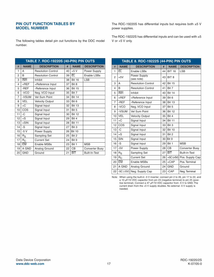
TABLE 8. RDC-19222S (44-PIN) PIN OUTSTABLE 7. RDC-19220S (40-PIN) PIN OUTS
Note: When using the built-in -5 V inverter: connect pin 2 to 26, pin 17 to 22, anda 10 µF/10 VDC capacitor from pin 23 (negative terminal) to pin 25 (posi-tive terminal). Connect a 47 µF/10 VDC capacitor from -5 V to GND. Thecurrent drain from the +5 V supply doubles. No external -5 V supply isneeded.
The RDC-19220S has differential inputs but requires both ±5 Vpower supplies.
The RDC-19222S has differential inputs and can be used with ±5V or +5 V only.
18Data Device Corporationwww.ddc-web.com
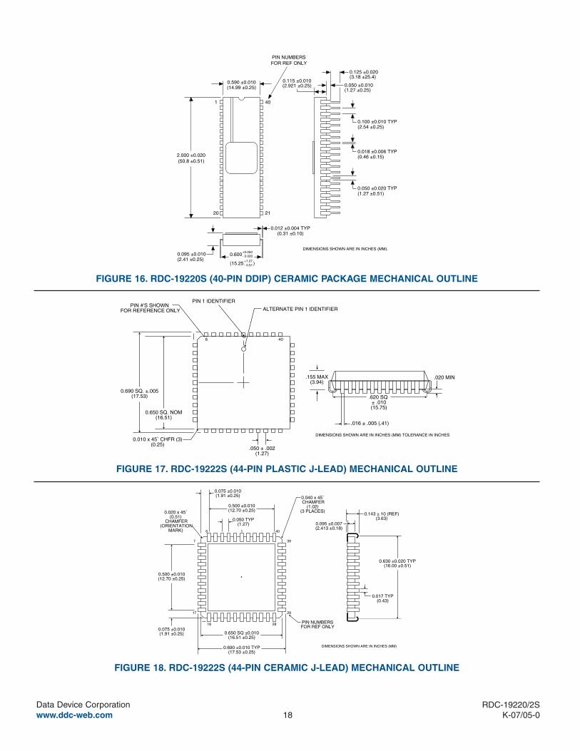
RDC-19220/2SK-07/05-0
2.000 ±0.020(50.8 ±0.51)
0.590 ±0.010(14.99 ±0.25)
0.100 ±0.010 TYP(2.54 ±0.25)
0.018 ±0.006 TYP(0.46 ±0.15)
0.050 ±0.020 TYP(1.27 ±0.51)
0.012 ±0.004 TYP(0.31 ±0.10)
+0.0500.600 - 0.020
+1.27 (15.25 ) - 0.51
DIMENSIONS SHOWN ARE IN INCHES (MM).
1
20
0.125 ±0.020(3.18 ±25.4)
0.050 ±0.010(1.27 ±0.25)
0.115 ±0.010(2.921 ±0.25)
40
21
PIN NUMBERSFOR REF ONLY
0.095 ±0.010(2.41 ±0.25)
FIGURE 16. RDC-19220S (40-PIN DDIP) CERAMIC PACKAGE MECHANICAL OUTLINE
ALTERNATE PIN 1 IDENTIFIER
0.650 SQ. NOM(16.51)
0.690 SQ. ±.005(17.53)
DIMENSIONS SHOWN ARE IN INCHES (MM) TOLERANCE IN INCHES
PIN 1 IDENTIFIER
.050 ± .002(1.27)
0.010 x 45˚ CHFR (3)(0.25)
6 40
.020 MIN
.620 SQ ± .010(15.75)
.016 ± .005 (.41)
.155 MAX(3.94)
PIN #'S SHOWN FOR REFERENCE ONLY
FIGURE 17. RDC-19222S (44-PIN PLASTIC J-LEAD) MECHANICAL OUTLINE
0.630 ±0.020 TYP(16.00 ±0.51)
0.500 ±0.010(12.70 ±0.25)
DIMENSIONS SHOWN ARE IN INCHES (MM)
0.020 x 45˚(0.51)
CHAMFER (ORIENTATION
MARK)
0.040 x 45˚ CHAMFER
(1.02)(3 PLACES)
0.143 ± 10 (REF)(3.63)
0.095 ±0.007(2.413 ±0.18)
6 40
0.075 ±0.010(1.91 ±0.25)
17
18 28
29
39
1
0.075 ±0.010(1.91 ±0.25)
0.500 ±0.010(12.70 ±0.25)
0.050 TYP(1.27)
7
0.650 SQ ±0.010(16.51 ±0.25)
0.690 ±0.010 TYP(17.53 ±0.25)
PIN NUMBERSFOR REF ONLY
0.017 TYP(0.43)
FIGURE 18. RDC-19222S (44-PIN CERAMIC J-LEAD) MECHANICAL OUTLINE
19Data Device Corporationwww.ddc-web.com
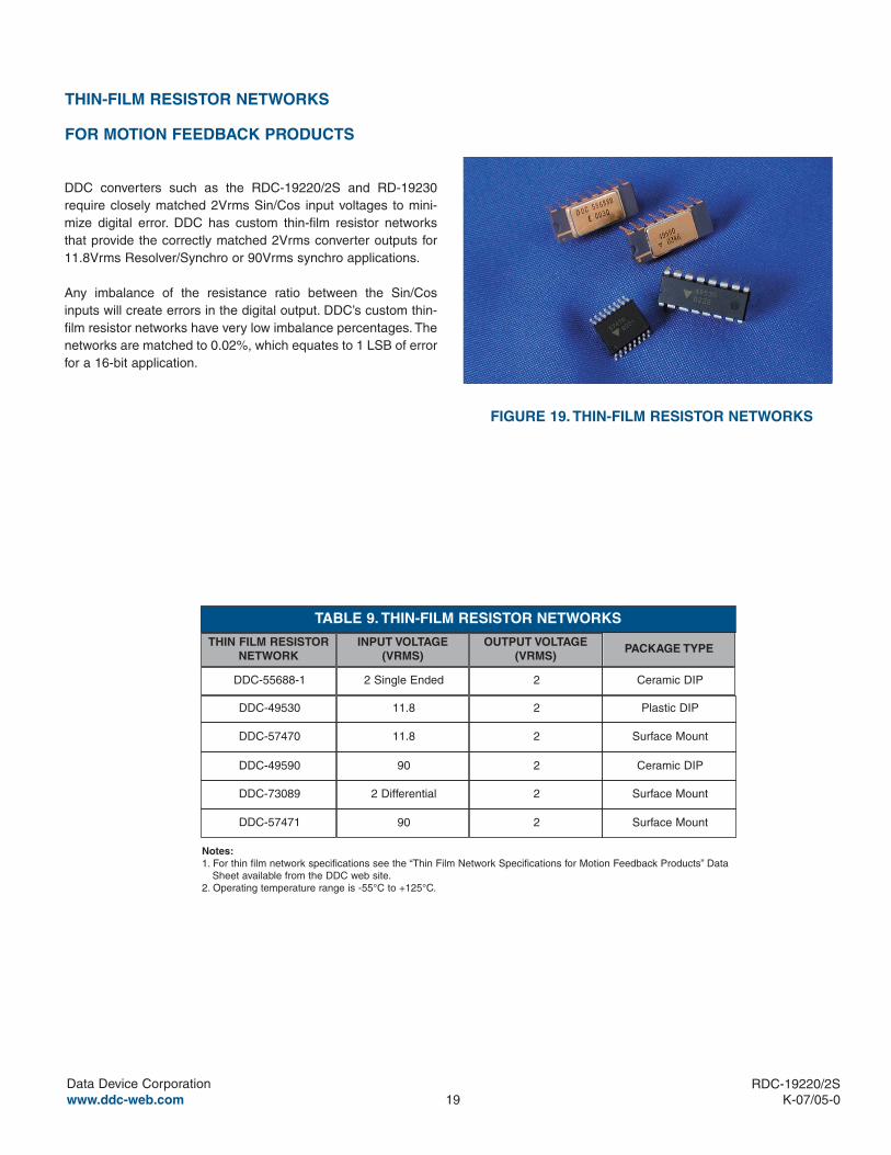
RDC-19220/2SK-07/05-0
THIN FILM RESISTORNETWORK
DDC-55688-1
INPUT VOLTAGE(VRMS)
OUTPUT VOLTAGE(VRMS)
PACKAGE TYPE
2 Single Ended 2 Ceramic DIP
DDC-49530 11.8 2 Plastic DIP
DDC-57470 11.8 2 Surface Mount
DDC-49590 90 2 Ceramic DIP
DDC-73089 2 Differential 2 Surface Mount
DDC-57471 90 2 Surface Mount
DDC converters such as the RDC-19220/2S and RD-19230require closely matched 2Vrms Sin/Cos input voltages to mini-mize digital error. DDC has custom thin-film resistor networksthat provide the correctly matched 2Vrms converter outputs for11.8Vrms Resolver/Synchro or 90Vrms synchro applications.
Any imbalance of the resistance ratio between the Sin/Cosinputs will create errors in the digital output. DDC’s custom thin-film resistor networks have very low imbalance percentages. Thenetworks are matched to 0.02%, which equates to 1 LSB of errorfor a 16-bit application.
THIN-FILM RESISTOR NETWORKS
FOR MOTION FEEDBACK PRODUCTS
Notes:1. For thin film network specifications see the “Thin Film Network Specifications for Motion Feedback Products” Data
Sheet available from the DDC web site.2. Operating temperature range is -55°C to +125°C.
FIGURE 19. THIN-FILM RESISTOR NETWORKS
TABLE 9. THIN-FILM RESISTOR NETWORKS
ORDERING INFORMATIONRDC-19222S -XXXX (Plastic Package: 44-pin J-Lead)
Supplemental Process Requirements:T = Tape and ReelBlank = None of the Above
Accuracy:2 = 4 minutes + 1 LSB3 = 2 minutes + 1 LSB5 = 1 minute + 1 LSB (maximum reference frequency = 5kHz)
Process Requirements:0 = No Burn-In9 = Solder Dip, without Burn-In
Temperature Grade:2 = -40 to +85°C3 = 0 to +70°C
Package Options:S = StandardSG = Lead Free
20Data Device Corporationwww.ddc-web.com
RDC-19220/2SK-07/05-0
—DDC ATPELECTRICAL TEST
—2017INSPECTION / WORKMANSHIP
CONDITION(S)METHOD(S)
MIL-STD-883TEST
STANDARD DDC PROCESSINGFOR PLASTIC MONOLITHIC PRODUCTS
21Data Device Corporationwww.ddc-web.com
RDC-19220/2SK-07/05-0
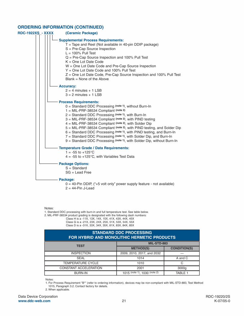
ORDERING INFORMATION (CONTINUED)RDC-1922XS - XXXX (Ceramic Package)
Supplemental Process Requirements:T = Tape and Reel (Not available in 40-pin DDIP package)S = Pre-Cap Source InspectionL = 100% Pull TestQ = Pre-Cap Source Inspection and 100% Pull TestK = One Lot Date CodeW = One Lot Date Code and Pre-Cap Source InspectionY = One Lot Date Code and 100% Pull TestZ = One Lot Date Code, Pre-Cap Source Inspection and 100% Pull TestBlank = None of the Above
Accuracy:2 = 4 minutes + 1 LSB3 = 2 minutes + 1 LSB
Process Requirements:0 = Standard DDC Processing (note 1), without Burn-In1 = MIL-PRF-38534 Compliant (note 2)
2 = Standard DDC Processing (note 1), with Burn-In3 = MIL-PRF-38534 Compliant (note 2), with PIND testing4 = MIL-PRF-38534 Compliant (note 2), with Solder Dip5 = MIL-PRF-38534 Compliant (note 2), with PIND testing, and Solder Dip6 = Standard DDC Processing (note 1), with PIND testing, and Burn-In7 = Standard DDC Processing (note 1), with Solder Dip, and Burn-In9 = Standard DDC Processing (note 1), with Solder Dip, without Burn-In
Temperature Grade / Data Requirements:1 = -55 to +125°C4 = -55 to +125°C, with Variables Test Data
Package Options:S = StandardSG = Lead Free
Package:0 = 40-Pin DDIP, (“+5 volt only” power supply feature - not available)2 = 44-Pin J-Lead
TABLE 11015 (note 1), 1030 (note 2)BURN-IN
Notes:1. For Process Requirement "B*" (refer to ordering information), devices may be non-compliant with MIL-STD-883, Test Method
1015, Paragraph 3.2. Contact factory for details.2. When applicable.
3000g2001CONSTANT ACCELERATION
C1010TEMPERATURE CYCLE
A and C1014SEAL
—2009, 2010, 2017, and 2032INSPECTION
CONDITION(S)METHOD(S)
MIL-STD-883TEST
STANDARD DDC PROCESSINGFOR HYBRID AND MONOLITHIC HERMETIC PRODUCTS
Notes:1. Standard DDC processing with burn-in and full temperature test. See table below.2. MIL-PRF-38534 product grading is designated with the following dash numbers:
Class H is a -11X, 13X, 14X, 15X, 41X, 43X, 44X, 45XClass G is a -21X, 23X, 24X, 25X, 51X, 53X, 54X, 55XClass D is a -31X, 33X, 34X, 35X, 81X, 83X, 84X, 85X
DATA DEVICE CORPORATIONREGISTERED TO ISO 9001:2000
FILE NO. A5976
RE
G ISTERED FIRM
®U
22K-07/05-0 PRINTED IN THE U.S.A.
105 Wilbur Place, Bohemia, New York, U.S.A. 11716-2482
For Technical Support - 1-800-DDC-5757 ext. 7771
Headquarters, N.Y., U.S.A. - Tel: (631) 567-5600, Fax: (631) 567-7358Southeast, U.S.A. - Tel: (703) 450-7900, Fax: (703) 450-6610West Coast, U.S.A. - Tel: (714) 895-9777, Fax: (714) 895-4988United Kingdom - Tel: +44-(0)1635-811140, Fax: +44-(0)1635-32264Ireland - Tel: +353-21-341065, Fax: +353-21-341568 France - Tel: +33-(0)1-41-16-3424, Fax: +33-(0)1-41-16-3425Germany - Tel: +49-(0)89-15 00 12-11, Fax: +49-(0)89-15 00 12-22 Japan - Tel: +81-(0)3-3814-7688, Fax: +81-(0)3-3814-7689World Wide Web - http://www.ddc-web.com
The information in this data sheet is believed to be accurate; however, no responsibility isassumed by Data Device Corporation for its use, and no license or rights are
granted by implication or otherwise in connection therewith.Specifications are subject to change without notice.
Please visit our web site at www.ddc-web.com for the latest information.
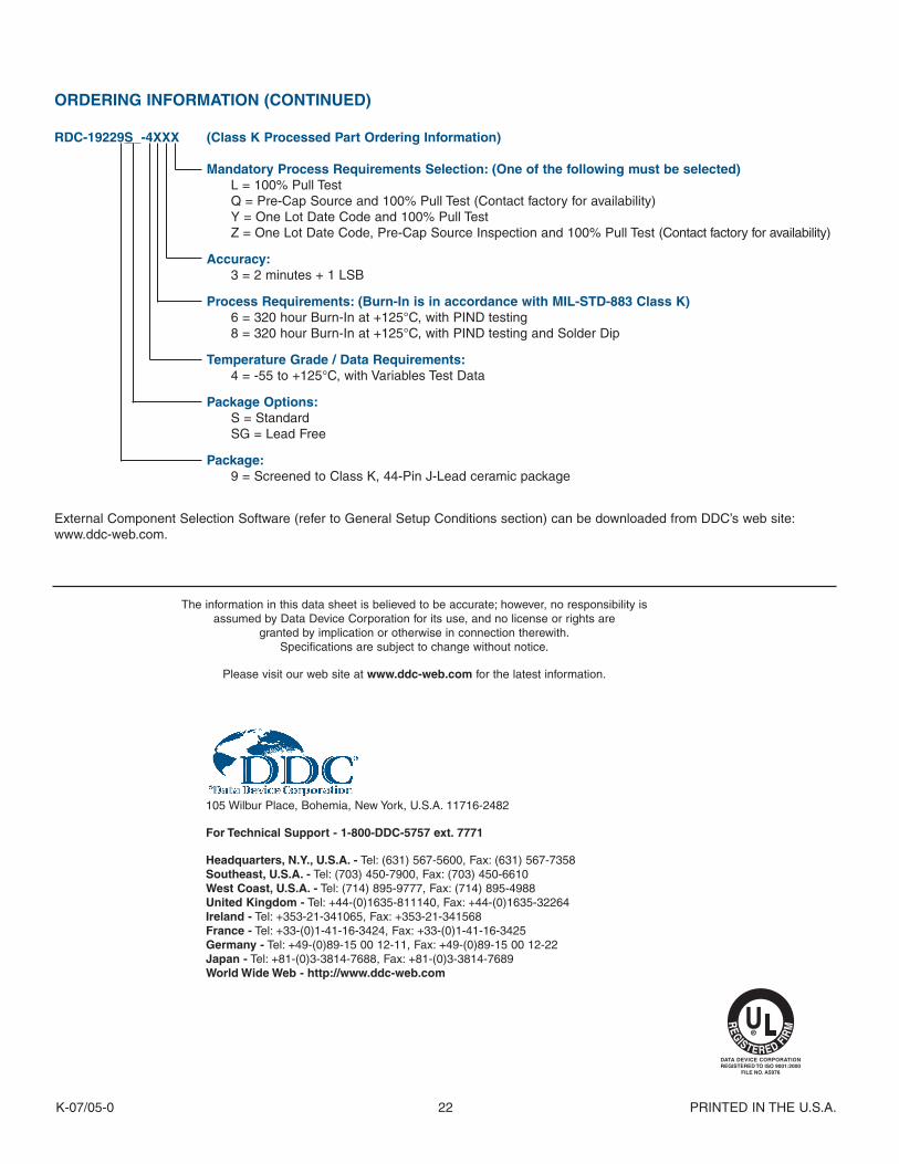
ORDERING INFORMATION (CONTINUED)
RDC-19229S -4XXX (Class K Processed Part Ordering Information)
Mandatory Process Requirements Selection: (One of the following must be selected)L = 100% Pull TestQ = Pre-Cap Source and 100% Pull Test (Contact factory for availability)Y = One Lot Date Code and 100% Pull TestZ = One Lot Date Code, Pre-Cap Source Inspection and 100% Pull Test (Contact factory for availability)
Accuracy:3 = 2 minutes + 1 LSB
Process Requirements: (Burn-In is in accordance with MIL-STD-883 Class K)6 = 320 hour Burn-In at +125°C, with PIND testing8 = 320 hour Burn-In at +125°C, with PIND testing and Solder Dip
Temperature Grade / Data Requirements:4 = -55 to +125°C, with Variables Test Data
Package Options:S = StandardSG = Lead Free
Package:9 = Screened to Class K, 44-Pin J-Lead ceramic package
External Component Selection Software (refer to General Setup Conditions section) can be downloaded from DDC’s web site:www.ddc-web.com.
Related Documents