1120 Int. J. Nanotechnol., Vol. 7, Nos. 9/10/11/12, 2010 Copyright © 2010 Inderscience Enterprises Ltd. Rapid generation of hierarchical nanoarchitectures of CdS via facile microwave assisted hydrothermal/semi-solvothermal route Manish D. Shinde and Amol U. Pawar Centre for Materials for Electronics Technology (C-MET), Plasma and Nanomaterials Laboratory, Panchwati, Pashan Road, Pune 411 008, India E-mail: [email protected] E-mail: [email protected] E-mail: [email protected] V. Sreeja Physical Chemistry Division, National Chemical Laboratory (NCL), Pashan Road, Pune 411 008, India E-mail: [email protected] Sunit Rane Centre for Materials for Electronics Technology (C-MET), Plasma and Nanomaterials Laboratory, Panchwati, Pashan Road, Pune 411 008, India E-mail: [email protected] Hari S. Potdar Physical Chemistry Division, National Chemical Laboratory (NCL), Pashan Road, Pune 411 008, India E-mail: [email protected] Dinesh P. Amalnerkar* Centre for Materials for Electronics Technology (C-MET), Plasma and Nanomaterials Laboratory, Panchwati, Pashan Road, Pune 411 008, India Fax: +91 20 25898180 E-mail: [email protected] E-mail: [email protected] *Corresponding author

Welcome message from author
This document is posted to help you gain knowledge. Please leave a comment to let me know what you think about it! Share it to your friends and learn new things together.
Transcript
1120 Int. J. Nanotechnol., Vol. 7, Nos. 9/10/11/12, 2010
Copyright © 2010 Inderscience Enterprises Ltd.
Rapid generation of hierarchical nanoarchitectures of CdS via facile microwave assisted hydrothermal/semi-solvothermal route
Manish D. Shinde and Amol U. Pawar Centre for Materials for Electronics Technology (C-MET), Plasma and Nanomaterials Laboratory, Panchwati, Pashan Road, Pune 411 008, India E-mail: [email protected] E-mail: [email protected] E-mail: [email protected]
V. Sreeja Physical Chemistry Division, National Chemical Laboratory (NCL), Pashan Road, Pune 411 008, India E-mail: [email protected]
Sunit Rane Centre for Materials for Electronics Technology (C-MET), Plasma and Nanomaterials Laboratory, Panchwati, Pashan Road, Pune 411 008, India E-mail: [email protected]
Hari S. Potdar Physical Chemistry Division, National Chemical Laboratory (NCL), Pashan Road, Pune 411 008, India E-mail: [email protected]
Dinesh P. Amalnerkar* Centre for Materials for Electronics Technology (C-MET), Plasma and Nanomaterials Laboratory, Panchwati, Pashan Road, Pune 411 008, India Fax: +91 20 25898180 E-mail: [email protected] E-mail: [email protected] *Corresponding author
Rapid generation of hierarchical nanoarchitectures 1121
Abstract: 1-D nanorod bundles as well as sea urchin and starfish like hierarchical morphological nanoarchitectures of CdS have been synthesised using a facile microwave assisted hydrothermal/semi-solvothermal technique. Observation of interesting regular/irregular pine-tree like secondary growth over these hierarchical nanoarchitectures is an important aspect of this work. Cadmium acetate and thiourea were used as precursor materials and were dissolved in solution containing mixture of diethylene triamine (DETA) and deionised water (DIW) in different volume ratios prior to subjecting the resultant solution to microwave radiation of 300 W at a reaction time of 10 min and temperature of 140°C. XRD revealed formation of hexagonal CdS with strong (002) preferred orientation (c-axis orientation). Morphology dependent optical properties are studied using room temperature photoluminescence spectroscopy. We feel such secondary growth will be highly favourable in determining the non-linear properties of optoelectronic devices fabricated using such novel hierarchical nanoarchitectures.
Keywords: microwave; solvothermal synthesis; nanorods; hierarchical nanoarchitectures; CdS; secondary growth.
Reference to this paper should be made as follows: Shinde, M.D., Pawar, A.U., Sreeja, V., Rane, S., Potdar, H.S. and Amalnerkar, D.P. (2010) ‘Rapid generation of hierarchical nanoarchitectures of CdS via facile microwave assisted hydrothermal/semi-solvothermal route’, Int. J. Nanotechnol., Vol. 7, Nos. 9/10/11/12, pp.1120–1130.
Biographical notes: Manish D. Shinde obtained his MSc in Physics from University of Pune, India in 2004 and he joined Centre for Materials for Electronics Technology (C-MET), Pune, India in 2004 is now pursuing his PhD from C-MET in Physics. His fields of interest include plasma and green Chemistry Synthesis of nanomaterials and their applications. He has won two awards for oral presentations in various national/international conferences.
Amol U. Pawar obtained his MSc in Physics from the University of Pune, India in 2006. He joined Centre for Materials for Electronics Technology (C-MET), Pune, India in 2006. He is at present pursuing his PhD from Sogang University, Republic of South Korea. He has special interests in plasma technology and photonic nanomaterials.
V. Sreeja is Senior Research Fellow at National Chemical Laboratory, Pune. Her research interest is focused on the synthesis and characterisation of metal oxide nanoparticles for biomedical and engineering applications and developing new and facile synthesis route for the formation of monodispersed nanoparticles as well as various morphologies. Moreover, she likes the surface functionalisation of metal oxide nanoparticles and study the underlying properties of the materials for application point of view.
Sunit Rane joined Centre for Materials for Electronics Technology (C-MET), Pune, India in 1998 as a Scientist. He completed his PhD in ‘Micro-electronics’ in 2000 from Shivaji University, Kolhapur, India. He worked as Post-doctoral fellow at the University of Modena, Italy during 2003–2004. His current research interests include materials science including nanomaterials, LTCC and thick film technology with special interests in microwave packaging components and eco-friendly thick film materials. He has published over 40 papers in various national/international journals.
1122 M.D. Shinde et al.
H.S. Potdar is a Senior Scientist at National Chemical Laboratory, Pune. He joined NCL in 1975 and completed his PhD in 1985 on the topic “Solar selective black coatings for photothermal conversion of solar energy”. His scientific interest focuses on the synthesis of metal oxide nanomaterials with controllable size and morphology from the precursor using wet chemical methods. In addition, focus is to develop processing- structure- property co-relationship in order to get metal oxide powders with reproducible physical and chemical characteristics that are suitable for various applications such as catalysis, sensors and as an anode material in reforming reactions. He has published over 70 papers in various national/international journals. He visited Republic of South Korea as Brain Pool and Kistep fellow during 2002–2003 and 2006–2007.
Dinesh P. Amalnerkar started his research career as Junior Research Fellow at National Chemical Laboratory, Pune and received PhD in Physical Chemistry from University of Pune in 1982. He subsequently worked with Elpro International Ltd. (affiliated to GE, USA) as Scientist till 1985. From January 1986 to April 1987, he had taken up the visiting assignment at Gifu, University, Japan and returned to join the post of Pool Scientist at NCL. He revisited Gifu University, Japan, during September–December 1993 and August–November 2000 as an AIEJ Researcher. In 1991, he joined Centre for Materials for Electronics Technology(C-MET) as a Scientist. Currently, he is the Director of C-MET, Pune. He has published around 95 papers in peer-reviewed international journals, won nine awards for oral/poster presentations in various national/international symposia. There are 13 Indian patents and two technology transfers to his credit. He has contributed a chapter in a book entitled “Thick Film Sensors” published by Elsevier. He is recipient of prestigious Medal Award (for the year 2008) of Materials Research Society of India. He is a member of prominent professional bodies/societies. He is a Fellow of Maharashtra Academy of Sciences, India. Recently (2006–2007), he has worked as a Brain-Pool Visiting Scientist at Korea Research Institute of Chemical Technology, Daejon, Korea.
1 Introduction
Control over shape and size of inorganic nanostructures (which, in turn, determine their optical as well as electronic properties) is very important in terms of realising their applications in nanoelectronics and optoelectronics. Synthesis of hierarchical nanoscale structures with control over the size and shape is even more challenging in terms of the complexities of the process parameters involved. Cadmium sulphide (CdS) with a direct band gap of 2.4 eV at room temperature is a natural material choice for various optoelectronic devices such as non-linear optical devices, flat panel displays, light emitting diodes, and lasers. As a consequence, various methods have been explored for synthesis of hierarchical nanoscale morphologies of CdS. There are few synthesis techniques developed so far to prepare various hierarchical nanoarchitectures of CdS like directed assembly of hierarchical CdS nanotube arrays from CdS nanoparticles using anodic aluminium oxide (AAO) template [1], synthesis of large-scale hierarchical dendrites of single-crystal CdS by hydrothermal treatment [2], sonochemistry-assisted microwave synthesis of single-crystalline CdS nanoflowers [3], catalyst-assisted vapour-liquid-solid (VLS) growth technique for synthesis of branched CdS
Rapid generation of hierarchical nanoarchitectures 1123
nanostructures [4], and fabrication of rocket like tetrapodal nanorods by seed-epitaxial metal-organic chemical vapour deposition [5] etc. Recently, Yao et al proposed a facile solvothermal approach (with conventional heating) to produce CdS nanostructures with complex morphologies such as nanoflowers, fractal nanotrees etc for furnishing greater functionality [6]. The method proposed by Yao et al. was further modified by Amalnerkar et al. [7] to adapt to microwave solvothermal reaction technique in order to drastically reduce the reaction time (to 1 h as compared to 12 h by Yao et al.). They carried out the reaction at 180°C, which was a pre-selected value in accordance with earlier work of Yao et al. Keeping in view of the immense reaction kinetics that microwave source can provide and also to follow the ‘greener path’ (i.e., less energy intensive) of the reaction, we decided to further explore the feasibility of carrying out the reaction in a single step with microwave power source of 300 W and at reduced temperature of 140ºC and reaction time of 10 min. We investigated the effect of variation of these reaction parameters on morphological properties of the resultant CdS architectures. We followed the same procedure adopted by Amalnerkar et al. Moreover, in order to compare our results on synthesis of hierarchical nano architectures using semi-solvothermal route to that with hydrothermal route (specifically with respect to morphological as well optical properties), we carried out the same reaction without using DETA i.e., for DETA/DIW volume ratio of 0 : 6 (i.e., microwave-assisted hydrothermal route). We found that the resultant nanoscale architectural features are dependent on the type of solvents, their volume ratios in a given mixture as well as on the applied power. The preliminary physico-chemical examination of the resultant products by XRD and SEM as well as TEM revealed nanoscale formation of sea urchin and starfish like morphological features of hexagonal CdS with strong (002) preferred orientation (c-axis orientation). Regular as well as irregular secondary growth over the nanoscale 1-D structures shows the appearance of pine-tree like architectures. We feel that such secondary growth will be highly favourable in determining the non-linear properties of optoelectronic devices fabricated by using such novel hierarchical nanoarchitectures. The room temperature photoluminescence (PL) spectra give information about morphology dependent optical properties of the prepared nanostructures. We herein, report the details of the findings associated with the synthesis of hierarchical nanoarchitectures of CdS at reduced temperature, time having the secondary growth over 1-D nanostructures.
2 Experimental details
2.1 Microwave-assisted semisolvothermal synthesis
Even though we have followed the similar procedure as reported by Amalnerkar et al., we carried out the reaction at a reduced processing temperature. In addition, we carried out the reaction using microwave assisted hyrdrothermal technique for the sake of comparison of obtained data. In a typical procedure, 0.1596 g of cadmium acetate dihydrate (0.6 mmol) and 0.0456 g of thiourea (0.6 mmol) were added into a mixed solution of diethylenetriamine (DETA) and deionised water (DIW) with volume ratios of 1 : 6, 1 : 1, 6 : 1 and 0 : 6. The resultant mixture (total volume 30 ml) was loaded in a 100 ml teflon autoclave, which was sealed and placed in a microwave oven (MARS 5, CEM Corp., maximum operating power 1200 W). The system was quickly raised to the
1124 M.D. Shinde et al.
temperature of 140°C in 3 min with microwave power of 300 W and maintained at this temperature for 7 min with microwave power of 300 W (i.e., total reaction time of 10 min). Subsequently, the autoclave was naturally cooled down to room temperature. After the reaction, the solution was centrifuged and the collected solid mass was successively washed with deionised water and absolute alcohol, recovered with centrifugation and dried in vacuum at 80°C for 8 h. The colour of the resultant dried powders varied from bright yellow to orange yellow depending upon reaction conditions. Approximate yield of CdS was about 20%. This observation leads to conclusion that use of microwave power of 300 W in a single step does not have any effect on the yield of the resultant product. Interestingly, the yield was even higher (about 40%) for samples prepared via microwave assisted hydrothermal route (i.e., DETA: DIW ratio of 0 : 6).
2.2 Characterisation
Crystal structure determination was carried out by recording X-ray diffractograms on Rigaku miniflex diffractometer using Ni filtered Cu Kα radiation. Micro-scale and nano-scale morphological aspects of the samples were examined by scanning electron microscopy (Philips, XL 30S FEG). Fine-scale microstructure examination was performed by transmission electron microscopy (FEI Quanta 200 ESEM). Photoluminescence spectra were obtained with Shimadzu RF 5301 PC photoluminescence spectrometer using xenon flash lamp at an excitation wavelength of 400 nm.
3 Results and discussion
3.1 X-ray diffraction analysis
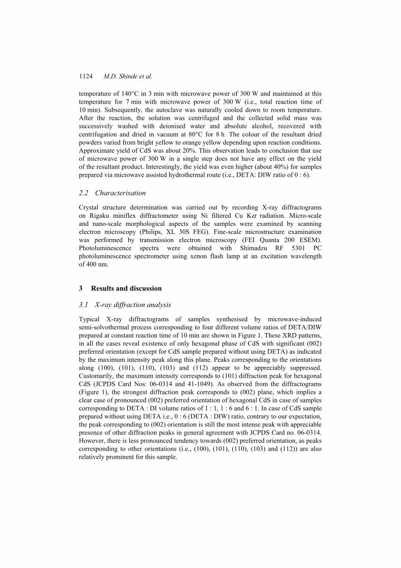
Typical X-ray diffractograms of samples synthesised by microwave-induced semi-solvothermal process corresponding to four different volume ratios of DETA/DIW prepared at constant reaction time of 10 min are shown in Figure 1. These XRD patterns, in all the cases reveal existence of only hexagonal phase of CdS with significant (002) preferred orientation (except for CdS sample prepared without using DETA) as indicated by the maximum intensity peak along this plane. Peaks corresponding to the orientations along (100), (101), (110), (103) and (112) appear to be appreciably suppressed. Customarily, the maximum intensity corresponds to (101) diffraction peak for hexagonal CdS (JCPDS Card Nos: 06-0314 and 41-1049). As observed from the diffractograms (Figure 1), the strongest diffraction peak corresponds to (002) plane, which implies a clear case of pronounced (002) preferred orientation of hexagonal CdS in case of samples corresponding to DETA : DI volume ratios of 1 : 1, 1 : 6 and 6 : 1. In case of CdS sample prepared without using DETA i.e., 0 : 6 (DETA : DIW) ratio, contrary to our expectation, the peak corresponding to (002) orientation is still the most intense peak with appreciable presence of other diffraction peaks in general agreement with JCPDS Card no. 06-0314. However, there is less pronounced tendency towards (002) preferred orientation, as peaks corresponding to other orientations (i.e., (100), (101), (110), (103) and (112)) are also relatively prominent for this sample.
Rapid generation of hierarchical nanoarchitectures 1125
Figure 1 Typical X-ray diffractograms of CdS powders corresponding to DETA: DIW volume ratio of (a) 0 : 6; (b) 1 : 1; (c) 1 : 6 and (d) 6 : 1 (see online version for colours)
The peak broadening observed in almost all X-ray diffractograms is the preliminary but definite indication of formation of nanosized products in our case. The peak broadening is more pronounced for samples corresponding to 1 : 1, 1 : 6, 6 : 1 DETA: DIW ratios but is feebly observed for sample corresponding to 0 : 6 DETA/DIW volume ratio. The primary particle size (crystallite size) has been calculated from FWHM values of diffraction peaks corresponding to (002) plane using the Scherrer equation. Such an exercise furnished the particle size values in the range of 11–24 nm for (002) diffraction peak depending upon solvent-volume ratio and reaction time conditions.
3.2 SEM analysis
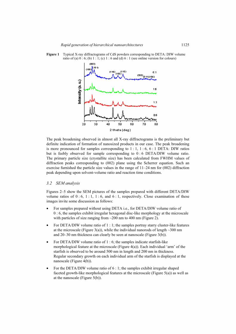
Figures 2–5 show the SEM pictures of the samples prepared with different DETA/DIW volume ratios of 0 : 6, 1 : 1, 1 : 6, and 6 : 1, respectively. Close examination of these images invite some discussion as follows:
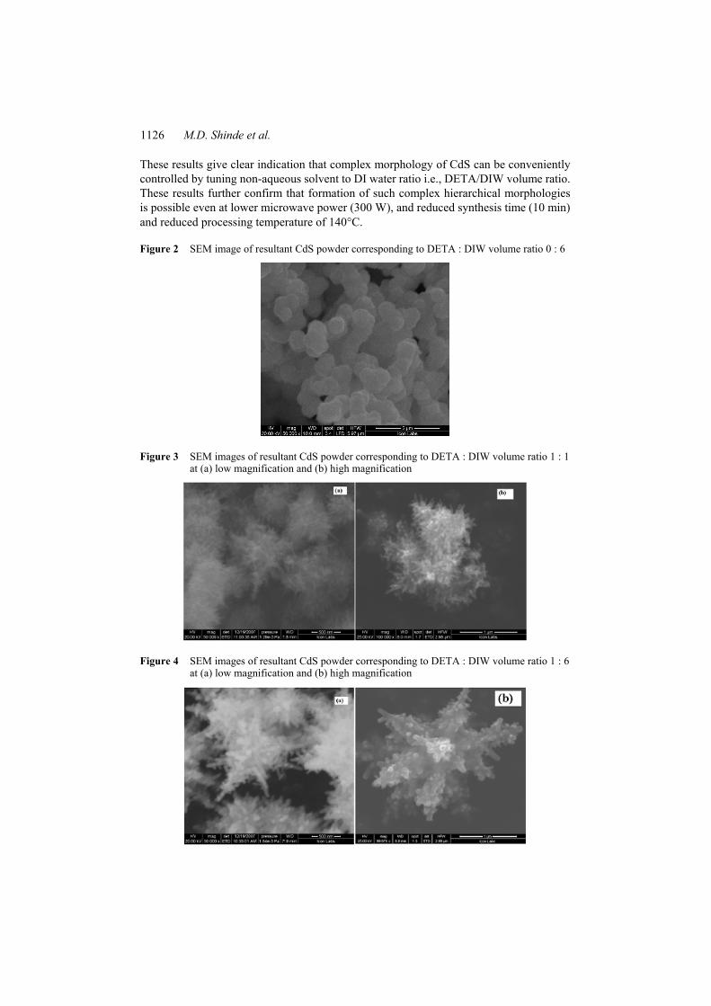
• For samples prepared without using DETA i.e., for DETA/DIW volume ratio of 0 : 6, the samples exhibit irregular hexagonal disc-like morphology at the microscale with particles of size ranging from ~200 nm to 400 nm (Figure 2).
• For DETA/DIW volume ratio of 1 : 1; the samples portray starry cluster-like features at the microscale (Figure 3(a)), while the individual nanorods of length ~300 nm and 20–30 nm thickness can clearly be seen at nanoscale (Figure 3(b)).
• For DETA/DIW volume ratio of 1 : 6; the samples indicate starfish-like morphological feature at the microscale (Figure 4(a)). Each individual ‘arm’ of the starfish is observed to be around 500 nm in length and 200 nm in thickness. Regular secondary growth on each individual arm of the starfish is displayed at the nanoscale (Figure 4(b)).
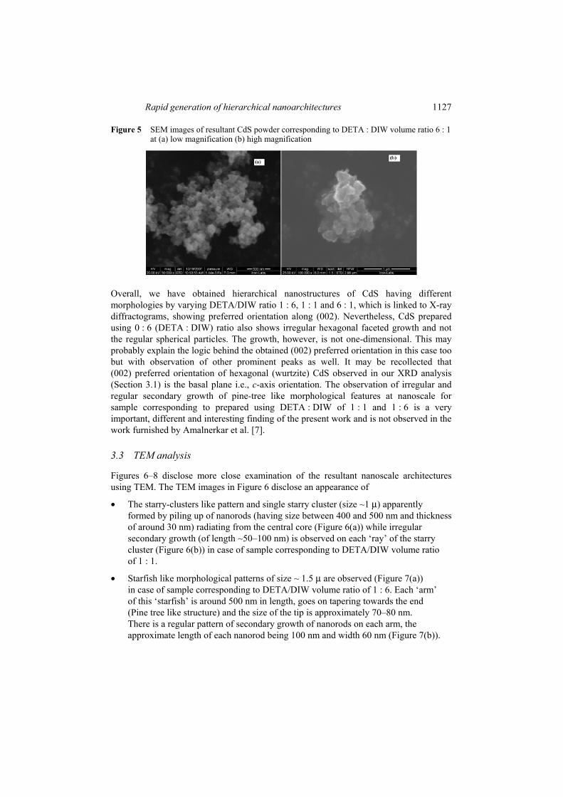
• For the DETA/DIW volume ratio of 6 : 1; the samples exhibit irregular shaped faceted growth-like morphological features at the microscale (Figure 5(a)) as well as at the nanoscale (Figure 5(b)).
1126 M.D. Shinde et al.
These results give clear indication that complex morphology of CdS can be conveniently controlled by tuning non-aqueous solvent to DI water ratio i.e., DETA/DIW volume ratio. These results further confirm that formation of such complex hierarchical morphologies is possible even at lower microwave power (300 W), and reduced synthesis time (10 min) and reduced processing temperature of 140°C.
Figure 2 SEM image of resultant CdS powder corresponding to DETA : DIW volume ratio 0 : 6
Figure 3 SEM images of resultant CdS powder corresponding to DETA : DIW volume ratio 1 : 1 at (a) low magnification and (b) high magnification
Figure 4 SEM images of resultant CdS powder corresponding to DETA : DIW volume ratio 1 : 6 at (a) low magnification and (b) high magnification
Rapid generation of hierarchical nanoarchitectures 1127
Figure 5 SEM images of resultant CdS powder corresponding to DETA : DIW volume ratio 6 : 1 at (a) low magnification (b) high magnification
Overall, we have obtained hierarchical nanostructures of CdS having different morphologies by varying DETA/DIW ratio 1 : 6, 1 : 1 and 6 : 1, which is linked to X-ray diffractograms, showing preferred orientation along (002). Nevertheless, CdS prepared using 0 : 6 (DETA : DIW) ratio also shows irregular hexagonal faceted growth and not the regular spherical particles. The growth, however, is not one-dimensional. This may probably explain the logic behind the obtained (002) preferred orientation in this case too but with observation of other prominent peaks as well. It may be recollected that (002) preferred orientation of hexagonal (wurtzite) CdS observed in our XRD analysis (Section 3.1) is the basal plane i.e., c-axis orientation. The observation of irregular and regular secondary growth of pine-tree like morphological features at nanoscale for sample corresponding to prepared using DETA : DIW of 1 : 1 and 1 : 6 is a very important, different and interesting finding of the present work and is not observed in the work furnished by Amalnerkar et al. [7].
3.3 TEM analysis
Figures 6–8 disclose more close examination of the resultant nanoscale architectures using TEM. The TEM images in Figure 6 disclose an appearance of
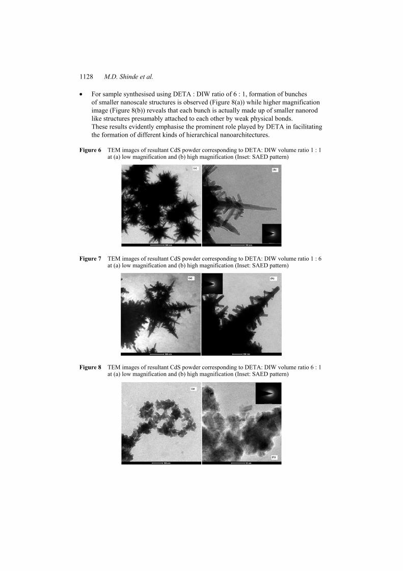
• The starry-clusters like pattern and single starry cluster (size ~1 µ) apparently formed by piling up of nanorods (having size between 400 and 500 nm and thickness of around 30 nm) radiating from the central core (Figure 6(a)) while irregular secondary growth (of length ~50–100 nm) is observed on each ‘ray’ of the starry cluster (Figure 6(b)) in case of sample corresponding to DETA/DIW volume ratio of 1 : 1.
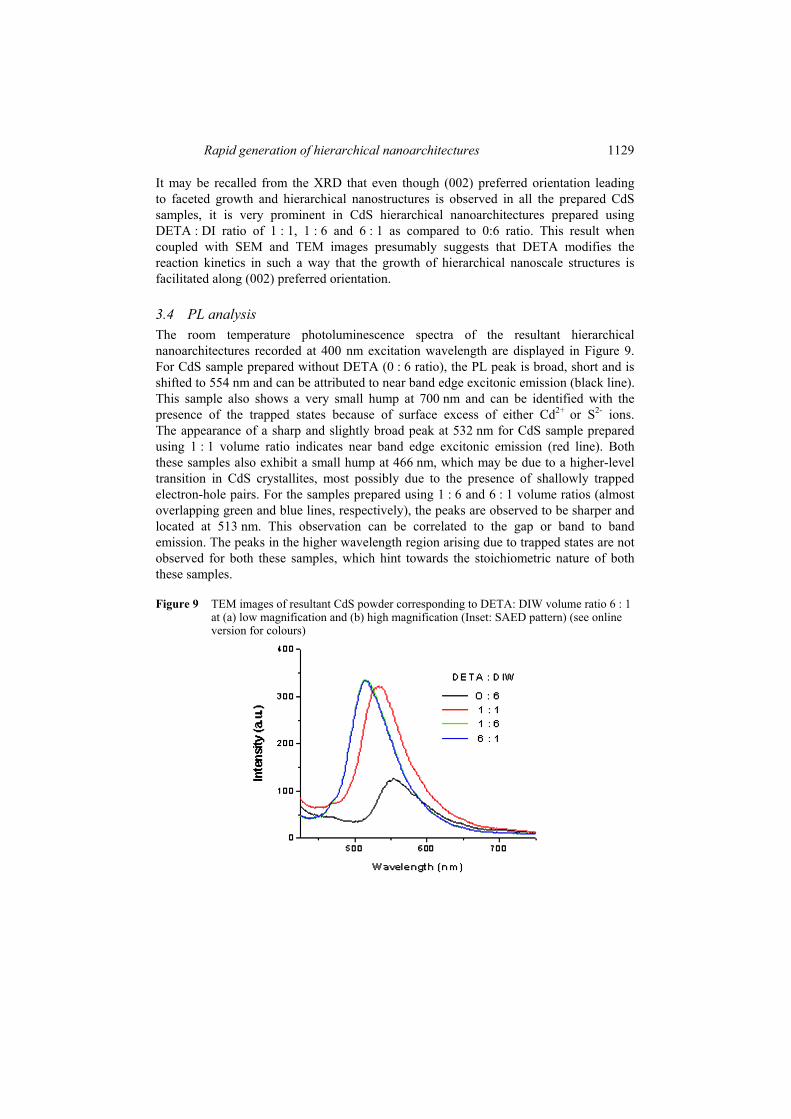
• Starfish like morphological patterns of size ~ 1.5 µ are observed (Figure 7(a)) in case of sample corresponding to DETA/DIW volume ratio of 1 : 6. Each ‘arm’ of this ‘starfish’ is around 500 nm in length, goes on tapering towards the end (Pine tree like structure) and the size of the tip is approximately 70–80 nm. There is a regular pattern of secondary growth of nanorods on each arm, the approximate length of each nanorod being 100 nm and width 60 nm (Figure 7(b)).
1128 M.D. Shinde et al.
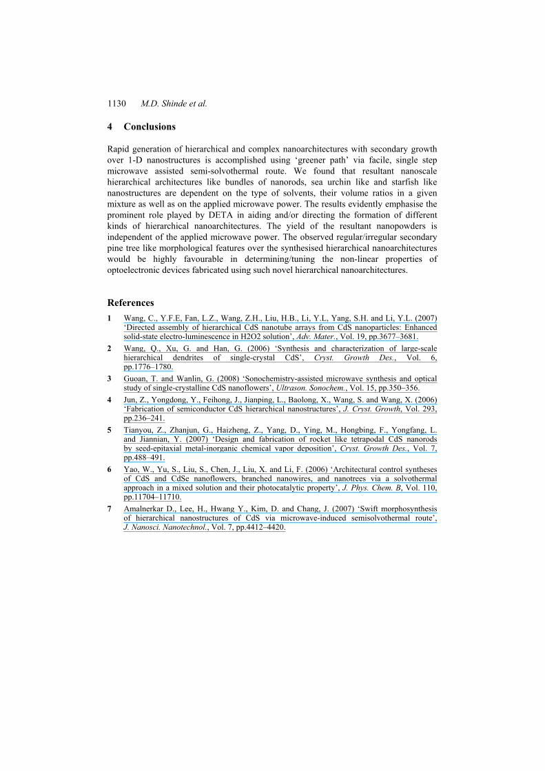
• For sample synthesised using DETA : DIW ratio of 6 : 1, formation of bunches of smaller nanoscale structures is observed (Figure 8(a)) while higher magnification image (Figure 8(b)) reveals that each bunch is actually made up of smaller nanorod like structures presumably attached to each other by weak physical bonds. These results evidently emphasise the prominent role played by DETA in facilitating the formation of different kinds of hierarchical nanoarchitectures.
Figure 6 TEM images of resultant CdS powder corresponding to DETA: DIW volume ratio 1 : 1 at (a) low magnification and (b) high magnification (Inset: SAED pattern)
Figure 7 TEM images of resultant CdS powder corresponding to DETA: DIW volume ratio 1 : 6 at (a) low magnification and (b) high magnification (Inset: SAED pattern)
Figure 8 TEM images of resultant CdS powder corresponding to DETA: DIW volume ratio 6 : 1 at (a) low magnification and (b) high magnification (Inset: SAED pattern)
Rapid generation of hierarchical nanoarchitectures 1129
It may be recalled from the XRD that even though (002) preferred orientation leading to faceted growth and hierarchical nanostructures is observed in all the prepared CdS samples, it is very prominent in CdS hierarchical nanoarchitectures prepared using DETA : DI ratio of 1 : 1, 1 : 6 and 6 : 1 as compared to 0:6 ratio. This result when coupled with SEM and TEM images presumably suggests that DETA modifies the reaction kinetics in such a way that the growth of hierarchical nanoscale structures is facilitated along (002) preferred orientation.
3.4 PL analysis The room temperature photoluminescence spectra of the resultant hierarchical nanoarchitectures recorded at 400 nm excitation wavelength are displayed in Figure 9. For CdS sample prepared without DETA (0 : 6 ratio), the PL peak is broad, short and is shifted to 554 nm and can be attributed to near band edge excitonic emission (black line). This sample also shows a very small hump at 700 nm and can be identified with the presence of the trapped states because of surface excess of either Cd2+ or S2- ions. The appearance of a sharp and slightly broad peak at 532 nm for CdS sample prepared using 1 : 1 volume ratio indicates near band edge excitonic emission (red line). Both these samples also exhibit a small hump at 466 nm, which may be due to a higher-level transition in CdS crystallites, most possibly due to the presence of shallowly trapped electron-hole pairs. For the samples prepared using 1 : 6 and 6 : 1 volume ratios (almost overlapping green and blue lines, respectively), the peaks are observed to be sharper and located at 513 nm. This observation can be correlated to the gap or band to band emission. The peaks in the higher wavelength region arising due to trapped states are not observed for both these samples, which hint towards the stoichiometric nature of both these samples.
Figure 9 TEM images of resultant CdS powder corresponding to DETA: DIW volume ratio 6 : 1 at (a) low magnification and (b) high magnification (Inset: SAED pattern) (see online version for colours)
1130 M.D. Shinde et al.
4 Conclusions
Rapid generation of hierarchical and complex nanoarchitectures with secondary growth over 1-D nanostructures is accomplished using ‘greener path’ via facile, single step microwave assisted semi-solvothermal route. We found that resultant nanoscale hierarchical architectures like bundles of nanorods, sea urchin like and starfish like nanostructures are dependent on the type of solvents, their volume ratios in a given mixture as well as on the applied microwave power. The results evidently emphasise the prominent role played by DETA in aiding and/or directing the formation of different kinds of hierarchical nanoarchitectures. The yield of the resultant nanopowders is independent of the applied microwave power. The observed regular/irregular secondary pine tree like morphological features over the synthesised hierarchical nanoarchitectures would be highly favourable in determining/tuning the non-linear properties of optoelectronic devices fabricated using such novel hierarchical nanoarchitectures.
References 1 Wang, C., Y.F.E, Fan, L.Z., Wang, Z.H., Liu, H.B., Li, Y.L, Yang, S.H. and Li, Y.L. (2007)
‘Directed assembly of hierarchical CdS nanotube arrays from CdS nanoparticles: Enhanced solid-state electro-luminescence in H2O2 solution’, Adv. Mater., Vol. 19, pp.3677–3681.
2 Wang, Q., Xu, G. and Han, G. (2006) ‘Synthesis and characterization of large-scale hierarchical dendrites of single-crystal CdS’, Cryst. Growth Des., Vol. 6, pp.1776–1780.
3 Guoan, T. and Wanlin, G. (2008) ‘Sonochemistry-assisted microwave synthesis and optical study of single-crystalline CdS nanoflowers’, Ultrason. Sonochem., Vol. 15, pp.350–356.
4 Jun, Z., Yongdong, Y., Feihong, J., Jianping, L., Baolong, X., Wang, S. and Wang, X. (2006) ‘Fabrication of semiconductor CdS hierarchical nanostructures’, J. Cryst. Growth, Vol. 293, pp.236–241.
5 Tianyou, Z., Zhanjun, G., Haizheng, Z., Yang, D., Ying, M., Hongbing, F., Yongfang, L. and Jiannian, Y. (2007) ‘Design and fabrication of rocket like tetrapodal CdS nanorods by seed-epitaxial metal-inorganic chemical vapor deposition’, Cryst. Growth Des., Vol. 7, pp.488–491.
6 Yao, W., Yu, S., Liu, S., Chen, J., Liu, X. and Li, F. (2006) ‘Architectural control syntheses of CdS and CdSe nanoflowers, branched nanowires, and nanotrees via a solvothermal approach in a mixed solution and their photocatalytic property’, J. Phys. Chem. B, Vol. 110, pp.11704–11710.
7 Amalnerkar D., Lee, H., Hwang Y., Kim, D. and Chang, J. (2007) ‘Swift morphosynthesis of hierarchical nanostructures of CdS via microwave-induced semisolvothermal route’, J. Nanosci. Nanotechnol., Vol. 7, pp.4412–4420.
Related Documents


