Random Number Generator Dmitriy Solmonov W1-1 David Levitt W1-2 Jesse Guss W1-3 Sirisha Pillalamarri W1-4 Matt Russo W1-5 Design Manager – Thiago Hersan February 22, 2006 Top Level Integration ct Objective: e a Cryptologically Secure Pseudo-Random Number Generator

Random Number Generator Dmitriy Solmonov W1-1 David Levitt W1-2 Jesse Guss W1-3 Sirisha Pillalamarri W1-4 Matt Russo W1-5 Design Manager – Thiago Hersan.
Dec 14, 2015
Welcome message from author
This document is posted to help you gain knowledge. Please leave a comment to let me know what you think about it! Share it to your friends and learn new things together.
Transcript
Random Number Generator
Dmitriy Solmonov W1-1David Levitt W1-2Jesse Guss W1-3
Sirisha Pillalamarri W1-4 Matt Russo W1-5
Design Manager – Thiago Hersan
February 22, 2006Top Level Integration
Project Objective:Create a Cryptologically Secure Pseudo-Random Number Generator

Agenda• Status
• Design Decisions
• Timing Constraints
• Timing Analysis
• Power Analysis
• Registers

StatusCompleted C implementation Architecture Behavioral Design and Simulation Gate-Level Design and Simulation Preliminary FloorplanIn Progress Schematic Design and Simulation (90% Done) LayoutUnfinished• Extraction, LVS, post-layout simulation
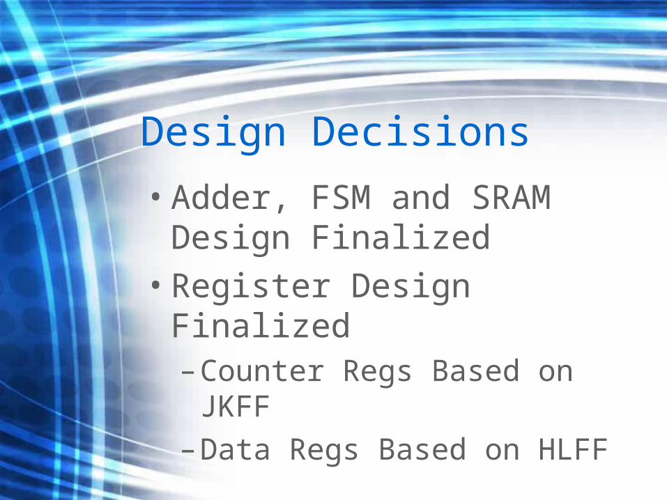
Design Decisions
• Adder, FSM and SRAM Design Finalized
• Register Design Finalized– Counter Regs Based on JKFF
– Data Regs Based on HLFF
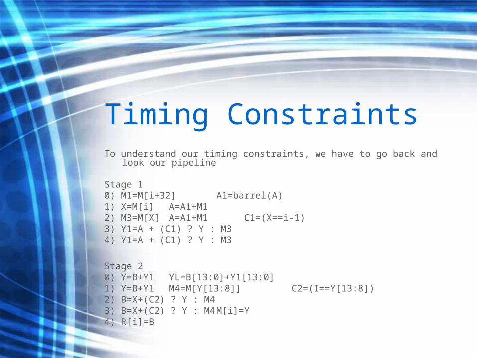
Timing ConstraintsTo understand our timing constraints, we have to go back and look our pipeline
Stage 10) M1=M[i+32] A1=barrel(A) 1) X=M[i] A=A1+M1 2) M3=M[X] A=A1+M1 C1=(X==i-1) 3) Y1=A + (C1) ? Y : M3 4) Y1=A + (C1) ? Y : M3
Stage 2 0) Y=B+Y1 YL=B[13:0]+Y1[13:0] 1) Y=B+Y1 M4=M[Y[13:8]] C2=(I==Y[13:8]) 2) B=X+(C2) ? Y : M4 3) B=X+(C2) ? Y : M4 M[i]=Y 4) R[i]=B
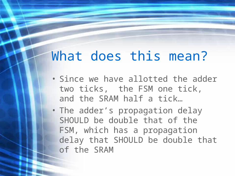
What does this mean?
• Since we have allotted the adder two ticks, the FSM one tick, and the SRAM half a tick…
• The adder’s propagation delay SHOULD be double that of the FSM, which has a propagation delay that SHOULD be double that of the SRAM

Timing Analysis - Adder
• Since our adder is so complicated we were unsure how to locate the critical path on the schematic by hand
• We found the critical path of the adder to be from the B[4] pin to the S[31] pin using Pathmill

Timing Analysis - Adder
Total Prop Delay:1.44ns
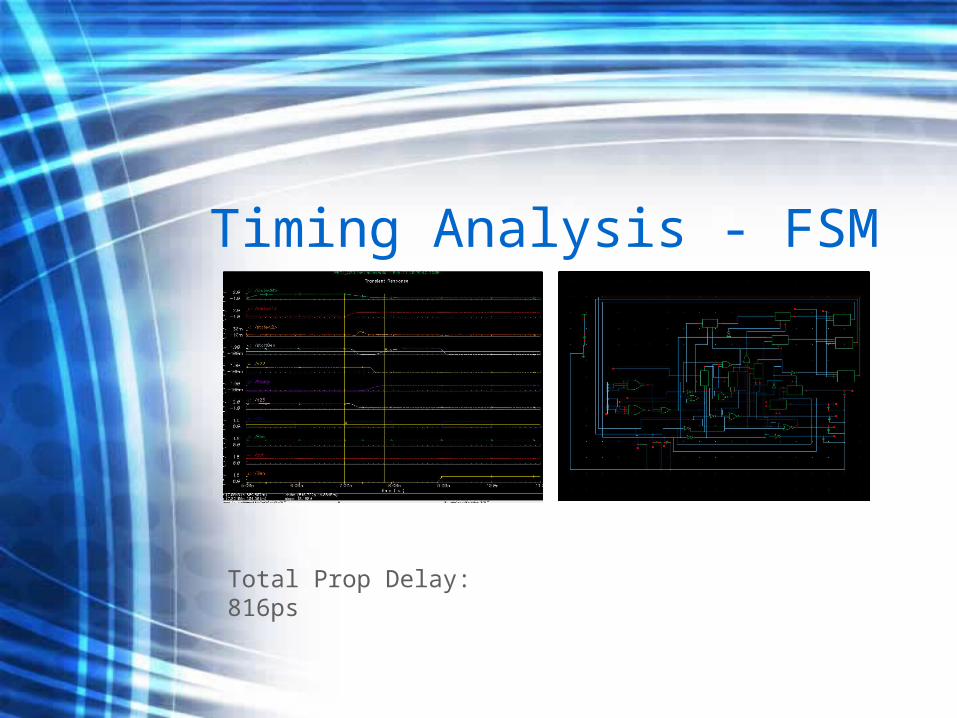
Timing Analysis - FSM
Total Prop Delay:816ps
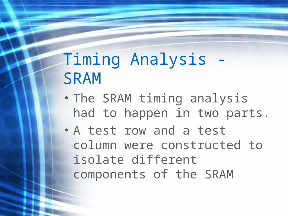
Timing Analysis - SRAM
• The SRAM timing analysis had to happen in two parts.
• A test row and a test column were constructed to isolate different components of the SRAM
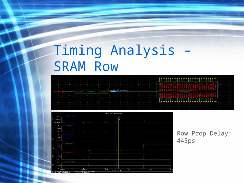
Timing Analysis – SRAM Row
Row Prop Delay:445ps

Timing Analysis – SRAM Column
Column Prop Delay:290psTotal Prop Delay:735ps

Putting it All TogetherComponent Transistor Count Area Prop
Delay
Power
Adders (4x) 5856
(1464 each)
2700um2
(675um2 ea.)
1.44ns 888uW
FSM 194 100um2 826ps 46uW
SRAM 17736
(M=10458 R=7278)
8000um2 735ps W: 510uW
R: 190uW
Datapath
w/o Adders
10924 5000um2
Total 34710 15800um2 TBD TBD

Registers
• Using JKFF for Counter Regs
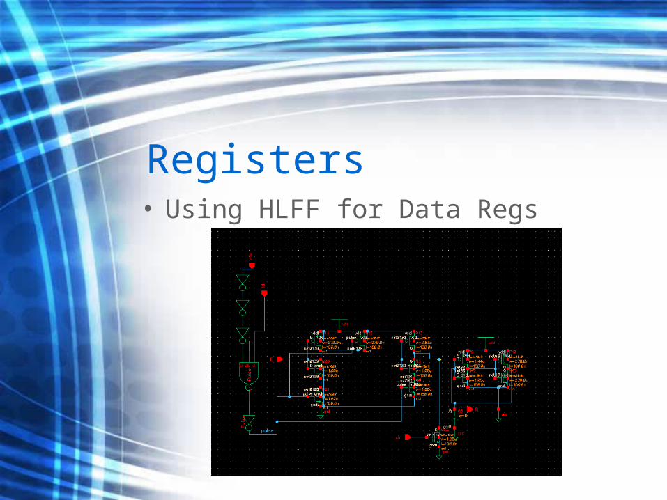
Registers• Using HLFF for Data Regs
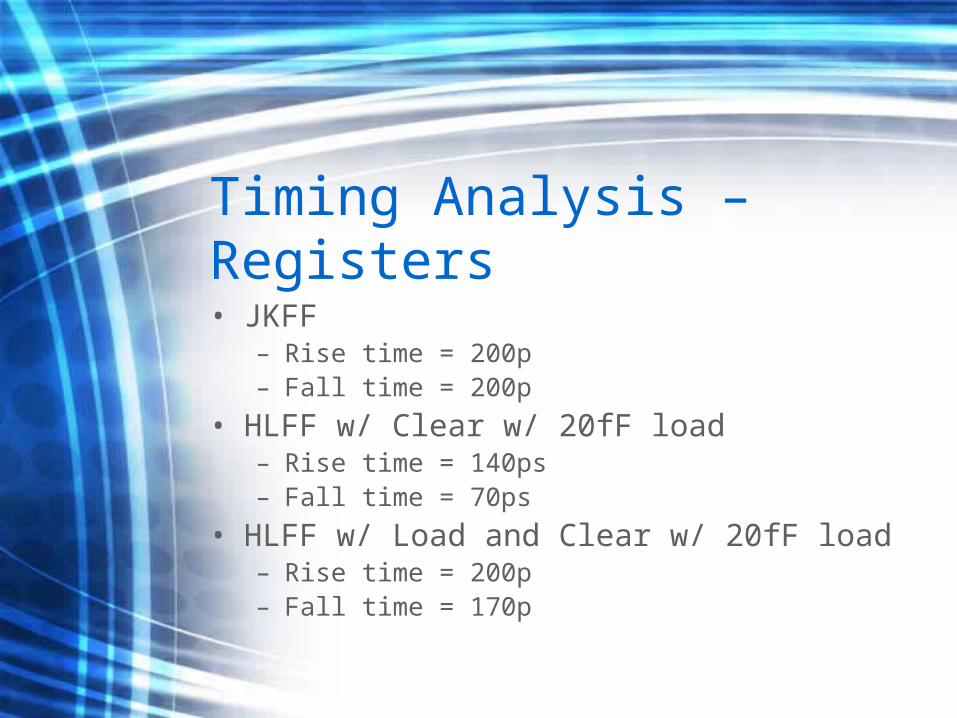
Timing Analysis – Registers• JKFF
– Rise time = 200p– Fall time = 200p
• HLFF w/ Clear w/ 20fF load– Rise time = 140ps– Fall time = 70ps
• HLFF w/ Load and Clear w/ 20fF load– Rise time = 200p – Fall time = 170p

Thanks!
Any Questions?
Related Documents


![ppQ JH]DPHOLMN ELMJHERXZ - commissiemer.nl filewa wa wa wa wa wa wa wa wa wa wa wa wa wa wa wa wa bo bo bo w1 w1 w1 w1 w1 w1 w1 w1 w1 w1 w1 w1 w1 w1 w1 w1 w1 w1 w1 w1 w1 w1 w1 w1 w1](https://static.cupdf.com/doc/110x72/5e1a81165044c7664e160d6d/ppq-jhdpholmn-elmjherxz-wa-wa-wa-wa-wa-wa-wa-wa-wa-wa-wa-wa-wa-wa-wa-wa-bo-bo.jpg)

